JP4244321B2 - Light switching device - Google Patents
Light switching device Download PDFInfo
- Publication number
- JP4244321B2 JP4244321B2 JP2003520203A JP2003520203A JP4244321B2 JP 4244321 B2 JP4244321 B2 JP 4244321B2 JP 2003520203 A JP2003520203 A JP 2003520203A JP 2003520203 A JP2003520203 A JP 2003520203A JP 4244321 B2 JP4244321 B2 JP 4244321B2
- Authority
- JP
- Japan
- Prior art keywords
- light
- polarization
- polarizer
- mode
- birefringent
- Prior art date
- Legal status (The legal status is an assumption and is not a legal conclusion. Google has not performed a legal analysis and makes no representation as to the accuracy of the status listed.)
- Expired - Lifetime
Links
Images


Classifications
-
- G—PHYSICS
- G02—OPTICS
- G02F—OPTICAL DEVICES OR ARRANGEMENTS FOR THE CONTROL OF LIGHT BY MODIFICATION OF THE OPTICAL PROPERTIES OF THE MEDIA OF THE ELEMENTS INVOLVED THEREIN; NON-LINEAR OPTICS; FREQUENCY-CHANGING OF LIGHT; OPTICAL LOGIC ELEMENTS; OPTICAL ANALOGUE/DIGITAL CONVERTERS
- G02F1/00—Devices or arrangements for the control of the intensity, colour, phase, polarisation or direction of light arriving from an independent light source, e.g. switching, gating or modulating; Non-linear optics
- G02F1/01—Devices or arrangements for the control of the intensity, colour, phase, polarisation or direction of light arriving from an independent light source, e.g. switching, gating or modulating; Non-linear optics for the control of the intensity, phase, polarisation or colour
- G02F1/13—Devices or arrangements for the control of the intensity, colour, phase, polarisation or direction of light arriving from an independent light source, e.g. switching, gating or modulating; Non-linear optics for the control of the intensity, phase, polarisation or colour based on liquid crystals, e.g. single liquid crystal display cells
- G02F1/1326—Liquid crystal optical waveguides or liquid crystal cells specially adapted for gating or modulating between optical waveguides
-
- G—PHYSICS
- G02—OPTICS
- G02B—OPTICAL ELEMENTS, SYSTEMS OR APPARATUS
- G02B30/00—Optical systems or apparatus for producing three-dimensional [3D] effects, e.g. stereoscopic images
- G02B30/20—Optical systems or apparatus for producing three-dimensional [3D] effects, e.g. stereoscopic images by providing first and second parallax images to an observer's left and right eyes
- G02B30/22—Optical systems or apparatus for producing three-dimensional [3D] effects, e.g. stereoscopic images by providing first and second parallax images to an observer's left and right eyes of the stereoscopic type
- G02B30/25—Optical systems or apparatus for producing three-dimensional [3D] effects, e.g. stereoscopic images by providing first and second parallax images to an observer's left and right eyes of the stereoscopic type using polarisation techniques
-
- G—PHYSICS
- G02—OPTICS
- G02B—OPTICAL ELEMENTS, SYSTEMS OR APPARATUS
- G02B30/00—Optical systems or apparatus for producing three-dimensional [3D] effects, e.g. stereoscopic images
- G02B30/20—Optical systems or apparatus for producing three-dimensional [3D] effects, e.g. stereoscopic images by providing first and second parallax images to an observer's left and right eyes
- G02B30/26—Optical systems or apparatus for producing three-dimensional [3D] effects, e.g. stereoscopic images by providing first and second parallax images to an observer's left and right eyes of the autostereoscopic type
- G02B30/27—Optical systems or apparatus for producing three-dimensional [3D] effects, e.g. stereoscopic images by providing first and second parallax images to an observer's left and right eyes of the autostereoscopic type involving lenticular arrays
-
- G—PHYSICS
- G02—OPTICS
- G02F—OPTICAL DEVICES OR ARRANGEMENTS FOR THE CONTROL OF LIGHT BY MODIFICATION OF THE OPTICAL PROPERTIES OF THE MEDIA OF THE ELEMENTS INVOLVED THEREIN; NON-LINEAR OPTICS; FREQUENCY-CHANGING OF LIGHT; OPTICAL LOGIC ELEMENTS; OPTICAL ANALOGUE/DIGITAL CONVERTERS
- G02F1/00—Devices or arrangements for the control of the intensity, colour, phase, polarisation or direction of light arriving from an independent light source, e.g. switching, gating or modulating; Non-linear optics
- G02F1/01—Devices or arrangements for the control of the intensity, colour, phase, polarisation or direction of light arriving from an independent light source, e.g. switching, gating or modulating; Non-linear optics for the control of the intensity, phase, polarisation or colour
- G02F1/13—Devices or arrangements for the control of the intensity, colour, phase, polarisation or direction of light arriving from an independent light source, e.g. switching, gating or modulating; Non-linear optics for the control of the intensity, phase, polarisation or colour based on liquid crystals, e.g. single liquid crystal display cells
- G02F1/133—Constructional arrangements; Operation of liquid crystal cells; Circuit arrangements
- G02F1/1333—Constructional arrangements; Manufacturing methods
- G02F1/1335—Structural association of cells with optical devices, e.g. polarisers or reflectors
- G02F1/133526—Lenses, e.g. microlenses or Fresnel lenses
-
- H—ELECTRICITY
- H04—ELECTRIC COMMUNICATION TECHNIQUE
- H04N—PICTORIAL COMMUNICATION, e.g. TELEVISION
- H04N13/00—Stereoscopic video systems; Multi-view video systems; Details thereof
- H04N13/30—Image reproducers
- H04N13/302—Image reproducers for viewing without the aid of special glasses, i.e. using autostereoscopic displays
- H04N13/305—Image reproducers for viewing without the aid of special glasses, i.e. using autostereoscopic displays using lenticular lenses, e.g. arrangements of cylindrical lenses
-
- H—ELECTRICITY
- H04—ELECTRIC COMMUNICATION TECHNIQUE
- H04N—PICTORIAL COMMUNICATION, e.g. TELEVISION
- H04N13/00—Stereoscopic video systems; Multi-view video systems; Details thereof
- H04N13/30—Image reproducers
- H04N13/302—Image reproducers for viewing without the aid of special glasses, i.e. using autostereoscopic displays
- H04N13/31—Image reproducers for viewing without the aid of special glasses, i.e. using autostereoscopic displays using parallax barriers
-
- H—ELECTRICITY
- H04—ELECTRIC COMMUNICATION TECHNIQUE
- H04N—PICTORIAL COMMUNICATION, e.g. TELEVISION
- H04N13/00—Stereoscopic video systems; Multi-view video systems; Details thereof
- H04N13/30—Image reproducers
- H04N13/356—Image reproducers having separate monoscopic and stereoscopic modes
- H04N13/359—Switching between monoscopic and stereoscopic modes
-
- H—ELECTRICITY
- H04—ELECTRIC COMMUNICATION TECHNIQUE
- H04N—PICTORIAL COMMUNICATION, e.g. TELEVISION
- H04N13/00—Stereoscopic video systems; Multi-view video systems; Details thereof
- H04N13/30—Image reproducers
- H04N13/361—Reproducing mixed stereoscopic images; Reproducing mixed monoscopic and stereoscopic images, e.g. a stereoscopic image overlay window on a monoscopic image background
-
- H—ELECTRICITY
- H04—ELECTRIC COMMUNICATION TECHNIQUE
- H04N—PICTORIAL COMMUNICATION, e.g. TELEVISION
- H04N13/00—Stereoscopic video systems; Multi-view video systems; Details thereof
- H04N13/30—Image reproducers
- H04N13/398—Synchronisation thereof; Control thereof
-
- G—PHYSICS
- G02—OPTICS
- G02F—OPTICAL DEVICES OR ARRANGEMENTS FOR THE CONTROL OF LIGHT BY MODIFICATION OF THE OPTICAL PROPERTIES OF THE MEDIA OF THE ELEMENTS INVOLVED THEREIN; NON-LINEAR OPTICS; FREQUENCY-CHANGING OF LIGHT; OPTICAL LOGIC ELEMENTS; OPTICAL ANALOGUE/DIGITAL CONVERTERS
- G02F1/00—Devices or arrangements for the control of the intensity, colour, phase, polarisation or direction of light arriving from an independent light source, e.g. switching, gating or modulating; Non-linear optics
- G02F1/01—Devices or arrangements for the control of the intensity, colour, phase, polarisation or direction of light arriving from an independent light source, e.g. switching, gating or modulating; Non-linear optics for the control of the intensity, phase, polarisation or colour
- G02F1/13—Devices or arrangements for the control of the intensity, colour, phase, polarisation or direction of light arriving from an independent light source, e.g. switching, gating or modulating; Non-linear optics for the control of the intensity, phase, polarisation or colour based on liquid crystals, e.g. single liquid crystal display cells
- G02F1/133—Constructional arrangements; Operation of liquid crystal cells; Circuit arrangements
- G02F1/1333—Constructional arrangements; Manufacturing methods
- G02F1/1347—Arrangement of liquid crystal layers or cells in which the final condition of one light beam is achieved by the addition of the effects of two or more layers or cells
- G02F1/13471—Arrangement of liquid crystal layers or cells in which the final condition of one light beam is achieved by the addition of the effects of two or more layers or cells in which all the liquid crystal cells or layers remain transparent, e.g. FLC, ECB, DAP, HAN, TN, STN, SBE-LC cells
-
- G—PHYSICS
- G02—OPTICS
- G02F—OPTICAL DEVICES OR ARRANGEMENTS FOR THE CONTROL OF LIGHT BY MODIFICATION OF THE OPTICAL PROPERTIES OF THE MEDIA OF THE ELEMENTS INVOLVED THEREIN; NON-LINEAR OPTICS; FREQUENCY-CHANGING OF LIGHT; OPTICAL LOGIC ELEMENTS; OPTICAL ANALOGUE/DIGITAL CONVERTERS
- G02F2202/00—Materials and properties
- G02F2202/40—Materials having a particular birefringence, retardation
-
- G—PHYSICS
- G02—OPTICS
- G02F—OPTICAL DEVICES OR ARRANGEMENTS FOR THE CONTROL OF LIGHT BY MODIFICATION OF THE OPTICAL PROPERTIES OF THE MEDIA OF THE ELEMENTS INVOLVED THEREIN; NON-LINEAR OPTICS; FREQUENCY-CHANGING OF LIGHT; OPTICAL LOGIC ELEMENTS; OPTICAL ANALOGUE/DIGITAL CONVERTERS
- G02F2203/00—Function characteristic
- G02F2203/07—Polarisation dependent
-
- Y—GENERAL TAGGING OF NEW TECHNOLOGICAL DEVELOPMENTS; GENERAL TAGGING OF CROSS-SECTIONAL TECHNOLOGIES SPANNING OVER SEVERAL SECTIONS OF THE IPC; TECHNICAL SUBJECTS COVERED BY FORMER USPC CROSS-REFERENCE ART COLLECTIONS [XRACs] AND DIGESTS
- Y10—TECHNICAL SUBJECTS COVERED BY FORMER USPC
- Y10S—TECHNICAL SUBJECTS COVERED BY FORMER USPC CROSS-REFERENCE ART COLLECTIONS [XRACs] AND DIGESTS
- Y10S385/00—Optical waveguides
- Y10S385/901—Illuminating or display apparatus
Landscapes
- Physics & Mathematics (AREA)
- Engineering & Computer Science (AREA)
- Multimedia (AREA)
- Signal Processing (AREA)
- Nonlinear Science (AREA)
- General Physics & Mathematics (AREA)
- Optics & Photonics (AREA)
- Crystallography & Structural Chemistry (AREA)
- Chemical & Material Sciences (AREA)
- Mathematical Physics (AREA)
- Liquid Crystal (AREA)
- Testing, Inspecting, Measuring Of Stereoscopic Televisions And Televisions (AREA)
- Mechanical Light Control Or Optical Switches (AREA)
- Optical Communication System (AREA)
- Optical Modulation, Optical Deflection, Nonlinear Optics, Optical Demodulation, Optical Logic Elements (AREA)
- Measurement Of The Respiration, Hearing Ability, Form, And Blood Characteristics Of Living Organisms (AREA)
- Eye Examination Apparatus (AREA)
- Illuminated Signs And Luminous Advertising (AREA)
- Devices For Indicating Variable Information By Combining Individual Elements (AREA)
- Mechanical Coupling Of Light Guides (AREA)
- Laser Surgery Devices (AREA)
- Push-Button Switches (AREA)
- Lubricants (AREA)
- Oscillators With Electromechanical Resonators (AREA)
Abstract
Description
本発明の第1の態様は、光切り替えプロセスおよび装置に関する。かかる装置は、切り替え可能な2次元(2D)/3次元(3D)自動立体(autostereoscopic)表示装置において、切り替え可能な高輝度反射型表示システムのために、マルチユーザ表示システムのために、指向性照明システムのために、または光ファイバ信号切り替えシステムのために、用いることができる。かかるシステムは、コンピュータのモニタ、遠隔通信用ハンドセット、デジタルカメラ、ラップトップおよびデスクトップコンピュータ、ゲーム装置、自動車用および他のモバイル表示アプリケーション、ならびに遠隔通信切り替えアプリケーションにおいて用いることができる。 A first aspect of the invention relates to an optical switching process and apparatus. Such a device is directional for a switchable two-dimensional (2D) / 3-dimensional (3D) autostereoscopic display device, for a switchable high brightness reflective display system, for a multi-user display system. It can be used for lighting systems or for fiber optic signal switching systems. Such systems can be used in computer monitors, telecommunications handsets, digital cameras, laptop and desktop computers, gaming devices, automotive and other mobile display applications, and telecommunications switching applications.
本発明の第2の態様は、半透過反射型表示装置に関する。かかる装置は、高輝度反射型表示システムにおいて用いることができる。かかるシステムは、コンピュータのモニタ、遠隔通信用ハンドセット、デジタルカメラ、ラップトップおよびデスクトップコンピュータ、ゲーム装置、自動車用および他のモバイル表示アプリケーション、ならびに遠隔通信切り替えアプリケーションにおいて用いることができる。 A second aspect of the present invention relates to a transflective display device. Such an apparatus can be used in a high brightness reflective display system. Such systems can be used in computer monitors, telecommunications handsets, digital cameras, laptop and desktop computers, gaming devices, automotive and other mobile display applications, and telecommunications switching applications.
3Dディスプレイ
通常の人間の視覚は立体的であり、すなわち、それぞれの眼がわずかに異なる世界像(image of the world)を見ている。脳が2つの像(ステレオペアと呼ばれる)を融合することにより、奥行き(depth)の感覚を与える。3次元立体ディスプレイは、実世界のシーンを見ている場合に見られるであろう像に対応する別個のほぼ平坦な像を、それぞれの眼に対して再現する。すると脳は再びステレオペアを融合して、像の奥行きが見えるようにする。
3D display Normal human vision is three-dimensional, ie each eye sees a slightly different image of the world. The brain fuses two images (called stereo pairs) to give a sense of depth. The three-dimensional stereoscopic display reproduces a separate, nearly flat image for each eye that corresponds to the image that would be seen when viewing a real-world scene. The brain then fuses the stereo pair again so that the depth of the image can be seen.
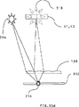
図1aは、ディスプレイ平面1の表示面の平面図を示す。右眼2は、ディスプレイ平面上の右眼相同像点(homologous image point)3を見ており、左眼4は、ディスプレイ平面上の左眼相同像点5を見ており、それにより、スクリーン平面の後方にユーザが認識する見かけ上の像点6が生成される。
FIG. 1 a shows a plan view of the display surface of the
図1bは、ディスプレイ平面1の表示面の平面図を示す。右眼2は、ディスプレイ平面上の右眼相同像点7を見ており、左眼4は、ディスプレイ平面上の左眼相同像点8を見ており、それにより、スクリーン平面の前方に見かけ上の像点9が生成される。
FIG. 1 b shows a plan view of the display surface of the
図1cは、左眼画像10および右眼画像11の外観を示す。左眼画像10の相同点5は、基準線12上に位置決めされる。右眼画像11の対応する相同点3は、基準線12に対して異なる相対位置3にある。基準線12からの点3の間隔13は、視差(disparity)と呼ばれ、この場合、スクリーン平面の後方にある点の正の視差(positive disparity)である。
FIG. 1 c shows the appearance of the
シーンにおける一般的な点に関して、図1aに示すようなステレオペアの各像には対応する点がある。これらの点は相同点と呼ばれる。2つの像の間の相同点の相対間隔は視差と呼ばれ、視差がゼロになる点は、ディスプレイの奥行き面(depth plane)の点に対応する。図1bは、非交差性視差を有する点がディスプレイの後方に現れることを示し、図1cは、交差性視差を有する点がディスプレイの前方に現れることを示す。相同点の間隔、観察者までの距離、および観察者の眼間距離の大きさにより、ディスプレイで認識される奥行きの程度が決まる。 With respect to general points in the scene, there is a corresponding point in each image of a stereo pair as shown in FIG. These points are called homologous points. The relative spacing of the homologous points between the two images is called parallax, and the point where the parallax is zero corresponds to a point on the depth plane of the display. FIG. 1b shows that a point with non-crossing parallax appears behind the display, and FIG. 1c shows that a point with crossing parallax appears in front of the display. The degree of depth recognized on the display is determined by the distance between the homologous points, the distance to the observer, and the size of the distance between the eyes of the observer.
立体型ディスプレイは、従来技術において既知であり、ユーザがある種類の視認補助具を装着して、左右の眼に送られるビューを実質的に分離するようにするディスプレイを指す。例えば、視認補助具は、画像が(例えば赤色および緑色に)色分けされるカラーフィルタ、画像が直交偏光状態で符号化される偏光眼鏡、またはビューが眼鏡のシャッタの開放と同期して画像の時間的配列として符号化されるシャッタ眼鏡であってもよい。 A stereoscopic display is known in the prior art and refers to a display in which a user wears a type of visual aid to substantially separate the views sent to the left and right eyes. For example, the visual aid is a color filter in which the image is color-coded (for example, red and green), polarized glasses in which the image is encoded in an orthogonal polarization state, or the time of the image synchronized with the opening of the shutter of the glasses. It may be shutter glasses encoded as a target array.
自動立体ディスプレイは、観察者が視認補助具を装着しなくても動作する。自動立体ディスプレイでは、図2に示すように、空間内の限られた領域からビューのそれぞれを見ることができる。 The autostereoscopic display operates even when an observer does not wear a visual aid. In the autostereoscopic display, as shown in FIG. 2, each of the views can be viewed from a limited area in the space.
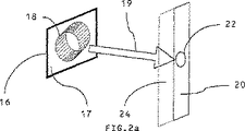
図2aは、パララックス(parallax)光学素子17が取り付けられた表示デバイス16を示す。表示デバイスは、右眼チャネルとして右眼画像18を生成する。パララックス光学系17は、矢印19で示される方向に光を導き、ディスプレイの前方の領域に右眼観察ウィンドウ20を生成するようにする。観察者は、自身の右眼22をウィンドウ20の位置に位置付ける。左眼観察ウィンドウ24の位置を参照のために示す。観察ウィンドウ20は、垂直方向に延びた光学瞳とも呼ばれる。
FIG. 2a shows a
図2bは、左眼光学系を示す。表示デバイス16は、左眼チャネルとして左眼画像26を生成する。パララックス光学系17は、矢印28で示される方向に光を導き、ディスプレイの前方の領域に左眼観察ウィンドウ30を生成するようにする。観察者は、自身の左眼32をウィンドウ30の位置に位置付ける。右眼観察ウィンドウ20の位置を参照のために示す。
FIG. 2b shows the left eye optical system. The
本システムは、ディスプレイと光学的方向制御機構(optical steering mechanism)とを備える。左画像26からの光は、観察ウィンドウ30と呼ばれるディスプレイの前方の限られた領域に送られる。眼32が観察ウィンドウ30の位置に位置付けられている場合、観察者にはディスプレイ16の全体にわたって適切な画像26が見える。同様に、光学系は、右画像18用に意図された光を別個のウィンドウ20に送る。観察者が自身の右眼22をウィンドウ20に位置付けている場合、右眼画像はディスプレイの全体にわたって見られる。概して、いずれの画像からの光も、各指向性分布(directional distribution)に光学的に方向制御された(ずなわち、導かれた)ものと考えられてよい。
The system includes a display and an optical steering mechanism. Light from the
図3は、ウィンドウ平面42に左眼観察ウィンドウ36、37、38および右眼観察ウィンドウ39、40、41を生成する、ディスプレイ平面34における表示デバイス16、17の平面図を示す。ディスプレイからのウィンドウ平面の間隔は、公称視距離43と呼ばれる。ディスプレイに関して中央の位置にあるウィンドウ37、40は、ゼロ番ローブ44にある。ゼロ番ローブ44の右側にあるウィンドウ36、39は、+1番ローブ46にあり、ゼロ番ローブの左側にあるウィンドウ38、41は、−1番ローブ48にある。
FIG. 3 shows a plan view of the
ディスプレイの観察ウィンドウ平面は、横方向の観察自由度が最大となるディスプレイからの距離を表す。図3の平面図に示すように、ウィンドウ平面から離れた地点には、ダイヤモンド形の自動立体観察ゾーンがある。図に見られるように、ディスプレイにわたる点それぞれからの光は、有限幅を有する円錐形で観察ウィンドウに放たれる。円錐の幅は、角度幅として定義されてよい。 The observation window plane of the display represents the distance from the display that maximizes the degree of freedom of observation in the horizontal direction. As shown in the plan view of FIG. 3, there is a diamond-shaped autostereoscopic observation zone at a point away from the window plane. As can be seen in the figure, light from each point across the display is emitted into the viewing window in a cone shape with a finite width. The width of the cone may be defined as the angular width.
一対の観察ゾーン、例えば37、40のそれぞれに眼が位置付けられている場合、自動立体画像はディスプレイの全範囲にわたって見える。一次的には、ディスプレイの縦方向の観察自由度は、これらの観察ゾーンの長さにより決まる。 If the eye is positioned in each of a pair of viewing zones, eg 37, 40, the autostereoscopic image is visible over the entire range of the display. First, the viewing freedom in the vertical direction of the display is determined by the length of these viewing zones.
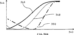
図4aでは、ディスプレイのウィンドウ平面全体の強度50の変動(1つの有形形態の光の指向性分布を構成する)を、理想的なウィンドウの場合の位置51に関して示す。右眼ウィンドウ位置の強度分布52は図3のウィンドウ41に対応し、強度分布53はウィンドウ37に対応し、強度分布54はウィンドウ40に対応し、強度分布55はウィンドウ36に対応する。
In FIG. 4a, the variation of
図4bは、より現実的なウィンドウの場合の位置での強度分布を概略的に示す。右眼ウィンドウ位置の強度分布56は図3のウィンドウ41に対応し、強度分布57はウィンドウ37に対応し、強度分布58はウィンドウ40に対応し、強度分布59はウィンドウ36に対応する。
FIG. 4b schematically shows the intensity distribution at the position for a more realistic window. The
図4に示すように、画像の分離品質(quality)、およびディスプレイの横方向および縦方向の観察自由度の大きさは、ウィンドウの品質により決まる。図4aは、理想的な観察ウィンドウを示すが、図4bは、ディスプレイから出力され得る実際の観察ウィンドウの概略図である。ウィンドウ性能が不十分であることにより、いくつかのアーチファクト(artefact)が生じる可能性がある。右眼画像からの光を左眼で見た場合、およびその反対の場合、クロストークが生じる。これは、ユーザにとって視覚的歪みをもたらす可能性がある重要な3D画像劣化のメカニズムである。さらに、ウィンドウの品質が悪いと、観察者の観察自由度が低下することになる。本光学系は、観察ウィンドウの性能を最適化するように設計される。 As shown in FIG. 4, the quality of image separation and the degree of freedom of observation in the horizontal and vertical directions of the display are determined by the quality of the window. FIG. 4a shows an ideal viewing window, while FIG. 4b is a schematic view of an actual viewing window that can be output from the display. Insufficient window performance can cause some artifacts. Crosstalk occurs when light from the right eye image is viewed with the left eye and vice versa. This is an important 3D image degradation mechanism that can cause visual distortion for the user. Furthermore, if the quality of the window is poor, the observer's degree of freedom of observation will decrease. The optical system is designed to optimize the performance of the observation window.
パララックスバリアディスプレイ
図5の平面図に示すように、既知のフラットパネル型の自動立体ディスプレイのあるタイプのものは、バックライトと、列および行をなして配列された電子的に調整可能な画素のアレイ(空間光変調器、SLMとして知られている)と、ディスプレイの前部に取り付けられたパララックスバリアとを備える。
Parallax Barrier Display As shown in the plan view of FIG. 5, one type of known flat panel autostereoscopic display is a backlight and electronically adjustable pixels arranged in columns and rows. Array (known as a spatial light modulator, SLM) and a parallax barrier attached to the front of the display.
バックライト60は光出力62を生成し、光出力62はLCD入力偏光子64に入射する。光はTFT LCD基板66を透過し、LCD画素平面67に列および行をなして配列された画素の反復アレイ(repeating array)に入射する。赤色画素68、71、73、緑色画素69、72、75、および青色画素70、73はそれぞれ、個別に制御可能な液晶層を構成し、ブラックマスク76と呼ばれる不透明マスクの領域により分離される。各画素は、透過領域、すなわち画素開口78を含む。画素を通過する光は、LCD画素平面74の液晶材料により位相が変調され、LCDカラーフィルタ基板80に配置されたカラーフィルタにより色が変調される。次に、光は出力偏光子82を通過し、その後、パララックスバリア84およびパララックスバリア基板86に到達する。パララックスバリア84は、垂直方向に延びた不透明領域により分離された、垂直方向に延びた透過領域のアレイを含み、画素69からの光の光線88で示されるように、1つおきの画素列69、71、73、75からの光を右眼へと導き、光線90で示されるように、その間の列68、70、72、74からの光を左眼へと導く役割を果たす(この光方向パターン全体が、光の指向性分布の別の例となる)。観察者には、バリアの開口92を照明する、下にある画素からの光が見える。
The
本明細書では、SLMは、液晶ディスプレイなどの「光弁」デバイスと、エレクトロルミネッセンスディスプレイおよびLEDディスプレイなどの発光型デバイス(emissive devices)との両方を含む。 As used herein, an SLM includes both “light valve” devices such as liquid crystal displays and emissive devices such as electroluminescent and LED displays.
ディスプレイの画素は、ギャップ(通常は液晶ディスプレイ、すなわちLCDのブラックマスクにより画定される)により分離された行および列として配列され、画素列のピッチの2倍に近いピッチの垂直方向に延びたスリットのアレイであるパララックスバリアを有する。パララックスバリアは、各画素列からの光を見ることができる角度の範囲を制限し、これにより、ディスプレイの前方の領域に観察ウィンドウを生成する。ディスプレイからの出力円錐の角度は、画素開口の幅および形状と、パララックスバリアの配向(alignment)および収差とによって決まる。 The pixels of the display are arranged as rows and columns separated by gaps (usually defined by the liquid crystal display, ie, the black mask of the LCD), and vertically extending slits with a pitch close to twice the pitch of the pixel columns A parallax barrier which is an array of The parallax barrier limits the range of angles through which light from each pixel column can be viewed, thereby creating an observation window in the area in front of the display. The angle of the output cone from the display is determined by the width and shape of the pixel aperture and the alignment and aberration of the parallax barrier.
各画素から観察ウィンドウまで光を方向制御するために、パララックスバリアのピッチは画素アレイのピッチの2倍よりもわずかに小さい。この条件は「視点補正」として知られる。このようなディスプレイにおいて、ステレオペア像の各々の水平解像度はベースLCDの半分であり、2つのビューが生成される。 In order to direct the light from each pixel to the observation window, the pitch of the parallax barrier is slightly smaller than twice the pitch of the pixel array. This condition is known as “viewpoint correction”. In such a display, the horizontal resolution of each stereo pair image is half that of the base LCD, and two views are generated.
したがって、奇数列の画素68、70、72、74からの光は、左の観察ウィンドウから見ることができ、偶数列の画素69、71、73、75からの光は、右の観察ウィンドウから見ることができる。左眼画像データがディスプレイの奇数列に位置付けられ、右眼画像データが偶数列に位置付けられる場合、正確な「正像(orthoscopic)」位置にいる観察者は、ディスプレイ全体の自動立体3D画像を見るために2つの画像を融合せねばならない。
Thus, light from odd columns of
2つのビューの間には、左眼のビューのいくらかが右眼で見えるような、またはその反対であるような光の漏れ(light leakage)があるであろう。この漏れは画像のクロストークと呼ばれる。クロストークは、3Dディスプレイを見る際の視覚歪みをもたらす重要なメカニズムであり、それを制御することが3Dディスプレイの開発の主な原動力である。フラットパネル型の自動立体ディスプレイ(特に、LCD技術に基づいたもの)では、ウィンドウの性能に対する制限は通常、画素の形状および開口率と光学要素の品質によって決まる。 There will be light leakage between the two views such that some of the left eye view is visible to the right eye, or vice versa. This leakage is called image crosstalk. Crosstalk is an important mechanism that causes visual distortion when viewing a 3D display, and controlling it is the main driving force in the development of 3D displays. In flat panel autostereoscopic displays (especially those based on LCD technology), limitations on window performance are usually determined by pixel shape and aperture ratio and optical element quality.
パララックスバリアタイプのディスプレイでは、スリットの直下にある画素列は、ディスプレイのゼロ番ローブにある第1の対のウィンドウに結像される。隣接する画素列もまた、ディスプレイの+1番および−1番ローブにある観察ウィンドウに結像される。したがって、図3に見られるように、ユーザが正像ゾーンから横方向に外れた場合、不正確な画像からの光が各眼に送られることになる。右眼が左眼用ビューを見ている場合、またはその反対の場合、その画像は、正確な正像状態と比較して、「擬似像(pseudoscopic)」と呼ばれる。 In a parallax barrier type display, the pixel column immediately below the slit is imaged in a first pair of windows in the zeroth lobe of the display. Adjacent pixel columns are also imaged in the viewing window in the +1 and -1 lobes of the display. Therefore, as seen in FIG. 3, if the user moves laterally away from the normal image zone, light from an inaccurate image will be sent to each eye. If the right eye is looking at the left-eye view, or vice versa, the image is referred to as a “pseudoscopic” compared to the correct normal state.
ディスプレイの横方向の観察自由度を拡大するために、2つ以上の画素列をバリアの各スリットの下に配置することができる。例えば、4つの列の場合、ビューが各ウィンドウごとに変わる4つのウィンドウが形成される。このようなディスプレイでは、観察者が動くと「見回す」ように見ることができる。縦方向の自由度も、このような方法によって増加する。しかしながら、この場合、ディスプレイの解像度はベースパネルの解像度の1/4に制限される。 In order to increase the viewing flexibility in the lateral direction of the display, two or more pixel columns can be placed under each slit in the barrier. For example, in the case of four columns, four windows are formed where the view changes for each window. Such a display can be seen as “look around” as the observer moves. The degree of freedom in the vertical direction is also increased by such a method. However, in this case, the display resolution is limited to ¼ of the base panel resolution.
パララックスバリアは、ディスプレイの領域から光を遮ることに頼っているため、輝度およびデバイスの効率は通常、元のディスプレイの輝度の約20〜40%に低下する。 Since the parallax barrier relies on blocking light from the display area, the brightness and device efficiency are typically reduced to about 20-40% of the original display brightness.
ディスプレイの画素構造に関してバリアのサブピクセル配向許容度の要件があるため、ディスプレイの観察自由度を最適化するために、パララックスバリアが容易に取り外しおよび交換されることはない。2Dモードの解像度は半分である。 Due to the requirements of the sub-pixel orientation tolerance of the barrier with respect to the pixel structure of the display, the parallax barrier is not easily removed and replaced to optimize the viewing freedom of the display. The resolution in 2D mode is half.
パララックスバリアの光学構成要素
パララックスバリア要素が表示デバイスの前方に位置付けられるようなパララックスバリアディスプレイのあるタイプのものは、T. Okoshiによる「Three Dimensional Imaging Techniques」(Academic Press 1976)に開示されている。
Parallax Barrier Optical Components One type of parallax barrier display in which the parallax barrier element is positioned in front of a display device is disclosed in “Three Dimensional Imaging Techniques” (Academic Press 1976) by T. Okoshi. ing.
別のタイプのパララックスバリアディスプレイでは、G. Hamagishi等著「A Display System with 2D/3D compatibility」(Proc. SID 1998 pp915-918)に開示されるように、パララックス素子はディスプレイの後方のスリットとして具現されてよい。このようなディスプレイでは、フレネル回折のアーチファクトが生じ、得ることができる観察ウィンドウの品質が制限されることを示すことができる。 In another type of parallax barrier display, as disclosed in “A Display System with 2D / 3D compatibility” by G. Hamagishi et al. (Proc. SID 1998 pp915-918), the parallax element is a slit behind the display. It may be embodied as In such a display, Fresnel diffraction artifacts can occur, indicating that the quality of the viewing window that can be obtained is limited.
別のタイプのパララックスバリアディスプレイでは、米国特許第4,717,949号に開示されるように、パララックス素子は暗い領域が点在している光のラインとして具現されてもよい。このようなディスプレイでは、フレネル回折のアーチファクトが生じ、得ることができる観察ウィンドウの品質が制限されることが示される(G. Woodgate等著「Flat panel autostereoscopic displays - characterisation and enhancement」Proc SPIE, Vol 3957, pp153-164, 2000)。 In another type of parallax barrier display, as disclosed in US Pat. No. 4,717,949, parallax elements may be embodied as lines of light interspersed with dark areas. Such displays have been shown to produce Fresnel diffraction artifacts and limit the quality of the viewing window that can be obtained (G. Woodgate et al. “Flat panel autostereoscopic displays-characterisation and enhancement” Proc SPIE, Vol 3957 , pp153-164, 2000).
レンチキュラーディスプレイ
立体ディスプレイ(stereoscopic displays)で用いるものとして当該技術分野において既知のパララックス光学系(パララックスバリアを参照)の別のタイプのものは、レンチキュラースクリーンと呼ばれており、これは垂直方向に延びた円柱マイクロレンズのアレイである。本明細書中で用いる「円柱」という用語は、当該技術分野において通常の意味を有し、厳密に球面レンズ形状だけではなく非球面レンズ形状も含む。レンズのピッチは、ここでも視点補正条件に対応する。レンズの曲率は、ウィンドウ平面においてLCD画素の画像を生成するように実質的に設定される。レンズが画素から円錐形の光を集光し、それをウィンドウに分配するため、レンチキュラーディスプレイはベースパネルのフル輝度を有する。
Lenticular Display Another type of parallax optical system (see parallax barrier) known in the art for use in stereoscopic displays is called a lenticular screen, which is vertically oriented. It is an array of extended cylindrical microlenses. As used herein, the term “cylinder” has its usual meaning in the art and includes not only strictly spherical lens shapes but also aspheric lens shapes. The lens pitch again corresponds to the viewpoint correction condition. The curvature of the lens is substantially set to produce an image of the LCD pixel in the window plane. Since the lens collects conical light from the pixels and distributes it to the window, the lenticular display has the full brightness of the base panel.
図6は、従来技術のレンチキュラーディスプレイデバイスの構造を示す。デバイスは、出力偏光子82までは図5に記載したものと同様の構成である。次に、光は、レンチキュラースクリーン基板94と、レンチキュラースクリーン基板92の表面に形成されたレンチキュラースクリーン96とを通過する。パララックスバリアに関しては、レンチキュラースクリーン94が、画素69からの光線88で示されるように、1つおきの画素列69、71、73、75からの光を右眼へと導き、画素68からの光線90で示されるように、その間の列68、70、72、74からの光を左眼へと導くのに役立つ。観察者には、レンチキュラースクリーン96の個々のレンチクル98の開口を照明する、下にある画素からの光が見える。取り込まれた光円錐の大きさは、取り込まれた光線100により示される。
FIG. 6 shows the structure of a prior art lenticular display device. The device has the same configuration as that described in FIG. 5 up to the
レンチキュラーディスプレイは、T. Okoshi著「Three Dimensional Imaging Techniques」(Academic Press, 1976)に記載されている。空間光変調器を用いるあるタイプのレンチキュラーディスプレイは、米国特許第4,959,641号に記載されている。米国特許第4,959,641号の発明は、空中での(in air)非切り替えレンチキュラー要素を説明している。 Lenticular displays are described in “Three Dimensional Imaging Techniques” by A. Okoshi (Academic Press, 1976). One type of lenticular display that uses a spatial light modulator is described in US Pat. No. 4,959,641. U.S. Pat. No. 4,959,641 describes a non-switching lenticular element in air.
このようなディスプレイでは、レンズ96およびその付近への反射および散乱によるレンズ表面の望ましくない可視化が生じ、これが画像のコントラストを低下させる可能性がある。反射は、例えばフレネル反射によるものであろう。
In such displays, undesirable visualization of the lens surface due to reflection and scattering to and from the
観察自由度の拡大
上述のフラットパネルディスプレイの観察自由度は、ディスプレイのウィンドウ構造により制限される。
Expansion of viewing freedom The viewing freedom of the flat panel display described above is limited by the window structure of the display.
観察自由度が観察者の位置の測定およびそれに応じたパララックス素子の移動により改善されるディスプレイが、欧州特許第0829743号に記載されている。このような観察者測定装置および機械的作動は、高価かつ複雑である。 A display in which the degree of freedom of observation is improved by measuring the position of the observer and the movement of the parallax element accordingly is described in EP 0829743. Such observer measurement devices and mechanical actuation are expensive and complex.
ウィンドウの光学構造が変化せず(例えば固定パララックス光学ディスプレイ)、画像データが観察者の測定位置に応じて切り替えられて、観察者がほぼ立体的な画像を維持するようにするディスプレイが、例えば欧州特許第0721131号に記載されている。 A display that does not change the optical structure of the window (e.g. a fixed parallax optical display) and the image data is switched according to the measurement position of the observer so that the observer maintains a substantially stereoscopic image, e.g. It is described in EP0721131.
正確な観察位置を設定するためのインジケータ
観察者が自身の最適な位置を特定することができるようにするためのインジケータが実装されているディスプレイが、「Proceedings of Third International Display Workshop」(volume 2, November 27-29, 1996 E. Nakayama等著, 1996 International Conference Centre, Kobe, Japan)に記載されている。このようなインジケータは、観察者の縦方向の位置に関する情報も、観察者の横方向の位置に関する正確な情報も与えない。
Indicator for setting the correct observation position The display that implements the indicator to enable the observer to identify his / her best position is called “Proceedings of Third International Display Workshop” (
別のタイプのインジケータ[欧州特許第0860728号]は、イメージディスプレイと、信号ディスプレイと、イメージディスプレイと協働して観察領域の複数の右眼および左眼観察ゾーンを形成する部分、ならびに信号ディスプレイと協働して、観察領域の少なくとも1つの第1の部分で可視の第1の信号画像および観察領域の少なくとも1つの第2の部分で可視の第2の信号画像を形成する第2の部分、を有するパララックス光学系を用いる。このようなインジケータは、表示面積の一部を用いるため、有効な画像面積が制限される。これは小さいディスプレイにとって特に不利であるが、それは、インジケータの高さが(ユーザにとっての可視性を維持する)ディスプレイのサイズに合わせられておらず、これに比例して小さいディスプレイのより大きい面積が覆われてしまうからである。さらに、解像度がいくらか損なわれるため、3D表示面積が、例えばVGA(640×3×480画素)などの標準的な画像面積ではなくなる。 Another type of indicator [European Patent No. 0860728] includes an image display, a signal display, a portion that cooperates with the image display to form a plurality of right and left eye viewing zones in the viewing area, and a signal display. In cooperation, a second part forming a first signal image visible in at least one first part of the observation area and a second signal image visible in at least one second part of the observation area; A parallax optical system having Since such an indicator uses a part of the display area, an effective image area is limited. This is particularly disadvantageous for small displays, but it does not match the height of the indicator to the size of the display (maintaining visibility to the user) and the proportionally larger area of the small display Because it will be covered. Furthermore, since the resolution is somewhat lost, the 3D display area is no longer a standard image area such as VGA (640 × 3 × 480 pixels).
さらに、欧州特許第0860728号では、透過型ディスプレイとともに用いた場合、反射された周辺光を用いてインジケータを照明することができない。欧州特許第0860728号はまた、単一部分としてインジケータ部分の輝度を高めるために、ディスプレイのカラーフィルタを交換せねばならないことを教示している。これには、LCD製造プロセスへの変更が必要であり、その結果、ディスプレイの一部が永久に失われることになる可能性がある。 Further, in EP 0 860 728, when used with a transmissive display, the indicator cannot be illuminated with reflected ambient light. EP 0 860 728 also teaches that the color filter of the display must be replaced in order to increase the brightness of the indicator part as a single part. This requires a change to the LCD manufacturing process, which can result in permanent loss of part of the display.
2D−3D切り替え可能ディスプレイ
上述のように、空間的に多重化された3D表示を生成するためのパララックス光学系の使用により、各画像の解像度はフル表示解像度のせいぜい半分に制限される。多くの用途でディスプレイは、わずかな時間だけ3Dモードで用いることが意図され、フル解像度でアーチファクトのない2Dモードを有することが必要とされる。
2D-3D Switchable Display As described above, the use of parallax optics to generate spatially multiplexed 3D displays limits the resolution of each image to at most half of the full display resolution. In many applications, the display is intended to be used in 3D mode for only a short time and is required to have 2D mode with full resolution and no artifacts.
パララックス光学系の効果が除去されるあるタイプのディスプレイは、Proc.SPIE vol. 1915 Stereoscopic Displays and Applications IV (1993)pp177-186「Developments In Autostereoscopic Technology at Dimension Technologies Inc.」, 1993に開示されている。この場合、切り替え可能ディフューザ素子が、光のラインを形成するために用いられる光学系に配置される。このような切り替え可能ディフューザは、例えば、高分子分散型液晶タイプのものであってよく、これは、材料にわたって印加電圧を適用することにより、分子配列が散乱モードと非散乱モードとの間で切り替わるものである。3Dモードでは、ディフューザはクリアであり、後方パララックスバリア効果(rear parallax barrier effect)をもたらすために光のラインが生成される。2Dモードでは、ディフューザは散光性であり(scattering)、光のラインが消滅し(washed out)、均一光源の効果がもたらされる。このように、ディスプレイの出力は実質的に均等拡散(Lambertian)であり、ウィンドウが消滅する。すると、観察者にはディスプレイがフル解像度の2Dディスプレイとして見える。このようなディスプレイでは、3Dモードでフレネル回折アーチファクトが生じ、またディフューザのクリアな状態で望ましくない残留散乱が生じ、これがディスプレイのクロストークを増加させる。したがって、このようなディスプレイは高レベルの視覚的歪みを示す可能性が高い。 One type of display that eliminates the effects of parallax optics is disclosed in Proc. SPIE vol. 1915 Stereoscopic Displays and Applications IV (1993) pp 177-186 “Developments In Autostereoscopic Technology at Dimension Technologies Inc.”, 1993. Yes. In this case, the switchable diffuser element is arranged in an optical system used to form a light line. Such a switchable diffuser may be of the polymer dispersed liquid crystal type, for example, which switches the molecular arrangement between scattering and non-scattering modes by applying an applied voltage across the material. Is. In 3D mode, the diffuser is clear and a line of light is created to provide a rear parallax barrier effect. In the 2D mode, the diffuser is scattering and the light lines are washed out, resulting in the effect of a uniform light source. Thus, the output of the display is substantially Lambertian and the window disappears. The viewer will then see the display as a full resolution 2D display. In such displays, Fresnel diffraction artifacts occur in 3D mode, and undesirable residual scattering occurs in the clear state of the diffuser, which increases display crosstalk. Thus, such a display is likely to exhibit a high level of visual distortion.
別のタイプの切り替え可能2D−3Dディスプレイ[例えば、欧州特許第0833183号]では、第2のLCDがディスプレイの前部に配置されて、パララックス光学系としての役割を果たす。第1のモードでは、パララックスLCDはクリアであるため、ウィンドウが形成されず、画像は2Dで見られる。第2のモードでは、パララックスバリアのスリットを生成するようにデバイスが切り替えられる。次に、出力ウィンドウが形成され、画像が3Dに見える。このようなディスプレイは、2つのLCD素子の使用によりコストおよび複雑性が増すとともに、輝度が低下するか、または消費電力が増す。反射モードの3D表示システムで用いる場合、パララックスバリアは、光をディスプレイに入る途中およびディスプレイから出る途中の両方でパララックスバリアの遮断領域により減衰させるために、非常に低い輝度をもたらす。 In another type of switchable 2D-3D display [e.g. EP 0833183], a second LCD is placed in front of the display and serves as a parallax optic. In the first mode, the parallax LCD is clear, so no window is formed and the image is viewed in 2D. In the second mode, the device is switched to create a parallax barrier slit. Next, an output window is formed and the image looks 3D. Such displays have increased cost and complexity due to the use of two LCD elements, with reduced brightness or increased power consumption. When used in a reflective mode 3D display system, the parallax barrier provides very low brightness because light is attenuated by the blocking region of the parallax barrier both on entering and exiting the display.
別のタイプの切り替え可能2D−3Dディスプレイ[欧州特許第0829744号]では、パララックスバリアは、半波長リターダ素子(half-wave retarder elements)のパターン化されたアレイを含む。リターダ素子のパターンは、パララックスバリア素子のバリアスリットおよび吸収領域のパターンに対応する。3D動作モードでは、偏光子がディスプレイに加えられることにより、パターン化されたリターダのスリットを通る光が検査(analyze)される。このようにして吸収パララックスバリアが生成される。2D動作モードでは、2D動作モードにはいかなる偏光特性も関与しないため、偏光子は完全に取り外される。したがって、ディスプレイの出力はフル解像度およびフル輝度である。1つの欠点は、このようなディスプレイはパララックスバリア技術を用いるため、3D動作モードではおそらく20〜30%の輝度に制限されることである。また、ディスプレイは、バリアの開口からの回折により制限される観察自由度およびクロストークを有することになる。 In another type of switchable 2D-3D display [European Patent No. 0 809 744], the parallax barrier includes a patterned array of half-wave retarder elements. The pattern of the retarder element corresponds to the pattern of the barrier slit and the absorption region of the parallax barrier element. In the 3D mode of operation, a polarizer is added to the display to analyze the light passing through the slits of the patterned retarder. In this way, an absorption parallax barrier is generated. In the 2D mode of operation, the polarizer is completely removed because no polarization properties are involved in the 2D mode of operation. Accordingly, the output of the display is full resolution and full brightness. One disadvantage is that such displays use parallax barrier technology and are therefore limited to 20-30% brightness in 3D mode of operation. The display will also have viewing freedom and crosstalk limited by diffraction from the barrier opening.
光の方向を切り替えるために、電気的に切り替え可能な複屈折レンズを設けることが知られている。このようなレンズを用いて、ディスプレイを2D動作モードと3D動作モードとの間で切り替えることが知られている。 In order to switch the direction of light, it is known to provide an electrically switchable birefringent lens. It is known to switch the display between 2D and 3D operation modes using such a lens.
例えば、電気的に切り替え可能な複屈折液晶マイクロレンズが、European Optical Society Topical Meetings Digest Series: 13, 15-16 May 1997 L. G. Commander等著、「Electrode designs for tuneable microlenses」(pp48-58)に記載されている。 For example, an electrically switchable birefringent liquid crystal microlens is described in “Electrode designs for tuneable microlenses” (pp48-58) by the European Optical Society Topical Meetings Digest Series: 13, 15-16 May 1997 LG Commander et al. ing.
別のタイプの切り替え可能2D−3Dディスプレイ[米国特許第6,069,650号、WO98/21620]では、液晶材料で充填されたレンチキュラースクリーンを含む切り替え可能マイクロレンズが、レンチキュラースクリーンの光パワーを変えるために用いられる。 In another type of switchable 2D-3D display [US Pat. No. 6,069,650, WO 98/21620], a switchable microlens that includes a lenticular screen filled with a liquid crystal material changes the optical power of the lenticular screen. Used for.
液晶フレネルレンズを含む3Dディスプレイが、S. Suyam等著「3D Display System with Dual Frequency Liquid Crystal Varifocal Lens」、SID 97 DIGEST pp273-276に記載されている。 A 3D display including a liquid crystal Fresnel lens is described in S. Suyam et al., “3D Display System with Dual Frequency Liquid Crystal Varifocal Lens”, SID 97 DIGEST pp273-276.
例えばより多くの光を蓄える際にバリアではなくレンズを用いることが有利であり得るが、切り替え可能レンズを含む上述の2D−3Dディスプレイは、いくつかの欠点を有する。例えば、Commander等による参考文献の電気的に切り替え可能な複屈折液晶マイクロレンズの場合、マイクロレンズの光学特性は、切り替えられていない残りの液晶および隣接するマイクロレンズのカスプ付近で生じるディスクリネーションにより制限される。 For example, it may be advantageous to use a lens rather than a barrier to store more light, but the 2D-3D display described above that includes a switchable lens has several drawbacks. For example, in the case of an electrically switchable birefringent liquid crystal microlens in a reference by Commander et al., The optical characteristics of the microlens are due to the remaining liquid crystal that has not been switched and the disclination that occurs near the cusp of the adjacent microlens. Limited.
液晶材料の温度による屈折率の変動は、レンズの焦点距離が変わることを意味する。したがって、このようなディスプレイは、温度制御しなければ、限られた動作温度範囲を有することになる。さらに、レンズの表面には電極材料が堆積されることが必要である。このことにより、2D動作モードおよび3D動作モードの両方での画像のコントラストを低下させる散乱反射が生じる。特にレンズ側の配向特性は、素子の寿命の間は、時間、温度、および物理的応力に対して維持される必要がある。 A change in refractive index due to the temperature of the liquid crystal material means that the focal length of the lens changes. Therefore, such a display will have a limited operating temperature range if it is not temperature controlled. Furthermore, electrode material needs to be deposited on the surface of the lens. This results in scattered reflections that reduce the contrast of the image in both 2D and 3D operation modes. In particular, the orientation properties on the lens side need to be maintained over time, temperature, and physical stress during the lifetime of the element.
別の例として、米国特許第6,069,650号およびWO98/21620に開示されるディスプレイの場合、マイクロレンズの光学性能は、上述のように、レンチキュラースクリーンの切り替えられていない領域のために制限されるであろう。したがって、2Dにいくらかのレンズ機能が残っており、これがウィンドウ平面にいくらかの強度変化をもたらす可能性があり、同様に、3Dモードにいくらかの非レンズ機能が残っており、これがディスプレイのクロストークを増加させる可能性がある。 As another example, for the displays disclosed in US Pat. No. 6,069,650 and WO 98/21620, the optical performance of the microlens is limited by the unswitched area of the lenticular screen, as described above. Will be done. Therefore, some lens functionality remains in 2D, which can cause some intensity change in the window plane, and similarly, some non-lens functionality remains in 3D mode, which can cause crosstalk on the display. There is a possibility to increase.
2Dディスプレイに関する複屈折レンズ
様々な無関係な用途のために、ディスプレイにおいて複屈折レンズを用いることは知られており、その用途としては例えば以下のものが挙げられる。
Birefringent lenses for 2D displays It is known to use birefringent lenses in displays for a variety of unrelated applications, including, for example:
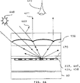
LCDプロジェクタの用途のための複屈折マイクロレンズが、公開特許英文抄録(Patent Abstracts of Japan)の特開平11−271744に記載されている。当該システムの入力照明構造を図7に示す。ディレクタ方向104を有する複屈折マイクロレンズ102のアレイが、液晶層106と、赤色データ画素110、緑色データ画素112、および青色データ画素114を含む反射画素108のアレイとの上に配置される。ディスプレイは、赤色画素には第1の方向116から、緑色画素には第2の方向118から、青色画素には第3の方向120から照明される。照明偏光方向124は、等方性材料126に浸漬されたレンズの異常光屈折率104に平行である。
A birefringent microlens for use in an LCD projector is described in Japanese Patent Application Laid-Open No. 11-271744 in Patent Abstracts of Japan. The input illumination structure of the system is shown in FIG. An array of
特開平11−271744の単色画素の照明を図8に示す。偏光状態124を有する入力光線118とほぼ同一方向に向いた入力照明円錐が、レンズ102により画素112上に集束される。光はLC層106により変調され、画素112により反射されて、それにより、入力偏光状態124と直交する偏光成分128を有するようになる。出力光線130が生成されて、固定ビームスプリッティング構成要素(図示せず)および投影レンズ(図示せず)により集光され、投影スクリーン(図示せず)に向けられる。
FIG. 8 shows illumination of a single color pixel disclosed in Japanese Patent Laid-Open No. 11-271744. An input illumination cone oriented in approximately the same direction as the
複屈折マイクロレンズのアレイを備えたLCDパネルは、赤色、緑色、青色の光からなる直線偏光された別個の円錐により照明される。複屈折レンズを取り巻く材料は、複屈折材料の遅相軸とほぼ同じ屈折率を有する。レンズの材料の複屈折の進相軸は、レンズを通る入力直線偏光が分解される(the lens is analyzed by the input linear polarization)ように構成される。したがって、レンズの動作により、緑色光は緑色画素に、赤色光は赤色画素に、青色光は青色画素に送られる。反射の際には、投影スクリーンに送られるのに有効な光は直交偏光状態である。この出力偏光状態は、屈折率が整合した複屈折マイクロレンズの遅相軸に一致する(see)ため、レンズを通る光は分解されない。このように、ディスプレイの出力はマイクロレンズの開口による光量低下を受けず(not vignetted)、デバイスからの光の完全な円錐が、投影レンズにより集光され得る。このようなデバイスは、単一の反射型LCDパネルから効率的に光を照射および集光して、低コストおよび高輝度の投影システムをもたらすことができる。このようなデバイスは、指向性表示システムでは用いられず、複屈折レンズが切り替え可能である結果でもない。 An LCD panel with an array of birefringent microlenses is illuminated by a separate linearly polarized cone of red, green and blue light. The material surrounding the birefringent lens has approximately the same refractive index as the slow axis of the birefringent material. The fast axis of birefringence of the lens material is configured such that the lens is analyzed by the input linear polarization. Therefore, by the operation of the lens, green light is sent to the green pixel, red light is sent to the red pixel, and blue light is sent to the blue pixel. Upon reflection, the light that is effective to be sent to the projection screen is in the orthogonal polarization state. This output polarization state (see) matches the slow axis of the birefringent microlens with matched refractive index, so that light passing through the lens is not decomposed. In this way, the output of the display is not vignetted by the aperture of the microlens and a complete cone of light from the device can be collected by the projection lens. Such a device can efficiently illuminate and collect light from a single reflective LCD panel, resulting in a low cost and high brightness projection system. Such a device is not used in a directional display system and is not the result of a birefringent lens being switchable.
指向性表示システム
異なる画像が異なる方向から見られ、インタラクティブな画像可視化の経験を可能にする指向性ディスプレイが、当該技術分野において既知である。例えば、プリントされたレンチキュラースクリーンが、2つの異なる広告画像を種々の方向に表示するために用いられる。
Directional display systems Directional displays are known in the art that allow different images to be viewed from different directions, enabling an interactive image visualization experience. For example, a printed lenticular screen is used to display two different advertising images in various directions.
光ファイバ液晶スイッチ
別個のレンズ、液晶層、および偏光ビームスプリッティング構成要素を用いる液晶光ファイバスイッチが、当該技術分野において既知である。例えば、「Liquid crystal technology implementation for optical switching」(Andrew Leuzinger, Integrated Communications Design-Electronics Design Magazine 4 March 2001)は、入力光ファイバと出力ファイバとの間の結合効率の制御を可能にする液晶光ファイバ切り替えシステムについて記載している。
Optical Fiber Liquid Crystal Switch Liquid crystal optical fiber switches that use separate lenses, liquid crystal layers, and polarizing beam splitting components are known in the art. For example, “Liquid crystal technology implementation for optical switching” (Andrew Leuzinger, Integrated Communications Design-
反射型ディスプレイ
反射型ディスプレイは当該技術分野において既知である。
Reflective displays Reflective displays are known in the art.
第1の種類のディスプレイ(反射により動作する透過型ディスプレイ)では、反射層が透過層の後方に配置される。ディスプレイに当たる周辺光は、反射層により反射されてディスプレイを再び通過し観察者へ向かう。このようなディスプレイでは、ディスプレイを2度通過することにより輝度が低下し、反射層からの非効率的な拡散が生じる。 In the first type of display (a transmissive display that operates by reflection), the reflective layer is disposed behind the transmissive layer. Ambient light striking the display is reflected by the reflective layer and passes again through the display toward the viewer. In such a display, passing through the display twice reduces the brightness and causes inefficient diffusion from the reflective layer.
一種の半透過型ディスプレイとしても知られている、第2の種類のディスプレイ(反射により動作するバックライト透過型ディスプレイ)では、透過型ディスプレイの後部にある反射層は、さらなる光源および光導波路、例えば、1つまたは複数の発光ダイオードまたは蛍光灯を有する。薄暗い環境では、ディスプレイの輝度を高めるために光源のスイッチが入れられる。光源の使用により、ディスプレイの消費電力が増す。 In a second type of display, also known as a type of transflective display (a backlight transmissive display that operates by reflection), the reflective layer at the back of the transmissive display includes additional light sources and light guides, eg It has one or more light emitting diodes or fluorescent lamps. In a dim environment, the light source is switched on to increase the brightness of the display. The use of the light source increases the power consumption of the display.
第3の種類のディスプレイ(反射型ディスプレイ)は、例えば、「Influence of rough surface upon optical characteristics of reflective LCD with a polarizer」(Y. Itoh et al, pp. 221-224, SID Digest 1998)に記載されている。ディスプレイの構造内の、実質的に画素平面のところに、反射層が組み込まれる。反射板(reflector)は、入射光の拡散をもたらすように粗面を含み得る。あるいは、ディフューザがディスプレイの前面に組み込まれてもよい。反射板に孔を設けて、一種の半透過型ディスプレイとなるようにバックライトからの光を透過できるようにしてもよい。あるいは、フロントライトを設けて、パネルの前部に配置された補助光源から照明を与えるようにしてもよい。このようなディスプレイは、周辺光源の使用効率を高めるため、光損失の増大がカラーフィルタに伴うようなカラー反射型ディスプレイで用いるのに特に適している。 The third type of display (reflective display) is described in, for example, “Influence of rough surface upon optical characteristics of reflective LCD with a polarizer” (Y. Itoh et al, pp. 221-224, SID Digest 1998). ing. A reflective layer is incorporated in the structure of the display, substantially at the pixel plane. The reflector may include a rough surface to provide diffusion of incident light. Alternatively, a diffuser may be incorporated in the front of the display. A hole may be provided in the reflector so that light from the backlight can be transmitted so as to be a kind of transflective display. Or you may make it provide illumination from the auxiliary light source arrange | positioned in the front part of the panel by providing a front light. Such a display is particularly suitable for use in a color reflective display in which an increase in light loss is associated with a color filter in order to increase the usage efficiency of the peripheral light source.
反射により動作する透過型およびバックライト透過型ディスプレイの輝度を高める装置が、「Volume Holographic Components for Display Applications」(T. J. Trout et al, pp.202-205 Society for Information Display (SID) Digest 2000)に記載されている。体積反射型ホログラム(volume reflection hologram)が反射型ディスプレイの後部に配置され、反射型ディスプレイは、別個の方向の入射光を鏡面反射の方向へ導く。カラー反射型ディスプレイを提供するために、LCD内に3つの個別のホログラフィック要素が設けられるが、これは複雑で高価な構造となる。集束および色分離(color splitting)ホログラム要素もまた、投影システムとして示されている。ホログラムは、オフアクシスの入射白色光源を、赤色、緑色、および青色の画素それぞれに集束させる役割を果たす。平面反射要素は、光を反射して投影レンズに向けて戻し、ホログラフィックレンズは反射光に実質的な影響を与えない。このようなディスプレイは、狭い照明角度範囲でしか機能しないため、直接観察システムで用いるのには適さない。 A device that enhances the brightness of transmissive and backlight transmissive displays that operate by reflection is described in “Volume Holographic Components for Display Applications” (TJ Trout et al, pp. 202-205 Society for Information Display (SID) Digest 2000). Has been. A volume reflection hologram is placed at the rear of the reflective display, which directs incident light in a separate direction in the direction of specular reflection. In order to provide a color reflective display, three separate holographic elements are provided in the LCD, which is a complex and expensive structure. A focusing and color splitting hologram element is also shown as a projection system. The hologram serves to focus the off-axis incident white light source onto the red, green and blue pixels, respectively. The planar reflective element reflects light back toward the projection lens, and the holographic lens does not substantially affect the reflected light. Such a display works only in a narrow illumination angle range and is not suitable for use in a direct observation system.
反射により動作する透過型およびバックライト透過型ディスプレイならびに反射型ディスプレイの輝度を高める別の装置は、「Multidirectional Asymmetrical Microlens-array light control films for high performance reflective liquid crystal displays」(Yi-Pai Huang et al, SID Digest 2002)に記載されている。周辺光源からの光をLCDパネルの平面反射板へと集束および偏光する、構造化されたレンズアレイが設けられる。レンズは、反射板からの戻り経路でさらに偏向を加え、出力光が鏡面反射から分離されるようにする。このような装置は、本発明と比較して以下のような欠点を有する。
レンズ素子からの限られた光出力円錐の制限により、最適な観察ゾーンが横方向および縦方向の両方で非常に狭い。
切り替え可能輝度モードを示さない。
この引例の教示は、観察者までの観察ゾーンのサイズを拡大するために水平方向および垂直方向の集束力(focussing power)をレンズに組み込むことにより、反射される円錐を拡大するための、ディフューザの使用から離れている。
水平方向および垂直方向の集束を行いつつ、モアレ効果をなくすために、この構造は10μm未満のフィーチャサイズを有するものとして示されている。このことにより、レンズ構造からの偏向が生じ、反射面のスポットが著しく広がり、輝度の向上が減る。
集束および偏向機能を得るために、非対称マイクロレンズの使用が必要である。このようなレンズは、必要な機能を得るために切子面から形成される。切子面は、非レンズ面における全内部反射、回析、および屈折により、望ましくない画像アーチファクトおよび光損失をもたらす。
Reflective transmissive and backlight transmissive displays and other devices that increase the brightness of reflective displays are described in "Multidirectional Asymmetrical Microlens-array light control films for high performance reflective liquid crystal displays" (Yi-Pai Huang et al, SID Digest 2002). A structured lens array is provided that focuses and polarizes light from the ambient light source onto the planar reflector of the LCD panel. The lens further deflects the return path from the reflector so that the output light is separated from the specular reflection. Such an apparatus has the following drawbacks compared to the present invention.
Due to the limited light output cone from the lens element, the optimal viewing zone is very narrow both in the lateral and longitudinal directions.
Does not indicate a switchable brightness mode.
The teaching of this reference is that of a diffuser to expand the reflected cone by incorporating horizontal and vertical focusing power into the lens to increase the size of the observation zone to the viewer. Away from use.
In order to eliminate the moire effect while providing horizontal and vertical focusing, the structure is shown as having a feature size of less than 10 μm. This causes deflection from the lens structure, significantly increasing the spot on the reflecting surface and reducing the brightness.
In order to obtain focusing and deflection functions, it is necessary to use asymmetric microlenses. Such a lens is formed from a facet to obtain the required function. The facets result in undesirable image artifacts and light loss due to total internal reflection, diffraction, and refraction at the non-lens surface.
本発明の第1の態様によると、
固定(すなわち受動)複屈折レンズと、
再構成可能(すなわち切り替え可能あるいは可変)偏光子であって、
第1のモードにおいて、複屈折レンズの複屈折光軸に平行に進む光を透過するように構成され、かつ
第2のモードにおいて、複屈折レンズの複屈折光軸と直交して進む光を透過するように構成される
ようにアライメントがとられる再構成可能(または切り替え可能あるいは可変)偏光子と
を備える光切り替え装置が提供される。
According to a first aspect of the invention,
A fixed (ie passive) birefringent lens;
A reconfigurable (ie switchable or variable) polarizer,
In the first mode, it is configured to transmit light traveling parallel to the birefringent optical axis of the birefringent lens, and in the second mode, transmit light traveling orthogonal to the birefringent optical axis of the birefringent lens. An optical switching device is provided comprising a reconfigurable (or switchable or variable) polarizer that is aligned to be configured to do so.
あるいは、本発明の第1の態様によると、
画素のアレイを含む偏光出力空間光変調器と、
マイクロレンズアレイを含むパララックス光学系であって、マイクロレンズアレイが固定複屈折レンズアレイを含む(マイクロレンズがレンチキュラースクリーンであり得る場合)、パララックス光学系と、
偏光修正デバイス(polarisation modifying device)であって、
第1のモードにおいて、分解された出力偏光状態が光パワーを有するマイクロレンズ表面の第1の屈折率段差(step)に直面し、かつ
第2のモードにおいて、分解された出力偏光状態がマイクロレンズの光パワーを有する表面の第1の屈折率段差とは異なる第2の屈折率段差に直面する
ようにマイクロレンズアレイからの出力偏光を分解するように構成される、偏光修正デバイスと
を備える指向性表示装置が提供される。
Alternatively, according to the first aspect of the invention,
A polarization output spatial light modulator including an array of pixels;
A parallax optical system comprising a microlens array, wherein the microlens array comprises a fixed birefringent lens array (if the microlens can be a lenticular screen);
A polarization modifying device,
In the first mode, the resolved output polarization state faces a first refractive index step on the surface of the microlens having optical power, and in the second mode, the resolved output polarization state is microlens A polarization correction device configured to resolve the output polarization from the microlens array to face a second refractive index step different from the first refractive index step of the surface having an optical power of A sex display device is provided.
本発明の第1の態様では、以下の特徴が特定の利点のために任意に加えられ得る。 In the first aspect of the invention, the following features may optionally be added for certain advantages.
偏光出力空間光変調器は、
位相変調空間光変調器と、
強度変調空間光変調器および偏光子と、
反射型ディスプレイと、
半透過型ディスプレイと
のいずれか1つを備える。
Polarization output spatial light modulator
A phase modulation spatial light modulator;
An intensity-modulated spatial light modulator and a polarizer;
A reflective display;
Any one of a transflective display is provided.
パララックス光学系は、空間光変調器の各画素とアライメントがとられる。 The parallax optical system is aligned with each pixel of the spatial light modulator.
固定複屈折レンズは、光パワー規定表面の表面上にアライメントがとられた複屈折材料で形成される(また、光パワー規定表面は、非複屈折(等方性)光学材料上に形成され得る)。 The fixed birefringent lens is formed of a birefringent material that is aligned on the surface of the optical power defining surface (and the optical power defining surface may be formed on a non-birefringent (isotropic) optical material. ).
第1の屈折率段差は、実質的にゼロである[分解された出力偏光に関する複屈折材料の屈折率は、光パワー規定表面材料の屈折率とほぼ一致する](ディスプレイに配置された画像はフル解像度の2D画像とすることができる)。 The first refractive index step is substantially zero [the refractive index of the birefringent material with respect to the resolved output polarization is approximately the refractive index of the optical power defining surface material] (the image placed on the display is Can be a full resolution 2D image).
第2の屈折率段差は、得られるレンズが実質的にディスプレイのウィンドウ平面において画素開口の画像を形成するように、実質的にゼロではない(ディスプレイに配置された画像はインタレースされたステレオ画像ペアでもよい。ディスプレイに配置された画像は、マルチビューアディスプレイでの各観察者用のインタレースされたビューの組み合わせでもよい)。 The second refractive index step is not substantially zero so that the resulting lens forms an image of the pixel aperture substantially in the window plane of the display (the image placed on the display is an interlaced stereo image). The images placed on the display may be a combination of interlaced views for each viewer on a multi-viewer display).
偏光修正デバイス(PMD)(または偏光分解デバイス)は、電気的に再構成可能である。偏光修正デバイスは、切り替え可能な90°偏光回転子とすることができる。その場合、90°回転子は、導波機能を有することができ、電極間に配置された、アライメントがとられたツイステッドネマチック液晶材料を用いることができる。90°回転子は半波長板機能を有し得る。その場合、半波長板は、波長板の複屈折光軸が電圧の印加により調整されることができる、電極間に配置された均一な複屈折液晶層であってもよい。さらなる色補償波長板デバイスを組み込んでもよい。 A polarization modifying device (PMD) (or polarization resolving device) is electrically reconfigurable. The polarization correction device may be a switchable 90 ° polarization rotator. In that case, the 90 ° rotator can have a waveguiding function and an aligned twisted nematic liquid crystal material placed between the electrodes can be used. The 90 ° rotator may have a half-wave plate function. In that case, the half-wave plate may be a uniform birefringent liquid crystal layer disposed between the electrodes, in which the birefringence optical axis of the wave plate can be adjusted by applying a voltage. Additional color compensating waveplate devices may be incorporated.
PMDはセグメント化され得る。その場合、セグメント間のギャップは、3D動作モードにおける電極の下の領域と同じ位相シフトを与えるように構成され得る。 PMD can be segmented. In that case, the gap between the segments can be configured to give the same phase shift as the region under the electrode in 3D mode of operation.
PMDは、2つのモード間で手動で再構成可能とすることができる。
偏光修正デバイスは、ある向きでは、分解された偏光がレンズが分解されている(光パワーを有する)ようなものであり、第2の向きでは、レンズの屈折率が整合している(実質的に光パワーを有さない)ように構成され得る。
PMDは、直線偏光子を含み得る。
PMDは、直線偏光子および均一な半波長板を含み得る。
The PMD can be manually reconfigurable between the two modes.
The polarization correction device is such that in one orientation the resolved polarization is such that the lens is resolved (having optical power), and in the second orientation the refractive index of the lens is matched (substantially) Have no optical power).
The PMD can include a linear polarizer.
The PMD may include a linear polarizer and a uniform half wave plate.
固定直線出力偏光を有するディスプレイでは、複屈折マイクロレンズアレイは、ディスプレイの出力偏光子の後に配置され、複屈折マイクロレンズの複屈折光軸が45°で表示デバイスの出力偏光とアライメントがとられる。 In a display with fixed linear output polarization, the birefringent microlens array is placed after the output polarizer of the display and is aligned with the output polarization of the display device when the birefringent optical axis of the birefringent microlens is 45 °.
第1のモードでは、分解された出力偏光は、+45°または−45°で表示デバイスの出力偏光とアライメントをとることができる。 In the first mode, the resolved output polarization can be aligned with the output polarization of the display device at + 45 ° or -45 °.
第2のモードでは、出力偏光は、+45°または−45°のもう一方で表示デバイスの出力偏光とアライメントをとることができる。 In the second mode, the output polarization can be aligned with the output polarization of the display device on the other side of + 45 ° or -45 °.
複屈折マイクロレンズ出力は、位相変調空間光変調器の位相変調層と分解偏光子(analysing polariser)との間に配置され得る。 The birefringent microlens output can be placed between the phase modulation layer of the phase modulation spatial light modulator and the analyzing polariser.
複屈折マイクロレンズの複屈折光軸は、フルオン状態(full-on state)で動作している場合、0°または90°で位相変調SLMの出力偏光状態とアライメントがとられる。 The birefringent optical axis of the birefringent microlens is aligned with the output polarization state of the phase modulation SLM at 0 ° or 90 ° when operating in the full-on state.
第1の動作モードでは、出力偏光子は、フルオン状態の場合、ディスプレイの出力偏光に平行または直交するように構成してもよい。 In the first mode of operation, the output polarizer may be configured to be parallel or orthogonal to the output polarization of the display when in the full on state.
第2の動作モードでは、出力偏光子は、フルオン状態の場合、ディスプレイの出力偏光に直交または平行するように構成してもよい。 In the second mode of operation, the output polarizer may be configured to be orthogonal or parallel to the output polarization of the display when in the full on state.
フルオン状態の場合に出力偏光がディスプレイの出力偏光に直交する動作モードでは、ディスプレイの電気的応答は、適切なグレースケール出力を与えるように調節されることができる。 In the mode of operation where the output polarization is orthogonal to the display output polarization in the full on state, the electrical response of the display can be adjusted to provide an appropriate grayscale output.
位相変調SLMは、透過型液晶ディスプレイであってもよい。 The phase modulation SLM may be a transmissive liquid crystal display.
ディスプレイが視野角補正フィルムを有する場合、複屈折マイクロレンズは、視野角補正フィルムと分解偏光子との間に配置されてもよい。 When the display has a viewing angle correction film, the birefringent microlens may be disposed between the viewing angle correction film and the resolving polarizer.
位相変調SLMは、反射型液晶ディスプレイとすることができる。 The phase modulation SLM can be a reflective liquid crystal display.
ディスプレイがコントラストおよび輝度補正フィルムを有する場合、複屈折マイクロレンズは、補正フィルムと出力偏光子との間に配置される。 If the display has a contrast and brightness correction film, the birefringent microlens is placed between the correction film and the output polarizer.
位相変調SLMは、半透過型液晶ディスプレイとすることもできる。 The phase modulation SLM can also be a transflective liquid crystal display.
半透過型ディスプレイの画素構造は、反射型および透過型の動作モードでほぼ同じ光学性能を与えるように構成される。 The pixel structure of the transflective display is configured to provide approximately the same optical performance in the reflective and transmissive operating modes.
LCDのグレースケール反応が通常はノーマリブラックまたはノーマリホワイトの動作モードに応じて用いられるように補正される、グレースケール補正装置を用いることができる。その場合、
ノーマリブラック動作モードでは、赤色、緑色、および青色のチャネルごとに別個の補正を用いることができ、かつ/または
動作モードは、出力偏光子モード位置検出器および適宜適用されるグレースケール補正により検出されてもよい。
A gray scale correction device can be used in which the gray scale response of the LCD is normally corrected to be used depending on the normally black or normally white mode of operation. In that case,
In the normally black mode of operation, separate corrections can be used for the red, green, and blue channels and / or the mode of operation is detected by an output polarizer mode position detector and an appropriately applied grayscale correction. May be.
複屈折マイクロレンズの複屈折材料光軸の配向は、平面基板における基板にほぼ平行であり、かつ微細構造基板にほぼ平行であり得る。その場合、
平面基板と微細構造基板の相対配向は平行であってもよく、または平面基板と微細構造基板の相対配向は非平行であってもよく、
平面基板と微細構造基板の相対配向は、平面基板から微細構造基板まで進む光の偏光の平面に偏光回転を与えるように設定され、この相対配向は、微細構造表面の配向方向が円筒形マイクロレンズの幾何学的マイクロレンズ軸に平行であり得るような構成とすることができる。この回転は45°であり得るか、または複屈折マイクロレンズの複屈折材料光軸の配向は、平面基板の基板にほぼ垂直であり、かつ微細構造基板にほぼ平行であり得る。
The orientation of the birefringent material optical axis of the birefringent microlens can be approximately parallel to the substrate in the planar substrate and approximately parallel to the microstructure substrate. In that case,
The relative orientation of the planar substrate and the microstructure substrate may be parallel, or the relative orientation of the planar substrate and the microstructure substrate may be non-parallel,
The relative orientation between the planar substrate and the microstructure substrate is set so as to give a polarization rotation to the plane of polarization of light traveling from the planar substrate to the microstructure substrate, and the orientation direction of the microstructure surface is a cylindrical microlens. The geometrical microlens axis may be parallel to the configuration. This rotation can be 45 °, or the orientation of the birefringent material optical axis of the birefringent microlens can be approximately perpendicular to the substrate of the planar substrate and approximately parallel to the microstructure substrate.
複屈折レンズの配向機構は、
配向膜(alignment layer)であって、
各基板の表面に膜が付加されてもよく、その場合、
膜はさらにラビング処理され得るか、
膜はさらに光配向処理され得るか、
膜はさらに斜方蒸着された材料であり得るか、または
膜が複製微細構造の一部として形成されてもよく、その場合、
膜は高周波数回折格子であってもよい、かつ/または
マイクロレンズおよび配向構造は、単一の複製ステップで複製されてもよく、
このような配向膜か、
電界か、または
磁界
のうちの少なくとも1つによるものであってよい。
The orientation mechanism of the birefringent lens is
An alignment layer,
A film may be added to the surface of each substrate, in which case
The membrane can be further rubbed,
The film can be further photo-aligned or
The film may be further obliquely deposited material, or the film may be formed as part of a replica microstructure, in which case
The film may be a high frequency diffraction grating and / or the microlens and the alignment structure may be replicated in a single replication step,
Such an alignment film,
It may be due to at least one of an electric field or a magnetic field.
微細構造表面は、マイクロレンズのアレイから形成されてもよく、マイクロレンズは、
円筒形であってもよく、
光パワー形成表面の屈折率が複屈折材料の常光線屈折率および異常光屈折率のうちの低い方の値に一致する場合、負レンズのアレイであってもよく、
光パワー形成表面の屈折率が複屈折材料の常光線屈折率および異常光屈折率のうちの高い方の値に一致する場合、正レンズのアレイであってもよく、
光学表面に形成されたさらなる微細構造の配向膜を有してもよい。
The microstructured surface may be formed from an array of microlenses, which are
It may be cylindrical,
If the refractive index of the optical power forming surface matches the lower value of the ordinary ray refractive index and extraordinary light refractive index of the birefringent material, it may be an array of negative lenses,
If the refractive index of the optical power forming surface matches the higher value of the ordinary ray refractive index and extraordinary refractive index of the birefringent material, it may be an array of positive lenses,
You may have the alignment film of the further fine structure formed in the optical surface.
レンチキュラーレンズのベストフォーカスは、画素の平面とは異なる平面に実質的に位置付けて、画像の画素の平面における観察者の眼の瞳孔の光学像のサイズが液晶層の間隔のサイズよりも大きいようにすることができる。 The best focus of the lenticular lens is positioned substantially in a plane different from the pixel plane so that the size of the optical image of the pupil of the observer's eye in the pixel plane of the image is larger than the size of the liquid crystal layer spacing can do.
ディスプレイに対して移動している観察者の測定位置を追跡するために、マイクロレンズがディスプレイの画像の画素に対して横方向に移動する、観察者追跡システムをさらに実施することができる。 In order to track the measurement position of the observer moving relative to the display, an observer tracking system can be further implemented in which the microlens moves laterally relative to the pixels of the display image.
スイートスポットインジケータをさらに実施することができ、これは、
バックライトユニットであって、
バックライトは光源およびディフューザ機構を含んでもよく、
バックライトは拡散鏡を含んでもよく、かつ/または
バックライトはディスプレイ用のバックライティングシステムの一部を構成してもよい、
このようなバックライトユニットと、
ウィンドウ生成マスクと、
表示領域のウィンドウ平面にウィンドウ生成マスクの画像を形成するように構成されたマイクロレンズアレイを含む、パララックス光学系であって、
マイクロレンズアレイは、関連する3Dディスプレイで用いられるものとほぼ同じ複屈折材料を含んでもよく、
マイクロレンズアレイは、複屈折材料の屈折率の異常光成分(extraordinary component)とほぼ同じ屈折率および分散を有する非複屈折材料を含んでもよく、
マスクは、1つおきのマイクロレンズからの透過光をさえぎるように構成される、
パララックス光学系とを備えることができる。
A sweet spot indicator can be further implemented,
A backlight unit,
The backlight may include a light source and a diffuser mechanism,
The backlight may include a diffuser and / or the backlight may form part of a backlighting system for the display,
Such a backlight unit,
A window generation mask,
A parallax optical system comprising a microlens array configured to form an image of a window generation mask in a window plane of a display area,
The microlens array may comprise approximately the same birefringent material as used in the associated 3D display,
The microlens array may include a non-birefringent material having approximately the same refractive index and dispersion as the extraordinary component of the refractive index of the birefringent material,
The mask is configured to block transmitted light from every other microlens;
And a parallax optical system.
切り替え可能な半透過型または反射型ディスプレイであって、
バックライト(半透過型ディスプレイ用)と、
画素のアレイを含む反射型または半透過型ディスプレイと、
他の態様で説明したような、行状に配列された受動複屈折マイクロレンズのアレイであって、
行のピッチは、ディスプレイの画素の垂直方向のピッチとほぼ同じであり、
第1のモードにおいて、レンズは、ディスプレイの画素平面を公称観察者平面に実質的に結像するように構成される
受動複屈折マイクロレンズのアレイと、
偏光修正素子であって、
規定された観察位置の輝度を高めた第1のモードと、
標準的な輝度特性を有する第2のモードと
の間でディスプレイの出力を切り替えるように構成される偏光修正素子と
を備える切り替え可能な半透過型または反射型ディスプレイ。
A switchable transflective or reflective display,
Backlight (for transflective display),
A reflective or transflective display including an array of pixels;
An array of passively birefringent microlenses arranged in rows, as described in other embodiments,
The pitch of the rows is approximately the same as the vertical pitch of the display pixels,
In a first mode, the lens is an array of passive birefringent microlenses configured to substantially image the pixel plane of the display to a nominal observer plane;
A polarization correcting element,
A first mode in which the brightness of the specified observation position is increased;
A switchable transflective or reflective display comprising a polarization modifying element configured to switch the output of the display to and from a second mode having standard luminance characteristics.
自動立体ディスプレイは、観察平面におけるウィンドウのサイズが観察者の公称眼間距離と実質的に同じであるように構成され得る。 The autostereoscopic display can be configured such that the size of the window in the viewing plane is substantially the same as the viewer's nominal interocular distance.
マルチビューアディスプレイは、観察平面におけるウィンドウのサイズが観察者の眼間距離よりも大きいように構成されてもよい。 The multi-viewer display may be configured such that the size of the window in the observation plane is larger than the interocular distance of the observer.
さらなる態様では、本発明は、
光ファイバ切り替えシステムであって、
複屈折レンズと、
偏光修正デバイスであって、
第1のモードにおいて、光が出力光ファイバの光受入円錐(optical acceptance cone)に実質的に結像されるように、ある屈折率段差で光パワーを有する表面(optically powered surface)に入射する偏光状態を分解するように、かつ
第2のモードにおいて、光が出力光ファイバの光受入円錐から実質的に離れて結像されるように、異なる屈折率段差で入射する偏光状態を分解するように
構成される偏光修正デバイスと、
を備える光ファイバ切り替えシステムを提供する。
In a further aspect, the invention provides:
An optical fiber switching system,
A birefringent lens;
A polarization correction device,
In the first mode, polarized light incident on an optically powered surface with a refractive index step so that light is substantially imaged to the optical acceptance cone of the output optical fiber. So as to resolve the states, and in the second mode, to resolve the polarization states incident at different refractive index steps so that the light is imaged substantially away from the light receiving cone of the output optical fiber. A polarization correction device comprising:
An optical fiber switching system is provided.
したがって、種々の態様で、本発明は特に、光切り替え機構であって、少なくとも1つの受動複屈折レンズ素子と、少なくとも1つの別個の偏光修正素子とを備え、当該偏光修正素子は、指向性モードと無指向性モードとの間で切り替え可能であることにより、
1つの動作モードでは、肉眼で見ることができるフルカラーの3Dステレオ画像を、また第2の動作モードでは、フル解像度の2D画像を適宜提供する、自動立体表示手段
を提供するようにされる、光切り替え機構を提供する。
Accordingly, in various aspects, the present invention is particularly an optical switching mechanism comprising at least one passive birefringent lens element and at least one separate polarization modifying element, the polarization modifying element comprising a directional mode. And can be switched between omnidirectional mode and
In one mode of operation, light is adapted to provide an autostereoscopic display means that suitably provides a full color 3D stereo image that can be seen with the naked eye, and in the second mode of operation a full resolution 2D image. Provide a switching mechanism.
切り替え可能な高輝度半透過反射型表示システムであって、第1のモードでは、実質的に無指向性の輝度性能を示すことができ、第2のモードでは、実質的に指向性の輝度性能を示すことができる、切り替え可能な高輝度半透過反射型表示システム。
マルチビューア表示手段であって、1つの動作モードでは、1つのフルカラー2D画像を1人の観察者に、かつ少なくとも第2の別の2D画像を少なくとも第2の観察者に、第2の動作モードでは、全観察者により見られるフル解像度の2D画像を、適宜提供することができる、マルチビューア表示手段。
A switchable high-brightness transflective display system that can exhibit substantially omnidirectional brightness performance in the first mode and substantially directional brightness performance in the second mode. A switchable high-brightness transflective display system.
Multi-viewer display means, in one operation mode, one full color 2D image for one observer and at least a second other 2D image for at least a second observer in a second operation mode Then, a multi-viewer display means capable of appropriately providing a full-resolution 2D image that can be viewed by all viewers.
光入力を入力光ファイバから出力光ファイバへ切り替えることが可能な光ファイバ切り替えシステム。 An optical fiber switching system capable of switching optical input from an input optical fiber to an output optical fiber.
本発明の第1の態様の種々の特徴は、以下の利点を単独で、または任意の組み合わせで提供する。 Various features of the first aspect of the present invention provide the following advantages, alone or in any combination.
本発明は、高品質で、低レベルの画像クロストークしか伴わず、高輝度を有する自動立体3D画像およびフル解像度の2D画像の生成を可能にする。 The present invention enables the generation of high-quality autostereoscopic 3D images and full-resolution 2D images with low levels of image crosstalk and high brightness.
本発明はまた、2Dモードと、(異なり得る)画像を広範囲に及ぶ方向から異なる目視者が見ることができるモードとの間で切り替えられ得る、指向性マルチビューアディスプレイの生成を可能にする。 The present invention also enables the creation of a directional multi-viewer display that can be switched between 2D mode and a mode in which different viewers can view an image (which can be different) from a wide range of directions.
固定複屈折マイクロレンズのアレイをパララックス素子として配列することにより、レンズの機能が、デバイスの出力偏光の制御によって調整され得る。 By arranging an array of fixed birefringent microlenses as parallax elements, the function of the lens can be adjusted by controlling the output polarization of the device.
電圧が液晶材料にわたって印加されると形成されるかまたは変化し得る、液晶層と複屈折マイクロレンズの湾曲表面との間の界面に伴うアーチファクト(ディスクリネーションを含むがそれに限定されない)が回避される。したがって、ディスプレイの画質は、2Dおよび3D構成の両方に最適化される。複屈折マイクロレンズの複雑性は、電気アドレス層(または電極)またはアドレス回路を有さないことにより最小になる。 Avoids artifacts (including but not limited to disclinations) associated with the interface between the liquid crystal layer and the curved surface of the birefringent microlens that can be formed or change when a voltage is applied across the liquid crystal material. The Thus, the display image quality is optimized for both 2D and 3D configurations. Birefringence microlens complexity is minimized by not having an electrical addressing layer (or electrode) or addressing circuit.
ガラスよりも堆積中の温度耐性が弱いマイクロレンズの湾曲高分子構造に透明導電性電極を堆積することは必要ではない。さらに、電極層からの反射損失(例えばフレネル反射)および吸収損失がなくなる。 It is not necessary to deposit a transparent conductive electrode on the curved polymer structure of a microlens that has a lower temperature resistance during deposition than glass. Further, there is no reflection loss (for example, Fresnel reflection) and absorption loss from the electrode layer.
微細構造の物理的形態から生じる液晶にわたる種々の電界に対処する必要がない。 There is no need to deal with various electric fields across the liquid crystal resulting from the physical form of the microstructure.
受動素子の配向条件は、製造プロセス中にのみ維持されればよいが、従来技術の電気的に切り替え可能な複屈折マイクロレンズは、ディスプレイの寿命の間および様々な動作条件にわたって配向の完全性を維持する必要がある。 While passive element alignment conditions need only be maintained during the manufacturing process, prior art electrically switchable birefringent microlenses provide alignment integrity over the lifetime of the display and over various operating conditions. Need to be maintained.
本発明は、複屈折マイクロレンズにおける硬化した液晶高分子タイプの材料の使用を可能にする。これにより、複屈折材料の複屈折特性を製造時にほぼ一定にすることができる。従来技術の切り替え可能マイクロレンズデバイスで必要とされるネマチック相液晶材料の、温度に伴う液晶複屈折の変化は、電気的に切り替えられるレンズの光学特性が温度に伴って変化することを意味する。これは、生成されたウィンドウの光学品質も温度に伴って変化することを示す。したがって、従来技術のデバイスの動作温度は、電気的に切り替え可能なマイクロレンズデバイスによって異なるため、屈折率整合状態(index matching condition)が必要であるモード(2Dモード)および高性能ウィンドウが必要であるモード(3Dモード)の性能は異なるであろう。これにより、従来技術のディスプレイの動作は、温度が変化するとその最適動作状態から離れてしまう。 The present invention allows the use of cured liquid crystal polymer type materials in birefringent microlenses. Thereby, the birefringence characteristic of a birefringent material can be made substantially constant at the time of manufacture. The change in liquid crystal birefringence with temperature of the nematic liquid crystal material required in prior art switchable microlens devices means that the optical properties of the electrically switchable lens change with temperature. This indicates that the optical quality of the generated window also changes with temperature. Therefore, since the operating temperature of prior art devices varies from electrically switchable microlens device, modes that require index matching conditions (2D mode) and high performance windows are required. The performance of the mode (3D mode) will be different. This causes the operation of the prior art display to deviate from its optimal operating state when the temperature changes.
本発明の態様では、用いられ得る固体高分子材料は、電気的に切り替え可能なレンズに必要なネマチック相(未硬化)材料よりも広範囲の動作温度にわたって、最適な動作条件を維持するであろう。これは、環境的に厳しい用途、例えば自動車の用途において特に重要であり得る。 In aspects of the invention, the solid polymeric material that may be used will maintain optimal operating conditions over a wider range of operating temperatures than the nematic (uncured) material required for electrically switchable lenses. . This can be particularly important in environmentally demanding applications such as automotive applications.
マイクロレンズがガラス基板内にあるように配列することにより、レンズの表面からの反射を最小にすることができ、出力表面(平坦であり得る)に反射防止コーティングを施すことができる。 By arranging the microlenses to be in a glass substrate, reflection from the lens surface can be minimized and an anti-reflection coating can be applied to the output surface (which can be flat).
複屈折マイクロレンズがディスプレイの出力偏光子の後に配置される構成では、
ディスプレイの2Dおよび3Dモードの輝度がほぼ同じとなり、
ディスプレイのコントラスト視野角性能がほぼ同じとなる。
In a configuration where the birefringent microlens is placed after the output polarizer of the display,
The brightness of the 2D and 3D modes of the display is almost the same,
The contrast viewing angle performance of the display is almost the same.
複屈折マイクロレンズがSLMの位相変調層とディスプレイの出力偏光子との間に配置される構成では、
輝度はベースディスプレイと同じであり、
輝度は2Dおよび3Dモードの両方で同じであり、
3Dディスプレイの消費電力を、このモードの2Dディスプレイの消費電力と同じにすることができ、
視距離を、デバイスの対向基板内にレンズを組み込むことにより短縮することができる。内部マイクロレンズを有するデバイスの製造は、既知の材料および製造プロセスを用いて行うことができる。
In a configuration in which a birefringent microlens is disposed between the phase modulation layer of the SLM and the output polarizer of the display,
The brightness is the same as the base display,
The brightness is the same in both 2D and 3D modes,
The power consumption of the 3D display can be the same as the power consumption of the 2D display in this mode,
The viewing distance can be reduced by incorporating a lens in the counter substrate of the device. The manufacture of devices with internal microlenses can be performed using known materials and manufacturing processes.
切り替え回転機能偏光修正デバイス(半波長板など)は、手動で再構成可能であり、これにより、システムのさらなるコストおよび複雑性が最小となる。 A switched rotation function polarization correction device (such as a half-wave plate) can be manually reconfigured, thereby minimizing the additional cost and complexity of the system.
単一のSLM・複屈折マイクロレンズの組み合わせを、機械的切り替え特性または電気的切り替え特性を有する製品に用いることにより、在庫を減らすことができる。最終製品の構成は、続いて取り付けられる偏光修正デバイス構成要素の選択により決まる。 By using a single SLM / birefringence microlens combination for products with mechanical or electrical switching characteristics, inventory can be reduced. The final product configuration depends on the choice of polarization modifying device components that are subsequently attached.
従来技術と比較した電気的切り替え構造のさらなる利点は、能動素子が商業的に実績のある技法により製造され得ることである。薄く平坦な基板は、低電圧を用いることができることを意味する。標準的な液晶スペーシング技法を用いることもできる。これは、例えばマイクロレンズのフォームファクタをカバーするために用いられるような厚い液晶層に関しては当てはまらない。 A further advantage of the electrical switching structure compared to the prior art is that the active elements can be manufactured by commercially proven techniques. A thin and flat substrate means that a low voltage can be used. Standard liquid crystal spacing techniques can also be used. This is not the case for thick liquid crystal layers, such as those used to cover microlens form factors.
本発明の電気的に切り替え可能な波長板は、強誘電性液晶などのネマチック液晶または双安定デバイスから構成され得るため、モード間で切り替える際以外は、付加的な消費電力を必要としない。 Since the electrically switchable wave plate of the present invention can be composed of a nematic liquid crystal such as a ferroelectric liquid crystal or a bistable device, no additional power consumption is required except when switching between modes.
切り替え素子は、ディスプレイ上で同時に同じ輝度の2Dおよび3Dゾーンを可能にするようにセグメント化され得る。 The switching element can be segmented to allow 2D and 3D zones of the same brightness simultaneously on the display.
当該技術は、透過型、反射型、および半透過型の液晶ディスプレイならびに発光型ディスプレイを含む、広範囲に及ぶ空間光変調器に適用することができる。 The technology can be applied to a wide range of spatial light modulators, including transmissive, reflective, and transflective liquid crystal displays and light emitting displays.
このようなディスプレイは、ディスプレイに関するパララックス光学系の高精度のアライメントと比較して、比較的低い精度の出力に対する偏光子のアライメントしか必要としない。したがって、高精度のアライメントはディスプレイの製造中に固定されるが、低精度のアライメントは手動で行うことができ、わずか1自由度のアライメント(one degree of freedom of alignment)が必要なだけである。そのため、ユーザがディスプレイを再構成するための物理的機構は、2D動作モードと3D動作モードとの間の変換のためにパララックス光学系がディスプレイ表面に対して着脱される場合よりも、複雑性およびコストが少ない。 Such a display requires only a polarizer alignment for a relatively low accuracy output compared to the high accuracy alignment of the parallax optics for the display. Thus, while high-precision alignment is fixed during display manufacture, low-precision alignment can be performed manually, requiring only one degree of freedom of alignment. Therefore, the physical mechanism for the user to reconfigure the display is more complex than if the parallax optic is attached to and detached from the display surface for conversion between 2D and 3D modes of operation. And the cost is low.
基板内のレンチキュラーレンズの使用は、レンズ表面からのフレネル反射が空中の素子と比較して実質的に少なくなることを意味する。これは、素子が低レベルの散乱を有し、反射防止コーティングがデバイスの平外面(plane outer surface)に適宜施され得ることを意味する。さらに、高屈折率のインジウムスズ酸化物(ITO)層からの反射が(電気的に切り替え可能なレンズの場合のように)存在しないため、ディスプレイにおける素子自体の可視性が減るであろう。 The use of a lenticular lens in the substrate means that Fresnel reflection from the lens surface is substantially less compared to elements in the air. This means that the element has a low level of scattering and an anti-reflective coating can be applied to the plane outer surface of the device as appropriate. Furthermore, since there is no reflection from the high refractive index indium tin oxide (ITO) layer (as in the case of an electrically switchable lens), the visibility of the element itself in the display will be reduced.
スイートスポットインジケータは、ディスプレイとほぼ同じ光学特性を有するように構成され得るが、ディスプレイのいかなる範囲も用いる必要がない。したがって、このようなディスプレイは、ディスプレイの範囲が制限されるハンドヘルドディスプレイに特に適している。 The sweet spot indicator can be configured to have approximately the same optical properties as the display, but need not use any range of the display. Such displays are therefore particularly suitable for handheld displays where the range of the display is limited.
ディスプレイの観察自由度は、観察者追跡機能を加えることによって高めることができ、この機能は、移動している観察者の測定位置と同期して複屈折マイクロレンズを移動させること、または観察者の測定位置に合わせて提示する画像を調整することによって実施することができる。 The viewing freedom of the display can be increased by adding an observer tracking function, which can move the birefringent microlens in synchronization with the measurement position of the moving observer, or the observer's This can be implemented by adjusting the image to be presented in accordance with the measurement position.
高輝度の半透過型または反射型ディスプレイは、有利には、ディスプレイの反射板材料により規定される実質的に無指向性の特性を有する第1のモードを有し、第2のモードでは、ディスプレイの輝度が規定の角度範囲から高くなるような指向性輝度特性を有する。このようなディスプレイは、フルカラーで機能し、反射型動作モードおよび透過型動作モードの両方の輝度を高めるために用いられ得る。モード間の切り替えは、電気的に切り替え可能な偏光回転子により達成され得る。 A high brightness transflective or reflective display advantageously has a first mode having substantially omnidirectional characteristics defined by the reflector material of the display, and in the second mode, the display Has a directional luminance characteristic such that the luminance of the image becomes higher from a specified angle range. Such a display functions in full color and can be used to increase the brightness of both reflective and transmissive operating modes. Switching between modes can be achieved by an electrically switchable polarization rotator.
マルチビューアディスプレイは、1つの動作モードでは全目視者が同じ画像を見ることができ、第2の動作モードでは異なる目視者がディスプレイの複数の同時使用を可能にするように異なる画像を見ることができるように構成され得る。 Multi-viewer displays allow all viewers to see the same image in one mode of operation, and different viewers to view different images to allow multiple simultaneous use of the display in the second mode of operation. Can be configured to do so.
これは、各観察者が同じディスプレイユニットから自らが好む選択画像を見ることを可能にすることにより、1つの環境で必要なディスプレイおよびディスプレイドライバの数を減らすことができる。 This can reduce the number of displays and display drivers required in one environment by allowing each observer to view the preferred images they prefer from the same display unit.
このようなディスプレイは、自動車のディスプレイ、現金自動預払機ディスプレイ、および航空機内エンターテイメント用のシートバックディスプレイ(seat-back aviation entertainment displays)などのシステムに特に適し得る。 Such displays may be particularly suitable for systems such as automotive displays, cash dispenser displays, and seat-back aviation entertainment displays for in-flight entertainment.
本発明を用いた光ファイバ切り替えシステムは、限られた数の構成要素を用いた切り替え技術を生み出すことを可能にし、それによりコストおよび複雑性が減少する。 An optical fiber switching system using the present invention allows to create a switching technique using a limited number of components, thereby reducing cost and complexity.
本発明の第2の態様によると、直視反射型光学表示装置であって、
像平面に外部光源の像のアレイを形成することが可能なレンズのアレイと、
実質的に上記像平面に設けられて、上記像のアレイを反射する反射板手段と、なお、反射板手段およびレンズのアレイは、上記像のアレイが各像の光をほぼ同じ指向性分布に導くレンズのアレイを介して、上記反射板手段により反射されるように構成され、
反射された像の光を変調するように構成された画素のアレイを有する画像表示装置と、
を備え、
反射板手段は、画像の有限部分(finite portion)それぞれが、画像の有限部分それぞれを形成するレンズ開口が像平面に沿って延びる平坦な反射板により結像され得るレンズ開口とは異なるレンズ開口を通して反射されるようにする光偏向反射板である、
直視反射型光学表示装置が提供される。
According to a second aspect of the present invention, there is a direct-view reflective optical display device,
An array of lenses capable of forming an array of images of an external light source in the image plane;
Reflector means provided substantially on the image plane and reflecting the array of images, and the reflector means and the lens array are arranged such that the image array causes the light of each image to have substantially the same directivity distribution. Configured to be reflected by the reflector means through an array of guiding lenses,
An image display device having an array of pixels configured to modulate the light of the reflected image;
With
The reflector means passes through a lens aperture that is different from a lens aperture in which each finite portion of the image can be imaged by a flat reflector in which each lens aperture forming the finite portion of the image extends along the image plane. A light deflecting reflector to be reflected,
A direct-view reflective optical display device is provided.
あるいは、本発明の第2の態様によると、直視反射型表示光学装置であって、
表示装置と、
レンズアレイと、
光偏向反射板と、
を備え、
レンズアレイは、少なくとも1つのモードで、実質的に光偏向反射板の平面に外部光源の像の第1のアレイを形成するように構成され、
光偏向反射板は、第1のレンズ開口から第2のレンズ開口へ光線を導くように構成される、
直視反射型表示光学装置が提供される。
Alternatively, according to the second aspect of the present invention, a direct-view reflective display optical device,
A display device;
A lens array;
A light deflection reflector;
With
The lens array is configured to form, in at least one mode, a first array of images of an external light source substantially in the plane of the light deflection reflector;
The light deflecting reflector is configured to direct light from the first lens aperture to the second lens aperture;
A direct-view reflective display optical device is provided.
本発明の第2の態様(および任意に本発明の第1の態様)は、画像が実質的に空間光変調器の平面において観察者により見られるディスプレイである、直視型表示装置に関する。これは、空間光変調器からの画像が別個の投影レンズにより拡大される投影表示装置とは対照的である。拡大された画像は、別個の投影スクリーンまたは拡大虚像の平面において観察者により見られる。 The second aspect of the present invention (and optionally the first aspect of the present invention) relates to a direct view display device, wherein the image is a display viewed by an observer substantially in the plane of the spatial light modulator. This is in contrast to a projection display where the image from the spatial light modulator is magnified by a separate projection lens. The magnified image is viewed by the viewer in a separate projection screen or plane of the magnified virtual image.
本発明の第2の態様では、以下の特徴が特定の利点のために加えられ得る。 In the second aspect of the invention, the following features may be added for certain advantages.
第2のレンズ開口の位置は、レンズアレイの平面にあることが好ましく、第3のレンズ開口から空間的に分離されており、
第3のレンズ開口は、レンズアレイの平面にあり、第1のレンズ開口が実質的に偏向反射板の平面にある平面(plane surface)により結像され得る位置にある。
The position of the second lens aperture is preferably in the plane of the lens array and is spatially separated from the third lens aperture;
The third lens aperture is in the plane of the lens array and is in a position where the first lens aperture can be imaged by a plane that is substantially in the plane of the deflecting reflector.
さらに、装置は、
規定された観察位置の輝度を高めた第1のモードと、
第1のモードとは異なる輝度特性を有する第2のモード
との間で切り替えることができ、
輝度特性は、ベースディスプレイとほぼ同じである。
In addition, the device
A first mode in which the brightness of the specified observation position is increased;
Can switch between a second mode having a luminance characteristic different from the first mode,
The luminance characteristic is almost the same as that of the base display.
第1のモードと第2のモードとの間の切り替えは、切り替えレンズの焦点距離の制御により行うことができ、
第1のモードでは、レンズは、実質的に反射板の平面に外部光源の第1の画像を生成するように構成される第1の焦点距離を有し、
第2のモードでは、レンズは、実質的に無限遠で外部光源を結像するように構成される第2の焦点距離を有し、
切り替え機構は、
能動(切り替え)複屈折レンズと、
受動(固定)複屈折レンズおよび偏光分解デバイスと、
によるものである。
Switching between the first mode and the second mode can be performed by controlling the focal length of the switching lens,
In the first mode, the lens has a first focal length configured to generate a first image of the external light source substantially in the plane of the reflector;
In the second mode, the lens has a second focal length configured to image the external light source at substantially infinity,
The switching mechanism is
An active (switching) birefringent lens;
A passive (fixed) birefringent lens and a polarization resolving device;
Is due to.
表示装置は、
反射モードで動作する透過型ディスプレイ、
反射型ディスプレイ、または
半透過型ディスプレイ
とすることができ、表示装置の画像要素は、行および列をなして配列される。
The display device
Transmissive display operating in reflective mode,
It can be a reflective display or a transflective display, and the image elements of the display device are arranged in rows and columns.
偏向反射板は、
平面反射版およびディフューザであって、
ディフューザは、反射板とほぼ同じ平面にあり、
反射板およびディフューザは単一の要素に結合され、
反射板およびディフューザは、反射型ディスプレイの反射板およびディフューザを含むことができる、
平面反射板およびディフューザ、または
反射および拡散の機能を組み合わせるように構成されるホログラム
とすることができる。
The deflecting reflector is
A plane reflection plate and a diffuser,
The diffuser is in the same plane as the reflector,
The reflector and diffuser are combined into a single element,
The reflector and diffuser can include a reflector and diffuser of a reflective display,
It can be a planar reflector and diffuser, or a hologram configured to combine the functions of reflection and diffusion.
ディフューザは、
水平方向に光を拡散し(レンズアレイは垂直方向の集光をもたらす)、
水平方向および垂直方向に光を拡散し、
反射された光の偏光は実質的に修正されない。
The diffuser
Diffuses light in the horizontal direction (the lens array provides vertical light collection),
Diffuses light horizontally and vertically,
The polarization of the reflected light is not substantially modified.
反射板は、開口のアレイにより分離された反射板のアレイであってもよく、
反射板のアレイのピッチは、レンズのアレイのピッチとほぼ同じであり、
第1の方向の画像要素のピッチは、実質的に第1の方向の反射板のアレイのピッチの整数倍であり、
第1の方向は垂直方向であり、
反射板は傾斜表面のアレイである。
The reflector may be an array of reflectors separated by an array of apertures,
The pitch of the reflector array is approximately the same as the lens array pitch,
The pitch of the image elements in the first direction is substantially an integer multiple of the pitch of the array of reflectors in the first direction;
The first direction is the vertical direction;
The reflector is an array of inclined surfaces.
反射板は、偏光感受型反射フィルム(polarization sensitive reflecting film)を備えることができ、
偏光感受型フィルムの偏光軸は、複屈折マイクロレンズの複屈折材料の軸とアライメントがとられる。
The reflector can include a polarization sensitive reflecting film,
The polarization axis of the polarization sensitive film is aligned with the axis of the birefringent material of the birefringent microlens.
レンズアレイは、
円柱レンズを含むことができ、
ディスプレイの行に平行に配向されることができ、
2本の軸を中心として非ゼロ曲率を有するレンズを含むことができる。
The lens array
Can include cylindrical lenses,
Can be oriented parallel to the rows of the display,
A lens having a non-zero curvature around two axes can be included.
レンズアレイ、ディフューザ、および反射板は、アライメントをとった単一の要素に組み合わせることができ、ディスプレイの後部に配置することができる。 The lens array, diffuser, and reflector can be combined into a single aligned element and placed at the back of the display.
レンズアレイは、ディスプレイの前部に配置することができ、ディフューザおよび反射板は、ディスプレイの後部に配置することができる。 The lens array can be placed at the front of the display, and the diffuser and reflector can be placed at the back of the display.
したがって、種々の態様で、本発明は、高輝度半透過型および反射型表示システムを提供する。さらに、本発明は、第1のモードでは実質的に指向性の輝度性能を示すことができ、第2のモードでは実質的に無指向性の輝度特性を示すことができる。 Accordingly, in various aspects, the present invention provides high brightness transflective and reflective display systems. Furthermore, the present invention can exhibit substantially directional luminance performance in the first mode and can exhibit substantially omnidirectional luminance characteristics in the second mode.
本発明の第2の態様の種々の特徴は、以下の利点を単独で、または組み合わせて提供される。 Various features of the second aspect of the invention provide the following advantages, alone or in combination.
本発明は、周囲を照明する環境で用いるために反射モードで動作しているディスプレイ上に、高輝度画像を生成することを可能にする。このようなモードは、観察者および光源が適切な位置にある場合、反射型または半透過型表示システムの輝度を実質的に増加させる。 The present invention allows high brightness images to be generated on a display operating in a reflective mode for use in an ambient lighting environment. Such a mode substantially increases the brightness of a reflective or transflective display system when the viewer and light source are in the proper location.
本発明は、高輝度観察領域を、周辺光源からの鏡面反射領域から分離することを可能にし、それにより、観察された画像のコントラストが向上する。 The present invention makes it possible to separate the high brightness observation region from the specular reflection region from the peripheral light source, thereby improving the contrast of the observed image.
本発明はまた、例えば十分に照明された環境で用いるために、およびバックライトとともに用いるために高輝度モードをオフにすることができる、切り替え可能ディスプレイを可能にする。 The present invention also allows for a switchable display that can be turned off in high brightness mode, for example for use in a well-lit environment and for use with a backlight.
本発明は、オールカラーで機能し、単一の構成要素で、限られたカラーバンドに制限されずにこれを達成することができる。本発明では、光学素子をディスプレイのカラーフィルタとアライメントをとらせる必要がないため、コストおよび複雑性が減る。 The present invention works in all colors and can achieve this with a single component and without being limited to a limited color band. The present invention reduces cost and complexity because the optical element need not be aligned with the color filter of the display.
屈折型および反射型の光学構成要素は、体積反射型ホログラムなどの回折光学系の使用と比べて、ディスプレイの出力の均一性を、広範囲に及ぶ可視波長に対して高めることを可能にする。 Refractive and reflective optical components make it possible to increase the output uniformity of the display over a wide range of visible wavelengths compared to the use of diffractive optics such as volume reflection holograms.
レンズは、システムのコストを削減するために、非切り替え式にされ得る。 The lens can be made non-switchable to reduce the cost of the system.
後部反射レンズおよび反射板構造を含む実施形態では、レンズのピッチはいくつかの構成の画素ピッチと同じに設定する必要がない。これにより、画素ピッチの異なるベースディスプレイパネルとともに、同じ素子を用いることができる。レンズおよび反射板素子は、アライメントがとられた単一の構成要素に統合して、標準的なディスプレイシステムとの整合を簡略化することができる。レンズのピッチを画素ピッチよりも小さくすることにより、モアレ効果を減少させ、デバイスの厚さを抑えることができる。 In embodiments that include a rear reflector lens and reflector structure, the lens pitch need not be set to be the same as the pixel pitch of some configurations. Thereby, the same element can be used with the base display panel having a different pixel pitch. The lens and reflector elements can be integrated into a single aligned component to simplify alignment with standard display systems. By making the lens pitch smaller than the pixel pitch, the moire effect can be reduced and the thickness of the device can be suppressed.
後部反射型偏光フィルムを含む実施形態では、反射素子は、パターン化される必要がないため、パネル画素との高精度のアライメントを必要とせずに、レンズに対して好都合にアライメントがとられてもよい。 In embodiments that include a rear reflective polarizing film, the reflective element does not need to be patterned, so it can be conveniently aligned to the lens without requiring high precision alignment with the panel pixels. Good.
本発明は、能動複屈折レンズまたは受動(非切り替え)レンズを用いて、システムの光学構成要素の数を減らすことができる。 The present invention can use an active birefringent lens or a passive (non-switching) lens to reduce the number of optical components of the system.
受動複屈折レンズは、他の箇所で説明される利点を有する。 Passive birefringent lenses have the advantages described elsewhere.
反射板が実質的にディスプレイの画素の平面にある実施形態では、レンズ集束作用(lens focusing action)は、パネルへの照明の円錐角を広げる。したがって、必要な拡散特性を維持しつつ、修正されていないディスプレイと比べて、平坦でない(bumpy)反射板の表面レリーフのrms値を減らすことが可能であり得る。これは、液晶層の厚さの変動を低減することができ、液晶配向の均一性を増大させることができ、したがって液晶モードのコントラスト特性を向上させることができるという利点を有する。 In embodiments where the reflector is substantially in the plane of the display pixels, the lens focusing action broadens the cone angle of illumination on the panel. Thus, it may be possible to reduce the rms value of the surface relief of a bumpy reflector as compared to an unmodified display while maintaining the necessary diffusion characteristics. This has the advantage that the variation in the thickness of the liquid crystal layer can be reduced, the uniformity of the liquid crystal alignment can be increased, and thus the contrast characteristics of the liquid crystal mode can be improved.
外部素子は、輝度向上素子を可能にするために用いられる場合、予め製造されたディスプレイに有利に嵌められ得る。外部デバイスは、画素の内部に平坦でない反射板を用いず、したがって、液晶モードの選択をデバイスの厚さの変化に影響を受けないものに制限しない。 External elements can be advantageously fitted to pre-fabricated displays when used to enable brightness enhancement elements. External devices do not use non-planar reflectors inside the pixels, and therefore do not limit the choice of liquid crystal mode to one that is not affected by changes in device thickness.
第1の態様による光切り替え装置は、第2の態様によるデバイスのレンズアレイとして用いられ得る。このような組み合わせでは、第1の態様および第2の態様の特徴のいずれもが、ともに組み合わせられ得る。 The light switching device according to the first aspect can be used as a lens array of the device according to the second aspect. In such a combination, any of the features of the first aspect and the second aspect can be combined together.
次に、本発明の実施形態を、添付図面を参照して一例として説明する。 Embodiments of the present invention will now be described by way of example with reference to the accompanying drawings.
簡潔にするために共通の参照符号が付された共通の要素を用いる種々の実施形態のいくつかとその説明は、繰り返さない。さらに、各実施形態の要素の説明は、他の実施形態の同一の要素および対応する効果を有する要素にも同様に、必要に応じて変更を加えて適用される。また、ディスプレイである実施形態を示す図は、簡単のためにディスプレイのほんの一部を示す。実際、ディスプレイの全体にわたって構成が繰り返されている。 Some of the various embodiments using common elements with common reference numerals for the sake of brevity and their description are not repeated. Furthermore, the description of the elements of each embodiment is applied to the same elements of the other embodiments and elements having corresponding effects in the same manner with modifications as necessary. Also, the figure showing an embodiment that is a display shows only a portion of the display for simplicity. In fact, the configuration is repeated throughout the display.
図9aは、本発明の第1の例示的な実施形態の光方向切り替え装置(すなわち光指向性分布切り替え装置)を示す。図9aに示すように、光方向切り替え装置は、受動複屈折マイクロレンズと、切り替え可能または可変偏光修正デバイス146(偏光子とも呼ばれ得る)とを備える。この実施形態では、複屈折マイクロレンズは、レンズ基板132に、微細構造表面136が形成された等方性材料134が堆積されることにより提供される。異常光屈折率の方向を規定する規定された複屈折光軸方向140を有する複屈折材料138、すなわち複屈折材料のダイレクタが、微細構造表面136上に配置される。平面(plane surface)144を有するマイクロレンズ対向基板142が、レンズ基板132と平行に配置されて、複屈折材料138のサンドウィッチを形成する。切り替え可能偏光修正デバイス146は、受動複屈折マイクロレンズデバイスの片側に配置される。
FIG. 9a shows a light direction switching device (ie a light directivity distribution switching device) of the first exemplary embodiment of the present invention. As shown in FIG. 9a, the light direction switching device comprises a passive birefringent microlens and a switchable or variable polarization modifying device 146 (which may also be referred to as a polarizer). In this embodiment, birefringent microlenses are provided by depositing an
図9aの実施形態は、本発明の単純な実施形態を表す。本装置は、2つの指向性分布間での光の切り替えを必要とする任意の用途で用いることができる。1つの特に望ましい用途は、液晶表示デバイスなどの表示デバイスとともに、またはその一部として、本装置を用いることである。したがって、以下で説明する実施形態の多くは、そのような表示デバイスの一部に関連した、またはその一部を形成する、光方向切り替え装置のものである。とはいえ、以下の表示デバイスの実施形態のコンテキストで説明される光方向切り替え装置の多くの好ましい特徴は、本発明の光方向切り替え装置、例えば図9aに示す光方向切り替え装置に、単独または任意の組み合わせで、液晶表示デバイス以外の表示デバイスでの使用のために、また実際には表示デバイスまたは表示用途以外のデバイスおよび用途で用いるために、またはそれらとともに用いるものとして、適用することもできることを理解するべきである。さらに、好ましい特徴は、このような他のデバイスまたは用途の構造または動作モードに従って、直接、同様に、または同等に、これらのデバイスまたは用途において実施することができる。 The embodiment of FIG. 9a represents a simple embodiment of the present invention. The device can be used in any application that requires light switching between two directional distributions. One particularly desirable application is using the apparatus with or as part of a display device such as a liquid crystal display device. Accordingly, many of the embodiments described below are for light direction switching devices that are associated with or form part of such a display device. Nonetheless, many preferred features of the light direction switching device described in the context of the following display device embodiments are independent or optional for the light direction switching device of the present invention, eg, the light direction switching device shown in FIG. 9a. Can be applied for use in display devices other than liquid crystal display devices, and in practice for use in or with devices and applications other than display devices or display applications. Should be understood. Furthermore, preferred features may be implemented in these devices or applications directly, similarly, or equivalently according to the structure or mode of operation of such other devices or applications.
図9aに示す装置の動作は、様々なディスプレイ、特に切り替え可能な2D−3Dディスプレイ、および他の用途でのその使用に関して、以下で説明する。概して、図9aの装置を以下の表示用途の実施形態を含むその実際的な用途の大部分で実施する場合、入力光が偏光修正デバイス146(この場合、偏光修正デバイス146は、複屈折レンズを通る光に関する偏光分解器として機能する)に到達する前に複屈折マイクロレンズを通過するように装置を構成することが適切である。多くの場合、その理由は、複屈折レンズが、表示デバイスの光変調素子、例えば画素の近くに配置され得るようにするためである。とはいえ、図9aに示す装置は、光がどのみち装置を通過するように、すなわち、偏光修正デバイスの前に複屈折マイクロレンズを通過するように、または複屈折マイクロレンズの前に偏光修正デバイスを通過するように構成するかまたは用いることができ、これは以下で説明する他の実施形態にも当てはまることを理解するべきである。
The operation of the device shown in FIG. 9a is described below with respect to various displays, particularly switchable 2D-3D displays, and their use in other applications. In general, when the apparatus of FIG. 9a is implemented in most of its practical applications, including the following display application embodiments, the input light is a polarization correcting device 146 (in this case, the
動作の際には、図9aの装置は、1つの偏光構成要素の光により照明されると、レンズが物体の実像を形成するように動作するように構成され得る。物体は、例えば、レンズの近くに配置され得る光源であり得る。光源は、例えば、表示デバイスの画素であり得る。実像は物体に対してレンズの反対側になければならない。実像はウィンドウ平面に位置付けられ得る。ウィンドウ平面は、ほぼ平坦であり得るが、当該技術分野において既知のように、レンズの結像特性に起因する収差により歪められる。 In operation, the apparatus of FIG. 9a can be configured to operate so that the lens forms a real image of the object when illuminated by the light of one polarization component. The object can be, for example, a light source that can be placed near the lens. The light source can be, for example, a pixel of a display device. The real image must be on the opposite side of the lens to the object. The real image can be positioned in the window plane. The window plane can be substantially flat but is distorted by aberrations due to the imaging properties of the lens, as is known in the art.
第2の偏光構成要素の光に関しては、レンズは異なる光学機能を有し得るため、実像はウィンドウ平面に形成されない。第2の偏光構成要素の光に関しては、レンズは、実質的に光パワーを有さず、それにより光源からの光線が実質的に修正されないように構成され得る。この場合、物体および像は、レンズの同じ側の略同じ平面にあることになる。したがって、レンズは、この偏光モードでは物体の実像を形成するように動作しない。 For the light of the second polarization component, the real image is not formed in the window plane because the lens may have different optical functions. With respect to the light of the second polarization component, the lens can be configured such that it has substantially no optical power, thereby substantially not modifying the light beam from the light source. In this case, the object and the image are in substantially the same plane on the same side of the lens. Therefore, the lens does not operate to form a real image of the object in this polarization mode.
このような構成は、有利には、レンズの光学特性の切り替えにより、第1のモードでは観察ウィンドウが形成されるようにし、第2のモードでは観察ウィンドウがないようにすることを可能にする。 Such a configuration advantageously makes it possible to form an observation window in the first mode and no observation window in the second mode by switching the optical properties of the lens.
このような装置は、例えば、画素のアレイを含む空間光変調器がレンズの物体平面に配置される、両眼視差効果を用いた切り替え可能な2D−3Dディスプレイで用いられることが有利であり得る。第1の(自動立体3D)偏光モードでは、レンズは、実質的に、表示画素に対してレンズの反対側にあるウィンドウ平面に、表示画素の実像を形成する。実質的にウィンドウ平面に位置付けられる観察者の各眼は、レンズの光学開口において平坦な像を含むステレオ画像ペアのうちの一方を見る。第2の(2D)偏光モードでは、レンズは光パワーを実質的に有さないように構成されるため、物体の像は実質的に物体の平面にある。したがって、像はレンズの同じ側にあるため、実像ではない。観察者は両眼で、物体平面の表示画素の平面において同じ平面像を見ることができる。この偏光モードでは、有利には、観察者には空間光変調器のフル画素解像度が見える。 Such a device can be advantageously used, for example, in a switchable 2D-3D display using the binocular parallax effect, in which a spatial light modulator comprising an array of pixels is arranged in the object plane of the lens. . In the first (autostereoscopic 3D) polarization mode, the lens forms a real image of the display pixel in a window plane that is substantially opposite the lens with respect to the display pixel. Each eye of the observer positioned substantially in the window plane sees one of the stereo image pairs containing a flat image at the optical aperture of the lens. In the second (2D) polarization mode, the image of the object is substantially in the plane of the object because the lens is configured to have substantially no optical power. Therefore, the image is not a real image because it is on the same side of the lens. The observer can see the same planar image in the plane of the display pixel in the object plane with both eyes. In this polarization mode, the viewer can advantageously see the full pixel resolution of the spatial light modulator.
このような装置はまた、例えば、画素のアレイを含む空間光変調器がレンズの物体平面に配置される、切り替え可能な高輝度反射型ディスプレイで用いられることが有利であり得る。第1の偏光モードでは、レンズは、レンズの反対側の実際のウィンドウ平面に物体を結像する。ウィンドウ平面に位置付けられた観察者は、適切に配置された外部光源の、輝度を高めた像を見ることができる。第2のモードでは、像は実質的に物体平面と同じレンズの側にあり、輝度向上は見られない。 Such a device can also be advantageously used, for example, in a switchable high-brightness reflective display in which a spatial light modulator comprising an array of pixels is arranged in the object plane of the lens. In the first polarization mode, the lens images the object in the actual window plane opposite the lens. An observer positioned in the window plane can see a brightened image of an appropriately positioned external light source. In the second mode, the image is substantially on the same lens side as the object plane and no brightness enhancement is seen.
動作の際には、装置は、切り替え可能偏光子が、例えば2D−3D切り替え装置または切り替え可能な反射型表示輝度向上装置などにおいて、平面像を切り替えるように構成され得るようになっている。観察者は、第1の偏光モードでは実質的に表示デバイスのレンズの開口の平面において、第2の偏光モードでは表示デバイスの画素の平面において、平面像を見る。ここでは、像とは第1の偏光モードのウィンドウ平面における画素の実像を指すのではない。切り替え可能偏光子は、隣接するレンズが同じ偏光モードで動作するように、均等に切り替えられ得る。これにより、表示された画像の領域を同じ動作モードで見ることが可能になる。したがって、切り替え可能偏光子の複雑性およびコストが有利に低減される。さらに、レンズアレイと切り替え可能偏光子との間隔に制約はない。均一な面積にわたるレンズアレイと切り替え可能偏光子との間の視差はない。 In operation, the device can be configured such that the switchable polarizer switches the planar image, for example in a 2D-3D switching device or a switchable reflective display brightness enhancement device. The observer views a planar image substantially in the plane of the aperture of the lens of the display device in the first polarization mode and in the plane of the pixel of the display device in the second polarization mode. Here, the image does not mean a real image of the pixel in the window plane of the first polarization mode. Switchable polarizers can be switched evenly so that adjacent lenses operate in the same polarization mode. This makes it possible to view the displayed image area in the same operation mode. Thus, the complexity and cost of the switchable polarizer is advantageously reduced. Furthermore, there is no restriction on the distance between the lens array and the switchable polarizer. There is no parallax between the lens array over a uniform area and the switchable polarizer.
図9bは、光方向切り替え装置が、切り替え可能な2D−3D表示デバイスにおいて、またはそれと合体させて用いられる実施形態を示す。図9aに示すタイプの指向性分布切り替えデバイスは、LCDの前面に取り付けられる。バックライト60が、LCD入力偏光子64に入射する光出力62を生成する。光はTFT LCD基板66を透過して、LCD画素平面67に列および行をなして配列された画素の反復アレイに入射する。赤色画素68、71、74、緑色画素69、72、75、および青色画素70、73はそれぞれ、個別に制御可能な液晶層を構成し、ブラックマスク76と呼ばれる不透明マスクの領域により分離される。各画素は、透過領域、すなわち画素開口78を含む。画素を通過する光は、LCD画素平面67の液晶材料により位相が変調され、LCDカラーフィルタ基板80に配置されたカラーフィルタにより色が変調される。次に、光は出力偏光子82を通過し、マイクロレンズ対向(キャリア)基板142、複屈折光軸方向140を有する複屈折マイクロレンズ138、等方性微細構造材料134、およびレンズ基板132を通過する。デバイスの出力に、偏光修正デバイス146が加えられる。本実施形態では、複屈折マイクロレンズは、円柱レンズアレイとして構成される。各レンズは、ディスプレイ全体にわたって一方向に延び、レンズはディスプレイを横切って垂直方向に反復する。バックライト60、LCD64、66、67、80、82、および複屈折マイクロレンズ構造142、138、134、132の組み合わせがまとめられて、ディスプレイ148が形成される。
FIG. 9b shows an embodiment in which the light direction switching device is used in or combined with a switchable 2D-3D display device. A directional distribution switching device of the type shown in FIG. 9a is attached to the front of the LCD. A
LCのダイレクタの方向を、図9aおよび後続の図に示す。これは、複屈折材料の複屈折の異常成分の方向を示す。 The direction of the LC director is shown in FIG. 9a and subsequent figures. This indicates the direction of the anomalous component of the birefringence of the birefringent material.
複屈折マイクロレンズは、ディスプレイの出力偏光子と分解偏光子との間に挟まれる。 The birefringent microlens is sandwiched between the output polarizer and the resolving polarizer of the display.
この実施形態の複屈折マイクロレンズは、
その熱膨張が表示基板の熱膨張とほぼ一致するように構成される基板と、
複屈折材料の常光線屈折率とほぼ同じ屈折率を有する非複屈折材料の層と、
非複屈折材料上に形成された微細構造表面と、
微細構造表面の平面にほぼアライメントがとられた均一な複屈折光軸方向を有する複屈折材料と、
を備え、
微細構造は、等方性材料の表面に形成された細長い凹面のアレイの形態を有する。
The birefringent microlens of this embodiment is
A substrate configured such that its thermal expansion substantially matches the thermal expansion of the display substrate;
A layer of non-birefringent material having a refractive index approximately the same as the ordinary ray refractive index of the birefringent material;
A microstructured surface formed on a non-birefringent material;
A birefringent material having a uniform birefringent optical axis direction substantially aligned with the plane of the microstructure surface;
With
The microstructure has the form of an elongated concave array formed on the surface of the isotropic material.
本明細書では、複屈折材料の光軸の方向(ダイレクタ方向、または異常軸方向)は、複屈折光軸と呼ばれる。これは、幾何光学により通常の方法で規定されるレンズの光軸と混同されるべきではない。 In this specification, the direction of the optical axis (director direction or extraordinary axis direction) of the birefringent material is called a birefringent optical axis. This should not be confused with the optical axis of the lens defined in the usual way by geometric optics.
バックライトは、ディスプレイの後部を照明する。偏光子は、バックライトからの光を分解し、次に光はLCDの画素に入射する。LCDは、ある種の位相変調空間光変調器(SLM)であり、画素の出力偏光を分解する偏光子を用いて、位相変調を強度変調に変換するようにする。 The backlight illuminates the back of the display. The polarizer breaks down the light from the backlight, which then enters the LCD pixel. An LCD is a type of phase-modulated spatial light modulator (SLM) that converts phase modulation to intensity modulation using a polarizer that resolves the output polarization of a pixel.
入射光の位相は、画素にわたる電圧に従って変調され、この電圧は、この特定の実施形態の薄膜トランジスタツイステッドネマチック(TFT−TN)型LCDの場合、デバイスのアクティブ基板上のマトリクスアドレス方式のトランジスタ(matrix addressed transistors)のアレイを用いて制御される。次に、出力は、LCDの対向基板上またはアクティブ基板上に直接配置されたカラーフィルタのアレイを透過する。ブラックマスクは、アドレス指定用電子部品(addressing electronics)を遮蔽し、かつ明確に規定された画素開口を形成するために用いられる。次に、この光はLCDの出力偏光子により分解される。次に、出力光は、複屈折マイクロレンズのアレイと、続く分解偏光子146とに入射する。
The phase of the incident light is modulated according to the voltage across the pixel, which for this particular embodiment of the thin film transistor twisted nematic (TFT-TN) LCD is a matrix addressed transistor (matrix addressed transistor) on the active substrate of the device. controlled by an array of transistors). The output then passes through an array of color filters placed directly on the LCD's counter or active substrate. The black mask is used to shield addressing electronics and form well-defined pixel openings. This light is then decomposed by the output polarizer of the LCD. The output light is then incident on the array of birefringent microlenses and the subsequent resolving
この実施形態では、観察者には、ディスプレイの各画素は実質的にレンズアレイの開口において、空間中に2次元平面で見える。このディスプレイは、平坦な表示デバイスに対する両眼視差効果を用い、有利には、不透明画像の表示を可能にする。これは、レンズが以下で説明する光パワーを有する全ての実施形態に適用される。 In this embodiment, the viewer sees each pixel of the display in a two-dimensional plane in space substantially at the aperture of the lens array. This display uses the binocular parallax effect for flat display devices and advantageously allows the display of opaque images. This applies to all embodiments where the lens has the optical power described below.
図10aは、3D動作モードでのLCD出力偏光子から観察者への光の伝播を、拡大形態で示す。LCD出力偏光子82は、垂直面に対して45°の最大透過の方向149を有し、複屈折マイクロレンズ138は、0°の複屈折材料光軸の方向140を有し、偏光修正デバイス146は、分解偏光子として機能する直線偏光子からなり、0°の最大透過の方向151を有する。光は、方向150に沿って観察者へ導かれる。
FIG. 10a shows the propagation of light from the LCD output polarizer to the viewer in 3D mode of operation in enlarged form. The
図10bは、2D動作モードでのLCD出力偏光子から観察者への光の伝播を、拡大形態で示す。LCD出力偏光子82は、垂直面に対して45°の最大透過の方向149を有し、複屈折マイクロレンズ138は、0°の複屈折材料光軸の方向140を有し、偏光修正デバイス146(分解偏光子として機能する直線偏光子)は、この場合、90°の最大透過の方向151を有して配置されることにより切り替えられる。光は、方向152に沿って観察者へ導かれる。
FIG. 10b shows the propagation of light from the LCD output polarizer to the viewer in 2D mode of operation in enlarged form. The
図10は、3Dおよび2Dモードでの複屈折マイクロレンズの動作方法を示す。この場合、微細構造と複屈折材料との組み合わせから形成されるマイクロレンズは、レンチキュラーであり、すなわち、対称の垂直軸を有する円柱レンズである。このような構成により、水平パララックスのみをもたらすことができ、これは、目視者の目のほぼ水平方向の間隔による自動立体視の用途(autostereoscopic applications)に十分である。本発明は、2次元のレンズアレイに適用することもできる。 FIG. 10 shows how the birefringent microlens operates in 3D and 2D modes. In this case, the microlens formed from the combination of the microstructure and the birefringent material is a lenticular, i.e., a cylindrical lens having a symmetric vertical axis. Such a configuration can provide only horizontal parallax, which is sufficient for autostereoscopic applications with a substantially horizontal spacing of the viewer's eyes. The present invention can also be applied to a two-dimensional lens array.
透過型TFT TN−LCDからの光の出力偏光方向は、垂直面に対して45°または45°付近に概ね設定される。図10aのマイクロレンズに入射した光は、垂直または水平直線偏光に分割され得る。垂直偏光状態は、複屈折材料の異常軸および高分子の屈折率(polymer index)に一致する。これらの屈折率は異なるため、レンズの曲率は光学効果を有し、レンズ機能が存在する。次に、図6に示すように、レンチキュラーは観察空間にウィンドウを生成する。透過軸が垂直に位置する直線偏光子が、複屈折マイクロレンズの後に配置される場合、観察空間で分解される光は観察ウィンドウに導かれる光であり、これにより3D画像が生成される。このモードでは、指向性分布は3D指向性分布である。 The output polarization direction of light from the transmissive TFT TN-LCD is generally set to 45 ° or around 45 ° with respect to the vertical plane. The light incident on the microlens of FIG. 10a can be split into vertical or horizontal linearly polarized light. The vertical polarization state matches the extraordinary axis of the birefringent material and the polymer index of the polymer. Since these refractive indexes are different, the curvature of the lens has an optical effect and a lens function exists. Next, as shown in FIG. 6, the lenticular generates a window in the observation space. When a linear polarizer with the transmission axis positioned vertically is placed after the birefringent microlens, the light decomposed in the observation space is the light guided to the observation window, thereby generating a 3D image. In this mode, the directivity distribution is a 3D directivity distribution.
水平軸では、LCDからの分割された出力線形偏光状態は、複屈折材料の常光線屈折率に一致する。これは高分子材料に一致する屈折率であるため、界面では屈折率の変化が見られず、この偏光状態ではレンズは機能を有さない。したがって、図10bに示すように透過軸が水平である出力偏光子が配置される場合、もたらされる出力光は、光の成分がマイクロレンズアレイにより実質的に修正されていないものであり、したがって、ウィンドウは生成されず、ディスプレイは、ベースパネルの指向性分布が実質的に修正されずに、フル解像度の2Dディスプレイであるように見える。 On the horizontal axis, the split output linear polarization state from the LCD corresponds to the ordinary ray refractive index of the birefringent material. Since this is a refractive index that matches that of the polymer material, no change in the refractive index is observed at the interface, and the lens has no function in this polarization state. Thus, when an output polarizer with a horizontal transmission axis is placed as shown in FIG. 10b, the resulting output light is one whose light component has not been substantially modified by the microlens array, and therefore No window is generated and the display appears to be a full resolution 2D display without the directional distribution of the base panel being substantially modified.
本発明は、デバイスの透過型の動作モードに限定されない。概して、表示デバイスは、透過型、発光型、または反射型、あるいはそれらの組み合わせをも含む、任意のタイプの空間光変調器を用いて、各画素による光出力を変調することができる。ディスプレイは、バックライト構造の一部としてミラーを有するように構成することができ、それにより、ディスプレイの前部を通って入射する光は、ディスプレイを通って観察者に反射し戻される。 The present invention is not limited to the transmissive mode of operation of the device. In general, the display device can modulate the light output by each pixel using any type of spatial light modulator, including transmissive, emissive, or reflective, or combinations thereof. The display can be configured with a mirror as part of the backlight structure so that light incident through the front of the display is reflected back to the viewer through the display.
本発明は、TFT TN−LCD効果に限定されない。限定はされないが、横電界方式(IPS)、垂直アラインメント方式(VA)、アドバンストスーパーV方式(ASV)および発光型のディスプレイ、例えば、エレクトロルミネッセンス、有機エレクトロルミネッセンス、プラズマ、プラズマアドレス液晶、真空蛍光を含む、他の効果を用いてもよい。 The present invention is not limited to the TFT TN-LCD effect. Although not limited, horizontal electric field method (IPS), vertical alignment method (VA), advanced super V method (ASV) and light-emitting displays such as electroluminescence, organic electroluminescence, plasma, plasma addressed liquid crystal, vacuum fluorescence Other effects may be used.
偏光修正デバイス146(すなわち切り替え可能偏光子)
上述の実施形態では、切り替え可能偏光子、すなわち偏光修正デバイス146は、単に直線偏光子からなり、直線偏光子は、上述のように、2つの位置間で90°だけ機械的に再位置決めされるか、または回転されることにより、切り替えられる。しかしながら、多くの用途では、ディスプレイは矩形、ほぼ矩形、または1:1以外のアスペクト比を有する他の何らかの形状である。このような場合、偏光子は、同様に上述の2つの切り替え可能位置間を移動可能となる場合でも、ディスプレイの形状に一致するようにされることはできない。この問題は、以下で説明されるさらなる実施形態により対処され、それらの実施形態では、ディスプレイの形状に関して偏光修正デバイス146の範囲の位置決めを保つような方法で、偏光修正デバイスが再位置決めされる必要がある構成が提供される。以下で説明されるさらに他の実施形態では、偏光修正デバイス146は、電気的に切り替え可能な形態で実施される。
Polarization modifying device 146 (ie, switchable polarizer)
In the embodiment described above, the switchable polarizer, ie the
図11は、偏光修正デバイス146として用いられる偏光子スタックの1つの構成を示す。図11aは、デバイスの平面図を示す。基板156は、片側に偏光子158が取り付けられ、他方の側に半波長板160が取り付けられる。図11bは、デバイスの構成要素の軸の向きを概略的に示す。偏光子158は、垂直面に対して0°の最大透過の軸162を有し、半波長板160は、垂直面に対して45°の実効複屈折光軸方向164を有する。
FIG. 11 shows one configuration of a polarizer stack used as the
偏光子スタックは、透過軸が垂直方向に位置する直線偏光子と、搭載基板とを含み、搭載基板は、例えば、複屈折光軸が垂直面に対して45°で位置する広帯域半波長板であり得る、例えば非複屈折プラスチックの、90°偏光回転素子であってよい。波長板は、直線偏光を、複屈折光軸方向に入射偏光の角度の2倍回転させる役割を果たす。したがって、半波長板は、90°偏光回転機能を有する。半波長板は、ツイステッドネマチックセルなどの別のタイプの90°偏光回転素子で置き換えてもよい。 The polarizer stack includes a linear polarizer whose transmission axis is positioned in the vertical direction, and a mounting substrate. The mounting substrate is, for example, a broadband half-wave plate whose birefringent optical axis is positioned at 45 ° with respect to the vertical plane. It may be a non-birefringent plastic, 90 ° polarization rotating element, for example. The wave plate serves to rotate linearly polarized light in the birefringence optical axis direction by twice the angle of incident polarized light. Therefore, the half-wave plate has a 90 ° polarization rotation function. The half-wave plate may be replaced with another type of 90 ° polarization rotating element such as a twisted nematic cell.
図12aは、3Dモードのディスプレイの構成を示す。LCD出力偏光子82は、(垂直面に対して)45°の透過軸149を有し、次に、垂直面に対して0°の光軸方向140を有する複屈折マイクロレンズ138が続き、次に、45°の複屈折光軸方向164を有する半波長板160と、垂直面に対して90°の最大透過軸方向162を有する偏光子158とが続く。3D出力指向性分布150は、観察者(図示せず)に向かっている。
FIG. 12a shows the configuration of the display in 3D mode. The
図12bは、2Dモードのディスプレイの構成を示す。LCD出力偏光子82は、45°の透過軸148を有し、次に、光軸方向140を有する複屈折マイクロレンズ138が続き、次に、垂直面に対して90°の最大透過軸方向162を有する偏光子158が続き、次に、−45°の複屈折光軸方向164を有する半波長板160が続く。2D出力指向性分布154は観察者(図示せず)に向かっている。
FIG. 12b shows the configuration of the display in 2D mode. The
図12aは、図10aと同等の構成の偏光子スタックの使用を示す。ディスプレイからの3D出力は垂直偏光状態であり、半波長板は水平面に対してこの偏光を回転させ、出力偏光子はこの偏光状態で透過させる。LCDからの水平な2D出力は、半波長板により垂直に回転され、出力分解偏光子により消される。 FIG. 12a shows the use of a polarizer stack with a configuration similar to FIG. 10a. The 3D output from the display is in the vertical polarization state, the half-wave plate rotates this polarization with respect to the horizontal plane, and the output polarizer transmits in this polarization state. The horizontal 2D output from the LCD is rotated vertically by the half-wave plate and is extinguished by the output resolving polarizer.
図12bは、分解偏光子スタックがディスプレイから取り外され、水平軸または垂直軸を中心として回転し、ディスプレイの前部に配置し直される、2Dモードの偏光子構成を示す。次に、分解偏光子162は、複屈折マイクロレンズ138からのレンズ機能に対応する垂直偏光を消し、レンズ機能に対応しない水平偏光を透過させる。出力偏光は、次に半波長板に入射するが、後続の偏光子がないため、これはディスプレイ出力に対して有用な機能とはならない。したがって、この向きでは、ディスプレイはフル解像度の2D画像を有する。
FIG. 12b shows a 2D mode polarizer configuration in which the resolving polarizer stack is removed from the display, rotated about the horizontal or vertical axis, and repositioned at the front of the display. Next, the resolving
図11および図12の半波長板および偏光子の向きは、半波長板が3Dモードではなく2Dモードで用いられるように、またはその逆となるように確保することができる。最適な選択は、半波長板の空間的な偏光特性を考慮することにより行うことができる。複数のスタックの半波長板を用いて両方の向きでの性能を向上させてもよい。 The orientation of the half-wave plate and the polarizer in FIGS. 11 and 12 can be ensured so that the half-wave plate is used in 2D mode instead of 3D mode, or vice versa. The optimum selection can be made by considering the spatial polarization characteristics of the half-wave plate. Multiple stacks of half-wave plates may be used to improve performance in both directions.
説明した実施形態では、LCDの出力偏光は、45°に規定される。本発明はこれに限定されず、未修正のディスプレイを最適に設計する際に、角度を任意に設定することができる。システムの残りの部分の構成要素の角度は、それに応じて調整される。したがって、複屈折光軸は、もはやレンチキュラーの延伸軸と平行にアライメントがとられない。複屈折光軸は、入力偏光が2つの直交成分に分解されるように、LCDの出力偏光に関して設定される。 In the described embodiment, the output polarization of the LCD is defined as 45 °. The present invention is not limited to this, and the angle can be arbitrarily set when an unmodified display is optimally designed. The angles of the components of the rest of the system are adjusted accordingly. Thus, the birefringent optical axis is no longer aligned parallel to the lenticular stretching axis. The birefringent optical axis is set with respect to the output polarization of the LCD so that the input polarization is decomposed into two orthogonal components.
図13および図14は、2Dモードおよび3Dモードそれぞれの場合の、スタックを通る偏光の伝播の代替的な図を示す。 Figures 13 and 14 show alternative views of polarization propagation through the stack for 2D and 3D modes, respectively.
図13では、指向性ディスプレイ148の後に、偏光子158、基板156、および半波長板160を含む偏光修正デバイス146が続く。光は、方向166に沿って伝播するように示される。出力偏光子82の後に、光168は45°偏光される。複屈折レンズ138の後に、光は2つの成分に分割され得る。垂直成分170はレンズ機能に対応するため、3Dモードの指向性情報を含む。水平成分172はレンズ機能に対応しないため、2Dモードの指向性情報を含む。偏光子158は、垂直偏光状態170を消し、垂直偏光状態172を通過させる。出力波長板160は、出力偏光状態の位相を修正するが、人間の視覚は偏光に敏感ではないため、波長板160のユーザにはいかなる効果も見えず、対応する2D指向性分布を有する2D出力が与えられる。
In FIG. 13, the
図14では、指向性ディスプレイ148の後に、偏光子158、基板156、および半波長板160を含む偏光修正デバイス146が続く。光は、方向166に沿って伝播するように示される。出力偏光子の後に、光168は45°偏光される。複屈折レンズ138の後に、光は2つの成分に分割され得る。垂直成分170はレンズ機能に対応するため、3Dモードの指向性情報を含む。水平成分172はレンズ機能に対応しないため、2Dモードの指向性情報を含む。波長板160は、垂直偏光170を水平方向に、垂直偏光172を垂直方向に回転させる。偏光子158は、垂直偏光状態172を消し、水平偏光状態170を通過させて、3D出力を与える。
In FIG. 14, the
次にさらなる実施形態に移ると、図15aは、指向性ディスプレイ148と、それに続いて、切り替え可能波長板176および直線偏光子184を含む偏光修正デバイス146の別の形態の実施態様とを示す。これらは、任意の好適な方法で構造的に取り付けることができ、ここでは以下のように構造的に取り付けられる。切り替え可能波長板176は、一対の透明電極178間に挟まれ、一対の透明電極178は、ディスプレイ148と電極基板180とに取り付けられる。偏光回転の補正(Pancharatnam補正であり得る)を行うために任意の波長板(またはフィルム)182が、電極基板180に取り付けられ、直線偏光子184は、この任意の波長板(またはフィルム)182に取り付けられる。これは、ディスプレイの視野角を有利に広げ得る。
Turning now to further embodiments, FIG. 15 a shows a
3Dモードの場合にシステムを通る光の伝播も示される。光は、方向166に沿って伝播するように示される。出力偏光子82の後に、光168は45°偏光される。複屈折レンズ138の後に、光は2つの成分に分割され得る。垂直成分170はレンズ機能に対応するため、3Dモードの指向性情報(すなわち指向性分布)を含む。水平成分172はレンズ機能に対応しないため、2Dモードの指向性情報(すなわち指向性分布)を含む。2D動作モードでは、切り替え可能波長板176の光軸は、水平入力偏光と平行にアライメントがとられ、したがって、複屈折マイクロレンズから出力される偏光状態に回転を与えない。任意の波長板182の機能は、波長板の色彩(chromatic)および視野角性能を改善する役割を果たし、その機能は当該技術分野において既知であるため、ここでは説明しない。水平偏光状態(2D指向性情報を有する)は、次に出力偏光子を透過する。
The propagation of light through the system in 3D mode is also shown. Light is shown to propagate along
3D動作モードでは、切り替え可能波長板176は、その光軸が垂直面に対して45°であるように電気的に制御される。切り替え可能波長板160は、垂直偏光170を水平に、水平偏光172を垂直に回転させる。偏光子184は、垂直偏光状態172を消し、水平偏光状態170を通過させて、3D出力を与える。
In the 3D operation mode, the
図15bは、LCD出力偏光子82から、複屈折レンズ138、切り替え可能波長板176、および出力分解偏光子184を通る光の伝播を概略的に示す。電極および任意の波長板(例えばPancharatnam補正用)は、説明の便宜のために取り外されている。3D動作モードでは、半波長板176は、45°の複屈折光軸方向164を有する。図15cに示すように2D動作モードでは、半波長板180は、90°の複屈折光学軸方向164を有する。
FIG. 15 b schematically illustrates the propagation of light from the
したがって、この場合、機械的に切り替えられる素子は、透明電極の間に配置された液晶層(インジウムスズ酸化物、ITO)などの、電子的に切り替えられる90°回転機能により置き換えられている。1つの動作モードでは、デバイスの光軸が一方向にあるように、デバイスにわたって電界が印加される。第2の動作モードでは、電界は変更または除去され、デバイスの光軸が異なる向きに変えられる。 Therefore, in this case, the mechanically switched element is replaced by an electronically switched 90 ° rotation function such as a liquid crystal layer (indium tin oxide, ITO) disposed between the transparent electrodes. In one mode of operation, an electric field is applied across the device such that the optical axis of the device is in one direction. In the second mode of operation, the electric field is changed or removed and the optical axis of the device is changed to a different orientation.
90°回転機能は、切り替え可能半波長板、例えば、強誘電性LCセルまたはネマチックの電気制御複屈折セルであり得る。任意に、デバイスは、TNセルなどの導波モードデバイスであり得る。このようなデバイスは当該技術分野において既知である。 The 90 ° rotation function can be a switchable half-wave plate, such as a ferroelectric LC cell or a nematic electrically controlled birefringence cell. Optionally, the device can be a guided mode device such as a TN cell. Such devices are known in the art.
この能動デバイスのスペクトルおよび/または視野角性能を改善するために、能動デバイスを、「Pancharatnam」構成に関して適切な向きの半波長板などの、受動波長板構成要素と組み合わせてもよい。広帯域性能のための波長板の組み合わせは、例えば、Proc. Ind. Acad. Sci. vol41 No.4, section A, pp130, S. Pancharatnam「Achromatic Combinations of Birefringent Plates」, 1955に開示されている。
In order to improve the spectral and / or viewing angle performance of this active device, the active device may be combined with a passive waveplate component, such as a half-wave plate oriented appropriately with respect to the “Pancharatnam” configuration. Combinations of wave plates for wideband performance are disclosed, for example, in Proc. Ind.
以下の説明では、90°回転デバイスが半波長板として機能すると仮定する。非Pancharatnam構成では、切り替え可能波長板の異常軸の向きは0°または45°である。Pancharatnam構成では、切り替え可能波長板の向きは、例えば+/−22.5°とすることができ、受動波長板は、例えば67.5°とすることができる。 In the following description, it is assumed that the 90 ° rotating device functions as a half-wave plate. In a non-Panchartnam configuration, the orientation of the anomalous axis of the switchable wave plate is 0 ° or 45 °. In the Panchartnam configuration, the orientation of the switchable wave plate can be, for example, +/− 22.5 °, and the passive wave plate can be, for example, 67.5 °.
従来技術のシステムでは、複屈折レンズ自体が、例えば、微細構造と、各表面に電極が配置された平面基板との間に挟まれた液晶材料からなる。これにより、電子的に切り替え可能な2D/3Dディスプレイを作製するために、切り替え可能なレンズが製造される。しかしながら、これらのレンズは、いずれのモードでも低い光学的品質(液晶材料のディスクリネーションなど)を示し、微細構造表面上に複雑な電極構造を配置する必要がある。これらのレンズは、温度に伴う液晶材料屈折率(liquid crystal material indices)の複屈折の変化に起因する温度依存性能も示す。これらのレンズはまた、ITOなどの部分反射性電極材料に覆われた湾曲レンズ表面から光が反射されることによる、拡散前方散乱効果(diffuse frontal scatter effects)をもたらす。拡散散乱は、明るく照明された環境で用いられる場合、ディスプレイのコントラストを低下させる役割を果たす。 In prior art systems, the birefringent lens itself consists, for example, of a liquid crystal material sandwiched between a microstructure and a planar substrate on which electrodes are arranged on each surface. This produces a switchable lens to produce an electronically switchable 2D / 3D display. However, these lenses show low optical quality (such as disclination of liquid crystal material) in any mode, and it is necessary to arrange a complicated electrode structure on the microstructure surface. These lenses also exhibit temperature dependent performance due to the change in birefringence of liquid crystal material indices with temperature. These lenses also provide diffuse frontal scatter effects by reflecting light from a curved lens surface covered with a partially reflective electrode material such as ITO. Diffuse scattering serves to reduce the contrast of the display when used in a brightly lit environment.
しかしながら、本発明の上述の電気的に切り替えられる実施形態では、装置は、別個の偏光感受型結像素子および能動偏光切り替え素子を含む。この利点は、標準的かつ商業的に実績のある、低レベルの複雑性および製造コストを有する薄型セル切り替え素子(thin-cell switching element)を用いることができることにより、レンズを直接切り替えることに関連する問題が軽減されることである。このようなデバイスは、広範囲に及ぶ温度で動作することもでき、湾曲レンズ表面からの反射による散乱が減少する。このようなデバイスは、標準的なセルスペーシング技法を用いることもできる。微細構造の物理的レリーフ(physical relief)の結果として、種々の電界強度を考慮に入れる必要がない。 However, in the above-described electrically switched embodiment of the present invention, the apparatus includes a separate polarization sensitive imaging element and an active polarization switching element. This advantage is associated with direct lens switching by allowing the use of standard and commercially proven thin-cell switching elements with low levels of complexity and manufacturing costs. The problem is to be alleviated. Such devices can also operate over a wide range of temperatures, reducing scattering due to reflection from the curved lens surface. Such devices can also use standard cell spacing techniques. As a result of the physical relief of the microstructure, it is not necessary to take into account the various electric field strengths.
受動複屈折マイクロレンズは、製造が比較的簡単でもあり、電極層を用いた電子駆動方式に適合させる必要がない。特に、複屈折材料の屈折率特性は、硬化LC材料が用いられる場合、硬化中に実質的に設定され得る。これは、動作温度が変わっても、基板およびLC材料の屈折率がほぼ同じに維持されることを意味する。ネマチック相材料(電気的に切り替えられるレンズの従来技術の手法に通常必要であるようなもの)を用いたデバイスでは、材料の屈折率の変化が温度に伴って生じる。これは、温度に伴うレンズの特性の変化につながり、2Dモードを達成するためには屈折率整合に、3Dモードを達成するには規定された焦点距離に依存する。したがって、2Dモードおよび3Dモードにおけるレンズの動作様式(regime of operation)は、本発明と比較して制限され得る。 Passive birefringent microlenses are also relatively easy to manufacture and do not need to be adapted to an electronic drive scheme using electrode layers. In particular, the refractive index characteristics of a birefringent material can be substantially set during curing when a cured LC material is used. This means that the refractive index of the substrate and the LC material remains approximately the same as the operating temperature changes. In devices using nematic phase materials (such as are usually required for prior art approaches to electrically switched lenses), the change in the refractive index of the material occurs with temperature. This leads to changes in the lens properties with temperature, depending on the index matching to achieve the 2D mode, and the defined focal length to achieve the 3D mode. Therefore, the lens regime of operation in 2D and 3D modes can be limited compared to the present invention.
この実施形態の別個の切り替えられる90°回転素子(rotator element)のさらなる利点は、1つの基板が高度に構造化される(例えばマイクロレンズである)場合のLCセルのスペーシングと比較して、実績のあるLCセルスペーシング技法を用いて都合よく製造され得るということである。さらに、微細構造表面への電気的接触により、セル全体の望ましくない電気的接触がより起こりやすくなり得る。湾曲表面への電極層の取り付けはあまり丈夫ではないため、電極がより剥がれやすくなる。デバイスの厚さを増すことになり得る電界強度の変化を説明する必要があり得る。微細構造表面ではセグメント化された素子の製造はより難しい。これにより、セグメント化された素子の製造がより実現可能なる。 A further advantage of the separate switched 90 ° rotator element of this embodiment is that compared to the spacing of the LC cell when one substrate is highly structured (eg a microlens): It can be conveniently manufactured using proven LC cell spacing techniques. In addition, electrical contact to the microstructured surface can make unwanted electrical contact across the cell more likely. The attachment of the electrode layer to the curved surface is not very strong, which makes it easier for the electrode to peel off. It may be necessary to account for changes in field strength that can increase the thickness of the device. On a microstructured surface, the manufacture of segmented elements is more difficult. This makes it possible to manufacture a segmented device.
図16は、セグメント化された能動偏光回転切り替え素子を示す。全表示範囲190は、偏光回転が0°または90°であり得るセクションに分割され得る。このように、ディスプレイは、フル解像度2D画像の領域192と、指向性3D画像の領域194とを含み得る。これは、例えば3D画像の周囲に2Dテキストを加えるのに有用であり得る。本発明のディスプレイでは、これらの領域はほぼ等しい輝度を有し、これは本発明の特に有利な点である。セクションは、間にギャップを有するセグメント化された電極によりもたらされる。このセグメント化手法は、偏光修正デバイス146の他の電気的な切り替え形態に適用することができる。
FIG. 16 shows a segmented active polarization rotation switching element. The
図17は、図16のディスプレイの断面の、基板上の2つのセグメント化された電極198間のギャップ196の領域の細部を示す。均質な透明電極200が、対向する基板上に設けられる。ギャップ196は、2つのセグメント化された電極198間に形成され、2つのセグメント化された部分間の電導を防止する。電界線197を示してある。液晶切り替え材料の歪場(distorted field)領域が、セグメント化された電極間のギャップの領域199に形成される。
FIG. 17 shows details of the area of the
図17はさらに、デバイス性能に対するギャップ196の影響を示す(すなわち、ギャップ196は、歪場領域199を形成する。ディスプレイの出力は、特に3Dモードでは均一であることが望ましい。セグメント化された電極間のギャップが目に見える場合、それらは、ディスプレイ表面の平面に線の格子として現れ、最終画像に視覚的に妨げとなるアーチファクトが生じることになる。これは、ギャップが、3D奥行き面を遮る2D平面アーチファクトとして現れ、視覚的歪みを引き起こすからである。さらなる実施形態では、この効果は、3Dモードではギャップが電極と同じ切り替え材料の配向を有するようにする、配向膜の配向およびデバイスの切り替えにより軽減される。あるいは、ギャップは、材料がギャップにわたって切り替えられることを電極の電界(fringing field)が生ずるほど十分に小さくすることができる。このような性能は、切り替えられた状態間で急激な閾値を有する材料、例えば2値切り替え状態材料(強誘電性液晶など)を用いることにより改善することができる。セグメントの数を増やして、2D背景における3Dウィンドウの位置決めの柔軟性を高めてもよい。
17 further illustrates the effect of
複屈折マイクロレンズアレイ構造
図18aは、1つの複屈折マイクロレンズ構造の細部を示す。LCD対向基板80に続いて、出力偏光子82およびマイクロレンズ対向基板142がある。配向膜202がマイクロレンズ対向基板142上に形成され、第2の配向膜204が等方性レンズ微細構造134上に形成され、等方性レンズ微細構造134はレンズ基板132に取り付けられる。ダイレクタ配向方向140を有する複屈折材料が、配向膜202と204との間に挟まれており、配向膜の配向を呈する。
Birefringent Microlens Array Structure FIG. 18a shows the details of one birefringent microlens structure. Following the
したがって、LCD対向基板の外側表面には、偏光子(およびおそらくは、当該技術分野において既知の視野角補正フィルム)が取り付けられている。複屈折マイクロレンズスタックは、この外側表面に取り付けられる。スタックは、片側に液晶配向膜が取り付けられたマイクロレンズ対向基板を含む。 Accordingly, a polarizer (and possibly a viewing angle correction film known in the art) is attached to the outer surface of the LCD facing substrate. A birefringent microlens stack is attached to this outer surface. The stack includes a microlens counter substrate having a liquid crystal alignment film attached on one side.
複屈折マイクロレンズは、少なくとも1つのレンズ形成材料が全てのレンズについて一定の複屈折光軸方向を有する複屈折性を有する、レンズのアレイを含む。例えば、レンズは、平面基板と凹状の高分子成形基板(concave moulded polymer substrate)との間のギャップを充填することにより形成された凸状の複屈折レンズであり得る。複屈折材料は、例えば、ギャップを充填する液晶材料であってよく、各基板に取り付けられた、または各基板上の、配向膜により配向される。 Birefringent microlenses include an array of lenses in which at least one lens forming material has birefringence with a constant birefringent optical axis direction for all lenses. For example, the lens can be a convex birefringent lens formed by filling the gap between a planar substrate and a concave molded polymer substrate. The birefringent material may be, for example, a liquid crystal material that fills the gap, and is oriented by an orientation film attached to or on each substrate.
微細構造表面は、例えば、円柱マイクロレンズ、円形マイクロレンズ、オフアクシスレンズ(off-axis lens)、プリズムまたは回折構造を個別に、または組み合わせて含む構造として具現され得る。 The microstructured surface may be embodied as a structure including, for example, cylindrical microlenses, circular microlenses, off-axis lenses, prisms or diffractive structures individually or in combination.
一実施形態では、高分子の屈折率および分散は、複屈折材料の少なくとも1つの屈折率(例えば、常光線成分の屈折率)および/または分散とほぼ同じであるように設定される。高分子および基板材料は、実質的に非複屈折性である(したがって、切り替えられたクリア状態(clear state)では、レンズ構造の可視性はわずかでしかない)。 In one embodiment, the refractive index and dispersion of the polymer are set to be approximately the same as at least one refractive index (eg, the refractive index of the ordinary ray component) and / or dispersion of the birefringent material. The polymer and substrate material are substantially non-birefringent (thus, in the switched clear state there is little visibility of the lens structure).
複屈折レンズは、
配向膜を平面基板および複製微細構造表面に(またはその上に)取り付ける(または形成する)こと、および
微細構造表面と平面基板との間のギャップを、高温にて液晶材料で充填すること、
により形成され得る。材料は配向膜の配向を呈し、レンズはそれに従って形成される。
Birefringent lenses
Attaching (or forming) an alignment film to (or on) the planar substrate and the replica microstructure surface, and filling the gap between the microstructure surface and the planar substrate with a liquid crystal material at high temperature;
Can be formed. The material exhibits the orientation of the orientation film and the lens is formed accordingly.
充填は高温で行われ得る。未硬化型の液晶材料の場合、セルは、従来の技法、例えば熱硬化性シール剤を用いてシールする必要があり得る。任意に、複屈折材料は、高分子ネットワークに硬化され得る。硬化は、既知の手段、例えばUV光により行ってもよい。複屈折材料は、市販のものなどの硬化した液晶高分子材料、例えばMerck Ltd.製のRM257であってもよい。 Filling can be done at elevated temperatures. In the case of an uncured liquid crystal material, the cell may need to be sealed using conventional techniques such as thermosetting sealants. Optionally, the birefringent material can be cured into a polymer network. Curing may be performed by known means, such as UV light. The birefringent material may be a cured liquid crystal polymer material such as a commercially available material, such as RM257 manufactured by Merck Ltd.
安定した(fixed)高分子ネットワークの場合、配向状態は製造時に補正するだけでよい。また、安定した高分子ネットワーク材料は、未硬化の液晶材料よりも、温度により屈折率が変化しにくい。 In the case of a fixed polymer network, the orientation state need only be corrected during manufacture. A stable polymer network material is less likely to change its refractive index with temperature than an uncured liquid crystal material.
複製高分子微細構造の原型を(例えば、レーザ走査、フォトレジスト、ダイヤモンドルーリング(diamond ruling)、フォトレジストパターニング、およびリフローにより)作製し(mastering)、光学微細構造を(例えば、ホットエンボス加工、射出成形、またはUVエンボス加工により)複製するプロセスは、当該技術分野において既知である。この材料の残留複屈折は、マイクロレンズスタックの出力側における偏光クロストークを回避するために最小にするべきである。出力分解偏光子が適用される場合、偏光クロストークの結果として、3Dモードおよび2Dモードが混合されてしまう。 Replicated polymer microstructure prototypes (eg, by laser scanning, photoresist, diamond ruling, photoresist patterning, and reflow) are mastered and optical microstructures (eg, hot embossing, injection) The process of replicating (by molding or UV embossing) is known in the art. The residual birefringence of this material should be minimized to avoid polarization crosstalk on the output side of the microlens stack. When an output resolved polarizer is applied, 3D mode and 2D mode are mixed as a result of polarization crosstalk.
配向膜は、例えばスピンコーティング、ロールコーティング、スプレーコーティング、または蒸着コーティング(evaporated coatings)を用いて、平面および複製微細構造表面に取り付けられるか、またはその上に形成され得る。配向膜はそれぞれ、当該技術分野において既知の標準的なラビング技法を用いてラビングすることができ、それにより、液晶分子が表面とほぼ平行に配向し、縮退を解くために小さいプレチルト角を有する(with small pretilt to remove degeneracy)、ホモジニアス(平行)配向となる。 Alignment films can be attached to or formed on planar and replicated microstructure surfaces using, for example, spin coating, roll coating, spray coating, or evaporated coatings. Each alignment film can be rubbed using standard rubbing techniques known in the art, so that the liquid crystal molecules are aligned approximately parallel to the surface and have a small pretilt angle to degenerate ( with small pretilt to remove degeneracy), homogeneous (parallel) orientation.
例えば、図19aに示すように、配向膜は、マイクロレンズの長軸に逆平行にラビングした、スピンコーティングした(spun)ポリイミドなどのラビング処理によるホモジニアス配向膜であってよい。 For example, as shown in FIG. 19a, the alignment film may be a homogeneous alignment film by rubbing such as spin-coated polyimide that is rubbed antiparallel to the long axis of the microlens.
配向膜方向およびプレチルト特性は、当該技術分野において既知のように、偏光および非偏光に適切に曝された光配向膜を用いることによっても生み出すことができる。マイクロレンズ対向基板配向膜202は配向方向206を有し、マイクロレンズ基板配向膜204は、206に逆平行の配向方向208を有する。逆平行配向により、セル構造の厚さを通してほぼ均一なプレチルトが与えられる。
Alignment film orientation and pretilt characteristics can also be produced by using photoalignment films that are appropriately exposed to polarized and non-polarized light, as is known in the art. The microlens counter
ラビング方向の向きは、LCDの出力偏光によって決まるが、幾何学的マイクロレンズ軸の向きは垂直であるように設定される。 The direction of the rubbing direction is determined by the output polarization of the LCD, but the direction of the geometric microlens axis is set to be vertical.
円柱レンズは、(曲率を有する)縁が第1の直線方向に掃引された(swept)レンズを指す。幾何学的マイクロレンズ軸は、第1の直線方向に、すなわち、縁の掃引方向に平行にレンズの中心に沿ったライン、として定義される。2D−3D型ディスプレイでは、幾何学的マイクロレンズ軸は垂直であるため、ディスプレイの画素の列に平行である。本明細書中で説明する輝度向上ディスプレイでは、幾何学的マイクロレンズ軸は水平であるため、ディスプレイの画素の行に平行である。 A cylindrical lens refers to a lens whose edges (with curvature) are swept in a first linear direction. The geometric microlens axis is defined as the first linear direction, that is, the line along the center of the lens parallel to the edge sweep direction. In a 2D-3D type display, the geometric microlens axis is vertical and therefore parallel to the column of pixels of the display. In the brightness enhancement display described herein, the geometric microlens axis is horizontal and therefore parallel to the rows of pixels of the display.
さらなる実施形態では、図19cは、複屈折レンズアレイの構成のための機構を示す。マイクロレンズ対向基板142上の配向膜202は、液晶材料の複屈折光軸の向き207が垂直面に対して45°であるように配列される。微細構造レンズ表面配向膜204では、配向の向き(alignment orientation)209は、レンズに平行となるように設定される。その場合、出力偏光子の向きは、3Dモードでは垂直面に対して0°であり、2Dモードでは90°である。このような構成は、本明細書で説明する他の実施形態にも適用することができる。
In a further embodiment, FIG. 19c shows a mechanism for the construction of a birefringent lens array. The
図19cの実施形態は、レンズセルの構成に特に有利である。既知のTFT−LCDデバイスの一般的に用いられている出力偏光方向は、垂直面に対して45°に設定される。動作の際には、この偏光状態は、複屈折マイクロレンズアレイの常光軸または異常光軸に入射するべきである。1つの構成は、配向膜を、垂直面に対して45°となるように、ディスプレイの出力偏光の方向に平行または逆平行な微細構造表面に取り付けるかまたは形成することであろう。これは、幾何学的マイクロレンズ軸方向とは異なる方向である。 The embodiment of FIG. 19c is particularly advantageous for lens cell configurations. The commonly used output polarization direction of known TFT-LCD devices is set to 45 ° with respect to the vertical plane. In operation, this polarization state should be incident on the ordinary or extraordinary optical axis of the birefringent microlens array. One configuration would be to attach or form the alignment film on a microstructured surface parallel or anti-parallel to the direction of the output polarization of the display so that it is at 45 ° to the vertical plane. This is a direction different from the geometric microlens axis direction.
微細構造表面における液晶材料の配向は、その上に形成される配向膜と、微細構造表面自体との両方の影響を受ける可能性がある。特に、微細構造自体は、複屈折マイクロレンズの液晶材料にいくつかの好ましい配向特性を与え得る。これにより、複屈折材料のディスクリネーションなどの望ましくないアーチファクトが、複屈折マイクロレンズ構造に生じる可能性がある。このようなアーチファクトは、例えば散乱レベルの増加、画像クロストークの増加、および画像コントラストの低下により、レンズの光学性能を低下させ得る。 The alignment of the liquid crystal material on the microstructure surface can be affected by both the alignment film formed thereon and the microstructure surface itself. In particular, the microstructure itself can give some preferred alignment properties to the liquid crystal material of the birefringent microlens. This can cause undesirable artifacts in the birefringent microlens structure, such as disclinations of birefringent materials. Such artifacts can degrade the optical performance of the lens, for example, due to increased scattering levels, increased image crosstalk, and decreased image contrast.
配向膜の配向方向(orientation direction)を、円柱レンズの幾何学的マイクロレンズ軸の方向にほぼ平行に、または他のタイプの非対称微細構造の長軸にほぼ平行にさせることが有利であり得る。例えば、長軸は微細構造の溝の方向により画定され得る。ラビング処理により生成される配向膜の場合、良好な配向品質(alignment quality)は、円柱レンズの幾何学的マイクロレンズ軸の方向に沿って、または他のタイプの非対称微細構造の長軸にほぼ平行に、ラビングすることにより、さらに容易に得ることができる。 It may be advantageous to have the orientation direction of the alignment film approximately parallel to the direction of the cylindrical lens geometric microlens axis, or approximately parallel to the long axis of other types of asymmetric microstructures. For example, the major axis can be defined by the direction of the microstructured grooves. For alignment films produced by rubbing, good alignment quality is approximately parallel to the direction of the geometric microlens axis of the cylindrical lens or to the long axis of other types of asymmetric microstructures. Further, it can be obtained more easily by rubbing.
一実施形態では、波長板を用いて、複屈折レンズの前にディスプレイからの出力偏光を回転させて、マイクロレンズ対向基板に当たる光の偏光方向が垂直であり、かつ複屈折マイクロレンズの両基板における配向方向が垂直であるようにすることができる。これにより、ディスクリネーションが生じず、表示性能が向上し得る。しかしながら、このような素子を組み込むことにより、デバイスの製造コストおよび製造上の複雑性が増すことになる。レンズと画素平面との間の付加的な構成要素もまた、ディスプレイの視距離を延長することになり、これは望ましくない。 In one embodiment, a waveplate is used to rotate the output polarization from the display before the birefringent lens so that the polarization direction of the light impinging on the microlens counter substrate is vertical and on both substrates of the birefringent microlens. The alignment direction can be vertical. Thereby, disclination does not occur and display performance can be improved. However, incorporating such elements increases the manufacturing cost and manufacturing complexity of the device. Additional components between the lens and the pixel plane will also extend the viewing distance of the display, which is undesirable.
図19cで説明する本発明の実施形態では、マイクロレンズ対向基板配向膜202の配向方向207は、LCDからの出力偏光方向に平行または垂直に設定されるが、微細構造表面配向膜204の配向方向209は、幾何学的マイクロレンズ軸方向に平行に設定される。したがって、複屈折材料は、レンズセルの厚さを通して約45°のねじれを受ける。あるいは、例えば約135°のねじれ角を用いてもよい。このようなねじれは、セルを通る光の偏光方向を導いて、セルへの入力偏光が垂直面に対して45°であり、微細構造表面の出力偏光方向が垂直面に対して0°であるようにすることができる。さらに、レンズセルの導光特性がレンズ表面全体で得られるようにセルの厚さを増すことが望ましい場合がある。
In the embodiment of the present invention described in FIG. 19c, the
したがって、この微細構造表面では、微細構造表面の配向が配向膜204の方向209に平行であるため、上述のディスクリネーションが回避される。
Therefore, on this microstructured surface, the orientation of the microstructured surface is parallel to the
このような素子は、画質を最適化しつつ、従来のTFT−TN LCDとともに用いられるレンズセルの製造のコストおよび複雑性を減らすことが有利である。 Such elements advantageously reduce the cost and complexity of manufacturing lens cells used with conventional TFT-TN LCDs while optimizing image quality.
図19dに示すように、本発明は、微細構造表面における配向方向209がレンズアレイの軸に平行に設定される構成に限定されない。TFT−LCDの出力偏光子82からの直線出力偏光状態方向211は、マイクロレンズ対向基板配向膜202の配向方向207に平行に配向される。微細構造表面配向膜204は、方向207に逆平行な配向方向213を有し、したがって、レンズの幾何学的マイクロレンズ軸に対してある角度をつけて傾斜する。
As shown in FIG. 19d, the present invention is not limited to a configuration in which the
代替的な実施形態では、マイクロレンズは、観察平面において複数の重複ウィンドウを形成することによりディスプレイの有効視野角を広げるために、垂直とはわずかに異なる角度で傾斜され得る。この場合、微細構造表面の複屈折材料の光軸は、レンズセルにねじれができるようにレンズの溝に平行にされ得る。次に、出力偏光子修正素子は、微細構造の表面において材料の複屈折光軸に平行または直交であるような向きにされる。あるいは、レンズの材料は、マイクロレンズの軸とは無関係に配向されてもよい。 In an alternative embodiment, the microlens can be tilted at a slightly different angle from the vertical to widen the effective viewing angle of the display by forming multiple overlapping windows in the viewing plane. In this case, the optical axis of the birefringent material on the microstructured surface can be parallel to the lens groove so that the lens cell can be twisted. The output polarizer modifying element is then oriented such that it is parallel or orthogonal to the birefringent optical axis of the material at the surface of the microstructure. Alternatively, the lens material may be oriented independently of the microlens axis.
あるいは、配向機構が複製微細構造の製造中に形成され得るように、当該配向機構を、マイクロレンズのレンズ状微細構造の上に重ねられた回折レリーフ構造(diffractive relief structure)などの溝付き微細構造として組み込んでもよい。これは、セルの製造のコストおよび複雑性を減らすという点で特に有利である。溝付き微細構造を用いた液晶の配向は当該技術分野において既知である。 Alternatively, a grooved microstructure, such as a diffractive relief structure, overlaid on the lens-like microstructure of the microlens so that the alignment mechanism can be formed during the manufacture of the replica microstructure. May be incorporated. This is particularly advantageous in that it reduces the cost and complexity of manufacturing the cell. The alignment of liquid crystals using grooved microstructures is known in the art.
マイクロレンズアレイに回折構造を加えることも、当該技術分野において既知であり、例えば、S. Traut, H. P. Herzig「Holographically recorded gratings on microlenses for a miniaturized spectrometer array」, Opt.Eng. vol39(1)290-298 (January 2000)が挙げられる。このような構造は、マイクロレンズの表面上の複屈折材料を配向させるのに用いられ得る。 Adding diffractive structures to microlens arrays is also known in the art, for example, S. Traut, HP Herzig “Holographically recorded gratings on microlenses for a miniaturized spectrometer array”, Opt. Eng. Vol39 (1) 290- 298 (January 2000). Such a structure can be used to orient the birefringent material on the surface of the microlens.
フォトレジストをマイクロレンズの表面にコーティングし、回折構造を記録し、次に銅シムを成長させて複製のマスターを作製することによるこの種類の技法は、レンズ表面上に微細構造配向膜を形成するために用いられ得る。この技法は、別個に配向膜を作製する必要をなくすという点で特に有利である。回折構造は、最終画像における回折アーチファクトを回避するために、可視光の波長のピッチ以下のピッチを有することが理想的であろう。 This type of technique by coating a photoresist on the surface of a microlens, recording a diffractive structure, and then growing a copper shim to produce a replica master forms a microstructured alignment film on the lens surface Can be used for This technique is particularly advantageous in that it eliminates the need to produce a separate alignment film. The diffractive structure would ideally have a pitch that is less than or equal to the wavelength of the visible light wavelength to avoid diffraction artifacts in the final image.
配向膜の方向およびプレチルト特性は、当該技術分野において既知のように、偏光および非偏光に適切に曝された光配向膜を用いることによっても生み出すことができる。 The orientation and pretilt characteristics of the alignment film can also be produced by using a photo-alignment film that is appropriately exposed to polarized and non-polarized light, as is known in the art.
図18aは、2つのホモジニアス配向膜(例えばラビングにより形成された)の使用を示す。製造中は、パネルの作製完了後に、またはLCD対向基板の反対側にカラーフィルタを作製した後に、光学素子を嵌めることが望ましい場合がある。配向膜は、素子の視野角性能を最適化するために、平行または逆平行であり得る。 FIG. 18a shows the use of two homogeneous alignment films (eg formed by rubbing). During manufacture, it may be desirable to fit the optical element after completing the panel fabrication or after fabricating the color filter on the opposite side of the LCD counter substrate. The alignment film can be parallel or anti-parallel to optimize the viewing angle performance of the device.
図18bは、図18aと同じではあるが、この場合はホメオトロピック配向膜202およびホモジニアス配向膜204を有する構造を示す。配向膜202のところの複屈折分子210は、表面にほぼ垂直に配向されるが、配向膜204のところの複屈折屈折分子212は、表面にほぼ平行に配向される。
FIG. 18 b shows the same structure as FIG. 18 a but in this case with a
図19bは、図18bと同等の配向膜方向の概略図を示す。マイクロレンズ対向基板配向膜202は、ホメオトロピック配向方向214を有するが、マイクロレンズ基板配向膜204は、ホモジニアス配向方向216を有する。
FIG. 19b shows a schematic diagram in the orientation film direction equivalent to FIG. 18b. The microlens counter
図18bおよび図19bからわかるように、対向基板上の配向膜は、ホメオトロピック配向膜などのノンラビング配向膜で置き換えることができる。この場合、液晶の配向は、対向基板ではほぼ垂直である。複製微細構造は、あるプレチルトを有するホモジニアス配向膜を有し、それにより、液晶分子が複製表面にほぼ平行に配向される。レンズのパワーのほとんどが湾曲表面にあるため、このような配向技法により図18aのデバイスと同様の光学性能がもたらされ得るが、レンズ表面にわたる屈折率分布(index profile)はいくらか変化すると予想される。光軸を所望の出力偏光にほぼ平行に保つことにより、レンズからの望ましくない位相複屈折効果(phase birefringence effect)により液晶モード性(liquid crystal mode properties)が阻害されることを回避することを保証するよう注意するべきである。 As can be seen from FIGS. 18b and 19b, the alignment film on the counter substrate can be replaced with a non-rubbing alignment film such as a homeotropic alignment film. In this case, the alignment of the liquid crystal is substantially vertical on the counter substrate. The replication microstructure has a homogeneous alignment film with a certain pretilt, whereby the liquid crystal molecules are aligned substantially parallel to the replication surface. Since most of the lens power is on a curved surface, such an orientation technique can provide optical performance similar to that of the device of FIG. 18a, but the index profile across the lens surface is expected to change somewhat. The By keeping the optical axis nearly parallel to the desired output polarization, it is guaranteed that liquid crystal mode properties are not disturbed by the unwanted phase birefringence effect from the lens. Care should be taken.
図18cは、複屈折分子を複屈折光軸方向220に配向するための電界218の使用を示す。上述の実施形態で説明した配向膜は省く。
FIG. 18 c illustrates the use of the electric field 218 to orient the birefringent molecules in the birefringent
図18dは、複屈折分子の配向のための、マイクロレンズ対向基板142上のホモジニアス配向膜202と電界218との組み合わせの使用を示す。
FIG. 18 d shows the use of a combination of a
任意に、配向機構は、高分子ネットワークの硬化の少なくとも一部の前またはその間に、デバイスに電界または磁界を印加することによるものであり得る。この場合、図18cでは付加的な配向膜がないものとして、また図18dでは図示のように平面基板上に、または複製微細構造上に、単一の付加的ホモジニアス配向膜が配置されているものとして示されるように、配向膜の一方または両方を任意に省くことができる。電界および/または磁界は、最終的なデバイスの一部ではない外部電極により、構造体に印加され得る。なお、電界の方向は、正の誘電異方性を有する材料の場合、セルを横切る方向ではなくセルに沿っている。負の誘電異方性を有する材料の場合、電界はセルを横切る方向に印加され得る。 Optionally, the orientation mechanism can be by applying an electric or magnetic field to the device prior to or during at least part of the curing of the polymer network. In this case, there is no additional alignment film in FIG. 18c, and in FIG. 18d a single additional homogeneous alignment film is placed on the planar substrate or on the replica microstructure as shown. As shown, one or both of the alignment films can be optionally omitted. Electric and / or magnetic fields can be applied to the structure by external electrodes that are not part of the final device. In the case of a material having positive dielectric anisotropy, the direction of the electric field is not along the cell but along the cell. For materials with negative dielectric anisotropy, the electric field can be applied across the cell.
図20aは、配向膜202がディスプレイの出力偏光子82上に直接配置される構成を示す。マイクロレンズ対向基板142は、事実上取り除かれている。配向層202および204は、上述のように、形成されるかまたは省略され得る。このような構成により、ディスプレイの視距離が有利に短縮され得る。
FIG. 20a shows a configuration in which the
図20bは、レンズ微細構造134の光学表面の向きが反転した構成を示す。この場合、等方性高分子材料134は、液晶材料の常光線屈折率および異常光屈折率のうちの高い方に、通常は異常光屈折率に整合した屈折率を有する。
FIG. 20b shows a configuration in which the orientation of the optical surface of the
図21は、等方性微細構造134に形成された正レンズ(複屈折材料138の異常光屈折率に整合した屈折率を有する)が偏光子82上に配置された別の構成を示す。
FIG. 21 shows another configuration in which a positive lens (having a refractive index matched to the extraordinary refractive index of the birefringent material 138) formed on the
図22は、等方性材料の屈折率が複屈折材料138の常光線屈折率に整合している、偏光子表面82上の等方性微細構造134に形成された負の高分子レンズ(negative polymer lens)の同様の状況を示す。
FIG. 22 shows a negative polymer lens formed on an
複屈折材料を配向させるための電界および磁界は、必要な場合は付加的な配向膜と組み合わせて、上述の構造全てにおいて用いることができる。 The electric and magnetic fields for orienting the birefringent material can be used in all of the above structures in combination with additional orientation films if necessary.
上記の実施形態のいずれにおいても、配向膜は、光配向膜であっても、斜方蒸着された酸化ケイ素であっても、他の既知の配向膜であってもよい。 In any of the above-described embodiments, the alignment film may be a photo-alignment film, obliquely deposited silicon oxide, or another known alignment film.
概して、2つの膜の間隔を設定するためにレンズと平坦基板との間の間隔を用いて、その後、その間に液晶材料を充填することができる。こうすることにより、多くの従来のLCセルでは必要であるさらなるスペーサ材料を用いる必要がなくなる。具体的には、レンズは平坦基板222または偏光子82に接するようにされ得る。
In general, the distance between the lens and the flat substrate can be used to set the distance between the two films, and then the liquid crystal material can be filled between them. This eliminates the need for additional spacer materials that are required in many conventional LC cells. Specifically, the lens may be in contact with the
基板上の配向膜として標準的な高温ポリイミドを用いない上述の実施形態、例えば図18b、図18c、および図18dに示す実施形態は、低温処理が可能であり、それにより用いることができるレンズ材料の範囲が広がるという利点を有する。ノンラビング配向膜のさらなる利点は、マイクロレンズ表面が平坦ではないために生じやすいラビングの程度のばらつき(rubbing variations)が回避されることである。 The above-described embodiments that do not use standard high-temperature polyimide as the alignment film on the substrate, such as those shown in FIGS. 18b, 18c, and 18d, are capable of low-temperature processing and can be used thereby. Has the advantage of widening the range. A further advantage of the non-rubbed alignment film is that rubbing variations that are likely to occur due to the unevenness of the microlens surface are avoided.
あるいは、例えば日産化学工業株式会社(Nissan Chemical Industries, Ltd.)製の低温配向膜材料を用いてもよい。 Alternatively, for example, a low temperature alignment film material manufactured by Nissan Chemical Industries, Ltd. may be used.
レンズの結像特性
レンチキュラー複屈折レンズの光学設計は、3Dディスプレイ用レンチキュラースクリーンの従来の設計手法および要件に従って実施されてよく、これらの要件は当該技術分野において既知である。
Lens Imaging Properties The optical design of the lenticular birefringent lens may be implemented according to conventional design techniques and requirements for lenticular screens for 3D displays, and these requirements are known in the art.
空間光変調器
上述の実施形態は、LCDに加えて、ある範囲の発光型ディスプレイ、例えばエレクトロルミネッセンスディスプレイまたはプラズマディスプレイについて実施することができる。ほとんどの場合、ディスプレイの出力は、偏光子が嵌められ、その次に光方向切り替え装置の複屈折マイクロレンズおよび分解偏光子が嵌められることを必要とする。
Spatial Light Modulator The embodiments described above can be implemented for a range of light-emitting displays, such as electroluminescent displays or plasma displays, in addition to LCDs. In most cases, the output of the display requires that a polarizer be fitted, followed by a birefringent microlens and a resolving polarizer of the light redirecting device.
発光技術がもともと偏光している(the emissive technology is intrinsically polarised)場合、偏光子を省略するか、または高透過効率クリーンアップ偏光子(high transmission efficiency clean-up polariser)を用いることができる。 If the emissive technology is intrinsically polarised, the polarizer can be omitted or a high transmission efficiency clean-up polariser can be used.
本発明は、液晶ディスプレイなどの反射型および半透過型ディスプレイにも適用することができる。 The present invention can also be applied to reflective and transflective displays such as liquid crystal displays.
2偏光子複屈折マイクロレンズディスプレイの制約
上述の実施形態は、(従来技術のデバイスと比較して)複屈折レンズを切り替える必要を回避するという利点を有するが、それにもかかわらず、以下のように、ある状況では不利であり得るいくつかの特徴を有する。
Limitations of a two-polarizer birefringent microlens display The above embodiments have the advantage of avoiding the need to switch birefringent lenses (compared to prior art devices), but nevertheless as It has several features that can be disadvantageous in certain situations.
上述の本発明の実施形態は、2Dモードおよび3Dモードそれぞれの輝度が、修正されていないディスプレイの輝度の、名目上は50%、通常は40〜45%しかない、切り替え可能レンチキュラーディスプレイを提供する。 Embodiments of the present invention described above provide a switchable lenticular display in which the brightness in each of the 2D and 3D modes is nominally only 50%, typically 40-45%, of the brightness of the unmodified display. .
さらに、このようなディスプレイの公称視距離は、液晶表示層とパララックス光学系との間隔により決まる。 Furthermore, the nominal viewing distance of such a display is determined by the distance between the liquid crystal display layer and the parallax optical system.
説明となる一例を挙げると小型のハンドヘルドディスプレイでは、約400mmの視距離が望ましい場合が多い。例えば、4.7インチVGAのストライプ画素構成ディスプレイ(横(640×3)×縦480のカラー画素)は、横方向に50μmおよび高さ150μmのカラーサブ画素ピッチを有する。通常の3Dディスプレイは、サイズ65mmの(人間の公称眼間距離と等しい)ウィンドウを有することが必要である。この場合、0.5mm厚の対向基板が用いられる場合、画素平面とパララックス光学系(1.5に等しい屈折率を有する)の開口との間の間隔により、430mmの視距離がもたらされる。 As an illustrative example, for a small handheld display, a viewing distance of about 400 mm is often desirable. For example, a 4.7 inch VGA striped pixel configuration display (horizontal (640 × 3) × vertical 480 color pixels) has a color sub-pixel pitch of 50 μm in the horizontal direction and 150 μm in height. A typical 3D display needs to have a window of size 65 mm (equal to the human nominal interocular distance). In this case, if a 0.5 mm thick counter substrate is used, the spacing between the pixel plane and the aperture of the parallax optic (having a refractive index equal to 1.5) results in a viewing distance of 430 mm.
このような構成では、画素平面と複屈折マイクロレンズの光学開口との間の間隔は、偏光子の厚さおよびLCD対向基板の厚さを含まなければならない。したがって、偏光子の厚さが0.2mmである場合、LCD対向基板の厚さは0.3mmである必要がある。標準的な対向基板の厚さは1.1mmであり、0.5mmの可能性を考慮して(with consideration of 0.5mm likely)0.7mmである。したがって、小型ディスプレイの場合、対向基板のガラスは、現在入手可能な量産材料を用いるには薄すぎる可能性が高い。しかしながら、ガラスまたは好適なプラスチック基板が薄いほど、将来の経済的利用可能性は高くなり得る。さらに、用いられる可能性がある非常に狭い間隔に配置可能な他の基板は、マイクロレンズを組み込んだLCDプロジェクタの分野で開発されており、これは画素平面とマイクロレンズ光学開口との間の間隔が約50μmでよい。対向基板は、配向膜の処理およびLCDへの嵌合前にガラスおよび複製感光性高分子に作製されるため、処理温度に耐えることができねばならない。しかしながら、この技法でさえも、薄い対向基板を有する本発明の上述の実施形態に常に適用可能であるわけではなく、これは、大量生産で用いられる既知の偏光子が十分に安定していないからである。この最後の態様に関するこの問題は、以下の実施形態により回避される。 In such a configuration, the spacing between the pixel plane and the optical aperture of the birefringent microlens must include the thickness of the polarizer and the thickness of the LCD counter substrate. Therefore, when the thickness of the polarizer is 0.2 mm, the thickness of the LCD counter substrate needs to be 0.3 mm. The standard counter substrate thickness is 1.1 mm, with a consideration of 0.5 mm likely being 0.7 mm. Thus, for small displays, the glass on the counter substrate is likely too thin to use currently available mass production materials. However, the thinner the glass or suitable plastic substrate, the higher the future economic applicability. In addition, other substrates that can be used with very narrow spacing have been developed in the field of LCD projectors incorporating microlenses, which are the spacing between the pixel plane and the microlens optical aperture. May be about 50 μm. The counter substrate must be able to withstand the processing temperature because it is made of glass and replicated photosensitive polymer prior to alignment film processing and fitting to the LCD. However, even this technique is not always applicable to the above-described embodiments of the present invention having a thin counter substrate, since known polarizers used in mass production are not sufficiently stable. It is. This problem with this last aspect is avoided by the following embodiment.
「1出力偏光子」実施形態
次に、上述の制約を軽減するさらなる実施形態を説明する。これらのさらなる実施形態により、ディスプレイの輝度が、2Dモードおよび3Dモードの両方について、名目上はベースパネル輝度の100%になる。さらに、これらの実施形態のデバイスは、既知の製造プロセスを用いて短い視距離をもたらすことができる。基本的に、複屈折マイクロレンズアレイは、LCDの対向基板内に、または対向基板の付属物として、すなわち、位相変調層(すなわち液晶層)と1つの分解偏光子との間に配置される。したがって、実際には、基本ディスプレイ(basic display)の出力(分解)偏光子の役割および光方向切り替え装置の出力(分解)偏光子の役割が共有される。
“One-Output Polarizer” Embodiment A further embodiment that mitigates the above constraints will now be described. These further embodiments result in a display brightness that is nominally 100% of the base panel brightness for both 2D and 3D modes. Furthermore, the devices of these embodiments can provide short viewing distances using known manufacturing processes. Basically, the birefringent microlens array is arranged in the counter substrate of the LCD or as an accessory of the counter substrate, ie between the phase modulation layer (ie liquid crystal layer) and one resolving polarizer. Therefore, in practice, the role of the output (resolved) polarizer of the basic display and the role of the output (resolved) polarizer of the light direction switching device are shared.
図23は、ディスプレイの1つのそのようなさらなる実施形態を示し、このディスプレイは、LCD入力偏光子64に入射する光出力62を生成するバックライト60と、LCD TFT基板66と、列および行をなして配列された画素アレイを含むLCD画素平面67と、続いてLCD対向基板80と、複屈折レンズのアレイ138と、続いて等方性レンズ微細構造134と、続いてレンズ基板132とを含む。上述のアイテムは、指向性表示装置236としてまとめられ得る。指向性表示装置236の次に、偏光修正デバイス146が配置される。上述の「2出力偏光子」実施形態と比較して、LCD出力偏光子82が省かれている。
FIG. 23 shows one such further embodiment of a display, which includes a
2Dモードでのディスプレイの動作の1つの例示的構成もまた、伝播方向238に沿って示される。偏光修正デバイス146は、水平方向に直線偏光された光を透過させ、垂直方向に偏光された光を消光する。LCD入力偏光240は、90°であり、画素開口78の液晶材料のON状態によって、ツイステッドネマチック層により水平方向の偏光(角度0°)242に回転され、それにより、ノーマリホワイト(NW)モードを提供する。NWモードのON状態では、液晶層に電圧は印加されない。電圧は、OFF状態または中間レベルに出力を切り替えるために印加される。複屈折マイクロレンズ138は、この偏光では屈折率が整合しているため、照明に対していかなる指向性も与えない。偏光修正デバイス146の出力は、水平直線偏光244である。
One exemplary configuration of display operation in 2D mode is also shown along
図24は、伝播方向238に沿ったディスプレイの3D動作の構成を示す。この場合、偏光修正デバイス146は、垂直方向に直線偏光された光を透過させ、水平方向に偏光された光を消光するようになっている。LCD入力偏光240は90°であり、液晶材料のON状態により、ツイステッドネマチック層によって水平偏光(角度0°)242に回転されず、それにより、ノーマリブラック(NB)モードを提供する。NBモードのON状態では、液晶層に電圧が印加される。OFF状態または中間レベルに出力を切り替えるために、電圧が減圧されながら印加される。複屈折マイクロレンズ138に入射する偏光状態246には、複屈折レンズ138により指向性が与えられる。この場合、偏光修正デバイス146は、3Dモード照明構造を透過するように垂直直線偏光状態248を透過させるように構成される。
FIG. 24 shows the configuration of the 3D operation of the display along the
図25は、2Dモードのこの実施形態の動作を概略的に示す。ほとんどの標準的なTFT TN−LCDでは、入力偏光子64は、−45°の最大透過の方向250を有するように構成され、それにより、位相変調層が−45°の直線偏光状態で照明されるようにする。LC層に続く対向基板80の出力偏光252は、NWモードのON状態(0ボルト動作)の場合、+45°まで90°回転する。この偏光状態は、光軸254が−45°にある複屈折マイクロレンズアレイ138に入射する。出力直線偏光子258の偏光の透過の方向256は、2Dモード照明構造を透過するように+45°に向けられる。
FIG. 25 schematically illustrates the operation of this embodiment in 2D mode. In most standard TFT TN-LCDs, the
この装置の動作は、図25に、例示のためにTFT TN−LCDを用いて示されるが、他の位相変調LC効果を用いてもよい。この場合、ディスプレイの動作は、−45°の直線偏光状態で位相変調層を照明するディスプレイの入力偏光子から開始することにより、最もよく理解することができる。標準的なノーマリホワイトTFT−TN LCDでは、ディスプレイの0ボルト動作により、この偏光状態が名目上は90°回転され(偏光状態には通常いくらかの楕円率があるが)、この偏光状態は次に+45°に向けられた出力偏光子に入射し、それにより透過される。LCDの画素に電圧を増加しながら印加すると、入射偏光が徐々に回転を弱め、十分な電圧になると光の偏光がほぼ回転しなくなり、それにより出力偏光子(入力偏光子と直交している)において消光されるように、位相変調層の位相が調整される。 The operation of this device is shown in FIG. 25 using a TFT TN-LCD for illustration, but other phase modulation LC effects may be used. In this case, the operation of the display can best be understood by starting from the input polarizer of the display that illuminates the phase modulation layer with a linear polarization state of −45 °. In a standard normally white TFT-TN LCD, the 0 volt operation of the display causes this polarization state to be nominally rotated 90 ° (although the polarization state usually has some ellipticity), this polarization state is Is incident on and transmitted by an output polarizer oriented at + 45 °. When the voltage is applied to the LCD pixels while increasing the voltage, the incident polarization gradually weakens the rotation, and when the voltage is sufficiently high, the polarization of the light does not substantially rotate, thereby causing the output polarizer (perpendicular to the input polarizer). The phase of the phase modulation layer is adjusted so that the light is quenched.
この実施形態のディスプレイでは、複屈折マイクロレンズは、複屈折光軸方向がディスプレイの偏光軸に、この場合は−45°に平行にアライメントがとられるような向きにされる。 In the display of this embodiment, the birefringent microlens is oriented so that the birefringent optical axis direction is aligned parallel to the polarization axis of the display, in this case parallel to -45 °.
ON状態では、複屈折マイクロレンズに入射する光の偏光状態は、レンズが光学機能を有さないようなものである。これは、複屈折材料の常軸の屈折率が高分子材料の屈折率と整合するためである。その場合、標準的なLCDに関しては、偏光状態は+45°に向けられた出力偏光子を透過する。 In the ON state, the polarization state of the light incident on the birefringent microlens is such that the lens does not have an optical function. This is because the refractive index of the normal axis of the birefringent material matches the refractive index of the polymer material. In that case, for a standard LCD, the polarization state is transmitted through the output polarizer oriented at + 45 °.
OFF強度レベルを形成するために分割される偏光状態成分は、位相変調層により回転されない。このため、現れる偏光はレンズ機能に対応することになる。しかしながら、出力偏光子はこの光を消光する向きにされ、それにより、レンズ機能は最終的な表示出力では不可視となる。したがって、ディスプレイの輝度および切り替え特性は、複屈折素子および偏光修正デバイスを加えることにより、このモードの標準的なディスプレイ構成からは実質的に変わらない。 The polarization state component that is split to form the OFF intensity level is not rotated by the phase modulation layer. For this reason, the polarized light that appears corresponds to the lens function. However, the output polarizer is oriented to quench this light so that the lens function is invisible at the final display output. Thus, the brightness and switching characteristics of the display are substantially unchanged from the standard display configuration in this mode by adding a birefringent element and a polarization modifying device.
図26は、3Dモードのこの実施形態の装置の動作を概略的に示す。入力偏光子64は、−45°の最大透過の方向250を有するように構成される。LC層に続く対向基板80の出力偏光方向253は、NBモードのON状態では回転しない。この偏光状態は、光軸254が−45°にある複屈折マイクロレンズアレイ138に入射する。出力直線偏光子258の偏光の透過の方向260は、3Dモード照明構造(指向性分布)が透過されるように、−45°に向けられる。偏光子258は、水平軸262または垂直軸264を中心として回転することができる。
FIG. 26 schematically shows the operation of the device of this embodiment in 3D mode.
したがって、前段落を要約すると、出力偏光子は、−45°で、入力偏光子および複屈折マイクロレンズアレイの複屈折光軸に平行になるように、調整される。これにより、偏光子を、例えば取り外すこと、水平軸または垂直軸を中心として回転させること、および交換することにより、再構成することができる。その偏光が45°であるため、正確な偏光状態を得るために回転機能デバイス(波長板など)を加える必要がない。 Thus, to summarize the previous paragraph, the output polarizer is adjusted at -45 ° to be parallel to the input polarizer and the birefringent optical axis of the birefringent microlens array. This allows the polarizer to be reconfigured, for example, by removing it, rotating it around the horizontal or vertical axis, and replacing it. Since the polarization is 45 °, it is not necessary to add a rotation function device (wave plate or the like) in order to obtain an accurate polarization state.
他の箇所で説明したように、代替的には、レンズの光軸の向きは、マイクロレンズ対向基板の配向方向が−45°であり、一方、微細構造表面の配向方向が0°、すなわち幾何学的マイクロレンズ軸に平行であるように構成され得る。この実施形態では、出力偏光子258は、レンズ138の複屈折光軸に平行または直交にアライメントがとられた最大透過の方向260を有する。
As described elsewhere, alternatively, the orientation of the optical axis of the lens is that the orientation direction of the microlens counter substrate is -45 °, while the orientation direction of the microstructure surface is 0 °, ie geometric Can be configured to be parallel to the geometric microlens axis. In this embodiment,
画素に電界が印加されない場合、偏光は名目上+45°に回転されるため、高分子材料に屈折率整合した複屈折レンズに対応する。出力偏光子は、この偏光状態を消光する。したがって、ディスプレイは、3Dモードではノーマリブラック(NB)ディスプレイとなる。デバイスのオン状態は、画素に電圧を加えることにより達成される。これにより、入力偏光の位相が変調され、−45°の偏光成分が生成される。次に、この偏光成分は複屈折マイクロレンズ機能に対応し、ウィンドウが生成される。次に、この偏光状態は出力偏光子により透過される。 When no electric field is applied to the pixel, the polarization is nominally rotated to + 45 °, which corresponds to a birefringent lens that is refractive index matched to the polymer material. The output polarizer quenches this polarization state. Therefore, the display is a normally black (NB) display in 3D mode. The on state of the device is achieved by applying a voltage to the pixel. As a result, the phase of the input polarization is modulated, and a −45 ° polarization component is generated. This polarization component then corresponds to a birefringent microlens function and a window is generated. This polarization state is then transmitted by the output polarizer.
したがって、この構成により、2Dモードおよび3Dモード両方でフル輝度の画像を得ることができる。受動複屈折マイクロレンズを用いることは、切り替えによるアーチファクト(switching artefacts)によるレンズのディスクリネーションが生じず、切り替え複屈折マイクロレンズよりもデバイスの製造コストおよび複雑性が減ることを意味する。さらに、このレンズは、(未硬化)ネマチック相の液晶材料と比較して、デバイスの動作温度の変化に対してより安定性がある。 Therefore, with this configuration, a full brightness image can be obtained in both the 2D mode and the 3D mode. The use of passive birefringent microlenses means that there is no lens disclination due to switching artifacts, and the device manufacturing cost and complexity is reduced compared to switched birefringent microlenses. Furthermore, this lens is more stable to changes in the operating temperature of the device compared to (uncured) nematic phase liquid crystal materials.
受動複屈折レンズは、任意である硬化可能な液晶材料の使用により、切り替え複屈折マイクロレンズよりも機械的に安定にすることもできる。これは、ディスプレイに圧力が加わる場合、例えばディスプレイがタッチスクリーン表示デバイスを構成し、かつ当該デバイスとして用いられる場合、この実施形態が応力による液晶の流動または複屈折の変動を受けないことを意味する。 Passive birefringent lenses can also be mechanically more stable than switched birefringent microlenses by the use of optional curable liquid crystal materials. This means that when pressure is applied to the display, for example, if the display constitutes a touch screen display device and is used as the device, this embodiment is not subject to fluctuations in liquid crystal flow or birefringence due to stress. .
レンズは、部分反射型導電コーティングが湾曲表面に堆積されず、レンズ表面での反射による散乱が少ないことが有利である。 The lens advantageously has no partially reflective conductive coating deposited on the curved surface and less scattering due to reflection at the lens surface.
さらに、マイクロレンズとディスプレイの画素平面との間には偏光子がない。したがって、マイクロレンズはディスプレイの対向基板内に配置することができ、それによりレンズと画素平面との間隔が短縮される。これにより、視距離を短くすることができる。したがって、この実施形態は、視距離が短いことが好ましいハンドヘルドディスプレイなどの小型ディスプレイに特に有用である。例えば、4.7インチVGAのストライプパネルは、50μmの画素間隔を有し、0.5mm厚の対向基板では430mmの視距離を与え得る。 Furthermore, there is no polarizer between the microlens and the pixel plane of the display. Therefore, the microlens can be placed in the counter substrate of the display, thereby reducing the distance between the lens and the pixel plane. Thereby, the viewing distance can be shortened. Therefore, this embodiment is particularly useful for small displays such as handheld displays that preferably have a short viewing distance. For example, a 4.7 inch VGA stripe panel has a pixel spacing of 50 μm and can provide a viewing distance of 430 mm with a 0.5 mm thick counter substrate.
LCD対向基板は、LCDの組み立て前に、複屈折マイクロレンズアレイを含んで製造され得る。このようなプロセスは、LCD投影システムの異なる用途のための非複屈折マイクロレンズアレイの組み立てが知られている。複屈折材料は、LCD組み立ての温度および化学的適合性の要件に耐えることができる材料が用いられる場合、LCDの組み立て前に加えられてもよく、あるいは代替的に、組み立て後に充填されてもよい。概して、構成要素の組み立て中に対向基板に偏光子を設ける必要がないため、製造は簡略化される。 The LCD counter substrate can be manufactured including a birefringent microlens array prior to assembly of the LCD. Such a process is known for the assembly of non-birefringent microlens arrays for different applications of LCD projection systems. The birefringent material may be added before assembly of the LCD, or alternatively may be filled after assembly, if a material is used that can withstand the temperature and chemical compatibility requirements of the LCD assembly. . In general, manufacturing is simplified because it is not necessary to provide a polarizer on the opposing substrate during assembly of the components.
図27aは、この実施形態の複屈折層の両側で用いられる配向膜のラビング(すなわち配向)方向の一例を示す。マイクロレンズ対向基板配向膜202はホモジニアス配向方向268を有し、微細構造表面204は逆平行ホモジニアス配向270を有する。
FIG. 27a shows an example of the rubbing (ie, orientation) direction of the alignment film used on both sides of the birefringent layer of this embodiment. The microlens counter
図27bは、この実施形態で用いられ得る代替的な配向膜を示す。LCD対向基板80であり得るデバイスのマイクロレンズ対向基板のラビングステップを省くために、マイクロレンズ対向基板202上にホメオトロピック配向膜276が用いられる。微細構造表面配向膜204ではホモジニアス配向276が用いられる。
FIG. 27b shows an alternative alignment film that can be used in this embodiment. A
図28aは、複屈折マイクロレンズアレイの複屈折光軸がレンズアレイの円柱レンズの幾何学的マイクロレンズ軸に平行であるようにON状態の出力偏光が調整された、さらなる「1出力偏光子」実施形態を示す。ディスプレイの円柱マイクロレンズの幾何学的マイクロレンズ軸に平行な配向膜を生成することが好都合であり得る。これは、画素平面とレンズアレイとの間で適当な偏光回転機能を用いることにより達成される。回転機能は、例えば半波長板またはTN導波素子(guiding element)から生成することができる。より詳細には、図28aは、半波長板278がLCD画素平面67と複屈折マイクロレンズアレイ138との間に挿入されている、本発明のディスプレイの素子の機能の概略図を示す。透過軸250が垂直面に対して−45°に設定されたLCD入力偏光子64に続いて、NWのON状態で45°の偏光状態方向252を有するLCD対向基板80を照明するLC層がある。半波長板278は、67.5°の複屈折光軸方向280を有して構成される。これに続いて、垂直面に対して0°の複屈折光軸方向282を有する複屈折マイクロレンズアレイ138と、垂直面に対して90°の透過軸方向284を有する直線出力偏光子258がある。
FIG. 28a shows a further “one output polarizer” in which the output polarization in the ON state is adjusted so that the birefringent optical axis of the birefringent microlens array is parallel to the geometric microlens axis of the cylindrical lens of the lens array. An embodiment is shown. It may be advantageous to produce an alignment film parallel to the geometric microlens axis of the cylindrical microlens of the display. This is achieved by using an appropriate polarization rotation function between the pixel plane and the lens array. The rotation function can be generated, for example, from a half-wave plate or a TN guiding element. More specifically, FIG. 28a shows a schematic diagram of the function of the elements of the display of the present invention, with a half-
あるいは、例えば図28bで2Dの動作モードについて示すように、複屈折レンズ138には複屈折材料のねじれがあり得る。透過軸250が垂直面に対して−45°に設定されたLCD入力偏光子64に続いて、NWのON状態で+45°の偏光状態方向252を有するLCD対向基板80を照明するLC層がある。マイクロレンズ対向基板配向膜202は、45°の配向方向253を有する。2Dの場合、これに続いて、垂直面に対して0°の複屈折光軸方向282を有する微細構造表面配向膜204と、垂直面に対して90°の透過軸方向284を有する直線出力偏光子258とがある。3Dモードでは、偏光子は90°回転され、TFT−TNディスプレイはNBモードに構成される。
Alternatively, the
図29は、図24に示す実施形態と同じではあるが、偏光修正デバイス146が、ここでは切り替え可能な90°偏光回転子176、例えば半波長板、および(直線)偏光子184から形成されている点が異なる、さらに別の「1出力偏光子」実施形態を示す。これらは、任意の好適な方法で物理的に取り付けられてよく、図29に示すように、ここでは電極基板180の両側に形成されている。電極基板180は、切り替え可能回転子176の1つの透明電極178を一方の表面上に保持している。切り替え可能回転子176の第2の透明電極178は、レンズ基板132の外側表面上に保持されている。偏光子184は、電極基板180の他方の表面上に配置される。切り替え可能波長板176の液晶材料を配向させるために、好適な配向膜(図示せず)を電極178の表面上に配置してよい。
FIG. 29 is the same as the embodiment shown in FIG. 24, except that the
したがって、図29に示すように、この実施形態では、切り替え可能波長板などの90°偏光回転子を用いることにより、2D動作モードと3D動作モードとの間の電気的切り替えが可能になる。2D動作モードでは、切り替え可能波長板は、出力偏光子の透過軸に平行に配向した複屈折光軸を有し、それにより出力偏光が影響を受けない。3Dモードでは、波長板は出力偏光子に対して45°に向けられるため、マイクロレンズ機能に対応する偏光状態は、90°回転され、出力偏光子により透過される。前述のように、ディスプレイは、2Dモードではノーマリホワイトモードで、3Dモードではノーマリブラックで動作することになる。切り替え可能波長板を、付加的な受動波長板(passive waveplate)と組み合わせることにより、Pancharatnamタイプの広帯域構成がもたらされる。 Therefore, as shown in FIG. 29, in this embodiment, electrical switching between the 2D operation mode and the 3D operation mode can be performed by using a 90 ° polarization rotator such as a switchable wave plate. In the 2D mode of operation, the switchable wave plate has a birefringent optical axis oriented parallel to the transmission axis of the output polarizer so that the output polarization is not affected. In the 3D mode, the waveplate is oriented at 45 ° with respect to the output polarizer, so the polarization state corresponding to the microlens function is rotated by 90 ° and transmitted by the output polarizer. As described above, the display operates in normally white mode in 2D mode and normally black in 3D mode. Combining a switchable waveplate with an additional passive waveplate provides a Pancharatnam type broadband configuration.
あるいは、当該技術分野において既知のように、切り替え可能波長板は、導波モード(guided mode)の偏光回転子で置き換えてもよい。 Alternatively, as is known in the art, the switchable waveplate may be replaced with a guided mode polarization rotator.
上記の「1出力偏光子」実施形態には前述の利点があるにもかかわらず、これらの実施形態は全て、1つの特徴、すなわち、2Dモードではノーマリホワイトモードで動作し、3Dモードではノーマリブラックモードで動作するという特徴を共有している。あるいは、3DモードをNWに構成し、2DモードをNBに構成してもよい。 Despite the above-mentioned advantages of the “single output polarizer” embodiments described above, all of these embodiments operate in one feature: normally white mode in 2D mode and no in 3D mode. It shares the feature of operating in Mariblack mode. Alternatively, the 3D mode may be configured as NW and the 2D mode may be configured as NB.
概して、ほとんどのTFT−TNディスプレイは、ノーマリホワイトモードで動作する。これは、ディスプレイの構成および動作において視野角および輝度を均一にするのに利点を有する。このLC効果のために、ノーマリブラックモードは概して、ノーマリホワイトモードよりも小さい視野角特性および低い均一性を有する。 In general, most TFT-TN displays operate in normally white mode. This has the advantage of uniform viewing angle and brightness in display configuration and operation. Because of this LC effect, the normally black mode generally has smaller viewing angle characteristics and lower uniformity than the normally white mode.
次に、2Dモードおよび3Dモードの両方がノーマリホワイトモードとして実施されるようにする、さらなる実施形態(本明細書中以下では「デュアルノーマリホワイト」実施形態と呼ぶ)を説明する。 Next, further embodiments (hereinafter referred to as “dual normally white” embodiments) are described in which both 2D and 3D modes are implemented as normally white modes.
第1の「デュアルノーマリホワイト」実施形態は、図30aに示すとおりであり、さらなる切り替え可能な90°偏光回転子290がLCD入力偏光子64とLCD TFT基板66との間に設けられているという点を除いて、図29に示す実施形態と同じである。これは、任意の好適な方法で物理的に取り付けられてよく、ここでは、切り替え可能回転子290の第1の透明電極288がLCD TFT基板66の外側表面上に設けられ、付加的な電極基板286がLCD入力偏光子64とLCD TFT基板66との間に設けられ、この付加的な電極基板286が、一方の表面上に第2の回転子透明電極288を、他方の表面上にLCD入力偏光子64を保持することにより実施される。
The first “dual normally white” embodiment is as shown in FIG. 30 a, with a further switchable 90 °
第2の「デュアルノーマリホワイト」実施形態は、図30bに示され、切り替え可能な90°偏光回転子176と、透明電極178と、電極基板180と、偏光子184とを含む偏光機構(polarising arrangement)が偏光子184のみに置き換えられている点を除いて、図30aに示す第1の「デュアルノーマリホワイト」実施形態と同じである。したがって、図30bのこの第2の「デュアルノーマリホワイト」実施形態全体は、単一偏光子指向性表示デバイス236からなり、当該デバイス236では、電極基板286と、第2の切り替え可能な90°偏光回転層290を電極層間に挟んだ一対の透明電極288とが、LCD入力偏光子64とLCD TFT基板66との間に取り付けられている。複屈折マイクロレンズ138に続いてレンズ基板があり、それに続いて、この実施形態では偏光子186である偏光修正デバイス146がある。
A second “dual normally white” embodiment is shown in FIG. 30b and includes a switchable 90 °
このように、図30aおよび図30bはそれぞれ、動作モードが2Dモードおよび3Dモード両方についてノーマリホワイトであるディスプレイを示す。このLC効果のために、ノーマリホワイト動作では、ノーマリブラックモード動作よりも高いコントラストおよび優れた視野角性能が得られる。この場合、ノーマリホワイト動作では、入力偏光子は、3Dモードのために入力切り替え可能波長板により回転され、出力偏光はそれに従ってアライメントがとられる。 Thus, FIGS. 30a and 30b show displays where the operating mode is normally white for both 2D and 3D modes, respectively. Because of this LC effect, normally white operation provides higher contrast and better viewing angle performance than normally black mode operation. In this case, in normally white operation, the input polarizer is rotated by the input switchable waveplate for 3D mode, and the output polarization is aligned accordingly.
出力偏光子は、図30aに示す能動デバイスまたは図30bに示す受動デバイスであってよく、能動偏光回転デバイスは取り外されて、入力切り替え可能波長板と同期してモード間で変換されるように機械的に再構成される偏光子292で置き換えられる。 The output polarizer may be the active device shown in FIG. 30a or the passive device shown in FIG. 30b, where the active polarization rotation device is removed and converted between modes in synchronization with the input switchable waveplate. Replaced by a reconstructed polarizer 292.
図31aは、図30aのディスプレイの2Dモードの場合の動作を示す。LCD入力偏光子の透過軸方向250は、−45°に設定される。切り替え可能半波長板290の光軸方向293は、入力偏光方向250とアライメントがとられるため、入力偏光方向250にはいかなる影響も及ぼさない。NWモードのON状態では、画素平面67のLC層は、偏光を90°回転させて、LCD対向基板80に45°の偏光方向294を与える。複屈折マイクロレンズ138の複屈折光軸方向296が−45°に設定されるため、入射偏光状態の屈折率は等方性材料の屈折率に整合し、レンズ効果は生じない。切り替え可能波長板176は、45°にアライメントがとられた複屈折光軸方向298を有するため、ここでも偏光に影響が及ぼされない。出力偏光子184は、45°に向けられた透過軸方向300を有し、2D偏光を透過させるようにする。
FIG. 31a shows the operation in the 2D mode of the display of FIG. 30a. The
図31bは、図30aのディスプレイの3Dモードの場合の動作を示す。第1の切り替え可能波長板の光軸方向293は、入力偏光方向250に対して45°に設定され、それにより偏光状態は+45°まで90°回転する。NWモードのON状態のツイステッドネマチックセルは、入力偏光を90°回転させて−45°の偏光状態を与え、この偏光が、−45°の光軸方向296を有する複屈折マイクロレンズ138に入射する。したがってレンズ機能がもたらされる。光は、0°の複屈折光軸方向298を有する第2の波長板176により回転され、それにより、45度の偏光方向300を有する最終出力偏光子184を透過する。
FIG. 31b shows the operation in the 3D mode of the display of FIG. 30a. The
図30bのディスプレイの動作は同様である。 The operation of the display of FIG. 30b is similar.
図32aは、2D動作モードおよび3D動作モード両方がNWモードであるさらなる実施形態を示す。バックライト60がLCD入力偏光子64を照明し、LCD入力偏光子64はLCD TFT基板66にほぼ直線の偏光を生成する。光の偏光は、LCD画素平面67の各画素により変調され、光はLCD対向基板80から出力偏光子184まで透過される。電極基板180が取り付けられている。透明電極178は、切り替え可能な90°偏光回転子176を挟んでいる。偏光回転子176の出力側には複屈折レンズ138が形成され、これは、屈折率の1つが等方性レンズ微細構造134の屈折率にほぼ整合した複屈折材料を含む。等方性レンズ微細構造がレンズ基板132に取り付けられる。
FIG. 32a shows a further embodiment where both 2D and 3D modes of operation are NW modes. The
動作の際には、液晶ディスプレイデバイス60、64、66、67、80、184は、従来のノーマリホワイト動作モードで動作する。偏光子64、184はさらに、当該技術分野において既知のように、広視野角フィルム(wide angle viewing films)を組み込んでもよい。
In operation, the liquid
2Dモードのデバイスの動作方法を図32bに示す。LCD出力偏光子184は、垂直面に対して+45°傾斜した直線偏光状態295を生成する。これは、垂直面に対して45°傾斜した光軸方向297を有する切り替え可能波長板176に入射する。したがって、波長板176は偏光状態にいかなる影響も及ぼさず、この偏光状態は、−45°の複屈折光軸方向299を有する複屈折レンズ138に入射する。偏光状態は、レンズ基板の等方性材料の屈折率に整合したレンズの常光線屈折率に一致するため、レンズ機能は見られない。
The operation method of the device in 2D mode is shown in FIG. 32b. The
図32cに示すように、3D動作モードでは、波長板176は、垂直面に平行な光軸方向297を有するため、入力偏光が90°回転される。これにより、複屈折レンズアレイ138に入射する偏光は、複屈折材料の異常軸に平行となり、レンズ効果がもたらされる。したがって、この動作モードでは観察ウィンドウが生成される。
As shown in FIG. 32c, in the 3D operation mode, the
他の箇所で説明するように、切り替え可能波長板176は、他の既知のタイプの偏光回転素子で置き換えられてもよい。さらに、複屈折レンズ138は、微細構造表面の複屈折材料の配向がレンズ軸に平行となるように、ねじれを含み得る。
As described elsewhere, the
この構成は、2D−3D両方の動作モードがノーマリホワイトであるフル輝度の2D−3D切り替え可能ディスプレイが作製され得るという利点を有する。しかしながら、画素層とレンズ開口との間の構成要素の数が多いことは、ディスプレイの視距離が比較的長くなる可能性が高く、これはいくつかの用途では望ましくない場合があることを意味する。あるいは、材料の薄層をその構成中で用いてもよい。例えば、マイクロシートガラス(microsheet glass)や高分子フィルムである。さらに、LC対向基板の処理温度に耐えることができる偏光素子(polariser elements)が必要であり得る。 This configuration has the advantage that a full brightness 2D-3D switchable display can be made in which both 2D-3D modes of operation are normally white. However, the large number of components between the pixel layer and the lens aperture likely increases the viewing distance of the display, which may be undesirable in some applications. . Alternatively, a thin layer of material may be used in the configuration. For example, a microsheet glass or a polymer film. In addition, polariser elements that can withstand the processing temperature of the LC counter substrate may be required.
反射型「1偏光子」複屈折マイクロレンズディスプレイ
上述の実施形態は全て、透過型または発光型のディスプレイからなる。次に、反射型ディスプレイが実施される他の実施形態(以下、「反射型実施形態」と称する)を説明する。図33aは、第1の反射型実施形態を示す。これは、ディスプレイの透過性または反射性の部分がある半透過型ディスプレイについても動作する。
Reflective “One Polarizer” Birefringent Microlens Display All of the above embodiments consist of a transmissive or light emitting display. Next, another embodiment in which the reflective display is implemented (hereinafter referred to as “reflective embodiment”) will be described. FIG. 33a shows a first reflective embodiment. This also works for transflective displays that have a transmissive or reflective portion of the display.
図33aに示すように、この第1の反射型実施形態は、LCD TFT基板66と、切り替え可能LC層を有するミラーのアレイからなるLCD反射画素平面302とを含み、ミラーのアレイはそれぞれ、反射画素開口304を形成する。LCD対向基板80が画素平面に配置され、それに続く波長板スタック306が、ディスプレイの偏光特性を調整するために、このタイプの反射型ディスプレイにおいて一般的に用いられる。波長板スタック上にマイクロレンズ対向基板142が配置され、その外側表面には、等方性レンズ微細構造134に伴って複屈折マイクロレンズ138のアレイが配置される。層134を支持するためにレンズ基板が用いられる。この実施形態では直線偏光子308からなる偏光修正デバイス146は、表示システムの出力側に配置される。
As shown in FIG. 33a, this first reflective embodiment includes an
図33bは、2D動作モードのこの実施形態の動作を示す。直線偏光子308は、90°の透過軸方向310を有する。直線偏光子308を通過した光(This light)は、0°の複屈折光軸方向312を有する複屈折マイクロレンズ138に常光線屈折率で入射する(incident on the ordinary index of the birefringent microlenses 138)。光は、波長板スタック306を通過して、反射画像層302に当たる。光は反射されるが、説明を明確にするために、層302を透過するように示される(すなわち、当該技術分野の慣例のように、「展開されて」、すなわち入力経路および出力経路を連続的に示して図示される)。光は、波長板スタック306、複屈折マイクロレンズ138、および偏光子308を通過して戻る。光は屈折率が整合したレンズ138に入射したため、指向性は与えられず、ディスプレイは2Dディスプレイとなり、すなわち、出力照明は複屈折材料の常軸に一致するため、レンズには対応せず、続いて偏光子を透過する。したがって、フル輝度およびフル解像度の画像が見られる。
FIG. 33b shows the operation of this embodiment in the 2D mode of operation. The
図33cは、3D動作モードのこの実施形態の動作を示す。直線偏光子308は、2Dモードでのその回転配向(rotational alignment)と比較して90°回転され、それにより0°の透過軸方向310を有するようになる。直線偏光子308を通過した光は、0°の複屈折光軸方向312を有する複屈折マイクロレンズ138に異常光屈折率で入射する。光は、波長板スタック306を通過して、反射画素層302に当たる。光は反射されるが、説明を明確にするために、層302を透過するように示される(すなわち展開されて示される)。光は、波長板スタック306、複屈折マイクロレンズ138、および偏光子308を通過して戻る。光は屈折率が整合していないレンズ138に入射したため、3D指向性が与えられ、ディスプレイは3Dディスプレイとなる。
FIG. 33c shows the operation of this embodiment in the 3D mode of operation. The
これは、入射偏光が、高分子微細構造に屈折率が整合していない異常光屈折率に平行であるため、入射光がマイクロレンズアレイ機能により画素平面上に結像されることも意味する。したがって、装置外部の(outside world)光源がディスプレイの画素に結像される。 This also means that incident light is imaged on the pixel plane by the microlens array function because the incident polarized light is parallel to the extraordinary light refractive index whose refractive index is not matched to the polymer microstructure. Thus, an outside world light source is imaged on the display pixels.
これは、ディスプレイが図33dに示されるような光源に対して正確な向きに配置される場合、ディスプレイの輝度を高めるのに役立ち得る。図33dは、3D動作モードでは、外部光源314からの光が複屈折レンズアレイ138により集束されて、画素平面反射板302に画像316を形成することを示す。次に、光は反射し戻されて、観察ウィンドウ37、40の領域に光源の像318が形成される。
This can help to increase the brightness of the display when the display is placed in the correct orientation with respect to the light source as shown in FIG. 33d. FIG. 33 d shows that in the 3D mode of operation, light from the external
周辺光源は、画素平面上に結像され、観察者のウィンドウ平面に向けて拡散される。ディスプレイが正確な位置にある場合、これは、所定の光源に関してディスプレイの輝度を高めるために用いられ得る。 The ambient light source is imaged on the pixel plane and diffused towards the observer's window plane. If the display is in the correct position, this can be used to increase the brightness of the display for a given light source.
この実施形態によるディスプレイ全体が、2D動作モードおよび3D動作モードでフル輝度を示すことができ、これは、低消費電力表示システムおよび周辺照明により動作するディスプレイの場合に特に有利である。 The entire display according to this embodiment can exhibit full brightness in 2D and 3D modes of operation, which is particularly advantageous for displays operating with low power display systems and ambient lighting.
この実施形態は、複屈折光軸および偏光修正デバイス軸を適当に変更することにより、種々のベースLCD偏光構成に適合させることができる。 This embodiment can be adapted to various base LCD polarization configurations by appropriately changing the birefringence optical axis and the polarization modifying device axis.
図33eは、切り替え可能偏光子が電気的に切り替え可能である、第2の反射型実施形態を示す。この実施形態は、図33aに示す実施形態と同じではあるが、偏光修正デバイス146が、ここでは切り替え可能90°偏光回転子176、例えば半波長板、および(直線)偏光子184から形成されている点が異なる。これらは、任意の好適な方法で物理的に取り付けられてよく、図33eに示すように、ここでは電極基板180の両側に形成されている。電極基板180は、切り替え可能偏光子176の1つの透明電極178を一方の表面上に保持している。切り替え可能回転子176の第2の透明電極178は、レンズ基板132の外側表面上に保持されている。偏光子184は、電極基板180の外側表面上に配置される。
FIG. 33e shows a second reflective embodiment in which the switchable polarizer is electrically switchable. This embodiment is the same as the embodiment shown in FIG. 33a, but the
図33fは、図33eのデバイスの2Dモードの場合の動作を示す。偏光子184は、垂直面に対して90°の直線偏光透過方向320を有し、この偏光は、90°の複屈折光軸方向322を有する切り替え可能偏光回転子176に入射するため、偏光回転は行われない。光は、0°の複屈折偏光軸方向324を有する複屈折マイクロレンズ138に入射し、それにより、入射偏光は屈折率が整合し、レンズ機能は生じない。光は、波長板スタック306を通過し、画素平面302で反射して戻り、波長板スタック306を通過する(図33fでは展開図で示す)。最終偏光子184を通って出力される偏光は、複屈折マイクロレンズの常軸方向に一致し、切り替え可能偏光回転子176の光軸方向322に平行であり、最終的に偏光子184を透過する。したがって、要約すると、2D動作モードでは、90°の偏光入力は切り替え可能波長板により回転されず、レンズは屈折率が整合するため、いかなる指向性出力も生じない。
FIG. 33f shows the operation of the device of FIG. 33e in the 2D mode.
図33gは、図33eのデバイスの3Dモードの場合の動作を示す。偏光子184は、90°の直線偏光透過方向320を有し、この偏光は、45度の複屈折光軸方向322を有する切り替え可能偏光回転子176に入射するため、90°の偏光回転が行われ、回転子からの出力偏光は垂直面に対して0°となる。光は、0°の複屈折光軸方向324を有する複屈折マイクロレンズ138に入射し、それにより、入射偏光は屈折率が整合せず、レンズ機能がもたらされる。光は、波長板スタック306を通過し、画素平面302に反射して戻り、波長板スタック306を通過する。最終偏光子184を通って出力される偏光は、複屈折マイクロレンズの異常軸方向に一致する。この偏光状態は、切り替え可能偏光回転子176の光軸方向322に対して45°であるため、90°回転されて、偏光子184の透過軸方向320に平行になり、偏光子184を通過するようになる。したがって、要約すると、3D動作モードでは、入力偏光状態は90°回転され、出力偏光は0°でマイクロレンズに入射し、レンズ機能が動作可能となる。
FIG. 33g shows the operation of the device of FIG. 33e in the 3D mode.
上記の実施形態は、半透過型ディスプレイにおいて代替的に実施することができる。図45は、半透過型ディスプレイの画素の例の詳細を示す。赤色画素326、青色画素328、および緑色画素330が、わずかなギャップ332により分離されて示される。各画素は、ディスプレイの前方からの光を反射するように構成された反射領域336と、バックライトからの光を透過するように構成された開口領域462(すなわちクリア画素開口(clear pixel aperture))とを含む。
The above embodiments can alternatively be implemented in a transflective display. FIG. 45 shows details of an example of a pixel of a transflective display.
半透過型ディスプレイでは、ディスプレイは、反射モードおよび透過モードの両方で動作する。画素はほぼ反射性であり、少なくとも1つの孔を有する、すなわち部分的に透過性であることにより、バックライトからの光がユーザに届くようにする。したがって、ディスプレイは、広範囲に及ぶ照明条件で動作することができる。これは、自動車用途およびカメラなどの、明るい太陽光照明から暗い屋内および夜間の状況(scene)まで照明が変わり得る用途で特に有用である。自動立体ディスプレイは、同様の条件で動作する必要があり得る。 In a transflective display, the display operates in both reflective and transmissive modes. The pixels are substantially reflective and have at least one hole, i.e. partially transmissive, so that light from the backlight reaches the user. Thus, the display can operate in a wide range of lighting conditions. This is particularly useful in applications where lighting can vary from bright sunlight lighting to dark indoor and night scenes, such as automotive applications and cameras. Autostereoscopic displays may need to operate under similar conditions.
3D動作モードまたはマルチユーザ動作モードでは、観察ウィンドウが透過モードおよび反射モードの両方で同様であるべきである。したがって、例えば図45に示すように、透過開口は、反射画素とほぼ同じ幅を有するようにされ得る。その場合、ウィンドウの出力は、反射動作モードおよび透過動作モードの両方でほぼ同じ外形(profile)となる。 In 3D or multi-user mode of operation, the observation window should be similar in both transmissive and reflective modes. Thus, for example, as shown in FIG. 45, the transmissive aperture may have substantially the same width as the reflective pixel. In that case, the output of the window has approximately the same profile in both the reflective and transmissive operating modes.
半透過型ディスプレイでは、反射性および透過性の平面は、ディスプレイの構成要件によりわずかに異なり得る。しかしながら、間隔の差は概して、マイクロレンズの焦点深度に対して十分に小さい割合となる。 In a transflective display, the reflective and transmissive planes can vary slightly depending on the display configuration. However, the spacing difference is generally a sufficiently small ratio to the depth of focus of the microlens.
ノーマリブラックモードのグレースケール応答の補正
上述の実施形態のいくつかでは、ノーマリブラックモードが3D動作モードに用いられる。これにより、異なる色の間のグレースケールの均一性が欠如するが、これは以下のようにして軽減することができる。
Correction of Grayscale Response for Normally Black Mode In some of the embodiments described above, the normally black mode is used for the 3D mode of operation. This lacks gray scale uniformity between different colors, which can be mitigated as follows.
図34aは、ノーマリホワイトディスプレイTFT TN−LCDの概略的な画素応答342に関する、入力電圧340に対する各色の正規化透過率338のグラフを示す。低電圧では、デバイスは最大透過を有するため、デバイスはノーマリホワイト(NW)である。
FIG. 34a shows a graph of the normalized
図34bに示すように、これを、ノーマリブラックモードの概略的なグレースケール応答と比較し得る。図34bは、ノーマリブラック(NB)のTN−LCD画素に関する、入力電圧340に対する出力グレーレベル344のグラフを、赤色波長346、緑色波長348、および青色波長350で示す。
This can be compared to the schematic gray scale response of normally black mode, as shown in FIG. 34b. FIG. 34 b shows a graph of output gray level 344 versus
この場合、これら3色は、特に低グレースケールで異なる応答を有する。 In this case, these three colors have different responses, especially at low gray scales.
以下の説明では、TNセルが、赤色チャネルと緑色チャネルとの間の同調波長(tuning wavelength)(例えば、複屈折と物理的厚さとの積がその半分になる波長)と同等の光学的厚さを有するように設計されると仮定する。赤色チャネルに関しては、セルの設計は、非駆動状態では、完全に回転した出力を与えるには遅延(retardance)が小さすぎ、したがって赤色のコントラストが制限されることを意味し得る。緑色チャネルの非駆動状態に関しては、セルの遅延が大きすぎるため、電圧を上げることによりセルの遅延が減り、それにより緑色が遅延極小点(retardance minimum)を通過し、青色チャネルに関しても同様である。セルがオン状態に駆動されると、3つのチャネルの透過率は名目上は同じになる。ノーマリブラック動作では、赤色チャネルの出力コントラストは、オフ状態の出力偏光子の向きを調整し、グレースケール補正方式によりデータ信号を反転することにより最適化され得る。緑色チャネルおよび青色チャネルの出力は、グレースケール補正方式を用いて信号を反転およびオフセットすることにより調整され得る。 In the following description, the TN cell has an optical thickness equivalent to the tuning wavelength between the red channel and the green channel (eg, a wavelength that is half the product of birefringence and physical thickness). Is designed to have For the red channel, the cell design may mean that, in the undriven state, the retardance is too small to give a fully rotated output, thus limiting the red contrast. As for the green channel undriven state, the cell delay is too large, so increasing the voltage reduces the cell delay, so that the green passes the retardance minimum, and so on for the blue channel . When the cell is driven to the on state, the transmittance of the three channels is nominally the same. In normally black operation, the output contrast of the red channel can be optimized by adjusting the orientation of the off-state output polarizer and inverting the data signal with a gray scale correction scheme. The output of the green and blue channels can be adjusted by inverting and offsetting the signal using a gray scale correction scheme.
色補正アルゴリズムを用いて、このモードのディスプレイの色性能を最適化してもよい。これを図35に示す。画像データ入力352がグレースケール補正ユニット354により処理され、偏光修正デバイス146の設定により規定されたデバイスの動作モードに基づいて、適切な最終グレースケール応答が与えられる。適切に補正されたデータ信号358がディスプレイ360に送られる。グレースケール補正ユニット356の実装は、ハードウェアまたはソフトウェアで行なうか、またはそれら2つの間で分けることができる。
A color correction algorithm may be used to optimize the color performance of the display in this mode. This is shown in FIG. The
必要なコントラストの変化に合わせて、オフアクシスの視野角を用いてディスプレイを最適化するよう注意せねばならない。レンズの複屈折光軸方向は、複屈折マイクロレンズの可変厚波長板の作用を最小にするように、出力分解器(analyzer)に厳密に一致するべきである。 Care must be taken to optimize the display using off-axis viewing angles for the required contrast changes. The birefringent optical axis direction of the lens should closely match the output analyzer so as to minimize the action of the variable thickness waveplate of the birefringent microlens.
さらに、前述の実施形態のいくつかでは、2Dモードはノーマリホワイトモードで動作し、3Dモードはノーマリブラックモードで動作するが、出力偏光子およびマイクロレンズアレイの相対的な向きを変えることにより、これを逆にすることができる(すなわち、2Dモードがノーマリブラックモードで動作し、3Dモードがノーマリホワイトモードで動作するようになる)。 Further, in some of the foregoing embodiments, 2D mode operates in normally white mode and 3D mode operates in normally black mode, but by changing the relative orientation of the output polarizer and the microlens array. This can be reversed (ie, 2D mode will operate in normally black mode and 3D mode will operate in normally white mode).
本発明では、TN効果以外の効果を用いるベースパネルを用いてもよく、その場合、配向構成は、出力偏光およびその効果の観察特性に応じて性能を最適化するように調整され得る。 In the present invention, a base panel using an effect other than the TN effect may be used, in which case the orientation configuration may be adjusted to optimize performance according to the output polarization and the observation characteristics of the effect.
観察者追跡および観察者位置
上記の実施形態の全てにおいて、マイクロレンズアレイが、観察者の位置の測定に用いられる検出器からの信号と同期して動くようにすることによって、観察者追跡を実施することができる。このようにして、観察者は、広範囲に及ぶ観察位置から3D画像を見続ける。水平パララックスを用いるディスプレイの場合、この動きは、単一の水平軸のみで起こり得る。
Observer Tracking and Observer Position In all of the above embodiments, observer tracking is performed by allowing the microlens array to move in synchronization with the signal from the detector used to measure the observer position. can do. In this way, the observer continues to view the 3D image from a wide range of observation positions. For displays using horizontal parallax, this movement can only occur on a single horizontal axis.
観察者追跡センサを有さないシステムでは、最適な観察位置にいるか否かをユーザに教えるインジケータ、すなわち「スイートスポット」を実施することができる。観察者が正確な(正像)スイートスポット位置にいる場合、観察者は左眼で左画像を、右眼で右画像を見る。観察者が不正確な(疑視像)位置にいる場合、画像はスワップされ、ユーザは通常、視覚的歪みを経験する。 In a system that does not have an observer tracking sensor, an indicator, or “sweet spot”, can be implemented that tells the user whether or not they are at the optimal viewing position. When the observer is at the correct (normal image) sweet spot position, the observer sees the left image with the left eye and the right image with the right eye. If the observer is in an incorrect (suspect image) position, the images are swapped and the user typically experiences visual distortion.
本発明のさらなる実施形態では、スイートスポットインジケータ366が、ディスプレイからデバイスを分離するように構成され得る(すなわち、いずれのSLM画素も用いない)。
In further embodiments of the present invention, the
スイートスポットインジケータは、切り替え可能2D−3Dディスプレイの光学出力に適合し得る。 The sweet spot indicator may be adapted to the optical output of a switchable 2D-3D display.
図36は、スイートスポットインジケータの全体的動作を示す。3Dディスプレイは、右眼ウィンドウ362および左眼ウィンドウ364をディスプレイのウィンドウ平面42に生成するように構成される。右眼374を右眼ウィンドウ362に位置付け、左眼376を左眼ウィンドウ364に位置づけた観察者には、ディスプレイ全体にわたって3D画像が見える。インジケータ366は、ディスプレイウィンドウ平面42と一致した(ただし、図36では説明のために分離してある)スイートスポットウィンドウ平面368に、一連の反復したウィンドウを生成するように構成される。スイートスポットウィンドウ平面368は、黒色ウィンドウ370およびカラー(coloured)ウィンドウ372の反復アレイからなる。各ウィンドウ370、372は、ディスプレイウィンドウ362、364の幅のほぼ2倍である。
FIG. 36 shows the overall operation of the sweet spot indicator. The 3D display is configured to generate a
インジケータおよび表示画像の両方が、同じ表示ケースに収容され得る。インジケータは、3D視に適応される場合、ディスプレイの上または下に配置される。 Both the indicator and the display image can be accommodated in the same display case. The indicator is placed above or below the display when adapted for 3D viewing.
図37は、インジケータ部の後部を照明するための、LCDのバックライトからの光の使用を示す。より詳細には、図37bは、スイートスポットインジケータ366のためのこの照明方法を示し、ここでは、冷陰極蛍光灯382からの光が、ディスプレイ380の照明のために反射板386および導光体(light guide)384により集光され、バックライトシステムもまた、スイートスポットインジケータ366を照明するために用いられる。あるいは、バックライト導光体384を、スイートスポットインジケータ366の下の領域に延在させてもよい。
FIG. 37 illustrates the use of light from the LCD backlight to illuminate the back of the indicator section. More specifically, FIG. 37b shows this illumination method for the
スイートスポットインジケータを組み込んださらなる実施形態は、以下のとおりである。 Further embodiments incorporating a sweet spot indicator are as follows.
パララックス光学系が、光源およびマスクアレイを3Dディスプレイのウィンドウの平面と同じ場所に位置する平面に結像するように構成される。目視者がディスプレイの正像位置にいる場合、インジケータは黒色に見え、ディスプレイの擬視像位置にいる場合、インジケータはカラー、例えば赤色に見える。スイートスポット指示のためのパララックス光学系は、画像表示に用いられるパララックス光学系からは分離されており、それにより、3D視の際に、ディスプレイの画像範囲全体を用いることが有利に可能となる。スイートスポット指示のためのパララックス光学系は、例えば、レンチキュラースクリーン、ホログラム、またはパララックスバリアであってよい。 A parallax optic is configured to image the light source and mask array in a plane that is co-located with the plane of the 3D display window. When the viewer is at the normal image position of the display, the indicator appears black, and when the viewer is at the pseudo-image position of the display, the indicator appears in color, for example red. The parallax optical system for instructing the sweet spot is separated from the parallax optical system used for image display, which makes it possible to advantageously use the entire image range of the display for 3D viewing. Become. The parallax optical system for indicating sweet spots may be, for example, a lenticular screen, a hologram, or a parallax barrier.
図38は、本発明の一実施形態を示し、ここでは、インジケータとして用いられるパララックス光学系は、交互に位置するレンズからの光を覆い隠す(obscure)ようにアライメントがとられたレンチキュラースクリーンおよびマスクを含む。より詳細には、バックライト388が、ウィンドウ生成マスク392を照明する実質的な拡散照明(substantially diffuse illumination)390を生成するように構成される。スペーサ材料394が、レンズアレイ396からウィンドウ生成マスク392を分離しており、レンズアレイ396は、高屈折率材料398および低屈折率材料400の微細構造材料からなる。基板404に取り付けられたレンズブロッキングマスク402は、レンズアレイ396の交互に位置するレンズからの光を遮るように構成される。レンズは、ディスプレイの画像部分の複屈折マイクロレンズアレイで用いられる複屈折材料の異常光屈折率とほぼ同じ屈折率および分散特性を有する非複屈折高分子材料で充填される。したがって、レンズは、ディスプレイに用いられるのとほぼ同じ光学性能を有するが、いかなる偏光子も必要としない。レンズブロッキングマスクは、実質的にレンズの光学開口の平面に配置され、(図示のように)画素平面とレンズとの間、またはレンズと観察者との間にあってもよい。
FIG. 38 illustrates one embodiment of the present invention, in which a parallax optic used as an indicator has a lenticular screen aligned to obscure light from alternating lenses and Includes a mask. More particularly, the
図39に示すさらなる実施形態では、ディスプレイの画像部分で用いられるのと同じ複屈折パララックス光学系が、スイートスポットインジケータとして用いられ、これは、パララックス光学機能をもたらすために、中間レンズおよび適当な偏光子406を遮蔽する付加的なマスク402を有する。より詳細には、バックライト388が、偏光子406およびウィンドウ生成マスク392を照明する実質的な拡散照明390を生成するように構成される。スペーサ材料394が、複屈折レンズアレイ138および等方性レンズ微細構造からウィンドウ生成マスク392を分離する。基板404に取り付けられたレンズブロッキングマスク402は、レンズアレイ138の交互に位置するレンズからの光を遮るように構成される。あるいは、インジケータが、適切なウィンドウ構造を作成するために表示データを含む画素を有する画像表示マイクロレンズアレイの代替のマイクロレンズを遮蔽するマスクを含むことができる。
In a further embodiment shown in FIG. 39, the same birefringent parallax optic used in the image portion of the display is used as the sweet spot indicator, which provides an intermediate lens and an appropriate lens to provide a parallax optic function. An
有利には、バックライトは、LEDまたはエレクトロルミネッセンスディスプレイなどの狭帯域光源であってよく、それにより、インジケータの可視性が最大になり、システム内の光が効率的に利用される。任意に、既存のバックライトからの光を用いてもよく、その場合、偏光子、画素開口、および透明電極材料(例えばITO)を省くことができる。インジケータ照明は、ディスプレイの2D動作中はオフにすることができる。 Advantageously, the backlight may be a narrowband light source such as an LED or electroluminescent display, thereby maximizing the visibility of the indicator and efficiently utilizing the light in the system. Optionally, light from an existing backlight may be used, in which case the polarizer, pixel aperture, and transparent electrode material (eg, ITO) can be omitted. Indicator lighting can be turned off during 2D operation of the display.
上述の実施形態では、概ね平均眼間距離のサイズである観察ウィンドウが生成される自動立体3Dディスプレイに言及した。ディスプレイはステレオペアを生成し、正確な位置にいる観察者は奥行きのある画像を見る。しかしながら、本発明は、2D画像と3D画像との間での切り替えに限定されず、むしろ本発明は、光出力が1つの位置または指向性分布から別の位置または指向性分布に切り替えられる任意の用途で具現することができることが認められよう。 In the above-described embodiments, reference has been made to an autostereoscopic 3D display in which an observation window that is approximately the size of the average interocular distance is generated. The display creates a stereo pair, and an observer at the correct position sees a deep image. However, the present invention is not limited to switching between 2D and 3D images; rather, the present invention provides any arbitrary light output that can be switched from one position or directional distribution to another position or directional distribution. It will be appreciated that it can be embodied in applications.
このような用途の一例は、上述の3Dモードと同等である、いわゆるマルチユーザディスプレイであり、異なる画像が異なる目視者に対して(ディスプレイに対する各目視者の異なる位置を利用して)表示されることが必要である。さらに、目視者全員に対する同じ画像の表示は、上述の2Dモードと同等である。 An example of such an application is a so-called multi-user display, equivalent to the 3D mode described above, where different images are displayed to different viewers (using different positions of each viewer relative to the display). It is necessary. Furthermore, the display of the same image for all viewers is equivalent to the 2D mode described above.
第1のマルチユーザ実施形態を図40に示す。図40は、観察ウィンドウ408、410、412、414を生成する、例えば自動車のダッシュボード上で用いるための複屈折マイクロレンズディスプレイ406の平面図を示す。ウィンドウサイズは、目視者の眼間距離よりも大きく構成される。運転者は、自身の右眼416をウィンドウ408に、同様に左眼418も同じウィンドウ408に位置付ける。同様に、乗客は自身の左眼422および右眼420を1つのウィンドウ414に位置付ける。2ビューディスプレイ(two view display)の場合、ウィンドウ408および412が同じ情報を含み、ウィンドウ410および414が同じ情報を含む。収差設計のために、ディスプレイを用いる乗客と運転者との間にウィンドウ410および412があることが好都合であり得る。第1の画像426および第2の画像428が入力された場合、画像信号インタレーサ424が、画像426を例えばディスプレイの偶数列へ、画像428を例えばディスプレイの奇数列へ入れる。ディスプレイの光学素子は、画像426をウィンドウ408にいる運転者に向け、画像428をウィンドウ414にいる乗客に向ける。ディスプレイは、上述の2D−3Dディスプレイと同じ方法で動作するが、異なる目視者が異なるウィンドウに位置付けられ得るように、観察ウィンドウは実質的に大きい。このようなディスプレイは、車内または機内のエンターテイメント、ナビゲーション、および情報システムなどの自動車用途に適している可能性がある。
A first multi-user embodiment is shown in FIG. FIG. 40 shows a top view of a
このディスプレイは、2つの同時画像チャンネル、例えばTVおよびナビゲーションを表示することができる。ウィンドウは、運転者の位置からのみナビゲーションチャンネルが見えるように構成される。1人または複数人の乗客は、TVチャンネルを見ることができる。同じディスプレイを、右ハンドル仕様(configuration)または左ハンドル仕様に合わせて電気的に構成してもよい。エンターテイメントチャンネルは、車両が停止している際には全ての目視者が見るように電気的に切り替えることができる。 This display can display two simultaneous image channels such as TV and navigation. The window is configured such that the navigation channel is only visible from the driver's location. One or more passengers can watch the TV channel. The same display may be electrically configured for right handle specifications or left handle specifications. The entertainment channel can be switched electrically to be viewed by all viewers when the vehicle is stationary.
ディスプレイは、上記の実施形態のいずれにおいても、上述のような受動マイクロレンズ構成を含み、第1のモードでは標準的な2Dディスプレイと同様に動作する。すなわち、同じ画像が全観察ウィンドウに提示され、すなわち、乗客全員がディスプレイ表面上で同じ画像を見ることができる。 The display includes a passive microlens configuration as described above in any of the above embodiments, and operates in a first mode similar to a standard 2D display. That is, the same image is presented in the entire viewing window, i.e., all passengers can see the same image on the display surface.
第2の動作モードでは、ディスプレイは、少なくとも2つのグループの異なる画像を含む、出力ウィンドウのアレイを有するように構成される。 In the second mode of operation, the display is configured to have an array of output windows that include at least two groups of different images.
図41は、図40のディスプレイのウィンドウの構成を概略的に示す。強度430が、理想的なウィンドウの位置432に対してプロットされている。運転者の眼416、418は、画像426を見ることができるウィンドウ408に位置付けられている。乗客の眼420、422は、画像428を見ることができる別のウィンドウに位置付けられている。観察者は、必ずしもディスプレイの隣接ウィンドウにいる必要はない。
FIG. 41 schematically shows the configuration of the window of the display of FIG.
例えば、ディスプレイから1000mmの距離を隔てて幅250mmの観察ウィンドウを有することが必要な、50μmの画素ピッチを有する4.7インチVGAのディスプレイの場合では、マイクロレンズと画素平面との間の対向基板用の間隔は、約0.3mmであろう。したがって、これは、複合材料の対向基板が製造用に構成される、前述の内部マイクロレンズ構成に適している。 For example, in the case of a 4.7 inch VGA display with a 50 μm pixel pitch that requires a 250 mm wide viewing window at a distance of 1000 mm from the display, the counter substrate between the microlens and the pixel plane The spacing for use would be about 0.3 mm. This is therefore suitable for the internal microlens configuration described above, where the composite material counter substrate is configured for manufacturing.
上述の2D−3D実施形態と同様に、データはディスプレイ上の列でインタレースされる。図示の例では、偶数列は画像1データを示し、奇数列は画像2データを示す。
Similar to the 2D-3D embodiment described above, data is interlaced in columns on the display. In the illustrated example, the even-numbered columns indicate
1つの動作モードでは、車両の運転者が頭の位置を動かしても、エンターテイメント画像を見ることができないようにすることが望ましい場合がある。運転者が不正確な観察位置に移動しようとすると、ディスプレイが消えるように、付加的なセンサを実施してもよい。 In one mode of operation, it may be desirable to prevent an entertainment image from being seen when the driver of the vehicle moves his head position. Additional sensors may be implemented so that the display will disappear if the driver attempts to move to an incorrect viewing position.
マルチユーザディスプレイの別の実施形態では、図42に示すように、交通信号表示システムが構成され得る。図42は、観察ウィンドウ434、436、438、440を生成する、例えば車線信号システムで用いるための本発明の複屈折マイクロレンズディスプレイ406の平面図を示す。ウィンドウサイズは、目視者の眼間距離よりも大きいように構成される。ある車線にいる運転者は、自身の右眼442をウィンドウ434に、左眼444もウィンドウ434に位置付ける。同様に、別の車線にいる運転者は、自身の左眼448および右眼446をウィンドウ440に位置付ける。第1の画像450および第2の画像454が入力された場合、正確な画像が正確な方向に送られるように、画像信号インタレーサ424が複合インタレース画像(composite interlaced image)をディスプレイ406上に結像する。ディスプレイの光学素子は、画像450をウィンドウ440にいる運転者に向け、画像454をウィンドウ434にいる運転者に向け、例えば個別の車線に対して個別の命令を与える。非指向性出力モード(2D−3D実施形態の2Dモードに相当する)に切り替えることにより、ディスプレイが両方のレーンに対して同じ命令を表示することもある。
In another embodiment of a multi-user display, a traffic signal display system may be configured as shown in FIG. FIG. 42 shows a plan view of a
ディスプレイは、ディスプレイを歩いて通り過ぎるユーザの注意を引くために、異なるウィンドウに異なるデータを有するように構成することもできる。このようなディスプレイは、例えば、情報キオスク(information kiosks)、自動販売機、および公開表示情報システムに適用可能であり得る。 The display can also be configured to have different data in different windows to attract the user's attention as they walk through the display. Such a display may be applicable, for example, to information kiosks, vending machines, and public display information systems.
複屈折マイクロレンズディスプレイ406は、本発明による光方向切り替え装置を組み込んだ任意の好適なディスプレイから形成されてよく、すなわち、空間光変調器は、例えばLEDディスプレイであってよい。1つの動作モードでは、信号により観察者全員に同じ画像が表示され、第2の動作モードでは、ある車線にいる観察者は限られた範囲の方向からしか信号を見ることができない。これは例えば、光の近くにいるユーザのみが自らの命令を遂行することができるようにする用途を有し得る。 The birefringent microlens display 406 may be formed from any suitable display that incorporates a light redirecting device according to the present invention, i.e., the spatial light modulator may be, for example, an LED display. In one operation mode, the same image is displayed to all the observers by a signal, and in the second operation mode, an observer in a certain lane can see the signal only from a limited range of directions. This may, for example, have applications that allow only users near the light to perform their commands.
切り替え可能半透過型表示システム
さらなる実施形態では、本発明の光指向性分布切り替え装置は、半透過型または反射型ディスプレイの輝度向上を補助するものとして用いられ得る。
Switchable transflective display system In a further embodiment, the light directivity distribution switching device of the present invention can be used to help improve the brightness of a transflective or reflective display.
図33dを再び参照すると、光源314は、観察ウィンドウ37、40における3D画像の輝度を高めるために、レンズアレイ138により3Dディスプレイの画素反射板平面302上に結像され得る。
Referring again to FIG. 33d, the
図43は、第1の切り替え可能な輝度補助実施形態の半透過型ディスプレイの側面図を示す。バックライト60が、LCD入力偏光子64を照明し、LCD入力偏光子64に続いて、LCD TFT基板66および半透過画素平面468がある。LCD対向基板80が設けられ、それに続いて、複屈折マイクロレンズアレイ138、等方性レンズ微細構造134、レンズ基板132、および直線偏光子466と切り替え可能な90度偏光回転子176とを含む偏光修正デバイスがある。
FIG. 43 shows a side view of the transflective display of the first switchable luminance assist embodiment. A
この半透過型LCDは、透過および反射された光を変調するように構成される。 The transflective LCD is configured to modulate transmitted and reflected light.
図44は、輝度向上モードを有する2D半透過型表示システムの1つの画素構成を示す。画素は、垂直画素ギャップ332および水平画素ギャップ333により分離された、赤色画素326、青色画素328、および緑色画素330の列として配列されている。この場合、クリア画素開口は、2つの領域456、458に分割され、画素の残りの部分は反射性460である。したがって、画素はそれぞれ、バックライトからの光が透過され得る孔を有する反射電極の領域を含む。
FIG. 44 shows one pixel configuration of a 2D transflective display system having a brightness enhancement mode. The pixels are arranged as columns of
図45は、反射性および透過性の領域の配列が、単一の画素開口462が画素326のほぼ半分を覆い、残りの部分が反射画素開口336であるように変化した、1つの他の画素構成を示す。
FIG. 45 shows one other pixel in which the arrangement of reflective and transmissive regions is changed so that a
ディスプレイの複屈折マイクロレンズ構造は、図33eに関して説明したものと同様の方法で動作する。しかしながら、本実施形態では、レンズは列ではなく行をなして配列され、それにより、それぞれの眼がディスプレイ上に、同じ画像輝度で同じ画像を見るようになる。レンズのピッチは、画素行のピッチとほぼ同じである。 The birefringent microlens structure of the display operates in a manner similar to that described with respect to FIG. However, in this embodiment, the lenses are arranged in rows rather than columns so that each eye sees the same image on the display with the same image brightness. The pitch of the lenses is almost the same as the pitch of the pixel rows.
この実施形態のディスプレイにより生成されるウィンドウは、3D画像を観察者に提供するという目的を有するのではなく、ディスプレイ輝度が高められた領域であり、次にこれを説明する。 The window generated by the display of this embodiment is not the purpose of providing the viewer with a 3D image, but is an area with increased display brightness, which will now be described.
図46は、半透過型画素構造333、460、456、458を有する反射型バックプレーン上に配置された複屈折レンズ138のアレイを示す。外部発光体468からの光は、レンズ138を通してバックプレーンの反射部分に集束され、そこから観察者472へ向けて散乱し戻される。バックライトからの光は、画素の半透過領域456、458を通過して、同様に観察者へ向けて集束される。
FIG. 46 shows an array of
第1の動作モードでは、偏光修正デバイスは、レンズがいかなる光パワーも示さないように構成されるため、このデバイスは、標準的な半透過型ディスプレイとして動作する。図46に示すように、第2の動作モードでは、偏光修正デバイスは、レンズが光パワーを有し、かつ外部光源を画像のアレイとして画素平面の反射部分に結像するように構成される。画素平面の反射部分は、実質的に外部光源の画像のアレイの像平面にあるが、反射部分上の画像のスポットサイズを拡大するために、像をデフォーカスするいくらかの相対的な変位が行われる場合がある。 In the first mode of operation, the polarization modifying device is configured such that the lens does not exhibit any optical power, so that the device operates as a standard transflective display. As shown in FIG. 46, in the second mode of operation, the polarization correction device is configured such that the lens has optical power and an external light source is imaged onto the reflective portion of the pixel plane as an array of images. The reflective portion of the pixel plane is substantially in the image plane of the array of images of the external light source, but some relative displacement to defocus the image is made to enlarge the spot size of the image on the reflective portion. May be.
光は反射板により拡散され、その一部はマイクロレンズに入射し、このマイクロレンズは入力レンズとは異なるマイクロレンズとして図示されているが、同じレンズであってもよい。レンズは画素からの光を集光し、それを観察者に向けて分布し、輝度を高めた画像を与える。アレイのレンズはそれぞれ、画像のアレイの各画像からとほぼ同じ指向性分布を形成する。この指向性分布が観察ゾーンを画定する。しかしながら、実際には、画像のアレイの各画像からの光の指向性分布にはわずかな相違があり得る。これは、少なくとも以下の理由によるものである。
各出力レンズ光軸に関する画像の相対部分は、例えば観察ウィンドウを生成する必要に応じて、ディスプレイにわたって変わり得る。これは、例えば、画像のアレイのピッチがレンズのアレイのピッチとわずかに異なる、密接に配置された外部光源により引き起こされ得る。
レンズの収差特性は、マイクロレンズアレイの光軸に関するスポットの相対位置によって変わり得る。
反射板における反射による光の角度分布は、種々の画像ごとに異なり得る(例えば、実質的に画像に位置付けられたランダムディフューザの場合)。
The light is diffused by the reflecting plate, and a part of the light is incident on the microlens. The microlens is illustrated as a microlens different from the input lens, but may be the same lens. The lens collects the light from the pixels and distributes it towards the viewer, giving an image with increased brightness. Each lens in the array forms a directional distribution that is substantially the same as from each image in the array of images. This directivity distribution defines an observation zone. In practice, however, there may be slight differences in the directivity distribution of light from each image in the array of images. This is due to at least the following reasons.
The relative portion of the image with respect to each output lens optical axis can vary across the display, eg, as needed to generate an observation window. This can be caused, for example, by a closely located external light source, where the pitch of the image array is slightly different from the pitch of the lens array.
The aberration characteristics of the lens can vary depending on the relative position of the spot with respect to the optical axis of the microlens array.
The angular distribution of light due to reflection at the reflector can be different for different images (eg, in the case of a random diffuser positioned substantially in the image).
以下でより詳細に説明するように、観察者に対して結像されるのに必要な光の方向471は、ディスプレイの平坦な表面からの光の鏡面反射の方向469とは異なるため、有利なことに、ディスプレイのコントラストが、デバイスの平坦な界面からの光の鏡面反射によって低下することはない。 As will be described in more detail below, the direction of light 471 required to be imaged to the viewer is advantageous because it differs from the direction of specular reflection of light 469 from the flat surface of the display. In particular, the contrast of the display is not reduced by specular reflection of light from the flat interface of the device.
レンズは、画素の透過部分から効率的に光を集光し、高輝度でそれらの光を観察者へ向けて分布するためにも用いることができる。 The lens can also be used to efficiently collect light from the transmissive part of the pixel and distribute the light toward the observer with high brightness.
このシステムの利点は、ディスプレイの輝度がレンズの集束作用により向上し得ることであるが、輝度を高めた領域の大きさは制限される可能性があり、ユーザがディスプレイを適切な向きにすることが必要である。周囲照明が不適切である場合、ユーザはディスプレイを従来の広角動作モードで用いることを選択できる。これは、高輝度低電力モード構成であるハンドヘルドの電池式デバイスに特に有効であり得る。輝度向上はフルカラーであるため、装置はフルカラーまたはモノクロディスプレイで用いることができる。 The advantage of this system is that the brightness of the display can be improved by the focusing effect of the lens, but the size of the area with the increased brightness may be limited and the user will have the display oriented properly. is required. If the ambient lighting is inadequate, the user can choose to use the display in a conventional wide-angle mode of operation. This can be particularly useful for handheld battery powered devices that are in a high brightness low power mode configuration. Since the brightness enhancement is full color, the device can be used in a full color or monochrome display.
ディスプレイが、レンズの切り替えを必要としない単一の輝度向上動作モードで永久に動作する必要がある場合がある。この場合、レンズはパッシブレンズであってよく、複屈折性である必要はない。あるいは、前述のように、本発明の第1の態様による受動複屈折レンズおよび偏光修正デバイスの代わりに、能動複屈折レンズを本発明において用いてもよい。能動複屈折レンズは、例えば、切り替え可能液晶層、および微細構造レンズ表面と平坦基板との間に挟まれた関連する切り替え電極を含み、前述の利点を有する。 The display may need to operate permanently in a single brightness enhancement mode of operation that does not require lens switching. In this case, the lens may be a passive lens and need not be birefringent. Alternatively, as described above, an active birefringent lens may be used in the present invention instead of the passive birefringent lens and the polarization correcting device according to the first aspect of the present invention. An active birefringent lens includes, for example, a switchable liquid crystal layer and an associated switching electrode sandwiched between the microstructured lens surface and a flat substrate and has the advantages described above.
本発明の別の実施形態では、図49に示すように、反射層は反射様式(configuration)で動作する透過型ディスプレイの後部に配置され得る。外部光源500は、ディスプレイの前部を照明し、このディスプレイは、前面に切り替え可能偏光子502と、複屈折マイクロレンズアレイ138とを含み、複屈折マイクロレンズアレイ138は、第1の動作モードでディスプレイを通る入射光を集束する役割を果たす。レンズアレイの個々のレンズはそれぞれ、結像光学開口541を含む。
In another embodiment of the present invention, as shown in FIG. 49, the reflective layer may be placed on the back of a transmissive display that operates in a reflective configuration. The external
第1のレンズの開口541からの光は、LCD基板504と、画素開口領域508および画素ギャップ領域510を含む位相変調LC層506とを通過する。次に、光はLCD基板512および後部偏光子514を通過し、基板520に取り付けられた偏向反射パターン層(patterned deflecting reflector layer)516に当たる。偏向反射パターン層516は、反射領域518および開口領域519を含む。反射領域518のピッチは、レンズ138のピッチとほぼ同じである。
The light from the first lens opening 541 passes through the
開口領域519を通過する周辺光源500からの光は、入力側からの光を反射するように構成されたバックライトユニット522に入射する。半透過反射型ディスプレイでは、バックライトユニット522は、さらなる光源(図示せず)によってディスプレイの後部から照明を行うこともできる。
The light from the peripheral
バックライトから入射する光線524は、開口領域519を透過するが、反射領域518に入射する光526は、バックライトユニットに再び導かれて、再循環され得る。
第1のモードの動作では、外部光源は、レンズ138によって、実質的に画像のアレイの像平面にある偏向反射領域518に、画像のアレイとして集束される。これらの領域は、光源を偏向させるために、例えば、拡散反射板、例えば金属化された粗面(roughened-metallised-surface)を含んでもよい。特に、偏向板(deflector)は水平偏向特性のみを与えることができるが、レンズは垂直方向に拡散を行う。したがって、偏向反射板518は、第1のレンズ開口541からの光を第2のレンズ開口543に偏向する機能を有し、第2のレンズ開口543は、画像を形成する第1のレンズ開口が、像平面に沿って延びる平坦な反射板により結像される開口とは異なる開口である。これは、図51aおよび図51bを参照してより詳細に説明する。
In the first mode of operation, an external light source is focused by the
偏向反射領域から反射された光528は、隣接するレンズ開口543によりこのように取り込まれ、ディスプレイ前方の円錐内に位置する観察者530に向けて結像される。外部光源の各像は、それぞれの第2のレンズ開口543によりほぼ同じ指向性分布に導かれる。方向528は、ディスプレイのコントラスト比を高めるために、鏡面反射529の方向とは分離される。
The light 528 reflected from the deflected reflection area is thus captured by the
したがって、偏向反射板518は、レンズアレイの第1の開口から第2の開口へ光を導く役割を果たす。図49および図50に示す向きでは、第1のレンズ開口541および第2のレンズ開口543は、アレイのうちの異なるレンズであるが、これは周辺光源500の全ての位置についてはいえない。周辺光源の位置によっては、同じレンズの異なる部分(すなわち、異なるレンズ開口)により、本発明の輝度向上をもたらすことが可能である場合がある。例えば、ディスプレイは、幾何学的マイクロレンズ軸が水平である円柱レンズのアレイ138として構成されてもよい。図49に示すように、標準的な動作モードでは、光源500はディスプレイの上方に配置され、それにより、光が第1のレンズ541から入り、反射されて、第2のレンズ543により出力指向性分布に結像される。この場合、明らかに、各像は、各像を形成するレンズとは異なるレンズを介して反射される。あるいは、光源500はディスプレイの片側に、ただしアレイ138の円柱レンズの光軸上に配置されてもよい。その場合、レンズアレイ138は、実質的に反射板の平面にある第1の画像のアレイに光源500を結像する。すると、同じレンズが反射板からの光を集光し、有利に輝度が向上された出力指向性分布をもたらす。しかしながら、光偏向反射板の使用により、像の各有限部分それぞれが、像の有限部分を形成するレンズの部分(すなわちレンズ開口)が像平面に沿って延びる平坦な反射板により反射され得るレンズの部分(すなわちレンズ開口)とは異なるレンズの領域(すなわちレンズ開口)に向けて反射される。したがって、偏向反射板518を、レンズをずらす(shifting)または変えるのではなく、光が導かれるレンズ開口をずらすまたは変えるものとみなすべきである。
Therefore, the deflecting
有利には、アレイ138のレンズは、切子面のない連続的な表面レリーフレンズである。切子面のないレンズを用いることができることにより、望ましくない画像アーチファクトおよび光損失を被ることなく、輝度およびコントラストの向上という利点を得ることができる。
Advantageously, the lenses of
偏向反射領域518の幅は、開口領域519の幅と比較して、反射向上モードのディスプレイの観察自由度を高めるために大きくしてもよく、またはバックライトモードのディスプレイの観察自由度を高めるために小さくしてもよい。
The width of the deflecting / reflecting
このように、外部光源は、ディスプレイを効率的に照明し、一定範囲の観察位置から見た場合により高い輝度の動作モードを提供するために用いられ得る。この実施形態に関して特に有利なのは、ディスプレイデバイスの内部構造の修正が不要であり、輝度向上素子がディスプレイの外側表面に加えられることである。これにより、ベースLCDパネルの既存の製造方法の変更を最小限に抑えることで、システムのコストが削減される。 In this way, the external light source can be used to efficiently illuminate the display and provide a higher brightness mode of operation when viewed from a range of viewing positions. Particularly advantageous with respect to this embodiment is that no modification of the internal structure of the display device is required and that brightness enhancement elements are added to the outer surface of the display. This reduces system costs by minimizing changes to existing manufacturing methods for the base LCD panel.
ディスプレイは、例えば、第1のモードではノーマリブラック方式(configuration)で、第2のモードではノーマリホワイト方式で動作することができる。レンズ138は行をなして配列され、水平軸に関してディスプレイを傾斜させることにより、最適な輝度を得ることができる。
The display can operate, for example, in a normally black mode (configuration) in the first mode and in a normally white mode in the second mode. The
第2の動作モードでは、例えば偏光子502を再構成することにより、他の箇所で説明するようにレンズの光学効果をなくすことができる。これは、複屈折レンズ138の効果をなくす役割を果たす。この場合、ディスプレイは、第1のモードの最良の観察位置と比較して低い輝度を有する、ほぼ均一な観察領域を有することになる。あるいは、レンズ138および切り替え可能偏光子502を、固定焦点距離を有するレンズで置き換えることにより、ディスプレイが集束構成で永久に動作するようにしてもよい。
In the second operation mode, for example, by reconfiguring the
この実施形態の受動複屈折レンズおよび切り替え偏光子は、非切り換えレンズまたは能動切り替えレンズで置き換えてもよいことは明らかであろう。これは、本明細書中で説明する実施形態に適用される。 It will be apparent that the passive birefringent lens and the switching polarizer of this embodiment may be replaced with a non-switching lens or an active switching lens. This applies to the embodiments described herein.
図50は、さらなる構成要素がディスプレイの後部に配置された、図49の実施形態とは異なる代替的な輝度向上表示システムを示す。この場合、ディスプレイは、前部偏光子532と、位相変調画素層534と、後部偏光子536とを含む透過型ディスプレイである。第1の動作モードでは、周辺光源500からの光がディスプレイを通過し、後部ディスプレイ偏光子536で偏光される。半波長板などの切り替え可能な90°偏光回転子が、レンズ138が集束作用を有するように複屈折レンズのアレイ138に当たる光の偏光を配向するように配置される。次に光は、基板520上に形成された、反射領域518および開口領域519を含むパターン偏向反射板516上に集束される。偏向反射板518から第2の開口543へ反射される第1の開口541からの光は、観察者の眼530が位置付けられているディスプレイの観察ゾーンに向けて結像される。前述のように、高輝度の領域が再び形成される。
FIG. 50 shows an alternative brightness enhancement display system that differs from the embodiment of FIG. 49, with additional components located at the rear of the display. In this case, the display is a transmissive display that includes a
第2の動作モードでは、切り替え可能偏光回転子538は、レンズ138が実質的に集束作用を示さないようにレンズ138に当たる出力偏光方向が設定されるように構成される。次に、光はパターン反射素子516に当たる。光の一部は反射され、残りはバックライトに透過し、バックライトにおいて拡散および再反射される。反射素子518のピッチの整数は、この動作モードにおいてモアレ効果を回避するために、ディスプレイの画素の垂直方向のピッチとほぼ同じに設定され得る。
In the second mode of operation, the switchable polarization rotator 538 is configured such that the output polarization direction impinging on the
レンズに対する偏向反射板の相対位置は、デバイスの平面における光源の鏡面反射529から反射板518の出力を分離するように設定される。有利には、このような素子は、いくつかの異なるパネル画素ピッチを有して用いられ得る。
The relative position of the deflecting reflector with respect to the lens is set to separate the output of the
デバイスは、切り替え可能回転子538と、固定焦点レンズで置き換えられた複屈折レンズ138とで構成されてもよい。この場合、反射板のピッチは、モアレを回避するためにパネルの画素の垂直方向のピッチに基づく必要がない。
The device may be comprised of a switchable rotator 538 and a
有利には、付加的な素子はディスプレイの個別素子として組み立てられ、組み立て時間、ひいてはディスプレイのコストが削減される。特に有利なのは、このような素子を、原材料を減らし、かつ開発費(non recurring engineering costs)を削減する役割を果たすいくつかの異なるパネル設計とともに用いることができることである。 Advantageously, the additional elements are assembled as individual elements of the display, reducing assembly time and thus the cost of the display. Particularly advantageous is that such elements can be used with several different panel designs that serve to reduce raw materials and reduce non-recurring engineering costs.
図51aは、本発明の偏向反射板の作用をさらに示す。レンズアレイ540は、画像データ画素を含むディスプレイパネル539に周辺光源500を結像させるように配列される。光は、第1のレンズ開口541により結像されて、例えばディフューザ542およびパターン平面反射板544を含み得る偏向反射素子に集束される。1つの入力光線547についての反射板からの反射光分布は、例えば円錐546により示される。
FIG. 51a further illustrates the operation of the deflecting reflector of the present invention. The
したがって、偏向反射板542、544からの光は、第2のレンズ開口543へ導かれる。第2のレンズ開口は、別個のレンズであってもよく、同じレンズの一部であってもよい。第2のレンズ開口において、偏向反射板からの光は、ほぼコリメートにされ、観察者530に向けて導かれる。
Therefore, the light from the deflecting
図51bは、本発明の偏向反射板と比較した平面反射板の作用を示す。レンズは開口541において、光源500からの光を反射平面上に集束する。平面反射板は、例えば、ディフューザ54とレンズ基板との境界における平面フレネル反射により形成され得るように、光線547を反射して光線549とし、関連する光の入力光円錐がレンズにより開口545においてコリメートにされる。しかしながら、平面反射板からの出力光線549の方向は、例えば図示のように(as marked)システムの他の平面からの鏡面反射529の方向に平行となる。したがって、偏向反射板の作用がなければ、システムは鏡面反射方向(specular direction)に光を導く。そのため、必要な変調光が鏡面反射に加えられ、画像のコントラストが低下することになる。さらに、直交(紙面に垂直な)方向では、反射板により光円錐に指向性が与えられないため、この方向の照明範囲が制限される。したがって、偏向反射板は、円柱マイクロレンズの幾何学的レンズ軸に平行な方向のディスプレイの観察自由度を高める役割を果たす。
FIG. 51b shows the action of a flat reflector compared to the deflecting reflector of the present invention. The lens focuses the light from the
あるいは、第2の方向に光パワーを有するレンズが、ディスプレイの観察自由度を高めるために用いられ得る。 Alternatively, a lens having optical power in the second direction can be used to increase the viewing freedom of the display.
図51cは、金属化されたパターン構造552を有する粗面により形成されるようなパターン偏向反射板の使用を示す。あるいは、偏向反射板の表面は、少なくとも1つの微細なピッチのマイクロレンズアレイの形態を有してもよい。偏向反射板は、単独で、または屈折性光学構成要素と組み合わせて、ホログラフィック素子から形成されてもよい。
FIG. 51 c shows the use of a pattern deflecting reflector as formed by a rough surface having a metallized
図51dは、金属化されたパターン傾斜表面(patterned metallised tilted surface)554上に偏向反射板が形成され、それにより光円錐を観察者へ、ディスプレイの残りの部分の平面の鏡面反射方向を避けて(away from)導くようにする、代替構成を示す。このような構成は、必要なレンズ開口を充填するために必要とされる出力拡散円錐556のサイズを縮小することにより、ディスプレイの輝度を有利に高める。概して、光源がユーザ位置に関してディスプレイの上方に配置されるため、偏向の向きがユーザの幾何学的形状(user geometry)を満たすように整合され得ることは、予測されるであろう。パターン偏向反射板554を、各パターン領域のマイクロプリズムのアレイで構成して、有利にプリズムの高さを低くし、かつ製造公差を緩和するようにすることもできる。
FIG. 51d shows that a deflecting reflector is formed on a metallized patterned metallized tilted
反射板素子544は、3M Corporation製のDBEF(商標)などの偏光感受型反射フィルムのパターン層として構成されてもよい。
The
図52は、前部偏光子532と、位相変調画素層534と、後部偏光子536とを含む透過型空間光変調器が周辺光源(図示せず)により照明される、本発明の一実施形態を示す。入射光線558は、透過型ディスプレイ532、534、536により変調されて、偏光方向560を有するように偏光される。第1の動作モードでは、切り替え可能偏光回転子561が、偏光状態562が受動複屈折レンズのアレイ138の異常光屈折率に平行となるように偏光方向560を回転させるように配置される。これにより、レンズは集束作用を有し、ディフューザ564および偏光感受型反射フィルム566のシートを含む反射素子の平面において、光源の画像を実質的に生成する役割を果たす。フィルム566は、3M corporation製のDBEF(商標)であってよい。フィルム566から反射される光は、光の一部が鏡面反射方向を避けて導かれるように、円錐568に拡散される。偏光された反射光は、レンズ138によりコリメートにされ、偏光状態570が後部ディスプレイ偏光子536の透過方向に平行となるように、偏光回転子561を透過する。次に、光は、例えば光線571に沿って観察者に向けて導かれる。
FIG. 52 illustrates one embodiment of the invention in which a transmissive spatial light modulator including a
反射型表示システムは、光源572およびライトパイプ574も含む。光源572からの光線577は、フィルム566により偏光方向576を有するように偏光され、その透過方向に直交するディスプレイの後部偏光子536に入射して、吸収される。
The reflective display system also includes a
第2の動作モードを図53において説明する。切り替え可能偏光回転子561は、出力偏光状態578が複屈折レンズ138の常光線屈折率に平行となり、それにより実質的に集束作用を有さずに透過するように構成される。光は、ディフューザ564および偏光反射フィルム566を通過し、偏光反射フィルム566からライトパイプ574に入射する。光は、ライトパイプにより反射されて、ディスプレイ536の後部偏光子に偏光状態で透過し戻され、そこから観察者に向けて透過する。
The second operation mode will be described with reference to FIG. The
光源572からの光線577は、ライトパイプ574によりフィルム566を通ってディスプレイへ導かれ、ディスプレイにおいて偏光子536により透過される。
A
このようにして、切り替え可能高輝度反射モードディスプレイが構成され得る。有利には、反射素子は、パターン層ではなく連続層であってよく、それによりパターン反射層の作製およびアライメントのコストが削減される。 In this way, a switchable high brightness reflection mode display can be constructed. Advantageously, the reflective element may be a continuous layer rather than a patterned layer, thereby reducing the cost of making and aligning the patterned reflective layer.
システムの厚さを低減するために、切り替え可能偏光回転子561は、レンズ138と反射板566との間に配置されてもよい。偏光回転子は、位相変調液晶層などの電子偏光回転子スイッチであってもよい。
A
ディスプレイが輝度向上モードである図52の構成では、バックライトからの光は、ディスプレイの入力偏光子において消される。図54に示すように、このモードでバックライトをさらに用いることが可能である。偏光子536からの偏光は、切り替え可能偏光回転子561に入射する。偏光状態は、90°回転され、複屈折マイクロレンズ138に異常光屈折率で入射する。次に、光は、ディフューザ564およびミラー素子580を含む反射板上に集束する。次に、光は、円錐内でレンズアレイに向けて反射し戻され、レンズアレイにおいて再びコリメートにされ、例えば光線571に沿って、パネル536、534、532を通ってディスプレイの観察ゾーンに向けて導かれる。
In the configuration of FIG. 52 where the display is in brightness enhancement mode, the light from the backlight is extinguished at the input polarizer of the display. As shown in FIG. 54, it is possible to further use a backlight in this mode. Polarized light from the
バックライト光源572からの光線582は、拡散反射板564、580から反射され、レンズアレイ138および偏光回転子561を通過する。次に、光は偏光子536に入射し、偏光子536では1つの直線偏光状態が透過する。前述のように、ディスプレイは、第2のモードでは、切り替え可能偏光回転子561の切り替えによりほぼ無修正の指向性分布を有して動作する。上記の全ての実施形態のように、切り替え可能偏光回転子561およびレンズ138は、電子的に切り替え可能なレンズまたは固定焦点距離レンズで置き換えてもよい。
A
光ファイバ切り替えシステム
本発明の別の実施形態では、本発明の光方向切り替え装置は、例えば図47に示すように構成された光ファイバ切り替え素子として用いられてもよい。光ファイバ474は、光の円錐476を出力し、これが光方向切り替え装置に入射する。この例では、光方向切り替え装置は、0°の複屈折光軸を有する複屈折マイクロレンズ478と、それに続く90°の光軸を有する半波長板スイッチ478と、90°の透過軸を有する偏光子480とを含む。出力光ファイバ482は、複屈折マイクロレンズ478の焦点に配置される。図47は、OFF構成を示し、その場合、偏光子480の出力からの光の円錐484は、光円錐484が出力ファイバ482の光受入円錐よりも広がっている(diverges away from)。
Optical Fiber Switching System In another embodiment of the present invention, the optical direction switching device of the present invention may be used as an optical fiber switching element configured as shown in FIG. 47, for example. The
入力ファイバからの照明は、複屈折マイクロレンズに入射する。非偏光出力光は、2つの偏光に分割される。1つの偏光状態は、マイクロレンズにより出力光ファイバに結像される。光はアライメントをとったされた波長板に入射するため、回転されず、続いて偏光子により吸収される。したがって、集束した光は出力光ファイバに到達しない。 Illumination from the input fiber is incident on the birefringent microlens. Unpolarized output light is split into two polarizations. One polarization state is imaged on the output optical fiber by the microlens. Since light is incident on the aligned waveplate, it is not rotated and is subsequently absorbed by the polarizer. Therefore, the focused light does not reach the output optical fiber.
図48は、ON状態のデバイスの構成を示す。複屈折レンズ478からの光の偏光状態は、90°回転されるため、出力ファイバ482に集束される光円錐486は、出力偏光子480を透過し、出力ファイバの受光円錐に入る。
FIG. 48 shows the configuration of the device in the ON state. Since the polarization state of the light from the
直交偏向状態では、レンズ手段の屈折率整合は集束が行われないことを意味し、光は光ファイバ素子の開口を実質的にそれる。 In the orthogonal deflection state, the refractive index matching of the lens means means that focusing is not performed, and the light substantially deviates from the aperture of the optical fiber element.
波長板が出力偏光状態を回転させるために切り替えられる場合、集束された光は光ファイバの出力開口に収まり、発散している光は吸収される。 When the waveplate is switched to rotate the output polarization state, the focused light will fit in the output aperture of the optical fiber and the diverging light will be absorbed.
このように、このシステムは、光ファイバの出力を切り替えることができる。このようなシステムは、従来の光ファイバイスイッチと比較して構成要素の数が少なく、双方向性(bi-directional)である。 Thus, the system can switch the output of the optical fiber. Such a system has fewer components compared to conventional fiber optic switches and is bi-directional.
上述の実施形態は単なる例に過ぎず、本発明は、異なる指向性分布間で光を切り替えるために、任意の装置、デバイス、システム、または機構等に具現することができることは、理解されるであろう。 It will be appreciated that the above-described embodiments are merely examples, and that the present invention can be embodied in any apparatus, device, system, mechanism, or the like to switch light between different directional distributions. I will.
例えば、本発明に記載される実施形態は、概して、出力指向性分布が入力指向性分布とほぼ同じである第1または第2のモードのうちの一方に言及している。これは、例えば、複屈折材料の常光線屈折率を、微細構造表面を形成するために用いられる等方性材料の屈折率とほぼ同じに設定することにより達成され得る。本発明の範囲内で、第1および第2のモードの両方を、入力指向性分布が修正されるように構成することができる。これは、例えば、複屈折材料の異常光屈折率および常光線屈折率の両方を、隣接する材料、例えば微細構造表面を形成するために用いられる等方性材料の屈折率、あるいは等方性材料が設けられない場合は空気の屈折率とは異なるように設定することにより達成される。その場合、第1および第2の出力指向性分布は互いに異なり、かつ入力指向性分布とは異なる。 For example, embodiments described in the present invention generally refer to one of the first or second modes in which the output directional distribution is substantially the same as the input directional distribution. This can be achieved, for example, by setting the ordinary ray refractive index of the birefringent material to be approximately the same as the refractive index of the isotropic material used to form the microstructured surface. Within the scope of the present invention, both the first and second modes can be configured such that the input directivity distribution is modified. This is because, for example, both the extraordinary refractive index and the ordinary refractive index of a birefringent material, the refractive index of an isotropic material used to form an adjacent material, such as a microstructured surface, or an isotropic material. Is not set, it is achieved by setting the refractive index different from that of air. In that case, the first and second output directivity distributions are different from each other and different from the input directivity distribution.
Claims (101)
第1の偏光成分の光を通過させる第1の偏光モードと、第2の偏光成分の光を通過させる第2の偏光モードとの間で切り替え可能な切り替え可能偏光子と、
動作の際に、前記第1の偏光成分の光を第1の指向性分布に導き、前記第2の偏光成分の光を前記第1の指向性分布とは異なる第2の指向性分布に導くような複屈折特性を有する複屈折マイクロレンズのアレイと
を備え、
前記切り替え可能偏光子および前記複屈折マイクロレンズのアレイは、直列に配置され、空間光変調器と直列に配置された場合、前記切り替え可能偏光子が前記第1の偏光モードに設定されると、この光方向切り替え装置から出力された光が前記第1の偏光成分を有しかつ前記第1の指向性分布に導かれ、前記切り替え可能偏光子が前記第2の偏光モードに設定されると、この光方向切り替え装置から出力された光が前記第2の偏光成分を有しかつ前記第2の指向性分布に導かれるように、配列されることを特徴とする光方向切り替え装置。A light direction switching device used for a directional display device comprising a member arranged in series with a spatial light modulator,
A switchable polarizer switchable between a first polarization mode that passes light of the first polarization component and a second polarization mode that passes light of the second polarization component;
In operation, the light of the first polarization component is guided to a first directivity distribution, and the light of the second polarization component is guided to a second directivity distribution different from the first directivity distribution. An array of birefringent microlenses having birefringence characteristics such as
When the switchable polarizer and the array of birefringent microlenses are arranged in series and arranged in series with a spatial light modulator, the switchable polarizer is set to the first polarization mode; When the light output from the light direction switching device has the first polarization component and is guided to the first directivity distribution, and the switchable polarizer is set to the second polarization mode, An optical direction switching device, characterized in that light output from the optical direction switching device is arranged so as to have the second polarization component and be guided to the second directivity distribution.
前記電気的に切り替え可能な偏光子の偏光変調材料は、前記セグメント内の前記ギャップ内に配置され、前記第1の偏光モードおよび前記第2の偏光モードのうちの一方に関して前記セグメントと同じ方向に前記ギャップ内で配向される、請求項13に記載の光方向切り替え装置。The electrically switchable polarizer comprises a segment electrode with a gap in between,
A polarization modulating material of the electrically switchable polarizer is disposed in the gap in the segment and is in the same direction as the segment with respect to one of the first polarization mode and the second polarization mode. The light direction switching device according to claim 13, wherein the light direction switching device is oriented in the gap .
配向膜と、
電界と、
磁界と
の1つまたは複数により設けられる、請求項19に記載の光方向切り替え装置。The orientation means is as follows:
An alignment film;
Electric field,
20. The light direction switching device according to claim 19, provided by one or more of a magnetic field.
ラビングしたポリイミド膜と、
光配向膜と、
微細溝表面と
の1つまたは複数により設けられる、少なくとも1つの配向膜を備える、請求項19または20に記載の光方向切り替え装置。The orientation means is as follows:
A rubbed polyimide film,
A photo-alignment film;
21. The optical direction switching device according to claim 19 or 20, comprising at least one alignment film provided by one or more of the surfaces of the fine grooves.
2次元モードと3次元自動立体モードとの間で切り替え可能な表示装置と、
マルチユーザ表示システムと、
前記光方向切り替え装置により切り替え可能な輝度向上を提供する、半透過型表示デバイスと、
前記光方向切り替え装置により切り替え可能な輝度向上を提供する、反射型表示デバイスと、
のいずれかにおいて、光の複数の指向性分布を切り替え可能に提供することを特徴とする光方向切り替え装置の使用方法。28. A method of using an optical direction switching device according to any one of claims 1 to 27, wherein the following groups of devices:
A display device capable of switching between a two-dimensional mode and a three-dimensional autostereoscopic mode;
A multi-user display system;
A transflective display device that provides a brightness enhancement switchable by the light direction switching device;
A reflective display device providing brightness enhancement switchable by the light direction switching device;
In any one of the above, the method of using a light direction switching device characterized in that a plurality of directivity distributions of light can be switched.
前記切り替え可能偏光子が前記第1の偏光モードに設定された場合には第1の指向性分布で、前記切り替え可能偏光子が前記第2の偏光モードに設定された場合には前記第1の指向性分布とは異なる第2の指向性分布で、それぞれ前記光方向切り替え装置から光が出力されるように、第1の偏光成分の光を通過させる第1の偏光モードと第2の偏光成分の光を通過させる第2の偏光モードとの間で前記切り替え可能偏光子を切り替えるステップと
を含むことを特徴とする光の方向の切り替え方法。Inputting light from a spatial light modulator to an optical direction switching device comprising an array of switchable polarizers and birefringent microlenses arranged in series;
When the switchable polarizer is set to the first polarization mode, the first directivity distribution is obtained. When the switchable polarizer is set to the second polarization mode, the first polarization mode is set. A first polarization mode and a second polarization component that allow light of the first polarization component to pass through the second directivity distribution different from the directivity distribution so that light is output from the light direction switching device, respectively. Switching the switchable polarizer with a second polarization mode that allows the light to pass therethrough.
さらに、前記第1の偏光モードと前記第2の偏光モードとの間でセグメントを選択的に切り替えることを含む、請求項47または48に記載の方法。The electrically switchable polarizer is segmented,
49. The method of claim 47 or 48, further comprising selectively switching a segment between the first polarization mode and the second polarization mode.
前記画素のアレイとアライメントがとられる複屈折マイクロレンズのアレイと、
第1の偏光成分の光を通過させる第1の偏光モードと、第2の偏光成分の光を通過させる第2の偏光モードとの間で切り替え可能な切り替え可能偏光子と
を備え、
前記複屈折マイクロレンズは、動作の際に、前記第1の偏光成分の光を第1の指向性分布に導き、前記第2の偏光成分の光を前記第1の指向性分布とは異なる第2の指向性分布に導くような複屈折特性を有し、
前記画素のアレイ、前記複屈折マイクロレンズのアレイ、および前記切り替え可能偏光子は、直列に配置され、動作の際に、前記空間光変調器からの光出力が、前記複屈折マイクロレンズにより導かれて、前記切り替え可能偏光子により選択的に通過され、それにより、この指向性表示装置から方向が変調された出力光を供給するように配列され、該方向が変調された出力光は、前記切り替え可能偏光子が前記第1の偏光モードに設定された場合には第1の指向性分布を有する出力であり、前記切り替え可能偏光子が前記第2の偏光モードに設定された場合には前記第1の指向性分布とは異なる第2の指向性分布を有する出力であることを特徴とする指向性表示装置。A spatial light modulator including an array of pixels;
An array of birefringent microlenses aligned with the array of pixels;
A switchable polarizer switchable between a first polarization mode that passes light of a first polarization component and a second polarization mode that passes light of a second polarization component;
In operation, the birefringent microlens guides the light of the first polarization component to the first directivity distribution, and the light of the second polarization component is different from the first directivity distribution. Has birefringence characteristics that lead to a directional distribution of 2.
The array of pixels, the array of birefringent microlenses, and the switchable polarizer are arranged in series, and in operation, light output from the spatial light modulator is guided by the birefringent microlens. Arranged to supply output light with a direction modulated from the directional display device, and the direction-modulated output light is transmitted by the switchable polarizer. When the switchable polarizer is set to the first polarization mode, the output has a first directivity distribution, and when the switchable polarizer is set to the second polarization mode, the first polarization mode is output. An output having a second directivity distribution different from the first directivity distribution.
前記切り替え可能偏光子は、前記第1の偏光成分が前記マイクロレンズのそれぞれの複屈折光軸にほぼ平行であり、前記第2の偏光成分が前記マイクロレンズのそれぞれの複屈折光軸に対して約90°であるように構成され、
前記第1の指向性分布は、前記複屈折マイクロレンズのレンズ機能によりもたらされる分布を含み、前記第2の指向性分布は、前記複屈折マイクロレンズのいかなるレンズ機能も用いずにもたらされる分布を含む、
請求項53に記載の指向性表示装置。The birefringence characteristic of the microlens is configured such that each birefringent optical axis of the microlens is about 45 ° with respect to the first linear polarization direction,
In the switchable polarizer, the first polarization component is substantially parallel to each birefringent optical axis of the microlens, and the second polarization component is relative to each birefringent optical axis of the microlens. Configured to be about 90 °,
The first directivity distribution includes a distribution provided by the lens function of the birefringent microlens, and the second directivity distribution is a distribution provided without using any lens function of the birefringent microlens. Including,
54. A directional display device according to claim 53.
前記第1の液晶ディスプレイ基板の外側表面上に設けられる入力偏光子と、
前記第2の液晶ディスプレイ基板の外側表面と前記切り替え可能偏光子との間に設けられる前記複屈折マイクロレンズのアレイと
を備える、請求項55に記載の指向性表示装置。A liquid crystal display including a pixel array formed between the first liquid crystal display substrate and the second liquid crystal display substrate;
An input polarizer provided on an outer surface of the first liquid crystal display substrate;
56. The directional display device according to claim 55, comprising: the birefringent microlens array provided between an outer surface of the second liquid crystal display substrate and the switchable polarizer.
前記複屈折マイクロレンズによる外部光源の結像が行われない標準輝度モードと、
外部光源が前記画素に結像される輝度向上モードと
を提供するように構成される、請求項61に記載の指向性表示装置。Configured to operate as a reflective directional display device;
Standard luminance mode in which imaging of an external light source by the birefringent microlens is not performed,
62. The directional display device of claim 61, configured to provide a brightness enhancement mode in which an external light source is imaged on the pixel.
前記複屈折マイクロレンズによる外部光源の結像が行われず、かつ前記複屈折マイクロレンズによる前記画素の透過部分の結像が行われない標準輝度モードと、
外部光源が前記画素の反射部分に結像されるか、または前記画素の透過部分が、修正された指向性分布で結像される輝度向上モードと
を提供するように構成される、請求項61に記載の指向性表示装置。It is configured to operate as a transflective directional display device, and
Standard luminance mode in which imaging of an external light source by the birefringent microlens is not performed, and imaging of a transmission part of the pixel by the birefringent microlens is not performed,
62. A brightness enhancement mode, wherein an external light source is imaged on a reflective portion of the pixel, or a transmissive portion of the pixel is imaged with a modified directional distribution. The directional display device described in 1.
前記電気的に切り替え可能な偏光子の偏光変調材料は、前記セグメントの前記ギャップ内に配置され、前記第1の偏光モードおよび前記第2の偏光モードのうちの一方に関して前記セグメントと同じ方向に前記ギャップ内で配向される、請求項79に記載の指向性表示装置。The electrically switchable polarizer comprises a segment electrode with a gap in between,
The polarization-modulating material of the electrically switchable polarizer is disposed in the gap of the segment and is in the same direction as the segment with respect to one of the first polarization mode and the second polarization mode. 80. A directional display device according to claim 79 , oriented in a gap .
配向膜と、
電界と、
磁界と
の1つまたは複数により設けられる、請求項85に記載の指向性表示装置。The orientation means is as follows:
An alignment film;
Electric field,
86. A directional display device according to claim 85, provided by one or more of a magnetic field.
ラビングしたポリイミド膜と、
光配向膜と、
微細溝表面と
の1つまたは複数により設けられる、少なくとも1つの配向膜を備える、請求項85または86に記載の指向性表示装置。The orientation means is as follows:
A rubbed polyimide film,
A photo-alignment film;
87. The directional display device according to claim 85 or 86, comprising at least one alignment film provided by one or a plurality of fine groove surfaces.
前記第2の偏光モードでは前記複屈折マイクロレンズが光出力に光学効果を与えないことにより、前記第2の指向性分布が個別の観察ウィンドウを提供しないように、
構成される、請求項52ないし89のいずれか一項に記載の指向性表示装置。In the first polarization mode, the birefringent microlens provides an optical effect on the light output, thereby providing output light in which the first directivity distribution forms a plurality of observation windows on the observation plane. So that light from one pixel group is in one observation window and light from a second pixel group consisting of the remaining pixels is in another observation window, so that the first pixel group and the second pixel group Providing different images to different observation windows by forming different images using each of the plurality of pixels
In the second polarization mode, the birefringence microlens does not provide an optical effect on the light output so that the second directivity distribution does not provide a separate observation window.
The directional display device according to any one of claims 52 to 89, which is configured.
Applications Claiming Priority (2)
| Application Number | Priority Date | Filing Date | Title |
|---|---|---|---|
| GBGB0119176.6A GB0119176D0 (en) | 2001-08-06 | 2001-08-06 | Optical switching apparatus |
| PCT/GB2002/003513 WO2003015424A2 (en) | 2001-08-06 | 2002-07-31 | Optical switching apparatus |
Publications (3)
| Publication Number | Publication Date |
|---|---|
| JP2004538529A JP2004538529A (en) | 2004-12-24 |
| JP2004538529A5 JP2004538529A5 (en) | 2006-01-05 |
| JP4244321B2 true JP4244321B2 (en) | 2009-03-25 |
Family
ID=9919912
Family Applications (1)
| Application Number | Title | Priority Date | Filing Date |
|---|---|---|---|
| JP2003520203A Expired - Lifetime JP4244321B2 (en) | 2001-08-06 | 2002-07-31 | Light switching device |
Country Status (11)
| Country | Link |
|---|---|
| US (1) | US7058252B2 (en) |
| EP (1) | EP1415483B1 (en) |
| JP (1) | JP4244321B2 (en) |
| KR (1) | KR100878620B1 (en) |
| CN (1) | CN1307481C (en) |
| AT (1) | ATE330432T1 (en) |
| AU (1) | AU2002319509B2 (en) |
| DE (1) | DE60212398T2 (en) |
| GB (2) | GB0119176D0 (en) |
| HK (2) | HK1060954A1 (en) |
| WO (1) | WO2003015424A2 (en) |
Families Citing this family (389)
| Publication number | Priority date | Publication date | Assignee | Title |
|---|---|---|---|---|
| GB0119176D0 (en) * | 2001-08-06 | 2001-09-26 | Ocuity Ltd | Optical switching apparatus |
| US6909473B2 (en) * | 2002-01-07 | 2005-06-21 | Eastman Kodak Company | Display apparatus and method |
| US7420637B2 (en) * | 2002-07-29 | 2008-09-02 | Sharp Kabushiki Kaisha | Substrate with parallax barrier layer, method for producing substrate with parallax barrier layer, and three-dimensional display |
| JP3969252B2 (en) * | 2002-08-27 | 2007-09-05 | 日本電気株式会社 | Stereoscopic image plane image switching display device and portable terminal device |
| US7113165B2 (en) * | 2002-10-25 | 2006-09-26 | Hewlett-Packard Development Company, L.P. | Molecular light valve display having sequenced color illumination |
| US7180529B2 (en) * | 2002-12-19 | 2007-02-20 | Eastman Kodak Company | Immersive image viewing system and method |
| CN1739078A (en) * | 2003-01-15 | 2006-02-22 | 皇家飞利浦电子股份有限公司 | Handheld device with a display screen |
| GB2403813A (en) * | 2003-07-10 | 2005-01-12 | Ocuity Ltd | Display apparatus |
| GB2398130A (en) * | 2003-02-05 | 2004-08-11 | Ocuity Ltd | Switchable active lens for display apparatus |
| JP4410244B2 (en) * | 2003-02-05 | 2010-02-03 | エーユー オプトロニクス コーポレイション | Display device |
| KR100540109B1 (en) | 2003-02-06 | 2006-01-10 | 가부시끼가이샤 도시바 | Stereoscopic image display apparatus |
| JP3853297B2 (en) * | 2003-02-12 | 2006-12-06 | 株式会社ソフィア | Image display device |
| US7663570B2 (en) * | 2003-02-27 | 2010-02-16 | Nec Corporation | Image display device, portable terminal device and display panel |
| JP4698616B2 (en) * | 2003-02-28 | 2011-06-08 | Nec液晶テクノロジー株式会社 | Image display device and portable terminal device using the same |
| US7301587B2 (en) | 2003-02-28 | 2007-11-27 | Nec Corporation | Image display device and portable terminal device using the same |
| JP4677175B2 (en) * | 2003-03-24 | 2011-04-27 | シャープ株式会社 | Image processing apparatus, image pickup system, image display system, image pickup display system, image processing program, and computer-readable recording medium recording image processing program |
| DE10318258A1 (en) * | 2003-04-16 | 2004-11-04 | X3D Technologies Gmbh | Arrangement for two- or three-dimensional representation |
| US20040239757A1 (en) * | 2003-05-29 | 2004-12-02 | Alden Ray M. | Time sequenced user space segmentation for multiple program and 3D display |
| JP2005010303A (en) * | 2003-06-17 | 2005-01-13 | Sea Phone Co Ltd | Display device |
| JP3810788B2 (en) * | 2003-06-20 | 2006-08-16 | シャープ株式会社 | Display device |
| GB2403815A (en) | 2003-07-10 | 2005-01-12 | Ocuity Ltd | Birefringent lens array structure |
| GB2403864A (en) * | 2003-07-10 | 2005-01-12 | Ocuity Ltd | Pixel arrangement for an autostereoscopic display |
| GB2403863A (en) * | 2003-07-10 | 2005-01-12 | Ocuity Ltd | Colour pixel configuration for an autostereoscopic display |
| GB2403842A (en) | 2003-07-10 | 2005-01-12 | Ocuity Ltd | Alignment of elements of a display apparatus |
| GB2403814A (en) * | 2003-07-10 | 2005-01-12 | Ocuity Ltd | Directional display apparatus with birefringent lens structure |
| GB2404991A (en) | 2003-08-09 | 2005-02-16 | Sharp Kk | LCD device having at least one viewing window |
| DE10339314B3 (en) * | 2003-08-27 | 2005-04-21 | Fraunhofer-Gesellschaft zur Förderung der angewandten Forschung e.V. | Method for display control of different information in a vehicle and opto-acoustic information unit |
| GB2405519A (en) | 2003-08-30 | 2005-03-02 | Sharp Kk | A multiple-view directional display |
| US7777764B2 (en) * | 2003-09-11 | 2010-08-17 | Sharp Kabushiki Kaisha | Portable display device |
| GB2406730A (en) | 2003-09-30 | 2005-04-06 | Ocuity Ltd | Directional display. |
| GB0328005D0 (en) | 2003-12-03 | 2004-01-07 | Koninkl Philips Electronics Nv | 2D/3D Displays |
| JP3708112B2 (en) * | 2003-12-09 | 2005-10-19 | シャープ株式会社 | Manufacturing method and display device of display panel with microlens array |
| KR100580633B1 (en) * | 2003-12-10 | 2006-05-16 | 삼성전자주식회사 | Display device |
| US7705935B2 (en) * | 2004-01-20 | 2010-04-27 | Ecrans Polaires Inc. | Stereoscopic display system |
| JP4536408B2 (en) | 2004-03-30 | 2010-09-01 | ルネサスエレクトロニクス株式会社 | Integrated circuit device |
| JP4196889B2 (en) * | 2004-06-30 | 2008-12-17 | 日本電気株式会社 | Image display device and portable terminal device |
| DE112005002518A5 (en) * | 2004-08-10 | 2007-07-12 | Seereal Technologies Gmbh | Sweet spot image separator for autostereoscopic multi-user displays |
| CN101002482B (en) | 2004-08-10 | 2010-06-09 | 皇家飞利浦电子股份有限公司 | Detection of view mode |
| US7839378B2 (en) * | 2004-08-17 | 2010-11-23 | Koninklijke Philips Electronics N.V. | Detection of view mode |
| JP2006133273A (en) * | 2004-11-02 | 2006-05-25 | Olympus Corp | Projection type display system |
| US7529429B2 (en) | 2004-11-12 | 2009-05-05 | Carsten Rother | Auto collage |
| US7653261B2 (en) * | 2004-11-12 | 2010-01-26 | Microsoft Corporation | Image tapestry |
| US7532771B2 (en) * | 2004-11-12 | 2009-05-12 | Microsoft Corporation | Image processing system for digital collage |
| CN101061416B (en) * | 2004-11-18 | 2014-07-30 | 皇家飞利浦电子股份有限公司 | Two dimension and three dimension view display |
| US7755707B2 (en) * | 2004-11-24 | 2010-07-13 | Koninklijke Philips Electronics N.V. | Display device |
| US7570424B2 (en) | 2004-12-06 | 2009-08-04 | Moxtek, Inc. | Multilayer wire-grid polarizer |
| US7800823B2 (en) | 2004-12-06 | 2010-09-21 | Moxtek, Inc. | Polarization device to polarize and further control light |
| KR101112548B1 (en) * | 2004-12-10 | 2012-02-15 | 삼성전자주식회사 | Micro lens substrate for 3d display, 3d display apparatus and manufacturing method thereof |
| US20070285509A1 (en) * | 2004-12-22 | 2007-12-13 | Master Image Co., Ltd. | Parallax-Barrier Type Stereoscopic Display Apparatus |
| US20060138702A1 (en) * | 2004-12-23 | 2006-06-29 | Biernath Rolf W | Method of making uniaxially oriented articles having structured surfaces |
| US20060141218A1 (en) * | 2004-12-23 | 2006-06-29 | Biernath Rolf W | Uniaxially oriented articles having structured surface |
| KR20060075221A (en) * | 2004-12-28 | 2006-07-04 | 엘지이노텍 주식회사 | Liquid crystal display device and mobile station having the same |
| KR100580216B1 (en) * | 2004-12-29 | 2006-05-16 | 삼성전자주식회사 | 3d image display system |
| GB0500420D0 (en) * | 2005-01-10 | 2005-02-16 | Ocuity Ltd | Display apparatus |
| KR100600037B1 (en) * | 2005-01-11 | 2006-07-13 | (주)파버나인 | The Method of Manufacturing Polarizers |
| US7334901B2 (en) * | 2005-04-22 | 2008-02-26 | Ostendo Technologies, Inc. | Low profile, large screen display using a rear projection array system |
| KR101115700B1 (en) | 2005-05-31 | 2012-03-06 | 엘지디스플레이 주식회사 | display apparatus for selecting display from 2-dimension and 3-dimension image |
| TWI446004B (en) * | 2005-06-14 | 2014-07-21 | Koninkl Philips Electronics Nv | Combined single/multiple view-display |
| KR101071137B1 (en) * | 2005-06-29 | 2011-10-10 | 엘지디스플레이 주식회사 | lenticular type 3 dimension display device |
| KR100913173B1 (en) * | 2005-07-05 | 2009-08-19 | 삼성모바일디스플레이주식회사 | 3 dimension graphic processor and autostereoscopic display device using the same |
| KR100932977B1 (en) * | 2005-07-05 | 2009-12-21 | 삼성모바일디스플레이주식회사 | Stereoscopic video display |
| KR100813977B1 (en) | 2005-07-08 | 2008-03-14 | 삼성전자주식회사 | High resolution 2D-3D switchable autostereoscopic display apparatus |
| CN101218525A (en) * | 2005-07-08 | 2008-07-09 | 皇家飞利浦电子股份有限公司 | Equipment for controlling shape and direction of light |
| US7965268B2 (en) | 2005-07-08 | 2011-06-21 | Sharp Kabushiki Kaisha | Display device and liquid crystal display panel |
| RU2313191C2 (en) * | 2005-07-13 | 2007-12-20 | Евгений Борисович Гаскевич | Method and system for generation of a stereo image |
| TW200718173A (en) * | 2005-07-14 | 2007-05-01 | Koninkl Philips Electronics Nv | Autostereoscopic display apparatus |
| KR100735655B1 (en) * | 2005-07-25 | 2007-07-04 | 주식회사 정관 | Automatic brightness optimizing machinee for lcd panel |
| KR101170797B1 (en) * | 2005-07-26 | 2012-08-02 | 삼성전자주식회사 | 3D image display using integral imaging technology |
| KR101128519B1 (en) * | 2005-08-04 | 2012-03-27 | 삼성전자주식회사 | High resolution autostereoscopic display |
| US7418202B2 (en) | 2005-08-04 | 2008-08-26 | 3M Innovative Properties Company | Article having a birefringent surface and microstructured features having a variable pitch or angles for use as a blur filter |
| EP1750460A1 (en) * | 2005-08-05 | 2007-02-07 | Samsung SDI Co., Ltd. | 3D graphics processor and autostereoscopic display device using the same |
| CN101379429B (en) * | 2005-09-21 | 2010-10-20 | 皇家飞利浦电子股份有限公司 | Display device |
| US7072533B1 (en) | 2005-09-26 | 2006-07-04 | Visteon Global Technologies, Inc. | Automotive optical touch sensitive switch method |
| EP1932368B1 (en) * | 2005-09-28 | 2009-06-17 | Koninklijke Philips Electronics N.V. | 2d/3d switchable display device |
| US7525712B2 (en) * | 2005-09-29 | 2009-04-28 | Teledyne Scientific & Imaging, Llc | Broad spectral range polarization rotator |
| US9036015B2 (en) | 2005-11-23 | 2015-05-19 | Koninklijke Philips N.V. | Rendering views for a multi-view display device |
| WO2007069122A1 (en) * | 2005-12-14 | 2007-06-21 | Koninklijke Philips Electronics N.V. | Controlling the perceived depth of autostereoscopic display device and method therefor |
| ATE518373T1 (en) * | 2005-12-20 | 2011-08-15 | Koninkl Philips Electronics Nv | AUTOSTEREOSCOPIC DISPLAY DEVICE |
| CN101341762B (en) * | 2005-12-20 | 2012-06-20 | 皇家飞利浦电子股份有限公司 | Autostereoscopic display device |
| WO2007072289A2 (en) * | 2005-12-20 | 2007-06-28 | Koninklijke Philips Electronics N.V. | Autostereoscopic display device |
| KR101291860B1 (en) * | 2005-12-28 | 2013-07-31 | 엘지디스플레이 주식회사 | 2-dimension image and 3-dimension image display device and manufacturing for display device thereof |
| KR101281906B1 (en) * | 2005-12-29 | 2013-07-03 | 엘지디스플레이 주식회사 | 2-dimension image and 3-dimension image display device and manufacturing for display device thereof |
| US7679808B2 (en) * | 2006-01-17 | 2010-03-16 | Pantech & Curitel Communications, Inc. | Portable electronic device with an integrated switchable mirror |
| KR20070077415A (en) * | 2006-01-23 | 2007-07-26 | (주)쓰리디아이에스 | Stereoscopic image display apparatus |
| US7486854B2 (en) * | 2006-01-24 | 2009-02-03 | Uni-Pixel Displays, Inc. | Optical microstructures for light extraction and control |
| WO2007097072A1 (en) * | 2006-02-27 | 2007-08-30 | Sharp Kabushiki Kaisha | Advertisement display, advertisement display method, advertisement display program, and recording medium |
| KR101345364B1 (en) | 2006-02-27 | 2013-12-30 | 코닌클리케 필립스 엔.브이. | Rendering an output image |
| RU2442198C2 (en) * | 2006-03-03 | 2012-02-10 | Конинклейке Филипс Электроникс Н.В. | Auto-stereoscopic display device with the matrix of the operated liquid-crystalline lens for switching between 3d/2d modes |
| KR100893616B1 (en) * | 2006-04-17 | 2009-04-20 | 삼성모바일디스플레이주식회사 | Electronic imaging device, 2d/3d image display device and the driving method thereof |
| KR101255210B1 (en) * | 2006-05-04 | 2013-04-23 | 삼성전자주식회사 | Multiview autostereoscopic display |
| KR101255209B1 (en) * | 2006-05-04 | 2013-04-23 | 삼성전자주식회사 | Hihg resolution autostereoscopic display apparatus with lnterlaced image |
| GB2439563A (en) * | 2006-06-13 | 2008-01-02 | Sharp Kk | A thermally re-writeable optical element and a display, reflector and backlight incorporating the same. |
| KR101263697B1 (en) * | 2006-06-27 | 2013-05-10 | 엘지디스플레이 주식회사 | lenticular array and image display device including the same |
| CN100529861C (en) | 2006-06-27 | 2009-08-19 | 乐金显示有限公司 | Liquid crystal lens and image display device including the same |
| US9134471B2 (en) * | 2006-06-28 | 2015-09-15 | 3M Innovative Properties Company | Oriented polymeric articles and method |
| IL176673A0 (en) * | 2006-07-03 | 2007-07-04 | Fermon Israel | A variably displayable mobile device keyboard |
| WO2008023285A1 (en) | 2006-08-24 | 2008-02-28 | Koninklijke Philips Electronics, N.V. | Curvature reduction for switchable liquid crystal lens array |
| US7483215B2 (en) * | 2006-08-28 | 2009-01-27 | Genie Lens Technologies, Llc | Reflective imaging assembly for displaying interlaced images |
| DE102006040657B4 (en) * | 2006-08-30 | 2016-05-12 | Robert Bosch Gmbh | Image capture system for vehicle applications |
| US8755113B2 (en) | 2006-08-31 | 2014-06-17 | Moxtek, Inc. | Durable, inorganic, absorptive, ultra-violet, grid polarizer |
| US7973469B2 (en) * | 2006-09-12 | 2011-07-05 | Konica Minolta Holdings, Inc. | Organic electroluminescence element, and illuminating device and display device therewith |
| JP4952157B2 (en) * | 2006-09-13 | 2012-06-13 | ソニー株式会社 | SOUND DEVICE, SOUND SETTING METHOD, AND SOUND SETTING PROGRAM |
| WO2008045681A1 (en) * | 2006-10-06 | 2008-04-17 | 3M Innovative Properties Company | Backlight modules for autostereoscopic 3d display devices and scanning backlights for lcd devices |
| US8248466B2 (en) * | 2006-10-11 | 2012-08-21 | International Business Machines Corporation | Image processing using multiple image devices |
| KR101255275B1 (en) * | 2006-10-13 | 2013-04-15 | 엘지디스플레이 주식회사 | Steroscopic Liquid Crystal Display Device, method for Manufacturing the same and Bonding Apparatus for the same |
| US7847306B2 (en) * | 2006-10-23 | 2010-12-07 | Hong Kong Applied Science and Technology Research Insitute Company, Ltd. | Light emitting diode device, method of fabrication and use thereof |
| US20080101062A1 (en) * | 2006-10-27 | 2008-05-01 | Hong Kong Applied Science and Technology Research Institute Company Limited | Lighting device for projecting a beam of light |
| GB2444081B (en) | 2006-11-24 | 2011-05-11 | Ocuity Ltd | Manufacture of a birefringent liquid crystal component |
| KR101320513B1 (en) * | 2006-12-05 | 2013-10-22 | 엘지디스플레이 주식회사 | Image Display Device and Driving method of the same |
| US8248462B2 (en) * | 2006-12-15 | 2012-08-21 | The Board Of Trustees Of The University Of Illinois | Dynamic parallax barrier autosteroscopic display system and method |
| CN101568873B (en) | 2006-12-19 | 2011-11-16 | 皇家飞利浦电子股份有限公司 | Autostereoscopic display device and system using the same |
| EP2095158A1 (en) * | 2006-12-19 | 2009-09-02 | Koninklijke Philips Electronics N.V. | A lens structure for an autostereoscopic display device |
| KR101058092B1 (en) | 2007-02-13 | 2011-08-24 | 삼성전자주식회사 | Subpixel layout and subpixel rendering method for directional displays and display systems |
| WO2008102366A2 (en) * | 2007-02-25 | 2008-08-28 | Humaneyes Technologies Ltd. | A method and a system for calibrating and/or visualizing a multi image display and for reducing ghosting artifacts |
| US7969531B1 (en) * | 2007-03-08 | 2011-06-28 | Jabil Circuit, Inc. | Integrated multi-function light guide for LCD backlighting |
| JP5105920B2 (en) * | 2007-03-20 | 2012-12-26 | 株式会社東芝 | Stereoscopic image display device |
| KR101350475B1 (en) * | 2007-04-12 | 2014-01-15 | 삼성전자주식회사 | Highly efficient 2D/3D switchable display device |
| GB0709411D0 (en) | 2007-05-16 | 2007-06-27 | Barco Nv | Methods and systems for stereoscopic imaging |
| US7789515B2 (en) | 2007-05-17 | 2010-09-07 | Moxtek, Inc. | Projection device with a folded optical path and wire-grid polarizer |
| US8625196B2 (en) * | 2007-05-29 | 2014-01-07 | Chimei Innolux Corporation | Switchable lens systems and methods of manufacturing such systems |
| US9035968B2 (en) * | 2007-07-23 | 2015-05-19 | Humaneyes Technologies Ltd. | Multi view displays and methods for producing the same |
| KR100795645B1 (en) * | 2007-08-17 | 2008-01-17 | 김정한 | Method for manufacturing the one body abutment of implant |
| FR2920908B1 (en) * | 2007-09-07 | 2012-07-27 | Thales Sa | VISUALIZATION DEVICE COMPRISING A SECURED DISPLAY LIQUID CRYSTAL DISPLAY |
| KR101222990B1 (en) * | 2007-10-22 | 2013-01-18 | 엘지디스플레이 주식회사 | Liquid Crystal Lens Electrically driven and Stereoscopy Display Device |
| KR101528143B1 (en) * | 2007-11-02 | 2015-06-15 | 엘지디스플레이 주식회사 | Stereography Display Device using by liquid crystal lens electrically driven |
| JP5092738B2 (en) * | 2007-12-26 | 2012-12-05 | ソニー株式会社 | Image processing apparatus and method, and program |
| WO2009102731A2 (en) * | 2008-02-12 | 2009-08-20 | Qualcomm Mems Technologies, Inc. | Devices and methods for enhancing brightness of displays using angle conversion layers |
| JP5022964B2 (en) | 2008-03-28 | 2012-09-12 | 株式会社東芝 | 3D image display apparatus and 3D image display method |
| RU2505937C2 (en) * | 2008-06-27 | 2014-01-27 | Конинклейке Филипс Электроникс Н.В. | Autostereoscopic display device |
| US8456516B2 (en) * | 2008-07-01 | 2013-06-04 | Barco N.V. | Methods and systems for stereoscopic imaging |
| JP2010025975A (en) * | 2008-07-15 | 2010-02-04 | Toshiba Corp | Image acquisition device |
| KR101490481B1 (en) | 2008-08-28 | 2015-02-06 | 삼성디스플레이 주식회사 | 3-dimention display apparatus |
| US20100081477A1 (en) * | 2008-09-30 | 2010-04-01 | Motorola, Inc. | Portable device display presenting two and three dimensional images |
| KR101310377B1 (en) * | 2008-10-17 | 2013-09-23 | 엘지디스플레이 주식회사 | Image display device |
| TWI419124B (en) | 2009-03-06 | 2013-12-11 | Au Optronics Corp | 2d/3d image displaying apparatus |
| GB2469693A (en) | 2009-04-25 | 2010-10-27 | Optovate Ltd | A controllable light directional distributor for an illumination apparatus |
| KR101696446B1 (en) * | 2009-05-28 | 2017-01-13 | 코닌클리케 필립스 엔.브이. | Autostereoscopic display device |
| GB2470752B (en) * | 2009-06-03 | 2015-01-07 | Au Optronics Corp | Autostereoscopic Display Apparatus |
| TWI397745B (en) * | 2009-06-23 | 2013-06-01 | Hannstar Display Corp | Transflective dispalying device and methof for assembling the same |
| US8248696B2 (en) | 2009-06-25 | 2012-08-21 | Moxtek, Inc. | Nano fractal diffuser |
| US7978407B1 (en) | 2009-06-27 | 2011-07-12 | Holovisions LLC | Holovision (TM) 3D imaging with rotating light-emitting members |
| JP5332978B2 (en) * | 2009-07-07 | 2013-11-06 | ソニー株式会社 | 3D display device |
| KR101065415B1 (en) * | 2009-07-10 | 2011-09-16 | 삼성모바일디스플레이주식회사 | Organic light emitting diode display |
| JP5647243B2 (en) * | 2009-07-27 | 2014-12-24 | コーニンクレッカ フィリップス エヌ ヴェ | Switching between 3D video and 2D video |
| KR20110029948A (en) * | 2009-09-17 | 2011-03-23 | 삼성전자주식회사 | Method of displaying a stereo-scopic image and stereo-scopic image display apparauts for performing the same |
| TWI419144B (en) * | 2009-10-08 | 2013-12-11 | Acer Inc | Display brightness control method and display device thereof |
| BR112012010173A2 (en) * | 2009-11-03 | 2019-09-24 | Koninklijke Philips Electrnics N. V. | autosteoscopic display, method for controlling an autostereoscopic display device and computer program |
| US8314983B2 (en) * | 2009-11-10 | 2012-11-20 | International Business Machines Corporation | Nonvolatile nano-electromechanical system device |
| KR20110083381A (en) * | 2010-01-14 | 2011-07-20 | 삼성전기주식회사 | Input device of resistive touch screen |
| US8223279B2 (en) * | 2010-01-20 | 2012-07-17 | Shenzhen Super Perfect Optics Limited | Three-dimensional (3D) display system and method |
| GB2477294B (en) * | 2010-01-27 | 2015-05-06 | Au Optronics Corp | Autostereoscopic display apparatus |
| KR101632317B1 (en) * | 2010-02-04 | 2016-06-22 | 삼성전자주식회사 | 2D/3D switchable image display apparatus |
| DE102010009291A1 (en) * | 2010-02-25 | 2011-08-25 | Expert Treuhand GmbH, 20459 | Method and apparatus for an anatomy-adapted pseudo-holographic display |
| US8571813B2 (en) * | 2010-03-16 | 2013-10-29 | Siemens Energy, Inc. | Fiber optic sensor system for detecting surface wear |
| US20130033748A1 (en) * | 2010-04-15 | 2013-02-07 | Hewlett-Packard Development Company, Lp | Three-dimensional display systems and methods |
| JP5573379B2 (en) * | 2010-06-07 | 2014-08-20 | ソニー株式会社 | Information display device and display image control method |
| CN101893788B (en) * | 2010-07-09 | 2012-02-08 | 昆山龙腾光电有限公司 | Automatic stereoscopic display device |
| BR112013001824A2 (en) | 2010-07-28 | 2018-09-25 | Koninl Philips Electronics Nv | multiple view display device to provide multiple views to one or more viewers |
| WO2012014797A1 (en) * | 2010-07-30 | 2012-02-02 | ソニー株式会社 | Illumination device, and display device |
| KR101688534B1 (en) * | 2010-07-30 | 2016-12-22 | 삼성디스플레이 주식회사 | Three-dimensional display and driving method thereof |
| US9165490B2 (en) | 2010-08-06 | 2015-10-20 | Vp Assets Limited | 3D/2D multi-primary color image device and method for controlling the same |
| US8654144B2 (en) | 2010-08-06 | 2014-02-18 | Vp Assets Limited (British Virgin Islands) | 3D/2D multiprimary color image device and method for controlling the same |
| CN103003722B (en) * | 2010-08-09 | 2015-08-26 | Jsr株式会社 | Light directive property control module and manufacture method, display module |
| US8913321B2 (en) | 2010-09-21 | 2014-12-16 | Moxtek, Inc. | Fine pitch grid polarizer |
| US8611007B2 (en) | 2010-09-21 | 2013-12-17 | Moxtek, Inc. | Fine pitch wire grid polarizer |
| JP5921550B2 (en) * | 2010-09-22 | 2016-05-24 | コーニンクレッカ フィリップス エヌ ヴェKoninklijke Philips N.V. | Multi-view display device |
| GB2484067B (en) | 2010-09-22 | 2012-12-05 | Au Optronics Corp | Graded index birefringent component |
| KR101729023B1 (en) * | 2010-10-05 | 2017-04-21 | 엘지전자 주식회사 | Mobile terminal and operation control method thereof |
| CN102156353B (en) | 2010-10-15 | 2012-06-27 | 深圳超多维光电子有限公司 | Two dimension/ three dimension convertible display device and method for personal digital assistant and computer |
| KR101911835B1 (en) | 2010-11-19 | 2019-01-04 | 리얼디 스파크, 엘엘씨 | Directional flat illuminators |
| US20140041205A1 (en) | 2010-11-19 | 2014-02-13 | Reald Inc. | Method of manufacturing directional backlight apparatus and directional structured optical film |
| US9250448B2 (en) | 2010-11-19 | 2016-02-02 | Reald Inc. | Segmented directional backlight and related methods of backlight illumination |
| US8651726B2 (en) | 2010-11-19 | 2014-02-18 | Reald Inc. | Efficient polarized directional backlight |
| TWI452402B (en) * | 2010-12-08 | 2014-09-11 | Au Optronics Corp | Display device |
| DE102011056224B4 (en) | 2010-12-09 | 2022-05-25 | Seereal Technologies S.A. | Light modulation device for a display |
| US8902484B2 (en) | 2010-12-15 | 2014-12-02 | Qualcomm Mems Technologies, Inc. | Holographic brightness enhancement film |
| JP5011431B2 (en) * | 2010-12-21 | 2012-08-29 | 株式会社東芝 | Video signal processing device, processing method, and video display device |
| DE102011005154B4 (en) * | 2010-12-22 | 2022-03-31 | Seereal Technologies S.A. | Light modulation device for a holographic or an autostereoscopic display |
| KR101876944B1 (en) | 2010-12-22 | 2018-08-09 | 시리얼 테크놀로지즈 에스.에이. | Combined light modulation device for tracking users |
| FR2969819A1 (en) * | 2010-12-22 | 2012-06-29 | St Microelectronics Grenoble 2 | THREE DIMENSIONAL IMAGE SENSOR |
| JP5741901B2 (en) * | 2010-12-27 | 2015-07-01 | Dic株式会社 | Birefringent lens material for stereoscopic image display device and method of manufacturing birefringent lens for stereoscopic image display device |
| JP5553184B2 (en) * | 2010-12-27 | 2014-07-16 | Dic株式会社 | Birefringent lens material for stereoscopic image display device and method of manufacturing birefringent lens for stereoscopic image display device |
| US8797391B2 (en) * | 2011-01-14 | 2014-08-05 | Himax Media Solutions, Inc. | Stereo image displaying method |
| US10298919B2 (en) * | 2011-01-14 | 2019-05-21 | Central China Display Laboratories, Ltd. | Large-scale polarizing 3D electronic display system having two individual electronic pixels in each physical pixel and method for manufacturing the same |
| US20120194656A1 (en) * | 2011-01-27 | 2012-08-02 | Openpeak, Inc. | System and method for displaying multiple exclusive video streams on one monitor |
| KR20120088467A (en) * | 2011-01-31 | 2012-08-08 | 삼성전자주식회사 | Method and apparatus for displaying partial 3d image in 2d image disaply area |
| US9167234B2 (en) | 2011-02-14 | 2015-10-20 | Semiconductor Energy Laboratory Co., Ltd. | Display device |
| US9443455B2 (en) * | 2011-02-25 | 2016-09-13 | Semiconductor Energy Laboratory Co., Ltd. | Display device having a plurality of pixels |
| TWI417583B (en) * | 2011-03-03 | 2013-12-01 | Futis Internat Ltd | A microstructure light phase shifting film and lens |
| CN102693060B (en) * | 2011-03-22 | 2015-03-04 | 联想(北京)有限公司 | Method and apparatus for controlling switching of terminal state, and terminal |
| EP2700237A1 (en) | 2011-04-20 | 2014-02-26 | Koninklijke Philips N.V. | Position indicator for 3d display |
| JP6048819B2 (en) | 2011-05-10 | 2016-12-21 | パナソニックIpマネジメント株式会社 | Display device, display method, integrated circuit, program |
| US20120287117A1 (en) * | 2011-05-13 | 2012-11-15 | 3M Innovative Properties Company | Four-color 3d lcd device |
| US8873144B2 (en) | 2011-05-17 | 2014-10-28 | Moxtek, Inc. | Wire grid polarizer with multiple functionality sections |
| US8913320B2 (en) | 2011-05-17 | 2014-12-16 | Moxtek, Inc. | Wire grid polarizer with bordered sections |
| KR101921172B1 (en) * | 2011-05-18 | 2018-11-23 | 삼성디스플레이 주식회사 | Display device and method of masufacturing the same |
| JP2013008663A (en) * | 2011-05-24 | 2013-01-10 | Canon Inc | Display device |
| KR20120132240A (en) * | 2011-05-27 | 2012-12-05 | 삼성전자주식회사 | Display method and dual view driving method for providing plural images to plural users and display apparatus and dual view glass applying the method |
| TWI456308B (en) | 2011-06-01 | 2014-10-11 | Wintek Corp | Display device and backlight module thereof |
| JP2013005135A (en) * | 2011-06-15 | 2013-01-07 | Sony Corp | Image processing apparatus and method, and program |
| US20130050610A1 (en) * | 2011-08-23 | 2013-02-28 | Sharp Kabushiki Kaisha | Liquid crystal display |
| US9237337B2 (en) | 2011-08-24 | 2016-01-12 | Reald Inc. | Autostereoscopic display with a passive cycloidal diffractive waveplate |
| JP2013064996A (en) * | 2011-08-26 | 2013-04-11 | Nikon Corp | Three-dimensional image display device |
| DE102011082467B4 (en) * | 2011-09-09 | 2022-12-22 | Continental Automotive Technologies GmbH | Display and control system for a motor vehicle |
| US20130093752A1 (en) * | 2011-10-13 | 2013-04-18 | Sharp Laboratories Of America, Inc. | Viewer reactive auto stereoscopic display |
| US9014519B2 (en) * | 2011-10-14 | 2015-04-21 | Hewlett-Packard Development Company, L.P. | Optoelectronic interface |
| KR20130046116A (en) * | 2011-10-27 | 2013-05-07 | 삼성디스플레이 주식회사 | 2 dimension/3 dimension switchable display apparatus |
| JP2013098262A (en) * | 2011-10-28 | 2013-05-20 | Canon Inc | Optical device, position detection device, and microscope device |
| KR101928939B1 (en) | 2011-11-30 | 2019-03-13 | 삼성디스플레이 주식회사 | 2 dimension/3 dimension switchable display apparatus |
| CN102761760A (en) * | 2011-12-01 | 2012-10-31 | 联想(北京)有限公司 | Display method, display device and electric terminal |
| KR20130063372A (en) * | 2011-12-06 | 2013-06-14 | 삼성디스플레이 주식회사 | 3 dimensional image display apparatus |
| JP2015038531A (en) * | 2011-12-15 | 2015-02-26 | シャープ株式会社 | Display device |
| JP2015038532A (en) * | 2011-12-15 | 2015-02-26 | シャープ株式会社 | Display device |
| CN103392144B (en) * | 2011-12-28 | 2016-06-15 | 松下电器(美国)知识产权公司 | Light source control device and image display |
| US9052414B2 (en) * | 2012-02-07 | 2015-06-09 | Microsoft Technology Licensing, Llc | Virtual image device |
| US20150015456A1 (en) * | 2012-02-14 | 2015-01-15 | Touoku Univeristy | Multi-display device and display modules |
| KR101861585B1 (en) * | 2012-02-28 | 2018-05-28 | 삼성전자주식회사 | Display panel and display apparatus for using biefingence |
| US9134807B2 (en) | 2012-03-02 | 2015-09-15 | Microsoft Technology Licensing, Llc | Pressure sensitive key normalization |
| US9870066B2 (en) | 2012-03-02 | 2018-01-16 | Microsoft Technology Licensing, Llc | Method of manufacturing an input device |
| US9075566B2 (en) | 2012-03-02 | 2015-07-07 | Microsoft Technoogy Licensing, LLC | Flexible hinge spine |
| US8922890B2 (en) | 2012-03-21 | 2014-12-30 | Moxtek, Inc. | Polarizer edge rib modification |
| CN102608768B (en) * | 2012-03-31 | 2015-10-14 | 福州大学 | LED-based two-sided stereo display device of optical grating and preparation method thereof |
| KR101916719B1 (en) * | 2012-04-10 | 2019-01-30 | 엘지전자 주식회사 | Image projection apparatus |
| KR101915623B1 (en) | 2012-04-18 | 2018-11-08 | 삼성디스플레이 주식회사 | Liquid crytal lens panel, display device having the same |
| US20130300590A1 (en) | 2012-05-14 | 2013-11-14 | Paul Henry Dietz | Audio Feedback |
| US9188731B2 (en) | 2012-05-18 | 2015-11-17 | Reald Inc. | Directional backlight |
| US9235057B2 (en) | 2012-05-18 | 2016-01-12 | Reald Inc. | Polarization recovery in a directional display device |
| EP2850481B1 (en) | 2012-05-18 | 2018-01-03 | RealD Spark, LLC | Control system for a directional light source |
| US9678267B2 (en) | 2012-05-18 | 2017-06-13 | Reald Spark, Llc | Wide angle imaging directional backlights |
| US10062357B2 (en) | 2012-05-18 | 2018-08-28 | Reald Spark, Llc | Controlling light sources of a directional backlight |
| EP4235270A3 (en) | 2012-05-18 | 2023-11-08 | RealD Spark, LLC | Directionally illuminated waveguide arrangement |
| US9350980B2 (en) | 2012-05-18 | 2016-05-24 | Reald Inc. | Crosstalk suppression in a directional backlight |
| CN104380185B (en) | 2012-05-18 | 2017-07-28 | 瑞尔D斯帕克有限责任公司 | Directional backlight |
| KR102017203B1 (en) | 2012-05-25 | 2019-10-22 | 삼성디스플레이 주식회사 | Liquid crystal lens and display device including the same |
| JP2013246407A (en) * | 2012-05-29 | 2013-12-09 | Dainippon Printing Co Ltd | Optical sheet and display device |
| WO2013183108A1 (en) * | 2012-06-04 | 2013-12-12 | 株式会社Pfu | Information processing device, method, and program |
| US9441802B1 (en) * | 2012-06-06 | 2016-09-13 | Rockwell Collins, Inc. | Dual mode backlight system and related method |
| US10031556B2 (en) | 2012-06-08 | 2018-07-24 | Microsoft Technology Licensing, Llc | User experience adaptation |
| US9800862B2 (en) * | 2012-06-12 | 2017-10-24 | The Board Of Trustees Of The University Of Illinois | System and methods for visualizing information |
| US9019615B2 (en) | 2012-06-12 | 2015-04-28 | Microsoft Technology Licensing, Llc | Wide field-of-view virtual image projector |
| KR20140002869A (en) * | 2012-06-28 | 2014-01-09 | 코오롱인더스트리 주식회사 | Switchable lens for display apparatus and method for manufacturing the same |
| KR101373200B1 (en) * | 2012-07-05 | 2014-03-13 | 주식회사 엘엠에스 | Optical film, sub pannel and three dimensinaol image display having the same |
| US9355345B2 (en) | 2012-07-23 | 2016-05-31 | Microsoft Technology Licensing, Llc | Transparent tags with encoded data |
| EP2875638A4 (en) * | 2012-07-23 | 2016-03-30 | Reald Inc | Observer tracking autostereoscopic display |
| TWI459037B (en) * | 2012-09-11 | 2014-11-01 | Delta Electronics Inc | System and method for time-multiplexed autostereoscopic display |
| CN104854864B (en) | 2012-10-02 | 2017-11-17 | 瑞尔D斯帕克有限责任公司 | Time multiplexing display with lateral operation pattern and longitudinal operator scheme |
| JP5994544B2 (en) * | 2012-10-03 | 2016-09-21 | 大日本印刷株式会社 | Optical sheet, display device, and optical sheet manufacturing method |
| US9152173B2 (en) | 2012-10-09 | 2015-10-06 | Microsoft Technology Licensing, Llc | Transparent display device |
| CA2889171A1 (en) * | 2012-10-26 | 2014-05-01 | Koninklijke Philips N.V. | Autostereoscopic display device having a see-through mode of operation |
| US8963808B2 (en) * | 2012-10-29 | 2015-02-24 | Corning Incorporated | Autostereoscopic display device and method of displaying image |
| US9103992B1 (en) * | 2012-11-01 | 2015-08-11 | Capella Photonics, Inc. | Flexible bandwidth wavelength selective switch |
| EP2920643A1 (en) * | 2012-11-16 | 2015-09-23 | Koninklijke Philips N.V. | Reflective or transflective autostereoscopic display with reduced banding effects. |
| KR20140065216A (en) | 2012-11-21 | 2014-05-29 | 삼성디스플레이 주식회사 | Liquid crystal lens panel and method of manufacturing display device using the same |
| CN103838073A (en) * | 2012-11-22 | 2014-06-04 | 联胜(中国)科技有限公司 | Display device and driving method thereof |
| WO2014082699A1 (en) | 2012-11-27 | 2014-06-05 | Merck Patent Gmbh | Lens element |
| WO2014093085A1 (en) * | 2012-12-10 | 2014-06-19 | 3M Innovative Properties Company | Reflective fly eye array illuminator |
| JP2014115464A (en) * | 2012-12-10 | 2014-06-26 | Dainippon Printing Co Ltd | Display device |
| US9513748B2 (en) | 2012-12-13 | 2016-12-06 | Microsoft Technology Licensing, Llc | Combined display panel circuit |
| CN105008983B (en) | 2012-12-21 | 2018-08-07 | 瑞尔D斯帕克有限责任公司 | Super lens component for directional display |
| TWI472803B (en) * | 2012-12-28 | 2015-02-11 | Delta Electronics Inc | Virtual image displaying system |
| CN103076705A (en) * | 2013-01-05 | 2013-05-01 | 东南大学 | Polarization control-based electrical control focusable liquid crystal lens and array |
| KR102002820B1 (en) * | 2013-01-21 | 2019-07-23 | 엘지디스플레이 주식회사 | Beam deflection panel and display using the same |
| DE102013201772A1 (en) * | 2013-02-04 | 2014-08-07 | Osram Gmbh | Illumination arrangement and method for producing a lighting arrangement |
| JP6145721B2 (en) * | 2013-02-19 | 2017-06-14 | パナソニックIpマネジメント株式会社 | Image display device |
| KR20200123175A (en) | 2013-02-22 | 2020-10-28 | 리얼디 스파크, 엘엘씨 | Directional backlight |
| US9638835B2 (en) | 2013-03-05 | 2017-05-02 | Microsoft Technology Licensing, Llc | Asymmetric aberration correcting lens |
| JP2016518616A (en) * | 2013-03-11 | 2016-06-23 | コーニンクレッカ フィリップス エヌ ヴェKoninklijke Philips N.V. | Autostereoscopic display device |
| KR20150127207A (en) * | 2013-03-11 | 2015-11-16 | 코닌클리케 필립스 엔.브이. | Transparent display |
| KR102070811B1 (en) * | 2013-06-17 | 2020-01-30 | 삼성전자주식회사 | Display apparatus and touch panel |
| JP2016529764A (en) | 2013-06-17 | 2016-09-23 | リアルディー インコーポレイテッド | Control of light source of directional backlight |
| WO2015005672A1 (en) | 2013-07-09 | 2015-01-15 | Samsung Electronics Co., Ltd. | Image generating apparatus and method and non-transitory recordable medium |
| KR102256789B1 (en) * | 2013-08-19 | 2021-05-28 | 롤리크 아게 | Photo-alignable object |
| US9774839B2 (en) * | 2013-08-30 | 2017-09-26 | Glasses.Com Inc. | Systems and methods for color correction of images captured using a mobile computing device |
| EP3058562A4 (en) | 2013-10-14 | 2017-07-26 | RealD Spark, LLC | Control of directional display |
| WO2015057588A1 (en) | 2013-10-14 | 2015-04-23 | Reald Inc. | Light input for directional backlight |
| US9632223B2 (en) | 2013-10-24 | 2017-04-25 | Moxtek, Inc. | Wire grid polarizer with side region |
| EP3069074A4 (en) | 2013-11-15 | 2017-08-02 | RealD Spark, LLC | Directional backlights with light emitting element packages |
| CN103698933B (en) * | 2013-12-30 | 2017-03-29 | 京东方科技集团股份有限公司 | three-dimensional display |
| TWI468729B (en) * | 2014-02-06 | 2015-01-11 | Benq Materials Corp | Light switching module |
| KR20150093014A (en) * | 2014-02-06 | 2015-08-17 | 삼성전자주식회사 | mdisplay apparatus and controlling method thereof |
| US9595623B1 (en) * | 2014-02-27 | 2017-03-14 | Rockwell Collins, Inc. | PCSS-based semiconductor device, switching device, and method |
| KR102228115B1 (en) | 2014-04-02 | 2021-03-16 | 미래나노텍(주) | 3-dimensional film for autostereoscopy using lenticular lens, manufacturing apparatus and method of the same and 3-dimensional display apparatus using the same |
| KR102221553B1 (en) | 2014-05-09 | 2021-03-02 | 삼성디스플레이 주식회사 | Display device and liquid crystal lends panel device for the same |
| KR20170008274A (en) | 2014-05-23 | 2017-01-23 | 디아이씨 가부시끼가이샤 | Image display device and oriented material used in same |
| US9977252B1 (en) | 2014-06-20 | 2018-05-22 | Amazon Technologies, Inc. | Dark line compensation in polarized three-dimensional viewing |
| EP3161550A4 (en) | 2014-06-26 | 2018-04-18 | RealD Spark, LLC | Directional privacy display |
| TWI556624B (en) * | 2014-07-18 | 2016-11-01 | 友達光電股份有限公司 | Image displaying method and image dispaly device |
| CN107003563B (en) | 2014-10-08 | 2021-01-12 | 瑞尔D斯帕克有限责任公司 | Directional backlight |
| US10859851B2 (en) | 2014-10-24 | 2020-12-08 | Wavefront Technology, Inc. | Optical products, masters for fabricating optical products, and methods for manufacturing masters and optical products |
| CN104297994B (en) * | 2014-10-31 | 2017-08-25 | 深圳市华星光电技术有限公司 | Integration imaging 3D liquid crystal displays and its optical device used |
| CN105589207B (en) * | 2014-11-07 | 2019-02-19 | 群创光电股份有限公司 | 3-D image display device |
| WO2016105541A1 (en) | 2014-12-24 | 2016-06-30 | Reald Inc. | Adjustment of perceived roundness in stereoscopic image of a head |
| RU2596062C1 (en) | 2015-03-20 | 2016-08-27 | Автономная Некоммерческая Образовательная Организация Высшего Профессионального Образования "Сколковский Институт Науки И Технологий" | Method for correction of eye image using machine learning and method of machine learning |
| EP3283911B1 (en) | 2015-04-13 | 2021-12-08 | RealD Spark, LLC | Wide angle imaging directional backlights |
| WO2016191598A1 (en) | 2015-05-27 | 2016-12-01 | Reald Inc. | Wide angle imaging directional backlights |
| EP3795367A1 (en) * | 2015-07-13 | 2021-03-24 | Wavefront Technology, Inc. | Optical products |
| WO2017074951A1 (en) | 2015-10-26 | 2017-05-04 | Reald Inc. | Intelligent privacy system, apparatus, and method thereof |
| US10459321B2 (en) | 2015-11-10 | 2019-10-29 | Reald Inc. | Distortion matching polarization conversion systems and methods thereof |
| US9915825B2 (en) | 2015-11-10 | 2018-03-13 | Microsoft Technology Licensing, Llc | Waveguides with embedded components to improve intensity distributions |
| US9791696B2 (en) | 2015-11-10 | 2017-10-17 | Microsoft Technology Licensing, Llc | Waveguide gratings to improve intensity distributions |
| US10359627B2 (en) | 2015-11-10 | 2019-07-23 | Microsoft Technology Licensing, Llc | Waveguide coatings or substrates to improve intensity distributions having adjacent planar optical component separate from an input, output, or intermediate coupler |
| CN108463667B (en) | 2015-11-13 | 2020-12-01 | 瑞尔D斯帕克有限责任公司 | Wide-angle imaging directional backlight |
| EP4293417A3 (en) | 2015-11-13 | 2024-01-24 | RealD Spark, LLC | Surface features for imaging directional backlights |
| CN105629620B (en) * | 2015-12-31 | 2019-03-15 | 武汉天马微电子有限公司 | Refractor and its driving method, display device |
| US10349038B2 (en) * | 2016-01-04 | 2019-07-09 | Facebook Technologies, Llc | Dynamic control over structured illumination intensity |
| EP3400706B1 (en) | 2016-01-05 | 2022-04-13 | RealD Spark, LLC | Gaze correction of multi-view images |
| US11105963B1 (en) * | 2016-03-09 | 2021-08-31 | Apple Inc. | Optical systems with adjustable lenses |
| KR102530558B1 (en) * | 2016-03-16 | 2023-05-09 | 삼성전자주식회사 | See-through type display apparatus |
| DE102016205700A1 (en) * | 2016-04-06 | 2017-10-12 | Bayerische Motoren Werke Aktiengesellschaft | Stereoscopic display device |
| US10850550B2 (en) | 2016-04-22 | 2020-12-01 | Wavefront Technology, Inc. | Optical switch devices |
| US11079619B2 (en) | 2016-05-19 | 2021-08-03 | Reald Spark, Llc | Wide angle imaging directional backlights |
| WO2017205183A1 (en) | 2016-05-23 | 2017-11-30 | Reald Spark, Llc | Wide angle imaging directional backlights |
| KR20230166155A (en) * | 2016-07-15 | 2023-12-06 | 라이트 필드 랩 인코포레이티드 | Selective Propagation of Energy in Light Field and Holographic Waveguide Arrays |
| US10477192B2 (en) | 2016-09-14 | 2019-11-12 | Semiconductor Energy Laboratory Co., Ltd. | Display system and electronic device |
| EP3566094B1 (en) | 2017-01-04 | 2023-12-06 | RealD Spark, LLC | Optical stack for imaging directional backlights |
| WO2018187154A1 (en) | 2017-04-03 | 2018-10-11 | Reald Spark, Llc | Segmented imaging directional backlights |
| EP3607386A4 (en) * | 2017-04-08 | 2020-12-30 | LEIA Inc. | Multiview backlight, mode-switchable backlight, and 2d/3d mode-switchable display |
| US10126575B1 (en) | 2017-05-08 | 2018-11-13 | Reald Spark, Llc | Optical stack for privacy display |
| US10303030B2 (en) | 2017-05-08 | 2019-05-28 | Reald Spark, Llc | Reflective optical stack for privacy display |
| CN116841075A (en) | 2017-05-08 | 2023-10-03 | 瑞尔D斯帕克有限责任公司 | Optical stack for directional display |
| US10935775B2 (en) * | 2017-05-18 | 2021-03-02 | Phoneoptika Ltd | Method and apparatus that enhance the viewing experience of digital displays for long sighted users |
| CN109116559A (en) * | 2017-06-26 | 2019-01-01 | 京东方科技集团股份有限公司 | display system and image display method |
| WO2019032604A1 (en) | 2017-08-08 | 2019-02-14 | Reald Spark, Llc | Adjusting a digital representation of a head region |
| TW201921060A (en) | 2017-09-15 | 2019-06-01 | 美商瑞爾D斯帕克有限責任公司 | Optical stack for switchable directional display |
| US10948648B2 (en) | 2017-09-29 | 2021-03-16 | Reald Spark, Llc | Backlights having stacked waveguide and optical components with different coefficients of friction |
| US11126060B2 (en) | 2017-10-02 | 2021-09-21 | Liqxtal Technology Inc. | Tunable light projector |
| CN111132852A (en) | 2017-10-20 | 2020-05-08 | 伟福夫特科技公司 | Optical switching device |
| US11109014B2 (en) | 2017-11-06 | 2021-08-31 | Reald Spark, Llc | Privacy display apparatus |
| US10851962B2 (en) * | 2017-12-12 | 2020-12-01 | Flex-N-Gate Advanced Product Development, Llc | Backlit 3D lamp |
| CN107946891B (en) * | 2017-12-14 | 2019-09-17 | 湖北工业大学 | A kind of high-power ultraviolet solid-state laser |
| EP3728941A4 (en) * | 2017-12-18 | 2021-07-28 | LEIA Inc. | Mode-switchable backlight, display, and method |
| KR20200122319A (en) | 2018-01-14 | 2020-10-27 | 라이트 필드 랩 인코포레이티드 | 4D energy field package assembly |
| US11181749B2 (en) | 2018-01-14 | 2021-11-23 | Light Field Lab, Inc. | Systems and methods for transverse energy localization in energy relays using ordered structures |
| WO2019140414A1 (en) | 2018-01-14 | 2019-07-18 | Light Field Lab, Inc. | Systems and methods for rendering data from a 3d environment |
| US11092930B2 (en) | 2018-01-14 | 2021-08-17 | Light Field Lab, Inc. | Holographic and diffractive optical encoding systems |
| US10802356B2 (en) | 2018-01-25 | 2020-10-13 | Reald Spark, Llc | Touch screen for privacy display |
| US10976578B2 (en) | 2018-01-25 | 2021-04-13 | Reald Spark, Llc | Reflective optical stack for privacy display |
| US11086129B2 (en) | 2018-02-21 | 2021-08-10 | Valve Corporation | Head-mounted display with narrow angle backlight |
| US10298921B1 (en) | 2018-02-27 | 2019-05-21 | Looking Glass Factory, Inc. | Superstereoscopic display with enhanced off-angle separation |
| KR20200141459A (en) | 2018-03-22 | 2020-12-18 | 리얼디 스파크, 엘엘씨 | Optical waveguide for directional backlight |
| US20190045174A1 (en) * | 2018-03-29 | 2019-02-07 | Intel Corporation | Extended depth of focus integral displays |
| CN110456558B (en) * | 2018-05-08 | 2022-08-19 | 京东方科技集团股份有限公司 | Optical film material, backlight source and display device |
| GB201810565D0 (en) * | 2018-06-27 | 2018-08-15 | Univ Leeds Innovations Ltd | Improvements in and relating to optical elements |
| WO2020005756A1 (en) | 2018-06-29 | 2020-01-02 | Reald Spark, Llc | Stabilization for privacy display |
| WO2020018552A1 (en) | 2018-07-18 | 2020-01-23 | Reald Spark, Llc | Optical stack for switchable directional display |
| CN109031768B (en) * | 2018-09-18 | 2021-01-26 | 京东方科技集团股份有限公司 | Liquid crystal display panel, display device and working method |
| WO2020068085A1 (en) * | 2018-09-27 | 2020-04-02 | Hewlett-Packard Development Company, L.P. | Switchable displays with movable pixel units |
| US11106103B2 (en) | 2018-10-03 | 2021-08-31 | Reald Spark, Llc | Privacy display apparatus controlled in response to environment of apparatus |
| CN109342325B (en) * | 2018-10-30 | 2023-12-19 | 南开大学 | Low-dimensional material anisotropic microscopic imaging method and device |
| WO2020097156A1 (en) | 2018-11-07 | 2020-05-14 | Reald Spark, Llc | Directional display apparatus |
| KR102552508B1 (en) * | 2018-11-20 | 2023-07-11 | 현대자동차주식회사 | Vehicle display apparatus, apparatus for controlling the same, and system having the same |
| US11287677B2 (en) | 2019-01-07 | 2022-03-29 | Reald Spark, Llc | Optical stack for privacy display |
| EP3924776A4 (en) * | 2019-02-12 | 2022-10-19 | RealD Spark, LLC | Diffuser for privacy display |
| TWI778262B (en) * | 2019-02-13 | 2022-09-21 | 源奇科技股份有限公司 | Tunable light projector |
| US11302590B2 (en) | 2019-02-15 | 2022-04-12 | Kla Corporation | Delivery of light into a vacuum chamber using an optical fiber |
| EP3928148A4 (en) * | 2019-02-18 | 2023-01-11 | Rnvtech Ltd | High resolution 3d display |
| WO2020214239A1 (en) | 2019-04-19 | 2020-10-22 | Wavefront Technology, Inc. | Optical switch devices |
| CN109932835A (en) * | 2019-04-23 | 2019-06-25 | 南京奥谱依电子科技有限公司 | A kind of electrically-controlled liquid crystal optically focused micro mirror and preparation method thereof with high-light-energy utilization rate |
| TW202102883A (en) | 2019-07-02 | 2021-01-16 | 美商瑞爾D斯帕克有限責任公司 | Directional display apparatus |
| CN110275309B (en) * | 2019-07-04 | 2021-12-28 | 京东方科技集团股份有限公司 | Polarizing microlens structure, display device and driving method thereof |
| US11099447B2 (en) | 2019-08-02 | 2021-08-24 | Reald Spark, Llc | Optical stack for privacy display |
| DE102019213840A1 (en) * | 2019-09-11 | 2021-03-11 | Psa Automobiles Sa | Display device for displaying an autostereoscopic image, motor vehicle with a display device, method for operating a display device |
| CN114026485A (en) * | 2019-09-19 | 2022-02-08 | 苹果公司 | Optical system with reflective prism input coupler |
| CN110596808B (en) * | 2019-09-20 | 2021-01-15 | 京东方科技集团股份有限公司 | Backlight module and display device |
| KR20220074941A (en) | 2019-10-02 | 2022-06-03 | 리얼디 스파크, 엘엘씨 | privacy display device |
| US11733578B2 (en) | 2019-11-13 | 2023-08-22 | ReaID Spark, LLC | Display device with uniform off-axis luminance reduction |
| WO2021118936A1 (en) | 2019-12-10 | 2021-06-17 | Reald Spark, Llc | Control of reflections of a display device |
| US11191146B2 (en) | 2019-12-18 | 2021-11-30 | Reald Spark, Llc | Control of ambient light for a privacy display |
| US11860386B2 (en) * | 2019-12-24 | 2024-01-02 | Lumileds Llc | Multiview display using microLED technology |
| US10928669B1 (en) * | 2020-03-11 | 2021-02-23 | Shenzhen China Star Optoelectronics Semiconductor Display Technology Co., Ltd. | Display panel and display device |
| CN113495366B (en) * | 2020-04-03 | 2022-05-17 | 驻景(广州)科技有限公司 | Three-dimensional display method based on sub-pixel emergent light space superposition |
| WO2021222611A1 (en) | 2020-04-30 | 2021-11-04 | Reald Spark, Llc | Directional display apparatus |
| US11237417B2 (en) | 2020-04-30 | 2022-02-01 | Reald Spark, Llc | Directional display apparatus |
| EP4143631A1 (en) | 2020-04-30 | 2023-03-08 | RealD Spark, LLC | Directional display apparatus |
| WO2021237065A1 (en) | 2020-05-21 | 2021-11-25 | Looking Glass Factory, Inc. | System and method for holographic image display |
| US11415728B2 (en) * | 2020-05-27 | 2022-08-16 | Looking Glass Factory, Inc. | System and method for holographic displays |
| TWI784633B (en) * | 2020-07-24 | 2022-11-21 | 南韓商Lg化學股份有限公司 | Light modulating device and automobile |
| CN116209945A (en) | 2020-07-29 | 2023-06-02 | 瑞尔D斯帕克有限责任公司 | Backlight for switchable directional display |
| TW202204818A (en) | 2020-07-29 | 2022-02-01 | 美商瑞爾D斯帕克有限責任公司 | Pupillated illumination apparatus |
| US11821602B2 (en) | 2020-09-16 | 2023-11-21 | Reald Spark, Llc | Vehicle external illumination device |
| IT202100013949A1 (en) * | 2021-05-28 | 2022-11-28 | Univ Degli Studi Di Napoli Federico Ii | Photonic system for the detection of transversal displacements |
| WO2022266704A1 (en) * | 2021-06-21 | 2022-12-29 | Thomas Global Systems (IP) Pty Ltd | Display device, display system and methods therefor |
| US11892717B2 (en) | 2021-09-30 | 2024-02-06 | Reald Spark, Llc | Marks for privacy display |
| CN114002892A (en) * | 2021-11-01 | 2022-02-01 | 成都微晶景泰科技有限公司 | Liquid crystal cone lens, driving method thereof and imaging device based on liquid crystal cone lens |
| US11977286B2 (en) | 2022-02-09 | 2024-05-07 | Reald Spark, Llc | Observer-tracked privacy display |
| WO2023196440A1 (en) | 2022-04-07 | 2023-10-12 | Reald Spark, Llc | Directional display apparatus |
| KR20230168222A (en) | 2022-06-03 | 2023-12-13 | 삼성디스플레이 주식회사 | 3d display device |
| WO2024030274A1 (en) | 2022-08-02 | 2024-02-08 | Reald Spark, Llc | Pupil tracking near-eye display |
| EP4328664A1 (en) * | 2022-08-25 | 2024-02-28 | Jan Heimburg | Method and apparatus for optionally rendering an image mirror or an image representation |
Family Cites Families (35)
| Publication number | Priority date | Publication date | Assignee | Title |
|---|---|---|---|---|
| US2788707A (en) * | 1954-02-19 | 1957-04-16 | Polaroid Corp | Projection system for stereoscopic images |
| US3536921A (en) * | 1967-03-31 | 1970-10-27 | Texas Instruments Inc | Passive control of focal distances |
| US3520592A (en) * | 1967-09-14 | 1970-07-14 | Grumman Corp | Optical focusing system utilizing birefringent lenses |
| JPS61160715A (en) | 1985-01-09 | 1986-07-21 | Canon Inc | Vari-focal lens |
| US4717949A (en) * | 1986-03-07 | 1988-01-05 | Dimension Technologies, Inc. | Autostereoscopic display with illuminating lines and light valve |
| GB8623490D0 (en) * | 1986-09-30 | 1986-11-05 | Bass M L | Display means for stereoscopic images |
| JPH02171535A (en) | 1988-12-23 | 1990-07-03 | Matsushita Electric Works Ltd | Ventilation system |
| US5175651A (en) * | 1989-03-17 | 1992-12-29 | Environmental Research Institute Of Michigan | Multi-focus system for a low light level vision apparatus |
| JPH03292092A (en) | 1990-04-10 | 1991-12-24 | Seiko Epson Corp | Three-dimensional display device |
| JP3068264B2 (en) * | 1991-07-31 | 2000-07-24 | 三菱重工業株式会社 | Solid electrolyte fuel cell |
| KR0168879B1 (en) * | 1992-12-25 | 1999-04-15 | 기따지마 요시또시 | Renticular lens, surface light source and liquid crystal display apparatus |
| US5493427A (en) * | 1993-05-25 | 1996-02-20 | Sharp Kabushiki Kaisha | Three-dimensional display unit with a variable lens |
| JPH0721131A (en) | 1993-06-15 | 1995-01-24 | Sharp Corp | Calculating device |
| US5500765A (en) * | 1994-05-11 | 1996-03-19 | Dimension Technologies Inc. | Convertible 2D/3D autostereoscopic display |
| JPH0833183A (en) | 1994-07-15 | 1996-02-02 | Toshiba Corp | Digital protection controller |
| JPH0860728A (en) | 1994-08-25 | 1996-03-05 | Tokyo Gas Co Ltd | Tray device with hot water shower |
| KR0163895B1 (en) * | 1995-01-06 | 1999-01-15 | 김광호 | Viewing angle developed lcd |
| JP2950219B2 (en) * | 1995-10-13 | 1999-09-20 | オムロン株式会社 | Surface light source device, image display device using the surface light source device, and prism array used for the surface light source device |
| EP1798592A3 (en) * | 1996-01-17 | 2007-09-19 | Nippon Telegraph And Telephone Corporation | Optical device and three-dimensional display device |
| TW413993B (en) * | 1996-03-15 | 2000-12-01 | Sharp Kk | Image display device |
| GB2317291A (en) | 1996-09-12 | 1998-03-18 | Sharp Kk | Observer tracking directional display |
| JP3452472B2 (en) | 1996-09-12 | 2003-09-29 | シャープ株式会社 | Parallax barriers and displays |
| GB9623682D0 (en) | 1996-11-14 | 1997-01-08 | Philips Electronics Nv | Autostereoscopic display apparatus |
| JP3461680B2 (en) * | 1997-03-13 | 2003-10-27 | シャープ株式会社 | Method for manufacturing optical element and image display device |
| JPH11271744A (en) | 1998-03-24 | 1999-10-08 | Minolta Co Ltd | Color liquid crystal display device |
| JP3747621B2 (en) * | 1998-03-26 | 2006-02-22 | コニカミノルタオプト株式会社 | Color projection display device |
| US6157424A (en) * | 1998-03-30 | 2000-12-05 | Dimension Technologies, Inc. | 2D/3D imaging display |
| US6734838B1 (en) * | 1998-05-18 | 2004-05-11 | Dimension Technologies Inc. | Enhanced resolution for image generation |
| JPH11354899A (en) | 1998-06-10 | 1999-12-24 | Matsushita Electric Ind Co Ltd | Printed wiring board and manufacture thereof |
| JP2000241768A (en) * | 1999-02-17 | 2000-09-08 | Minolta Co Ltd | Illumination optical device |
| JP2001118883A (en) | 1999-10-18 | 2001-04-27 | Matsushita Electric Ind Co Ltd | Circuit board, electronic component and mounting of electronic component device |
| JP2001201611A (en) * | 2000-01-21 | 2001-07-27 | Hitachi Ltd | Optically functional sheet and surface light source using the same as well as image display device |
| GB0119176D0 (en) * | 2001-08-06 | 2001-09-26 | Ocuity Ltd | Optical switching apparatus |
| KR100540109B1 (en) * | 2003-02-06 | 2006-01-10 | 가부시끼가이샤 도시바 | Stereoscopic image display apparatus |
| GB2405519A (en) * | 2003-08-30 | 2005-03-02 | Sharp Kk | A multiple-view directional display |
-
2001
- 2001-08-06 GB GBGB0119176.6A patent/GB0119176D0/en not_active Ceased
-
2002
- 2002-07-31 GB GB0301457A patent/GB2389913B/en not_active Expired - Lifetime
- 2002-07-31 EP EP02749097A patent/EP1415483B1/en not_active Expired - Lifetime
- 2002-07-31 CN CNB028154185A patent/CN1307481C/en not_active Expired - Lifetime
- 2002-07-31 KR KR1020047001915A patent/KR100878620B1/en active IP Right Grant
- 2002-07-31 US US10/485,357 patent/US7058252B2/en not_active Expired - Lifetime
- 2002-07-31 AU AU2002319509A patent/AU2002319509B2/en not_active Expired
- 2002-07-31 WO PCT/GB2002/003513 patent/WO2003015424A2/en active IP Right Grant
- 2002-07-31 AT AT02749097T patent/ATE330432T1/en not_active IP Right Cessation
- 2002-07-31 JP JP2003520203A patent/JP4244321B2/en not_active Expired - Lifetime
- 2002-07-31 DE DE60212398T patent/DE60212398T2/en not_active Expired - Lifetime
-
2004
- 2004-05-31 HK HK04103879A patent/HK1060954A1/en not_active IP Right Cessation
- 2004-05-31 HK HK04103878A patent/HK1060914A1/en not_active IP Right Cessation
Also Published As
| Publication number | Publication date |
|---|---|
| EP1415483A2 (en) | 2004-05-06 |
| US20040240777A1 (en) | 2004-12-02 |
| DE60212398T2 (en) | 2007-05-24 |
| US7058252B2 (en) | 2006-06-06 |
| HK1060914A1 (en) | 2004-08-27 |
| AU2002319509B2 (en) | 2007-05-17 |
| JP2004538529A (en) | 2004-12-24 |
| CN1307481C (en) | 2007-03-28 |
| KR20040035722A (en) | 2004-04-29 |
| KR100878620B1 (en) | 2009-01-15 |
| EP1415483B1 (en) | 2006-06-14 |
| GB2389913A (en) | 2003-12-24 |
| WO2003015424A3 (en) | 2003-07-03 |
| HK1060954A1 (en) | 2004-08-27 |
| DE60212398D1 (en) | 2006-07-27 |
| GB2389913B (en) | 2004-05-12 |
| GB0301457D0 (en) | 2003-02-19 |
| GB0119176D0 (en) | 2001-09-26 |
| WO2003015424A2 (en) | 2003-02-20 |
| CN1539095A (en) | 2004-10-20 |
| ATE330432T1 (en) | 2006-07-15 |
Similar Documents
| Publication | Publication Date | Title |
|---|---|---|
| JP4244321B2 (en) | Light switching device | |
| JP4654183B2 (en) | Lens array structure | |
| AU2002319509A1 (en) | Optical switching apparatus | |
| KR100993239B1 (en) | Switchable lens | |
| US7471352B2 (en) | Directional display apparatus | |
| JP4471785B2 (en) | Multiple view directional display | |
| CN102077601B (en) | Autostereoscopic display device | |
| US7423796B2 (en) | Directional display apparatus | |
| GB2389192A (en) | Direct view reflective display apparatus |
Legal Events
| Date | Code | Title | Description |
|---|---|---|---|
| A521 | Request for written amendment filed |
Free format text: JAPANESE INTERMEDIATE CODE: A523 Effective date: 20050722 |
|
| A621 | Written request for application examination |
Free format text: JAPANESE INTERMEDIATE CODE: A621 Effective date: 20050722 |
|
| A977 | Report on retrieval |
Free format text: JAPANESE INTERMEDIATE CODE: A971007 Effective date: 20080325 |
|
| A711 | Notification of change in applicant |
Free format text: JAPANESE INTERMEDIATE CODE: A711 Effective date: 20080415 |
|
| A521 | Request for written amendment filed |
Free format text: JAPANESE INTERMEDIATE CODE: A821 Effective date: 20080416 |
|
| A131 | Notification of reasons for refusal |
Free format text: JAPANESE INTERMEDIATE CODE: A131 Effective date: 20080715 |
|
| A601 | Written request for extension of time |
Free format text: JAPANESE INTERMEDIATE CODE: A601 Effective date: 20081015 |
|
| A602 | Written permission of extension of time |
Free format text: JAPANESE INTERMEDIATE CODE: A602 Effective date: 20081024 |
|
| A521 | Request for written amendment filed |
Free format text: JAPANESE INTERMEDIATE CODE: A523 Effective date: 20081106 |
|
| TRDD | Decision of grant or rejection written | ||
| A01 | Written decision to grant a patent or to grant a registration (utility model) |
Free format text: JAPANESE INTERMEDIATE CODE: A01 Effective date: 20081202 |
|
| A01 | Written decision to grant a patent or to grant a registration (utility model) |
Free format text: JAPANESE INTERMEDIATE CODE: A01 |
|
| A61 | First payment of annual fees (during grant procedure) |
Free format text: JAPANESE INTERMEDIATE CODE: A61 Effective date: 20081226 |
|
| R150 | Certificate of patent or registration of utility model |
Ref document number: 4244321 Country of ref document: JP Free format text: JAPANESE INTERMEDIATE CODE: R150 Free format text: JAPANESE INTERMEDIATE CODE: R150 |
|
| FPAY | Renewal fee payment (event date is renewal date of database) |
Free format text: PAYMENT UNTIL: 20120116 Year of fee payment: 3 |
|
| FPAY | Renewal fee payment (event date is renewal date of database) |
Free format text: PAYMENT UNTIL: 20130116 Year of fee payment: 4 |
|
| R250 | Receipt of annual fees |
Free format text: JAPANESE INTERMEDIATE CODE: R250 |
|
| FPAY | Renewal fee payment (event date is renewal date of database) |
Free format text: PAYMENT UNTIL: 20130116 Year of fee payment: 4 |
|
| R250 | Receipt of annual fees |
Free format text: JAPANESE INTERMEDIATE CODE: R250 |
|
| R250 | Receipt of annual fees |
Free format text: JAPANESE INTERMEDIATE CODE: R250 |
|
| R250 | Receipt of annual fees |
Free format text: JAPANESE INTERMEDIATE CODE: R250 |
|
| R250 | Receipt of annual fees |
Free format text: JAPANESE INTERMEDIATE CODE: R250 |
|
| R250 | Receipt of annual fees |
Free format text: JAPANESE INTERMEDIATE CODE: R250 |
|
| R250 | Receipt of annual fees |
Free format text: JAPANESE INTERMEDIATE CODE: R250 |
|
| R250 | Receipt of annual fees |
Free format text: JAPANESE INTERMEDIATE CODE: R250 |
|
| R250 | Receipt of annual fees |
Free format text: JAPANESE INTERMEDIATE CODE: R250 |
|
| R250 | Receipt of annual fees |
Free format text: JAPANESE INTERMEDIATE CODE: R250 |
|
| R250 | Receipt of annual fees |
Free format text: JAPANESE INTERMEDIATE CODE: R250 |
|
| EXPY | Cancellation because of completion of term |