JP4239439B2 - OPTICAL DEVICE, ITS MANUFACTURING METHOD, AND OPTICAL TRANSMISSION DEVICE - Google Patents
OPTICAL DEVICE, ITS MANUFACTURING METHOD, AND OPTICAL TRANSMISSION DEVICE Download PDFInfo
- Publication number
- JP4239439B2 JP4239439B2 JP2001201713A JP2001201713A JP4239439B2 JP 4239439 B2 JP4239439 B2 JP 4239439B2 JP 2001201713 A JP2001201713 A JP 2001201713A JP 2001201713 A JP2001201713 A JP 2001201713A JP 4239439 B2 JP4239439 B2 JP 4239439B2
- Authority
- JP
- Japan
- Prior art keywords
- functional block
- optical element
- lens
- liquid material
- optical
- Prior art date
- Legal status (The legal status is an assumption and is not a legal conclusion. Google has not performed a legal analysis and makes no representation as to the accuracy of the status listed.)
- Expired - Fee Related
Links
- 230000003287 optical effect Effects 0.000 title claims description 141
- 238000004519 manufacturing process Methods 0.000 title claims description 52
- 230000005540 biological transmission Effects 0.000 title description 11
- 239000011344 liquid material Substances 0.000 claims description 92
- 239000011347 resin Substances 0.000 claims description 75
- 229920005989 resin Polymers 0.000 claims description 75
- 238000000034 method Methods 0.000 claims description 74
- 239000010410 layer Substances 0.000 claims description 72
- 239000007788 liquid Substances 0.000 claims description 65
- 239000000758 substrate Substances 0.000 claims description 46
- 239000011241 protective layer Substances 0.000 claims description 44
- 239000000463 material Substances 0.000 claims description 34
- 230000002940 repellent Effects 0.000 claims description 25
- 239000005871 repellent Substances 0.000 claims description 25
- 239000002243 precursor Substances 0.000 claims description 17
- 239000000126 substance Substances 0.000 claims description 4
- 238000001179 sorption measurement Methods 0.000 claims description 3
- 125000003396 thiol group Chemical class [H]S* 0.000 description 24
- 125000000524 functional group Chemical group 0.000 description 12
- 229920001721 polyimide Polymers 0.000 description 12
- 239000004065 semiconductor Substances 0.000 description 11
- 238000001723 curing Methods 0.000 description 10
- 229910052751 metal Inorganic materials 0.000 description 9
- 239000002184 metal Substances 0.000 description 9
- 238000004380 ashing Methods 0.000 description 7
- 230000000694 effects Effects 0.000 description 7
- PCHJSUWPFVWCPO-UHFFFAOYSA-N gold Chemical compound [Au] PCHJSUWPFVWCPO-UHFFFAOYSA-N 0.000 description 7
- 229910052737 gold Inorganic materials 0.000 description 7
- 230000001846 repelling effect Effects 0.000 description 7
- 239000004925 Acrylic resin Substances 0.000 description 6
- 229920000178 Acrylic resin Polymers 0.000 description 6
- 239000004642 Polyimide Substances 0.000 description 6
- 238000010586 diagram Methods 0.000 description 6
- 239000010931 gold Substances 0.000 description 6
- 239000000178 monomer Substances 0.000 description 6
- 239000009719 polyimide resin Substances 0.000 description 6
- 244000028419 Styrax benzoin Species 0.000 description 5
- 235000000126 Styrax benzoin Nutrition 0.000 description 5
- 235000008411 Sumatra benzointree Nutrition 0.000 description 5
- 150000001252 acrylic acid derivatives Chemical class 0.000 description 5
- ISAOCJYIOMOJEB-UHFFFAOYSA-N benzoin Chemical compound C=1C=CC=CC=1C(O)C(=O)C1=CC=CC=C1 ISAOCJYIOMOJEB-UHFFFAOYSA-N 0.000 description 5
- 235000019382 gum benzoic Nutrition 0.000 description 5
- 238000004381 surface treatment Methods 0.000 description 5
- CBENFWSGALASAD-UHFFFAOYSA-N Ozone Chemical compound [O-][O+]=O CBENFWSGALASAD-UHFFFAOYSA-N 0.000 description 4
- 229960002130 benzoin Drugs 0.000 description 4
- -1 benzophenone Chemical class 0.000 description 4
- 150000001875 compounds Chemical class 0.000 description 4
- 239000003822 epoxy resin Substances 0.000 description 4
- 150000002734 metacrylic acid derivatives Chemical class 0.000 description 4
- 229920000647 polyepoxide Polymers 0.000 description 4
- 230000005855 radiation Effects 0.000 description 4
- 229910052710 silicon Inorganic materials 0.000 description 4
- 239000010703 silicon Substances 0.000 description 4
- 229920001187 thermosetting polymer Polymers 0.000 description 4
- YXFVVABEGXRONW-UHFFFAOYSA-N Toluene Chemical compound CC1=CC=CC=C1 YXFVVABEGXRONW-UHFFFAOYSA-N 0.000 description 3
- 239000006185 dispersion Substances 0.000 description 3
- 238000005530 etching Methods 0.000 description 3
- 239000007789 gas Substances 0.000 description 3
- 239000011521 glass Substances 0.000 description 3
- 239000002904 solvent Substances 0.000 description 3
- 239000004593 Epoxy Substances 0.000 description 2
- LFQSCWFLJHTTHZ-UHFFFAOYSA-N Ethanol Chemical compound CCO LFQSCWFLJHTTHZ-UHFFFAOYSA-N 0.000 description 2
- YCKRFDGAMUMZLT-UHFFFAOYSA-N Fluorine atom Chemical compound [F] YCKRFDGAMUMZLT-UHFFFAOYSA-N 0.000 description 2
- SECXISVLQFMRJM-UHFFFAOYSA-N N-Methylpyrrolidone Chemical compound CN1CCCC1=O SECXISVLQFMRJM-UHFFFAOYSA-N 0.000 description 2
- 239000004721 Polyphenylene oxide Substances 0.000 description 2
- 238000010521 absorption reaction Methods 0.000 description 2
- 150000008062 acetophenones Chemical class 0.000 description 2
- 238000007611 bar coating method Methods 0.000 description 2
- 239000012965 benzophenone Substances 0.000 description 2
- 125000001797 benzyl group Chemical group [H]C1=C([H])C([H])=C(C([H])=C1[H])C([H])([H])* 0.000 description 2
- 230000015572 biosynthetic process Effects 0.000 description 2
- 238000000576 coating method Methods 0.000 description 2
- JHIVVAPYMSGYDF-UHFFFAOYSA-N cyclohexanone Chemical compound O=C1CCCCC1 JHIVVAPYMSGYDF-UHFFFAOYSA-N 0.000 description 2
- 238000007865 diluting Methods 0.000 description 2
- 238000007598 dipping method Methods 0.000 description 2
- 238000005323 electroforming Methods 0.000 description 2
- LZCLXQDLBQLTDK-UHFFFAOYSA-N ethyl 2-hydroxypropanoate Chemical compound CCOC(=O)C(C)O LZCLXQDLBQLTDK-UHFFFAOYSA-N 0.000 description 2
- 229910052731 fluorine Inorganic materials 0.000 description 2
- 239000011737 fluorine Substances 0.000 description 2
- 238000010438 heat treatment Methods 0.000 description 2
- 239000003999 initiator Substances 0.000 description 2
- 230000001678 irradiating effect Effects 0.000 description 2
- 238000001465 metallisation Methods 0.000 description 2
- 238000000206 photolithography Methods 0.000 description 2
- 239000004033 plastic Substances 0.000 description 2
- 229920003023 plastic Polymers 0.000 description 2
- 229920005575 poly(amic acid) Polymers 0.000 description 2
- 229920000728 polyester Polymers 0.000 description 2
- 229920000570 polyether Polymers 0.000 description 2
- 239000000243 solution Substances 0.000 description 2
- 238000004528 spin coating Methods 0.000 description 2
- 238000005507 spraying Methods 0.000 description 2
- 239000002699 waste material Substances 0.000 description 2
- JNELGWHKGNBSMD-UHFFFAOYSA-N xanthone Chemical compound C1=CC=C2C(=O)C3=CC=CC=C3OC2=C1 JNELGWHKGNBSMD-UHFFFAOYSA-N 0.000 description 2
- MRIKSZXJKCQQFT-UHFFFAOYSA-N (3-hydroxy-2,2-dimethylpropyl) prop-2-enoate Chemical compound OCC(C)(C)COC(=O)C=C MRIKSZXJKCQQFT-UHFFFAOYSA-N 0.000 description 1
- PSGCQDPCAWOCSH-UHFFFAOYSA-N (4,7,7-trimethyl-3-bicyclo[2.2.1]heptanyl) prop-2-enoate Chemical compound C1CC2(C)C(OC(=O)C=C)CC1C2(C)C PSGCQDPCAWOCSH-UHFFFAOYSA-N 0.000 description 1
- IMDHDEPPVWETOI-UHFFFAOYSA-N 1-(4-tert-butylphenyl)-2,2,2-trichloroethanone Chemical compound CC(C)(C)C1=CC=C(C(=O)C(Cl)(Cl)Cl)C=C1 IMDHDEPPVWETOI-UHFFFAOYSA-N 0.000 description 1
- CERJZAHSUZVMCH-UHFFFAOYSA-N 2,2-dichloro-1-phenylethanone Chemical compound ClC(Cl)C(=O)C1=CC=CC=C1 CERJZAHSUZVMCH-UHFFFAOYSA-N 0.000 description 1
- KWVGIHKZDCUPEU-UHFFFAOYSA-N 2,2-dimethoxy-2-phenylacetophenone Chemical compound C=1C=CC=CC=1C(OC)(OC)C(=O)C1=CC=CC=C1 KWVGIHKZDCUPEU-UHFFFAOYSA-N 0.000 description 1
- FTALTLPZDVFJSS-UHFFFAOYSA-N 2-(2-ethoxyethoxy)ethyl prop-2-enoate Chemical compound CCOCCOCCOC(=O)C=C FTALTLPZDVFJSS-UHFFFAOYSA-N 0.000 description 1
- GOXQRTZXKQZDDN-UHFFFAOYSA-N 2-Ethylhexyl acrylate Chemical compound CCCCC(CC)COC(=O)C=C GOXQRTZXKQZDDN-UHFFFAOYSA-N 0.000 description 1
- ZCDADJXRUCOCJE-UHFFFAOYSA-N 2-chlorothioxanthen-9-one Chemical compound C1=CC=C2C(=O)C3=CC(Cl)=CC=C3SC2=C1 ZCDADJXRUCOCJE-UHFFFAOYSA-N 0.000 description 1
- ZNQVEEAIQZEUHB-UHFFFAOYSA-N 2-ethoxyethanol Chemical compound CCOCCO ZNQVEEAIQZEUHB-UHFFFAOYSA-N 0.000 description 1
- SVONRAPFKPVNKG-UHFFFAOYSA-N 2-ethoxyethyl acetate Chemical compound CCOCCOC(C)=O SVONRAPFKPVNKG-UHFFFAOYSA-N 0.000 description 1
- WDQMWEYDKDCEHT-UHFFFAOYSA-N 2-ethylhexyl 2-methylprop-2-enoate Chemical compound CCCCC(CC)COC(=O)C(C)=C WDQMWEYDKDCEHT-UHFFFAOYSA-N 0.000 description 1
- WVRHNZGZWMKMNE-UHFFFAOYSA-N 2-hydroxy-1-[2-(2-methylpropyl)phenyl]-2-phenylethanone Chemical compound CC(C)CC1=CC=CC=C1C(=O)C(O)C1=CC=CC=C1 WVRHNZGZWMKMNE-UHFFFAOYSA-N 0.000 description 1
- OMIGHNLMNHATMP-UHFFFAOYSA-N 2-hydroxyethyl prop-2-enoate Chemical compound OCCOC(=O)C=C OMIGHNLMNHATMP-UHFFFAOYSA-N 0.000 description 1
- VAHNPAMCADTGIO-UHFFFAOYSA-N 2-methoxyethyl propanoate Chemical compound CCC(=O)OCCOC VAHNPAMCADTGIO-UHFFFAOYSA-N 0.000 description 1
- MYISVPVWAQRUTL-UHFFFAOYSA-N 2-methylthioxanthen-9-one Chemical compound C1=CC=C2C(=O)C3=CC(C)=CC=C3SC2=C1 MYISVPVWAQRUTL-UHFFFAOYSA-N 0.000 description 1
- LDMRLRNXHLPZJN-UHFFFAOYSA-N 3-propoxypropan-1-ol Chemical compound CCCOCCCO LDMRLRNXHLPZJN-UHFFFAOYSA-N 0.000 description 1
- SAPGBCWOQLHKKZ-UHFFFAOYSA-N 6-(2-methylprop-2-enoyloxy)hexyl 2-methylprop-2-enoate Chemical compound CC(=C)C(=O)OCCCCCCOC(=O)C(C)=C SAPGBCWOQLHKKZ-UHFFFAOYSA-N 0.000 description 1
- FIHBHSQYSYVZQE-UHFFFAOYSA-N 6-prop-2-enoyloxyhexyl prop-2-enoate Chemical compound C=CC(=O)OCCCCCCOC(=O)C=C FIHBHSQYSYVZQE-UHFFFAOYSA-N 0.000 description 1
- CSCPPACGZOOCGX-UHFFFAOYSA-N Acetone Chemical compound CC(C)=O CSCPPACGZOOCGX-UHFFFAOYSA-N 0.000 description 1
- NIXOWILDQLNWCW-UHFFFAOYSA-M Acrylate Chemical compound [O-]C(=O)C=C NIXOWILDQLNWCW-UHFFFAOYSA-M 0.000 description 1
- JBRZTFJDHDCESZ-UHFFFAOYSA-N AsGa Chemical compound [As]#[Ga] JBRZTFJDHDCESZ-UHFFFAOYSA-N 0.000 description 1
- DKPFZGUDAPQIHT-UHFFFAOYSA-N Butyl acetate Natural products CCCCOC(C)=O DKPFZGUDAPQIHT-UHFFFAOYSA-N 0.000 description 1
- MYMOFIZGZYHOMD-UHFFFAOYSA-N Dioxygen Chemical compound O=O MYMOFIZGZYHOMD-UHFFFAOYSA-N 0.000 description 1
- XXRCUYVCPSWGCC-UHFFFAOYSA-N Ethyl pyruvate Chemical compound CCOC(=O)C(C)=O XXRCUYVCPSWGCC-UHFFFAOYSA-N 0.000 description 1
- WOBHKFSMXKNTIM-UHFFFAOYSA-N Hydroxyethyl methacrylate Chemical compound CC(=C)C(=O)OCCO WOBHKFSMXKNTIM-UHFFFAOYSA-N 0.000 description 1
- GPXJNWSHGFTCBW-UHFFFAOYSA-N Indium phosphide Chemical compound [In]#P GPXJNWSHGFTCBW-UHFFFAOYSA-N 0.000 description 1
- WHNWPMSKXPGLAX-UHFFFAOYSA-N N-Vinyl-2-pyrrolidone Chemical compound C=CN1CCCC1=O WHNWPMSKXPGLAX-UHFFFAOYSA-N 0.000 description 1
- CTQNGGLPUBDAKN-UHFFFAOYSA-N O-Xylene Chemical compound CC1=CC=CC=C1C CTQNGGLPUBDAKN-UHFFFAOYSA-N 0.000 description 1
- 239000002202 Polyethylene glycol Substances 0.000 description 1
- XUIMIQQOPSSXEZ-UHFFFAOYSA-N Silicon Chemical compound [Si] XUIMIQQOPSSXEZ-UHFFFAOYSA-N 0.000 description 1
- DAKWPKUUDNSNPN-UHFFFAOYSA-N Trimethylolpropane triacrylate Chemical compound C=CC(=O)OCC(CC)(COC(=O)C=C)COC(=O)C=C DAKWPKUUDNSNPN-UHFFFAOYSA-N 0.000 description 1
- OKKRPWIIYQTPQF-UHFFFAOYSA-N Trimethylolpropane trimethacrylate Chemical compound CC(=C)C(=O)OCC(CC)(COC(=O)C(C)=C)COC(=O)C(C)=C OKKRPWIIYQTPQF-UHFFFAOYSA-N 0.000 description 1
- MPIAGWXWVAHQBB-UHFFFAOYSA-N [3-prop-2-enoyloxy-2-[[3-prop-2-enoyloxy-2,2-bis(prop-2-enoyloxymethyl)propoxy]methyl]-2-(prop-2-enoyloxymethyl)propyl] prop-2-enoate Chemical compound C=CC(=O)OCC(COC(=O)C=C)(COC(=O)C=C)COCC(COC(=O)C=C)(COC(=O)C=C)COC(=O)C=C MPIAGWXWVAHQBB-UHFFFAOYSA-N 0.000 description 1
- LEVVHYCKPQWKOP-UHFFFAOYSA-N [Si].[Ge] Chemical compound [Si].[Ge] LEVVHYCKPQWKOP-UHFFFAOYSA-N 0.000 description 1
- 239000012790 adhesive layer Substances 0.000 description 1
- 125000005907 alkyl ester group Chemical group 0.000 description 1
- 238000005275 alloying Methods 0.000 description 1
- 239000007864 aqueous solution Substances 0.000 description 1
- RWCCWEUUXYIKHB-UHFFFAOYSA-N benzophenone Chemical compound C=1C=CC=CC=1C(=O)C1=CC=CC=C1 RWCCWEUUXYIKHB-UHFFFAOYSA-N 0.000 description 1
- 150000008366 benzophenones Chemical class 0.000 description 1
- 230000001588 bifunctional effect Effects 0.000 description 1
- OUWGYAHTVDEVRZ-UHFFFAOYSA-N butane-1,3-diol;prop-2-enoic acid Chemical compound OC(=O)C=C.CC(O)CCO OUWGYAHTVDEVRZ-UHFFFAOYSA-N 0.000 description 1
- 238000006243 chemical reaction Methods 0.000 description 1
- 239000000470 constituent Substances 0.000 description 1
- 230000003247 decreasing effect Effects 0.000 description 1
- 230000002950 deficient Effects 0.000 description 1
- 238000013461 design Methods 0.000 description 1
- 238000011161 development Methods 0.000 description 1
- 125000004386 diacrylate group Chemical group 0.000 description 1
- 239000003085 diluting agent Substances 0.000 description 1
- 229910001882 dioxygen Inorganic materials 0.000 description 1
- RTZKZFJDLAIYFH-UHFFFAOYSA-N ether Substances CCOCC RTZKZFJDLAIYFH-UHFFFAOYSA-N 0.000 description 1
- MHCLJIVVJQQNKQ-UHFFFAOYSA-N ethyl carbamate;2-methylprop-2-enoic acid Chemical class CCOC(N)=O.CC(=C)C(O)=O MHCLJIVVJQQNKQ-UHFFFAOYSA-N 0.000 description 1
- UHESRSKEBRADOO-UHFFFAOYSA-N ethyl carbamate;prop-2-enoic acid Chemical class OC(=O)C=C.CCOC(N)=O UHESRSKEBRADOO-UHFFFAOYSA-N 0.000 description 1
- 229940116333 ethyl lactate Drugs 0.000 description 1
- 229940117360 ethyl pyruvate Drugs 0.000 description 1
- 239000000284 extract Substances 0.000 description 1
- 230000002349 favourable effect Effects 0.000 description 1
- CATSNJVOTSVZJV-UHFFFAOYSA-N heptan-2-one Chemical compound CCCCCC(C)=O CATSNJVOTSVZJV-UHFFFAOYSA-N 0.000 description 1
- FUZZWVXGSFPDMH-UHFFFAOYSA-N hexanoic acid Chemical compound CCCCCC(O)=O FUZZWVXGSFPDMH-UHFFFAOYSA-N 0.000 description 1
- 230000001771 impaired effect Effects 0.000 description 1
- 238000007689 inspection Methods 0.000 description 1
- 150000002576 ketones Chemical class 0.000 description 1
- 239000012705 liquid precursor Substances 0.000 description 1
- 239000011159 matrix material Substances 0.000 description 1
- DKJCSMHIPYRALV-UHFFFAOYSA-N methoxymethyl propanoate Chemical compound CCC(=O)OCOC DKJCSMHIPYRALV-UHFFFAOYSA-N 0.000 description 1
- LUCXVPAZUDVVBT-UHFFFAOYSA-N methyl-[3-(2-methylphenoxy)-3-phenylpropyl]azanium;chloride Chemical compound Cl.C=1C=CC=CC=1C(CCNC)OC1=CC=CC=C1C LUCXVPAZUDVVBT-UHFFFAOYSA-N 0.000 description 1
- 238000012986 modification Methods 0.000 description 1
- 230000004048 modification Effects 0.000 description 1
- 229910021421 monocrystalline silicon Inorganic materials 0.000 description 1
- 229910052757 nitrogen Inorganic materials 0.000 description 1
- 239000013307 optical fiber Substances 0.000 description 1
- 150000002923 oximes Chemical class 0.000 description 1
- 230000000149 penetrating effect Effects 0.000 description 1
- WXZMFSXDPGVJKK-UHFFFAOYSA-N pentaerythritol Chemical compound OCC(CO)(CO)CO WXZMFSXDPGVJKK-UHFFFAOYSA-N 0.000 description 1
- 229920001223 polyethylene glycol Polymers 0.000 description 1
- 229920000642 polymer Polymers 0.000 description 1
- 230000002265 prevention Effects 0.000 description 1
- 238000012545 processing Methods 0.000 description 1
- LLHKCFNBLRBOGN-UHFFFAOYSA-N propylene glycol methyl ether acetate Chemical compound COCC(C)OC(C)=O LLHKCFNBLRBOGN-UHFFFAOYSA-N 0.000 description 1
- 239000010453 quartz Substances 0.000 description 1
- 150000003254 radicals Chemical class 0.000 description 1
- 238000001338 self-assembly Methods 0.000 description 1
- VYPSYNLAJGMNEJ-UHFFFAOYSA-N silicon dioxide Inorganic materials O=[Si]=O VYPSYNLAJGMNEJ-UHFFFAOYSA-N 0.000 description 1
- 239000002356 single layer Substances 0.000 description 1
- 125000006850 spacer group Chemical group 0.000 description 1
- 229910052717 sulfur Inorganic materials 0.000 description 1
- 125000004434 sulfur atom Chemical group 0.000 description 1
- MUTNCGKQJGXKEM-UHFFFAOYSA-N tamibarotene Chemical compound C=1C=C2C(C)(C)CCC(C)(C)C2=CC=1NC(=O)C1=CC=C(C(O)=O)C=C1 MUTNCGKQJGXKEM-UHFFFAOYSA-N 0.000 description 1
- 125000000999 tert-butyl group Chemical group [H]C([H])([H])C(*)(C([H])([H])[H])C([H])([H])[H] 0.000 description 1
- 238000002834 transmittance Methods 0.000 description 1
- 238000009281 ultraviolet germicidal irradiation Methods 0.000 description 1
- 238000001039 wet etching Methods 0.000 description 1
- 239000008096 xylene Substances 0.000 description 1
Images


Classifications
-
- H—ELECTRICITY
- H01—ELECTRIC ELEMENTS
- H01L—SEMICONDUCTOR DEVICES NOT COVERED BY CLASS H10
- H01L31/00—Semiconductor devices sensitive to infrared radiation, light, electromagnetic radiation of shorter wavelength or corpuscular radiation and specially adapted either for the conversion of the energy of such radiation into electrical energy or for the control of electrical energy by such radiation; Processes or apparatus specially adapted for the manufacture or treatment thereof or of parts thereof; Details thereof
- H01L31/18—Processes or apparatus specially adapted for the manufacture or treatment of these devices or of parts thereof
-
- H—ELECTRICITY
- H01—ELECTRIC ELEMENTS
- H01L—SEMICONDUCTOR DEVICES NOT COVERED BY CLASS H10
- H01L24/00—Arrangements for connecting or disconnecting semiconductor or solid-state bodies; Methods or apparatus related thereto
- H01L24/93—Batch processes
- H01L24/95—Batch processes at chip-level, i.e. with connecting carried out on a plurality of singulated devices, i.e. on diced chips
-
- H—ELECTRICITY
- H01—ELECTRIC ELEMENTS
- H01L—SEMICONDUCTOR DEVICES NOT COVERED BY CLASS H10
- H01L29/00—Semiconductor devices specially adapted for rectifying, amplifying, oscillating or switching and having potential barriers; Capacitors or resistors having potential barriers, e.g. a PN-junction depletion layer or carrier concentration layer; Details of semiconductor bodies or of electrodes thereof ; Multistep manufacturing processes therefor
- H01L29/02—Semiconductor bodies ; Multistep manufacturing processes therefor
- H01L29/06—Semiconductor bodies ; Multistep manufacturing processes therefor characterised by their shape; characterised by the shapes, relative sizes, or dispositions of the semiconductor regions ; characterised by the concentration or distribution of impurities within semiconductor regions
- H01L29/0657—Semiconductor bodies ; Multistep manufacturing processes therefor characterised by their shape; characterised by the shapes, relative sizes, or dispositions of the semiconductor regions ; characterised by the concentration or distribution of impurities within semiconductor regions characterised by the shape of the body
-
- H—ELECTRICITY
- H01—ELECTRIC ELEMENTS
- H01L—SEMICONDUCTOR DEVICES NOT COVERED BY CLASS H10
- H01L31/00—Semiconductor devices sensitive to infrared radiation, light, electromagnetic radiation of shorter wavelength or corpuscular radiation and specially adapted either for the conversion of the energy of such radiation into electrical energy or for the control of electrical energy by such radiation; Processes or apparatus specially adapted for the manufacture or treatment thereof or of parts thereof; Details thereof
- H01L31/02—Details
- H01L31/0203—Containers; Encapsulations, e.g. encapsulation of photodiodes
-
- H—ELECTRICITY
- H01—ELECTRIC ELEMENTS
- H01L—SEMICONDUCTOR DEVICES NOT COVERED BY CLASS H10
- H01L31/00—Semiconductor devices sensitive to infrared radiation, light, electromagnetic radiation of shorter wavelength or corpuscular radiation and specially adapted either for the conversion of the energy of such radiation into electrical energy or for the control of electrical energy by such radiation; Processes or apparatus specially adapted for the manufacture or treatment thereof or of parts thereof; Details thereof
- H01L31/02—Details
- H01L31/0232—Optical elements or arrangements associated with the device
- H01L31/02327—Optical elements or arrangements associated with the device the optical elements being integrated or being directly associated to the device, e.g. back reflectors
-
- H—ELECTRICITY
- H01—ELECTRIC ELEMENTS
- H01L—SEMICONDUCTOR DEVICES NOT COVERED BY CLASS H10
- H01L2224/00—Indexing scheme for arrangements for connecting or disconnecting semiconductor or solid-state bodies and methods related thereto as covered by H01L24/00
- H01L2224/93—Batch processes
- H01L2224/95—Batch processes at chip-level, i.e. with connecting carried out on a plurality of singulated devices, i.e. on diced chips
- H01L2224/95053—Bonding environment
- H01L2224/95085—Bonding environment being a liquid, e.g. for fluidic self-assembly
-
- H—ELECTRICITY
- H01—ELECTRIC ELEMENTS
- H01L—SEMICONDUCTOR DEVICES NOT COVERED BY CLASS H10
- H01L2224/00—Indexing scheme for arrangements for connecting or disconnecting semiconductor or solid-state bodies and methods related thereto as covered by H01L24/00
- H01L2224/93—Batch processes
- H01L2224/95—Batch processes at chip-level, i.e. with connecting carried out on a plurality of singulated devices, i.e. on diced chips
- H01L2224/9512—Aligning the plurality of semiconductor or solid-state bodies
- H01L2224/95136—Aligning the plurality of semiconductor or solid-state bodies involving guiding structures, e.g. shape matching, spacers or supporting members
-
- H—ELECTRICITY
- H01—ELECTRIC ELEMENTS
- H01L—SEMICONDUCTOR DEVICES NOT COVERED BY CLASS H10
- H01L2924/00—Indexing scheme for arrangements or methods for connecting or disconnecting semiconductor or solid-state bodies as covered by H01L24/00
- H01L2924/10—Details of semiconductor or other solid state devices to be connected
- H01L2924/1015—Shape
- H01L2924/10155—Shape being other than a cuboid
- H01L2924/10158—Shape being other than a cuboid at the passive surface
-
- H—ELECTRICITY
- H01—ELECTRIC ELEMENTS
- H01L—SEMICONDUCTOR DEVICES NOT COVERED BY CLASS H10
- H01L2924/00—Indexing scheme for arrangements or methods for connecting or disconnecting semiconductor or solid-state bodies as covered by H01L24/00
- H01L2924/10—Details of semiconductor or other solid state devices to be connected
- H01L2924/11—Device type
- H01L2924/12—Passive devices, e.g. 2 terminal devices
- H01L2924/1204—Optical Diode
- H01L2924/12041—LED
-
- H—ELECTRICITY
- H01—ELECTRIC ELEMENTS
- H01L—SEMICONDUCTOR DEVICES NOT COVERED BY CLASS H10
- H01L2924/00—Indexing scheme for arrangements or methods for connecting or disconnecting semiconductor or solid-state bodies as covered by H01L24/00
- H01L2924/10—Details of semiconductor or other solid state devices to be connected
- H01L2924/11—Device type
- H01L2924/12—Passive devices, e.g. 2 terminal devices
- H01L2924/1204—Optical Diode
- H01L2924/12042—LASER
-
- H—ELECTRICITY
- H01—ELECTRIC ELEMENTS
- H01L—SEMICONDUCTOR DEVICES NOT COVERED BY CLASS H10
- H01L2924/00—Indexing scheme for arrangements or methods for connecting or disconnecting semiconductor or solid-state bodies as covered by H01L24/00
- H01L2924/10—Details of semiconductor or other solid state devices to be connected
- H01L2924/11—Device type
- H01L2924/12—Passive devices, e.g. 2 terminal devices
- H01L2924/1204—Optical Diode
- H01L2924/12043—Photo diode
-
- H—ELECTRICITY
- H01—ELECTRIC ELEMENTS
- H01L—SEMICONDUCTOR DEVICES NOT COVERED BY CLASS H10
- H01L2924/00—Indexing scheme for arrangements or methods for connecting or disconnecting semiconductor or solid-state bodies as covered by H01L24/00
- H01L2924/15—Details of package parts other than the semiconductor or other solid state devices to be connected
- H01L2924/151—Die mounting substrate
- H01L2924/1515—Shape
- H01L2924/15153—Shape the die mounting substrate comprising a recess for hosting the device
Landscapes
- Engineering & Computer Science (AREA)
- Microelectronics & Electronic Packaging (AREA)
- Power Engineering (AREA)
- Computer Hardware Design (AREA)
- Condensed Matter Physics & Semiconductors (AREA)
- General Physics & Mathematics (AREA)
- Physics & Mathematics (AREA)
- Electromagnetism (AREA)
- Ceramic Engineering (AREA)
- Manufacturing & Machinery (AREA)
- Led Device Packages (AREA)
- Light Receiving Elements (AREA)
- Photo Coupler, Interrupter, Optical-To-Optical Conversion Devices (AREA)
- Solid State Image Pick-Up Elements (AREA)
Description
【0001】
本発明は、光学装置およびその製造方法ならびに光伝送装置に関する。
【0002】
【背景技術】
近年、電子デバイスの実装方法の一つとして、FSA(Fluidic Self-Assembly)法を用いた実装方法が開発された。このFSA法は、10〜数百ミクロンの大きさおよび所定の形状を有する電子デバイス(以下、「機能デバイス」という)を液体中に分散させ、この機能デバイスとほぼ同じ大きさおよび形状の穴あるいは嵌合部を含む基体表面にこの液体を流し込み、この機能デバイスを当該穴あるいは嵌合部に嵌めこむことにより、機能デバイスを基体に実装する技術である。FSA法については、たとえば、インフォメーションディスプレイ誌(S.Drobac.INFORMATION DISPLAY VOL.11(1999)12〜16頁)、米国特許第5,545,291号明細書、米国特許第5,783,856号明細書、米国特許第5,824,186号明細書、および米国特許第5,904,545号明細書等に開示されている。
【0003】
次に、FSA法を用いた半導体装置の実装工程の一例について簡単に説明する。
【0004】
(1)まず、単結晶シリコンからなり、数百〜数百万個の電子デバイスを含むウエハを、エッチングによって数千〜数百万個の機能ブロックに分割する。分割により得られる機能ブロックは所定の3次元形状を有し、各々が所定の機能を有する。また、電子デバイスは、たとえばトランジスタのように単純な構造のものであっても、あるいはICのように複雑な構造を有するであってもよい。
【0005】
(2)前述した機能ブロックとは別に、これらの機能ブロックを嵌め込む基体を形成する。この基体には、打刻やエッチング、あるいはレーザ等を用いて、機能ブロックを嵌め込むための穴を形成する。この穴は、機能ブロックの大きさおよび形状に一致するように形成される。
【0006】
(3)次に、前述の工程により形成した機能ブロックを液体中に分散させ、この分散液を(2)の工程で形成した基体の表面に流す。この工程により、機能ブロックは基体表面を通過しながら、基体に設けられた穴に落ちて自己整合的に嵌まる。穴に嵌まらなかった機能ブロックは、分散液中から回収され、クリーニングされた後、同じくクリーニングされた液体中に再度分散させられ、別の新たな基体表面に流される。以上の工程が繰り返される間、機能ブロックと分散液は再利用され続ける。
【0007】
(4)基体に形成された穴に嵌合した機能ブロックは、一般的なメタライズ法等で電気配線され、最終的な電気回路の一部として機能する。以上の工程により、機能ブロックが半導体装置に実装される。
【0008】
このFSA法によれば、大量の機能ブロックを一度に基体に実装することができるため、ディスプレイなどの装置の低価格化を図ることができ、かつ生産スピードを向上させることができる。また、あらかじめ検査により駆動可能な良品のみを機能ブロックとして用いて実装を行なうことができるため、装置の信頼性を高めることができる。
【0009】
また、機能ブロックを嵌合するための基体は、ガラス、プラスチック、シリコン等の様々な材料を用いることができ、基体に用いる材料の選択の自由度が高い。同様に、機能ブロックに用いる材料も、シリコン、ゲルマニウム−シリコン、ガリウム−砒素、インジウム−リン等、機能ブロックに必要な機能に合わせて選択することができる。このように、FSA法は電子デバイスの実装方法の一つとして、優れた作用および効果が期待されている。
【0010】
【発明が解決しようとする課題】
このFSA法を用いて製造された機能ブロックを含む装置を、たとえば光学装置に応用することにより、信頼性が高く、かつ低価格の半導体装置の開発が求められている。本発明の目的は、機能ブロックを含む装置およびその製造方法を提供することにある。
【0011】
【課題を解決するための手段】
本発明の光学装置は、基体の凹部内に、発光素子または受光素子からなる光学素子を有する機能ブロックが嵌め込まれ、前記光学素子上に樹脂材料からなる凸レンズ形状のレンズ形状部が形成され、前記レンズ形状部を構成する樹脂材料と同一の樹脂材料からなり、前記基体の前記凹部が形成された側の表面において前記機能ブロックと前記基体とを平面視したときの境界領域の少なくとも一部を覆うことにより前記機能ブロックを前記基体に固定する固定部が形成され、前記機能ブロック上に前記光学素子に電力を供給するための電極層が形成されたことを特徴とする。
本発明の光学装置は、基体の凹部内に、発光素子または受光素子からなる光学素子を有する機能ブロックが嵌め込まれ、前記光学素子上に樹脂材料からなる凸レンズ形状のレンズ形状部が形成され、前記レンズ形状部を構成する樹脂材料と同一の樹脂材料からなり、前記基体の前記凹部が形成された側の表面において前記機能ブロックと前記基体との境界領域全面を覆う保護層が形成され、前記機能ブロック上に前記光学素子に電力を供給するための電極層が形成されたことを特徴とする。
本発明の光学装置は、基体の凹部内に、発光素子または受光素子からなる光学素子を有する機能ブロックが嵌め込まれ、前記光学素子上に樹脂材料からなる凸レンズ形状のレンズ形状部が形成され、前記レンズ形状部を含み、前記レンズ形状部を構成する樹脂材料と同一の樹脂材料からなり、前記基体の前記凹部が形成された側の表面において前記機能ブロックと前記基体との境界領域全面を覆う保護層、および前記レンズ形状部を含む保護層が形成され、前記機能ブロック上に前記光学素子に電力を供給するための電極層が形成され、前記境界領域全面を覆う保護層、および前記レンズ形状部を含む保護層が開口されてなるコンタクトホールが前記電極層上に形成されたことを特徴とする。
本発明の光学装置の製造方法は、基体の凹部内に、発光素子または受光素子からなる光学素子を有する機能ブロックを嵌め込む工程と、前記光学素子上、および前記機能ブロックと前記基体との境界領域上に、後でレンズ形状部および固定部となる樹脂または樹脂の前駆体からなる液状物を塗布する工程と、前記液状物を硬化させることにより前記レンズ形状部と前記固定部を形成する工程と、前記機能ブロック上の所定の領域に電極層を形成する工程と、を有することを特徴とする。
本発明の光学装置の製造方法は、基体の凹部内に、発光素子または受光素子からなる光学素子を有し、表面が後で用いる液状物に対して親和性を有する材料で形成された機能ブロックを嵌め込む工程と、前記機能ブロック上の前記光学素子上の一部を除く所定の領域に電極層を形成する工程と、前記電極層上に、後で用いる液状物に対して撥液性を有する撥液膜を形成する工程と、前記光学素子を含む前記機能ブロック上に、後でレンズ形状部および保護層となる樹脂または樹脂の前駆体からなる液状体を塗布する工程と、前記液状物を硬化させることにより前記レンズ形状部と前記保護層を形成する工程と、を有することを特徴とする。
また、前記撥液膜を形成する工程において、化学吸着を利用して前記電極層上に選択的に前記撥液膜を形成することができる。
また、前記液状物を塗布する工程において、ディスペンサノズルの先端に前記液状物の液滴を作った後、前記液滴を前記光学素子上に接触させ、前記ディスペンサノズルを離すことによって前記液滴を前記光学素子上に移すことができる。
あるいは、前記液状物を塗布する工程において、インクジェットヘッドを用いて前記液状物を前記光学素子上に射出することができる。
本発明の光学装置の製造方法は、基体の凹部内に、発光素子または受光素子からなる光学素子を有する機能ブロックを嵌め込む工程と、前記機能ブロック上の所定の領域に電極層を形成する工程と、後で形成するレンズ形状部の形状が反転した形状である凹部と、後で形成するコンタクトホールの形状が反転した形状である凸部と、を有するスタンパを用い、前記スタンパの前記凹部が前記光学素子上に位置するように前記スタンパと前記基体とをアライメントする工程と、後でレンズ形状部および保護層となる樹脂または樹脂の前駆体からなる液状物を前記スタンパと前記基体との間に導入する工程と、前記スタンパと前記基体とを前記液状物を介して密着させる工程と、前記液状物を硬化させることにより前記境界領域全面を覆う保護層と、前記レンズ形状部を含む保護層と、前記境界領域全面を覆う保護層および前記レンズ形状部を含む保護層が開口されてなる前記コンタクトホールとを形成する工程と、を有することを特徴とする。
本発明の光伝送装置は、発光素子からなる光学素子を有する機能ブロックを備えた上記本発明の光学装置からなる発光部と、受光素子からなる光学素子を有する機能ブロックを備えた上記本発明の光学装置からなる受光部と、を有することを特徴とする。
【0012】
本発明にかかる機能ブロックを含む装置は、基体に設けられた凹部に機能ブロックが配置された装置において、前記機能ブロックは、少なくとも一部に機能素子を含み、前記機能ブロック上の所定の領域に、機能的形状部が形成されている。
ここで、機能素子とは、電子デバイスとして機能し得る素子をいう。また、機能的形状部とは、所定の機能を発揮するために必須の形状を有する部材をいう。
【0013】
この構成によれば、前記機能ブロック上の所定の領域に、機能的形状部が形成されていることにより、所定の機能を発揮することができる。以上の点については、本発明の実施の形態の欄で詳述する。
【0014】
前記機能ブロックを含む装置の好ましい態様としては、(1)〜(4)を例示できる。
【0015】
(1)前記機能ブロックは半導体デバイスを含むことができる。
【0016】
(2)前記機能素子として光学素子を用いることができる。
【0017】
この場合、前記機能的形状部は前記光学素子上に形成され、かつレンズ形状部を含むことができる。ここで、前記光学素子は、受光素子および発光素子の少なくとも一方であることが望ましい。この構成によれば、前記光学素子の機能を高めることができる。詳しくは、本発明の実施の形態の欄で詳述する。
【0018】
(3)前記機能ブロック上の所定の領域に電極を形成することができる。
【0019】
(4)さらに、前記機能ブロック上に保護層を形成することができる。
【0020】
この場合、前記保護層を、前記基体表面において前記機能ブロックと前記基体との境界領域の少なくとも一部を覆うように形成することができる。
【0021】
さらに、この場合、前記保護層にコンタクトホールを形成することができる。
【0022】
(第2の装置)
また、本発明にかかる機能ブロックを含む装置は、基体に設けられた凹部に機能ブロックが配置された装置において、
前記基体表面において前記機能ブロックと前記基体との境界領域の少なくとも一部に、前記機能ブロックの固定手段が設けられている。
【0023】
この構成によれば、前記機能ブロックを固定するために最低限必要な箇所に固定手段を設けることができるため、前記機能ブロック上に部材を設ける場合には設計の自由度を大きくすることができる。
【0024】
この場合、前記固定手段が機能的形状部である。また、この場合、前記機能ブロックは半導体デバイスを含むことができる。
【0025】
(第1の製造方法)
本発明の機能ブロックを含む装置の製造方法は、基体に凹部を設け、少なくとも一部に機能素子を含む機能ブロックを該凹部に自己整合的に嵌め込む工程を含む製造方法であって、以下の工程(a)および工程(b)を含む。
【0026】
(a)前記機能ブロック上の所定の領域に液状物を塗布する工程、および
(b)前記液状物を硬化させて機能的形状部を形成する工程。
【0027】
この製造方法によれば、前記液状物を前記機能デバイスに供給してやり、前記液状物を硬化することのみで、前記機能的形状部をセルフアラインで形成することができる。その結果、位置ずれすることなく、かつきわめて簡単な工程で前記機能的形状部を形成することができる。
【0028】
(第2の製造方法)
本発明の機能ブロックを含む装置の製造方法は、基体に凹部を設け、少なくとも一部に機能素子を含む機能ブロックを該凹部に自己整合的に嵌め込む工程を含む製造方法であって、以下の工程(a)および工程(b)を含む。
【0029】
(a)前記機能ブロック上の所定の領域に液状物を塗布する工程、および
(b)機能的形状部の反転形状部を有するスタンパを用いて該機能的形状部を形成する工程であって、
機能的形状部を形成する領域上に前記反転形状部が位置するように、前記機能ブロックと前記スタンパとを位置合わせした状態で、前記液状物を硬化させて、前記機能的形状部を形成する工程。
【0030】
この製造方法によれば、位置ずれの少ない前記機能的形状部を簡便に形成することができる。
【0031】
また、前記工程(b)において、さらに、前記スタンパがコンタクトホールの反転形状部を有するものであり、該スタンパを用いて、前記機能的形状部を形成するとともに、前記電極上にコンタクトホールを形成することができる。この製造方法によれば、前記スタンパを利用して一体的に前記機能的形状部と前記コンタクトホールを形成することができるため、たとえばフォトリソグラフィ法を用いて前記機能的形状部と前記コンタクトホールを形成する場合と比較して簡単に前記機能的形状部等を形成することができ、製造に要する時間を大幅に短縮することができる。
【0032】
前述した第1および第2の製造方法の好ましい態様としては、(1)〜(6)を例示できる。
【0033】
(1)前記機能ブロックは半導体デバイスを含むことができる。
【0034】
(2)前記機能素子として光学素子を用いることができる。
【0035】
この場合、前記機能的形状部を前記光学素子上に形成する工程であって、
前記機能的形状部がレンズ形状部を含むように形成する工程を用いることができる。
【0036】
(3)さらに、以下の工程(c)を含むことができる。
【0037】
(c)前記機能ブロック上の所定の領域に、前記機能ブロックを駆動させるための電極を形成する工程。
【0038】
(4)さらに、以下の工程(d)を含むことができる。
【0039】
(d)前記機能ブロック上に、さらに保護層を形成する工程。
【0040】
この場合、前記工程(d)において、前記保護層を、前記機能ブロックと前記基体との境界領域の少なくとも一部を覆うように形成することができる。
【0041】
(5)前記液状物は、樹脂または樹脂の前駆体を含む液状物であることが望ましい。
【0042】
(6)前記工程(a)において、前記機能ブロック上の所定の領域に液状物を塗布する方法として、たとえば、ディスペンサノズルの先端に前記液状物の液滴を作り、該液滴を前記機能ブロックの所定の領域に接触させ、該液状物を該所定の領域に配置する方法を用いることができる。あるいは、インクヘッドジェットを用いて前記液状物を前記機能ブロックの所定の領域に射出し、該液状物を該所定の領域に配置する方法を用いることができる。
【0043】
(第3の製造方法)
前述した第1の製造方法においては、さらに、以下の工程(e)を含むことができる。
【0044】
(e)前記液状物を塗布する前に、前記機能的形状部を形成するための領域以外の領域に、前記液状物をはじく性質を有する撥液膜を形成する工程。
【0045】
この場合、前記第1の製造方法に含まれる前記工程(b)は、前記撥液膜によってはじかれる液状物を、前記機能的形状部を形成するための領域に配置させる工程であることが望ましい。この工程については、詳しくは、本発明の実施の形態の欄で詳述する。
【0046】
また、この場合、前記撥液膜は、前記電極に吸着する化合物からなる単分子膜であることが望ましい。
【0047】
さらに、この場合、前記電極は金を含む材料から形成されることが望ましく、前記単分子膜は、一方の末端に前記液状物をはじく性質を有する原子団を含むチオールからなることが望ましい。
【0048】
(第4の製造方法)
本発明の機能ブロックを含む装置の製造方法は、基体に凹部を設け、少なくとも一部に機能素子を含む機能ブロックを該凹部に自己整合的に嵌め込む工程を含む製造方法であって、以下の工程(a)および工程(b)を含む。
【0049】
(a)前記基体表面において前記機能ブロックと前記基体との境界領域の少なくとも一部に液状物を塗布する工程、および
(b)前記液状物を硬化させて、前記機能ブロックの固定手段を形成する工程。
【0050】
この構成によれば、前記機能ブロックを固定するために最低限必要な箇所に固定手段を設けることができるため、材料の無駄が少なくすることができる。
【0051】
この場合、前記固定手段が機能的形状部であることが望ましい。また、前記機能ブロックは半導体デバイスを含むことができる。
【0052】
本発明の光伝送装置は、発光素子を含む前記機能ブロックが配置された上記本発明の機能ブロックを含む装置と、受光素子を含む前記機能ブロックが配置された上記本発明の機能ブロックを含む装置とが、前記発光素子と前記受光素子とが互いに対向するように積層されてなることを特徴とするものである。
【0053】
また、本発明の光伝送装置は、発光素子を含む前記機能ブロックが配置された上記本発明の機能ブロックを含む装置からなる発光部と、受光素子を含む前記機能ブロックが配置された上記本発明の機能ブロックを含む装置からなる受光部とを有することを特徴とするものである。
【0054】
【発明の実施の形態】
以下、本発明の好適な実施の形態について、図面を参照しながら説明する。
【0055】
[第1の実施の形態]
(デバイスの構造)
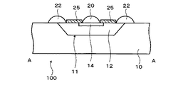
図1は、本発明の第1の実施の形態にかかる機能ブロック12を含む装置100を模式的に示す断面図である。図2は、図1に示す装置100の平面図である。図1は、図2のA−A線における断面を示している。
【0056】
装置100は、基体10と、基体10の凹部11に設けられた機能ブロック12とを含む。
【0057】
基体10は、シリコン、ガラス、プラスチック等の材料からなる。基体10の材質は、機能素子および機能ブロック12の種類や、装置100の用途に応じて適宜選択される。
【0058】
機能ブロック12は、背景技術の欄で前述したFSA法によって、基体10の凹部11に嵌め込まれて形成される。機能ブロック12は、半導体デバイスを含むことができる。なお、図1においては、機能ブロック12が四角錐台状である例を示したが、機能ブロック12の形状はこれに限定されるわけではなく、用途および機能に応じて種々の形状をとることができる。
【0059】
機能ブロック12の表面には、機能素子として光学素子14が形成されている。光学素子14はたとえば、VCSEL(vertical cavity surface emitting laser;面発光型半導体レーザ)、LED(light emitting diode;発光ダイオード)、EL素子(electroluminescent device)等の発光素子、あるいはフォトコンダクタ(photoconductor)や、PD(photo diode)等の受光素子である。
【0060】
光学素子14の上には、機能的形状部であるレンズ形状部20が形成されている。レンズ形状部20は透明であり、かつ凸レンズ形状を有する。すなわち、レンズ形状部20の上面は凸レンズ面を構成する。
【0061】
光学素子14が発光素子の場合、レンズ状形状部20は光学素子14から出射する光を屈折させる機能を有する。一方、光学素子14が受光素子の場合、レンズ状形状部20は光を屈折させ光学素子14の所定の領域へ集光させる機能を有する。
【0062】
レンズ形状部20の材質は、特に限定されるものではないが、たとえば、ポリイミド系樹脂、紫外線硬化型アクリル系樹脂、紫外線硬化型エポキシ系樹脂などの高分子化合物から形成されることが望ましく、ポリイミド系樹脂から形成されているのがより望ましい。
【0063】
機能ブロック12の上には、電極層25が形成されている。電極層25は上部電極であり、コンタクト(図示せず)によって光学素子14と電気的に接続され、さらに、電極層25が外部電極(図示せず)と接続されることにより、光学素子14に電力が供給される。なお、図2においては電極層25の図示を、図1および図2においては下部電極の図示をそれぞれ省略する。
【0064】
また、固定部22は、基体10の表面において機能ブロック12と基体10との境界領域の少なくとも一部を覆うように形成されている。固定部22も機能的形状部として機能する。すなわち、固定部22は、基体10の凹部11に嵌め込まれた機能ブロック12を固定する手段として機能を有する。
【0065】
なお、本実施の形態では、機能素子が光学素子14である場合を示したが、機能素子は光学素子に限定されるわけではなく、たとえば、トランジスタ等を用いることができる。また、機能的形状部も、レンズ形状部20や固定部22に限定されるわけではなく、たとえば、平面導波路やスペーサ等であってもよい。
【0066】
(デバイスの動作)
以下に、機能ブロック12を含む装置100の動作を説明する。
【0067】
光学素子14が発光素子の場合、光学素子14が駆動することにより生じた光が、光学素子14の上面の所定の領域から出射する。レンズ状形状部20は、出射面において、この出射光を屈折させ、その放射角を狭めることができる。また、光学素子14の上面に形成される光の出射口の径を大きくした場合であっても、レンズ状形状部20を用いることにより、出射光の放射角を狭めることができる。
【0068】
一方、光学素子14が受光素子の場合、レンズ状形状部20に入射した光は屈折して光学素子14の所定の領域へ集光する。この集光した光が光学素子14によって電気信号へと変換される。
【0069】
(デバイスの製造プロセス)
次に、図1に示す装置100の製造プロセスについて説明する。図3および図4は、装置100の製造工程の一例を示す図である。
【0070】
(1)光学素子14を含む機能ブロック12の形成、ならびに機能ブロック12の凹部11への嵌め込みは、背景技術の欄で説明したFSA法を用いて行なう。この工程により、光学素子14を含む機能ブロック12が凹部11に嵌め込まれた基体10が得られる。
【0071】
(2)次に、機能ブロック12上面において、光学素子14上、ならびに機能ブロック12と基体10との境界領域に液状物を塗布する。液状物を塗布する方法として、ディスペンサノズル27により液状物を供給する方法について、図3(a),図3(b)を参照しながら説明する。図3(a),図3(b)は、ノズル27により液状物24を光学素子14上に供給する方法を経時的に表した模式図である。
【0072】
レーザ出射部の構成材質となる樹脂またはその樹脂の前駆体の液状物24をノズル27に注入する。ノズル27の先端にこの液状物24の液滴を作った後、図3(a)に示すように、この液滴を機能ブロック12上に接触させる。そして、図3(b)に示すように、光学素子14上でノズル27を離し、光学素子14上に液状物24を移す。ノズル27を用い同様の方法にて、機能ブロック12と基体10との境界領域にも液状物24を形成する。
【0073】
このように、ノズルにより液状物を機能ブロック12上に供給する方法によれば、液状物の粘度、ノズル径およびノズル先端の液滴量などを調整したり、ノズル先端の表面処理などにより、レンズ形状部20の厚さを容易に制御することができる。また、ノズルによる液状物の供給方法は、液状物の粘度による影響を受けにくいため、使用可能な液状物の範囲が広い。さらに、必要なところのみ液状物を確実に供給することができるため、無駄がなく、余計なところに液状物が付着することもない。
【0074】
樹脂の液状物としては、たとえば、紫外線硬化型アクリル系樹脂、紫外線硬化型エポキシ系樹脂などを挙げることができる。前駆体の液状物としては、ポリイミド前駆体の液状物、紫外線硬化型アクリル系樹脂および紫外線硬化型エポキシ系樹脂のモノマーを含む液状物などを挙げることができる。
【0075】
紫外線硬化型樹脂は、紫外線照射のみで硬化することができるため、素子への熱によるダメージや、熱硬化させた場合に生じる半導体層と樹脂との熱膨張差によるレーザ出射部の剥離などの心配がない。
【0076】
紫外線硬化型樹脂は、プレポリマー、オリゴマーおよびモノマーのうち少なくとも1種と光重合開始剤を含んだものからなる。
【0077】
紫外線硬化型アクリル系樹脂の具体例としては、プレポリマーまたはオリゴマーとしては、たとえば、エポキシアクリレート類、ウレタンアクリレート類、ポリエステルアクリレート類、ポリエーテルアクリレート類、スピロアセタール系アクリレート類等のアクリレート類、エポキシメタクリレート類、ウレタンメタクリレート類、ポリエステルメタクリレート類、ポリエーテルメタクリレート類等のメタクリレート類等が利用できる。
【0078】
モノマーとしては、たとえば、2−エチルヘキシルアクリレート、2−エチルヘキシルメタクリレート、2−ヒドロキシエチルアクリレート、2−ヒドロキシエチルメタクリレート、N−ビニル−2−ピロリドン、カルビトールアクリレート、テトラヒドロフルフリルアクリレート、イソボルニルアクリレート、ジシクロペンテニルアクリレート、1,3−ブタンジオールアクリレート等の単官能性モノマー、1,6−ヘキサンジオールジアクリレート、1,6−ヘキサンジオールジメタクリレート、ネオペンチルグリコールアクリレート、ポリエチレングリコールジアクリレート、ペンタエリスリトールジアクリレート等の二官能性モノマー、トリメチロールプロパントリアクリレート、トリメチロールプロパントリメタクリレート、ペンタエリスリトールトリアクリレート、ジペンタエリスリトールヘキサアクリレート等の多官能性モノマーが挙げられる。
【0079】
光重合開始剤としては、たとえば、2,2−ジメトキシ−2−フェニルアセトフェノンなどのアセトフェノン類、α−ヒドロキシイソブチルフェノン、p−イソプロピル−α−ヒドロキシイソブチルフェノンなどのブチルフェノン類、p−tert−ブチルジクロロアセトフェノン、p−tert−ブチルトリクロロアセトフェノン、α,α−ジクロロ−4−フェノキシアセトフェノンなどのハロゲン化アセトフェノン類、ベンゾフェノン、N,N−テトラエチル−4,4−ジアミノベンゾフェノンなどのベンゾフェノン類、ベンジル、ベンジルジメチルケタールなどのベンジル類、ベンゾイン、ベンゾインアルキルエーテルなどのベンゾイン類、1−フェニル−1,2−プロパンジオン−2−(o−エトキシカルボニル)オキシムなどのオキシム類、2−メチルチオキサントン、2−クロロチオキサントンなどのキサントン類、ベンゾインエーテル、イソブチルベンゾインエーテルなどのベンゾインエーテル類、ミヒラーケトン類のラジカル発生化合物を挙げることができる。紫外線硬化型アクリル系樹脂を硬化した後の樹脂は、透明度が高いという利点を有しており、レンズに適している。
【0080】
ポリイミド前駆体としては、ポリアミック酸、ポリアミック酸の長鎖アルキルエステルなどを挙げることができる。ポリイミド前駆体を熱硬化させて得られたポリイミド系樹脂は可視光領域において、80%以上の透過率を有し、屈折率が1.7〜1.9と高いため、大きなレンズ効果が得られる。
【0081】
(3)つづいて、機能ブロック12上の液状物24を硬化させて、光学素子14上にレンズ形状部20を形成するとともに、機能ブロック12と基体10との境界領域に固定部22を形成する。液状物24が前述の紫外線硬化型樹脂の場合には、紫外線を照射することにより、硬化させることができる。
【0082】
また、液状物として、ポリイミド前駆体の液状物を用いた場合には、ポリイミド前駆体の液状物を加熱キュア処理してイミド化反応を起こしポリイミド系樹脂を生成させることにより、硬化させることができる。キュア温度は、前駆体の種類によって異なるが、機能ブロック12を構成する光学素子14等への熱によるダメージ、基体10とポリイミド系樹脂との熱膨張差、および電極層25のアロイングの防止などの観点から、150℃程度が適当である。
【0083】
前述した(2)において、液状物を機能ブロック12上に供給する方法として、ディスペンサノズル27による供給方法を例示したが、図4(a)および図4(b)に示すように、インクジェットヘッド28を用いて、液状物24を機能ブロック12上に射出して供給する方法なども適用することができる。インクジェットヘッド28を用いた方法は、短時間で液状物を機能ブロック12上に供給することができ、生産性が高いという利点がある。液状物をインクジェットにより塗布する際、液状物の液粘度は、重要な要素であるが、希釈溶剤を液状物に添加することにより、適当な液粘度に調整することもできる。
【0084】
紫外線硬化型樹脂の液状物に適用可能な希釈溶剤としては、特に限定されるものではないが、たとえば、プロピレングリコールモノメチルエーテルアセテート、プロピレングリコールモノプロピルエーテル、メトキシメチルプロピオネート、メトキシエチルプロピオネート、エチルセロソルブ、エチルセロソルブアセテート、エチルラクテート、エチルピルビネート、メチルアミルケトン、シクロヘキサノン、キシレン、トルエン、ブチルアセテートなどを挙げることができ、単独で、または、2種以上を混合して使用することができる。
【0085】
ポリイミドの前駆体の液状物に適用可能な希釈溶剤としては、たとえば、N−メチル−2−ピロリドンを挙げることができる。
【0086】
(4)さらに、機能ブロック12上の所定の領域に、一般的なメタライズ法等を用いて、機能ブロック12を駆動させるための電極層25を形成する。なお、本実施の形態においては、レンズ形状部20を形成した後に電極層25を形成する例を示したが、レンズ形状部20を形成する前に電極層25を形成することもできる。以上の工程により、図1に示す機能ブロック12を含む装置100が得られる。
【0087】
以上説明したように、本実施の形態の機能ブロック12を含む装置100では、機能ブロック12が機能素子として光学素子14を含み、かつ機能ブロック12上の所定の領域に、機能的形状部であるレンズ形状部20が形成されている。光学素子14が受光素子の場合、レンズ形状部20は入射する光を集光することができる。また、光学素子14が発光素子の場合、レンズ形状部20は光学素子14から出射する光の放射角を狭めることができる。このように、機能ブロック12を含む装置100において、機能的形状部であるレンズ形状部20が光学素子14上に設けられていることにより、機能素子である光学素子14の機能を高めることができる。
【0088】
また、機能ブロック12と基体10とを固定するための固定部22を、レンズ形状部20と同一工程で形成することができるため、工程数を少なくすることができる。
【0089】
[第2の実施の形態]
(デバイスの構造)
図5は、本発明の第2の実施の形態にかかる機能ブロック12を含む装置200を模式的に示す断面図である。
【0090】
本実施の形態の機能ブロック12を含む装置200は、機能ブロック12の表面において基体10と機能ブロック12との境界領域全面を覆うように保護層18が形成されている点、ならびに光学素子14の表面は液状樹脂に対して親和性を有する一方、電極層125の表面は液状樹脂をはじく性質を有するように処理されており、その結果、図5に示すように、光学素子14上に設けられた電極層125の開口部に、セルフアラインでレンズ状の樹脂(レンズ形状部120)が形成されている点で、第1の実施の形態にかかる装置100と異なる。この他の部分については第1の実施の形態にかかる装置100と近似する構造を有する。近似する構造を有する部分については詳細な説明は省略する。なお、機能ブロック12を含む装置200において、第1の実施の形態にかかる装置100と同一の構成要素については、同一番号を付すものとする。
【0091】
レンズ形状部120は、第1の実施の形態にかかるレンズ形状部20と同様の作用および効果を有する。すなわち、レンズ形状部120が機能的形状部であり、光学素子14が機能素子である。したがって、光学素子14が受光素子の場合には、レンズ形状部120は光を屈折させて光学素子14の所定の領域へ集光させる機能を有し、光学素子14が発光素子の場合にはレンズ形状部120は出射する光を屈折させ、放射角を小さくする機能を有する。
【0092】
(デバイスの動作)
第2の形態にかかる機能ブロックを含む装置200の動作は、第1の実施の形態にかかる装置100の動作と同様である。よって、その説明を省略する。
【0093】
(デバイスの製造プロセス)
次に、図5に示す機能ブロック12を含む装置200の製造プロセスについて説明する。図6および図7は、装置200の製造工程の一例を示す図である。
【0094】
(1)まず、第1の実施の形態にかかる装置100と同様に、背景技術の欄で説明したFSA法を用いて、光学素子14を含む機能ブロック12が凹部11に嵌め込まれた基体10を形成する。
【0095】
ここで、機能ブロック12の表面を、液状物(後述する)に対して親和性を有する材質から形成する。すなわち、機能ブロック12の表面を、前記液状物をはじかない材質から形成する。これにより、後述する工程において、機能ブロック12上に前記液状物を移す際に、機能ブロック12上で前記液状物が安定して存在することができる。
【0096】
(2)つづいて、図6に示すように、機能ブロック12上に電極層125を形成する。この電極層125は、機能ブロック12を駆動させるための電力を供給するために設けられる。図5に示す装置200においては、電極層125の一部が光学素子14上に設置されている。
【0097】
(3)次に、電極層125上に撥液膜110を形成する。撥液膜110は、後述する液状物をはじく性質を有している。
【0098】
ここで、電極層125を構成する金属層の表面が金層115である場合には、撥液膜110としては、たとえば、以下のようにして得られた単分子膜からなる。
【0099】
機能基を末端に有するチオールを1〜10mMのエタノール水溶液に溶解させる。その溶液に電極層125を浸漬すると、電極層125上にのみ、機能基を末端に有するチオールの単分子膜(以下「チオール単分子膜」という)が形成される。
【0100】
ここで、機能基を末端に有するチオールとしては、たとえば、CF3(CF2)n(CH2)mSH(mは、5〜60の整数、nは、1〜20の整数を示す)で表されるフッ素系の機能基を末端に有するチオールなどを挙げることができる。
【0101】
以下に、図6および図7を参照して、電極層125上に、チオール単分子膜116が形成される理由を説明する。
【0102】
図7は、チオール単分子膜116を形成した直後の光学素子14および電極層125の表面の一部分を模式的に示した拡大図であり、図6に示す領域A100部分の拡大図である。
【0103】
チオールは、チオールのメルカプト基の硫黄原子と金原子とが共有結合的に化学結合することにより、金に化学吸着する性質を有する。この性質のため、金層115からなる電極層125を、機能基114を有するチオールを含む溶液に浸漬すると、図7に示すように、機能基114を末端に有するチオール112は、メルカプト基113を電極層125に向けた配向をとって電極層125の表面上に化学吸着される。一方、光学素子14を含む機能ブロック12の表面には、機能基114を末端に有するチオール112は化学吸着しない。また、末端に存在している機能基114は、チオール単分子膜116の表面に現れる。その結果、電極層125上に、チオール単分子膜116を形成することができる。
【0104】
このチオール単分子膜116は、以下のような理由で、撥液膜110として作用する。
【0105】
このチオール単分子膜116の表面には、図7に示すように、後述する液状物をはじく性質が付与された機能基114が現れている。このため、チオール単分子膜116は、後述する液状物をはじく性質を有し、撥液膜110として作用することができる。
【0106】
このように化学吸着を利用して撥液膜110を形成する利点は、電極層125上に、選択的に、かつ、簡便に撥液膜110を形成することができる点にある。
【0107】
上記実施の形態において、撥液膜110は、機能基114を有するチオールからなる単分子膜について述べたが、この化合物に限らず、電極層125に吸着し、かつ、上記の液状物をはじく性質を有する単分子膜であれば、本発明の撥液膜110として適用することができる。また、撥液膜110は、単分子膜に限られるものではなく、液状物をはじく性質を有する膜であれば、特に限定されない。また、撥液膜110は、必要に応じて、適宜、剥離することができる。
【0108】
また、上記の製造プロセスでは、電極層125を構成する金属層の表面が金層115である場合について述べたが、撥液膜111と密着するものであれば、特に限定されるものではない。
【0109】
(4)つづいて、光学素子14を含む機能ブロック12上に液状物(図示せず)を供給する。液状物を供給する方法は、第1の実施の形態にかかる装置100の製造工程で用いた場合と同様に、ディスペンサノズルによる方法、またはインクジェットによる方法を用いることができる。あるいは、スピンコート法、ディッピング法、スプレーコート法、ロールコート法、バーコート法などを利用することができる。
【0110】
光学素子14を含む機能ブロック12は、その表面が液状物をはじかない材質からなる。そのため、光学素子14を含む機能ブロック12上に液状物を供給した場合、露出した機能ブロック12上に移された液状物が安定して存在することができる。また、電極層125上にはみだした液状物は、電極層125上に形成された撥液膜110によりはじかれる。はじかれた液状物は、機能ブロック12の露出面上の液状物に吸収される。その結果、液状物は、機能ブロック12の露出面上に残る。残った液状物は、表面張力により、マイクロレンズの原形となるレンズ形状部120および保護層18の形状を形作る。
【0111】
(5)さらに、機能ブロック12上の液状物を硬化させることにより、光学素子14上にレンズ形状部120を形成するとともに、機能ブロック12と基体10との境界領域を全面的に覆う保護層18を形成する。以上の工程により、図5に示す装置200が得られる。
【0112】
本実施の形態の機能ブロックを含む装置200は、第1の実施の形態にかかる装置100と同様の作用および効果を有する。
【0113】
また、本実施の形態の装置200の製造方法によれば、前記液状物を機能デバイス12に供給してやり、前記液状物を硬化することのみで、マイクロレンズとして機能するレンズ形状部120をセルフアラインで形成することができる。その結果、光軸合わせが不要で光軸ずれのないレンズ形状部120をきわめて簡単な工程で形成することができる。くわえて、レンズ形状部120の形成と同時にコンタクトホール16をセルフアラインで形成することができるため、工程数を少なくすることができる。
【0114】
さらに、レンズ形状部120を形成する際に、電極層125に撥液膜110を形成してから液状物を供給することにより、レンズ形状部120の大きさおよび形状を容易に制御することができる。
【0115】
[第3の実施の形態]
(デバイスの構造)
図8は、本発明の第3の実施の形態にかかる機能ブロック12を含む装置300を模式的に示す断面図である。
【0116】
本実施の形態の機能ブロック12を含む装置300は、保護層118が基体10と機能ブロック12との境界領域全面を覆うように形成されている点で、第2の実施の形態にかかる装置200と近似する構造を有する。このため、近似する構造を有する部分については詳細な説明を省略する。一方、本実施の形態にかかる装置300には、コンタクトホール16が設けられている点で、第1および第2の実施の形態にかかる装置100,200と異なる。なお、装置300において、第1および第2の実施の形態にかかる装置100,200とほぼ同一の構成要素については、同一番号を付すものとする。
【0117】
装置300には、レンズ形状部220を含む保護層119が設けられている。レンズ形状部220は、第1の実施の形態にかかるレンズ形状部20と同様の作用および効果を有する。すなわち、レンズ形状部220は機能的形状部であり、光学素子14が機能素子である。したがって、光学素子14が受光素子の場合には、レンズ形状部220は光を屈折させて光学素子14の所定の領域へ集光させる機能を有し、光学素子14が発光素子の場合にはレンズ形状部220は出射する光を屈折させ、放射角を小さくする機能を有する。
【0118】
また、コンタクトホール16は、電極層225上に形成され、電極層225と外部電極(図示せず)とを接続するコンタクトの一部を構成する。
【0119】
(デバイスの動作)
第3の形態にかかる機能ブロック12を含む装置300の動作は、第1の実施の形態にかかる装置100の動作と同様である。よって、その説明を省略する。
【0120】
(デバイスの製造プロセス)
次に、図8に示す装置300の製造プロセスについて説明する。図9〜図11は、装置300の製造工程の一例を示す図である。
【0121】
(1)まず、第1の実施の形態にかかる装置100と同様に、背景技術の欄で説明したFSA法を用いて、光学素子14を含む機能ブロック12が凹部11に嵌め込まれた基体10を形成する。
【0122】
(2)つづいて、図9に示すように、機能ブロック12上に電極層225を形成する。ここまでの工程は、第2の実施の形態にかかる装置200とほぼ同様である。
【0123】
(3)次に、機能ブロック12上にレンズ形状部220および保護層118,119を形成するプロセスについて説明する。図10および図11は、保護層118,119の製造工程を示す断面図である。
【0124】
まず、図10に示すスタンパ29を形成する。スタンパ29は紫外線に対して透明な材質から形成される。また、スタンパ29は鋳型面29aを有する。鋳型面29aは凹部23と凸部26とを含み、最終的に製造される装置300のレンズ形状部220とコンタクトホール16の形状の反転形状を有する。すなわち、凹部23は最終的に製造されるレンズ形状部220の反転形状部となり、凸部26は最終的に製造されるコンタクトホール16の反転形状部となる。
【0125】
鋳型面29aには表面処理を施すことが望ましい。この表面処理は、後述する保護層118,119とスタンパ29との密着性が、その保護層118,119と機能ブロック12との密着性よりも低くなるようにするもの、すなわち、後述する保護層118,119とスタンパ29との剥離をする工程において、その剥離を容易にするために行なう。この表面処理としては、たとえばCF4ガスプラズマによるフッ素処理などを挙げることができる。このようにして、スタンパ29を作製する。
【0126】
また、スタンパ29は、まず母型を形成し、この母型の形状を反転転写させて作製される。この母型は、最終的に製造される装置300のレンズ形状部220とコンタクトホール16の形状を有する。あるいは、スタンパ29を基体から直接作製してもよい。すなわち、ウエットエッチング法を用いて、基体に凹部23および凸部26を形成することにより、スタンパ29を作製することもできる。この場合、スタンパ29を形成するための基体の材質としては、樹脂の他に、金属、半導体基板(たとえばシリコン)、石英、ガラスなどを用いることができる。
【0127】
(4)次に、このスタンパ29の凹部23が光学素子14上に位置するように、スタンパ29と基体10とをアライメントをする。アライメント方法としては、たとえば、以下の方法を挙げることができる。
1)スタンパ29と基体10とを別々に位置決めし、機械的精度で張り合わせる方法。
2)スタンパ29が透明な場合において、機能ブロック12が形成されている側の基体10の表面に、アライメントの際の照準となるアライメントマークを付して、そのアライメントマークを利用してアライメントを行う方法。
3)スタンパ29が透明でない場合には、基体10上にスタンパ29が設置される際に基体10においてスタンパ29と重なる面と垂直方向に、スタンパ29を貫通する孔を設け、その孔を介して、上述のアライメントマークを利用してアライメントを行う方法。
【0128】
(5)スタンパ29と基体10とをアライメントした後、樹脂の液状物118aをスタンパ29と基体10との間に導入し、図10に示すように、基体10の面上に載せる。また、樹脂の液状物50を基体10の面上に載せた後、スタンパ29と基体10とをアライメントしてもよい。
【0129】
樹脂の液状物118aとしては、エネルギーを付与することにより硬化するものが好ましい。樹脂が液状物であることで、スタンパ29の凹部23へ樹脂を充填することが容易となる。樹脂の液状物118aとしては、たとえば、第1の実施の形態の欄で例示したように、紫外線硬化型のアクリル系樹脂、紫外線硬化型のエポキシ系樹脂あるいは熱硬化型のポリイミド系樹脂の前駆体などを挙げることができる。特に、紫外線硬化型の樹脂は、紫外線照射のみで硬化することができるので、手軽に使用することができる。また、紫外線硬化型の樹脂の硬化の際には熱処理を加えないので、スタンパ29と、光学素子14を含む機能ブロック12との間の熱膨張差に起因するトラブルを心配する必要がない。
【0130】
樹脂の液状物118aの基体10上への導入方法は、特に限定されるものではなく、たとえば、第2の実施の形態の欄で例示した方法、スピンコート法、ディッピング法、スプレーコート法、ロールコート法、バーコート法などを利用することができる。
【0131】
(6)次いで、スタンパ29と基体10とを、樹脂を介して密着させる。このように、スタンパ29と基体10とを密着させることにより、樹脂の液状物118aは、図11に示すように、所定領域まで塗り拡げられ、スタンパ29と基体10との間に樹脂の液状物118aからなる層が形成される。なお、必要に応じて、スタンパ29と基体10とを貼り合わせる際に、スタンパ29および基体10の少なくともいずれか一方を介して加圧してもよい。また、液状物118aの内部に気泡が混入することを防ぐため、10Pa程度の真空下で、スタンパ29と基体10とを密着させてもよい。
【0132】
(7)続いて、樹脂の液状物118aを硬化する。硬化方法は、樹脂の液状物118aの種類に応じて適宜の方法が選択され、第1の実施の形態の欄で説明した方法を用いることができる。紫外線硬化型の樹脂を用いた場合には、紫外線をスタンパ29側から樹脂の液状物118aに照射することにより、硬化することができる。
【0133】
以上の工程によって、基体10上に、スタンパ29の鋳型面29aに対応した形状が転写され、保護層118、ならびにレンズ形状部220を含む保護層119が形成される。すなわち、図8に示すように、スタンパ29の凹部23に対応する部分にレンズ形状部220が形成され、凸部26に対応する部分にコンタクトホール16が形成される。
【0134】
(8)つづいて、スタンパ29を保護層118,119および基体10から剥離する。この際、スタンパ29の鋳型面29aには、前述の工程により、スタンパ29が保護層118,119から離れ易くするための表面処理が施されていると、スタンパ29を保護層118,119および基体10から容易に剥離することができる。
【0135】
スタンパ29を剥離した後、コンタクトホール16の底部に樹脂が残存する場合がある。樹脂が残存してしまうと、コンタクトホール16の底部に金属層を設け、この金属層と電極層225とをコンタクトホール16を介して電気的な接触を取りたい場合に、電極層225とその金属層との電気的な接触が十分に図れなくなる。また、コンタクトホール16の底部に樹脂が残存した状態で、たとえば、電極層225に直接にワイヤボンディングを行うと、ワイヤと電極層225とを接続できなくなる問題が生じる場合がある。また、ワイヤを電極層225に接続できたとしても、ワイヤと電極層225との電気的な接触が十分に図れなくなるなどの問題が生じる。そのため、コンタクトホール16の底部に樹脂が残存した場合には、その残存した樹脂を除去するために、たとえば、以下に示す2つの工程のうち、いずれかの工程を行うことが望ましい。
【0136】
第1に、アッシング、すなわち、樹脂を気相中で除去する方法を用いてコンタクトホール16の底部に残存した樹脂を除去する。アッシングの具体例としては、オゾンアッシング、プラズマアッシングなどを挙げることができる。オゾンアッシングは、高濃度のオゾンの雰囲気下で、オゾンとレジストを化学反応させて、樹脂を除去する方法である。プラズマアッシングは、反応性ガス、たとえば、酸素ガスのプラズマを発生させて、そのプラズマを利用して樹脂を除去する方法である。このようなアッシングによる方法によれば、全てのコンタクトホール16について残存した樹脂を除去することができるので、処理時間を要しないという利点がある。
【0137】
第2に、コンタクトホール16の底部をエキシマレーザでアブレーションする。すなわち、細かく絞ったエキシマレーザビームをコンタクトホール16の底部に照準を合わせて照射し、コンタクトホール16の底部の樹脂を焼き飛ばす。エキシマレーザによれば、確実にコンタクトホール16の底部のみ処理を行うことができるので、レンズ形状部220の破損を心配する必要がないという利点がある。
【0138】
以上の工程により、図1に示すように、本実施の形態にかかる装置300が得られる。
【0139】
本実施の形態にかかる装置300は、第1の実施の形態にかかる装置300とほぼ同様の作用および効果を有する。さらに、上述した製造方法は、スタンパ29を利用して一体的にレンズ形状部220とコンタクトホール16を形成することができるため、たとえばフォトリソグラフィ法を用いてレンズ形状部220とコンタクトホール16を形成する場合と比較して、簡単であり、製造に要する時間を大幅に短縮することができる。また、スタンパ29は、一度作成すれば、再度繰り返して使用することができるため、製造コストを削減することができ、経済的である。
【0140】
上記実施の形態において、スタンパ29は、紫外線に対して透明であるものであったが、これに限定されず、紫外線に対して透明でない材質、たとえば金属からなってもよい。スタンパ29が金属からなる場合には、電鋳を用いてスタンパ29を製造することができる。電鋳を用いたスタンパ29の製造は、スタンパ29を簡便に製造することができるという利点を有する。
【0141】
スタンパ29が金属や半導体のように紫外線を透過することが困難な材質からなる場合には、樹脂の液状物は、紫外線硬化型の樹脂を適用することはできないが、熱硬化性の樹脂、たとえば、上述した熱硬化型のポリイミド系樹脂の前駆体を使用すれば、上記実施の形態と同様の作用効果を得られる。
【0142】
また、上記の実施の形態における装置の駆動方法は一例であり、本発明の趣旨を逸脱しない限り、種々の変更が可能である。また、上記の実施の形態では、1の機能ブロックに1の光学素子(機能素子)を含む装置を示しているが、1の機能ブロックに機能素子が複数個あっても本発明の形態は損なわれない。
【0143】
以下、本発明の光伝送装置の2つの実施形態について説明する。
図12は、本発明の光伝送装置の第1実施形態である積層ICチップ間の光インターコネクション装置の概略構成図であり、ここでは、CPUやDRAM等のICチップ(LSI)1001a〜1001cを三層積層している。この実施形態では、図示する最下層のICチップ1cの発光素子1002aの光を中層及び最上層のICチップ1001b、1001aの受光素子1003aで受光し、最上層のICチップ1001aの発光素子1002bの光を中層及び最下層のICチップ1001b、1001cの受光素子3bで受光するように構成されている。そのため、一方の発光素子1002aは他方の発光素子1002bと発光波長が異なり、また一方の受光素子1003bは他方の受光素子1003bと感受する受光波長帯域が異なる。なお、この実施形態では、各ICチップ1001a〜1001cの基板(基体)1004a〜1004c及び機能ブロック1007a〜1008bをSiで作製した。そのため、各発光素子の光として1.0μm以上、好ましくは1.1μm以上の波長を選んでいる。Siは1.0μmの波長に対して約100cm-1と吸収係数が大きく、相応の損失がある。一方、波長が1.1μm以上では、吸収係数は10cm-1以下と小さい。そこで、本実施形態では、各発光素子の光の波長を1.0μm以上、好ましくは1.1μm以上とした。この波長の光ならば、Siを容易に透過することができるため、対向する受発光素子間の光信号の伝達が良好にできる。勿論、後述する接着層1021も、この波長帯域の光に対して透明である。
【0144】
前記各ICチップ1001a〜1001cの各基板1004a〜1004cのうち、前記各発光素子1002a、1002b及び受光素子1003a、1003bを実装すべき部位には、凹部1005b(1005a)、1006a(1006b)が形成されている。各凹部1005b、1006aは、上方形面より下方形面が小さく、且つ側面が台形状の凹部である。これらの凹部1005b、1006aは、Siを異方性エッチングすることによって、特に側面の傾きなど、極めて精度よく、形成することができる。なお、少なくとも同じ基板1004a上の発光素子用凹部1005bと受光素子用凹部1006aとは、大きさ等の形態が異なる。また、本実施形態では、図12に示すように、その他の凹部、例えば中層のICチップ1001bの基板1004bの受光素子用凹部1006a、1006b同士も、最下層のICチップ1001cの基板1004cの受光素子用凹部1006bと発光素子用凹部1005aとも大きさ等の形態が異なっている。つまり、例えば1006aや1006bのように、同じ符号を付している凹部同士は大きさ等の形態が同じであるが、符号の異なる凹部同士は、互いに大きさ等の形態が異なる。換言すれば、同じ機能の素子が必要な部位の凹部は形態が同じであるが、異なる機能の素子用の凹部は形態が異なるのである。
【0145】
次に、本発明の光伝送装置を波長多重型光インターコネクション装置に適用した第2実施形態を示す。波長多重型光インターコネクション装置は、例えば図13のように構成される。この例は、例えば特開平11−289317号公報に記載されるものと同等であり、波長の異なる複数の発光素子1002が実装されている発光素子アレイ1111と、光導波路となる光ファイバ1110と、前記発光素子1002の夫々の波長の光を抽出するフィルタ素子1122が実装されているフィルタアレイ1112と、このフィルタアレイ1112で抽出された各波長の光を受光する受光素子1003が実装されている受光素子アレイ1113とで構成される。なお、図では、理解を容易にするために、各構成要素を分離しているが、実質的に各構成要素は、光学的に直接接合されている。
【図面の簡単な説明】
【図1】 本発明の第1の実施の形態にかかる機能ブロックを含む装置を模式的に示す断面図である。
【図2】 図1に示す装置の平面図である。
【図3】 図3(a),図3(b)ともに、ノズルを用いて液状物を柱状部の上面に供給する方法を経時的に表した模式図である。
【図4】 図4(a),図4(b)ともに、インクジェットヘッドを用いて液状物を柱状部の上面に供給する方法を経時的に表した模式図である。
【図5】 本発明の第2の実施の形態にかかる機能ブロックを含む装置を模式的に示す断面図である。
【図6】 図5に示す装置の製造工程の一例を示す断面図である。
【図7】 図6に示す領域A100の拡大図である。
【図8】 本発明の第3の実施の形態にかかる機能ブロックを含む装置を模式的に示す断面図である。
【図9】 図8に示す装置の製造工程の一例を示す断面図である。
【図10】 図8に示す装置の製造工程の一例を示す断面図である。
【図11】 図8に示す装置の製造工程の一例を示す断面図である。
【図12】 本発明の光伝送装置の第1実施形態を示す概略構成図である。
【図13】 本発明の光伝送装置の第2実施形態を示す概略構成図である。
【符号の説明】
10 基体
11 凹部
12 機能ブロック
14 光学素子
16 コンタクトホール
18,118,119 保護層
20,120,220 レンズ形状部
22 固定部
23 凹部
24 液状物
25,125,225 電極層
26 凸部
27 ノズル
28 インクジェットヘッド
29 スタンパ
100,200,300 装置
110 撥液膜
112 機能基を末端に有するチオール
113 メルカプト基
114 機能基
115 金層
116 チオール単分子膜
118a 液状物[0001]
The present inventionOptical deviceAnd manufacturing method thereofAnd optical transmission equipmentAbout.
[0002]
[Background]
In recent years, a mounting method using an FSA (Fluidic Self-Assembly) method has been developed as one of electronic device mounting methods. In the FSA method, an electronic device having a size of 10 to several hundred microns and a predetermined shape (hereinafter referred to as “functional device”) is dispersed in a liquid, and a hole or In this technique, the liquid is poured onto the surface of the base including the fitting portion, and the functional device is fitted into the hole or the fitting portion to mount the functional device on the base. Regarding the FSA method, for example, Information Display magazine (S. Drobac. INFORMATION DISPLAY VOL. 11 (1999),
[0003]
Next, an example of a semiconductor device mounting process using the FSA method will be briefly described.
[0004]
(1) First, a wafer made of single crystal silicon and including hundreds to millions of electronic devices is divided into thousands to millions of functional blocks by etching. The functional blocks obtained by the division have a predetermined three-dimensional shape, and each has a predetermined function. The electronic device may have a simple structure such as a transistor, or may have a complicated structure such as an IC.
[0005]
(2) Apart from the above-described functional blocks, a base body into which these functional blocks are fitted is formed. Holes for fitting the functional blocks are formed in the base body by using stamping, etching, laser, or the like. This hole is formed to match the size and shape of the functional block.
[0006]
(3) Next, the functional block formed by the above-mentioned process is dispersed in a liquid, and this dispersion liquid is allowed to flow on the surface of the substrate formed by the process of (2). By this step, the functional block passes through the surface of the base and falls into a hole provided in the base and is fitted in a self-aligning manner. The functional block that has not been fitted into the hole is recovered from the dispersion liquid, cleaned, and then dispersed again in the same cleaned liquid, which is then flowed to another new substrate surface. While the above steps are repeated, the functional block and the dispersion continue to be reused.
[0007]
(4) The functional block fitted in the hole formed in the base is electrically wired by a general metallization method or the like, and functions as a part of the final electric circuit. Through the above steps, the functional block is mounted on the semiconductor device.
[0008]
According to this FSA method, since a large number of functional blocks can be mounted on the substrate at one time, the price of a device such as a display can be reduced, and the production speed can be improved. In addition, since it is possible to mount using only non-defective products that can be driven by inspection in advance as function blocks, the reliability of the apparatus can be improved.
[0009]
In addition, various materials such as glass, plastic, and silicon can be used for the base for fitting the functional blocks, and the degree of freedom in selecting the material used for the base is high. Similarly, the material used for the functional block can be selected according to the function required for the functional block, such as silicon, germanium-silicon, gallium-arsenic, indium-phosphorus, or the like. As described above, the FSA method is expected to have excellent functions and effects as one of the mounting methods of electronic devices.
[0010]
[Problems to be solved by the invention]
By applying a device including a functional block manufactured by using the FSA method to an optical device, for example, development of a highly reliable and low-cost semiconductor device is required. The objective of this invention is providing the apparatus containing a functional block, and its manufacturing method.
[0011]
[Means for Solving the Problems]
In the optical device of the present invention, a functional block having an optical element made of a light emitting element or a light receiving element is fitted in a concave portion of a base, and a convex lens-shaped lens shape portion made of a resin material is formed on the optical element. It is made of the same resin material as the resin material constituting the lens-shaped portion, and the functional block and the substrate are formed on the surface of the substrate on the side where the concave portion is formed.At least part of the boundary areaA fixing portion for fixing the functional block to the base is formed by covering the substrate, and an electrode layer for supplying electric power to the optical element is formed on the functional block.
In the optical device of the present invention, a functional block having an optical element made of a light emitting element or a light receiving element is fitted in a concave portion of a base, and a convex lens-shaped lens shape portion made of a resin material is formed on the optical element. It is made of the same resin material as the resin material constituting the lens-shaped part, and the functional block and the base are formed on the surface of the base on the side where the concave portion is formed.Protective layer covering the entire boundary areaAnd an electrode layer for supplying electric power to the optical element is formed on the functional block.
In the optical device of the present invention, a functional block having an optical element made of a light emitting element or a light receiving element is fitted in a concave portion of a base, and a convex lens-shaped lens shape portion made of a resin material is formed on the optical element. The lens is formed of the same resin material as the resin material constituting the lens-shaped portion, and the functional block and the substrate are formed on the surface of the base on which the concave portion is formed.A protective layer covering the entire boundary region, and a protective layer including the lens shape portionAnd an electrode layer for supplying power to the optical element is formed on the functional block,A contact hole formed by opening a protective layer covering the entire boundary region and a protective layer including the lens-shaped portion is formed on the electrode layer.It is formed.
The method for manufacturing an optical device of the present invention includes a step of fitting a functional block having an optical element made of a light emitting element or a light receiving element into a recess of a base, the optical element, and a boundary between the functional block and the base A step of applying a liquid material comprising a resin or a resin precursor, which will later become a lens shape portion and a fixing portion, and a step of forming the lens shape portion and the fixing portion by curing the liquid material. And forming an electrode layer in a predetermined region on the functional block.
The optical device manufacturing method of the present invention has a functional block formed of a material having an optical element composed of a light-emitting element or a light-receiving element in a recess of a substrate and having a surface having affinity for a liquid material to be used later. , A step of forming an electrode layer in a predetermined region excluding a part on the optical element on the functional block, and a liquid repellency with respect to a liquid material to be used later on the electrode layer A step of forming a liquid repellent film, a step of applying a liquid material made of a resin or a resin precursor, which will later become a lens shape portion and a protective layer, on the functional block including the optical element, and the liquid material Forming the lens-shaped portion and the protective layer by curing.
In the step of forming the liquid repellent film, the liquid repellent film can be selectively formed on the electrode layer using chemical adsorption.
Further, in the step of applying the liquid material, after forming a droplet of the liquid material at the tip of a dispenser nozzle, the droplet is brought into contact with the optical element, and the droplet is removed by releasing the dispenser nozzle. It can be transferred onto the optical element.
Alternatively, in the step of applying the liquid material, the liquid material can be ejected onto the optical element using an inkjet head.
The method for manufacturing an optical device according to the present invention includes a step of fitting a functional block having an optical element made of a light emitting element or a light receiving element into a recess of a base, and a step of forming an electrode layer in a predetermined region on the functional block When,A stamper having a concave portion that is a shape obtained by reversing the shape of a lens shape portion that is formed later and a convex portion that is a shape obtained by reversing the shape of a contact hole that is formed later is used.A step of aligning the stamper and the base so as to be positioned on the optical element, and a liquid material comprising a resin or a resin precursor that will later become a lens-shaped portion and a protective layer is disposed between the stamper and the base. A step of bringing the stamper and the substrate into close contact with each other via the liquid material, and curing the liquid material.The contact hole formed by opening a protective layer covering the entire boundary region, a protective layer including the lens-shaped portion, a protective layer covering the entire boundary region, and a protective layer including the lens-shaped portion.And a step of forming.
An optical transmission device according to the present invention includes a light emitting section including the functional block including the optical block including the optical element including the light emitting element, and a functional block including the optical block including the optical element including the light receiving element. And a light receiving portion made of an optical device.
[0012]
An apparatus including a functional block according to the present invention is an apparatus in which a functional block is disposed in a recess provided in a base. The functional block includes at least a part of a functional element, and is provided in a predetermined region on the functional block. A functional shape is formed.
Here, the functional element refers to an element that can function as an electronic device. Moreover, a functional shape part means the member which has a shape essential in order to exhibit a predetermined function.
[0013]
According to this configuration, the predetermined function can be exhibited by forming the functional shape portion in the predetermined region on the functional block. The above points will be described in detail in the section of the embodiment of the present invention.
[0014]
Preferred embodiments of the device including the functional block include (1) to (4).
[0015]
(1) The functional block may include a semiconductor device.
[0016]
(2) An optical element can be used as the functional element.
[0017]
In this case, the functional shape portion may be formed on the optical element and include a lens shape portion. Here, the optical element is preferably at least one of a light receiving element and a light emitting element. According to this configuration, the function of the optical element can be enhanced. Details will be described in the section of the embodiment of the present invention.
[0018]
(3) An electrode can be formed in a predetermined region on the functional block.
[0019]
(4) Furthermore, a protective layer can be formed on the functional block.
[0020]
In this case, the protective layer can be formed so as to cover at least a part of the boundary region between the functional block and the substrate on the surface of the substrate.
[0021]
Furthermore, in this case, a contact hole can be formed in the protective layer.
[0022]
(Second device)
In addition, the apparatus including the functional block according to the present invention is an apparatus in which the functional block is disposed in the recess provided in the base.
A fixing means for the functional block is provided on at least a part of a boundary region between the functional block and the base on the surface of the base.
[0023]
According to this configuration, the fixing means can be provided at a minimum necessary position for fixing the functional block. Therefore, when a member is provided on the functional block, the degree of design freedom can be increased. .
[0024]
In this case, the fixing means is a functional shape portion. In this case, the functional block may include a semiconductor device.
[0025]
(First manufacturing method)
A method of manufacturing a device including a functional block according to the present invention is a manufacturing method including a step of providing a recess in a base and fitting a functional block including a functional element at least in part into the recess in a self-aligning manner, Step (a) and step (b) are included.
[0026]
(A) applying a liquid material to a predetermined region on the functional block; and
(B) A step of curing the liquid material to form a functional shape portion.
[0027]
According to this manufacturing method, the functional shape portion can be formed by self-alignment only by supplying the liquid material to the functional device and curing the liquid material. As a result, the functional shape portion can be formed by a very simple process without being displaced.
[0028]
(Second manufacturing method)
A method of manufacturing a device including a functional block according to the present invention is a manufacturing method including a step of providing a recess in a base and fitting a functional block including a functional element at least in part into the recess in a self-aligning manner, Step (a) and step (b) are included.
[0029]
(A) applying a liquid material to a predetermined region on the functional block; and
(B) forming the functional shape portion using a stamper having a reverse shape portion of the functional shape portion,
In a state where the functional block and the stamper are aligned, the liquid material is cured to form the functional shape portion so that the inverted shape portion is positioned on a region where the functional shape portion is formed. Process.
[0030]
According to this manufacturing method, it is possible to easily form the functional shape portion with little positional deviation.
[0031]
Further, in the step (b), the stamper further has an inverted shape portion of a contact hole, and the functional shape portion is formed using the stamper and a contact hole is formed on the electrode. can do. According to this manufacturing method, since the functional shape portion and the contact hole can be integrally formed using the stamper, for example, the functional shape portion and the contact hole are formed using a photolithography method. Compared with the case where it forms, the said functional shape part etc. can be formed easily and the time which manufacture requires can be reduced significantly.
[0032]
Preferred embodiments of the first and second production methods described above include (1) to (6).
[0033]
(1) The functional block may include a semiconductor device.
[0034]
(2) An optical element can be used as the functional element.
[0035]
In this case, the step of forming the functional shape portion on the optical element,
A step of forming the functional shape portion so as to include the lens shape portion can be used.
[0036]
(3) Furthermore, the following process (c) can be included.
[0037]
(C) forming an electrode for driving the functional block in a predetermined region on the functional block;
[0038]
(4) Furthermore, the following process (d) can be included.
[0039]
(D) A step of further forming a protective layer on the functional block.
[0040]
In this case, in the step (d), the protective layer can be formed so as to cover at least a part of the boundary region between the functional block and the substrate.
[0041]
(5) The liquid material is preferably a liquid material containing a resin or a resin precursor.
[0042]
(6) In the step (a), as a method of applying a liquid material to a predetermined region on the functional block, for example, a droplet of the liquid material is formed at the tip of a dispenser nozzle, and the liquid droplet is applied to the functional block. It is possible to use a method in which the liquid material is brought into contact with a predetermined region and the liquid material is disposed in the predetermined region. Alternatively, a method can be used in which the liquid material is ejected to a predetermined region of the functional block using an ink head jet, and the liquid material is disposed in the predetermined region.
[0043]
(Third production method)
The first manufacturing method described above can further include the following step (e).
[0044]
(E) A step of forming a liquid repellent film having a property of repelling the liquid material in a region other than the region for forming the functional shape portion before applying the liquid material.
[0045]
In this case, it is preferable that the step (b) included in the first manufacturing method is a step of arranging a liquid material repelled by the liquid repellent film in a region for forming the functional shape portion. . This step will be described in detail in the section of the embodiment of the present invention.
[0046]
In this case, the liquid repellent film is preferably a monomolecular film made of a compound adsorbed on the electrode.
[0047]
Further, in this case, the electrode is preferably formed of a material containing gold, and the monomolecular film is preferably made of a thiol containing an atomic group having a property of repelling the liquid material at one end.
[0048]
(Fourth manufacturing method)
A method of manufacturing a device including a functional block according to the present invention is a manufacturing method including a step of providing a recess in a base and fitting a functional block including a functional element at least in part into the recess in a self-aligning manner, Step (a) and step (b) are included.
[0049]
(A) applying a liquid material to at least a part of a boundary region between the functional block and the substrate on the substrate surface; and
(B) A step of curing the liquid material to form fixing means for the functional block.
[0050]
According to this configuration, since the fixing means can be provided at a minimum necessary position for fixing the functional block, waste of material can be reduced.
[0051]
In this case, it is desirable that the fixing means is a functional shape portion. The functional block may include a semiconductor device.
[0052]
An optical transmission device of the present invention includes a device including the functional block of the present invention in which the functional block including a light emitting element is disposed, and a device including the functional block of the present invention in which the functional block including a light receiving element is disposed. The light emitting element and the light receiving element are stacked so as to face each other.
[0053]
Further, the optical transmission device of the present invention is a light emitting unit comprising the device including the functional block of the present invention in which the functional block including the light emitting element is disposed, and the present invention in which the functional block including the light receiving element is disposed. And a light receiving unit comprising a device including the functional block.
[0054]
DETAILED DESCRIPTION OF THE INVENTION
Hereinafter, preferred embodiments of the present invention will be described with reference to the drawings.
[0055]
[First Embodiment]
(Device structure)
FIG. 1 is a cross-sectional view schematically showing an
[0056]
The
[0057]
The
[0058]
The
[0059]
On the surface of the
[0060]
On the
[0061]
When the
[0062]
The material of the lens-shaped
[0063]
An
[0064]
The fixing
[0065]
In the present embodiment, the functional element is the
[0066]
(Device operation)
Hereinafter, the operation of the
[0067]
When the
[0068]
On the other hand, when the
[0069]
(Device manufacturing process)
Next, a manufacturing process of the
[0070]
(1) The formation of the
[0071]
(2) Next, on the upper surface of the
[0072]
A
[0073]
Thus, according to the method of supplying the liquid material onto the
[0074]
Examples of the resin liquid include an ultraviolet curable acrylic resin and an ultraviolet curable epoxy resin. Examples of the precursor liquid include a liquid liquid containing a polyimide precursor liquid, an ultraviolet curable acrylic resin, and an ultraviolet curable epoxy resin monomer.
[0075]
Since UV curable resin can be cured only by UV irradiation, there are concerns about damage to the element due to heat and peeling of the laser emission part due to the difference in thermal expansion between the semiconductor layer and the resin that occurs when the resin is thermally cured. There is no.
[0076]
The ultraviolet curable resin comprises at least one of a prepolymer, an oligomer and a monomer and a photopolymerization initiator.
[0077]
Specific examples of UV-curable acrylic resins include prepolymers or oligomers such as acrylates such as epoxy acrylates, urethane acrylates, polyester acrylates, polyether acrylates, spiroacetal acrylates, and epoxy methacrylates. And methacrylates such as urethane methacrylates, polyester methacrylates, and polyether methacrylates.
[0078]
Examples of the monomer include 2-ethylhexyl acrylate, 2-ethylhexyl methacrylate, 2-hydroxyethyl acrylate, 2-hydroxyethyl methacrylate, N-vinyl-2-pyrrolidone, carbitol acrylate, tetrahydrofurfuryl acrylate, isobornyl acrylate, Monofunctional monomers such as dicyclopentenyl acrylate and 1,3-butanediol acrylate, 1,6-hexanediol diacrylate, 1,6-hexanediol dimethacrylate, neopentyl glycol acrylate, polyethylene glycol diacrylate, pentaerythritol di Bifunctional monomers such as acrylate, trimethylolpropane triacrylate, trimethylolpropane trimethacrylate, pen Triacrylate, include polyfunctional monomers such as dipentaerythritol hexaacrylate.
[0079]
Examples of the photopolymerization initiator include acetophenones such as 2,2-dimethoxy-2-phenylacetophenone, butylphenones such as α-hydroxyisobutylphenone and p-isopropyl-α-hydroxyisobutylphenone, and p-tert-butyl. Halogenated acetophenones such as dichloroacetophenone, p-tert-butyltrichloroacetophenone, α, α-dichloro-4-phenoxyacetophenone, benzophenones such as benzophenone, N, N-tetraethyl-4,4-diaminobenzophenone, benzyl, benzyl Benzines such as dimethyl ketal, benzoins such as benzoin and benzoin alkyl ether, and oxynes such as 1-phenyl-1,2-propanedione-2- (o-ethoxycarbonyl) oxime Beam include 2-methyl thioxanthone, xanthone such as 2-chlorothioxanthone, benzoin ethers, benzoin ethers such as isobutyl benzoin ether, and radical generating compounds of Michler's ketones. The resin after curing the ultraviolet curable acrylic resin has an advantage of high transparency and is suitable for a lens.
[0080]
Examples of the polyimide precursor include polyamic acid, polyamic acid long-chain alkyl ester, and the like. A polyimide resin obtained by thermosetting a polyimide precursor has a transmittance of 80% or more in the visible light region and a high refractive index of 1.7 to 1.9, so that a large lens effect is obtained. .
[0081]
(3) Subsequently, the
[0082]
Moreover, when the liquid material of a polyimide precursor is used as a liquid material, it can be cured by heating and curing the liquid material of the polyimide precursor to cause an imidization reaction to generate a polyimide resin. . Although the curing temperature varies depending on the type of the precursor, such as damage to the
[0083]
In (2) described above, the supply method using the
[0084]
The diluting solvent applicable to the liquid material of the ultraviolet curable resin is not particularly limited. For example, propylene glycol monomethyl ether acetate, propylene glycol monopropyl ether, methoxymethyl propionate, methoxyethyl propionate , Ethyl cellosolve, ethyl cellosolve acetate, ethyl lactate, ethyl pyruvate, methyl amyl ketone, cyclohexanone, xylene, toluene, butyl acetate, etc., and may be used alone or in combination of two or more. it can.
[0085]
As a diluent solvent applicable to the polyimide precursor liquid, for example, N-methyl-2-pyrrolidone can be mentioned.
[0086]
(4) Further, an
[0087]
As described above, in the
[0088]
Moreover, since the fixing | fixed
[0089]
[Second Embodiment]
(Device structure)
FIG. 5 is a cross-sectional view schematically showing an
[0090]
In the
[0091]
The
[0092]
(Device operation)
The operation of the
[0093]
(Device manufacturing process)
Next, a manufacturing process of the
[0094]
(1) First, similarly to the
[0095]
Here, the surface of the
[0096]
(2) Subsequently, as shown in FIG. 6, an
[0097]
(3) Next, the
[0098]
Here, when the surface of the metal layer constituting the
[0099]
A thiol having a functional group at its terminal is dissolved in a 1 to 10 mM ethanol aqueous solution. When the
[0100]
Here, as the thiol having a functional group at the terminal, for example, CFThree(CF2)n(CH2)mA thiol having a fluorine-based functional group represented by SH (m is an integer of 5 to 60, and n is an integer of 1 to 20) can be given.
[0101]
The reason why the
[0102]
FIG. 7 is an enlarged view schematically showing a part of the surfaces of the
[0103]
Thiol has a property of chemisorbing to gold by the chemical bond of the sulfur atom of the mercapto group of thiol and the gold atom covalently. Because of this property, when the
[0104]
The
[0105]
On the surface of the
[0106]
Thus, the advantage of forming the
[0107]
In the above embodiment, the
[0108]
Further, in the above manufacturing process, the case where the surface of the metal layer constituting the
[0109]
(4) Next, a liquid material (not shown) is supplied onto the
[0110]
The
[0111]
(5) Further, the liquid material on the
[0112]
The
[0113]
In addition, according to the manufacturing method of the
[0114]
Further, when the
[0115]
[Third Embodiment]
(Device structure)
FIG. 8 is a cross-sectional view schematically showing an
[0116]
The
[0117]
The
[0118]
The
[0119]
(Device operation)
The operation of the
[0120]
(Device manufacturing process)
Next, a manufacturing process of the
[0121]
(1) First, similarly to the
[0122]
(2) Subsequently, as shown in FIG. 9, an
[0123]
(3) Next, a process for forming the
[0124]
First, the
[0125]
The
[0126]
Further, the
[0127]
(4) Next, the
1) A method in which the
2) When the
3) When the
[0128]
(5) After aligning the
[0129]
The
[0130]
The method for introducing the
[0131]
(6) Next, the
[0132]
(7) Next, the
[0133]
Through the above steps, the shape corresponding to the
[0134]
(8) Next, the
[0135]
After the
[0136]
First, the resin remaining at the bottom of the
[0137]
Second, the bottom of the
[0138]
Through the above steps, an
[0139]
The
[0140]
In the above embodiment, the
[0141]
When the
[0142]
Moreover, the driving method of the apparatus in the above embodiment is an example, and various modifications can be made without departing from the gist of the present invention. In the above embodiment, an apparatus including one optical element (functional element) in one functional block is shown. However, even if there are a plurality of functional elements in one functional block, the embodiment of the present invention is impaired. I can't.
[0143]
Hereinafter, two embodiments of the optical transmission apparatus of the present invention will be described.
FIG. 12 is a schematic configuration diagram of an optical interconnection device between stacked IC chips which is the first embodiment of the optical transmission device of the present invention. Here, IC chips (LSIs) 1001a to 1001c such as a CPU and a DRAM are included. Three layers are stacked. In this embodiment, the light of the
[0144]
Recesses 1005b (1005a) and 1006a (1006b) are formed in portions where the
[0145]
Next, a second embodiment in which the optical transmission apparatus of the present invention is applied to a wavelength division multiplexing optical interconnection apparatus will be described. The wavelength division multiplexing optical interconnection device is configured as shown in FIG. 13, for example. This example is the same as that described in, for example, Japanese Patent Application Laid-Open No. 11-289317, a light emitting
[Brief description of the drawings]
FIG. 1 is a cross-sectional view schematically showing an apparatus including a functional block according to a first embodiment of the present invention.
FIG. 2 is a plan view of the apparatus shown in FIG.
FIGS. 3 (a) and 3 (b) are schematic views showing a method of supplying a liquid material to the upper surface of a columnar portion using a nozzle over time.
4 (a) and 4 (b) are schematic views showing a method of supplying a liquid material to the upper surface of a columnar portion over time using an inkjet head.
FIG. 5 is a cross-sectional view schematically showing an apparatus including a functional block according to a second embodiment of the present invention.
6 is a cross-sectional view showing an example of a manufacturing process of the device shown in FIG.
7 is an enlarged view of a region A100 shown in FIG.
FIG. 8 is a cross-sectional view schematically showing an apparatus including a functional block according to a third embodiment of the present invention.
FIG. 9 is a cross-sectional view showing an example of a manufacturing process of the device shown in FIG.
10 is a cross-sectional view showing an example of a manufacturing process of the device shown in FIG.
11 is a cross-sectional view showing an example of a manufacturing process of the device shown in FIG.
FIG. 12 is a schematic configuration diagram showing a first embodiment of an optical transmission apparatus of the present invention.
FIG. 13 is a schematic block diagram showing a second embodiment of the optical transmission apparatus of the present invention.
[Explanation of symbols]
10 Substrate
11 recess
12 Function blocks
14 Optical elements
16 Contact hole
18, 118, 119 Protective layer
20, 120, 220 Lens shape part
22 fixed part
23 recess
24 Liquid
25, 125, 225 Electrode layer
26 Convex
27 nozzles
28 Inkjet head
29 Stamper
100, 200, 300 equipment
110 Liquid repellent film
112 Thiols with functional groups at their ends
113 Mercapto group
114 Functional group
115 gold layer
116 Thiol monolayer
118a liquid
Claims (10)
前記光学素子上に樹脂材料からなる凸レンズ形状のレンズ形状部が形成され、
前記レンズ形状部を構成する樹脂材料と同一の樹脂材料からなり、前記基体の前記凹部が形成された側の表面において前記機能ブロックと前記基体とを平面視したときの境界領域の少なくとも一部を覆うことにより前記機能ブロックを前記基体に固定する固定部が形成され、
前記機能ブロック上に前記光学素子に電力を供給するための電極層が形成されたことを特徴とする光学装置。A functional block having an optical element composed of a light emitting element or a light receiving element is fitted in the recess of the base,
A convex lens-shaped lens shape portion made of a resin material is formed on the optical element,
It is made of the same resin material as the resin material constituting the lens-shaped portion, and at least a part of the boundary region when the functional block and the base are viewed in plan on the surface of the base on which the concave portion is formed. A fixing part for fixing the functional block to the base body is formed by covering,
An optical device, wherein an electrode layer for supplying electric power to the optical element is formed on the functional block.
前記光学素子上に樹脂材料からなる凸レンズ形状のレンズ形状部が形成され、
前記レンズ形状部を構成する樹脂材料と同一の樹脂材料からなり、前記基体の前記凹部が形成された側の表面において前記機能ブロックと前記基体との境界領域全面を覆う保護層が形成され、
前記機能ブロック上に前記光学素子に電力を供給するための電極層が形成されたことを特徴とする光学装置。A functional block having an optical element composed of a light emitting element or a light receiving element is fitted in the recess of the base,
A convex lens-shaped lens shape portion made of a resin material is formed on the optical element,
A protective layer that covers the entire boundary region between the functional block and the base is formed on the surface of the base on which the concave portion is formed.
An optical device, wherein an electrode layer for supplying electric power to the optical element is formed on the functional block.
前記光学素子上に樹脂材料からなる凸レンズ形状のレンズ形状部が形成され、
前記レンズ形状部を含み、前記レンズ形状部を構成する樹脂材料と同一の樹脂材料からなり、前記基体の前記凹部が形成された側の表面において前記機能ブロックと前記基体との境界領域全面を覆う保護層、および前記レンズ形状部を含む保護層が形成され、
前記機能ブロック上に前記光学素子に電力を供給するための電極層が形成され、
前記境界領域全面を覆う保護層、および前記レンズ形状部を含む保護層が開口されてなるコンタクトホールが前記電極層上に形成されたことを特徴とする光学装置。A functional block having an optical element composed of a light emitting element or a light receiving element is fitted in the recess of the base,
A convex lens-shaped lens shape portion made of a resin material is formed on the optical element,
It is made of the same resin material as the resin material constituting the lens shape portion, including the lens shape portion, and covers the entire boundary region between the functional block and the substrate on the surface of the base on which the concave portion is formed. A protective layer and a protective layer including the lens-shaped portion are formed;
An electrode layer for supplying power to the optical element is formed on the functional block,
An optical device, wherein a contact hole formed by opening a protective layer covering the entire boundary region and a protective layer including the lens-shaped portion is formed on the electrode layer .
基体の凹部内に、発光素子または受光素子からなる光学素子を有する機能ブロックを嵌め込む工程と、
前記光学素子上、および前記機能ブロックと前記基体との境界領域上に、後でレンズ形状部および固定部となる樹脂または樹脂の前駆体からなる液状物を塗布する工程と、
前記液状物を硬化させることにより前記レンズ形状部と前記固定部を形成する工程と、
前記機能ブロック上の所定の領域に電極層を形成する工程と、を有することを特徴とする光学装置の製造方法。A method for manufacturing the optical device according to claim 1, comprising:
A step of fitting a functional block having an optical element made of a light emitting element or a light receiving element in the recess of the base;
Applying a liquid material made of a resin or a resin precursor, which later becomes a lens-shaped portion and a fixing portion, on the optical element and on a boundary region between the functional block and the base;
Forming the lens-shaped part and the fixed part by curing the liquid material;
And a step of forming an electrode layer in a predetermined region on the functional block.
基体の凹部内に、発光素子または受光素子からなる光学素子を有し、表面が後で用いる液状物に対して親和性を有する材料で形成された機能ブロックを嵌め込む工程と、
前記機能ブロック上の前記光学素子上の一部を除く所定の領域に電極層を形成する工程と、
前記電極層上に、後で用いる液状物に対して撥液性を有する撥液膜を形成する工程と、前記光学素子を含む前記機能ブロック上に、後でレンズ形状部および保護層となる樹脂または樹脂の前駆体からなる液状体を塗布する工程と、
前記液状物を硬化させることにより前記レンズ形状部と前記保護層を形成する工程と、を有することを特徴とする光学装置の製造方法。A method for manufacturing the optical device according to claim 2, comprising:
A step of fitting a functional block formed of a material having an optical element made of a light emitting element or a light receiving element into the concave portion of the substrate and having a surface having affinity for a liquid to be used later;
Forming an electrode layer in a predetermined region excluding a part on the optical element on the functional block;
A step of forming a liquid repellent film having liquid repellency on a liquid material to be used later on the electrode layer, and a resin that will later become a lens shape portion and a protective layer on the functional block including the optical element Or a step of applying a liquid material made of a resin precursor;
And a step of forming the lens-shaped portion and the protective layer by curing the liquid material.
基体の凹部内に、発光素子または受光素子からなる光学素子を有する機能ブロックを嵌め込む工程と、
前記機能ブロック上の所定の領域に電極層を形成する工程と、
後で形成するレンズ形状部の形状が反転した形状である凹部と、後で形成するコンタクトホールの形状が反転した形状である凸部と、を有するスタンパを用い、前記スタンパの前記凹部が前記光学素子上に位置するように前記スタンパと前記基体とをアライメントする工程と、
後でレンズ形状部および保護層となる樹脂または樹脂の前駆体からなる液状物を前記スタンパと前記基体との間に導入する工程と、
前記スタンパと前記基体とを前記液状物を介して密着させる工程と、
前記液状物を硬化させることにより前記境界領域全面を覆う保護層と、前記レンズ形状部を含む保護層と、前記境界領域全面を覆う保護層および前記レンズ形状部を含む保護層が開口されてなる前記コンタクトホールとを形成する工程と、
を有することを特徴とする光学装置の製造方法。A method for manufacturing the optical device according to claim 3, comprising:
A step of fitting a functional block having an optical element made of a light emitting element or a light receiving element in the recess of the base;
Forming an electrode layer in a predetermined region on the functional block;
A stamper having a concave portion having a shape obtained by reversing the shape of a lens shape portion to be formed later and a convex portion having a shape obtained by reversing the shape of a contact hole to be formed later is used. Aligning the stamper and the substrate so as to be positioned on the element;
A step of introducing a liquid material comprising a resin or a resin precursor, which will later become a lens-shaped portion and a protective layer, between the stamper and the substrate;
Adhering the stamper and the substrate through the liquid material;
A protective layer that covers the entire boundary region by curing the liquid , a protective layer that includes the lens-shaped portion, a protective layer that covers the entire boundary region, and a protective layer that includes the lens-shaped portion are opened. Forming the contact hole ;
A method for manufacturing an optical device, comprising:
Priority Applications (2)
| Application Number | Priority Date | Filing Date | Title |
|---|---|---|---|
| JP2001201713A JP4239439B2 (en) | 2000-07-06 | 2001-07-03 | OPTICAL DEVICE, ITS MANUFACTURING METHOD, AND OPTICAL TRANSMISSION DEVICE |
| US09/899,576 US6653157B2 (en) | 2000-07-06 | 2001-07-05 | Manufacturing method for device including function block, and light transmitting device |
Applications Claiming Priority (3)
| Application Number | Priority Date | Filing Date | Title |
|---|---|---|---|
| JP2000205315 | 2000-07-06 | ||
| JP2000-205315 | 2000-07-06 | ||
| JP2001201713A JP4239439B2 (en) | 2000-07-06 | 2001-07-03 | OPTICAL DEVICE, ITS MANUFACTURING METHOD, AND OPTICAL TRANSMISSION DEVICE |
Publications (3)
| Publication Number | Publication Date |
|---|---|
| JP2002100758A JP2002100758A (en) | 2002-04-05 |
| JP2002100758A5 JP2002100758A5 (en) | 2005-02-17 |
| JP4239439B2 true JP4239439B2 (en) | 2009-03-18 |
Family
ID=26595521
Family Applications (1)
| Application Number | Title | Priority Date | Filing Date |
|---|---|---|---|
| JP2001201713A Expired - Fee Related JP4239439B2 (en) | 2000-07-06 | 2001-07-03 | OPTICAL DEVICE, ITS MANUFACTURING METHOD, AND OPTICAL TRANSMISSION DEVICE |
Country Status (2)
| Country | Link |
|---|---|
| US (1) | US6653157B2 (en) |
| JP (1) | JP4239439B2 (en) |
Families Citing this family (68)
| Publication number | Priority date | Publication date | Assignee | Title |
|---|---|---|---|---|
| US6606247B2 (en) | 2001-05-31 | 2003-08-12 | Alien Technology Corporation | Multi-feature-size electronic structures |
| US7214569B2 (en) * | 2002-01-23 | 2007-05-08 | Alien Technology Corporation | Apparatus incorporating small-feature-size and large-feature-size components and method for making same |
| JP2004040051A (en) * | 2002-07-08 | 2004-02-05 | Sony Corp | Semiconductor-device manufacturing method |
| JP4373063B2 (en) | 2002-09-02 | 2009-11-25 | 株式会社半導体エネルギー研究所 | Electronic circuit equipment |
| JP4094386B2 (en) | 2002-09-02 | 2008-06-04 | 株式会社半導体エネルギー研究所 | Electronic circuit equipment |
| JP2004119620A (en) * | 2002-09-25 | 2004-04-15 | Matsushita Electric Ind Co Ltd | Semiconductor device and method for manufacturing same |
| JP3729263B2 (en) * | 2002-09-25 | 2005-12-21 | セイコーエプソン株式会社 | Surface emitting semiconductor laser and method for manufacturing the same, optical module, and optical transmission device |
| JP4114060B2 (en) | 2003-02-06 | 2008-07-09 | セイコーエプソン株式会社 | Manufacturing method of light receiving element |
| JP4165244B2 (en) | 2003-02-06 | 2008-10-15 | セイコーエプソン株式会社 | Manufacturing method of light receiving element |
| WO2004082036A1 (en) * | 2003-03-10 | 2004-09-23 | Toyoda Gosei Co., Ltd. | Solid element device and method for manufacture thereof |
| JP2004272014A (en) | 2003-03-10 | 2004-09-30 | Seiko Epson Corp | Manufacturing method of optical communication module, optical communication module, and electronic apparatus |
| US7253735B2 (en) | 2003-03-24 | 2007-08-07 | Alien Technology Corporation | RFID tags and processes for producing RFID tags |
| JP4093943B2 (en) * | 2003-09-30 | 2008-06-04 | 三洋電機株式会社 | LIGHT EMITTING ELEMENT AND MANUFACTURING METHOD THEREOF |
| JP4686967B2 (en) * | 2003-10-14 | 2011-05-25 | セイコーエプソン株式会社 | Manufacturing method of optical element |
| US7094304B2 (en) * | 2003-10-31 | 2006-08-22 | Agilent Technologies, Inc. | Method for selective area stamping of optical elements on a substrate |
| JP4613489B2 (en) * | 2003-12-08 | 2011-01-19 | ソニー株式会社 | Element arrangement method and display device |
| WO2005062905A2 (en) * | 2003-12-24 | 2005-07-14 | Gelcore Llc | Laser lift-off of sapphire from a nitride flip-chip |
| JP4513330B2 (en) * | 2004-01-16 | 2010-07-28 | セイコーエプソン株式会社 | Manufacturing method of optical components |
| JP4831283B2 (en) * | 2004-03-26 | 2011-12-07 | セイコーエプソン株式会社 | Optoelectronic integrated device, optical module, and method of manufacturing optoelectronic integrated device |
| JP4954498B2 (en) * | 2004-06-01 | 2012-06-13 | 株式会社半導体エネルギー研究所 | Method for manufacturing semiconductor device |
| TWI366218B (en) | 2004-06-01 | 2012-06-11 | Semiconductor Energy Lab | Method for manufacturing semiconductor device |
| US7483469B2 (en) | 2004-11-01 | 2009-01-27 | Seiko Epson Corporation | Surface-emitting type semiconductor laser and its manufacturing method, optical module, and light transmission device |
| US7452748B1 (en) | 2004-11-08 | 2008-11-18 | Alien Technology Corporation | Strap assembly comprising functional block deposited therein and method of making same |
| US7353598B2 (en) * | 2004-11-08 | 2008-04-08 | Alien Technology Corporation | Assembly comprising functional devices and method of making same |
| US7344902B2 (en) * | 2004-11-15 | 2008-03-18 | Philips Lumileds Lighting Company, Llc | Overmolded lens over LED die |
| US7858408B2 (en) * | 2004-11-15 | 2010-12-28 | Koninklijke Philips Electronics N.V. | LED with phosphor tile and overmolded phosphor in lens |
| US7452737B2 (en) * | 2004-11-15 | 2008-11-18 | Philips Lumileds Lighting Company, Llc | Molded lens over LED die |
| US7192795B2 (en) * | 2004-11-18 | 2007-03-20 | 3M Innovative Properties Company | Method of making light emitting device with silicon-containing encapsulant |
| US7314770B2 (en) * | 2004-11-18 | 2008-01-01 | 3M Innovative Properties Company | Method of making light emitting device with silicon-containing encapsulant |
| US7688206B2 (en) | 2004-11-22 | 2010-03-30 | Alien Technology Corporation | Radio frequency identification (RFID) tag for an item having a conductive layer included or attached |
| WO2006071806A2 (en) * | 2004-12-27 | 2006-07-06 | Quantum Paper, Inc. | Addressable and printable emissive display |
| US20070092737A1 (en) * | 2005-10-21 | 2007-04-26 | 3M Innovative Properties Company | Method of making light emitting device with silicon-containing encapsulant |
| US20070092736A1 (en) * | 2005-10-21 | 2007-04-26 | 3M Innovative Properties Company | Method of making light emitting device with silicon-containing encapsulant |
| WO2007050484A1 (en) * | 2005-10-24 | 2007-05-03 | 3M Innovative Properties Company | Method of making light emitting device having a molded encapsulant |
| US7595515B2 (en) * | 2005-10-24 | 2009-09-29 | 3M Innovative Properties Company | Method of making light emitting device having a molded encapsulant |
| JP5082575B2 (en) * | 2006-05-10 | 2012-11-28 | 日立化成工業株式会社 | Optical semiconductor device and manufacturing method thereof |
| US20070269586A1 (en) * | 2006-05-17 | 2007-11-22 | 3M Innovative Properties Company | Method of making light emitting device with silicon-containing composition |
| US7655486B2 (en) * | 2006-05-17 | 2010-02-02 | 3M Innovative Properties Company | Method of making light emitting device with multilayer silicon-containing encapsulant |
| US8092735B2 (en) | 2006-08-17 | 2012-01-10 | 3M Innovative Properties Company | Method of making a light emitting device having a molded encapsulant |
| JP4655029B2 (en) * | 2006-11-20 | 2011-03-23 | パナソニック株式会社 | Light emitting device and method for manufacturing semiconductor light emitting element |
| US8415879B2 (en) | 2007-05-31 | 2013-04-09 | Nthdegree Technologies Worldwide Inc | Diode for a printable composition |
| US9425357B2 (en) | 2007-05-31 | 2016-08-23 | Nthdegree Technologies Worldwide Inc. | Diode for a printable composition |
| US8133768B2 (en) * | 2007-05-31 | 2012-03-13 | Nthdegree Technologies Worldwide Inc | Method of manufacturing a light emitting, photovoltaic or other electronic apparatus and system |
| US8674593B2 (en) | 2007-05-31 | 2014-03-18 | Nthdegree Technologies Worldwide Inc | Diode for a printable composition |
| US9343593B2 (en) | 2007-05-31 | 2016-05-17 | Nthdegree Technologies Worldwide Inc | Printable composition of a liquid or gel suspension of diodes |
| US8852467B2 (en) | 2007-05-31 | 2014-10-07 | Nthdegree Technologies Worldwide Inc | Method of manufacturing a printable composition of a liquid or gel suspension of diodes |
| US8846457B2 (en) | 2007-05-31 | 2014-09-30 | Nthdegree Technologies Worldwide Inc | Printable composition of a liquid or gel suspension of diodes |
| US8889216B2 (en) * | 2007-05-31 | 2014-11-18 | Nthdegree Technologies Worldwide Inc | Method of manufacturing addressable and static electronic displays |
| US8877101B2 (en) | 2007-05-31 | 2014-11-04 | Nthdegree Technologies Worldwide Inc | Method of manufacturing a light emitting, power generating or other electronic apparatus |
| US8395568B2 (en) | 2007-05-31 | 2013-03-12 | Nthdegree Technologies Worldwide Inc | Light emitting, photovoltaic or other electronic apparatus and system |
| US9419179B2 (en) | 2007-05-31 | 2016-08-16 | Nthdegree Technologies Worldwide Inc | Diode for a printable composition |
| US9534772B2 (en) | 2007-05-31 | 2017-01-03 | Nthdegree Technologies Worldwide Inc | Apparatus with light emitting diodes |
| US8809126B2 (en) | 2007-05-31 | 2014-08-19 | Nthdegree Technologies Worldwide Inc | Printable composition of a liquid or gel suspension of diodes |
| US9018833B2 (en) | 2007-05-31 | 2015-04-28 | Nthdegree Technologies Worldwide Inc | Apparatus with light emitting or absorbing diodes |
| US20090065792A1 (en) | 2007-09-07 | 2009-03-12 | 3M Innovative Properties Company | Method of making an led device having a dome lens |
| JP5294757B2 (en) * | 2007-09-28 | 2013-09-18 | 京セラ株式会社 | Sensor device using light receiving / emitting integrated element array |
| KR101240558B1 (en) * | 2007-11-05 | 2013-03-06 | 삼성전자주식회사 | Multi-chip with optical interconnection |
| US7992332B2 (en) | 2008-05-13 | 2011-08-09 | Nthdegree Technologies Worldwide Inc. | Apparatuses for providing power for illumination of a display object |
| US8127477B2 (en) | 2008-05-13 | 2012-03-06 | Nthdegree Technologies Worldwide Inc | Illuminating display systems |
| JP5369542B2 (en) * | 2008-08-26 | 2013-12-18 | 富士通セミコンダクター株式会社 | Manufacturing method of solid-state imaging device |
| JP5891133B2 (en) * | 2012-07-12 | 2016-03-22 | スタンレー電気株式会社 | Semiconductor light emitting device |
| KR101978633B1 (en) * | 2012-07-27 | 2019-05-15 | 엘지이노텍 주식회사 | Lighting device |
| JP2014096684A (en) * | 2012-11-08 | 2014-05-22 | V Technology Co Ltd | Optical inter-connection device |
| US9478528B2 (en) * | 2012-11-14 | 2016-10-25 | Qualcomm Incorporated | Devices, systems and methods using through silicon optical interconnects |
| KR102130712B1 (en) * | 2013-11-13 | 2020-07-07 | 삼성디스플레이 주식회사 | Display device and method of manufacturing a display device |
| US10312731B2 (en) | 2014-04-24 | 2019-06-04 | Westrock Shared Services, Llc | Powered shelf system for inductively powering electrical components of consumer product packages |
| JP6781157B2 (en) * | 2015-09-16 | 2020-11-04 | シャープ株式会社 | Photoelectric conversion element and its manufacturing method |
| DE102022112355A1 (en) | 2022-05-17 | 2023-11-23 | Ams-Osram International Gmbh | METHOD FOR PRODUCING AN OPTOELECTRONIC COMPONENT AND OPTOELECTRONIC COMPONENT |
Family Cites Families (7)
| Publication number | Priority date | Publication date | Assignee | Title |
|---|---|---|---|---|
| US4990462A (en) * | 1989-04-12 | 1991-02-05 | Advanced Micro Devices, Inc. | Method for coplanar integration of semiconductor ic devices |
| US5545291A (en) | 1993-12-17 | 1996-08-13 | The Regents Of The University Of California | Method for fabricating self-assembling microstructures |
| US5904545A (en) | 1993-12-17 | 1999-05-18 | The Regents Of The University Of California | Apparatus for fabricating self-assembling microstructures |
| US5824186A (en) | 1993-12-17 | 1998-10-20 | The Regents Of The University Of California | Method and apparatus for fabricating self-assembling microstructures |
| JP2000067449A (en) | 1998-08-18 | 2000-03-03 | Seiko Epson Corp | Surface light emission type semiconductor laser and its production |
| JP3606063B2 (en) | 1998-09-21 | 2005-01-05 | セイコーエプソン株式会社 | Manufacturing method of surface emitting semiconductor laser |
| US6281038B1 (en) * | 1999-02-05 | 2001-08-28 | Alien Technology Corporation | Methods for forming assemblies |
-
2001
- 2001-07-03 JP JP2001201713A patent/JP4239439B2/en not_active Expired - Fee Related
- 2001-07-05 US US09/899,576 patent/US6653157B2/en not_active Expired - Fee Related
Also Published As
| Publication number | Publication date |
|---|---|
| US6653157B2 (en) | 2003-11-25 |
| JP2002100758A (en) | 2002-04-05 |
| US20020043659A1 (en) | 2002-04-18 |
Similar Documents
| Publication | Publication Date | Title |
|---|---|---|
| JP4239439B2 (en) | OPTICAL DEVICE, ITS MANUFACTURING METHOD, AND OPTICAL TRANSMISSION DEVICE | |
| EP3081369B1 (en) | Method for manufacturing a lens | |
| JP4239750B2 (en) | Microlens and microlens manufacturing method, optical device, optical transmission device, laser printer head, and laser printer | |
| US6235141B1 (en) | Method of mass producing and packaging integrated optical subsystems | |
| US7771630B2 (en) | Precise fabrication of polymer microlens arrays | |
| KR101194452B1 (en) | Micro-optics on optoelectronics | |
| EP1411376B1 (en) | Method of manufacturing an optical component | |
| US7164814B2 (en) | Optical element and manufacturing method thereof | |
| US9610743B2 (en) | Method for manufacturing passive optical components, and devices comprising the same | |
| US20020008916A1 (en) | Micro lens array, method of fabricating the same, and display device | |
| KR20010030924A (en) | Wafer level integration of multiple optical elements | |
| JP2005252257A (en) | System including laser diode | |
| KR100615934B1 (en) | Method of manufacturing microlens and microlens, optical device, optical transmission device, head for laser printer, and laser printer | |
| US20110220278A1 (en) | Method of manufacturing a plurality of optical devices | |
| US10663698B2 (en) | Optical assemblies including a spacer adhering directly to a substrate | |
| JP2007249158A (en) | Optical component array element, microlens array, and manufacturing method thereof | |
| US20070110361A1 (en) | Wafer level integration of multiple optical elements | |
| JP4371777B2 (en) | Resin curing method and resin molded product manufacturing method | |
| WO2005001944A1 (en) | Lens-carrying light emitting element and production method therefor | |
| JP3952995B2 (en) | Method for forming optical waveguide | |
| US20240085589A1 (en) | Optical elements including a metastructure having cone-shaped or truncated cone-shaped meta-atoms and its manufacturing method | |
| JP3619128B2 (en) | Manufacturing method of optical semiconductor device | |
| JP2000089003A (en) | Optical substrate, manufacture thereof, and display device | |
| JP2005181417A (en) | Optical component and its manufacturing method | |
| JP2005055758A (en) | Method for manufacturing microlens, microlens, optical apparatus, optical transmission device, head for laser printer, and laser printer |
Legal Events
| Date | Code | Title | Description |
|---|---|---|---|
| A521 | Request for written amendment filed |
Free format text: JAPANESE INTERMEDIATE CODE: A523 Effective date: 20040310 |
|
| A621 | Written request for application examination |
Free format text: JAPANESE INTERMEDIATE CODE: A621 Effective date: 20040310 |
|
| A521 | Request for written amendment filed |
Free format text: JAPANESE INTERMEDIATE CODE: A821 Effective date: 20040312 |
|
| A131 | Notification of reasons for refusal |
Free format text: JAPANESE INTERMEDIATE CODE: A131 Effective date: 20071218 |
|
| A521 | Request for written amendment filed |
Free format text: JAPANESE INTERMEDIATE CODE: A523 Effective date: 20080218 |
|
| A131 | Notification of reasons for refusal |
Free format text: JAPANESE INTERMEDIATE CODE: A131 Effective date: 20080812 |
|
| A521 | Request for written amendment filed |
Free format text: JAPANESE INTERMEDIATE CODE: A523 Effective date: 20081007 |
|
| TRDD | Decision of grant or rejection written | ||
| A01 | Written decision to grant a patent or to grant a registration (utility model) |
Free format text: JAPANESE INTERMEDIATE CODE: A01 Effective date: 20081202 |
|
| A01 | Written decision to grant a patent or to grant a registration (utility model) |
Free format text: JAPANESE INTERMEDIATE CODE: A01 |
|
| A61 | First payment of annual fees (during grant procedure) |
Free format text: JAPANESE INTERMEDIATE CODE: A61 Effective date: 20081215 |
|
| FPAY | Renewal fee payment (event date is renewal date of database) |
Free format text: PAYMENT UNTIL: 20120109 Year of fee payment: 3 |
|
| R150 | Certificate of patent or registration of utility model |
Free format text: JAPANESE INTERMEDIATE CODE: R150 |
|
| FPAY | Renewal fee payment (event date is renewal date of database) |
Free format text: PAYMENT UNTIL: 20120109 Year of fee payment: 3 |
|
| FPAY | Renewal fee payment (event date is renewal date of database) |
Free format text: PAYMENT UNTIL: 20130109 Year of fee payment: 4 |
|
| FPAY | Renewal fee payment (event date is renewal date of database) |
Free format text: PAYMENT UNTIL: 20130109 Year of fee payment: 4 |
|
| FPAY | Renewal fee payment (event date is renewal date of database) |
Free format text: PAYMENT UNTIL: 20140109 Year of fee payment: 5 |
|
| LAPS | Cancellation because of no payment of annual fees |