JP4222648B2 - Monitoring device for measurement value detection in engine control - Google Patents
Monitoring device for measurement value detection in engine control Download PDFInfo
- Publication number
- JP4222648B2 JP4222648B2 JP26838397A JP26838397A JP4222648B2 JP 4222648 B2 JP4222648 B2 JP 4222648B2 JP 26838397 A JP26838397 A JP 26838397A JP 26838397 A JP26838397 A JP 26838397A JP 4222648 B2 JP4222648 B2 JP 4222648B2
- Authority
- JP
- Japan
- Prior art keywords
- input
- comparator
- voltage
- calculation element
- output
- Prior art date
- Legal status (The legal status is an assumption and is not a legal conclusion. Google has not performed a legal analysis and makes no representation as to the accuracy of the status listed.)
- Expired - Fee Related
Links
Images


Classifications
-
- H—ELECTRICITY
- H03—ELECTRONIC CIRCUITRY
- H03M—CODING; DECODING; CODE CONVERSION IN GENERAL
- H03M1/00—Analogue/digital conversion; Digital/analogue conversion
- H03M1/10—Calibration or testing
- H03M1/1071—Measuring or testing
- H03M1/1076—Detection or location of converter hardware failure, e.g. power supply failure, open or short circuit
-
- H—ELECTRICITY
- H03—ELECTRONIC CIRCUITRY
- H03M—CODING; DECODING; CODE CONVERSION IN GENERAL
- H03M1/00—Analogue/digital conversion; Digital/analogue conversion
- H03M1/12—Analogue/digital converters
Landscapes
- Engineering & Computer Science (AREA)
- Theoretical Computer Science (AREA)
- Combined Controls Of Internal Combustion Engines (AREA)
- Electrical Control Of Air Or Fuel Supplied To Internal-Combustion Engine (AREA)
- Testing And Monitoring For Control Systems (AREA)
- Control Of Electric Motors In General (AREA)
Description
【0001】
【発明の属する技術分野】
本発明は機関制御における測定値検出のモニタ装置に関するものである。
【0002】
【従来の技術】
この種類の方法ないしこの種類の装置はドイツ特許公開第3621937号(米国特許第5107427号)から既知である。その明細書においては、電子式出力制御の測定値検出の範囲におけるエラーの検出のために、特に出力制御装置の電子式制御ユニットのA/Dインタフェースにおける又は多重化されたA/D変換器のチャンネルにおけるエラーの検出のために、測定装置により測定された出力制御の運転変数が調節される。これは、制御ユニットから操作可能な切換要素により、加速ペダル及び/又は絞り弁のポテンショメータとして構成された位置伝送器のアースラインを遮断することにより行われる。遮断状態において、測定装置により測定された運転変数が、所定の制限値、又は測定装置の読み込まれた供給電圧から導かれた制限値を超えた場合、エラー状態が検出される。
【0003】
特に測定装置、及び制御ユニットへの供給ラインに公差があるために、その間機関制御を行うことができないモニタリング過程が比較的長時間を必要とすることがわかった。更に、切換要素の範囲内において、特にバッテリ電圧ないし供給電圧に対する切換要素の短絡強度を考慮して、追加の回路手段が必要である。更に、既知の方法によりアナログ/ディジタル変換器のチャンネルの機能は確かに検査されるが、その前に設けられたマルチプレクサの機能は検査されない。
【0004】
また、欧州特許公開第354269号から、ポテンショメータの伝達抵抗のモニタリングのための方法及び回路装置が提供されている。その明細書においては、所定の時点に計算要素により信号ラインレベルが切換要素を介してアースに接続され、且つポテンショメータ位置、接続状態における電圧ならびに供給電圧に関する計算要素において利用可能な値から、ポテンショメータの実際の伝達抵抗が計算される。測定値検出のモニタ方法及び手段は記載されてなく、従って計算要素のA/D変換器の範囲内におけるエラー状態が出力制御のエラーを有する機能を導くことがある。
【0005】
【発明が解決しようとする課題】
機関制御に全く影響を与えないか又はほとんど影響を与えることなく測定値検出のできるだけ正確なモニタリングを行う措置を提供することが本発明の課題である。
【0006】
【課題を解決するための手段】
上記課題は、計算要素が設けられ、前記計算要素はA/D変換器の少なくとも1つの入力を利用可能であり、前記少なくとも1つの入力にマルチプレクサを介して種々の入力信号が供給される、機関制御における測定値検出のモニタ方法において、前記入力信号の1つが所定の固定基準電圧であり、前記マルチプレクサ又は前記A/D変換器あるいはこれら双方の機能動作を検査するために前記基準電圧が読み込まれることを特徴とする本発明の機関制御における測定値検出のモニタ方法により解決される。
【0007】
上記課題はまた、アナログ/ディジタル変換器の少なくとも1つのアナログ入力を有する計算要素を備え、前記少なくとも1つのアナログ入力に入力ラインを介して機関制御のために評価される有効信号が供給される、機関制御における測定値検出のモニタ装置において、前記入力ラインに比較器の出力ラインが結合され、前記比較器は、その出力にロー信号を出力するように前記計算要素からその出力を介して起動され、それに基づいて前記アナログ入力における入力電圧が測定電圧の範囲外に存在するレベルへ行くことを特徴とする本発明の機関制御における測定値検出のモニタ装置により解決される。
【0008】
本発明によるアプローチは、A/D変換器の前に設けられたマルチプレクサ、当該マルチプレクサの入力値及び/又は当該マルチプレクサの出力が与えられるA/Dチャンネルの確実且つ正確なモニタリングを可能にする。
【0009】
本発明によるアプローチは、A/D変換された電圧値の真実性に関するA/Dチャンネルの検査を可能にする。
【0010】
本発明によるアプローチは、有効信号を遮断するための回路装置を提供し、この回路装置を用いて計算要素のアナログ/ディジタル変換器の迅速且つ正確な検査が可能である。
【0011】
構成要素に大きな費用をかけることなく簡単な回路装置が使用されることは特に有利である。
【0012】
回路装置から信号が導かれ、当該信号がA/D変換器の第2のチャンネルのモニタリングのために、及び/又はその前に設けられたマルチプレクサのモニタリングのために使用されることは特に有利である。
【0013】
正常運転においては前記回路装置内を僅かな残留電流が流れるのみであり、急速な遮断により有効信号に与えられる影響がきわめて僅かであることは特に有利である。
【0014】
【発明の実施の形態】
以下に本発明を図面に示す実施形態により詳細に説明する。
【0015】
図1に電子式制御ユニット8の一部としての計算要素10が示され、この計算要素10は少なくとも2つの入力チャンネルA1及びA2を備えたアナログ/ディジタル変換器(ADC)12を有している。少なくとも1つの出力ライン14を介して、計算要素10は実行プログラムにより車両の機関出力を制御する。好ましい実施形態においては、出力設定要素16、好ましくは絞り弁は、加速ペダルにおける位置伝送器から測定されたドライバの希望の関数として調節される。ADC 12の第1の入力チャンネルA1に入力ライン18が接続され、入力ライン18は加速ペダル位置すなわちドライバの希望を測定するための測定装置20から出ている。
【0016】
第1のADCチャンネルの入力回路は次のように構成されている。測定装置20からライン18が測定値UE(加速ペダル位置)を制御ユニット8に供給する。制御ユニット8において測定値UEは第1の抵抗R1及び第2の抵抗R2を介して入力A1に供給される。制御ユニット8の入力と抵抗R1との間において、ライン18から抵抗RPがアースに接続されている。抵抗R1とR2の間においてライン22がライン18と結合されている。抵抗R2と入力A1との間においてコンデンサC1がアースに接続されている。入力A1に測定電圧UADCが生じる。
【0017】
ライン22は比較器24の出力ラインである。比較器24の入力信号の関数として比較器24は「ロー(Low)」信号をライン22を介して出力するか又はライン22を遮断する。比較器24のこの機能は比較器24内に示した切換要素により記号で示されている。比較器24のプラス入力にライン26が、マイナス入力にライン28が供給され、ライン28は計算要素10の出力Pxから出ている。ライン26は抵抗R3及びR4で構成される電圧分割器の分割電圧を供給し、この場合、抵抗R3はプラスに、抵抗R4はアースに接続されている。
【0018】
分割電圧は更にライン30を介してマルチプレクサ32の入力E1に供給される。マルチプレクサ32はその入力E2ないしEnにおいて入力ライン34ないし36を受け取り、入力ライン34ないし36は機関の制御のために必要なその他の運転変数を測定するための測定装置38ないし40から出ている。これらの運転変数は多重化されて評価のために計算要素に供給される。このような変数に対する例は、機関温度、吸込空気温度、空気圧力等である。マルチプレクサの出力Aにライン42が接続され、ライン42はADC 12の第2の入力A2に供給されている。マルチプレクサ32は制御ライン44、46、48及び50を介して計算要素10により制御される。
【0019】
図1に示す回路装置は計算要素10のA/D変換器の不連続モニタリングを確実に行う。このために、アナログ入力A1において、正常運転においては所定の範囲U1ないしU2内で変動する実際の測定電圧UADCが、外部回路により所定の時間アースに導かれるか、ないしは低い電圧レベルに低下される。この作用は、測定電圧UADCが測定信号U1の下部レベルよりはるかに小さいレベルU3に低減されるように行われる。レベルU3は明らかに測定窓即ち測定範囲U2−U1の外部に存在する。計算要素10はその出力Pxを介してこの作用を制御し、且つ入力チャンネルを歪ませて、読込み電圧が期待値をとっているか否かを検査する。この検査が肯定の場合、ADC 12は正常に作動している。他の実施形態においては、対応する措置がコンピュータである計算要素の他のアナログ入力において行われる。
【0020】
コンピュータである計算要素10がその出力Pxを介して「ハイ(High)」信号を出力したとき、比較器24はその出力を「ロー」に切り換える。入力における電圧UADCはU3に行く。この場合、U3は比較器内に設けられている切換要素の飽和電圧に対応している。計算要素10は、ADC 12がU3に対する値を公差範囲内で正しく変換しているか否かを検査する。この時間の間、有効信号UEを使用することはできない。
【0021】
従って、加速ペダル位置が2つの冗長なセンサにより測定される電子式機関出力制御の好ましい実施形態においては、出力制御を行う有効信号のモニタリングのみに使用される有効信号を調節することが非常に適している。それは、このとき、出力制御を行う有効信号がそのまま使用されるからである。
【0022】
アナログ信号の平滑化のために使用されるコンデンサC1が測定のために迅速に放電可能なように、抵抗R2はR1よりかなり小さく選択されている。
【0023】
遮断された比較器の残留電流はきわめて小さいので、残留電流が有効信号UEに悪影響を与えることはほとんどなく、更に(比較器内のトランジスタを介して)アースに流れるので、ケーブルが破断した場合でも残留電流が抵抗RPにおいて電圧を発生することはなく、従ってケーブル破断の検出のために行われる比較が障害を受けることはない。
【0024】
この回路装置により、A/D変換器の検査のために有効信号が簡単に調節される。この回路は、小さい残留電流及びADCの迅速な検査従って有効信号への悪影響が極めて小さいことが保証されるように構成されている。
【0025】
更に、基準電圧として比較器24に供給される分割電圧UTを、他のアナログ入力チャンネルA2の連続検査のための基準として使用することができる。このアナログ入力A2がマルチプレクサ32を介して使用された場合、ADCのモニタリングのほかにマルチプレクサ32の正しい機能に対するモニタリングもまた行うことができる。
【0026】
マルチプレクサ32は計算要素10により制御ラインを介して制御され、これにより入力A2及びマルチプレクサ32の出力Aを介して種々の入力変数E1ないしEnが読み込まれる。分割電圧UTはライン30を介して入力値としてマルチプレクサ32の入力(図1におけるE1)に供給され、且つそれに対応して計算要素10により読み込まれる。このとき、計算要素10は入力A1の検査に追加して固定分割電圧レベルを検査し、従ってマルチプレクサ32及びADC入力のA2の機能性に関して判定を行うことができる。更に、このようにして、その他の入力信号E2ないしEnのいずれかに障害が発生しているか否かが検出される。例えばマルチプレクサ32の1つの入力チャンネルに過電圧が発生した場合、クロストークにより他のすべての入力チャンネルも同時に障害を受けることになる。これは分割電圧の読込みにより検出される。
【0027】
図2の(A)及び(B)に本質的な信号の時間線図が示されている。図2の(A)は有効信号電圧UADCの時間線図を示し、一方図2の(B)は計算要素10の出力信号Pxの時間線図を示している。時点T1までは計算要素10の出力信号Pxは「ロー」である。これは、有効信号が影響を受けていないことを意味している。従って、これに対応して入力変数UEは電圧U1とU2との間で変動している。時点T1において計算要素10の出力ラインが「ハイ」に切り換えられたとする。それに対応して有効信号は時点T1において、測定範囲U1ないしU2より十分下側に存在するレベルU3へ変化する。時点T2において検査過程が終了した後、計算要素10の出力Pxが再び「ロー」に切り換えられ、これによりこの時点において有効信号が図2の(A)に示すように再び有効信号値UADCをとることになる。
【0028】
選択されたテスト条件が存在するときに検査が開始される。この検査条件は例えば時間条件であり、又は自動車及び/又は機関の運転状態を基にして決定される。例えば、機関の始動過程の間、加速ペダルを放したとき、ほぼ一定の加速ペダル位置のとき、所定の運転時間経過後、又は所定の時間間隔で有効信号を遮断してもよい。
【0029】
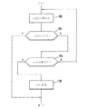
有効信号の遮断によるA/D変換器の検査のために計算要素10は対応するプログラムを有し、このプログラムが図3の流れ図に示されている。計算要素10がその出力Pxを「ハイ」レベルにセットしたとき、すなわちテスト条件が存在するとき、このプログラムが開始される。次に、第1のステップ100において入力電圧UADCが読み込まれ、それに続くステップ102において入力電圧UADCが所定の値U3と比較される。電圧値が公差範囲内で所定の値U3に等しい場合テストは終了され、出力信号Pxは再び「ロー」にセットされる。この場合、入力チャンネルは機能性を有していると判定される。読み込まれた電圧が公差範囲内で電圧値U3に対応していない場合、それに続くステップ104において、テスト過程が終了したか否かが検査される。これは所定の時間経過した後とすることが好ましく、この所定時間の経過後、計算要素10はその出力Pxを再び「ロー」にセットする。この条件が経過していない場合、ステップ100から機能検査が反復される。入力チャンネルの機能性が特定されることなくテストの終了に到達した場合、ステップ106により、例えば出力制御に関して非常運転を導くエラー応答が開始される。その後、プログラム部分は終了され、次のテスト条件が存在したとき再び開始される。
【0030】
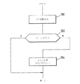
第2の入力チャンネルA2ないしマルチプレクサ32の検査のために、計算要素10は同様なプログラムを有している。このプログラムが図4に流れ図として示されている。そこに示したプログラムはマルチプレクサ32の制御に同期して所定の時点に開始される。マルチプレクサ32を介して分割電圧UTが計算要素10に供給されたとき図4に示すプログラムが開始され、第1のステップ200において電圧UTが読み込まれる。それに続くステップ202において、読み込まれた電圧が公差範囲内において抵抗R3及びR4により与えられる電圧値UT0に対応するか否かが検査される。これが肯定の場合、マルチプレクサ32ないし入力チャンネルA2が正しく作動していると判定されてプログラム部分が終了され、否定の場合ステップ204により、例えば出力制御の制限のような対応するエラー応答が開始される。ステップ204の後プログラムは終了され、次の時点において再び開始される。
【0031】
好ましい実施形態においては、エラーが複数回連続して検出されたとき、又はエラーがある頻度で検出されたときにエラー応答が開始される。
【図面の簡単な説明】
【図1】アナログ/ディジタル変換器の検査のために有効信号を遮断するための回路装置の回路図である。
【図2】アナログ/ディジタル変換器の検査のときに発生する本質的な信号の線図である。
【図3】A/Dチャンネルのモニタリングのために使用されるプログラムの流れ図である。
【図4】第2のA/Dチャンネル及び/又はその前に設けられたマルチプレクサのモニタリングのためのプログラムの流れ図である。
【符号の説明】
8 制御ユニット
10 計算要素
12 アナログ/ディジタル変換器
16 出力設定要素
20 測定装置(加速ペダル位置、ドライバの希望)
24 比較器
32 マルチプレクサ
38、40 測定装置(運転変数)[0001]
BACKGROUND OF THE INVENTION
The present invention relates to a monitor device for detecting a measurement value in engine control.
[0002]
[Prior art]
A method of this kind or a device of this kind is known from German Offenlegungsschrift 3,621,937 (US Pat. No. 5,107,427). In the description, for the detection of errors in the range of electronic power control measurement value detection, in particular in the A / D interface of the electronic control unit of the output control device or of the multiplexed A / D converter. In order to detect errors in the channel, the power control operating variables measured by the measuring device are adjusted. This is done by interrupting the earth line of the position transmitter, which is configured as an accelerator pedal and / or a throttle valve potentiometer, by means of a switching element operable from the control unit. In the shut-off state, an error condition is detected if the operating variable measured by the measuring device exceeds a predetermined limit value or a limit value derived from the read supply voltage of the measuring device.
[0003]
In particular, it has been found that the monitoring process during which engine control cannot be performed requires a relatively long time due to tolerances in the supply lines to the measuring device and the control unit. Furthermore, additional circuit means are required within the range of the switching element, especially considering the short-circuit strength of the switching element with respect to the battery voltage or supply voltage. Furthermore, the function of the channel of the analog / digital converter is certainly checked by known methods, but the function of the multiplexer provided before it is not checked.
[0004]
European Patent Publication No. 354269 provides a method and circuit arrangement for monitoring the transmission resistance of a potentiometer. In that description, the signal line level is connected to ground via a switching element by a calculation element at a given point in time, and from the values available in the calculation element regarding the potentiometer position, the voltage in the connected state and the supply voltage, The actual transfer resistance is calculated. No monitoring method and means for measuring value detection are described, so an error condition within the A / D converter of the computational element may lead to a function having an output control error.
[0005]
[Problems to be solved by the invention]
It is an object of the present invention to provide a measure for performing the most accurate monitoring of measurement value detection with little or no effect on engine control.
[0006]
[Means for Solving the Problems]
An object of the invention is to provide a calculation element, wherein the calculation element can use at least one input of an A / D converter, and various input signals are supplied to the at least one input via a multiplexer. In the method of monitoring measurement value detection in control, one of the input signals is a predetermined fixed reference voltage, and the reference voltage is read to check the functional operation of the multiplexer and / or the A / D converter. This is solved by the monitoring method of the measurement value detection in the engine control according to the present invention.
[0007]
The task also comprises a computing element having at least one analog input of an analog / digital converter, wherein the at least one analog input is provided with a valid signal that is evaluated for engine control via an input line. In a monitoring device for measurement value detection in engine control, an output line of a comparator is coupled to the input line, and the comparator is activated via the output from the computing element to output a low signal at its output. On the basis of this, the input voltage at the analog input goes to a level that exists outside the range of the measurement voltage. This is solved by the monitoring device for measurement value detection in engine control according to the present invention.
[0008]
The approach according to the invention allows reliable and accurate monitoring of the multiplexer provided before the A / D converter, the input value of the multiplexer and / or the A / D channel to which the output of the multiplexer is provided.
[0009]
The approach according to the invention makes it possible to check the A / D channel for the authenticity of the A / D converted voltage value.
[0010]
The approach according to the invention provides a circuit arrangement for interrupting the valid signal, which allows a quick and accurate examination of the analog / digital converter of the computing element.
[0011]
It is particularly advantageous that a simple circuit arrangement is used without incurring significant costs for the components.
[0012]
It is particularly advantageous if a signal is derived from the circuit arrangement and used for monitoring the second channel of the A / D converter and / or for monitoring a multiplexer provided in front of it. is there.
[0013]
In normal operation, only a small residual current flows in the circuit arrangement, and it is particularly advantageous that the effect on the effective signal due to rapid interruption is very small.
[0014]
DETAILED DESCRIPTION OF THE INVENTION
Hereinafter, the present invention will be described in detail with reference to embodiments shown in the drawings.
[0015]
FIG. 1 shows a calculation element 10 as part of an electronic control unit 8, which has an analog / digital converter (ADC) 12 with at least two input channels A1 and A2. . Via at least one
[0016]
The input circuit of the first ADC channel is configured as follows. A
[0017]
[0018]
The divided voltage is further supplied via
[0019]
The circuit arrangement shown in FIG. 1 ensures discontinuous monitoring of the A / D converter of the calculation element 10. For this purpose, at the analog input A1, the actual measured voltage UADC, which fluctuates within a predetermined range U1 or U2 during normal operation, is led to ground for a predetermined time by an external circuit or is lowered to a low voltage level . This action is performed so that the measurement voltage UADC is reduced to a level U3 that is much smaller than the lower level of the measurement signal U1. Level U3 clearly exists outside the measurement window or measurement range U2-U1. The computing element 10 controls this action via its output Px and distorts the input channel to check whether the read voltage is at the expected value. If this test is positive, the
[0020]
When the computing element 10, which is a computer, outputs a “High” signal via its output Px, the
[0021]
Therefore, in the preferred embodiment of electronic engine power control where the accelerator pedal position is measured by two redundant sensors, it is very suitable to adjust the effective signal used only for monitoring the effective signal for power control. ing. This is because at this time, an effective signal for performing output control is used as it is.
[0022]
The resistor R2 is chosen to be much smaller than R1 so that the capacitor C1 used for the smoothing of the analog signal can be discharged quickly for measurement.
[0023]
Since the residual current of the interrupted comparator is very small, the residual current has little negative effect on the valid signal U E and flows to ground (via the transistor in the comparator), so that the cable breaks However, the residual current does not generate a voltage at the resistor RP, so that the comparison made for the detection of the cable break is not disturbed.
[0024]
With this circuit arrangement, the valid signal is easily adjusted for the inspection of the A / D converter. This circuit is designed to ensure that the residual current and the quick examination of the ADC, and thus the adverse effect on the valid signal, are very small.
[0025]
Furthermore, the divided voltage UT supplied to the
[0026]
Multiplexer 32 is controlled by control element 10 via a control line, whereby various input variables E1 to En are read via input A2 and output A of multiplexer 32. The divided voltage UT is supplied as an input value via
[0027]
2A and 2B show time diagrams of essential signals. FIG. 2A shows a time diagram of the effective signal voltage UADC, while FIG. 2B shows a time diagram of the output signal Px of the calculation element 10. Until the time T 1, the output signal Px of the calculation element 10 is “low”. This means that the valid signal is not affected. Accordingly, correspondingly, the input variable U E fluctuates between the voltages U1 and U2. It is assumed that the output line of the calculation element 10 is switched to “high” at the time T 1 . In useful signal point T 1 and correspondingly, to free measurement range U1 varies to the level U3 present in sufficiently lower than U2. After the test process is completed at time T 2 , the output Px of the calculation element 10 is switched to “low” again, so that at this time, the valid signal is again set to the valid signal value UADC as shown in FIG. I will take it.
[0028]
The inspection is started when the selected test condition exists. This inspection condition is, for example, a time condition, or determined based on the driving state of the automobile and / or the engine. For example, the effective signal may be cut off when the accelerator pedal is released during the engine starting process, at a substantially constant accelerator pedal position, after a predetermined operating time has elapsed, or at predetermined time intervals.
[0029]
For the inspection of the A / D converter by the interruption of the valid signal, the calculation element 10 has a corresponding program, which is shown in the flowchart of FIG. The program is started when the computing element 10 sets its output Px to a “high” level, ie when a test condition exists. Next, in the
[0030]
For the examination of the second input channel A2 or the multiplexer 32, the computing element 10 has a similar program. This program is shown as a flow diagram in FIG. The program shown there is started at a predetermined time in synchronization with the control of the multiplexer 32. When the divided voltage UT is supplied to the calculation element 10 via the multiplexer 32, the program shown in FIG. 4 is started, and the voltage UT is read in the
[0031]
In a preferred embodiment, an error response is initiated when an error is detected multiple times in succession, or when an error is detected at a certain frequency.
[Brief description of the drawings]
FIG. 1 is a circuit diagram of a circuit device for interrupting a valid signal for inspection of an analog / digital converter.
FIG. 2 is a diagram of the essential signals that occur when testing an analog / digital converter.
FIG. 3 is a flowchart of a program used for A / D channel monitoring.
FIG. 4 is a flow chart of a program for monitoring a second A / D channel and / or a multiplexer provided in front of it.
[Explanation of symbols]
8 Control unit 10
24 Comparator 32
Claims (5)
計算要素の第1の入力は、測定電圧(UADC)を受け取り、
計算要素の第2の入力は、マルチプレクサ(32)を介して種々の入力信号を受け取り、この第2の入力の1つが固定設定基準電圧(UT)であり、
比較器(24)の出力が、計算要素(10)の第1の入力(A1)に結合され、
計算要素の前記少なくとも1つの出力(PX)を介して、比較器(24)が作動して、前記測定電圧が比較器により所定のレベルに切り換えられ、
比較器の基準値は、基準電圧(UT)であり、
計算要素が少なくとも1つの出力(PX)により比較器を作動し、
測定電圧は、A/D変換器によりディジタル化され、計算要素の所定値と比較され、
計算要素は、基準電圧(UT)を受け取って、所定値と比較し、
計算要素は、ディジタル化された測定電圧または基準電圧がそれぞれの所定値に対応していないとき、測定値検出の範囲内のエラーを特定する、
機関制御における測定値検出のモニタ装置。A computing element (10) is provided, the computing element (10) being able to utilize at least two first (A1) and second (A2) inputs of the A / D converter (12) and at least one In a monitoring device for measuring value detection in engine control, having two outputs (PX),
The first input of the calculation element receives the measured voltage (UADC)
The second input of the computing element receives various input signals via a multiplexer (32), one of which is a fixed set reference voltage (UT),
The output of the comparator (24) is coupled to the first input (A1) of the computational element (10);
Via the at least one output (PX) of the calculation element, the comparator (24) is activated, and the measured voltage is switched to a predetermined level by the comparator,
The reference value of the comparator is the reference voltage (UT),
The computational element operates the comparator with at least one output (PX);
The measured voltage is digitized by an A / D converter and compared with a predetermined value of the calculation element,
The calculation element receives the reference voltage (UT) and compares it with a predetermined value,
The calculation element identifies an error within the range of measurement detection when the digitized measurement voltage or reference voltage does not correspond to the respective predetermined value.
Monitor device for measurement value detection in engine control.
Applications Claiming Priority (2)
| Application Number | Priority Date | Filing Date | Title |
|---|---|---|---|
| DE19640937A DE19640937B4 (en) | 1996-10-04 | 1996-10-04 | Device for monitoring the measured value acquisition in a motor controller |
| DE19640937.3 | 1996-10-04 |
Publications (2)
| Publication Number | Publication Date |
|---|---|
| JPH10115247A JPH10115247A (en) | 1998-05-06 |
| JP4222648B2 true JP4222648B2 (en) | 2009-02-12 |
Family
ID=7807855
Family Applications (1)
| Application Number | Title | Priority Date | Filing Date |
|---|---|---|---|
| JP26838397A Expired - Fee Related JP4222648B2 (en) | 1996-10-04 | 1997-10-01 | Monitoring device for measurement value detection in engine control |
Country Status (5)
| Country | Link |
|---|---|
| JP (1) | JP4222648B2 (en) |
| DE (1) | DE19640937B4 (en) |
| FR (1) | FR2754312B1 (en) |
| GB (1) | GB2317969B (en) |
| IT (1) | IT1295086B1 (en) |
Families Citing this family (20)
| Publication number | Priority date | Publication date | Assignee | Title |
|---|---|---|---|---|
| US7949495B2 (en) | 1996-03-28 | 2011-05-24 | Rosemount, Inc. | Process variable transmitter with diagnostics |
| US8290721B2 (en) | 1996-03-28 | 2012-10-16 | Rosemount Inc. | Flow measurement diagnostics |
| DE19963152B4 (en) * | 1999-12-24 | 2009-06-10 | Conti Temic Microelectronic Gmbh | Method for suppressing crosstalk between multiplexer channels |
| DE10131824B4 (en) * | 2001-06-30 | 2011-09-29 | Hella Kgaa Hueck & Co. | Circuit device for failure detection of LEDs in a motor vehicle |
| DE10152216B4 (en) * | 2001-10-23 | 2006-01-26 | Siemens Ag | Method and device for monitoring a bus system |
| US7135998B2 (en) | 2002-05-08 | 2006-11-14 | Continental Teves Ag & Co. Ohg | Electronic circuit arrangement for error-free analog/digital conversion of signals |
| US7046180B2 (en) * | 2004-04-21 | 2006-05-16 | Rosemount Inc. | Analog-to-digital converter with range error detection |
| US8112565B2 (en) | 2005-06-08 | 2012-02-07 | Fisher-Rosemount Systems, Inc. | Multi-protocol field device interface with automatic bus detection |
| DE102005030276A1 (en) * | 2005-06-21 | 2006-12-28 | Pilz Gmbh & Co. Kg | Safety switching device for e.g. safe shutdown of consumer unit in automated installation has analog signal combiner, which is designed to superimpose analog test signal on analog input signal to form analog combination signal |
| US20070068225A1 (en) | 2005-09-29 | 2007-03-29 | Brown Gregory C | Leak detector for process valve |
| JP4779793B2 (en) | 2006-05-01 | 2011-09-28 | 株式会社デンソー | AD converter and electronic control device |
| US7953501B2 (en) | 2006-09-25 | 2011-05-31 | Fisher-Rosemount Systems, Inc. | Industrial process control loop monitor |
| US7750642B2 (en) | 2006-09-29 | 2010-07-06 | Rosemount Inc. | Magnetic flowmeter with verification |
| US8898036B2 (en) | 2007-08-06 | 2014-11-25 | Rosemount Inc. | Process variable transmitter with acceleration sensor |
| US9207670B2 (en) | 2011-03-21 | 2015-12-08 | Rosemount Inc. | Degrading sensor detection implemented within a transmitter |
| DE102011050539B4 (en) * | 2011-05-20 | 2014-11-20 | Phoenix Contact Gmbh & Co. Kg | Measuring device with a safe measuring channel |
| US9052240B2 (en) | 2012-06-29 | 2015-06-09 | Rosemount Inc. | Industrial process temperature transmitter with sensor stress diagnostics |
| US9602122B2 (en) | 2012-09-28 | 2017-03-21 | Rosemount Inc. | Process variable measurement noise diagnostic |
| DE102013111888B4 (en) | 2013-10-29 | 2018-06-14 | Phoenix Contact Gmbh & Co. Kg | Safety device for multi-channel processing of an analog input signal |
| DE102018008109A1 (en) * | 2018-10-12 | 2020-04-16 | WAGO Verwaltungsgesellschaft mit beschränkter Haftung | SAFETY CIRCUIT AND METHOD FOR TESTING A SAFETY CIRCUIT IN AN AUTOMATION SYSTEM |
Family Cites Families (9)
| Publication number | Priority date | Publication date | Assignee | Title |
|---|---|---|---|---|
| JPS5534817A (en) * | 1978-08-31 | 1980-03-11 | Tokyo Electric Power Co | Converter |
| US4598355A (en) * | 1983-10-27 | 1986-07-01 | Sundstrand Corporation | Fault tolerant controller |
| DE3621937A1 (en) * | 1986-06-30 | 1988-01-07 | Bosch Gmbh Robert | MONITORING DEVICE FOR AN ELECTRONIC CONTROL DEVICE IN A MOTOR VEHICLE |
| JPH01219903A (en) * | 1988-02-26 | 1989-09-01 | Fujitsu Ten Ltd | Method for generating signal at the time of trouble of electronic control circuit and evaluating method for this trouble |
| DE3826937A1 (en) * | 1988-08-09 | 1990-02-15 | Vdo Schindling | METHOD AND CIRCUIT ARRANGEMENT FOR MONITORING THE TRANSITION RESISTANCE IN A POTENTIOMETER serving as a position encoder |
| JPH03233160A (en) * | 1990-02-08 | 1991-10-17 | Mitsubishi Electric Corp | Control device of engine |
| JP2844815B2 (en) * | 1990-03-16 | 1999-01-13 | 株式会社デンソー | Vehicle electronic control unit |
| JPH03268610A (en) * | 1990-03-19 | 1991-11-29 | Nec Corp | Analog/digital converter |
| JPH06181434A (en) * | 1992-12-14 | 1994-06-28 | Hitachi Ltd | Fault detection system for a/d converter |
-
1996
- 1996-10-04 DE DE19640937A patent/DE19640937B4/en not_active Expired - Lifetime
-
1997
- 1997-09-23 FR FR9711803A patent/FR2754312B1/en not_active Expired - Fee Related
- 1997-09-24 GB GB9720330A patent/GB2317969B/en not_active Expired - Fee Related
- 1997-09-26 IT ITMI972192 patent/IT1295086B1/en active IP Right Grant
- 1997-10-01 JP JP26838397A patent/JP4222648B2/en not_active Expired - Fee Related
Also Published As
| Publication number | Publication date |
|---|---|
| FR2754312A1 (en) | 1998-04-10 |
| DE19640937B4 (en) | 2013-11-28 |
| FR2754312B1 (en) | 2002-10-18 |
| DE19640937A1 (en) | 1998-04-09 |
| GB2317969B (en) | 1999-02-10 |
| GB9720330D0 (en) | 1997-11-26 |
| ITMI972192A1 (en) | 1999-03-26 |
| IT1295086B1 (en) | 1999-04-27 |
| JPH10115247A (en) | 1998-05-06 |
| GB2317969A (en) | 1998-04-08 |
Similar Documents
| Publication | Publication Date | Title |
|---|---|---|
| JP4222648B2 (en) | Monitoring device for measurement value detection in engine control | |
| US5404304A (en) | Vehicle control system for determining verified wheel speed signals | |
| US8180520B2 (en) | Electronic safing system | |
| US5459732A (en) | Method and apparatus for anti-lock brake single channel wheel speed processing with diagnosis | |
| US7573275B2 (en) | Temperature sensor control apparatus | |
| US5406485A (en) | Method and apparatus for detecting faulty operation of a wheel speed sensor | |
| US4783631A (en) | Apparatus for detecting disconnection of a speed sensor and eliminating oxide film from the sensor's connectors | |
| US5327780A (en) | Method and arrangement for monitoring the operability of a heater of an oxygen measuring probe | |
| US6912887B2 (en) | Oxygen sensor abnormality detecting device having offset voltage circuit | |
| JP2004090920A (en) | Method and device for detecting variable amount of vehicle | |
| JP2844815B2 (en) | Vehicle electronic control unit | |
| US7002352B2 (en) | Reference voltage diagnostic suitable for use in an automobile controller and method therefor | |
| JPH10501599A (en) | Method and apparatus for monitoring measured value detection in vehicle engine electronic power control | |
| JPH1183791A (en) | Function monitoring method and apparatus for gas sensor, especially lambda sensor for internal combustion engine | |
| JP3188327B2 (en) | Oxygen sensor connection circuit and correct sensor connection inspection method | |
| CN111751757A (en) | Fault detection circuit and method for vehicle-mounted indicator lamp | |
| JPH10332759A (en) | Electric circuit device and inspection method thereof | |
| KR101601756B1 (en) | Method for diagnosing disconnection of oxygen sensor and apparatus thereof | |
| US20170363481A1 (en) | Fault Detection Apparatus | |
| JP7055873B2 (en) | In-vehicle electronic control device | |
| KR0158162B1 (en) | Disorder decision system of a coolant temperature sensor | |
| JPH02165069A (en) | Abnormality detector for electric circuit | |
| JPH07198659A (en) | Method and equipment for fault detection of exhaust gas oxygen senser | |
| US10790685B2 (en) | Measurement apparatus and on-board battery charger | |
| KR19980049818A (en) | Fuel supply diagnosis device and method |
Legal Events
| Date | Code | Title | Description |
|---|---|---|---|
| A621 | Written request for application examination |
Free format text: JAPANESE INTERMEDIATE CODE: A621 Effective date: 20040915 |
|
| A131 | Notification of reasons for refusal |
Free format text: JAPANESE INTERMEDIATE CODE: A131 Effective date: 20070105 |
|
| A601 | Written request for extension of time |
Free format text: JAPANESE INTERMEDIATE CODE: A601 Effective date: 20070109 |
|
| A602 | Written permission of extension of time |
Free format text: JAPANESE INTERMEDIATE CODE: A602 Effective date: 20070112 |
|
| A521 | Written amendment |
Free format text: JAPANESE INTERMEDIATE CODE: A523 Effective date: 20070530 |
|
| A131 | Notification of reasons for refusal |
Free format text: JAPANESE INTERMEDIATE CODE: A131 Effective date: 20071204 |
|
| A601 | Written request for extension of time |
Free format text: JAPANESE INTERMEDIATE CODE: A601 Effective date: 20080303 |
|
| A602 | Written permission of extension of time |
Free format text: JAPANESE INTERMEDIATE CODE: A602 Effective date: 20080306 |
|
| A521 | Written amendment |
Free format text: JAPANESE INTERMEDIATE CODE: A523 Effective date: 20080521 |
|
| TRDD | Decision of grant or rejection written | ||
| A01 | Written decision to grant a patent or to grant a registration (utility model) |
Free format text: JAPANESE INTERMEDIATE CODE: A01 Effective date: 20081021 |
|
| A01 | Written decision to grant a patent or to grant a registration (utility model) |
Free format text: JAPANESE INTERMEDIATE CODE: A01 |
|
| A61 | First payment of annual fees (during grant procedure) |
Free format text: JAPANESE INTERMEDIATE CODE: A61 Effective date: 20081118 |
|
| R150 | Certificate of patent (=grant) or registration of utility model |
Free format text: JAPANESE INTERMEDIATE CODE: R150 |
|
| FPAY | Renewal fee payment (prs date is renewal date of database) |
Free format text: PAYMENT UNTIL: 20111128 Year of fee payment: 3 |
|
| FPAY | Renewal fee payment (prs date is renewal date of database) |
Free format text: PAYMENT UNTIL: 20121128 Year of fee payment: 4 |
|
| FPAY | Renewal fee payment (prs date is renewal date of database) |
Free format text: PAYMENT UNTIL: 20131128 Year of fee payment: 5 |
|
| LAPS | Cancellation because of no payment of annual fees |