JP4213616B2 - Base film for liquid crystal panel, functional film for liquid crystal panel, method for producing functional film, and apparatus for producing functional film - Google Patents
Base film for liquid crystal panel, functional film for liquid crystal panel, method for producing functional film, and apparatus for producing functional film Download PDFInfo
- Publication number
- JP4213616B2 JP4213616B2 JP2004106457A JP2004106457A JP4213616B2 JP 4213616 B2 JP4213616 B2 JP 4213616B2 JP 2004106457 A JP2004106457 A JP 2004106457A JP 2004106457 A JP2004106457 A JP 2004106457A JP 4213616 B2 JP4213616 B2 JP 4213616B2
- Authority
- JP
- Japan
- Prior art keywords
- film
- functional
- group
- liquid crystal
- thin film
- Prior art date
- Legal status (The legal status is an assumption and is not a legal conclusion. Google has not performed a legal analysis and makes no representation as to the accuracy of the status listed.)
- Expired - Fee Related
Links
- 239000004973 liquid crystal related substance Substances 0.000 title claims description 381
- 238000004519 manufacturing process Methods 0.000 title description 100
- 239000010408 film Substances 0.000 claims description 1347
- 239000010410 layer Substances 0.000 claims description 390
- 239000000758 substrate Substances 0.000 claims description 298
- 238000000034 method Methods 0.000 claims description 291
- 239000010409 thin film Substances 0.000 claims description 281
- 239000002585 base Substances 0.000 claims description 216
- 229920005989 resin Polymers 0.000 claims description 184
- 239000011347 resin Substances 0.000 claims description 184
- 239000000463 material Substances 0.000 claims description 132
- 230000006870 function Effects 0.000 claims description 126
- 230000003287 optical effect Effects 0.000 claims description 107
- 239000013039 cover film Substances 0.000 claims description 90
- 238000012546 transfer Methods 0.000 claims description 90
- 238000000576 coating method Methods 0.000 claims description 89
- -1 polyethylene Polymers 0.000 claims description 86
- 230000004888 barrier function Effects 0.000 claims description 62
- 239000000203 mixture Substances 0.000 claims description 60
- 238000002834 transmittance Methods 0.000 claims description 54
- 239000007789 gas Substances 0.000 claims description 49
- 230000001681 protective effect Effects 0.000 claims description 47
- 239000011368 organic material Substances 0.000 claims description 44
- 229920000178 Acrylic resin Polymers 0.000 claims description 41
- 239000004925 Acrylic resin Substances 0.000 claims description 41
- 239000000853 adhesive Substances 0.000 claims description 41
- 229910052782 aluminium Inorganic materials 0.000 claims description 39
- 239000012071 phase Substances 0.000 claims description 39
- VYPSYNLAJGMNEJ-UHFFFAOYSA-N Silicium dioxide Chemical compound O=[Si]=O VYPSYNLAJGMNEJ-UHFFFAOYSA-N 0.000 claims description 36
- 230000001070 adhesive effect Effects 0.000 claims description 36
- 150000001875 compounds Chemical class 0.000 claims description 36
- 229920001721 polyimide Polymers 0.000 claims description 36
- 230000008859 change Effects 0.000 claims description 34
- 229920001577 copolymer Polymers 0.000 claims description 33
- 239000011159 matrix material Substances 0.000 claims description 33
- XAGFODPZIPBFFR-UHFFFAOYSA-N aluminium Chemical compound [Al] XAGFODPZIPBFFR-UHFFFAOYSA-N 0.000 claims description 31
- 239000011256 inorganic filler Substances 0.000 claims description 31
- 229910003475 inorganic filler Inorganic materials 0.000 claims description 31
- 239000000975 dye Substances 0.000 claims description 29
- 229910052751 metal Inorganic materials 0.000 claims description 29
- 239000002184 metal Substances 0.000 claims description 29
- 239000004372 Polyvinyl alcohol Substances 0.000 claims description 28
- 230000015572 biosynthetic process Effects 0.000 claims description 28
- 229920000642 polymer Polymers 0.000 claims description 28
- 229920002451 polyvinyl alcohol Polymers 0.000 claims description 28
- 229910052814 silicon oxide Inorganic materials 0.000 claims description 28
- 125000003118 aryl group Chemical group 0.000 claims description 26
- 229910052760 oxygen Inorganic materials 0.000 claims description 24
- 239000002245 particle Substances 0.000 claims description 24
- 239000000126 substance Substances 0.000 claims description 24
- 239000004642 Polyimide Substances 0.000 claims description 23
- 239000004760 aramid Substances 0.000 claims description 23
- 229920003235 aromatic polyamide Polymers 0.000 claims description 23
- 125000004435 hydrogen atom Chemical group [H]* 0.000 claims description 22
- 229920005672 polyolefin resin Polymers 0.000 claims description 22
- QVGXLLKOCUKJST-UHFFFAOYSA-N atomic oxygen Chemical compound [O] QVGXLLKOCUKJST-UHFFFAOYSA-N 0.000 claims description 21
- 239000001301 oxygen Substances 0.000 claims description 21
- XLOMVQKBTHCTTD-UHFFFAOYSA-N Zinc monoxide Chemical compound [Zn]=O XLOMVQKBTHCTTD-UHFFFAOYSA-N 0.000 claims description 20
- 125000004122 cyclic group Chemical group 0.000 claims description 20
- 229920000139 polyethylene terephthalate Polymers 0.000 claims description 20
- 239000005020 polyethylene terephthalate Substances 0.000 claims description 20
- 239000002734 clay mineral Substances 0.000 claims description 19
- OTTZHAVKAVGASB-UHFFFAOYSA-N hept-2-ene Chemical compound CCCCC=CC OTTZHAVKAVGASB-UHFFFAOYSA-N 0.000 claims description 18
- VGGSQFUCUMXWEO-UHFFFAOYSA-N Ethene Chemical compound C=C VGGSQFUCUMXWEO-UHFFFAOYSA-N 0.000 claims description 17
- 239000005977 Ethylene Substances 0.000 claims description 17
- NIXOWILDQLNWCW-UHFFFAOYSA-N acrylic acid group Chemical group C(C=C)(=O)O NIXOWILDQLNWCW-UHFFFAOYSA-N 0.000 claims description 17
- 125000003178 carboxy group Chemical group [H]OC(*)=O 0.000 claims description 16
- 238000009792 diffusion process Methods 0.000 claims description 16
- 239000011777 magnesium Substances 0.000 claims description 16
- 229910052749 magnesium Inorganic materials 0.000 claims description 16
- 125000002496 methyl group Chemical group [H]C([H])([H])* 0.000 claims description 16
- XLYOFNOQVPJJNP-UHFFFAOYSA-N water Chemical compound O XLYOFNOQVPJJNP-UHFFFAOYSA-N 0.000 claims description 16
- 125000000217 alkyl group Chemical group 0.000 claims description 15
- 229920000728 polyester Polymers 0.000 claims description 15
- ZCYVEMRRCGMTRW-UHFFFAOYSA-N 7553-56-2 Chemical compound [I] ZCYVEMRRCGMTRW-UHFFFAOYSA-N 0.000 claims description 14
- 239000004952 Polyamide Substances 0.000 claims description 14
- 125000005843 halogen group Chemical group 0.000 claims description 14
- 230000005525 hole transport Effects 0.000 claims description 14
- 229910052740 iodine Inorganic materials 0.000 claims description 14
- 239000011630 iodine Substances 0.000 claims description 14
- 229920002647 polyamide Polymers 0.000 claims description 14
- 229910018072 Al 2 O 3 Inorganic materials 0.000 claims description 13
- JRZJOMJEPLMPRA-UHFFFAOYSA-N olefin Natural products CCCCCCCC=C JRZJOMJEPLMPRA-UHFFFAOYSA-N 0.000 claims description 13
- FYYHWMGAXLPEAU-UHFFFAOYSA-N Magnesium Chemical compound [Mg] FYYHWMGAXLPEAU-UHFFFAOYSA-N 0.000 claims description 12
- 239000004698 Polyethylene Substances 0.000 claims description 12
- 229920000573 polyethylene Polymers 0.000 claims description 12
- NIXOWILDQLNWCW-UHFFFAOYSA-M Acrylate Chemical compound [O-]C(=O)C=C NIXOWILDQLNWCW-UHFFFAOYSA-M 0.000 claims description 11
- 239000004743 Polypropylene Substances 0.000 claims description 11
- PNEYBMLMFCGWSK-UHFFFAOYSA-N aluminium oxide Inorganic materials [O-2].[O-2].[O-2].[Al+3].[Al+3] PNEYBMLMFCGWSK-UHFFFAOYSA-N 0.000 claims description 11
- 239000003822 epoxy resin Substances 0.000 claims description 11
- 125000002887 hydroxy group Chemical group [H]O* 0.000 claims description 11
- 229920000647 polyepoxide Polymers 0.000 claims description 11
- 229920001225 polyester resin Polymers 0.000 claims description 11
- 239000004645 polyester resin Substances 0.000 claims description 11
- 229920001155 polypropylene Polymers 0.000 claims description 11
- 229910004298 SiO 2 Inorganic materials 0.000 claims description 10
- 125000003545 alkoxy group Chemical group 0.000 claims description 10
- 125000001424 substituent group Chemical group 0.000 claims description 10
- 239000011787 zinc oxide Substances 0.000 claims description 10
- 125000004093 cyano group Chemical group *C#N 0.000 claims description 9
- 239000009719 polyimide resin Substances 0.000 claims description 9
- 230000003595 spectral effect Effects 0.000 claims description 9
- CERQOIWHTDAKMF-UHFFFAOYSA-M Methacrylate Chemical compound CC(=C)C([O-])=O CERQOIWHTDAKMF-UHFFFAOYSA-M 0.000 claims description 8
- 230000005540 biological transmission Effects 0.000 claims description 8
- PHCKFVVLVZFFLU-UHFFFAOYSA-N dodec-4-ene Chemical compound CCCCCCCC=CCCC PHCKFVVLVZFFLU-UHFFFAOYSA-N 0.000 claims description 8
- GWEVSGVZZGPLCZ-UHFFFAOYSA-N Titan oxide Chemical compound O=[Ti]=O GWEVSGVZZGPLCZ-UHFFFAOYSA-N 0.000 claims description 7
- 239000001000 anthraquinone dye Substances 0.000 claims description 7
- 239000000987 azo dye Substances 0.000 claims description 7
- 230000001588 bifunctional effect Effects 0.000 claims description 7
- 125000004432 carbon atom Chemical group C* 0.000 claims description 7
- 238000003475 lamination Methods 0.000 claims description 7
- 125000000449 nitro group Chemical group [O-][N+](*)=O 0.000 claims description 7
- TWNQGVIAIRXVLR-UHFFFAOYSA-N oxo(oxoalumanyloxy)alumane Chemical compound O=[Al]O[Al]=O TWNQGVIAIRXVLR-UHFFFAOYSA-N 0.000 claims description 7
- 125000001997 phenyl group Chemical group [H]C1=C([H])C([H])=C(*)C([H])=C1[H] 0.000 claims description 7
- 229920005668 polycarbonate resin Polymers 0.000 claims description 7
- 239000004431 polycarbonate resin Substances 0.000 claims description 7
- 125000000753 cycloalkyl group Chemical group 0.000 claims description 6
- 229910052739 hydrogen Inorganic materials 0.000 claims description 6
- 125000000956 methoxy group Chemical group [H]C([H])([H])O* 0.000 claims description 6
- 125000000587 piperidin-1-yl group Chemical group [H]C1([H])N(*)C([H])([H])C([H])([H])C([H])([H])C1([H])[H] 0.000 claims description 6
- 229920006122 polyamide resin Polymers 0.000 claims description 6
- 229920013716 polyethylene resin Polymers 0.000 claims description 6
- 229910052709 silver Inorganic materials 0.000 claims description 6
- HRPVXLWXLXDGHG-UHFFFAOYSA-N Acrylamide Chemical group NC(=O)C=C HRPVXLWXLXDGHG-UHFFFAOYSA-N 0.000 claims description 5
- 229910017083 AlN Inorganic materials 0.000 claims description 5
- 229910004541 SiN Inorganic materials 0.000 claims description 5
- HVVWZTWDBSEWIH-UHFFFAOYSA-N [2-(hydroxymethyl)-3-prop-2-enoyloxy-2-(prop-2-enoyloxymethyl)propyl] prop-2-enoate Chemical compound C=CC(=O)OCC(CO)(COC(=O)C=C)COC(=O)C=C HVVWZTWDBSEWIH-UHFFFAOYSA-N 0.000 claims description 5
- DQXBYHZEEUGOBF-UHFFFAOYSA-N but-3-enoic acid;ethene Chemical compound C=C.OC(=O)CC=C DQXBYHZEEUGOBF-UHFFFAOYSA-N 0.000 claims description 5
- 239000005038 ethylene vinyl acetate Substances 0.000 claims description 5
- 125000003983 fluorenyl group Chemical group C1(=CC=CC=2C3=CC=CC=C3CC12)* 0.000 claims description 5
- 229920001200 poly(ethylene-vinyl acetate) Polymers 0.000 claims description 5
- 229920002492 poly(sulfone) Polymers 0.000 claims description 5
- 229920006254 polymer film Polymers 0.000 claims description 5
- 238000003860 storage Methods 0.000 claims description 5
- OGIDPMRJRNCKJF-UHFFFAOYSA-N titanium oxide Inorganic materials [Ti]=O OGIDPMRJRNCKJF-UHFFFAOYSA-N 0.000 claims description 5
- 125000000391 vinyl group Chemical group [H]C([*])=C([H])[H] 0.000 claims description 5
- ZAMOUSCENKQFHK-UHFFFAOYSA-N Chlorine atom Chemical compound [Cl] ZAMOUSCENKQFHK-UHFFFAOYSA-N 0.000 claims description 4
- UFHFLCQGNIYNRP-UHFFFAOYSA-N Hydrogen Chemical compound [H][H] UFHFLCQGNIYNRP-UHFFFAOYSA-N 0.000 claims description 4
- 239000004962 Polyamide-imide Substances 0.000 claims description 4
- BQCADISMDOOEFD-UHFFFAOYSA-N Silver Chemical compound [Ag] BQCADISMDOOEFD-UHFFFAOYSA-N 0.000 claims description 4
- FHLPGTXWCFQMIU-UHFFFAOYSA-N [4-[2-(4-prop-2-enoyloxyphenyl)propan-2-yl]phenyl] prop-2-enoate Chemical compound C=1C=C(OC(=O)C=C)C=CC=1C(C)(C)C1=CC=C(OC(=O)C=C)C=C1 FHLPGTXWCFQMIU-UHFFFAOYSA-N 0.000 claims description 4
- 125000000609 carbazolyl group Chemical class C1(=CC=CC=2C3=CC=CC=C3NC12)* 0.000 claims description 4
- 239000000460 chlorine Substances 0.000 claims description 4
- 229910052801 chlorine Inorganic materials 0.000 claims description 4
- ZUOUZKKEUPVFJK-UHFFFAOYSA-N diphenyl Chemical class C1=CC=CC=C1C1=CC=CC=C1 ZUOUZKKEUPVFJK-UHFFFAOYSA-N 0.000 claims description 4
- 125000001495 ethyl group Chemical group [H]C([H])([H])C([H])([H])* 0.000 claims description 4
- 229910052737 gold Inorganic materials 0.000 claims description 4
- 239000001257 hydrogen Substances 0.000 claims description 4
- AMGQUBHHOARCQH-UHFFFAOYSA-N indium;oxotin Chemical compound [In].[Sn]=O AMGQUBHHOARCQH-UHFFFAOYSA-N 0.000 claims description 4
- 230000036961 partial effect Effects 0.000 claims description 4
- 230000002093 peripheral effect Effects 0.000 claims description 4
- 229920002312 polyamide-imide Polymers 0.000 claims description 4
- 239000004332 silver Substances 0.000 claims description 4
- MYWOJODOMFBVCB-UHFFFAOYSA-N 1,2,6-trimethylphenanthrene Chemical compound CC1=CC=C2C3=CC(C)=CC=C3C=CC2=C1C MYWOJODOMFBVCB-UHFFFAOYSA-N 0.000 claims description 3
- LAZHUUGOLCHESB-UHFFFAOYSA-N 2,3-dimethylbicyclo[2.2.1]hept-5-ene Chemical compound C1C2C(C)C(C)C1C=C2 LAZHUUGOLCHESB-UHFFFAOYSA-N 0.000 claims description 3
- GVNVAWHJIKLAGL-UHFFFAOYSA-N 2-(cyclohexen-1-yl)cyclohexan-1-one Chemical compound O=C1CCCCC1C1=CCCCC1 GVNVAWHJIKLAGL-UHFFFAOYSA-N 0.000 claims description 3
- AGEXUCKZTAUZJM-UHFFFAOYSA-N 2-[4,6-bis[2-(2-methylprop-2-enoyloxy)ethyl]-1,3,5-triazin-2-yl]ethyl 2-methylprop-2-enoate Chemical compound CC(=C)C(=O)OCCC1=NC(CCOC(=O)C(C)=C)=NC(CCOC(=O)C(C)=C)=N1 AGEXUCKZTAUZJM-UHFFFAOYSA-N 0.000 claims description 3
- VPWNQTHUCYMVMZ-UHFFFAOYSA-N 4,4'-sulfonyldiphenol Chemical compound C1=CC(O)=CC=C1S(=O)(=O)C1=CC=C(O)C=C1 VPWNQTHUCYMVMZ-UHFFFAOYSA-N 0.000 claims description 3
- LVXDMUDXBUNBQY-UHFFFAOYSA-N 5-cyclohexylbicyclo[2.2.1]hept-2-ene Chemical compound C1=CC2CC1CC2C1CCCCC1 LVXDMUDXBUNBQY-UHFFFAOYSA-N 0.000 claims description 3
- IZSHZLKNFQAAKX-UHFFFAOYSA-N 5-cyclopenta-2,4-dien-1-ylcyclopenta-1,3-diene Chemical group C1=CC=CC1C1C=CC=C1 IZSHZLKNFQAAKX-UHFFFAOYSA-N 0.000 claims description 3
- IGNVRWAKFRBXGF-UHFFFAOYSA-N 5-ethyl-5-methylbicyclo[2.2.1]hept-2-ene Chemical compound C1C2C(CC)(C)CC1C=C2 IGNVRWAKFRBXGF-UHFFFAOYSA-N 0.000 claims description 3
- WMWDGZLDLRCDRG-UHFFFAOYSA-N 5-hexylbicyclo[2.2.1]hept-2-ene Chemical compound C1C2C(CCCCCC)CC1C=C2 WMWDGZLDLRCDRG-UHFFFAOYSA-N 0.000 claims description 3
- PCBPVYHMZBWMAZ-UHFFFAOYSA-N 5-methylbicyclo[2.2.1]hept-2-ene Chemical compound C1C2C(C)CC1C=C2 PCBPVYHMZBWMAZ-UHFFFAOYSA-N 0.000 claims description 3
- SSNJBXJCHBXUTM-UHFFFAOYSA-N 5-methylbicyclo[2.2.1]hept-2-ene;2-methylprop-2-enoic acid Chemical compound CC(=C)C(O)=O.C1C2C(C)CC1C=C2 SSNJBXJCHBXUTM-UHFFFAOYSA-N 0.000 claims description 3
- PGNNHYNYFLXKDZ-UHFFFAOYSA-N 5-phenylbicyclo[2.2.1]hept-2-ene Chemical compound C1=CC2CC1CC2C1=CC=CC=C1 PGNNHYNYFLXKDZ-UHFFFAOYSA-N 0.000 claims description 3
- AKHDGSRSWWFVIZ-UHFFFAOYSA-N 5-propylbicyclo[2.2.1]hept-2-ene Chemical compound C1C2C(CCC)CC1C=C2 AKHDGSRSWWFVIZ-UHFFFAOYSA-N 0.000 claims description 3
- WKBOTKDWSSQWDR-UHFFFAOYSA-N Bromine atom Chemical compound [Br] WKBOTKDWSSQWDR-UHFFFAOYSA-N 0.000 claims description 3
- 101150065749 Churc1 gene Proteins 0.000 claims description 3
- DGAQECJNVWCQMB-PUAWFVPOSA-M Ilexoside XXIX Chemical group C[C@@H]1CC[C@@]2(CC[C@@]3(C(=CC[C@H]4[C@]3(CC[C@@H]5[C@@]4(CC[C@@H](C5(C)C)OS(=O)(=O)[O-])C)C)[C@@H]2[C@]1(C)O)C)C(=O)O[C@H]6[C@@H]([C@H]([C@@H]([C@H](O6)CO)O)O)O.[Na+] DGAQECJNVWCQMB-PUAWFVPOSA-M 0.000 claims description 3
- 229910000799 K alloy Inorganic materials 0.000 claims description 3
- WHXSMMKQMYFTQS-UHFFFAOYSA-N Lithium Chemical compound [Li] WHXSMMKQMYFTQS-UHFFFAOYSA-N 0.000 claims description 3
- 102100038239 Protein Churchill Human genes 0.000 claims description 3
- QYKIQEUNHZKYBP-UHFFFAOYSA-N Vinyl ether Chemical group C=COC=C QYKIQEUNHZKYBP-UHFFFAOYSA-N 0.000 claims description 3
- JUDXBRVLWDGRBC-UHFFFAOYSA-N [2-(hydroxymethyl)-3-(2-methylprop-2-enoyloxy)-2-(2-methylprop-2-enoyloxymethyl)propyl] 2-methylprop-2-enoate Chemical compound CC(=C)C(=O)OCC(CO)(COC(=O)C(C)=C)COC(=O)C(C)=C JUDXBRVLWDGRBC-UHFFFAOYSA-N 0.000 claims description 3
- 125000003647 acryloyl group Chemical group O=C([*])C([H])=C([H])[H] 0.000 claims description 3
- 229910052783 alkali metal Inorganic materials 0.000 claims description 3
- 150000001340 alkali metals Chemical group 0.000 claims description 3
- 125000003342 alkenyl group Chemical group 0.000 claims description 3
- 125000003302 alkenyloxy group Chemical group 0.000 claims description 3
- 125000003277 amino group Chemical group 0.000 claims description 3
- GDTBXPJZTBHREO-UHFFFAOYSA-N bromine Substances BrBr GDTBXPJZTBHREO-UHFFFAOYSA-N 0.000 claims description 3
- 229910052794 bromium Inorganic materials 0.000 claims description 3
- 150000001907 coumarones Chemical class 0.000 claims description 3
- GVRWIAHBVAYKIZ-UHFFFAOYSA-N dec-3-ene Chemical compound CCCCCCC=CCC GVRWIAHBVAYKIZ-UHFFFAOYSA-N 0.000 claims description 3
- DKAKUAXJPGSBIL-UHFFFAOYSA-N dimethoxy-(5-methyl-1-bicyclo[2.2.1]hept-2-enyl)silane Chemical compound CC1C2C=CC(C1)(C2)[SiH](OC)OC DKAKUAXJPGSBIL-UHFFFAOYSA-N 0.000 claims description 3
- 125000001301 ethoxy group Chemical group [H]C([H])([H])C([H])([H])O* 0.000 claims description 3
- 229910052731 fluorine Inorganic materials 0.000 claims description 3
- 239000011737 fluorine Substances 0.000 claims description 3
- 125000002485 formyl group Chemical group [H]C(*)=O 0.000 claims description 3
- 229910052738 indium Inorganic materials 0.000 claims description 3
- APFVFJFRJDLVQX-UHFFFAOYSA-N indium atom Chemical compound [In] APFVFJFRJDLVQX-UHFFFAOYSA-N 0.000 claims description 3
- 125000003253 isopropoxy group Chemical group [H]C([H])([H])C([H])(O*)C([H])([H])[H] 0.000 claims description 3
- CDOSHBSSFJOMGT-UHFFFAOYSA-N linalool Chemical compound CC(C)=CCCC(C)(O)C=C CDOSHBSSFJOMGT-UHFFFAOYSA-N 0.000 claims description 3
- 229910052744 lithium Inorganic materials 0.000 claims description 3
- JFNLZVQOOSMTJK-KNVOCYPGSA-N norbornene Chemical compound C1[C@@H]2CC[C@H]1C=C2 JFNLZVQOOSMTJK-KNVOCYPGSA-N 0.000 claims description 3
- 125000000951 phenoxy group Chemical group [H]C1=C([H])C([H])=C(O*)C([H])=C1[H] 0.000 claims description 3
- BITYAPCSNKJESK-UHFFFAOYSA-N potassiosodium Chemical compound [Na].[K] BITYAPCSNKJESK-UHFFFAOYSA-N 0.000 claims description 3
- 125000002572 propoxy group Chemical group [*]OC([H])([H])C(C([H])([H])[H])([H])[H] 0.000 claims description 3
- 125000001436 propyl group Chemical group [H]C([*])([H])C([H])([H])C([H])([H])[H] 0.000 claims description 3
- 229910052761 rare earth metal Inorganic materials 0.000 claims description 3
- 150000002910 rare earth metals Chemical class 0.000 claims description 3
- 238000007142 ring opening reaction Methods 0.000 claims description 3
- 239000011734 sodium Substances 0.000 claims description 3
- 229910052708 sodium Inorganic materials 0.000 claims description 3
- 125000005504 styryl group Chemical group 0.000 claims description 3
- 125000001273 sulfonato group Chemical group [O-]S(*)(=O)=O 0.000 claims description 3
- 150000003577 thiophenes Chemical class 0.000 claims description 3
- 125000002023 trifluoromethyl group Chemical group FC(F)(F)* 0.000 claims description 3
- YVTHLONGBIQYBO-UHFFFAOYSA-N zinc indium(3+) oxygen(2-) Chemical compound [O--].[Zn++].[In+3] YVTHLONGBIQYBO-UHFFFAOYSA-N 0.000 claims description 3
- WPNNTDKIBHJWAU-UHFFFAOYSA-N 3-(5-bicyclo[2.2.1]hept-2-enyloxymethyl)-3-ethyloxetane Chemical compound C1C(C=C2)CC2C1OCC1(CC)COC1 WPNNTDKIBHJWAU-UHFFFAOYSA-N 0.000 claims description 2
- QHDMCJQYXBCEPR-UHFFFAOYSA-N 5-methylbicyclo[2.2.1]hept-2-ene;prop-2-enoic acid Chemical compound OC(=O)C=C.C1C2C(C)CC1C=C2 QHDMCJQYXBCEPR-UHFFFAOYSA-N 0.000 claims description 2
- LSNNMFCWUKXFEE-UHFFFAOYSA-M Bisulfite Chemical compound OS([O-])=O LSNNMFCWUKXFEE-UHFFFAOYSA-M 0.000 claims description 2
- 229910021595 Copper(I) iodide Inorganic materials 0.000 claims description 2
- PXGOKWXKJXAPGV-UHFFFAOYSA-N Fluorine Chemical compound FF PXGOKWXKJXAPGV-UHFFFAOYSA-N 0.000 claims description 2
- 229910005191 Ga 2 O 3 Inorganic materials 0.000 claims description 2
- 229910006404 SnO 2 Inorganic materials 0.000 claims description 2
- QUZSUMLPWDHKCJ-UHFFFAOYSA-N bisphenol A dimethacrylate Chemical compound C1=CC(OC(=O)C(=C)C)=CC=C1C(C)(C)C1=CC=C(OC(=O)C(C)=C)C=C1 QUZSUMLPWDHKCJ-UHFFFAOYSA-N 0.000 claims description 2
- 125000001511 cyclopentyl group Chemical group [H]C1([H])C([H])([H])C([H])([H])C([H])(*)C1([H])[H] 0.000 claims description 2
- VGQLNJWOULYVFV-UHFFFAOYSA-N dimethyl bicyclo[2.2.1]hept-5-ene-2,3-dicarboxylate Chemical compound C1C2C=CC1C(C(=O)OC)C2C(=O)OC VGQLNJWOULYVFV-UHFFFAOYSA-N 0.000 claims description 2
- AEBDJCUTXUYLDC-UHFFFAOYSA-N methyl 5-methylbicyclo[2.2.1]hept-2-ene-5-carboxylate Chemical compound C1C2C(C(=O)OC)(C)CC1C=C2 AEBDJCUTXUYLDC-UHFFFAOYSA-N 0.000 claims description 2
- 238000005234 chemical deposition Methods 0.000 claims 2
- WLTSXAIICPDFKI-FNORWQNLSA-N (E)-3-dodecene Chemical compound CCCCCCCC\C=C\CC WLTSXAIICPDFKI-FNORWQNLSA-N 0.000 claims 1
- BPXVHIRIPLPOPT-UHFFFAOYSA-N 1,3,5-tris(2-hydroxyethyl)-1,3,5-triazinane-2,4,6-trione Chemical compound OCCN1C(=O)N(CCO)C(=O)N(CCO)C1=O BPXVHIRIPLPOPT-UHFFFAOYSA-N 0.000 claims 1
- WSFSSNUMVMOOMR-UHFFFAOYSA-N Formaldehyde Chemical compound O=C WSFSSNUMVMOOMR-UHFFFAOYSA-N 0.000 claims 1
- IAQRGUVFOMOMEM-UHFFFAOYSA-N butene Natural products CC=CC IAQRGUVFOMOMEM-UHFFFAOYSA-N 0.000 claims 1
- 235000019256 formaldehyde Nutrition 0.000 claims 1
- 125000004184 methoxymethyl group Chemical group [H]C([H])([H])OC([H])([H])* 0.000 claims 1
- 125000005487 naphthalate group Chemical group 0.000 claims 1
- 238000005289 physical deposition Methods 0.000 claims 1
- IAQRGUVFOMOMEM-ONEGZZNKSA-N trans-but-2-ene Chemical compound C\C=C\C IAQRGUVFOMOMEM-ONEGZZNKSA-N 0.000 claims 1
- 239000011521 glass Substances 0.000 description 68
- 239000011248 coating agent Substances 0.000 description 59
- 230000008569 process Effects 0.000 description 51
- 238000010030 laminating Methods 0.000 description 44
- 239000000243 solution Substances 0.000 description 35
- 239000000178 monomer Substances 0.000 description 32
- 239000002904 solvent Substances 0.000 description 31
- 238000010438 heat treatment Methods 0.000 description 29
- 229920003023 plastic Polymers 0.000 description 26
- 238000001035 drying Methods 0.000 description 25
- 238000005530 etching Methods 0.000 description 25
- 229910010272 inorganic material Inorganic materials 0.000 description 25
- 239000004033 plastic Substances 0.000 description 25
- 239000011147 inorganic material Substances 0.000 description 24
- 238000002156 mixing Methods 0.000 description 23
- 230000002829 reductive effect Effects 0.000 description 23
- YXFVVABEGXRONW-UHFFFAOYSA-N Toluene Chemical compound CC1=CC=CC=C1 YXFVVABEGXRONW-UHFFFAOYSA-N 0.000 description 21
- 239000000049 pigment Substances 0.000 description 21
- 125000006850 spacer group Chemical group 0.000 description 21
- 239000011241 protective layer Substances 0.000 description 19
- 238000004804 winding Methods 0.000 description 19
- 238000010586 diagram Methods 0.000 description 18
- 238000004544 sputter deposition Methods 0.000 description 18
- 238000007740 vapor deposition Methods 0.000 description 18
- KRHYYFGTRYWZRS-UHFFFAOYSA-N Fluorane Chemical compound F KRHYYFGTRYWZRS-UHFFFAOYSA-N 0.000 description 17
- 239000012790 adhesive layer Substances 0.000 description 17
- 230000001678 irradiating effect Effects 0.000 description 15
- 229910021420 polycrystalline silicon Inorganic materials 0.000 description 15
- 238000006116 polymerization reaction Methods 0.000 description 15
- 239000003795 chemical substances by application Substances 0.000 description 14
- 230000010287 polarization Effects 0.000 description 14
- 239000012298 atmosphere Substances 0.000 description 13
- 239000003086 colorant Substances 0.000 description 13
- 238000001723 curing Methods 0.000 description 13
- 230000000694 effects Effects 0.000 description 13
- 239000003999 initiator Substances 0.000 description 13
- 239000003566 sealing material Substances 0.000 description 13
- LYCAIKOWRPUZTN-UHFFFAOYSA-N Ethylene glycol Chemical compound OCCO LYCAIKOWRPUZTN-UHFFFAOYSA-N 0.000 description 12
- 229920000877 Melamine resin Polymers 0.000 description 12
- ZMXDDKWLCZADIW-UHFFFAOYSA-N N,N-Dimethylformamide Chemical compound CN(C)C=O ZMXDDKWLCZADIW-UHFFFAOYSA-N 0.000 description 12
- 239000002253 acid Substances 0.000 description 12
- 229920002678 cellulose Polymers 0.000 description 12
- 239000001913 cellulose Substances 0.000 description 12
- 238000006243 chemical reaction Methods 0.000 description 12
- 239000003431 cross linking reagent Substances 0.000 description 12
- 229920000620 organic polymer Polymers 0.000 description 12
- 238000005266 casting Methods 0.000 description 11
- 210000004027 cell Anatomy 0.000 description 11
- 238000000151 deposition Methods 0.000 description 11
- 239000003960 organic solvent Substances 0.000 description 11
- 239000004417 polycarbonate Substances 0.000 description 11
- 229920000515 polycarbonate Polymers 0.000 description 11
- 239000003505 polymerization initiator Substances 0.000 description 11
- 238000003825 pressing Methods 0.000 description 11
- 230000032258 transport Effects 0.000 description 11
- RTZKZFJDLAIYFH-UHFFFAOYSA-N Diethyl ether Chemical compound CCOCC RTZKZFJDLAIYFH-UHFFFAOYSA-N 0.000 description 10
- 230000008021 deposition Effects 0.000 description 10
- 238000013461 design Methods 0.000 description 10
- 229910003471 inorganic composite material Inorganic materials 0.000 description 10
- 239000000543 intermediate Substances 0.000 description 10
- 239000002346 layers by function Substances 0.000 description 10
- 239000007788 liquid Substances 0.000 description 10
- 230000004048 modification Effects 0.000 description 10
- 238000012986 modification Methods 0.000 description 10
- 238000012545 processing Methods 0.000 description 10
- 239000011342 resin composition Substances 0.000 description 10
- 229910052710 silicon Inorganic materials 0.000 description 10
- 239000004820 Pressure-sensitive adhesive Substances 0.000 description 9
- PPBRXRYQALVLMV-UHFFFAOYSA-N Styrene Natural products C=CC1=CC=CC=C1 PPBRXRYQALVLMV-UHFFFAOYSA-N 0.000 description 9
- ZMANZCXQSJIPKH-UHFFFAOYSA-N Triethylamine Chemical compound CCN(CC)CC ZMANZCXQSJIPKH-UHFFFAOYSA-N 0.000 description 9
- 239000002270 dispersing agent Substances 0.000 description 9
- 238000005516 engineering process Methods 0.000 description 9
- 238000005259 measurement Methods 0.000 description 9
- QSHDDOUJBYECFT-UHFFFAOYSA-N mercury Chemical compound [Hg] QSHDDOUJBYECFT-UHFFFAOYSA-N 0.000 description 9
- 229910052753 mercury Inorganic materials 0.000 description 9
- 238000005240 physical vapour deposition Methods 0.000 description 9
- 230000009467 reduction Effects 0.000 description 9
- 238000012719 thermal polymerization Methods 0.000 description 9
- SECXISVLQFMRJM-UHFFFAOYSA-N N-Methylpyrrolidone Chemical compound CN1CCCC1=O SECXISVLQFMRJM-UHFFFAOYSA-N 0.000 description 8
- 230000006866 deterioration Effects 0.000 description 8
- 150000004985 diamines Chemical class 0.000 description 8
- GYZLOYUZLJXAJU-UHFFFAOYSA-N diglycidyl ether Chemical compound C1OC1COCC1CO1 GYZLOYUZLJXAJU-UHFFFAOYSA-N 0.000 description 8
- 238000002347 injection Methods 0.000 description 8
- 239000007924 injection Substances 0.000 description 8
- PQXKHYXIUOZZFA-UHFFFAOYSA-M lithium fluoride Chemical compound [Li+].[F-] PQXKHYXIUOZZFA-UHFFFAOYSA-M 0.000 description 8
- 229920000098 polyolefin Polymers 0.000 description 8
- 238000007639 printing Methods 0.000 description 8
- IJGRMHOSHXDMSA-UHFFFAOYSA-N Atomic nitrogen Chemical compound N#N IJGRMHOSHXDMSA-UHFFFAOYSA-N 0.000 description 7
- 239000004793 Polystyrene Substances 0.000 description 7
- 238000010521 absorption reaction Methods 0.000 description 7
- 210000002858 crystal cell Anatomy 0.000 description 7
- 239000002019 doping agent Substances 0.000 description 7
- 230000001788 irregular Effects 0.000 description 7
- 239000007769 metal material Substances 0.000 description 7
- 229920005591 polysilicon Polymers 0.000 description 7
- 229920002223 polystyrene Polymers 0.000 description 7
- 229920000915 polyvinyl chloride Polymers 0.000 description 7
- 239000004800 polyvinyl chloride Substances 0.000 description 7
- ZWEHNKRNPOVVGH-UHFFFAOYSA-N 2-Butanone Chemical compound CCC(C)=O ZWEHNKRNPOVVGH-UHFFFAOYSA-N 0.000 description 6
- VTYYLEPIZMXCLO-UHFFFAOYSA-L Calcium carbonate Chemical compound [Ca+2].[O-]C([O-])=O VTYYLEPIZMXCLO-UHFFFAOYSA-L 0.000 description 6
- OKTJSMMVPCPJKN-UHFFFAOYSA-N Carbon Chemical compound [C] OKTJSMMVPCPJKN-UHFFFAOYSA-N 0.000 description 6
- YMWUJEATGCHHMB-UHFFFAOYSA-N Dichloromethane Chemical compound ClCCl YMWUJEATGCHHMB-UHFFFAOYSA-N 0.000 description 6
- XEKOWRVHYACXOJ-UHFFFAOYSA-N Ethyl acetate Chemical compound CCOC(C)=O XEKOWRVHYACXOJ-UHFFFAOYSA-N 0.000 description 6
- PEDCQBHIVMGVHV-UHFFFAOYSA-N Glycerine Chemical compound OCC(O)CO PEDCQBHIVMGVHV-UHFFFAOYSA-N 0.000 description 6
- 239000004640 Melamine resin Substances 0.000 description 6
- CERQOIWHTDAKMF-UHFFFAOYSA-N Methacrylic acid Chemical compound CC(=C)C(O)=O CERQOIWHTDAKMF-UHFFFAOYSA-N 0.000 description 6
- PXHVJJICTQNCMI-UHFFFAOYSA-N Nickel Chemical compound [Ni] PXHVJJICTQNCMI-UHFFFAOYSA-N 0.000 description 6
- 229920001328 Polyvinylidene chloride Polymers 0.000 description 6
- 230000000903 blocking effect Effects 0.000 description 6
- 239000003054 catalyst Substances 0.000 description 6
- 239000000084 colloidal system Substances 0.000 description 6
- 239000002131 composite material Substances 0.000 description 6
- 238000011161 development Methods 0.000 description 6
- 230000018109 developmental process Effects 0.000 description 6
- 238000010790 dilution Methods 0.000 description 6
- 239000012895 dilution Substances 0.000 description 6
- 239000006185 dispersion Substances 0.000 description 6
- 150000007974 melamines Chemical class 0.000 description 6
- 229920002120 photoresistant polymer Polymers 0.000 description 6
- 239000005033 polyvinylidene chloride Substances 0.000 description 6
- 150000003839 salts Chemical class 0.000 description 6
- 238000007789 sealing Methods 0.000 description 6
- 239000010703 silicon Substances 0.000 description 6
- 238000003756 stirring Methods 0.000 description 6
- 239000011550 stock solution Substances 0.000 description 6
- 238000011282 treatment Methods 0.000 description 6
- QGZKDVFQNNGYKY-UHFFFAOYSA-N Ammonia Chemical compound N QGZKDVFQNNGYKY-UHFFFAOYSA-N 0.000 description 5
- 0 CC*(***C)NC Chemical compound CC*(***C)NC 0.000 description 5
- VYZAMTAEIAYCRO-UHFFFAOYSA-N Chromium Chemical compound [Cr] VYZAMTAEIAYCRO-UHFFFAOYSA-N 0.000 description 5
- 239000004695 Polyether sulfone Substances 0.000 description 5
- XTXRWKRVRITETP-UHFFFAOYSA-N Vinyl acetate Chemical compound CC(=O)OC=C XTXRWKRVRITETP-UHFFFAOYSA-N 0.000 description 5
- 229910045601 alloy Inorganic materials 0.000 description 5
- 239000000956 alloy Substances 0.000 description 5
- 229910021417 amorphous silicon Inorganic materials 0.000 description 5
- 238000005452 bending Methods 0.000 description 5
- 230000008901 benefit Effects 0.000 description 5
- 238000004132 cross linking Methods 0.000 description 5
- 230000001771 impaired effect Effects 0.000 description 5
- 229910001507 metal halide Inorganic materials 0.000 description 5
- 150000005309 metal halides Chemical class 0.000 description 5
- 150000002739 metals Chemical class 0.000 description 5
- 238000005268 plasma chemical vapour deposition Methods 0.000 description 5
- 239000002798 polar solvent Substances 0.000 description 5
- 229920005575 poly(amic acid) Polymers 0.000 description 5
- 229920003207 poly(ethylene-2,6-naphthalate) Polymers 0.000 description 5
- 229920003229 poly(methyl methacrylate) Polymers 0.000 description 5
- 229920006393 polyether sulfone Polymers 0.000 description 5
- 239000011112 polyethylene naphthalate Substances 0.000 description 5
- 239000004926 polymethyl methacrylate Substances 0.000 description 5
- 239000000843 powder Substances 0.000 description 5
- 235000012239 silicon dioxide Nutrition 0.000 description 5
- 230000037303 wrinkles Effects 0.000 description 5
- INQDDHNZXOAFFD-UHFFFAOYSA-N 2-[2-(2-prop-2-enoyloxyethoxy)ethoxy]ethyl prop-2-enoate Chemical compound C=CC(=O)OCCOCCOCCOC(=O)C=C INQDDHNZXOAFFD-UHFFFAOYSA-N 0.000 description 4
- KUDUQBURMYMBIJ-UHFFFAOYSA-N 2-prop-2-enoyloxyethyl prop-2-enoate Chemical compound C=CC(=O)OCCOC(=O)C=C KUDUQBURMYMBIJ-UHFFFAOYSA-N 0.000 description 4
- XKRFYHLGVUSROY-UHFFFAOYSA-N Argon Chemical compound [Ar] XKRFYHLGVUSROY-UHFFFAOYSA-N 0.000 description 4
- 229920002799 BoPET Polymers 0.000 description 4
- 229920000298 Cellophane Polymers 0.000 description 4
- BAPJBEWLBFYGME-UHFFFAOYSA-N Methyl acrylate Chemical compound COC(=O)C=C BAPJBEWLBFYGME-UHFFFAOYSA-N 0.000 description 4
- VVQNEPGJFQJSBK-UHFFFAOYSA-N Methyl methacrylate Chemical compound COC(=O)C(C)=C VVQNEPGJFQJSBK-UHFFFAOYSA-N 0.000 description 4
- 239000000020 Nitrocellulose Substances 0.000 description 4
- CTQNGGLPUBDAKN-UHFFFAOYSA-N O-Xylene Chemical compound CC1=CC=CC=C1C CTQNGGLPUBDAKN-UHFFFAOYSA-N 0.000 description 4
- ISWSIDIOOBJBQZ-UHFFFAOYSA-N Phenol Chemical compound OC1=CC=CC=C1 ISWSIDIOOBJBQZ-UHFFFAOYSA-N 0.000 description 4
- XUIMIQQOPSSXEZ-UHFFFAOYSA-N Silicon Chemical compound [Si] XUIMIQQOPSSXEZ-UHFFFAOYSA-N 0.000 description 4
- 239000007983 Tris buffer Substances 0.000 description 4
- 239000003513 alkali Substances 0.000 description 4
- 125000000751 azo group Chemical group [*]N=N[*] 0.000 description 4
- TZCXTZWJZNENPQ-UHFFFAOYSA-L barium sulfate Chemical compound [Ba+2].[O-]S([O-])(=O)=O TZCXTZWJZNENPQ-UHFFFAOYSA-L 0.000 description 4
- 239000011324 bead Substances 0.000 description 4
- 150000001732 carboxylic acid derivatives Chemical class 0.000 description 4
- 229920002301 cellulose acetate Polymers 0.000 description 4
- 239000011651 chromium Substances 0.000 description 4
- 229910052804 chromium Inorganic materials 0.000 description 4
- JHIVVAPYMSGYDF-UHFFFAOYSA-N cyclohexanone Chemical compound O=C1CCCCC1 JHIVVAPYMSGYDF-UHFFFAOYSA-N 0.000 description 4
- 239000000428 dust Substances 0.000 description 4
- LZCLXQDLBQLTDK-UHFFFAOYSA-N ethyl 2-hydroxypropanoate Chemical compound CCOC(=O)C(C)O LZCLXQDLBQLTDK-UHFFFAOYSA-N 0.000 description 4
- 239000000945 filler Substances 0.000 description 4
- 238000011049 filling Methods 0.000 description 4
- 239000010931 gold Substances 0.000 description 4
- 230000006872 improvement Effects 0.000 description 4
- 230000007246 mechanism Effects 0.000 description 4
- 229920001220 nitrocellulos Polymers 0.000 description 4
- 229910052757 nitrogen Inorganic materials 0.000 description 4
- 239000012044 organic layer Substances 0.000 description 4
- 230000000704 physical effect Effects 0.000 description 4
- 239000007787 solid Substances 0.000 description 4
- 238000012360 testing method Methods 0.000 description 4
- 238000001771 vacuum deposition Methods 0.000 description 4
- 239000008096 xylene Substances 0.000 description 4
- 239000012956 1-hydroxycyclohexylphenyl-ketone Substances 0.000 description 3
- KWVGIHKZDCUPEU-UHFFFAOYSA-N 2,2-dimethoxy-2-phenylacetophenone Chemical compound C=1C=CC=CC=1C(OC)(OC)C(=O)C1=CC=CC=C1 KWVGIHKZDCUPEU-UHFFFAOYSA-N 0.000 description 3
- 150000003923 2,5-pyrrolediones Chemical class 0.000 description 3
- SMZOUWXMTYCWNB-UHFFFAOYSA-N 2-(2-methoxy-5-methylphenyl)ethanamine Chemical compound COC1=CC=C(C)C=C1CCN SMZOUWXMTYCWNB-UHFFFAOYSA-N 0.000 description 3
- TXBCBTDQIULDIA-UHFFFAOYSA-N 2-[[3-hydroxy-2,2-bis(hydroxymethyl)propoxy]methyl]-2-(hydroxymethyl)propane-1,3-diol Chemical compound OCC(CO)(CO)COCC(CO)(CO)CO TXBCBTDQIULDIA-UHFFFAOYSA-N 0.000 description 3
- MSWAXXJAPIGEGZ-UHFFFAOYSA-N 2-chlorobenzene-1,4-dicarbonyl chloride Chemical compound ClC(=O)C1=CC=C(C(Cl)=O)C(Cl)=C1 MSWAXXJAPIGEGZ-UHFFFAOYSA-N 0.000 description 3
- OMIGHNLMNHATMP-UHFFFAOYSA-N 2-hydroxyethyl prop-2-enoate Chemical compound OCCOC(=O)C=C OMIGHNLMNHATMP-UHFFFAOYSA-N 0.000 description 3
- QTBSBXVTEAMEQO-UHFFFAOYSA-N Acetic acid Chemical compound CC(O)=O QTBSBXVTEAMEQO-UHFFFAOYSA-N 0.000 description 3
- 229920002284 Cellulose triacetate Polymers 0.000 description 3
- VEXZGXHMUGYJMC-UHFFFAOYSA-M Chloride anion Chemical compound [Cl-] VEXZGXHMUGYJMC-UHFFFAOYSA-M 0.000 description 3
- LFQSCWFLJHTTHZ-UHFFFAOYSA-N Ethanol Chemical compound CCO LFQSCWFLJHTTHZ-UHFFFAOYSA-N 0.000 description 3
- OWYWGLHRNBIFJP-UHFFFAOYSA-N Ipazine Chemical compound CCN(CC)C1=NC(Cl)=NC(NC(C)C)=N1 OWYWGLHRNBIFJP-UHFFFAOYSA-N 0.000 description 3
- WMFOQBRAJBCJND-UHFFFAOYSA-M Lithium hydroxide Chemical compound [Li+].[OH-] WMFOQBRAJBCJND-UHFFFAOYSA-M 0.000 description 3
- FXHOOIRPVKKKFG-UHFFFAOYSA-N N,N-Dimethylacetamide Chemical compound CN(C)C(C)=O FXHOOIRPVKKKFG-UHFFFAOYSA-N 0.000 description 3
- KWYUFKZDYYNOTN-UHFFFAOYSA-M Potassium hydroxide Chemical compound [OH-].[K+] KWYUFKZDYYNOTN-UHFFFAOYSA-M 0.000 description 3
- 229920000297 Rayon Polymers 0.000 description 3
- UIIMBOGNXHQVGW-UHFFFAOYSA-M Sodium bicarbonate Chemical class [Na+].OC([O-])=O UIIMBOGNXHQVGW-UHFFFAOYSA-M 0.000 description 3
- HEMHJVSKTPXQMS-UHFFFAOYSA-M Sodium hydroxide Chemical compound [OH-].[Na+] HEMHJVSKTPXQMS-UHFFFAOYSA-M 0.000 description 3
- GSEJCLTVZPLZKY-UHFFFAOYSA-N Triethanolamine Chemical compound OCCN(CCO)CCO GSEJCLTVZPLZKY-UHFFFAOYSA-N 0.000 description 3
- NNLVGZFZQQXQNW-ADJNRHBOSA-N [(2r,3r,4s,5r,6s)-4,5-diacetyloxy-3-[(2s,3r,4s,5r,6r)-3,4,5-triacetyloxy-6-(acetyloxymethyl)oxan-2-yl]oxy-6-[(2r,3r,4s,5r,6s)-4,5,6-triacetyloxy-2-(acetyloxymethyl)oxan-3-yl]oxyoxan-2-yl]methyl acetate Chemical compound O([C@@H]1O[C@@H]([C@H]([C@H](OC(C)=O)[C@H]1OC(C)=O)O[C@H]1[C@@H]([C@@H](OC(C)=O)[C@H](OC(C)=O)[C@@H](COC(C)=O)O1)OC(C)=O)COC(=O)C)[C@@H]1[C@@H](COC(C)=O)O[C@@H](OC(C)=O)[C@H](OC(C)=O)[C@H]1OC(C)=O NNLVGZFZQQXQNW-ADJNRHBOSA-N 0.000 description 3
- XRMBQHTWUBGQDN-UHFFFAOYSA-N [2-[2,2-bis(prop-2-enoyloxymethyl)butoxymethyl]-2-(prop-2-enoyloxymethyl)butyl] prop-2-enoate Chemical compound C=CC(=O)OCC(COC(=O)C=C)(CC)COCC(CC)(COC(=O)C=C)COC(=O)C=C XRMBQHTWUBGQDN-UHFFFAOYSA-N 0.000 description 3
- 125000005250 alkyl acrylate group Chemical group 0.000 description 3
- 150000004984 aromatic diamines Chemical class 0.000 description 3
- MQDJYUACMFCOFT-UHFFFAOYSA-N bis[2-(1-hydroxycyclohexyl)phenyl]methanone Chemical compound C=1C=CC=C(C(=O)C=2C(=CC=CC=2)C2(O)CCCCC2)C=1C1(O)CCCCC1 MQDJYUACMFCOFT-UHFFFAOYSA-N 0.000 description 3
- 229910000019 calcium carbonate Inorganic materials 0.000 description 3
- 235000010216 calcium carbonate Nutrition 0.000 description 3
- 229910052799 carbon Inorganic materials 0.000 description 3
- 238000005229 chemical vapour deposition Methods 0.000 description 3
- 238000004040 coloring Methods 0.000 description 3
- 238000009833 condensation Methods 0.000 description 3
- 230000005494 condensation Effects 0.000 description 3
- 238000001816 cooling Methods 0.000 description 3
- 150000002148 esters Chemical class 0.000 description 3
- 238000001125 extrusion Methods 0.000 description 3
- 239000004744 fabric Substances 0.000 description 3
- 239000010419 fine particle Substances 0.000 description 3
- 238000010304 firing Methods 0.000 description 3
- 238000004050 hot filament vapor deposition Methods 0.000 description 3
- WGCNASOHLSPBMP-UHFFFAOYSA-N hydroxyacetaldehyde Natural products OCC=O WGCNASOHLSPBMP-UHFFFAOYSA-N 0.000 description 3
- RAXXELZNTBOGNW-UHFFFAOYSA-N imidazole Natural products C1=CNC=N1 RAXXELZNTBOGNW-UHFFFAOYSA-N 0.000 description 3
- 239000011261 inert gas Substances 0.000 description 3
- 238000007733 ion plating Methods 0.000 description 3
- 239000012948 isocyanate Substances 0.000 description 3
- 150000002513 isocyanates Chemical class 0.000 description 3
- 239000012528 membrane Substances 0.000 description 3
- IBHBKWKFFTZAHE-UHFFFAOYSA-N n-[4-[4-(n-naphthalen-1-ylanilino)phenyl]phenyl]-n-phenylnaphthalen-1-amine Chemical compound C1=CC=CC=C1N(C=1C2=CC=CC=C2C=CC=1)C1=CC=C(C=2C=CC(=CC=2)N(C=2C=CC=CC=2)C=2C3=CC=CC=C3C=CC=2)C=C1 IBHBKWKFFTZAHE-UHFFFAOYSA-N 0.000 description 3
- 230000003472 neutralizing effect Effects 0.000 description 3
- 229910052759 nickel Inorganic materials 0.000 description 3
- 150000004767 nitrides Chemical class 0.000 description 3
- 229910052698 phosphorus Inorganic materials 0.000 description 3
- 238000000206 photolithography Methods 0.000 description 3
- IEQIEDJGQAUEQZ-UHFFFAOYSA-N phthalocyanine Chemical compound N1C(N=C2C3=CC=CC=C3C(N=C3C4=CC=CC=C4C(=N4)N3)=N2)=C(C=CC=C2)C2=C1N=C1C2=CC=CC=C2C4=N1 IEQIEDJGQAUEQZ-UHFFFAOYSA-N 0.000 description 3
- 229920002037 poly(vinyl butyral) polymer Polymers 0.000 description 3
- 239000002952 polymeric resin Substances 0.000 description 3
- 229920001291 polyvinyl halide Polymers 0.000 description 3
- 239000000047 product Substances 0.000 description 3
- 239000010453 quartz Substances 0.000 description 3
- 239000002964 rayon Substances 0.000 description 3
- 239000004065 semiconductor Substances 0.000 description 3
- 239000002356 single layer Substances 0.000 description 3
- 238000005507 spraying Methods 0.000 description 3
- 229920003002 synthetic resin Polymers 0.000 description 3
- 229920001187 thermosetting polymer Polymers 0.000 description 3
- 238000007736 thin film deposition technique Methods 0.000 description 3
- XOLBLPGZBRYERU-UHFFFAOYSA-N tin dioxide Chemical compound O=[Sn]=O XOLBLPGZBRYERU-UHFFFAOYSA-N 0.000 description 3
- TVIVIEFSHFOWTE-UHFFFAOYSA-K tri(quinolin-8-yloxy)alumane Chemical compound [Al+3].C1=CN=C2C([O-])=CC=CC2=C1.C1=CN=C2C([O-])=CC=CC2=C1.C1=CN=C2C([O-])=CC=CC2=C1 TVIVIEFSHFOWTE-UHFFFAOYSA-K 0.000 description 3
- 229920006163 vinyl copolymer Polymers 0.000 description 3
- 229910052724 xenon Inorganic materials 0.000 description 3
- FHNFHKCVQCLJFQ-UHFFFAOYSA-N xenon atom Chemical compound [Xe] FHNFHKCVQCLJFQ-UHFFFAOYSA-N 0.000 description 3
- QNODIIQQMGDSEF-UHFFFAOYSA-N (1-hydroxycyclohexyl)-phenylmethanone Chemical compound C=1C=CC=CC=1C(=O)C1(O)CCCCC1 QNODIIQQMGDSEF-UHFFFAOYSA-N 0.000 description 2
- MRIKSZXJKCQQFT-UHFFFAOYSA-N (3-hydroxy-2,2-dimethylpropyl) prop-2-enoate Chemical compound OCC(C)(C)COC(=O)C=C MRIKSZXJKCQQFT-UHFFFAOYSA-N 0.000 description 2
- 229920002818 (Hydroxyethyl)methacrylate Polymers 0.000 description 2
- RYHBNJHYFVUHQT-UHFFFAOYSA-N 1,4-Dioxane Chemical class C1COCCO1 RYHBNJHYFVUHQT-UHFFFAOYSA-N 0.000 description 2
- UAJRSHJHFRVGMG-UHFFFAOYSA-N 1-ethenyl-4-methoxybenzene Chemical compound COC1=CC=C(C=C)C=C1 UAJRSHJHFRVGMG-UHFFFAOYSA-N 0.000 description 2
- BTJPUDCSZVCXFQ-UHFFFAOYSA-N 2,4-diethylthioxanthen-9-one Chemical compound C1=CC=C2C(=O)C3=CC(CC)=CC(CC)=C3SC2=C1 BTJPUDCSZVCXFQ-UHFFFAOYSA-N 0.000 description 2
- YIJYFLXQHDOQGW-UHFFFAOYSA-N 2-[2,4,6-trioxo-3,5-bis(2-prop-2-enoyloxyethyl)-1,3,5-triazinan-1-yl]ethyl prop-2-enoate Chemical compound C=CC(=O)OCCN1C(=O)N(CCOC(=O)C=C)C(=O)N(CCOC(=O)C=C)C1=O YIJYFLXQHDOQGW-UHFFFAOYSA-N 0.000 description 2
- ZNQVEEAIQZEUHB-UHFFFAOYSA-N 2-ethoxyethanol Chemical compound CCOCCO ZNQVEEAIQZEUHB-UHFFFAOYSA-N 0.000 description 2
- SVONRAPFKPVNKG-UHFFFAOYSA-N 2-ethoxyethyl acetate Chemical compound CCOCCOC(C)=O SVONRAPFKPVNKG-UHFFFAOYSA-N 0.000 description 2
- LCANECIWPMDASZ-UHFFFAOYSA-N 2-isocyanatoethanol Chemical compound OCCN=C=O LCANECIWPMDASZ-UHFFFAOYSA-N 0.000 description 2
- YEJRWHAVMIAJKC-UHFFFAOYSA-N 4-Butyrolactone Chemical compound O=C1CCCO1 YEJRWHAVMIAJKC-UHFFFAOYSA-N 0.000 description 2
- HHKDWDAAEFGBAC-UHFFFAOYSA-N 5-bicyclo[2.2.1]hept-2-enyl(triethoxy)silane Chemical compound C1C2C([Si](OCC)(OCC)OCC)CC1C=C2 HHKDWDAAEFGBAC-UHFFFAOYSA-N 0.000 description 2
- FIHBHSQYSYVZQE-UHFFFAOYSA-N 6-prop-2-enoyloxyhexyl prop-2-enoate Chemical compound C=CC(=O)OCCCCCCOC(=O)C=C FIHBHSQYSYVZQE-UHFFFAOYSA-N 0.000 description 2
- DLFVBJFMPXGRIB-UHFFFAOYSA-N Acetamide Chemical compound CC(N)=O DLFVBJFMPXGRIB-UHFFFAOYSA-N 0.000 description 2
- CSCPPACGZOOCGX-UHFFFAOYSA-N Acetone Chemical compound CC(C)=O CSCPPACGZOOCGX-UHFFFAOYSA-N 0.000 description 2
- KWOLFJPFCHCOCG-UHFFFAOYSA-N Acetophenone Chemical compound CC(=O)C1=CC=CC=C1 KWOLFJPFCHCOCG-UHFFFAOYSA-N 0.000 description 2
- PAYRUJLWNCNPSJ-UHFFFAOYSA-N Aniline Chemical compound NC1=CC=CC=C1 PAYRUJLWNCNPSJ-UHFFFAOYSA-N 0.000 description 2
- 239000004342 Benzoyl peroxide Substances 0.000 description 2
- OMPJBNCRMGITSC-UHFFFAOYSA-N Benzoylperoxide Chemical compound C=1C=CC=CC=1C(=O)OOC(=O)C1=CC=CC=C1 OMPJBNCRMGITSC-UHFFFAOYSA-N 0.000 description 2
- ZOXJGFHDIHLPTG-UHFFFAOYSA-N Boron Chemical compound [B] ZOXJGFHDIHLPTG-UHFFFAOYSA-N 0.000 description 2
- HEDRZPFGACZZDS-UHFFFAOYSA-N Chloroform Chemical compound ClC(Cl)Cl HEDRZPFGACZZDS-UHFFFAOYSA-N 0.000 description 2
- IAZDPXIOMUYVGZ-UHFFFAOYSA-N Dimethylsulphoxide Chemical compound CS(C)=O IAZDPXIOMUYVGZ-UHFFFAOYSA-N 0.000 description 2
- 239000004593 Epoxy Substances 0.000 description 2
- IMROMDMJAWUWLK-UHFFFAOYSA-N Ethenol Chemical compound OC=C IMROMDMJAWUWLK-UHFFFAOYSA-N 0.000 description 2
- IAYPIBMASNFSPL-UHFFFAOYSA-N Ethylene oxide Chemical compound C1CO1 IAYPIBMASNFSPL-UHFFFAOYSA-N 0.000 description 2
- ZHNUHDYFZUAESO-UHFFFAOYSA-N Formamide Chemical compound NC=O ZHNUHDYFZUAESO-UHFFFAOYSA-N 0.000 description 2
- VEXZGXHMUGYJMC-UHFFFAOYSA-N Hydrochloric acid Chemical compound Cl VEXZGXHMUGYJMC-UHFFFAOYSA-N 0.000 description 2
- WOBHKFSMXKNTIM-UHFFFAOYSA-N Hydroxyethyl methacrylate Chemical compound CC(=C)C(=O)OCCO WOBHKFSMXKNTIM-UHFFFAOYSA-N 0.000 description 2
- KFZMGEQAYNKOFK-UHFFFAOYSA-N Isopropanol Chemical compound CC(C)O KFZMGEQAYNKOFK-UHFFFAOYSA-N 0.000 description 2
- UFWIBTONFRDIAS-UHFFFAOYSA-N Naphthalene Chemical compound C1=CC=CC2=CC=CC=C21 UFWIBTONFRDIAS-UHFFFAOYSA-N 0.000 description 2
- KDLHZDBZIXYQEI-UHFFFAOYSA-N Palladium Chemical compound [Pd] KDLHZDBZIXYQEI-UHFFFAOYSA-N 0.000 description 2
- 206010034972 Photosensitivity reaction Diseases 0.000 description 2
- 239000002202 Polyethylene glycol Substances 0.000 description 2
- OFOBLEOULBTSOW-UHFFFAOYSA-N Propanedioic acid Natural products OC(=O)CC(O)=O OFOBLEOULBTSOW-UHFFFAOYSA-N 0.000 description 2
- GOOHAUXETOMSMM-UHFFFAOYSA-N Propylene oxide Chemical compound CC1CO1 GOOHAUXETOMSMM-UHFFFAOYSA-N 0.000 description 2
- 206010037660 Pyrexia Diseases 0.000 description 2
- JUJWROOIHBZHMG-UHFFFAOYSA-N Pyridine Chemical compound C1=CC=NC=C1 JUJWROOIHBZHMG-UHFFFAOYSA-N 0.000 description 2
- NRCMAYZCPIVABH-UHFFFAOYSA-N Quinacridone Chemical compound N1C2=CC=CC=C2C(=O)C2=C1C=C1C(=O)C3=CC=CC=C3NC1=C2 NRCMAYZCPIVABH-UHFFFAOYSA-N 0.000 description 2
- 239000006087 Silane Coupling Agent Substances 0.000 description 2
- CDBYLPFSWZWCQE-UHFFFAOYSA-L Sodium Carbonate Chemical compound [Na+].[Na+].[O-]C([O-])=O CDBYLPFSWZWCQE-UHFFFAOYSA-L 0.000 description 2
- QAOWNCQODCNURD-UHFFFAOYSA-N Sulfuric acid Chemical compound OS(O)(=O)=O QAOWNCQODCNURD-UHFFFAOYSA-N 0.000 description 2
- ATJFFYVFTNAWJD-UHFFFAOYSA-N Tin Chemical compound [Sn] ATJFFYVFTNAWJD-UHFFFAOYSA-N 0.000 description 2
- RTAQQCXQSZGOHL-UHFFFAOYSA-N Titanium Chemical compound [Ti] RTAQQCXQSZGOHL-UHFFFAOYSA-N 0.000 description 2
- ZJCCRDAZUWHFQH-UHFFFAOYSA-N Trimethylolpropane Chemical compound CCC(CO)(CO)CO ZJCCRDAZUWHFQH-UHFFFAOYSA-N 0.000 description 2
- DAKWPKUUDNSNPN-UHFFFAOYSA-N Trimethylolpropane triacrylate Chemical compound C=CC(=O)OCC(CC)(COC(=O)C=C)COC(=O)C=C DAKWPKUUDNSNPN-UHFFFAOYSA-N 0.000 description 2
- 239000006096 absorbing agent Substances 0.000 description 2
- 150000001252 acrylic acid derivatives Chemical class 0.000 description 2
- 229920006243 acrylic copolymer Polymers 0.000 description 2
- 239000000654 additive Substances 0.000 description 2
- 230000000996 additive effect Effects 0.000 description 2
- 230000002411 adverse Effects 0.000 description 2
- 150000001298 alcohols Chemical class 0.000 description 2
- XXROGKLTLUQVRX-UHFFFAOYSA-N allyl alcohol Chemical compound OCC=C XXROGKLTLUQVRX-UHFFFAOYSA-N 0.000 description 2
- 229910021529 ammonia Inorganic materials 0.000 description 2
- PYKYMHQGRFAEBM-UHFFFAOYSA-N anthraquinone Natural products CCC(=O)c1c(O)c2C(=O)C3C(C=CC=C3O)C(=O)c2cc1CC(=O)OC PYKYMHQGRFAEBM-UHFFFAOYSA-N 0.000 description 2
- 150000004056 anthraquinones Chemical class 0.000 description 2
- 239000003963 antioxidant agent Substances 0.000 description 2
- 239000007864 aqueous solution Substances 0.000 description 2
- 229910052786 argon Inorganic materials 0.000 description 2
- RWCCWEUUXYIKHB-UHFFFAOYSA-N benzophenone Chemical compound C=1C=CC=CC=1C(=O)C1=CC=CC=C1 RWCCWEUUXYIKHB-UHFFFAOYSA-N 0.000 description 2
- 239000012965 benzophenone Substances 0.000 description 2
- 235000019400 benzoyl peroxide Nutrition 0.000 description 2
- 239000001055 blue pigment Substances 0.000 description 2
- 229910052796 boron Inorganic materials 0.000 description 2
- 125000000484 butyl group Chemical group [H]C([*])([H])C([H])([H])C([H])([H])C([H])([H])[H] 0.000 description 2
- AXCZMVOFGPJBDE-UHFFFAOYSA-L calcium dihydroxide Chemical compound [OH-].[OH-].[Ca+2] AXCZMVOFGPJBDE-UHFFFAOYSA-L 0.000 description 2
- 239000000920 calcium hydroxide Substances 0.000 description 2
- 229910001861 calcium hydroxide Inorganic materials 0.000 description 2
- 125000005521 carbonamide group Chemical group 0.000 description 2
- YCIMNLLNPGFGHC-UHFFFAOYSA-N catechol Chemical compound OC1=CC=CC=C1O YCIMNLLNPGFGHC-UHFFFAOYSA-N 0.000 description 2
- 239000012461 cellulose resin Substances 0.000 description 2
- 238000004140 cleaning Methods 0.000 description 2
- 230000000295 complement effect Effects 0.000 description 2
- 238000007796 conventional method Methods 0.000 description 2
- 150000004696 coordination complex Chemical class 0.000 description 2
- 230000003247 decreasing effect Effects 0.000 description 2
- 125000004989 dicarbonyl group Chemical group 0.000 description 2
- ZBCBWPMODOFKDW-UHFFFAOYSA-N diethanolamine Chemical compound OCCNCCO ZBCBWPMODOFKDW-UHFFFAOYSA-N 0.000 description 2
- SBZXBUIDTXKZTM-UHFFFAOYSA-N diglyme Chemical compound COCCOCCOC SBZXBUIDTXKZTM-UHFFFAOYSA-N 0.000 description 2
- 238000003618 dip coating Methods 0.000 description 2
- 230000005684 electric field Effects 0.000 description 2
- UHESRSKEBRADOO-UHFFFAOYSA-N ethyl carbamate;prop-2-enoic acid Chemical compound OC(=O)C=C.CCOC(N)=O UHESRSKEBRADOO-UHFFFAOYSA-N 0.000 description 2
- 229940116333 ethyl lactate Drugs 0.000 description 2
- 230000005284 excitation Effects 0.000 description 2
- 230000001747 exhibiting effect Effects 0.000 description 2
- 238000010528 free radical solution polymerization reaction Methods 0.000 description 2
- 239000005350 fused silica glass Substances 0.000 description 2
- PCHJSUWPFVWCPO-UHFFFAOYSA-N gold Chemical compound [Au] PCHJSUWPFVWCPO-UHFFFAOYSA-N 0.000 description 2
- 238000007756 gravure coating Methods 0.000 description 2
- 150000004820 halides Chemical group 0.000 description 2
- XXMIOPMDWAUFGU-UHFFFAOYSA-N hexane-1,6-diol Chemical compound OCCCCCCO XXMIOPMDWAUFGU-UHFFFAOYSA-N 0.000 description 2
- IXCSERBJSXMMFS-UHFFFAOYSA-N hydrogen chloride Substances Cl.Cl IXCSERBJSXMMFS-UHFFFAOYSA-N 0.000 description 2
- 229910000041 hydrogen chloride Inorganic materials 0.000 description 2
- 230000005661 hydrophobic surface Effects 0.000 description 2
- 150000003949 imides Chemical group 0.000 description 2
- 239000010954 inorganic particle Substances 0.000 description 2
- 239000001023 inorganic pigment Substances 0.000 description 2
- 150000002500 ions Chemical class 0.000 description 2
- 150000002576 ketones Chemical class 0.000 description 2
- XGZVUEUWXADBQD-UHFFFAOYSA-L lithium carbonate Chemical compound [Li+].[Li+].[O-]C([O-])=O XGZVUEUWXADBQD-UHFFFAOYSA-L 0.000 description 2
- 229910052808 lithium carbonate Inorganic materials 0.000 description 2
- VZCYOOQTPOCHFL-UPHRSURJSA-N maleic acid Chemical compound OC(=O)\C=C/C(O)=O VZCYOOQTPOCHFL-UPHRSURJSA-N 0.000 description 2
- 239000011976 maleic acid Substances 0.000 description 2
- 239000000155 melt Substances 0.000 description 2
- SLCVBVWXLSEKPL-UHFFFAOYSA-N neopentyl glycol Chemical compound OCC(C)(C)CO SLCVBVWXLSEKPL-UHFFFAOYSA-N 0.000 description 2
- WWZKQHOCKIZLMA-UHFFFAOYSA-N octanoic acid Chemical compound CCCCCCCC(O)=O WWZKQHOCKIZLMA-UHFFFAOYSA-N 0.000 description 2
- 150000002894 organic compounds Chemical group 0.000 description 2
- 239000012860 organic pigment Substances 0.000 description 2
- IWDCLRJOBJJRNH-UHFFFAOYSA-N p-cresol Chemical compound CC1=CC=C(O)C=C1 IWDCLRJOBJJRNH-UHFFFAOYSA-N 0.000 description 2
- FZUGPQWGEGAKET-UHFFFAOYSA-N parbenate Chemical compound CCOC(=O)C1=CC=C(N(C)C)C=C1 FZUGPQWGEGAKET-UHFFFAOYSA-N 0.000 description 2
- 239000008188 pellet Substances 0.000 description 2
- 230000036211 photosensitivity Effects 0.000 description 2
- 230000036417 physical growth Effects 0.000 description 2
- BASFCYQUMIYNBI-UHFFFAOYSA-N platinum Chemical compound [Pt] BASFCYQUMIYNBI-UHFFFAOYSA-N 0.000 description 2
- 229920001223 polyethylene glycol Polymers 0.000 description 2
- 239000002861 polymer material Substances 0.000 description 2
- 230000000379 polymerizing effect Effects 0.000 description 2
- 229920005990 polystyrene resin Polymers 0.000 description 2
- BWHMMNNQKKPAPP-UHFFFAOYSA-L potassium carbonate Chemical compound [K+].[K+].[O-]C([O-])=O BWHMMNNQKKPAPP-UHFFFAOYSA-L 0.000 description 2
- 238000002360 preparation method Methods 0.000 description 2
- 230000002265 prevention Effects 0.000 description 2
- LLHKCFNBLRBOGN-UHFFFAOYSA-N propylene glycol methyl ether acetate Chemical compound COCC(C)OC(C)=O LLHKCFNBLRBOGN-UHFFFAOYSA-N 0.000 description 2
- 239000012495 reaction gas Substances 0.000 description 2
- 239000001054 red pigment Substances 0.000 description 2
- 230000007261 regionalization Effects 0.000 description 2
- 238000011160 research Methods 0.000 description 2
- GHMLBKRAJCXXBS-UHFFFAOYSA-N resorcinol Chemical compound OC1=CC=CC(O)=C1 GHMLBKRAJCXXBS-UHFFFAOYSA-N 0.000 description 2
- 229960001755 resorcinol Drugs 0.000 description 2
- 230000004044 response Effects 0.000 description 2
- 239000000565 sealant Substances 0.000 description 2
- 230000035945 sensitivity Effects 0.000 description 2
- 239000000377 silicon dioxide Substances 0.000 description 2
- 239000007790 solid phase Substances 0.000 description 2
- 239000010935 stainless steel Substances 0.000 description 2
- 229910001220 stainless steel Inorganic materials 0.000 description 2
- 125000000565 sulfonamide group Chemical group 0.000 description 2
- 125000001174 sulfone group Chemical group 0.000 description 2
- 239000004094 surface-active agent Substances 0.000 description 2
- LXEJRKJRKIFVNY-UHFFFAOYSA-N terephthaloyl chloride Chemical compound ClC(=O)C1=CC=C(C(Cl)=O)C=C1 LXEJRKJRKIFVNY-UHFFFAOYSA-N 0.000 description 2
- SJMYWORNLPSJQO-UHFFFAOYSA-N tert-butyl 2-methylprop-2-enoate Chemical compound CC(=C)C(=O)OC(C)(C)C SJMYWORNLPSJQO-UHFFFAOYSA-N 0.000 description 2
- WGTYBPLFGIVFAS-UHFFFAOYSA-M tetramethylammonium hydroxide Chemical compound [OH-].C[N+](C)(C)C WGTYBPLFGIVFAS-UHFFFAOYSA-M 0.000 description 2
- 239000010936 titanium Substances 0.000 description 2
- 229910052719 titanium Inorganic materials 0.000 description 2
- JOXIMZWYDAKGHI-UHFFFAOYSA-N toluene-4-sulfonic acid Chemical compound CC1=CC=C(S(O)(=O)=O)C=C1 JOXIMZWYDAKGHI-UHFFFAOYSA-N 0.000 description 2
- VZCYOOQTPOCHFL-UHFFFAOYSA-N trans-butenedioic acid Natural products OC(=O)C=CC(O)=O VZCYOOQTPOCHFL-UHFFFAOYSA-N 0.000 description 2
- 230000007704 transition Effects 0.000 description 2
- 239000012780 transparent material Substances 0.000 description 2
- WFKWXMTUELFFGS-UHFFFAOYSA-N tungsten Chemical compound [W] WFKWXMTUELFFGS-UHFFFAOYSA-N 0.000 description 2
- 229910052721 tungsten Inorganic materials 0.000 description 2
- 239000010937 tungsten Substances 0.000 description 2
- 238000009281 ultraviolet germicidal irradiation Methods 0.000 description 2
- 229920002554 vinyl polymer Polymers 0.000 description 2
- WRXCBRHBHGNNQA-UHFFFAOYSA-N (2,4-dichlorobenzoyl) 2,4-dichlorobenzenecarboperoxoate Chemical compound ClC1=CC(Cl)=CC=C1C(=O)OOC(=O)C1=CC=C(Cl)C=C1Cl WRXCBRHBHGNNQA-UHFFFAOYSA-N 0.000 description 1
- SQWIEBKHVLRDRG-UHFFFAOYSA-N (2,6-dimethylphenyl)-diphenylphosphorylmethanone Chemical compound CC1=CC=CC(C)=C1C(=O)P(=O)(C=1C=CC=CC=1)C1=CC=CC=C1 SQWIEBKHVLRDRG-UHFFFAOYSA-N 0.000 description 1
- FVQMJJQUGGVLEP-UHFFFAOYSA-N (2-methylpropan-2-yl)oxy 2-ethylhexaneperoxoate Chemical compound CCCCC(CC)C(=O)OOOC(C)(C)C FVQMJJQUGGVLEP-UHFFFAOYSA-N 0.000 description 1
- MYOQALXKVOJACM-UHFFFAOYSA-N (2-methylpropan-2-yl)oxy pentaneperoxoate Chemical compound CCCCC(=O)OOOC(C)(C)C MYOQALXKVOJACM-UHFFFAOYSA-N 0.000 description 1
- NAWXUBYGYWOOIX-SFHVURJKSA-N (2s)-2-[[4-[2-(2,4-diaminoquinazolin-6-yl)ethyl]benzoyl]amino]-4-methylidenepentanedioic acid Chemical compound C1=CC2=NC(N)=NC(N)=C2C=C1CCC1=CC=C(C(=O)N[C@@H](CC(=C)C(O)=O)C(O)=O)C=C1 NAWXUBYGYWOOIX-SFHVURJKSA-N 0.000 description 1
- PSGCQDPCAWOCSH-UHFFFAOYSA-N (4,7,7-trimethyl-3-bicyclo[2.2.1]heptanyl) prop-2-enoate Chemical compound C1CC2(C)C(OC(=O)C=C)CC1C2(C)C PSGCQDPCAWOCSH-UHFFFAOYSA-N 0.000 description 1
- ALSTYHKOOCGGFT-KTKRTIGZSA-N (9Z)-octadecen-1-ol Chemical compound CCCCCCCC\C=C/CCCCCCCCO ALSTYHKOOCGGFT-KTKRTIGZSA-N 0.000 description 1
- UKXDHEBARGMWMO-ARJAWSKDSA-N (z)-4-(2-methylpropoxy)-4-oxobut-2-enoic acid Chemical compound CC(C)COC(=O)\C=C/C(O)=O UKXDHEBARGMWMO-ARJAWSKDSA-N 0.000 description 1
- BAXKSCVINAKVNE-PLNGDYQASA-N (z)-4-[(2-methylpropan-2-yl)oxy]-4-oxobut-2-enoic acid Chemical compound CC(C)(C)OC(=O)\C=C/C(O)=O BAXKSCVINAKVNE-PLNGDYQASA-N 0.000 description 1
- FWUIHQFQLSWYED-ARJAWSKDSA-N (z)-4-oxo-4-propan-2-yloxybut-2-enoic acid Chemical compound CC(C)OC(=O)\C=C/C(O)=O FWUIHQFQLSWYED-ARJAWSKDSA-N 0.000 description 1
- AYAUWVRAUCDBFR-ARJAWSKDSA-N (z)-4-oxo-4-propoxybut-2-enoic acid Chemical compound CCCOC(=O)\C=C/C(O)=O AYAUWVRAUCDBFR-ARJAWSKDSA-N 0.000 description 1
- WBXAHKZHOCTGLP-UHFFFAOYSA-N 1,1,2,2,3,3,3-heptafluoropropan-1-ol Chemical compound OC(F)(F)C(F)(F)C(F)(F)F WBXAHKZHOCTGLP-UHFFFAOYSA-N 0.000 description 1
- NALFRYPTRXKZPN-UHFFFAOYSA-N 1,1-bis(tert-butylperoxy)-3,3,5-trimethylcyclohexane Chemical compound CC1CC(C)(C)CC(OOC(C)(C)C)(OOC(C)(C)C)C1 NALFRYPTRXKZPN-UHFFFAOYSA-N 0.000 description 1
- JYEUMXHLPRZUAT-UHFFFAOYSA-N 1,2,3-triazine Chemical compound C1=CN=NN=C1 JYEUMXHLPRZUAT-UHFFFAOYSA-N 0.000 description 1
- QWQFVUQPHUKAMY-UHFFFAOYSA-N 1,2-diphenyl-2-propoxyethanone Chemical compound C=1C=CC=CC=1C(OCCC)C(=O)C1=CC=CC=C1 QWQFVUQPHUKAMY-UHFFFAOYSA-N 0.000 description 1
- YJTKZCDBKVTVBY-UHFFFAOYSA-N 1,3-Diphenylbenzene Chemical group C1=CC=CC=C1C1=CC=CC(C=2C=CC=CC=2)=C1 YJTKZCDBKVTVBY-UHFFFAOYSA-N 0.000 description 1
- PECUPOXPPBBFLU-UHFFFAOYSA-N 1-ethenyl-3-methoxybenzene Chemical compound COC1=CC=CC(C=C)=C1 PECUPOXPPBBFLU-UHFFFAOYSA-N 0.000 description 1
- YIKSHDNOAYSSPX-UHFFFAOYSA-N 1-propan-2-ylthioxanthen-9-one Chemical compound S1C2=CC=CC=C2C(=O)C2=C1C=CC=C2C(C)C YIKSHDNOAYSSPX-UHFFFAOYSA-N 0.000 description 1
- PIZHFBODNLEQBL-UHFFFAOYSA-N 2,2-diethoxy-1-phenylethanone Chemical compound CCOC(OCC)C(=O)C1=CC=CC=C1 PIZHFBODNLEQBL-UHFFFAOYSA-N 0.000 description 1
- STMDPCBYJCIZOD-UHFFFAOYSA-N 2-(2,4-dinitroanilino)-4-methylpentanoic acid Chemical compound CC(C)CC(C(O)=O)NC1=CC=C([N+]([O-])=O)C=C1[N+]([O-])=O STMDPCBYJCIZOD-UHFFFAOYSA-N 0.000 description 1
- SZQVEOLVJHOCMY-UHFFFAOYSA-N 2-(2,5-dioxopyrrol-1-yl)hexanoic acid Chemical compound CCCCC(C(O)=O)N1C(=O)C=CC1=O SZQVEOLVJHOCMY-UHFFFAOYSA-N 0.000 description 1
- XMNIXWIUMCBBBL-UHFFFAOYSA-N 2-(2-phenylpropan-2-ylperoxy)propan-2-ylbenzene Chemical compound C=1C=CC=CC=1C(C)(C)OOC(C)(C)C1=CC=CC=C1 XMNIXWIUMCBBBL-UHFFFAOYSA-N 0.000 description 1
- JAHNSTQSQJOJLO-UHFFFAOYSA-N 2-(3-fluorophenyl)-1h-imidazole Chemical compound FC1=CC=CC(C=2NC=CN=2)=C1 JAHNSTQSQJOJLO-UHFFFAOYSA-N 0.000 description 1
- HZAXFHJVJLSVMW-UHFFFAOYSA-N 2-Aminoethan-1-ol Chemical compound NCCO HZAXFHJVJLSVMW-UHFFFAOYSA-N 0.000 description 1
- FEXBEKLLSUWSIM-UHFFFAOYSA-N 2-Butyl-4-methylphenol Chemical compound CCCCC1=CC(C)=CC=C1O FEXBEKLLSUWSIM-UHFFFAOYSA-N 0.000 description 1
- FECNOIODIVNEKI-UHFFFAOYSA-N 2-[(2-aminobenzoyl)amino]benzoic acid Chemical class NC1=CC=CC=C1C(=O)NC1=CC=CC=C1C(O)=O FECNOIODIVNEKI-UHFFFAOYSA-N 0.000 description 1
- MGLZGLAFFOMWPB-UHFFFAOYSA-N 2-chloro-1,4-phenylenediamine Chemical compound NC1=CC=C(N)C(Cl)=C1 MGLZGLAFFOMWPB-UHFFFAOYSA-N 0.000 description 1
- QPXVRLXJHPTCPW-UHFFFAOYSA-N 2-hydroxy-2-methyl-1-(4-propan-2-ylphenyl)propan-1-one Chemical compound CC(C)C1=CC=C(C(=O)C(C)(C)O)C=C1 QPXVRLXJHPTCPW-UHFFFAOYSA-N 0.000 description 1
- XMLYCEVDHLAQEL-UHFFFAOYSA-N 2-hydroxy-2-methyl-1-phenylpropan-1-one Chemical compound CC(C)(O)C(=O)C1=CC=CC=C1 XMLYCEVDHLAQEL-UHFFFAOYSA-N 0.000 description 1
- GWZMWHWAWHPNHN-UHFFFAOYSA-N 2-hydroxypropyl prop-2-enoate Chemical compound CC(O)COC(=O)C=C GWZMWHWAWHPNHN-UHFFFAOYSA-N 0.000 description 1
- BQZJOQXSCSZQPS-UHFFFAOYSA-N 2-methoxy-1,2-diphenylethanone Chemical compound C=1C=CC=CC=1C(OC)C(=O)C1=CC=CC=C1 BQZJOQXSCSZQPS-UHFFFAOYSA-N 0.000 description 1
- LWRBVKNFOYUCNP-UHFFFAOYSA-N 2-methyl-1-(4-methylsulfanylphenyl)-2-morpholin-4-ylpropan-1-one Chemical compound C1=CC(SC)=CC=C1C(=O)C(C)(C)N1CCOCC1 LWRBVKNFOYUCNP-UHFFFAOYSA-N 0.000 description 1
- RIWRBSMFKVOJMN-UHFFFAOYSA-N 2-methyl-1-phenylpropan-2-ol Chemical compound CC(C)(O)CC1=CC=CC=C1 RIWRBSMFKVOJMN-UHFFFAOYSA-N 0.000 description 1
- CDNWPNYMTPWRHL-UHFFFAOYSA-N 3-(3-bicyclo[2.2.1]hept-2-enylmethoxymethyl)-3-ethyloxetane Chemical compound C=1C(C2)CCC2C=1COCC1(CC)COC1 CDNWPNYMTPWRHL-UHFFFAOYSA-N 0.000 description 1
- TUYDZFMSAXJXCR-UHFFFAOYSA-N 3-(3-bicyclo[2.2.1]hept-2-enyloxymethyl)-3-ethyloxetane Chemical compound C=1C(C2)CCC2C=1OCC1(CC)COC1 TUYDZFMSAXJXCR-UHFFFAOYSA-N 0.000 description 1
- HUNPIEFBMYPDES-UHFFFAOYSA-N 3-(5-bicyclo[2.2.1]hept-2-enylmethoxymethyl)-3-ethyloxetane Chemical compound C1C(C=C2)CC2C1COCC1(CC)COC1 HUNPIEFBMYPDES-UHFFFAOYSA-N 0.000 description 1
- OGGKVJMNFFSDEV-UHFFFAOYSA-N 3-methyl-n-[4-[4-(n-(3-methylphenyl)anilino)phenyl]phenyl]-n-phenylaniline Chemical compound CC1=CC=CC(N(C=2C=CC=CC=2)C=2C=CC(=CC=2)C=2C=CC(=CC=2)N(C=2C=CC=CC=2)C=2C=C(C)C=CC=2)=C1 OGGKVJMNFFSDEV-UHFFFAOYSA-N 0.000 description 1
- GNIZQCLFRCBEGE-UHFFFAOYSA-N 3-phenylbenzene-1,2-dicarbonyl chloride Chemical compound ClC(=O)C1=CC=CC(C=2C=CC=CC=2)=C1C(Cl)=O GNIZQCLFRCBEGE-UHFFFAOYSA-N 0.000 description 1
- UUEWCQRISZBELL-UHFFFAOYSA-N 3-trimethoxysilylpropane-1-thiol Chemical compound CO[Si](OC)(OC)CCCS UUEWCQRISZBELL-UHFFFAOYSA-N 0.000 description 1
- HLBLWEWZXPIGSM-UHFFFAOYSA-N 4-Aminophenyl ether Chemical compound C1=CC(N)=CC=C1OC1=CC=C(N)C=C1 HLBLWEWZXPIGSM-UHFFFAOYSA-N 0.000 description 1
- JLBJTVDPSNHSKJ-UHFFFAOYSA-N 4-Methylstyrene Chemical compound CC1=CC=C(C=C)C=C1 JLBJTVDPSNHSKJ-UHFFFAOYSA-N 0.000 description 1
- HVKCRZYHQBGRBM-UHFFFAOYSA-N 4-ethenyl-2-(hydroxymethyl)phenol Chemical compound OCC1=CC(C=C)=CC=C1O HVKCRZYHQBGRBM-UHFFFAOYSA-N 0.000 description 1
- FUGYGGDSWSUORM-UHFFFAOYSA-N 4-hydroxystyrene Chemical compound OC1=CC=C(C=C)C=C1 FUGYGGDSWSUORM-UHFFFAOYSA-N 0.000 description 1
- VTWPBVSOSWNXAX-UHFFFAOYSA-N 5-decylbicyclo[2.2.1]hept-2-ene Chemical compound C1C2C(CCCCCCCCCC)CC1C=C2 VTWPBVSOSWNXAX-UHFFFAOYSA-N 0.000 description 1
- JIHFJSOMLKXSSQ-UHFFFAOYSA-N 5-methylbicyclo[2.2.1]hept-2-ene-5-carboxylic acid Chemical compound C1C2C(C)(C(O)=O)CC1C=C2 JIHFJSOMLKXSSQ-UHFFFAOYSA-N 0.000 description 1
- RZVHIXYEVGDQDX-UHFFFAOYSA-N 9,10-anthraquinone Chemical group C1=CC=C2C(=O)C3=CC=CC=C3C(=O)C2=C1 RZVHIXYEVGDQDX-UHFFFAOYSA-N 0.000 description 1
- 229910000838 Al alloy Inorganic materials 0.000 description 1
- 229910001148 Al-Li alloy Inorganic materials 0.000 description 1
- XMWRBQBLMFGWIX-UHFFFAOYSA-N C60 fullerene Chemical compound C12=C3C(C4=C56)=C7C8=C5C5=C9C%10=C6C6=C4C1=C1C4=C6C6=C%10C%10=C9C9=C%11C5=C8C5=C8C7=C3C3=C7C2=C1C1=C2C4=C6C4=C%10C6=C9C9=C%11C5=C5C8=C3C3=C7C1=C1C2=C4C6=C2C9=C5C3=C12 XMWRBQBLMFGWIX-UHFFFAOYSA-N 0.000 description 1
- GAWIXWVDTYZWAW-UHFFFAOYSA-N C[CH]O Chemical group C[CH]O GAWIXWVDTYZWAW-UHFFFAOYSA-N 0.000 description 1
- BVKZGUZCCUSVTD-UHFFFAOYSA-L Carbonate Chemical compound [O-]C([O-])=O BVKZGUZCCUSVTD-UHFFFAOYSA-L 0.000 description 1
- RYGMFSIKBFXOCR-UHFFFAOYSA-N Copper Chemical compound [Cu] RYGMFSIKBFXOCR-UHFFFAOYSA-N 0.000 description 1
- 229920000742 Cotton Polymers 0.000 description 1
- 229920001651 Cyanoacrylate Polymers 0.000 description 1
- 239000004985 Discotic Liquid Crystal Substance Substances 0.000 description 1
- XLYMOEINVGRTEX-ARJAWSKDSA-N Ethyl hydrogen fumarate Chemical compound CCOC(=O)\C=C/C(O)=O XLYMOEINVGRTEX-ARJAWSKDSA-N 0.000 description 1
- JOYRKODLDBILNP-UHFFFAOYSA-N Ethyl urethane Chemical compound CCOC(N)=O JOYRKODLDBILNP-UHFFFAOYSA-N 0.000 description 1
- 239000004606 Fillers/Extenders Substances 0.000 description 1
- 229920006257 Heat-shrinkable film Polymers 0.000 description 1
- 241000282412 Homo Species 0.000 description 1
- 238000012695 Interfacial polymerization Methods 0.000 description 1
- 239000005058 Isophorone diisocyanate Substances 0.000 description 1
- PEEHTFAAVSWFBL-UHFFFAOYSA-N Maleimide Chemical compound O=C1NC(=O)C=C1 PEEHTFAAVSWFBL-UHFFFAOYSA-N 0.000 description 1
- SUAKHGWARZSWIH-UHFFFAOYSA-N N,N‐diethylformamide Chemical compound CCN(CC)C=O SUAKHGWARZSWIH-UHFFFAOYSA-N 0.000 description 1
- CNCOEDDPFOAUMB-UHFFFAOYSA-N N-Methylolacrylamide Chemical compound OCNC(=O)C=C CNCOEDDPFOAUMB-UHFFFAOYSA-N 0.000 description 1
- WHNWPMSKXPGLAX-UHFFFAOYSA-N N-Vinyl-2-pyrrolidone Chemical compound C=CN1CCCC1=O WHNWPMSKXPGLAX-UHFFFAOYSA-N 0.000 description 1
- 239000004988 Nematic liquid crystal Substances 0.000 description 1
- 239000004677 Nylon Substances 0.000 description 1
- JKIJEFPNVSHHEI-UHFFFAOYSA-N Phenol, 2,4-bis(1,1-dimethylethyl)-, phosphite (3:1) Chemical compound CC(C)(C)C1=CC(C(C)(C)C)=CC=C1OP(OC=1C(=CC(=CC=1)C(C)(C)C)C(C)(C)C)OC1=CC=C(C(C)(C)C)C=C1C(C)(C)C JKIJEFPNVSHHEI-UHFFFAOYSA-N 0.000 description 1
- OAICVXFJPJFONN-UHFFFAOYSA-N Phosphorus Chemical compound [P] OAICVXFJPJFONN-UHFFFAOYSA-N 0.000 description 1
- LGRFSURHDFAFJT-UHFFFAOYSA-N Phthalic anhydride Natural products C1=CC=C2C(=O)OC(=O)C2=C1 LGRFSURHDFAFJT-UHFFFAOYSA-N 0.000 description 1
- 229920001609 Poly(3,4-ethylenedioxythiophene) Polymers 0.000 description 1
- 239000004721 Polyphenylene oxide Substances 0.000 description 1
- XBDQKXXYIPTUBI-UHFFFAOYSA-M Propionate Chemical compound CCC([O-])=O XBDQKXXYIPTUBI-UHFFFAOYSA-M 0.000 description 1
- 208000034189 Sclerosis Diseases 0.000 description 1
- BLRPTPMANUNPDV-UHFFFAOYSA-N Silane Chemical compound [SiH4] BLRPTPMANUNPDV-UHFFFAOYSA-N 0.000 description 1
- 239000004115 Sodium Silicate Substances 0.000 description 1
- BGNXCDMCOKJUMV-UHFFFAOYSA-N Tert-Butylhydroquinone Chemical compound CC(C)(C)C1=CC(O)=CC=C1O BGNXCDMCOKJUMV-UHFFFAOYSA-N 0.000 description 1
- 238000003848 UV Light-Curing Methods 0.000 description 1
- 230000006750 UV protection Effects 0.000 description 1
- ACIAHEMYLLBZOI-ZZXKWVIFSA-N Unsaturated alcohol Chemical compound CC\C(CO)=C/C ACIAHEMYLLBZOI-ZZXKWVIFSA-N 0.000 description 1
- BZHJMEDXRYGGRV-UHFFFAOYSA-N Vinyl chloride Chemical compound ClC=C BZHJMEDXRYGGRV-UHFFFAOYSA-N 0.000 description 1
- 239000005862 Whey Substances 0.000 description 1
- 102000007544 Whey Proteins Human genes 0.000 description 1
- 108010046377 Whey Proteins Proteins 0.000 description 1
- 229910021536 Zeolite Inorganic materials 0.000 description 1
- JFBZPFYRPYOZCQ-UHFFFAOYSA-N [Li].[Al] Chemical compound [Li].[Al] JFBZPFYRPYOZCQ-UHFFFAOYSA-N 0.000 description 1
- 230000002159 abnormal effect Effects 0.000 description 1
- WETWJCDKMRHUPV-UHFFFAOYSA-N acetyl chloride Chemical compound CC(Cl)=O WETWJCDKMRHUPV-UHFFFAOYSA-N 0.000 description 1
- 239000006230 acetylene black Substances 0.000 description 1
- 125000004018 acid anhydride group Chemical group 0.000 description 1
- 238000010306 acid treatment Methods 0.000 description 1
- 150000007513 acids Chemical class 0.000 description 1
- 230000009471 action Effects 0.000 description 1
- 238000007754 air knife coating Methods 0.000 description 1
- 229910052784 alkaline earth metal Inorganic materials 0.000 description 1
- 125000005907 alkyl ester group Chemical group 0.000 description 1
- XYLMUPLGERFSHI-UHFFFAOYSA-N alpha-Methylstyrene Chemical compound CC(=C)C1=CC=CC=C1 XYLMUPLGERFSHI-UHFFFAOYSA-N 0.000 description 1
- 150000001408 amides Chemical class 0.000 description 1
- 150000008064 anhydrides Chemical class 0.000 description 1
- 229910052925 anhydrite Inorganic materials 0.000 description 1
- 238000000137 annealing Methods 0.000 description 1
- 230000003078 antioxidant effect Effects 0.000 description 1
- 150000004945 aromatic hydrocarbons Chemical class 0.000 description 1
- 238000003491 array Methods 0.000 description 1
- 125000004429 atom Chemical group 0.000 description 1
- DMLAVOWQYNRWNQ-UHFFFAOYSA-N azobenzene Chemical group C1=CC=CC=C1N=NC1=CC=CC=C1 DMLAVOWQYNRWNQ-UHFFFAOYSA-N 0.000 description 1
- AYJRCSIUFZENHW-DEQYMQKBSA-L barium(2+);oxomethanediolate Chemical compound [Ba+2].[O-][14C]([O-])=O AYJRCSIUFZENHW-DEQYMQKBSA-L 0.000 description 1
- 229920005601 base polymer Polymers 0.000 description 1
- FDQSRULYDNDXQB-UHFFFAOYSA-N benzene-1,3-dicarbonyl chloride Chemical compound ClC(=O)C1=CC=CC(C(Cl)=O)=C1 FDQSRULYDNDXQB-UHFFFAOYSA-N 0.000 description 1
- 239000012964 benzotriazole Substances 0.000 description 1
- 125000003354 benzotriazolyl group Chemical class N1N=NC2=C1C=CC=C2* 0.000 description 1
- PASDCCFISLVPSO-UHFFFAOYSA-N benzoyl chloride Chemical compound ClC(=O)C1=CC=CC=C1 PASDCCFISLVPSO-UHFFFAOYSA-N 0.000 description 1
- NIDNOXCRFUCAKQ-UHFFFAOYSA-N bicyclo[2.2.1]hept-5-ene-2,3-dicarboxylic acid Chemical compound C1C2C=CC1C(C(=O)O)C2C(O)=O NIDNOXCRFUCAKQ-UHFFFAOYSA-N 0.000 description 1
- 239000011230 binding agent Substances 0.000 description 1
- 238000009835 boiling Methods 0.000 description 1
- KGBXLFKZBHKPEV-UHFFFAOYSA-N boric acid Chemical compound OB(O)O KGBXLFKZBHKPEV-UHFFFAOYSA-N 0.000 description 1
- 239000004327 boric acid Substances 0.000 description 1
- HQABUPZFAYXKJW-UHFFFAOYSA-N butan-1-amine Chemical compound CCCCN HQABUPZFAYXKJW-UHFFFAOYSA-N 0.000 description 1
- JHIWVOJDXOSYLW-UHFFFAOYSA-N butyl 2,2-difluorocyclopropane-1-carboxylate Chemical compound CCCCOC(=O)C1CC1(F)F JHIWVOJDXOSYLW-UHFFFAOYSA-N 0.000 description 1
- UTOVMEACOLCUCK-PLNGDYQASA-N butyl maleate Chemical compound CCCCOC(=O)\C=C/C(O)=O UTOVMEACOLCUCK-PLNGDYQASA-N 0.000 description 1
- QHIWVLPBUQWDMQ-UHFFFAOYSA-N butyl prop-2-enoate;methyl 2-methylprop-2-enoate;prop-2-enoic acid Chemical compound OC(=O)C=C.COC(=O)C(C)=C.CCCCOC(=O)C=C QHIWVLPBUQWDMQ-UHFFFAOYSA-N 0.000 description 1
- OSGAYBCDTDRGGQ-UHFFFAOYSA-L calcium sulfate Chemical compound [Ca+2].[O-]S([O-])(=O)=O OSGAYBCDTDRGGQ-UHFFFAOYSA-L 0.000 description 1
- 239000003990 capacitor Substances 0.000 description 1
- 239000006229 carbon black Substances 0.000 description 1
- 239000002041 carbon nanotube Substances 0.000 description 1
- 229910021393 carbon nanotube Inorganic materials 0.000 description 1
- 125000002915 carbonyl group Chemical group [*:2]C([*:1])=O 0.000 description 1
- 150000001244 carboxylic acid anhydrides Chemical class 0.000 description 1
- 239000010406 cathode material Substances 0.000 description 1
- 150000001768 cations Chemical class 0.000 description 1
- 230000003749 cleanliness Effects 0.000 description 1
- 229910017052 cobalt Inorganic materials 0.000 description 1
- 239000010941 cobalt Substances 0.000 description 1
- GUTLYIVDDKVIGB-UHFFFAOYSA-N cobalt atom Chemical compound [Co] GUTLYIVDDKVIGB-UHFFFAOYSA-N 0.000 description 1
- 229910052681 coesite Inorganic materials 0.000 description 1
- 239000012141 concentrate Substances 0.000 description 1
- 229920001940 conductive polymer Polymers 0.000 description 1
- 239000004020 conductor Substances 0.000 description 1
- 238000007334 copolymerization reaction Methods 0.000 description 1
- 229910052802 copper Inorganic materials 0.000 description 1
- 239000010949 copper Substances 0.000 description 1
- GBRBMTNGQBKBQE-UHFFFAOYSA-L copper;diiodide Chemical compound I[Cu]I GBRBMTNGQBKBQE-UHFFFAOYSA-L 0.000 description 1
- 239000011162 core material Substances 0.000 description 1
- 229910052593 corundum Inorganic materials 0.000 description 1
- 230000008878 coupling Effects 0.000 description 1
- 239000007822 coupling agent Substances 0.000 description 1
- 238000010168 coupling process Methods 0.000 description 1
- 238000005859 coupling reaction Methods 0.000 description 1
- 229910052906 cristobalite Inorganic materials 0.000 description 1
- 238000007766 curtain coating Methods 0.000 description 1
- 238000005520 cutting process Methods 0.000 description 1
- NLCKLZIHJQEMCU-UHFFFAOYSA-N cyano prop-2-enoate Chemical class C=CC(=O)OC#N NLCKLZIHJQEMCU-UHFFFAOYSA-N 0.000 description 1
- 238000000354 decomposition reaction Methods 0.000 description 1
- FXMXTGUYKZFNKB-UHFFFAOYSA-N diethyl 2-but-2-enyl-3-methylbutanedioate Chemical compound CCOC(=O)C(C)C(CC=CC)C(=O)OCC FXMXTGUYKZFNKB-UHFFFAOYSA-N 0.000 description 1
- 125000004177 diethyl group Chemical group [H]C([H])([H])C([H])([H])* 0.000 description 1
- CCAFPWNGIUBUSD-UHFFFAOYSA-N diethyl sulfoxide Chemical compound CCS(=O)CC CCAFPWNGIUBUSD-UHFFFAOYSA-N 0.000 description 1
- HPNMFZURTQLUMO-UHFFFAOYSA-N diethylamine Chemical compound CCNCC HPNMFZURTQLUMO-UHFFFAOYSA-N 0.000 description 1
- 229910001873 dinitrogen Inorganic materials 0.000 description 1
- 150000002009 diols Chemical class 0.000 description 1
- HNPSIPDUKPIQMN-UHFFFAOYSA-N dioxosilane;oxo(oxoalumanyloxy)alumane Chemical compound O=[Si]=O.O=[Al]O[Al]=O HNPSIPDUKPIQMN-UHFFFAOYSA-N 0.000 description 1
- PODOEQVNFJSWIK-UHFFFAOYSA-N diphenylphosphoryl-(2,4,6-trimethoxyphenyl)methanone Chemical compound COC1=CC(OC)=CC(OC)=C1C(=O)P(=O)(C=1C=CC=CC=1)C1=CC=CC=C1 PODOEQVNFJSWIK-UHFFFAOYSA-N 0.000 description 1
- 238000007598 dipping method Methods 0.000 description 1
- 238000004090 dissolution Methods 0.000 description 1
- 238000009826 distribution Methods 0.000 description 1
- BXKDSDJJOVIHMX-UHFFFAOYSA-N edrophonium chloride Chemical compound [Cl-].CC[N+](C)(C)C1=CC=CC(O)=C1 BXKDSDJJOVIHMX-UHFFFAOYSA-N 0.000 description 1
- 239000007772 electrode material Substances 0.000 description 1
- 230000005674 electromagnetic induction Effects 0.000 description 1
- 238000001227 electron beam curing Methods 0.000 description 1
- 238000010894 electron beam technology Methods 0.000 description 1
- 238000010828 elution Methods 0.000 description 1
- 229920001038 ethylene copolymer Polymers 0.000 description 1
- 238000011156 evaluation Methods 0.000 description 1
- 238000001704 evaporation Methods 0.000 description 1
- 230000008020 evaporation Effects 0.000 description 1
- 238000007765 extrusion coating Methods 0.000 description 1
- 239000000835 fiber Substances 0.000 description 1
- 238000007667 floating Methods 0.000 description 1
- 125000001153 fluoro group Chemical group F* 0.000 description 1
- 229910003472 fullerene Inorganic materials 0.000 description 1
- XLYMOEINVGRTEX-UHFFFAOYSA-N fumaric acid monoethyl ester Natural products CCOC(=O)C=CC(O)=O XLYMOEINVGRTEX-UHFFFAOYSA-N 0.000 description 1
- NKHAVTQWNUWKEO-UHFFFAOYSA-N fumaric acid monomethyl ester Natural products COC(=O)C=CC(O)=O NKHAVTQWNUWKEO-UHFFFAOYSA-N 0.000 description 1
- 230000004313 glare Effects 0.000 description 1
- 239000003365 glass fiber Substances 0.000 description 1
- 230000009477 glass transition Effects 0.000 description 1
- VOZRXNHHFUQHIL-UHFFFAOYSA-N glycidyl methacrylate Chemical compound CC(=C)C(=O)OCC1CO1 VOZRXNHHFUQHIL-UHFFFAOYSA-N 0.000 description 1
- 238000007646 gravure printing Methods 0.000 description 1
- 239000001056 green pigment Substances 0.000 description 1
- 230000012010 growth Effects 0.000 description 1
- 150000002366 halogen compounds Chemical class 0.000 description 1
- LNEPOXFFQSENCJ-UHFFFAOYSA-N haloperidol Chemical compound C1CC(O)(C=2C=CC(Cl)=CC=2)CCN1CCCC(=O)C1=CC=C(F)C=C1 LNEPOXFFQSENCJ-UHFFFAOYSA-N 0.000 description 1
- 229920006015 heat resistant resin Polymers 0.000 description 1
- 229910052734 helium Inorganic materials 0.000 description 1
- 239000001307 helium Substances 0.000 description 1
- SWQJXJOGLNCZEY-UHFFFAOYSA-N helium atom Chemical compound [He] SWQJXJOGLNCZEY-UHFFFAOYSA-N 0.000 description 1
- GNOIPBMMFNIUFM-UHFFFAOYSA-N hexamethylphosphoric triamide Chemical compound CN(C)P(=O)(N(C)C)N(C)C GNOIPBMMFNIUFM-UHFFFAOYSA-N 0.000 description 1
- 239000012943 hotmelt Substances 0.000 description 1
- 238000005984 hydrogenation reaction Methods 0.000 description 1
- 230000007062 hydrolysis Effects 0.000 description 1
- 238000006460 hydrolysis reaction Methods 0.000 description 1
- 238000003384 imaging method Methods 0.000 description 1
- 239000003112 inhibitor Substances 0.000 description 1
- 150000002484 inorganic compounds Chemical class 0.000 description 1
- 229910001867 inorganic solvent Inorganic materials 0.000 description 1
- 239000003049 inorganic solvent Substances 0.000 description 1
- 238000007689 inspection Methods 0.000 description 1
- 238000009434 installation Methods 0.000 description 1
- 239000012212 insulator Substances 0.000 description 1
- 230000010354 integration Effects 0.000 description 1
- 230000003993 interaction Effects 0.000 description 1
- 239000011229 interlayer Substances 0.000 description 1
- NIMLQBUJDJZYEJ-UHFFFAOYSA-N isophorone diisocyanate Chemical compound CC1(C)CC(N=C=O)CC(C)(CN=C=O)C1 NIMLQBUJDJZYEJ-UHFFFAOYSA-N 0.000 description 1
- 125000001449 isopropyl group Chemical group [H]C([H])([H])C([H])(*)C([H])([H])[H] 0.000 description 1
- 239000006233 lamp black Substances 0.000 description 1
- 230000007774 longterm Effects 0.000 description 1
- SJCKRGFTWFGHGZ-UHFFFAOYSA-N magnesium silver Chemical compound [Mg].[Ag] SJCKRGFTWFGHGZ-UHFFFAOYSA-N 0.000 description 1
- 238000001755 magnetron sputter deposition Methods 0.000 description 1
- 150000002688 maleic acid derivatives Chemical class 0.000 description 1
- FPYJFEHAWHCUMM-UHFFFAOYSA-N maleic anhydride Chemical compound O=C1OC(=O)C=C1 FPYJFEHAWHCUMM-UHFFFAOYSA-N 0.000 description 1
- 230000000873 masking effect Effects 0.000 description 1
- 229910044991 metal oxide Inorganic materials 0.000 description 1
- 150000004706 metal oxides Chemical class 0.000 description 1
- 125000005394 methallyl group Chemical group 0.000 description 1
- UMCSHTKHXAMMQM-UHFFFAOYSA-N methyl 4-methyltetracyclo[6.2.1.13,6.02,7]dodec-9-ene-4-carboxylate Chemical compound C1C(C23)C=CC1C3C1CC2CC1(C)C(=O)OC UMCSHTKHXAMMQM-UHFFFAOYSA-N 0.000 description 1
- NKHAVTQWNUWKEO-IHWYPQMZSA-N methyl hydrogen fumarate Chemical compound COC(=O)\C=C/C(O)=O NKHAVTQWNUWKEO-IHWYPQMZSA-N 0.000 description 1
- LVHBHZANLOWSRM-UHFFFAOYSA-N methylenebutanedioic acid Natural products OC(=O)CC(=C)C(O)=O LVHBHZANLOWSRM-UHFFFAOYSA-N 0.000 description 1
- 125000002816 methylsulfanyl group Chemical group [H]C([H])([H])S[*] 0.000 description 1
- 239000006082 mold release agent Substances 0.000 description 1
- 238000012544 monitoring process Methods 0.000 description 1
- 238000000465 moulding Methods 0.000 description 1
- 238000003541 multi-stage reaction Methods 0.000 description 1
- AJFDBNQQDYLMJN-UHFFFAOYSA-N n,n-diethylacetamide Chemical compound CCN(CC)C(C)=O AJFDBNQQDYLMJN-UHFFFAOYSA-N 0.000 description 1
- DCZNSJVFOQPSRV-UHFFFAOYSA-N n,n-diphenyl-4-[4-(n-phenylanilino)phenyl]aniline Chemical compound C1=CC=CC=C1N(C=1C=CC(=CC=1)C=1C=CC(=CC=1)N(C=1C=CC=CC=1)C=1C=CC=CC=1)C1=CC=CC=C1 DCZNSJVFOQPSRV-UHFFFAOYSA-N 0.000 description 1
- QPJSUIGXIBEQAC-UHFFFAOYSA-N n-(2,4-dichloro-5-propan-2-yloxyphenyl)acetamide Chemical compound CC(C)OC1=CC(NC(C)=O)=C(Cl)C=C1Cl QPJSUIGXIBEQAC-UHFFFAOYSA-N 0.000 description 1
- 229920001778 nylon Polymers 0.000 description 1
- 229940055577 oleyl alcohol Drugs 0.000 description 1
- XMLQWXUVTXCDDL-UHFFFAOYSA-N oleyl alcohol Natural products CCCCCCC=CCCCCCCCCCCO XMLQWXUVTXCDDL-UHFFFAOYSA-N 0.000 description 1
- 239000006259 organic additive Substances 0.000 description 1
- 150000007530 organic bases Chemical class 0.000 description 1
- 125000000962 organic group Chemical group 0.000 description 1
- 239000011146 organic particle Substances 0.000 description 1
- 238000013021 overheating Methods 0.000 description 1
- 125000003566 oxetanyl group Chemical group 0.000 description 1
- 230000003647 oxidation Effects 0.000 description 1
- 238000007254 oxidation reaction Methods 0.000 description 1
- RPQRDASANLAFCM-UHFFFAOYSA-N oxiran-2-ylmethyl prop-2-enoate Chemical compound C=CC(=O)OCC1CO1 RPQRDASANLAFCM-UHFFFAOYSA-N 0.000 description 1
- 125000000466 oxiranyl group Chemical group 0.000 description 1
- 239000003973 paint Substances 0.000 description 1
- 229910052763 palladium Inorganic materials 0.000 description 1
- 238000000059 patterning Methods 0.000 description 1
- 230000000737 periodic effect Effects 0.000 description 1
- 150000002978 peroxides Chemical class 0.000 description 1
- 150000002989 phenols Chemical class 0.000 description 1
- 239000011574 phosphorus Substances 0.000 description 1
- 238000000016 photochemical curing Methods 0.000 description 1
- XNGIFLGASWRNHJ-UHFFFAOYSA-L phthalate(2-) Chemical compound [O-]C(=O)C1=CC=CC=C1C([O-])=O XNGIFLGASWRNHJ-UHFFFAOYSA-L 0.000 description 1
- 238000002294 plasma sputter deposition Methods 0.000 description 1
- 239000002985 plastic film Substances 0.000 description 1
- 229910052697 platinum Inorganic materials 0.000 description 1
- 238000005498 polishing Methods 0.000 description 1
- 229920000058 polyacrylate Polymers 0.000 description 1
- 229920001230 polyarylate Polymers 0.000 description 1
- 229920000570 polyether Polymers 0.000 description 1
- 229920000193 polymethacrylate Polymers 0.000 description 1
- 229920000128 polypyrrole Polymers 0.000 description 1
- 229920001296 polysiloxane Polymers 0.000 description 1
- 229920002635 polyurethane Polymers 0.000 description 1
- 239000004814 polyurethane Substances 0.000 description 1
- 229920001447 polyvinyl benzene Polymers 0.000 description 1
- 229920002102 polyvinyl toluene Polymers 0.000 description 1
- 239000011736 potassium bicarbonate Substances 0.000 description 1
- 235000015497 potassium bicarbonate Nutrition 0.000 description 1
- 229910000028 potassium bicarbonate Inorganic materials 0.000 description 1
- 229910000027 potassium carbonate Inorganic materials 0.000 description 1
- 235000011181 potassium carbonates Nutrition 0.000 description 1
- TYJJADVDDVDEDZ-UHFFFAOYSA-M potassium hydrogencarbonate Chemical compound [K+].OC([O-])=O TYJJADVDDVDEDZ-UHFFFAOYSA-M 0.000 description 1
- 229940086066 potassium hydrogencarbonate Drugs 0.000 description 1
- 235000011118 potassium hydroxide Nutrition 0.000 description 1
- 230000001737 promoting effect Effects 0.000 description 1
- HJWLCRVIBGQPNF-UHFFFAOYSA-N prop-2-enylbenzene Chemical compound C=CCC1=CC=CC=C1 HJWLCRVIBGQPNF-UHFFFAOYSA-N 0.000 description 1
- RGBXDEHYFWDBKD-UHFFFAOYSA-N propan-2-yl propan-2-yloxy carbonate Chemical compound CC(C)OOC(=O)OC(C)C RGBXDEHYFWDBKD-UHFFFAOYSA-N 0.000 description 1
- 230000009993 protective function Effects 0.000 description 1
- 239000001057 purple pigment Substances 0.000 description 1
- UMJSCPRVCHMLSP-UHFFFAOYSA-N pyridine Natural products COC1=CC=CN=C1 UMJSCPRVCHMLSP-UHFFFAOYSA-N 0.000 description 1
- HNJBEVLQSNELDL-UHFFFAOYSA-N pyrrolidin-2-one Chemical compound O=C1CCCN1 HNJBEVLQSNELDL-UHFFFAOYSA-N 0.000 description 1
- 150000003254 radicals Chemical class 0.000 description 1
- 239000011541 reaction mixture Substances 0.000 description 1
- 238000005546 reactive sputtering Methods 0.000 description 1
- 238000002310 reflectometry Methods 0.000 description 1
- 238000012827 research and development Methods 0.000 description 1
- 239000012508 resin bead Substances 0.000 description 1
- 238000005096 rolling process Methods 0.000 description 1
- 230000003678 scratch resistant effect Effects 0.000 description 1
- 238000000926 separation method Methods 0.000 description 1
- 229910000077 silane Inorganic materials 0.000 description 1
- LIVNPJMFVYWSIS-UHFFFAOYSA-N silicon monoxide Chemical compound [Si-]#[O+] LIVNPJMFVYWSIS-UHFFFAOYSA-N 0.000 description 1
- 125000003808 silyl group Chemical group [H][Si]([H])([H])[*] 0.000 description 1
- 238000009751 slip forming Methods 0.000 description 1
- 229910000030 sodium bicarbonate Inorganic materials 0.000 description 1
- 235000017557 sodium bicarbonate Nutrition 0.000 description 1
- 229910000029 sodium carbonate Inorganic materials 0.000 description 1
- 235000017550 sodium carbonate Nutrition 0.000 description 1
- 235000011121 sodium hydroxide Nutrition 0.000 description 1
- 235000019795 sodium metasilicate Nutrition 0.000 description 1
- NTHWMYGWWRZVTN-UHFFFAOYSA-N sodium silicate Chemical compound [Na+].[Na+].[O-][Si]([O-])=O NTHWMYGWWRZVTN-UHFFFAOYSA-N 0.000 description 1
- 229910052911 sodium silicate Inorganic materials 0.000 description 1
- HPALAKNZSZLMCH-UHFFFAOYSA-M sodium;chloride;hydrate Chemical class O.[Na+].[Cl-] HPALAKNZSZLMCH-UHFFFAOYSA-M 0.000 description 1
- 238000004528 spin coating Methods 0.000 description 1
- 239000007921 spray Substances 0.000 description 1
- 229910052682 stishovite Inorganic materials 0.000 description 1
- 125000000542 sulfonic acid group Chemical group 0.000 description 1
- 150000003462 sulfoxides Chemical class 0.000 description 1
- 239000013589 supplement Substances 0.000 description 1
- 238000004381 surface treatment Methods 0.000 description 1
- 238000003786 synthesis reaction Methods 0.000 description 1
- 229920003051 synthetic elastomer Polymers 0.000 description 1
- 239000005061 synthetic rubber Substances 0.000 description 1
- XBFJAVXCNXDMBH-UHFFFAOYSA-N tetracyclo[6.2.1.1(3,6).0(2,7)]dodec-4-ene Chemical compound C1C(C23)C=CC1C3C1CC2CC1 XBFJAVXCNXDMBH-UHFFFAOYSA-N 0.000 description 1
- YRHRIQCWCFGUEQ-UHFFFAOYSA-N thioxanthen-9-one Chemical compound C1=CC=C2C(=O)C3=CC=CC=C3SC2=C1 YRHRIQCWCFGUEQ-UHFFFAOYSA-N 0.000 description 1
- KUAZQDVKQLNFPE-UHFFFAOYSA-N thiram Chemical compound CN(C)C(=S)SSC(=S)N(C)C KUAZQDVKQLNFPE-UHFFFAOYSA-N 0.000 description 1
- 229960002447 thiram Drugs 0.000 description 1
- 150000003606 tin compounds Chemical class 0.000 description 1
- 229910001887 tin oxide Inorganic materials 0.000 description 1
- 238000013518 transcription Methods 0.000 description 1
- 230000035897 transcription Effects 0.000 description 1
- XTTGYFREQJCEML-UHFFFAOYSA-N tributyl phosphite Chemical compound CCCCOP(OCCCC)OCCCC XTTGYFREQJCEML-UHFFFAOYSA-N 0.000 description 1
- 229910052905 tridymite Inorganic materials 0.000 description 1
- LENZDBCJOHFCAS-UHFFFAOYSA-N tris Chemical compound OCC(N)(CO)CO LENZDBCJOHFCAS-UHFFFAOYSA-N 0.000 description 1
- 238000007601 warm air drying Methods 0.000 description 1
- 238000005406 washing Methods 0.000 description 1
- 239000013585 weight reducing agent Substances 0.000 description 1
- 150000003739 xylenols Chemical class 0.000 description 1
- 239000001052 yellow pigment Substances 0.000 description 1
- 229910001845 yogo sapphire Inorganic materials 0.000 description 1
- 239000010457 zeolite Substances 0.000 description 1
Images
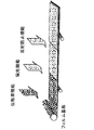


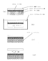


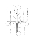


Classifications
-
- G—PHYSICS
- G02—OPTICS
- G02F—OPTICAL DEVICES OR ARRANGEMENTS FOR THE CONTROL OF LIGHT BY MODIFICATION OF THE OPTICAL PROPERTIES OF THE MEDIA OF THE ELEMENTS INVOLVED THEREIN; NON-LINEAR OPTICS; FREQUENCY-CHANGING OF LIGHT; OPTICAL LOGIC ELEMENTS; OPTICAL ANALOGUE/DIGITAL CONVERTERS
- G02F1/00—Devices or arrangements for the control of the intensity, colour, phase, polarisation or direction of light arriving from an independent light source, e.g. switching, gating or modulating; Non-linear optics
- G02F1/01—Devices or arrangements for the control of the intensity, colour, phase, polarisation or direction of light arriving from an independent light source, e.g. switching, gating or modulating; Non-linear optics for the control of the intensity, phase, polarisation or colour
- G02F1/13—Devices or arrangements for the control of the intensity, colour, phase, polarisation or direction of light arriving from an independent light source, e.g. switching, gating or modulating; Non-linear optics for the control of the intensity, phase, polarisation or colour based on liquid crystals, e.g. single liquid crystal display cells
- G02F1/133—Constructional arrangements; Operation of liquid crystal cells; Circuit arrangements
- G02F1/1333—Constructional arrangements; Manufacturing methods
-
- C—CHEMISTRY; METALLURGY
- C09—DYES; PAINTS; POLISHES; NATURAL RESINS; ADHESIVES; COMPOSITIONS NOT OTHERWISE PROVIDED FOR; APPLICATIONS OF MATERIALS NOT OTHERWISE PROVIDED FOR
- C09K—MATERIALS FOR MISCELLANEOUS APPLICATIONS, NOT PROVIDED FOR ELSEWHERE
- C09K19/00—Liquid crystal materials
- C09K19/04—Liquid crystal materials characterised by the chemical structure of the liquid crystal components, e.g. by a specific unit
- C09K19/38—Polymers
- C09K19/3833—Polymers with mesogenic groups in the side chain
- C09K19/3842—Polyvinyl derivatives
- C09K19/3852—Poly(meth)acrylate derivatives
-
- C—CHEMISTRY; METALLURGY
- C08—ORGANIC MACROMOLECULAR COMPOUNDS; THEIR PREPARATION OR CHEMICAL WORKING-UP; COMPOSITIONS BASED THEREON
- C08J—WORKING-UP; GENERAL PROCESSES OF COMPOUNDING; AFTER-TREATMENT NOT COVERED BY SUBCLASSES C08B, C08C, C08F, C08G or C08H
- C08J5/00—Manufacture of articles or shaped materials containing macromolecular substances
- C08J5/18—Manufacture of films or sheets
-
- C—CHEMISTRY; METALLURGY
- C09—DYES; PAINTS; POLISHES; NATURAL RESINS; ADHESIVES; COMPOSITIONS NOT OTHERWISE PROVIDED FOR; APPLICATIONS OF MATERIALS NOT OTHERWISE PROVIDED FOR
- C09K—MATERIALS FOR MISCELLANEOUS APPLICATIONS, NOT PROVIDED FOR ELSEWHERE
- C09K19/00—Liquid crystal materials
- C09K19/04—Liquid crystal materials characterised by the chemical structure of the liquid crystal components, e.g. by a specific unit
- C09K19/38—Polymers
- C09K19/3833—Polymers with mesogenic groups in the side chain
- C09K19/3842—Polyvinyl derivatives
- C09K19/3852—Poly(meth)acrylate derivatives
- C09K19/3861—Poly(meth)acrylate derivatives containing condensed ring systems
-
- G—PHYSICS
- G02—OPTICS
- G02F—OPTICAL DEVICES OR ARRANGEMENTS FOR THE CONTROL OF LIGHT BY MODIFICATION OF THE OPTICAL PROPERTIES OF THE MEDIA OF THE ELEMENTS INVOLVED THEREIN; NON-LINEAR OPTICS; FREQUENCY-CHANGING OF LIGHT; OPTICAL LOGIC ELEMENTS; OPTICAL ANALOGUE/DIGITAL CONVERTERS
- G02F1/00—Devices or arrangements for the control of the intensity, colour, phase, polarisation or direction of light arriving from an independent light source, e.g. switching, gating or modulating; Non-linear optics
- G02F1/01—Devices or arrangements for the control of the intensity, colour, phase, polarisation or direction of light arriving from an independent light source, e.g. switching, gating or modulating; Non-linear optics for the control of the intensity, phase, polarisation or colour
- G02F1/13—Devices or arrangements for the control of the intensity, colour, phase, polarisation or direction of light arriving from an independent light source, e.g. switching, gating or modulating; Non-linear optics for the control of the intensity, phase, polarisation or colour based on liquid crystals, e.g. single liquid crystal display cells
- G02F1/133—Constructional arrangements; Operation of liquid crystal cells; Circuit arrangements
- G02F1/1333—Constructional arrangements; Manufacturing methods
- G02F1/133305—Flexible substrates, e.g. plastics, organic film
-
- H—ELECTRICITY
- H05—ELECTRIC TECHNIQUES NOT OTHERWISE PROVIDED FOR
- H05B—ELECTRIC HEATING; ELECTRIC LIGHT SOURCES NOT OTHERWISE PROVIDED FOR; CIRCUIT ARRANGEMENTS FOR ELECTRIC LIGHT SOURCES, IN GENERAL
- H05B33/00—Electroluminescent light sources
- H05B33/12—Light sources with substantially two-dimensional radiating surfaces
-
- C—CHEMISTRY; METALLURGY
- C08—ORGANIC MACROMOLECULAR COMPOUNDS; THEIR PREPARATION OR CHEMICAL WORKING-UP; COMPOSITIONS BASED THEREON
- C08J—WORKING-UP; GENERAL PROCESSES OF COMPOUNDING; AFTER-TREATMENT NOT COVERED BY SUBCLASSES C08B, C08C, C08F, C08G or C08H
- C08J2323/00—Characterised by the use of homopolymers or copolymers of unsaturated aliphatic hydrocarbons having only one carbon-to-carbon double bond; Derivatives of such polymers
- C08J2323/02—Characterised by the use of homopolymers or copolymers of unsaturated aliphatic hydrocarbons having only one carbon-to-carbon double bond; Derivatives of such polymers not modified by chemical after treatment
-
- C—CHEMISTRY; METALLURGY
- C08—ORGANIC MACROMOLECULAR COMPOUNDS; THEIR PREPARATION OR CHEMICAL WORKING-UP; COMPOSITIONS BASED THEREON
- C08J—WORKING-UP; GENERAL PROCESSES OF COMPOUNDING; AFTER-TREATMENT NOT COVERED BY SUBCLASSES C08B, C08C, C08F, C08G or C08H
- C08J2345/00—Characterised by the use of homopolymers or copolymers of compounds having no unsaturated aliphatic radicals in side chain, and having one or more carbon-to-carbon double bonds in a carbocyclic or in a heterocyclic ring system; Derivatives of such polymers
-
- C—CHEMISTRY; METALLURGY
- C08—ORGANIC MACROMOLECULAR COMPOUNDS; THEIR PREPARATION OR CHEMICAL WORKING-UP; COMPOSITIONS BASED THEREON
- C08K—Use of inorganic or non-macromolecular organic substances as compounding ingredients
- C08K3/00—Use of inorganic substances as compounding ingredients
- C08K3/18—Oxygen-containing compounds, e.g. metal carbonyls
- C08K3/20—Oxides; Hydroxides
- C08K3/22—Oxides; Hydroxides of metals
-
- G—PHYSICS
- G02—OPTICS
- G02F—OPTICAL DEVICES OR ARRANGEMENTS FOR THE CONTROL OF LIGHT BY MODIFICATION OF THE OPTICAL PROPERTIES OF THE MEDIA OF THE ELEMENTS INVOLVED THEREIN; NON-LINEAR OPTICS; FREQUENCY-CHANGING OF LIGHT; OPTICAL LOGIC ELEMENTS; OPTICAL ANALOGUE/DIGITAL CONVERTERS
- G02F1/00—Devices or arrangements for the control of the intensity, colour, phase, polarisation or direction of light arriving from an independent light source, e.g. switching, gating or modulating; Non-linear optics
- G02F1/01—Devices or arrangements for the control of the intensity, colour, phase, polarisation or direction of light arriving from an independent light source, e.g. switching, gating or modulating; Non-linear optics for the control of the intensity, phase, polarisation or colour
- G02F1/13—Devices or arrangements for the control of the intensity, colour, phase, polarisation or direction of light arriving from an independent light source, e.g. switching, gating or modulating; Non-linear optics for the control of the intensity, phase, polarisation or colour based on liquid crystals, e.g. single liquid crystal display cells
- G02F1/133—Constructional arrangements; Operation of liquid crystal cells; Circuit arrangements
- G02F1/1333—Constructional arrangements; Manufacturing methods
- G02F1/1335—Structural association of cells with optical devices, e.g. polarisers or reflectors
- G02F1/133509—Filters, e.g. light shielding masks
- G02F1/133514—Colour filters
- G02F1/133516—Methods for their manufacture, e.g. printing, electro-deposition or photolithography
-
- Y—GENERAL TAGGING OF NEW TECHNOLOGICAL DEVELOPMENTS; GENERAL TAGGING OF CROSS-SECTIONAL TECHNOLOGIES SPANNING OVER SEVERAL SECTIONS OF THE IPC; TECHNICAL SUBJECTS COVERED BY FORMER USPC CROSS-REFERENCE ART COLLECTIONS [XRACs] AND DIGESTS
- Y02—TECHNOLOGIES OR APPLICATIONS FOR MITIGATION OR ADAPTATION AGAINST CLIMATE CHANGE
- Y02P—CLIMATE CHANGE MITIGATION TECHNOLOGIES IN THE PRODUCTION OR PROCESSING OF GOODS
- Y02P20/00—Technologies relating to chemical industry
- Y02P20/50—Improvements relating to the production of bulk chemicals
- Y02P20/582—Recycling of unreacted starting or intermediate materials
Landscapes
- Chemical & Material Sciences (AREA)
- Physics & Mathematics (AREA)
- Engineering & Computer Science (AREA)
- Crystallography & Structural Chemistry (AREA)
- Materials Engineering (AREA)
- Organic Chemistry (AREA)
- Nonlinear Science (AREA)
- Manufacturing & Machinery (AREA)
- General Physics & Mathematics (AREA)
- Optics & Photonics (AREA)
- Mathematical Physics (AREA)
- Health & Medical Sciences (AREA)
- Chemical Kinetics & Catalysis (AREA)
- Medicinal Chemistry (AREA)
- Polymers & Plastics (AREA)
- Electroluminescent Light Sources (AREA)
- Liquid Crystal (AREA)
- Laminated Bodies (AREA)
- Polarising Elements (AREA)
Description
本発明は、液晶パネル用ベースフィルム、液晶パネル用ベールフィルムを用いた機能フィルム、機能フィルムを用いた液晶パネルおよび、裏面光源、液晶パネルおよび、裏面光源を搭載した電子機器、機能フィルムの製造方法、機能フィルムの製造装置および液晶パネル用ベースフィルムの製造装置に関する。 The present invention relates to a base film for a liquid crystal panel, a functional film using a bale film for a liquid crystal panel, a liquid crystal panel using the functional film, a back light source, a liquid crystal panel, an electronic device equipped with the back light source, and a method for producing the functional film The present invention relates to a functional film manufacturing apparatus and a liquid crystal panel base film manufacturing apparatus.
近年の情報化社会の進展により、画像装置は、室内の据え置き型は大画面化が要求され、携帯型はさまざまな場所で使われるために、暗所・明所のいずれでも使用できることが必須である。更に、据え置き型・携帯型共に軽量化が要求されている。この結果として、従来から使われていたCRT(Cathode Ray Tube)ディスプレイは、平面ディスプレイに置き換わりつつある。 Due to the progress of the information society in recent years, it is indispensable that the imaging device can be used in both dark and light places because the indoor stationary type is required to have a large screen and the portable type is used in various places. is there. Furthermore, weight reduction is required for both stationary and portable types. As a result, a CRT (Cathode Ray Tube) display that has been conventionally used is being replaced by a flat display.
情報機器も、室内の据え置き型から携帯型としての用途が拡大している。据え置き型と異なり、携帯型の情報機器はさまざまな場所で使われる。据え置き型は、大画面化・高輝度化・視野角の広さが要求され、携帯型は、使用される場所が多岐にわたるために、暗い場所から明るい場所までの画像の視認性と落下等の耐衝撃性の向上が求められている。 The use of information devices from indoor stationary types to portable types is also expanding. Unlike the stationary type, portable information devices are used in various places. The stationary type is required to have a large screen, high brightness, and wide viewing angle, and the portable type is used for a wide variety of places, so the visibility of images from dark places to bright places and dropping etc. There is a need for improved impact resistance.
平面型のディスプレイは、プラズマディスプレイ(Plasma Display Panel)、液晶ディスプレイ(Liquid Crystal Display)と有機ELディスプレイ(Organic Light Emitted Display)が知られている。プラズマディスプレイは動作原理から高電圧を発生させる必要があり携帯には不向きで、低消費電力で駆動可能な液晶ディスプレイと有機ELディスプレイとが携帯用として向いている。 As the flat type display, a plasma display (Plasma Display Panel), a liquid crystal display (Liquid Crystal Display), and an organic EL display (Organic Light Emitted Display) are known. A plasma display needs to generate a high voltage because of its operating principle and is not suitable for carrying. A liquid crystal display and an organic EL display that can be driven with low power consumption are suitable for carrying.
高輝度・視野角の広さから、大型化のディスプレイとしては、プラズマディスプレイが先行したが、液晶ディスプレイは軽量化が可能であり、大型化もプラズマディスプレイと同様に可能であるために最近ではプラズマディスプレイ同様に大型化も行われている。 Plasma display has been the leading display for large display due to its high brightness and wide viewing angle. However, liquid crystal displays can be reduced in weight and increased in size in the same way as plasma displays. The size of the display is increasing.
一方、携帯型として、プラズマディスプレイは動作原理から高電圧を発生させる必要があり携帯には不向きで、低消費電力で駆動可能な液晶ディスプレイと有機ELディスプレイとが携帯用として向いている。 On the other hand, as a portable type, a plasma display needs to generate a high voltage from the operation principle and is not suitable for carrying, and a liquid crystal display and an organic EL display that can be driven with low power consumption are suitable for portable use.
現状では液晶ディスプレイが主流であるが、有機ELディスプレイは画像の鮮明さで今後伸びてくることが予想されている。 At present, liquid crystal displays are the mainstream, but organic EL displays are expected to grow in the future due to the sharpness of images.
有機ELディスプレイと液晶ディスプレイとは、個々の画素にアクティブ素子を備えて画素を駆動する「アクティブ駆動型」と、2組の直交する短冊状の電極群により画素を駆動する「単純マトリクス型」がある。アクティブ駆動型は、単純マトリクス型に比べ、応答時間を飛躍的に短くでき、多数の画素の動画表示が可能となる。更に、コントラストや階調など画質に関連する制御をきめ細かく行うことができるようになり、CRT並みの動画表示を可能とするものである。この結果、「アクティブ駆動型」が現在の駆動方式の主流となっている。 The organic EL display and the liquid crystal display are divided into an “active drive type” in which each pixel is provided with an active element to drive the pixel, and a “simple matrix type” in which the pixel is driven by two sets of orthogonal strip electrode groups. is there. The active drive type can drastically shorten the response time compared to the simple matrix type, and can display a moving image of a large number of pixels. Furthermore, the control related to the image quality such as the contrast and the gradation can be finely performed, and the moving image display similar to the CRT can be performed. As a result, the “active drive type” has become the mainstream of the current drive system.
CRT、有機ELディスプレイは自発光型であるのに対し、液晶ディスプレイは、透過光、あるいは反射光を用いることで発色を得るものである。液晶ディスプレイは、画素電極が光を透過するか、反射するか、一部を透過して一部を反射するか、により、それぞれ透過型、反射型、半透過型の3種類に分類される。 While CRT and organic EL displays are self-luminous type, liquid crystal displays obtain color by using transmitted light or reflected light. Liquid crystal displays are classified into three types, a transmissive type, a reflective type, and a semi-transmissive type, depending on whether the pixel electrode transmits light, reflects light, or partially transmits light and partially reflects light.
据え置き型のように、使用場所が室内に限定されている場合、透過型液晶ディスプレイや有機ELディスプレイは画像が鮮明である。しかし、自発光の発光強度よりも明るい屋外では画像のコントラストが下がり、画像が見えにくいという欠点がある。屋外でもコントラストが下がらないように発光源の強度を上げると、屋内の画質にギラツキが生じる、消費電力が大きくなるという問題が発生する。 When the place of use is limited to a room as in the stationary type, the transmissive liquid crystal display or the organic EL display has a clear image. However, there is a drawback in that the contrast of the image is lowered and the image is difficult to see outdoors when it is brighter than the light emission intensity of the self-light emission. If the intensity of the light emitting source is increased so that the contrast does not decrease even outdoors, there are problems that glare is produced in the indoor image quality and power consumption is increased.
これに対し、反射型の液晶ディスプレイは、外光を反射して画像を表示するので屋外での視認性に優れるが、暗い場所では画像が見えにくいという欠点がある。フロントライトを設けることで改善できるが、フロントライトの場合、携帯型のように小画面の場合でも、画面全体を一様に照射することが難しいという欠点がある。 On the other hand, a reflective liquid crystal display is excellent in visibility outdoors because it reflects external light and displays an image, but has a drawback that it is difficult to see an image in a dark place. This can be improved by providing a front light, but the front light has a drawback that it is difficult to uniformly irradiate the entire screen even in the case of a small screen such as a portable type.
透過型と反射型の長所を備えた液晶ディスプレイとして半透過型液晶ディスプレイがある。半透過型液晶ディスプレイは、画素電極を半透過にしたり開口を設けたりすることによりバックライトの光と外光との両方を表示に利用するため、屋外と室内の両方で視認性が確保できる。このため現在の携帯用情報端末はほとんど半透過型液晶パネルが使われている。 There is a transflective liquid crystal display as a liquid crystal display having advantages of a transmissive type and a reflective type. Since the transflective liquid crystal display uses both backlight light and external light for display by making the pixel electrode translucent or providing an opening, visibility can be ensured both outdoors and indoors. For this reason, most current portable information terminals use transflective liquid crystal panels.
しかしながら、半透過型液晶ディスプレイの画像は、暗い場所では透過型液晶ディスプレイや有機ELディスプレイに劣り、明るい場所では反射型液晶ディスプレイに劣る。このために、携帯情報端末として更なる画質の向上を図る必要がある。 However, the image of the transflective liquid crystal display is inferior to the transmissive liquid crystal display and the organic EL display in a dark place, and inferior to the reflective liquid crystal display in a bright place. For this reason, it is necessary to further improve image quality as a portable information terminal.
さらに、ディスプレイは、情報端末、例えば、携帯電話やPDA(Personal Digital Assistant、パーソナル・デジタル・アシ スタント)等のモバイル機器や、デジタルカメラ、デジタルビディオカメラ等があり、個人用途から業務用途まで幅広く使われ、使われる場所もさまざまであり、表示装置の堅牢さも必要とされている。 In addition, displays include information terminals, for example, mobile devices such as mobile phones and PDAs (Personal Digital Assistants), digital cameras, and digital video cameras. However, the place where it is used varies, and the robustness of the display device is also required.
携帯用としてディスプレイパネルに要求される特性は、上記の画質以外に、画面サイズ、パネルの薄さ、消費電力等がある。 In addition to the above image quality, the characteristics required of a display panel for portable use include screen size, panel thinness, power consumption, and the like.
堅牢性はパネルの厚さを薄くする、更に、基板を対衝撃に対し割れない基板を用いる必要がある。パネルの厚さに関しては、有機ELディスプレイは原理的に基板1枚の厚さまで薄型化が可能である。これに対し、液晶ディスプレイパネルは、反射型液晶ディスプレイは基板2枚の厚さまで薄型化が可能であるが、透過型/半透過型液晶ディスプレイはバックライトが必要なため厚くならざるを得ない。 For robustness, it is necessary to reduce the thickness of the panel and to use a substrate that does not break the substrate against impact. Regarding the thickness of the panel, the organic EL display can be reduced to the thickness of one substrate in principle. On the other hand, in the liquid crystal display panel, the reflective liquid crystal display can be thinned to the thickness of two substrates, but the transmissive / semi-transmissive liquid crystal display must be thick because a backlight is required.
画質以外の、外形寸法、重さ、壊れ難さ、消費電力、価格等について考察する。外形寸法と重さは、バックライト等の光源が不要な有機ELディスプレイが圧倒的に有利である。有効な封止技術により、原理的にはほぼ支持基板1枚の厚さまで薄型化、軽量化できる。補助光源を搭載しなければ反射型液晶ディスプレイパネルの厚さと重さは、ほぼ支持基板2枚分になるが、それでも有機ELディスプレイに比べて不利である。 In addition to image quality, we will consider external dimensions, weight, difficulty of breaking, power consumption, price, etc. In terms of external dimensions and weight, organic EL displays that do not require a light source such as a backlight are overwhelmingly advantageous. With effective sealing technology, in principle, the thickness can be reduced to a thickness of almost one supporting substrate. Without the auxiliary light source, the thickness and weight of the reflective liquid crystal display panel is approximately the same as that of the two support substrates, but it is still disadvantageous compared to the organic EL display.
壊れ難さについては同じ基板を用いる限り大差は無い。消費電力については反射型液晶ディスプレイが有利だが、補助光源を搭載すれば透過型液晶ディスプレイや有機ELディスプレイと同等である。 As long as the same substrate is used, there is not much difference in the difficulty of breaking. A reflective liquid crystal display is advantageous in terms of power consumption, but if an auxiliary light source is installed, it is equivalent to a transmissive liquid crystal display or an organic EL display.
一方、半透過型液晶ディスプレイの場合は、明るい場所ではバックライトを消灯して消費電力を低減できる。更に、液晶ディスプレイは有機ELディスプレイに比べて長年の製品化の歴史があり、価格で有利と考えられる。 On the other hand, in the case of a transflective liquid crystal display, power consumption can be reduced by turning off the backlight in a bright place. Furthermore, liquid crystal displays have a long history of commercialization compared to organic EL displays, and are considered advantageous in price.
最高性能の液晶ディスプレイは既に人が認知できる精細度や色数の上限にほぼ到達しており、これ以上の画質の向上は大きな意味を持たない。従って、現在の研究活動は画質以外の性能の向上にも重点が置かれている。 The highest-performance liquid crystal display has already reached the upper limit of the definition and the number of colors that can be recognized by humans, and further improvements in image quality are not significant. Therefore, current research activities focus on improving performance other than image quality.
例えば、低温多結晶シリコン薄膜トランジスタ(poly−Si TFT)技術により、従来は外付けしていた電子回路をガラス基板上に集積できる。これにより、液晶ディスプレイの部品点数の削減、狭額縁化、消費電力の低減が既に進展している。また、従来のガラス基板をプラスチック基板で代替した液晶ディスプレイの研究は、薄型化、軽量化、落としても壊れないタフさを追求したものである。 For example, by using a low-temperature polycrystalline silicon thin film transistor (poly-Si TFT) technology, an electronic circuit that has been conventionally attached can be integrated on a glass substrate. As a result, the reduction of the number of parts of the liquid crystal display, the narrowing of the frame, and the reduction of the power consumption have already progressed. In addition, research on liquid crystal displays in which conventional glass substrates are replaced with plastic substrates has been pursued to be thinner, lighter, and tough without breaking.
一方、 有機ELディスプレイは、薄型、軽量、暗所での優れた視認性において液晶ディスプレイを凌ぐ可能性を備えており、発光効率と寿命の改善が研究されている。 On the other hand, organic EL displays have the potential to surpass liquid crystal displays in terms of thinness, light weight, and excellent visibility in the dark, and studies have been made on improving luminous efficiency and lifetime.
以上に説明したように、据え置き用途には、プラズマディスプレイ、透過型液晶ディスプレイ、有機ELディスプレイが、携帯用途には、半透過型液晶ディスプレイが適している。 As described above, plasma displays, transmissive liquid crystal displays, and organic EL displays are suitable for stationary applications, and transflective liquid crystal displays are suitable for portable applications.
据え置き用と携帯用との両方の用途に向く点で、液晶ディスプレイは、プラズマディスプレイや有機ELディスプレイにはない長所を備えたディスプレイであるがことが分かる。 It can be seen that the liquid crystal display is a display having advantages not found in the plasma display or the organic EL display in that it is suitable for both stationary use and portable use.
図27に従来の半透過型液晶ディスプレイパネルの断面図を示す。液晶パネルは、図27の上半分に示すように、液晶を2枚の基板で挟んで構成される。一方のガラス基板312の片側には、薄膜トランジスタ311と画素電極310とを備えた画素が規則正しく配列され、薄膜トランジスタ311を駆動するための電気信号を送るために配線も形成されている。ここで画素電極310は、透過率が30〜70%で設計される。通常は、透過率70%で設計されることが多い。 FIG. 27 shows a sectional view of a conventional transflective liquid crystal display panel. As shown in the upper half of FIG. 27, the liquid crystal panel is configured by sandwiching liquid crystal between two substrates. On one side of one glass substrate 312, pixels each provided with a thin film transistor 311 and a pixel electrode 310 are regularly arranged, and wiring is also formed to send an electric signal for driving the thin film transistor 311. Here, the pixel electrode 310 is designed with a transmittance of 30 to 70%. Usually, it is often designed with a transmittance of 70%.
もう一方のガラス基板304の片側には、カラーフィルタ305が配置される。カラーフィルタ(CF)305は画素電極、ブラックマトリクス(BM)は画素電極間の境界に対向する位置にそれぞれ配置され、透明電極307がこれらを覆っている。これら2枚の基板の表面には、液晶を所望の方向へ配向させるための配向膜307、309が各々形成されている。また、これら2枚の基板は、基板の周辺部に配置されたシール材Bにより固定され、液晶はこれら2枚の基板の隙間に封入されている。
A
このような液晶を挟んだ2枚の基板の外側には、様々な光学機能を持つフィルム基板が貼り合わせられる。ここでは、偏光板(直線偏光板)302、314と位相差膜(1/4波長板)303、313との2枚のフィルム基板を積層して、入射光を円偏光にする機能を持たせている。更に、外光の反射を防ぐための反射防止板301も設けられる。 A film substrate having various optical functions is bonded to the outside of the two substrates sandwiching the liquid crystal. Here, two film substrates of polarizing plates (linear polarizing plates) 302 and 314 and retardation films (quarter-wave plates) 303 and 313 are laminated so as to have a function of converting incident light into circularly polarized light. ing. Furthermore, an antireflection plate 301 for preventing reflection of external light is also provided.
シール材Bを塗布するときには、後の液晶注入のための開口部を残しておく。またここで2枚の基板の隙間を一定に保つために、予め隙間の距離(例えば6μm程度)に対応したスペーサを散布しておく。スペーサの大きさは画素電極よりもかなり小さい。これを一定の荷重の下で焼成した後に、シール材の開口部から液晶を注入し、最後に紫外線硬化材料でシール材の開口部を封止して液晶パネルが完成する。 When the sealing material B is applied, an opening for subsequent liquid crystal injection is left. Here, in order to keep the gap between the two substrates constant, spacers corresponding to the gap distance (for example, about 6 μm) are sprayed in advance. The size of the spacer is considerably smaller than the pixel electrode. After firing this under a certain load, liquid crystal is injected from the opening of the sealing material, and finally the opening of the sealing material is sealed with an ultraviolet curable material to complete the liquid crystal panel.
図27の下半分にはバックライトの構成が示されている。 The lower half of FIG. 27 shows the configuration of the backlight.
バックライトは、白色光を出力する、ランプや発光ダイオード(LED))等の光源C、導光体317、反射板318、拡散シート316および、視野角調整シート315と、からなっている。 The backlight includes a light source C such as a lamp or a light emitting diode (LED) that outputs white light, a light guide 317, a reflection plate 318, a diffusion sheet 316, and a viewing angle adjustment sheet 315.
ここで、バックライトができるだけ一様な面発光体として動作するように、また、光源Cが発する光をできるだけ効率良く液晶パネルの方向へ導くように、これらの構成要素の設計が最適化されている。通常、導光体としてはポリメチルメタクリレート(PMMA)などの透明のプラスチック基板が用いられ、厚さは1.0mm程度である。反射板318、拡散シート316、視野角調整シート315は、各々の光学機能を果たすための加工を施したもので、図27のバックライトの構成要素を全て加えると厚さは2.0mm程度になる。 Here, the design of these components is optimized so that the backlight operates as a uniform surface light emitter as much as possible, and the light emitted from the light source C is guided as efficiently as possible toward the liquid crystal panel. Yes. Usually, a transparent plastic substrate such as polymethyl methacrylate (PMMA) is used as the light guide, and the thickness is about 1.0 mm. The reflection plate 318, the diffusion sheet 316, and the viewing angle adjustment sheet 315 are processed to perform their respective optical functions, and when all the components of the backlight in FIG. Become.
次に、図27を参照しながら半透過型液晶ディスプレイの、透過型液晶ディスプレイとしての動作を説明する。 Next, the operation of the transflective liquid crystal display as a transmissive liquid crystal display will be described with reference to FIG.
光源Cから発せられた白色光は導光体317に入射し、反射板318によって進路を変えられて拡散シート316で拡散される。拡散光は視野角調整シート315によって所望の指向性を持つように調整されたのちに液晶パネルに到る。この光は無偏光の状態だが、ある一方の直線偏光のみが液晶パネルの直線偏光板314を透過する。この直線偏光は位相差板(1/4波長板)313によって円偏光になり、ガラス基板312、半透明な材料で形成された画素電極310、等を順次透過して液晶層308に到る。 The white light emitted from the light source C is incident on the light guide 317, the route is changed by the reflection plate 318, and is diffused by the diffusion sheet 316. The diffused light is adjusted to have a desired directivity by the viewing angle adjusting sheet 315 and then reaches the liquid crystal panel. Although this light is unpolarized, only one linearly polarized light passes through the linear polarizing plate 314 of the liquid crystal panel. This linearly polarized light becomes circularly polarized light by the phase difference plate (¼ wavelength plate) 313, and sequentially passes through the glass substrate 312, the pixel electrode 310 formed of a translucent material, and the like to reach the liquid crystal layer 308.
ここで画素電極310と対向する透明な電極(対向電極)306との間の電位差の有無により、液晶分子の配向状態が制御されている。即ち、ある極端な配向状態においては、図27の下方から入射した円偏光がそのままの状態で液晶層308、透明電極306を透過し、ある特定の波長範囲の光がカラーフィルタ305を透過して位相差板(1/4波長板)313に到り、偏光板(直線偏光板)314をほぼ完全に透過する。従って、この画素はカラーフィルタで決まる色を最も明るく表示する。
Here, the alignment state of the liquid crystal molecules is controlled by the presence or absence of a potential difference between the transparent electrode (counter electrode) 306 facing the pixel electrode 310. That is, in an extreme alignment state, the circularly polarized light incident from the lower side of FIG. 27 is transmitted through the liquid crystal layer 308 and the transparent electrode 306, and light in a specific wavelength range is transmitted through the
また、別の極端な配向状態においては逆に、液晶層を通過する光の偏光状態が変化して、カラーフィルタを透過した光を位相差板(1/4波長板)303と偏光板(直線偏光板)302とがほぼ完全に吸収する。従って、この画素は黒を表示する。これら2つの状態の中間の配向状態では光が部分的に透過するため、この画素は中間色を表示することになる。 On the other hand, in another extreme alignment state, the polarization state of the light passing through the liquid crystal layer changes, and the light transmitted through the color filter is changed into a retardation plate (¼ wavelength plate) 303 and a polarizing plate (straight line). (Polarizing plate) 302 absorbs almost completely. Therefore, this pixel displays black. In the intermediate alignment state between these two states, light is partially transmitted, so this pixel displays an intermediate color.
次に、半透過型液晶ディスプレイの反射型液晶ディスプレイとしての動作を説明する。 Next, the operation of the transflective liquid crystal display as a reflective liquid crystal display will be described.
外光が図27の上方から液晶パネルに入射した場合には、偏光板(直線偏光板)302と位相差板(1/4波長板)303を透過した円偏光が液晶層を通過し、画素電極によってその30%が反射されて表示に利用される。従って、反射型液晶ディスプレイとして動作する。 When external light is incident on the liquid crystal panel from above in FIG. 27, the circularly polarized light transmitted through the polarizing plate (linear polarizing plate) 302 and the retardation plate (¼ wavelength plate) 303 passes through the liquid crystal layer, and the pixel 30% of the light is reflected by the electrodes and used for display. Therefore, it operates as a reflective liquid crystal display.
次に、半透過型液晶ディスプレイの動作を説明する。 Next, the operation of the transflective liquid crystal display will be described.
半透過型液晶ディスプレイの場合は、画素電極は半透明な材料で形成されており、透過型液晶ディスプレイとしての動作はほぼ前述の通りである。但し、画素電極の光の透過率を例えば70%に設計した場合には、30%の光が表示に用いられないことになる。一方、外光が図27の上方から液晶パネルに入射した場合には、直線偏光板と1/4波長板を透過した円偏光が液晶層を通過し、画素電極によってその30%が反射されて表示に利用される。従って、反射型液晶ディスプレイとして動作する。 In the case of a transflective liquid crystal display, the pixel electrode is formed of a translucent material, and the operation as a transmissive liquid crystal display is almost as described above. However, when the light transmittance of the pixel electrode is designed to be 70%, for example, 30% of the light is not used for display. On the other hand, when external light is incident on the liquid crystal panel from above in FIG. 27, circularly polarized light that has passed through the linearly polarizing plate and the quarter-wave plate passes through the liquid crystal layer, and 30% is reflected by the pixel electrode. Used for display. Therefore, it operates as a reflective liquid crystal display.
従来は、薄膜トランジスタを形成する基板は、薄膜トランジスタを製造する際の高温に耐えるようにガラス基板が用いられている。一方、より低温で薄膜トランジスタを形成する技術も研究されているが、近年の小型化に伴い、機能素子も液晶を駆動する薄膜トランジスタと同じ基板形成するためには素子特性に問題があり実用化されてはいない。 Conventionally, a glass substrate is used as a substrate on which a thin film transistor is formed so as to withstand high temperatures when the thin film transistor is manufactured. On the other hand, technology for forming a thin film transistor at a lower temperature has also been studied. However, with the recent downsizing, functional elements have a problem in element characteristics and are put into practical use in order to form the same substrate as a thin film transistor that drives liquid crystal. No.
薄膜トランジスタは、石英基板上に形成する高温ポリシリコントランジスタ・ガラス基板上に形成する低温ポリシリコントランジスタ・ガラス基板またはプラスチック基板上に形成するアモルファスシリコントランジスタの3種類がある。液晶パネルの小型化のため、従来外付けであったドライバICをガラス基板上に形成する事が行われている。アモルファスシリコントランジスタは最も低温で製造が可能であるが、ドライバICを動作するだけの特性をプラスチック基板上で実用化することはできていない。このために、現状の製造技術では低温ポリシリコントランジスタをガラス基板上に形成することが現実的である。 There are three types of thin film transistors: a high-temperature polysilicon transistor formed on a quartz substrate, a low-temperature polysilicon transistor formed on a glass substrate, a glass substrate, or an amorphous silicon transistor formed on a plastic substrate. In order to reduce the size of the liquid crystal panel, a driver IC, which has been conventionally externally attached, is formed on a glass substrate. Amorphous silicon transistors can be manufactured at the lowest temperature, but characteristics sufficient to operate a driver IC cannot be put to practical use on a plastic substrate. For this reason, it is practical to form a low-temperature polysilicon transistor on a glass substrate with the current manufacturing technology.
図28に示すように、プラスチック基板を用いた透過型液晶ディスプレイは、例えばAsanoらの論文(A. Asano and T. Kinoshita、 “Low−temperature polycrystalline−Silicon TFT color LCD panel made of plastic substrates、” in Society for Information Display International Symposium Digest of Technical Papers (Society for Information Display、 Boston、 2002、) Vol. 33、 pp. 1196−1199.)に見るように試作されている。 As shown in FIG. 28, a transmissive liquid crystal display using a plastic substrate is disclosed in, for example, an article by Asano et al. (A. Asano and T. Kinoshita, “Low-temperature polycrystallin-Silicon TFT color LCD panel made plastic” Society for Information Display International Symposium Digest of Technical Papers (Society for Information Display, Boston, 2002,) Vol.33, p.
上記論文では、エッチング阻止層を設けたガラス基板上に、既知の低温多結晶シリコン薄膜トランジスタの製造方法によりポリシリコンTFTを形成し、ポリシリコンTFT上に取り外し可能な接着剤を形成し、仮基板を貼り付ける(図28(a))。次に、フッ酸(HF)によりガラス基板をエッチング除去する(図28(b))。その後、エッチング阻止層を除去後、接着剤を介して厚さ0.2mmのプラスチック基板にポリシリコンTFTを接着させる(図28(c))。その後、仮基板を除去し、次に、取り外し可能な接着剤を除去する(図28(d))。その後、該基板と、カラーフィルタ・透明電極等が形成され基板と対向させ間隙に液晶分子を注入することでアクティブ駆動液晶表示パネルを形成する。 In the above paper, a polysilicon TFT is formed on a glass substrate provided with an etching stopper layer by a known low-temperature polycrystalline silicon thin film transistor manufacturing method, a removable adhesive is formed on the polysilicon TFT, and a temporary substrate is formed. Affix (FIG. 28A). Next, the glass substrate is removed by etching with hydrofluoric acid (HF) (FIG. 28B). Thereafter, after removing the etching stopper layer, a polysilicon TFT is bonded to a plastic substrate having a thickness of 0.2 mm through an adhesive (FIG. 28C). Thereafter, the temporary substrate is removed, and then the removable adhesive is removed (FIG. 28D). Thereafter, an active drive liquid crystal display panel is formed by injecting liquid crystal molecules into the gap so that the substrate, a color filter, a transparent electrode, and the like are formed and face the substrate.
従来の透過型/半透過型液晶ディスプレイはバックライトを用いるために厚くなり、且つ、重くなる。この課題を解決する手法として,有機ELを用いる構成が提案されている。 Conventional transmissive / semi-transmissive liquid crystal displays are thicker and heavier due to the use of a backlight. As a technique for solving this problem, a configuration using an organic EL has been proposed.
有機ELをバックライトに使ったものが、特開2000―29034号公報や特開2002−98957に開示されている。以下、図29を用いて説明する。 Japanese Patent Application Laid-Open No. 2000-29034 and Japanese Patent Application Laid-Open No. 2002-98957 disclose the use of organic EL as a backlight. This will be described below with reference to FIG.
図29(a)に示される特開2000―29034号公報は、従来の焼成による配向膜の形成による有機ELの劣化防止のために、予め配向処理を施した配向膜623を表示駆動基板621及び対向基板622にラミネートすることで従来の焼成による配向膜を形成する際の高温による有機ELの劣化が防止される。 In Japanese Patent Laid-Open No. 2000-29034 shown in FIG. 29A, an alignment film 623 that has been subjected to an alignment process in advance is used to prevent deterioration of the organic EL due to the formation of an alignment film by conventional baking. By laminating the counter substrate 622, deterioration of the organic EL due to a high temperature when forming an alignment film by conventional baking is prevented.
図29(a)の液晶表示パネルは、予め別々の工程で製造されたTFTアレイ基板621と、面発光体を備えた対向基板622に、ポリマーフィルム をラミネートし、その後、通常のラビング処理を行うことに より、上記のポリマーフィルムに液晶組成物624に対する配向機能を付加し、配向膜623を形成する。その後、TFTアレイ基板621と対向基板622との配向膜623を対向させその間隙に液晶組成物624を充填したものである。 The liquid crystal display panel of FIG. 29A is obtained by laminating a polymer film on a TFT array substrate 621 manufactured in separate steps and a counter substrate 622 provided with a surface light emitter, and then performing a normal rubbing process. Accordingly, an alignment function with respect to the liquid crystal composition 624 is added to the polymer film, so that an alignment film 623 is formed. Thereafter, the alignment film 623 of the TFT array substrate 621 and the counter substrate 622 is opposed to each other, and a liquid crystal composition 624 is filled in the gap.
図29(a)の構造は、図27に示した従来技術の図における配向膜が有機フィルムをラミネートした点および、バックライトを有機ELに置き換えたもので、有機ELを形成するための基板は必要であるが、従来の導光板が数mmであるのに対し、ガラス基板が0.4mmであることから薄膜化が図られている。 The structure shown in FIG. 29A is obtained by laminating an organic film with the alignment film in the prior art diagram shown in FIG. 27, and replacing the backlight with an organic EL. A substrate for forming the organic EL is Although it is necessary, since the conventional light guide plate is several mm, the glass substrate is 0.4 mm, so that the thinning is achieved.
一方、特開2000―98957に、透過型の液晶パネルのバックライトを従来の蛍光管方式に変えて、有機EL発光素子を用いることで薄膜化・軽量化を図るものがある。図29(b)に構造を示す。 On the other hand, Japanese Patent Laid-Open No. 2000-98957 discloses a technique for reducing the thickness and weight by using an organic EL light-emitting element instead of a conventional fluorescent tube system for a transmissive liquid crystal panel backlight. FIG. 29B shows the structure.
液晶表示パネルは、第1電極基板650、第2電極基板660及びこれら基板間に保持された液晶層を備えている。 The liquid crystal display panel includes a first electrode substrate 650, a second electrode substrate 660, and a liquid crystal layer held between these substrates.
第1電極基板650は、透明なガラス基板651で構成されており、液晶層と接する側の表面には、走査線652、信号線653(図示せず)、画素電極654、TFT655、補助容量656(図示せず)、及び補助容量線657が形成されている。 The first electrode substrate 650 is formed of a transparent glass substrate 651, and has a scanning line 652, a signal line 653 (not shown), a pixel electrode 654, a TFT 655, and an auxiliary capacitor 656 on the surface in contact with the liquid crystal layer. (Not shown) and auxiliary capacitance lines 657 are formed.
第2電極基板680は、透明なガラス基板681上の液晶と接する面に液晶の対向電極となる透明電極682が形成され、ガラス基板681の基板透明電極682が形成されている面と対向する面には有機ELの発光部分683、685、687,689が形成され、発光部分683、685、687,689の間隙となる非発光部分684、686、688が形成されている。
The second electrode substrate 680 has a transparent electrode 682 serving as a counter electrode for liquid crystal formed on the surface of the transparent glass substrate 681 in contact with the liquid crystal, and a surface facing the surface of the glass substrate 681 on which the substrate transparent electrode 682 is formed. Are formed with light emitting
図29(b)は、液晶パネルの対向電極が形成された基板の裏面に有機ELからなる平面発光素子を形成することで、従来必要とされていたバックライト用の導光板を無くすことで薄膜化を達成するものである。この結果、基板を図29(a)の基板が3枚必要な構成に比べ、基板を2枚に減らすことが可能となり、液晶パネルの薄膜化が可能となる。 FIG. 29B shows a thin film by forming a planar light emitting element made of organic EL on the back surface of the substrate on which the counter electrode of the liquid crystal panel is formed, thereby eliminating the light guide plate for the backlight which has been conventionally required. Is achieved. As a result, it is possible to reduce the number of substrates to two as compared with the configuration that requires three substrates in FIG. 29A, and the liquid crystal panel can be made thinner.
一方、液晶パネルを構成する基板に長尺状のフレキシブルフィルムを用いる技術は特開昭54−126559号公報に開示されている。しかしながら同公報には、透明電極と配向膜が形成された長尺状のフレキシブルフィルムフィルムを用いて単純マトリックス駆動型の白黒液晶パネルを形成する例が示されているに過ぎない。特開昭54−126559号公報は、大型で平滑なガラス基板が高価であり、製造が困難であった時代に長尺のプラスチック基板を用いて液晶パネルを製造するものである。更に、特開昭62−150218号公報、特開平6−27448号公報には、2枚の電極上に配向膜が形成された長尺のフレキシブルフィルムの間隙に液晶を狭持する技術が開示されている。 On the other hand, a technique of using a long flexible film for a substrate constituting a liquid crystal panel is disclosed in Japanese Patent Laid-Open No. 54-126559. However, the publication only shows an example of forming a simple matrix drive type monochrome liquid crystal panel using a long flexible film film on which a transparent electrode and an alignment film are formed. Japanese Patent Application Laid-Open No. 54-126559 manufactures a liquid crystal panel using a long plastic substrate in a time when a large and smooth glass substrate is expensive and difficult to manufacture. Furthermore, Japanese Patent Application Laid-Open Nos. Sho 62-150218 and Hei 6-27448 disclose a technique for holding a liquid crystal in a gap between a long flexible film in which an alignment film is formed on two electrodes. ing.
しかしながら、液晶パネルのカラー化、動画を表示することが要求された。応答速度を高速化するため、駆動方式が液晶の画素を直接薄膜トランジスタで駆動するアクティブマトリックス駆動に切り替わった。更に、カラー表示のため、光学機能膜も、配向膜以外に位相差膜、偏光膜等が必要となる。また表示の視認性の向上も要求され透過型・反射型・半透過型の種々のタイプの液晶パネルが開発され、これらに対応できる技術は開示されていない。 However, colorization of liquid crystal panels and display of moving images have been required. In order to increase the response speed, the driving method has been switched to active matrix driving in which liquid crystal pixels are directly driven by thin film transistors. Furthermore, for color display, the optical functional film also requires a retardation film, a polarizing film, etc. in addition to the alignment film. In addition, various types of liquid crystal panels of transmission type, reflection type, and transflective type have been developed because of improvement in display visibility, and no technology that can deal with these types is disclosed.
昭和50年前後はガラス基板の大型化・平坦性が問題視されていたが、これらの問題もガラス基板の製造技術の改善により課題が克服され、薄膜トランジスタを用いたアクティブ駆動型液晶パネルにはガラス基板が最適であるとされている。 Around 1975, the increase in size and flatness of glass substrates was regarded as a problem, but these problems were also overcome by improvements in glass substrate manufacturing technology, and active drive type liquid crystal panels using thin film transistors have glass. The substrate is said to be optimal.
一方、透過型・反射型・半透過型の種々のタイプのカラー液晶パネルは、複数の光学機能膜を基板に貼り付けていくことが必要となる。この工程は液晶パネルに1枚1枚貼り付けるため、光学機能薄膜を貼り付ける工程が多い。 On the other hand, various types of color liquid crystal panels of transmissive, reflective, and transflective types require a plurality of optical functional films to be attached to a substrate. Since this step is affixed one by one to the liquid crystal panel, there are many steps to affix the optical functional thin film.
これに対して、貼り付け工程の簡易化を目的として、特開2002−358024号公報、特開平2002−148607号公報等に、ガラス基板上に長尺状のフレキシブルフィルムを貼り付ける例が開示されている。
以上に説明したように、液晶パネルは電極間に液晶を狭持する構成である。このために、駆動電極と対向電極とを各々別々の基板上に形成する必要がある。 As described above, the liquid crystal panel is configured to hold the liquid crystal between the electrodes. For this reason, it is necessary to form the drive electrode and the counter electrode on separate substrates.
従来、TFT(薄膜トランジスタ)は高温の熱処理を必要とするために、ガラス基板が必須と考えられていたが、Asano等の方法を用いることでプラスチック基板を用いることの可能性が示唆されている。 Conventionally, since a TFT (thin film transistor) requires high-temperature heat treatment, a glass substrate has been considered essential. However, it has been suggested that a plastic substrate may be used by using a method such as Asano.
一方、液晶の製造方法は周知であるが、駆動電極が形成された一方の基板と、対向電極が形成された他方の基板との両方の基板上に、偏光・位相差・配向等の機能を持つ膜を貼り合わせることで液晶パネルが製造されている。 On the other hand, although the manufacturing method of the liquid crystal is well known, functions such as polarization, phase difference, and orientation are provided on both the substrate on which the drive electrode is formed and the other substrate on which the counter electrode is formed. A liquid crystal panel is manufactured by pasting together films.
バックライトは液晶パネルとは別の工程で製造され、液晶パネルの背面に配置される。 The backlight is manufactured in a separate process from the liquid crystal panel, and is disposed on the back surface of the liquid crystal panel.
半透過型及び透過型液晶パネルの構成は、有機ELをバックライトに用い、TFTにAsano等の方法を用いて製造した場合も、基板が3枚必要となる。この結果、液晶パネルの厚さが0.4mm程度、バックライトが0.2mm程度となり、全体の厚さは、最低でも0.6mmは必要である。 The transflective and transmissive liquid crystal panels require three substrates even when the organic EL is used for the backlight and the TFT is manufactured using a method such as Asano. As a result, the thickness of the liquid crystal panel is about 0.4 mm, the backlight is about 0.2 mm, and the total thickness is required to be at least 0.6 mm.
薄膜・軽量型の表示パネルの要求は高く、電子インクを用い、厚さが0.3mmで、液晶表示パネル10分の1の厚さで、アクティブマトリックス方式装置を米イー・インク社が開発している。 The demand for thin-film / light-weight display panels is high. E-ink Inc. developed an active matrix system device using electronic ink, a thickness of 0.3mm, and a thickness of 1 / 10th of a liquid crystal display panel. ing.
液晶ディスプレイパネルは、矩形の基板(ガラス基板または、プラスチック基板)に光学機能を持つフィルムを貼り付けて構成されている。矩形の基板を用いるために下記の問題点が避けられない。 The liquid crystal display panel is configured by attaching a film having an optical function to a rectangular substrate (glass substrate or plastic substrate). Since a rectangular substrate is used, the following problems are unavoidable.
液晶表示装置は、携帯電話に使用される、2.1インチサイズから、パーソナルコンピュータの15、17インチ、テレビ用の17インチワイドから40インチワイドサイズの多岐の表示画面サイズが要求され、画面サイズを更に拡大する方向で研究開発が行われている。これに対し、生産ラインを基板のサイズ毎に設けることは困難であるため矩形の大面積の基板を用いる必要があり、基板サイズが大型化する毎に工場のライン新設する必要がある。 Liquid crystal display devices are required to have a wide variety of display screen sizes from 2.1 inches used for mobile phones to 15, 17 inches for personal computers and 17 inches to 40 inches wide for TVs. Research and development is being conducted in an expanding direction. On the other hand, since it is difficult to provide a production line for each substrate size, it is necessary to use a rectangular large-area substrate, and it is necessary to newly establish a factory line whenever the substrate size increases.
液晶表示装置を製造する際のTFT形成工程は、シリコンウエハ上に半導体素子を形成する際の工程と類似のものであり、枚葉加工を行う際には1枚の母材上に多数を形成したほうが生産性が上がることから大型化が進んできている。しかし、液晶表示装置の場合、数センチのサイズである半導体装置と異なり大きいものでは対角40インチを超えるサイズとなることから、母材であるガラス基板は1m×1.5mを超える大面積のものが提案されている。 The TFT formation process for manufacturing a liquid crystal display device is similar to the process for forming a semiconductor element on a silicon wafer. When performing single wafer processing, a large number are formed on one base material. The increase in productivity has led to increased productivity. However, in the case of a liquid crystal display device, unlike a semiconductor device having a size of several centimeters, a large one has a size exceeding 40 inches diagonal, so the glass substrate as a base material has a large area exceeding 1 m × 1.5 m. Things have been proposed.
生産ラインは多種類のサイズに対応するために矩形の大面積の基板を用いる必要がある。 The production line needs to use a rectangular large-area substrate in order to cope with various sizes.
液晶パネルは、TFTが形成された基板および/または、対向電極が形成された基板に光学機能を有する膜(以下、光学機能膜と称す。)を一枚一枚貼り付けている。図27に示した液晶パネルでは、液晶を狭持する2枚の基板は、液晶と対向する面は各々配向膜が、一方の面には、位相差膜、偏光(板)等の光学機能膜が貼り付けられている。 In a liquid crystal panel, a film having an optical function (hereinafter referred to as an optical function film) is attached to each of a substrate on which a TFT is formed and / or a substrate on which a counter electrode is formed. In the liquid crystal panel shown in FIG. 27, the two substrates sandwiching the liquid crystal each have an alignment film on the surface facing the liquid crystal, and an optical functional film such as a retardation film or a polarizing plate on one surface. Is pasted.
これらの膜は、一枚一枚、基板上に貼り付ける必要があり、製造工程が長くなり、製造のターンアラウンド(Turn around time:TAT)が長くなるという欠点もあった。 Each of these films needs to be attached to the substrate one by one, which has the disadvantage that the manufacturing process becomes longer and the turn around time (TAT) becomes longer.
更に、矩形の基板を用いる場合、基板を搬送は、1枚ごとまたは、カセットに収納して行われる。しかし、最近の1.5m角を越えるような基板の大型化に伴い、下記の問題が生じている。 In addition, when a rectangular substrate is used, the substrate is transported one by one or in a cassette. However, with the recent increase in size of substrates exceeding 1.5 m square, the following problems have arisen.
ガラス基板の場合、
(1)枚葉での搬送は、ガラス下面を支持して行うため、ガラス基板の大型化に伴い装置の設置面積が著しく大型化し、巨大な製造装置が必要となっている。また、カセットによる搬送では、基板同士が接触しないように空間をあけて挿入できるカセットを用いるが、カセットの大型化・重量増大に伴い搬送が困難になる。
(2)従来、ガラス基板の厚みは薄くなる方向であるが、更に基板が大型化すると基板の自重により、基板の厚さを薄くできなくなる。半導体集積回路の製造ラインでも生じているように、基板の膜厚を厚くする必要すら生じる。
For glass substrates,
(1) Since conveyance by a single wafer is performed while supporting the lower surface of the glass, the installation area of the apparatus is remarkably increased with the increase in size of the glass substrate, and a huge manufacturing apparatus is required. In addition, in the conveyance by the cassette, a cassette that can be inserted with a space so that the substrates do not come into contact with each other is used. However, the conveyance becomes difficult as the size and weight of the cassette increase.
(2) Conventionally, the thickness of the glass substrate is in the direction of thinning, but if the substrate is further enlarged, the thickness of the substrate cannot be reduced due to the weight of the substrate. As is also the case with semiconductor integrated circuit manufacturing lines, it is necessary to increase the thickness of the substrate.
プラスチック基板の用いた場合、
(1)プラスチック基板は可撓性があるため、搬送時に撓みを考慮した設計を行わないと、加工装置への挿入できない等の問題を生じる。
When using a plastic substrate,
(1) Since the plastic substrate is flexible, there is a problem in that it cannot be inserted into a processing apparatus unless a design is performed in consideration of bending during transportation.
一方、これに対し、プラスチック基板をガラス等の硬い基板に貼り合せて加工することが提案されている。しかし、この場合、ガラス基板を用いた際の(1)と同じ問題が発生する。更に、貼り合わせ、剥離の工程が増え、ガラス基板も必要となるために、その材料費が増える。 On the other hand, it has been proposed to bond a plastic substrate to a hard substrate such as glass for processing. However, in this case, the same problem as (1) when a glass substrate is used occurs. Furthermore, since the steps of bonding and peeling increase and a glass substrate is required, the material cost increases.
液晶パネル画面の大型化、小画面サイズの多面取りにより、基板の厚さは厚くなっていく。一方、室内・室外、明るい場所から暗い場所、晴天から雨天と使用状況が多岐にわたる携帯用の表示装置は薄型化が要求される。 The thickness of the substrate increases as the liquid crystal panel screen becomes larger and the multi-chamfer size is smaller. On the other hand, it is required to reduce the thickness of portable display devices that are used indoors and outdoors, in bright to dark places, and in sunny to rainy conditions.
大型基板を用いて、基板の薄型化に対応すると、製造装置はより精度が要求され製造装置が高価になり、基板の大型化による液晶パネルの原価低減を阻害する。 If a large substrate is used to cope with the thinning of the substrate, the manufacturing apparatus is required to be more accurate, the manufacturing apparatus becomes expensive, and the cost reduction of the liquid crystal panel due to the large substrate is hindered.
更に、従来の半透過型液晶ディスプレイパネルでは、画素電極の透過率を例えば0.3から0.7程度に設定することにより、周囲が明るい所と暗い所の両方で良好な視認性を確保している。従って、同じ画素面積を持つ反射型液晶ディスプレイに比較して半透過型液晶ディスプレイの外光の利用率は低くなり、表示が暗くなる。また、同じ画素面積を持つ透過型液晶ディスプレイに比較してバックライトの発する光を利用する効率が低くなり、表示が暗くなる。即ち、従来の半透過型液晶ディスプレイは、反射型液晶ディスプレイや透過型液晶ディスプレイに比較して光の利用効率が低く、表示が暗いという課題がある。 Furthermore, in the conventional transflective liquid crystal display panel, by setting the transmittance of the pixel electrode to, for example, about 0.3 to 0.7, good visibility is ensured in both a bright place and a dark place. ing. Therefore, the utilization factor of the external light of the transflective liquid crystal display is lower than that of the reflective liquid crystal display having the same pixel area, and the display becomes dark. In addition, the efficiency of using the light emitted from the backlight is lower than that of a transmissive liquid crystal display having the same pixel area, and the display is darkened. That is, the conventional transflective liquid crystal display has a problem that the light use efficiency is low and the display is dark as compared with the reflective liquid crystal display and the transmissive liquid crystal display.
本発明は上記の事情のもとに考案されたものである。即ち、薄型の液晶表示パネルを提供することを目的とする。また、製造工程の簡略化により、液晶表示パネルの製造コストを低減することを目的とする。 The present invention has been devised under the above circumstances. That is, an object is to provide a thin liquid crystal display panel. Another object of the present invention is to reduce the manufacturing cost of the liquid crystal display panel by simplifying the manufacturing process.
本発明は、液晶パネルの基板となる有機樹脂からなる長尺状の基板であって、厚さが10μmから200μmで、曲率半径が40mm以下の可撓性を有し、熱膨張率が±50ppm/℃以下であるベースフィルムである。熱膨張率を下げるために無機フィラーが配合されていてもよい。 The present invention is a long substrate made of an organic resin as a substrate of a liquid crystal panel, having a thickness of 10 μm to 200 μm, a flexibility with a radius of curvature of 40 mm or less, and a thermal expansion coefficient of ± 50 ppm. It is a base film that is / ° C or lower. An inorganic filler may be blended in order to reduce the coefficient of thermal expansion.
無機フィラーの粒径が1nm〜380nmであることが好ましい。また、無機フィラーは酸化チタン、酸化亜鉛、アルミナまたは、酸化ケイ素であることが好ましい。更に、無機フィラーが5重量%以上90重量%以下であることが好ましい。 The particle size of the inorganic filler is preferably 1 nm to 380 nm. The inorganic filler is preferably titanium oxide, zinc oxide, alumina, or silicon oxide. Furthermore, the inorganic filler is preferably 5% by weight or more and 90% by weight or less.
更に、ベースフィルムのヤング率が、1.5GPa以上であることが好ましい。この結果、第1のロールから第2のロールに搬送され、搬送時に表面に膜が形成可能となる。更に、ベースフィルムは、工程中の熱履歴に対し耐性を持っている必要があり、200℃の熱履歴に対し、機械的及び、光学的な特性の変化が±5%以下であることが好ましく、250℃の熱履歴に対し、機械的及び、光学的変化が±5%以下であるほうがより好ましい。 Furthermore, the Young's modulus of the base film is preferably 1.5 GPa or more. As a result, the film is conveyed from the first roll to the second roll, and a film can be formed on the surface during conveyance. Furthermore, the base film needs to be resistant to the heat history during the process, and it is preferable that the change in mechanical and optical properties is ± 5% or less with respect to the heat history at 200 ° C. It is more preferable that the mechanical and optical changes are ± 5% or less with respect to a thermal history of 250 ° C.
更に、ベースフィルムは光透過率が、80%以上であることが好ましい。 Further, the base film preferably has a light transmittance of 80% or more.
上記の条件を満足する材料としては、アクリル樹脂または、環状オレフィン樹脂がある。アクリル樹脂が、2官能以上好ましくは3官能以上のアクリル化合物またはメタクリル化合物であることが好ましい。 As a material that satisfies the above conditions, there is an acrylic resin or a cyclic olefin resin. It is preferable that the acrylic resin is an acrylic compound or a methacrylic compound having two or more functions, preferably three or more functions.
2官能以上好ましくは3官能以上のアクリル化合物またはメタクリル化合物が、ビスフェノールAジアクリレート、ビスフェノールSジアクリレート、ジシクロペンタジエニルジアクリレート、ペンタエリスリトールトリアクリレート、トリス(2−ヒドロキシエチル)イソシアヌレートトリアクリレート、ペンタエリスリトールテトラアクリレート、ビスフェノールAジメタクリレート、ビスフェノールSジメタクリレート、ジシクロペンタジエニルジメタクリレート、ペンタエリスリトールトリメタクリレート、トリス(2−ヒドロキシエチル)イソシアヌレートトリメタクリレートおよび、ペンタエリスリトールテトラメタクリレートからなる群から選らばれた1以上の化合物を含むことがより好ましい。 Bifunctional or higher, preferably trifunctional or higher acrylic or methacrylic compound is bisphenol A diacrylate, bisphenol S diacrylate, dicyclopentadienyl diacrylate, pentaerythritol triacrylate, tris (2-hydroxyethyl) isocyanurate triacrylate , Pentaerythritol tetraacrylate, bisphenol A dimethacrylate, bisphenol S dimethacrylate, dicyclopentadienyl dimethacrylate, pentaerythritol trimethacrylate, tris (2-hydroxyethyl) isocyanurate trimethacrylate, and pentaerythritol tetramethacrylate More preferably, it comprises one or more selected compounds.
また、環状オレフィン樹脂が、環状オレフィン化合物の付加(共)重合体、エチレンと環状オレフィン化合物との付加共重合体または、環状オレフィン化合物の開環(共)重合体の水素化体であることが好ましい。更に、環状オレフィン化合物が、ビシクロ[2.2.1]ヘプタ−2−エン、5−メチル−ビシクロ[2.2.1]ヘプタ−2−エン、5−エチル−ビシクロ[2.2.1]ヘプタ−2−エン、5−プロピル−ビシクロ[2.2.1]ヘプタ−2−エン、5−ヘキシル−ビシクロ[2.2.1]ヘプタ−2−エン、5−デシル−ビシクロ[2.2.1]ヘプタ−2−エン、5,6−ジメチル−ビシクロ[2.2.1]ヘプタ−2−エン、5−メチル−5−エチル−ビシクロ[2.2.1]ヘプタ−2−エン、5−フェニル−ビシクロ[2.2.1]ヘプタ−2−エン、5−シクロヘキシル−ビシクロ[2.2.1]ヘプタ−2−エン、トリシクロ[4.3.0.12,5]デカ−3−エン、テトラシクロ[4.4.0.12,5.17,10]ドデカ−3−エン、3−メチル−テトラシクロ[4.4.0.12,517,10]ドデカ−8−エン、3−エチル−テトラシクロ[4.4.0.12,517,10]ドデカ−8−エン、2−メチル−ビシクロ[2.2.1]ヘプタ−5−エン−2−カルボン酸メチル、アクリル酸2−メチル−ビシクロ[2.2.1]ヘプタ−5−エン、メタクリル酸2−メチル−ビシクロ[2.2.1]ヘプタ−5−エン、ビシクロ[2.2.1]ヘプタ−5−エン−2,3−ジカルボン酸ジメチル、ビシクロ[2.2.1]ヘプタ−5−エン−2,3−ジカルボン酸ジエチル、3−メチル−3−メトキシカルボニル−テトラシクロ[4.4.0.12,5.17,10]ドデカ−8−エン、ビシクロ[2.2.1]ヘプタ−5−エン−N−シクロヘキシル−2,3−マレインイミド、ビシクロ[2.2.1]ヘプタ−5−エン−2−スピロ−3’−N−フェニルサクシンイミド、ビシクロ[2.2.1]ヘプタ−5−エン−2−スピロ−3’−N−シクロヘキシルサクシンイミド、2−[(3−エチル−3−オキセタニル)メトキシ]ビシクロ[2.2.1]ヘプタ−2−エン、2−[(3−エチル−3−オキセタニル)メトキシメチル]ビシクロ[2.2.1]ヘプタ−2−エン、ビシクロ[2.2.1]ヘプタ−5−エン−2−カルボン酸(3−エチル−3−オキセタニル)メチル5−トリエトキシシリル−ビシクロ[2.2.1]ヘプタ−2−エン、5−メチルジメトキシシリル−ビシクロ[2.2.1]ヘプタ−2−エン、5−[1’−メチル−2’,5’−ジオキサ−1’−シラシクロペンチル]−ビシクロ[2.2.1]ヘプタ−2−エン、5−[1’−メチル−3’,3’,4’,4’−テトラフェニル−2’,5’−ジオキサ−1’−シラシクロペンチル]−ビシクロ[2.2.1]ヘプタ−2−エン、5−[1’,4’,4’−トリメチル−2’および、6’−ジオキサ−1’−シラシクロヘキシル]−ビシクロ[2.2.1]ヘプタ−2−エンからなる群から選らばれた1以上の化合物を含むことが好ましい。 The cyclic olefin resin may be an addition (co) polymer of a cyclic olefin compound, an addition copolymer of ethylene and a cyclic olefin compound, or a hydrogenated product of a ring-opening (co) polymer of a cyclic olefin compound. preferable. Further, the cyclic olefin compound may be bicyclo [2.2.1] hept-2-ene, 5-methyl-bicyclo [2.2.1] hept-2-ene, 5-ethyl-bicyclo [2.2.1]. ] Hept-2-ene, 5-propyl-bicyclo [2.2.1] hept-2-ene, 5-hexyl-bicyclo [2.2.1] hept-2-ene, 5-decyl-bicyclo [2] 2.1] hept-2-ene, 5,6-dimethyl-bicyclo [2.2.1] hept-2-ene, 5-methyl-5-ethyl-bicyclo [2.2.1] hepta-2 -Ene, 5-phenyl-bicyclo [2.2.1] hept-2-ene, 5-cyclohexyl-bicyclo [2.2.1] hept-2-ene, tricyclo [4.3.0.12,5 ] Dec-3-ene, tetracyclo [4.4.0.12, 5.17,10] Dodec-3-ene, 3-methyl-tetracyclo [4.4.0.12,517,10] dodec-8-ene, 3-ethyl-tetracyclo [4.4.0.12,517,10] dodeca- 8-ene, methyl 2-methyl-bicyclo [2.2.1] hept-5-ene-2-carboxylate, 2-methyl-bicyclo [2.2.1] hept-5-ene acrylate, methacrylic acid 2-methyl-bicyclo [2.2.1] hept-5-ene, bicyclo [2.2.1] hept-5-ene-2,3-dicarboxylate, bicyclo [2.2.1] hepta Diethyl 5-ene-2,3-dicarboxylate, 3-methyl-3-methoxycarbonyl-tetracyclo [4.4.0.12,5.17,10] dodec-8-ene, bicyclo [2.2.1 ] Hepta-5-ene-N-cyclohe Sil-2,3-maleimide, bicyclo [2.2.1] hept-5-ene-2-spiro-3'-N-phenylsuccinimide, bicyclo [2.2.1] hept-5-ene- 2-spiro-3′-N-cyclohexylsuccinimide, 2-[(3-ethyl-3-oxetanyl) methoxy] bicyclo [2.2.1] hept-2-ene, 2-[(3-ethyl-3 -Oxetanyl) methoxymethyl] bicyclo [2.2.1] hept-2-ene, bicyclo [2.2.1] hept-5-ene-2-carboxylic acid (3-ethyl-3-oxetanyl) methyl 5- Triethoxysilyl-bicyclo [2.2.1] hept-2-ene, 5-methyldimethoxysilyl-bicyclo [2.2.1] hept-2-ene, 5- [1′-methyl-2 ′, 5 '-Dioxa-1'-sila Cyclopentyl] -bicyclo [2.2.1] hept-2-ene, 5- [1′-methyl-3 ′, 3 ′, 4 ′, 4′-tetraphenyl-2 ′, 5′-dioxa-1 ′ -Silacyclopentyl] -bicyclo [2.2.1] hept-2-ene, 5- [1 ', 4', 4'-trimethyl-2 'and 6'-dioxa-1'-silacyclohexyl] -bicyclo [2.2.1] It preferably contains one or more compounds selected from the group consisting of hepta-2-ene.
ベースフィルム上に、酸素や水蒸気等の通常の空気の成分の進入を防止するガスバリア層を設けると良い。ガスバリア層は、真空室中で巻き出し側から巻き取り側に順次送り出されるベースフィルム上に、物理的成膜法により形成することができる。 A gas barrier layer may be provided on the base film to prevent normal air components such as oxygen and water vapor from entering. The gas barrier layer can be formed by a physical film formation method on a base film that is sequentially sent from the unwinding side to the winding side in a vacuum chamber.
ガスバリア層は、少なくとも機能薄膜を形成する面に設けられていることが好ましい。更に、ガスバリア層が、可視光に対して透明であることが要求される。 The gas barrier layer is preferably provided on at least the surface on which the functional thin film is formed. Furthermore, the gas barrier layer is required to be transparent to visible light.
ガスバリア層が、ポリビニルアルコールを含む有機材料、前記有機材料と非晶質粘土鉱物または、結晶質粘土鉱物である。非晶質粘土鉱物がAl2O3〜2SiO2・5H2Oまたは、Al2O3・SiO2・2〜3H2Oであり、結晶質粘土鉱物が、(Si,Al)O4四面体シートまたは、(Al,Mg)(O,OH)6八面体シートであることが好ましい。 The gas barrier layer is an organic material containing polyvinyl alcohol, the organic material and an amorphous clay mineral, or a crystalline clay mineral. Amorphous clay mineral Al 2 O 3 ~2SiO 2 · 5H 2 O , or a Al 2 O 3 · SiO 2 · 2~3H 2 O, the crystalline clay mineral, (Si, Al) O4 tetrahedral sheet Alternatively, an (Al, Mg) (O, OH) 6 octahedral sheet is preferable.
有機材料、有機材料と非晶質粘土鉱物または、結晶質粘土鉱物を含むガスバリア層が、2層以上の積層膜であっても良い。 The gas barrier layer containing an organic material, an organic material and an amorphous clay mineral, or a crystalline clay mineral may be a laminated film of two or more layers.
更に、本発明は、巻き出し側から巻取り側に順次送り出される長尺状の基板上に液晶パネルの機能を有する機能薄膜が形成されている機能フィルムである。ロールに巻き取られた状態で搬送及び、保管することができる。このためには、曲率半径が40mm以下の可撓性を有する必要がある。 Furthermore, the present invention is a functional film in which a functional thin film having the function of a liquid crystal panel is formed on a long substrate that is sequentially fed from the unwinding side to the winding side. It can be transported and stored while being wound on a roll. For this purpose, it is necessary to have flexibility with a curvature radius of 40 mm or less.
長尺状の基板が前出のベースフィルムであっても良い。 The long substrate may be the base film described above.
機能薄膜は、長尺状の基板上に、物理的成膜方法、化学的成膜方法または塗布法によって形成された機能薄膜である。更に、機能薄膜が、支持フィルムに、物理的成膜方法、化学的成膜方法または塗布法によって形成された機能薄膜を転写法により転写された機能薄膜であっても良く、機能薄膜は積層膜であっても良い。 The functional thin film is a functional thin film formed on a long substrate by a physical film forming method, a chemical film forming method, or a coating method. Further, the functional thin film may be a functional thin film obtained by transferring a functional thin film formed on a support film by a physical film forming method, a chemical film forming method, or a coating method by a transfer method. It may be.
更に、機能薄膜上に、機能薄膜を保護するカバーフィルムが形成されていても良い。 Furthermore, a cover film for protecting the functional thin film may be formed on the functional thin film.
カバーフィルムの材料は、ポリエステル、ポリエチレン、ポリプロピレン、ポリエチレンテレフタレートまたは、ポリビニルアルコールであることが好ましい。 The material of the cover film is preferably polyester, polyethylene, polypropylene, polyethylene terephthalate or polyvinyl alcohol.
機能薄膜は、少なくとも素子の機能の一部をなす素子機能薄膜または光学機能を有する光学機能薄膜のいずれかである。光学機能薄膜は、少なくとも反射膜、カラーフィルタ、偏光膜、位相差膜、配向膜、反射防止膜、光拡散膜および視野角調整膜から選ばれた1以上の光学機能を有する薄膜である。 The functional thin film is either an element functional thin film that forms at least a part of the function of the element or an optical functional thin film having an optical function. The optical functional thin film is a thin film having at least one optical function selected from at least a reflective film, a color filter, a polarizing film, a retardation film, an alignment film, an antireflection film, a light diffusion film, and a viewing angle adjustment film.
反射膜の表面は凹凸面であっても良い。 The surface of the reflective film may be an uneven surface.
素子が液晶素子である機能フィルムであっても良い。この場合、素子機能薄膜は、少なくとも液晶素子の液晶を駆動する薄膜トランジスタと画素電極を有するトランジスタ層である。画素電極は透明電極又は、半透明電極である。 A functional film in which the element is a liquid crystal element may be used. In this case, the element functional thin film is a transistor layer having at least a thin film transistor and a pixel electrode for driving the liquid crystal of the liquid crystal element. The pixel electrode is a transparent electrode or a semitransparent electrode.
トランジスタ層は、液晶パネルを駆動する周辺回路を含んでいても良い。 The transistor layer may include a peripheral circuit that drives the liquid crystal panel.
更に、素子機能薄膜が、液晶素子の透明な対向電極であっても良い。 Further, the element functional thin film may be a transparent counter electrode of the liquid crystal element.
素子が少なくとも平面発光素子または液晶素子の一部をなす機能フィルムであっても良い。この場合、液晶素子の機能を有する素子機能薄膜は、透明な対向電極である。 The element may be a functional film forming at least a part of a planar light emitting element or a liquid crystal element. In this case, the element functional thin film having the function of the liquid crystal element is a transparent counter electrode.
平面発光素子は、有機EL素子であっても良い。この場合、有機EL素子を形成する素子機能薄膜は反射電極と有機発光層と透明な電極である。 The planar light emitting element may be an organic EL element. In this case, the element functional thin film forming the organic EL element is a reflective electrode, an organic light emitting layer, and a transparent electrode.
長尺状の基板の有機EL素子に接する面に形成される反射膜は、少なくとも、有機EL素子の発光を反射し、有機EL素子の他方の面から該反射光を出射する機能を有している。更に、反射膜が有機EL素子の反射電極であっても良い。 The reflective film formed on the surface of the long substrate in contact with the organic EL element has at least a function of reflecting light emitted from the organic EL element and emitting the reflected light from the other surface of the organic EL element. Yes. Furthermore, the reflective film may be a reflective electrode of an organic EL element.
有機EL素子は、陽極と陰極との間に発光層を狭持している。陽極と接して正孔輸送層を設けても良い。また、陰極と接して電子輸送層が設けられていても良い。 The organic EL element has a light emitting layer sandwiched between an anode and a cathode. A hole transport layer may be provided in contact with the anode. Further, an electron transport layer may be provided in contact with the cathode.
カラーフィルタを透過した有機EL素子の発光が白色を呈し、有機EL素子の発光波長は、カラーフィルタを構成する各色の分光透過特性内にあることが必要である。この際、少なくとも2以上の発光極大波長を有する必要がある。発光極大波長は赤色、緑色、青色であっても良い。また、少なくとも発光極大波長の1つが燐光であることが好ましい。 The light emission of the organic EL element that has passed through the color filter exhibits white, and the light emission wavelength of the organic EL element must be within the spectral transmission characteristics of each color constituting the color filter. At this time, it is necessary to have at least two emission maximum wavelengths. The emission maximum wavelength may be red, green, or blue. Moreover, it is preferable that at least one of the emission maximum wavelengths is phosphorescence.
燐光を発光する発光ホストが、カルバゾール誘導体、ビフェニル誘導体、スチリル誘導体、ベンゾフラン誘導体、チオフェン誘導体または、アリールシラン誘導体等の部分構造を単位として含むことが好ましい。 The light-emitting host that emits phosphorescence preferably includes a partial structure such as a carbazole derivative, a biphenyl derivative, a styryl derivative, a benzofuran derivative, a thiophene derivative, or an arylsilane derivative as a unit.
陽極は、Au、Ag金属、CuI、インジウムチンオキサイド(ITO)、インジウムジンクオキサイド(IZO)、SnO2、GZO(Ga2O3添加ZnO)、In2O3またはZnOからなっている。更に、陰極は、ナトリウム、ナトリウム−カリウム合金、マグネシウム、リチウム、マグネシウム/銀混合物、マグネシウム/アルミニウム混合物、マグネシウム/インジウム混合物、アルミニウム、アルミニウム/酸化アルミニウム混合物または、希土類金属である。 The anode is made of Au, Ag metal, CuI, indium tin oxide (ITO), indium zinc oxide (IZO), SnO 2 , GZO (Ga 2 O 3 added ZnO), In 2 O 3 or ZnO. Further, the cathode is sodium, sodium-potassium alloy, magnesium, lithium, magnesium / silver mixture, magnesium / aluminum mixture, magnesium / indium mixture, aluminum, aluminum / aluminum oxide mixture or rare earth metal.
陽極と前記ベースフィルムとの間に反射膜が形成されている必要がある。この場合陽極は金属からなる前記反射膜と透明電極との積層膜である。この場合、金属からなる反射膜上に、絶縁膜を介して前記陽極が形成されていても良い。 A reflective film needs to be formed between the anode and the base film. In this case, the anode is a laminated film of the reflective film made of metal and the transparent electrode. In this case, the anode may be formed on a reflective film made of metal via an insulating film.
有機EL素子を保護する保護膜が前記有機EL素子上に形成されていることが好ましい。保護膜は、少なくとも前記発光層の端面を覆っている必要があり、より好ましくは、発光層の端面とフィルムに対向する側の電極に覆われていない面とを覆っているほうが良い。 It is preferable that a protective film for protecting the organic EL element is formed on the organic EL element. The protective film needs to cover at least the end face of the light emitting layer, and more preferably covers the end face of the light emitting layer and the face not covered by the electrode facing the film.
保護膜が、SiO2、SiN、Al2O3または、AlNからなっている。 Protective film, SiO 2, SiN, Al 2 O 3 , or consists of AlN.
平面発光素子からなる裏面発光光源が得られる。裏面発光源は、その上に、光学機能薄膜が形成されていても良い。この際の光学機能薄膜は少なくとも偏光膜または、位相差膜である。 A back-emitting light source composed of a planar light emitting element is obtained. The backside light emitting source may have an optical functional thin film formed thereon. In this case, the optical functional thin film is at least a polarizing film or a retardation film.
本発明における光学機能薄膜を詳細に説明する。 The optical functional thin film in the present invention will be described in detail.
偏光膜は、ヨウ素および/または二色性染料を一軸方向に分子配向した高分子フィルムに配向吸着せしめた膜である。 The polarizing film is a film in which iodine and / or dichroic dye is oriented and adsorbed on a polymer film that is molecularly oriented in a uniaxial direction.
他の偏光膜として、ヨウ素および/または二色性染料を含む樹脂をフィルム化した後、該フィルムを延伸することでヨウ素および/または二色性染料が一軸方向に配向した膜であっても良い。樹脂は、ポリビニルアルコール、部分ホルマール化ポリビニルアルコール、エチレン・酢酸ビニル共重合体の部分ケン化ポリマーなどを含むポリビニルアルコール系樹脂、ポリオレフィン樹脂、アクリル樹脂、PET(ポリテレフタル酸エチレン)やPEN(ポリエチレンナフタレート)などのポリエステル樹脂、ポリアミド樹脂、ポリアミドイミド樹脂、ポリイミド樹脂、ポリカーボネート樹脂および、ポリサルホン樹脂からなる群から選らばれた樹脂が好ましい。 Another polarizing film may be a film in which iodine and / or dichroic dye is oriented in a uniaxial direction by forming a resin containing iodine and / or dichroic dye into a film and then stretching the film. . Resins include polyvinyl alcohol, partially formalized polyvinyl alcohol, polyvinyl alcohol resins including partially saponified polymers of ethylene / vinyl acetate copolymers, polyolefin resins, acrylic resins, PET (polyethylene terephthalate) and PEN (polyethylene alcohol). A resin selected from the group consisting of polyester resins such as phthalate), polyamide resins, polyamideimide resins, polyimide resins, polycarbonate resins, and polysulfone resins is preferable.
光学機能を有する機能薄膜である位相差膜は、単官能アクリレート又はメタクリレートが式(1) The retardation film, which is a functional thin film having an optical function, has a monofunctional acrylate or methacrylate represented by the formula (1)

(式中、Xは水素原子又はメチル基を表し、6員環A、B及びCはそれぞれ独立的に、 (In the formula, X represents a hydrogen atom or a methyl group, and the 6-membered rings A, B and C are each independently,
を表し、nは0又は1の整数を表わし、mは1から4の整数を表し、Y1及びY2はそれぞれ独立的に、単結合、−CH2CH2−、−CH2O−、−O CH2−、−COO−、−OCO−、−C≡C−、−CH=CH−、−CF=CF−、−(CH2)4−、−CH2CH2CH2O−、−O CH2CH2CH2−、−CH=CHCH2CH2−、−CH2CH2CH=CH−を表し、Y3は水素原子、ハロゲン原子、シアノ基、炭素原子数1から20のアルキル基、アルコキシ基、アルケニル基又はアルケニルオキシ基を表す。)で表される重合性液晶組成物が硬化した膜である。 The stands, n represents an integer of 0 or 1, m is an integer of 1 to 4, in each of Y1 and Y2 independently, a single bond, -CH 2 CH 2 -, - CH 2 O -, - O CH 2 —, —COO—, —OCO—, —C≡C—, —CH═CH—, —CF═CF—, — (CH 2 ) 4 —, —CH 2 CH 2 CH 2 O—, —O CH 2 CH 2 CH 2 —, —CH═CHCH 2 CH 2 —, —CH 2 CH 2 CH═CH— represents Y 3 is a hydrogen atom, a halogen atom, a cyano group, or an alkyl group having 1 to 20 carbon atoms. Represents an alkoxy group, an alkenyl group or an alkenyloxy group. ) Is a film obtained by curing the polymerizable liquid crystal composition.
位相膜は、芳香族ポリイミドまたは、芳香族ポリアミドフィルム膜であっても良い。この場合、芳香族ポリアミドが、式(2)を含む膜である。 The phase film may be an aromatic polyimide film or an aromatic polyamide film film. In this case, the aromatic polyamide is a film containing the formula (2).
(Ar1および2は、例えば、 (Ar1 and 2 are, for example,
フルオレン残基などが挙げられ、Xは、−O−、−CH2−、−CO−、−SO2−、−S−、−C(CH3)2−、−CF2−、−C(CF3)2−であらわせる。)
式(2)で表される繰り返し単位を50モル%以上含むほうがよい。
Fluorene residues and the like, and X represents —O—, —CH 2 —, —CO—, —SO 2 —, —S—, —C (CH 3 ) 2 —, —CF 2 —, —C ( CF 3 ) 2 − )
It is better to contain 50 mol% or more of the repeating unit represented by the formula (2).
芳香族ポリアミドが、式(3)を含む膜であってもよい。 The aromatic polyamide may be a film containing the formula (3).
(Ar3は、例えば、 (Ar3 is, for example,
フルオレン残基などが挙げられ、X、Yは、−O−、−CH2−、−CO−、−SO2−、−S−、−C(CH3)2−、−CF2−、−C(CF3)2−であらわせる。)
式(3)で表される繰り返し単位を50モル%以上含むことが好ましい。
And fluorene residues can be mentioned, X, Y are, -O -, - CH 2 - , - CO -, - SO 2 -, - S -, - C (CH 3) 2 -, - CF 2 -, - C (CF 3 ) 2 — )
It is preferable to contain 50 mol% or more of the repeating unit represented by Formula (3).
記式(2)または、式(3)の芳香環上の水素原子の一部が、フッ素、塩素、臭素などのハロゲン基、ニトロ基、およびメチル基、エチル基、プロピル基などのアルキル基(特にメチル基)、メトキシ基、エトキシ基、プロポキシ基、イソプロポキシ基などのアルコキシ基、ヒドロキシル基、トリフルオロメチル基などの置換基で置換されている、および、重合体を構成するアミド結合中の水素が他の置換基によって置換されていてもよい。 A part of hydrogen atoms on the aromatic ring of the formula (2) or the formula (3) is a halogen group such as fluorine, chlorine or bromine, a nitro group, and an alkyl group such as a methyl group, an ethyl group or a propyl group ( In particular, a methyl group), a methoxy group, an ethoxy group, a propoxy group, an isopropoxy group or the like, an alkoxy group, a hydroxyl group, a trifluoromethyl group or the like, and a amide bond in the polymer. Hydrogen may be substituted by other substituents.
特性面からは上記の芳香環がパラ配向位、つまり、2価の結合が同軸あるいは平行に結合されたものが、全芳香環の50モル%以上、好ましくは75モル%以上を占める重合体が、フィルムの剛性が高く耐熱性も良好となるため好ましい。 From the viewpoint of characteristics, there is a polymer in which the aromatic ring is in a para-orientation position, that is, a divalent bond is coaxially or parallel bonded to account for 50 mol% or more, preferably 75 mol% or more of the total aromatic ring. It is preferable because the film has high rigidity and good heat resistance.
配向膜は、二色性染料が重合性基を有するアゾ染料の誘導体又は重合性基を有するアントラキノン染料の誘導体が硬化した膜であっても良い。重合性基を有するアゾ染料の誘導体は、式(4)である。 The alignment film may be a film obtained by curing a derivative of an azo dye having a polymerizable group or a derivative of an anthraquinone dye having a polymerizable group. The derivative of the azo dye having a polymerizable group is represented by the formula (4).
(式中、R1は各々独立して、水素原子、ハロゲン原子、カルボキシル基、ハロゲン化メチル基、ハロゲン化メトキシ基、シアノ基及び水酸基からなる群より選ばれる基を表す。Mは水素原子、アルカリ金属原子、又はNH4を表す。R2は連結鎖を有していても良い重合性基を表す。)
重合性基を有するアントラキノン染料の誘導体が、式(5)であっても良い。
(In the formula, each R 1 independently represents a group selected from the group consisting of a hydrogen atom, a halogen atom, a carboxyl group, a halogenated methyl group, a halogenated methoxy group, a cyano group and a hydroxyl group. M represents a hydrogen atom, Represents an alkali metal atom or
The derivative of the anthraquinone dye having a polymerizable group may be the formula (5).
(式中、R3は、各々独立して、少なくとも1つが連結鎖を有していても良い重合性基であり、かつ他のR3が水素原子、ハロゲン原子、水酸基、ニトロ基、スルホン酸基、スルホン酸塩基、ハロゲン化メチル基、シアノ基、アミノ基、ホルミル基、カルボキシル基、ピペリジノ基、および一般式(6) (In the formula, each R 3 is independently a polymerizable group that may have at least one linking chain, and the other R 3 is a hydrogen atom, a halogen atom, a hydroxyl group, a nitro group, or a sulfonic acid. Group, sulfonate group, methyl halide group, cyano group, amino group, formyl group, carboxyl group, piperidino group, and general formula (6)
(式中、R4は水素原子、アルキル基、シクロアルキル基、フェニル基、ピペリジノ基;及びこれらの基にアルキル基、シクロアルキル基、フェニル基、アルコキシル基、シクロアルコキシル基又はフェノキシ基が結合した有機基を表す。)からなる群より選ばれる1つ以上の基を表す。)
二色性染料を含有する光配向材料の重合性基が、(メタ)アクリロイル基、(メタ)アクリルアミド基、ビニル基および、ビニルエーテル基からなる群から選ばれる少なくとも1つの基であっても良い。
(Wherein R 4 represents a hydrogen atom, an alkyl group, a cycloalkyl group, a phenyl group, a piperidino group; and an alkyl group, a cycloalkyl group, a phenyl group, an alkoxyl group, a cycloalkoxyl group, or a phenoxy group bonded to these groups. Represents one or more groups selected from the group consisting of: )
The polymerizable group of the photo-alignment material containing the dichroic dye may be at least one group selected from the group consisting of a (meth) acryloyl group, a (meth) acrylamide group, a vinyl group, and a vinyl ether group.
カラーフィルタ上に、プロテクトフィルムが積層されていることが好ましい。プロテクトフィルムはポリエステル樹脂または、ポリエチレン樹脂を含むフィルムであることが好ましい。 A protective film is preferably laminated on the color filter. The protective film is preferably a film containing a polyester resin or a polyethylene resin.
更に、カラーフィルタ上に、カバーフィルムが形成されていることが好ましい。カバーフィルムは、自己粘着性のあるエチレンビニルアセテート樹脂を含むことが好ましい。 Furthermore, it is preferable that a cover film is formed on the color filter. The cover film preferably contains a self-adhesive ethylene vinyl acetate resin.
カバーフィルムは前記カラーフィルタと接着剤を介して積層されていても良い。接着剤はカバーフィルム上に形成されていることが好ましく、接着剤はアクリル樹脂が好ましい。 The cover film may be laminated via the color filter and an adhesive. The adhesive is preferably formed on the cover film, and the adhesive is preferably an acrylic resin.
機能フィルム上に形成された機能薄膜の最上層が配向膜である機能フィルムが形成される。 A functional film in which the uppermost layer of the functional thin film formed on the functional film is an alignment film is formed.
機能薄膜は、長尺状の基板表面の内側に形成され、長尺状の基板の長辺の端面側の表面は長尺状の基板の表面が露出していることが好ましい。 The functional thin film is preferably formed inside the long substrate surface, and the surface of the long substrate is preferably exposed at the end surface side of the long side of the long substrate.
液晶パネルは、機能フィルム上に形成された機能薄膜の最上層が配向膜である機能フィルムの配向膜を対向して配置し、配向膜の間隙に液晶を充填することで形成できる。 The liquid crystal panel can be formed by disposing an alignment film of a functional film in which the uppermost layer of the functional thin film formed on the functional film is an alignment film so as to face each other and filling a liquid crystal in a gap between the alignment films.
機能フィルムの製造方法を示す。 The manufacturing method of a functional film is shown.
機能フィルムの製造法は、巻き出し側からフィルムを、順次送りだす工程と、前記送り出されるフィルム上に、物理的成膜方法、化学的成膜方法、塗布法または転写法により液晶パネルの機能を有する機能薄膜を形成する工程と、該フィルムを、巻取り側に巻き取る工程とからなっている。機能薄膜を形成後、機能薄膜上にカバーフィルムを積層する工程を有しても良い。 The functional film manufacturing method has a function of a liquid crystal panel by a step of sequentially feeding out the film from the unwinding side, and a physical film forming method, a chemical film forming method, a coating method or a transfer method on the film to be sent out. It consists of a step of forming a functional thin film and a step of winding the film on the winding side. You may have the process of laminating | stacking a cover film on a functional thin film after forming a functional thin film.
第1のフィルム上に第1の機能薄膜が形成され、第1の送りだしロールに巻かれた第1の機能フィルムと、
第2のフィルム上に第2の機能薄膜が形成され、第2の送りだしロールに巻かれた第2の機能フィルムとを有し、
第1の送りだしロールから送り出される第1の機能フィルムの第1の機能薄膜上に、第2の送りだしロールから送り出される第2の機能フィルムの第2の機能薄膜を積層する工程とを有する機能フィルムの製造方法もある。積層する工程が圧力の印加、熱の印加、電子線の照射または、紫外線の照射によって行われても良い。
A first functional film having a first functional thin film formed on the first film and wound on a first feed roll;
A second functional thin film is formed on the second film and has a second functional film wound around a second feed roll;
And laminating the second functional thin film of the second functional film fed from the second feeding roll on the first functional thin film of the first functional film fed from the first feeding roll. There is also a manufacturing method. The step of laminating may be performed by applying pressure, applying heat, irradiating with an electron beam, or irradiating with ultraviolet rays.
熱の印加は、温風、赤外線照射または、遠赤外線照射によることが好ましい。この場合、熱の印加は、圧力の印加時に圧力印加手段からの熱伝導であることが好ましい。 The application of heat is preferably by warm air, infrared irradiation or far infrared irradiation. In this case, it is preferable that the application of heat is heat conduction from the pressure applying means when the pressure is applied.
第1の機能フィルムは、第1の機能薄膜上にカバーフィルムを有し、積層する工程の前に、カバーフィルムを剥離する工程を有していても良い。更に、第2の機能フィルムは、第2の機能薄膜上にカバーフィルムを有し、積層する工程の前に、カバーフィルムまたは、第2のフィルムを剥離する工程を有していても良い。 The first functional film has a cover film on the first functional thin film, and may have a step of peeling the cover film before the step of laminating. Furthermore, the second functional film may have a step of peeling the cover film or the second film before the step of laminating and laminating the cover film on the second functional thin film.
積層する工程は、少なくとも第2の機能薄膜上の第2のフィルムまたは、カバーフィルムを介し圧力が印加されても良い。圧力はローラーにより印加することができる。 In the laminating step, pressure may be applied through at least the second film on the second functional thin film or the cover film. The pressure can be applied by a roller.
積層する工程は、少なくとも第2の機能薄膜上の第2のフィルムまたは、カバーフィルムを介し熱が印加されることが好ましい。 In the step of laminating, it is preferable that heat is applied through at least the second film or the cover film on the second functional thin film.
更に、積層する工程の後に、第2のフィルムまたは、カバーフィルムを剥離する工程を有していても良い。更に、第2のフィルムまたは、カバーフィルムを剥離した後、第2の機能薄膜上にカバーフィルムを積層する工程を有することが好ましい。 Furthermore, you may have the process of peeling a 2nd film or a cover film after the process of laminating | stacking. Furthermore, it is preferable to have a step of laminating the cover film on the second functional thin film after peeling the second film or the cover film.
機能薄膜がカラーフィルタである機能フィルムの製造方法は、
第1の支持基板上に第1の感光性着色樹脂を製膜する工程と、
第1の感光性着色樹脂上に第1のカバーフィルムを形成する工程と、第1の支持基板を剥離する工程と、前記第1のカバーフィルム上に形成された前記第1の感光性着色樹脂をフィルム上に積層する工程と、前記カバーフィルムを介し、第1の感光性着色樹脂に露光する工程と、露光後に第1の感光性着色樹脂を現像する工程とからなっている。
The manufacturing method of the functional film whose functional thin film is a color filter is
Forming a first photosensitive colored resin on the first support substrate;
Forming the first cover film on the first photosensitive colored resin; peeling the first support substrate; and the first photosensitive colored resin formed on the first cover film. Are laminated on the film, exposed to the first photosensitive colored resin through the cover film, and developed to develop the first photosensitive colored resin after exposure.
更に、第2の支持基板上に第2の感光性着色樹脂を製膜する工程と、
第2の感光性着色樹脂上に第2のカバーフィルムを形成する工程と、前記第2の支持基板を剥離する工程と、前記第2のカバーフィルム上に形成された第2の感光性着色樹脂を第1の感光性樹脂が形成されたフィルム上に積層する工程とを有している。
A step of forming a second photosensitive colored resin on the second support substrate;
A step of forming a second cover film on the second photosensitive colored resin, a step of peeling off the second support substrate, and a second photosensitive colored resin formed on the second cover film. And laminating the film on the film on which the first photosensitive resin is formed.
支持基板は有機樹脂または金属製の薄膜であることが好ましい。 The support substrate is preferably an organic resin or metal thin film.
感光性着色樹脂は、黒、赤、緑または、青である。また、感光性着色樹脂は塗布法で製膜される。 The photosensitive coloring resin is black, red, green, or blue. The photosensitive colored resin is formed by a coating method.
感光性着色樹脂を製膜後、前記感光性着色樹脂を乾燥させる工程を有していても良い。乾燥は感光性着色樹脂の架橋反応温度よりも30℃〜50℃低い温度で行われることが好ましい。現像後、感光性着色樹脂を架橋させる必要がある。 You may have the process of drying the said photosensitive colored resin after film forming of the photosensitive colored resin. Drying is preferably performed at a temperature lower by 30 ° C. to 50 ° C. than the crosslinking reaction temperature of the photosensitive colored resin. It is necessary to crosslink the photosensitive colored resin after development.
カバーフィルムは、自己粘着性のある材料からなることが好ましい。材質は、エチレンビニルアセテート樹脂が好ましい。 The cover film is preferably made of a self-adhesive material. The material is preferably ethylene vinyl acetate resin.
カバーフィルムは接着剤からなる層で前記感光性着色樹脂と接着されていても良い。接着剤はアクリル樹脂が好ましい。 The cover film may be a layer made of an adhesive and bonded to the photosensitive colored resin. The adhesive is preferably an acrylic resin.
機能薄膜がカラーフィルタである機能フィルムは、
フィルム上に少なくとも赤、青および緑を含む顔料で着色した着色樹脂を、インクジェット法で製膜しても良い。この際の着色樹脂は、樹脂、顔料、分散剤、熱架橋剤および、溶剤からなり、
前記樹脂が、ポリイミド樹脂、PVA誘導体樹脂または、アクリル樹脂からなり、
赤色顔料は、C.I.No.9、19、81、97、122、123、144、146、149、168、169、177、180、192、215、緑色顔料はC.I.No.7、36、青色顔料はC.I.No.15:1、15:2、15:3、15:4、15:6、22、60、64、紫色顔料はC.I.No.23 51319、39 42555:2、黄色顔料はC.I.No.83、138、139、101、3、74、13、34、黒色顔料はカーボンからなり、
分散剤としては、界面活性剤、顔料の中間体、染料の中間体、ソルスパースからなり、
熱架橋剤としては、メラミン樹脂、エポキシ樹脂を含むことが好ましい。
Functional film whose functional thin film is a color filter
A colored resin colored with a pigment containing at least red, blue and green may be formed on the film by an inkjet method. The colored resin at this time is composed of a resin, a pigment, a dispersant, a thermal crosslinking agent, and a solvent.
The resin is made of polyimide resin, PVA derivative resin, or acrylic resin,
The red pigment is C.I. I. No. 9, 19, 81, 97, 122, 123, 144, 146, 149, 168, 169, 177, 180, 192, 215, the green pigment is C.I. I. No. 7, 36, blue pigment is C.I. I. No. 15: 1, 15: 2, 15: 3, 15: 4, 15: 6, 22, 60, 64, purple pigment is C.I. I. No. 23 51319, 39 42555: 2, the yellow pigment is C.I. I. No. 83, 138, 139, 101, 3, 74, 13, 34, the black pigment is made of carbon,
Dispersant consists of surfactant, pigment intermediate, dye intermediate, Solsperse,
As a thermal crosslinking agent, it is preferable that a melamine resin and an epoxy resin are included.
アクリル樹脂は、アクリル酸、メタクリル酸、メチルアクリレート、メチルメタクリレートなどのアルキルアクリレートまたはアルキルメタクリレート、環状のアクリレートまたはメタクリレート、ヒドロキシエチルアクリレートまたは、メタクリレートから3〜5種類程度のモノマーを用いて、分子量5×10³ 〜100×103 程度に合成した樹脂であることが好ましい。更に、2官能、3官能、多官能モノマーを希釈モノマーとして添加することが好ましい。この際、2官能モノマーが、1,6−ヘキサンジオールジアクリレート、エチレングリコールジアクリレート、ネオペンチルグリコールシアクリレートおよび、トリエチレングリコールジアクリレートからなる群から選ばれた1以上の化合物であることが好ましい。また、3官能モノマーが、トリメチロールプロパントリアクリレート、ペンタエリスリトールトリアクリレート、トリス(2−ヒドロキシエチル)イソシアネートなどがあり、多官能モノマーとして、ジトリメチロールプロパンテトラアクリレート、ジペンタエリスリトールペンタおよび、ヘキサアクリレートからなる群から選ばれた1以上の化合物であることが好ましい。 The acrylic resin has a molecular weight of 5 × using about 3 to 5 types of monomers from alkyl acrylate or alkyl methacrylate such as acrylic acid, methacrylic acid, methyl acrylate, methyl methacrylate, cyclic acrylate or methacrylate, hydroxyethyl acrylate, or methacrylate. It is preferably a resin synthesized in the order of 103 to 100 × 103. Furthermore, it is preferable to add a bifunctional, trifunctional or polyfunctional monomer as a dilution monomer. In this case, the bifunctional monomer is preferably one or more compounds selected from the group consisting of 1,6-hexanediol diacrylate, ethylene glycol diacrylate, neopentyl glycol acrylate, and triethylene glycol diacrylate. . Trifunctional monomers include trimethylolpropane triacrylate, pentaerythritol triacrylate, tris (2-hydroxyethyl) isocyanate, etc., and polyfunctional monomers include ditrimethylolpropane tetraacrylate, dipentaerythritol penta and hexaacrylate. It is preferably one or more compounds selected from the group consisting of
更に、多官能モノマーが、ジトリメチロールプロパンテトラアクリレート、ジペンタエリスリトールペンタまたは、ヘキサアクリレートであっても良い。 Further, the polyfunctional monomer may be ditrimethylolpropane tetraacrylate, dipentaerythritol penta or hexaacrylate.
希釈モノマーの添加量が、アクリル樹脂100重量部に対し20〜150重量部であることが好ましい。 It is preferable that the addition amount of a dilution monomer is 20-150 weight part with respect to 100 weight part of acrylic resins.
有機色素の誘導体を含む分散剤が、アゾ系、フタロシアニン系、キナクリドン系、アントラキノン系、ベリレン系、チオインジコ系、ギオキサン系または、金属錯塩系の誘導体であることが好ましい。この際、有機色素の誘導体は、置換基として、水酸基、カルボキシル基、スルホン基、カルボンアミド基または、スルホンアミド基を有したものであっても良い。 The dispersant containing the organic dye derivative is preferably an azo, phthalocyanine, quinacridone, anthraquinone, berylene, thioindico, dioxane, or metal complex derivative. In this case, the derivative of the organic dye may have a hydroxyl group, a carboxyl group, a sulfone group, a carbonamide group, or a sulfonamide group as a substituent.
顔料は、アクリル樹脂100重量部に対し顔料50〜150重量部であり、分散剤の混合割合は、顔料の1〜10重量部であることが好ましい。 The pigment is preferably 50 to 150 parts by weight of the pigment with respect to 100 parts by weight of the acrylic resin, and the mixing ratio of the dispersant is preferably 1 to 10 parts by weight of the pigment.
メラミン樹脂を含む熱架橋剤が、アルキル化メラミン樹脂(メチル化メラミン樹脂、ブチル化メラミン樹脂)または混合エーテル化メラミン樹脂であることが好ましい。 The thermal crosslinking agent containing a melamine resin is preferably an alkylated melamine resin (methylated melamine resin, butylated melamine resin) or a mixed etherified melamine resin.
更に、エポキシ樹脂を含む熱架橋剤が、グリセロール、ポリグリシジルエーテル、トリメチロールプロパン・ポリグリシジルエーテル、レゾルシン・ジグリシジルエーテル、ネオペンチルグリコール・ジグリシジルエーテル、1,6ーヘキサンジオール・ジグルシジルエーテルおよびエチレングリコール(ポリエチレングリコール)・ジグリシジルエーテルからなる群から選択された化合物であることが好ましい。この際、熱架橋剤が、アクリル樹脂100重量部に対し熱架橋剤10〜50重量部であることが好ましい。 Furthermore, the thermal crosslinking agent containing an epoxy resin is glycerol, polyglycidyl ether, trimethylolpropane / polyglycidyl ether, resorcin / diglycidyl ether, neopentyl glycol / diglycidyl ether, 1,6-hexanediol / diglycidyl ether, and A compound selected from the group consisting of ethylene glycol (polyethylene glycol) and diglycidyl ether is preferable. In this case, the thermal crosslinking agent is preferably 10 to 50 parts by weight with respect to 100 parts by weight of the acrylic resin.
また、着色樹脂の溶剤は、トルエン、キシレン、エチルセロソルブ、エチルセロソルブアセテート、ジグライム、シクロヘキサノン、乳酸エチルまたは、プロピレングリコールモノメチルエーテルアセテートであることが好ましい。 The solvent of the colored resin is preferably toluene, xylene, ethyl cellosolve, ethyl cellosolve acetate, diglyme, cyclohexanone, ethyl lactate or propylene glycol monomethyl ether acetate.
本発明の製造装置は、送り出し側からフィルムを、順次送りだす手段と、送り出されたフィルム上に、物理的成膜方法、化学的成膜方法、塗布法または転写法により液晶パネルの機能を有する機能薄膜を形成する手段と、該フィルムを、巻取り側に巻き取る巻取り手段と有するものである。 The manufacturing apparatus of the present invention has a function of sequentially feeding a film from the delivery side, and a function having a liquid crystal panel function on the delivered film by a physical film formation method, a chemical film formation method, a coating method or a transfer method. Means for forming a thin film and winding means for winding the film on the winding side are provided.
機能薄膜を形成後、機能薄膜上にカバーフィルムを積層するカバーフィルム積層手段を有していても良い。 You may have the cover film lamination means which laminates | stacks a cover film on a functional thin film after forming a functional thin film.
具体的には、第1のフィルム上に第1の機能薄膜が形成され、第1の送りだしロールに巻かれた第1の機能フィルムと、
第2のフィルム上に第2の機能薄膜が形成され、第2の送りだしロールに巻かれた第2の機能フィルムとを有し、
第1の機能フィルムを送り出す第1の送り出し手段と、
第2の機能フィルムを送り出す送り出し手段と、
第1の機能薄膜上に、第2の機能薄膜を積層する積層手段とを有する機能フィルムの製造装置である。積層手段は、圧力の印加であることが好ましい。この際、積層手段が、加熱手段であっても良い。更に、加熱手段は、温風送付手段、赤外線照射手段または、遠赤外線照射手段であっても良い。積層手段は、加圧手段と加熱手段とを併用しても良いことは言うまでもない。
Specifically, the first functional thin film is formed on the first film, and the first functional film wound around the first feed roll;
A second functional thin film is formed on the second film and has a second functional film wound around a second feed roll;
First delivery means for delivering the first functional film;
A delivery means for delivering the second functional film;
It is an apparatus for producing a functional film having a laminating means for laminating the second functional thin film on the first functional thin film. The laminating means is preferably pressure application. At this time, the stacking means may be a heating means. Further, the heating means may be hot air sending means, infrared irradiation means, or far infrared irradiation means. Needless to say, the laminating means may use a pressurizing means and a heating means in combination.
第1の機能フィルムは、第1の機能薄膜上にカバーフィルムを有し、積層する前に、カバーフィルムを剥離する剥離手段を有することができる。 The first functional film has a cover film on the first functional thin film, and can have a peeling means for peeling the cover film before laminating.
第2の機能フィルムは、第2の機能薄膜上にカバーフィルムを有し、積層する前に、カバーフィルムまたは、第2のフィルムを剥離する剥離手段を有することができる。積層手段は、少なくとも第2の機能薄膜上の第2のフィルムまたは、カバーフィルムを介し圧力を印加する圧力印加手段を有することが好ましい。この際、圧力印加手段がローラーによることが好ましい。 The second functional film has a cover film on the second functional thin film, and can have a peeling means for peeling the cover film or the second film before laminating. The laminating means preferably has pressure applying means for applying pressure through at least the second film on the second functional thin film or the cover film. At this time, it is preferable that the pressure applying means is a roller.
積層手段は、少なく第2の機能薄膜上の第2のフィルムまたは、カバーフィルムを介し熱を印加する熱印加手段を有することが好ましい。 The laminating means preferably has a heat application means for applying heat via at least the second film on the second functional thin film or the cover film.
積層した後に、第2のフィルムまたは、カバーフィルムを剥離する剥離手段を有することが好ましい。 It is preferable to have a peeling means for peeling the second film or the cover film after the lamination.
第2のフィルムまたは、カバーフィルムの剥離手段の後に、第2の機能薄膜上にカバーフィルムを積層する積層手段を有していても良い。 You may have the lamination | stacking means to laminate | stack a cover film on a 2nd functional thin film after the peeling means of a 2nd film or a cover film.
機能薄膜がカラーフィルタである機能フィルムの製造装置は、第1の支持基板上に第1の感光性着色樹脂を製膜する製膜手段と、第1の感光性着色樹脂上に第1のカバーフィルムを積層する積層手段と、第1の支持基板を剥離する剥離手段と、第1のカバーフィルム上に形成された第1の感光性着色樹脂をフィルム上に積層する積層手段と、カバーフィルムを介し、第1の感光性着色樹脂に露光する露光手段と、露光後に第1の感光性着色樹脂を現像する現像手段とを有している。 The functional film manufacturing apparatus in which the functional thin film is a color filter includes a film forming means for forming a first photosensitive colored resin on a first support substrate, and a first cover on the first photosensitive colored resin. Laminating means for laminating the film, peeling means for peeling the first support substrate, laminating means for laminating the first photosensitive colored resin formed on the first cover film on the film, and a cover film And an exposure unit that exposes the first photosensitive colored resin, and a developing unit that develops the first photosensitive colored resin after the exposure.
更に、第2の支持基板上に第2の感光性着色樹脂を製膜する手段と、第2の感光性着色樹脂上に第2のカバーフィルムを積層する積層手段と、第2の支持基板を剥離する剥離手段と、第2のカバーフィルム上に形成された第2の感光性着色樹脂を第1の感光性着色樹脂が形成されているフィルム上に積層する積層手段とを有している。感光性着色樹脂を製膜する手段が塗布手段であることが好ましい。感光性着色樹脂を製膜後、感光性着色樹脂を乾燥させる乾燥手段を有することが好ましい。 Furthermore, means for forming a second photosensitive colored resin on the second support substrate, lamination means for laminating the second cover film on the second photosensitive colored resin, and a second support substrate Peeling means for peeling, and laminating means for laminating the second photosensitive colored resin formed on the second cover film on the film on which the first photosensitive colored resin is formed. The means for forming the photosensitive colored resin is preferably an application means. It is preferable to have a drying means for drying the photosensitive colored resin after forming the photosensitive colored resin.
機能薄膜がカラーフィルタである機能フィルムは、フィルム上に少なくとも赤、青および緑を含む顔料で着色した着色樹脂を、インクジェット法で製膜するインクジェットヘッドを有する製造装置もある。 A functional film in which the functional thin film is a color filter includes a manufacturing apparatus having an inkjet head that forms a colored resin colored with a pigment containing at least red, blue, and green on the film by an inkjet method.
送り出しロールに巻かれたベースフィルムを送り出しロールから送り出す送り出し手段と、送り出されたベースフィルム上に真空室中で物理的成膜手段によりガスバリア膜を形成する成膜手段とバリア膜が成膜されたベースフィルムを巻き取る巻取り手段とを有するベースフィルムの製造装置がある。物理的成膜手段はスパッタまたは、蒸着であることが好ましい。この製造装置は、排気手段を有している。更に、送り出し手段および、巻取り手段が真空室中に配されていることが好ましい。 The base film wound on the delivery roll was delivered from the delivery roll, and the film formation means and the barrier film were formed on the delivered base film by a physical film formation means in a vacuum chamber. There is an apparatus for producing a base film having winding means for winding the base film. The physical film forming means is preferably sputtering or vapor deposition. This manufacturing apparatus has exhaust means. Further, it is preferable that the feeding means and the winding means are arranged in the vacuum chamber.
本発明の、裏面発光光源、裏面発光光源を有する液晶パネルおよび裏面発光光源を有していない液晶パネルを電子機器に搭載することができる。 The back light-emitting light source, the liquid crystal panel having the back light-emitting light source, and the liquid crystal panel not having the back light-emitting light source of the present invention can be mounted on an electronic device.
電子機器は、特に携帯用の電子機器であることが好ましい。 The electronic device is particularly preferably a portable electronic device.
本発明は、可撓性のあるベースフィルム上に液晶パネルおよび/または、裏面発光光源を構成する各種薄膜を、ロール・ツー・ロールプロセスを用いて転写により製造する点に特徴がある。 The present invention is characterized in that various thin films constituting a liquid crystal panel and / or a backside light-emitting light source are manufactured on a flexible base film by transfer using a roll-to-roll process.
本発明は、フィルム間で転写を行うために、基板とフィルムとの間で転写を行う際の間欠動作を行う必要がない。このために転写する装置の構成が単純化される。更に、基板を用いる場合は、基板毎に転写する必要がある。このためにフィルム上に形成する機能薄膜を基板サイズに合わせて形成する、あるいは、基板に転写後機能薄膜をフィルムから切り離す必要がある。 In the present invention, since transfer is performed between films, there is no need to perform an intermittent operation when transferring between the substrate and the film. This simplifies the configuration of the transfer device. Furthermore, when using a board | substrate, it is necessary to transfer for every board | substrate. For this purpose, it is necessary to form the functional thin film formed on the film in accordance with the substrate size, or to separate the functional thin film from the film after transfer to the substrate.
また、ベースフィルム上に直接各種の機能薄膜を形成する場合、光機能薄膜は、樹脂を熱または光を用いて硬化させる。いったん硬化した樹脂に更に光や熱を加えると硬化した樹脂が分解するあるいは、硬化が進み特性の劣化が生じる等の問題が発生する。このため、材料の最適な硬化条件を選択できない場合が生じる。 Moreover, when forming various functional thin films directly on a base film, an optical functional thin film hardens resin using a heat | fever or light. When light or heat is further applied to the cured resin, problems such as decomposition of the cured resin or deterioration of characteristics due to progress of curing occur. For this reason, the case where the optimal hardening conditions of material cannot be selected arises.
本発明によれば、各機能薄膜はその膜の最適条件で製造できる。理由は、転写時に印加される熱は低温で短時間であるので機能薄膜の劣化は生じないからである。 According to the present invention, each functional thin film can be manufactured under the optimum conditions of the film. The reason is that since the heat applied during transfer is low temperature for a short time, the functional thin film does not deteriorate.
可撓性のあるベースフィルムにロール・ツー・ロールプロセスを用いて支持フィルム上に形成された各種の機能薄膜は、ベースフィルムと同等の可撓性を有している。この結果、液晶パネルを構成する機能薄膜が、基板の撓みにより剥がれることがない。ベースフィルムと支持フィルムの熱膨張率をあわせておくと、
1.ベースフィルム上に転写される機能薄膜にフィルムの膨張率の差によるストレスがない。この結果、転写された膜の剥がれの原因を除くことができる。
2.転写時に各々の機能薄膜間の位置あわせも問題なく行える。
Various functional thin films formed on a support film using a roll-to-roll process on a flexible base film have the same flexibility as the base film. As a result, the functional thin film constituting the liquid crystal panel is not peeled off due to the bending of the substrate. When the thermal expansion coefficients of the base film and the support film are combined,
1. The functional thin film transferred onto the base film is free from stress due to the difference in expansion coefficient of the film. As a result, the cause of peeling of the transferred film can be eliminated.
2. Alignment between each functional thin film can be performed without any problem during transfer.
更に、液晶パネルは軽量化が計られ、更にベースフィルムと同等の可撓性を有するので、落下等の衝撃を基板となるベースフィルムが撓むこと出吸収することができ、耐衝撃性が格段と向上する。 Furthermore, the weight of the liquid crystal panel is reduced, and it has the same flexibility as that of the base film, so that impacts such as dropping can be absorbed and absorbed by the base film as a substrate being bent, and the impact resistance is remarkably high. And improve.
携帯型の表示装置のようにあらゆる場所での使用が想定される機器の表示装置に使う場合、機器の落下による表示装置の破損を低減できる。 When used for a display device of a device that is supposed to be used in any place such as a portable display device, damage to the display device due to dropping of the device can be reduced.
また、ロール・ツー・ロールプロセスでフィルム上に、複数の機能薄膜を形成しながら製造できる。大型のディスプレイパネルや、一枚の基板から多数のディスプレイパネルを製造する場合でも、ロールに巻き取られた状態で搬送できるので、狭いスペースで、装置間の搬送が可能となる。また、搬送時の破損等の事故がおきない。 Moreover, it can manufacture, forming a some functional thin film on a film with a roll-to-roll process. Even when a large number of display panels or a large number of display panels are manufactured from a single substrate, they can be transported in a state of being wound on a roll, so that they can be transported between apparatuses in a narrow space. In addition, there are no accidents such as damage during transportation.
更に、液晶パネルが大型化されてもフィルムの膜厚を厚くする必要がないので液晶パネルの薄型化・軽量化が阻害されることがない。 Furthermore, even if the liquid crystal panel is increased in size, it is not necessary to increase the film thickness, so that the reduction in thickness and weight of the liquid crystal panel is not hindered.
従来のガラス基板では、ガラス基板の硬度により基板と基板上に形成される光学機能薄膜との熱膨張率の違いによる基板のそりは問題視されていなかった。一方、ガラス基板の膜厚を更に薄くした場合および、プラスチック基板を用いる場合基板の熱膨張の差によるそりが予想されている。 In the conventional glass substrate, the warp of the substrate due to the difference in thermal expansion coefficient between the substrate and the optical functional thin film formed on the substrate due to the hardness of the glass substrate has not been regarded as a problem. On the other hand, when the thickness of the glass substrate is further reduced and when a plastic substrate is used, warpage due to the difference in thermal expansion of the substrate is expected.
本発明では、液晶パネルを構成する基板(ベースフィルム)が液晶素子部、発光素子部ともに同じ基板を用いるので材料の熱膨張率の違いに起因する基板の反りが発生しない。 In the present invention, since the substrate (base film) constituting the liquid crystal panel uses the same substrate for both the liquid crystal element portion and the light emitting element portion, the warpage of the substrate due to the difference in the coefficient of thermal expansion of the material does not occur.
本発明は、有機樹脂からなる長尺状の基板からなる薄膜フィルム上に、各光学機能フィルム・TFT素子、発光素子を形成し、該フィルを貼り合わせることで液晶パネルを製造するものである。 In the present invention, a liquid crystal panel is manufactured by forming each optical functional film / TFT element and light emitting element on a thin film made of a long substrate made of an organic resin, and bonding the film together.
本発明における、液晶パネルは、例えば、図14、16、18に示されるような構成をしている。液晶パネルは、薄膜発光光源となる、平面発光素子部、液晶素子部から構成される。以下、図14を用いて構成の概略を説明する。図14においてバックライトを構成する平面発光素子部は有機ELである。 The liquid crystal panel according to the present invention has a configuration as shown in FIGS. The liquid crystal panel is composed of a flat light emitting element portion and a liquid crystal element portion which are thin film light emitting sources. Hereinafter, an outline of the configuration will be described with reference to FIG. In FIG. 14, the planar light emitting element portion constituting the backlight is an organic EL.
平面発光素子部は、ベースフィルム上に、発光部となる有機EL層366を有する薄膜、反射電極367を構成する薄膜、透明電極365を構成する薄膜を有する素子機能の一部を構成する素子機能薄膜の積層膜により構成される。ここで、反射電極を構成する薄膜は、素子機能と光学機能とを有しているので光学機能薄膜と言っても良いことは言うまでもない。 The planar light emitting element unit has a thin film having an organic EL layer 366 serving as a light emitting unit, a thin film forming a reflective electrode 367, and a thin film forming a transparent electrode 365 on the base film. It is composed of a thin film stack. Here, it goes without saying that the thin film constituting the reflective electrode may be called an optical functional thin film because it has an element function and an optical function.
液晶素子部は、第1のべースフィルム362の一方の側は、光学機能を有する光学機能薄膜である位相差膜363、偏光膜364が形成されている。第1のベースフィルム362の他方の側には、液晶素子の機能の一部を構成する、配線、薄膜トランジスタ361、画素電極360および、配向膜359を有する素子機能薄膜が積層されている。 In the liquid crystal element portion, a retardation film 363 and a polarizing film 364 which are optical functional thin films having an optical function are formed on one side of the first base film 362. On the other side of the first base film 362, an element functional thin film including a wiring, a thin film transistor 361, a pixel electrode 360, and an alignment film 359, which constitute a part of the function of the liquid crystal element, is stacked.
液晶素子部を構成する第2のベースフィルム354の一方の側は、光学機能を有する光学機能薄膜である位相差膜353、偏光膜352、反射防止膜351が形成されている。第2のベースフィルムの他方の側には、液晶素子の機能の一部を構成する、カラーフィルタ355、透明電極356及び、配向膜357を有する素子機能薄膜が積層されている。 A retardation film 353, a polarizing film 352, and an antireflection film 351, which are optical functional thin films having an optical function, are formed on one side of the second base film 354 constituting the liquid crystal element portion. On the other side of the second base film, an element functional thin film having a color filter 355, a transparent electrode 356, and an alignment film 357 that constitute a part of the function of the liquid crystal element is laminated.
液晶素子部は、これら光学機能薄膜や素子機能薄膜が積層された、第1の機能フィルムの配向膜359と第2の機能フィルムの配向膜357とを間隙を介して対向させ、該間隙に液晶358を充填することで形成されている。 In the liquid crystal element portion, the alignment film 359 of the first functional film and the alignment film 357 of the second functional film in which these optical functional thin films and element functional thin films are laminated are opposed to each other through a gap, and the liquid crystal is placed in the gap. It is formed by filling 358.
これら光学的機能を有する光学機能薄膜や、素子の機能の一部をなす素子機能薄膜は、製造時には、ベースフィルム以外の支持フィルム等に積層されている。これらのフィルムを総称して機能フィルムと称している。また、該機能フィルム上に形成された各光学機能薄膜や素子機能薄膜を総称し機能薄膜と称している。 The optical functional thin film having these optical functions and the element functional thin film forming a part of the function of the element are laminated on a support film other than the base film at the time of manufacture. These films are collectively referred to as functional films. Further, each optical functional thin film and element functional thin film formed on the functional film are collectively referred to as a functional thin film.
配線、薄膜トランジスタ、画素電極以外に能動素子・受動素子を形成する場合もあり、更に、配線、薄膜トランジスタ、画素電極及び、他の能動素子、受動素子は1層で形成されていない場合もあるので、これらの層の各々も素子機能薄膜といっても良い。 In some cases, active elements / passive elements may be formed in addition to the wiring, thin film transistor, and pixel electrode. Further, the wiring, thin film transistor, pixel electrode, and other active elements and passive elements may not be formed in one layer. Each of these layers may also be referred to as an element functional thin film.
平面発光素子は、有機EL素子・無機EL素子のような発光素子が面上に形成され、薄膜化できるものであれば良く、面全体が発光していなくとも良いことは明白である。例えば、垂直共振器型面発光レーザダイオード(VCSEL; Vertical Cavity Surface Emitting Laser)や共鳴共振器型発光ダイオード(RCLED; Resonant Cavity Light Emitting Diode)等であっても薄膜に形成することができれば使用できることはいうまでもない。 It is obvious that the planar light emitting element is not limited as long as a light emitting element such as an organic EL element or an inorganic EL element is formed on the surface and can be thinned, and the entire surface may not emit light. For example, a vertical cavity surface emitting laser (VCSEL) or a resonant cavity light emitting diode (RCLED) can be used if it can be formed into a thin film. Needless to say.
カラーフィルタや配向膜は、液晶パネルの動作からは、素子機能を有する素子機能薄膜といえるが、光学機能を有する光学機能薄膜とも言える。 The color filter and the alignment film can be said to be an element functional thin film having an element function from the operation of the liquid crystal panel, but can also be said to be an optical functional thin film having an optical function.
素子機能薄膜・光学機能薄膜はこの例に限るものではなく、液晶パネルの構成により変わる事があることは自明である。 It is obvious that the element functional thin film and the optical functional thin film are not limited to this example, and may vary depending on the configuration of the liquid crystal panel.
図1を用いて本発明の第1の実施の形態を説明する。図1は、有機樹脂からなる長尺状のフィルムを用いた液晶パネルの製造方法を示す概念図である。ロール状に巻き取られたベースフィルムは、縮まないようにテンションをかけて送りだしロールから巻き取りロールへ送られる。ベースフィルムは途中で、例えば、位相差機能、偏光機能等の様々な機能を順次付与され、光学機能を付与された機能フィルムAが形成される。 A first embodiment of the present invention will be described with reference to FIG. FIG. 1 is a conceptual diagram showing a method for manufacturing a liquid crystal panel using a long film made of an organic resin. The base film wound up in a roll is applied with tension so as not to shrink, and is sent from the roll to the winding roll. In the middle of the base film, for example, various functions such as a phase difference function and a polarization function are sequentially given to form a functional film A having an optical function.
図2(a)は、ベースフィルム上に素子機能を形成する製造方法で、有機EL発光素子をベースフィルム上に形成する製造方法を示す概念図である。送りだしロールから送り出されたベースフィルム105上に、物理的蒸着法により不透明電極層が形成され、蒸着法または、塗布法により、有機材料からなる有機EL層で構成された発光層が形成され、その後透明電極が不透明電極と同様に物理的蒸着法により形成され、発光素子が形成された機能フィルムBが形成され、巻き取りロールに巻き取られる。
Fig.2 (a) is a conceptual diagram which shows the manufacturing method which forms an organic EL light emitting element on a base film by the manufacturing method which forms an element function on a base film. An opaque electrode layer is formed on the
図2(b)は、発光素子が形成された機能フィルムBに、光学機能が付与された機能フィルムAから光学機能を有する層のみを転写する工程を示す概念図である。 FIG. 2B is a conceptual diagram illustrating a process of transferring only a layer having an optical function from the functional film A having an optical function to the functional film B on which a light emitting element is formed.
巻き取りロールBから機能フィルムBが巻き取りロールに送り出され、その途中で、同様に送りだしロールから送り出された機能フィルムAは、光学機能層103が支持基材102から剥離され、機能フィルムBの素子層106上に転写される。素子層106上に光学機能層103が転写された機能フィルムBはその後、巻き取りロールに巻き取られる。 The functional film B is sent out from the take-up roll B to the take-up roll. In the middle of the function film A, the optical functional layer 103 is peeled off from the support substrate 102 in the same manner. Transferred onto the element layer 106. The functional film B having the optical functional layer 103 transferred onto the element layer 106 is then wound around a winding roll.
支持基材102に要求される特性は、熱膨張係数と可撓性がベースフィルムと同等であることが好ましい。熱膨張係数と可撓性はベースフィルム同等であることが好ましい。熱膨張係数であれば、±50ppm/℃以下、より好ましくは±25ppm/℃以下、更に好ましくは±10ppm/℃以下である。更に、ベースフィルムとの熱膨張係数の差が±30%以下であることが好ましく、±15%以下であることがより好ましい。 It is preferable that the characteristics required for the support substrate 102 are the same as those of the base film in terms of coefficient of thermal expansion and flexibility. The thermal expansion coefficient and flexibility are preferably the same as the base film. The coefficient of thermal expansion is ± 50 ppm / ° C. or less, more preferably ± 25 ppm / ° C. or less, and further preferably ± 10 ppm / ° C. or less. Furthermore, the difference in thermal expansion coefficient from the base film is preferably ± 30% or less, more preferably ± 15% or less.
フィルム間の可撓性及び熱膨張係数の整合を行っておくことで、転写される膜にストレスが蓄積されることがなく、剥がれの原因とならない。 By matching the flexibility and thermal expansion coefficient between the films, stress is not accumulated in the transferred film, and it does not cause peeling.
熱膨張係数は、無機フィラーを配合することで熱膨張係数を小さくすることができる。無機フィラーは、フィルムの透明性を維持するため、光の波長より小さいことが必要であり、紫外線を用いて樹脂の硬化を行う場合は要求される紫外線の波長以下の粒径である必要がある。光硬化に用いられる紫外線は200nm〜300nmの波長であることが多い。この場合は、1nm〜200nm以下が好ましく、より好ましくは1nm〜150nmである。200nm以下であれば、支持基材102上に形成された光硬化性の膜を波長200nm〜300nmの紫外線を支持基材102を介して照射することができる。支持基材102を介して紫外線を照射することができるので、支持基材102の上面に製膜する機構を、支持基材102の下面に紫外線照射機構を設けることができる。この場合、支持基材102の上面に、製膜する機構と紫外線照射機構とを設けなくとも良い。装置設計の余裕度が高くなり、更に、製造装置を小型化できるという効果がある。 A thermal expansion coefficient can be made small by mix | blending an inorganic filler. The inorganic filler needs to be smaller than the wavelength of light in order to maintain the transparency of the film. When the resin is cured using ultraviolet rays, the inorganic filler needs to have a particle size equal to or smaller than the required wavelength of ultraviolet rays. . In many cases, ultraviolet rays used for photocuring have a wavelength of 200 nm to 300 nm. In this case, 1 nm to 200 nm or less is preferable, and 1 nm to 150 nm is more preferable. If it is 200 nm or less, the photocurable film formed on the support substrate 102 can be irradiated with ultraviolet rays having a wavelength of 200 nm to 300 nm through the support substrate 102. Since ultraviolet rays can be irradiated through the support substrate 102, a mechanism for forming a film on the upper surface of the support substrate 102 and an ultraviolet irradiation mechanism on the lower surface of the support substrate 102 can be provided. In this case, it is not necessary to provide a film forming mechanism and an ultraviolet irradiation mechanism on the upper surface of the support substrate 102. There is an effect that the margin of device design is increased and the manufacturing apparatus can be downsized.
無機フィラーの粒径は1nm以下であっても問題はないが現在の技術では1nm以下のフィラーを製造することは困難である。 There is no problem even if the particle size of the inorganic filler is 1 nm or less, but it is difficult to produce a filler of 1 nm or less with the current technology.
無機フィラーは5重量%以上90重量%以下が好ましく、10重量%以上50重量%以下であるほうがより好ましい。5重量%以上であれば熱膨張率を下げる効果が得られ、90重量%以下であれば脆く割れやすくなるということもない。 The inorganic filler is preferably 5% by weight or more and 90% by weight or less, and more preferably 10% by weight or more and 50% by weight or less. If it is 5% by weight or more, the effect of decreasing the thermal expansion coefficient is obtained, and if it is 90% by weight or less, it is not brittle and easily cracked.
上記範囲内でベースフィルムの熱膨張係数と整合するように無機フィラーを配合すれば良い。 An inorganic filler may be blended so as to match the thermal expansion coefficient of the base film within the above range.
尚、カバーフィルムも支持フィルムと同様に熱膨張係数をベースフィルムと整合を取っておくことが好ましい。 The cover film preferably has the same thermal expansion coefficient as that of the base film.
無機フィラーの例としては、酸化チタン,酸化亜鉛,アルミナ,酸化ケイ素などが挙げられる。無機フィラーを配合する方法としては、例えば、分散能力の高い混合装置を用いて乾燥した粉末状の酸化ケイ素微粒子を分散させる方法や、有機溶媒に分散されたコロイド(ゾル)とその他の配合物を混合し必要に応じて撹拌しながら減圧することにより有機溶媒を除去する方法、有機溶媒に分散されたコロイド(ゾル)とその他の配合物を混合し必要に応じて脱溶媒した後流延してさらに脱溶媒させる方法、などが挙げられる。分散能力が高い装置としては、ビーズミル等が挙げられる。 Examples of the inorganic filler include titanium oxide, zinc oxide, alumina, silicon oxide and the like. As a method of blending the inorganic filler, for example, a method of dispersing powdered silicon oxide fine particles dried using a mixing device having a high dispersion capacity, a colloid (sol) dispersed in an organic solvent, and other blends are used. A method of removing the organic solvent by mixing and reducing the pressure while stirring as necessary, mixing the colloid (sol) dispersed in the organic solvent with other compounds, removing the solvent as necessary, and casting. Further, a method for removing the solvent, and the like can be mentioned. A bead mill etc. are mentioned as an apparatus with high dispersion capability.
更に、支持基材102上に形成される膜が偏光膜等の大気中の水分等で劣化が生じる場合は、支持基材102の表面にガスバリア層を設けておくことが好ましい。支持基材102の一方の面に設ける場合、どちらの面に設けても効果はあるが、膜を形成する面に設けるとより効果的である。 Further, when the film formed on the support substrate 102 is deteriorated by moisture in the atmosphere such as a polarizing film, it is preferable to provide a gas barrier layer on the surface of the support substrate 102. When it is provided on one surface of the support substrate 102, it is effective to provide it on either surface, but it is more effective if it is provided on the surface on which the film is formed.
膜が紫外線を照射することで硬化する場合ガスバリア層は、紫外線に対し透明でなくてはならない。このため、ガスバリア層の材料としては、ポリビニルアルコール、ポリ塩化ビニリデン等の有機材料,有機材料と粘土鉱物(Al2O3〜2SiO2・5H2O、Al2O3・SiO2・2〜3H2O等の非晶質粘土鉱物や、結晶質粘土鉱物である(Si,Al)O4四面体シート、(Al,Mg)(O,OH)6八面体シート)等の無機物との有機無機複合材料,酸化ケイ素や酸化アルミニウムなどの無機材料の薄膜が挙げられる。湿度が高い環境でのガスバリア性に優れることと、厚さが薄くても効果が高いことから無機材料を用いるほうが膜厚を薄くすることができる。さらに、これらの層を2層以上重ねて積層することもできる。 When the film is cured by irradiation with ultraviolet rays, the gas barrier layer must be transparent to ultraviolet rays. Therefore, as the material of the gas barrier layer, organic materials such as polyvinyl alcohol and polyvinylidene chloride, organic materials and clay minerals (Al 2 O 3 to 2SiO 2 .5H 2 O, Al 2 O 3 .SiO 2 to 2 to 3H) Organic-inorganic composites with inorganic materials such as amorphous clay minerals such as 2 O, and crystalline clay minerals such as (Si, Al) O4 tetrahedral sheet and (Al, Mg) (O, OH) 6 octahedral sheet) Materials, and thin films of inorganic materials such as silicon oxide and aluminum oxide. The film thickness can be reduced by using an inorganic material because it is excellent in gas barrier properties in an environment with high humidity and has a high effect even if the thickness is small. Furthermore, two or more of these layers can be stacked.
有機材料は、ガスバリア膜として無機材料に比べ塗膜・積層膜として使えるので低コストではあるが、温度依存性・耐湿性の点では無機材料からなるガスバリア膜に劣ることは否めない。 An organic material can be used as a coating film or a laminated film as a gas barrier film compared to an inorganic material, so that the cost is low, but it cannot be denied that it is inferior to a gas barrier film made of an inorganic material in terms of temperature dependency and moisture resistance.
ガスバリア層の厚さは、有機材料および有機無機複合材料の場合は1μm〜10μmであることが、無機材料の場合10nm〜1μmであることが好ましい。有機材料および有機無機複合材料の場合、1μm以上であれば酸素や水蒸気等の通常の空気の成分が液晶層や有機EL層への侵入することを十分に防止することができる。10μm以下であれば膨張率等のベースフィルムの物性に影響を与えることがない。 The thickness of the gas barrier layer is preferably 1 μm to 10 μm in the case of organic materials and organic-inorganic composite materials, and preferably 10 nm to 1 μm in the case of inorganic materials. In the case of an organic material and an organic-inorganic composite material, if the thickness is 1 μm or more, normal air components such as oxygen and water vapor can be sufficiently prevented from entering the liquid crystal layer and the organic EL layer. If it is 10 μm or less, the physical properties of the base film such as the expansion coefficient will not be affected.
無機材料の場合、10nm以上であれば酸素や水蒸気等の通常の空気の成分が液晶層や有機EL層への侵入することを十分に防止することができ、1μm以下であれば屈曲時に割れることもない。 In the case of an inorganic material, if it is 10 nm or more, it can sufficiently prevent normal air components such as oxygen and water vapor from entering the liquid crystal layer and the organic EL layer, and if it is 1 μm or less, it will crack when bent. Nor.
ガスバリア層をフィルム上に形成する方法としては、有機材料および有機無機複合材料の場合は塗布法を、無機材料の場合は各種の薄膜成膜法を用いることができる。塗布法は液状の有機材料またはその溶液等の液体をフィルム上に塗布し、乾燥や硬化することで製膜するものである。薄膜成膜法としては、蒸着,イオンプレーティング,スパッタリングなどの物理的成長法、減圧雰囲気下でのプラズマCVD,触媒CVD,大気圧下でのCVDなどの化学気相成長法が挙げられる。これらの中で、低温で緻密な膜を得られることからスパッタリングが特に好ましい。 As a method for forming the gas barrier layer on the film, a coating method can be used in the case of organic materials and organic-inorganic composite materials, and various thin film forming methods can be used in the case of inorganic materials. In the coating method, a liquid organic material or a liquid such as a solution thereof is applied on a film, and dried or cured to form a film. Examples of the thin film deposition method include physical growth methods such as vapor deposition, ion plating, and sputtering, and chemical vapor deposition methods such as plasma CVD under reduced pressure atmosphere, catalytic CVD, and CVD under atmospheric pressure. Among these, sputtering is particularly preferable because a dense film can be obtained at a low temperature.
支持基材120上に形成される膜が紫外線硬化型の場合は透明性が要求されるので第2の実施の形態等で詳細が示されているベースフィルムを用いることができる。更に、ポリエチレン樹脂、ポリプロピレン樹脂、ポリエステル樹脂、エチレンビニル共重合体樹脂、ポリ塩化ビニル樹脂、セルロース樹脂、ポリアミド樹脂、ポリイミド樹脂、ポリカーボネート樹脂、ポリスチレン樹脂、酢酸ビニル樹脂で光透過機能があるものを使うことができる。 When the film formed on the support substrate 120 is of an ultraviolet curable type, transparency is required, so that a base film whose details are shown in the second embodiment can be used. In addition, use polyethylene resin, polypropylene resin, polyester resin, ethylene vinyl copolymer resin, polyvinyl chloride resin, cellulose resin, polyamide resin, polyimide resin, polycarbonate resin, polystyrene resin, vinyl acetate resin with light transmission function. be able to.
膜を、水分や紫外線から保護する必要がある場合は、支持基板120上にガスバリア層を設けるだけでなく、水分遮蔽性などに優れる樹脂からなるカバー膜を積層しておくことが好ましい。このような樹脂として、ポリエチレン、ポリプロピレン、ポリビニルアルコール、セルロース、ポリカーボネート、ポリエステル、アクリル、ポリエーテルスルホン、ポリアミド、ポリイミド、ポリオレフィンなどがあげられる。なかでも、トリアセチルセルロースなどのセルロース、ポリカーボネート、ポリエチレンテレフタレートなどのポリエステル、アクリルなどが好ましく用いられる。 When it is necessary to protect the film from moisture and ultraviolet rays, it is preferable not only to provide a gas barrier layer on the support substrate 120 but also to laminate a cover film made of a resin having excellent moisture shielding properties. Examples of such resins include polyethylene, polypropylene, polyvinyl alcohol, cellulose, polycarbonate, polyester, acrylic, polyethersulfone, polyamide, polyimide, and polyolefin. Of these, cellulose such as triacetyl cellulose, polyester such as polycarbonate, polyethylene terephthalate, and acrylic are preferably used.
カバーフィルムとしては、化学的および熱的に安定で、薄膜層との剥離が容易であるものが望ましい。具体的にはポリエステル、ポリエチレン、ポリプロピレン、ポリエチレンテレフタレート、ポリビニルアルコール等の薄いシート状のもので表面の平滑性が高いものが好ましい。剥離性を付与するために表面に離型処理をしたものを用いてもよい。 As the cover film, one that is chemically and thermally stable and easily peelable from the thin film layer is desirable. Specifically, a thin sheet-like material such as polyester, polyethylene, polypropylene, polyethylene terephthalate, polyvinyl alcohol or the like having a high surface smoothness is preferable. You may use what performed the mold release process on the surface in order to provide peelability.
更に、カバーフィルムにガスバリア層を形成すると効果的である。ガスバリア層はカバーフィルムの両面または一方の面に設けることができる。ガスバリア層をカバーフィルムの一方の面に設ける場合は、カバーフィルムの支持基材120上に形成された膜と接する面に設ける方が効果的である。 Furthermore, it is effective to form a gas barrier layer on the cover film. The gas barrier layer can be provided on both sides or one side of the cover film. When the gas barrier layer is provided on one surface of the cover film, it is more effective to provide the gas barrier layer on the surface in contact with the film formed on the support substrate 120 of the cover film.
図3をもちいて、ベースフィルム上に、機能素子層や光学機能層を形成する製造方法についてより詳細に説明する。図3は、有機EL発光素子の製造方法の一部の製造工程を示す概念図である。 A manufacturing method for forming a functional element layer and an optical functional layer on a base film will be described in more detail with reference to FIG. FIG. 3 is a conceptual diagram showing a part of the manufacturing process of the method for manufacturing the organic EL light emitting device.
ベースフィルム105に反射電極が形成された機能フィルムが、送りだしロールから巻取りロールに送り出される。反射電極が形成された機能フィルムは巻取りロールに巻き取られる途中で次の発光層となる有機物からなる薄膜が形成される。有機EL層110は、反射電極上に蒸着法または、塗布法により発光層となる有機物からなる有機EL層110を形成する。図3(a)は塗布法を例としている。塗布法の場合は、発光層を形成後、乾燥・冷却を行った後、巻取りロールに巻き取られる。図3(a)では、透明電極を連続して成膜しないので、有機EL層110上にカバーフィルム111をラミネート法で積層後、巻取りロールに巻き取られている。
The functional film in which the reflective electrode is formed on the
カバーフィルムとしては、化学的および熱的に安定で、薄膜層との剥離が容易であるものが望ましい。具体的にはポリエチレン、ポリプロピレン、ポリエチレンテレフタレート、ポリビニルアルコール等の薄いシート状のもので表面の平滑性が高いものが好ましい。剥離性を付与するために表面に離型処理をしたものを用いてもよい。 As the cover film, one that is chemically and thermally stable and easily peelable from the thin film layer is desirable. Specifically, a thin sheet-like material such as polyethylene, polypropylene, polyethylene terephthalate, polyvinyl alcohol or the like having a high surface smoothness is preferable. You may use what performed the mold release process on the surface in order to provide peelability.
有機EL層110が形成されている機能フィルムは、その後、有機EL層110上に透明電極を真空蒸着あるいはスッパッタ法で形成し、有機EL発光素子が完成する。有機EL層110形成時と同様に透明電極上にカバーフィルム111を形成し、巻取りローラに巻き取る。有機EL発光素子が形成された機能フィルムに偏光膜と位相差膜とを積層する製造方法を、図3(b)を用いて説明する。
After the functional film on which the organic EL layer 110 is formed, a transparent electrode is formed on the organic EL layer 110 by vacuum deposition or a sputtering method, thereby completing an organic EL light emitting device. Similarly to the formation of the organic EL layer 110, the
有機EL発光素子が形成された機能フィルムを送り出しロールから送り出し、機能フィルム上のカバーフィルムを剥離し、次に、機能フィルム上の機能薄膜層(透明電極)112上に偏光膜をラミネート法で積層する。支持フィルム115上に偏光膜113が形成され、偏光膜113上にカバーフィルム111が積層された機能フィルムは、カバーフィルム111が剥離され、その後、支持フィルム115を介し、転写ローラにより機能フィルムの機能薄膜層(透明電極)112上に偏光膜113をラミネート法により積層する。次に、支持フィルム115を剥離し、偏光膜113を露出し、位相差膜116を偏光膜113上にラミネート法により積層する。
The functional film on which the organic EL light emitting element is formed is sent out from a delivery roll, the cover film on the functional film is peeled off, and then a polarizing film is laminated on the functional thin film layer (transparent electrode) 112 on the functional film by a laminating method. To do. In the functional film in which the polarizing film 113 is formed on the support film 115 and the
位相差膜116は、支持フィルム115を剥離後に、カバーフィルム111を介して転写ローラにより偏光膜113上に転写される。
The phase difference film 116 is transferred onto the polarizing film 113 by the transfer roller through the
転写ローラを介しラミネート法を用いて転写する場合は、転写ローラで直接機能薄膜112上に転写しても良いが、フィルムを介して転写するほうが機能薄膜112、転写される偏光膜113及び位相差膜116に塵や傷が入らないので好ましい。 When transferring using a laminating method via a transfer roller, it may be transferred directly onto the functional thin film 112 by a transfer roller, but transferring through the film will transfer the functional thin film 112, the polarizing film 113 to be transferred, and the phase difference. This is preferable because dust and scratches do not enter the film 116.
転写時に機能薄膜にローラによる傷をつけないためにはカバーフィルムが耐擦傷性のあるプロテクトフィルムであることが好ましい。耐擦傷性のある材料としてはポリエステル樹脂またはポリエチレン樹脂が好ましい。 In order to prevent the functional thin film from being damaged by the roller during transfer, the cover film is preferably a protective film having scratch resistance. As the material having scratch resistance, a polyester resin or a polyethylene resin is preferable.
支持フィルムとカバーフィルムとの間に機能薄膜が形成された機能フィルムの場合、支持フィルムとカバーフィルムのいずれを先に剥離してもよい。 In the case of a functional film in which a functional thin film is formed between the support film and the cover film, either the support film or the cover film may be peeled first.
転写ローラによる転写は、圧着法、熱圧着法、接着剤による転写等があり、どの転写法を用いるかは設計上の問題に過ぎない。 Transfer using a transfer roller includes a pressure bonding method, a heat pressure bonding method, and a transfer using an adhesive. Which transfer method is used is only a design problem.
図3(b)では、偏光膜113を転写後、位相差膜116を連続して転写しているが、図3(a)のように、ロールからロールのプロセスで偏光膜113のみを転写し、次に同様のプロセスで位相差膜116を転写しても問題はない。 3B, after the polarizing film 113 is transferred, the retardation film 116 is continuously transferred. However, as shown in FIG. 3A, only the polarizing film 113 is transferred by a roll-to-roll process. Then, there is no problem even if the retardation film 116 is transferred by the same process.
位相差膜116を転写後、図示しないが、図3(a)と同様にカバーフィルム111を位相差膜116上にラミネートしてもよい。
Although not shown in the figure after transferring the retardation film 116, the
転写、剥離を容易にするために、フィルムと薄膜との間に、剥離層を設けておくこともできる。図3において転写ローラは1個しか設けていないが、転写ローラのフィルムを介して反対の面に、平面な台や、ローラを設けても良い。ロール・ツー・ロールプロセスの場合、平面な台よりも1対のローラーの間で加圧する方がフィルムに傷が入らないので好ましいといえる。 In order to facilitate transfer and peeling, a peeling layer may be provided between the film and the thin film. Although only one transfer roller is provided in FIG. 3, a flat table or roller may be provided on the opposite surface via the transfer roller film. In the case of a roll-to-roll process, it can be said that it is preferable to press between a pair of rollers rather than a flat table because the film is not damaged.
カバーフィルムと機能薄膜との密着性を改善するために、カバーフィルムに接着層を設けることもできる。接着層は、カバーフィルムを機能薄膜層にラミネートする際は密着し、剥離する際は簡単に剥離できることが好ましく、例えば、紫外線や熱により密着力が落ちる接着剤が好ましい。 In order to improve the adhesion between the cover film and the functional thin film, an adhesive layer may be provided on the cover film. The adhesive layer preferably adheres when the cover film is laminated to the functional thin film layer, and can be easily peeled when peeled. For example, an adhesive whose adhesion is lowered by ultraviolet rays or heat is preferable.
バックライト付の液晶パネルの製造方法を図4に示す概念図を用いて説明する。 A method for manufacturing a liquid crystal panel with a backlight will be described with reference to the conceptual diagram shown in FIG.
ベースフィルムとなる第1の有機フィルムからなる薄膜上に、バリア層を形成する。バリア層の目的は、後の工程で使用される材料とベースフィルムの材料との相互作用を防止することである。SiO2、SiON等の無機材料がこの目的に適している。次に、位相差の機能を付与するため、光学異方性を持つ材料として例えば重合性液晶をフィルム基板に塗布することにより位相差層を形成する。その後、偏光機能を持つ層を位相差層の上に形成する。この工程は、例えば、別途作成した偏光機能を持つ薄膜をフィルム基板にラミネートすることにより実現される。次に、ガラス基板上に従来の製造方法によって形成された薄膜トランジスタからなる回路をフィルム基板へ転写し、TFT回路層を形成する。最後に、ドライフィルム上に予め形成したカラーフィルタ(CF)/ブラックマトリックス(BM)、スペーサを一括してフィルム基板に転写することによりカラーフィルタ層を形成して、第1の機能フィルムが完成する。ここでカラーフィルタ層は、インクジェット法によりカラーフィルタ材料をフィルム基板へ塗布してもよい。
A barrier layer is formed on the thin film made of the first organic film to be the base film. The purpose of the barrier layer is to prevent interaction between the material used in the subsequent process and the material of the base film. Inorganic materials such as
次に、バックライトの製造工程を説明する。ベースフィルムに反射電極を形成する。続けて有機EL層を形成する。有機EL材料が低分子材料の場合は蒸着法、高分子材料の場合はインクジェットによる塗布法等の手法を用いて形成する。次に、上部電極となる導電性透明材料からなる透明電極を形成してバックライトの発光源となる有機EL素子層が完成する。その後、有機EL素子の上面にバリア層を形成して保護層とし、第1の機能フィルムと同様に位相差層と偏光層とを形成する。最後に、液晶素子の上部電極となる透明電極を一様に形成して第2の機能フィルムが完成する。 Next, the manufacturing process of the backlight will be described. A reflective electrode is formed on the base film. Subsequently, an organic EL layer is formed. When the organic EL material is a low molecular material, it is formed by using a vapor deposition method, and when the organic EL material is a high molecular material, it is formed using a method such as an ink-jet coating method. Next, a transparent electrode made of a conductive transparent material to be an upper electrode is formed to complete an organic EL element layer to be a light emission source of the backlight. Thereafter, a barrier layer is formed on the upper surface of the organic EL element to form a protective layer, and a retardation layer and a polarizing layer are formed in the same manner as the first functional film. Finally, a transparent electrode that becomes the upper electrode of the liquid crystal element is uniformly formed to complete the second functional film.
最後に、第1の機能フィルムと第2の機能フィルムとをロールから切断する。その後、それぞれに配向処理を施し、シール材を表示領域の周辺に塗布して貼り合わせ、液晶を注入して注入口を封止することによりバックライト付アクティブマトリックス液晶パネルが製造される。 Finally, the first functional film and the second functional film are cut from the roll. Thereafter, each is subjected to an alignment process, a sealing material is applied and bonded to the periphery of the display region, liquid crystal is injected, and the injection port is sealed to manufacture an active matrix liquid crystal panel with a backlight.
第1の機能フィルムと第2の機能フィルムとに配向処理を施した後、シール材を表示領域の周辺に塗布し、第1の機能フィルムと第2の機能フィルムとを貼り合わせた後に、切断し液晶を注入し、注入口を封止することでバックライト付アクティブマトリックス液晶パネルを製造してもよい。この際、第1の機能フィルムと第2の機能フィルムとは、各々の機能フィルムの機能薄膜面105を対向させ、各々の機能フィルムの長手方向が直角になるように貼り合わせると、貼り合わせる際の位置合わせが容易になる(図5(c)参照)。 After applying the orientation treatment to the first functional film and the second functional film, the sealing material is applied to the periphery of the display area, and the first functional film and the second functional film are bonded together, and then cut. Then, an active matrix liquid crystal panel with a backlight may be manufactured by injecting liquid crystal and sealing the injection port. At this time, when the first functional film and the second functional film are bonded so that the functional thin film surfaces 105 of the respective functional films face each other and the longitudinal directions of the respective functional films are perpendicular to each other, Can be easily aligned (see FIG. 5C).
本実施の形態においては、フィルムがロールからロールに巻き取られながら機能薄膜112が形成されていく。ベースフィルム105上に形成される機能薄膜112上に送りのためのロールが接触しているとロールと機能薄膜112の表面とが接触し、機能薄膜112表面に塵が付着するという問題が生じる。図5(a)、(b)に示すように、ベースフィルム105上に形成する光学機能層や機能素子層は、ベースフィルムの送付方向と直行する端面から離して形成することが好ましい。ベースフィルム105は送付時に機能素子を形成していくので、ベースフィルム表面に撓みが生じないように設計する必要がある。端面との離間距離は、送りロールの形状で決まり、ベースフィルム105の端面にパーフォレーションを設けても良い。
In the present embodiment, the functional thin film 112 is formed while the film is wound from roll to roll. When a roll for feeding is in contact with the functional thin film 112 formed on the
実施の形態で説明した各機能フィルムは、ロールに巻き取られた状態で、次工程に搬送することも、ロールに巻き取られた状態で保管することもできる。 Each functional film described in the embodiment can be transported to the next step in a state of being wound on a roll or stored in a state of being wound on a roll.
本実施の形態の機能フィルムは、ロールに巻き取られた状態で各工程の作業が終了する。ロールに巻き取られた状態は、搬送・保管が容易で且つ、従来の基板を使った製造方法に比べ狭い保管スペースで良い。 In the functional film of the present embodiment, the work of each process is completed in a state of being wound on a roll. The state wound up by the roll is easy to convey and store, and may have a narrow storage space as compared with a conventional manufacturing method using a substrate.
次に、本発明の第2の実施の形態である、有機樹脂からなるベースフィルムについて説明する。 Next, the base film which consists of organic resin which is the 2nd Embodiment of this invention is demonstrated.
液晶表示パネルを形成する支持基板となるベースフィルムは、薄く、耐熱性が高く、光、特に可視光領域の光に対し透明で且つ、光学的に等方的である、即ち位相差が小さいプラスチック材料であることが要求される。液晶パネルを形成する支持基板以外に、機能薄膜の支持フィルムとして用いることもできる。 A base film that is a support substrate for forming a liquid crystal display panel is thin, highly heat resistant, transparent to light, particularly visible light, and optically isotropic, that is, a plastic having a small phase difference. It is required to be a material. In addition to the support substrate forming the liquid crystal panel, it can also be used as a support film for a functional thin film.
さらに、可撓性については、耐曲げ性として、曲率半径、r=40mm以下であることが望ましい。最低でもr=40mmであれば、ロール・ツー・ロールプロセスで用いられる最小直径がφ=100mmのロールを用いることが可能となる。更に、可撓性が高い支持基板を使った液晶パネル、液晶表示装置は、落下による衝撃に対しても、撓むことで衝撃を吸収することで耐えることができる。r=20mm以上であれば、ロール・ツー・ロールでの搬送中に、フィルムが割れたり、皺がよったりすることがない。 Furthermore, for flexibility, it is desirable that the radius of curvature, r = 40 mm or less, bend resistance. If at least r = 40 mm, a roll having a minimum diameter of φ = 100 mm used in the roll-to-roll process can be used. Further, a liquid crystal panel and a liquid crystal display device using a highly flexible support substrate can withstand an impact caused by dropping by absorbing the impact by bending. When r = 20 mm or more, the film is not broken or wrinkled during the roll-to-roll conveyance.
また、電子ブックのように薄型の表示装置を形成した場合でも、従来の文庫本等のペーパー・バックスの感覚を保つことができる。 Further, even when a thin display device such as an electronic book is formed, it is possible to maintain a sense of paper backs such as a conventional paperback book.
携帯用途に用いられる装置に表示用装置として搭載される場合、耐衝撃性が高い、落下に対する耐性が強いことは重要である。従来のガラス基板は、材料の特性から、耐衝撃性は落下により衝撃が加わる場所によって異なり、縁に衝撃が加わった場合は簡単に割れてしまうという欠点がある。一方、プラスチック基板を用いた場合、ガラスよりも耐衝撃性は向上するが、縁に衝撃が加わった場合は、支持基板及び、支持基板に搭載されているトランジスタや配線に衝撃が直接加わる点はガラス基板と同様である。 When mounted as a display device on a device used for portable use, it is important that the impact resistance is high and the resistance to dropping is strong. The conventional glass substrate has a drawback that the impact resistance varies depending on the location where the impact is applied by dropping due to the characteristics of the material, and when the impact is applied to the edge, it is easily broken. On the other hand, when a plastic substrate is used, the impact resistance is improved compared to glass, but when an impact is applied to the edge, the impact is directly applied to the support substrate and the transistors and wiring mounted on the support substrate. The same as the glass substrate.
支持基板の可撓性を上げるだけでなく、液晶表示パネルの支持基板を薄くすることで、液晶パネルの軽量化を図ることで質量低減により耐衝撃性を向上することができる。 In addition to increasing the flexibility of the support substrate, the thickness of the support substrate of the liquid crystal display panel can be reduced, thereby reducing the weight of the liquid crystal panel and improving the impact resistance.
厚みとしては、ロール・ツー・ロールプロセスに用いるだけであれば、厚さの上限はないが、表示装置全体の小型化、軽量化を考慮すると、ガラス基板の400μmよりも薄いほうが好ましく、さらに、プラスチック基板の200μmより薄いほうがより好ましい。表示装置全体の小型化・軽量化の要求を満たすためには、10μm〜150μmであることが好ましく、10μm〜100μmである方がより好ましい。また10μm以上あれば、搬送中に皺を生じたり割れたりすることもない。 If the thickness is only used in a roll-to-roll process, there is no upper limit of the thickness, but considering the reduction in size and weight of the entire display device, the glass substrate is preferably thinner than 400 μm, It is more preferable that the plastic substrate is thinner than 200 μm. In order to satisfy the demand for reduction in size and weight of the entire display device, the thickness is preferably 10 μm to 150 μm, more preferably 10 μm to 100 μm. Moreover, if it is 10 micrometers or more, a wrinkle will not be produced or cracked during conveyance.
耐熱性に関しては、機能性の膜を形成する際に使われる、温度に対して、光学的、機械的な変形がないことが要求される。このためには、少なくとも200℃の温度履歴に対し、機械的及び、光学的な変化が5%以下であることが好ましく、より好ましくは、250℃の温度履歴に対し、機械的及び、光学的な変化が5%以下であることがより好ましい。 Regarding heat resistance, it is required that there is no optical or mechanical deformation with respect to the temperature used when forming a functional film. For this purpose, it is preferable that the mechanical and optical change is not more than 5% for a temperature history of at least 200 ° C., more preferably, the mechanical and optical change for a temperature history of 250 ° C. More preferably, the change is 5% or less.
光学的変化とは、温度により、光透過性の劣化、位相差の増加を示し、機械的変形とは可撓性の劣化、寸法の変化を示す。 The optical change indicates deterioration of light transmittance and an increase in phase difference depending on temperature, and the mechanical deformation indicates deterioration of flexibility and change in dimensions.
透明性に関しては、可視光(380nm〜800nm)領域での透過性が要求される。少なくとも450nm〜700nm、より好ましくは400nm〜700nm、もっとも好ましくは可視光領域である380nm〜800nmでの透過性が高いことである。450nm〜700nmで透過性が高ければ、実用上問題なく、400nm〜700nmであればさらに好ましく、もっとも厳密な色合いを要求される場合でもほぼ十分であるといえるが、さらに好ましくは可視光領域である380nm〜800nm全域で光透過度が高いことが望ましい。透明な波長領域が広いほど、本来の色に近い色再現が可能な画像表示装置が製造できる。所望のベースフィルムの厚さに対し光透過率(波長、550nm)は、80%以上、更に好ましくは、85%以上、より好ましくは90%以上であれば特に問題はない。 Regarding transparency, transparency in the visible light (380 nm to 800 nm) region is required. At least 450 nm to 700 nm, more preferably 400 nm to 700 nm, and most preferably high transparency in the visible light region of 380 nm to 800 nm. If the transmittance is high at 450 nm to 700 nm, there is no practical problem, and 400 nm to 700 nm is more preferable. Even when the most strict color tone is required, it can be said that it is almost sufficient, but more preferable is the visible light region. It is desirable that the light transmittance is high in the whole region of 380 nm to 800 nm. As the transparent wavelength region is wider, an image display device capable of reproducing a color close to the original color can be manufactured. There is no particular problem if the light transmittance (wavelength, 550 nm) is 80% or more, more preferably 85% or more, and more preferably 90% or more with respect to the desired base film thickness.
ベースフィルムの厚さに対し、位相差(波長、550nm)は、1/4λ、1/2λ位相差膜に対し無視できる値である必要がある。通常は、可視光領域の波長、550nmで、範囲でベースフィルムの平面の法線方向における値が1/4λの10%以下(約10nm以下)であることが好ましく、さらに好ましくは5%以下(約5nm以下)である。位相差(波長、550nm)は、10nm以下であれば、問題は生じない。 With respect to the thickness of the base film, the retardation (wavelength, 550 nm) needs to be a negligible value for the ¼λ and ½λ retardation films. Usually, the wavelength in the visible light region is 550 nm, and the value in the normal direction of the plane of the base film in the range is preferably 10% or less (about 10 nm or less) of 1 / 4λ, and more preferably 5% or less ( About 5 nm or less). If the phase difference (wavelength, 550 nm) is 10 nm or less, no problem occurs.
ベースフィルムに位相差機能を持たせるのであれば、1/4λ、1/2λの値であっても良い。 As long as the base film has a retardation function, values of 1 / 4λ and 1 / 2λ may be used.
ベースフィルムに用いることができるプラスチック材料として、耐熱性については、アクリル樹脂,エポキシ樹脂,環状オレフィン樹脂,ポリイミド,ポリアミドなどが挙げられる。一方、透明性に優れ光学等方的であるためには、アクリル樹脂,環状オレフィン樹脂を用いることが好ましい。 Examples of the plastic material that can be used for the base film include acrylic resin, epoxy resin, cyclic olefin resin, polyimide, polyamide, and the like for heat resistance. On the other hand, in order to have excellent transparency and optical isotropic properties, it is preferable to use an acrylic resin or a cyclic olefin resin.
また、ベースフィルムはディスプレイを製造するプロセス中での寸法変化が小さいことが必要である。例えば、カラーフィルタのようにマスクを用いて露光を行うような場合に特に問題になる。製造時にベースフィルムにテンションを加える、1回の露光面積を小さくする等の手法を用いることで調整は可能であるが、熱膨張率が±50ppm/℃以下であれば、カラー液晶パネルの場合であっても現在の主流である精細度が100ppi(pi×EL per inch)に対応できる。今後のより高精細な200ppiの液晶パネルや、製造ラインの温度制御を考慮すると±25ppm以下であるほうがより好ましく、±10ppm以下であるほうが更に好ましい。 Further, the base film needs to have a small dimensional change during the process of manufacturing the display. For example, this is particularly a problem when exposure is performed using a mask such as a color filter. Adjustment is possible by using a technique such as applying tension to the base film during manufacturing to reduce the exposure area once, but if the coefficient of thermal expansion is ± 50 ppm / ° C or less, this is the case for color liquid crystal panels. Even so, the current mainstream definition can correspond to 100 ppi (pi × EL per inch). In consideration of future higher-definition 200 ppi liquid crystal panels and production line temperature control, it is more preferably ± 25 ppm or less, and even more preferably ± 10 ppm or less.
プラスチック材料は、無機フィラーを配合することで熱膨張率を小さくすることができる。無機フィラーは、フィルムの透明性を維持するため、可視光の波長より小さいことが必要であり、粒径が380nm以下であれば可視光の短波長端の透過性は損なうが実用上特に問題を生じない。液晶パネルは有機高分子からなる複数の光学機能薄膜(液晶・偏光膜・位相差膜・有機ELの発光層等)からなっている。有機高分子は紫外線が照射されると劣化が生じる。このために、ベースフィルムは紫外線を透過しないほうが良い。可視光は透過し、紫外線の透過を避けるためには、無機フィラーの粒径は、300nm〜380nmが好ましく、350nm〜380nmであることがより好ましい。ベースフィルムを支持フィルムに使う場合、紫外線をフィルムを介して照射することで光硬化型の樹脂を硬化させる場合は、1nm〜200nmが好ましく、1nm〜100nmのほうがより好ましい。1nm以下であっても問題はないが現在の技術では1nm以下のフィラーを製造することは困難である。 A plastic material can make a thermal expansion coefficient small by mix | blending an inorganic filler. The inorganic filler needs to be smaller than the wavelength of visible light in order to maintain the transparency of the film, and if the particle size is 380 nm or less, the transmittance at the short wavelength end of visible light is impaired, but there is a particular problem in practice. Does not occur. The liquid crystal panel is composed of a plurality of optical functional thin films (liquid crystal, polarizing film, retardation film, organic EL light emitting layer, etc.) made of an organic polymer. Organic polymers deteriorate when irradiated with ultraviolet light. For this reason, it is better that the base film does not transmit ultraviolet rays. In order to transmit visible light and avoid ultraviolet light transmission, the particle size of the inorganic filler is preferably 300 nm to 380 nm, and more preferably 350 nm to 380 nm. When using a base film for a support film, when hardening a photocurable resin by irradiating an ultraviolet-ray through a film, 1 nm-200 nm are preferable and 1 nm-100 nm are more preferable. Although there is no problem even if it is 1 nm or less, it is difficult to produce a filler of 1 nm or less with the current technology.
無機フィラーは5重量%以上90重量%以下が好ましく、10重量%以上50重量%以下であるほうがより好ましい。5重量%以上であれば熱膨張率を下げる効果が得られ、90重量%以下であれば脆く割れやすくなるということもない。 The inorganic filler is preferably 5% by weight or more and 90% by weight or less, and more preferably 10% by weight or more and 50% by weight or less. If it is 5% by weight or more, the effect of decreasing the thermal expansion coefficient is obtained, and if it is 90% by weight or less, it is not brittle and easily cracked.
無機フィラーの例としては、酸化チタン,酸化亜鉛,アルミナ,酸化ケイ素などが挙げられる。無機フィラーを配合する方法としては、例えば、分散能力の高い混合装置を用いて乾燥した粉末状の酸化ケイ素微粒子を分散させる方法や、有機溶媒に分散されたコロイド(ゾル)とその他の配合物を混合し必要に応じて撹拌しながら減圧することにより有機溶媒を除去する方法、有機溶媒に分散されたコロイド(ゾル)とその他の配合物を混合し必要に応じて脱溶媒した後流延してさらに脱溶媒させる方法、などが挙げられる。分散能力が高い装置としては、ビーズミル等が挙げられる。 Examples of the inorganic filler include titanium oxide, zinc oxide, alumina, silicon oxide and the like. As a method of blending the inorganic filler, for example, a method of dispersing powdered silicon oxide fine particles dried using a mixing device having a high dispersion capacity, a colloid (sol) dispersed in an organic solvent, and other blends are used. A method of removing the organic solvent by mixing and reducing the pressure while stirring as necessary, mixing the colloid (sol) dispersed in the organic solvent with other compounds, removing the solvent as necessary, and casting. Further, a method for removing the solvent, and the like are mentioned. A bead mill etc. are mentioned as an apparatus with high dispersion capability.
尚、本第2の実施の形態のベースフィルムは、有機樹脂からなる薄膜であるために、酸素や水蒸気等の通常の空気の成分が液晶層や有機EL層に侵入する。液晶素子においては気泡の発生や比抵抗の低下などの悪影響が、有機EL素子においては、発光領域に非発光部が発生するなどの悪影響が発生する。このために、ベースフィルムの一方の面又は、両方の面に空気の成分の進入を防止するガスバリア層を設けてもよい。ベースフィルムの一方の面に設ける場合、どちらの面に設けても効果はあるが、機能薄膜を形成する面に設けるとより効果的である。 Since the base film of the second embodiment is a thin film made of an organic resin, normal air components such as oxygen and water vapor penetrate into the liquid crystal layer and the organic EL layer. In the liquid crystal element, adverse effects such as generation of bubbles and a decrease in specific resistance occur, and in the organic EL element, adverse effects such as generation of a non-light emitting portion in the light emitting region occur. For this purpose, a gas barrier layer that prevents the entry of air components may be provided on one side or both sides of the base film. When it is provided on one surface of the base film, it is effective to be provided on either surface, but it is more effective when provided on the surface on which the functional thin film is formed.
ガスバリア層は、基板が光を透過する必要があることから透明でなくてはならない。このため、ガスバリア層の材料としては、ポリビニルアルコール、ポリ塩化ビニリデン等の有機材料,有機材料と粘土鉱物(Al2O3〜2SiO2・5H2O、Al2O3・SiO2・2〜3H2O等の非晶質粘土鉱物や、結晶質粘土鉱物である(Si,Al)O4四面体シート、(Al,Mg)(O,OH)6八面体シート)等の無機物との有機無機複合材料,酸化ケイ素や酸化アルミニウムなどの無機材料の薄膜が挙げられる。湿度が高い環境でのガスバリア性に優れることと、厚さが薄くても効果が高いことから無機材料を用いるほうが膜厚を薄くすることができる。さらに、これらの層を2層以上重ねて積層することもできる。 The gas barrier layer must be transparent because the substrate needs to transmit light. Therefore, as the material of the gas barrier layer, organic materials such as polyvinyl alcohol and polyvinylidene chloride, organic materials and clay minerals (Al 2 O 3 to 2SiO 2 .5H 2 O, Al 2 O 3 .SiO 2 to 2 to 3H) Organic inorganic with inorganic materials such as amorphous clay minerals such as 2 O, and crystalline clay minerals such as (Si, Al) O 4 tetrahedral sheet, (Al, Mg) (O, OH) 6 octahedral sheet) Examples include thin films of composite materials and inorganic materials such as silicon oxide and aluminum oxide. The film thickness can be reduced by using an inorganic material because it is excellent in gas barrier properties in an environment with high humidity and has a high effect even if the thickness is small. Furthermore, two or more of these layers can be stacked.
有機材料は、ガスバリア膜として無機材料に比べ塗膜・積層膜として使えるので低コストではあるが、温度依存性・耐湿性の点では無機材料からなるガスバリア膜に劣ることは否めない。このために、有機材料は、液晶パネルの外光と対向する面に設けることが望ましい。 An organic material can be used as a coating film or a laminated film as a gas barrier film compared to an inorganic material, so that the cost is low, but it cannot be denied that it is inferior to a gas barrier film made of an inorganic material in terms of temperature dependency and moisture resistance. For this reason, it is desirable to provide the organic material on the surface of the liquid crystal panel facing the external light.
ガスバリア層の厚さは、有機材料および有機無機複合材料の場合は1μm〜10μmであることが、無機材料の場合10nm〜1μmであることが好ましい。有機材料および有機無機複合材料の場合、1μm以上であれば酸素や水蒸気等の通常の空気の成分が液晶層や有機EL層への侵入することを十分に防止することができる。10μm以下であれば膨張率等のベースフィルムの物性に影響を与えることがない。 The thickness of the gas barrier layer is preferably 1 μm to 10 μm in the case of organic materials and organic-inorganic composite materials, and preferably 10 nm to 1 μm in the case of inorganic materials. In the case of an organic material and an organic-inorganic composite material, if the thickness is 1 μm or more, normal air components such as oxygen and water vapor can be sufficiently prevented from entering the liquid crystal layer and the organic EL layer. If it is 10 μm or less, the physical properties of the base film such as the expansion coefficient will not be affected.
無機材料の場合、10nm以上であれば酸素や水蒸気等の通常の空気の成分が液晶層や有機EL層への侵入することを十分に防止することができ、1μm以下であれば屈曲時に割れることもない。 In the case of an inorganic material, if it is 10 nm or more, it can sufficiently prevent normal air components such as oxygen and water vapor from entering the liquid crystal layer and the organic EL layer, and if it is 1 μm or less, it will crack when bent. Nor.
ガスバリア層をフィルム上に形成する方法としては、有機材料および有機無機複合材料の場合は塗布法を、無機材料の場合は各種の薄膜成膜法を用いることができる。塗布法は液状の有機材料またはその溶液等の液体をフィルム上に塗布し、乾燥や硬化することで製膜するものである。薄膜成膜法としては、蒸着,イオンプレーティング,スパッタリングなどの物理的成長法、減圧雰囲気下でのプラズマCVD,触媒CVD,大気圧下でのCVDなどの化学気相成長法が挙げられる。これらの中で、低温で緻密な膜を得られることからスパッタリングが特に好ましい。 As a method for forming the gas barrier layer on the film, a coating method can be used in the case of organic materials and organic-inorganic composite materials, and various thin film forming methods can be used in the case of inorganic materials. In the coating method, a liquid organic material or a liquid such as a solution thereof is applied on a film, and dried or cured to form a film. Examples of the thin film deposition method include physical growth methods such as vapor deposition, ion plating, and sputtering, and chemical vapor deposition methods such as plasma CVD under reduced pressure atmosphere, catalytic CVD, and CVD under atmospheric pressure. Among these, sputtering is particularly preferable because a dense film can be obtained at a low temperature.
第2の実施の形態として、薄く、耐熱性が高く、光、特に可視光領域の光に対し透明で且つ、光学的に等方的である、即ち位相差(光遅延量)が小さいベースフィルムについて示したが、光学的に異方性のある膜を使うことが可能である。 As a second embodiment, a base film that is thin, has high heat resistance, is transparent to light, particularly light in the visible light region, and is optically isotropic, that is, has a small phase difference (light delay amount). However, it is possible to use an optically anisotropic film.
ベースフィルムに位相差機能・偏光機能を持たせても良い。 The base film may have a retardation function and a polarization function.
例えば、ベースフィルムの位相差がλ/2、λ/4であれば、ベースフィルムに位相差機能を後から付与する必要がなく、偏光機能を持っていれば、偏光機能をベースフィルムに後から付与する必要がなくなる。 For example, if the retardation of the base film is λ / 2 or λ / 4, it is not necessary to add a retardation function to the base film later. If the polarizing film has a polarizing function, the polarizing function is applied to the base film later. No need to grant.
さらに、ベースフィルムに後から発光機能を付与する場合、後述するように、光がベースフィルを透過しない構造をとることが可能である。この場合、ベースフィルムは光透過性が高いことを要求されない。このような場合ベースフィルム自体にガスバリア機能を持たせることができる。 Furthermore, when a light emitting function is given to the base film later, it is possible to adopt a structure in which light does not pass through the base fill, as will be described later. In this case, the base film is not required to have high light transmittance. In such a case, the base film itself can have a gas barrier function.
本発明の第3の実施の形態として、周辺機能回路及び、画素駆動用の薄膜トランジスタをベースフィルム上へ転写する製造方法について説明する。 As a third embodiment of the present invention, a manufacturing method for transferring a peripheral function circuit and a pixel driving thin film transistor onto a base film will be described.
液晶ディスプレイの部品点数の削減、狭額縁化、消費電力の低減を目的として従来は外付けしていたDAコンバータ・液晶駆動回路等も基板上に集積することが重要である。このために、画素駆動用の薄膜トランジスタのトランジスタ性能を落とすことはできない。このために、本実施の形態では、ガラス基板上に従来の方法で薄膜トランジスタを形成後、ガラス基板を除去し、ガラス基板上に形成された薄膜トランジスタをベースフィルムに転写するものである。 It is important to integrate DA converters, liquid crystal drive circuits, etc., which were conventionally externally attached on the substrate, for the purpose of reducing the number of parts of the liquid crystal display, narrowing the frame, and reducing power consumption. For this reason, the transistor performance of the pixel driving thin film transistor cannot be lowered. For this purpose, in this embodiment, after a thin film transistor is formed on a glass substrate by a conventional method, the glass substrate is removed, and the thin film transistor formed on the glass substrate is transferred to a base film.
ポリシリコン薄膜トランジスタの製造方法は、高温プロセスと低温プロセスとがある。高温のプロセスの場合は、高温に耐えるガラス基板、例えば、石英基板や溶融石英基板を使う必要がある。石英基板や溶融石英基板はエッチング除去が困難/時間がかかる等の問題があるので、普通のガラス基板が使える低温プロセスのほうが好ましい。 A method for manufacturing a polysilicon thin film transistor includes a high temperature process and a low temperature process. In the case of a high-temperature process, it is necessary to use a glass substrate that can withstand high temperatures, such as a quartz substrate or a fused quartz substrate. A quartz substrate or a fused quartz substrate has a problem that etching removal is difficult / time consuming. Therefore, a low temperature process in which an ordinary glass substrate can be used is preferable.
ガラス基板をエッチング除去する際にトランジスタにダメージを与えないようにガラス基板上にエッチングを阻止するバリア膜を、トランジスタ表面には保護膜を設けておく必要がある。バリア膜は、ガラスエッチング溶液に対してエッチングレートが遅いことが好ましく、窒化膜、酸窒化膜であることが望ましい。 It is necessary to provide a barrier film for preventing etching on the glass substrate and a protective film on the transistor surface so as not to damage the transistor when the glass substrate is etched away. The barrier film preferably has a slow etching rate relative to the glass etching solution, and is preferably a nitride film or an oxynitride film.
保護膜は、フッ酸等の強酸に耐えられる材質が要求される。またエッチング時には、均一にエッチングが進むようにエッチング液の温度の変化が生じないようにする必要がある。 The protective film is required to be made of a material that can withstand a strong acid such as hydrofluoric acid. In etching, it is necessary to prevent the temperature of the etching solution from changing so that the etching proceeds uniformly.
第4の実施の形態の位相差フィルムについて説明する。位相差フィルムは、塗布型位相差フィルムと貼り合わせ型位相差フィルムとがあり、初めに、塗布型位相差フィルムについて説明する。 The retardation film of 4th Embodiment is demonstrated. The retardation film includes a coating type retardation film and a laminated type retardation film. First, the coating type retardation film will be described.
塗布型位相差フィルムは、重合性基を有する液晶性化合物を含む重合性液晶組性物を一般的な塗布法により支持体上に塗布し液晶薄膜を形成する。液晶薄膜の基板と接しない面は除塵された乾燥空気あるいは、窒素等の不活性ガスと接する事が好ましく、より好ましくは、窒素等の不活性ガスである。その後、重合性液晶組性物を、液晶相形成温度範囲内の温度で配向させた後、重合して固体薄膜とする。位相差膜の膜厚と複屈折は、液晶ディスプレイパネルが要求する位相制御特性により選択される。 In the coating type retardation film, a polymerizable liquid crystal composition containing a liquid crystalline compound having a polymerizable group is coated on a support by a general coating method to form a liquid crystal thin film. The surface of the liquid crystal thin film that is not in contact with the substrate is preferably in contact with dust-free dry air or an inert gas such as nitrogen, more preferably an inert gas such as nitrogen. Thereafter, the polymerizable liquid crystal composition is aligned at a temperature within the liquid crystal phase formation temperature range and then polymerized to form a solid thin film. The thickness and birefringence of the retardation film are selected according to the phase control characteristics required by the liquid crystal display panel.
塗布型の位相差膜は、重合性液晶組成物を直接支持体に塗布するため、貼り合わせ型の位相差フィルムに比べて膜厚を著しく薄くすることが可能で100μm以下にすることができる。塗布型の位相差フィルムの膜厚は好ましくは0.1μm〜30μmであり、より好ましくは0.3〜15μm、更に好ましくは0.5μm〜10μmである。複屈折は重合性液晶組成物の組成を変化することによって通常0.0から0.5の範囲で可変であり、膜厚と複屈折は1/2波長板や1/4波長板のような必要とする位相差量および製造条件の容易さから選ぶことができる。 Since the coating type retardation film directly coats the polymerizable liquid crystal composition on the support, the film thickness can be remarkably reduced as compared with the bonding type retardation film and can be made 100 μm or less. The film thickness of the coating type retardation film is preferably 0.1 μm to 30 μm, more preferably 0.3 to 15 μm, still more preferably 0.5 μm to 10 μm. Birefringence is usually variable in the range of 0.0 to 0.5 by changing the composition of the polymerizable liquid crystal composition, and the film thickness and birefringence are as in a half-wave plate or a quarter-wave plate. It can be selected from the required phase difference amount and ease of manufacturing conditions.
次に、塗布型位相差フィルムに使用される材料を示す。 Next, materials used for the coating type retardation film are shown.
本実施の形態で使用される重合性液晶化合物としては、プラスチックシートに塗布可能であって該化合物の液晶状態を利用して配向可能なものであれば制限はないが、該化合物の液晶状態となる温度範囲中に重合性基が熱重合を起こさない温度範囲を少なくとも一部含む化合物である必要がある。更に、該温度範囲内で塗布もしくは配向処理可能であることも必要である。また、本発明における位相差制御機能を有する膜は厚さが薄いほど好ましく、すなわち高い複屈折を有するものが好ましい。具体的には例えば次の化合物を含む組成物等が挙げられる。 The polymerizable liquid crystal compound used in the present embodiment is not limited as long as it can be applied to a plastic sheet and can be aligned using the liquid crystal state of the compound. In such a temperature range, it is necessary that the compound contains at least a part of the temperature range in which the polymerizable group does not cause thermal polymerization. Furthermore, it is also necessary to be able to apply or align within the temperature range. In addition, the film having a retardation control function in the present invention is preferably as thin as possible, that is, a film having high birefringence is preferable. Specific examples include compositions containing the following compounds.
単官能アクリレート又はメタクリレートが式(1) Monofunctional acrylate or methacrylate is of formula (1)
(式中、Xは水素原子又はメチル基を表し、6員環A、B及びCはそれぞれ独立的に、 (In the formula, X represents a hydrogen atom or a methyl group, and the 6-membered rings A, B and C are each independently,
を表し、nは0又は1の整数を表わし、mは1から4の整数を表し、Y1及びY2はそれぞれ独立的に、単結合、−CH2CH2−、−CH2O−、−O CH2−、−COO−、−OCO−、−C≡C−、−CH=CH−、−CF=CF−、−(CH2)4−、−CH2CH2CH2O−、−O CH2CH2CH2−、−CH=CHCH2CH2−、−CH2CH2CH=CH−を表し、Y3は水素原子、ハロゲン原子、シアノ基、炭素原子数1から20のアルキル基、アルコキシ基、アルケニル基又はアルケニルオキシ基を表す。)で表される重合性液晶組成物である。
N represents an integer of 0 or 1, m represents an integer of 1 to 4, Y 1 and Y 2 are each independently a single bond, —CH 2 CH 2 —, —CH 2 O—, -O CH 2 -, - COO - , - OCO -, - C≡C -, - CH = CH -, - CF = CF -, - (CH 2) 4 -, -
次に、塗布型位相差膜の製造方法をより詳細に説明する。 Next, the manufacturing method of the coating type retardation film will be described in more detail.
塗布型位相差膜は、透明支持体上に配向膜を設け、必要ならばラビング処理を行った後、その上に重合性液晶を含む層を塗布し、不要な溶媒などを乾燥後、該液晶を配向させ、あらかじめ添加してある光あるいは熱重合開始剤をUV照射あるいは加熱により分解することによって該液晶同士を重合させる。必要に応じその上に保護層を塗布してもよい。 The coating type retardation film is provided with an alignment film on a transparent support, and if necessary, a rubbing treatment is performed, then a layer containing a polymerizable liquid crystal is coated thereon, an unnecessary solvent is dried, and the liquid crystal is then dried. The liquid crystals are polymerized by decomposing light or thermal polymerization initiator added in advance by UV irradiation or heating. You may apply | coat a protective layer on it as needed.
重合性液晶は適当な溶媒によって希釈して塗布することが好ましい。液晶の構造によって性質が異なるため、一概に用いる溶媒、濃度を特に限定できないが、薄膜の均一性を考慮すると、溶解度の高い溶媒を用いるのが好ましく、塩化メチレン、クロロホルムのようなハロゲン化合物、アセトン、メチルエチルケトンのようなケトン類、酢酸エチルのようなエステル類、ジメチルアセトアミド、ジメチルホルムアミド、N−メチルーピロリドンのようなアミド類やイソプロパノール、パーフルオロプロパノールのようなアルコール類が好ましく用いられる。 The polymerizable liquid crystal is preferably applied after being diluted with an appropriate solvent. Since the properties differ depending on the structure of the liquid crystal, the solvent and concentration to be used generally cannot be specifically limited. However, considering the uniformity of the thin film, it is preferable to use a solvent having high solubility, such as halogen compounds such as methylene chloride and chloroform, acetone. , Ketones such as methyl ethyl ketone, esters such as ethyl acetate, amides such as dimethylacetamide, dimethylformamide and N-methyl-pyrrolidone, and alcohols such as isopropanol and perfluoropropanol are preferably used.
配向膜の作用により、液晶相形成時の分子配向がしばしば大きな影響を受けることは、液晶の場合にはよく知られた事実であり、無機または有機の配向膜が用いられている。支持体表面をラビング処理し、その上に塗布するだけで有効な配向が得られる液晶と支持体の組み合わせもあるが、最も汎用性が高い方法は配向膜を使う方法である。 It is a well-known fact in the case of liquid crystals that the molecular orientation during the formation of the liquid crystal phase is often greatly affected by the action of the orientation film, and inorganic or organic orientation films are used. There is a combination of a liquid crystal and a support that can obtain effective alignment simply by rubbing the support surface and coating on the surface. However, the most versatile method is a method using an alignment film.
支持体上に設けられる配向膜としては、無機物斜方蒸着膜のSiO蒸着膜、また有機高分子膜をラビングしたポリイミド膜等を代表的な例として挙げることができる。 Typical examples of the alignment film provided on the support include a SiO vapor deposition film of an inorganic oblique vapor deposition film, a polyimide film rubbed with an organic polymer film, and the like.
例えば有機配向膜としては代表的なものとしてポリイミド膜がある。これはポリアミック酸(例えば、JSR(株)製AL−1254、日産化学(株)製SE−7210)を支持体面に塗布し100℃から300℃で焼成後ラビングすることにより、液晶を配向させることができる。また、アルキル鎖変性系ポバール(例えば、クラレ(株)製MP203、同R1130など)の塗膜ならば焼成は必要なく、ラビングするだけで該配向能が付与できる。その他、ポリビニルブチラール、ポリメチルメタクリレート、など疎水性表面を形成する有機高分子膜ならば大抵のものがその表面をラビングすることにより液晶配向能を付与できる。 For example, a typical example of the organic alignment film is a polyimide film. This is to align the liquid crystal by applying a polyamic acid (for example, AL-1254 manufactured by JSR Co., Ltd., SE-7210 manufactured by Nissan Chemical Co., Ltd.) to the support surface, baking at 100 ° C. to 300 ° C. and then rubbing. Can do. In addition, if the coating is an alkyl chain-modified POVAL (for example, MP203 manufactured by Kuraray Co., Ltd., R1130, etc.), firing is not necessary, and the alignment ability can be imparted only by rubbing. In addition, most organic polymer films that form a hydrophobic surface such as polyvinyl butyral and polymethyl methacrylate can impart liquid crystal alignment ability by rubbing the surface.
また、無機物斜方蒸着膜としては代表的なものにSiO斜方蒸着膜がある。これは、真空槽内において支持体面に斜め方向からSiO蒸発粒子を当て、約20〜200nm厚の斜め蒸着膜を形成させて配向膜とするものである。この蒸着膜によって液晶が配向をすると該液晶層の光軸は、SiO蒸着粒子が飛んできた軌跡を含み該支持体面に垂直な平面上の特定の方向を向く。 A representative example of the inorganic oblique deposition film is a SiO oblique deposition film. In this, SiO evaporation particles are applied to the support surface from an oblique direction in a vacuum chamber to form an oblique vapor deposition film having a thickness of about 20 to 200 nm to form an alignment film. When the liquid crystal is oriented by the vapor deposition film, the optical axis of the liquid crystal layer is directed in a specific direction on a plane perpendicular to the support surface including the locus of the SiO vapor deposition particles flying.
配向膜として酸化ケイ素(SiO)斜方蒸着膜を用いた場合、第2の実施の形態で説明したベースフィルムのガスバリア膜を使用できるという利点もある。この場合酸化ケイ素はSiOx(X=1.6〜1.9)であることが望ましい。 When a silicon oxide (SiO) oblique vapor deposition film is used as the alignment film, there is an advantage that the gas barrier film of the base film described in the second embodiment can be used. In this case, the silicon oxide is desirably SiOx (X = 1.6 to 1.9).
支持体上に塗布された重合性液晶を配向させる上記以外の方法として、磁場配向や電場配向がある。この方法においては液晶化合物を支持体上に塗布後、所望の角度に磁場、或いは電場等を利用して斜めに配向させることができる。 Other methods for aligning the polymerizable liquid crystal coated on the support include magnetic field alignment and electric field alignment. In this method, after applying a liquid crystal compound on a support, it can be obliquely aligned at a desired angle using a magnetic field or an electric field.
位相差膜の製造方法では、一般的な塗布法を利用することができる。すなわち、フレキソ印刷、グラビア印刷、ディップコート、カーテンコート、エクストルージョンコートなどの塗布法により、乾燥工程を経て支持体上に液晶薄膜として形成できる。 In the method for producing the retardation film, a general coating method can be used. That is, it can be formed as a liquid crystal thin film on a support through a drying process by a coating method such as flexographic printing, gravure printing, dip coating, curtain coating, and extrusion coating.
次に、本実施の形態の別の実施の形態である、貼り合わせ型位相差膜について説明する。 Next, a bonded retardation film which is another embodiment of the present embodiment will be described.
貼り合わせ型の位相差膜は、予め用意された位相差フィルムをベースフィルムへ粘着剤、接着剤を介して貼り合わせるものである。 The bonded retardation film is a film in which a retardation film prepared in advance is bonded to a base film via an adhesive and an adhesive.
本実施の形態においては、LCD製造時に要求される寸法安定性を維持しながら従来にない薄膜化を達成することができる点で芳香族ポリアミドあるいは芳香族ポリイミドを用いることが好ましい。これにより、位相差機能層の厚みを数ミクロン程度に押さえ込むことが出来る。 In the present embodiment, it is preferable to use an aromatic polyamide or an aromatic polyimide from the standpoint that it is possible to achieve an unprecedented thinning while maintaining the dimensional stability required during LCD manufacturing. Thereby, the thickness of the retardation functional layer can be suppressed to about several microns.
この結果、必要な位相差および自己支持性を得るために、60μm以上の厚みがある、従来使われていた、ポリカーボネート樹脂フィルム、ポリエーテルスルホン樹脂フィルム、ポリサルホン樹脂フィルム、環状ポリオレフィン樹脂フィルム、セルロース系樹脂フィルム、アクリル系樹脂フィルムなどのフィルムに比べて薄膜化が可能となる。 As a result, a polycarbonate resin film, a polyethersulfone resin film, a polysulfone resin film, a cyclic polyolefin resin film, a cellulose-based film having a thickness of 60 μm or more, which has been conventionally used, in order to obtain a necessary retardation and self-supporting property Thinning is possible compared to films such as resin films and acrylic resin films.
芳香族ポリアミドとしては、たとえば次の式(2)および/または式(3)で表わされる繰り返し単位を50モル%以上含むものが好ましく、70モル%以上含むことがより好ましい。 As aromatic polyamide, what contains 50 mol% or more of repeating units represented, for example by following formula (2) and / or Formula (3) is preferable, and it is more preferable that 70 mol% or more is included.
フィルムの剛性及び、耐熱性を考慮すると、繰り返し単位が、50モル%以上、より好ましくは70モル%以上であることが望ましい。 In consideration of the rigidity and heat resistance of the film, the repeating unit is desirably 50 mol% or more, more preferably 70 mol% or more.
ここで、Ar1,Ar2、Ar3は、例えば、 Here, Ar1, Ar2, Ar3 are, for example,
フルオレン残基などが挙げられ、X、Yは、−O−、−CH2−、−CO−、−SO2−、−S−、−C(CH3)2−、−CF2−、−C(CF3)2−等を用いることができるが、これらに限定されるものではない。 And fluorene residues can be mentioned, X, Y are, -O -, - CH 2 - , - CO -, - SO 2 -, - S -, - C (CH 3) 2 -, - CF 2 -, - C (CF 3 ) 2 — and the like can be used, but are not limited thereto.
更にこれらの芳香環上の水素原子の一部が、フッ素、塩素、臭素などのハロゲン基、ニトロ基、およびメチル基、エチル基、プロピル基などのアルキル基(特にメチル基)、メトキシ基、エトキシ基、プロポキシ基、イソプロポキシ基などのアルコキシ基、ヒドロキシル基、トリフルオロメチル基などの置換基で置換されているものも含み、また、重合体を構成するアミド結合中の水素が他の置換基によって置換されているものも含む。 Furthermore, some of the hydrogen atoms on these aromatic rings are halogen groups such as fluorine, chlorine and bromine, nitro groups, alkyl groups such as methyl, ethyl and propyl groups (particularly methyl groups), methoxy groups and ethoxy groups. Group, an alkoxy group such as a propoxy group and an isopropoxy group, a group substituted with a substituent such as a hydroxyl group and a trifluoromethyl group, and the hydrogen in the amide bond constituting the polymer is another substituent. Including those substituted by.
特性面からは上記の芳香環がパラ配向位、つまり、2価の結合が同軸あるいは平行に結合されたものが、全芳香環の50モル%以上、好ましくは75モル%以上を占める重合体が、フィルムの剛性が高く耐熱性も良好となるため好ましい。 From the viewpoint of characteristics, there is a polymer in which the aromatic ring is in a para-orientation position, that is, a divalent bond is coaxially or parallel bonded to account for 50 mol% or more, preferably 75 mol% or more of the total aromatic ring. It is preferable because the film has high rigidity and good heat resistance.
特性面からは上記の芳香環がパラ配向位、つまり、2価の結合が同軸あるいは平行に結合されたものが、全芳香環の50モル%以上、好ましくは75モル%以上を占める重合体が、フィルムの剛性が高く耐熱性も良好となるため好ましい。ここで芳香環が2個の場合のパラ配向位の一例を式(7)に示す。 From the viewpoint of characteristics, there is a polymer in which the aromatic ring is in a para-orientation position, that is, a divalent bond is coaxially or parallel bonded to account for 50 mol% or more, preferably 75 mol% or more of the total aromatic ring. It is preferable because the film has high rigidity and good heat resistance. Here, an example of the para-orientation position in the case of two aromatic rings is shown in Formula (7).
本発明で用いる芳香族ポリアミドは、一般式(2)および/または一般式(3)で表される繰り返し単位を50モル%以上含むものが好ましく、50モル%未満は他の繰り返し単位が共重合、またはブレンドされていても差し支えない。 The aromatic polyamide used in the present invention preferably contains 50 mol% or more of the repeating unit represented by the general formula (2) and / or the general formula (3), and less than 50 mol% is copolymerized with other repeating units. Or blended.
本発明に用いられる位相差フィルムは、ディスプレイの薄膜化を図るために、厚みが1μm〜50μmであることが好ましい。厚みが1μm以上あれば、芳香族ポリアミドフィルムは、高剛性、高耐熱性であるので、使用時の加熱により平面性が悪化したり、位相差斑が大きくなったりすることがない。また、50μm以下であれば、光線透過率が小さくなることがない。厚みは好ましくは2μm〜30μmであり、より好ましくは2〜15μm、更に好ましくは3μm〜10μm、最も好ましくは3μm〜8μmである。 The retardation film used in the present invention preferably has a thickness of 1 μm to 50 μm in order to reduce the thickness of the display. If the thickness is 1 μm or more, the aromatic polyamide film has high rigidity and high heat resistance, so that the flatness is not deteriorated or the phase difference is not increased by heating during use. Moreover, if it is 50 micrometers or less, light transmittance will not become small. The thickness is preferably 2 μm to 30 μm, more preferably 2 to 15 μm, still more preferably 3 μm to 10 μm, and most preferably 3 μm to 8 μm.
次に、芳香族ポリイミドについて説明する。本実施の形態における芳香族ポリイミドとは、重合体の繰り返し単位の中に芳香環とイミド環を1つ以上含むものであり、式(8)および/または式(9)で示される繰り返し単位を50モル%以上含むものが好ましく、より好ましくは70モル%以上である。 Next, the aromatic polyimide will be described. The aromatic polyimide in the present embodiment includes one or more aromatic rings and imide rings in the repeating unit of the polymer, and the repeating unit represented by formula (8) and / or formula (9) What contains 50 mol% or more is preferable, More preferably, it is 70 mol% or more.
ここでAr4、Ar6は少なくとも1個の芳香環を含み、イミド環を形成する2つのカルボニル基は芳香環上の隣接する炭素原子に結合している。このAr4は、芳香族テトラカルボン酸あるいはこの無水物に由来する。代表例としては次の様なものが挙げられる。 Here, Ar 4 and Ar 6 contain at least one aromatic ring, and two carbonyl groups forming an imide ring are bonded to adjacent carbon atoms on the aromatic ring. This Ar 4 is derived from an aromatic tetracarboxylic acid or an anhydride thereof. Typical examples include the following.
ここでZは
−O−,−CH2−,−CO−,−SO2−、−S−,−C(CH3)2−
等から選ばれるが、これに限定されるものではない。
Here, Z is —O—, —CH 2 —, —CO—, —SO 2 —, —S—, —C (CH 3 ) 2 —.
However, it is not limited to this.
また、Ar6 は無水カルボン酸あるいはこのハライドに由来する。Ar5、Ar7は例えば Ar 6 is derived from carboxylic anhydride or this halide. Ar 5 and Ar 7 are, for example,
等が挙げられ、X、Yは、−O−、−CH2−、−CO−、−SO2−、−S−、−C(CH3)2−、等から選ばれるが、これに限定されるものではない。 X and Y are selected from —O—, —CH 2 —, —CO—, —SO 2 —, —S—, —C (CH 3 ) 2 —, etc., but are not limited thereto. It is not done.
更にこれらの芳香環上の水素原子の一部が、ハロゲン基(特に塩素)、ニトロ基、炭素数1から3のアルキル基(特にメチル基)、炭素数1から3のアルコキシ基等の置換基で置換されているものも含み、また、重合体中にアミド結合を含む場合は、アミド結合中の水素が他の置換基によって置換されているものも含む。 Furthermore, some of the hydrogen atoms on these aromatic rings are substituents such as halogen groups (especially chlorine), nitro groups, alkyl groups having 1 to 3 carbon atoms (particularly methyl groups), alkoxy groups having 1 to 3 carbon atoms, etc. In addition, in the case where the polymer contains an amide bond, it also includes a polymer in which the hydrogen in the amide bond is substituted by another substituent.
本発明の芳香族ポリイミドは、式(8)および/または式(9)で表される繰り返し単位を50モル%以上含むものであって、50モル%未満は他の繰り返し単位が共重合、または混合されていても差し支えない。また、本発明の位相差フィルムは、波長550nmにおける位相差が50〜3,000nmである。好ましくは、60〜500nm、より好ましくは60〜380nm、更に好ましくは、80〜280nmである。 The aromatic polyimide of the present invention contains 50 mol% or more of the repeating units represented by the formula (8) and / or the formula (9), and less than 50 mol% is copolymerized with other repeating units, or It can be mixed. The retardation film of the present invention has a retardation of 50 to 3,000 nm at a wavelength of 550 nm. Preferably, it is 60-500 nm, More preferably, it is 60-380 nm, More preferably, it is 80-280 nm.
フィルムの位相差は用途により、例えば、1/2λ板、1/4λ板のように適切に設計されるべきものであるが、位相差が上記範囲であると、芳香族ポリアミドまたは、芳香族ポリイミドを用いて薄膜化しても光学特性、加工適性に優れたフィルムとすることができる。 The phase difference of the film should be appropriately designed, for example, as a 1 / 2λ plate or a 1 / 4λ plate, depending on the application. If the retardation is in the above range, aromatic polyamide or aromatic polyimide Even if the film is made thinner, a film having excellent optical properties and processability can be obtained.
貼り合わせるベースフィルムに位相差の機能を付加することで、位相差フィルムの厚さを薄くすることが可能となることはいうまでもない。 Needless to say, the thickness of the retardation film can be reduced by adding a retardation function to the base film to be bonded.
本実施の形態における位相差フィルムは、遅相軸方向および遅相軸方向と直交する方向の150℃における寸法変化率が2%以下であれば、貼り合わせなどの加工時に皺が発生せず、また、加温下での張力変動による光学特性の変化が抑えられるため好ましい。より好ましくは、1.5%以下であり、更に好ましくは1%以下である。寸法変化率の下限は、低いほど好ましく、最も好ましくは0%である。 In the retardation film in the present embodiment, if the dimensional change rate at 150 ° C. in the direction perpendicular to the slow axis direction and the slow axis direction is 2% or less, wrinkles do not occur during processing such as bonding, Further, it is preferable because a change in optical characteristics due to a variation in tension under heating is suppressed. More preferably, it is 1.5% or less, More preferably, it is 1% or less. The lower limit of the dimensional change rate is preferably as low as possible, and most preferably 0%.
ここでいう遅相軸とは平面内において、位相差が最も大きくなる方向であり、位相差フィルムの場合、一般に最も延伸倍率が大きい方向となる。 The slow axis here is the direction in which the phase difference is the largest in the plane, and in the case of a phase difference film, it is generally the direction in which the draw ratio is the largest.
本実施の形態における位相差膜は、加工時に温度、外力に曝されても、光弾性の効果により位相差が変化し、液晶ディスプレイの色調が部分的に低下することもなく、大きな複屈折を得ることができる。更に、光弾性係数の大きいフィルムであるため、薄膜化が可能であり、且つ、耐熱性、剛性に優れているため、高温下、高張力下でも歪みが発生しにくい。 The retardation film in the present embodiment has a large birefringence without a partial drop in the color tone of the liquid crystal display even if the retardation film is exposed to temperature and external force during processing, and the phase difference changes due to the photoelastic effect. Obtainable. Furthermore, since it is a film having a large photoelastic coefficient, it can be thinned and has excellent heat resistance and rigidity, so that distortion hardly occurs even under high temperature and high tension.
また、液晶表示装置(LCD)とした時の色調の変化が生じないようにするためには、450nmから700nmまでの全ての波長において光線透過率が80%以上であることが好ましい。さらに好ましくは光線透過率が85%以上、より好ましくは90%以上である。 Further, in order to prevent a change in color tone when a liquid crystal display device (LCD) is formed, the light transmittance is preferably 80% or more at all wavelengths from 450 nm to 700 nm. More preferably, the light transmittance is 85% or more, and more preferably 90% or more.
更に、本発明のフィルムは400nmの光線透過率が65%以上であることが好ましい。さらに好ましくは400nmの光線透過率が75%以上、最も好ましくは90%以上である。近紫外領域である400nmの光線透過率が65%以上であることにより、さらに良好な透明度となる。 Furthermore, the film of the present invention preferably has a light transmittance at 400 nm of 65% or more. More preferably, the light transmittance at 400 nm is 75% or more, and most preferably 90% or more. When the light transmittance at 400 nm in the near-ultraviolet region is 65% or more, the transparency is further improved.
本実施の形態のフィルムは、JIS−C2318に準拠した測定において、少なくとも一方向のヤング率が4GPa以上であることが加工時、使用時に負荷される力に対して抵抗でき、平面性が一層良好となるため好ましい。また少なくとも一方向のヤング率が4GPa以上であることにより薄膜化が可能になる。 The film according to the present embodiment has resistance to the force applied during use during processing, and has better flatness when the Young's modulus in at least one direction is 4 GPa or more in the measurement based on JIS-C2318. This is preferable. Further, when the Young's modulus in at least one direction is 4 GPa or more, it is possible to reduce the thickness.
全ての方向のヤング率が4GPa未満であると、加工時に変形を起こすことがある。また、ヤング率に上限はないがヤング率が20GPaを超えると、フィルムの靱性が低下し、製膜、加工が困難になることがある。ヤング率は、より好ましくは、8GPa以上であり、更に好ましくは、10GPa以上である。 If the Young's modulus in all directions is less than 4 GPa, deformation may occur during processing. Moreover, although there is no upper limit in Young's modulus, when Young's modulus exceeds 20 GPa, the toughness of a film will fall and film formation and a process may become difficult. The Young's modulus is more preferably 8 GPa or more, and still more preferably 10 GPa or more.
本実施の形態のフィルムは、80℃から120℃の熱膨張係数が50〜0ppm/℃であることが好ましい。熱膨張係数は、TMAを用いて150℃まで昇温した後に降温過程に於いて測定する。25℃、75RH%における初期試料長をL0、温度T1の時の試料長をL1、温度T2の時の試料長をL2とするとT1からT2の熱膨張係数は以下の式で求められる。 The film of the present embodiment preferably has a thermal expansion coefficient of 50 to 0 ppm / ° C. from 80 ° C. to 120 ° C. The thermal expansion coefficient is measured in the temperature lowering process after the temperature is raised to 150 ° C. using TMA. Assuming that the initial sample length at 25 ° C. and 75 RH% is L0, the sample length at temperature T1 is L1, and the sample length at temperature T2 is L2, the thermal expansion coefficient from T1 to T2 can be obtained by the following equation.
熱膨張係数(ppm/℃)=((L2−L1)/L0)/(T2/T1)×106
熱膨張係数はより好ましくは30〜0ppm/℃であり、さらに好ましくは20〜0ppm/℃である。また、本実施の形態のフィルムは25℃における30%RHから80%RHの湿度膨張係数が200〜0ppm/%RHであることが好ましい。湿度膨張係数高温高湿槽に幅1cm、試長15cmになるように固定し、一定湿度(約30%RH)まで脱湿し、フィルム長が一定になった後、加湿(約80%RH)すると吸湿により伸び始める。約24時間後吸湿は平衡に達してフィルムの伸びも平衡に達する。この時の伸び量から下式により計算する。
Thermal expansion coefficient (ppm / ° C.) = ((L2−L1) / L0) / (T2 / T1) × 106
The thermal expansion coefficient is more preferably 30 to 0 ppm / ° C, and further preferably 20 to 0 ppm / ° C. Further, the film of the present embodiment preferably has a humidity expansion coefficient of 200 to 0 ppm /% RH from 30% RH to 80% RH at 25 ° C. Humidity expansion coefficient Fixed to a high-temperature and high-humidity tank so that the width is 1 cm and the test length is 15 cm, dehumidify to a constant humidity (about 30% RH), and after the film length becomes constant, humidify (about 80% RH) Then it begins to grow due to moisture absorption. After about 24 hours, the moisture absorption reaches equilibrium and the film elongation reaches equilibrium. It calculates with the following formula from the amount of elongation at this time.
湿度膨張係数((cm/cm)/%RH)=伸び量/(試長×湿度差)
湿度膨張係数はより好ましくは100〜0ppm/%RHであり、さらに好ましくは30〜0ppm/%RHである。熱膨張係数、湿度膨張係数が小さいことで環境による寸法変化が小さくなり、位相差などの光学特性に関しムラが生じにくくなる。
Humidity expansion coefficient ((cm / cm) /% RH) = Elongation / (Test length × Humidity difference)
The humidity expansion coefficient is more preferably 100 to 0 ppm /% RH, and further preferably 30 to 0 ppm /% RH. Since the thermal expansion coefficient and the humidity expansion coefficient are small, the dimensional change due to the environment is small, and unevenness in optical characteristics such as phase difference is less likely to occur.
本実施の形態のフィルムは、1枚で位相差フィルムとして用いても、また目的に応じ、同種、異種の位相差フィルムと積層して用いても差し支えない。 The film of the present embodiment may be used alone as a retardation film, or may be used by laminating with the same or different retardation films depending on the purpose.
次に芳香族ポリアミドフィルムを製造する例を説明する。 Next, an example of producing an aromatic polyamide film will be described.
芳香族ポリアミドを得る方法は種々の方法が利用可能であり、例えば、低温溶液重合法、界面重合法、溶融重合法、固相重合法などを用いることができる。低温溶液重合法つまりカルボン酸ジクロライドとジアミンから得る場合には、非プロトン性有機極性溶媒中で合成される。 Various methods can be used for obtaining the aromatic polyamide. For example, a low temperature solution polymerization method, an interfacial polymerization method, a melt polymerization method, a solid phase polymerization method, and the like can be used. When it is obtained from a low temperature solution polymerization method, that is, from carboxylic acid dichloride and diamine, it is synthesized in an aprotic organic polar solvent.
カルボン酸ジクロライドとしてはテレフタル酸ジクロライド、2−クロロ−テレフタル酸ジクロライド、イソフタル酸ジクロライド、ナフタレンジカルボニルクロライド、ビフェニルジカルボニルクロライド、ターフェニルジカルボニルクロライドなどが挙げられるが、本実施の形態の芳香族ポリアミドフィルムを得るためには、2−クロロ−テレフタル酸ジクロライドまたは、テレフタル酸ジクロライドが用いられる。 Examples of the carboxylic acid dichloride include terephthalic acid dichloride, 2-chloro-terephthalic acid dichloride, isophthalic acid dichloride, naphthalene dicarbonyl chloride, biphenyl dicarbonyl chloride, terphenyl dicarbonyl chloride, and the like. In order to obtain a film, 2-chloro-terephthalic acid dichloride or terephthalic acid dichloride is used.
芳香族ポリアミド溶液は、単量体として酸ジクロライドとジアミンを使用すると塩化水素が副生するが、これを中和する場合には水酸化カルシウム、炭酸カルシウム、炭酸リチウムなどの無機の中和剤、またエチレンオキサイド、プロピレンオキサイド、アンモニア、トリエチルアミン、トリエタノールアミン、ジエタノールアミンなどの有機の中和剤が使用される。また、イソシアネートとカルボン酸との反応は、非プロトン性有機極性溶媒中、触媒の存在下で行なわれる。 In the aromatic polyamide solution, when acid dichloride and diamine are used as monomers, hydrogen chloride is by-produced. When neutralizing this, an inorganic neutralizing agent such as calcium hydroxide, calcium carbonate, lithium carbonate, Organic neutralizers such as ethylene oxide, propylene oxide, ammonia, triethylamine, triethanolamine, and diethanolamine are used. The reaction between isocyanate and carboxylic acid is carried out in an aprotic organic polar solvent in the presence of a catalyst.
2種類以上のジアミンを用いて重合を行う場合、ジアミンは1種類ずつ添加し、該ジアミンに対し10〜99モル%の酸ジクロライドを添加して反応させ、この後に他のジアミンを添加して、さらに酸ジクロライドを添加して反応させる段階的な反応方法、およびすべてのジアミンを混合して添加し、この後に酸ジクロライドを添加して反応させる方法などが利用可能である。また、2種類以上の酸ジクロライドを利用する場合も同様に段階的な方法、同時に添加する方法などが利用できる。いずれの場合においても全ジアミンと全酸ジクロライドのモル比は95〜105:105〜95が好ましく、この値を外れた場合、成形に適したポリマー溶液を得ることが困難となる。 When performing polymerization using two or more kinds of diamines, diamines are added one by one, 10 to 99 mol% of acid dichloride is added to the diamine and reacted, and then another diamine is added, Further, a stepwise reaction method in which acid dichloride is added and reacted, a method in which all diamines are mixed and added, and then acid dichloride is added and reacted can be used. Similarly, when two or more kinds of acid dichlorides are used, a stepwise method, a method of simultaneously adding them, and the like can be used. In any case, the molar ratio of the total diamine to the total acid dichloride is preferably 95 to 105: 105 to 95, and if it is outside this value, it is difficult to obtain a polymer solution suitable for molding.
本実施の形態の芳香族ポリアミドの製造において、使用する非プロトン性極性溶媒としては、例えば、ジメチルスルホキシド、ジエチルスルホキシドなどのスルホキシド系溶媒、N,N−ジメチルホルムアミド、N,N−ジエチルホルムアミドなどのホルムアミド系溶媒、N,N−ジメチルアセトアミド、N,N−ジエチルアセトアミドなどのアセトアミド系溶媒、N−メチル−2−ピロリドン、N−ビニル−2−ピロリドンなどのピロリドン系溶媒、フェノール、o−、m−またはp−クレゾール、キシレノール、ハロゲン化フェノール、カテコールなどのフェノール系溶媒、あるいはヘキサメチルホスホルアミド、γ−ブチロラクトンなどを挙げることができ、これらを単独又は混合物として用いるのが望ましい。更にはキシレン、トルエンのような芳香族炭化水素の使用も可能である。 In the production of the aromatic polyamide of the present embodiment, examples of the aprotic polar solvent used include sulfoxide solvents such as dimethyl sulfoxide and diethyl sulfoxide, N, N-dimethylformamide, N, N-diethylformamide and the like. Formamide solvents, N, N-dimethylacetamide, acetamide solvents such as N, N-diethylacetamide, pyrrolidone solvents such as N-methyl-2-pyrrolidone and N-vinyl-2-pyrrolidone, phenol, o-, m Examples thereof include phenol solvents such as-or p-cresol, xylenol, halogenated phenol and catechol, or hexamethylphosphoramide and γ-butyrolactone, and these are preferably used alone or as a mixture. Furthermore, aromatic hydrocarbons such as xylene and toluene can be used.
更に、ポリマーの溶解を促進する目的で溶媒には50重量%以下のアルカリ金属、またはアルカリ土類金属の塩を添加することができる。 Furthermore, for the purpose of promoting the dissolution of the polymer, 50% by weight or less of an alkali metal or alkaline earth metal salt can be added to the solvent.
また、単量体として芳香族ジ酸クロリドと芳香族ジアミンを用いると塩化水素が副生するが、これを中和する場合には、水酸化カルシウム、炭酸カルシウム、炭酸リチウムなどの周期律表I族かII族のカチオンと水酸化物イオン、炭酸イオンなどのアニオンを含む塩に代表される無機の中和剤、またエチレンオキサイド、プロピレンオキサイド、アンモニア、トリエチルアミン、トリエタノ−ルアミン、ジエタノ−ルアミンなどの有機の中和剤が使用される。また、基材フィルムの湿度特性を改善する目的で、塩化ベンゾイル、無水フタル酸、酢酸クロリド、アニリン等を重合の完了した系に添加し、ポリマー−の末端を封鎖しても良い。また、イソシアネートとカルボン酸との反応は、非プロトン性有機極性溶媒中、触媒の存在下で行なわれる。 Further, when aromatic diacid chloride and aromatic diamine are used as monomers, hydrogen chloride is by-produced. When neutralizing this, periodic table I such as calcium hydroxide, calcium carbonate, lithium carbonate or the like is used. Inorganic neutralizers represented by salts containing group or group II cations and hydroxide ions, carbonate ions and the like, and ethylene oxide, propylene oxide, ammonia, triethylamine, triethanolamine, diethylamine, and the like. An organic neutralizer is used. Further, for the purpose of improving the humidity characteristics of the base film, benzoyl chloride, phthalic anhydride, acetic chloride, aniline or the like may be added to the polymerized system to block the polymer ends. The reaction between isocyanate and carboxylic acid is carried out in an aprotic organic polar solvent in the presence of a catalyst.
更に、本実施の形態の芳香族ポリアミドには、表面形成、加工性改善などを目的として10重量%以下の無機質または有機質の添加物を含有させてもよい。添加物は無色であっても有色であっても構わないが、本実施の形態の透明芳香族ポリアミドフィルムの特徴を損ねないためには無色透明の物が好ましい。表面形成を目的とした添加剤としては例えば、無機粒子ではSiO2、TiO2、Al2O3、CaSO4、BaSO4、CaCO3、カーボンブラック、カーボンナノチューブ、フラーレン、ゼオライト、その他の金属微粉末等が挙げられる。また、好ましい有機粒子としては、例えば、架橋ポリビニルベンゼン、架橋アクリル、架橋ポリスチレン、ポリエステル粒子、ポリイミド粒子、ポリアミド粒子、フッ素樹脂粒子等の有機高分子からなる粒子、あるいは、表面に上記有機高分子で被覆等の処理を施した無機粒子が挙げられる。 Furthermore, the aromatic polyamide of the present embodiment may contain 10% by weight or less of an inorganic or organic additive for the purpose of surface formation, workability improvement, and the like. The additive may be colorless or colored, but a colorless and transparent material is preferable so as not to impair the characteristics of the transparent aromatic polyamide film of the present embodiment. Examples of the additive for the purpose of surface formation include inorganic particles such as SiO2, TiO2, Al2O3, CaSO4, BaSO4, CaCO3, carbon black, carbon nanotubes, fullerene, zeolite, and other metal fine powders. Preferred organic particles include, for example, particles made of an organic polymer such as crosslinked polyvinylbenzene, crosslinked acrylic, crosslinked polystyrene, polyester particles, polyimide particles, polyamide particles, and fluororesin particles, or the above organic polymer on the surface. Inorganic particles that have been subjected to treatment such as coating may be mentioned.
更に、本実施の形態の芳香族ポリアミドに色素を添加し、色調補償機能を複合することも可能である。色素としてはコバルトブルーなどの無機顔料、フタロシアニンなどの有機色素のいずれも好適に使用することができる。 Furthermore, it is also possible to add a dye to the aromatic polyamide of this embodiment and combine the color tone compensation function. As the dye, any of inorganic pigments such as cobalt blue and organic dyes such as phthalocyanine can be suitably used.
これらのポリマー溶液はそのまま製膜原液として使用してもよく、あるいはポリマーを一度単離してから上記の有機溶媒や、硫酸等の無機溶剤に再溶解して製膜原液として使用しても良い。 These polymer solutions may be used as they are as a film-forming stock solution, or may be used as a film-forming stock solution after the polymer is isolated and then redissolved in an organic solvent or an inorganic solvent such as sulfuric acid.
次にフィルム化について説明する。上記のように調製された製膜原液は、いわゆる溶液製膜法によりフィルム化が行なわれる。溶液製膜法には乾湿式法、乾式法、湿式法などがありいずれの方法で製膜されても差し支えないが、ここでは乾湿式法を例にとって説明する。 Next, film formation will be described. The film-forming stock solution prepared as described above is formed into a film by a so-called solution casting method. The solution casting method includes a dry-wet method, a dry method, a wet method, etc., and any method may be used, but here, the dry-wet method will be described as an example.
乾湿式法で製膜する場合は該原液を口金からドラム、エンドレスベルト等の支持体上に押し出して薄膜とし、次いでかかる薄膜層から溶媒を飛散させ薄膜が自己保持性をもつまで乾燥する。乾燥条件は例えば、室温〜220℃、60分以内の範囲で行うことができる。またこの乾燥工程で用いられるドラム、エンドレスベルトの表面はなるだけ平滑であれば表面の平滑なフィルムが得られる。乾式工程を終えたフィルムは支持体から剥離されて湿式工程に導入され、脱塩、脱溶媒などが行なわれ、さらに延伸、乾燥、熱処理が行なわれて位相差フィルムとなる。 In the case of forming a film by a dry-wet method, the stock solution is extruded from a die onto a support such as a drum or an endless belt to form a thin film, and then the solvent is scattered from the thin film layer and dried until the thin film has self-holding property. Drying conditions can be performed in the range of room temperature to 220 ° C. and within 60 minutes, for example. If the surface of the drum and endless belt used in this drying step is as smooth as possible, a film having a smooth surface can be obtained. The film after the dry process is peeled off from the support and introduced into the wet process, desalted and desolvated, and further subjected to stretching, drying and heat treatment to form a retardation film.
延伸は延伸倍率として面倍率で0.8〜8(面倍率とは延伸後のフィルム面積を延伸前のフィルムの面積で除した値で定義する。1以下はリラックスを意味する。)の範囲内にあることが好ましく、より好ましくは1.3〜8である。また、熱処理としては200℃〜500℃、好ましくは250℃〜400℃の温度で数秒から数分間熱処理が好ましく実施される。さらに、延伸あるいは熱処理後のフィルムを徐冷することは有効であり、50℃/秒以下の速度で冷却することが有効である。本実施の形態の芳香族ポリアミドから得られるフィルムは単層フィルムでも、積層フィルムであっても良い。 Stretching is in the range of 0.8 to 8 (drawing ratio is defined by dividing the film area after stretching by the area of the film before stretching. 1 or less means relaxation) as the stretching ratio. It is preferable that it is in 1.3, More preferably, it is 1.3-8. The heat treatment is preferably carried out at a temperature of 200 ° C. to 500 ° C., preferably 250 ° C. to 400 ° C. for several seconds to several minutes. Furthermore, it is effective to gradually cool the film after stretching or heat treatment, and it is effective to cool at a rate of 50 ° C./second or less. The film obtained from the aromatic polyamide of the present embodiment may be a single layer film or a laminated film.
本発明の第5の実施の形態として偏光膜を説明する。本実施の形態として好ましく採用できる偏光膜は、下記(1)あるいは(2)と方法で形成した後、偏光機能層のみをベースフィルムに熱や圧力、接着剤等によって転写するものである。また、別途偏光膜の支持基材となる離型フィルムを準備し、該離型フィルム上に偏光機能層を剥離可能な状態で形成した後、偏光機能層のみをベースフィルムに転写し、熱や圧力、接着剤等によって固着することも有用な技術である。 A polarizing film will be described as a fifth embodiment of the present invention. A polarizing film that can be preferably employed in the present embodiment is one that is formed by the following method (1) or (2), and then only the polarizing functional layer is transferred to the base film by heat, pressure, adhesive, or the like. Further, after preparing a release film as a supporting substrate for the polarizing film separately and forming the polarizing functional layer on the release film in a peelable state, only the polarizing functional layer is transferred to the base film, It is also a useful technique to fix by pressure, adhesive or the like.
2通りの方法がある。
(1)ヨウ素や二色性染料を強く一軸方向に分子配向した高分子フィルムに配向吸着せしめた偏光膜を熱、圧力、粘着剤、接着剤等によってベースフィルムに貼り合わせる方法。
(2)ヨウ素および/または二色性染料を含む樹脂ペレットを溶融押出もしくは溶液キャストなどの方法を用いてフィルム化した後、該フィルムを延伸することでヨウ素および/または二色性染料が強く一軸方向に配向した偏光子とし、さらに偏光子を熱、圧力、粘着剤、接着剤等によってベースフィルムに貼り合わせる方法。
There are two ways.
(1) A method in which a polarizing film obtained by aligning and adsorbing iodine or a dichroic dye with a polymer film strongly molecularly aligned in a uniaxial direction is bonded to the base film with heat, pressure, an adhesive, an adhesive, or the like.
(2) Resin pellets containing iodine and / or dichroic dye are formed into a film by a method such as melt extrusion or solution casting, and then the film is stretched to strongly concentrate iodine and / or dichroic dye. A method in which the polarizer is oriented in the direction, and the polarizer is further bonded to the base film by heat, pressure, adhesive, adhesive, or the like.
ここで使用する樹脂は、ポリビニルアルコールや部分ホルマール化ポリビニルアルコール、エチレン・酢酸ビニル共重合体の部分ケン化ポリマーなどを含むポリビニルアルコール系樹脂、ポリオレフィン樹脂、アクリル樹脂、PET(ポリテレフタル酸エチレン)やPEN(ポリエチレンナフタレート)などのポリエステル樹脂、ポリアミド樹脂、ポリアミドイミド樹脂、ポリイミド樹脂、ポリカーボネート樹脂、ポリサルホン樹脂などが例示できる。 The resin used here is polyvinyl alcohol, partially formalized polyvinyl alcohol, polyvinyl alcohol resin including partially saponified polymer of ethylene / vinyl acetate copolymer, polyolefin resin, acrylic resin, PET (polyterephthalate ethylene), Examples thereof include polyester resins such as PEN (polyethylene naphthalate), polyamide resins, polyamideimide resins, polyimide resins, polycarbonate resins, and polysulfone resins.
第6の実施の形態である、カラーフィルタについて説明する。本実施の形態であるカラーフィルタは、フィルムタイプのカラーフィルタと、インクジェット法を用いた直描タイプのカラーフィルタの2種類がある。 A color filter according to a sixth embodiment will be described. There are two types of color filters according to the present embodiment, a film type color filter and a direct drawing type color filter using an inkjet method.
はじめに、フィルムタイプのカラーフィルタ、次に直描タイプのカラーフィルタについて説明する。
(第6の実施の形態:フィルムタイプのカラーフィルタ)
フィルムタイプのカラーフィルタは、支持基板上に、黒(ブラックマトリックス)、赤、緑及び、青(カラーフィルタ)の層を形成する。本実施の形態では、支持基板に、これら4色のカラーフィルタ用樹脂層を形成後、カラーフィルタ支持基材上に、順次転写していくものである。
First, a film type color filter and then a direct drawing type color filter will be described.
(Sixth embodiment: film type color filter)
A film type color filter forms a black (black matrix), red, green, and blue (color filter) layer on a supporting substrate. In this embodiment, after these four color filter resin layers are formed on a support substrate, the layers are sequentially transferred onto a color filter support substrate.
4色のカラーフィルタ用樹脂層は、感光性着色樹脂を用いても、着色樹脂のいずれを用いても良い。 The resin layer for the four color filters may use either a photosensitive colored resin or a colored resin.
以下、感光性着色樹脂を用いた場合を説明する。4色のカラーフィルタとなる感光性着色樹脂を別々の第1の支持基板上に製膜する。次に、感光性樹脂上にカバーフィルをラミネートし巻き上げる。第2の支持基板に感光性着色樹脂層を介して第1の支持基板を貼合する。第1の支持基板側からマスクを介し露光し、露光後に第1の支持基板を剥離し、現像・乾燥を行う。 Hereinafter, a case where a photosensitive colored resin is used will be described. A photosensitive colored resin to be a four-color filter is formed on separate first support substrates. Next, a cover fill is laminated on the photosensitive resin and rolled up. The first support substrate is bonded to the second support substrate via the photosensitive colored resin layer. Exposure is performed from the first support substrate side through a mask, and after the exposure, the first support substrate is peeled off, and development and drying are performed.
乾燥は、感光性樹脂に含有されている架橋材の種類により異なるが、架橋反応が開始する温度よりも低い温度であることが必須である。通常は、架橋材と製造装置との関係があるので製造前に条件出しを行い決定するが、架橋反応が開始する温度よりも30℃〜50℃低い温度が採用される。下限は、乾燥時間が長くなりすぎないように設定され、上限は、現像で不要部が除去され、且つ、下部が裾を引かないことで決定される。 Although drying differs depending on the type of the cross-linking material contained in the photosensitive resin, it is essential that the temperature be lower than the temperature at which the cross-linking reaction starts. Usually, since there is a relationship between the cross-linking material and the production apparatus, conditions are determined and determined before production. The lower limit is set so that the drying time does not become too long, and the upper limit is determined by removing unnecessary portions by development and not lowering the bottom.
通常、ブラックマトリックスをはじめにカラーフィルタ用の第2の支持基材(以下、CF支持基材と略す)に転写し、ブラックマトリックス層を形成する。この際、各カラーフィルタをCF支持基材に転写するにあたり、第1の支持基板側から露光、現像、乾燥を行い、順次各色を形成する。このように4色のカラーフィルタがすべてCF支持基材上に転写・形成されることでカラーフィルタ層が完成する。 Usually, the black matrix is first transferred to a second support substrate for color filters (hereinafter abbreviated as CF support substrate) to form a black matrix layer. At this time, in transferring each color filter to the CF support substrate, exposure, development, and drying are performed from the first support substrate side to sequentially form each color. Thus, the color filter layer is completed by transferring and forming all the four color filters on the CF support substrate.
完成したカラーフィルタ層は、例えば、薄膜トランジスタ(以下、TFTと略す)、配線、画素電極が形成された機能フィルム上にラミネートされる。カラーフィルタ層上には、対向する配向膜の間隔を規定するスペーサ層または、透明電極を形成してもよい。 The completed color filter layer is laminated, for example, on a functional film on which a thin film transistor (hereinafter abbreviated as TFT), wiring, and pixel electrode are formed. On the color filter layer, a spacer layer or a transparent electrode for defining the interval between the opposing alignment films may be formed.
感光樹脂層は、第1の支持基板、カバーフィルム、と貼り合わせ、剥離を行うので、弱粘着していることが好ましい。 Since the photosensitive resin layer is bonded to and peeled from the first support substrate and the cover film, it is preferably weakly adhered.
感光着色樹脂だけでなく、着色樹脂を用いることもできる。この場合、着色樹脂は、転写後フォトレジストを介して不要部をエッチング除去する必要があるので、エッチング除去時には弱粘着しており、乾燥後は固着している必要がある。 Not only the photosensitive colored resin but also a colored resin can be used. In this case, the colored resin needs to be etched away through the photoresist after the transfer, so it is weakly adhered at the time of etching removal and needs to be fixed after drying.
尚、4色のカラーフィルタの中で、黒のみは、クロムを使うことができる。クロムは、物理蒸着法で成膜してもよい。 Of the four color filters, only black can use chrome. Chromium may be deposited by physical vapor deposition.
次に、本実施の形態の他の実施の形態であるインクジェット法を用いたカラーフィルタについて詳細に説明する。
(第6の実施の形態:インクジェットタイプのカラーフィルタ)
本実施の形態であるインクジェットタイプのカラーフィルタは、顔料を含む着色樹脂をインクジェット法でフィルム上に直接描画するものである。機能フィルムのカラーフィルタを形成したい面にブラックマトリックス、赤、緑および、青のカラーフィルタ層を直接描画してもよいし、支持基板上にカラーフィルタを形成し、転写法により機能フィルムに転写しても良い。ブラックマトリックスに関しては、支持基板(フィルムタイプのCF基材と同じ)にクロムを物理蒸着法により成膜してもよい。3色をインクジェットによる描画する場合を例に説明する。赤、緑および青を同時に描画しても、赤、緑および、青の順に描画しても良い。赤、緑、青の順に描画する場合は、1色を描画後乾燥し、その後次の色を描画することも可能である。尚、各色の順序はこの説明による順序に制限されるものでないことは言うまでもない。
Next, a color filter using an inkjet method, which is another embodiment of the present embodiment, will be described in detail.
(Sixth embodiment: inkjet type color filter)
The ink jet type color filter according to the present embodiment draws a colored resin containing a pigment directly on a film by an ink jet method. Black matrix, red, green, and blue color filter layers may be drawn directly on the surface of the functional film where the color filter is to be formed, or the color filter is formed on the support substrate and transferred to the functional film by the transfer method. May be. Regarding the black matrix, chromium may be deposited on a support substrate (same as a film type CF base material) by physical vapor deposition. An example in which three colors are drawn by inkjet will be described. Red, green and blue may be drawn simultaneously, or red, green and blue may be drawn in this order. When drawing in the order of red, green, and blue, it is possible to dry after drawing one color, and then draw the next color. Needless to say, the order of the colors is not limited to the order described here.
本発明の第7の実施の形態として、配向膜について説明する。 An alignment film will be described as a seventh embodiment of the present invention.
本発明の液晶パネル組み立ては以下のように行うことができる。
1. 機能フィルムAおよびBから切断された基板の各々に光配向材料を塗布し乾燥後、光配向操作及び重合操作を行い、光配向膜を作成する。次に光配向膜を設けた面を、スペーサを介してかつ互いの光配向方向が直交するように対向させ、シール材を表示領域の周辺に塗布して貼り合わせ,液晶を注入して注入口を封止する事で行う。
2. 機能フィルムA及びBから切断された基板の各々に、光配向操作及び重合操作を行い、光配向膜を作成する。次に、光配向膜を設けた面に、スペーサとなるシール材を所望の位置に設けた後、液晶を滴下した後に貼り合わせる事もできる。
3. 1、2は機能フィルムA及びBから切断された基板に液晶を充填する方法であるが、支持基材上に、光配向材料を塗布し乾燥後、光配向操作及び重合操作を行い、光配向膜を作成し、機能フィルムA、B(液晶を対向して狭持する)に、光配向膜を転写し、その後シール材を形成し、フィルムの状態で互いの光配向方向が直交するように対向させ、1または2の方法で液晶を充填し、封止後にパネルの形状に切断する、あるいは、シール材を介し貼り合わせた後パネル形状に切断し、その後液晶を充填し封止しても良い。
The liquid crystal panel assembly of the present invention can be performed as follows.
1. A photo-alignment material is applied to each of the substrates cut from the functional films A and B, and after drying, a photo-alignment operation and a polymerization operation are performed to form a photo-alignment film. Next, the surface on which the photo-alignment film is provided is opposed so that the photo-orientation directions are perpendicular to each other through a spacer, and a sealing material is applied and bonded to the periphery of the display area, and liquid crystal is injected to inject the injection port. This is done by sealing.
2. A photo-alignment operation and a polymerization operation are performed on each of the substrates cut from the functional films A and B to create a photo-alignment film. Next, after a sealing material serving as a spacer is provided at a desired position on the surface provided with the photo-alignment film, the liquid crystal is dropped and then bonded.
3. 1 and 2 are methods of filling a substrate cut from the functional films A and B with liquid crystal. On the support base material, a photo-alignment material is applied and dried, followed by a photo-alignment operation and a polymerization operation. Create a film, transfer the photo-alignment film to functional films A and B (hold the liquid crystal facing each other), and then form a sealing material so that the photo-alignment directions of the films are orthogonal to each other Even if it is made to face, it is filled with liquid crystal by the
尚、上記1及び2の組み立て方法で、光配向方向は、液晶の特性、液晶パネルの構成により必ずしも直交だけとは限らない。
In the
配向膜は、光配向膜を使う場合と、液晶配向剤を塗布した膜の表面をラビング処理行うことで配向性を持たせた配向膜とがある。初めに。光配向膜、次に、ラビング処理により配向性を持たせる方法を説明する。
(光配向膜)
光配向膜材料としては、重合性基を有する二色性染料を含有する光配向材料が用いられる。ここで、二色性染料が重合性基を有するアゾ染料の誘導体又は重合性基を有するアントラキノン染料の誘導体であることが望ましい。特に重合性基を有するアゾ染料の誘導体では式(4)
As the alignment film, there are a case where a photo-alignment film is used and a case where an alignment film is given an alignment property by rubbing the surface of a film coated with a liquid crystal alignment agent. at first. Next, a method for imparting orientation by a photo-alignment film and then rubbing will be described.
(Photo-alignment film)
As the photo-alignment film material, a photo-alignment material containing a dichroic dye having a polymerizable group is used. Here, it is desirable that the dichroic dye is an azo dye derivative having a polymerizable group or an anthraquinone dye derivative having a polymerizable group. Particularly in the case of derivatives of azo dyes having a polymerizable group, the formula (4)
(式中、R1は各々独立して、水素原子、ハロゲン原子、カルボキシル基、ハロゲン化メチル基、ハロゲン化メトキシ基、シアノ基及び水酸基からなる群より選ばれる基を表す。Mは水素原子、アルカリ金属原子、又はNH4を表す。R2は連結鎖を有していても良い重合性基を表す。)で表される光配向材料であるほうがより好ましい。 (In the formula, each R1 independently represents a group selected from the group consisting of a hydrogen atom, a halogen atom, a carboxyl group, a halogenated methyl group, a halogenated methoxy group, a cyano group and a hydroxyl group. M represents a hydrogen atom, an alkali. It represents a metal atom or NH4, and R2 represents a polymerizable group which may have a linking chain.
更に、重合性基を有するアントラキノン染料の誘導体では式(5) Further, the derivative of an anthraquinone dye having a polymerizable group has the formula (5)
(式中、R3は、各々独立して、少なくとも1つが連結鎖を有していても良い重合性基であり、かつ他のR3が水素原子、ハロゲン原子、水酸基、ニトロ基、スルホン酸基、スルホン酸塩基、ハロゲン化メチル基、シアノ基、アミノ基、ホルミル基、カルボキシル基、ピペリジノ基、および一般式(6) (In the formula, each R3 is independently a polymerizable group, at least one of which may have a linking chain, and the other R3 is a hydrogen atom, a halogen atom, a hydroxyl group, a nitro group, a sulfonic acid group, Sulfonate groups, halogenated methyl groups, cyano groups, amino groups, formyl groups, carboxyl groups, piperidino groups, and general formula (6)
(式中、R4は水素原子、アルキル基、シクロアルキル基、フェニル基、ピペリジノ基;及びこれらの基にアルキル基、シクロアルキル基、フェニル基、アルコキシル基、シクロアルコキシル基又はフェノキシ基が結合した有機基を表す。)からなる群より選ばれる1つ以上の基を表す。)で表される光配向材料であることが好ましい。 (Wherein R4 represents a hydrogen atom, an alkyl group, a cycloalkyl group, a phenyl group, a piperidino group; and an organic group in which an alkyl group, a cycloalkyl group, a phenyl group, an alkoxyl group, a cycloalkoxyl group, or a phenoxy group is bonded to these groups. Represents one or more groups selected from the group consisting of: It is preferable that it is a photo-alignment material represented by.
更に、二色性染料を含有する光配向材料の重合性基が、(メタ)アクリロイル基、(メタ)アクリルアミド基、ビニル基、ビニルエーテル基からなる群から選ばれる少なくとも1つの基であってもよい。 Furthermore, the polymerizable group of the photo-alignment material containing the dichroic dye may be at least one group selected from the group consisting of a (meth) acryloyl group, a (meth) acrylamide group, a vinyl group, and a vinyl ether group. .
上記の光配向膜のいずれか1つの光配向材料を基板上に塗布し、偏光を照射して液晶配向能を付与し、加熱又は液晶配向能を付与する際とは異なる波長の光を照射することによって重合性基を重合させることで光配向膜を製造するものである。 A photo-alignment material of any one of the above photo-alignment films is applied on a substrate, irradiated with polarized light to give liquid crystal alignment ability, and irradiated with light having a wavelength different from that for heating or providing liquid crystal alignment ability. Thus, the photo-alignment film is produced by polymerizing the polymerizable group.
本実施の形態における光配向膜の製造方法を、図面を参照して説明する。図6(a)は、送りだしロールから巻き取りロールへ支持フィルム150を送りだし、巻き取りロールに支持フィルム150が巻き取られるまでの間に、支持フィルム150上に、光配向材料の溶液をスピンコーティング法、印刷法等の方法によって塗布し、乾燥後、光配向操作及び重合操作を行って光配向膜を製造する概念図である。光配向膜を形成後、光配向操作を行うことで配向性を持たせている。光配向操作とは光を照射することで液晶配向能を付与する操作のことあり、光の波長は二色性染料誘導体が効率よく光反応する波長が選ばれ、可視光線、紫外線等が挙げられるが、特に波長が300〜400nm付近の紫外線が好ましい。膜厚は、好ましくは0.001μm〜1μmであり、より好ましくは0.005μm〜0.5μmである。 The manufacturing method of the photo-alignment film in this Embodiment is demonstrated with reference to drawings. FIG. 6A shows that the support film 150 is fed from the feed roll to the take-up roll, and the solution of the photo-alignment material is spin-coated on the support film 150 until the support film 150 is taken up by the take-up roll. It is a conceptual diagram which manufactures a photo-alignment film | membrane by apply | coating by methods, such as a method and a printing method, after drying and performing photo-alignment operation and superposition | polymerization operation. After forming the photo-alignment film, the photo-alignment operation is performed to provide orientation. The photo-alignment operation is an operation for imparting liquid crystal alignment ability by irradiating light, and the wavelength of light is selected such that the dichroic dye derivative efficiently photoreacts, and examples thereof include visible light and ultraviolet light. However, ultraviolet rays having a wavelength of around 300 to 400 nm are particularly preferable. The film thickness is preferably 0.001 μm to 1 μm, more preferably 0.005 μm to 0.5 μm.
また、光配向に用いられる偏光は、直線偏光や楕円偏光が挙げられるが、特にキセノンランプ、高圧水銀ランプ、メタルハライドランプ等の紫外光源152からの光を偏光フィルタ153やグラントムソン、グランテーラー等の偏光プリズムを通して得られる直線偏光が好ましい。このとき、液晶分子のプレチルトを得るために、偏光を基板に対して斜め方向から照射する方法や、偏光照射後に斜め方向から無偏光の光を照射する方法を用いても良い。 The polarized light used for the photo-alignment includes linearly polarized light and elliptically polarized light. In particular, light from an ultraviolet light source 152 such as a xenon lamp, a high-pressure mercury lamp, or a metal halide lamp is used as a polarizing filter 153, Glan Thompson, Grant Taylor, etc. Linearly polarized light obtained through a polarizing prism is preferred. At this time, in order to obtain a pretilt of liquid crystal molecules, a method of irradiating polarized light to the substrate from an oblique direction or a method of irradiating non-polarized light from an oblique direction after irradiating polarized light may be used.
光配向膜を形成する化合物中に重合性基を有するものの場合は、重合により配向性能の経時変化を抑制することが可能であり、多くの場合重合操作は光配向操作に続いて行われ、一般に紫外線等の光照射あるいは加熱によって行われる。これらの重合には必要に応じて重合開始剤を用いることができる。重合操作を光照射で行う場合は、既に得られている光配向材料の配向状態を乱さないようにするために、これらの二色性染料分子による光配向の原因となっている異方的光吸収を示す部分(例えば、アゾ染料の誘導体におけるアゾベンゼン部、又はアントラキノン染料の誘導体におけるアントラキノン骨格が挙げられる)に対し吸収のない波長、すなわち液晶配向能を付与する波長とは異なる波長の光で行われることが好ましい。 In the case of a compound having a polymerizable group in the compound forming the photo-alignment film, it is possible to suppress the change in the alignment performance with time by polymerization, and in many cases, the polymerization operation is performed following the photo-alignment operation. It is performed by light irradiation such as ultraviolet rays or heating. In these polymerizations, a polymerization initiator can be used as necessary. When the polymerization operation is performed by light irradiation, anisotropic light that causes photo-alignment by these dichroic dye molecules is used in order not to disturb the alignment state of the photo-alignment material already obtained. Absorption with respect to a portion exhibiting absorption (for example, an azobenzene moiety in an azo dye derivative or an anthraquinone skeleton in an anthraquinone dye derivative) is performed with light having a wavelength different from the wavelength that imparts liquid crystal alignment ability. Are preferred.
具体的には200〜320nmの波長の無偏光の紫外光を照射することが好ましい。一方、重合操作を加熱によって行う場合は、上記のように光配向材料を塗布し光配向操作を行った基板を加熱することによって行われる。加熱温度は、光配向操作による配向状態が変化しない、100℃以上300℃以下が好ましく、100℃以上、200℃以下がさらに好ましい。 Specifically, it is preferable to irradiate non-polarized ultraviolet light having a wavelength of 200 to 320 nm. On the other hand, when the polymerization operation is performed by heating, it is performed by heating the substrate on which the photo-alignment operation has been performed by applying the photo-alignment material as described above. The heating temperature is preferably 100 ° C. or more and 300 ° C. or less, more preferably 100 ° C. or more and 200 ° C. or less, in which the alignment state by the photo-alignment operation does not change.
光重合の場合には、重合開始剤として光重合開始剤を用いることが好ましい。光重合開始剤としては公知慣用の光重合開始剤をいずれも特に限定なく用いることが出来る。光重合開始剤としては、例えば、2−ヒドロキシ−2−メチル−1−フェニルプロパン−1−オン(メルク社製「ダロキュア1173」)、1−ヒドロキシシクロヘキシルフェニルケトン(チバ・ガイギー社製「イルガキュア184」)、1−(4−イソプロピルフェニル)−2−ヒドロキシ−2−メチルプロパン−1−オン(メルク社製「ダロキュア1116」)、2−メチル−1−[(メチルチオ)フェニル]−2−モリホリノプロパン−1(チバ・ガイギー社製「イルガキュア907」)、ベンジルジメチルケタール(チバ・ガイギー社製「イルガキュア651」)、2,4−ジエチルチオキサントン(日本化薬社製「カヤキュアDETX」)とp−ジメチルアミノ安息香酸エチル(日本化薬社製「カヤキュアEPA」)との混合物、イソプロピルチオキサントン(ワードプレキンソップ社製「カンタキュア−ITX」)とp−ジメチルアミノ安息香酸エチルとの混合物、アシルフォスフィンオキシド(BASF社製「ルシリンTPO」)等が挙げられる。 In the case of photopolymerization, it is preferable to use a photopolymerization initiator as a polymerization initiator. As the photopolymerization initiator, any known and commonly used photopolymerization initiator can be used without any particular limitation. Examples of the photopolymerization initiator include 2-hydroxy-2-methyl-1-phenylpropan-1-one (“Darocur 1173” manufactured by Merck & Co.), 1-hydroxycyclohexyl phenyl ketone (“Irgacure 184 manufactured by Ciba Geigy) ], 1- (4-Isopropylphenyl) -2-hydroxy-2-methylpropan-1-one ("Darocur 1116" manufactured by Merck & Co.), 2-methyl-1-[(methylthio) phenyl] -2-mori Holinopropane-1 (“Irgacure 907” manufactured by Ciba-Geigy), benzyldimethyl ketal (“Irgacure 651” manufactured by Ciba-Geigy), 2,4-diethylthioxanthone (“Kayacure DETX” manufactured by Nippon Kayaku Co., Ltd.) a mixture with ethyl p-dimethylaminobenzoate (“Kayacure EPA” manufactured by Nippon Kayaku Co., Ltd.), Isopropyl thioxanthone (word pre Kin Sop Co. "Kantakyua -ITX") and p- mixture of dimethylaminobenzoic acid ethyl, acyl phosphine oxide (BASF Corp. "Lucirin TPO"), and the like.
熱重合の場合は、重合開始剤として熱重合開始剤を用いることが好ましい。熱重合開始剤としては公知慣用の熱重合開始剤をいずれも特に限定なく用いることが出来る。 In the case of thermal polymerization, it is preferable to use a thermal polymerization initiator as the polymerization initiator. As the thermal polymerization initiator, any known and commonly used thermal polymerization initiator can be used without any particular limitation.
熱重合開始剤としては、例えば、ベンゾイルパーオキサイド、2,4−ジクロロベンゾイルパーオキサイド、1,1−ジ(ターシャリーブチルパーオキシ)−3,3,5−トリメチルシクロヘキサン、n−ブチル−4,4’−ジ(ターシャリーブチルパーオキシ)バレレート、ジクミルパーオキサイドの如き過酸化物類;7−アゾビスイソブチルニトリルの如きアゾ化合物類;テトラメチルチウラムジスルフィド等が挙げられる。 Examples of the thermal polymerization initiator include benzoyl peroxide, 2,4-dichlorobenzoyl peroxide, 1,1-di (tertiary butyl peroxy) -3,3,5-trimethylcyclohexane, n-butyl-4, Examples thereof include peroxides such as 4′-di (tertiarybutylperoxy) valerate and dicumyl peroxide; azo compounds such as 7-azobisisobutylnitrile; tetramethylthiuram disulfide and the like.
上記の説明は、支持フィルム上に配向膜を形成する方法であるが、支持フィルムに替えて、配向膜を形成するフィルム、例えばベースフィルム上にトランジスタ層が形成されたフィルムのトランジスタ層上に配向膜を上記の方法で製膜しても良い。 The above description is a method of forming an alignment film on a support film, but instead of the support film, an alignment film is formed on the transistor layer, for example, a film in which a transistor layer is formed on a base film. The film may be formed by the above method.
支持フィルムに製膜された配向膜は、トランジスタ層155が形成されたベースフィルム154のトランジスタ層上に転写される。図6においては、配向膜の支持フィルムと接する面がトランジスタ層155と接する状態で転写されているが、配向膜の他方の面でトランジスタ層735(図示せず)に転写することも可能である。後述の表面をラビング処理により配向させた配向膜の場合は、図6の方法で転写するほうが良い。指示フィルムから転写する方法は、配向処理の際の温度が直接ベースフィルムや有機ELの発光層となる有機材料に印加されないのでベースフィルムや有機材料の劣化が生じないという効果がある。
(ラビング法による配向膜)
光配向膜と同様に、支持フィルム上に、液晶配向剤を、例えばロールコーター法、スピンナー法、印刷法、インクジェット法などの方法によって塗布する。次いで、塗布面を加熱することにより塗膜を形成する。液晶配向剤の塗布に際しては、機能性フィルムAおよび機能フィルムBと塗膜との接着性をさらに良好にするために、基板の該表面に、官能性シラン含有化合物、官能性チタン含有化合物などを予め塗布することもできる。液晶配向剤塗布後の加熱温度は、支持フィルムの耐熱温度以下の温度、好ましくは80〜230℃とされ、より好ましくは100〜200℃とされる。
The alignment film formed on the support film is transferred onto the transistor layer of the base film 154 on which the transistor layer 155 is formed. In FIG. 6, the surface of the alignment film that is in contact with the support film is transferred in a state where it is in contact with the transistor layer 155, but the other surface of the alignment film can also be transferred to the transistor layer 735 (not shown). . In the case of an alignment film in which the surface described later is aligned by rubbing, it is better to transfer by the method of FIG. The method of transferring from the indicator film has an effect that the base film and the organic material are not deteriorated because the temperature during the alignment treatment is not directly applied to the base film and the organic material that becomes the light emitting layer of the organic EL.
(Alignment film by rubbing method)
Similar to the photo-alignment film, a liquid crystal aligning agent is applied on the support film by a method such as a roll coater method, a spinner method, a printing method, or an inkjet method. Next, the coated surface is formed by heating the coated surface. In applying the liquid crystal aligning agent, in order to further improve the adhesion between the functional film A and the functional film B and the coating film, a functional silane-containing compound, a functional titanium-containing compound, or the like is applied to the surface of the substrate. It can also be applied in advance. The heating temperature after application of the liquid crystal aligning agent is a temperature not higher than the heat resistance temperature of the support film, preferably 80 to 230 ° C, more preferably 100 to 200 ° C.
形成される塗膜の膜厚は、好ましくは0.001μm〜1μmであり、より好ましくは0.005μm〜0.5μmである。 The film thickness of the formed coating film is preferably 0.001 μm to 1 μm, more preferably 0.005 μm to 0.5 μm.
形成された塗膜面を、例えばナイロン、レーヨン、コットンなどの繊維で作られた布を巻き付けたロールで一定方向に擦るラビング処理を行う。これにより、液晶分子の配向能が塗膜に付与されて液晶配向膜となる。 The formed coating surface is rubbed in a certain direction with a roll wound with a cloth made of a fiber such as nylon, rayon, or cotton. Thereby, the orientation ability of a liquid crystal molecule is provided to a coating film, and it becomes a liquid crystal aligning film.
本発明の液晶配向剤としては、例えばポリアミック酸または/及びポリイミドを含有するものを用いることが出来るがこれらに限定されるものではない。 As a liquid crystal aligning agent of this invention, what contains a polyamic acid or / and a polyimide can be used, for example, However, It is not limited to these.
シール材料としては、1分子中にウレタン結合及び不飽和結合を2以上有するウレタン(メタ)アクリレートオリゴマーとマレイミド誘導体とシランカップリング剤とを含有する光硬化性樹脂組成物が好適に用いられる。このシール剤はマレイミド誘導体という特定の化合物を使用するので、光重合開始剤を使用しなくても、紫外線により重合し、液晶パネル用のシール剤として使用することによって長期安定性およびVHR(電圧保持率)が良い特性を示すという特徴を有する。 As the sealing material, a photocurable resin composition containing a urethane (meth) acrylate oligomer having two or more urethane bonds and unsaturated bonds in one molecule, a maleimide derivative, and a silane coupling agent is suitably used. Since this sealant uses a specific compound called maleimide derivative, long-term stability and VHR (voltage holding) can be obtained by polymerizing with ultraviolet rays and using it as a sealant for liquid crystal panels without using a photopolymerization initiator. Rate) exhibits good characteristics.
本発明の第8の実施の形態として、液晶パネルのバックライト光源となる有機EL素子について以下に説明する。 As an eighth embodiment of the present invention, an organic EL element serving as a backlight source of a liquid crystal panel will be described below.
有機EL素子は、対向して配置された陽極と陰極との間に有機発光材料で構成された発光層を含む有機層を介在させたものである。通常、有機EL素子は、一方の電極を透明電極で、他方の電極を背面電極として不透明な金属電極が用いられている。 In the organic EL element, an organic layer including a light-emitting layer made of an organic light-emitting material is interposed between an anode and a cathode arranged to face each other. Usually, an organic EL element uses an opaque metal electrode with one electrode being a transparent electrode and the other electrode being a back electrode.
有機EL素子は、基板上に透過率の高い透明電極、有機発光材料で構成された発光層を含む有機層、光を透過しない背面電極を順に形成し、発光層から発光された光が基板を透過するボトムエミッションタイプと、基板上に背面電極、有機発光材料で構成された発光層を含む有機層、透明電極を順に形成し、発光層から発光された光が透明電極を透過するトップエミッションタイプの2つのタイプがある。発光層には、低分子系の材料と高分子系の材料を用いるものがある。 An organic EL element is formed by sequentially forming a transparent electrode having a high transmittance on a substrate, an organic layer including a light emitting layer made of an organic light emitting material, and a back electrode that does not transmit light, and light emitted from the light emitting layer passes through the substrate. A bottom emission type that transmits light, a back electrode, an organic layer that includes a light emitting layer composed of an organic light emitting material, and a transparent electrode are sequentially formed on the substrate, and light emitted from the light emitting layer is transmitted through the transparent electrode. There are two types. Some light emitting layers use low molecular weight materials and high molecular weight materials.
次に、本実施の形態における平面発光素子の構造を、図を用いて説明する。具体的な例として有機EL素子を用いて説明する。有機EL素子以外であっても、素子構造を薄く形成できるものであれば無機EL素子であってもかまわないことは言うまでもない。 Next, the structure of the planar light emitting element in this embodiment will be described with reference to the drawings. A specific example will be described using an organic EL element. It goes without saying that an inorganic EL element may be used other than the organic EL element as long as the element structure can be formed thin.
有機ELで構成された発光素子の概念を、図7(a)を用いて説明する。有機ELで構成された発光素子は、透明なITO(Indium Tin Oxide)からなる陽極122と、その上に積層した有機EL層121と、陽極層122よりも仕事関数の小さな陰極層123とから構成されている。このような構成の有機EL素子の一対の電極122、123の間に図示しない電源から所望の電力を供給することにより、電極122、123の間に挟まれた有機EL層112から発光が生じる。 The concept of a light emitting element composed of an organic EL will be described with reference to FIG. A light emitting element composed of organic EL is composed of an anode 122 made of transparent ITO (Indium Tin Oxide), an organic EL layer 121 laminated thereon, and a cathode layer 123 having a work function smaller than that of the anode layer 122. Has been. By supplying desired power from a power source (not shown) between the pair of electrodes 122 and 123 of the organic EL element having such a configuration, light emission is generated from the organic EL layer 112 sandwiched between the electrodes 122 and 123.
陽極層122は、ニッケル、金、白金、パラジウムやこれらの合金或いは酸化錫(SnO2)、沃化銅などの仕事関数の大きな金属やそれらの合金、化合物、更にはポリピロール等の導電性ポリマーなどを用いることができ、一般にはITOからなる透明な電極が多く用いられている。 The anode layer 122 is made of nickel, gold, platinum, palladium, alloys thereof, metals having a high work function such as tin oxide (SnO2), copper iodide, alloys, compounds thereof, and conductive polymers such as polypyrrole. In general, a transparent electrode made of ITO is often used.
陰極層123は、電子注入性に優れた材料を用いることが好ましく、電子注入効率の向上が図れる仕事関数の小さな金属材料(低仕事関数金属材料)が用いられている。一般的にはアルミニウムや、マグネシウム−銀、アルミニウム−リチウム等の合金が用いられている。有機EL層112は、例えば陽極層122側から順に正孔輸送層124と有機発光層125を積層した2層構造のものがある。正孔輸送層としてはN,N’−ジフェニル−N,N’―ビス(3−メチルフェニル)1,1’−ビフェニル−4,4’−ジアミン(Triphenyldiamine、以下TPDと略記する)を、有機発光層としてはトリス(8−ヒドロキシキナリナト)アルミニウム(Tris(8−hydroxyquinolinato)Aluminium、Alqと略される)等が用いられている。
The cathode layer 123 is preferably made of a material excellent in electron injection property, and a metal material having a low work function (low work function metal material) capable of improving electron injection efficiency is used. In general, alloys of aluminum, magnesium-silver, aluminum-lithium, etc. are used. For example, the organic EL layer 112 has a two-layer structure in which a
有機EL層112は、上記の構造以外にも、3層構成では、アノード電極(陽極)と接して正孔を効率よく輸送する役割の正孔輸送層、発光材料を備える発光する層、カソード電極(陰極)と接して電子を効率良く輸送する電子輸送層の3層とで構成された3層構造にすることにより正孔と電子の輸送性を向上させている場合が多い。また、これに加えて、フッ化リチウム層や無機金属塩の層、それらを含有する層などが任意の位置に配置してもよい。 In addition to the above structure, the organic EL layer 112 has a three-layer structure in contact with the anode electrode (anode) to transport holes efficiently, a light emitting layer including a light emitting material, and a cathode electrode. In many cases, the transportability of holes and electrons is improved by employing a three-layer structure composed of three layers of an electron transport layer that is in contact with the (cathode) and efficiently transports electrons. In addition to this, a lithium fluoride layer, an inorganic metal salt layer, a layer containing them, and the like may be disposed at an arbitrary position.
発光層125で発光は、透明電極である陽極側から出射される。 Light emitted from the light emitting layer 125 is emitted from the anode side which is a transparent electrode.
図7(b)に本実施の形態の他のバックライト光源となる有機EL素子の概略構造を示す。基板114上に、陰極となるアルミニウム100nmを通常のスパッタ法により成膜する。次に有機EL層112となる発光層125、正孔輸送層124をこの順に、各々の厚さが100nmになるように塗布法で製膜し、次に、陽極122となるITO膜をスパッタ法で100nmの厚さで成膜する。この結果、有機EL層112の発光は、陽極側から出射される。
FIG. 7B shows a schematic structure of an organic EL element serving as another backlight source of the present embodiment. On the substrate 114, an aluminum film having a thickness of 100 nm is formed by a normal sputtering method. Next, the light emitting layer 125 and the
図7(c)は、バックライト光源の変形例で、基板上に、有機EL素子が、陽極122、正孔輸送層124、発光層125、陰極3の順に積層されている。有機EL層の製造方法および、各膜の厚さともに図7(b)と同様であるので省略する。
FIG. 7C shows a modification of the backlight light source, in which an organic EL element is laminated in the order of an anode 122, a
陽極122に反射膜としての機能を持たせるため、正孔輸送層124と接する電極はITO膜127を用い、透明なITOからなる電極と反射膜126の機能を持つアルミニウム膜との積層構造としている。アルミニウム膜は、図7(b)の陰極と同様にスパッタ法で100nmの厚さに成膜すれば良い。
In order to give the anode 122 a function as a reflective film, the electrode in contact with the
陰極123側に光を出射するために、アルミニウム膜を、透明性を損なわないように薄く形成し、ITO膜との積層膜とする必要がある。アルミニウム膜を1nm〜10nmの厚さで形成後、ITO膜のような透明な電極膜を成膜すればよい。この実施例においてはアルミニウムを5nm、ITO膜を95nmの厚さで成膜した。アルミニウムの膜厚は1nm以上であれば電子注入性を損なうことはなく、10nm以下であれば透明性を損なうことがない。 In order to emit light to the cathode 123 side, it is necessary to form a thin aluminum film so as not to impair the transparency and to form a laminated film with the ITO film. After forming the aluminum film with a thickness of 1 nm to 10 nm, a transparent electrode film such as an ITO film may be formed. In this example, aluminum was formed with a thickness of 5 nm and an ITO film with a thickness of 95 nm. If the film thickness of aluminum is 1 nm or more, the electron injecting property is not impaired, and if it is 10 nm or less, the transparency is not impaired.
カラー表示液晶パネル(装置)のバックライト光源とするには、発光層からの発光は、白色(例えば、昼光標準光源D65(色温度6500K))である必要がある。単独で白色光を発する材料がないために、複数の発光材料により複数の発色光を発光させて混色により白色を発光させている。複数の発色光の組み合わせとしては、赤色、緑色、青色の三原色を発光させても良いし、青色と黄色、青緑色と橙色等の補色の関係を利用しても良いが、各色のカラーフィルタの分光透過率に合わせた発光である必要がある。 In order to use the backlight light source of the color display liquid crystal panel (device), the light emission from the light emitting layer needs to be white (for example, daylight standard light source D65 (color temperature 6500K)). Since there is no material that emits white light alone, a plurality of colored light is emitted by a plurality of light emitting materials to emit white light by color mixing. As a combination of a plurality of colored lights, the three primary colors of red, green, and blue may be emitted, or a complementary color relationship such as blue and yellow, blue green and orange may be used. The light emission must match the spectral transmittance.
赤色、緑色、青色の3色のフィルタを用いたカラーフィルタを用いるのであれば、カラー表示を行うためには少なくとも赤色のフィルタを透過する波長の発光、緑色のフィルタを透過する波長の発光および、青色のフィルタを透過する波長の発光があればよい。仮に赤色のフィルタと緑色のフィルタの分光透過率がその間の波長で連続していない場合、赤色のフィルタと緑色のフィルタとの両フィルタを透過しない波長を発光していなくともかまわない。更に、発光極大値が緑色と青色との中間にあって、青色のフィルタと緑色のフィルタの両方のフィルタ透過する波長の発光である場合は、青色、緑色の2色の各々を独立して発光させなくとも良い。 If a color filter using three color filters of red, green, and blue is used, in order to perform color display, light emission of a wavelength that transmits at least the red filter, light emission of a wavelength that transmits the green filter, and It is only necessary to emit light having a wavelength that passes through the blue filter. If the spectral transmittances of the red filter and the green filter are not continuous at the wavelength between them, it is not necessary to emit light that does not pass through the red filter and the green filter. Furthermore, when the emission maximum value is between green and blue, and the emission has a wavelength that passes through both the blue filter and the green filter, each of the blue and green colors is emitted independently. Not necessary.
有機EL素子は、発光部が有機化合物であるために、発光部を外部雰囲気(水分、酸素等)から保護する必要がある。このために、SiO2、SiN、Al2O3または、AlNからなる保護膜を、有機EL層112の形成後連続して形成することが望ましい。
In the organic EL element, since the light emitting part is an organic compound, it is necessary to protect the light emitting part from an external atmosphere (moisture, oxygen, etc.). Therefore, it is desirable to form a protective film made of
有機EL層112を蒸着法で形成する場合は同一真空室中で、スパッタ法を用いて保護膜を形成することが好ましい。この場合、有機EL層112、透明なITOからなる陽極122、保護膜を連続して成膜することが好ましい。SiO2、SiN、Al2O3または、AlNからなる保護膜は、100nm以上あれば有機EL素子を保護できる。厚さの上限は特にないが、1μm以下であれば製造上の問題はない。 In the case where the organic EL layer 112 is formed by vapor deposition, it is preferable to form a protective film by sputtering in the same vacuum chamber. In this case, it is preferable to continuously form the organic EL layer 112, the anode 122 made of transparent ITO, and a protective film. The protective film made of SiO 2 , SiN, Al 2 O 3 or AlN can protect the organic EL element if it is 100 nm or more. There is no particular upper limit on the thickness, but there is no problem in production as long as it is 1 μm or less.
保護膜は、図7(d)、(e)に示すように、薄膜発光素子の発光層である有機EL層112の端面及び、透明電極111で覆われていない有機EL層112の上面を覆っておくことが好ましい。
As shown in FIGS. 7D and 7E, the protective film covers the end surface of the organic EL layer 112 that is the light emitting layer of the thin film light emitting element and the upper surface of the organic EL layer 112 that is not covered with the
本発明の第1の実施例として、ベースフィルムを説明する。
(第1の実施例 ベースフィルム)
液晶表示パネルを形成する支持基板となるベースフィルムは、薄く、耐熱性が高く、光、特に可視光領域の光に対し透明で且つ、光学的に等方的である、即ち位相差(光遅延量)が小さいプラスチック材料であることが要求される。
A base film will be described as a first embodiment of the present invention.
(First Example Base film)
The base film as a supporting substrate for forming the liquid crystal display panel is thin, has high heat resistance, is transparent to light, particularly light in the visible light region, and is optically isotropic, that is, a phase difference (light delay). It is required to be a plastic material with a small amount).
さらに、可撓性については、耐曲げ性として、曲率半径、r=40mm以下であることが望ましい。最低でもr=40mmであれば、ロール・ツー・ロールプロセスで用いられる最小直径がφ=100mmのロールを用いることが可能となる。更に、可撓性が高い支持基板を使った液晶パネル、液晶表示装置は、落下による衝撃に対しても、撓むことで衝撃を吸収することで耐えることができるので耐衝撃性が向上する。 Furthermore, for flexibility, it is desirable that the radius of curvature, r = 40 mm or less, bend resistance. If at least r = 40 mm, a roll having a minimum diameter of φ = 100 mm used in the roll-to-roll process can be used. Furthermore, a liquid crystal panel and a liquid crystal display device using a highly flexible support substrate can withstand an impact caused by a drop by absorbing the impact by bending, so that the impact resistance is improved.
また、電子ブックのように薄型の表示装置を形成した場合でも、従来の文庫本等のペーパー・バックスと同様に撓ませることができるので違和感なく使用できる。 Further, even when a thin display device such as an electronic book is formed, it can be flexed in the same way as a paperback such as a conventional paperback book, so that it can be used without a sense of incongruity.
携帯用途に用いられる装置に表示用装置として搭載される場合、耐衝撃性が高い、落下に対する耐性が強いことは重要である。従来のガラス基板は、材料の特性から、耐衝撃性は落下により衝撃が加わる場所によって異なり、縁に衝撃が加わった場合は簡単に割れてしまうという欠点がある。一方、プラスチック基板を用いた場合、ガラスよりも耐衝撃性は向上するが、縁に衝撃が加わった場合は、支持基板及び、支持基板に搭載されているトランジスタや配線に衝撃が直接加わる点はガラス基板と同様である。 When mounted as a display device on a device used for portable use, it is important that the impact resistance is high and the resistance to dropping is strong. The conventional glass substrate has a drawback that the impact resistance varies depending on the location where the impact is applied by dropping due to the characteristics of the material, and when the impact is applied to the edge, it is easily broken. On the other hand, when a plastic substrate is used, the impact resistance is improved compared to glass, but when an impact is applied to the edge, the impact is directly applied to the support substrate and the transistors and wiring mounted on the support substrate. The same as the glass substrate.
支持基板の可撓性を上げるだけでなく、液晶表示パネルの支持基板を薄くすることで、液晶パネルの軽量化を図ることで質量低減により耐衝撃性を向上することができる。 In addition to increasing the flexibility of the support substrate, the thickness of the support substrate of the liquid crystal display panel can be reduced, thereby reducing the weight of the liquid crystal panel and improving the impact resistance.
厚みとしては、ロール・ツー・ロールプロセスに用いるだけであれば、厚さの上限はないが、表示装置全体の小型化、軽量化を考慮すると、ガラス基板の400μmよりも薄いほうが好ましく、さらに、プラスチック基板の200μmより薄いほうがより好ましい。表示装置全体の小型化・軽量化の要求を満たすためには、10〜150μmであることが好ましく、10μm〜100μmである方がより好ましい。また10μm以上あれば、搬送中に皺を生じたり割れたりすることもない。 If the thickness is only used in a roll-to-roll process, there is no upper limit of the thickness, but considering the reduction in size and weight of the entire display device, the glass substrate is preferably thinner than 400 μm, It is more preferable that the plastic substrate is thinner than 200 μm. In order to satisfy the demand for reduction in size and weight of the entire display device, the thickness is preferably 10 to 150 μm, more preferably 10 μm to 100 μm. Moreover, if it is 10 micrometers or more, a wrinkle will not be produced or cracked during conveyance.
耐熱性に関しては、機能性の膜を形成する際に使われる、温度に対して、光学的、機械的な変形がないことが要求される。このためには、少なくとも200℃の温度履歴に対し、機械的及び、光学的な変化が5%以下であることが好ましく、より好ましくは、250℃の温度履歴に対し、機械的及び、光学的な変化が5%以下であることがより好ましい。 Regarding heat resistance, it is required that there is no optical or mechanical deformation with respect to the temperature used when forming a functional film. For this purpose, it is preferable that the mechanical and optical change is not more than 5% for a temperature history of at least 200 ° C., more preferably, the mechanical and optical change for a temperature history of 250 ° C. More preferably, the change is 5% or less.
光学的変化とは、温度により、光透過性の劣化、位相差の増加を示し、機械的変形とは可撓性の劣化、寸法の変化を示す。 The optical change indicates deterioration of light transmittance and an increase in phase difference depending on temperature, and the mechanical deformation indicates deterioration of flexibility and change in dimensions.
透明性に関しては、可視光(380nm〜800nm)領域での透過性が要求される。少なくとも450nm〜700nm、より好ましくは400〜700nm、もっとも好ましくは可視光領域である380nm〜800nmでの透過性が高いことである。450〜700nmで透過性が高ければ、実用上問題なく、400nm〜700nmであればさらに好ましく、もっとも厳密な色合いを要求される場合でもほぼ十分であるといえるが、さらに好ましくは可視光領域である380nm〜800nm全域で光透過度が高いことが望ましい。透明な波長領域が広いほど、本来の色に近い色再現が可能な画像表示装置が製造できる。所望のベースフィルムの厚さに対し光透過率(波長、550nm)は、80%以上であれば特に問題は生じないが、85%以上のほうが好ましく、90%以上であることがより好ましい。 Regarding transparency, transparency in the visible light (380 nm to 800 nm) region is required. At least 450 nm to 700 nm, more preferably 400 to 700 nm, and most preferably high transparency in the visible light region of 380 nm to 800 nm. If the transmittance is high at 450 to 700 nm, there is no practical problem, and it is more preferable that the wavelength is 400 nm to 700 nm. Even when the strictest hue is required, it can be said that it is almost sufficient, but more preferably the visible light region. It is desirable that the light transmittance is high in the whole region of 380 nm to 800 nm. As the transparent wavelength region is wider, an image display device capable of reproducing a color close to the original color can be manufactured. The light transmittance (wavelength, 550 nm) with respect to the desired thickness of the base film is not particularly problematic as long as it is 80% or more, but is preferably 85% or more, and more preferably 90% or more.
ベースフィルムに用いることができるプラスチック材料として、耐熱性については、アクリル樹脂、エポキシ樹脂、環状オレフィン樹脂、ポリイミド、ポリアミドなどが挙げられる。一方、透明性に優れ光学等方的であるためには、アクリル樹脂、環状オレフィン樹脂を用いることが好ましい。 Examples of the plastic material that can be used for the base film include acrylic resin, epoxy resin, cyclic olefin resin, polyimide, polyamide, and the like for heat resistance. On the other hand, in order to be excellent in transparency and optically isotropic, it is preferable to use an acrylic resin or a cyclic olefin resin.
アクリル樹脂は、高い耐熱性を得るため、2官能以上好ましくは3官能以上のアクリル化合物またはメタクリル化合物を用いることが好ましい。好ましいものの例を挙げると、ビスフェノールAジアクリレート,ビスフェノールSジアクリレート,ジシクロペンタジエニルジアクリレート,ペンタエリスリトールトリアクリレート,トリス(2−ヒドロキシエチル)イソシアヌレートトリアクリレート,ペンタエリスリトールテトラアクリレート,ビスフェノールAジメタクリレート,ビスフェノールSジメタクリレート,ジシクロペンタジエニルジメタクリレート,ペンタエリスリトールトリメタクリレート,トリス(2−ヒドロキシエチル)イソシアヌレートトリメタクリレート,ペンタエリスリトールテトラメタクリレート等である。また、2種類以上の化合物を混合して用いてもかまわない。 In order to obtain high heat resistance, the acrylic resin is preferably an acrylic compound or a methacrylic compound having two or more functions, preferably three or more functions. Examples of preferred ones include bisphenol A diacrylate, bisphenol S diacrylate, dicyclopentadienyl diacrylate, pentaerythritol triacrylate, tris (2-hydroxyethyl) isocyanurate triacrylate, pentaerythritol tetraacrylate, bisphenol A diacrylate. Methacrylate, bisphenol S dimethacrylate, dicyclopentadienyl dimethacrylate, pentaerythritol trimethacrylate, tris (2-hydroxyethyl) isocyanurate trimethacrylate, pentaerythritol tetramethacrylate and the like. Two or more kinds of compounds may be mixed and used.
環状オレフィン樹脂は環状オレフィン化合物の付加(共)重合体、エチレンと環状オレフィン化合物の付加共重合体、環状オレフィン化合物の開環(共)重合体の水素化体が挙げられる。上記水素化体は、環状オレフィンの開環(共)重合体を、水素添加触媒の存在下で水素化して得られる。 Examples of the cyclic olefin resin include an addition (co) polymer of a cyclic olefin compound, an addition copolymer of ethylene and a cyclic olefin compound, and a hydrogenated product of a ring-opening (co) polymer of a cyclic olefin compound. The hydrogenated product is obtained by hydrogenating a ring-opened (co) polymer of a cyclic olefin in the presence of a hydrogenation catalyst.
環状オレフィン化合物が、ビシクロ[2.2.1]ヘプタ−2−エン、5−メチル−ビシクロ[2.2.1]ヘプタ−2−エン、5−エチル−ビシクロ[2.2.1]ヘプタ−2−エン、5−プロピル−ビシクロ[2.2.1]ヘプタ−2−エン、5−ヘキシル−ビシクロ[2.2.1]ヘプタ−2−エン、5−デシル−ビシクロ[2.2.1]ヘプタ−2−エン、5,6−ジメチル−ビシクロ[2.2.1]ヘプタ−2−エン、5−メチル−5−エチル−ビシクロ[2.2.1]ヘプタ−2−エン、5−フェニル−ビシクロ[2.2.1]ヘプタ−2−エン、5−シクロヘキシル−ビシクロ[2.2.1]ヘプタ−2−エン、トリシクロ[4.3.0.12,5]デカ−3−エン、テトラシクロ[4.4.0.12,517,10]ドデカ−3−エン、3−メチル−テトラシクロ[4.4.0.12,517,10]ドデカ−8−エン、3−エチル−テトラシクロ[4.4.0.12,517,10]ドデカ−8−エン、2−メチル−ビシクロ[2.2.1]ヘプタ−5−エン−2−カルボン酸メチル、アクリル酸2−メチル−ビシクロ[2.2.1]ヘプタ−5−エン、メタクリル酸2−メチル−ビシクロ[2.2.1]ヘプタ−5−エン、ビシクロ[2.2.1]ヘプタ−5−エン−2,3−ジカルボン酸ジメチル、ビシクロ[2.2.1]ヘプタ−5−エン−2,3−ジカルボン酸ジエチル、3−メチル−3−メトキシカルボニル−テトラシクロ[4.4.0.12,517,10]ドデカ−8−エン、ビシクロ[2.2.1]ヘプタ−5−エン−N−シクロヘキシル−2,3−マレインイミド、ビシクロ[2.2.1]ヘプタ−5−エン−2−スピロ−3’−N−フェニルサクシンイミド、ビシクロ[2.2.1]ヘプタ−5−エン−2−スピロ−3’−N−シクロヘキシルサクシンイミド、2−[(3−エチル−3−オキセタニル)メトキシ]ビシクロ[2.2.1]ヘプタ−5−エン、2−[(3−エチル−3−オキセタニル)メトキシメチル]ビシクロ[2.2.1]ヘプタ−5−エン、ビシクロ[2.2.1]ヘプタ−5−エン−2−カルボン酸(3−エチル−3−オキセタニル)メチル、5−トリエトキシシリル−ビシクロ[2.2.1]ヘプタ−2−エン、5−メチルジメトキシシリル−ビシクロ[2.2.1]ヘプタ−2−エン、5−[1’−メチル−2’,5’−ジオキサ−1’−シラシクロペンチル]−ビシクロ[2.2.1]ヘプタ−2−エン、5−[1’−メチル−3’,3’,4’,4’−テトラフェニル−2’,5’−ジオキサ−1’−シラシクロペンチル]−ビシクロ[2.2.1]ヘプタ−2−エン、5−[1’,4’,4’−トリメチル−2’および、6’−ジオキサ−1’−シラシクロヘキシル]−ビシクロ[2.2.1]ヘプタ−2−エンなどから一種または二種以上選ばれた化合物を用いることができる。 Cyclic olefin compounds are bicyclo [2.2.1] hept-2-ene, 5-methyl-bicyclo [2.2.1] hept-2-ene, 5-ethyl-bicyclo [2.2.1] hepta. 2-ene, 5-propyl-bicyclo [2.2.1] hept-2-ene, 5-hexyl-bicyclo [2.2.1] hept-2-ene, 5-decyl-bicyclo [2.2 .1] Hept-2-ene, 5,6-dimethyl-bicyclo [2.2.1] hept-2-ene, 5-methyl-5-ethyl-bicyclo [2.2.1] hept-2-ene , 5-phenyl-bicyclo [2.2.1] hept-2-ene, 5-cyclohexyl-bicyclo [2.2.1] hept-2-ene, tricyclo [4.3.0.1 2,5 ] dec-3-ene, tetracyclo [4.4.0.1 2,5 1 7,10] de Ca-3-ene, 3-methyl - tetracyclo [4.4.0.1 2,5 1 7,10] dodeca-8-ene, 3-ethyl - tetracyclo [4.4.0.1 2, 5 1 7,10 ] dodec-8-ene, 2-methyl-bicyclo [2.2.1] hepta-5-ene-2-carboxylate, 2-methyl-bicyclo [2.2.1] heptaacrylate 5-ene, 2-methyl-bicyclo [2.2.1] hepta-5-ene methacrylate, dimethyl bicyclo [2.2.1] hept-5-ene-2,3-dicarboxylate, bicyclo [2. 2.1] diethyl hept- 5 -ene-2,3-dicarboxylate, 3-methyl-3-methoxycarbonyl-tetracyclo [4.4.0.1 2,5 1 7,10 ] dodec-8-ene, Bicyclo [2.2.1] hept-5-ene-N-cyclo Xyl-2,3-maleimide, bicyclo [2.2.1] hept-5-ene-2-spiro-3'-N-phenylsuccinimide, bicyclo [2.2.1] hept-5-ene- 2-spiro-3′-N-cyclohexylsuccinimide, 2-[(3-ethyl-3-oxetanyl) methoxy] bicyclo [2.2.1] hept-5-ene, 2-[(3-ethyl-3 -Oxetanyl) methoxymethyl] bicyclo [2.2.1] hept-5-ene, bicyclo [2.2.1] hept-5-ene-2-carboxylic acid (3-ethyl-3-oxetanyl) methyl, 5 -Triethoxysilyl-bicyclo [2.2.1] hept-2-ene, 5-methyldimethoxysilyl-bicyclo [2.2.1] hept-2-ene, 5- [1'-methyl-2 ', 5'-Dioxa-1'-silacy Lopentyl] -bicyclo [2.2.1] hept-2-ene, 5- [1′-methyl-3 ′, 3 ′, 4 ′, 4′-tetraphenyl-2 ′, 5′-dioxa-1 ′ -Silacyclopentyl] -bicyclo [2.2.1] hept-2-ene, 5- [1 ', 4', 4'-trimethyl-2 'and 6'-dioxa-1'-silacyclohexyl] -bicyclo [2.2.1] One or more compounds selected from hept-2-ene and the like can be used.
また、ベースフィルムはディスプレイを製造するプロセス中での寸法変化が小さいことが必要である。例えば、カラーフィルタのように感光用マスクを用いて、露光を行うような場合に特に問題になる。製造時にベースフィルムにテンションを加える、1回の露光面積を小さくする等の手法を用いることで調整は可能であるが、熱膨張率が±50ppm/℃以下であれば、カラー液晶パネルの場合であっても現在の主流である精細度が100ppi(pixel per inch)に対応できる。今後のより高精細な200ppiの液晶パネルや、製造ラインの温度制御を考慮すると±25ppm以下であるほうがより好ましく、±10ppm以下であるほうが更に好ましい。 Further, the base film needs to have a small dimensional change during the process of manufacturing the display. For example, this is particularly a problem when exposure is performed using a photosensitive mask such as a color filter. Adjustment is possible by using a technique such as applying tension to the base film during manufacturing to reduce the exposure area once, but if the coefficient of thermal expansion is ± 50 ppm / ° C or less, this is the case for color liquid crystal panels. Even in this case, the current mainstream definition can correspond to 100 ppi (pixel per inch). In consideration of future higher-definition 200 ppi liquid crystal panels and production line temperature control, it is more preferably ± 25 ppm or less, and even more preferably ± 10 ppm or less.
無機フィラーは、フィルムの透明性を維持するため、可視光の波長より小さいことが必要であり、粒径が380nm以下であれば可視光の短波長端の透過性は損なうが実用上特に問題を生じない。液晶パネルは有機高分子で構成された複数の光学機能薄膜(液晶・偏光膜・位相差膜・有機ELの発光層等)からなっている。有機高分子は紫外線が照射されると劣化が生じる。このために、ベースフィルムは紫外線を透過しないほうが良い。可視光は透過し、紫外線の透過を避けるためには、無機フィラーの粒径は、300nm〜380nmが好ましく、350nm〜380nmであることがより好ましい。ベースフィルムを支持フィルムに使う場合、紫外線をフィルムを介して照射することで光硬化型の樹脂を硬化させる場合は、1nm〜200nmが好ましく、1nm〜100nmのほうがより好ましい。1nm以下であっても問題はないが現在の技術では1nm以下のフィラーを製造することは困難である。 The inorganic filler needs to be smaller than the wavelength of visible light in order to maintain the transparency of the film, and if the particle size is 380 nm or less, the transmittance at the short wavelength end of visible light is impaired, but there is a particular problem in practice. Does not occur. The liquid crystal panel is composed of a plurality of optical functional thin films (liquid crystal, polarizing film, retardation film, organic EL light emitting layer, etc.) made of organic polymer. Organic polymers deteriorate when irradiated with ultraviolet light. For this reason, it is better that the base film does not transmit ultraviolet rays. In order to transmit visible light and avoid ultraviolet light transmission, the particle size of the inorganic filler is preferably 300 nm to 380 nm, and more preferably 350 nm to 380 nm. When using a base film for a support film, when hardening a photocurable resin by irradiating an ultraviolet-ray through a film, 1 nm-200 nm are preferable and 1 nm-100 nm are more preferable. Although there is no problem even if it is 1 nm or less, it is difficult to produce a filler of 1 nm or less with the current technology.
無機フィラーの例としては、酸化チタン、酸化亜鉛、アルミナ、酸化ケイ素などが挙げられる。無機フィラーを配合する方法としては、例えば、分散能力の高い混合装置を用いて乾燥した粉末状の酸化ケイ素微粒子を分散させる方法や、有機溶媒に分散されたコロイド(ゾル)とその他の配合物を混合し必要に応じて撹拌しながら減圧することにより有機溶媒を除去する方法、有機溶媒に分散されたコロイド(ゾル)とその他の配合物を混合し必要に応じて脱溶媒した後流延してさらに脱溶媒させる方法、などが挙げられる。分散能力が高い装置としては、ビーズミル等が挙げられる。 Examples of the inorganic filler include titanium oxide, zinc oxide, alumina, silicon oxide and the like. As a method of blending the inorganic filler, for example, a method of dispersing powdered silicon oxide fine particles dried using a mixing device having a high dispersion capacity, a colloid (sol) dispersed in an organic solvent, and other blends are used. A method of removing the organic solvent by mixing and reducing the pressure while stirring as necessary, mixing the colloid (sol) dispersed in the organic solvent with other compounds, removing the solvent as necessary, and casting. Further, a method for removing the solvent, and the like are mentioned. A bead mill etc. are mentioned as an apparatus with high dispersion capability.
プラスチック材料をフィルムに加工する方法としては、溶融押出法や溶液流延法を用いることができる。アクリル樹脂、環状オレフィン樹脂を加工する場合には溶液流延法を用いることが好ましい。また、アクリル樹脂は無溶剤の液状モノマーを流延し、熱や活性エネルギー線の照射により硬化を行いフィルムに加工することもできる。環状オレフィン系樹脂の中で単量体単位の側鎖置換基にアクリル基、メタリル基、を含む樹脂は、熱、活性エネルギー線の照射により、オキセタニル基を含む樹脂は酸発生剤により、また加水分解性シリル基を含む樹脂は液体または気体の加熱水による加水分解と酸発生剤またはスズ化合物を触媒とする縮合より、硬化されたフィルムとすることができる。 As a method of processing a plastic material into a film, a melt extrusion method or a solution casting method can be used. In the case of processing an acrylic resin or a cyclic olefin resin, it is preferable to use a solution casting method. The acrylic resin can also be processed into a film by casting a solvent-free liquid monomer and curing by irradiation with heat or active energy rays. Among cyclic olefin resins, resins containing acrylic groups and methallyl groups in the side chain substituents of the monomer units are irradiated with heat and active energy rays, and resins containing oxetanyl groups are added with acid generators and water. A resin containing a decomposable silyl group can be made into a cured film by hydrolysis with liquid or gaseous heated water and condensation using an acid generator or a tin compound as a catalyst.
硬化を行う際に使用する活性エネルギー線としては、紫外線が好ましい。紫外線を発生させるランプとしては、例えば、メタルハライドタイプ、高圧水銀灯ランプ等が挙げられる。紫外線等の活性エネルギー線により硬化させる場合は、ラジカルを発生する光重合開始剤を含有させることが好ましい。その際に用いる光重合開始剤としては、例えばベンゾフェノン、ベンゾインメチルエーテル、ベンゾインプロピルエーテル、ジエトキシアセトフェノン、1−ヒドロキシ−シクロヘキシル−フェニルケトン、2,6−ジメチルベンゾイルジフェニルホスフィンオキシド、2,4,6−トリメチルベンゾイルジフェニルホスフィンオキシド、ベンゾフェノンが挙げられる。これらの光重合開始剤は2種以上を併用しても良い。光重合開始剤の含有量は、(メタ)アクリル基を含有する有機成分100重量部に対し、0.01〜2重量部が好ましい。少ないと感度が悪く硬化不足になる場合があり、多すぎると感度が高すぎ配合中に硬化反応が起こって塗工不良を生じる場合がある。 The active energy ray used for curing is preferably ultraviolet rays. Examples of the lamp that generates ultraviolet rays include a metal halide type and a high-pressure mercury lamp. When curing with active energy rays such as ultraviolet rays, it is preferable to contain a photopolymerization initiator that generates radicals. Examples of the photopolymerization initiator used in this case include benzophenone, benzoin methyl ether, benzoin propyl ether, diethoxyacetophenone, 1-hydroxy-cyclohexyl-phenyl ketone, 2,6-dimethylbenzoyldiphenylphosphine oxide, 2,4,6. -Trimethylbenzoyl diphenylphosphine oxide, benzophenone. Two or more of these photopolymerization initiators may be used in combination. As for content of a photoinitiator, 0.01-2 weight part is preferable with respect to 100 weight part of organic components containing a (meth) acryl group. If the amount is too small, the sensitivity may be poor and curing may be insufficient. If the amount is too large, the sensitivity may be too high, and a curing reaction may occur during blending, resulting in poor coating.
熱をかけて熱重合させる場合は、必要に応じて、熱重合開始剤を含有させることができる。その際に用いる熱重合開始剤としては、ベンゾイルパーオキシド、ジイソプロピルパーオキシカーボネート、t−ブチルパーオキシ(2−エチルヘキサノエート)等が挙げられ、使用量は、(メタ)アクリル基を含有する有機成分100重量部に対し、0.01〜1重量部が好ましい。 When heat-polymerizing by applying a heat | fever, a thermal-polymerization initiator can be contained as needed. Examples of the thermal polymerization initiator used in this case include benzoyl peroxide, diisopropyl peroxycarbonate, t-butylperoxy (2-ethylhexanoate), and the amount used contains a (meth) acryl group. 0.01-1 weight part is preferable with respect to 100 weight part of organic components.
本実施例のベースフィルムは透明性に優れる即ち光線透過率が高いとともに、光学等方的である即ち位相差が小さいことが好ましい。光線透過率は、波長550nmにおいて85%以上であり、さらに好ましくは90%以上である。位相差は法線方向における値が10nm以下であることが好ましく、さらに好ましくは5nm以下である。 The base film of this example preferably has excellent transparency, that is, high light transmittance, and is optically isotropic, that is, has a small phase difference. The light transmittance is 85% or more, more preferably 90% or more at a wavelength of 550 nm. The phase difference is preferably 10 nm or less, more preferably 5 nm or less, in the normal direction.
本発明中のベースフィルムは厚さが10〜300μmであることが好ましい。10μm未満では、搬送中に皺を生じたり割れたりしやすくなり、300μm越えるとロール・ツー・ロールによる加工が困難になる傾向がある。 The base film in the present invention preferably has a thickness of 10 to 300 μm. If it is less than 10 μm, wrinkles or cracks are likely to occur during conveyance, and if it exceeds 300 μm, processing by roll-to-roll tends to be difficult.
以下、ベースフィルムの具体的な製造方法を説明する。 Hereinafter, the specific manufacturing method of a base film is demonstrated.
アクリル樹脂タイプのベースフィルムは、ジシクロペンタジエニルジアクリレート120重量部、イソプロピルアルコール分散型コロイダル酸化ケイ素[酸化ケイ素含量30重量%、平均粒子径10〜20nm]400重量部を混合し、45℃で撹拌しながら減圧下揮発分を200重量部除去した。その後、光重合開始剤として1−ヒドロキシ−シクロヘキシル−フェニル−ケトン(チバスペシャリティケミカル社製「イルガキュア184」)を0.6重量部添加し溶解させ、ベースフィルム用樹脂組成物を得た。 The acrylic resin type base film is a mixture of 120 parts by weight of dicyclopentadienyl diacrylate and 400 parts by weight of isopropyl alcohol-dispersed colloidal silicon oxide [silicon oxide content 30% by weight, average particle size 10-20 nm], 45 ° C. While stirring at 200, 200 parts by weight of volatile components were removed under reduced pressure. Thereafter, 0.6 part by weight of 1-hydroxy-cyclohexyl-phenyl-ketone (“Irgacure 184” manufactured by Ciba Specialty Chemicals) as a photopolymerization initiator was added and dissolved to obtain a resin composition for a base film.
塗工機(図示せず。)を用いて、ベースフィルム用樹脂組成物を硬化後膜厚が100μmになるように離型処理PET(ポリテレフタル酸エチレン)フィルム上にダイコータにより塗工した。続いて120℃に制御した乾燥炉で揮発分を揮発させ、紫外線照射装置により硬化した。硬化後、離型処理によりPETフィルムを剥離してベースフィルムを得た。 Using a coating machine (not shown), the base film resin composition was coated on a release-treated PET (polyterephthalate ethylene) film by a die coater so that the film thickness after curing was 100 μm. Subsequently, the volatile components were volatilized in a drying furnace controlled at 120 ° C. and cured with an ultraviolet irradiation device. After curing, the PET film was peeled off by a release treatment to obtain a base film.
次に、環状オレフィン樹脂タイプのベースフィルムは、重量平均分子量23万の5−トリエトキシシリル−ビシクロ[2.2.1]ヘプタ−2−エン3モル%を含むビシクロ[2.2.1]ヘプタ−2−エン付加共重合体100重量部、亜リン酸トリブチル1.5重量、酸化防止剤としてペンタエリスリチル−テトラキス[3−(3,5−ジ−t−ブチル−4−ヒドロキシフェニル)プロピオネート]およびトリス(2,4−ジ−t−ブチルフェニル)ホスファイトをそれぞれ0.5重量部、をキシレン550重量部に溶解し、ベースフィルム用樹脂組成物を得た。
Next, the base film of the cyclic olefin resin type is bicyclo [2.2.1] containing 3 mol% of 5-triethoxysilyl-bicyclo [2.2.1] hept-2-ene having a weight average molecular weight of 230,000. Hept-2-
塗工機(図示せず。)を用いて、PET(ポリテレフタル酸エチレン)フィルム上にダイコータにより塗工し、30℃〜50℃の昇温下で1次乾燥し、溶剤を20〜50重量部含むフィルムを得た。このフィルムをPETフィルムから剥離し、30℃のトルエン蒸気雰囲気下に曝した後、さらに50〜200℃で2次乾燥し、続いて170℃の加熱水蒸気雰囲気下に曝し、硬化された膜厚100μmのベースフィルムを得た。 Using a coating machine (not shown), it is coated on a PET (ethylene polyterephthalate) film by a die coater, and dried primarily at a temperature of 30 ° C. to 50 ° C. Part of the film was obtained. This film was peeled off from the PET film and exposed to 30 ° C. in a toluene vapor atmosphere, then further dried at 50 to 200 ° C., and subsequently exposed to a heated steam atmosphere at 170 ° C. to obtain a cured film thickness of 100 μm. A base film was obtained.
アクリル樹脂タイプのベースフィルムは、光透過率が、90%(550nm、厚さ100μm)、位相差は、3nm、ヤング率5.3GPaが得られた。又、環状オレフィン樹脂タイプのベースフィルムは、光透過率が、91%(550nm、厚さ100μm)、位相差は、5nm、ヤング率2.9GPaが得られた。
The acrylic resin type base film had a light transmittance of 90% (550 nm,
平均粒径が300nm(最大粒径400nm)の酸化ケイ素を25重量%添加することで光透過率、位相差及びヤング率の変化はなかった。無機フィラーを添加することで熱膨張係数はアクリル樹脂タイプで85ppm/℃から35ppm/℃に、環状オレフィン樹脂タイプで80ppm/℃から38ppm/℃に改善された。 By adding 25% by weight of silicon oxide having an average particle size of 300 nm (maximum particle size of 400 nm), there was no change in light transmittance, phase difference and Young's modulus. By adding an inorganic filler, the thermal expansion coefficient was improved from 85 ppm / ° C. to 35 ppm / ° C. for the acrylic resin type, and from 80 ppm / ° C. to 38 ppm / ° C. for the cyclic olefin resin type.
アクリル樹脂タイプ、環状オレフィン樹脂タイプ共に可撓性は半径が30mmのロールに巻くことができた。 Both the acrylic resin type and the cyclic olefin resin type can be wound on a roll having a radius of 30 mm.
270℃、24時間の高温保管後も初期の値を保持し、高温保管での機械的・光学的劣化は認められなかった。 The initial value was maintained even after high temperature storage at 270 ° C. for 24 hours, and no mechanical or optical deterioration was observed during high temperature storage.
次に、ベースフィルム上にガスバリア層を形成する具体的な製造方法を説明する。 Next, a specific manufacturing method for forming a gas barrier layer on the base film will be described.
ベースフィルムは、有機樹脂からなる薄膜であるために、酸素や水蒸気等の通常の空気の成分が液晶層や有機EL層に侵入する。ガスバリア層は、基板が光を透過する必要があることから透明でなくてはならない。このため、ガスバリア層の材料としては、ポリビニルアルコール等の有機材料、有機材料と粘土鉱物(Al2O3〜2SiO2・5H2O、Al2O3・SiO2・2〜3H2O等の非晶質粘土鉱物や、結晶質粘土鉱物である(Si,Al)O4四面体シート、(Al,Mg)(O,OH)6八面体シート)等の無機物との有機無機複合材料、酸化ケイ素や酸化アルミニウムなどの無機材料の薄膜が挙げられる。湿度が高い環境でのガスバリア性に優れることと、厚さが薄くても効果が高いことから無機材料を用いるほうが膜厚を薄くできる。さらに、これらの層を2層以上重ねて成膜することもできる。 Since the base film is a thin film made of an organic resin, normal air components such as oxygen and water vapor enter the liquid crystal layer and the organic EL layer. The gas barrier layer must be transparent because the substrate needs to transmit light. For this reason, as the material of the gas barrier layer, organic materials such as polyvinyl alcohol, organic materials and clay minerals (Al 2 O 3 to 2SiO 2 .5H 2 O, Al 2 O 3 .SiO 2 to 2 to 3H 2 O, etc. Amorphous clay minerals, organic-inorganic composite materials with inorganic materials such as (Si, Al) O 4 tetrahedron sheets and (Al, Mg) (O, OH) 6 octahedron sheets) that are crystalline clay minerals, oxidation Examples thereof include thin films of inorganic materials such as silicon and aluminum oxide. The film thickness can be reduced by using an inorganic material because it is excellent in gas barrier properties in a high humidity environment and has a high effect even if the thickness is small. Furthermore, two or more of these layers can be stacked to form a film.
ガスバリア層の厚さは、有機材料および有機無機複合材料の場合は1〜10μmであることが、無機材料の場合10nm〜1μmであることが好ましい。有機材料および有機無機複合材料の場合、1μm以上であれば酸素や水蒸気等の通常の空気の成分が液晶層や有機EL層への侵入することを十分に防止することができる。10μm以下であれば膨張率等のベースフィルムの物性に影響を与えることがない。無機材料の場合、10nm以上であれば酸素や水蒸気等の通常の空気の成分が液晶層や有機EL層への侵入することを十分に防止することができる。1μm以下であれば屈曲時に割れることもない。 The thickness of the gas barrier layer is preferably 1 to 10 μm in the case of organic materials and organic-inorganic composite materials, and preferably 10 nm to 1 μm in the case of inorganic materials. In the case of an organic material and an organic-inorganic composite material, if the thickness is 1 μm or more, normal air components such as oxygen and water vapor can be sufficiently prevented from entering the liquid crystal layer and the organic EL layer. If it is 10 μm or less, the physical properties of the base film such as the expansion coefficient will not be affected. In the case of an inorganic material, if it is 10 nm or more, normal air components such as oxygen and water vapor can be sufficiently prevented from entering the liquid crystal layer and the organic EL layer. If it is 1 μm or less, it will not crack during bending.
ガスバリア層をフィルム上に形成する方法としては、有機材料および有機無機複合材料の場合は塗布法を、無機材料の場合は各種の薄膜成膜法を用いることができる。塗布法は液状の有機材料またはその溶液等の液体をフィルム上に塗布し、乾燥や硬化することで製膜するものである。薄膜成膜法としては、真空蒸着、イオンプレーティング、スパッタリングなどの物理気相成長法、真空中でのプラズマCVD、触媒CVD、大気圧下でのCVDなどの化学気相成長法が挙げられる。これらの中で、低温で緻密な膜を得られることからスパッタリングが特に好ましい。 As a method for forming the gas barrier layer on the film, a coating method can be used in the case of organic materials and organic-inorganic composite materials, and various thin film forming methods can be used in the case of inorganic materials. In the coating method, a liquid organic material or a liquid such as a solution thereof is applied on a film, and dried or cured to form a film. Examples of thin film deposition methods include physical vapor deposition methods such as vacuum deposition, ion plating, and sputtering, and chemical vapor deposition methods such as plasma CVD in vacuum, catalytic CVD, and CVD under atmospheric pressure. Among these, sputtering is particularly preferable because a dense film can be obtained at a low temperature.
以下、ガスバリア層の具体的な製造方法を示す。 Hereinafter, the specific manufacturing method of a gas barrier layer is shown.
厚さ100μm、幅30cm、長さ100mのベースフィルム3のロールを図8に示すマグネトロンスパッタロールコーターの巻き出しロール2側にセットした。成膜圧力0.3Pa、温調ドラム温度30℃で、放電ガスとしてアルゴンを、反応ガスとして酸素を導入し、ターゲットにボロンをドープしたシリコンを用いパルスDC電源により反応性スパッタリング成膜を行った。入力電力と搬送速度を調整することにより厚さ100nmの酸化ケイ素(SiOx;xは1.6〜1.9)のガスバリア層を成膜した。成膜後、真空チャンバーを大気圧に戻してから開放し、巻き取りロール11側からガスバリア層付きフィルムをとりだした。
A roll of the
ガスバリア層を形成後の光学的特性を測定した結果、初期値との変化は認められなかった。 As a result of measuring the optical characteristics after forming the gas barrier layer, no change from the initial value was observed.
本実施例では、ベースフィルムの一方の面にのみガスバリア層を形成したが、両面に形成しても良い。この場合、片面に形成後、再度同様の方法で他方の面にガスバリアを形成しても良いし、図8の、ターゲット5を裏面側にも設け1回でベースフィルムの両面にガスバリア膜を成膜しても良い。
In this embodiment, the gas barrier layer is formed only on one surface of the base film, but it may be formed on both surfaces. In this case, after forming on one side, a gas barrier may be formed again on the other side by the same method, or the
本実施例では、マグネトロンスパッタを用いたが、他のスパッタ法や蒸着法を用いても良い。化学的成膜法を用いることも可能であるが、物理的成膜法を用いるほうが製造装置の構成が簡単である。 In this embodiment, magnetron sputtering is used, but other sputtering methods and vapor deposition methods may be used. Although a chemical film forming method can be used, the configuration of the manufacturing apparatus is simpler when the physical film forming method is used.
第2の実施例として、図9、10は、ガラス基板からベースフィルムへ薄膜トランジスタを転写する製造工程を示す図である。
(第2の実施例 薄膜トランジスタ)
まず図9を用いて、ガラス基板上に薄膜トランジスタ(TFT:Thin Film Transistor)を作成する工程を説明する。図9(a)に示すように、ガラス基板201上にフッ酸のエッチング阻止層となる酸化膜あるいは、窒化膜等のバリア膜202を成膜する。その上に非晶質シリコン膜あるいは多結晶シリコン膜を成膜する。この実施例においては、非晶質シリコン膜216aを100nm成膜した。これらの薄膜の成膜には、プラズマCVD法やスパッタ法等を用いることができる。その後、図9(b)に示すように、エキシマレーザ光を照射することにより非晶質シリコン膜を多結晶シリコン膜216bに改質する。ここで多結晶シリコン膜に改質する手法としては、レーザ光照射の代わりに、熱アニールによる固相成長法でもよい。
As a second embodiment, FIGS. 9 and 10 are diagrams showing a manufacturing process for transferring a thin film transistor from a glass substrate to a base film.
Second Embodiment Thin Film Transistor
First, a process of creating a thin film transistor (TFT) on a glass substrate will be described with reference to FIG. As shown in FIG. 9A, an oxide film or a barrier film 202 such as a nitride film is formed on the
図9(c)に示すように、多結晶シリコン膜216bを所望の形状にパターニング後、プラズマCVD法やスパッタ法等により酸化膜からなるゲート絶縁膜217を100nm成膜する。続いて図9(d)に示すように、ゲート電極218を形成した後、nチャネルトランジスタを形成する領域をフォトレジストで被覆してボロンをイオンドーピング法で注入し、p型化した領域を形成する。続いて、図9(e)に示すように、pチャネルトランジスタを形成する領域をフォトレジスト219で被覆してリンをイオンドーピング法で注入してn型化した領域を形成する。その後、図9(f)に示すように、アルミからなるソース電極・ドレイン電極を形成後、酸化膜からなる厚さ200nmの層間絶縁膜220とアルミからなる金属電極221を形成してトランジスタが完成する。液晶パネルの画素を駆動する画素駆動用トランジスタ部は、n−MOSあるいは、p−MOSトランジスタのみで構成されていても良い。このようなトランジスタアレイを任意に配列することにより、所望の回路をガラス基板上に形成することができる。その後、画像表示部となる領域には、更にITO等の透明導電膜を成膜し、所望の画素電極を形成する。最後に、厚さ200nmの酸化膜を、電極を保護する電極保護膜として形成する。以上の工程により、液晶表示パネル用TFTガラス基板が完成する。
As shown in FIG. 9C, after patterning the
続いて図10を用いて、上記液晶表示パネル用トランジスタをガラス基板からベースフィルム上に転写して、ベースフィルム上に素子膜を形成する方法を説明する。 Next, a method for forming the element film on the base film by transferring the liquid crystal display panel transistor from the glass substrate onto the base film will be described with reference to FIG.
図10(a)に示すように、トランジスタアレイ229が形成されたガラス基板201のトランジスタ形成面に保護フィルム230を、接着剤を用いて貼り付ける。続いて図10(b)に示すように、この保護フィルム付基板をフッ酸からなるガラスエッチング溶液231に浸し、ガラス基板228を裏面側からエッチングする。エッチングはガラス基板228をエッチング除去後、バリア層234で停止する。
As shown in FIG. 10A, a
ガラスエッチング溶液としては、フッ酸以外にも、バッファードフッ酸などが適する。ガラス基板を全てエッチングした後、図10(c)に示すように、エッチング面にベースフィルム235を貼り付ける。最後に、図10(d)に示すように、保護フィルム230と接着剤を除去することで、転写が完了し素子層がベースフィルム上に形成される。ここで、図9(a)のバリア膜202が、ガラスエッチング溶液に対してエッチングレートが遅ければエッチングストッパ層としても働き、図10(b)のガラス基板エッチング工程を制御性良く行うことができる。また保護フィルム230に関しては、フッ酸等の強酸に耐えられる材質が要求される。またエッチング時には、均一にエッチングが進むようにエッチング液の温度の変化が生じないようにする必要がある。
As the glass etching solution, buffered hydrofluoric acid is suitable in addition to hydrofluoric acid. After all the glass substrate is etched, a base film 235 is attached to the etched surface as shown in FIG. Finally, as shown in FIG. 10D, by removing the
以上のような製造工程により、液晶表示パネル用TFTフィルム基板を作成することができる。 A TFT film substrate for a liquid crystal display panel can be produced by the manufacturing process as described above.
本実施例においては、支持基板にガラス基板、支持基板の除去にフッ酸等のエッチング溶液、バリア層には窒化膜、保護膜は接着剤を用い接着する例であるが、基板に、石英基板、シリコン基板を用い、研磨法で支持基板を除去する、あるいは、熱で接着するホットメルトシート等を用いても実現できることは言うまでもない。 In this embodiment, a glass substrate is used as a support substrate, an etching solution such as hydrofluoric acid is used to remove the support substrate, a nitride film is used as a barrier layer, and an adhesive is used as a protective film. Needless to say, this can also be realized by using a silicon substrate and removing the support substrate by a polishing method or using a hot melt sheet or the like that is bonded by heat.
以下、位相差膜等の機能薄膜を、実施例を用いて詳細に説明する。実施例の説明の前に機能薄膜を形成するフィルムについて詳細な説明を行っておく。 Hereinafter, functional thin films such as a retardation film will be described in detail using examples. Before the description of the examples, a detailed description will be given of the film forming the functional thin film.
実施例1で詳細な説明を行ったベースフィルムは、液晶パネルが形成されたときにパネルを構成する基板となるフィルムである。途中の中間工程で製造される機能フィルムの支持フィルムはベースフィルムを用いても良いが、必ずしもベースフィルムである必要はない。支持フィルムに用いることができる材料としては、ベースフィルムに用いる材料以外に、ポリエステル、ポリエチレン、ポリプロピレン、ポリエチレンテレフタレート、ポリビニルアルコール、エポキシ、ポリイミド、ポリアミド、ポリスチレン、ポリカーボネート、ポリプロピレン等のポリオレフィン、ポリ塩化ビニル、ポリ塩化ビニリデン等のポリハロゲン化ビニル類、エチレンビニル共重合体、酢酸ビニルまたは、セルロースアセテート、ニトロセルロース、セロハン等のセルロース誘導体を含む樹脂を用いることができる。カバーフィルムも支持フィルムと同様の材料を用いることができる。機能薄膜製造時の条件、例えば、光に対する透過性・製造時の温度条件等により適宜材料を変える事は言うまでもない。 The base film described in detail in Example 1 is a film that becomes a substrate constituting the panel when the liquid crystal panel is formed. A base film may be used as the support film of the functional film produced in the intermediate process in the middle, but it is not necessarily required to be a base film. As a material that can be used for the support film, in addition to the material used for the base film, polyester, polyethylene, polypropylene, polyethylene terephthalate, polyvinyl alcohol, epoxy, polyimide, polyamide, polystyrene, polycarbonate, polypropylene and other polyolefins, polyvinyl chloride, A resin containing a polyvinyl halide such as polyvinylidene chloride, an ethylene vinyl copolymer, vinyl acetate, or a cellulose derivative such as cellulose acetate, nitrocellulose, or cellophane can be used. The cover film can be made of the same material as the support film. It goes without saying that the material is appropriately changed depending on the conditions at the time of manufacturing the functional thin film, for example, the light transmittance and the temperature conditions at the time of manufacturing.
カバーフィルム及び支持フィルムはともに熱膨張係数が50ppm/℃以下で、ベースフィルムの熱膨張係数の差が±30%以下であることが好ましい。より好ましくは、±15%以下であることが好ましい。ベースフィルム上に形成された機能薄膜上に、支持フィルム上に形成された機能薄膜を転写するので、特に支持フィルムはベースフィルムとの熱膨張係数を整合させておく必要がある。 Both the cover film and the support film preferably have a thermal expansion coefficient of 50 ppm / ° C. or less, and the difference in thermal expansion coefficient of the base film is preferably ± 30% or less. More preferably, it is preferably ± 15% or less. Since the functional thin film formed on the support film is transferred onto the functional thin film formed on the base film, it is necessary to match the thermal expansion coefficient of the support film with that of the base film.
以下の実施例において、支持フィルムの特性は特に示していないが、上記の条件に適合したフィルムを用いたことは言うまでもない。 In the following examples, the characteristics of the support film are not particularly shown, but it goes without saying that a film suitable for the above conditions was used.
特に、光機能薄膜が熱硬化性の樹脂ではなく、光硬化性の樹脂である場合は樹脂に混入する無機フィラーの粒径を1nm〜200nm、より好ましくは1nm〜150nmにする必要がある。下限は1nmに限定されるものではなく、製造可能であれば1nm以下であっても良い。 In particular, when the optical functional thin film is not a thermosetting resin but a photocurable resin, the particle size of the inorganic filler mixed in the resin needs to be 1 nm to 200 nm, more preferably 1 nm to 150 nm. The lower limit is not limited to 1 nm, and may be 1 nm or less as long as it can be manufactured.
実施例1のアクリル樹脂タイプのベースフィルムに添加する無機フィラー(酸化ケイ素)の粒径を平均粒径が150nm(最大粒径200nm)で30重量%添加した結果、200nm〜300nmの波長の紫外線の透過率は80%でありフィルム上に形成した光硬化型樹脂にフィルムの下面から紫外線を照射して硬化させるに十分な透明度を有していた。 As a result of adding 30% by weight of an inorganic filler (silicon oxide) added to the acrylic resin type base film of Example 1 with an average particle size of 150 nm (maximum particle size of 200 nm), ultraviolet rays having a wavelength of 200 nm to 300 nm were added. The transmittance was 80%, and the photocurable resin formed on the film had sufficient transparency to be cured by irradiating with ultraviolet rays from the lower surface of the film.
本発明の第3の実施例として位相差膜を説明する。
(第3の実施例:位相差膜)
(塗布型位相差膜)
位相差膜は、塗布型位相差膜と、貼り合わせ型位相差膜とがあり、初めに、塗布型位相差膜について説明を行う。
A retardation film will be described as a third embodiment of the present invention.
(Third embodiment: retardation film)
(Coating type retardation film)
The retardation film includes a coating type retardation film and a bonding type retardation film. First, the coating type retardation film will be described.
表面が酸化ケイ素で処理された配向膜を有する、ポリエーテルスルホンを含むロール状ベースフィルムに配向膜としてポリイミド配向剤「AL−1254」(JSR社製)をフレキソ印刷機で塗布後、180℃で1時間乾燥し、これをレーヨン布でラビング処理を行った。 After applying a polyimide orientation agent “AL-1254” (manufactured by JSR) as an orientation film to a roll-like base film containing polyethersulfone having an orientation film treated with silicon oxide at 180 ° C. It was dried for 1 hour, and this was rubbed with a rayon cloth.
これ以外にも、アルキル鎖変性系ポバール(例えば、クラレ(株)製MP203、同R1130など)の塗膜ならば焼成は必要なく、ラビングするだけで該配向能が付与できる。その他、ポリビニルブチラール、ポリメチルメタクリレート、など疎水性表面を形成する有機高分子膜ならば大抵のものがその表面をラビングすることにより液晶配向能を付与できる。 In addition to this, a coating film of an alkyl chain-modified poval (for example, MP203 manufactured by Kuraray Co., Ltd., R1130, etc.) does not require firing, and the orientation ability can be imparted only by rubbing. In addition, most organic polymer films that form a hydrophobic surface such as polyvinyl butyral and polymethyl methacrylate can impart liquid crystal alignment ability by rubbing the surface.
二酸化ケイ素配向膜は、第2の実施の形態と同様に成膜することができる。ここで注意することは斜め蒸着法を用いて形成することである。 The silicon dioxide alignment film can be formed in the same manner as in the second embodiment. It should be noted that the film is formed by using an oblique vapor deposition method.
重合性液晶組成物としては、式(10) 50重量部 As a polymerizable liquid crystal composition, 50 parts by weight of the formula (10)
及び式(11)50重量部 And 50 parts by weight of formula (11)
を含む重合性液晶組成物(A)を調製した。得られた組成物は室温でネマチック相を示し、ネマチック相から等方相への転移温度は47℃であった。また25℃におけるne(異常光屈折率)は1.65であり、no(常光屈折率)は1.52であった。重合性液晶組成物(A)100重量部と光重合開始剤「IRG−651」(チバガイギー社製)1重量部とを含む重合性液晶組成物(C)を、メチルエチルケトンに溶解し、先に得られたロール状ベースフィルムにグラビアコーターにて塗布し、次いで室温において365nmの紫外線を160mJ/cm2だけ照射して重合性液晶組成物を硬化し、厚さ1.6μmの位相差フィルムを形成した。この位相差膜は波長550nmの光に対し位相差が138nmであり、また1/4波長板として機能することを確認した。
(貼り合わせ型位相差膜)
次に、貼り合わせ型の実施例を説明する。
A polymerizable liquid crystal composition (A) was prepared. The obtained composition showed a nematic phase at room temperature, and the transition temperature from the nematic phase to the isotropic phase was 47 ° C. Further, ne (abnormal light refractive index) at 25 ° C. was 1.65, and no (ordinary light refractive index) was 1.52. A polymerizable liquid crystal composition (C) containing 100 parts by weight of a polymerizable liquid crystal composition (A) and 1 part by weight of a photopolymerization initiator “IRG-651” (manufactured by Ciba Geigy Corporation) is dissolved in methyl ethyl ketone and obtained first. The obtained roll-shaped base film was coated with a gravure coater, and then the polymerizable liquid crystal composition was cured by irradiating 365 nm ultraviolet rays at 160 mJ / cm 2 at room temperature to form a 1.6 μm thick retardation film. . It was confirmed that this retardation film has a retardation of 138 nm with respect to light having a wavelength of 550 nm and functions as a quarter-wave plate.
(Laminated type retardation film)
Next, an example of a bonding type will be described.
N−メチル−2−ピロリドン(以下、NMP)に芳香族ジアミン成分として85モル%に相当する2−クロルパラフェニレンジアミンと、15モル%に相当する4、4’−ジアミノジフェニルエーテルとを溶解させ、これに99モル%に相当する2−クロルテレフタル酸ジクロリドを添加し、2時間撹拌して重合を完了した。この溶液を水酸化リチウムで中和してポリマー濃度10重量%の芳香族ポリアミド溶液を得た。 In N-methyl-2-pyrrolidone (hereinafter referred to as NMP), 2-chloroparaphenylenediamine corresponding to 85 mol% as an aromatic diamine component and 4,4′-diaminodiphenyl ether corresponding to 15 mol% are dissolved, To this, 2-chloroterephthalic acid dichloride corresponding to 99 mol% was added and stirred for 2 hours to complete the polymerization. This solution was neutralized with lithium hydroxide to obtain an aromatic polyamide solution having a polymer concentration of 10% by weight.
このポリマー溶液をエンドレスベルト上にキャストし、150℃の熱風で自己支持性を得るまで乾燥後、ベルトから剥離した。ベルトから剥離されたフィルムは、続いて40℃の水浴中にてフィルムの長手方向に1.10倍の延伸を施しつつ、残存の溶媒、無機塩等を除去し、テンターに導入した。テンター中では、280℃の熱風により乾燥・熱処理を行った。また、テンター中で幅方向に1.5倍の延伸を行い、厚さ4.0μmの芳香族ポリアミドフィルムを得た。 The polymer solution was cast on an endless belt, dried with hot air at 150 ° C. until self-supporting property was obtained, and then peeled from the belt. The film peeled from the belt was subsequently stretched 1.10 times in the longitudinal direction of the film in a water bath at 40 ° C., and the remaining solvent, inorganic salts and the like were removed and introduced into the tenter. In the tenter, drying and heat treatment were performed with hot air at 280 ° C. Further, the film was stretched 1.5 times in the width direction in a tenter to obtain an aromatic polyamide film having a thickness of 4.0 μm.
このフィルムの位相差は、R(550)=140nm、R(450)=164nm、R(650)=126nmと従来の1/10以下の厚さのフィルムであっても、1/4λ板用フィルムとして機能しうる位相差を持つものであった。 The retardation of this film is as follows: R (550) = 140 nm, R (450) = 164 nm, R (650) = 126 nm. It has a phase difference that can function as.
また、このフィルムの遅相軸は、幅方向と一致しており、その方向の寸法変化率は0.02%、直交方向の寸法変化率は0.0%、長手方向(MD)、幅方向(TD)のヤング率はそれぞれ10GPa、16GPaと極めて耐熱性、抗張力性の高いものであった。 The slow axis of this film coincides with the width direction, the dimensional change rate in that direction is 0.02%, the dimensional change rate in the orthogonal direction is 0.0%, the longitudinal direction (MD), and the width direction. The Young's modulus of (TD) was 10 GPa and 16 GPa, respectively, and extremely high heat resistance and tensile strength.
また、このフィルムの450〜700nmにおける光線透過率の最低値は80%、400nmにおける光線透過率は24%であった。 Moreover, the minimum value of the light transmittance in 450-700 nm of this film was 80%, and the light transmittance in 400 nm was 24%.
次に、このポリマー溶液をベルトにキャスト後、自己支持性を得たフィルムをベルトから剥離した。このフィルムを、100℃に加熱したロールに接触させ、長手方向に1.8倍のロール間延伸を施した。次いで、MD方向に延伸したフィルムを40℃の水浴中に導入し、残存の溶媒、無機塩等を除去し、テンターに導入した。テンター中では、300℃の熱風により乾燥・熱処理を行った。また、テンター中で幅方向に2.2倍の延伸を行い、厚さ3.0μmの芳香族ポリアミドフィルムを得た。
このフィルムの位相差は、R(550)=278nm、R(450)=326nm、R(650)=252nmと従来の1/10以下の厚さのフィルムであっても、1/2λ板用フィルムとして機能しうる位相差を持つものであった。
Next, the polymer solution was cast on a belt, and the film having self-supporting property was peeled off from the belt. This film was brought into contact with a roll heated to 100 ° C., and stretched between rolls by 1.8 times in the longitudinal direction. Next, the film stretched in the MD direction was introduced into a 40 ° C. water bath, the remaining solvent, inorganic salts, and the like were removed, and the film was introduced into a tenter. In the tenter, drying and heat treatment were performed with hot air at 300 ° C. Further, the film was stretched 2.2 times in the width direction in a tenter to obtain an aromatic polyamide film having a thickness of 3.0 μm.
The retardation of this film is as follows: R (550) = 278 nm, R (450) = 326 nm, R (650) = 252 nm. It has a phase difference that can function as.
また、このフィルムの遅相軸は、長手方向と一致しており、その方向の寸法変化率は0.04%、直交方向の寸法変化率は0.0%、長手方向(MD)、幅方向(TD)のヤング率はそれぞれ19GPa、9GPaと極めて耐熱性、抗張力性の高いものであった。 The slow axis of this film coincides with the longitudinal direction, the dimensional change rate in that direction is 0.04%, the dimensional change rate in the orthogonal direction is 0.0%, the longitudinal direction (MD), and the width direction. The Young's modulus of (TD) was 19 GPa and 9 GPa, respectively, extremely high heat resistance and tensile strength.
また、このフィルムの450〜700nmにおける光線透過率の最低値は79%、400nmにおける光線透過率は22%であった。 Moreover, the minimum value of the light transmittance in 450-700 nm of this film was 79%, and the light transmittance in 400 nm was 22%.
上記の位相差膜は、支持フィルム上にラミネートしておくほうが好ましい。 The retardation film is preferably laminated on a support film.
本実施例の、芳香族ポリイミドあるいはポリアミド酸の溶液は次のようにして得られる。即ち、ポリアミド酸はN−メチルピロリドン、ジメチルアセトアミド、ジメチルホルムアミド等の非プロトン性有機極性溶媒中で、テトラカルボン酸二水物と芳香族ジアミンを反応させて調製することができる。また芳香族ポリイミドは前記のポリアミド酸を含有する溶液を加熱したり、ピリジンなどのイミド化剤を添加してポリイミドの粉末を得、これを再度溶媒に溶解して調製できる。製膜原液中のポリマ濃度は5〜40wt%程度が好ましい。 The solution of aromatic polyimide or polyamic acid in this example is obtained as follows. That is, the polyamic acid can be prepared by reacting a tetracarboxylic acid dihydrate and an aromatic diamine in an aprotic organic polar solvent such as N-methylpyrrolidone, dimethylacetamide, or dimethylformamide. The aromatic polyimide can be prepared by heating a solution containing the above polyamic acid or adding an imidizing agent such as pyridine to obtain a polyimide powder, which is dissolved again in a solvent. The polymer concentration in the film-forming stock solution is preferably about 5 to 40 wt%.
上記製膜原液を用いて位相差膜を作ることができる。この結果得られる位相差膜は、芳香族ポリアミドを含む位相差膜と同等の特性が得られた。 A retardation film can be prepared using the above-mentioned stock solution. As a result, the obtained retardation film had the same characteristics as the retardation film containing aromatic polyamide.
尚、本発明における物性の測定方法、効果の評価方法は次の方法に従って行った。
(1)位相差
下記測定器を用いて測定した。
In addition, the measuring method of the physical property in this invention and the evaluation method of an effect were performed in accordance with the following method.
(1) Phase difference It measured using the following measuring device.
装置:セルギャップ検査装置RETS−1100(大塚電子社製)
測定径:φ5mm
測定波長:400〜800nm
上記測定で、波長450nm,550nm、650nmの時の位相差をそれぞれR(450)、R(550)、R(650)とした。
(2)150℃での寸法変化率
A.遅相軸の決定
サンプルをユニバーサルステージ上に置き、偏光顕微鏡にてクロスニコル下で観察し、最も複屈折性の大きくなる方向を遅相軸とした。また、配向計(例えば、神崎製紙(株)製MOA−2001A)を用いて、分子配向の最も大きくなる方向を採っても差し支えない。
B.寸法変化率の測定
遅相軸方向およびそれと直交する方向に、150mm(幅10mm)の大きさにサンプルを切り出し、長さ方向に100mm間隔の標線を入れる。このサンプルを熱風オーブン中に荷重が掛からないように設置し、150℃、10分間熱処理後、サンプルを採りだし、常温まで冷却後、塩ビシート上にしわが入らないように展開して、標線間の距離(L:mm)を測定し、以下の式で求める。
Apparatus: Cell gap inspection apparatus RETS-1100 (manufactured by Otsuka Electronics Co., Ltd.)
Measurement diameter: φ5mm
Measurement wavelength: 400 to 800 nm
In the above measurement, the phase differences at wavelengths of 450 nm, 550 nm, and 650 nm were R (450), R (550), and R (650), respectively.
(2) Dimensional change rate at 150 ° C. Determination of Slow Axis A sample was placed on a universal stage and observed with a polarizing microscope under crossed Nicols, and the direction with the greatest birefringence was taken as the slow axis. In addition, the orientation direction (for example, MOA-2001A manufactured by Kanzaki Paper Co., Ltd.) may be used to take the direction in which the molecular orientation is maximized.
B. Measurement of dimensional change rate A sample is cut out to a size of 150 mm (
寸法変化率(%)=(|L−100|/100)×100
(3)フィルムの透明性(光線透過率)
下記装置を用いて測定し、各波長の光に対応する透過率(%)を求めた。
Dimensional change rate (%) = (| L-100 | / 100) × 100
(3) Transparency of film (light transmittance)
Measurement was performed using the following apparatus, and transmittance (%) corresponding to light of each wavelength was determined.
透過率(%)=T1/T0
ただしT1は試料を通過した光の強度、T0は試料を通過しない以外は同一の距離の空気中を通過した光の強度である。
Transmittance (%) = T1 / T0
However, T1 is the intensity | strength of the light which passed the sample, and T0 is the intensity | strength of the light which passed the air of the same distance except not passing a sample.
装置:UV測定器U−3410(日立計測社製)
波長範囲:300nm〜800nm
測定速度:120nm/分
測定モード:透過
(4)ヤング率
ロボットテンシロンRTA(オリエンテック社製)を用いて、温度23℃、相対湿度65%において測定した。試験片は10mm幅で50mm長さ、引張速度は300mm/分である。但し、試験を開始してから荷重が1Nを通過した点を伸びの原点とした。
Apparatus: UV measuring instrument U-3410 (manufactured by Hitachi Instruments)
Wavelength range: 300 nm to 800 nm
Measurement speed: 120 nm / min Measurement mode: Transmission (4) Young's modulus Measurement was performed at a temperature of 23 ° C. and a relative humidity of 65% using Robot Tensilon RTA (manufactured by Orientec). The test piece is 10 mm wide and 50 mm long, and the tensile speed is 300 mm / min. However, the point where the load passed 1 N after the start of the test was taken as the origin of elongation.
次に、本発明の第4の実施例である、偏光膜について説明する。
(第4の実施例:偏光膜)
次に、本発明の第4の実施例である、偏光膜について説明する。
Next, a polarizing film that is a fourth embodiment of the present invention will be described.
(Fourth embodiment: polarizing film)
Next, a polarizing film that is a fourth embodiment of the present invention will be described.
本実施例で用いる偏光膜は、ポリビニルアルコールや部分ホルマール化ポリビニルアルコール、エチレン・酢酸ビニル共重合体の部分ケン化ポリマーなどを含むポリビニルアルコール系フィルムにヨウ素および/または二色性染料などの二色性色素を吸着させて2軸延伸させた後、ホウ酸処理を施して得られる。偏光膜の厚さは5〜50μm程度であるが、これに限定されるものではない。 The polarizing film used in this example is a polyvinyl alcohol film containing polyvinyl alcohol, partially formalized polyvinyl alcohol, a partially saponified polymer of an ethylene / vinyl acetate copolymer, etc., and two colors such as iodine and / or a dichroic dye. It can be obtained by adsorbing a functional dye and biaxially stretching, followed by boric acid treatment. Although the thickness of a polarizing film is about 5-50 micrometers, it is not limited to this.
ポリビニルアルコールの薄膜を加熱しながら延伸し、ヨウ素を多量に含む溶液(通常、Hインクと呼ばれる)に浸漬させヨウ素を吸収させた、いわゆるH膜(ポリビニルブチラール膜)が使える。H膜で18μmの膜を得ることができた。 A so-called H film (polyvinyl butyral film) in which a polyvinyl alcohol thin film is stretched while heated and immersed in a solution containing a large amount of iodine (usually called H ink) to absorb iodine can be used. An 18 μm film could be obtained with the H film.
上記以外に、ヨウ素および/または二色性染料を含む樹脂ペレットを溶融押出もしくは溶液キャストなどの方法を用いてフィルム化した後、該フィルムを1軸延伸することでヨウ素および/または二色性染料が強く一軸方向に配向した偏光膜がある。偏光膜の厚さは、1〜10μm程度であるが、これに限定されるものではない。 In addition to the above, iodine and / or dichroic dye is formed by forming resin pellets containing iodine and / or dichroic dye into a film using a method such as melt extrusion or solution casting, and then stretching the film uniaxially. There is a polarizing film that is strongly uniaxially oriented. Although the thickness of a polarizing film is about 1-10 micrometers, it is not limited to this.
この場合でも、膜厚10μm〜20μmの偏光膜が得られる。ここで使用する樹脂は、ポリビニルアルコールや部分ホルマール化ポリビニルアルコール、エチレン・酢酸ビニル共重合体の部分ケン化ポリマーなどを含むポリビニルアルコール系樹脂、ポリオレフィン樹脂、アクリル樹脂、PET(ポリテレフタル酸エチレン)やPEN(ポリエチレンナフタレート)などのポリエステル樹脂、ポリアミド樹脂、ポリアミドイミド樹脂、ポリイミド樹脂、ポリカーボネート樹脂、ポリサルホン樹脂などが例示できる。 Even in this case, a polarizing film having a film thickness of 10 μm to 20 μm can be obtained. The resin used here is polyvinyl alcohol, partially formalized polyvinyl alcohol, polyvinyl alcohol resin including partially saponified polymer of ethylene / vinyl acetate copolymer, polyolefin resin, acrylic resin, PET (polyterephthalate ethylene), Examples thereof include polyester resins such as PEN (polyethylene naphthalate), polyamide resins, polyamideimide resins, polyimide resins, polycarbonate resins, and polysulfone resins.
偏光膜を、熱、圧力、粘着剤、接着剤等によって支持フィルムに貼り合わせる。偏光膜は、支持フィルムから剥離し、機能フィルム上の、例えば、有機EL発光素子の保護膜に貼り合わせる。 The polarizing film is bonded to the support film with heat, pressure, pressure-sensitive adhesive, adhesive, or the like. The polarizing film is peeled off from the support film and bonded to, for example, a protective film of the organic EL light emitting element on the functional film.
偏光膜を支持基材となる離型フィルム上に形成した場合、偏光機能層のみを機能フィルム上の、例えば、有機EL発光素子の保護膜に貼合しなければならない。このため、偏光膜と支持フィルムとは剥離が可能な状態で貼合されていることが必要となるが、支持フィルムを剥離した面にさらに他層が積層されることを考慮すると、支持フィルム上の離型剤が剥離とともに偏光膜上に移行しないよう処理されていなければならない。 When the polarizing film is formed on a release film serving as a supporting substrate, only the polarizing functional layer must be bonded to the protective film of the organic EL light emitting element, for example, on the functional film. For this reason, it is necessary that the polarizing film and the support film are bonded in a state where they can be peeled, but considering that another layer is further laminated on the surface from which the support film has been peeled off, The mold release agent must be treated so that it does not migrate onto the polarizing film upon peeling.
偏光膜を、水分や紫外線から保護する必要がある。このために片面もしくは両面に、光学的に透明な保護層を貼合して得られる。保護層を形成する樹脂には光学的な透明性や機械的強度のほかに、熱安定性や水分遮蔽性などに優れる樹脂を使用する必要が生じている。このような樹脂として、セルロース、ポリカーボネート、ポリエステル、アクリル、ポリエーテルスルホン、ポリアミド、ポリイミド、ポリオレフィンなどがあげられる。なかでも、トリアセチルセルロースなどのセルロース、ポリカーボネート、ポリエチレンテレフタレートなどのポリエステル、アクリルなどが好ましく用いられる。 It is necessary to protect the polarizing film from moisture and ultraviolet rays. For this purpose, an optically transparent protective layer is bonded to one side or both sides. In addition to optical transparency and mechanical strength, it is necessary to use a resin that is excellent in thermal stability and moisture shielding properties as the resin forming the protective layer. Examples of such resins include cellulose, polycarbonate, polyester, acrylic, polyethersulfone, polyamide, polyimide, and polyolefin. Of these, cellulose such as triacetyl cellulose, polyester such as polycarbonate, polyethylene terephthalate, and acrylic are preferably used.
発光ダイオード(LED)や、有機EL素子は、発光の成分に紫外線はほとんど含まれていない。液晶パネルのバックライトに発光ダイオード(LED)や、有機EL素子を使った場合は、耐紫外線は無視できる。更に、有機EL素子は、水分や酸素から有機EL素子の発光層となる有機物を保護するために、SiO2、SiN、Al2O3、AlN等の光学的に透明な無機物からなっている。 Light-emitting diodes (LEDs) and organic EL elements hardly contain ultraviolet rays as light emission components. When a light emitting diode (LED) or an organic EL element is used for the backlight of the liquid crystal panel, ultraviolet resistance can be ignored. Further, the organic EL element is made of an optically transparent inorganic material such as SiO 2 , SiN, Al 2 O 3 , AlN or the like in order to protect the organic material that becomes the light emitting layer of the organic EL element from moisture and oxygen.
バックライトに対する偏光膜は、有機ELの保護膜の直上に配されることが多く、この場合、偏光膜の、一方の側の保護膜は省略することができる。このために、従来のように、偏光膜に、保護膜を設けなくとも良いので偏光膜を薄膜化できる。 The polarizing film for the backlight is often arranged directly on the protective film of the organic EL, and in this case, the protective film on one side of the polarizing film can be omitted. For this reason, since it is not necessary to provide a protective film on the polarizing film as in the prior art, the polarizing film can be made thin.
偏光膜に保護膜を形成する方法として、偏光膜に偏光膜の保護膜を直接貼り合わせる方法もあるが、各々別の支持基材上に、偏光膜の保護膜および、偏光膜を貼り合わせた後、偏光膜の保護膜あるいは偏光膜を支持基材から剥離しながら、偏光膜あるいは偏光膜の保護膜上に貼り合わせていく方法がある。液晶パネルの偏光膜として使う場合、例えば、有機EL素子をバックライトとして使う場合は、有機EL素子の保護膜上に偏光膜を形成するので、偏光膜の保護膜上に偏光膜を貼り合わせるほうが好ましい。 As a method of forming a protective film on the polarizing film, there is a method in which the protective film of the polarizing film is directly bonded to the polarizing film, but the protective film of the polarizing film and the polarizing film are bonded to different supporting substrates. Thereafter, there is a method in which the protective film of the polarizing film or the polarizing film is bonded to the polarizing film or the protective film of the polarizing film while being peeled from the supporting substrate. When used as a polarizing film for a liquid crystal panel, for example, when using an organic EL element as a backlight, a polarizing film is formed on the protective film of the organic EL element. preferable.
本実施例の場合、膜厚は、偏光膜(3μm)、保護膜(3μm)の計6μmであった。 In the case of this example, the film thickness was 6 μm in total including a polarizing film (3 μm) and a protective film (3 μm).
偏光膜の片面もしくは両面に保護膜を設ける場合、光学的に透明な保護層を貼合して得られる。保護層を形成する樹脂には光学的な透明性や機械的強度のほかに、熱安定性や水分遮蔽性などに優れる樹脂を使用する必要が生じている。このような樹脂として、セルロース、ポリカーボネート、ポリエステル、アクリル、ポリエーテルスルホン、ポリアミド、ポリイミド、ポリオレフィンなどがあげられる。なかでも、トリアセチルセルロースなどのセルロース、ポリカーボネート、ポリエチレンテレフタレートなどのポリエステル、アクリルなどが好ましく用いられる。 When providing a protective film on one side or both sides of the polarizing film, it is obtained by laminating an optically transparent protective layer. In addition to optical transparency and mechanical strength, it is necessary to use a resin that is excellent in thermal stability and moisture shielding properties as the resin forming the protective layer. Examples of such resins include cellulose, polycarbonate, polyester, acrylic, polyethersulfone, polyamide, polyimide, and polyolefin. Of these, cellulose such as triacetyl cellulose, polyester such as polycarbonate, polyethylene terephthalate, and acrylic are preferably used.
これら保護層には、サリチル酸エステル系化合物、ベンゾフェノール系化合物、ベンゾトリアゾール系化合物、シアノアクリレート系化合物、ニッケル錯塩系化合物など紫外線吸収剤が配合されていてもよい。さらに保護層の表面には、各種表面処理を行うことでハードコート層、アンチリフレクション層、アンチグレア層などが形成させられていてもよい。 These protective layers may contain UV absorbers such as salicylic acid ester compounds, benzophenol compounds, benzotriazole compounds, cyanoacrylate compounds, nickel complex compounds. Furthermore, a hard coat layer, an anti-reflection layer, an anti-glare layer, and the like may be formed on the surface of the protective layer by performing various surface treatments.
保護層の厚さは、薄膜軽量性や保護機能、取扱い性や切断加工時の耐クラック性などの観点から、通常80μm以下、好ましくは40μm以下である。尚、偏光子の両面に保護層を設ける場合、その表裏で異なる樹脂で構成された保護層を設けてもよい。 The thickness of the protective layer is usually 80 μm or less, preferably 40 μm or less, from the viewpoints of thin film lightness, protective function, handleability, crack resistance during cutting, and the like. In addition, when providing a protective layer on both surfaces of a polarizer, you may provide the protective layer comprised by different resin by the front and back.
また、保護膜と偏光子とを貼合する際には接着剤が使用される。ここで使用される接着剤は、保護膜と偏光子を良好に接着するものであれば特に限定されない。接着剤はワイヤバー、ドクターブレード、ディッピングなど各種方式を利用して偏光子の片面あるいは両面に塗工されたのち保護層と貼合される。さらに、貼合の接着力を確保するために熱風、紫外線、赤外線などを用いて接着剤層を乾燥もしくは硬化させる。この際、偏光子の偏光性能が低下しない条件で接着剤層を乾燥・硬化させることが好ましい。 Moreover, an adhesive is used when bonding a protective film and a polarizer. The adhesive used here is not particularly limited as long as it favorably bonds the protective film and the polarizer. The adhesive is applied to one or both sides of the polarizer using various methods such as wire bar, doctor blade, dipping, etc., and then bonded to the protective layer. Furthermore, in order to ensure the adhesive force of bonding, the adhesive layer is dried or cured using hot air, ultraviolet rays, infrared rays or the like. At this time, it is preferable to dry and cure the adhesive layer under the condition that the polarizing performance of the polarizer does not deteriorate.
さらに、偏光膜には液晶表示パネル中の液晶セルや位相差板など各種光学機能を有する部材と積層するため、粘着剤層が設けられる。 Further, the polarizing film is provided with an adhesive layer for laminating with members having various optical functions such as a liquid crystal cell and a retardation plate in the liquid crystal display panel.
粘着剤には、アクリル系重合体やシリコーン系ポリマー、ポリエステルやポリウレタン、ポリエーテルなどをベースポリマーとした粘着剤を用いることができる。なかでも、アクリル系粘着剤のように光学的な透明性に優れ、適度な濡れ性や凝集力を保持し、基材との接着性にも優れ、さらには耐候性や耐熱性などを有し、加熱や加湿の条件下で浮きや剥がれ等の剥離問題を生じないものを選択して用いることが好ましい。 As the pressure-sensitive adhesive, a pressure-sensitive adhesive based on an acrylic polymer, a silicone-based polymer, polyester, polyurethane, polyether, or the like can be used. Above all, like acrylic adhesives, it has excellent optical transparency, retains appropriate wettability and cohesion, has excellent adhesion to substrates, and has weather resistance and heat resistance. It is preferable to select and use one that does not cause peeling problems such as floating and peeling under the conditions of heating and humidification.
アクリル系粘着剤としては、メチル基やエチル基やブチル基等の炭素数が20以下のアルキル基を有する(メタ)アクリル酸のアルキルエステルと、(メタ)アクリル酸や(メタ)アクリル酸ヒドロキシエチルなどを含むアクリル系モノマーを、ガラス転移温度が好ましくは25℃以下、さらに好ましくは0℃以下となるように配合した重量平均分子量が10万以上のアクリル系共重合体がベースポリマーとして有用である。 As the acrylic pressure-sensitive adhesive, an alkyl ester of (meth) acrylic acid having an alkyl group having 20 or less carbon atoms such as a methyl group, an ethyl group or a butyl group, and (meth) acrylic acid or hydroxyethyl (meth) acrylate As the base polymer, an acrylic copolymer having a weight average molecular weight of 100,000 or more prepared by blending an acrylic monomer containing, for example, an acrylic monomer having a glass transition temperature of preferably 25 ° C. or lower, more preferably 0 ° C. or lower is useful. .
偏光膜への粘着層の形成は、例えばトルエンや酢酸エチルなどの有機溶媒に粘着剤組成物を溶解または分散させて10〜40重量%の溶液を調整し、これを偏光膜上に直接塗工して粘着剤層を形成する方式や予め保護膜上に粘着剤層を形成しておき、それを偏光膜上に移着することで粘着剤層を形成する方式などがあげられる。粘着層の厚さは、その接着力などに応じて決定されるが、1〜50μmの範囲である。 The pressure-sensitive adhesive layer is formed on the polarizing film by, for example, dissolving or dispersing the pressure-sensitive adhesive composition in an organic solvent such as toluene or ethyl acetate to prepare a 10 to 40% by weight solution, which is directly applied onto the polarizing film. Examples thereof include a method for forming an adhesive layer and a method for forming an adhesive layer by previously forming an adhesive layer on a protective film and transferring it onto a polarizing film. The thickness of the pressure-sensitive adhesive layer is determined according to the adhesive force and the like, but is in the range of 1 to 50 μm.
また、粘着層には必要に応じてガラス繊維やガラスビーズ、樹脂ビーズ、金属粉やその他の無機粉末などを含む充填剤や顔料、着色剤や酸化防止剤、さらにはサリチル酸エステル系化合物やベンゾフェノール系化合物、ベンゾトリアゾール系化合物やシアノアクリレート系化合物、ニッケル錯塩系化合物など紫外線吸収剤などが配合されていてもよい。
上述した偏光膜の厚さは、両面に保護層を有した構成(保護層/偏光子/保護層/粘着剤層)で150μm以下、好ましくは100μm以下、片面に保護層を有した構成(保護層/偏光子/粘着剤層)で100μm以下、好ましくは50μm以下である。
The adhesive layer also contains fillers and pigments containing glass fibers, glass beads, resin beads, metal powders and other inorganic powders as necessary, colorants and antioxidants, salicylic acid ester compounds and benzophenol. UV absorbers such as a compound, a benzotriazole compound, a cyanoacrylate compound, and a nickel complex compound may be blended.
The thickness of the polarizing film described above is 150 μm or less, preferably 100 μm or less, with a structure having a protective layer on both sides (protective layer / polarizer / protective layer / adhesive layer), and a structure having a protective layer on one side (protective layer) Layer / polarizer / adhesive layer) of 100 μm or less, preferably 50 μm or less.
本発明における偏光膜を反射型もしくは半透過反射型の液晶表示パネルに使用する場合、位相差板と貼り合わせて円偏光膜として利用することができる。 When the polarizing film of the present invention is used in a reflective or transflective liquid crystal display panel, it can be used as a circularly polarizing film by being bonded to a retardation plate.
位相差板としては、ポリカーボネート、ポリビニルアルコール、ポリスチレン、ポリメチルメタクリレート、ポリオレフィン、ポリアリレート、ポリアミドなどよりなるフィルムを一軸もしくは二軸延伸し面内の屈折率を制御したフィルム、さらには熱収縮性フィルムとの接着下に該原料樹脂フィルムを収縮させることで厚み方向の屈折率を制御したフィルム、ディスコティック液晶やネマチック液晶の配向フィルムなどがあげられる。ここで用いる位相差板は、コントラストの向上を目的として2枚以上のフィルムを組み合わせて使用してもよい。 As the retardation plate, a film made of polycarbonate, polyvinyl alcohol, polystyrene, polymethyl methacrylate, polyolefin, polyarylate, polyamide, etc. is uniaxially or biaxially stretched to control the in-plane refractive index, and a heat-shrinkable film And a film in which the refractive index in the thickness direction is controlled by shrinking the raw resin film under the adhesive, an alignment film of a discotic liquid crystal or a nematic liquid crystal. The retardation plate used here may be used in combination of two or more films for the purpose of improving contrast.
偏光膜と位相差板の一体化処理に際しては、作業の簡便性や光学歪の発生防止など観点から、粘着剤を用いることが好ましい。この際、偏光膜や位相差板の片面または両面に粘着剤層を設けて一体化処理に供することができる。設ける粘着剤層は異なる組成または種類のものの重畳層であってもよい。さらに両面に粘着剤層を設ける場合、偏光膜や光学層の表裏において異なる組成または種類等の粘着層であってもよい。 In the process of integrating the polarizing film and the retardation film, it is preferable to use an adhesive from the viewpoint of easy work and prevention of optical distortion. At this time, a pressure-sensitive adhesive layer can be provided on one side or both sides of the polarizing film or the retardation plate and used for the integration process. The pressure-sensitive adhesive layer to be provided may be an overlapping layer of different composition or type. Furthermore, when providing an adhesive layer on both surfaces, it may be an adhesive layer having a different composition or type on the front and back of the polarizing film and the optical layer.
また、位相差板として1/4波長板を用いた場合、偏光膜の吸収軸と位相差板の遅相軸とのなす角度が45°±1°または135°±1°の範囲内で貼合することが必要である。貼合の精度がこの範囲を越えると円偏光膜としての機能が不十分となる。 When a quarter wave plate is used as the retardation plate, the angle between the absorption axis of the polarizing film and the slow axis of the retardation plate is 45 ° ± 1 ° or 135 ° ± 1 °. It is necessary to combine. If the bonding accuracy exceeds this range, the function as a circularly polarizing film becomes insufficient.
上述した円偏光膜では、片面にのみ保護層を有する偏光膜を使用し、偏光子の片面に粘着剤層を介して位相差板を貼合した構成(保護層/偏光子/粘着剤層/位相差板/粘着剤層)を用いることが好ましく、該構成の円偏光膜の厚みは150μm以下、好ましくは100μm以下であることが望ましい。 In the circularly polarizing film described above, a polarizing film having a protective layer only on one side is used, and a retardation plate is bonded to one side of the polarizer via an adhesive layer (protective layer / polarizer / adhesive layer / It is preferable to use a retardation plate / adhesive layer), and the thickness of the circularly polarizing film having such a structure is 150 μm or less, preferably 100 μm or less.
本発明による偏光膜やこれを用いた円偏光膜は、ノート型パーソナルコンピュータや携帯電話などモバイル用途向けの液晶表示パネルに好ましく利用され、これらの液晶セルの片側又は両側に粘着剤を介して積層される。液晶セルの両側に設ける偏光膜もしくは円偏光膜は、同一であっても異なるものであってもよい。また、液晶セルへの積層は、偏光膜もしくは円偏光膜を予め液晶セル程度の大きさに切断しておき、これをロールやプレスなどを用いて、液晶セルと偏光膜もしくは円偏光膜との間に気泡が入ることなく、かつ液晶セルを破損することのない圧力で印加する方法などが挙げられるが、これに限定されるものではない。 The polarizing film according to the present invention and the circular polarizing film using the polarizing film are preferably used for liquid crystal display panels for mobile applications such as notebook personal computers and mobile phones, and laminated on one or both sides of these liquid crystal cells via an adhesive. Is done. The polarizing film or the circular polarizing film provided on both sides of the liquid crystal cell may be the same or different. In addition, for the lamination to the liquid crystal cell, the polarizing film or the circular polarizing film is cut into a size about the same as the liquid crystal cell in advance, and this is used to roll the liquid crystal cell and the polarizing film or the circular polarizing film with a roll or a press. A method of applying the pressure without causing bubbles to enter between them and without damaging the liquid crystal cell may be mentioned, but the method is not limited thereto.
第5の実施例であるカラーフィルタについて詳細に説明する。
<フィルムタイプカラーフィルタ>
図11を用いて第5の実施例であるフィルムタイプのカラーフィルタの製造方法を示す。ロールに巻き取られた、第1の支持基板となる膜厚30〜100μmのPET(ポリテレフタル酸エチレン)フィルム390上にカラーフィルタとなる、赤(R)395、緑(G)396、青(B)397及び、バラックマトリックスとなる黒(BK)394のいずれかとなる塗膜厚10μmの感光樹脂層391をグラビアコート法等の塗布法で形成する。感光樹脂層391の塗膜厚は、5μm〜20μmが好ましく、8μm〜15μmのほうがより好ましい。5μm以上であればカラーフィルタまたは、ブラックマトリックスとして十分に機能し、20μm以下であれば光の透過度を下げることもない。
The color filter that is the fifth embodiment will be described in detail.
<Film type color filter>
The manufacturing method of the film type color filter which is a 5th Example is shown using FIG. Red (R) 395, green (G) 396, and blue (color filters) on a PET (polyethylene terephthalate) film 390 having a film thickness of 30 to 100 μm that is wound around a roll and serving as a first support substrate. B) A photosensitive resin layer 391 having a coating film thickness of 10 μm to be either 397 or black (BK) 394 serving as a barack matrix is formed by a coating method such as a gravure coating method. The coating thickness of the photosensitive resin layer 391 is preferably 5 μm to 20 μm, and more preferably 8 μm to 15 μm. If it is 5 μm or more, it sufficiently functions as a color filter or a black matrix, and if it is 20 μm or less, the light transmittance is not lowered.
尚、感光樹脂層391は、塗膜厚10μmで、乾燥後のカラーフィルタ層の膜厚が1μmの厚さとなる。 The photosensitive resin layer 391 has a coating thickness of 10 μm and the color filter layer after drying has a thickness of 1 μm.
感光性樹脂層は、組成が溶剤成分と固形成分とで構成され、固形成分は透明な樹脂成分と分散剤と顔料とで構成され、透明な樹脂成分は重合開始剤とモノマーと熱架橋剤または、光架橋剤とから構成されている。溶剤成分は沸点が100℃〜200℃で蒸気圧が10mmHg以下であるケトン類、エステル類、エーテル類であり、モノマーは多官能アクリレート系モノマーが好ましい。10mmHg以下であれば乾燥ムラが発生することがない。熱架橋剤または、光架橋剤は(メタ)アクリル酸+アクリル酸エステル共重合体系が可視光の透過率を高くすることで望ましい。光重合開始剤は、イミダゾール系、アセトフェノン系、トリアジン系、チオキサントン系の開始剤が暗反応を起こしにくいで好ましい。顔料は、粒径が0.1μm以下であれば光の透過度を損なうことがない。 The photosensitive resin layer is composed of a solvent component and a solid component, the solid component is composed of a transparent resin component, a dispersant, and a pigment, and the transparent resin component is composed of a polymerization initiator, a monomer, and a thermal crosslinking agent or And a photocrosslinking agent. The solvent component is a ketone, ester or ether having a boiling point of 100 ° C. to 200 ° C. and a vapor pressure of 10 mmHg or less, and the monomer is preferably a polyfunctional acrylate monomer. If it is 10 mmHg or less, drying unevenness does not occur. The thermal crosslinking agent or photocrosslinking agent is desirable because the (meth) acrylic acid + acrylic acid ester copolymer system increases the transmittance of visible light. As the photopolymerization initiator, an imidazole-based, acetophenone-based, triazine-based, or thioxanthone-based initiator is preferable because it hardly causes a dark reaction. If the particle diameter is 0.1 μm or less, the light transmittance is not impaired.
支持基板の材料はポリテレフタル酸エチレン樹脂以外に、ポリエチレン樹脂、ポリプロピレン樹脂、ポリエステル樹脂、エチレンビニル共重合体樹脂、ポリ塩化ビニル樹脂、セルロース樹脂、ポリアミド樹脂、ポリイミド樹脂、ポリカーボネート樹脂、ポリスチレン樹脂、酢酸ビニル樹脂で光透過機能があるものを使うことができる。 In addition to poly (ethylene terephthalate) resin, the material of the support substrate is polyethylene resin, polypropylene resin, polyester resin, ethylene vinyl copolymer resin, polyvinyl chloride resin, cellulose resin, polyamide resin, polyimide resin, polycarbonate resin, polystyrene resin, acetic acid A vinyl resin having a light transmission function can be used.
第1の支持基板の高分子材料からなるフィルムは、後の工程で、支持基板から感光樹脂391を剥離した後、洗浄して、再利用できるという利点もある。 The film made of the polymer material of the first support substrate also has an advantage that it can be reused by cleaning it after peeling the photosensitive resin 391 from the support substrate in a later step.
ブラックマトリックスを形成する工程を、図面を用いて詳細に説明する。PETフィルム390上に、粒子径が5nm〜200nmのカーボンブラック、アセチレンブラックまたは、ランプブラック等から選ばれた材料と、カルボキシル基を有する架橋材、例えば(メタ)アクリルアミド、N,N−ジメチル(メタ)アクリアミド等とを含む感光性着色樹脂391をPETフィルム390上にダイヘッド法またはグラビアロール法等で塗布し、温風、赤外線または、遠赤外線を用いて、180℃で乾燥する。その後涼風をあて常温まで冷却後、ポリエステル樹脂からなるカバーフィルム392を感光性着色樹脂391上に貼り付け、巻き取りロールに巻き取る(図11(a))。 The process of forming the black matrix will be described in detail with reference to the drawings. On a PET film 390, a material selected from carbon black, acetylene black or lamp black having a particle diameter of 5 nm to 200 nm, and a crosslinking material having a carboxyl group, such as (meth) acrylamide, N, N-dimethyl (meta ) A photosensitive colored resin 391 containing acrylamide or the like is applied onto a PET film 390 by a die head method or a gravure roll method, and dried at 180 ° C. using warm air, infrared rays, or far infrared rays. Then, after cooling to room temperature by applying cool air, a cover film 392 made of a polyester resin is stuck on the photosensitive colored resin 391 and wound on a take-up roll (FIG. 11A).
ブラックマトリックスに限り、クロムを0.1μm〜0.2μmの厚さで設けても良い。クロムは物理的蒸着法で設けることが可能であるが、この場合は、有機樹脂からなるフィルムのほうが望ましい。 Only in the black matrix, chromium may be provided in a thickness of 0.1 μm to 0.2 μm. Chromium can be provided by physical vapor deposition, but in this case, a film made of an organic resin is more desirable.
以下、同様に、カラーフィルタのR(赤)、G(緑)、B(青)となる感光樹脂を塗布したベースフィルム製造する。 Thereafter, similarly, a base film coated with a photosensitive resin for R (red), G (green), and B (blue) of the color filter is manufactured.
次に、送りだしロールから、ブラックマトリックス用の感光樹脂391上にカバーフィルム392を貼り合わせた第1の基材であるベースフィル390を送りだし、カバーフィルムを剥離する、次にカバーフィルム392が形成されていた面に、高耐熱性樹脂からなるカラーフィルタの第2の基材393を貼り付ける。その後、ベースフィルム390側から、マスクを介し露光し、ベースフィルム390を剥離し、感光樹脂391を現像しブラックマトリックスがカラーフィルタ基材393に形成される。その後、カバーフィルム392をブラックマトリックスの形成されている面に貼り付ける(図11(b)参照)。 Next, the base film 390 which is the first base material in which the cover film 392 is bonded onto the black matrix photosensitive resin 391 is fed from the feed roll, and the cover film is peeled off. Next, the cover film 392 is formed. A second base material 393 of a color filter made of a high heat resistant resin is attached to the surface that has been covered. Thereafter, exposure is performed from the base film 390 side through a mask, the base film 390 is peeled off, the photosensitive resin 391 is developed, and a black matrix is formed on the color filter substrate 393. Thereafter, a cover film 392 is attached to the surface on which the black matrix is formed (see FIG. 11B).
カバーフィルムは、感光性樹脂392、ブラックマトリックス、カラーフィルタの保護膜であり、貼り付け、剥離が容易に行えるように、弱粘着していることが望ましい。 The cover film is a protective film for the photosensitive resin 392, the black matrix, and the color filter, and it is desirable that the cover film be weakly adhered so that it can be easily attached and peeled off.
ここで、弱粘着とは、剥離の際に、相手材に化学的、物理的影響を与えずに、粘着層を支持する基材とともに離形する機能を意味し、カバーフィルムに自己粘着性の性質がある材料、例えば、EVA(エチレンビニルアセテート)樹脂を用いたフィルム、あるいは、アクリル系樹脂を含む接着剤を溶剤に希釈し薄膜塗布し、温風乾燥、紫外線硬化、電子線硬化することで実現できる。 Here, the weak adhesion means a function of releasing together with the base material supporting the adhesive layer without causing chemical or physical influence on the counterpart material at the time of peeling, and is self-adhesive to the cover film. A material with properties, for example, a film using EVA (ethylene vinyl acetate) resin, or an adhesive containing an acrylic resin is diluted with a solvent and coated with a thin film, followed by warm air drying, UV curing, and electron beam curing. realizable.
上記のカバーフィルムは、カラーフィルタの製造時に用いるだけでなく、他の光学機能フィルム製造時にも用いることができることは言うまでもない。 It goes without saying that the above cover film can be used not only when producing a color filter but also when producing other optical functional films.
感光性樹脂は、第1の支持基板とも弱粘着している必要があり、この場合は、感光性樹脂の自己粘着性を利用した方法で当該支持基板と粘着させることができる。 The photosensitive resin needs to be weakly adhered to the first supporting substrate. In this case, the photosensitive resin can be adhered to the supporting substrate by a method using the self-adhesive property of the photosensitive resin.
CF基材393に感光樹脂391からなる層を貼り合わせる際には、感光樹脂391からなる層の対向する面の両側、あるいはどちらか一方の側から60℃になるように加熱し、2kg/cm2の加重で加圧する。この際、感光樹脂391からなる層が均一に加熱されるように電磁誘導のような方法で、金属ロールを加熱する必要がある。また、加圧も均一に加圧する必要があり、1対のロールの間を通し、線圧をかけるような加圧方式をとることが望ましい。この際に、1対のロールの一方または、両方のロールを加熱し、該ロールからの熱を伝導することで加熱しても良い。 When the layer made of the photosensitive resin 391 is bonded to the CF base material 393, it is heated to 60 ° C. from both sides of either side of the layer made of the photosensitive resin 391 or one side, and 2 kg / cm. Pressurize with a weight of 2 . At this time, it is necessary to heat the metal roll by a method such as electromagnetic induction so that the layer made of the photosensitive resin 391 is uniformly heated. Further, it is necessary to apply the pressure uniformly, and it is desirable to adopt a pressurization method in which a linear pressure is applied between a pair of rolls. At this time, one or both of the pair of rolls may be heated to conduct heat from the rolls.
CF基材に感光樹脂391からなる層を貼り合わせるので、CF基材に高分子樹脂からなるフィルムを用いる場合は、露光時に酸素を遮断することが望ましく、酸化ケイ素やアルミナからなる膜厚10nm〜50nmの酸素遮断膜を設けることが好ましい。酸素遮断膜はベースフィルムのガスバリア膜と同等であり酸化ケイ素やアルミナに限るものではない。酸化ケイ素やアルミナのような無機物の場合膜厚は、10nmから50nmが好ましい。膜厚が10nm以上であれば、酸素の遮断性は十分にあり、膜厚が1μm以下であれば、製造上特に問題になることはない。 Since a layer made of a photosensitive resin 391 is bonded to the CF base material, when a film made of a polymer resin is used for the CF base material, it is desirable to block oxygen at the time of exposure. A 50 nm oxygen blocking film is preferably provided. The oxygen barrier film is equivalent to the gas barrier film of the base film and is not limited to silicon oxide or alumina. In the case of an inorganic substance such as silicon oxide or alumina, the film thickness is preferably 10 nm to 50 nm. If the film thickness is 10 nm or more, the oxygen blocking property is sufficient, and if the film thickness is 1 μm or less, there is no particular problem in manufacturing.
また、貼り合わせ時に、感光樹脂391から成る層に傷をつけないために、高分子樹脂からなるCF基材の場合、ポリエステル樹脂またはポリエチレン樹脂からなる耐擦傷性のプロテクトフィルムを設けて置くことが好ましい。フィルム厚は10μm〜200μmであれば良く、膜厚が10μm以上であれば、耐擦傷性は問題なく感光樹脂391に傷がつくことはない。膜厚が200μm以下であれば製造上特に問題はない。 Further, in order to prevent the layer made of the photosensitive resin 391 from being scratched at the time of bonding, a CF base material made of a polymer resin may be provided with a scratch-resistant protective film made of a polyester resin or a polyethylene resin. preferable. The film thickness may be 10 μm to 200 μm, and if the film thickness is 10 μm or more, the photosensitive resin 391 will not be damaged without any problem of scratch resistance. If the film thickness is 200 μm or less, there is no particular problem in production.
プロテクトフィルムはカラーフィルタの製造にかかわるだけでなく、貼り合わせ時の耐擦傷性を改善するために設けることが好ましいことは言うまでもない。 It goes without saying that the protective film is preferably provided not only for the production of the color filter but also for improving the scratch resistance at the time of bonding.
酸化ケイ素から成る酸素遮断膜は、例えば連続CVD装置で作ることができる。また、アルミナから成る酸素遮断膜は、連続PVD装置で作ることができる。 The oxygen barrier film made of silicon oxide can be made by, for example, a continuous CVD apparatus. Moreover, the oxygen barrier film made of alumina can be made by a continuous PVD apparatus.
露光は、密着露光、縮小投影露光等の通常用いられている超高圧水銀灯を光源とする露光法であれば特に問題はない。縮小投影露光の光源には、レーザを用いても良い。現像後、過熱、あるいは紫外線照射を行って、感光樹脂391の高分子樹脂を架橋する。 The exposure is not particularly problematic as long as it is an exposure method using a commonly used ultra-high pressure mercury lamp as a light source, such as contact exposure and reduced projection exposure. A laser may be used as a light source for reduced projection exposure. After development, the polymer resin of the photosensitive resin 391 is cross-linked by overheating or ultraviolet irradiation.
この結果、感光樹脂はCF基材と密着性が改善すると同時に、安定な状態になる。 As a result, the photosensitive resin is improved in adhesion with the CF base material and at the same time becomes stable.
その後、ブラックマトリックスが形成されたCF基材393上に同様の製造方法で赤のフィルタを形成する。以下同様に、緑のフィルタ、青のフィルタを形成してCF基材上にカラーフィルタ層399が形成される(図12参照)。これは一例であって、色の順番は任意に決定できる。
Thereafter, a red filter is formed on the CF base material 393 on which the black matrix is formed by the same manufacturing method. Similarly, a green filter and a blue filter are formed, and a
ベースフィルムへ塗布、乾燥、CF基材への貼り付けを連続して行える、あるいは、連続して行える製造装置であれば、カバーフィルム392を設けなくとも良い。 The cover film 392 may not be provided as long as it is a manufacturing apparatus that can continuously apply, dry, or stick to the base film, or can be applied to the CF base material.
製造装置は、内部に送りだしロールと巻取りロールとが配置され、送りだしロールから送り出されたフィルムを加工する。内部と外部とは遮断され、内部は少なくとも、清浄度がクラス1000以下(0.1〜0.5μm以下の塵埃が1000個/m3以下)であることが望ましく、更に、窒素、ヘリウム、アルゴン等の不活性ガス雰囲気であると更に好ましい。 In the manufacturing apparatus, a feed roll and a take-up roll are arranged inside, and the film fed from the feed roll is processed. It is desirable that the inside and the outside be blocked, and the inside should have at least a cleanliness class of 1000 or less (1000 dust / m3 or less of dust of 0.1 to 0.5 μm or less), and nitrogen, helium, argon, etc. The inert gas atmosphere is more preferable.
カラーフィルタは、ブラックマトリックス上に、スペーサを形成することができる。この場合は、図12に示すように、のカラーフィルタとなるR(赤)、G(緑)、B(青)をすべて形成後に、同様の製造方法でスペーサを設けても良い。 The color filter can form a spacer on the black matrix. In this case, as shown in FIG. 12, after forming all the R (red), G (green), and B (blue) color filters, spacers may be provided by the same manufacturing method.
スペーサは、円柱状または角柱状をカラーフィルタと同様のプロセスで作ることができる。位置は、ブラックマトリックス上で、ブラックマトリックスの内側に形成することが好ましい。位置合わせのマージンを考えると、位置ずれの最大値よりも内側になるように設計するほうがより好ましい。高さは、3μm〜5μmが好ましい高さである。 The spacer can be formed in a columnar shape or a prismatic shape by the same process as the color filter. The position is preferably formed on the black matrix and inside the black matrix. In consideration of the alignment margin, it is more preferable to design so as to be inside the maximum position deviation. The height is preferably 3 μm to 5 μm.
CF基材393上に形成されたカラーフィルタ層399は、図13に示すように、送りだしロールから巻き取りロールへ引き出される、ベースフィルム380上にTFT素子、配線、画素電極が形成されたTFT層381が形成された機能フィルム上に転写される。
As shown in FIG. 13, the
図13では、カラーフィルタ399のCF基材を剥離後、カラーフィルタ399を、カバーフィルム392を介し、転写ローラでTFT層401上に転写する。転写後、カバーフィルム392を剥離する。
In FIG. 13, after peeling off the CF base material of the
図13では、カバーフィルム392とカラーフィルタ399とが接する面にスペーサ398が形成されていることを想定し、カラーフィルタ399のスペーサが形成されていない側の面で、TFT層に転写している。スペーサ398が形成されていない場合は、カラーフィルタ399のカバーフィルムと接する面でTFT層401に転写することも可能である。
In FIG. 13, assuming that the spacer 398 is formed on the surface where the cover film 392 and the
カバーフィルム392は、剥離せずにベースフィルごと巻取りロールに巻き取っても良い。 The cover film 392 may be wound on the winding roll together with the base fill without being peeled off.
CF基材393上に形成されたカラーフィルタ層を転写する構成を説明したが、CF支持基材に、ベースフィルムを使って、CF支持基材393を含めて貼り合わせることも可能である。 Although the configuration for transferring the color filter layer formed on the CF base material 393 has been described, the CF support base material can be bonded to the CF support base material including the CF support base material 393 using a base film.
感光樹脂391、カラーフィルタ層399は、カバーフィルム392以外の、第1の支持基板390も剥離するので、基板との接着はカバーフィルムと同じように弱粘着であることが必要である。
Since the photosensitive resin 391 and the
本実施例では、感光性樹脂を用いた例を示したが、着色樹脂を用いても実現可能である。着色樹脂を用いた場合は、図示しないが、着色樹脂にフォトレジストを塗布し、フォトレジストを露光・現像・乾燥後にエッチングにより不要部の着色層を除去することで実施できる。 In this embodiment, an example in which a photosensitive resin is used has been described, but the present invention can also be realized by using a colored resin. When a colored resin is used, although not shown, it can be carried out by applying a photoresist to the colored resin and removing the unnecessary colored layer by etching after exposing, developing and drying the photoresist.
第5の実施例であるカラーフィルタのインクジェットタイプについて説明する。
(第5の実施例:インクジェットタイプ)
カラーフィルタをインクジェットにて作製するには、例えば以下のように行うことができる。
An ink jet type of a color filter which is a fifth embodiment will be described.
(Fifth embodiment: inkjet type)
In order to produce a color filter by inkjet, it can be performed as follows, for example.
カラーフィルタ層の形成に用いる樹脂材料としては、ポリイミド樹脂、PVA誘導体樹脂、アクリル樹脂などあげられるが特に限定されるものではない。例えば、アクリル樹脂としては、アクリル酸、メタクリル酸、メチルアクリレート、メチルメタクリレートなどのアルキルアクリレートまたはアルキルメタクリレート、環状のアクリレートまたはメタクリレート、ヒドロキシエチルアクリレートまたは、メタクリレートなどの内から3〜5種類程度のモノマーを用いて、分子量5×10³ 〜100×103 程度に合成した樹脂が好適である。 Examples of the resin material used for forming the color filter layer include, but are not limited to, a polyimide resin, a PVA derivative resin, and an acrylic resin. For example, as the acrylic resin, about 3 to 5 kinds of monomers such as alkyl acrylate or alkyl methacrylate such as acrylic acid, methacrylic acid, methyl acrylate or methyl methacrylate, cyclic acrylate or methacrylate, hydroxyethyl acrylate or methacrylate are used. A resin synthesized with a molecular weight of about 5 × 10 3 to 100 × 10 3 is preferable.
また、カラーフィルタ層の粘度、硬化性などの性能を調整するために、必要に応じて希釈モノマーを加えてもよい。希釈モノマーとしては、2官能、3官能、多官能モノマーがあり、2官能モノマーとして、1,6−ヘキサンジオールジアクリレート、エチレングリコールジアクリレート、ネオペンチルグリコールシアクリレート、トリエチレングリコールジアクリレートなどがあり、3官能モノマーとして、トリメチロールプロパントリアクリレート、ペンタエリスリトールトリアクリレート、トリス(2−ヒドロキシエチル)イソシアネートなどがあり、多官能モノマーとして、ジトリメチロールプロパンテトラアクリレート、ジペンタエリスリトールペンタおよびヘキサアクリレートなどがあげられる。希釈モノマーの添加量は、アクリル樹脂100重量部に対し20重量部〜150重量部程度が好適である。 Moreover, in order to adjust performance, such as a viscosity and sclerosis | hardenability, of a color filter layer, you may add a dilution monomer as needed. Difunctional monomers include bifunctional, trifunctional, and polyfunctional monomers. Examples of bifunctional monomers include 1,6-hexanediol diacrylate, ethylene glycol diacrylate, neopentyl glycol acrylate, and triethylene glycol diacrylate. Examples of trifunctional monomers include trimethylolpropane triacrylate, pentaerythritol triacrylate, tris (2-hydroxyethyl) isocyanate, and examples of polyfunctional monomers include ditrimethylolpropane tetraacrylate, dipentaerythritol penta, and hexaacrylate. It is done. The addition amount of the dilution monomer is preferably about 20 to 150 parts by weight with respect to 100 parts by weight of the acrylic resin.
また、着色組成物の調製に用いる顔料としては、有機色素としては、赤色顔料としてC.I.No.9、19、81、97、122、123、144、146、149、168、169、177、180、192、215など、緑色顔料としてC.I.No.7、36など、青色顔料としてC.I.No.15:1、15:2、15:3、15:4、15:6、22、60、64など、紫色顔料としてC.I.No.23 51319、39 42555:2など、黄色顔料としてC.I.No.83、138、139、101、3、74、13、34など、黒色顔料としてカーボンなどがあげられる。また、体質顔料として硫酸バリウム、炭酸バリウム、アルミナホワイト、チタンなどがあげられる。 In addition, examples of the pigment used for preparing the colored composition include organic pigments, red pigments, and C.I. I. No. 9, 19, 81, 97, 122, 123, 144, 146, 149, 168, 169, 177, 180, 192, 215, etc. I. No. 7, 36, etc. as blue pigments such as C.I. I. No. 15: 1, 15: 2, 15: 3, 15: 4, 15: 6, 22, 60, 64, etc. I. No. 23 51319, 39 42555: 2, and the like as C.I. I. No. 83, 138, 139, 101, 3, 74, 13, 34, and the like, black is a black pigment. Examples of extender pigments include barium sulfate, barium carbonate, alumina white, and titanium.
また、着色組成物の調製に用いる分散剤としては、界面活性剤、顔料の中間体、染料の中間体、ソルスパースなどがあげられる。有機色素の誘導体としては、アゾ系、フタロシアニン系、キナクリドン系、アントラキノン系、ベリレン系、チオインジコ系、ギオキサン系、金属錯塩系などの誘導体が好適である。これらの有機色素の誘導体は、水酸基、カルボキシル基、スルホン基、カルボンアミド基、スルホンアミド基、などの置換基を有したものの中から分散性のよいものが適宜選択されるものである。 Examples of the dispersant used for the preparation of the coloring composition include surfactants, pigment intermediates, dye intermediates, and Solsperse. Derivatives of organic dyes are preferably azo, phthalocyanine, quinacridone, anthraquinone, berylene, thioindico, dioxane, metal complex, and the like. As these organic dye derivatives, those having good dispersibility are appropriately selected from those having substituents such as a hydroxyl group, a carboxyl group, a sulfone group, a carbonamide group, and a sulfonamide group.
顔料の混合割合は、アクリル樹脂100重量部に対し顔料50重量部〜150重量部程度であり、また、分散剤の混合割合は、この顔料の1重量部〜10重量部程度である。また、カラーフィルタの分光特性を調整する為に、適切な顔料が随時添加されるものである。 The mixing ratio of the pigment is about 50 to 150 parts by weight of the pigment with respect to 100 parts by weight of the acrylic resin, and the mixing ratio of the dispersant is about 1 to 10 parts by weight of the pigment. In addition, an appropriate pigment is added as needed to adjust the spectral characteristics of the color filter.
また、着色組成物の調製に用いる熱架橋剤としては、メラミン樹脂、エポキシ樹脂などがあげられる。例えば、メラミン樹脂ではアルキル化メラミン樹脂(メチル化メラミン樹脂、ブチル化メラミン樹脂など)、混合エーテル化メラミン樹脂などがあり、高縮合タイプ、低縮合タイプのいずれであっても良い。 Examples of the thermal cross-linking agent used for preparing the colored composition include melamine resins and epoxy resins. For example, melamine resins include alkylated melamine resins (methylated melamine resins, butylated melamine resins, etc.), mixed etherified melamine resins, and the like, which may be either a high condensation type or a low condensation type.
上記エポキシ樹脂としては、グリセロール、ポリグリシジルエーテル、トリメチロールプロパン・ポリグリシジルエーテル、レゾルシン・ジグリシジルエーテル、ネオペンチルグリコール・ジグリシジルエーテル、1,6ーヘキサンジオール・ジグルシジルエーテル、エチレングリコール(ポリエチレングリコール)・ジグリシジルエーテルなどがあげられる。 Examples of the epoxy resin include glycerol, polyglycidyl ether, trimethylolpropane / polyglycidyl ether, resorcin / diglycidyl ether, neopentyl glycol / diglycidyl ether, 1,6-hexanediol / diglycidyl ether, ethylene glycol (polyethylene glycol) And diglycidyl ether.
熱架橋剤の混合割合は、アクリル樹脂100重量部に対し熱架橋剤10重量部〜50重量部が好適である。また、着色組成物の調製に用いる溶剤としては、トルエン、キシレン、エチルセロソルブ、エチルセロソルブアセテート、ジグライム、シクロヘキサノン、乳酸エチル、プロピレングリコールモノメチルエーテルアセテートなどが好適であるが、モノマー組成、熱架橋剤、希釈モノマーなどによって単一または複数の溶剤が適宜選択されるものである。 The mixing ratio of the thermal crosslinking agent is preferably 10 to 50 parts by weight with respect to 100 parts by weight of the acrylic resin. Further, as the solvent used for the preparation of the colored composition, toluene, xylene, ethyl cellosolve, ethyl cellosolve acetate, diglyme, cyclohexanone, ethyl lactate, propylene glycol monomethyl ether acetate, etc. are suitable, but the monomer composition, thermal crosslinking agent, A single or a plurality of solvents are appropriately selected depending on the dilution monomer.
また、カラーフィルタ層の形成に用いる着色組成物は、上記のような樹脂、顔料、分散剤、熱架橋剤、溶剤などで構成されている。この着色組成物の調製方法は、先ず、アクリル系樹脂と顔料とを混合するために3本ロールを用いて練り合わせてチップとする。次に、このチップに分散剤、溶剤を加えペーストを作成する。このペーストに熱架橋剤、希釈モノマーを添加して着色組成物の塗工液とするものである。 Moreover, the coloring composition used for formation of a color filter layer is comprised with the above resin, a pigment, a dispersing agent, a thermal crosslinking agent, a solvent, etc. In order to prepare this colored composition, first, in order to mix the acrylic resin and the pigment, they are kneaded using three rolls to form a chip. Next, a paste is prepared by adding a dispersant and a solvent to the chip. A thermal crosslinking agent and a dilution monomer are added to this paste to form a coating solution for the colored composition.
上記黒色(ブラックマトリックス)、赤色、緑色、青色の塗工液をインクジェット法により支持基板上へ所定のパターンに塗工する。インクジェット装置としては、インクの吐出方法の相違によりピエゾ変換方式と熱変換方式があり、特にピエゾ変換方式が好適である。インクの粒子化周波数は5KHz〜100KHz程度、ノズル径としては1μm〜80μm程度、ヘッドを4個配置し1ヘッドにノズルを1〜1,000個組み込んだ装置が好適である。 The black (black matrix), red, green, and blue coating liquids are applied in a predetermined pattern onto the support substrate by an inkjet method. As an ink jet apparatus, there are a piezo conversion method and a heat conversion method depending on a difference in an ink discharge method, and a piezo conversion method is particularly preferable. An apparatus in which the ink particleization frequency is about 5 KHz to 100 KHz, the nozzle diameter is about 1 μm to 80 μm, four heads are arranged, and 1 to 1,000 nozzles are incorporated in one head is suitable.
ヘッドの数は、塗布する色が何色あるかにより変わり、赤、緑、青の3色の場合ヘッドは3個配置すればよい。ヘッドの数は、塗布する色の種類と少なくとも同じ数を配し、ヘッド毎に色を変えることが好ましい。 The number of heads varies depending on the number of colors to be applied. For three colors of red, green, and blue, three heads may be arranged. It is preferable that the number of heads is at least the same as the type of color to be applied, and the color is changed for each head.
支持基板上へインクジェット法により塗工する前に、予めインクの受容性やぬれ性を調整するために塗工液の樹脂、溶剤などと合わせた下引き層を設けてもよい。下引き層としてはポリイミド樹脂、PVA誘導体樹脂、アクリル樹脂、エポキシ樹脂組成物などを用いることができ、これらに酸化ケイ素、アルミナなどの多孔質粒子を添加しても良い。マトリックス状遮光層は、フォトリソ法や前記転写法により形成することもでき、インクジェット法によりカラーフィルタ層を形成する前でも後でも良い。 Before coating onto the support substrate by the ink jet method, an undercoat layer combined with a resin, a solvent, or the like of the coating solution may be provided in advance in order to adjust the ink acceptability and wettability. As the undercoat layer, polyimide resin, PVA derivative resin, acrylic resin, epoxy resin composition, or the like can be used, and porous particles such as silicon oxide and alumina may be added thereto. The matrix-like light shielding layer can be formed by a photolithography method or the transfer method, and may be before or after the color filter layer is formed by an ink jet method.
また、必要に応じカラーフィルタ層の上にオーバーコート層を形成してもよい。これはカラーフィルタ層の外観面での平坦性、耐性面での耐湿性、耐薬品性などの性能を補うため、また、カラーフィルタ層からの溶出物を阻止するバリア性を確保するために用いられるものである。用いる材料としては、熱硬化型でマレイミドを含むアクリル系共重合体、エポキシ樹脂組成物などの透明樹脂が好適である。支持基板上に形成されたカラーフィルタは、フィルムタイプのカラーフィルタと同様のプロセスで機能フィルムに転写することができる。 Moreover, you may form an overcoat layer on a color filter layer as needed. This is used to supplement the flatness of the color filter layer in terms of appearance, moisture resistance in terms of resistance, chemical resistance, etc., and also to ensure a barrier property that prevents elution from the color filter layer. It is what As a material to be used, a thermosetting type acrylic copolymer containing maleimide and a transparent resin such as an epoxy resin composition are suitable. The color filter formed on the support substrate can be transferred to the functional film in the same process as the film type color filter.
オーバーコート層を設けてから転写する場合は、フィルムタイプでも説明したようにカラーフィルタのオーバーコート面と対向する面側で転写すればよい。 When the transfer is performed after providing the overcoat layer, the transfer may be performed on the surface facing the overcoat surface of the color filter as described in the film type.
尚、本実施例においては支持基板状に形成したが、直接機能フィルム上に、インクジェット法により塗布しても良い。この場合は、機能フィルム上でカラーフィルタ層を乾燥させることで機能フィルム上にカラーフィルタが形成できる。カラーフィルタ層上にカバーフィルムを設けて置くことで、保管時にカラーフィルタが劣化することもない。支持基板上にカラーフィルタを形成した場合と同様に、カラーフィルタ層上にオーバーコート層を形成してもよい。 In addition, although formed in the shape of a support substrate in the present Example, you may apply | coat to a functional film directly by the inkjet method. In this case, the color filter can be formed on the functional film by drying the color filter layer on the functional film. By providing a cover film on the color filter layer, the color filter does not deteriorate during storage. Similarly to the case where the color filter is formed on the support substrate, an overcoat layer may be formed on the color filter layer.
次に、第6の実施例である有機EL素子の構成について以下に説明する。 Next, the structure of the organic EL element which is a 6th Example is demonstrated below.
発光層は、発光する層を含む数十nmから数百nmの有機化合物または錯体の単層、複数層からなり、適切に組み合わせた複数層の構成は、単層に比べて発光層における電子と正孔の結合効率が向上し、結合した励起エネルギーにより発光効率が向上する。 The light-emitting layer is composed of a single layer or a plurality of layers of an organic compound or complex having a wavelength of several tens to several hundreds of nanometers including a light-emitting layer. The coupling efficiency of holes is improved, and the luminous efficiency is improved by the coupled excitation energy.
発光層の構成として、例えば、3層構成では、アノード電極(陽極)と接して正孔を効率よく輸送する役割の正孔輸送層、発光材料を備える発光する層、カソード電極(陰極)と接して電子を効率良く輸送する電子輸送層の3層となる。また、これに加えて、フッ化リチウム層や無機金属塩の層、それらを含有する層などが任意の位置に配置してもよい。 As a configuration of the light emitting layer, for example, in a three-layer configuration, a hole transport layer that plays a role in efficiently transporting holes in contact with the anode electrode (anode), a layer that emits light including a light emitting material, and a cathode electrode (cathode). Thus, there are three electron transport layers that efficiently transport electrons. In addition to this, a lithium fluoride layer, an inorganic metal salt layer, a layer containing them, and the like may be disposed at an arbitrary position.
上記において、発光する層は白色発光を得るために、あるいは、正孔輸送層や電子輸送層は、正孔や電子を効率良く輸送するために、単層に限らず複数層の構成としても良い。 In the above, the light emitting layer is not limited to a single layer, and may have a plurality of layers in order to obtain white light emission, or the hole transport layer and the electron transport layer efficiently transport holes and electrons. .
有機EL素子の発光は、液晶のバックライトとして使用するためには白色(例えば、昼光標準光源D65(色温度6500K))発光とする必要があるが、現在のところ単一の発光材料で白色発光を示すものがないため、複数の発光材料により複数の発光色を同時に発光させて混色により白色発光を得ている。複数の発光色の組み合わせとしては、青色、緑色、青色の3原色の3つの発光極大波長を含有させたものでも良いし、青色と黄色、青緑と橙色等の補色の関係を利用した2つの発光極大波長を含有したものでも良いが、各色のカラーフィルタの分光透過率に合わせた発光である必要がある。 The light emission of the organic EL element needs to be white (for example, daylight standard light source D65 (color temperature 6500K)) to be used as a liquid crystal backlight. Since there is no light emission, a plurality of light emitting colors are simultaneously emitted by a plurality of light emitting materials to obtain white light emission by color mixing. The combination of a plurality of emission colors may include three emission maximum wavelengths of three primary colors of blue, green, and blue, or two using a complementary color relationship such as blue and yellow, blue green and orange, etc. Although the thing containing the light emission maximum wavelength may be sufficient, it is necessary to be light emission match | combined with the spectral transmittance of the color filter of each color.
有機ELの発光は、有機材料からの蛍光を利用するものと、一旦発光ホストとなる有機材料を励起し、この励起状態と多重度の異なるスペクトル項間の遷移で燐光を発光する燐光ドーパントを利用するものとがある。現状では、燐光を単独で発光する材料は見出されていないが、単独で燐光を発する有機材料があればそれを用いることができること言うまでもない。 Organic EL light emission uses fluorescence from organic materials and phosphorescent dopants that excite the organic material that once serves as the light-emitting host and emit phosphorescence at the transition between spectral states with different degrees of excitation and multiplicity. There is something to do. At present, a material that emits phosphorescence alone has not been found, but it goes without saying that an organic material that emits phosphorescence alone can be used.
白色光は、これら蛍光を発する有機材料の組み合わせ、燐光を発する有機材料の対の組み合わせ及び、蛍光を発する有機材料と燐光を発する有機材料の対を組み合わせたもののいずれであっても良い。 The white light may be any of a combination of these organic materials that emit fluorescence, a combination of a pair of organic materials that emit phosphorescence, and a combination of a pair of organic materials that emit fluorescence and a pair of organic materials that emit phosphorescence.
白色光を得るための発光層の材料の組み合わせは特に制限はなく、各色のカラーフィルタの分光透過率に合わせた波長範囲に適合するように、選択して組み合わせてれば良い。特に、燐光を利用する場合、発光ホストは、カルバゾール誘導体、ビフェニル誘導体、スチリル誘導体、ベンゾフラン誘導体、チオフェン誘導体、アリールシラン誘導体等の部分構造を単位として含む材料が挙げられる。なかでもカルバゾール誘導体とビフェニル誘導体は高い発光効率を示す好ましい発光材料である。 The combination of the materials of the light emitting layer for obtaining white light is not particularly limited, and may be selected and combined so as to suit the wavelength range according to the spectral transmittance of each color filter. In particular, when phosphorescence is used, examples of the light-emitting host include a material including a partial structure such as a carbazole derivative, a biphenyl derivative, a styryl derivative, a benzofuran derivative, a thiophene derivative, or an arylsilane derivative as a unit. Of these, a carbazole derivative and a biphenyl derivative are preferable light emitting materials exhibiting high luminous efficiency.
正孔輸送層を設ける場合は、材料に特に制限はないが、アノード電極からの正孔を発光する層に伝達する機能を有していれば良く、従来、光導電材料において、正孔の電荷注入材料として慣用されているものや、EL素子の正孔輸送層に用いられている公知のものの中から任意のものを選択して用いることができる。 In the case of providing a hole transport layer, there is no particular limitation on the material, but it is sufficient if it has a function of transmitting holes from the anode electrode to the light emitting layer. An arbitrary material can be selected and used from those commonly used as an injection material and known materials used for a hole transport layer of an EL element.
電子輸送層を設ける場合においても、特に制限がなく、カソード電極からの電子を発光する層に伝達する機能を有していれば、従来公知の材料の中から任意のものを選択して用いることができる。 Even in the case of providing an electron transport layer, there is no particular limitation, and any known material can be selected and used as long as it has a function of transmitting electrons from the cathode electrode to the light emitting layer. Can do.
発光層の形成は、真空蒸着法、スピンコート法、キャスト法、スプレー法、インクジェット法、ペイント法、印刷法等の公知の薄膜形成法により形成することができる。 The light emitting layer can be formed by a known thin film forming method such as a vacuum deposition method, a spin coating method, a casting method, a spray method, an ink jet method, a paint method, or a printing method.
反射膜は、発光層からの発光や外光を効率良く反射するため反射率が少なくとも60%以上であることが好ましい。 The reflective film preferably has a reflectance of at least 60% in order to efficiently reflect light emitted from the light emitting layer and external light.
透明電極層は、透過する外光や発光層からの光の損失を低減させるために、透過率60%以上となる数十から数百nm膜厚の金属材料からなっている。 The transparent electrode layer is made of a metal material with a film thickness of several tens to several hundreds of nanometers having a transmittance of 60% or more in order to reduce the loss of transmitted external light and light from the light emitting layer.
陽極として用いる金属材料は、公知の金属、金属酸化物、合金、電気伝導性化合物、及びこれらの混合物等から任意のものを選択して用いることができるが、仕事関数が4eV以上の材料が適用すると、正孔を発光層に効率良く注入できるので好ましい。 As the metal material used as the anode, any material selected from known metals, metal oxides, alloys, electrically conductive compounds, and mixtures thereof can be used. However, a material having a work function of 4 eV or more is applied. Then, since a hole can be efficiently inject | poured into a light emitting layer, it is preferable.
陽極の材料としては、Au等の金属、CuI、インジウムチンオキサイド(ITO)、インジウムジンクオキサイド(IZO)、SnO2、ZnO等の導電性材料等が挙げられる。 Examples of the material for the anode include metals such as Au, and conductive materials such as CuI, indium tin oxide (ITO), indium zinc oxide (IZO), SnO2, and ZnO.
陽極に反射機能を持たせる場合、反射率の高い陽極は、上記の材料と、アルミニウム等の反射率の高い金属材料を積層しても良い。例えば、発光層から順にITO/アルミニウムと積層した陽極でも良いし、アルミニウムを反射まくとして形成し、絶縁膜例えば、酸化膜を介してITOを陽極としても良い。 When the anode has a reflection function, the anode having a high reflectance may be formed by laminating the above material and a metal material having a high reflectance such as aluminum. For example, an anode laminated with ITO / aluminum in order from the light-emitting layer may be used, or aluminum may be formed as a reflective film, and ITO may be used as an anode through an insulating film, for example, an oxide film.
陰極として用いる金属材料は、公知の金属、合金、電気伝導性化合物、及びこれらの混合物等から任意のものを選択して用いることができるが、仕事関数が4eV以下の材料が適用すると、電子を発光層に効率良く注入できるので好ましい。 The metal material used as the cathode can be selected from known metals, alloys, electrically conductive compounds, and mixtures thereof. However, when a material having a work function of 4 eV or less is applied, electrons are emitted. This is preferable because it can be efficiently injected into the light emitting layer.
陰極の金属材料としては、ナトリウム、ナトリウム−カリウム合金、マグネシウム、リチウム、マグネシウム/銀混合物、マグネシウム/アルミニウム混合物、マグネシウム/インジウム混合物、アルミニウム、アルミニウム/酸化アルミニウム混合物、希土類金属等が挙げられる。 Examples of the metal material for the cathode include sodium, sodium-potassium alloy, magnesium, lithium, a magnesium / silver mixture, a magnesium / aluminum mixture, a magnesium / indium mixture, aluminum, an aluminum / aluminum oxide mixture, and a rare earth metal.
陰極を透明電極にする場合は、薄膜の陰極材料と、透過率の高いアノード電極の材料を積層すれば良い。例えば、発光層から順に薄膜アルミニウム/ITOと積層して透明なカソード電極を形成することができる。 When the cathode is a transparent electrode, a thin film cathode material and an anode electrode material with high transmittance may be laminated. For example, a transparent cathode electrode can be formed by laminating thin film aluminum / ITO in order from the light emitting layer.
陰極、陽極ともに、蒸着法、スパッタ法等により形成する。また、電気導電性化合物を適当なバインダ樹脂に分散させて塗布により電極を形成しても良い。 Both the cathode and the anode are formed by vapor deposition or sputtering. Alternatively, the electrode may be formed by applying an electrically conductive compound dispersed in an appropriate binder resin.
電極パターンを形成するときは、電極形成後にフォトリソグラフィー法により所望する形状のパターンを形成するか、あるいは、蒸着やスパッタリング時に所望する形状の開口を備えたマスクを利用して形成しても良い。 When forming an electrode pattern, a pattern having a desired shape may be formed by photolithography after the electrode is formed, or a mask having an opening having a desired shape may be formed by vapor deposition or sputtering.
次に具体的な有機EL素子の発光層の製造について以下に説明する。製作に使用した材料のPVK、Ir6、Ir12、CBP、αNPD、BC、Alq3、の構造式を示す。 Next, the production of a light emitting layer of a specific organic EL element will be described below. The structural formulas of PVK, Ir6, Ir12, CBP, αNPD, BC, and Alq3 of the materials used for the production are shown.
構成1の有機EL素子は、高分子材料の発光ホストのPVKと、燐光ドーパントのIr6、Ir12の燐光を利用したものである。赤色に発光の極大波長を有するIr6と緑色と青色の中間に発光の極大波長を有するIr12との2つの発光極大波長を発光するトップエミッションタイプであるが、有機EL素子の実施態様はこれに限定されるものではない。
The organic EL element of
まず、酸素プラズマにより有機EL素子を形成するベースフィルム表面のエッチングを行った。次に、エッチングを行ったベースフィルム上にスパッタ法によりアルミニウムを100nm、ITOを50nmの膜厚で積層して成膜し、反射電極層となるメタルアノード電極を形成した。次に、反射電極層の上に、PEDOT/PSS溶液(ポリエチレンジオキシチオフェン−ポリスルフォン酸ドープ体;バイエル製baytron)を印刷法により100nmの膜厚で付着させて正孔輸送層を形成した。加熱乾燥を行った後、この上に、発光ホストのPVKを30mg、燐光ドーパントIr6を0.2mg、燐光ドーパントIr12を2.0mg、電子輸送材料2−(4−ビフェニルイル)−6−(4−t−ブチルフェニル)1、3,4−オキサジアゾール(OXD)2mgをジクロロメタン2mlに溶解させて、印刷法により100nmの膜厚で付着させて発光層を形成し、加熱乾燥した。 First, the surface of the base film for forming the organic EL element was etched with oxygen plasma. Next, a metal anode electrode serving as a reflective electrode layer was formed on the etched base film by depositing aluminum with a thickness of 100 nm and ITO with a thickness of 50 nm by sputtering. Next, on the reflective electrode layer, a PEDOT / PSS solution (polyethylenedioxythiophene-polysulfonic acid dope; Bayer Baytron) was attached with a film thickness of 100 nm by a printing method to form a hole transport layer. After drying by heating, 30 mg of PVK as a light emitting host, 0.2 mg of phosphorescent dopant Ir6, 2.0 mg of phosphorescent dopant Ir12, and electron transport material 2- (4-biphenylyl) -6- (4 -T-Butylphenyl) 1,3,4-oxadiazole (OXD) (2 mg) was dissolved in dichloromethane (2 ml) and deposited by a printing method to a film thickness of 100 nm to form a light emitting layer, which was dried by heating.
その後、所定の電極形状の開口部をもつステンレスマスクを利用して、スパッタ法により、フッ化リチウムを0.5nmの膜厚で成膜した後、アルムニウム10nm、ITO100nmを積層して透明電極層となる透明なカソード電極を形成した。
Thereafter, using a stainless steel mask having an opening of a predetermined electrode shape, a sputtering method is used to form lithium fluoride with a thickness of 0.5 nm, and then laminating
構成2の有機EL素子に使用した材料はCBP、Ir6、Ir12、αNPD、BC、Alq3である。
The materials used for the organic EL element of
本構成の有機EL素子は、低分子材料の発光ホストのCBPと、燐光ドーパントのIr6、Ir12の燐光を利用した2つの発光極大波長を発光するボトムエミッションタイプであるが、有機EL素子の実施態様はこれに限定されるものではない。 The organic EL element of this configuration is a bottom emission type that emits two emission maximum wavelengths using CBP as a light-emitting host of a low-molecular material and phosphorescence of Ir6 and Ir12 as phosphorescent dopants. Is not limited to this.
まず、酸素プラズマにより有機EL素子を形成するベースフィルム表面のエッチングを行った。次に、エッチングを行ったベースフィルム上にスパッタ法によりITOを100nmの膜厚で成膜し、透明電極層となる透明なアノード電極を形成した。次に、100mm×100mmの開口部をもつステンレンス薄膜板をマスキングに利用して、真空度10−4paの環境下で、真空蒸着法の抵抗加熱によりαNPDを蒸着レート0.5nm/sで蒸着して20nm膜厚で成膜して正孔輸送層とした。次に、正孔輸送層の上にマスクを利用して抵抗加熱により発光ホストのCBPを蒸着レート0.5nm/s、燐光ドーパントIr6を蒸着レート0.005nm/s、燐光ドーパントIr12を蒸着レート0.02nm/sで共蒸着して30nmの膜厚で成膜して発光層とした。次に、発光層の上にマスクを利用して抵抗加熱によりBCを蒸着レート5Å/sで蒸着して10nm膜厚で成膜した後、Alq3を蒸着レート5Å/sで蒸着して40nm膜厚で成膜して積層の電子輸送層とした。 First, the surface of the base film for forming the organic EL element was etched with oxygen plasma. Next, an ITO film having a thickness of 100 nm was formed on the etched base film by a sputtering method to form a transparent anode electrode serving as a transparent electrode layer. Next, using a stainless thin film plate having an opening of 100 mm × 100 mm for masking, αNPD is deposited at a deposition rate of 0.5 nm / s by resistance heating in a vacuum deposition method in an environment having a degree of vacuum of 10-4 pa. A film having a thickness of 20 nm was formed as a hole transport layer. Next, the CBP of the light-emitting host is deposited at a deposition rate of 0.5 nm / s, the phosphorescent dopant Ir6 is deposited at a deposition rate of 0.005 nm / s, and the phosphorescent dopant Ir12 is deposited at a deposition rate of 0 by resistance heating using a mask on the hole transport layer. Co-evaporated at 0.02 nm / s to form a light emitting layer having a thickness of 30 nm. Next, BC is vapor-deposited at a deposition rate of 5 で / s by resistance heating using a mask on the light-emitting layer, and then deposited to a thickness of 10 nm, and then Alq3 is vapor-deposited at a deposition rate of 5 Å / s. To form a multilayer electron transport layer.
次に、所定の電極パターン形状の開口部を持つステンレスマスクを利用して、抵抗加熱によりフッ化リチウムを蒸着レート0.01nm/sで蒸着して0.5nmの膜厚で成膜した後、アルミニウムを蒸着レート1nm/sで蒸着して100nmの膜厚で成膜して反電極層となるメタルカソード電極を形成した。 Next, using a stainless steel mask having an opening having a predetermined electrode pattern shape, lithium fluoride was deposited by resistance heating at a deposition rate of 0.01 nm / s to form a film having a thickness of 0.5 nm. Aluminum was deposited at a deposition rate of 1 nm / s to form a film having a film thickness of 100 nm to form a metal cathode electrode serving as a counter electrode layer.
本発明の第7の実施例であるパネルの組み立てについて説明する。
(第7の実施例 パネルの組み立て)
光配向膜の形成は、
The assembly of the panel according to the seventh embodiment of the present invention will be described.
(Seventh embodiment panel assembly)
The formation of the photo-alignment film
(12)式で表される化合物99重量部に、光重合開始剤「イルガキュア−651」(チバガイギー社製)1重量部を添加し、ジメチルホルムアミドに溶かして、固形分5%溶液とした。この溶液を0.1μmのフィルタで濾過し、光配向材料溶液とした。 To 99 parts by weight of the compound represented by the formula (12), 1 part by weight of a photopolymerization initiator “Irgacure-651” (manufactured by Ciba Geigy) was added and dissolved in dimethylformamide to obtain a 5% solid content solution. This solution was filtered through a 0.1 μm filter to obtain a photo-alignment material solution.
この溶液を、ロールから切断した機能フィルムAおよびBの各々にフレキソ印刷機を用いて均一に塗布し、100℃で15分間乾燥した。このようにして得られた塗膜表面に超高圧水銀ランプより、積算光量で30J/cm2の波長365nm付近の直線偏光した紫外線を照射し、光配向操作を行った。続いて、同じ表面に超高圧水銀ランプより積算光量で50mJ/cm2の波長313nm付近の無偏光の紫外線を照射し、配向した光配向材料の重合操作を行った。
This solution was uniformly applied to each of the functional films A and B cut from the roll using a flexographic printing machine, and dried at 100 ° C. for 15 minutes. The surface of the coating film thus obtained was irradiated with linearly polarized ultraviolet rays having a wavelength of around 365 nm with an integrated light quantity of 30 J / cm 2 from an ultra-high pressure mercury lamp, and a photo-alignment operation was performed. Subsequently, the same surface was irradiated with non-polarized ultraviolet rays having a wavelength of about 313 nm of 50 mJ /
厚さ、0.02μmの配向膜が得られた。 An alignment film having a thickness of 0.02 μm was obtained.
次に、シール材料による貼り合わせについて説明する。 Next, bonding with a sealing material will be described.
シール材の合成は、窒素ガス導入管、撹拌機及び冷却管のついた反応容器にカルボキシル基含有ジオールのプラクセル−205BA(ダイセル化学製:数平均分子量500)500部とイソホロンジイソシアネート444部を仕込み、触媒としてオクチル酸錫を0.1部加え、60℃で1時間反応させた。次に、2−ヒドロキシプロピルアクリレートを260部、重合禁止剤としてt−ブチルハイドロキノンを0.4部及び触媒としてオクチル酸錫0.2部を加え、さらに70℃で11時間反応させて、残存イソシアネートが0.05%のカルボキシル基含有ウレタンアクリレートを得た。 The synthesis of the sealing material was charged with 500 parts of carboxyl group-containing diol Plaxel-205BA (manufactured by Daicel Chemical Industries, Ltd .: number average molecular weight 500) and 444 parts of isophorone diisocyanate in a reaction vessel equipped with a nitrogen gas introduction tube, a stirrer and a cooling tube. 0.1 part of tin octylate was added as a catalyst and reacted at 60 ° C. for 1 hour. Next, 260 parts of 2-hydroxypropyl acrylate, 0.4 part of t-butylhydroquinone as a polymerization inhibitor and 0.2 part of tin octylate as a catalyst were added, and further reacted at 70 ° C. for 11 hours to obtain residual isocyanate. Of 0.05% carboxyl group-containing urethane acrylate was obtained.
反応容器にPTG−850(保土谷化学社製:数平均分子量850のポリテトラメチレングリコール)18部とマレイミドカプロン酸9.8部とp−トルエンスルホン酸1.2部と2,6−tert−ブチル−p−クレゾール0.06部及びトルエン15部を仕込み、240トル(torr)、80℃の条件で、生成する水を除去しながら4時間撹伴しながら反応を続けた。 In a reaction vessel, 18 parts of PTG-850 (manufactured by Hodogaya Chemical Co., Ltd .: polytetramethylene glycol having a number average molecular weight of 850), 9.8 parts of maleimidocaproic acid, 1.2 parts of p-toluenesulfonic acid and 2,6-tert- 0.06 part of butyl-p-cresol and 15 parts of toluene were charged, and the reaction was continued with stirring for 4 hours under the conditions of 240 torr and 80 ° C. while removing generated water.
反応混合物をトルエン200部に溶解して飽和炭酸水素ナトリウム100部で3回、飽和食塩水100部で1回洗浄した。有機層を濃縮してマレイミド誘導体、ポリテトラメチレングリコールビス(マレイミドカプロエート)を得た。 The reaction mixture was dissolved in 200 parts of toluene and washed 3 times with 100 parts of saturated sodium bicarbonate and once with 100 parts of saturated brine. The organic layer was concentrated to obtain a maleimide derivative, polytetramethylene glycol bis (maleimidocaproate).
上記、カルボキシル基含有ウレタンアクリレート55部及び、上記、ポリテトラメチレングリコールビス(マレイミドカプロエート)5部、シランカップリング剤KBM−803(信越化学)を5部及びイソボルニルアクリレート40部をフラスコに仕込み、サンプル中の融解していない化合物が無くなるまで、フラスコ内を撹拌しながら80℃で1時間溶融混合させて光硬化性樹脂組成物を得た。 55 parts of the above carboxyl group-containing urethane acrylate, 5 parts of the above polytetramethylene glycol bis (maleimidocaproate), 5 parts of the silane coupling agent KBM-803 (Shin-Etsu Chemical) and 40 parts of isobornyl acrylate are flasks. The mixture was melt-mixed at 80 ° C. for 1 hour with stirring in the flask until no unmelted compound in the sample disappeared to obtain a photocurable resin composition.
液晶配向膜が形成された機能性フィルムAまたは機能性フィルムBの所望の部分(例えば、外縁や、各画素セルの外縁)に、直径3μmの酸化アルミニウム球を混合した光硬化性樹脂組成物を塗布し対向配置させて貼り合わせ、メタルハライドランプを用いて紫外線を500mJ/cm2照射し、シール剤を硬化した。この後、所望の液晶を注入充填し、光硬化性樹脂組成物を用いて同様に硬化し注入孔を封止した。 A photo-curable resin composition in which aluminum oxide spheres having a diameter of 3 μm are mixed in a desired portion (for example, the outer edge or the outer edge of each pixel cell) of the functional film A or the functional film B on which the liquid crystal alignment film is formed. The sealing agent was cured by applying and arranging them so as to face each other and irradiating them with ultraviolet rays of 500 mJ / cm 2 using a metal halide lamp. Thereafter, a desired liquid crystal was injected and filled, and cured in the same manner using the photocurable resin composition to seal the injection hole.
次に、ラビング法による配向膜の具体的な実施例を説明する。 Next, specific examples of the alignment film by the rubbing method will be described.
液晶配向剤を、液晶配向膜塗布用印刷機を用いて支持フィルム上に塗布し、150℃のホットプレート上で90分間乾燥し、乾燥平均膜厚0.06μm塗膜を形成した。この塗膜にレーヨン製の布を巻き付けたロールを有するラビングマシーンにより、ロールの回転数400rpm、ステージの移動速度3cm/秒、毛足押し込み長さ0.4mmでラビング処理を行い、水洗を行った後、100℃のホットプレート上で5分間乾燥し配向膜を得た。 The liquid crystal aligning agent was apply | coated on the support film using the printing machine for liquid crystal aligning film application | coating, it dried for 90 minutes on a 150 degreeC hotplate, and the dry average film thickness 0.06 micrometer coating film was formed. Using a rubbing machine having a roll in which a rayon cloth is wound around this coating film, the rubbing treatment was performed at a rotational speed of the roll of 400 rpm, a stage moving speed of 3 cm / second, and a length of pushing the hair foot of 0.4 mm, followed by washing with water. Then, it dried for 5 minutes on a 100 degreeC hotplate, and obtained the oriented film.
本発明の第8の実施例として、アクティブ駆動型液晶表示パネルを説明する。 An active drive type liquid crystal display panel will be described as an eighth embodiment of the present invention.
図14は本実施例のアクティブ駆動型液晶表示パネルの断面図である。 FIG. 14 is a cross-sectional view of the active drive type liquid crystal display panel of this embodiment.
図14は、従来技術で説明した、半透過型液晶表示パネルである。図27と異なる部分は、バックライト部をLED光源から、有機EL素子からなる平面発光素子におよび、ガラス基板をベースフィルムに置き換えた点にある。 FIG. 14 shows a transflective liquid crystal display panel described in the prior art. The difference from FIG. 27 is that the backlight unit is replaced with an LED light source, a planar light emitting device made of an organic EL device, and the glass substrate is replaced with a base film.
液晶パネル部は、第1の機能フィルム、第2の機能フィルムおよび第3の機能フィルムから各機能フィルムから構成されている。 The liquid crystal panel part is comprised from each functional film from the 1st functional film, the 2nd functional film, and the 3rd functional film.
第1の機能フィルムは、ベースフィルム上に画素電極360および、配線、薄膜トランジスタ361からなる素子層375と配向膜とが上述の方法でベースフィルム362上に転写されている。第2の機能フィルムは、カラーフィルタ355、透明電極356および、配向膜357が上述の方法でベースフィルム354上に転写されている。第3の機能フィルムは、少なくとも反射電極367、有機EL層366および、透明電極365がベースフィルム368上に転写されている。 In the first functional film, the pixel electrode 360, the wiring, the element layer 375 including the thin film transistor 361, and the alignment film are transferred onto the base film 362 by the above-described method. In the second functional film, the color filter 355, the transparent electrode 356, and the alignment film 357 are transferred onto the base film 354 by the method described above. In the third functional film, at least the reflective electrode 367, the organic EL layer 366, and the transparent electrode 365 are transferred onto the base film 368.
位相差膜363、および偏光膜364は、透明電極365上に転写して形成しても、ベースフィルム362上に転写して形成しても良い。 The retardation film 363 and the polarizing film 364 may be formed by transferring onto the transparent electrode 365 or may be formed by transferring onto the base film 362.
ベースフィルムの両側に機能薄膜を転写する方法を、図15を用いて説明する。 A method for transferring the functional thin film to both sides of the base film will be described with reference to FIG.
第1の機能フィルム372のベースフィルム362上に形成された素子層375上に、第2の機能フィルム371上に形成されている配向膜359を、第1の機能フィルム372のベースフィルム362に、第3の機能フィルム377上に形成されている位相差膜および偏光膜からなる光学機能薄膜376を転写する。 On the element layer 375 formed on the base film 362 of the first functional film 372, an alignment film 359 formed on the second functional film 371 is applied to the base film 362 of the first functional film 372. An optical functional thin film 376 made of a retardation film and a polarizing film formed on the third functional film 377 is transferred.
図15では、第1の機能フィルム、第2の機能フィルムおよび、第3の機能フィルム上にカバーフィルムを形成していないが、形成しても良い。また、光学機能薄膜376は支持基材373上にどの様な順序で転写してもよい。上述の図3に従い、設計に従った順序になるように転写することができる。 In FIG. 15, the cover film is not formed on the first functional film, the second functional film, and the third functional film, but they may be formed. Further, the optical functional thin film 376 may be transferred onto the support base 373 in any order. According to FIG. 3 described above, the images can be transferred in the order according to the design.
図14の構成におけるベースフィルム362は、ベースフィルム368上に有機EL素子、光学機能薄膜、画素電極等を順次転写すことで省略することもできる。 The base film 362 in the configuration of FIG. 14 can be omitted by sequentially transferring an organic EL element, an optical functional thin film, a pixel electrode, and the like onto the base film 368.
図14に示される従来技術と同じ構造であっても、基板に可撓性ベースフィルムを使っているので、基板の厚さを薄く、且つ、柔構造で形成できるので、衝撃を基板の撓みで吸収することができるので耐衝撃性が格段に向上する。図14における画素電極は半透過性であり、従来の技術で表面に凹凸が形成されている。 Even if the structure is the same as that of the prior art shown in FIG. 14, since the flexible base film is used for the substrate, the thickness of the substrate can be reduced and the flexible structure can be formed. Since it can be absorbed, impact resistance is greatly improved. The pixel electrode in FIG. 14 is semi-transmissive, and irregularities are formed on the surface by a conventional technique.
次に、第8の実施例のアクティブ駆動型液晶表示パネルを、図面を用いて詳細に説明する
図16は、本発明のアクティブ駆動型液晶表示パネルの構成を説明するための断面図である。本実施例のアクティブ駆動型液晶表示パネルは、図16の下方に示すように、バックライトが形成されている第2の機能フィルムと、薄膜トランジスタが形成されている第1の機能フィルムとで液晶を挟んで構成される。バックライトが形成されている第2の機能フィルムと、薄膜トランジスタが形成されている第1の機能フィルムとの厚さは共に約0.2mmである。
Next, the active drive type liquid crystal display panel of the eighth embodiment will be described in detail with reference to the drawings. FIG. 16 is a cross-sectional view for explaining the configuration of the active drive type liquid crystal display panel of the present invention. As shown in the lower part of FIG. 16, the active drive type liquid crystal display panel of the present embodiment has a liquid crystal composed of a second functional film in which a backlight is formed and a first functional film in which a thin film transistor is formed. It is composed of sandwiches. The thickness of the second functional film on which the backlight is formed and the first functional film on which the thin film transistor is formed are both about 0.2 mm.
ここで、図16に示すように、第1の機能フィルムは、支持基板となるプラスチック基板(ベースフィルム)の一方の表面に薄膜トランジスタ回路402、画素電極403、赤、緑、青とからなるカラーフィルタ404、スペーサAおよび、配向膜405が形成されている。もう一方の表面には、図示していないが、直線偏光膜及び、位相差膜が形成されている。尚、スペーサは、第2の機能フィルムに形成しても特に問題はない。
Here, as shown in FIG. 16, the first functional film is a color filter comprising a thin
第2の機能フィルムBには、反射電極413、発光層となる有機EL層412、透明電極411、偏光膜410、位相差膜409、液晶素子の画素電極403に対向する、透明な対向電極408、配向膜407が形成され、第1の機能フィルム上に形成された、配向膜405と機能フィルムB上に形成された配向膜407とを対向して配置し、その間隙に液晶406を配したものである。
The second functional film B includes a reflective electrode 413, an organic EL layer 412 serving as a light emitting layer, a transparent electrode 411, a polarizing film 410, a
バックライトと機能フィルムの液晶に接する表面には、液晶を所望の方向へ配向させるための配向膜が形成され、両者の間の距離を一定に保つためのスペーサAがブラックマトリックスの下方に配置される。 An alignment film for aligning the liquid crystal in a desired direction is formed on the surface of the backlight and the functional film in contact with the liquid crystal, and a spacer A is disposed below the black matrix to keep the distance between the two constant. The
図16の画素電極の配列ピッチはアクティブ駆動型液晶表示パネルの精細度により決められ、例えば高精細な200ppi(pi×EL per inch)の精細度でR(赤)、G(緑)、B(青)の3種のカラーフィルタを備えるアクティブ駆動型液晶表示パネルの場合には、画素電極の配列ピッチは25400μm/200/3=42.3μmである。 The arrangement pitch of the pixel electrodes in FIG. 16 is determined by the definition of the active drive type liquid crystal display panel. For example, R (red), G (green), and B (with high definition of 200 ppi (pi × EL per inch) In the case of an active drive type liquid crystal display panel including three types of color filters (blue), the arrangement pitch of the pixel electrodes is 25400 μm / 200/3 = 42.3 μm.
また、図16の各種の層の膜厚は、透明電極、対向電極、画素電極は、ITO膜からなり、厚さは0.1μm〜0.2μm、薄膜トランジスタ、配線は、多結晶シリコン膜及び、金属(通常はアルミニウムまたは、アルミニウム合金)で、厚さは0.1μm〜0.2μm、薄膜発光素子の発光層となる有機EL層は、厚さは、数十nm〜数百nm(10−2〜10−1μmのオーダー)、液晶部は2μm〜6μm、位相差膜は、0.5μm〜10μm(従来、100μm〜300μm)、偏光膜は、5μm〜50μm(従来、100μm〜250μm)、配向膜は、0.01μm〜0.2μm(従来、0.04μm〜2μ)、カラーフィルタは、1μm〜3μm(従来、100μm〜200μm)で形成できる。
Further, the film thicknesses of the various layers in FIG. 16 are transparent electrodes, counter electrodes, pixel electrodes are made of ITO films, thicknesses are 0.1 μm to 0.2 μm, thin film transistors, wirings are polycrystalline silicon films, The organic EL layer that is a metal (usually aluminum or aluminum alloy) and has a thickness of 0.1 μm to 0.2 μm and serves as a light emitting layer of a thin film light emitting element has a thickness of several tens to several hundreds of nm (10− 2 to 6-1 μm),
本実施例では、トランジスタ層が0.5μm、有機ELからなる発光源が0.35μm、カラーフィルタが2.5μm、偏光膜が8μm、位相差膜が7μm、配向膜0.1μm、液晶部が6μmで形成できた。ベースフィルムは膜厚100nmのアクリル樹脂タイプのフィルムを用いた。この結果、液晶パネルは、裏面光源を含めても約225μm(0.225mm)となり、液晶パネルの薄膜化を行うことができた。 In this embodiment, the transistor layer is 0.5 μm, the light emitting source made of organic EL is 0.35 μm, the color filter is 2.5 μm, the polarizing film is 8 μm, the retardation film is 7 μm, the alignment film is 0.1 μm, and the liquid crystal part is It could be formed at 6 μm. As the base film, an acrylic resin type film having a thickness of 100 nm was used. As a result, the liquid crystal panel was about 225 μm (0.225 mm) including the back light source, and the liquid crystal panel could be thinned.
液晶パネルは、半径40mmのロールに巻くことが可能であり、紙の感覚を持った従来にない液晶パネルが製造できた。 The liquid crystal panel can be wound on a roll having a radius of 40 mm, and an unprecedented liquid crystal panel having a paper feel could be manufactured.
本発明の場合、製造方法・材料を工夫することで、カラーフィルタ/位相差膜/偏光膜/配向膜の膜厚を従来よりも著しく薄く形成することができるので、カラーフィルタと反射電極との間の距離を、約40μmである画素電極の配列ピッチに比べて十分に小さくなるように構成することができる。本実施例では、液晶部(3μm)、位相差膜(3μm)、偏光膜(6μm)、配向膜(0.01μm)であったので、15μm以下にすることができた。 In the case of the present invention, the film thickness of the color filter / retardation film / polarizing film / alignment film can be made significantly thinner than before by devising the manufacturing method and material. The distance between them can be configured to be sufficiently smaller than the arrangement pitch of the pixel electrodes which is about 40 μm. In this example, the liquid crystal part (3 μm), the retardation film (3 μm), the polarizing film (6 μm), and the alignment film (0.01 μm) could be reduced to 15 μm or less.
この結果、半透過型液晶表示パネルと比較した場合、反射膜での反射率を、従来の反射型液晶表示パネルと同等にすることができ、バックライトの光利用率は従来の透過型液晶表示パネルと同等な液晶表示パネルを得ることができる。 As a result, when compared with the transflective liquid crystal display panel, the reflectance at the reflective film can be made equivalent to that of the conventional reflective liquid crystal display panel, and the light utilization factor of the backlight is the conventional transmissive liquid crystal display. A liquid crystal display panel equivalent to the panel can be obtained.
即ち、本実施例の液晶表示パネルを用いた液晶表示装置の構成は、明るい場所では外光を反射させることで、反射型液晶表示装置として動作し、暗い場所では、バックライトにより透過型液晶表示装置として動作する。この結果、従来の半透過型液晶表示装置に比べて外光・裏面光源ともに光の効率が上がる。更に、明るい場所では反射型液晶表示装置として機能するので、反射型液晶表示装置と同等の画像が得られ、暗い場所では、半透過型液晶表示装置よりもバックライトの光強度を下げることができる。 That is, the configuration of the liquid crystal display device using the liquid crystal display panel of this embodiment operates as a reflective liquid crystal display device by reflecting outside light in a bright place, and a transmissive liquid crystal display by a backlight in a dark place. Operates as a device. As a result, the light efficiency of both the external light and the back light source is increased as compared with the conventional transflective liquid crystal display device. Further, since it functions as a reflective liquid crystal display device in a bright place, an image equivalent to that of the reflective liquid crystal display device can be obtained, and in a dark place, the light intensity of the backlight can be lowered as compared with the transflective liquid crystal display device. .
液晶表示装置とは、外部から入力された画像データに基づいて画像を表示する装置(例えば、パーソナルコンピュータのディスプレイのような外部から入力された画像信号に基づいて画像のみを表示するものを示す。)を意味する。表示機能を有するテレビジョン、ノート型のパーソナルコンピュータ、携帯電話、PDP等の情報端末は、液晶表示装置を搭載した電子機器と区別している。 The liquid crystal display device indicates a device that displays an image based on image data input from the outside (for example, a device that displays only an image based on an image signal input from the outside, such as a display of a personal computer). ). Information terminals such as a television having a display function, a notebook personal computer, a mobile phone, and a PDP are distinguished from electronic devices equipped with a liquid crystal display device.
表示装置表面に、照度をモニタする装置を設けておけば、明るい場所でのバックライトを切っておくことができるので、消費電力の低減にも寄与する。電池で駆動される携帯機器、例えば、携帯電話であれば、電池の寿命を延ばすことができるという効果もある。 If a device for monitoring illuminance is provided on the surface of the display device, the backlight in a bright place can be turned off, which contributes to reduction of power consumption. In the case of a portable device driven by a battery, for example, a mobile phone, there is an effect that the life of the battery can be extended.
更に、カラーフィルタと反射膜の距離を電極の配列ピッチに比べ十分に小さくできるので、反射膜で反射された光が、別の色のフィルタに混じることがなく光利用効率が下がるということもないまったく新しい液晶表示パネル得るものである。 Furthermore, since the distance between the color filter and the reflective film can be made sufficiently smaller than the arrangement pitch of the electrodes, the light reflected by the reflective film is not mixed with another color filter, and the light utilization efficiency does not decrease. A completely new liquid crystal display panel is obtained.
次に、本実施例の製造方法を、図面を用いて説明する。 Next, the manufacturing method of a present Example is demonstrated using drawing.
機能フィルムAの製造方法を、図17を用いて説明する。図17に示すように、ベースフィルム451上にトランジスタ層452が形成された第1のフィルムと、支持フィルム453上にカラーフィルタが形成された第2のフィルムと、支持フルム453上にスペーサが形成された第3のフィルムと、支持フィルム453上に配向膜456が形成された第4のフィルムを用意する。次に、トランジスタ層が形成された第1のフィルムを送りだしロールから巻き取りロールに送りだし、その途中で、第2のフィルム上に形成されているカラーフィルタ454を、支持フィルム453を剥離後、トランジスタ層452上に転写する。次に、第3のフィルム上に形成されているスペーサ455を、支持フィルム453を剥離後、カラーフィルタ454上に転写し、最後に、第4のフィルム上に形成されている配向膜456を、支持フィルムを剥離後、スペーサ上に転写し機能フィルムAが形成される。 A method for producing the functional film A will be described with reference to FIG. As shown in FIG. 17, a first film in which a transistor layer 452 is formed on a base film 451, a second film in which a color filter is formed on a support film 453, and spacers are formed on a support film 453. A prepared third film and a fourth film in which an alignment film 456 is formed on a support film 453 are prepared. Next, the first film on which the transistor layer is formed is fed from the feed roll to the take-up roll, and the color filter 454 formed on the second film is peeled off in the middle, and the support film 453 is peeled off. Transfer onto layer 452. Next, the spacer 455 formed on the third film is transferred onto the color filter 454 after peeling the support film 453, and finally the alignment film 456 formed on the fourth film is After peeling off the support film, the functional film A is formed by transferring onto the spacer.
機能フィルムBは、図示しないが、機能フィルムAと同様に製造される。ベースフィルム上に反射電極が形成された第5のフィルムと、支持フィルム上に有機発光層が形成された第6のフィルムと、支持フィルム上に透明電極が形成された第7のフィルムと、支持フィルム上に偏光膜が形成された第8のフィルムと、支持フィルム上に位相差膜が形成された第9のフィルと、支持フィルム上に配向膜が形成された第10のフィルムとを用意する。次に、反射電極が形成された第5のフィルムを送りだしロールから巻き取りロールに送りだし、その途中で、第6のフィルム上に形成されている有機発光層を、支持フィルム453を剥離後、反射電極上に転写する。次に、第7のフィルム上に形成されている透明電極を剥離し有機発光層に、第8のフィルム上に形成されている偏光膜を支持フィルムから剥離し、透明電極に転写する。透明電極を転写後、有機物からなる有機発光層を保護する保護膜を物理蒸着法により成膜する。尚、保護膜は有機物、有機物と無機物との混合物でもよく、この場合は支持フィルム上に保護膜を形成し、同様の転写法を用いて透明電極上に製膜してもよい。 Although not shown, the functional film B is manufactured in the same manner as the functional film A. A fifth film in which a reflective electrode is formed on the base film, a sixth film in which an organic light emitting layer is formed on the support film, a seventh film in which a transparent electrode is formed on the support film, and a support An eighth film having a polarizing film formed on the film, a ninth film having a retardation film formed on the support film, and a tenth film having an alignment film formed on the support film are prepared. . Next, the fifth film on which the reflective electrode is formed is fed from the roll to the take-up roll, and the organic light emitting layer formed on the sixth film is peeled off from the support film 453 on the way, and then reflected. Transfer onto the electrode. Next, the transparent electrode formed on the seventh film is peeled off, and the polarizing film formed on the eighth film is peeled off from the support film on the organic light emitting layer, and transferred to the transparent electrode. After transferring the transparent electrode, a protective film for protecting the organic light emitting layer made of an organic material is formed by physical vapor deposition. The protective film may be an organic substance or a mixture of an organic substance and an inorganic substance. In this case, the protective film may be formed on a support film and formed on the transparent electrode using the same transfer method.
次に、第9のフィルム上に形成された位相差を偏光膜上に転写し、位相差膜上に透明電極を物理蒸着法で成膜し、透明電極上に、第10のフィルム上に形成された配向膜を転写することで機能フィルムBが完成する。 Next, the retardation formed on the ninth film is transferred onto the polarizing film, a transparent electrode is formed on the retardation film by physical vapor deposition, and is formed on the transparent film on the tenth film. The functional film B is completed by transferring the alignment film formed.
機能フィルムAおよびBに形成された配向膜を所定の角度になるように位置を合わせて対向配置し、配向膜間の間隙に液晶を充填することで液晶パネルが完成する。 The alignment films formed on the functional films A and B are arranged to face each other at a predetermined angle, and the liquid crystal panel is completed by filling the gap between the alignment films with liquid crystal.
次に、図16を参照しながら本実施例の動作を説明する。 Next, the operation of this embodiment will be described with reference to FIG.
第一に、透過型液晶表示パネルとしての動作を説明する。発光層となる有機EL層412から発せられた白色光は無偏光の状態だが、ある一方の直線偏光のみが偏光層410を透過し、液晶層406に到る。ここで画素の透明電極である画素電極403への印加電位の有無により、液晶分子の配向状態が制御されている。即ち、ある極端な配向状態においては、図16の下方から入射した直線偏光がそのままの状態で液晶層を透過し、ある特定の波長範囲の光がカラーフィルタ404と透明電極からなる画素電極403を透過して、偏光層400でほぼ完全に吸収される。従って、この画素は黒を表示する。
First, the operation as a transmissive liquid crystal display panel will be described. White light emitted from the organic EL layer 412 serving as the light emitting layer is in a non-polarized state, but only one linearly polarized light is transmitted through the polarizing layer 410 and reaches the
また、別の極端な配向状態においては逆に、液晶層406を通過する光の偏光状態が変化して、カラーフィルタ404を透過した光が偏光層400をほぼ完全に透過する。従って、この画素はカラーフィルタで決まる色を最も明るく表示する。これら2つの中間の配向状態では光が部分的に透過するため、この画素は中間色を表示することになる。
On the other hand, in another extreme alignment state, the polarization state of the light passing through the
第二に、反射型液晶表示パネルとしての動作を説明する。この場合はバックライトの有機EL素子へ電圧を印加しない。図16の上方からアクティブ駆動型液晶表示パネルに入射した外光は、偏光層400を透過して直線偏光になって画素の透明電極を透過し、ある特定の波長範囲の光がカラーフィルタ404を透過して液晶層に到る。ここで画素の透明な画素電極403への印加電位の有無により、液晶分子の配向状態が制御されている。
Second, the operation as a reflective liquid crystal display panel will be described. In this case, no voltage is applied to the organic EL element of the backlight. External light that has entered the active drive type liquid crystal display panel from above in FIG. 16 is transmitted through the
即ち、ある極端な配向状態においては、図16の上方から液晶層へ入射した直線偏光の偏光状態が変化して液晶層を透過し、偏光層をほぼ完全に透過する。この直線偏光は、有機EL素子の透明電極411、発光層となる有機EL層412を順次透過し、反射電極413によって反射される。従って、バックライトの反射電極はミラーとして機能する。 That is, in a certain extreme alignment state, the polarization state of the linearly polarized light incident on the liquid crystal layer from above in FIG. 16 is changed and transmitted through the liquid crystal layer, and is almost completely transmitted through the polarizing layer. The linearly polarized light is sequentially transmitted through the transparent electrode 411 of the organic EL element and the organic EL layer 412 serving as the light emitting layer, and is reflected by the reflective electrode 413. Therefore, the reflective electrode of the backlight functions as a mirror.
反射された直線偏光は、今度は逆に有機EL層412、透明電極411、偏光層410を順に透過し、液晶層406に到る。この光は偏光状態を変えられて液晶層を透過し、カラーフィルタを殆ど吸収されること無く透過する。更に、この光は画素の透明電極、ベースフィルムを順に透過して、偏光層400で殆ど吸収されること無く外部へ放射される。従って、この画素はカラーフィルタ404で決まる色を最も明るく表示する。
The reflected linearly polarized light is then transmitted through the organic EL layer 412, the transparent electrode 411, and the polarizing layer 410 in this order, and reaches the
また、別の極端な配向状態においては逆に、液晶層406を通過する光の偏光状態が変化することなく、カラーフィルタを透過した光を偏光層400がほぼ完全に吸収する。従って、この画素は黒を表示する。これら2つの中間の配向状態では光が部分的に透過するため、この画素は中間色を表示することになる。
On the other hand, in another extreme alignment state, the
位相差膜409は視野角拡大という意味では必要であるがなくとも動作する。
The
以上に説明した反射型液晶表示パネルとしての動作は、一般に2枚偏光板方式として知られている反射型液晶表示パネルの動作と同様である。但し、本発明では、バックライトとしての有機EL素子の電極を反射板として兼用している点と、反射板とカラーフィルタとの距離が画素電極の配列ピッチに比べて小さい点とが特徴的である。即ち、バックライトを備えるために透過型液晶表示パネルとしても機能するので、暗い場所での視認性が確保される。また、仮に反射板とカラーフィルタとの距離が画素電極の配列ピッチに比べて同程度かそれより大きい場合には、カラーフィルタに対して斜めに入射する外光の光利用効率が低くなる。これはあるカラーフィルタから入射した光が隣のカラーフィルタを透過することが不可能なためである。 The operation as the reflection type liquid crystal display panel described above is the same as the operation of the reflection type liquid crystal display panel generally known as a two-polarizing plate method. However, the present invention is characterized in that the electrode of the organic EL element as the backlight is also used as a reflector and that the distance between the reflector and the color filter is smaller than the arrangement pitch of the pixel electrodes. is there. That is, since it functions as a transmissive liquid crystal display panel because it includes a backlight, visibility in a dark place is ensured. Also, if the distance between the reflector and the color filter is about the same or larger than the arrangement pitch of the pixel electrodes, the light utilization efficiency of external light incident obliquely on the color filter is lowered. This is because light incident from one color filter cannot pass through the adjacent color filter.
更に、本実施例の構成のカラーフィルタに光を前方に拡散する機能を持つ材料を混入させておくと、反射型液晶表示パネルとして機能する場合に、反射電極での光の正反射に起因する外界画像の映り込みの現象を抑制することができる。このような光を拡散させる材料を混入させる材料はカラーフィルタに限らず、例えば、同様の材料で専用の拡散層を形成し、上部のベースフィルムと反射電極との間に挿入しておけばよい。 Further, when a material having a function of diffusing light forward is mixed in the color filter having the configuration of the present embodiment, when it functions as a reflective liquid crystal display panel, it is caused by regular reflection of light at the reflective electrode. The phenomenon of reflection of external images can be suppressed. The material that mixes such a light diffusing material is not limited to a color filter. For example, a dedicated diffusion layer may be formed of the same material and inserted between the upper base film and the reflective electrode. .
あるいは、光を前方に拡散する機能を持つ材料を混入するのでは無く、バックライトとしての有機EL素子の反射電極に高さ1μm程度の凹凸形状とし、その凹凸部分の大きさの分布をランダムとしてもよい。このときは、有機EL素子の反射電極が光の拡散機能を持つので、前述の外界画像の映り込みの問題を解決することができる。 Or, instead of mixing a material having a function of diffusing light forward, the reflective electrode of the organic EL element as a backlight is made to have a concavo-convex shape with a height of about 1 μm, and the size distribution of the concavo-convex portion is random Also good. At this time, since the reflective electrode of the organic EL element has a light diffusing function, the above-described problem of reflection of an external image can be solved.
また、カラーフィルタの材料が導電性であれば、液晶に決まった電圧を印加するために画素の透明電極に印加する電圧を低減することができる。従って、カラーフィルタの材料は導電性であることが望ましい。 Further, when the color filter material is conductive, the voltage applied to the transparent electrode of the pixel can be reduced in order to apply a predetermined voltage to the liquid crystal. Therefore, it is desirable that the material of the color filter is conductive.
本実施例の構成では、バックライトと機能フィルムの厚さは共に約0.2mmであり、各々の厚さはベースフィルムの厚さに等しい。ここで、バックライトと機能フィルムのベースフィルムとして同一の部材を用いれば、材料の熱膨張係数の違いと周囲の温度変化に起因する反りをほぼ完全に防止することができる。 In the configuration of this example, the thickness of the backlight and the functional film are both about 0.2 mm, and each thickness is equal to the thickness of the base film. Here, if the same member is used as the base film of the backlight and the functional film, it is possible to almost completely prevent the warpage caused by the difference in the thermal expansion coefficient of the material and the ambient temperature change.
次に、第8の実施例の変形例1を、図面を用いて説明する。第8の実施例の変形例1は、図16の構成が、機能フィルムAとしてベースフィルムに薄膜トランジスタ回路、カラーフィルタの順に転写したものを用いたが、カラーフィルタ、薄膜トランジスタ回路の順に転写した機能フィルムを用いてもよい。図18は変形例1の構成を示す断面図である。図16と異なる点は、薄膜トランジスタとカラーフィルタの位置関係である。
Next,
第8の実施例の変形例2として、カラーフィルタを、バックライトを形成する機能フィルム2側で液晶の透明電極の液晶側に配置した構成を示す。
As a second modification of the eighth embodiment, a configuration in which a color filter is disposed on the liquid crystal side of the liquid crystal transparent electrode on the
第8の実施例、変形例1は、カラーフィルタ404は機能フィルムAの液晶側に配置されるが、これらを機能フィルムBのバックライト側に配置してもよい。図17は、第8の実施例の変形例2を示す図である。第9の実施例、変形例1及び、変形例2と異なるのは、カラーフィルタ404がバックライト側の機能フィルムに形成され、液晶素子の透明電極の液晶側に配置されている点である。
In the eighth example and
以下、図示しないが、種々の変形例も第9の実施例で説明した製造方法で作れることはいうまでもない。 Although not shown, it goes without saying that various modifications can be made by the manufacturing method described in the ninth embodiment.
第8の実施例では、バックライトと液晶素子を同時に機能フィルムに作りこむ例を説明したが、機能フィルム上に様々な機能を持つ膜を順次付与する工程を経て形成される。特にバックライト側の機能フィルムBは、有機EL素子と液晶素子の一部を作りこむために、反射電極、発光層、透明電極、封止層、偏光機能、透明電極、というように付与すべき機能が多く、製造工程が長くなる。Roll−to−Rollで一貫生産することによる生産効率の利点はあるが、これら個々の製造工程の良品率は1でないため、特にバックライト側の機能フィルムBの歩留りが低くなるという課題がある。この課題を解決するためには、様々な機能を一つのフィルム基板へ集中して付与するのではなく、複数のフィルム基板を用いて、付与する機能をそれらの基板の間で調整すればよい。即ち、ユニット化による高歩留り化を目指すことが望ましい。 In the eighth embodiment, the example in which the backlight and the liquid crystal element are formed on the functional film at the same time has been described. However, the film is formed through a process of sequentially providing films having various functions on the functional film. In particular, the functional film B on the backlight side should be provided with a reflective electrode, a light emitting layer, a transparent electrode, a sealing layer, a polarizing function, a transparent electrode, etc., in order to create a part of the organic EL element and the liquid crystal element. There are many, and a manufacturing process becomes long. Although there is an advantage in production efficiency due to the integrated production by Roll-to-Roll, there is a problem that the yield of the functional film B on the backlight side is particularly low because the yield rate of these individual manufacturing processes is not 1. In order to solve this problem, it is only necessary to use a plurality of film substrates and adjust the functions to be imparted between the substrates, instead of concentrating and imparting various functions to one film substrate. That is, it is desirable to aim for high yield by unitization.
本発明の第9の実施例である、反射電極に凹凸を設ける例について説明する。 An example in which unevenness is provided on the reflective electrode, which is the ninth embodiment of the present invention, will be described.
本実施例は、ベースフィルムあるいは機能フィルムからなる基板上に凹凸を形成後、反射膜を形成することを骨子とするもので、凹凸面に形成する反射膜は、1.金属薄膜により反射膜を形成することにより拡散反射膜が得られる。このとき反射膜の膜厚を薄く形成するか、部分的に形成することにより所望の比率で光を透過/反射する半透過膜が得られる。
2.金属膜に換えて、反射性の偏光膜や、光拡散面を形成する媒質間に屈折率差をつけることで、金属以外の絶縁物からなる所望の半透過膜が得られる。
The present embodiment is based on forming a reflection film on a substrate made of a base film or a functional film, and then forming a reflection film. A diffuse reflection film can be obtained by forming the reflection film from a metal thin film. At this time, a semi-transmissive film that transmits / reflects light at a desired ratio can be obtained by forming the reflective film thinly or partially.
2. Instead of the metal film, a desired semi-transmissive film made of an insulator other than metal can be obtained by providing a refractive index difference between the reflective polarizing film and the medium forming the light diffusion surface.
反射膜の透過性は、液晶の設計により決定され、半透過性が要求される場合もあれば、透過性が要求されない場合もある。透過性が要求されない場合は、透過率が0%になるように設計することで解決する。 The transmissivity of the reflective film is determined by the design of the liquid crystal, and translucency may be required or may not be required. When the transparency is not required, it is solved by designing the transmittance to be 0%.
反射膜としては、反射したい波長領域によって材料を適切に選択すれば良く、可視光波長領域である300nmから800nmにおいて反射率の高い金属、例えばアルミニウムや金、銀等を真空蒸着法またはスパッタリング法等によって形成する。また公知の反射増加膜(例えば、光学概論2(辻内順平、朝倉書店、1976年発行)参照)を上記の方法で積層してもよい。反射膜の厚みは、0.01μm〜50μmが好ましい。また反射膜は、必要な部分だけフォトリソグラフィー法、マスク蒸着法等によりパターン形成してもよい。半透過半反射膜としての機能は、所望の透過率に応じ反射膜の厚みあるいはパターン形成の開口率で制御できる。 As a reflective film, a material may be appropriately selected depending on a wavelength region to be reflected, and a metal having high reflectivity in a visible light wavelength region of 300 nm to 800 nm, such as aluminum, gold, silver, or the like is vacuum deposited or sputtered. Formed by. Moreover, you may laminate | stack a well-known reflection increasing film | membrane (For example, refer to the optical outline 2 (Junpei Uchiuchi, Asakura Shoten, 1976 publication)) by said method. The thickness of the reflective film is preferably 0.01 μm to 50 μm. In addition, the reflective film may be patterned only by a photolithography method, a mask vapor deposition method, or the like. The function as a semi-transmissive / semi-reflective film can be controlled by the thickness of the reflective film or the aperture ratio of pattern formation according to the desired transmittance.
次に、表面凹凸形状により光拡散機能を提供する光拡散膜と光拡散膜により前述の基板面に凹凸を形成する方法を説明する。 Next, a method of forming irregularities on the aforementioned substrate surface by using a light diffusion film that provides a light diffusion function by the surface irregularity shape and the light diffusion film will be described.
反射膜に凹凸をつける方法は、前述の基板の凹凸形状予定面に感エネルギー性樹脂層を形成しておき、パターン形成されたマスクを介して、あるいは、直接描画法で感エネルギー性樹脂層に活性エネルギー線を照射し、樹脂層の露光部分又は未露光部分を現像液で除去する方法、凹凸形成予定面に薄膜層を形成しておき、その薄膜層に対して転写原型表面を押しあてることにより転写する方法、転写原型に薄膜層を積層しておき凹凸形成予定面に前記薄膜層を転写する方法がある。 The reflective film is made uneven by forming an energy-sensitive resin layer on the above-mentioned uneven surface of the substrate and then applying it to the energy-sensitive resin layer through a patterned mask or by direct drawing. A method of irradiating active energy rays to remove exposed or unexposed portions of the resin layer with a developer, forming a thin film layer on the surface on which the irregularities are to be formed, and pressing the surface of the transfer prototype against the thin film layer And a method of laminating a thin film layer on a transfer pattern and transferring the thin film layer to a surface on which an unevenness is to be formed.
まず、感エネルギー性樹脂層から凹凸を得る方法について説明する。 First, a method for obtaining irregularities from the energy-sensitive resin layer will be described.
感エネルギー性樹脂層の形成方法としては、ロールコータ塗布、スピンコータ塗布、スプレー塗布、ディップコータ塗布、カーテンフローコータ塗布、ワイヤバーコータ塗布、グラビアコータ塗布、エアナイフコータ塗布、キャップコータ塗布等がある。凹凸形成予定面上に上記の方法で感エネルギー性樹脂層を塗布する。 Examples of the method for forming the energy sensitive resin layer include roll coater coating, spin coater coating, spray coating, dip coater coating, curtain flow coater coating, wire bar coater coating, gravure coater coating, air knife coater coating, and cap coater coating. The energy-sensitive resin layer is applied on the uneven surface to be formed by the above method.
パターン形成されたマスクまたは直接描画パターンは、活性エネルギー線遮断部と活性エネルギー線透過部からなる規則的あるいは不規則的なパターンを有し、活性エネルギー線遮断部と活性エネルギー線遮断部、又は活性エネルギー線透過部と活性エネルギー線透過部との距離を、1μm〜50μmとすることが好ましく、5μm〜20μmとすることがより好ましい。 The patterned mask or the direct drawing pattern has a regular or irregular pattern composed of an active energy ray blocking portion and an active energy ray transmitting portion, and the active energy ray blocking portion and the active energy ray blocking portion, or the active pattern. The distance between the energy ray transmitting portion and the active energy ray transmitting portion is preferably 1 μm to 50 μm, and more preferably 5 μm to 20 μm.
パターン形状は、特に制限されないが、例えば、円形、楕円形、円輪形、多角形、曲線、直線、あるいは各形の集合形などが挙げられる。活性エネルギー線の光源としては、カーボンアーク灯、超高圧水銀灯、高圧水銀灯、キセノンランプ、メタルハライドランプ、蛍光ランプ、タングステンランプ、エキシマレーザ等が挙げられ、436nm以下の波長を備える光源が好ましい。活性エネルギー線量は、0.01J/cm2〜1J/cm2が好ましく、0.01J/cm2〜0.5J/cm2がより好ましく、0.05J/cm2〜0.1J/cm2が特に好ましい。
The pattern shape is not particularly limited, and examples thereof include a circle, an ellipse, a ring shape, a polygon, a curve, a straight line, or a collective shape of each shape. Examples of the light source of the active energy ray include a carbon arc lamp, an ultrahigh pressure mercury lamp, a high pressure mercury lamp, a xenon lamp, a metal halide lamp, a fluorescent lamp, a tungsten lamp, and an excimer laser, and a light source having a wavelength of 436 nm or less is preferable. The active energy dose, preferably 0.01J / cm 2 ~1J / cm 2 , more preferably 0.01J / cm 2 ~0.5J / cm 2 , 0.05J /
感エネルギー性樹脂層がネガ型樹脂層の場合、感エネルギー性樹脂層を除去する箇所のマスクを活性エネルギー線遮断部とし、それ以外を活性エネルギー線透過部としたパターンが形成されたマスクを用い、活性エネルギー線を照射する工程の後、前記感エネルギー性樹脂層を現像する。すなわち、水酸化ナトリウム、水酸化カリウム、炭酸ナトリウム、炭酸カリウム、炭酸水素ナトリウム、炭酸水素カリウム、メタケイ酸ナトリウム等の無機アルカリ、モノエタノールアミン、ジエタノールアミン、トリエタノールアミン、テトラメチルアンモニウムハイドロオキサイド、トリエチルアミン、n−ブチルアミン等の有機塩基、又は塩を含む水溶液を吹き付けるか、水溶液に浸漬するなどして未露光部を除去、あるいは、所望の深さだけ除去することができる。 If the energy-sensitive resin layer is a negative resin layer, use a mask on which a pattern is formed with the active energy ray blocking portion as the mask where the energy-sensitive resin layer is removed and the other as the active energy ray transmitting portion. The energy-sensitive resin layer is developed after the step of irradiating active energy rays. That is, inorganic alkali such as sodium hydroxide, potassium hydroxide, sodium carbonate, potassium carbonate, sodium hydrogen carbonate, potassium hydrogen carbonate, sodium metasilicate, monoethanolamine, diethanolamine, triethanolamine, tetramethylammonium hydroxide, triethylamine, The unexposed portion can be removed or removed by a desired depth by spraying an aqueous solution containing an organic base such as n-butylamine or a salt, or immersing it in an aqueous solution.
さらに必要に応じ、感エネルギー性ネガ型樹脂層の凹凸形状保持が必要な箇所すべてを一括して加熱や活性エネルギー線照射して、表面凹凸形状を補正しあるいは固定する。以上は、感エネルギー性樹脂層がネガ型である場合を説明したが、感エネルギー性樹脂層の組成は、特に制限されるものではなく、かつ、ネガ型かポジ型かは、特に限定されない。 Further, if necessary, all the portions of the energy-sensitive negative resin layer that need to maintain the uneven shape are collectively heated or irradiated with active energy rays to correct or fix the surface uneven shape. Although the case where the energy sensitive resin layer is a negative type has been described above, the composition of the energy sensitive resin layer is not particularly limited, and the negative type or the positive type is not particularly limited.
感エネルギー性樹脂層が、例えば、日立化成工業社製のネガ型レジスト(CR−700)等を用いて、上記方法で表面凹凸形状を得ることができる。感エネルギー性樹脂層が、例えばJSR社のポジ型レジスト(PC403)に代表される、ポジ型である場合は、上記パターンを反転することで、同様の表面凹凸形状を得ることができる。 The energy sensitive resin layer can obtain a surface uneven shape by the above method using, for example, a negative resist (CR-700) manufactured by Hitachi Chemical Co., Ltd. When the energy-sensitive resin layer is a positive type represented by, for example, a positive type resist (PC403) manufactured by JSR, the same surface irregularity shape can be obtained by inverting the above pattern.
次に、本実施例の他の形態である凹凸形成予定面に薄膜層を形成しておき、その薄膜層に対して転写原型表面を押しあてる方法について説明する。 Next, a method of forming a thin film layer on the uneven surface to be formed, which is another embodiment of the present embodiment, and pressing the transfer master surface against the thin film layer will be described.
上述の方法で形成した凹凸を型として用い、転写原型とすることができる。この場合、元の表面凹凸形状と反対の形状となる。その転写原型を用いて転写した場合の表面形状は、元の表面形状を反映し同じ形状のものとなる。 The unevenness formed by the above-described method can be used as a mold to form a transfer prototype. In this case, the shape is opposite to the original surface irregular shape. The surface shape when transferred using the transfer pattern is the same shape as the original surface shape.
また、上記の表面凹凸形成方法で得られたものを直接転写原型とし、さらに、その転写原型の表面凹凸形状を型とする転写原型とすることもできる。この場合、2度転写しているので、最初の表面凹凸形状と同じ表面凹凸形状をした転写原型となる。 Moreover, what was obtained by said surface uneven | corrugated formation method can be used as a direct transfer prototype, and also it can be set as the transfer prototype which uses the surface uneven | corrugated shape of the transfer prototype as a type | mold. In this case, since the transfer has been performed twice, a transfer prototype having the same surface asperity shape as the first surface asperity shape is obtained.
凹凸形成予定面に薄膜層を形成しておき、その薄膜層に対して転写原型表面を押しあてることにより転写することで、表面凹凸形状を形成することもができる。 It is also possible to form a surface uneven shape by forming a thin film layer on the surface on which the unevenness is to be formed and transferring the surface by pressing the surface of the transfer master against the thin film layer.
表面凹凸形状を転写する方法は特に列挙しないが、転写原型を薄膜層に押圧する以外に、予め、転写原型に薄膜層を積層しておき、表面凹凸形状が転写された該薄膜を転写することでも実現可能である。転写方法は実施の形態や他の実施例で説明した方法がとれることはいうまでもない。 Although the method for transferring the surface irregularity shape is not particularly enumerated, in addition to pressing the transfer prototype to the thin film layer, the thin film layer is previously laminated on the transfer prototype, and the thin film with the surface irregularity shape transferred is transferred. But it is feasible. Needless to say, the transfer method described in the embodiment and other examples can be used.
転写原型は、シート状、ベルト状またはロール状または巻物状または曲面の一部等の基材の表面に全面または必要な部分に多数の微細な表面凹凸形状が形成されたものを用いることができ、加圧装置に貼り付ける、あるいは、表面凹凸形状を形成する面と加圧装置との間に挟み込んで用いてもよい。押し当てる工程で熱、光等を与えてもよい。 As the transfer prototype, a sheet-like, belt-like, roll-like, scroll-like, or part of a curved surface such as a part of the surface of the substrate, which has a large number of fine surface irregularities formed on the entire surface or a necessary part can be used. Alternatively, it may be attached to a pressurizing device, or may be used by being sandwiched between a pressurizing device and a surface on which a surface irregularity shape is formed. You may give heat, light, etc. in the process of pressing.
また、ベルト状、ロール状、巻物状転写原型をシームレスに形成することで、表面凹凸形状も容易にシームレス化が可能である。転写原型表面の表面凹凸形状の程度は、通常転写される、薄膜層の硬化の際、変形することを考慮し設計する必要がある。薄膜層の硬化後の形状として、凹部と凸部の高さの差が0.1μm〜15μm、さらには、0.1μm〜5μm、凸部のピッチが0.7μm以上、150μmあるいは画素ピッチのいずれか小さい方以下、さらには2μm以上150μmあるいは画素ピッチのいずれか小さい方以下であることが好ましい。 In addition, by forming the belt-shaped, roll-shaped, and scroll-shaped transfer patterns seamlessly, the uneven surface shape can be easily made seamless. It is necessary to design the degree of the surface irregularity shape on the surface of the transfer master in consideration of the deformation of the thin film layer that is normally transferred. As the shape of the thin film layer after curing, the difference in height between the concave portion and the convex portion is 0.1 μm to 15 μm, and further, 0.1 μm to 5 μm, and the convex portion pitch is 0.7 μm or more, 150 μm, or the pixel pitch. It is preferably less than the smaller one, more preferably 2 μm to 150 μm, or the pixel pitch, whichever is smaller.
図19は表面凹凸形状の形成に使用される転写原型の一例の断面図であり、図21は機能フィルムの一例の断面図であり、ベースフィルム521、凹凸膜522、反射膜523、薄膜層524、化学的に安定な薄膜525、芯材526で構成されている。 FIG. 19 is a cross-sectional view of an example of a transfer prototype used for forming a surface uneven shape, and FIG. 21 is a cross-sectional view of an example of a functional film, which includes a base film 521, an uneven film 522, a reflective film 523, and a thin film layer 524. It is composed of a chemically stable thin film 525 and a core material 526.
尚、図示していないが金属ベルトの表面に表面凹凸形状を形成し、この面に塗布することで凹凸を形成することもできる。 Although not shown, it is also possible to form unevenness on the surface of the metal belt, and to apply unevenness to this surface to form unevenness.
図20に拡散反射膜の反射特性の測定装置を示す。反射光線527と入射光線528のなす角度をθとすると、必要とされるθの範囲で拡散反射膜の法線方向で観測される輝度すなわち反射強度を大きくすれば反射特性に優れる拡散反射膜が得られる。必要とされるθの範囲が−60°〜60°である場合、図21に示すような凹曲面で表面凹凸形状が形成されている拡散反射膜は、図22に示したように凹部と凸部の高さHと、凸部のピッチPの関係がP=7×Hの関係式で示される直線付近であれば、反射特性に優れる拡散反射膜が得られる。 FIG. 20 shows an apparatus for measuring the reflection characteristics of the diffuse reflection film. Assuming that the angle formed between the reflected light beam 527 and the incident light beam 528 is θ, a diffuse reflection film having excellent reflection characteristics can be obtained by increasing the luminance, that is, the reflection intensity observed in the normal direction of the diffuse reflection film within the required θ range. can get. When the required range of θ is −60 ° to 60 °, the diffuse reflection film having a concave and convex surface as shown in FIG. 21 has a concave and convex shape as shown in FIG. If the relationship between the height H of the portion and the pitch P of the convex portion is in the vicinity of a straight line represented by the relational expression P = 7 × H, a diffuse reflection film having excellent reflection characteristics can be obtained.
また、θが−15°〜15°の場合は、P=30×Hの関係式で示される直線付近であれば反射特性に優れる拡散反射板が得られる。このことは、法線に対し拡散反射を60度の範囲の光源で得ようとし、さらに15度の範囲でより強く得ようとする場合、P=7×Hの関係式とP=30×Hの関係式で示される2つの直線付近の領域を複合した形状にできればよいことを示す。むろん、前述の2つの直線付近の範囲にすべての凹凸が含まれるとは制限しない。なぜなら表面凹凸形状作製プロセス上複数の形状が形成されることは当然であるからである。また、液晶層のギャップ均一性や光の干渉の影響を考慮しなければならない。 When θ is −15 ° to 15 °, a diffuse reflector having excellent reflection characteristics can be obtained as long as it is near the straight line represented by the relational expression P = 30 × H. This means that if a diffuse reflection with respect to the normal is to be obtained with a light source in the range of 60 degrees, and more strongly in the range of 15 degrees, the relational expression of P = 7 × H and P = 30 × H It is shown that it is only necessary to combine the regions near the two straight lines shown by the relational expression. Of course, it is not limited that all the irregularities are included in the range near the two straight lines. This is because it is a matter of course that a plurality of shapes are formed in the process for forming the surface irregularities. In addition, it is necessary to consider the influence of the gap uniformity of the liquid crystal layer and the interference of light.
したがって、薄膜層の硬化による変形率をaとすると、転写原型表面の凹凸の程度は、凸曲面で凹部と凸部の高さの差が0.1×aμm〜15×aμm、さらには、0.1×aμm〜5×aμm、凸部のピッチが0.7μm以上150μmあるいは画素ピッチのいずれか小さい方以下、さらには2μm以上、150μmあるいは画素ピッチのいずれか小さい方以下であることが好ましい。aの値は、薄膜層の材質により異なり、例えば、2であったり、1あるいは0.7であったりすることがある。 Therefore, when the deformation rate due to the hardening of the thin film layer is a, the degree of unevenness on the surface of the transfer master is a convex curved surface with a height difference between the concave and convex portions of 0.1 × a μm to 15 × a μm, and further, 0 It is preferable that the pitch of the convex portions is 0.7 μm or more and 150 μm or the pixel pitch, whichever is smaller, further 2 μm or more, 150 μm or the pixel pitch which is smaller, whichever is smaller. The value of a varies depending on the material of the thin film layer, and may be 2, for example, 1 or 0.7.
図23に示すような凹凸複合の曲面で反射膜の表面凹凸形状を形成した場合、法線に対し60度以内の光源からの反射特性は、図24に示すような凹部と凸部の高さHと、凸部のピッチPの関係がP=3.5×Hの関係式で示される直線付近であれば優れる。表面凹凸形状は、面内に周期的に並んでいる必要はなく、不規則であってもよい。 When the uneven surface of the reflection film is formed with a curved surface having a concave / convex composite as shown in FIG. 23, the reflection characteristic from the light source within 60 degrees with respect to the normal line is the height of the concave and convex portions as shown in FIG. It is excellent if the relationship between H and the pitch P of the convex portions is in the vicinity of a straight line represented by the relational expression P = 3.5 × H. The surface irregularities need not be periodically arranged in the plane, and may be irregular.
LCDの場合、表面凹凸形状の周期性が、画素ピッチと異なるとモアレが発生する。凹凸の周期性は、画素ピッチと同じかまたは整数で割れる周期、あるいは不規則な配列で凹凸が並んでいることが好ましい。なお、転写原型表面の表面凹凸形状を不規則な配列で並べることで、故意に周期性をつけない限りLCDに用いてモアレが発生することはない。 In the case of LCD, moire occurs when the periodicity of the surface irregularity shape is different from the pixel pitch. The periodicity of the unevenness is preferably the same as the pixel pitch or a period that is divided by an integer, or the unevenness is arranged in an irregular arrangement. In addition, by arranging the surface irregularities on the surface of the transfer master in an irregular arrangement, moire does not occur in the LCD unless it is intentionally given periodicity.
また、凹凸の面形状は特に制限されないが、複合平面だけでなく凹曲面あるいは凸曲面、凹凸複合の曲面、さらには球面や放物面に近似した凹曲面あるいは凸曲面、凹凸複合の曲面であることが好ましい。曲面とすることで、より広範囲の光源位置からの拡散光を期待できるからである。 In addition, the surface shape of the uneven surface is not particularly limited, but is not only a complex plane, but also a concave or convex curved surface, a curved surface of an uneven composite surface, or a concave or convex curved surface approximated to a spherical surface or a paraboloid, or an uneven composite curved surface. It is preferable. This is because by using a curved surface, diffused light from a wider range of light source positions can be expected.
特に半透過半反射型LCD用拡散反射膜の場合、LCDセル内に光拡散面を形成する必要から、平均高低差Hは、セルギャップやΔnd(屈折率・厚み)を考慮し、小さいほど好ましい。しかし、凸部のピッチPを、光の干渉が生じるほど小さくはできないので、前述のPとHの関係式から、平均高低差Hの下限が求まる。以下では、理解しやすいようにθを絶対値で論じる。 In particular, in the case of a diffusive reflective film for a transflective LCD, since it is necessary to form a light diffusing surface in the LCD cell, the average height difference H is preferably as small as possible in consideration of the cell gap and Δnd (refractive index / thickness). . However, since the pitch P of the convex portions cannot be made so small that light interference occurs, the lower limit of the average height difference H can be obtained from the relational expression of P and H described above. In the following, θ is discussed as an absolute value for easy understanding.
LCDセルの屈折率nは、その構造により異なり、例えばn=1.3の場合必要とされる拡散方向θは、50.3度未満の領域である。50.3度以上の拡散方向は、LCDセルと大気の界面で全反射を起こす。したがって、50.3度以上の拡散方向の反射強度Rを低く抑え、50.3度未満の反射強度Rを高める必要がある。例えばn=1.5の場合必要とされる拡散方向θは、41.8度未満の領域である。41.8度以上の拡散方向は、LCDセルと大気の界面で全反射を起こす。したがって、41.8度以上の拡散方向の反射強度Rを低く抑え、41.8度未満の反射強度Rを高める必要がある。 The refractive index n of the LCD cell varies depending on its structure. For example, when n = 1.3, the diffusion direction θ required is a region of less than 50.3 degrees. A diffusion direction of 50.3 degrees or more causes total reflection at the interface between the LCD cell and the atmosphere. Therefore, it is necessary to suppress the reflection intensity R in the diffusion direction of 50.3 degrees or more to be low and increase the reflection intensity R of less than 50.3 degrees. For example, the diffusion direction θ required when n = 1.5 is a region of less than 41.8 degrees. A diffusion direction of 41.8 degrees or more causes total reflection at the interface between the LCD cell and the atmosphere. Therefore, it is necessary to suppress the reflection intensity R in the diffusion direction of 41.8 degrees or more to be low and increase the reflection intensity R of less than 41.8 degrees.
一般に人がLCDをみる場合、LCDの正面から見る。この場合、人の目のある方向からLCDへ入射する光は少なく、人の目のある方向から10度以上の角度をなす方向からの入射光が多い。例えば、n=1.5の場合、22.8度の大気からの入射光がLCDセルと大気の界面通過で15度となる。したがって、LCDセル内に形成する拡散反射膜のθ=15度方向付近の反射強度Rを特に高める必要がある。 Generally, when a person looks at the LCD, it is viewed from the front of the LCD. In this case, the light incident on the LCD from the direction of the human eye is small, and the incident light from the direction forming an angle of 10 degrees or more from the direction of the human eye is large. For example, when n = 1.5, incident light from the atmosphere of 22.8 degrees becomes 15 degrees when passing through the interface between the LCD cell and the atmosphere. Therefore, it is necessary to particularly increase the reflection intensity R in the vicinity of the θ = 15 degrees direction of the diffuse reflection film formed in the LCD cell.
例えば、n=1.3の場合、19.7度の大気からの入射光がLCDセルと大気の界面通過で15度となる。したがって、LCDセル内に形成する拡散反射膜のθ=15度方向付近の反射強度Rを特に高める必要がある。反射型LCD用拡散反射膜に用いる光拡散面を製造するには、以上のような反射強度特性を鑑み、関係式をたて、平均高低差Hと、ピッチPを設計する必要がある。 For example, when n = 1.3, incident light from the atmosphere of 19.7 degrees becomes 15 degrees when passing through the interface between the LCD cell and the atmosphere. Therefore, it is necessary to particularly increase the reflection intensity R in the vicinity of the θ = 15 degrees direction of the diffuse reflection film formed in the LCD cell. In order to manufacture a light diffusing surface used for a diffusive reflective film for a reflective LCD, it is necessary to design the average height difference H and the pitch P in consideration of the above reflection intensity characteristics.
転写原型は、直接転写原型を変形可能な支持フィルムに押し当てることによって製造することができる。また、仮支持フィルムに、変形可能な下塗り層を設け、この層に直接転写原型を押し当てる工程、下塗り層を必要により硬化する工程により形成した支持フィルムが使用できる。押し当てる工程で熱、光等を与えることもできる。 The transfer pattern can be produced by pressing the transfer pattern directly onto a deformable support film. Further, a support film formed by a step of providing a deformable undercoat layer on the temporary support film, pressing the transfer pattern directly onto this layer, and a step of curing the undercoat layer as necessary can be used. Heat, light, etc. can be applied in the pressing process.
反射膜上に、有機EL素子や無機EL素子のような薄膜平面発光素子または液晶素子を形成する場合、反射膜の表面を平坦にする必要がある。 When forming a thin-film planar light emitting element or liquid crystal element such as an organic EL element or an inorganic EL element on the reflective film, the surface of the reflective film needs to be flattened.
上述のように、ベースフィルムあるいは機能フィルムからなる基板上に表面凹凸形状を形成した反射膜を製膜後、平坦化の膜を貼り付けることで実現できる。 As described above, it can be realized by forming a reflective film having a surface irregularity on a substrate made of a base film or a functional film, and then attaching a flattened film.
以下、図25を参照に説明する。ベースフィルムあるいは機能フィルムからなる基板上に、上述の方法で、表面凹凸形状を形成する、表面凹凸形状は、基板の凹凸形状予定面に感エネルギー性樹脂層からなる薄膜層を形成しておき、パターン形成されたマスクを介して、あるいは、直接描画法で感エネルギー性樹脂層に活性エネルギー線を照射し、樹脂層の露光部分又は未露光部分を現像液で除去する方法、凹凸形成予定面に薄膜層を形成しておき、その薄膜層に対して転写原型表面を押しあてることにより転写する方法、転写原型に薄膜層を積層しておき凹凸形成予定面に前記薄膜層を転写する方法のいずれを用いてもよい。次に、反射膜を形成する。反射膜も上述の方法で特に問題なく形成される。 Hereinafter, a description will be given with reference to FIG. On the substrate made of a base film or a functional film, the surface uneven shape is formed by the above-described method. The surface uneven shape has a thin film layer made of an energy sensitive resin layer formed on the uneven surface of the substrate, A method of irradiating an energy-sensitive resin layer with an active energy ray through a patterned mask or by a direct drawing method to remove an exposed portion or an unexposed portion of the resin layer with a developer, on a surface on which an unevenness is to be formed Either a method of forming a thin film layer and transferring the surface by pressing the surface of the transfer master against the thin film layer, or a method of transferring the thin film layer to the surface on which the irregularities are to be formed by laminating the thin film layer on the transfer master May be used. Next, a reflective film is formed. The reflective film is also formed without any particular problem by the above method.
最後に、平坦化膜を反射膜上に製膜する。平坦化膜は、塗布により製膜、貼り合わせ法による製膜および、転写法による製膜等が可能である。図では、貼り付けによる例と、転写による例を併記している。 Finally, a planarizing film is formed on the reflective film. The planarization film can be formed by coating, formed by a bonding method, formed by a transfer method, or the like. In the figure, an example by pasting and an example by transfer are shown together.
平坦化膜は、表面凹凸形状と接する面は表面凹凸形状にしたがって変形し、表面凹凸形状と接する面の対向する側の面は平坦であること必要であり、前記機能を備えればその材料は特に限定されるものではなく、例えば有機樹脂が用いられる。 The flattening film requires that the surface in contact with the surface uneven shape is deformed according to the surface uneven shape, and the surface on the opposite side of the surface in contact with the surface uneven shape must be flat. It is not specifically limited, For example, an organic resin is used.
転写原型の表面凹凸形状にあらかじめ反射薄膜を形成した上で、薄膜層を積層しておき、凹凸形成予定面に前記薄膜層を転写する方法により反射膜を形成してもよい。 A reflective thin film may be formed in advance by forming a reflective thin film on the surface uneven shape of the transfer prototype in advance, laminating a thin film layer, and transferring the thin film layer to the surface on which the unevenness is to be formed.
また、下塗り層を備えた転写原型の表面凹凸形状にあらかじめ反射薄膜を形成した上で、薄膜層を積層しておき、凹凸形成予定面に前記薄膜層を転写する方法により反射膜と下塗り層からなる平坦化膜を形成してもよい。 In addition, a reflective thin film is formed in advance on the surface irregularity shape of a transfer prototype provided with an undercoat layer, and then the thin film layer is laminated, and the thin film layer is transferred to the surface on which the irregularity is to be formed. A planarizing film may be formed.
下塗り層としては例えばポリエチレン、ポリプロピレンなどのポリオレフィン、エチレンと酢酸ビニル、エチレンとアクリル酸エステル、エチレンとビニルアルコールのようなエチレン共重合体、ポリ塩化ビニル、塩化ビニルと酢酸ビニルの共重合体、塩化ビニルとビニルアルコールの共重合体、ポリ塩化ビニリデン、ポリスチレン、スチレンと(メタ)アクリル酸エステルのようなスチレン共重合体、ポリビニルトルエン、ビニルトルエンと(メタ)アクリル酸エステルのようなビニルトルエン共重合体、ポリ(メタ)アクリル酸エステル、(メタ)アクリル酸ブチルと酢酸ビニルのような(メタ)アクリル酸エステルの共重合体、セルロースアセテート、ニトロセルロース、セロハン等のセルロース誘導体、ポリアミド、ポリスチレン、ポリカーボネート、ポリイミド、ポリエステル、合成ゴム、セルローズ誘導体等から選ばれた、少なくとも1種類以上の有機高分子を用いることができる。 For the undercoat layer, for example, polyolefins such as polyethylene and polypropylene, ethylene and vinyl acetate, ethylene and acrylate esters, ethylene copolymers such as ethylene and vinyl alcohol, polyvinyl chloride, copolymers of vinyl chloride and vinyl acetate, chloride Copolymers of vinyl and vinyl alcohol, polyvinylidene chloride, polystyrene, styrene copolymers such as styrene and (meth) acrylate, polyvinyl toluene, vinyl toluene copolymer such as vinyl toluene and (meth) acrylate Copolymers, poly (meth) acrylates, copolymers of (meth) acrylates such as butyl (meth) acrylate and vinyl acetate, cellulose derivatives such as cellulose acetate, nitrocellulose, cellophane, polyamide, polystyrene, Polycarbonate, polyimide, polyester, synthetic rubber, selected from cellulose derivatives, may be used at least one kind of organic polymers.
表面凹凸形状形成後硬化させるために必要に応じて光開始剤やエチレン性二重結合を有するモノマ等を予め添加することができる。また感光タイプをネガ型材、ポジ型材としても支障はない。 A photoinitiator, a monomer having an ethylenic double bond, or the like can be added in advance as necessary in order to cure after forming the surface irregularities. There is no problem even if the photosensitive type is a negative type material or a positive type material.
本発明で使用する仮支持フィルムとしては、化学的、熱的に安定であり、シートまたは板状に成形できるものを用いることができる。具体的には、ポリエチレン、ポリプロピレン等のポリオレフィン、ポリ塩化ビニル、ポリ塩化ビニリデン等のポリハロゲン化ビニル類、セルロースアセテート、ニトロセルロース、セロハン等のセルロース誘導体、ポリアミド、ポリスチレン、ポリカーボネート、ポリイミド、ポリエステル、あるいはアルミ、銅等の金属類等である。これらの中で特に好ましいのは寸法安定性に優れた2軸延伸ポリエチレンテレフタレートである。 As the temporary support film used in the present invention, a film that is chemically and thermally stable and can be formed into a sheet or a plate can be used. Specifically, polyolefins such as polyethylene and polypropylene, polyvinyl halides such as polyvinyl chloride and polyvinylidene chloride, cellulose derivatives such as cellulose acetate, nitrocellulose and cellophane, polyamide, polystyrene, polycarbonate, polyimide, polyester, or Metals such as aluminum and copper. Among these, biaxially stretched polyethylene terephthalate having excellent dimensional stability is particularly preferable.
薄膜層としては変形可能な有機重合体を含む組成物または無機化合物、金属を用いることができるが、好ましくはフィルム上に塗布しフィルム状に巻き取ることが可能な有機重合体組成物を用いる。またこの中に必要に応じて、染料、有機顔料、無機顔料、粉体及びその複合物を単独または混合して用いてもよい。 As the thin film layer, a composition containing a deformable organic polymer, an inorganic compound, or a metal can be used. Preferably, an organic polymer composition that can be applied onto a film and wound into a film is used. In addition, if necessary, dyes, organic pigments, inorganic pigments, powders and composites thereof may be used alone or in combination.
薄膜層には感光性樹脂組成物、熱硬化性樹脂組成物を用いることもできる。これら薄膜層の誘電率、硬度、屈折率、分光透過率は特に制限されない。 A photosensitive resin composition or a thermosetting resin composition can also be used for the thin film layer. The dielectric constant, hardness, refractive index, and spectral transmittance of these thin film layers are not particularly limited.
そのようなものの中で、フィルムに対する密着性が良好で、且つ、フィルムからの剥離性がよいものを用いるのが好ましい。たとえばアクリル樹脂、ポリエチレン、ポリプロピレン等のポリオレフィン、ポリ塩化ビニル、ポリ塩化ビニリデン等のポリハロゲン化ビニル類、セルロースアセテート、ニトロセルロース、セロハン等のセルロース誘導体、ポリアミド、ポリスチレン、ポリカーボネート、ポリイミド、ポリエステル等を用いることができる。また感光性を有するものを用いることができる。場合によっては表面凹凸形状が必要な部分だけを残し、不要な部分を除けるように、アルカリ等で現像可能な感光性樹脂を用いることもできる。耐熱性、耐溶剤性、形状安定性を向上させるために、表面凹凸形状形成後に熱または光によって硬化可能な樹脂組成物を用いることもできる。さらに、カップリング剤、接着性付与剤を添加することでフィルムとの密着を向上させることもできる。接着を向上させる目的でフィルムまたは薄膜層の接着面に接着性付与剤を塗布することもできる。 Among such materials, it is preferable to use a material having good adhesion to the film and good peelability from the film. For example, acrylic resins, polyolefins such as polyethylene and polypropylene, polyvinyl halides such as polyvinyl chloride and polyvinylidene chloride, cellulose derivatives such as cellulose acetate, nitrocellulose, and cellophane, polyamide, polystyrene, polycarbonate, polyimide, polyester, etc. be able to. Moreover, what has photosensitivity can be used. In some cases, a photosensitive resin that can be developed with an alkali or the like can be used so that only a portion that requires a surface uneven shape is left and an unnecessary portion is removed. In order to improve heat resistance, solvent resistance, and shape stability, a resin composition that can be cured by heat or light after the formation of the uneven surface shape can be used. Furthermore, adhesion with a film can also be improved by adding a coupling agent and an adhesion imparting agent. For the purpose of improving the adhesion, an adhesion-imparting agent can be applied to the adhesion surface of the film or thin film layer.
アルカリで現像可能な樹脂としては、酸価が20〜300、重量平均分子量が1,500〜200,000の範囲に入っているものが好ましく、例えばスチレン系単量体とマレイン酸との共重合体又はその誘導体(以下、SM系重合体という)、アクリル酸又はメタクリル酸等のカルボキシル基を有する不飽和単量体とスチレン系単量体、メチルメタクリレート、t−ブチルメタクリレート、ヒドロキシエチルメタクリレート等のアルキルメタクリレート、同様のアルキル基を有するアルキルアクリレート等の単量体との共重合体が好ましい。 The alkali-developable resin preferably has an acid value in the range of 20 to 300 and a weight average molecular weight in the range of 1,500 to 200,000. For example, co-polymerization of a styrene monomer and maleic acid A polymer or a derivative thereof (hereinafter referred to as SM polymer), an unsaturated monomer having a carboxyl group such as acrylic acid or methacrylic acid and a styrene monomer, methyl methacrylate, t-butyl methacrylate, hydroxyethyl methacrylate, etc. Copolymers with monomers such as alkyl methacrylate and alkyl acrylate having the same alkyl group are preferred.
SM系共重合体は、スチレン、α−メチルスチレン、m又はp−メトキシスチレン、p−メチルスチレン、p−ヒドロキシスチレン、3−ヒドロキシメチル−4−ヒドロキシ−スチレン等のスチレン又はその誘導体(スチレン系単量体)と無水マレイン酸、マレイン酸、マレイン酸モノメチル、マレイン酸モノエチル、マレイン酸モノ−n−プロピル、マレイン酸モノ−iso−プロピル、マレイン酸−n−ブチル、マレイン酸モノ−iso−ブチル、マレイン酸モノ−tert−ブチル等のマレイン酸誘導体を共重合させたもの(以下、共重合体(I)という)がある。共重合体(I)には、メチルメタクリレート、t−ブチルメタクリレート等のアルキルメタクリレート等、前記した共重合体(I)を反応性二重結合を有する化合物で、変性したものがある(共重合体(II))。 SM-based copolymers include styrene, α-methyl styrene, m or p-methoxy styrene, p-methyl styrene, p-hydroxy styrene, 3-hydroxymethyl-4-hydroxy-styrene and the like (styrene-based derivatives thereof). Monomer) and maleic anhydride, maleic acid, monomethyl maleate, monoethyl maleate, mono-n-propyl maleate, mono-iso-propyl maleate, n-butyl maleate, mono-iso-butyl maleate And a copolymer of a maleic acid derivative such as mono-tert-butyl maleate (hereinafter referred to as copolymer (I)). As the copolymer (I), there are compounds obtained by modifying the above-mentioned copolymer (I) with a compound having a reactive double bond, such as alkyl methacrylate such as methyl methacrylate and t-butyl methacrylate (copolymer). (II)).
上記共重合体(II)は、共重合体(I)中の酸無水物基又はカルボキシル基に不飽和アルコール、例えばアリルアルコール、2−ブラン−1,2−オールフルフリルアルコール、オレイルアルコール、シンナミルアルコール、2−ヒドロキシエチルアクリレート、ヒドロキシエチルメタクリレート、N−メチロールアクリルアミド等の不飽和アルコール、グリシジルアクリレート、グリシジルメタクリレート、アリルグリシジルエーテル、α−エチルグリシジルアクリレート、イタコン酸モノアルキルモノグリシジルエステル等のオキシラン環及び反応性二重結合をそれぞれ1個有するエポキシ化合物と反応させることにより製造することができる。この場合、アルカリ現像を行うために必要なカルボキシル基が共重合体中に残っていることが必要である。SM系重合体以外のカルボキシル基を有する重合体も、上記と同様に反応性二重結合の付与は、感光度の点から好ましい。 The copolymer (II) is an unsaturated alcohol such as allyl alcohol, 2-bran-1,2-olfurfuryl alcohol, oleyl alcohol, cinnaol in the acid anhydride group or carboxyl group in the copolymer (I). Oxirane rings such as unsaturated alcohols such as mil alcohol, 2-hydroxyethyl acrylate, hydroxyethyl methacrylate, N-methylol acrylamide, glycidyl acrylate, glycidyl methacrylate, allyl glycidyl ether, α-ethyl glycidyl acrylate, itaconic acid monoalkyl monoglycidyl ester And it can manufacture by making it react with the epoxy compound which has one each reactive double bond. In this case, it is necessary that the carboxyl group necessary for alkali development remains in the copolymer. For polymers having a carboxyl group other than the SM polymer, the provision of a reactive double bond is preferred from the viewpoint of photosensitivity as described above.
薄膜層や下塗り層の膜厚は、表面凹凸形状を有する転写原型の凹凸の高低差より厚く形成すると表面凹凸形状を再現しやすい。膜厚が等しいあるいは薄いと表面凹凸形状が変形する。また、表面凹凸形状を形成する場合転写する表面凹凸形状の凸部で薄膜層を突き破ってしまい、平面部が発生し効率のよい反射特性が得られにくくなる。 When the film thickness of the thin film layer or the undercoat layer is formed to be thicker than the level difference of the concavo-convex shape of the transfer pattern having the surface concavo-convex shape, the surface concavo-convex shape is easily reproduced. When the film thickness is equal or thin, the surface irregular shape is deformed. Further, when forming the surface uneven shape, the thin film layer is broken by the convex portion of the surface uneven shape to be transferred, and a flat portion is generated, making it difficult to obtain efficient reflection characteristics.
薄膜層や下塗り層の形成方法としては、ロールコータ塗布、スピンコータ塗布、スプレー塗布、ホエラー塗布、ディップコータ塗布、カーテンフローコータ塗布、ワイヤバーコータ塗布、グラビアコータ塗布、エアナイフコータ塗布、キャップコータ塗布等が挙げられる。 Thin film layer and undercoat layer forming methods include roll coater coating, spin coater coating, spray coating, whey coating, dip coating coating, curtain flow coating coating, wire bar coating coating, gravure coating coating, air knife coating coating, cap coating coating, etc. Is mentioned.
この薄膜層にネガ型感光性樹脂を用いて表面凹凸形状を転写させた場合には、その形状の安定性を確保するために露光機により露光を行い、感光部分を硬化させる。適用し得る露光機としては、カーボンアーク灯、超高圧水銀灯、高圧水銀灯、キセノンランプ、メタルハライドランプ、蛍光ランプ、タングステンランプ、エキシマレーザ等が挙げられる。この露光装置は画素及びBM等のパターン形成用の露光機でも良いが、予め形成された凹凸を硬化させることが出来れば良く、このためには感光性樹脂が硬化する露光量以上の光量を与えておけばよい。従って、一般に基板洗浄装置として利用されているラインに組み込める散乱光を用いるUV照射装置を用いることが出来る。これらの装置を用いることによって、フォトマスクを用いる手法に比べて安価に作製でき、フォトマスクを用いる場合に比べ、露光量に対する裕度が大きい。また感光タイプを、ネガ型材を利用することで示したが、ポジ型であっても支障はない。 When the surface uneven shape is transferred to the thin film layer using a negative photosensitive resin, exposure is performed by an exposure machine to ensure the stability of the shape, and the photosensitive portion is cured. Applicable exposure machines include carbon arc lamps, ultra high pressure mercury lamps, high pressure mercury lamps, xenon lamps, metal halide lamps, fluorescent lamps, tungsten lamps, excimer lasers, and the like. This exposure apparatus may be an exposure machine for pattern formation such as pixels and BM, but it is only necessary to cure the pre-formed unevenness. For this purpose, a light amount greater than the exposure amount for curing the photosensitive resin is given. Just keep it. Therefore, it is possible to use a UV irradiation apparatus that uses scattered light that can be incorporated into a line that is generally used as a substrate cleaning apparatus. By using these apparatuses, the device can be manufactured at a lower cost than a method using a photomask, and the tolerance to the exposure amount is larger than the case where a photomask is used. Further, although the photosensitive type is shown by using a negative mold material, there is no problem even if it is a positive type.
露光は転写原型を剥がす前、または剥がした後に行う。またさらに必要に応じ加熱により凹凸を硬化してもよく、その温度は、50〜250℃が好ましい。加熱は転写原型を剥がした後に行う。 The exposure is performed before or after the transfer master is removed. Furthermore, if necessary, the unevenness may be cured by heating, and the temperature is preferably 50 to 250 ° C. Heating is performed after removing the transfer pattern.
図26は、第9の実施例で説明した凹凸形状反射電極を持った液晶構造である。 FIG. 26 shows a liquid crystal structure having the concavo-convex reflective electrode described in the ninth embodiment.
図26は、反射電極を、ベースフィルム上に凹凸を形成したものである。図においては、ベースフィルム414上に凹凸形状のフィルム414aを転写し、該凹凸形状の表面に反射電極413を形成し、平坦化のための平坦化膜414bの上に透明電極を形成したものである。
FIG. 26 shows a reflection electrode in which irregularities are formed on a base film. In the figure, an uneven film 414a is transferred onto a base film 414, a reflective electrode 413 is formed on the uneven surface, and a transparent electrode is formed on a
有機EL素子は、図7(c)の構造をしている。尚、図示していないが、従来技術と同じ構造の液晶構造をとることも可能であり、本発明の趣旨の中で種々の構造が取れることは言うまでもない。 The organic EL element has the structure shown in FIG. Although not shown, it is possible to adopt a liquid crystal structure having the same structure as that of the prior art, and it goes without saying that various structures can be taken within the spirit of the present invention.
1 真空チャンバー
2 巻き出しロール
3 ベースフィルム
4 排気ポンプ
5 ターゲット
6 排気ポンプ
7 温調ドラム
8 反応ガス導入管
9 放電ガス導入管
10 排気ポンプ
11 巻取りロール
100 偏光膜
101 機能フィルムA
102 支持基材
103 光学機能層
104 機能フィルムB
105 ベースフィルム
106 不透明電極
107、110 有機EL層
111 カバーフィルム
112 機能フィルム
113 偏光膜
115 支持フィルム
116 位相差膜
151 配向膜
152 紫外線光源
153 偏光フィルタ
154 ベースフィルム
155 トランジスタ層
321 表示駆動基板
323 配向膜
322 対向基板
324 液晶組成物
351 反射防止膜
352 偏光膜
353 位相差膜
354 ベースフィルム
355 カラーフィルタ
356 透明電極
357 配向膜
358 液晶
359 配向膜
360 画素電極
361 配線、薄膜トランジスタ
362 ベースフィルム
363 位相差膜
364 偏光膜
365 透明電極
366 有機EL層
367 反射電極
368 ベースフィルム
371 第2の機能フィルム
372 第1の機能フィルム
373 支持基材
374 支持基材
375 素子層
376 光学機能薄膜
377 第3の機能フィルム
380 ベースフィルム
381 TFT層
390 フィルム
391 感光性樹脂
392 カバーフィルム
393 CF基材
394 ブラックマトリックス
395 R(赤)
396 G(緑)
397 B(青)
398 スペーサ
399 カラーフィルタ
401 ベースフィルム
402 薄膜トランジスタ、配線
403 画素電極
404 カラーフィルタ
405 配向膜
406 液晶
407 配向膜
408 対向電極
409 位相差膜
410 偏光膜
411 透明電極
412 有機EL層
413a 透明電極
413 反射膜
414b 平坦化膜
414a フィルム
414 ベースフィルム
A スペーサ
451 ベースフィルム
452 トランジスタ層
453 支持フィルム
454 カラーフィルタ
455 スペーサ
456 配向膜
621 表示駆動基板
623 配向膜
622 対向基板
624 液晶組成物
650 第1電極基板
660 第2電極基板
654 透明電極
655 TFT
682 透明電極
683、685、687、689 発光部分
684,686,688 非発光部
DESCRIPTION OF
102 Supporting substrate 103 Optical functional layer 104 Functional film B
105 Base film 106 Opaque electrode 107, 110
396 G (green)
397 B (blue)
398
682
Claims (84)
少なくとも1以上の前記素子機能薄膜および/あるいは前記光学機能薄膜が、支持フィルム上に、物理的成膜方法、化学的成膜方法、塗布法、貼り合わせまたは転写によって形成された前記液晶パネルの機能の一部をなす素子機能薄膜および/あるいは光学機能を有する光学機能薄膜が、前記ベースフィルム上に転写法によって形成された膜で、
前記支持フィルムと前記ベースフィルムとの熱膨張係数の差が±30%以下である機能フィルム。 Using a color filter , the liquid crystal is sandwiched between the pixel electrode and the counter electrode, and the thickness of the organic resin used as the substrate of the active matrix type color liquid crystal panel is 10 μm to 200 μm, and the coefficient of thermal expansion is ± 50 ppm / ° C. or less. An element functional thin film having two or more element functions and / or an optical functional thin film having an optical function forming a part of the function of the liquid crystal panel is physically formed on at least one surface of the long base film. Method, chemical film-forming method, coating method, laminated by bonding, or formed on a support film by physical film-forming method, chemical film-forming method, coating method, bonding or transfer method A functional film in which an element functional thin film having an element function and / or an optical functional thin film having an optical function are laminated by a transfer method. A Lum,
1 or more of the elements functional thin film and / or the optically functional film even without less is on the support film, a physical film forming method, a chemical deposition method, a coating method, lamination or the liquid crystal panel formed by a transfer An element functional thin film and / or an optical functional thin film having an optical function, which is a part of the above function, are formed on the base film by a transfer method,
A functional film having a difference in thermal expansion coefficient of ± 30% or less between the support film and the base film.
前記支持フィルム上に、物理的成膜方法、化学的成膜方法、塗布法、貼り合わせまたは転写法によって形成された、少なくとも1以上の前記液晶パネルの機能の一部をなす素子機能薄膜および/あるいは光学機能を有する光学機能薄膜が、前記ベースフィルム上に転写法によって形成され、
前記ベースフィルムに、前記転写法で形成された前記素子機能薄膜が、薄膜トランジスタと画素電極を含む膜を有する前記第1あるいは第2の機能フィルムを有し、
前記画素電極の配列ピッチが85μm以下であり、
前記支持フィルムと前記ベースフィルムとの熱膨張係数の差が±30%以下である機能フィルム。 A color filter is used and the liquid crystal is sandwiched between the pixel electrode and the counter electrode. The active matrix type liquid crystal panel is made of an organic resin. The width is 100 cm or more and the thickness is 10 μm to 200 μm. An element function thin film having two or more element functions and / or an optical function having an optical function on at least one surface of a long base film having a thickness of ± 50 ppm / ° C. or less. A thin film is laminated by a physical film formation method, a chemical film formation method, a coating method, or a bonding, or a physical film formation method, a chemical film formation method, a coating method, a bonding, or a transfer on a support film. An element functional thin film having an element function and / or an optical functional thin film having an optical function, which form part of the function of the liquid crystal panel formed by the method, is used as a transfer method. A functional film laminated me,
Before Symbol support film on a physical deposition method, a chemical deposition method, a coating method, formed by the lamination or transfer method, device functional thin film and form part of at least one or more functions of the liquid crystal panel An optical functional thin film having an optical function is formed on the base film by a transfer method,
The element functional thin film formed by the transfer method on the base film has the first or second functional film having a film including a thin film transistor and a pixel electrode,
An arrangement pitch of the pixel electrodes is 85 μm or less;
A functional film having a difference in thermal expansion coefficient of ± 30% or less between the support film and the base film.
前記ベースフィルムが、無機フィラーを含有するアクリル樹脂、エポキシ樹脂、環状オレフィン樹脂、ポリイミドあるいはポリアミドからなり、
前記ベースフィルム上に前記素子機能を有する素子機能薄膜および/あるいは光学機能を有する光学機能薄膜を物理的成膜方法、化学的成膜方法、塗布法、貼り合わせにより積層される、または、支持フィルム上に、物理的成膜方法、化学的成膜方法、塗布法、貼り合わせまたは転写法によって形成された前記液晶パネルの機能の一部をなす素子機能を有する素子機能薄膜および/あるいは光学機能を有する光学機能薄膜が転写法によって積層される際の少なくとも200℃での熱履歴において少なくとも前記ベースフィルムのヤング率及び光透過率(波長550nm)の変化率が、±5%以下であることを特徴とする機能フィルム。 Using a color filter , the liquid crystal is sandwiched between the pixel electrode and the counter electrode, and the thickness of the organic resin used as the substrate of the active matrix type color liquid crystal panel is 10 μm to 200 μm, and the coefficient of thermal expansion is ± 50 ppm / ° C. or less. An element functional thin film having two or more element functions and / or an optical functional thin film having an optical function forming a part of the function of the liquid crystal panel is physically formed on at least one surface of the long base film. Method, chemical film-forming method, coating method, laminated by bonding, or formed on a support film by physical film-forming method, chemical film-forming method, coating method, bonding or transfer method A functional film in which an element functional thin film having an element function and / or an optical functional thin film having an optical function are laminated by a transfer method. A Lum,
Before SL base film, an acrylic resin containing an inorganic filler, an epoxy resin, cyclic olefin resin, made of polyimide or polyamide,
The element functional thin film having the element function and / or the optical functional thin film having an optical function are laminated on the base film by a physical film forming method, a chemical film forming method, a coating method, a bonding method, or a support film. Further, an element function thin film and / or an optical function having an element function that forms part of the function of the liquid crystal panel formed by a physical film formation method, a chemical film formation method, a coating method, a bonding method or a transfer method. The change rate of the Young's modulus and light transmittance (wavelength 550 nm) of the base film is at least ± 5% in the thermal history at least at 200 ° C. when the optical functional thin film is laminated by the transfer method. Functional film.
前記ベースフィルムが、無機フィラーを含有するアクリル樹脂、エポキシ樹脂、環状オレフィン樹脂、ポリイミドあるいはポリアミドからなり、
少なくとも前記ベースフィルムのヤング率及び光透過率(波長550nm)の変化率が、200℃、24時間の高温保管で、±5%以下であることを特徴とする機能フィルム。 Using a color filter , the liquid crystal is sandwiched between the pixel electrode and the counter electrode, and the thickness of the organic resin used as the substrate of the active matrix type color liquid crystal panel is 10 μm to 200 μm, and the coefficient of thermal expansion is ± 50 ppm / ° C. or less. An element functional thin film having two or more element functions and / or an optical functional thin film having an optical function, which form part of the function of the liquid crystal panel, is formed on at least one surface of the base film as a physical film forming method, chemical Functions of the liquid crystal panel laminated by a film forming method, a coating method, or a bonding, or formed on a support film by a physical film forming method, a chemical film forming method, a coating method, a bonding or a transfer method A functional film in which an element functional thin film having an element function and / or an optical functional thin film having an optical function are laminated by a transfer method. I,
Before SL base film, an acrylic resin containing an inorganic filler, an epoxy resin, cyclic olefin resin, made of polyimide or polyamide,
A functional film, wherein at least the rate of change of Young's modulus and light transmittance (wavelength 550 nm) of the base film is ± 5% or less after high-temperature storage at 200 ° C. for 24 hours.
Priority Applications (5)
| Application Number | Priority Date | Filing Date | Title |
|---|---|---|---|
| JP2004106457A JP4213616B2 (en) | 2004-03-31 | 2004-03-31 | Base film for liquid crystal panel, functional film for liquid crystal panel, method for producing functional film, and apparatus for producing functional film |
| KR1020067006405A KR100808044B1 (en) | 2004-03-31 | 2004-12-08 | Base film for liquid-crystal panel, functional film for liquid-crystal panel, manufacturing process for functional film and manufacturing apparatus for functional film |
| EP04821900A EP1732362A4 (en) | 2004-03-31 | 2004-12-08 | Liquid crystal panel-use base film, liquid crystal panel-use functional film, production method of functional film, production device of functional film |
| PCT/JP2004/018244 WO2005101910A1 (en) | 2004-03-31 | 2004-12-08 | Liquid crystal panel-use base film, liquid crystal panel-use functional film, production method of functional film, production device of functional film |
| US10/571,545 US20070126966A1 (en) | 2004-03-31 | 2004-12-08 | Base film for liquid-crystal panel, functional film for liquid-crystal panel, manufacturing process for functional film and manufacturing apparatus for functional film |
Applications Claiming Priority (1)
| Application Number | Priority Date | Filing Date | Title |
|---|---|---|---|
| JP2004106457A JP4213616B2 (en) | 2004-03-31 | 2004-03-31 | Base film for liquid crystal panel, functional film for liquid crystal panel, method for producing functional film, and apparatus for producing functional film |
Publications (3)
| Publication Number | Publication Date |
|---|---|
| JP2005292420A JP2005292420A (en) | 2005-10-20 |
| JP2005292420A5 JP2005292420A5 (en) | 2005-12-08 |
| JP4213616B2 true JP4213616B2 (en) | 2009-01-21 |
Family
ID=35150375
Family Applications (1)
| Application Number | Title | Priority Date | Filing Date |
|---|---|---|---|
| JP2004106457A Expired - Fee Related JP4213616B2 (en) | 2004-03-31 | 2004-03-31 | Base film for liquid crystal panel, functional film for liquid crystal panel, method for producing functional film, and apparatus for producing functional film |
Country Status (5)
| Country | Link |
|---|---|
| US (1) | US20070126966A1 (en) |
| EP (1) | EP1732362A4 (en) |
| JP (1) | JP4213616B2 (en) |
| KR (1) | KR100808044B1 (en) |
| WO (1) | WO2005101910A1 (en) |
Families Citing this family (109)
| Publication number | Priority date | Publication date | Assignee | Title |
|---|---|---|---|---|
| KR100660050B1 (en) * | 1998-03-20 | 2006-12-21 | 롤리크 아게 | Material for the preparation of an orientation layer for a liquid crystal medium, orientation layer for a liquid crystal medium comprising said material, optical or electro-optical device having said orientation layer and process of producing said orientation layer |
| US8048688B2 (en) * | 2006-10-24 | 2011-11-01 | Samsung Electronics Co., Ltd. | Method and apparatus for evaluation and improvement of mechanical and thermal properties of CNT/CNF arrays |
| JP2006106216A (en) * | 2004-10-01 | 2006-04-20 | Toppan Printing Co Ltd | Flexible color filter substrate, and color filter using the same |
| JP2006184431A (en) * | 2004-12-27 | 2006-07-13 | Jsr Corp | Liquid crystal display element, and method for manufacturing the same, and member for the same |
| JP5575353B2 (en) * | 2005-11-30 | 2014-08-20 | コニカミノルタ株式会社 | Method for manufacturing organic electroluminescence device |
| JP2007279323A (en) * | 2006-04-05 | 2007-10-25 | Toshiba Matsushita Display Technology Co Ltd | Liquid crystal display device |
| JP2007302863A (en) * | 2006-04-11 | 2007-11-22 | Toppan Printing Co Ltd | Ink-jet ink composition for color filter |
| KR101320894B1 (en) * | 2006-07-05 | 2013-10-24 | 삼성디스플레이 주식회사 | Photoresist composition and method of manufacturing color filter substrate using the same |
| WO2008012924A1 (en) * | 2006-07-24 | 2008-01-31 | Kuraray Co., Ltd. | Method of and device for manufacturing display |
| JP4894415B2 (en) * | 2006-08-25 | 2012-03-14 | 凸版印刷株式会社 | Manufacturing method of liquid crystal display device |
| JP5233099B2 (en) | 2006-08-31 | 2013-07-10 | 凸版印刷株式会社 | Manufacturing method of optical element, manufacturing method of color filter, and manufacturing method of organic electroluminescence element |
| JP4351239B2 (en) * | 2006-09-13 | 2009-10-28 | タツタ システム・エレクトロニクス株式会社 | Thermal conductive paste |
| KR100923295B1 (en) * | 2006-10-20 | 2009-10-23 | 삼성전자주식회사 | Liquid crystal display having reflecting region |
| JP5160065B2 (en) * | 2006-10-25 | 2013-03-13 | 株式会社クラレ | Method for producing liquid crystal alignment film |
| KR100832568B1 (en) * | 2006-11-16 | 2008-05-27 | 주식회사 엘지화학 | Composition for alignment film having excellent adhesiveness |
| KR100939905B1 (en) * | 2007-01-04 | 2010-02-03 | 주식회사 엘지화학 | Coating compositions having a superior high adhesive strength on cycloolefin polymer films and cycloolefin polymer films comprising coating layer manufactured by using the same |
| TW200839320A (en) | 2007-03-28 | 2008-10-01 | Far Eastern Textile Ltd | Polarizer and its manufacturing method, and liquid crystal display panel |
| US8119204B2 (en) * | 2007-04-27 | 2012-02-21 | Semiconductor Energy Laboratory Co., Ltd. | Film formation method and method for manufacturing light-emitting device |
| US20080299489A1 (en) * | 2007-06-04 | 2008-12-04 | Byers Gary W | Ultraviolet curable coating fluid for printing systems |
| GB0803702D0 (en) | 2008-02-28 | 2008-04-09 | Isis Innovation | Transparent conducting oxides |
| TW200941030A (en) * | 2008-03-17 | 2009-10-01 | Chunghwa Picture Tubes Ltd | Method of fabricating polarizer |
| KR200467511Y1 (en) * | 2008-04-02 | 2013-06-14 | 주식회사 케이씨씨 | Environment-friendly Decoration sheet |
| US8182633B2 (en) * | 2008-04-29 | 2012-05-22 | Samsung Electronics Co., Ltd. | Method of fabricating a flexible display device |
| JP5227692B2 (en) * | 2008-08-05 | 2013-07-03 | 旭化成イーマテリアルズ株式会社 | Manufacturing method of wire grid polarizing plate |
| JP5790968B2 (en) | 2008-08-18 | 2015-10-07 | Nltテクノロジー株式会社 | Display device and manufacturing method thereof |
| TWM353366U (en) * | 2008-08-29 | 2009-03-21 | Chunghwa Picture Tubes Ltd | Liquid crystal display device |
| TWI390286B (en) * | 2008-09-15 | 2013-03-21 | Au Optronics Corp | Flexible liquid crystal dislay panel and method for manufacturing the same |
| JP5504601B2 (en) * | 2008-10-15 | 2014-05-28 | Dic株式会社 | Composition for alignment film, method for producing alignment film, and optical anisotropic body |
| JP5387894B2 (en) * | 2009-04-17 | 2014-01-15 | 日立化成株式会社 | Conductive transfer film and method of forming conductive pattern using the same |
| US8456586B2 (en) | 2009-06-11 | 2013-06-04 | Apple Inc. | Portable computer display structures |
| JP5606013B2 (en) * | 2009-06-22 | 2014-10-15 | Jsr株式会社 | Optical member and manufacturing method thereof |
| US8574720B2 (en) | 2009-08-03 | 2013-11-05 | E.I. Du Pont De Nemours & Company | Matte finish polyimide films and methods relating thereto |
| US11203192B2 (en) | 2009-08-03 | 2021-12-21 | E I Du Pont De Nemours And Company | Matte finish polyimide films and methods relating thereto |
| US9631054B2 (en) | 2010-07-23 | 2017-04-25 | E I Du Pont De Nemours And Company | Matte finish polyimide films and methods relating thereto |
| US9926415B2 (en) | 2010-08-05 | 2018-03-27 | E I Du Pont De Nemours And Company | Matte finish polyimide films and methods relating thereto |
| US8541107B2 (en) * | 2009-08-13 | 2013-09-24 | E. I. Du Pont De Nemours And Company | Pigmented polyimide films and methods relating thereto |
| KR101331907B1 (en) * | 2009-08-28 | 2013-11-22 | 엘지디스플레이 주식회사 | Back light unit and liquid crystal display device having thereof |
| GB0915376D0 (en) | 2009-09-03 | 2009-10-07 | Isis Innovation | Transparent conducting oxides |
| JP5657243B2 (en) * | 2009-09-14 | 2015-01-21 | ユー・ディー・シー アイルランド リミテッド | Color filter and light emitting display element |
| US8408780B2 (en) * | 2009-11-03 | 2013-04-02 | Apple Inc. | Portable computer housing with integral display |
| US8743309B2 (en) | 2009-11-10 | 2014-06-03 | Apple Inc. | Methods for fabricating display structures |
| JP2011137913A (en) * | 2009-12-28 | 2011-07-14 | Toppan Printing Co Ltd | Color filter, multiple imposition color filter, and photosensitive coloring composition used for manufacturing the same |
| DE102010004743A1 (en) * | 2010-01-14 | 2011-07-21 | Merck Patent GmbH, 64293 | laser additive |
| US9303316B1 (en) * | 2010-01-15 | 2016-04-05 | Apollo Precision Kunming Yuanhong Limited | Continuous web apparatus and method using an air to vacuum seal and accumulator |
| WO2011105272A1 (en) * | 2010-02-23 | 2011-09-01 | 独立行政法人産業技術総合研究所 | Method for manufacturing organic photoelectric conversion device |
| WO2011124522A1 (en) * | 2010-04-06 | 2011-10-13 | Ferrania Technologies S.P.A. | Composite film material comprising a resin of fluorene crotonate, fluorene cinnamate, fluorene acrylate, fluorene methacrylate, fluorene allylether or a combination thereof |
| KR101147988B1 (en) * | 2010-07-13 | 2012-05-24 | 포항공과대학교 산학협력단 | Method of manufacturing flexible electronic device using physical peel-off method, flexible electronic device and flexible substrate |
| TWI410910B (en) * | 2010-08-02 | 2013-10-01 | Au Optronics Corp | Method of fabricating flexible display panel |
| EP2624326A4 (en) * | 2010-09-29 | 2017-05-10 | Posco | Method for manufacturing a flexible electronic device using a roll-shaped motherboard, flexible electronic device, and flexible substrate |
| US8467177B2 (en) | 2010-10-29 | 2013-06-18 | Apple Inc. | Displays with polarizer windows and opaque masking layers for electronic devices |
| US9143668B2 (en) | 2010-10-29 | 2015-09-22 | Apple Inc. | Camera lens structures and display structures for electronic devices |
| KR101521114B1 (en) * | 2010-12-03 | 2015-05-19 | 엘지디스플레이 주식회사 | Organic Light Emitting Display Device And Method For Manufacturing The Same |
| KR101127952B1 (en) | 2011-03-16 | 2012-03-23 | 에스케이씨 주식회사 | Optical hard coating film |
| FR2973941B1 (en) * | 2011-04-11 | 2013-05-03 | Commissariat Energie Atomique | ORGANIC OPTOELECTRONIC DEVICE AND METHOD OF ENCAPSULATION |
| US9796816B2 (en) | 2011-05-18 | 2017-10-24 | Samsung Electronics Co., Ltd. | Poly(amide-imide) block copolymer, article including same, and display device including the article |
| KR101523730B1 (en) | 2011-05-18 | 2015-05-29 | 삼성전자 주식회사 | Poly(amide-imide) block copolymer, article including same, and display device including the article |
| KR101201387B1 (en) * | 2011-08-08 | 2012-11-14 | 주식회사 폴리사이언텍 | Cyclic olefin resins flexible substrates with low coefficient of thermal expansion |
| DE102011080620B4 (en) * | 2011-08-08 | 2014-06-05 | Siemens Aktiengesellschaft | Method for coating an insulation component and insulation component, and electrically conductive heating cable |
| TWI447447B (en) * | 2012-02-22 | 2014-08-01 | Far Eastern New Century Corp | Method of manufacturing phase difference plate |
| KR101868476B1 (en) * | 2011-10-06 | 2018-06-19 | 엘지디스플레이 주식회사 | Oled display inculding polarizer |
| US20130107512A1 (en) * | 2011-10-28 | 2013-05-02 | National Central University | Led plant light |
| KR101886430B1 (en) * | 2011-11-03 | 2018-08-08 | 엘지디스플레이 주식회사 | Flexible display device and manufacturing method comprising the same |
| CN103165786A (en) * | 2011-12-12 | 2013-06-19 | 展晶科技(深圳)有限公司 | Light-emitting diode crystalline grain and manufacturing method of the same |
| JP5822352B2 (en) * | 2012-02-10 | 2015-11-24 | 新日鉄住金化学株式会社 | Transparent flexible laminate and laminate roll |
| JP2015099170A (en) * | 2012-03-05 | 2015-05-28 | シャープ株式会社 | Liquid crystal display device and method for manufacturing liquid crystal display device |
| US20150064429A1 (en) * | 2012-03-30 | 2015-03-05 | Lintec Corporation | Gas barrier film laminate, member for electronic device, and electronic device |
| JPWO2013147156A1 (en) | 2012-03-30 | 2015-12-14 | 古河電気工業株式会社 | Resin composition for encapsulating organic electroluminescent element, method for producing the same, adhesive film using the resin composition, gas barrier film, organic electroluminescent element, and organic electroluminescent panel |
| WO2014002784A1 (en) * | 2012-06-28 | 2014-01-03 | 東レ株式会社 | Resin sheet laminate and process for producing semiconductor light-emitting element using same |
| JP6022272B2 (en) * | 2012-09-14 | 2016-11-09 | 株式会社日立国際電気 | Semiconductor device manufacturing method, substrate processing apparatus, and program |
| KR101932562B1 (en) * | 2012-09-18 | 2018-12-28 | 삼성디스플레이 주식회사 | Film attaching apparatus and film attaching method using the same |
| US20140159264A1 (en) * | 2012-12-07 | 2014-06-12 | Sumitomo Bakelite Co., Ltd. | Solution of aromatic polyamide for producing display element, optical element, or illumination element |
| KR101970568B1 (en) * | 2012-12-14 | 2019-04-19 | 엘지디스플레이 주식회사 | Organic light emitting display panel and method of fabricating the same |
| CN104955905B (en) | 2013-02-27 | 2017-11-28 | 株式会社朝日橡胶 | White reflection film ink, powder coating, white reflection film and its manufacture method, light source bracket and ligthing paraphernalia light shield |
| JP6067419B2 (en) * | 2013-02-28 | 2017-01-25 | 新日鉄住金化学株式会社 | Method for manufacturing laminated member |
| JP6664866B2 (en) * | 2013-04-05 | 2020-03-13 | 住友化学株式会社 | Set of polarizing plate and front panel integrated liquid crystal display panel |
| TWI581014B (en) * | 2013-05-08 | 2017-05-01 | 元太科技工業股份有限公司 | Color filter structure and method for manufacturing thereof |
| KR102151205B1 (en) * | 2013-05-21 | 2020-09-03 | 삼성디스플레이 주식회사 | Display device |
| CN104512075B (en) | 2013-10-04 | 2017-06-23 | 财团法人工业技术研究院 | Release layer, substrate structure and flexible electronic element process |
| KR102067230B1 (en) * | 2013-11-26 | 2020-01-17 | 엘지디스플레이 주식회사 | Liquid crystal display apparatus and manufacturing method of the same |
| JP2015106060A (en) * | 2013-11-29 | 2015-06-08 | 大日本印刷株式会社 | Retardation film, production method of retardation film, and optical film |
| JP2015143790A (en) * | 2014-01-31 | 2015-08-06 | 住友化学株式会社 | Optical anisotropic sheet for transfer |
| KR102301453B1 (en) | 2014-01-31 | 2021-09-10 | 스미또모 가가꾸 가부시끼가이샤 | Optically anisotropic sheet |
| CN103945574B (en) * | 2014-03-25 | 2015-11-25 | 常熟市林芝电热器件有限公司 | The film strip of PTC heat generating core automatic assembling machine and electrode slice transfer device structure |
| CN106457786B (en) * | 2014-05-30 | 2018-10-09 | 日本瑞翁株式会社 | Multicoat membrane and coiling body |
| JP6413566B2 (en) * | 2014-09-30 | 2018-10-31 | 大日本印刷株式会社 | COATING FILM AND METHOD FOR PRODUCING COATING FILM |
| WO2016073451A1 (en) * | 2014-11-03 | 2016-05-12 | Northwestern University | Materials and structures for haptic displays with simultaneous sensing and actuation |
| KR102079133B1 (en) * | 2015-12-22 | 2020-02-19 | 주식회사 엘지화학 | Substrate for display device |
| JP6782770B2 (en) * | 2016-05-12 | 2020-11-11 | 富士フイルム株式会社 | Coloring composition, bicolor dye compound, light absorption anisotropic film, laminate and image display device |
| JP6898077B2 (en) * | 2016-07-22 | 2021-07-07 | 日東電工株式会社 | High heat resistant polarizing film |
| JP7042020B2 (en) * | 2016-08-15 | 2022-03-25 | 日東電工株式会社 | Laminated body for flexible image display device and flexible image display device |
| JP7353399B2 (en) * | 2016-08-15 | 2023-09-29 | 日東電工株式会社 | Laminated body for flexible image display device and flexible image display device |
| KR102512665B1 (en) * | 2016-08-18 | 2023-03-21 | 스미또모 가가꾸 가부시키가이샤 | Process for producing polarizing film and apparatus for producing polarizing film |
| JP7110547B2 (en) * | 2016-12-27 | 2022-08-02 | 大日本印刷株式会社 | light control film |
| RU174441U1 (en) * | 2017-08-14 | 2017-10-13 | Акционерное общество "Научно-исследовательский институт электромеханики" (АО "НИИЭМ") | ELECTRIC HEATER |
| KR102571057B1 (en) * | 2018-02-12 | 2023-08-25 | 삼성전자주식회사 | Phase difference film and display device |
| TWI662730B (en) * | 2018-03-09 | 2019-06-11 | 謙華科技股份有限公司 | Thermal transfer film for preparing organic light emitting diode and preparation method thereof |
| JP6952735B2 (en) * | 2018-04-27 | 2021-10-20 | 住友化学株式会社 | Optical film, optical laminate and flexible image display device |
| KR102540347B1 (en) * | 2018-06-25 | 2023-06-05 | 에이피시스템 주식회사 | Temporary bonding apparatus for substrate |
| CN108933183B (en) * | 2018-07-03 | 2020-07-31 | 中国科学院上海微系统与信息技术研究所 | Preparation method of photoelectric detector based on silicon-graphene |
| JP7253340B2 (en) * | 2018-09-04 | 2023-04-06 | アークレイ株式会社 | Optical element and method for manufacturing optical element |
| JP7414730B2 (en) * | 2018-11-20 | 2024-01-16 | ソニーセミコンダクタソリューションズ株式会社 | Display device, display device manufacturing method, and electronic equipment |
| KR102273083B1 (en) * | 2019-05-08 | 2021-07-05 | 에스케이씨 주식회사 | Polyester film and flexible display apparatus comprising same |
| US11503143B2 (en) | 2019-12-03 | 2022-11-15 | Apple Inc. | Handheld electronic device |
| US11637919B2 (en) | 2019-12-03 | 2023-04-25 | Apple Inc. | Handheld electronic device |
| CN112248581B (en) * | 2020-10-19 | 2023-02-17 | 成都拓米双都光电有限公司 | Ultrathin glass-organic film composite cover plate based on roll-to-roll process and manufacturing method thereof |
| CN112882144B (en) * | 2021-01-21 | 2021-11-30 | 北京理工大学 | Ultraviolet filtering structure based on nanoring patterned interface and design method thereof |
| GB2604209A (en) * | 2021-07-26 | 2022-08-31 | Lumirithmic Ltd | Acquisition of optical characteristics |
| JP2023017169A (en) * | 2021-07-26 | 2023-02-07 | コニカミノルタ株式会社 | Film inspection apparatus, film inspection method and program |
| CN115556450A (en) * | 2022-09-26 | 2023-01-03 | 湖北慧狮塑业股份有限公司 | Ultra-thin polyolefin dry film protective film |
Family Cites Families (15)
| Publication number | Priority date | Publication date | Assignee | Title |
|---|---|---|---|---|
| US5001065A (en) * | 1987-05-27 | 1991-03-19 | Cetus Corporation | Human cell line and triomas, antibodies, and transformants derived therefrom |
| JP2867464B2 (en) * | 1989-09-20 | 1999-03-08 | 凸版印刷株式会社 | Printing plate |
| JPH08501887A (en) * | 1992-09-11 | 1996-02-27 | コピン・コーポレーシヨン | Color filter system for display panel |
| US6608654B2 (en) * | 1992-09-11 | 2003-08-19 | Kopin Corporation | Methods of fabricating active matrix pixel electrodes |
| US5739193A (en) * | 1996-05-07 | 1998-04-14 | Hoechst Celanese Corp. | Polymeric compositions having a temperature-stable dielectric constant |
| JPH1060373A (en) * | 1996-08-14 | 1998-03-03 | Mitsui Petrochem Ind Ltd | Flexible substrate |
| US6166797A (en) * | 1997-08-08 | 2000-12-26 | 3M Innovative Properties Company | Diffusion barrier layers with microstructured spacing members for liquid crystal display panel substrates |
| JP4049854B2 (en) * | 1997-09-18 | 2008-02-20 | リコー光学株式会社 | Liquid crystal device for liquid crystal projector and counter substrate for liquid crystal device |
| JP3447619B2 (en) * | 1999-06-25 | 2003-09-16 | 株式会社東芝 | Active matrix substrate manufacturing method, intermediate transfer substrate |
| JP2001141909A (en) * | 1999-11-17 | 2001-05-25 | Seiko Epson Corp | Microlens substrate, counter substrate for liquid crystal panel, liquid crystal panel and projection display device |
| US20020018883A1 (en) * | 2000-07-05 | 2002-02-14 | Iwao Okazaki | Thermoplastic resin film and production process thereof, and optical film |
| JP2002368224A (en) * | 2001-06-04 | 2002-12-20 | Sony Corp | Functional device and manufacturing method therefor |
| JP2003055477A (en) * | 2001-08-15 | 2003-02-26 | Fuji Photo Film Co Ltd | Cellulose acetate film, optical compensation sheet, polarizing plate and liquid crystal display device |
| US6866949B2 (en) * | 2002-03-08 | 2005-03-15 | Dai Nippon Printing Co., Ltd. | Substrate film, gas barrier film, and display using the same |
| JP2004072124A (en) * | 2003-11-04 | 2004-03-04 | Kyocera Corp | Wiring board with built-in electric element |
-
2004
- 2004-03-31 JP JP2004106457A patent/JP4213616B2/en not_active Expired - Fee Related
- 2004-12-08 KR KR1020067006405A patent/KR100808044B1/en active IP Right Grant
- 2004-12-08 US US10/571,545 patent/US20070126966A1/en not_active Abandoned
- 2004-12-08 EP EP04821900A patent/EP1732362A4/en not_active Withdrawn
- 2004-12-08 WO PCT/JP2004/018244 patent/WO2005101910A1/en not_active Application Discontinuation
Also Published As
| Publication number | Publication date |
|---|---|
| KR20060080220A (en) | 2006-07-07 |
| KR100808044B1 (en) | 2008-03-03 |
| US20070126966A1 (en) | 2007-06-07 |
| EP1732362A4 (en) | 2009-02-25 |
| EP1732362A1 (en) | 2006-12-13 |
| WO2005101910A1 (en) | 2005-10-27 |
| JP2005292420A (en) | 2005-10-20 |
Similar Documents
| Publication | Publication Date | Title |
|---|---|---|
| JP4213616B2 (en) | Base film for liquid crystal panel, functional film for liquid crystal panel, method for producing functional film, and apparatus for producing functional film | |
| JP3826145B2 (en) | Condensing film, liquid crystal panel and backlight, and method for producing condensing film | |
| US10615376B2 (en) | Encapsulation structure for an OLED display incorporating antireflection properties | |
| JP6551154B2 (en) | Optical anisotropic sheet | |
| TWI637197B (en) | Optical film | |
| TWI650243B (en) | Optical film | |
| US20150042942A1 (en) | Elliptical polarization plate | |
| US9784894B2 (en) | Optically anisotropic sheet | |
| CN104820254B (en) | Laminated body and display device | |
| US20150218454A1 (en) | Optically anisotropic sheet for transfer | |
| KR20150018428A (en) | Laminate | |
| JP2005292407A (en) | Liquid crystal panel and manufacturing method thereof, and electronic equipment mounted with liquid crystal panel | |
| WO2004088370A1 (en) | Protective film for polarizing plate, method for preparation thereof, polarizing plate with antireflection function, and optical article | |
| TWI639030B (en) | Laminated body, manufacturing method thereof, retardation film, polarizing film, and manufacturing method of IPS liquid crystal panel | |
| JP4676168B2 (en) | Filter substrate and color display using the same | |
| JP4280597B2 (en) | Production method of retardation plate | |
| JP5919751B2 (en) | Organic electroluminescence display device | |
| KR102267513B1 (en) | Method for manufacturing polarizing plate | |
| JP2005115281A (en) | Method for manufacturing retardation plate | |
| JP2003344656A (en) | Polarizing plate having reflection prevention function, and liquid crystal display | |
| JP2007147747A (en) | Combination optical film, method of manufacturing same, and image display device | |
| JP2009008899A (en) | Method for manufacturing laminated layer-type optically functional layer |
Legal Events
| Date | Code | Title | Description |
|---|---|---|---|
| A521 | Request for written amendment filed |
Free format text: JAPANESE INTERMEDIATE CODE: A523 Effective date: 20051025 |
|
| A621 | Written request for application examination |
Free format text: JAPANESE INTERMEDIATE CODE: A621 Effective date: 20051025 |
|
| A871 | Explanation of circumstances concerning accelerated examination |
Free format text: JAPANESE INTERMEDIATE CODE: A871 Effective date: 20051025 |
|
| A975 | Report on accelerated examination |
Free format text: JAPANESE INTERMEDIATE CODE: A971005 Effective date: 20051129 |
|
| A131 | Notification of reasons for refusal |
Free format text: JAPANESE INTERMEDIATE CODE: A131 Effective date: 20051220 |
|
| A521 | Request for written amendment filed |
Free format text: JAPANESE INTERMEDIATE CODE: A523 Effective date: 20060220 |
|
| A131 | Notification of reasons for refusal |
Free format text: JAPANESE INTERMEDIATE CODE: A131 Effective date: 20060322 |
|
| A131 | Notification of reasons for refusal |
Free format text: JAPANESE INTERMEDIATE CODE: A131 Effective date: 20060816 |
|
| A521 | Request for written amendment filed |
Free format text: JAPANESE INTERMEDIATE CODE: A523 Effective date: 20061016 |
|
| A02 | Decision of refusal |
Free format text: JAPANESE INTERMEDIATE CODE: A02 Effective date: 20061206 |
|
| A521 | Request for written amendment filed |
Free format text: JAPANESE INTERMEDIATE CODE: A523 Effective date: 20070205 |
|
| A521 | Request for written amendment filed |
Free format text: JAPANESE INTERMEDIATE CODE: A523 Effective date: 20070315 |
|
| A521 | Request for written amendment filed |
Free format text: JAPANESE INTERMEDIATE CODE: A523 Effective date: 20070323 |
|
| RD13 | Notification of appointment of power of sub attorney |
Free format text: JAPANESE INTERMEDIATE CODE: A7433 Effective date: 20070323 |
|
| A521 | Request for written amendment filed |
Free format text: JAPANESE INTERMEDIATE CODE: A523 Effective date: 20070315 |
|
| A521 | Request for written amendment filed |
Free format text: JAPANESE INTERMEDIATE CODE: A821 Effective date: 20070323 |
|
| A911 | Transfer to examiner for re-examination before appeal (zenchi) |
Free format text: JAPANESE INTERMEDIATE CODE: A911 Effective date: 20070502 |
|
| TRDD | Decision of grant or rejection written | ||
| A01 | Written decision to grant a patent or to grant a registration (utility model) |
Free format text: JAPANESE INTERMEDIATE CODE: A01 Effective date: 20081001 |
|
| A01 | Written decision to grant a patent or to grant a registration (utility model) |
Free format text: JAPANESE INTERMEDIATE CODE: A01 |
|
| A61 | First payment of annual fees (during grant procedure) |
Free format text: JAPANESE INTERMEDIATE CODE: A61 Effective date: 20081030 |
|
| FPAY | Renewal fee payment (event date is renewal date of database) |
Free format text: PAYMENT UNTIL: 20111107 Year of fee payment: 3 |
|
| R150 | Certificate of patent or registration of utility model |
Ref document number: 4213616 Country of ref document: JP Free format text: JAPANESE INTERMEDIATE CODE: R150 Free format text: JAPANESE INTERMEDIATE CODE: R150 |
|
| FPAY | Renewal fee payment (event date is renewal date of database) |
Free format text: PAYMENT UNTIL: 20111107 Year of fee payment: 3 |
|
| FPAY | Renewal fee payment (event date is renewal date of database) |
Free format text: PAYMENT UNTIL: 20121107 Year of fee payment: 4 |
|
| R250 | Receipt of annual fees |
Free format text: JAPANESE INTERMEDIATE CODE: R250 |
|
| FPAY | Renewal fee payment (event date is renewal date of database) |
Free format text: PAYMENT UNTIL: 20131107 Year of fee payment: 5 |
|
| R250 | Receipt of annual fees |
Free format text: JAPANESE INTERMEDIATE CODE: R250 |
|
| S531 | Written request for registration of change of domicile |
Free format text: JAPANESE INTERMEDIATE CODE: R313531 |
|
| S533 | Written request for registration of change of name |
Free format text: JAPANESE INTERMEDIATE CODE: R313533 |
|
| FPAY | Renewal fee payment (event date is renewal date of database) |
Free format text: PAYMENT UNTIL: 20131107 Year of fee payment: 5 |
|
| R350 | Written notification of registration of transfer |
Free format text: JAPANESE INTERMEDIATE CODE: R350 |
|
| S531 | Written request for registration of change of domicile |
Free format text: JAPANESE INTERMEDIATE CODE: R313531 |
|
| S533 | Written request for registration of change of name |
Free format text: JAPANESE INTERMEDIATE CODE: R313533 |
|
| R250 | Receipt of annual fees |
Free format text: JAPANESE INTERMEDIATE CODE: R250 |
|
| R350 | Written notification of registration of transfer |
Free format text: JAPANESE INTERMEDIATE CODE: R350 |
|
| S111 | Request for change of ownership or part of ownership |
Free format text: JAPANESE INTERMEDIATE CODE: R313117 |
|
| R360 | Written notification for declining of transfer of rights |
Free format text: JAPANESE INTERMEDIATE CODE: R360 |
|
| R360 | Written notification for declining of transfer of rights |
Free format text: JAPANESE INTERMEDIATE CODE: R360 |
|
| R371 | Transfer withdrawn |
Free format text: JAPANESE INTERMEDIATE CODE: R371 |
|
| S111 | Request for change of ownership or part of ownership |
Free format text: JAPANESE INTERMEDIATE CODE: R313117 |
|
| R350 | Written notification of registration of transfer |
Free format text: JAPANESE INTERMEDIATE CODE: R350 |
|
| R250 | Receipt of annual fees |
Free format text: JAPANESE INTERMEDIATE CODE: R250 |
|
| S111 | Request for change of ownership or part of ownership |
Free format text: JAPANESE INTERMEDIATE CODE: R313117 |
|
| R350 | Written notification of registration of transfer |
Free format text: JAPANESE INTERMEDIATE CODE: R350 |
|
| S111 | Request for change of ownership or part of ownership |
Free format text: JAPANESE INTERMEDIATE CODE: R313117 |
|
| S531 | Written request for registration of change of domicile |
Free format text: JAPANESE INTERMEDIATE CODE: R313531 |
|
| R350 | Written notification of registration of transfer |
Free format text: JAPANESE INTERMEDIATE CODE: R350 |
|
| R250 | Receipt of annual fees |
Free format text: JAPANESE INTERMEDIATE CODE: R250 |
|
| R250 | Receipt of annual fees |
Free format text: JAPANESE INTERMEDIATE CODE: R250 |
|
| R250 | Receipt of annual fees |
Free format text: JAPANESE INTERMEDIATE CODE: R250 |
|
| LAPS | Cancellation because of no payment of annual fees |