JP4200550B2 - Exposure method and lithography system - Google Patents
Exposure method and lithography system Download PDFInfo
- Publication number
- JP4200550B2 JP4200550B2 JP20349798A JP20349798A JP4200550B2 JP 4200550 B2 JP4200550 B2 JP 4200550B2 JP 20349798 A JP20349798 A JP 20349798A JP 20349798 A JP20349798 A JP 20349798A JP 4200550 B2 JP4200550 B2 JP 4200550B2
- Authority
- JP
- Japan
- Prior art keywords
- exposure
- projection
- distortion
- projection exposure
- sensitive substrate
- Prior art date
- Legal status (The legal status is an assumption and is not a legal conclusion. Google has not performed a legal analysis and makes no representation as to the accuracy of the status listed.)
- Expired - Fee Related
Links
Images

Classifications
-
- G—PHYSICS
- G03—PHOTOGRAPHY; CINEMATOGRAPHY; ANALOGOUS TECHNIQUES USING WAVES OTHER THAN OPTICAL WAVES; ELECTROGRAPHY; HOLOGRAPHY
- G03F—PHOTOMECHANICAL PRODUCTION OF TEXTURED OR PATTERNED SURFACES, e.g. FOR PRINTING, FOR PROCESSING OF SEMICONDUCTOR DEVICES; MATERIALS THEREFOR; ORIGINALS THEREFOR; APPARATUS SPECIALLY ADAPTED THEREFOR
- G03F7/00—Photomechanical, e.g. photolithographic, production of textured or patterned surfaces, e.g. printing surfaces; Materials therefor, e.g. comprising photoresists; Apparatus specially adapted therefor
- G03F7/70—Microphotolithographic exposure; Apparatus therefor
- G03F7/70425—Imaging strategies, e.g. for increasing throughput or resolution, printing product fields larger than the image field or compensating lithography- or non-lithography errors, e.g. proximity correction, mix-and-match, stitching or double patterning
- G03F7/70458—Mix-and-match, i.e. multiple exposures of the same area using a similar type of exposure apparatus, e.g. multiple exposures using a UV apparatus
Landscapes
- Physics & Mathematics (AREA)
- General Physics & Mathematics (AREA)
- Exposure And Positioning Against Photoresist Photosensitive Materials (AREA)
- Exposure Of Semiconductors, Excluding Electron Or Ion Beam Exposure (AREA)
Description
【0001】
【発明の属する技術分野】
本発明は、露光方法及びリソグラフィシステムに係り、さらに詳しくは、さらに詳しくは、例えば半導体素子又は液晶表示素子等のマイクロデバイスを製造する際にリソグラフィ工程で用いられるリソグラフィシステム及び露光方法に関する。
【0002】
【従来の技術】
従来より、半導体素子、液晶表示素子等を製造するためのリソグラフィ工程では、マスク又はレチクル(以下、「レチクル」と総称する)に形成されたパターンを投影光学系を介してレジスト等が塗布されたウエハ又はガラスプレート等の基板(以下、適宜「感応基板又はウエハ」という)上に転写する投影露光装置が用いられている。そして、量産性を高めるために、複数の投影露光装置を用意し、これらの投影露光装置をホスト計算機で管理するリソグラフィシステムを構築することが一般的に行われている。
【0003】
ここで、半導体素子等の製造にあたっては、異なる回路パターンを感応基板に幾層にも積み重ねて形成するが、量産性を高めるために、1枚の基板上の各レイヤ(層)の回路パターンを異なる投影露光装置を用いて転写することとが必要となる。したがって、投影露光装置間における転写像の歪みをマッチングさせることが、重ね合わせ精度を確保するために必要となる。
【0004】
従来のリソグラフィシステムでは、転写像の機差を低減することにより重ね合わせ精度の確保するため、各投影露光装置の搬入時に、各投影露光装置による転写像の歪みを理想値に極力近付けるようにそれぞれの投影光学系等を調整したり、あるいは複数の投影露光装置の1つを基準号機と定めてこの基準号機における転写像の歪みと同様の歪みが生じるように他の投影露光装置の投影光学系等を調整したりしていた。
【0005】
かかる投影露光装置の転写像の歪みの調整方法としては、例えば、一括型露光装置における例としては、投影光学系の一部のレンズ素子を光軸方向に駆動、あるいは光軸直交面に対して傾斜させることにより像歪みを発生させる方法及び装置が、特開平4−127514号公報等に記載されている。また、走査型露光装置における例としては、走査露光中に投影光学系の倍率を連続的に変化させたり、レチクルと基板の走査方向の相対角度にオフセットをもたせる、あるいは前記相対角度を連続的に変化させる方法により、走査後に形成される像に歪みを与える方法及び装置が、特開平7−57991号公報等に記載されている。
【0006】
【発明が解決しようとする課題】
上記の従来のリソグラフィシステムでは、各投影露光装置による転写像の歪みは、基準となる転写像の歪み、すなわち理想値の歪み又は基準号機による歪みと比較すると歪みの差は小さいが、その差の総和程度の差が投影露光装置間に存在することがある。さらに、投影露光装置の転写特性は経時変化するものであり、投影露光装置間における転写像の歪みの機差も経時的に増加することもある。
【0007】
このため、従来のリソグラフィシステムで行われていた、各投影露光装置の導入時における転写像の歪みの調整値を用いる転写像のマッチングでは、近年において益々高まっている回路パターンの微細化に伴う重ね合わせ精度の向上の要請に対して応えることが困難になりつつある。
【0008】
本発明は、かかる事情の下になされたもので、その目的は、複数の投影露光装置を使用しつつ、高い重ね合せ精度で重ね合わせ露光を行うことができる露光方法及びリソグラフィシステムを提供することにある。
【0009】
【課題を解決するための手段】
本発明の露光方法は、投影像の歪みを調整可能な投影露光装置を少なくとも1つ含む複数の投影露光装置(1101〜110N)で感応基板(W)を多層的に露光する露光方法において、少なくとも1層以上の露光がなされた前記感応基板(W)の重ね合わせ露光に際し、前記複数の投影露光装置の内の前記感応基板を露光した投影露光装置の投影光学系に関する投影像の歪み調整パラメータと、使用されたマスクに形成されたパターンの描画誤差と、その投影露光装置において定期的に所定値の露光条件で測定された投影像歪みデータとに基づいて算出される、前記感応基板を露光した投影露光装置の露光時における投影像の歪み情報を含む感応基板(W)の露光履歴と、前記複数の投影露光装置(1101〜110N)それぞれの歪み調整能力と、マスクに形成されたパターンの描画誤差と、に基づいて、前記感応基板を重ね合わせ露光する投影露光装置を前記複数の投影露光装置の中から選択することを特徴とする。
【0010】
これによれば、少なくとも1層以上の露光がなされた感応基板、例えば1ロットの感応基板に関する重ね合わせ露光に際し、重ね合わせ露光の対象となる感応基板が、それまでどのような投影露光装置によりどのような状態で露光されてきたかを示す露光履歴(複数の投影露光装置の内の前記感応基板を露光した投影露光装置の露光時における投影像の歪み情報を含む)から、各層における転写像の歪みを知り、その上で、各投影露光装置のそれぞれの歪み調整能力を鑑みて、かつマスクに形成されたパターンの描画誤差を考慮して、重ね合わせ精度を高精度に確保できる投影露光装置を選択する。そして、選択された投影露光装置を使用して、当該感応基板の重ね合わせ露光を行う。したがって、複数の投影露光装置を使用しつつ、高い重ね合せ精度で重ね合わせ露光を行うことができる。
【0012】
また、重ね合わせ露光を行う投影露光装置の選択に際しては、各投影露光装置のそれぞれについて、重ね合わせ露光の対象となる感応基板を露光した投影露光装置による投影像との重ね合わせ誤差が最も小さくなるように歪み調整を行ったときの残留誤差を求め、各残留誤差の値に基づいて重ね合わせ露光を行う投影露光装置を選択することにより、適切な投影露光装置を選択することができる。かかる場合には、選択された投影露光装置の前記残留誤差となる歪み調整が行われて重ね合わせ露光が行われる。
【0013】
また、投影露光装置の選択時点における各投影露光装置の稼動状況と、すでに行われた露光における転写像の誤差とのマッチング精度とを総合的に判断して当該重ね合わせ露光を行う投影露光装置を選択することにより、高い重ね合わせ精度を確保しつつ、量産性を向上することができる。
【0014】
本発明のリソグラフィシステムは、投影像の歪みを調整可能な投影露光装置を少なくとも1つ含む複数の投影露光装置(1101〜110N)と;少なくとも1層以上の露光がなされた前記感応基板(W)の重ね合わせ露光に際し、前記複数の投影露光装置の内の前記感応基板を露光した投影露光装置の投影光学系に関する投影像の歪み調整パラメータと、使用されたマスクに形成されたパターンの描画誤差と、その投影露光装置において定期的に所定値の露光条件で測定された投影像歪みデータとに基づいて算出される、前記感応基板を露光した投影露光装置の露光時における投影像の歪み情報を含む感応基板(W)の露光履歴と、前記複数の投影露光装置(1101〜110N)それぞれの歪み調整能力と、マスクに形成されたパターンの描画誤差と、に基づいて、前記感応基板を重ね合わせ露光する投影露光装置を前記複数の投影露光装置の中から選択する判定装置(130,140,160)と;を備える。
【0015】
これによれば、重ね合わせ露光に際して、判定装置が、重ね合わせ露光の対象となる感応基板が、それまでどのような投影露光装置によりどのような状態で露光されてきたかを示す露光履歴(複数の投影露光装置の内の前記感応基板を露光した投影露光装置の露光時における投影像の歪み情報を含む)と、各投影露光装置のそれぞれの歪み調整能力と、マスクに形成されたパターンの描画誤差を考慮して、に基づいて、重ね合わせ精度を高精度に確保できる投影露光装置を選択する。すなわち、上記の本発明の露光方法を使用して感応基板に重ね合わせ露光を行うので、複数の投影露光装置を使用しつつ、高い重ね合せ精度で重ね合わせ露光を行うことができる。
【0016】
ここで、判定装置を、複数の投影露光装置の稼動状況を管理するプロセス管理装置と;複数の投影露光装置の稼動履歴及び投影像の歪み設定を管理する歪み管理装置とを備えて構成することが可能である。
【0017】
かかる場合には、歪み管理装置が、感応基板の露光履歴に基づいて、投影像の歪みを調整可能な投影露光装置について、感応基板の露光の際に最適な歪み設定値を算出する処理を分担し、重ね合わせ露光を行う投影露光装置の選択に貢献する構成とすることが、システムの負荷分担として適切である。このシステム構成では、例えば、感応基板の露光に際し、プロセス管理装置によって指定された重ね合わせ露光の対象となる感応基板について、その露光履歴と各投影露光装置の歪み調整能力とに基づいて、歪み管理装置が、重ね合わせ精度の観点から、重ね合わせ露光を行う投影露光装置の候補を1つ以上を決定する。そして、プロセス管理装置が、決定された投影露光装置の稼動状況に基づいて、決定された投影露光装置の中から1つの投影露光装置を選択する露光方法を実行することができる。この露光方法によれば、高い重ね合わせ精度を確保しつつ、量産性を向上することができる。
【0018】
【発明の実施の形態】
以下、本発明の一実施形態を図1〜図7に基づいて説明する。
【0019】
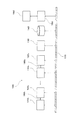
図1には、一実施形態のリソグラフィシステム100の構成が概略的に示されている。このリソグラフィシステム100は、N台の投影露光装置1101〜110N、各投影露光装置110i(i=1〜N)毎に併設されたマシンコントローラ(MC)1201〜120N、像歪み演算装置130、集中情報サーバ140、ターミナルサーバ150、及びプロセス管理装置としてのホスト計算機160を備えて構成される。ここで、投影露光装置110i、MC120i、像歪み演算装置130、集中情報サーバ140、及びターミナルサーバ150は、ローカルエリアネットワーク(LAN)170に接続されており、また、ホスト計算機160は、ターミナルサーバ150を介してLAN170に接続されている。すなわち、ハードウエア構成上では、投影露光装置110i、MC120i、像歪み演算装置130、集中情報サーバ140、ターミナルサーバ150、及びホスト計算機160の相互間の通信経路が確保されている。なお、本システムにおける実際の構成要素相互間の通信については後述する。
【0020】
前記投影露光装置1101〜110Nのそれぞれはステップ・アンド・リピート方式の投影露光装置(いわゆる「ステッパ」)であってもよいし、また、ステップ・アンド・スキャン方式の投影露光装置(以下、「走査型露光装置」という)であってもよい。但し、投影露光装置1101〜110Nの少なくとも1つは、投影像の歪みの調整能力を有していることが必要である。なお、以下の説明においては、投影露光装置1101〜110Nの全てが、投影像の歪み調整能力を有する走査型露光装置であるとする。
【0021】
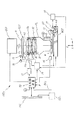
図2には、かかる投影露光装置1101〜110Nの中の1台の投影露光装置1101の概略的な構成が示されている。なお、他の投影露光装置1102〜110Nも投影露光装置と同様に構成される。図2に示されるように、投影露光値1101は、照明系IOP、マスクとしてのレチクルRを保持するレチクルステージRST、投影光学系PL、感応基板としてのウエハWが搭載されるウエハステージWST等を備えている。
【0022】
前記照明系IOPは、光源、フライアイレンズ等からなる照度均一化光学系、リレーレンズ、可変NDフィルタ、レチクルブラインド、及びダイクロイックミラー等(いずれも不図示)を含んで構成されている。こうした照明系の構成は、例えば、特開平10−112433号公報に開示されている。
【0023】
この照明系IOPでは、回路パターン等が描かれたレチクルR上のレチクルブラインドで規定されたスリット状の照明領域部分を照明光ILによりほぼ均一な照度で照明する。
【0024】
前記レチクルステージRST上にはレチクルRが、例えば真空吸着により固定されている。レチクルステージRSTは、ここでは、磁気浮上型の2次元リニアアクチュエータから成る不図示のレチクルステージ駆動部によって、レチクルRの位置決めのため、照明光学系の光軸(後述する投影光学系PLの光軸AXに一致)に垂直なXY平面内で微少駆動可能であるとともに、所定の走査方向(ここではY方向とする)に指定された走査速度で駆動可能となっている。さらに、本実施形態では上記磁気浮上型の2次元リニアアクチュエータはX駆動用コイル、Y駆動用コイルの他にZ駆動用コイルを含んでいるため、Z方向にも微小駆動可能となっている。
【0025】
レチクルステージRSTのステージ移動面内の位置はレチクルレーザ干渉計(以下、「レチクル干渉計」という)16によって、移動鏡15を介して、例えば0.5〜1nm程度の分解能で常時検出される。レチクル干渉計16からのレチクルステージRSTの位置情報はステージ制御系19に送られ、ステージ制御系19はレチクルステージRSTの位置情報に基づいてレチクルステージ駆動部(図示省略)を介してレチクルステージRSTを駆動する。
【0026】
前記投影光学系PLは、レチクルステージRSTの図2における下方に配置され、その光軸AXの方向がZ軸方向とされ、ここでは両側テレセントリックな光学配置となるように光軸AX方向に沿って所定間隔で配置された複数枚のレンズエレメント27、29、30、31、……及びこれらのレンズエレメント27、29、30、31、……を保持するレンズ鏡筒32を含んで構成されている。この投影光学系PLは所定の投影倍率、例えば1/5(あるいは1/4)を有する縮小光学系である。このため、照明系IOPからの照明光ILによってレチクルRの照明領域が照明されると、このレチクルRを通過した照明光ILにより、投影光学系PLを介して照明領域部分のレチクルRの回路パターンの縮小像(部分倒立像)が表面にレジスト(感光剤)が塗布されたウエハW上に形成される。この投影露光装置1101では、この投影光学系PLによる投影像の歪み(倍率を含む)を補正する結像特性補正装置が設けられている(これについては、後に詳述する)。
【0027】
前記ウエハステージWSTは、投影光学系PLの図2における下方に配置され、このウエハステージWST上には、ウエハホルダ9が保持されている。このウエハホルダ9上にはウエハWが真空吸着されている。ウエハホルダ9は不図示の駆動部により、投影光学系PLの最良結像面に対し、任意方向に傾斜可能で、かつ投影光学系PLの光軸AX方向(Z方向)に微動が可能に構成されている。また、このウエハホルダ9は光軸AX回りの回転動作も可能になっている。
【0028】
ウエハステージWSTは走査方向(Y方向)の移動のみならず、ウエハW上の複数のショット領域を前記照明領域IARと共役な露光領域IAに位置させることができるように、走査方向に垂直な方向(X方向)にも移動可能に構成されており、ウエハW上の各ショット領域を走査(スキャン)露光する動作と、次のショットの露光開始位置まで移動する動作とを繰り返すステップ・アンド・スキャン動作を行う。このウエハステージWSTはモータ等のウエハステージ駆動部(不図示)によりXY2次元方向に駆動される。
【0029】
ウエハステージWSTのXY平面内での位置はウエハレーザ干渉計18によって、移動鏡17を介して、例えば0.5〜1nm程度の分解能で常時検出されている。ウエハステージWSTの位置情報(又は速度情報)はステージ制御系19に送られ、ステージ制御系19はこの位置情報(又は速度情報)に基づいてウエハステージWSTを制御する。
【0030】
上記のように構成された投影露光装置1101においては、前記スリット状の照明領域(中心は光軸AXとほぼ一致)を照明光ILにより照明した状態で、ウエハWとレチクルRとを走査方向(Y方向)に沿って互いに逆向きに、投影倍率に応じた速度比で同期移動する。かかる走査露光により、レチクルRのパターン領域のパターンがウエハW上のショット領域上に縮小転写される。
【0031】
投影光学系PLの側面には、ウエハW上の各ショット領域に付設されたアライメントマーク(ウエハマーク)の位置を検出するためのオフ・アクシス方式のアライメント顕微鏡、例えば画像処理方式の結像式アライメントセンサ8が設けられている。主制御装置50では、上記の走査露光に先立って、ウエハマークの計測された位置に基づいて例えば特開昭61−44429号公報に開示される統計演算によりウエハW上のショット領域の配列座標を算出する。
【0032】
また、投影露光装置1101には、投影光学系PLの最良結像面に向けて複数のスリット像を形成するための結像光束を光軸AX方向に対して斜め方向より供給する照射光学系13と、その結像光束のウエハWの表面での各反射光束をそれぞれスリットを介して受光する受光光学系14とから成る斜入射方式の多点焦点位置検出系が、投影光学系PLを支える支持部(図示省略)に固定されている。この多点焦点位置検出系(13、14)としては、例えば特開平5−190423号公報に開示されるものと同様の構成のものが用いられ、ステージ制御系19はこのウエハ位置情報に基づいてウエハホルダ9をZ方向及び傾斜方向に駆動する。
【0033】
次に、投影学系PLの結像特性を補正するための結像特性補正装置について説明する。この結像特性補正装置は、大気圧変化、照明光吸収等による投影光学系PL1自体の結像特性の変化を補正すると共に、ウエハW上の前層の露光ショット(ショット領域)の歪みに合わせてレチクルRのパターンの投影像を歪ませる働きをもつ。投影光学系PLの結像特性としては焦点位置、像面湾曲、ディストーション、非点収差等があり、それらを補正する機構はそれぞれ考えられるが、以下の説明においては結像特性補正装置は、主として投影像の歪み(倍率を含む)に関する補正のみを行なうものとする。
【0034】
図2において、投影光学系PLを構成する、レチクルRに最も近いレンズエレメント27は支持部材28に固定され、レンズエレメント27に続くレンズエレメント29,30,31,…は投影光学系PLのレンズ鏡筒32に固定されている。支持部材28は、伸縮自在の複数(ここでは3つ)の駆動素子、例えばピエゾ素子11a、11b、11c(但し、図2では紙面奥側の駆動素子11cは図示せず)を介して投影光学系PLのレンズ鏡筒32と連結されている。駆動素子11a、11b、11cに印加される駆動電圧が結像特性制御部12によって独立して制御され、これによって、レンズエレメント27が光軸AXに直交する面に対して任意に傾斜及び光軸方向に移動可能な構成となっている。各駆動素子によるレンズエレメント27の駆動量は不図示の位置センサにより厳密に測定され、その位置はサーボ制御により目標値に保たれるようになっている。
【0035】
この投影露光装置1101ではレンズエレメント27の支持部材28、駆動素子11a、11b、11c及びこれに対する駆動電圧を制御する結像特性制御部12によって結像特性補正装置(倍率調整手段を兼ねる)が構成されている。なお、投影光学系PLの光軸AXとはレンズエレメント29以下のレンズエレメントの共通の光軸を指すものとする。
【0036】
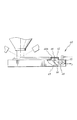
次に、投影像の歪みを測定を計測するため、レチクルRに形成された計測マーク(マークパターン)の投影光学系PLを介しての投影像を光電検出する空間像計測器60について、図3に基づいて説明する。
【0037】
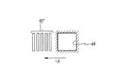
図3には、この空間像計測器60を含む図2のウエハステージWST近傍部分が拡大して示されている。図3において、ウエハステージWSTの一端部上面には、上部が開口した突設部が設けられており、この突設部の開口を塞ぐ状態で受光ガラス62が嵌め込まれている。この受光ガラス62の上面は、その周辺部にクロム層により形成された遮光帯64aが形成され、中央部にほぼ正方形の開口パターン64が形成されている。
【0038】
開口パターン64の下方のウエハステージ50内部には、レンズ66、68から成るリレー光学系と、このリレー光学系(66、68)によって所定光路長分だけリレーされる照明光束(像光束)の光路を折り曲げる折り曲げミラー69とから成る受光光学系と、シリコンフォトダイオード又はフォトマルチプライヤ等の光電変換素子から成る光電センサ70が配置されている。
【0039】
本実施形態では、上記ウエハステージWSTの一端部上面の突設部、受光ガラス62、受光ガラス62上の遮光帯64aによって形成された開口パターン64、リレー光学系(66、68)、折り曲げミラー69及び光電センサ70によって空間像計測器60が構成されている。
【0040】
この空間像計測器60によれば、レチクルRに形成された計測パターンの投影光学系PLを介しての投影像の検出の際には、投影光学系PLを透過してきた照明光ILが受光ガラス62を照明し、受光ガラス62上の開口パターン64を透過した照明光ILが上記受光光学系を通って光電センサ70に到達し、光電センサ70では光電変換を行い受光量に応じた光量信号Pを主制御装置50に出力する。
【0041】
次に、上記の空間像計測器60を用いた投影像の歪みの検出方法の一例について説明する。
【0042】
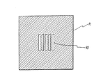
前提として、ここではレチクルR上に図4に示されるような5本のバーマークから成るラインアンドスペース(L/S)のマークパターンとしての計測マーク90が形成されているものとする。図4において斜線部(影線部)は遮光帯を表している。
【0043】
この投影像の検出は、投影光学系PLの光軸AXの直下に受光ガラス62上の開口パターン64のウエハホルダ9側の遮光部64aが位置するように、ウエハステージWSTを移動した状態で開始される。
【0044】
この開始位置では、照明系IOPからの照明光ILにより計測マーク90が照明されると、この計測マーク90部分(5本のバーマーク)を透過した照明光ILによってウエハステージWST上の受光ガラス62上の開口パターン64のウエハホルダ52側の遮光部64aに計測マーク90の投影像90’が結像される。このときの状態が、図5に示されている。
【0045】
そして、主制御装置50からの指示に応じて、ステージ制御系19ではステージ駆動系を介してウエハステージWSTを−X方向に所定速度で移動させる。これにより計測マーク90の投影像90’の右側から徐々に開口パターン64に重なるようになる。計測マーク90の投影像90’と開口パターン64の重なりが増すにつれて、光電センサ70に入射する光量が増加していき、計測マーク90の投影像90’と開口パターン64とがちょうど重なった時が最大光量となる。その後、更にウエハステージWSTが−X方向に移動すると、今度は光電センサ70に入射する光量が徐々に減っていき、計測マーク90の投影像90’と開口パターン64の重なりがなくなった時に光電センサ70に入射する光量は0となる。
【0046】
この時の光量の変化が図6(A)に示されている。主制御装置50では、この図6(A)に示されるような光量信号Pの波形(実際には、所定のサンプリング間隔で取り込まれたディジタルデータである)を走査方向に対して微分することで図6(B)に示されるような微分波形を計算する。この図6(B)から明らかなように、開口パターン64の走査方向前側のエッジが計測マークの投影像90’を横切っている状態では徐々に光量が増加する、即ち微分波形がプラス側となる。この反対に、開口パターン64の走査方向後側のエッジが計測マーク90の投影像90’を横切っている状態では徐々に光量が減少する、即ち微分波形がマイナス側となる。
【0047】
そして、主制御装置50では図6(B)に示されるような微分波形に基づいてフーリエ変換法などの公知の信号処理を施し、計測マーク90が投影された光学像(空間像)を検出する。
【0048】
以上説明したような検出方法を用いて、レチクルR上に配置された複数の計測マークの投影像(空間像)を検出することにより、投影光学系PLの倍率やディストーション等の結像特性を含めた投影像の歪みを測定する。
【0049】
図2に戻り、主制御装置50はLAN170に接続されており、また、LAN170とは別経路で設けられた通信路180を介してMC1201に接続されている。そして、主制御装置50は、通信路180を介して、MC1201からの動作パラメータを受信したり、露光動作の経過や結果をMC1201に送信したりする。また、主制御装置50は、LAN170を介して、集中情報サーバ140へ投影像の歪みの測定結果を送信する。
【0050】
図1に戻り、前記MC1201〜120Nのそれぞれは、通常のパーソナルコンピュータと同様に構成される。各MC120iは、通信路180を介した対応する投影露光装置110iとの間の通信の他に、LAN170を介して、像歪み演算装置130との間で通信を行い、対応する投影露光装置110iの動作パラメータの問い合わせを行い、また、像歪み演算装置130から対応する投影露光装置110iの動作パラメータを受信する。なお、各MC120iは、各投影露光装置110iと対で設置される不図示のコータ/デベロッパをも管理している。
【0051】
前記像歪み演算装置130は、演算能力に優れた中規模の計算機システム(例えば、ミニコン・システムやエンジニアリング・ワークステーション・システム)によって構成されている。この像歪み演算装置130は、LAN170を介した上記のMC1201〜120Nとの通信の他に、LAN170及びターミナルサーバ150を介して、ホスト計算機160との間で通信を行い、ホスト計算機160からの露光ロットの指定情報を受信し、また、指定された露光ロットの露光に適切な投影露光装置の候補を決定し、この決定結果をホスト計算機160へ送信する。また、像歪み演算装置130は、LAN170を介して、集中情報サーバ140との間で通信を行い、後述するデータの授受を行う。
【0052】
前記集中情報サーバ140は、大容量記憶装置とLANインターフェースとから構成される。大容量記憶装置には、像歪み演算装置130によって管理されるウエハWのロットに関する露光履歴データを記憶している。露光履歴データには、各ウエハロットに関する各層の露光時における投影像の歪みデータが含まれている。さらに、大容量記憶装置には、使用するレチクルの描画誤差等を記憶している。
【0053】
本実施形態では、この各層の露光時における投影像の歪みデータは、各層の露光で使用された投影露光装置の投影光学系PLに関する投影像の歪み調整パラメータと、使用されたレチクルの描画誤差と、その投影露光装置において、前述の空間像計測器60を使用して定期的(例えば、1回/日、1回/週、1回/月等)に所定値の露光条件で測定された投影像歪みデータとに基づいて、像歪み演算装置130によって算出され、集中情報サーバ140の大容量記憶装置に格納される。なお、像歪み演算装置130及び集中情報サーバ140を含んで歪み管理装置が構成されている。
【0054】
前記ターミナルサーバ150は、LAN170における通信プロトコルとホスト計算機160の通信プロトコルとの相違を吸収するためのゲートウエイプロッセサとして構成される。このターミナルサーバ150の機能によって、ホスト計算機160と、LAN170に接続されたMC1201〜120N及び像歪み演算装置130との間の通信が可能となる。
【0055】
前記ホスト計算機160は大型の計算機で構成され、例えば、リソグラフィ工程を含め、工場内における半導体素子等の製造にあたっての統括制御を行っている。なお、像歪み演算装置130、集中情報サーバ140、及び前記ホスト計算機160を含んで判定装置が構成されている。
【0056】
前記LAN170には、バス型LAN及びリング型LANのいずれも採用可能であるが、本実施形態では、IEEE802規格のキャリア敏感型媒体アクセス/競合検出(CSMA/CD)方式のバス型LANを使用している。また、通信経路180には、シリアル型及びパラレル型のいずれの方式の通信経路も採用可能であるが、本実施形態では、RS232C規格のシリアル型通信路を使用している。
【0057】
次に、以上のように構成された本実施形態のリソグラフィシステム100によるウエハWの露光処理のアルゴリズムを、図7に基づいて説明する。
【0058】
なお、図7に示された露光処理のアルゴリズムの実行の前提として、露光対象となるウエハWは、既に1層以上の露光が行われたものであり、また、ウエハWの露光履歴データ、各投影露光装置1101〜110Nに関する投影像の歪みデータ、及び転写対象となるレチクルRに形成されたパターンの描画誤差は集中情報サーバ140に記憶されているものとする。
【0059】
まず、図7のステップ201において、ホスト計算機160が、重ね合わせ露光の対象となるウエハWのロットの識別子(例えば、ロット番号)と、重ね合わせ露光にあたって重ね合わせ精度を確保すべき1層以上の露光済み層(以後、「基準層」という)と、使用するレチクルの識別子(例えば、レチクル番号)とを指定して、該ロット番号のウエハWの露光を行うのに適切な投影露光装置を、ターミナルサーバ150及びLAN170を介して像歪み演算装置130に問い合わせる。
【0060】
次に、ステップ203において、像歪み演算装置130は、受信したロット識別子及び基準層に応じて、集中情報サーバ140からウエハWのロットの露光履歴情報の中から、各基準層の露光に関する投影像の歪みデータをLAN170を介して読み出す。また、像歪み演算装置130は、受信したレチクル識別子に応じて、集中情報サーバ140から使用するレチクルRの描画誤差をLAN170を介して読み出す。
【0061】
引き続き、像歪み演算装置130は、読み出されたレチクルRの描画誤差を加味しつつ、各投影露光装置110iにおける投影像の歪みが、基準層の露光時において発生していた投影像の歪みとの差が最小となる歪み調整パラメータ値を各投影露光装置110i毎に算出する。ここで、基準層が複数あるときは、各基準層の露光時において発生していた投影像の歪みを統計処理(例えば、平均演算)して、重ね合わせの基準とする投影像の歪みを求める。
【0062】
そして、算出された各投影露光装置110iに関する歪み調整パラメータ値が、各投影露光装置110iの調整能力範囲であるか否かを判定し、肯定的に判定された場合には、算出された歪み調整パラメータ値を適用したときの投影像の歪みと基準層の露光時において発生していた投影像の歪みとの差をそれらの投影露光装置110iの残留誤差として求める。一方、否定的に判定された場合には、それらの投影露光装置の調整能力の範囲内で、基準層の露光時において発生していた投影像の歪みとの差が最小となる投影像の歪みとなる歪み調整パラメータ値を算出し、これらの歪み調整パラメータ値を適用したときの投影像の歪みと基準層の露光時において発生していた投影像の歪みとの差をそれらの投影露光装置110iの残留誤差として求める。すなわち、全ての投影露光装置110iのそれぞれについて、投影像の歪み調整能力の範囲内における最良の歪み調整パラメータ値と残留誤差とを求める。
【0063】
次いで、像歪み演算装置130は、各残留誤差と所定の許容誤差とを比較し、残留誤差が許容誤差以下である投影露光装置を、重ね合わせ露光を行う投影露光装置の候補として決定する。
【0064】
そして、ステップ205において、決定された投影露光装置のリストを候補リストとしてホスト計算機160へLAN170及びターミナルサーバ150を介して送信する。
【0065】
次に、ステップ207において、ホスト計算機160が、受信した候補リストに挙げられた投影露光装置について現在の稼動状況及び将来の稼動予定を参照し、リソグラフィシステムとして最も効率良くリソグラフィ工程を進行させる観点から、重ね合わせ露光を行う投影露光装置を選択する。例えば、ホスト計算機160は、候補リストに挙げられた投影露光装置の内で、現在稼動していない投影露光装置があれば、その投影露光装置を選択する。また、候補リストに挙げられた投影露光装置が全て稼動中の場合には、ホスト計算機160は、例えば、最も早く現在の露光動作が完了する予定の投影露光装置を選択する。
【0066】
上記のステップ205において、像歪み演算装置130は、候補リストに加えて、候補リストに挙げられた各投影露光装置の残留誤差もホスト計算機160に送信するようにすることもできる。この場合には、ステップ207において、ホスト計算機は、リソグラフィシステムにおける処理効率と露光精度とを総合的に勘案して、重ね合わせ露光を行う投影露光装置を選択することができる。例えば、候補リストに挙げられた投影露光装置の複数が現在稼動していないときには、その中で残留誤差が最小のものを選択することにより、処理効率を確保しつつ露光精度を高めることができる。
【0067】
なお、以下では、投影露光装置1101が選択された場合を例にして説明を行う。
【0068】
そして、ステップ209において、ホスト計算機160は、選択した投影露光装置1101が稼動中でなければ直ちに、また、選択した投影露光装置1101が稼動中の場合には露光動作の終了を待って、重ね合わせ露光の対象となるウエハWのロットの識別子を指定して選択した投影露光装置1101と接続されたMC1201にLAN170を介して露光実行の指示を行う。
【0069】
次に、ステップ211において、露光実行の指示を受信したMC1201は、重ね合わせ露光の対象となるウエハWのロットの識別子及び投影露光装置1101の識別子を指定して、当該ロットのウエハWを露光するにあたっての投影像の歪みの調整パラメータ値を像歪み演算装置130に問い合わせる。なお、投影露光装置110iとMC120iとは1対1に対応するので、MC1201は、投影露光装置1101の識別子に代えて、MC1201の識別子を指定することも可能である。
【0070】
次いで、ステップ213において、像歪み演算装置130は、受信したウエハWのロットの識別子に応じて、そのウエハWのロットについてステップ203で算出された、選択された投影露光装置1101に関する歪み調整パラメータをMC1201へLAN170を介して送信する。この送信と相前後して、重ね合わせ露光前に、像歪み演算装置130は、当該ロットの当該重ね合わせ露光における投影像の歪みを特定し、この投影像の歪みデータをLAN170を介して集中情報サーバ140に格納し、当該ロットの露光履歴情報を仮に更新する。そして、後にMC1201から露光の正常終了が通知されると、当該ロットの露光履歴情報の仮更新を本更新に変更する。
【0071】
次に、ステップ215において、MC1201は、受信した歪み調整パラメータを通信路1801を介して投影露光装置1101へ送信する。そして、投影露光装置1101は、受信した歪み調整パラメータに基づいて、自身の結像特性補正装置を制御して、投影像の歪みを調整する。この後、ステップ217において、投影像の歪みが調整された投影露光装置1101によって、レチクルRに形成されたパターンが、重ね合わせ露光により、ウエハWに転写される。
【0072】
以上説明したように、本実施形態のリソグラフィシステム100では、各ウエハWのロットに関する重ね合わせ露光の都度、露光済みの基準層の露光において発生した投影像の歪みに対して、残留誤差を許容範囲におさめることができ、かつ、リソグラフィシステムの処理効率向上の観点からも適切な投影露光装置を選択することができる。したがって、高い重ね合わせ精度を確保しつつ、量産性を向上することができる。
【0073】
なお、上記の実施形態では、複数の投影露光装置の全てを走査型露光装置としたが、全ての投影露光装置がステップ・アンド・リピート方式のステッパであってもよいし、また、走査型露光装置とステッパとが混在してもよい。但し、走査型露光装置とステッパとが混在したり、全ての露光装置がステッパであってもフィールドサイズが異なる場合には、投影像の歪みの測定にあたっての測定位置が異なるので、投影像の歪みの直接的な比較ができないことがある。その場合は、こで、投影像の歪みの適切なモデル(例えば、3次モデル)から、必要な位置における投影像の歪みを求めて、比較すれば良い。
【0074】
また、上記の実施形態では、複数の投影露光装置の全てが投影像の歪みの調整能力を有するものととしたが、少なくとも1つの投影露光装置が投影像の歪みの調整能力を有すればよい。投影像の歪みの調整能力が無い投影露光装置が混在する場合には、それらについては、候補リストの作成にあたって、歪み調整パラメータの最良値の算出を行わず、投影像の歪みの測定値を使用して残留誤差を求めることにすればよい。
【0075】
また、上記の実施形態では、投影像の歪み調整にあたっては、投影光学系の結像特性を調整することにしたが、レチクルとウエハとの同期移動状態を調整することにより、投影像の歪みを調整してもよい。さらに、投影光学系の結像特性及びレチクルとウエハとの同期移動状態の双方を調整することにより、投影像の歪みを調整してもよい。
【0076】
また、上記の実施形態では、投影光学系の結像特性の調整で、投影光学系のレンズ要素を駆動したが、投影光学系内の露光光の光路上の一部の密閉室内のガス圧を制御してその部分の屈折を調整することにより、投影光学系の結像特性を調整してもよい。
【0077】
また、上記の実施形態では、各投影露光装置の投影像の歪みの測定を、定期的に行うことにしたが、各ウエハのロットの各層の露光ごとに、歪み調整パラメータの算出の直前に行ってもよい。
【0078】
また、上記の実施形態では、各投影露光装置の投影像の歪みの測定を、空間像計測器を使用した空間像検出によって行ったが、測定用レチクルに形成された測定用パターンを測定用のウエハに実際に転写し、ウエハ上に転写されたパターンを計測することにより、投影像の歪みを測定することも可能である。
【0079】
さらに、投影露光装置が、空間像計測器による空間像検出の機能を有する場合には、デバイス製造用のレチクルにも位置検出マークを形成し、この位置検出マークの空間像を検出することにより、投影露光装置で各レチクルの使用の度に、投影像の歪み計測とレチクルの位置合わせとを精度良く行うこともできる。
【0080】
また、投影露光装置の露光対象は上記の実施形態のように半導体製造用のウエハに限定されることなく、例えば、液晶表示素子パターンの露光用の角型のガラスプレートや、薄膜磁気へッドを製造するための基板にも広く適用できる。
【0081】
また、上記の実施形態の投影露光装置における照明光ILとしては、g線(436nm)、i線(365nm)、KrFエキシマレーザ光(248nm)、ArFエキシマレーザ光(193nm)、F2レーザ光(157nm)、X線や電子線等の荷電粒子線を用いることができる。例えば、電子線を用いる場合には電子銃として、熱電子放射型のランタンへキサボライト(LaB6)、夕ンタル(Ta)を用いることができる。
【0082】
また、投影光学系の倍率は縮小系のみならず等倍および拡大系のいずれでもいい。
【0083】
また、投影光学系としては、KrF、ArFエキシマレーザ光などの遠紫外線を用いる場合は硝材として石英や蛍石などの遠紫外線を透過する材料を用い、F2レーザ光やX線を用いる場合は反射屈折系または反射系の光学系にし(レチクルも反射型タイプのものを用いる)、また、電子線を用いる場合には光学系として電子レンズ及び偏向器からなる電子光学系を用いればよい。なお、電子線が通過する光路は真空状態にすることはいうまでもない。
【0084】
また、ウエハステージやレチクルステージにリニアモータ(米国特許番号第5,623,853号公報または米国特許番号第5,528,118号公報参照)を用いる場合は、エアべアリングを用いたエア浮上型およびローレンツ力又はリアクタンス力を用いた磁気浮上型のどちらを用いてもよい。また、ウエハステージやレチクルステージは、ガイドに沿って移動するタイブでもいいし、ガイドを設けないガイドレスタイプでもいい。
【0085】
また、ウエハステージの移動により発生する反力は、(米国特許番号第5,528,118号公報に記載されているように、)フレーム部材を用いて機械的に床(大地)に逃がしてもいい。また、レチクルステージの移動により発生する反力は、特開平8−166475号公報(米国特許出願シリアル番号第08/416,558号)に記載されているように、フレーム部材を用いて機械的に床(大地)に逃がしてもいい。
【0086】
なお、複数のレンズから構成される照明光学系、投影光学系を投影露光装置本体に組み込み光学調整をするとともに、多数の機械部品からなるレチクルステージやウエハステージを投影露光装置本体に取り付けて配線や配管を接続し、更に総合調整(電気調整、動作確認等)をすることにより、本実施形態の投影露光装置、ひいては本実施形態のリソグラフィシステムを製造することができる。なお、投影露光装置の製造は温度およびクリーン度等が管理されたクリーンルームで行うことが望ましい。
【0087】
また、半導体デバイスは、デバイスの機能・性能設計を行うステップ、この設計ステップに基づいたレチクルを制作するステッブ、シリコン材料からウエハを製作するステップ、前述した実施形態のリソグラフィシステムによりレチクルのパターンをウエハに露光するステッブ、デバイス組み立てステップ(ダイシング工程、ボンディング工程、パッケージ工程を含む)、検査ステッブ等を経て製造される。
【0088】
【発明の効果】
以上、詳細に説明したように、本発明の露光方法によれば、少なくとも1層以上の露光がなされた感応基板に関する重ね合わせ露光に際し、重ね合わせ露光の対象となる感応基板が、それまでどのような投影露光装置で露光されてきたかを示す露光履歴と、各投影露光装置のそれぞれの歪み調整能力とに基づいて、重ね合わせ精度を高精度に確保できる投影露光装置を選択する。したがって、複数の投影露光装置を使用しつつ、高い重ね合せ精度で重ね合わせ露光を行うことができる。
【0089】
さらに、重ね合わせ露光を行う投影露光装置の選択にあたって、各投影露光装置の稼動状況を考慮することにより、高い重ね合わせ精度を確保しつつ、露光処理のスループットを向上することができる。
【0090】
また、本発明のリソグラフィシステムによれば、重ね合わせ露光に際して、判定装置が、重ね合わせ露光の対象となる感応基板の露光履歴と、各投影露光装置のそれぞれの歪み調整能力とに基づいて、重ね合わせ精度を高精度に確保できる投影露光装置を選択する。すなわち、本発明の露光方法を使用して、感応基板の重ね合わせ露光を行うので、複数の投影露光装置を使用しつつ、高い重ね合せ精度で重ね合わせ露光を行うことができる。
【図面の簡単な説明】
【図1】一実施形態のリソグラフィシステムの概略的な構成を示す図である。
【図2】図1の投影露光装置の概略的な構成を示す図である。
【図3】図2のウエハステージ近傍部分を拡大して示す図である。
【図4】レチクル上に形成された計測マークの一例を示す図である。
【図5】図4の計測マークの投影像の光電検出方法を説明するための図である。
【図6】(A)は図4の計測マークの投影像の光電検出した結果得られた光量信号の波形を示す線図、(B)は(A)の微分波形を示す線図である。
【図7】一実施形態のリソグラフィシステムで行われる露光処理のアルゴリズムのフローチャートである。
【符号の説明】
110…投影露光装置、130…像歪み演算装置(歪み管理装置の一部、判定装置の一部)、140…集中情報サーバ(歪み管理装置の一部、判定装置の一部)、160…ホスト計算機(プロセス管理装置、判定装置の一部)[0001]
BACKGROUND OF THE INVENTION
The present invention relates to an exposure method and a lithography system, and more particularly to a lithography system and an exposure method used in a lithography process when manufacturing a microdevice such as a semiconductor element or a liquid crystal display element.
[0002]
[Prior art]
Conventionally, in a lithography process for manufacturing a semiconductor element, a liquid crystal display element or the like, a resist or the like is applied to a pattern formed on a mask or a reticle (hereinafter, collectively referred to as “reticle”) via a projection optical system. A projection exposure apparatus that transfers onto a substrate such as a wafer or a glass plate (hereinafter referred to as “sensitive substrate or wafer” as appropriate) is used. In order to increase mass productivity, it is generally performed to prepare a plurality of projection exposure apparatuses and construct a lithography system in which these projection exposure apparatuses are managed by a host computer.
[0003]
Here, in the manufacture of semiconductor elements, etc., different circuit patterns are formed by stacking several layers on a sensitive substrate, but in order to increase mass productivity, the circuit pattern of each layer (layer) on one substrate is changed. It is necessary to transfer using a different projection exposure apparatus. Therefore, it is necessary to match the distortion of the transferred image between the projection exposure apparatuses in order to ensure the overlay accuracy.
[0004]
In a conventional lithography system, in order to ensure overlay accuracy by reducing machine differences in transferred images, when carrying in each projection exposure apparatus, the distortion of the transfer image by each projection exposure apparatus is brought close to the ideal value as much as possible. The projection optical system of the other projection exposure apparatus is adjusted so that distortion similar to the distortion of the transfer image in this reference machine is generated by adjusting one of the projection optical systems or the like. Etc. were adjusted.
[0005]
As a method for adjusting the distortion of the transfer image of such a projection exposure apparatus, for example, as an example of a collective exposure apparatus, a part of the lens elements of the projection optical system is driven in the optical axis direction or with respect to a plane orthogonal to the optical axis. A method and apparatus for generating image distortion by tilting is described in JP-A-4-127514. As an example in a scanning exposure apparatus, the magnification of the projection optical system is continuously changed during scanning exposure, the relative angle in the scanning direction of the reticle and the substrate is offset, or the relative angle is continuously set. Japanese Patent Laid-Open No. 7-57991 discloses a method and an apparatus for applying distortion to an image formed after scanning.
[0006]
[Problems to be solved by the invention]
In the above-described conventional lithography system, the distortion of the transferred image by each projection exposure apparatus is small compared to the distortion of the reference transfer image, that is, the ideal value distortion or the distortion of the reference machine. A difference of about the sum may exist between the projection exposure apparatuses. Furthermore, the transfer characteristics of the projection exposure apparatus change with time, and the mechanical difference in distortion of the transferred image between the projection exposure apparatuses may increase with time.
[0007]
For this reason, in the matching of the transfer image using the adjustment value of the distortion of the transfer image at the time of introduction of each projection exposure apparatus, which has been performed in the conventional lithography system, the overlay accompanying the miniaturization of the circuit pattern which has been increasing in recent years. It is becoming difficult to meet the demand for improved alignment accuracy.
[0008]
The present invention has been made under such circumstances, and an object thereof is to provide an exposure method and a lithography system capable of performing overlay exposure with high overlay accuracy while using a plurality of projection exposure apparatuses. It is in.
[0009]
[Means for Solving the Problems]
The exposure method of the present invention includes a plurality of projection exposure apparatuses (110) including at least one projection exposure apparatus capable of adjusting distortion of a projected image. 1 ~ 110 N In the exposure method in which the sensitive substrate (W) is exposed in a multi-layered manner in the above-described manner, the overlay exposure of the sensitive substrate (W) on which at least one layer of exposure has been performed, The projection image distortion adjustment parameter for the projection optical system of the projection exposure apparatus that has exposed the sensitive substrate, the drawing error of the pattern formed on the used mask, and the exposure condition of the predetermined value regularly in the projection exposure apparatus. Calculated based on the measured projection image distortion data, An exposure history of the sensitive substrate (W) including distortion information of a projected image at the time of exposure of the projection exposure apparatus that has exposed the sensitive substrate, and the plurality of projection exposure apparatuses (110 1 ~ 110 N ) Selecting from among the plurality of projection exposure apparatuses a projection exposure apparatus for superposing and exposing the sensitive substrate on the basis of the respective distortion adjustment capabilities and the drawing error of the pattern formed on the mask; To do.
[0010]
According to this, at the time of overlay exposure on a sensitive substrate having at least one layer of exposure, for example, one lot of sensitive substrates, the sensitive substrate to be subjected to the overlay exposure is determined by what projection exposure apparatus. Exposure history showing how the exposure has been Including distortion information of a projected image at the time of exposure of the projection exposure apparatus that has exposed the sensitive substrate of the plurality of projection exposure apparatuses) From this, know the distortion of the transferred image in each layer, and then in view of the respective distortion adjustment capabilities of each projection exposure apparatus, And considering the drawing error of the pattern formed on the mask, A projection exposure apparatus capable of ensuring high overlay accuracy is selected. Then, using the selected projection exposure apparatus, overlay exposure of the sensitive substrate is performed. Therefore, overlay exposure can be performed with high overlay accuracy while using a plurality of projection exposure apparatuses.
[0012]
Further, when selecting a projection exposure apparatus that performs overlay exposure, for each projection exposure apparatus, the overlay error with the projection image of the projection exposure apparatus that has exposed the sensitive substrate to be subjected to overlay exposure is minimized. Thus, by obtaining the residual error when the distortion is adjusted and selecting a projection exposure apparatus that performs overlay exposure based on the value of each residual error, an appropriate projection exposure apparatus can be selected. In such a case, the exposure that is the residual error of the selected projection exposure apparatus is adjusted to perform overlay exposure.
[0013]
Also , Throw A projection exposure apparatus that performs the overlay exposure is selected by comprehensively determining the operation accuracy of each projection exposure apparatus at the time of selection of the shadow exposure apparatus and the matching accuracy of the transfer image error in the exposure that has already been performed. Thus, mass productivity can be improved while ensuring high overlay accuracy.
[0014]
The lithography system of the present invention includes a plurality of projection exposure apparatuses (110) including at least one projection exposure apparatus capable of adjusting distortion of a projection image. 1 ~ 110 N And at the time of overlay exposure of the sensitive substrate (W) on which at least one layer of exposure has been performed, of the plurality of projection exposure apparatuses. The projection image distortion adjustment parameter for the projection optical system of the projection exposure apparatus that has exposed the sensitive substrate, the drawing error of the pattern formed on the used mask, and the exposure condition of the predetermined value regularly in the projection exposure apparatus. Calculated based on the measured projection image distortion data, An exposure history of the sensitive substrate (W) including distortion information of a projected image at the time of exposure of the projection exposure apparatus that has exposed the sensitive substrate, and the plurality of projection exposure apparatuses (110 1 ~ 110 N ) A determination device (130) that selects, from the plurality of projection exposure devices, a projection exposure device that superimposes and exposes the sensitive substrate based on each distortion adjustment capability and a drawing error of a pattern formed on the mask. , 140, 160) and;
[0015]
According to this, at the time of overlay exposure, the determination apparatus uses an exposure history (in what state the sensitive substrate to be subjected to overlay exposure has been exposed by what projection exposure apparatus) Including distortion information of a projected image at the time of exposure of the projection exposure apparatus that has exposed the sensitive substrate of the plurality of projection exposure apparatuses) When , Each distortion adjustment capability of each projection exposure apparatus Considering the drawing error of the pattern formed on the mask, On the basis of the above, a projection exposure apparatus capable of ensuring a high overlay accuracy is selected. That is, since the overlay exposure is performed on the sensitive substrate using the exposure method of the present invention, the overlay exposure can be performed with high overlay accuracy while using a plurality of projection exposure apparatuses.
[0016]
Here, the determination apparatus is configured to include a process management apparatus that manages operation states of the plurality of projection exposure apparatuses; and a distortion management apparatus that manages operation history of the plurality of projection exposure apparatuses and distortion setting of the projection image. Is possible.
[0017]
In such a case, the distortion management device shares the process of calculating the optimum distortion setting value at the time of exposure of the sensitive substrate for the projection exposure device that can adjust the distortion of the projected image based on the exposure history of the sensitive substrate. A configuration that contributes to selection of a projection exposure apparatus that performs overlay exposure is appropriate as a system load sharing. In this system configuration, for example, when the sensitive substrate is exposed, distortion management is performed on the sensitive substrate specified by the process management apparatus based on the exposure history and the distortion adjustment capability of each projection exposure apparatus. The apparatus determines one or more projection exposure apparatus candidates for performing overlay exposure from the viewpoint of overlay accuracy. Then, the process management apparatus can execute an exposure method for selecting one projection exposure apparatus from the determined projection exposure apparatuses based on the determined operating status of the projection exposure apparatus. According to this exposure method, mass productivity can be improved while ensuring high overlay accuracy.
[0018]
DETAILED DESCRIPTION OF THE INVENTION
Hereinafter, an embodiment of the present invention will be described with reference to FIGS.
[0019]
FIG. 1 schematically illustrates the configuration of a
[0020]
[0021]
FIG. 2 shows such a
[0022]
The illumination system IOP includes an illuminance uniforming optical system including a light source, a fly-eye lens, etc., a relay lens, a variable ND filter, a reticle blind, a dichroic mirror, and the like (all not shown). The configuration of such an illumination system is disclosed in, for example, Japanese Patent Laid-Open No. 10-112433.
[0023]
In this illumination system IOP, a slit-shaped illumination area defined by a reticle blind on a reticle R on which a circuit pattern or the like is drawn is illuminated with illumination light IL with a substantially uniform illuminance.
[0024]
On reticle stage RST, reticle R is fixed, for example, by vacuum suction. In this case, the reticle stage RST is configured such that an optical axis of an illumination optical system (an optical axis of a projection optical system PL described later) is used for positioning the reticle R by a reticle stage driving unit (not shown) composed of a magnetically levitated two-dimensional linear actuator. It can be driven minutely in the XY plane perpendicular to AX) and can be driven at a scanning speed designated in a predetermined scanning direction (here, Y direction). Further, in the present embodiment, the magnetically levitated two-dimensional linear actuator includes a Z driving coil in addition to the X driving coil and the Y driving coil, and therefore can be finely driven in the Z direction.
[0025]
The position of the reticle stage RST in the stage moving surface is always detected by a reticle laser interferometer (hereinafter referred to as “reticle interferometer”) 16 through the moving
[0026]
The projection optical system PL is disposed below the reticle stage RST in FIG. 2, and the direction of the optical axis AX is the Z-axis direction. Here, the projection optical system PL is along the optical axis AX direction so as to be a bilateral telecentric optical arrangement. A plurality of
[0027]
Wafer stage WST is arranged below projection optical system PL in FIG. 2, and wafer holder 9 is held on wafer stage WST. A wafer W is vacuum-sucked on the wafer holder 9. The wafer holder 9 can be tilted in an arbitrary direction with respect to the best imaging plane of the projection optical system PL by a drive unit (not shown) and can be finely moved in the optical axis AX direction (Z direction) of the projection optical system PL. ing. The wafer holder 9 can also be rotated around the optical axis AX.
[0028]
Wafer stage WST is not only moved in the scanning direction (Y direction), but also in a direction perpendicular to the scanning direction so that a plurality of shot areas on wafer W can be positioned in exposure area IA conjugate with illumination area IAR. It is configured to be movable also in the (X direction), and repeats the operation of scanning (scanning) exposing each shot area on the wafer W and the operation of moving to the exposure start position of the next shot. Perform the action. Wafer stage WST is driven in an XY two-dimensional direction by a wafer stage driving unit (not shown) such as a motor.
[0029]
The position of wafer stage WST in the XY plane is always detected by
[0030]
[0031]
On the side surface of the projection optical system PL, an off-axis alignment microscope for detecting the position of an alignment mark (wafer mark) attached to each shot area on the wafer W, for example, an image processing type imaging alignment A sensor 8 is provided. In the
[0032]
Further, the
[0033]
Next, an imaging characteristic correction apparatus for correcting the imaging characteristics of the projection system PL will be described. This imaging characteristic correction device is a projection optical system PL based on atmospheric pressure change, illumination light absorption, etc. 1 While correcting the change in its own imaging characteristics, it has the function of distorting the projected image of the pattern of the reticle R in accordance with the distortion of the exposure shot (shot area) of the front layer on the wafer W. As the imaging characteristics of the projection optical system PL, there are a focal position, curvature of field, distortion, astigmatism, etc., and mechanisms for correcting them can be considered, respectively. In the following description, the imaging characteristics correction device is mainly used. Only correction relating to distortion (including magnification) of the projected image is performed.
[0034]
In FIG. 2, the
[0035]
This
[0036]
Next, with respect to the aerial
[0037]
FIG. 3 is an enlarged view of the vicinity of wafer stage WST of FIG. 2 including this aerial
[0038]
Inside the
[0039]
In the present embodiment, the protruding portion on the upper surface of one end of the wafer stage WST, the
[0040]
According to this aerial
[0041]
Next, an example of a projection image distortion detection method using the aerial
[0042]
As a premise, here, it is assumed that a
[0043]
The detection of the projected image is started in a state where wafer stage WST is moved so that light shielding portion 64a on the wafer holder 9 side of
[0044]
At this start position, when the
[0045]
In response to an instruction from
[0046]
The change in the amount of light at this time is shown in FIG. The
[0047]
Then,
[0048]
By using the detection method described above, the projection images (aerial images) of a plurality of measurement marks arranged on the reticle R are detected, thereby including the imaging characteristics such as the magnification and distortion of the projection optical system PL. Measure the distortion of the projected image.
[0049]
Returning to FIG. 2, the
[0050]
Returning to FIG. 1 ~ 120 N Each of these is configured in the same manner as a normal personal computer. Each MC120 i Corresponds to the corresponding
[0051]
The image
[0052]
The
[0053]
In this embodiment, the distortion data of the projection image at the time of exposure of each layer includes the distortion adjustment parameter of the projection image related to the projection optical system PL of the projection exposure apparatus used in the exposure of each layer, the drawing error of the used reticle, and the like. In the projection exposure apparatus, the projection measured by using the above-described aerial
[0054]
The
[0055]
The
[0056]
The
[0057]
Next, the algorithm of the wafer W exposure processing by the
[0058]
As a premise of executing the algorithm of the exposure process shown in FIG. 7, the wafer W to be exposed has already been subjected to exposure of one or more layers, and the exposure history data of the wafer W, each
[0059]
First, at
[0060]
Next, in
[0061]
Subsequently, the image
[0062]
Then, each calculated
[0063]
Next, the image
[0064]
In
[0065]
Next, in
[0066]
In
[0067]
Hereinafter, the
[0068]
In
[0069]
Next, in
[0070]
Next, in
[0071]
Next, in
[0072]
As described above, in the
[0073]
In the above-described embodiment, all of the plurality of projection exposure apparatuses are scanning exposure apparatuses. However, all the projection exposure apparatuses may be step-and-repeat steppers, or scanning exposure. A device and a stepper may be mixed. However, if the scanning exposure device and stepper are mixed, or if all the exposure devices are steppers and the field size is different, the measurement position for measuring the distortion of the projection image is different. May not be directly comparable. In that case, the distortion of the projection image at a necessary position may be obtained from an appropriate model (for example, a third model) of the distortion of the projection image and compared.
[0074]
In the above-described embodiment, all of the plurality of projection exposure apparatuses have the ability to adjust the distortion of the projected image. However, it is sufficient that at least one projection exposure apparatus has the ability to adjust the distortion of the projection image. . When there are projection exposure apparatuses that do not have the ability to adjust the distortion of the projected image, the measured values of the distortion of the projected image are used instead of calculating the best value of the distortion adjustment parameter when creating the candidate list. Thus, the residual error may be obtained.
[0075]
In the above embodiment, in adjusting the distortion of the projection image, the imaging characteristics of the projection optical system are adjusted. However, the distortion of the projection image can be reduced by adjusting the synchronous movement state of the reticle and the wafer. You may adjust. Further, the distortion of the projected image may be adjusted by adjusting both the imaging characteristics of the projection optical system and the synchronous movement state of the reticle and the wafer.
[0076]
In the above embodiment, the lens element of the projection optical system is driven by adjusting the imaging characteristics of the projection optical system. However, the gas pressure in a part of the sealed chamber on the optical path of the exposure light in the projection optical system is adjusted. The imaging characteristics of the projection optical system may be adjusted by controlling and adjusting the refraction of that portion.
[0077]
In the above embodiment, the measurement of the distortion of the projection image of each projection exposure apparatus is periodically performed. However, the measurement is performed immediately before the calculation of the distortion adjustment parameter for each exposure of each layer of each wafer lot. May be.
[0078]
Further, in the above embodiment, the distortion of the projection image of each projection exposure apparatus is measured by aerial image detection using an aerial image measuring device, but the measurement pattern formed on the measurement reticle is used for measurement. It is also possible to measure the distortion of the projected image by measuring the pattern actually transferred onto the wafer and transferred onto the wafer.
[0079]
Furthermore, when the projection exposure apparatus has a function of detecting an aerial image by an aerial image measuring instrument, a position detection mark is also formed on a reticle for device manufacture, and by detecting an aerial image of the position detection mark, The projection exposure apparatus can accurately measure the distortion of the projected image and align the reticle every time the reticle is used.
[0080]
Further, the exposure object of the projection exposure apparatus is not limited to the wafer for semiconductor manufacturing as in the above-described embodiment. For example, a rectangular glass plate for exposure of a liquid crystal display element pattern or a thin film magnetic head is used. The present invention can also be widely applied to substrates for manufacturing.
[0081]
The illumination light IL in the projection exposure apparatus of the above embodiment includes g-line (436 nm), i-line (365 nm), KrF excimer laser light (248 nm), ArF excimer laser light (193 nm), F 2 Laser beam (157 nm), charged particle beams such as X-rays and electron beams can be used. For example, when an electron beam is used, a thermionic emission type lanthanum hexabolite (LaB) is used as an electron gun. 6 ), Yunthal (Ta) can be used.
[0082]
Further, the magnification of the projection optical system may be not only a reduction system but also an equal magnification or an enlargement system.
[0083]
In the case of using far ultraviolet rays such as KrF or ArF excimer laser light as the projection optical system, a material that transmits far ultraviolet rays such as quartz or fluorite is used as the glass material. 2 When laser light or X-rays are used, a catadioptric system or a reflective optical system is used (the reticle is also of a reflective type), and when an electron beam is used, the optical system consists of an electron lens and a deflector. An electron optical system may be used. Needless to say, the optical path through which the electron beam passes is in a vacuum state.
[0084]
Further, when a linear motor (see US Pat. No. 5,623,853 or US Pat. No. 5,528,118) is used for a wafer stage or a reticle stage, an air floating type using an air bearing is used. Either a magnetic levitation type using Lorentz force or reactance force may be used. The wafer stage or reticle stage may be a tie that moves along a guide, or may be a guideless type without a guide.
[0085]
Further, the reaction force generated by the movement of the wafer stage can be mechanically released to the floor (ground) using a frame member (as described in US Pat. No. 5,528,118). Good. Further, the reaction force generated by the movement of the reticle stage is mechanically determined by using a frame member as described in JP-A-8-166475 (US Patent Application Serial No. 08 / 416,558). You can escape to the floor (ground).
[0086]
The illumination optical system and projection optical system composed of a plurality of lenses are incorporated into the projection exposure apparatus body for optical adjustment, and a reticle stage and wafer stage comprising a large number of mechanical parts are attached to the projection exposure apparatus body for wiring and The projection exposure apparatus of this embodiment and, by extension, the lithography system of this embodiment can be manufactured by connecting pipes and further performing general adjustment (electrical adjustment, operation check, etc.). It is desirable that the projection exposure apparatus be manufactured in a clean room where the temperature, cleanliness, etc. are controlled.
[0087]
In addition, in the semiconductor device, the step of designing the function and performance of the device, the step of producing a reticle based on this design step, the step of producing a wafer from a silicon material, and the pattern of the reticle by the lithography system of the above-described embodiment It is manufactured through steps such as exposure step, device assembly step (including dicing process, bonding process, and packaging process), inspection step and the like.
[0088]
【The invention's effect】
As described above in detail, according to the exposure method of the present invention, at the time of overlay exposure relating to a sensitive substrate on which at least one layer of exposure has been performed, what is the sensitive substrate to be subjected to overlay exposure so far? Based on the exposure history indicating whether exposure has been performed by a different projection exposure apparatus and the respective distortion adjustment capabilities of each projection exposure apparatus, a projection exposure apparatus capable of ensuring high overlay accuracy is selected. Therefore, overlay exposure can be performed with high overlay accuracy while using a plurality of projection exposure apparatuses.
[0089]
Furthermore, in selecting a projection exposure apparatus that performs overlay exposure, the throughput of exposure processing can be improved while ensuring high overlay accuracy by taking into account the operating status of each projection exposure apparatus.
[0090]
Further, according to the lithography system of the present invention, when performing overlay exposure, the determination apparatus performs overlay based on the exposure history of the sensitive substrate to be subjected to overlay exposure and the respective distortion adjustment capabilities of each projection exposure apparatus. A projection exposure apparatus that can ensure high alignment accuracy is selected. That is, since the sensitive substrate is subjected to overlay exposure using the exposure method of the present invention, overlay exposure can be performed with high overlay accuracy while using a plurality of projection exposure apparatuses.
[Brief description of the drawings]
FIG. 1 is a diagram showing a schematic configuration of a lithography system according to an embodiment.
FIG. 2 is a diagram showing a schematic configuration of the projection exposure apparatus of FIG. 1;
3 is an enlarged view showing a portion near the wafer stage of FIG. 2;
FIG. 4 is a diagram showing an example of measurement marks formed on a reticle.
5 is a diagram for explaining a photoelectric detection method of a projected image of a measurement mark in FIG. 4;
6A is a diagram showing a waveform of a light amount signal obtained as a result of photoelectric detection of the projected image of the measurement mark of FIG. 4, and FIG. 6B is a diagram showing a differential waveform of FIG.
FIG. 7 is a flowchart of an algorithm of exposure processing performed in the lithography system of one embodiment.
[Explanation of symbols]
DESCRIPTION OF
Claims (9)
少なくとも1層以上の露光がなされた前記感応基板の重ね合わせ露光に際し、前記複数の投影露光装置の内の前記感応基板を露光した投影露光装置の投影光学系に関する投影像の歪み調整パラメータと、使用されたマスクに形成されたパターンの描画誤差と、その投影露光装置において定期的に所定値の露光条件で測定された投影像歪みデータとに基づいて算出される、前記感応基板を露光した投影露光装置の露光時における投影像の歪み情報を含む感応基板の露光履歴と、前記複数の投影露光装置それぞれの歪み調整能力と、マスクに形成されたパターンの描画誤差と、に基づいて、前記感応基板を重ね合わせ露光する投影露光装置を前記複数の投影露光装置の中から選択することを特徴とする露光方法。In an exposure method for exposing a sensitive substrate in a multilayer manner with a plurality of projection exposure apparatuses including at least one projection exposure apparatus capable of adjusting distortion of a projected image,
A parameter for adjusting distortion of a projection image related to a projection optical system of a projection exposure apparatus that has exposed the sensitive substrate among the plurality of projection exposure apparatuses when performing overlay exposure of the sensitive substrate subjected to exposure of at least one layer. Projection exposure that exposes the sensitive substrate , which is calculated on the basis of the drawing error of the pattern formed on the formed mask and the projection image distortion data periodically measured under a predetermined exposure condition in the projection exposure apparatus Based on the exposure history of the sensitive substrate including the distortion information of the projected image at the time of exposure of the apparatus, the distortion adjustment capability of each of the plurality of projection exposure apparatuses, and the drawing error of the pattern formed on the mask, the sensitive substrate An exposure method comprising: selecting from among the plurality of projection exposure apparatuses a projection exposure apparatus that performs overlay exposure.
少なくとも1層以上の露光がなされた前記感応基板の重ね合わせ露光に際し、前記複数の投影露光装置の内の前記感応基板を露光した投影露光装置の投影光学系に関する投影像の歪み調整パラメータと、使用されたマスクに形成されたパターンの描画誤差と、その投影露光装置において定期的に所定値の露光条件で測定された投影像歪みデータとに基づいて算出される、前記感応基板を露光した投影露光装置の露光時における投影像の歪み情報を含む感応基板の露光履歴と、前記複数の投影露光装置それぞれの歪み調整能力と、マスクに形成されたパターンの描画誤差と、に基づいて、前記感応基板を重ね合わせ露光する投影露光装置を前記複数の投影露光装置の中から選択する判定装置と;を備えるリソグラフィシステム。A plurality of projection exposure apparatuses including at least one projection exposure apparatus capable of adjusting distortion of a projection image;
Upon at least one layer of exposure the the sensitive substrate overlay exposure was made, and distortion adjustment parameter of a projected image for the projection optical system of the sensitive projection exposure apparatus the substrate is exposed in the plurality of projection exposure apparatus, used Projection exposure that exposes the sensitive substrate , which is calculated on the basis of the drawing error of the pattern formed on the formed mask and the projection image distortion data periodically measured under a predetermined exposure condition in the projection exposure apparatus Based on the exposure history of the sensitive substrate including the distortion information of the projected image at the time of exposure of the apparatus, the distortion adjustment capability of each of the plurality of projection exposure apparatuses, and the drawing error of the pattern formed on the mask, the sensitive substrate A determination apparatus that selects a projection exposure apparatus that performs overlay exposure from the plurality of projection exposure apparatuses.
前記複数の投影露光装置の稼動状況を管理するプロセス管理装置と、
前記感応基板の露光履歴及び前記複数の投影露光装置の投影像の歪み設定を管理する歪み管理装置と、を備える請求項5に記載のリソグラフィシステム。The determination device includes:
A process management device for managing the operating status of the plurality of projection exposure apparatuses;
The lithography system according to claim 5, further comprising: a distortion management device that manages exposure history of the sensitive substrate and distortion settings of projection images of the plurality of projection exposure apparatuses.
感応基板の露光に際し、前記プロセス管理装置が、前記感応基板の識別子を前記歪み管理装置に供給する第1工程と;
前記歪み管理装置が、前記感応基板の識別子によって識別された感応基板の露光履歴と、前記複数の投影露光装置のそれぞれの前記歪み調整能力とに基づいて、前記複数の投影露光装置の中から露光を行う候補の投影露光装置を1つ以上を決定し、前記決定された投影露光装置の情報を前記プロセス管理装置に供給する第2工程と;
前記プロセス管理装置が、前記決定された投影露光装置の稼動状況に基づいて、前記決定された投影露光装置の中から前記感応基板を露光する投影露光装置を選択する第3工程と;
前記選択された投影露光装置の投影像の歪みが調整可能な場合には、前記選択された投影露光装置が、前記感応基板の露光の際の歪み設定パラメータを前記歪み管理装置に問い合わせる第4工程と;
前記選択された投影露光装置が、前記歪み管理装置からの前記歪み設定パラメータに基づいて投影像の歪みを調整した状態で露光を行う第5工程とを含む露光方法。An exposure method used in the lithography system according to claim 7,
A first step in which the process management device supplies an identifier of the sensitive substrate to the strain management device upon exposure of the sensitive substrate;
The distortion management device performs exposure from the plurality of projection exposure apparatuses based on the exposure history of the sensitive substrate identified by the identifier of the sensitive substrate and the distortion adjustment capability of each of the plurality of projection exposure apparatuses. A second step of determining one or more candidate projection exposure apparatuses to perform and supplying information of the determined projection exposure apparatuses to the process management apparatus;
A third step in which the process management device selects a projection exposure apparatus that exposes the sensitive substrate from the determined projection exposure apparatus based on the determined operation status of the projection exposure apparatus;
When the distortion of the projection image of the selected projection exposure apparatus is adjustable, the selected projection exposure apparatus inquires of the distortion management apparatus about the distortion setting parameter at the time of exposure of the sensitive substrate. When;
An exposure method comprising: a fifth step in which the selected projection exposure apparatus performs exposure in a state in which the distortion of the projected image is adjusted based on the distortion setting parameter from the distortion management apparatus.
請求項1〜4のいずれか一項に記載の露光方法を用いて、前記レチクル上に形成された回路パターンの像で、前記感応基板を露光する工程を含むことを特徴とするデバイス製造方法。Prepare a reticle with a circuit pattern for device manufacturing,
A device manufacturing method, comprising: exposing the sensitive substrate with an image of a circuit pattern formed on the reticle using the exposure method according to claim 1.
Priority Applications (1)
| Application Number | Priority Date | Filing Date | Title |
|---|---|---|---|
| JP20349798A JP4200550B2 (en) | 1998-07-17 | 1998-07-17 | Exposure method and lithography system |
Applications Claiming Priority (1)
| Application Number | Priority Date | Filing Date | Title |
|---|---|---|---|
| JP20349798A JP4200550B2 (en) | 1998-07-17 | 1998-07-17 | Exposure method and lithography system |
Publications (3)
| Publication Number | Publication Date |
|---|---|
| JP2000036451A JP2000036451A (en) | 2000-02-02 |
| JP2000036451A5 JP2000036451A5 (en) | 2005-10-20 |
| JP4200550B2 true JP4200550B2 (en) | 2008-12-24 |
Family
ID=16475144
Family Applications (1)
| Application Number | Title | Priority Date | Filing Date |
|---|---|---|---|
| JP20349798A Expired - Fee Related JP4200550B2 (en) | 1998-07-17 | 1998-07-17 | Exposure method and lithography system |
Country Status (1)
| Country | Link |
|---|---|
| JP (1) | JP4200550B2 (en) |
Families Citing this family (15)
| Publication number | Priority date | Publication date | Assignee | Title |
|---|---|---|---|---|
| JP2002222760A (en) * | 2001-01-29 | 2002-08-09 | Canon Inc | Method and apparatus for exposure and method of manufacturing device |
| JP2003084189A (en) * | 2001-09-07 | 2003-03-19 | Canon Inc | Automatic focusing detecting method and projection exposure device |
| US7728953B2 (en) | 2004-03-01 | 2010-06-01 | Nikon Corporation | Exposure method, exposure system, and substrate processing apparatus |
| US7126669B2 (en) * | 2004-12-27 | 2006-10-24 | Asml Netherlands B.V. | Method and system for automated process correction using model parameters, and lithographic apparatus using such method and system |
| WO2006126569A1 (en) * | 2005-05-25 | 2006-11-30 | Nikon Corporation | Exposure method and lithography system |
| JP4984038B2 (en) * | 2006-07-27 | 2012-07-25 | 株式会社ニコン | Management method |
| US7352439B2 (en) * | 2006-08-02 | 2008-04-01 | Asml Netherlands B.V. | Lithography system, control system and device manufacturing method |
| US8237914B2 (en) | 2006-12-01 | 2012-08-07 | Asml Netherlands B.V. | Process, apparatus, and device for determining intra-field correction to correct overlay errors between overlapping patterns |
| US7683351B2 (en) * | 2006-12-01 | 2010-03-23 | Asml Netherlands B.V. | Lithographic apparatus and device manufacturing method |
| US8248579B2 (en) | 2006-12-01 | 2012-08-21 | Asml Netherlands B.V. | Lithographic apparatus, device manufacturing method and device for correcting overlay errors between overlapping patterns |
| JP5554906B2 (en) * | 2008-07-31 | 2014-07-23 | ラピスセミコンダクタ株式会社 | Alignment method for exposure apparatus |
| JP2014026041A (en) * | 2012-07-25 | 2014-02-06 | Ulvac Japan Ltd | Exposure device and exposure method |
| JP5945211B2 (en) * | 2012-10-26 | 2016-07-05 | 株式会社アルバック | Exposure equipment |
| JP6198805B2 (en) * | 2015-02-16 | 2017-09-20 | キヤノン株式会社 | Lithographic apparatus, lithography method, program, lithography system, and article manufacturing method |
| US9927725B2 (en) | 2015-02-16 | 2018-03-27 | Canon Kabushiki Kaisha | Lithography apparatus, lithography method, program, lithography system, and article manufacturing method |
-
1998
- 1998-07-17 JP JP20349798A patent/JP4200550B2/en not_active Expired - Fee Related
Also Published As
| Publication number | Publication date |
|---|---|
| JP2000036451A (en) | 2000-02-02 |
Similar Documents
| Publication | Publication Date | Title |
|---|---|---|
| JP4264676B2 (en) | Exposure apparatus and exposure method | |
| US5917580A (en) | Scan exposure method and apparatus | |
| JP4200550B2 (en) | Exposure method and lithography system | |
| EP2161736B1 (en) | Variable slit device, illumination device, exposure apparatus, exposure method, and device manufacturing method | |
| JP5194791B2 (en) | Exposure method and lithography system | |
| JP2004072076A (en) | Exposure device, stage unit and method for manufacturing device | |
| JP4905617B2 (en) | Exposure method and device manufacturing method | |
| JP3944425B2 (en) | Lithographic apparatus and device manufacturing method | |
| US7154581B2 (en) | Scanning exposure apparatus, manufacturing method thereof, and device manufacturing method | |
| JPH0794388A (en) | Method and device for projection exposure | |
| JP3599629B2 (en) | Illumination optical system and exposure apparatus using the illumination optical system | |
| US20030090661A1 (en) | Focusing method, position-measuring method, exposure method, method for producing device, and exposure apparatus | |
| US20040157143A1 (en) | Exposure method and lithography system, exposure apparatus and method of making the apparatus, and method of manufacturing device | |
| JP2004200701A (en) | Lithography projection mask, method for manufacturing device by lithography projection mask, and device manufactured by this method | |
| JP2001093808A (en) | Exposure method and aligner | |
| JP2002353108A (en) | Exposing method, aligner, photomask, device- manufacturing method and photomask manufacturing method | |
| JP2001338860A (en) | Exposure method and device manufacturing method | |
| JP2004158610A (en) | Aligner and aligning method | |
| JP2001244183A (en) | Projection exposure system | |
| JP4196037B2 (en) | Substrate processing system, substrate processing apparatus, and device manufacturing method | |
| JP2003347196A (en) | Device management method, exposure method, lithography system, and program | |
| TW527638B (en) | Evaluating method of lithography system, adjusting method for substrate-processing apparatus, lithography system and exposure apparatus | |
| JP2004235460A (en) | Exposure system, scanning exposure apparatus and exposure method | |
| JP2002170757A (en) | Method and instrument for measuring position, method and device for exposure, and method of manufacturing device | |
| JP2006030021A (en) | Position detection apparatus and position detection method |
Legal Events
| Date | Code | Title | Description |
|---|---|---|---|
| A621 | Written request for application examination |
Free format text: JAPANESE INTERMEDIATE CODE: A621 Effective date: 20050607 |
|
| A521 | Written amendment |
Free format text: JAPANESE INTERMEDIATE CODE: A523 Effective date: 20050614 |
|
| A977 | Report on retrieval |
Free format text: JAPANESE INTERMEDIATE CODE: A971007 Effective date: 20080109 |
|
| A131 | Notification of reasons for refusal |
Free format text: JAPANESE INTERMEDIATE CODE: A131 Effective date: 20080117 |
|
| A521 | Written amendment |
Free format text: JAPANESE INTERMEDIATE CODE: A523 Effective date: 20080314 |
|
| A131 | Notification of reasons for refusal |
Free format text: JAPANESE INTERMEDIATE CODE: A131 Effective date: 20080414 |
|
| A521 | Written amendment |
Free format text: JAPANESE INTERMEDIATE CODE: A523 Effective date: 20080613 |
|
| A977 | Report on retrieval |
Free format text: JAPANESE INTERMEDIATE CODE: A971007 Effective date: 20080109 |
|
| TRDD | Decision of grant or rejection written | ||
| A01 | Written decision to grant a patent or to grant a registration (utility model) |
Free format text: JAPANESE INTERMEDIATE CODE: A01 Effective date: 20080916 |
|
| A01 | Written decision to grant a patent or to grant a registration (utility model) |
Free format text: JAPANESE INTERMEDIATE CODE: A01 |
|
| A61 | First payment of annual fees (during grant procedure) |
Free format text: JAPANESE INTERMEDIATE CODE: A61 Effective date: 20080929 |
|
| R150 | Certificate of patent or registration of utility model |
Free format text: JAPANESE INTERMEDIATE CODE: R150 |
|
| FPAY | Renewal fee payment (event date is renewal date of database) |
Free format text: PAYMENT UNTIL: 20111017 Year of fee payment: 3 |
|
| FPAY | Renewal fee payment (event date is renewal date of database) |
Free format text: PAYMENT UNTIL: 20111017 Year of fee payment: 3 |
|
| FPAY | Renewal fee payment (event date is renewal date of database) |
Free format text: PAYMENT UNTIL: 20141017 Year of fee payment: 6 |
|
| S531 | Written request for registration of change of domicile |
Free format text: JAPANESE INTERMEDIATE CODE: R313531 |
|
| FPAY | Renewal fee payment (event date is renewal date of database) |
Free format text: PAYMENT UNTIL: 20141017 Year of fee payment: 6 |
|
| R350 | Written notification of registration of transfer |
Free format text: JAPANESE INTERMEDIATE CODE: R350 |
|
| FPAY | Renewal fee payment (event date is renewal date of database) |
Free format text: PAYMENT UNTIL: 20141017 Year of fee payment: 6 |
|
| LAPS | Cancellation because of no payment of annual fees |