JP4199939B2 - Semiconductor inspection system - Google Patents
Semiconductor inspection system Download PDFInfo
- Publication number
- JP4199939B2 JP4199939B2 JP2001132668A JP2001132668A JP4199939B2 JP 4199939 B2 JP4199939 B2 JP 4199939B2 JP 2001132668 A JP2001132668 A JP 2001132668A JP 2001132668 A JP2001132668 A JP 2001132668A JP 4199939 B2 JP4199939 B2 JP 4199939B2
- Authority
- JP
- Japan
- Prior art keywords
- semiconductor
- design information
- inspection system
- inspection
- electron microscope
- Prior art date
- Legal status (The legal status is an assumption and is not a legal conclusion. Google has not performed a legal analysis and makes no representation as to the accuracy of the status listed.)
- Expired - Lifetime
Links
Images


Classifications
-
- H—ELECTRICITY
- H01—ELECTRIC ELEMENTS
- H01J—ELECTRIC DISCHARGE TUBES OR DISCHARGE LAMPS
- H01J37/00—Discharge tubes with provision for introducing objects or material to be exposed to the discharge, e.g. for the purpose of examination or processing thereof
- H01J37/26—Electron or ion microscopes; Electron or ion diffraction tubes
- H01J37/28—Electron or ion microscopes; Electron or ion diffraction tubes with scanning beams
Landscapes
- Chemical & Material Sciences (AREA)
- Analytical Chemistry (AREA)
- Testing Or Measuring Of Semiconductors Or The Like (AREA)
- Length-Measuring Devices Using Wave Or Particle Radiation (AREA)
- Analysing Materials By The Use Of Radiation (AREA)
- Image Processing (AREA)
- Image Analysis (AREA)
Description
【0001】
【産業上の利用分野】
本発明は、設計データを利用して半導体ウェハ上のパターンを解析する半導体検査システムに係わり、特に設計データからパターンの撮影/検査条件を自動的に生成するシステム構成と設計データとSEM(走査型電子顕微鏡、Scanning Electron Microscopeの略語)画像とのマッチング処理を安定して行う方法を備えた半導体検査システムに関する。
【0002】
【従来の技術】
近年、半導体業界がメモリ生産からシステムLSI(大規模集積回路、Large Scale Integrated Circuitの略語)生産へシフトして来ている。半導体ウェハ上のパターンとして見ると、システムLSIのパターンは、メモリのパターンと異なり、単なる繰返しパターンとして作られていない。したがって、半導体評価装置の一つである測長SEMで、システムLSIのパターン測定を行う場合、測定する位置つまりマッチング用のテンプレートを頻繁に変える必要が生じる。実際の測定の際に頻繁にテンプレート登録用の撮影を行うことは全体のスループットを著しく低下させることになるため、CAD(コンピュータを利用した設計、Computer Aided Designの略語)の様な予めある設計データから直接、テンプレートを生成することが望まれている。また、ウェハの大きさが300mmとなり人手による運搬ができなくなり、さらには高純度のクリーンルームでの検査が必要になってきていることから、半導体工場内は完全にロボット化することが望まれている。したがって、位置決めのためのテンプレートのみではなく、設計情報から撮影の条件、測長するポイント、測長のアルゴリズムまで検査に必要な全ての条件を作成し、その条件で実際の検査を行うオペレータフリーな完全自動化された半導体検査システムが求められている。
【0003】
従来の測長SEMでは、画像認識のためのポイントや測長位置及び測長アルゴリズムの登録は、実際のウェハを一度撮影してみて、それを用いて行っていた。つまり、実際のウェハが必要であり、しかもSEM画像の撮影及び諸条件の登録を行うために一時的に測長SEMを占有しなければならない。また、設計データとSEM画像とのマッチング技術も充分ではなく精度よくマッチングが行えなかった。例えば、従来技術で設計データをテンプレートに使用して半導体ウェハのSEM画像上のパターン位置を特定する場合は、SEM画像に対してソーベルフィルタ等のフィルタリングを行いエッジ成分を検出してエッジ画像を作成し、そのエッジ画像と設計データの間で正規化相関処理の様なマッチングを行っていた。
【0004】
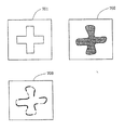
従来処理の概略フローと処理に使われる画像例を図1.と図7.に示す。初めに、101で設計データから求めたいパターンのテンプレート登録を行う。設計データから登録されたパターンを701に示す。次に102でSEM画像を取得する。取得されたSEM画像を702に示す。103で取得したSEM画像にソーベルフィルタ等のエッジ強調フィルタを施す。104でエッジが強調された画像を2値化してエッジだけが抽出された線画像にする。703に702のSEM画像から抽出された線画像を示す。105では101で登録された設計データと正規化相関等のマッチング処理を行う。
【0005】
【発明が解決しようとする課題】
従来の半導体検査システムでは、画像認識のためのポイントや測長位置及び測長アルゴリズムの登録は、実際のウェハを一度撮影してみて、それを用いて行っていた。そのため、登録のための時間がかかることとその時間装置を占有することからスループットが向上しないという問題があった。また、実際のSEM画像を見て人が判断し登録するため必ず操作者が必要となりオペレータフリーな完全自動化された半導体検査システムが構築できないという問題があった。さらに、設計情報とSEM画像のマッチング技術においても従来の技術では、CADデータとSEM画像の形状変化に対応できないことや、SEM画像からエッジ情報を取り出す場合に画像のS/N(信号/雑音比)によりエッジ情報を充分に取り出せないことや、2値化により線画像を作る場合に閾値の決定が難しく最適な値を求められないことがあった。そのため、その後の正規化相関によるマッチング処理で、相関係数が非常に小さくなる問題があった。
【0006】
本発明の目的は、CADデータ等の設計情報から撮影の条件、測長するポイント、測長のアルゴリズムまで検査に必要な全ての条件を作成し、その条件で実際の検査を行うオペレータフリーな完全自動化された半導体検査システムを実現することとそのシステムにおいて設計データをテンプレートにしてSEM画像とのマッチング処理行う場合に、相関値が高く安定したマッチング処理を実行できる半導体検査システムを実現することにある。
【0007】
【課題を解決するための手段】
上記目的を達成するために、請求項1記載の発明は、半導体検査システムについて、CADデータ等の半導体チップの設計情報を格納し、前記設計情報に基づいて半導体ウェハの検査すべき領域を含む撮影/検査条件を設定するナビゲーションシステムと、設定された撮影/検査条件に従って実際に半導体ウェハの撮影を行い、検査を実行する走査型電子顕微鏡システムから構成されることを特徴とする。
【0008】
請求項2記載の発明は、請求項1記載の半導体検査システムにおいて、前記ナビゲーションシステムは、自ら半導体パターンの設計機能持つこと、もしくはネットワークで接続されている設計機能を持つ他のナビゲーションシステムから設計情報を受け取る機能を持つことを特徴とする。
【0009】
請求項3記載の発明は、請求項1記載の半導体検査システムにおいて、前記ナビゲーションシステムは、格納されている前記設計情報から、所望の設計データを指定して取り出し、表示画面上に表示することを特徴とする。
【0010】
請求項4記載の発明は、請求項1記載の半導体検査システムにおいて、前記ナビゲーションシステムは、格納されている前記設計情報であるCADデータから任意の部分を指定して取り出し、ビットマップデータを作成する機能を持つことを特徴とする。
【0011】
請求項5記載の発明は、請求項1記載のの半導体検査システムにおいて、ナビゲーションシステムは、走査型電子顕微鏡システムで使用する撮影/検査条件を全てCADデータを含む前記設計情報から自動的に編集でき、編集された撮影/検査条件を前記走査型電子顕微鏡装置へ送信する機能を持つことを特徴とする。
【0012】
請求項6記載の発明は、請求項1記載の半導体検査システムにおいて、ナビゲーションシステムは、設置施設のネットワークに接続されている他のナビゲーションシステムとデータの授受ができ、さらに前記ネットワークに接続されている複数の前記走査型電子顕微鏡システムへ撮影/検査条件を送信する機能を持つことを特徴とする。
【0013】
請求項7記載の発明は、請求項1記載の半導体検査システムにおいて、前記ナビゲーションシステムは、格納されている設計情報から所望の設計データを取り出し、ビットマップデータを作成する機能を有するビットマップデータ作成部とその設計データから走査型電子顕微鏡システムで使用する撮影/検査条件を編集し送信する機能を有する撮影/検索条件編集部を含んで構成されることを特徴とする。
【0014】
請求項8記載の発明は、請求項1記載の半導体検査システムにおいて、前記ナビゲーションシステムは、前記走査型電子顕微鏡システムで使用する検査条件の一つとして、ビットマップデータから位置決め用のテンプレート選択を行う場合、特徴のあるパターン部分を自動的に検出しテンプレートとして登録する機能を持つことを特徴とする。
【0015】
請求項9記載の発明は、請求項1記載の半導体検査システムにおいて、前記走査型電子顕微鏡システムは、前記ナビゲーションシステムから受信した撮影/検査条件を使い、自動的にSEM画像を取得し、検査を実行することを特徴とする。
【0016】
請求項10記載の発明は、請求項1記載の半導体検査システムにおいて、前記走査型電子顕微鏡システムは、ネットワークで接続されている他のナビゲーションシステムから受信した撮影/検査条件を使い、自動的にSEM画像を取得し、検査を実行することを特徴とする。
【0017】
請求項11記載の発明は、請求項1記載の半導体検査システムにおいて、前記走査型電子顕微鏡システムは、前記設計情報から作成したビットマップデータとSEM画像との間での位置決め(マッチング)機能を有することを特徴とする。
【0018】
請求項12記載の発明は、請求項11記載の半導体検査システムにおいて、走査型電子顕微鏡システムは、前記設計情報からのビットマップデータをテンプレートとして、SEM画像とのマッチング処理を行う際に、撮影により得られたSEM画像とビットマップデータであるテンプレートからそれぞれエッジ情報を取り出してエッジ画像を作成する手段とSEM画像及びテンプレートからそれぞれ作成したエッジ画像に対して、両方の画像にそれぞれ平滑化処理を施し、両者の形状変化分を補うようにしてマッチング処理を行う手段を有する事を特徴とする。
【0019】
請求項13記載の発明は、請求項11記載の半導体検査システムにおいて、前記走査型電子顕微鏡システムは、SEM画像とビットマップデータであるテンプレートからエッジ情報を取り出してエッジ画像を作成する場合、方向別にエッジ情報を取り出して、方向別のエッジ画像を作成し、それぞれの画像においてマッチング処理を行う事を特徴とする。
【0020】
請求項14記載の発明は、請求項11記載の半導体検査システムにおいて、前記走査型電子顕微鏡システムは、SEM画像とビットマップデータであるテンプレートからエッジ情報を取り出してエッジ画像を作成する場合、方向別に作成したエッジ画像を1枚の画像に合成して、マッチング処理を行う事を特徴とする。
【0021】
請求項15記載の発明は、請求項1記載の半導体検査システムにおいて、前記走査型電子顕微鏡システムは、前記設計情報からのビットマップデータをテンプレートとして、SEM画像とのマッチング処理を行う際に、撮影により得られたSEM画像からエッジ情報を取り出してエッジ画像を作成する手段とそのエッジ画像と設計データとのマッチング処理によって検出されたエッジ画像の位置に対応したSEM画像の部分をテンプレートとして再登録しなおす手段とそれ以後のマッチング処理において再登録したSEM画像のテンプレートを使用する手段を有する事を特徴とする。
【0022】
請求項16記載の発明は、請求項15記載の半導体検査システムにおいて、前記走査型電子顕微鏡システムは、再登録したSEM画像のテンプレートを使い、繰り返し撮影されたSEM画像に対してマッチング処理を行う場合に、繰り返し行われる撮影の任意の時間または処理回数間隔で、テンプレート再登録を実施する事を特徴とする。
【0023】
請求項17記載の発明は、請求項15記載の半導体検査システムにおいて、新たにテンプレート再登録を行う場合に、設計データとSEM画像との相関値を比較し、今までのものより大きい場合にのみ、テンプレート再登録を行う事を特徴とする。
【0024】
請求項18記載の発明は、請求項15記載の半導体検査システムにおいて、初めの任意数回だけ、マッチング処理を行い、その時の相関値を比較し、その内の一番大きなものに対して、テンプレート再登録を行う事を特徴とする。
【0025】
請求項19記載の発明は、請求項1記載の半導体検査システムにおいて、撮影/検査の条件は、前記ナビゲーションシステムもしくは前記走査型電子顕微鏡システムのどちらかに事前に登録してある撮影/検査条件ファイルから選択することを特徴とする。
【0026】
請求項20記載の発明は、請求項19記載の半導体検査システムにおいて、前記撮影/検査条件ファイルから選択する場合に、過去の使用頻度によって重み付けされ選択されることを特徴とする。
【0027】
請求項21記載の発明は、請求項19記載の半導体検査システムにおいて、前記撮影/検査条件ファイル内にある撮影/検査条件は、使用頻度が規定頻度より少ない場合に撮影/検査条件ファイルから自動的に削除されることを特徴とする。
【0028】
請求項22記載の発明は、請求項19記載の半導体検査システムにおいて、事前に登録してある撮影/検査条件ファイル内にある撮影/検査条件の一部を変更、編集する機能を有することを特徴とする。
【0029】
請求項23記載の発明は、請求項19記載の半導体検査システムにおいて、事前に登録してある撮影/検査条件ファイル内にある撮影/検査条件の一部を変更した場合、その条件を撮影/検査条件ファイル内に別の条件として登録する機能を有することを特徴とする。
【0030】
請求項1にかかる半導体検査システムでは、半導体チップの設計データを格納したナビゲーションシステムと、その情報を使って実際に半導体ウェハの撮影/検査を実行する走査型電子顕微鏡システムから構成されており、半導体チップの設計データを用いて撮影/検査の条件を作成し、それを実際に実行するシステムを構築できる。
【0031】
請求項2にかかる半導体検査システムでは、ナビゲーションシステムは、自ら設計機能を持つか、またはネットワークで接続されている他の設計機能を持つシステムから設計情報を受け取り格納する機能を持つので、これらの設計情報に基づいて撮影/検査の条件を容易に設定できる。
【0032】
請求項3にかかる半導体検査システムでは、ナビゲーションシステムに対して、パターン設計に必要なレイヤ、セル等の各情報が格納されている設計情報の内、所望の設計データを取り出し、表示画面上に表示す機能を持たせたため、操作者がそれをもとに撮影/検査の条件を能率良く設定できる。
【0033】
請求項4にかかる半導体検査システムでは、ナビゲーションシステムに対して、設計情報であるCADデータから任意の指定された部分を取り出してビットマップデータを作成する機能を持たせたため、走査型電子顕微鏡システムでのマッチングにそのデータが使用できる。
【0034】
請求項5にかかる半導体検査システムでは、ナビゲーションシステムに対して、走査型電子顕微鏡システムで使用する撮影/検査条件を全てCADデータを含む設計情報から自動的に編集でき、その条件を走査型電子顕微鏡システムへ送信する機能を持たせたため、走査型電子顕微鏡システムでは自動的に抽出された条件を使って、撮影/検査が実行でき、システムの全自動化が可能になる。
【0035】
請求項6にかかる半導体検査システムでは、ナビゲーションシステムに対して、設置施設のネットワークと接続させ他のナビゲーションシステムとデータの授受できるようにし、さらにネットワークに接続されている複数の走査型電子顕微鏡システムへ撮影/検査条件を送信する機能を持たせたため、複数のナビゲーションシステム及び複数の走査型電子顕微鏡システムと協働して効率的な撮影/検査を実行できる。
【0036】
請求項7にかかる半導体検査システムでは、ナビゲーションシステムは、格納されている設計情報から所望の設計データを取り出し、ビットマップデータを作成する機能を有する部分とその設計データから走査型電子顕微鏡システムで使用する撮影/検査条件を編集し送信する機能を有する部分を含んで構成されるため、ビットマップデータを用いた撮影/検索条件の編集が可能であり、また、ネットワークを利用してナビゲーションシステムを複数のシステムから構成することもできる。
【0037】
請求項8にかかる半導体検査システムでは、ナビゲーションシステムに対して、走査型電子顕微鏡システムで使用する検査条件の一つとして、ビットマップデータから位置決め用のテンプレート選択を行う場合、特徴のあるパターン部分を自動的に検出しテンプレートとして登録する機能を持たせたため、テンプレート登録に人手を用いる必要がない。
【0038】
請求項9にかかる半導体検査システムでは、走査型電子顕微鏡システムに対して、ナビゲーションシステムから受信した撮影/検査条件を使い、自動的にSEM画像を取得し、検査を実行する機能を持たせたため、操作者によるコントロールが不要で、撮影/検査の自動化が可能である。
【0039】
請求項10にかかる半導体検査システムでは、走査型電子顕微鏡システムに対して、ネットワークで接続されている他のナビゲーションシステムから受信した撮影/検査条件を使い、自動的にSEM画像を取得し、検査を実行する機能を持たせたため、複数の走査型電子顕微鏡システムを操作者のコントロールなしで自動的に稼動できる。
【0040】
請求項11にかかる半導体検査システムでは、走査型電子顕微鏡システムに対して、設計データから作成したビットマップデータとSEM画像との間での位置決め(マッチング)機能を持たせたため、走査型電子顕微鏡システムで設計情報を利用した精度が高く効率的な検査が行える。
【0041】
請求項12にかかる半導体検査システムでは、走査型電子顕微鏡システムに対して、設計データからのビットマップデータとSEM画像とのマッチング処理を行う際に、それぞれの画像からエッジ情報を取り出してエッジ画像を作成し、さらにそれぞれ平滑化処理を施し、両者の形状変化分を補うようにしてマッチング処理を行う機能を持たせたため、検出率の良いマッチングが行える。
【0042】
請求項13にかかる半導体検査システムでは、走査型電子顕微鏡システムに対して、SEM画像とビットマップデータからエッジ情報を取り出してエッジ画像を作成する場合、方向別にエッジ情報を取り出して、方向別のエッジ画像を作成し、それぞれの画像においてマッチング処理を行う機能を持たせたため、位置精度の良いマッチングが行える。
【0043】
請求項14にかかる半導体検査システムでは、走査型電子顕微鏡システムに対して、SEM画像とビットマップデータからエッジ情報を取り出してエッジ画像を作成する場合、方向別に作成したエッジ画像を1枚の画像に合成して、マッチング処理を行う手段を持たせたため、位置精度が良くマッチングを高速に行うことができる。
【0044】
請求項15にかかる半導体検査システムでは、再登録したSEM画像のテンプレートを使用するので、SEMの濃淡画像同士のマッチング処理となるため、相関値を高く、検出率も安定したマッチング処理を行う事ができる。
【0045】
請求項16にかかる画像処理装置では、繰り返し行われる撮影の任意の時間または処理回数間隔で、請求項15記載のテンプレート再登録を行うので、撮影途中でのSEM画像の経時的変化に対しても、相関値を高く、検出率も安定したマッチング処理を行う事ができる。
【0046】
請求項17にかかる画像処理装置では、新たにテンプレート再登録を行う場合に、設計データとSEM画像との相関値を比較し、今までのものより大きい場合にのみ、テンプレート再登録を行うので、相関値が高いテンプレートに最適化を行うことができる。
【0047】
請求項18にかかる画像処理装置では、初めの任意数回だけ、請求項15記載の設計データとエッジ画像のマッチング処理を行い、その時の相関値を比較し、その内の一番大きなものに対して、テンプレート再登録を行うので、相関値が高いSEM画像のテンプレートを選択できる。
【0048】
請求項19にかかる半導体検査システムでは、ナビゲーションシステムもしくは走査型電子顕微鏡システムのどちらかに対して、撮影/検査の条件を事前に登録してあるファイルから選択する機能を持たせたため、効率よく条件を決定できる。
【0049】
請求項20にかかる半導体検査システムでは、撮影/検査条件ファイルから選択する場合に、過去の使用頻度によって重み付けして選択することで効率よく条件を決定できる。
【0050】
請求項21にかかる半導体検査システムでは、撮影/検査条件ファイル内にある撮影/検査条件は、使用頻度が規定頻度より少ない場合に撮影/検査条件ファイルから自動的に削除されるので効率よく条件を決定できる。
【0051】
請求項22にかかる半導体検査システムでは、前記第19項の半導体検査システムに対して、事前に登録してある撮影/検査条件ファイル内にある撮影/検査条件の一部を変更、編集する機能を持たせたため、以前の条件を参考にしながら効率よく条件を決定できる。
【0052】
請求項23にかかる半導体検査システムでは、前記第19項の半導体検査システムに対して、事前に登録してある撮影/検査条件ファイル内にある撮影/検査条件の一部を変更した場合、その条件を撮影/検査条件ファイル内に別の条件として登録する機能を持たせたため、その後の条件決定時に効率が良い。
【0053】
【発明の実施の形態】
図3は、本発明の走査型電子顕微鏡システムの構成概要のブロック図である。301は電子顕微鏡の鏡体部であり、電子銃302から発せられた電子線303が図には描かれていない電子レンズによって収束され、試料305に照射される。電子線照射によって、試料表面から発生する二次電子、或いは反射電子の強度が電子検出器306によって検出され、増幅器307で増幅される。304は電子線の位置を移動させる偏向器であり、制御用計算機310の制御信号308によって電子線303を試料表面上でラスタ走査させる。増幅器307から出力される信号を画像処理プロセッサ309内でAD変換し、デジタル画像データを作る。311は、その画像データを表示する表示装置である。また、画像処理プロセッサ309は、デジタル画像データを格納する画像メモリと各種の画像処理を行う画像処理回路、表示制御を行う表示制御回路を持つ。制御用計算機310には、キーボードやマウス等の入力手段312が接続される。
【0054】
半導体デバイス作成時、ウェハ上に描かれた微細なパターンの線幅を計測する場合に電子顕微鏡装置が使われる。この時、ウェハ上の線幅を計測する部分を見つけ出す方法として、現在では、正規化相関法が使われており、その場合に最適なテンプレート選択が必要とされている。本発明の画像処理プロセッサ309は、テンプレートマッチングにおけるテンプレート選択を最適に行うことができるよう構成されているため、電子顕微鏡装置に適応することが可能である。
【0055】
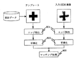
図2は、本発明の一実施例である設計データとSEM画像を使ったマッチング処理フローである。初めに201で設計データから検出したいパターン部分をテンプレート登録する。202でSEM画像を取得し、203でマッチング処理を行う。このマッチング処理に関しては、いろいろな手法があるが、例えば図1の103〜105と同様な手法(エッジ強調フィルタ処理、2値化処理、正規化相関処理)を用いれば良い。その結果、設計データのパターンと相対応したSEM画像上位置が204で検出される。次に205で、204で検出された位置に対応したSEM画像の部分をテンプレートとして再登録する。その後、206でSEM画像を取得し、205で再登録したSEM画像をテンプレートとしてマッチング処理を行い、208で位置検出を行う。こうすることで、再登録したテンプレートがSEM画像であるので、SEMの濃淡画像同士のマッチング処理となるため、相関値を高く、検出率も安定したマッチング処理を行う事が可能になる。複数の検出を行う場合は、206から209までの過程を繰り返すことになる。なお、最初に登録するテンプレートを予め設定しておけば、その後の処理はコンピュータプログラムにより自動的に進行させられる。
【0056】
図4は、本発明の一実施例である経時的にテンプレートとしてSEM画像を再登録する場合の処理フローである。401から408は図2の201から208に対応する。409で一定の時間間隔または処理回数間隔でテンプレート再登録を行うか行わないかの判定を行い、行う場合は、再度、設計データとSEM画像を使ったマッチング処理を行うため、402から405の工程を実行する。こうすることで、撮影途中でのSEM画像が経時変化しても、相関値を高く、検出率も安定したマッチング処理を行う事ができる。
【0057】
図5は、本発明の一実施例である前回の相関値より大きい相関値が得られた場合にテンプレートとしてSEM画像を再登録する場合の処理フローである。501から504と506から510は図4の401から404と405から409に対応する。510で一定の時間間隔または処理回数間隔でテンプレート再登録を行うか行わないかの判定を行い、行う場合は、再度、設計データとSEM画像を使ったマッチング処理を行うため、502から504の工程を実行する。次に505で今回検出された位置の相関値が前回までのテンプレートの相関値より大きい場合は、506のテンプレート再登録を行うが、小さい場合は、再登録を行わず、507からの処理に入る。したがって、使用するテンプレートを相関値が最も高いテンプレートに最適化を行うことができる。
【0058】
図6は、本発明の一実施例である任意回数、設計データとSEM画像とのマッチング処理を行い、その内、相関値が最も高い位置のSEM画像をテンプレートとして再登録する場合の処理フローである。601から604と606から610は図2の201から204と205から209に対応する。602から605まで任意回数、設計データとSEM画像を使ったマッチング処理を繰返し、606で、検出された位置の内で相関値が最も高い位置のSEM画像をテンプレートとして再登録する。そのため、相関値が高いSEM画像のテンプレートを選択できる。複数の検出を行う場合は、そのテンプレートを使い、607から609までの過程を繰り返すことになる。なお、図4から図6の処理もコンピュータプログラムによる自動化が可能である。
【0059】
図8は、本発明の一実施例であるビットマップデータのテンプレートとSEM画像とのマッチング処理の処理フローである。801でビットマップデータとSEM画像、それぞれからエッジ情報を抽出する。この部分の処理には、一般的にはソーベルフィルタ等のエッジ強調フィルタが用いられる。この部分で両画像は、コントラスト情報が失われマッチングがしやすくなるが、SEM画像は実際のCADデータとはかなり形状が異なっているため、このままではマッチングの検出率が低いものになってしまう。そこで、802でエッジ画像となった両画像に対して平滑化処理を施して両者の形状変化を補う。この部分の処理には、やや強めの平滑フィルタを施す。また、CADデータとSEM画像の平滑化の強度を変え、CADデータの平滑化をより強めに行う必要がある。このように、形状変形部分を補正したエッジ画像同士を803でマッチング処理するため検出率の高いマッチング処理が行える。なお、最初に抽出するビットマップデータとSEM画像、それぞれからエッジ情報を予め設定しておけば、コンピュータプログラムによるマッチング処理の自動化が可能である。
【0060】
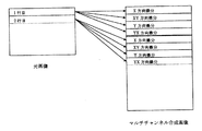
図9は、本発明の別の実施例であるビットマップデータのテンプレートとSEM画像とのマッチング処理の処理フローである。図8の処理フローと異なる点は、901でのエッジ抽出を方向別に行う点である。方向別のエッジ抽出処理には、一般的に方向別のエッジを抽出ができるソーベルフィルタを用いる。方向は、X,Yの2方向もしくはX,Y,XY,YXの4方向を用いる。902では、形状変化部分を補うための平滑化処理を各方向に分解されたエッジ画像それぞれに対して行う。903では、各方向に分割された画像を図10のように合成統合する。このように合成することで903では1枚の画像同士のマッチングとして処理を行うことができる。もちろん、903の統合を行わず、それぞれの方向同士を別々にマッチング処理させることもできる。このように方向別にエッジを抽出しマッチング処理させることで、各方向のマッチング精度を向上させることができる。なお、図10の元画像は図9のテンプレート及び入力SEM画像に対応しており、これらの画像のX方向微分を求めるときには、元画像をY方向に複数行に分割して行う。また、Y方向微分を求めるときには、元画像をX方向に複数行に分割して行う。このマッチング処理についてもコンピュータプログラムによる自動化が可能である。
【0061】
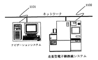
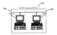
図11は、本発明の一実施例である半導体検査システムの構成図である。1101がCADデータ等の半導体チップの設計情報を格納し、その設計情報内から検査すべき領域を任意に取り出すことのできるナビゲーションシステムである。1102がその情報を使って実際に半導体ウェハの撮影を行い、所定の検査を実行する走査型電子顕微鏡システムである。これらのシステム1101と1102はネットワークで繋がっており、情報やデータをやり取りできる構成になっている。
【0062】
図12は、本発明の一実施例であるナビゲーションシステムの構成図である。ナビゲーションシステム1101は、格納されている設計情報から所望の設計データを取り出し、ビットマップデータを作成する機能を有するビットマップデータ作成部1201とその設計データから走査型電子顕微鏡システム1102で使用する撮影/検査条件を編集し送信する機能を有する撮影/検査条件編集部1202から構成される。また、ナビゲーションシステム1101は、1台のWS(ワークステーション)もしくはPC(パーソナルコンピュータ)内にビットマップデータ作成部1201と撮影/検査条件編集部1202の機能部分を分割し構成しても良いし、2台もしくは複数のWSもしくはPCに機能を分割して構成しても良い。
【0063】
図13は、本発明の一実施例である半導体検査システムの構成図である。1302のナビゲーションシステムは、自ら半導体パターンの設計機能を持ち、設計機能を持たない場合は、ネットワークを介して接続されていて設計機能を持つ他のシステム1301から設計情報を受け取り、その情報を用いる。
【0064】
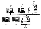
図14は、本発明の一実施例である半導体検査システムのネットワーク構成図である。本発明の半導体検査システムにおいては、ナビゲーションシステム1401は、設置施設のネットワークに接続されている他のナビゲーションシステム1402〜1404とデータの授受ができ、さらにネットワークに接続されている複数の走査型電子顕微鏡システム1405〜1406へ撮影/検査条件を送信するできる。こうすることで撮影/検査条件の共有化ができると伴に複数のシステムを同時に自動運転することができる。
【0065】
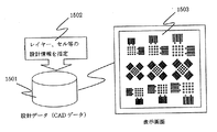
図15は、本発明の一実施例であるナビゲーションシステムでの表示例である。ナビゲーションシステムには、半導体の設計データ1501が格納されていて、操作者が1502のレイヤ、セル等の設計情報を指定入力することで、その設計データ1501から指定部分1502を取り出し、1503のように表示画面上に表示する機能を持つ。この場合、1501は、図13のようにネットワークで繋がった設計システム上にあってもよい。
【0066】
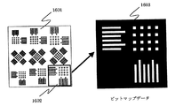
図16は、本発明の一実施例であるナビゲーションシステム1302で作成されるビットマップデータ例である。1601が図15で設計データから取り出された領域であり、この領域内から1602のような検査/測長する部分を指定する。この場合、検査/測長指定領域1602は1603のようなビットマップデータに変換され、走査型電子顕微鏡システム1303へ送られる。ここでは、ビットマップデータ1603として白黒2値を用いているが、この色は任意に設定することができる。
【0067】
図17は、本発明の一実施例であるナビゲーションシステムで行われる処理フローである。1701で、図15に示したように、設計のレイヤ、セル情報等を指定し、格納されている設計データから指定されたデータを画面上に表示する。1702は撮影領域の指定であり、1703で視野内(撮影領域として指定された領域)のパターンデータと位置情報を取り込み、ビットマップデータ1603に変換する。この部分は図16に示した内容と同じである。次に1704で検査/測長する箇所を指定し、その座標データを読み込み、1705で位置決め用のテンプレートの指定を行う。テンプレートの指定は、通常最も特異性の強い特徴のある部分を操作者が選んで指定するが、このような特徴のある部分は画像の高周波成分や特異性を評価する画像処理技術を用いて自動指定することも可能である。最後に1706で、1701から1705の情報に基づいて走査型電子顕微鏡システムで撮影/検査を行うために必要な全ての情報を編集し、操作型電子顕微鏡システムへ送信する。
【0068】
図18は、本発明の一実施例であるナビゲーションシステムにおける測長点とテンプレートの指定例である。1801が測長点の指定であり、1802がテンプレートの指定である。ここで指定対象の画像をビットマップデータとしたが、もちろんビットマップデータ変換前の設計データ上で指定しても構わない。
【0069】
図19は、本発明の一実施例である走査型電子顕微鏡システムで行われる処理フローである。1901から1904においては、図17の1706から送られた情報からウェハアライメント情報、位置決め用のテンプレート情報、測長点情報、及び撮影条件と測長方法の登録を行う。1905で実際の撮影を行い、1906で1902で登録されたテンプレートを使ったサーチ処理(位置検出)を実行する。1907では1906で検出した位置決め座標から測長点を算出し測長を実行する。1908は全測長点に対して測長が終了したか否かの判定で、全測長点に対して測長を行うためである。
【0070】
図20は、本発明の一実施例である撮影/検査条件を登録した自動条件ファイルである。自動条件ファイルはナビゲーションシステムもしくは走査型電子顕微鏡システムのどちらあっても良い。自動条件ファイル2001に登録されている条件に従って走査型電子顕微鏡システムで実際の撮影/検査が行われる。ナビゲーションシステムで得られた情報から撮影/検査条件を決定する場合に本発明のように事前に登録されてあるレシピの中から最も適した条件を選択するようにすれば、条件作成処理を簡略化でき、管理やメンテナンスにおいても便利である。また、自動条件ファイルに登録されている各レシピは、2002のように一部変更、削除が可能であり、また別の名前で登録することも可能である。さらに、各レシピがどの程度使用されているか統計をとり、使用頻度の少ないレシピは自動的に削除していくことも可能である。
【0071】
図21は、本発明の一実施例である自動条件ファイルを使った場合の処理フローである。2101でレシピを新規作成すべきか否かを判断する。既に同一か一部修正可能なレシピが自動条件ファイル2001に存在していなければ、2102で新規に作成する。作成したら、2106で自動条件ファイル2001に新規レシピを登録する。登録後は当該レシピを参照して、2108で実行することが可能である。登録せずに実行のみ行うこともある。同一か一部修正可能なレシピが自動条件ファイル2001に既に存在している場合は、2103で自動条件ファイル内にある既存のレシピを参照して、2104で一部変更をすべきか否かを判断する。同一であれば一部変更の必要はなく、2108でそのまま既存のレシピを実行する。また、同一でなくても既存レシピで代用可能であれば同様である。一部変更する場合は、2105で一部変更の後に、2106で自動条件ファイル2001に変更したレシピを登録すべきか否かの判断を行い、2107、2008で登録して実行するか、登録せず2108で実行する。このフローに従い一度使ったレシピを自動条件ファイルに登録することで、次回その条件を参照にすることが可能になる。また、撮影/検査条件の一部を変更した場合、2106で、その条件を別の条件として登録することも可能であり、この場合は変更前、変更後どちらのファイルも参照可能となる。
【0072】
【発明の効果】
本発明は、以上説明してきたように構成されているので以下に記載されるような効果を奏する。
【0073】
従来の半導体検査システムでは、画像認識のためのポイントや測長位置及び測長アルゴリズムの登録は、実際のウェハを一度撮影してみて、それを用いて行っていた。そのため、登録のための時間がかかることとその時間装置を占有することからスループットが向上しないという問題があった。また、実際のSEM画像を見て人が判断し登録するため必ず操作者が必要となりオペレータフリーな完全自動化された半導体検査システムが構築できないという問題があった。
【0074】
これらの問題に対し、本発明は、CADデータ等の設計情報から撮影の条件、測長するポイント、測長のアルゴリズムまで検査に必要な全ての条件を作成し、その条件で実際の検査を行うので、オペレータフリーな完全自動化された高スループットな半導体検査システムを実現することができる。
【0075】
また、従来、設計データとSEM画像のマッチング処理を行う場合、設計データとSEM画像の形状変化分が対策できずに相関係数が非常に小さくなり、安定したマッチング処理を行うことができなかった。この問題に対し、本発明は設計データとSEM画像のマッチング処理を行う場合に方向別のエッジ情報とその平滑化により形状変化分を補うマッチング処理を行う。また本発明は、エッジ画像と設計データのテンプレートとの間でマッチング処理を行い、検出された位置に対応したSEM画像の部分をテンプレートとして再登録しなおしマッチング処理を行うため、相関値が高く、検出率も安定したマッチング処理を実現することができる。
【図面の簡単な説明】
【図1】従来の設計データとSEM画像のマッチング処理フロー
【図2】本発明の一実施例である設計データとSEM画像を使ったマッチング処理フロー
【図3】本発明の画像処理装置の一実施例である半導体検査システムの構成概要
【図4】本発明の一実施例である経時的にテンプレートとしてSEM画像を再登録する場合の処理フロー
【図5】本発明の一実施例である前回の相関値より高い場合にテンプレートとしてSEM画像を再登録する処理フロー
【図6】本発明の一実施例である任意回数の設計データとSEM画像とのマッチング処理の内で相関値が最も高い位置のSEM画像をテンプレートとして再登録する処理フロー
【図7】従来の処理に使われる画像例
【図8】本発明の一実施例であるビットマップデータのテンプレートとSEM画像とのマッチング処理の処理フロー
【図9】本発明の別の実施例であるビットマップデータのテンプレートとSEM画像とのマッチング処理の処理フロー
【図10】各方向に分割された画像の合成統合方法
【図11】本発明の一実施例である半導体検査システムの構成図
【図12】本発明の一実施例であるナビゲーションシステムの構成図
【図13】本発明の一実施例である半導体検査システムの構成図
【図14】本発明の一実施例である半導体検査システムのネットワーク構成図
【図15】本発明の一実施例であるナビゲーションシステムでの表示例
【図16】本発明の一実施であるナビゲーションシステムで作成されるビットマップデータ例
【図17】本発明の一実施例であるナビゲーションシステムで行われる処理フロー
【図18】本発明の一実施例であるナビゲーションシステムにおける測長点とテンプレートの指定例
【図19】本発明の一実施例である走査型電子顕微鏡システムで行われる処理フロー
【図20】本発明の一実施例である撮影/検査条件を登録した自動条件ファイル
【図21】本発明の一実施例である自動条件ファイルを使った場合の処理フロー
【符号の説明】
1101・・・ナビゲーションシステム、1102・・・走査型電子顕微鏡システム[0001]
[Industrial application fields]
The present invention relates to a semiconductor inspection system for analyzing a pattern on a semiconductor wafer using design data, and more particularly to a system configuration, design data, and SEM (scanning type) for automatically generating pattern imaging / inspection conditions from design data. It is related with the semiconductor inspection system provided with the method of performing matching processing with an image stably.
[0002]
[Prior art]
In recent years, the semiconductor industry has shifted from memory production to system LSI (abbreviation for Large Scale Integrated Circuit) production. When viewed as a pattern on a semiconductor wafer, the pattern of the system LSI is not created as a simple repetitive pattern, unlike the pattern of the memory. Therefore, when measuring a pattern of a system LSI with a length measuring SEM which is one of semiconductor evaluation apparatuses, it is necessary to frequently change a measurement position, that is, a matching template. Pre-design data such as CAD (Computer Aided Design) is used because taking images for template registration frequently during actual measurement significantly reduces the overall throughput. It is desirable to generate a template directly from In addition, since the wafer size is 300mm and it can no longer be transported by hand, and inspection in a high-purity clean room is becoming necessary, it is desired that the semiconductor factory be completely robotized. . Therefore, not only the template for positioning, but also all the conditions necessary for inspection, from design information to shooting conditions, points to measure, and length measurement algorithms, and operator-free to perform actual inspection under those conditions There is a need for a fully automated semiconductor inspection system.
[0003]
In the conventional length measurement SEM, registration of the point for image recognition, the length measurement position, and the length measurement algorithm is performed by photographing an actual wafer once and using it. In other words, an actual wafer is required, and the length measuring SEM must be temporarily occupied in order to take an SEM image and register various conditions. Moreover, the matching technology between the design data and the SEM image is not sufficient, and the matching cannot be performed with high accuracy. For example, when design data is used as a template in the prior art to specify the pattern position on a SEM image of a semiconductor wafer, the edge image is detected by filtering the SEM image using a Sobel filter or the like to detect edge components. It was created and matching was performed between the edge image and the design data, such as normalized correlation processing.
[0004]
Fig. 1 shows an outline flow of conventional processing and an image example used for processing. And FIG. Shown in First, in 101, a template of a pattern desired to be obtained from design data is registered. A
[0005]
[Problems to be solved by the invention]
In the conventional semiconductor inspection system, registration of the point for image recognition, the measurement position, and the measurement algorithm is performed by photographing an actual wafer once and using it. For this reason, there is a problem that throughput is not improved because it takes time for registration and occupies the time device. In addition, there is a problem in that an operator is always required for a person to judge and register by looking at an actual SEM image, and an operator-free fully automated semiconductor inspection system cannot be constructed. Furthermore, in the matching technology between design information and SEM image, the conventional technology cannot cope with changes in the shape of CAD data and SEM image, and the S / N (signal / noise ratio) of image when extracting edge information from SEM image. ) Cannot sufficiently extract edge information, and when a line image is created by binarization, it is difficult to determine a threshold value, and an optimal value may not be obtained. Therefore, there has been a problem that the correlation coefficient becomes very small in the subsequent matching processing by normalized correlation.
[0006]
The purpose of the present invention is to create all conditions necessary for inspection from design information such as CAD data to shooting conditions, points to measure, length measurement algorithms, and operator-free complete inspection that performs actual inspections under those conditions. To realize an automated semiconductor inspection system and to realize a semiconductor inspection system that can execute a stable matching process with a high correlation value when matching processing with an SEM image using design data as a template in the system. .
[0007]
[Means for Solving the Problems]
In order to achieve the above object, according to a first aspect of the present invention, there is provided a semiconductor inspection system that stores design information of a semiconductor chip such as CAD data and includes an area to be inspected of a semiconductor wafer based on the design information. A navigation system for setting inspection conditions, and a scanning electron microscope system for actually inspecting a semiconductor wafer in accordance with the set imaging / inspection conditions and executing the inspection.
[0008]
According to a second aspect of the present invention, in the semiconductor inspection system according to the first aspect, the navigation system has its own design function for semiconductor patterns or design information from another navigation system having a design function connected via a network. It has the function to receive
[0009]
According to a third aspect of the present invention, in the semiconductor inspection system according to the first aspect, the navigation system specifies and extracts desired design data from the stored design information, and displays the design data on a display screen. Features.
[0010]
According to a fourth aspect of the present invention, in the semiconductor inspection system according to the first aspect, the navigation system designates and extracts an arbitrary part from CAD data which is the stored design information, and creates bitmap data. It is characterized by having a function.
[0011]
According to a fifth aspect of the present invention, in the semiconductor inspection system according to the first aspect, the navigation system can automatically edit all the photographing / inspection conditions used in the scanning electron microscope system from the design information including CAD data. The apparatus has a function of transmitting the edited imaging / inspection condition to the scanning electron microscope apparatus.
[0012]
According to a sixth aspect of the present invention, in the semiconductor inspection system according to the first aspect, the navigation system can exchange data with another navigation system connected to the network of the installation facility, and is further connected to the network. It has a function of transmitting imaging / inspection conditions to a plurality of the scanning electron microscope systems.
[0013]
A seventh aspect of the present invention is the semiconductor inspection system according to the first aspect, wherein the navigation system has a function of extracting desired design data from stored design information and generating bitmap data. And an imaging / search condition editing unit having a function of editing and transmitting imaging / inspection conditions used in the scanning electron microscope system from the design data.
[0014]
According to an eighth aspect of the present invention, in the semiconductor inspection system according to the first aspect, the navigation system selects a template for positioning from bitmap data as one of the inspection conditions used in the scanning electron microscope system. In this case, it has a function of automatically detecting a characteristic pattern portion and registering it as a template.
[0015]
According to a ninth aspect of the present invention, in the semiconductor inspection system according to the first aspect, the scanning electron microscope system automatically acquires an SEM image using an imaging / inspection condition received from the navigation system, and performs an inspection. It is characterized by performing.
[0016]
According to a tenth aspect of the present invention, in the semiconductor inspection system according to the first aspect, the scanning electron microscope system automatically uses an imaging / inspection condition received from another navigation system connected by a network to automatically perform an SEM. An image is acquired and an inspection is performed.
[0017]
The invention according to claim 11 is the semiconductor inspection system according to
[0018]
According to a twelfth aspect of the present invention, in the semiconductor inspection system according to the eleventh aspect, when the scanning electron microscope system performs the matching process with the SEM image using the bitmap data from the design information as a template, by photographing. Both the obtained SEM image and the template that is bitmap data are used to extract edge information to create an edge image, and the edge image created from each SEM image and template is subjected to smoothing processing on both images. , And a means for performing a matching process so as to compensate for the shape change between the two.
[0019]
According to a thirteenth aspect of the present invention, in the semiconductor inspection system according to the eleventh aspect, when the scanning electron microscope system extracts edge information from a template that is an SEM image and bitmap data, It is characterized in that edge information is extracted, edge images for each direction are created, and matching processing is performed on each image.
[0020]
According to a fourteenth aspect of the present invention, in the semiconductor inspection system according to the eleventh aspect, when the scanning electron microscope system extracts edge information from a template that is an SEM image and bitmap data, The created edge image is synthesized into a single image, and matching processing is performed.
[0021]
According to a fifteenth aspect of the present invention, in the semiconductor inspection system according to the first aspect, when the scanning electron microscope system performs a matching process with an SEM image using the bitmap data from the design information as a template. The edge information is extracted from the SEM image obtained by the above and the part of the SEM image corresponding to the position of the edge image detected by the matching process between the edge image and the design data is re-registered as a template. The present invention is characterized by having means for correcting and a means for using the template of the SEM image re-registered in the subsequent matching processing.
[0022]
According to a sixteenth aspect of the present invention, in the semiconductor inspection system according to the fifteenth aspect, the scanning electron microscope system uses a re-registered SEM image template and performs matching processing on a repeatedly taken SEM image. In addition, the template re-registration is performed at an arbitrary time of repeated photographing or at an interval of processing times.
[0023]
In the semiconductor inspection system according to claim 17, in the semiconductor inspection system according to claim 15, when new template re-registration is performed, the correlation value between the design data and the SEM image is compared and only when it is larger than the previous one. The template is re-registered.
[0024]
The invention according to claim 18 is the semiconductor inspection system according to claim 15, wherein the matching process is performed only for the first arbitrary number of times, the correlation values at that time are compared, and the template of the largest one is compared with the template. It is characterized by re-registration.
[0025]
According to a nineteenth aspect of the present invention, in the semiconductor inspection system according to the first aspect, the photographing / inspection condition file is a photographing / inspection condition file registered in advance in either the navigation system or the scanning electron microscope system. It is characterized by selecting from.
[0026]
According to a twentieth aspect of the present invention, in the semiconductor inspection system according to the nineteenth aspect, when selecting from the imaging / inspection condition file, the selection is weighted according to the past use frequency.
[0027]
According to a twenty-first aspect of the present invention, in the semiconductor inspection system according to the nineteenth aspect, the photographing / inspection conditions in the photographing / inspection condition file are automatically extracted from the photographing / inspection condition file when the use frequency is less than a prescribed frequency. It is deleted.
[0028]
According to a twenty-second aspect of the present invention, in the semiconductor inspection system according to the nineteenth aspect, there is provided a function of changing or editing a part of photographing / inspection conditions in a pre-registered photographing / inspection condition file. And
[0029]
According to a twenty-third aspect of the present invention, in the semiconductor inspection system according to the nineteenth aspect, when a part of the photographing / inspection condition in the photographing / inspection condition file registered in advance is changed, the condition is photographed / inspected. It has a function of registering as another condition in the condition file.
[0030]
The semiconductor inspection system according to
[0031]
In the semiconductor inspection system according to
[0032]
In the semiconductor inspection system according to
[0033]
In the semiconductor inspection system according to the fourth aspect of the present invention, the navigation system has a function of taking out any designated portion from CAD data as design information and creating bitmap data. The data can be used for matching.
[0034]
In the semiconductor inspection system according to the fifth aspect, the radiographing / inspection conditions used in the scanning electron microscope system can be automatically edited from the design information including CAD data with respect to the navigation system. Since the function of transmitting to the system is provided, the scanning electron microscope system can perform imaging / inspection using automatically extracted conditions, and the system can be fully automated.
[0035]
In the semiconductor inspection system according to
[0036]
In the semiconductor inspection system according to
[0037]
In the semiconductor inspection system according to
[0038]
In the semiconductor inspection system according to
[0039]
In the semiconductor inspection system according to the tenth aspect, the SEM image is automatically acquired for the scanning electron microscope system using the imaging / inspection conditions received from another navigation system connected via the network, and the inspection is performed. With the function to execute, multiple scanning electron microscope systems can be operated automatically without operator control.
[0040]
In the semiconductor inspection system according to the eleventh aspect, since the scanning electron microscope system has a positioning (matching) function between the bitmap data created from the design data and the SEM image, the scanning electron microscope system is provided. The design information can be used for highly accurate and efficient inspection.
[0041]
In the semiconductor inspection system according to claim 12, when performing the matching process between the bitmap data from the design data and the SEM image with respect to the scanning electron microscope system, the edge information is extracted from each image to obtain the edge image. Since a function of performing the matching process by adding the smoothing process and compensating for the shape change between the two is provided, matching with a high detection rate can be performed.
[0042]
In the semiconductor inspection system according to claim 13, when the edge information is extracted from the SEM image and the bitmap data with respect to the scanning electron microscope system, the edge information is extracted for each direction, and the edge for each direction is acquired. Since an image is created and a function for performing matching processing on each image is provided, matching with high positional accuracy can be performed.
[0043]
In the semiconductor inspection system according to claim 14, when edge information is created by extracting edge information from the SEM image and bitmap data for the scanning electron microscope system, the edge image created for each direction is combined into one image. Since the means for performing the matching processing is provided by combining, it is possible to perform matching at high speed with good positional accuracy.
[0044]
In the semiconductor inspection system according to the fifteenth aspect, since the re-registered SEM image template is used, matching processing between the SEM grayscale images is performed. Therefore, matching processing with a high correlation value and a stable detection rate may be performed. it can.
[0045]
In the image processing apparatus according to the sixteenth aspect, since the template re-registration according to the fifteenth aspect is performed at an arbitrary time of photographing that is repeatedly performed or at an interval of the number of processing times, the temporal change of the SEM image during the photographing is also prevented. The matching process can be performed with a high correlation value and a stable detection rate.
[0046]
In the image processing apparatus according to claim 17, when a template re-registration is newly performed, the correlation value between the design data and the SEM image is compared, and the template re-registration is performed only when it is larger than the previous one. Optimization can be performed on a template having a high correlation value.
[0047]
In the image processing apparatus according to claim 18, the design data according to claim 15 is matched with the edge image only for the first arbitrary number of times, the correlation values at that time are compared, and the largest one of them is compared. Since template re-registration is performed, a template of an SEM image having a high correlation value can be selected.
[0048]
In the semiconductor inspection system according to the nineteenth aspect, since either the navigation system or the scanning electron microscope system has a function of selecting a photographing / inspection condition from a pre-registered file, the condition is efficiently improved. Can be determined.
[0049]
In the semiconductor inspection system according to the twentieth aspect, when selecting from the imaging / inspection condition file, the condition can be determined efficiently by selecting it by weighting according to the past use frequency.
[0050]
In the semiconductor inspection system according to claim 21, since the photographing / inspection conditions in the photographing / inspection condition file are automatically deleted from the photographing / inspection condition file when the usage frequency is less than the prescribed frequency, the conditions are efficiently determined. Can be determined.
[0051]
The semiconductor inspection system according to claim 22 has a function of changing or editing a part of the photographing / inspection conditions in the photographing / inspection condition file registered in advance with respect to the semiconductor inspection system according to the nineteenth aspect. Because it has, it can be determined efficiently with reference to the previous conditions.
[0052]
In the semiconductor inspection system according to claim 23, when a part of photographing / inspection conditions in the photographing / inspection condition file registered in advance is changed with respect to the semiconductor inspection system according to the nineteenth aspect, the condition Is added as another condition in the imaging / inspection condition file.
[0053]
DETAILED DESCRIPTION OF THE INVENTION
FIG. 3 is a block diagram of a schematic configuration of the scanning electron microscope system of the present invention. Reference numeral 301 denotes a mirror body part of an electron microscope, and an electron beam 303 emitted from an
[0054]
An electron microscope apparatus is used to measure the line width of a fine pattern drawn on a wafer when creating a semiconductor device. At this time, the normalized correlation method is currently used as a method for finding a portion for measuring the line width on the wafer, and in this case, an optimal template selection is required. Since the image processor 309 of the present invention is configured to be able to optimally perform template selection in template matching, it can be applied to an electron microscope apparatus.
[0055]
FIG. 2 shows a matching processing flow using design data and an SEM image according to an embodiment of the present invention. First, in 201, a pattern portion to be detected from design data is registered as a template. An SEM image is acquired at 202 and matching processing is performed at 203. For this matching process, there are various techniques. For example, the same techniques (edge enhancement filter process, binarization process, normalized correlation process) as 103 to 105 in FIG. 1 may be used. As a result, a position on the SEM image corresponding to the design data pattern is detected at 204. Next, at 205, the part of the SEM image corresponding to the position detected at 204 is re-registered as a template. Thereafter, an SEM image is acquired at 206, matching processing is performed using the SEM image re-registered at 205 as a template, and position detection is performed at 208. By doing so, since the re-registered template is an SEM image, matching processing between SEM grayscale images is performed, so that matching processing with a high correlation value and a stable detection rate can be performed. When a plurality of detections are performed, the process from 206 to 209 is repeated. If a template to be registered first is set in advance, the subsequent processing is automatically advanced by a computer program.
[0056]
FIG. 4 is a processing flow for re-registering an SEM image as a template over time according to an embodiment of the present invention. 401 to 408 correspond to 201 to 208 in FIG. In
[0057]
FIG. 5 is a processing flow for re-registering an SEM image as a template when a correlation value larger than the previous correlation value is obtained according to an embodiment of the present invention.
[0058]
FIG. 6 is a processing flow in the case where the design data and the SEM image are matched any number of times according to an embodiment of the present invention, and the SEM image at the highest correlation value is re-registered as a template. is there.
[0059]
FIG. 8 is a processing flow of matching processing between a bitmap data template and an SEM image according to an embodiment of the present invention. In
[0060]
FIG. 9 is a processing flow of a matching process between a bitmap data template and an SEM image according to another embodiment of the present invention. A difference from the processing flow of FIG. 8 is that edge extraction in 901 is performed for each direction. The edge extraction process for each direction generally uses a Sobel filter that can extract edges for each direction. As directions, two directions of X and Y or four directions of X, Y, XY and YX are used. In 902, smoothing processing for compensating for the shape change portion is performed on each edge image decomposed in each direction. In 903, the images divided in each direction are combined and integrated as shown in FIG. By synthesizing in this way, in 903, processing can be performed as matching between one image. Of course, it is also possible to perform matching processing for each direction separately without performing the integration of 903. Thus, by extracting the edge for each direction and performing matching processing, the matching accuracy in each direction can be improved. Note that the original image in FIG. 10 corresponds to the template and the input SEM image in FIG. 9, and when obtaining the X-direction differentiation of these images, the original image is divided into a plurality of lines in the Y direction. Further, when obtaining the Y-direction differentiation, the original image is divided into a plurality of lines in the X direction. This matching process can also be automated by a computer program.
[0061]
FIG. 11 is a configuration diagram of a semiconductor inspection system according to an embodiment of the present invention.
[0062]
FIG. 12 is a configuration diagram of a navigation system according to an embodiment of the present invention. The
[0063]
FIG. 13 is a configuration diagram of a semiconductor inspection system according to an embodiment of the present invention. When the
[0064]
FIG. 14 is a network configuration diagram of a semiconductor inspection system according to an embodiment of the present invention. In the semiconductor inspection system of the present invention, the
[0065]
FIG. 15 is a display example in the navigation system according to one embodiment of the present invention. In the navigation system,
[0066]
FIG. 16 is an example of bitmap data created by the
[0067]
FIG. 17 is a processing flow performed in the navigation system according to one embodiment of the present invention. At 1701, as shown in FIG. 15, the design layer, cell information, etc. are designated, and the designated data from the stored design data is displayed on the screen.
[0068]
FIG. 18 is an example of specifying the measurement points and templates in the navigation system according to one embodiment of the present invention.
[0069]
FIG. 19 is a processing flow performed in the scanning electron microscope system according to one embodiment of the present invention. In
[0070]
FIG. 20 is an automatic condition file in which imaging / inspection conditions are registered according to an embodiment of the present invention. The automatic condition file may be either a navigation system or a scanning electron microscope system. Actual photographing / inspection is performed by the scanning electron microscope system according to the conditions registered in the
[0071]
FIG. 21 is a processing flow when an automatic condition file according to an embodiment of the present invention is used. In 2101, it is determined whether or not a new recipe should be created. If there is no recipe that can be already corrected or partially corrected in the
[0072]
【The invention's effect】
Since the present invention is configured as described above, the following effects can be obtained.
[0073]
In the conventional semiconductor inspection system, registration of the point for image recognition, the measurement position, and the measurement algorithm is performed by photographing an actual wafer once and using it. For this reason, there is a problem that throughput is not improved because it takes time for registration and occupies the time device. In addition, there is a problem in that an operator is always required for a person to judge and register by looking at an actual SEM image, and an operator-free fully automated semiconductor inspection system cannot be constructed.
[0074]
In response to these problems, the present invention creates all the conditions necessary for inspection from design information such as CAD data to shooting conditions, length measurement points, and length measurement algorithms, and performs actual inspection under those conditions. Therefore, an operator-free fully automated high-throughput semiconductor inspection system can be realized.
[0075]
Conventionally, when performing matching processing between design data and SEM images, the shape coefficient of the design data and SEM images cannot be dealt with, and the correlation coefficient becomes very small, making it impossible to perform stable matching processing. . In order to solve this problem, the present invention performs matching processing that compensates for shape change by edge information for each direction and its smoothing when matching processing between design data and SEM images. Further, the present invention performs a matching process between the edge image and the template of the design data, re-registers the part of the SEM image corresponding to the detected position as the template, and performs the matching process. Matching processing with a stable detection rate can be realized.
[Brief description of the drawings]
[Fig. 1] Conventional design data and SEM image matching process flow
FIG. 2 is a flowchart of a matching process using design data and an SEM image according to an embodiment of the present invention.
FIG. 3 is a configuration outline of a semiconductor inspection system which is an embodiment of an image processing apparatus of the present invention.
FIG. 4 is a processing flow when re-registering an SEM image as a template over time according to an embodiment of the present invention.
FIG. 5 is a processing flow for re-registering an SEM image as a template when the correlation value is higher than the previous correlation value according to an embodiment of the present invention.
FIG. 6 is a processing flow for re-registering, as a template, an SEM image at a position having the highest correlation value in an arbitrary number of times of design data and SEM image matching processing according to an embodiment of the present invention.
FIG. 7 is an example of an image used for conventional processing.
FIG. 8 is a flowchart of a matching process between a bitmap data template and an SEM image according to an embodiment of the present invention.
FIG. 9 is a flowchart of a matching process between a bitmap data template and an SEM image according to another embodiment of the present invention.
FIG. 10 is a method of combining and integrating images divided in each direction.
FIG. 11 is a configuration diagram of a semiconductor inspection system according to an embodiment of the present invention.
FIG. 12 is a configuration diagram of a navigation system according to an embodiment of the present invention.
FIG. 13 is a configuration diagram of a semiconductor inspection system according to an embodiment of the present invention.
FIG. 14 is a network configuration diagram of a semiconductor inspection system according to an embodiment of the present invention.
FIG. 15 is a display example of a navigation system according to an embodiment of the present invention.
FIG. 16 is an example of bitmap data created by the navigation system according to one embodiment of the present invention.
FIG. 17 is a processing flow performed in the navigation system according to one embodiment of the present invention.
FIG. 18 shows an example of specifying a measurement point and a template in the navigation system according to one embodiment of the present invention.
FIG. 19 is a processing flow performed in a scanning electron microscope system according to an embodiment of the present invention.
FIG. 20 is an automatic condition file in which photographing / inspection conditions are registered according to an embodiment of the present invention.
FIG. 21 is a processing flow when an automatic condition file according to an embodiment of the present invention is used.
[Explanation of symbols]
1101 ... Navigation system, 1102 ... Scanning electron microscope system
Claims (15)
当該半導体検査システムは、前記設計情報のエッジ部を抽出し、当該抽出された設計情報のエッジ部に平滑化処理を施すと共に、当該平滑化処理された設計情報のエッジ部と、前記撮影された半導体素子の画像のエッジ抽出及び平滑化処理に基づいて形成されるエッジ部との間でマッチング処理を行うことを特徴とする半導体検査システム。A navigation system for storing design information of a semiconductor element and setting an imaging / inspection condition including an area to be inspected of a semiconductor wafer based on the design information, and an actual imaging of the semiconductor wafer according to the set imaging / inspection condition A semiconductor inspection system composed of a scanning electron microscope system that performs and performs inspection,
The semiconductor inspection system extracts an edge portion of the design information, applies a smoothing process to the extracted edge portion of the design information, and the edge portion of the smoothed design information and the photographed image information. A semiconductor inspection system for performing matching processing with an edge portion formed based on edge extraction and smoothing processing of an image of a semiconductor element.
前記半導体パターンの設計情報のエッジ部を抽出し、当該抽出された設計情報のエッジ部に平滑化処理を施し、当該平滑化処理が施された設計情報のエッジ部と、前記走査型電子顕微鏡にて取得されたパターン画像のエッジ抽出及び平滑化処理に基づいて形成されるエッジ部との間でパターンマッチングを行うことを特徴とするパターンマッチング方法。In the pattern matching method for matching the design information of the semiconductor pattern and the pattern image acquired by the scanning electron microscope,
An edge portion of the design information of the semiconductor pattern is extracted, the edge portion of the extracted design information is subjected to smoothing processing, the edge portion of the design information subjected to the smoothing processing, and the scanning electron microscope A pattern matching method, wherein pattern matching is performed with an edge portion formed based on edge extraction and smoothing processing of a pattern image acquired in this way.
前記半導体パターンの設計情報のエッジ部を抽出し、当該抽出された設計情報のエッジ部に平滑化処理を施す平滑化処理部と、
当該平滑化処理が施された設計情報のエッジ部と、前記走査型電子顕微鏡にて取得されたパターン画像のエッジ抽出及び平滑化処理に基づいて形成されるエッジ部との間でパターンマッチングを行うパターンマッチング処理部と、
を備えることを特徴とするパターンマッチング装置。In a pattern matching device that performs matching between design information of a semiconductor pattern and a pattern image acquired by a scanning electron microscope,
An edge portion of the design information of the semiconductor pattern is extracted, and a smoothing processing unit that performs a smoothing process on the edge portion of the extracted design information;
Pattern matching is performed between the edge part of the design information subjected to the smoothing process and the edge part formed based on the edge extraction and smoothing process of the pattern image acquired by the scanning electron microscope. A pattern matching processing unit;
A pattern matching apparatus comprising:
Priority Applications (4)
| Application Number | Priority Date | Filing Date | Title |
|---|---|---|---|
| JP2001132668A JP4199939B2 (en) | 2001-04-27 | 2001-04-27 | Semiconductor inspection system |
| US10/082,286 US7235782B2 (en) | 2001-04-27 | 2002-02-26 | Semiconductor inspection system |
| US10/365,383 US7026615B2 (en) | 2001-04-27 | 2003-02-13 | Semiconductor inspection system |
| US11/790,224 US20070194236A1 (en) | 2001-04-27 | 2007-04-24 | Semiconductor inspection system |
Applications Claiming Priority (1)
| Application Number | Priority Date | Filing Date | Title |
|---|---|---|---|
| JP2001132668A JP4199939B2 (en) | 2001-04-27 | 2001-04-27 | Semiconductor inspection system |
Related Child Applications (1)
| Application Number | Title | Priority Date | Filing Date |
|---|---|---|---|
| JP2006201138A Division JP4262269B2 (en) | 2006-07-24 | 2006-07-24 | Pattern matching method and apparatus |
Publications (2)
| Publication Number | Publication Date |
|---|---|
| JP2002328015A JP2002328015A (en) | 2002-11-15 |
| JP4199939B2 true JP4199939B2 (en) | 2008-12-24 |
Family
ID=18980646
Family Applications (1)
| Application Number | Title | Priority Date | Filing Date |
|---|---|---|---|
| JP2001132668A Expired - Lifetime JP4199939B2 (en) | 2001-04-27 | 2001-04-27 | Semiconductor inspection system |
Country Status (2)
| Country | Link |
|---|---|
| US (3) | US7235782B2 (en) |
| JP (1) | JP4199939B2 (en) |
Cited By (3)
| Publication number | Priority date | Publication date | Assignee | Title |
|---|---|---|---|---|
| KR20220123467A (en) | 2020-02-20 | 2022-09-06 | 주식회사 히타치하이테크 | Pattern matching devices, pattern measurement systems, and non-transitory computer-readable media |
| KR20230007485A (en) | 2020-07-09 | 2023-01-12 | 주식회사 히타치하이테크 | Pattern matching device, pattern measuring system, pattern matching program |
| US11669953B2 (en) | 2015-01-30 | 2023-06-06 | Hitachi High-Tech Corporation | Pattern matching device and computer program for pattern matching |
Families Citing this family (108)
| Publication number | Priority date | Publication date | Assignee | Title |
|---|---|---|---|---|
| US6711283B1 (en) | 2000-05-03 | 2004-03-23 | Aperio Technologies, Inc. | Fully automatic rapid microscope slide scanner |
| JP4472305B2 (en) * | 2002-10-22 | 2010-06-02 | 株式会社ナノジオメトリ研究所 | Pattern inspection apparatus and method |
| US8013301B2 (en) | 2003-10-08 | 2011-09-06 | Applied Materials Israel, Ltd. | Measurement system and a method |
| US7129484B2 (en) * | 2004-01-21 | 2006-10-31 | Hitachi Global Storage Technologies Netherlands B.V. | Method for pattern recognition in energized charge particle beam wafer/slider inspection/measurement systems in presence of electrical charge |
| KR101056142B1 (en) | 2004-01-29 | 2011-08-10 | 케이엘에이-텐코 코포레이션 | Computerized method for detecting defects in reticle design data |
| JP4847685B2 (en) * | 2004-04-16 | 2011-12-28 | 株式会社日立ハイテクノロジーズ | Pattern search method |
| US7522763B2 (en) * | 2004-07-30 | 2009-04-21 | Mitutoyo Corporation | Method of measuring occluded features for high precision machine vision metrology |
| JP4904034B2 (en) * | 2004-09-14 | 2012-03-28 | ケーエルエー−テンカー コーポレイション | Method, system and carrier medium for evaluating reticle layout data |
| JP4230980B2 (en) | 2004-10-21 | 2009-02-25 | 株式会社東芝 | Pattern matching method and program |
| DE102005032601A1 (en) * | 2005-01-07 | 2006-07-20 | Heidelberger Druckmaschinen Ag | press |
| JP2006214816A (en) * | 2005-02-02 | 2006-08-17 | Nikon Corp | Semiconductor inspection device |
| JP2006234588A (en) | 2005-02-25 | 2006-09-07 | Hitachi High-Technologies Corp | Pattern measuring method and pattern measuring device |
| JP4769025B2 (en) * | 2005-06-15 | 2011-09-07 | 株式会社日立ハイテクノロジーズ | Imaging recipe creation apparatus and method for scanning electron microscope, and semiconductor pattern shape evaluation apparatus |
| JP4585926B2 (en) | 2005-06-17 | 2010-11-24 | 株式会社日立ハイテクノロジーズ | PATTERN LAYER DATA GENERATION DEVICE, PATTERN LAYER DATA GENERATION SYSTEM USING THE SAME, SEMICONDUCTOR PATTERN DISPLAY DEVICE, PATTERN LAYER DATA GENERATION METHOD, AND COMPUTER PROGRAM |
| JP5180428B2 (en) | 2005-06-21 | 2013-04-10 | 株式会社日立ハイテクノロジーズ | Imaging recipe creation apparatus and method for scanning electron microscope, and semiconductor pattern shape evaluation apparatus |
| US7769225B2 (en) | 2005-08-02 | 2010-08-03 | Kla-Tencor Technologies Corp. | Methods and systems for detecting defects in a reticle design pattern |
| JP4644065B2 (en) * | 2005-08-11 | 2011-03-02 | 株式会社日立ハイテクノロジーズ | Scanning electron microscope and image display method thereof |
| JP4658756B2 (en) * | 2005-09-14 | 2011-03-23 | 株式会社日立ハイテクノロジーズ | Image processing apparatus, image processing method, and scanning electron microscope |
| JP4641924B2 (en) * | 2005-10-21 | 2011-03-02 | 株式会社日立ハイテクノロジーズ | Semiconductor inspection apparatus and semiconductor inspection method |
| US7570796B2 (en) | 2005-11-18 | 2009-08-04 | Kla-Tencor Technologies Corp. | Methods and systems for utilizing design data in combination with inspection data |
| US8041103B2 (en) | 2005-11-18 | 2011-10-18 | Kla-Tencor Technologies Corp. | Methods and systems for determining a position of inspection data in design data space |
| US7676077B2 (en) | 2005-11-18 | 2010-03-09 | Kla-Tencor Technologies Corp. | Methods and systems for utilizing design data in combination with inspection data |
| US7923703B2 (en) | 2006-02-17 | 2011-04-12 | Hitachi High-Technologies Corporation | Sample dimension inspecting/measuring method and sample dimension inspecting/measuring apparatus |
| CN102680507B (en) * | 2006-02-17 | 2015-05-06 | 株式会社日立高新技术 | Scanning electron microscope and a method for imaging a specimen using the same |
| WO2007102421A1 (en) * | 2006-03-06 | 2007-09-13 | Advantest Corporation | Pattern inspecting system and pattern inspecting method |
| JP4901254B2 (en) | 2006-03-22 | 2012-03-21 | 株式会社日立ハイテクノロジーズ | Pattern matching method and computer program for performing pattern matching |
| JP5094033B2 (en) * | 2006-03-27 | 2012-12-12 | 株式会社日立ハイテクノロジーズ | Pattern matching method and computer program for performing pattern matching |
| JP5401005B2 (en) * | 2006-06-16 | 2014-01-29 | 株式会社日立ハイテクノロジーズ | Template matching method and scanning electron microscope |
| KR100819094B1 (en) * | 2006-10-26 | 2008-04-02 | 삼성전자주식회사 | Global matching method for semiconductor memory device manufacturing |
| JP5077992B2 (en) * | 2006-11-06 | 2012-11-21 | 東京エレクトロン株式会社 | Server apparatus, information processing method, and program |
| JP4365854B2 (en) | 2006-12-13 | 2009-11-18 | 株式会社日立ハイテクノロジーズ | SEM apparatus or SEM system and imaging recipe and measurement recipe generation method thereof |
| JP5427609B2 (en) | 2006-12-19 | 2014-02-26 | ケーエルエー−テンカー・コーポレーション | Inspection recipe creation system and method |
| US7898653B2 (en) | 2006-12-20 | 2011-03-01 | Hitachi High-Technologies Corporation | Foreign matter inspection apparatus |
| WO2008086282A2 (en) | 2007-01-05 | 2008-07-17 | Kla-Tencor Corporation | Methods and systems for using electrical information for a device being fabricated on a wafer to perform one or more defect-related functions |
| US8019164B2 (en) * | 2007-01-29 | 2011-09-13 | Hitachi High-Technologies Corporation | Apparatus, method and program product for matching with a template |
| JP2008211087A (en) * | 2007-02-27 | 2008-09-11 | Fujitsu Ltd | Wafer flatness measuring device |
| US7925072B2 (en) * | 2007-03-08 | 2011-04-12 | Kla-Tencor Technologies Corp. | Methods for identifying array areas in dies formed on a wafer and methods for setting up such methods |
| US7738093B2 (en) | 2007-05-07 | 2010-06-15 | Kla-Tencor Corp. | Methods for detecting and classifying defects on a reticle |
| US7962863B2 (en) * | 2007-05-07 | 2011-06-14 | Kla-Tencor Corp. | Computer-implemented methods, systems, and computer-readable media for determining a model for predicting printability of reticle features on a wafer |
| US8213704B2 (en) | 2007-05-09 | 2012-07-03 | Kla-Tencor Corp. | Methods and systems for detecting defects in a reticle design pattern |
| US7796804B2 (en) | 2007-07-20 | 2010-09-14 | Kla-Tencor Corp. | Methods for generating a standard reference die for use in a die to standard reference die inspection and methods for inspecting a wafer |
| US7711514B2 (en) | 2007-08-10 | 2010-05-04 | Kla-Tencor Technologies Corp. | Computer-implemented methods, carrier media, and systems for generating a metrology sampling plan |
| KR101448971B1 (en) | 2007-08-20 | 2014-10-13 | 케이엘에이-텐코어 코오포레이션 | Computer-implemented methods for determining if actual defects are potentially systematic defects or potentially random defects |
| JP2009071136A (en) * | 2007-09-14 | 2009-04-02 | Hitachi High-Technologies Corp | Data management device, inspection system and defect reviewing apparatus |
| US8010315B2 (en) * | 2007-11-27 | 2011-08-30 | General Electric Company | Multi-modality inspection method with data validation and data fusion |
| US7840367B2 (en) * | 2007-11-28 | 2010-11-23 | General Electric Company | Multi-modality inspection system |
| JP4627782B2 (en) | 2008-03-05 | 2011-02-09 | 株式会社日立ハイテクノロジーズ | Edge detection method and charged particle beam apparatus |
| JP5647761B2 (en) | 2008-03-07 | 2015-01-07 | 株式会社日立ハイテクノロジーズ | Template creation method and image processing apparatus |
| JP5559957B2 (en) | 2008-03-18 | 2014-07-23 | 株式会社日立ハイテクノロジーズ | Pattern measuring method and pattern measuring device |
| JP5530601B2 (en) | 2008-03-31 | 2014-06-25 | 株式会社日立ハイテクノロジーズ | Circuit pattern dimension measuring apparatus and method using scanning electron microscope |
| JP5202071B2 (en) | 2008-03-31 | 2013-06-05 | 株式会社日立ハイテクノロジーズ | Charged particle microscope apparatus and image processing method using the same |
| US8139844B2 (en) | 2008-04-14 | 2012-03-20 | Kla-Tencor Corp. | Methods and systems for determining a defect criticality index for defects on wafers |
| DE102008040803A1 (en) * | 2008-07-28 | 2010-02-04 | Carl Zeiss Surgical Gmbh | Method for the quantitative representation of the blood flow |
| KR101841897B1 (en) | 2008-07-28 | 2018-03-23 | 케이엘에이-텐코어 코오포레이션 | Computer-implemented methods, computer-readable media, and systems for classifying defects detected in a memory device area on a wafer |
| JP5030906B2 (en) | 2008-09-11 | 2012-09-19 | 株式会社日立ハイテクノロジーズ | Panorama image synthesis method and apparatus using scanning charged particle microscope |
| JP5063551B2 (en) * | 2008-10-03 | 2012-10-31 | 株式会社日立ハイテクノロジーズ | Pattern matching method and image processing apparatus |
| JP5066056B2 (en) * | 2008-10-31 | 2012-11-07 | 株式会社日立ハイテクノロジーズ | Sample observation method and electron microscope |
| JP2010177500A (en) * | 2009-01-30 | 2010-08-12 | Hitachi High-Technologies Corp | Overlap evaluation method of pattern |
| US8775101B2 (en) | 2009-02-13 | 2014-07-08 | Kla-Tencor Corp. | Detecting defects on a wafer |
| US8204297B1 (en) | 2009-02-27 | 2012-06-19 | Kla-Tencor Corp. | Methods and systems for classifying defects detected on a reticle |
| US8112241B2 (en) | 2009-03-13 | 2012-02-07 | Kla-Tencor Corp. | Methods and systems for generating an inspection process for a wafer |
| JP4926208B2 (en) * | 2009-05-26 | 2012-05-09 | 株式会社日立ハイテクノロジーズ | Scanning electron microscope apparatus, evaluation point generation method, and program |
| JP5500871B2 (en) | 2009-05-29 | 2014-05-21 | 株式会社日立ハイテクノロジーズ | Template matching template creation method and template creation apparatus |
| US9123504B2 (en) | 2009-06-30 | 2015-09-01 | Hitachi High-Technologies Corporation | Semiconductor inspection device and semiconductor inspection method using the same |
| JP5313069B2 (en) | 2009-07-17 | 2013-10-09 | 株式会社日立ハイテクノロジーズ | Scanning charged particle microscope apparatus and pattern dimension measuring method using the same |
| JP5604067B2 (en) * | 2009-07-31 | 2014-10-08 | 株式会社日立ハイテクノロジーズ | Matching template creation method and template creation device |
| JP5154527B2 (en) * | 2009-09-16 | 2013-02-27 | 株式会社日立ハイテクノロジーズ | Foreign matter inspection device |
| JP5568277B2 (en) | 2009-10-22 | 2014-08-06 | 株式会社日立ハイテクノロジーズ | Pattern matching method and pattern matching apparatus |
| JP5357725B2 (en) * | 2009-12-03 | 2013-12-04 | 株式会社日立ハイテクノロジーズ | Defect inspection method and defect inspection apparatus |
| JP5241697B2 (en) * | 2009-12-25 | 2013-07-17 | 株式会社日立ハイテクノロジーズ | Alignment data creation system and method |
| US8148682B2 (en) * | 2009-12-29 | 2012-04-03 | Hitachi, Ltd. | Method and apparatus for pattern position and overlay measurement |
| JP5564276B2 (en) | 2010-01-28 | 2014-07-30 | 株式会社日立ハイテクノロジーズ | Image generation device for pattern matching |
| JP5313939B2 (en) * | 2010-02-09 | 2013-10-09 | 株式会社日立ハイテクノロジーズ | Pattern inspection method, pattern inspection program, electronic device inspection system |
| JP5174863B2 (en) | 2010-07-28 | 2013-04-03 | 株式会社日立ハイテクノロジーズ | Image acquisition condition setting device and computer program |
| US8781781B2 (en) | 2010-07-30 | 2014-07-15 | Kla-Tencor Corp. | Dynamic care areas |
| JP5657349B2 (en) * | 2010-11-05 | 2015-01-21 | 株式会社日立ハイテクノロジーズ | Design template generation device, recipe generation device, and microscopic image matching device |
| JP5683907B2 (en) * | 2010-11-08 | 2015-03-11 | 株式会社日立ハイテクノロジーズ | Scanning electron microscope and method for controlling the apparatus |
| JP5466142B2 (en) * | 2010-12-15 | 2014-04-09 | アペリオ・テクノロジーズ・インコーポレイテッド | Data management system and method for microscope slide scanner using linear array |
| US10535129B2 (en) | 2011-01-26 | 2020-01-14 | Hitachi High-Technologies Corporation | Pattern matching apparatus and computer program |
| JP5417358B2 (en) * | 2011-02-28 | 2014-02-12 | 株式会社日立ハイテクノロジーズ | Image processing apparatus and computer program for image processing |
| US9170211B2 (en) | 2011-03-25 | 2015-10-27 | Kla-Tencor Corp. | Design-based inspection using repeating structures |
| US8483489B2 (en) | 2011-09-02 | 2013-07-09 | Sharp Laboratories Of America, Inc. | Edge based template matching |
| US9087367B2 (en) | 2011-09-13 | 2015-07-21 | Kla-Tencor Corp. | Determining design coordinates for wafer defects |
| US8831334B2 (en) | 2012-01-20 | 2014-09-09 | Kla-Tencor Corp. | Segmentation for wafer inspection |
| US8826200B2 (en) | 2012-05-25 | 2014-09-02 | Kla-Tencor Corp. | Alteration for wafer inspection |
| JP5783953B2 (en) * | 2012-05-30 | 2015-09-24 | 株式会社日立ハイテクノロジーズ | Pattern evaluation apparatus and pattern evaluation method |
| JP5941782B2 (en) * | 2012-07-27 | 2016-06-29 | 株式会社日立ハイテクノロジーズ | Matching processing apparatus, matching processing method, and inspection apparatus using the same |
| US9189844B2 (en) | 2012-10-15 | 2015-11-17 | Kla-Tencor Corp. | Detecting defects on a wafer using defect-specific information |
| US9053527B2 (en) | 2013-01-02 | 2015-06-09 | Kla-Tencor Corp. | Detecting defects on a wafer |
| US9134254B2 (en) | 2013-01-07 | 2015-09-15 | Kla-Tencor Corp. | Determining a position of inspection system output in design data space |
| US9311698B2 (en) | 2013-01-09 | 2016-04-12 | Kla-Tencor Corp. | Detecting defects on a wafer using template image matching |
| KR102019534B1 (en) | 2013-02-01 | 2019-09-09 | 케이엘에이 코포레이션 | Detecting defects on a wafer using defect-specific and multi-channel information |
| JP2014203109A (en) * | 2013-04-01 | 2014-10-27 | 株式会社ディスコ | Target pattern setting method |
| US9865512B2 (en) | 2013-04-08 | 2018-01-09 | Kla-Tencor Corp. | Dynamic design attributes for wafer inspection |
| US9310320B2 (en) | 2013-04-15 | 2016-04-12 | Kla-Tencor Corp. | Based sampling and binning for yield critical defects |
| CN105097585B (en) * | 2014-05-21 | 2018-05-04 | 中芯国际集成电路制造(上海)有限公司 | A kind of CDSEM measuring methods of wafer domain |
| JP6713185B2 (en) | 2015-10-15 | 2020-06-24 | 株式会社日立ハイテク | Inspection apparatus and inspection method using template matching |
| US10152780B2 (en) * | 2015-11-02 | 2018-12-11 | Cognex Corporation | System and method for finding lines in an image with a vision system |
| US10937168B2 (en) | 2015-11-02 | 2021-03-02 | Cognex Corporation | System and method for finding and classifying lines in an image with a vision system |
| EP3499456B1 (en) * | 2016-08-15 | 2022-09-07 | Seiko Epson Corporation | Circuit device, electronic instrument, and error detection method |
| US10733744B2 (en) * | 2017-05-11 | 2020-08-04 | Kla-Tencor Corp. | Learning based approach for aligning images acquired with different modalities |
| JP7002949B2 (en) * | 2018-01-22 | 2022-01-20 | 株式会社日立ハイテク | Image evaluation method and image evaluation device |
| JP7155530B2 (en) | 2018-02-14 | 2022-10-19 | セイコーエプソン株式会社 | CIRCUIT DEVICE, ELECTRONIC DEVICE AND ERROR DETECTION METHOD |
| JP7202642B2 (en) * | 2019-03-26 | 2023-01-12 | 株式会社日立ハイテクサイエンス | Charged particle beam device and control method |
| US20200311886A1 (en) * | 2019-03-28 | 2020-10-01 | Carl Zeiss Microscopy Gmbh | Method for determining an image recording aberration |
| JP7173937B2 (en) * | 2019-08-08 | 2022-11-16 | 株式会社日立ハイテク | Charged particle beam device |
| JP7159128B2 (en) | 2019-08-08 | 2022-10-24 | 株式会社日立ハイテク | Charged particle beam device |
| JP7189103B2 (en) * | 2019-08-30 | 2022-12-13 | 株式会社日立ハイテク | Charged particle beam device |
Family Cites Families (28)
| Publication number | Priority date | Publication date | Assignee | Title |
|---|---|---|---|---|
| US5600734A (en) * | 1991-10-04 | 1997-02-04 | Fujitsu Limited | Electron beam tester |
| US4683496A (en) * | 1985-08-23 | 1987-07-28 | The Analytic Sciences Corporation | System for and method of enhancing images using multiband information |
| JPS6454305A (en) * | 1987-08-26 | 1989-03-01 | Nec Corp | Method and device for pattern size measurement |
| JPS6454305U (en) | 1987-09-29 | 1989-04-04 | ||
| US4905151A (en) * | 1988-03-07 | 1990-02-27 | Transitions Research Corporation | One dimensional image visual system for a moving vehicle |
| JPH08297692A (en) * | 1994-09-16 | 1996-11-12 | Mitsubishi Electric Corp | Device and method for correcting optical proximity, and pattern forming method |
| US6292582B1 (en) * | 1996-05-31 | 2001-09-18 | Lin Youling | Method and system for identifying defects in a semiconductor |
| JP3279479B2 (en) * | 1996-05-31 | 2002-04-30 | 株式会社日立国際電気 | Video monitoring method and device |
| AU7171698A (en) * | 1997-05-05 | 1998-11-27 | Shell Oil Company | Visual recognition method |
| JP3283208B2 (en) * | 1997-06-04 | 2002-05-20 | 株式会社東芝 | Automatic focus control method and automatic focus control system |
| JP3258601B2 (en) | 1997-07-17 | 2002-02-18 | 三光純薬株式会社 | Automatic analyzer |
| US6107637A (en) * | 1997-08-11 | 2000-08-22 | Hitachi, Ltd. | Electron beam exposure or system inspection or measurement apparatus and its method and height detection apparatus |
| AU8746998A (en) * | 1997-08-19 | 1999-03-08 | Nikon Corporation | Object observation device and object observation method |
| US6154714A (en) * | 1997-11-17 | 2000-11-28 | Heuristic Physics Laboratories | Method for using wafer navigation to reduce testing times of integrated circuit wafers |
| US6330353B1 (en) * | 1997-12-18 | 2001-12-11 | Siemens Corporate Research, Inc. | Method of localization refinement of pattern images using optical flow constraints |
| JP3961657B2 (en) * | 1998-03-03 | 2007-08-22 | 株式会社東芝 | Pattern dimension measurement method |
| JP4235284B2 (en) * | 1998-08-25 | 2009-03-11 | 株式会社日立製作所 | Pattern inspection apparatus and method |
| US6539106B1 (en) * | 1999-01-08 | 2003-03-25 | Applied Materials, Inc. | Feature-based defect detection |
| US6252412B1 (en) * | 1999-01-08 | 2001-06-26 | Schlumberger Technologies, Inc. | Method of detecting defects in patterned substrates |
| JP4067677B2 (en) * | 1999-02-17 | 2008-03-26 | 富士通株式会社 | Scanning electron microscope automatic detection sequence file creation method and scanning electron microscope automatic length measurement sequence method |
| JP4163344B2 (en) * | 1999-03-05 | 2008-10-08 | 株式会社東芝 | Substrate inspection method and substrate inspection system |
| JP2000266706A (en) * | 1999-03-18 | 2000-09-29 | Toshiba Corp | Detecting device and its method |
| JP2001033231A (en) * | 1999-07-22 | 2001-02-09 | Hitachi Ltd | Sample measuring device |
| JP4112762B2 (en) * | 1999-10-05 | 2008-07-02 | 株式会社東芝 | Image processing apparatus and X-ray diagnostic apparatus |
| US6671405B1 (en) * | 1999-12-14 | 2003-12-30 | Eastman Kodak Company | Method for automatic assessment of emphasis and appeal in consumer images |
| US6570157B1 (en) * | 2000-06-09 | 2003-05-27 | Advanced Micro Devices, Inc. | Multi-pitch and line calibration for mask and wafer CD-SEM system |
| JP4262269B2 (en) * | 2006-07-24 | 2009-05-13 | 株式会社日立製作所 | Pattern matching method and apparatus |
| JP4262288B2 (en) * | 2007-12-25 | 2009-05-13 | 株式会社日立製作所 | Pattern matching method and apparatus |
-
2001
- 2001-04-27 JP JP2001132668A patent/JP4199939B2/en not_active Expired - Lifetime
-
2002
- 2002-02-26 US US10/082,286 patent/US7235782B2/en not_active Expired - Lifetime
-
2003
- 2003-02-13 US US10/365,383 patent/US7026615B2/en not_active Expired - Lifetime
-
2007
- 2007-04-24 US US11/790,224 patent/US20070194236A1/en not_active Abandoned
Cited By (3)
| Publication number | Priority date | Publication date | Assignee | Title |
|---|---|---|---|---|
| US11669953B2 (en) | 2015-01-30 | 2023-06-06 | Hitachi High-Tech Corporation | Pattern matching device and computer program for pattern matching |
| KR20220123467A (en) | 2020-02-20 | 2022-09-06 | 주식회사 히타치하이테크 | Pattern matching devices, pattern measurement systems, and non-transitory computer-readable media |
| KR20230007485A (en) | 2020-07-09 | 2023-01-12 | 주식회사 히타치하이테크 | Pattern matching device, pattern measuring system, pattern matching program |
Also Published As
| Publication number | Publication date |
|---|---|
| US7235782B2 (en) | 2007-06-26 |
| US20070194236A1 (en) | 2007-08-23 |
| US7026615B2 (en) | 2006-04-11 |
| US20030173516A1 (en) | 2003-09-18 |
| US20020158199A1 (en) | 2002-10-31 |
| JP2002328015A (en) | 2002-11-15 |
Similar Documents
| Publication | Publication Date | Title |
|---|---|---|
| JP4199939B2 (en) | Semiconductor inspection system | |
| JP4695239B2 (en) | Defect detection method and apparatus based on shape feature | |
| US8526710B2 (en) | Defect review method and apparatus | |
| JP4154374B2 (en) | Pattern matching device and scanning electron microscope using the same | |
| US6965429B2 (en) | Method of reviewing detected defects | |
| US7133550B2 (en) | Pattern inspection method and apparatus | |
| US8045789B2 (en) | Method and apparatus for inspecting defect of pattern formed on semiconductor device | |
| JP5604067B2 (en) | Matching template creation method and template creation device | |
| JP6078234B2 (en) | Charged particle beam equipment | |
| TWI492165B (en) | Pattern matching method and device | |
| KR101479889B1 (en) | Charged particle beam apparatus | |
| JP4262269B2 (en) | Pattern matching method and apparatus | |
| JP5325580B2 (en) | Defect observation method and apparatus using SEM | |
| US8994815B2 (en) | Method of extracting contour lines of image data obtained by means of charged particle beam device, and contour line extraction device | |
| KR20180113572A (en) | Defect classification apparatus and defect classification method | |
| JP2006269489A (en) | Defect observation device and defect observation method using defect observation device | |
| JP2008051617A (en) | Image inspection device, image inspection method and recording medium | |
| JP2023002652A (en) | Image processing program, image processing device and image processing method | |
| JP4262288B2 (en) | Pattern matching method and apparatus | |
| JP4801697B2 (en) | Image forming method, image forming apparatus, and computer program | |
| JP2009162718A (en) | Substrate inspection apparatus and method for setting inspection area | |
| US7834316B2 (en) | Method for adjusting imaging magnification and charged particle beam apparatus | |
| US20230052350A1 (en) | Defect inspecting system and defect inspecting method | |
| CN115701114A (en) | Sample observation device, sample observation method, and computer system | |
| JP2014099382A (en) | Charged particle beam device |
Legal Events
| Date | Code | Title | Description |
|---|---|---|---|
| A621 | Written request for application examination |
Free format text: JAPANESE INTERMEDIATE CODE: A621 Effective date: 20040219 |
|
| A977 | Report on retrieval |
Free format text: JAPANESE INTERMEDIATE CODE: A971007 Effective date: 20060222 |
|
| A131 | Notification of reasons for refusal |
Free format text: JAPANESE INTERMEDIATE CODE: A131 Effective date: 20060523 |
|
| A521 | Written amendment |
Free format text: JAPANESE INTERMEDIATE CODE: A523 Effective date: 20060724 |
|
| A131 | Notification of reasons for refusal |
Free format text: JAPANESE INTERMEDIATE CODE: A131 Effective date: 20070213 |
|
| A521 | Written amendment |
Free format text: JAPANESE INTERMEDIATE CODE: A523 Effective date: 20070410 |
|
| A02 | Decision of refusal |
Free format text: JAPANESE INTERMEDIATE CODE: A02 Effective date: 20070515 |
|
| A521 | Written amendment |
Free format text: JAPANESE INTERMEDIATE CODE: A523 Effective date: 20070717 |
|
| A911 | Transfer to examiner for re-examination before appeal (zenchi) |
Free format text: JAPANESE INTERMEDIATE CODE: A911 Effective date: 20070829 |
|
| A131 | Notification of reasons for refusal |
Free format text: JAPANESE INTERMEDIATE CODE: A131 Effective date: 20071016 |
|
| A521 | Written amendment |
Free format text: JAPANESE INTERMEDIATE CODE: A523 Effective date: 20071217 |
|
| TRDD | Decision of grant or rejection written | ||
| A01 | Written decision to grant a patent or to grant a registration (utility model) |
Free format text: JAPANESE INTERMEDIATE CODE: A01 Effective date: 20080930 |
|
| A01 | Written decision to grant a patent or to grant a registration (utility model) |
Free format text: JAPANESE INTERMEDIATE CODE: A01 |
|
| A61 | First payment of annual fees (during grant procedure) |
Free format text: JAPANESE INTERMEDIATE CODE: A61 Effective date: 20081006 |
|
| FPAY | Renewal fee payment (event date is renewal date of database) |
Free format text: PAYMENT UNTIL: 20111010 Year of fee payment: 3 |
|
| R151 | Written notification of patent or utility model registration |
Ref document number: 4199939 Country of ref document: JP Free format text: JAPANESE INTERMEDIATE CODE: R151 |
|
| FPAY | Renewal fee payment (event date is renewal date of database) |
Free format text: PAYMENT UNTIL: 20111010 Year of fee payment: 3 |
|
| FPAY | Renewal fee payment (event date is renewal date of database) |
Free format text: PAYMENT UNTIL: 20121010 Year of fee payment: 4 |
|
| FPAY | Renewal fee payment (event date is renewal date of database) |
Free format text: PAYMENT UNTIL: 20121010 Year of fee payment: 4 |
|
| FPAY | Renewal fee payment (event date is renewal date of database) |
Free format text: PAYMENT UNTIL: 20131010 Year of fee payment: 5 |
|
| EXPY | Cancellation because of completion of term |