JP4196490B2 - Cathode panel for cold cathode field emission display, cold cathode field emission display, and method for manufacturing cathode panel for cold cathode field emission display - Google Patents
Cathode panel for cold cathode field emission display, cold cathode field emission display, and method for manufacturing cathode panel for cold cathode field emission display Download PDFInfo
- Publication number
- JP4196490B2 JP4196490B2 JP20022299A JP20022299A JP4196490B2 JP 4196490 B2 JP4196490 B2 JP 4196490B2 JP 20022299 A JP20022299 A JP 20022299A JP 20022299 A JP20022299 A JP 20022299A JP 4196490 B2 JP4196490 B2 JP 4196490B2
- Authority
- JP
- Japan
- Prior art keywords
- electron emission
- cold cathode
- wiring
- cathode field
- branch
- Prior art date
- Legal status (The legal status is an assumption and is not a legal conclusion. Google has not performed a legal analysis and makes no representation as to the accuracy of the status listed.)
- Expired - Fee Related
Links
Images


Classifications
-
- H—ELECTRICITY
- H01—ELECTRIC ELEMENTS
- H01J—ELECTRIC DISCHARGE TUBES OR DISCHARGE LAMPS
- H01J9/00—Apparatus or processes specially adapted for the manufacture, installation, removal, maintenance of electric discharge tubes, discharge lamps, or parts thereof; Recovery of material from discharge tubes or lamps
- H01J9/50—Repairing or regenerating used or defective discharge tubes or lamps
-
- H—ELECTRICITY
- H01—ELECTRIC ELEMENTS
- H01J—ELECTRIC DISCHARGE TUBES OR DISCHARGE LAMPS
- H01J9/00—Apparatus or processes specially adapted for the manufacture, installation, removal, maintenance of electric discharge tubes, discharge lamps, or parts thereof; Recovery of material from discharge tubes or lamps
- H01J9/02—Manufacture of electrodes or electrode systems
-
- G—PHYSICS
- G09—EDUCATION; CRYPTOGRAPHY; DISPLAY; ADVERTISING; SEALS
- G09G—ARRANGEMENTS OR CIRCUITS FOR CONTROL OF INDICATING DEVICES USING STATIC MEANS TO PRESENT VARIABLE INFORMATION
- G09G3/00—Control arrangements or circuits, of interest only in connection with visual indicators other than cathode-ray tubes
- G09G3/20—Control arrangements or circuits, of interest only in connection with visual indicators other than cathode-ray tubes for presentation of an assembly of a number of characters, e.g. a page, by composing the assembly by combination of individual elements arranged in a matrix no fixed position being assigned to or needed to be assigned to the individual characters or partial characters
- G09G3/22—Control arrangements or circuits, of interest only in connection with visual indicators other than cathode-ray tubes for presentation of an assembly of a number of characters, e.g. a page, by composing the assembly by combination of individual elements arranged in a matrix no fixed position being assigned to or needed to be assigned to the individual characters or partial characters using controlled light sources
-
- H—ELECTRICITY
- H01—ELECTRIC ELEMENTS
- H01J—ELECTRIC DISCHARGE TUBES OR DISCHARGE LAMPS
- H01J1/00—Details of electrodes, of magnetic control means, of screens, or of the mounting or spacing thereof, common to two or more basic types of discharge tubes or lamps
- H01J1/02—Main electrodes
- H01J1/30—Cold cathodes, e.g. field-emissive cathode
- H01J1/304—Field-emissive cathodes
- H01J1/3042—Field-emissive cathodes microengineered, e.g. Spindt-type
-
- H—ELECTRICITY
- H01—ELECTRIC ELEMENTS
- H01J—ELECTRIC DISCHARGE TUBES OR DISCHARGE LAMPS
- H01J29/00—Details of cathode-ray tubes or of electron-beam tubes of the types covered by group H01J31/00
- H01J29/02—Electrodes; Screens; Mounting, supporting, spacing or insulating thereof
- H01J29/04—Cathodes
-
- H—ELECTRICITY
- H01—ELECTRIC ELEMENTS
- H01J—ELECTRIC DISCHARGE TUBES OR DISCHARGE LAMPS
- H01J31/00—Cathode ray tubes; Electron beam tubes
- H01J31/08—Cathode ray tubes; Electron beam tubes having a screen on or from which an image or pattern is formed, picked up, converted, or stored
- H01J31/10—Image or pattern display tubes, i.e. having electrical input and optical output; Flying-spot tubes for scanning purposes
- H01J31/12—Image or pattern display tubes, i.e. having electrical input and optical output; Flying-spot tubes for scanning purposes with luminescent screen
- H01J31/123—Flat display tubes
- H01J31/125—Flat display tubes provided with control means permitting the electron beam to reach selected parts of the screen, e.g. digital selection
- H01J31/127—Flat display tubes provided with control means permitting the electron beam to reach selected parts of the screen, e.g. digital selection using large area or array sources, i.e. essentially a source for each pixel group
-
- H—ELECTRICITY
- H01—ELECTRIC ELEMENTS
- H01J—ELECTRIC DISCHARGE TUBES OR DISCHARGE LAMPS
- H01J9/00—Apparatus or processes specially adapted for the manufacture, installation, removal, maintenance of electric discharge tubes, discharge lamps, or parts thereof; Recovery of material from discharge tubes or lamps
- H01J9/02—Manufacture of electrodes or electrode systems
- H01J9/022—Manufacture of electrodes or electrode systems of cold cathodes
- H01J9/025—Manufacture of electrodes or electrode systems of cold cathodes of field emission cathodes
-
- H—ELECTRICITY
- H01—ELECTRIC ELEMENTS
- H01J—ELECTRIC DISCHARGE TUBES OR DISCHARGE LAMPS
- H01J2201/00—Electrodes common to discharge tubes
- H01J2201/30—Cold cathodes
- H01J2201/319—Circuit elements associated with the emitters by direct integration
-
- H—ELECTRICITY
- H01—ELECTRIC ELEMENTS
- H01J—ELECTRIC DISCHARGE TUBES OR DISCHARGE LAMPS
- H01J2329/00—Electron emission display panels, e.g. field emission display panels
- H01J2329/02—Electrodes other than control electrodes
- H01J2329/04—Cathode electrodes
- H01J2329/0494—Circuit elements associated with the emitters by direct integration
-
- Y—GENERAL TAGGING OF NEW TECHNOLOGICAL DEVELOPMENTS; GENERAL TAGGING OF CROSS-SECTIONAL TECHNOLOGIES SPANNING OVER SEVERAL SECTIONS OF THE IPC; TECHNICAL SUBJECTS COVERED BY FORMER USPC CROSS-REFERENCE ART COLLECTIONS [XRACs] AND DIGESTS
- Y02—TECHNOLOGIES OR APPLICATIONS FOR MITIGATION OR ADAPTATION AGAINST CLIMATE CHANGE
- Y02W—CLIMATE CHANGE MITIGATION TECHNOLOGIES RELATED TO WASTEWATER TREATMENT OR WASTE MANAGEMENT
- Y02W30/00—Technologies for solid waste management
- Y02W30/50—Reuse, recycling or recovery technologies
- Y02W30/82—Recycling of waste of electrical or electronic equipment [WEEE]
Landscapes
- Engineering & Computer Science (AREA)
- Manufacturing & Machinery (AREA)
- Physics & Mathematics (AREA)
- Computer Hardware Design (AREA)
- General Physics & Mathematics (AREA)
- Theoretical Computer Science (AREA)
- Electrodes For Cathode-Ray Tubes (AREA)
- Cathode-Ray Tubes And Fluorescent Screens For Display (AREA)
- Cold Cathode And The Manufacture (AREA)
- Manufacture Of Electron Tubes, Discharge Lamp Vessels, Lead-In Wires, And The Like (AREA)
Description
【0001】
【発明の属する技術分野】
本発明は、冷陰極電界電子放出表示装置用カソード・パネル、及び、かかる冷陰極電界電子放出表示装置用カソード・パネルが組み込まれた冷陰極電界電子放出表示装置、並びに、冷陰極電界電子放出表示装置用カソード・パネルの製造方法に関する。
【0002】
【従来の技術】
現在主流の陰極線管(CRT)に代わる画像表示装置として、平面型(フラットパネル形式)の表示装置が種々検討されている。このような平面型の表示装置として、液晶表示装置(LCD)、エレクトロルミネッセンス表示装置(ELD)、プラズマ表示装置(PDP)を例示することができる。また、熱的励起によらず固体から真空中に電子を放出することが可能な冷陰極電界電子放出表示装置、所謂フィールド・エミッション・ディスプレイ(FED)も提案されており、高解像度、高輝度のカラー表示、及び低消費電力の観点から注目を集めている。
【0003】
冷陰極電界電子放出表示装置(以下、表示装置と略称する場合がある)は、一般に、2次元マトリクス状に配列された各画素に対応して冷陰極電界電子放出部(以下、電子放出部と略称する場合がある)を有するカソード・パネルと、電子放出部から放出された電子との衝突により励起されて発光する蛍光体層を有するアノード・パネルとが、真空層を介して対向配置された構成を有する。カソード・パネル上に形成された電子放出部は、通常、1つあるいは複数の冷陰極電界電子放出素子(以下、電界放出素子と略称する場合がある)から構成されている。
【0004】
電界放出素子は、一般に、スピント型、エッジ型及び平面型に分類することができる。
【0005】
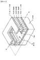
一例として、スピント型電界放出素子を適用した表示装置の概念図を図27にし、カソード・パネル50及びアノード・パネル60の一部分の模式的な分解斜視図を従来例として図63に示す。かかる表示装置を構成するスピント型電界放出素子は、支持体51に形成されたカソード電極52と、絶縁層53と、絶縁層53上に形成されたゲート電極54と、ゲート電極54及び絶縁層53を貫通して設けられた開口部55内に形成された円錐形の電子放出電極(エミッタ電極)56から構成されている。電子放出電極56が所定数、2次元マトリクス状に配列されて、1画素を構成する電子放出部が形成される。カソード電極52は、第1の方向に延びるストライプ状であり、ゲート電極54は、第1の方向とは異なる第2の方向に延びるストライプ状である(図63参照)。ストライプ状のカソード電極52とストライプ状のゲート電極54とが重複する領域が電子放出部10に相当する。カソード・パネル50は、かかる複数の電子放出部が形成されて構成されている。
【0006】
一方、アノード・パネル60は、基板61上に所定のパターンを有する蛍光体層62(具体的には、図63に示すように、赤色を発光する蛍光体層62R、緑色を発光する蛍光体層62G、及び、青色を発光する蛍光体層62B)が形成され、蛍光体層62がアノード電極63で覆われた構造を有する。尚、これらの蛍光体層62R,62G,62Bの間は、カーボン等の光吸収性材料から成るブラック・マトリクス64で埋め込まれており、表示画像の色濁りが防止されている。基板61上における蛍光体層62とアノード電極63の積層順を上記と逆にしても構わないが、この場合には、表示装置の観察面側から見てアノード電極63が蛍光体層62の手前に来るため、アノード電極63をITO(インジウム・錫酸化物)等の透明導電材料にて構成する必要がある。
【0007】
カソード電極52とゲート電極54との間に電圧を印加すると、その結果生じた電界によって電子放出電極56の先端から電子が放出される。そして、電子は、アノード・パネル60に設けられたアノード電極63に引き付けられ、アノード電極63と透明基板61との間に形成された発光体層である蛍光体層62に衝突する。その結果、蛍光体層62が励起されて発光し、所望の画像を得ることができる。電界放出素子の動作は、基本的に、ゲート電極54に印加される電圧によって制御される。
【0008】
図27及び図63に示した表示装置におけるスピント型電界放出素子の製造方法の概要を、以下、図31及び図32を参照しながら説明する。この製造方法は、基本的には、円錐形の電子放出電極56を金属材料の垂直蒸着により形成する方法である。即ち、開口部55に対して蒸着粒子は垂直に入射するが、開口端付近に形成されるオーバーハング状の堆積物による遮蔽効果を利用して、開口部55の底部に到達する蒸着粒子の量を漸減させ、円錐形の堆積物である電子放出電極56を自己整合的に形成する。ここでは、不要なオーバーハング状の堆積物の除去を容易とするために、絶縁層53及びゲート電極54上に剥離層57を予め形成しておく方法について、図31及び図32を参照して説明する。
【0009】
[工程−100]
先ず、例えばガラス基板から成る支持体51の上に、例えばポリシリコンから成るカソード電極用導電材料層をプラズマCVD法にて製膜した後、リソグラフィ技術及びドライエッチング技術に基づきカソード電極用導電材料層をパターニングして、ストライプ状のカソード電極52を形成する。その後、全面にSiO2から成る絶縁層53をCVD法にて、ゲート電極用導電材料層(例えば、TiN層)をスパッタ法にて、順次製膜し、次いで、ゲート電極用導電材料層をリソグラフィ技術及びドライエッチング技術にてパターニングすることによってゲート電極用導電材料層から成り、開口部55を有するストライプ状のゲート電極54を形成する。その後、絶縁層53に、例えば直径1μm程度の開口部55を形成する(図31の(A)参照)。
【0010】
[工程−110]
次に、図31の(B)に示すように、支持体51を回転させながらゲート電極54上を含む絶縁層53上にニッケル(Ni)を斜め蒸着することにより、剥離層57を形成する。このとき、支持体51の法線に対する蒸着粒子の入射角を十分に大きく選択することにより(例えば、入射角65度〜85度)、開口部55の底部にニッケルを殆ど堆積させることなく、絶縁層53及びゲート電極54の上に剥離層57を形成することができる。剥離層57は、開口部55の開口端から庇状に張り出しており、これによって開口部55が実質的に縮径される。
【0011】
[工程−120]
次に、全面に例えば導電材料としてモリブデン(Mo)を垂直蒸着する(入射角3度〜10度)。このとき、図32の(A)に示すように、剥離層57上でオーバーハング形状を有する導電材料層56Aが成長するに伴い、開口部55の実質的な直径が次第に縮小されるので、開口部55の底部において堆積に寄与する蒸着粒子は、次第に開口部55の中央付近を通過するものに限られるようになる。その結果、開口部55の底部には円錐形の堆積物が形成され、この円錐形の堆積物が電子放出電極56となる。
【0012】
[工程−130]
その後、図32の(B)に示すように、リフト・オフ法にて剥離層57を絶縁層53及びゲート電極54の表面から剥離し、絶縁層53及びゲート電極54の上方の導電材料層56Aを選択的に除去する。こうして、複数のスピント型電界放出素子が形成されたカソード・パネルを得ることができる。
【0013】
電界放出素子においては、ゲート電極54に印加される電圧とカソード電極52に印加される電圧の電位差ΔVが或る閾値電位ΔVth以上になると、電子放出電極56の先端部から電子が放出され始める。そして、例えばゲート電極54に印加される電圧の増加(即ち、電位差ΔVの増加)に伴い、電子放出電極56の先端部からの電子の放出によって生成する放出電子電流が急激に増加する。
【0014】
【発明が解決しようとする課題】
ところで、大型の表示装置を製造するためには、極めて清浄な処理と加工精度が要求される。例えば、38万画素のカラー表示装置を製造するためには114万の冷陰極電界電子放出部を形成する必要がある。また、スピント型電界放出素子から表示装置を構成する場合には、1つの冷陰極電界電子放出部を数十乃至千個程度のスピント型電界放出素子から構成しなければならない。従って、数μm未満にそれぞれが近接した数千万以上の微細な電界放出素子を作製する必要がある。また、電子放出電極56の先端部とゲート電極54の開口端面との間の距離は、0.12μm〜1.2μm程度とすることが、低い駆動電圧で大きな放出電子電流を得るために好適である。
【0015】
然るに、上述のスピント型電界放出素子の製造工程においては、大面積の表示装置を製造するために大面積の支持体(例えば、ガラス基板)全体に亙って剥離層57の剥離を行う必要があるが、かかる剥離層57の剥離は電界放出素子の欠陥発生の原因となる。また、ドライプロセスにおいても、大面積の支持体の加工に際して反応生成物の蓄積量が増加し、パーティクルにより電界放出素子に欠陥が発生し易くなる。ゲート電極54と電子放出電極56との間に導電性の異物が存在すると、ゲート電極54と電子放出電極56とが短絡する結果、電界放出素子から電子が放出されなくなり、表示装置においては暗点が出現する。カソード・パネルにおいては、通常、複数の冷陰極電界電子放出部が1次元的(ストライプ状)に配列された冷陰極電界電子放出領域列が複数並置されているので、電界放出素子の短絡が発生すると、かかる電界放出素子を含むストライプ状の冷陰極電界電子放出部列の一列全体の完全なる表示が出来なくなる場合もある。
【0016】
このような電界放出素子の短絡に起因した問題の発生を回避するための方法として、図64の(A)の模式的な一部端面図に示すように、電子放出電極56とカソード電極52との間に、例えば2MΩ程度の抵抗体層を形成する方法が挙げられる。然るに、電界放出素子が短絡状態にあると、ゲート電極54とカソード電極52との間を電子放出電極56及び抵抗体層を介して漏れ電流が流れる結果となり、消費電流の増加に繋がる。ゲート電極54に印加される電圧とカソード電極52に印加される電圧との差をΔV、抵抗体層の電気抵抗値をRとした場合、電界放出素子の短絡によって消費される消費電力Pは以下のとおりとなる。尚、nは短絡状態にある電界放出素子の個数である。
【0017】
P=n(ΔV2/R)
【0018】
消費電力Pを小さくするためには、抵抗体層の電気抵抗値Rを大きくすればよいが、電気抵抗値Rを大きくすると、図64の(B)に等価回路を示すように、ゲート電極54とカソード電極52との間の層間容量成分Cに電気抵抗値Rを付加した状態となり、時定数が大きくなる。それ故、ゲート電極54及びカソード電極52に印加される駆動信号に遅延が生じる結果、表示装置の動作速度が遅くなる。従って、抵抗体層の電気抵抗値Rは余り大きくすることはできないし、可能ならば、抵抗体層を設けないことが望ましい。
【0019】
また、電界放出素子に関する問題として、電界放出素子の電子放出特性のバラツキが挙げられる。電界放出素子は、カソード・パネル上に数十万個から数億個もの単位で同一プロセスにより形成されるが、個々の電界放出素子は電子顕微鏡下で一見同じように観察されても、電界放出素子の閾値電位ΔVthにはバラツキが存在する。そして、閾値電位ΔVthが異常に低い値を示す電界放出素子が存在する場合、正常な閾値電位ΔVthを示す電界放出素子が動作をしない電位差の状態にあっても、閾値電位ΔVthが異常に低い値を示す電界放出素子は動作状態となる。その結果、表示装置においては輝点が出現するといった問題が生じる。
【0020】
従って、本発明の目的は、たとえ冷陰極電界電子放出部に欠陥が発生したとしても、動作上、かかる冷陰極電界電子放出部を排除することができ、あるいは又、冷陰極電界電子放出部の欠陥部分を動作させなくすることができ、冷陰極電界電子放出表示装置の製造歩留まりの低下を招くことのない、冷陰極電界電子放出表示装置用カソード・パネル、及び、かかる冷陰極電界電子放出表示装置用カソード・パネルが組み込まれた冷陰極電界電子放出表示装置、並びに、冷陰極電界電子放出表示装置用カソード・パネルの製造方法を提供することにある。
【0021】
【課題を解決するための手段】
上記の目的を達成するための本発明の第1の態様に係る冷陰極電界電子放出表示装置用カソード・パネルは、
(イ)複数の幹配線、
(ロ)各幹配線から延びる複数の枝配線、並びに、
(ハ)各枝配線に接続された冷陰極電界電子放出部、
を具備する冷陰極電界電子放出表示装置用カソード・パネルであって、
動作不良の冷陰極電界電子放出部と幹配線とを接続する枝配線は切断されていることを特徴とする。
【0022】
上記の目的を達成するための本発明の第2の態様に係る冷陰極電界電子放出表示装置用カソード・パネルは、
(イ)複数の幹配線、
(ロ)各幹配線から延びる複数の枝配線、並びに、
(ハ)各枝配線に接続された冷陰極電界電子放出部、
を具備する冷陰極電界電子放出表示装置用カソード・パネルであって、
短絡状態にある冷陰極電界電子放出部と幹配線とを接続する枝配線は断線していることを特徴とする。
【0023】
本発明の第2の態様に係る冷陰極電界電子放出表示装置用カソード・パネルにおいては、各冷陰極電界電子放出部は、複数の冷陰極電界電子放出部ユニットから構成されており、各冷陰極電界電子放出部ユニットは枝配線を介して幹配線に接続されている構成とすることが、例えば1つの冷陰極電界電子放出部ユニットに短絡が生じた場合であっても、外見上、遜色のない画素を得るために好ましい。
【0024】
上記の目的を達成するための本発明の第3の態様に係る冷陰極電界電子放出表示装置用カソード・パネルは、
(イ)複数の幹配線、
(ロ)各幹配線から延びる、複数の第1枝配線及び複数の第2枝配線、並びに、
(ハ)複数の冷陰極電界電子放出領域、
を具備する冷陰極電界電子放出表示装置用カソード・パネルであって、
各冷陰極電界電子放出領域は、幹配線から延びる第1枝配線に接続された第1冷陰極電界電子放出部、及び、該幹配線から延びる第2枝配線に接続された第2冷陰極電界電子放出部から構成されており、
冷陰極電界電子放出領域を構成する一方の冷陰極電界電子放出部が動作不良である場合、該一方の冷陰極電界電子放出部と幹配線とを接続する枝配線は切断されており、
冷陰極電界電子放出領域を構成する両方の冷陰極電界電子放出部の動作が正常な場合、該冷陰極電界電子放出領域を構成するいずれか一方の冷陰極電界電子放出部と幹配線とを接続する枝配線は切断されていることを特徴とする。
【0025】
上記の目的を達成するための本発明の第4の態様に係る冷陰極電界電子放出表示装置用カソード・パネルは、
(イ)複数の幹配線、
(ロ)各幹配線から延びる、複数の第1枝配線及び複数の第2枝配線、並びに、
(ハ)複数の冷陰極電界電子放出領域、
を具備する冷陰極電界電子放出表示装置用カソード・パネルであって、
各冷陰極電界電子放出領域は、幹配線から延びる第1枝配線に接続された第1冷陰極電界電子放出部、及び、該幹配線から延びる第2枝配線に接続された第2冷陰極電界電子放出部から構成されており、
冷陰極電界電子放出領域を構成する冷陰極電界電子放出部が短絡状態にある場合、該冷陰極電界電子放出部と幹配線とを接続する枝配線は断線しており、
冷陰極電界電子放出領域を構成する両方の冷陰極電界電子放出部の動作が正常な場合、該冷陰極電界電子放出領域を構成するいずれか一方の冷陰極電界電子放出部と幹配線とを接続する枝配線は切断されていることを特徴とする。
【0026】
上記の目的を達成するための本発明の第5の態様に係る冷陰極電界電子放出表示装置用カソード・パネルは、
(イ)複数の幹配線、
(ロ)各幹配線から延びる複数の枝配線、並びに、
(ハ)複数の冷陰極電界電子放出領域、
を具備する冷陰極電界電子放出表示装置用カソード・パネルであって、
各冷陰極電界電子放出領域は、幹配線から延びる枝配線に接続された第1冷陰極電界電子放出部、及び、第2冷陰極電界電子放出部から構成されており、
第1冷陰極電界電子放出部が動作不良の場合、該第1冷陰極電界電子放出部と幹配線とを接続する枝配線は切断されており、且つ、該第1冷陰極電界電子放出部が含まれる冷陰極電界電子放出領域を構成する第2冷陰極電界電子放出部は該幹配線に電気的に接続されていることを特徴とする。
【0027】
上記の目的を達成するための本発明の第6の態様に係る冷陰極電界電子放出表示装置用カソード・パネルは、
(イ)複数の幹配線、
(ロ)各幹配線から延びる複数の枝配線、並びに、
(ハ)複数の冷陰極電界電子放出領域、
を具備する冷陰極電界電子放出表示装置用カソード・パネルであって、
各冷陰極電界電子放出領域は、幹配線から延びる枝配線に接続された第1冷陰極電界電子放出部、及び、第2冷陰極電界電子放出部から構成されており、
第1冷陰極電界電子放出部が短絡状態にある場合、該第1冷陰極電界電子放出部と幹配線とを接続する枝配線は断線しており、且つ、該第1冷陰極電界電子放出部が含まれる冷陰極電界電子放出領域を構成する第2冷陰極電界電子放出部は該幹配線に電気的に接続されていることを特徴とする。
【0028】
上記の目的を達成するための本発明の第7の態様に係る冷陰極電界電子放出表示装置用カソード・パネルは、
(イ)それぞれが第1の幹配線と第2の幹配線から構成された、複数の幹配線、
(ロ)各第1の幹配線から延びる複数の第1枝配線、
(ハ)各第2の幹配線から延びる複数の第2枝配線、並びに、
(ニ)各第1及び第2枝配線に接続された冷陰極電界電子放出部、
を具備する冷陰極電界電子放出表示装置用カソード・パネルであって、
動作不良の冷陰極電界電子放出部に対しては、冷陰極電界電子放出部が動作しないように枝配線が切断されていることを特徴とする。
【0029】
上記の目的を達成するための本発明の第8の態様に係る冷陰極電界電子放出表示装置用カソード・パネルは、
(イ)2次元マトリックス状に形成された複数の冷陰極電界電子放出部から構成された有効領域、及び、
(ロ)該有効領域の周辺部に配置され、2次元マトリックス状に形成された複数の冷陰極電界電子放出部から構成された無効領域、
から成り、
有効領域を構成する冷陰極電界電子放出部は、冷陰極電界電子放出部を駆動するための電源に接続され、
無効領域を構成する冷陰極電界電子放出部は該電源に接続されていないことを特徴とする。
【0030】
上記の目的を達成するための本発明の第9の態様に係る冷陰極電界電子放出表示装置用カソード・パネルは、
冷陰極電界電子放出部群が複数並置されて成る冷陰極電界電子放出表示装置用カソード・パネルであって、
該冷陰極電界電子放出部群は、複数の冷陰極電界電子放出部が1次元的に配列されて成る冷陰極電界電子放出部列がN列(但し、Nは2以上の自然数)、並置されて成り、
各冷陰極電界電子放出部群において、(N−1)列以下の一定数の冷陰極電界電子放出部列が選択され、かかる選択された冷陰極電界電子放出部列は冷陰極電界電子放出部を駆動するための電源に接続され、選択されない冷陰極電界電子放出部列は該電源に接続されていないことを特徴とする。
【0031】
上記の目的を達成するための本発明の第1の態様に係る冷陰極電界電子放出表示装置用カソード・パネルの製造方法は、本発明の第1の態様に係る冷陰極電界電子放出表示装置用カソード・パネルを製造するための方法である。即ち、
(イ)複数の幹配線、
(ロ)各幹配線から延びる複数の枝配線、並びに、
(ハ)各枝配線に接続された冷陰極電界電子放出部、
を具備する冷陰極電界電子放出表示装置用カソード・パネルの製造方法であって、
冷陰極電界電子放出部の動作試験を行い、
動作不良が検出された冷陰極電界電子放出部と幹配線とを接続する枝配線を切断することを特徴とする。
【0032】
上記の目的を達成するための本発明の第2の態様に係る冷陰極電界電子放出表示装置用カソード・パネルの製造方法は、本発明の第2の態様に係る冷陰極電界電子放出表示装置用カソード・パネルを製造するための方法である。即ち、
(イ)複数の幹配線、
(ロ)各幹配線から延びる複数の枝配線、並びに、
(ハ)各枝配線に接続された冷陰極電界電子放出部、
を具備する冷陰極電界電子放出表示装置用カソード・パネルの製造方法であって、
幹配線から枝配線を介して冷陰極電界電子放出部に電圧を印加する冷陰極電界電子放出部の短絡試験を行い、
短絡が生じている冷陰極電界電子放出部と幹配線とを接続する枝配線を、枝配線を流れる電流によって断線させることを特徴とする。
【0033】
本発明の第2の態様に係る冷陰極電界電子放出表示装置用カソード・パネルの製造方法においては、各冷陰極電界電子放出部は、複数の冷陰極電界電子放出部ユニットから構成されており、各冷陰極電界電子放出部ユニットは枝配線を介して幹配線に接続されている構成とすることが、例えば1つの冷陰極電界電子放出部ユニットに短絡が生じた場合であっても、外見上、遜色のない画素を得るために好ましい。
【0034】
上記の目的を達成するための本発明の第3の態様に係る冷陰極電界電子放出表示装置用カソード・パネルの製造方法は、本発明の第3の態様に係る冷陰極電界電子放出表示装置用カソード・パネルを製造するための方法である。即ち、
(イ)複数の幹配線、
(ロ)各幹配線から延びる、複数の第1枝配線及び複数の第2枝配線、並びに、
(ハ)複数の冷陰極電界電子放出領域、
を具備し、
各冷陰極電界電子放出領域は、幹配線から延びる第1枝配線に接続された第1冷陰極電界電子放出部、及び、該幹配線から延びる第2枝配線に接続された第2冷陰極電界電子放出部から構成された、冷陰極電界電子放出表示装置用カソード・パネルの製造方法であって、
冷陰極電界電子放出領域の動作試験を行い、
動作不良が検出された冷陰極電界電子放出領域においては、該冷陰極電界電子放出領域を構成するいずれか一方の冷陰極電界電子放出部と幹配線とを接続する枝配線を切断し、
動作が正常の冷陰極電界電子放出領域においては、該冷陰極電界電子放出領域を構成するいずれか一方の冷陰極電界電子放出部と幹配線とを接続する枝配線を切断することを特徴とする。
【0035】
上記の目的を達成するための本発明の第4の態様に係る冷陰極電界電子放出表示装置用カソード・パネルの製造方法は、本発明の第4の態様に係る冷陰極電界電子放出表示装置用カソード・パネルを製造するための方法である。即ち、
(イ)複数の幹配線、
(ロ)各幹配線から延びる、複数の第1枝配線及び複数の第2枝配線、並びに、
(ハ)複数の冷陰極電界電子放出領域、
を具備し、
各冷陰極電界電子放出領域は、幹配線から延びる第1枝配線に接続された第1冷陰極電界電子放出部、及び、該幹配線から延びる第2枝配線に接続された第2冷陰極電界電子放出部から構成された、冷陰極電界電子放出表示装置用カソード・パネルの製造方法であって、
幹配線から枝配線を介して冷陰極電界電子放出部に電圧を印加する冷陰極電界電子放出部の短絡試験を行い、
短絡状態にある冷陰極電界電子放出領域においては、短絡状態にある冷陰極電界電子放出部と幹配線とを接続する枝配線を、枝配線を流れる電流によって断線させ、
動作が正常の冷陰極電界電子放出領域においては、該冷陰極電界電子放出領域を構成するいずれか一方の冷陰極電界電子放出部と幹配線とを接続する枝配線を切断することを特徴とする。
【0036】
上記の目的を達成するための本発明の第5の態様に係る冷陰極電界電子放出表示装置用カソード・パネルの製造方法は、本発明の第5の態様に係る冷陰極電界電子放出表示装置用カソード・パネルを製造するための方法である。即ち、
(イ)複数の幹配線、
(ロ)各幹配線から延びる複数の枝配線、並びに、
(ハ)複数の冷陰極電界電子放出領域、
を具備し、
各冷陰極電界電子放出領域は、幹配線から延びる枝配線に接続された第1冷陰極電界電子放出部、及び、第2冷陰極電界電子放出部から構成された、冷陰極電界電子放出表示装置用カソード・パネルの製造方法であって、
第1冷陰極電界電子放出部の動作試験を行い、
動作不良が検出された第1冷陰極電界電子放出部と幹配線とを接続する枝配線を切断し、且つ、該第1冷陰極電界電子放出部が含まれる冷陰極電界電子放出領域を構成する第2冷陰極電界電子放出部を該幹配線に電気的に接続することを特徴とする。
【0037】
上記の目的を達成するための本発明の第6の態様に係る冷陰極電界電子放出表示装置用カソード・パネルの製造方法は、本発明の第6の態様に係る冷陰極電界電子放出表示装置用カソード・パネルを製造するための方法である。即ち、
(イ)複数の幹配線、
(ロ)各幹配線から延びる複数の枝配線、並びに、
(ハ)複数の冷陰極電界電子放出領域、
を具備し、
各冷陰極電界電子放出領域は、幹配線から延びる枝配線に接続された第1冷陰極電界電子放出部、及び、第2冷陰極電界電子放出部から構成された、冷陰極電界電子放出表示装置用カソード・パネルの製造方法であって、
幹配線から枝配線を介して第1冷陰極電界電子放出部に電圧を印加する冷陰極電界電子放出部の短絡試験を行い、
短絡状態にある冷陰極電界電子放出領域においては、該第1冷陰極電界電子放出部と幹配線とを接続する枝配線を、枝配線を流れる電流によって断線させ、且つ、該第1冷陰極電界電子放出部が含まれる冷陰極電界電子放出領域を構成する第2冷陰極電界電子放出部を該幹配線に電気的に接続することを特徴とする。
【0038】
上記の目的を達成するための本発明の第7の態様に係る冷陰極電界電子放出表示装置用カソード・パネルの製造方法は、本発明の第7の態様に係る冷陰極電界電子放出表示装置用カソード・パネルを製造するための方法である。即ち、
(イ)それぞれが第1の幹配線と第2の幹配線から構成された、複数の幹配線、
(ロ)各第1の幹配線から延びる複数の第1枝配線、
(ハ)各第2の幹配線から延びる複数の第2枝配線、並びに、
(ニ)各第1及び第2枝配線に接続された冷陰極電界電子放出部、
を具備する冷陰極電界電子放出表示装置用カソード・パネルの製造方法であって、
冷陰極電界電子放出部の動作試験を行い、
動作不良が検出された冷陰極電界電子放出部においては、冷陰極電界電子放出部が動作しないように枝配線を切断することを特徴とする。
【0039】
上記の目的を達成するための本発明の第8の態様に係る冷陰極電界電子放出表示装置用カソード・パネルの製造方法は、本発明の第9の態様に係る冷陰極電界電子放出表示装置用カソード・パネルを製造するための方法である。即ち、
冷陰極電界電子放出部群が複数並置されて成る冷陰極電界電子放出表示装置用カソード・パネルの製造方法であって、
該冷陰極電界電子放出部群は、複数の冷陰極電界電子放出部が1次元的に配列されて成る冷陰極電界電子放出部列がN列(但し、Nは2以上の自然数)、並置されて成り、
冷陰極電界電子放出部の動作試験を行い、
各冷陰極電界電子放出部群において、動作不良が検出された冷陰極電界電子放出部を含む冷陰極電界電子放出部列を除く(N−1)列以下の一定数の冷陰極電界電子放出部列を選択し、かかる選択された冷陰極電界電子放出部列を、冷陰極電界電子放出部を駆動するための電源に接続し、
各冷陰極電界電子放出部群において、冷陰極電界電子放出部の動作が正常である場合には、(N−1)列以下の一定数の冷陰極電界電子放出部列を選択し、かかる選択された冷陰極電界電子放出部列を該電源に接続することを特徴とする。
【0040】
上記の目的を達成するための本発明の第1の態様に係る冷陰極電界電子放出表示装置には、本発明の第1の態様に係る冷陰極電界電子放出表示装置用カソード・パネルが備えられている。即ち、本発明の第1の態様に係る冷陰極電界電子放出表示装置は、
複数の画素から構成され、
各画素は、カソード・パネル上に設けられた冷陰極電界電子放出部と、冷陰極電界電子放出部に対向してアノード・パネル上に設けられたアノード電極及び蛍光体層とから構成された冷陰極電界電子放出表示装置であって、
該カソード・パネルは、
(イ)複数の幹配線、
(ロ)各幹配線から延びる複数の枝配線、並びに、
(ハ)各枝配線に接続された冷陰極電界電子放出部、
を具備し、
動作不良の冷陰極電界電子放出部と幹配線とを接続する枝配線は切断されていることを特徴とする。
【0041】
上記の目的を達成するための本発明の第2の態様に係る冷陰極電界電子放出表示装置には、本発明の第2の態様に係る冷陰極電界電子放出表示装置用カソード・パネルが備えられている。即ち、本発明の第2の態様に係る冷陰極電界電子放出表示装置は、
複数の画素から構成され、
各画素は、カソード・パネル上に設けられた冷陰極電界電子放出部と、冷陰極電界電子放出部に対向してアノード・パネル上に設けられたアノード電極及び蛍光体層とから構成された冷陰極電界電子放出表示装置であって、
該カソード・パネルは、
(イ)複数の幹配線、
(ロ)各幹配線から延びる複数の枝配線、並びに、
(ハ)各枝配線に接続された冷陰極電界電子放出部、
を具備し、
短絡状態にある冷陰極電界電子放出部と幹配線とを接続する枝配線は断線していることを特徴とする。
【0042】
本発明の第2の態様に係る冷陰極電界電子放出表示装置においては、各冷陰極電界電子放出部は、複数の冷陰極電界電子放出部ユニットから構成されており、各冷陰極電界電子放出部ユニットは枝配線を介して幹配線に接続されている構成とすることが、例えば1つの冷陰極電界電子放出部ユニットに短絡が生じた場合であっても、外見上、遜色のない画素を得るために好ましい。
【0043】
上記の目的を達成するための本発明の第3の態様に係る冷陰極電界電子放出表示装置には、本発明の第3の態様に係る冷陰極電界電子放出表示装置用カソード・パネルが備えられている。即ち、本発明の第3の態様に係る冷陰極電界電子放出表示装置は、
複数の画素から構成され、
各画素は、カソード・パネル上に設けられた冷陰極電界電子放出領域と、冷陰極電界電子放出領域に対向してアノード・パネル上に設けられたアノード電極及び蛍光体層とから構成された冷陰極電界電子放出表示装置であって、
該カソード・パネルは、
(イ)複数の幹配線、
(ロ)各幹配線から延びる、複数の第1枝配線及び複数の第2枝配線、並びに、
(ハ)複数の冷陰極電界電子放出領域、
を具備し、
各冷陰極電界電子放出領域は、幹配線から延びる第1枝配線に接続された第1冷陰極電界電子放出部、及び、該幹配線から延びる第2枝配線に接続された第2冷陰極電界電子放出部から構成されており、
冷陰極電界電子放出領域を構成する一方の冷陰極電界電子放出部が動作不良である場合、該一方の冷陰極電界電子放出部と幹配線とを接続する枝配線は切断されており、
冷陰極電界電子放出領域を構成する両方の冷陰極電界電子放出部の動作が正常な場合、該冷陰極電界電子放出領域を構成するいずれか一方の冷陰極電界電子放出部と幹配線とを接続する枝配線は切断されていることを特徴とする。
【0044】
上記の目的を達成するための本発明の第4の態様に係る冷陰極電界電子放出表示装置には、本発明の第4の態様に係る冷陰極電界電子放出表示装置用カソード・パネルが備えられている。即ち、本発明の第4の態様に係る冷陰極電界電子放出表示装置は、
複数の画素から構成され、
各画素は、カソード・パネル上に設けられた冷陰極電界電子放出領域と、冷陰極電界電子放出領域に対向してアノード・パネル上に設けられたアノード電極及び蛍光体層とから構成された冷陰極電界電子放出表示装置であって、
該カソード・パネルは、
(イ)複数の幹配線、
(ロ)各幹配線から延びる、複数の第1枝配線及び複数の第2枝配線、並びに、
(ハ)複数の冷陰極電界電子放出領域、
を具備し、
各冷陰極電界電子放出領域は、幹配線から延びる第1枝配線に接続された第1冷陰極電界電子放出部、及び、該幹配線から延びる第2枝配線に接続された第2冷陰極電界電子放出部から構成されており、
冷陰極電界電子放出領域を構成する冷陰極電界電子放出部が短絡状態にある場合、該冷陰極電界電子放出部と幹配線とを接続する枝配線は断線しており、
冷陰極電界電子放出領域を構成する両方の冷陰極電界電子放出部の動作が正常な場合、該冷陰極電界電子放出領域を構成するいずれか一方の冷陰極電界電子放出部と幹配線とを接続する枝配線は切断されていることを特徴とする。
【0045】
上記の目的を達成するための本発明の第5の態様に係る冷陰極電界電子放出表示装置には、本発明の第5の態様に係る冷陰極電界電子放出表示装置用カソード・パネルが備えられている。即ち、本発明の第5の態様に係る冷陰極電界電子放出表示装置は、
複数の画素から構成され、
各画素は、カソード・パネル上に設けられた冷陰極電界電子放出領域と、冷陰極電界電子放出領域に対向してアノード・パネル上に設けられたアノード電極及び蛍光体層とから構成された冷陰極電界電子放出表示装置であって、
該カソード・パネルは、
(イ)複数の幹配線、
(ロ)各幹配線から延びる複数の枝配線、並びに、
(ハ)複数の冷陰極電界電子放出領域、
を具備し、
各冷陰極電界電子放出領域は、幹配線から延びる枝配線に接続された第1冷陰極電界電子放出部、及び、第2冷陰極電界電子放出部から構成されており、
第1冷陰極電界電子放出部が動作不良の場合、該第1冷陰極電界電子放出部と幹配線とを接続する枝配線は切断されており、且つ、該第1冷陰極電界電子放出部が含まれる冷陰極電界電子放出領域を構成する第2冷陰極電界電子放出部は該幹配線に電気的に接続されていることを特徴とする。
【0046】
上記の目的を達成するための本発明の第6の態様に係る冷陰極電界電子放出表示装置には、本発明の第6の態様に係る冷陰極電界電子放出表示装置用カソード・パネルが備えられている。即ち、本発明の第6の態様に係る冷陰極電界電子放出表示装置は、
複数の画素から構成され、
各画素は、カソード・パネル上に設けられた冷陰極電界電子放出領域と、冷陰極電界電子放出領域に対向してアノード・パネル上に設けられたアノード電極及び蛍光体層とから構成された冷陰極電界電子放出表示装置であって、
該カソード・パネルは、
(イ)複数の幹配線、
(ロ)各幹配線から延びる複数の枝配線、並びに、
(ハ)複数の冷陰極電界電子放出領域、
を具備し、
各冷陰極電界電子放出領域は、幹配線から延びる枝配線に接続された第1冷陰極電界電子放出部、及び、第2冷陰極電界電子放出部から構成されており、
第1冷陰極電界電子放出部が短絡状態にある場合、該第1冷陰極電界電子放出部と幹配線とを接続する枝配線は断線しており、且つ、該第1冷陰極電界電子放出部が含まれる冷陰極電界電子放出領域を構成する第2冷陰極電界電子放出部は該幹配線に電気的に接続されていることを特徴とする。
【0047】
上記の目的を達成するための本発明の第7の態様に係る冷陰極電界電子放出表示装置には、本発明の第7の態様に係る冷陰極電界電子放出表示装置用カソード・パネルが備えられている。即ち、本発明の第7の態様に係る冷陰極電界電子放出表示装置は、
複数の画素から構成され、
各画素は、カソード・パネル上に設けられた冷陰極電界電子放出部と、冷陰極電界電子放出部に対向してアノード・パネル上に設けられたアノード電極及び蛍光体層とから構成された冷陰極電界電子放出表示装置であって、
該カソード・パネルは、
(イ)それぞれが第1の幹配線と第2の幹配線から構成された、複数の幹配線、
(ロ)各第1の幹配線から延びる複数の第1枝配線、
(ハ)各第2の幹配線から延びる複数の第2枝配線、並びに、
(ニ)各第1及び第2枝配線に接続された冷陰極電界電子放出部、
を具備し、
動作不良の冷陰極電界電子放出部に対しては、冷陰極電界電子放出部が動作しないように枝配線が切断されていることを特徴とする。
【0048】
上記の目的を達成するための本発明の第8の態様に係る冷陰極電界電子放出表示装置には、本発明の第8の態様に係る冷陰極電界電子放出表示装置用カソード・パネルが備えられている。即ち、本発明の第8の態様に係る冷陰極電界電子放出表示装置は、
複数の画素から構成され、
各画素は、カソード・パネル上に設けられた冷陰極電界電子放出部と、冷陰極電界電子放出部に対向してアノード・パネル上に設けられたアノード電極及び蛍光体層とから構成された冷陰極電界電子放出表示装置であって、
該カソード・パネルは、
(イ)2次元マトリックス状に形成された複数の冷陰極電界電子放出部から構成された有効領域、及び、
(ロ)該有効領域の周辺部に配置され、2次元マトリックス状に形成された複数の冷陰極電界電子放出部から構成された無効領域、
を具備し、
有効領域を構成する冷陰極電界電子放出部は、冷陰極電界電子放出部を駆動するための電源に接続され、
無効領域を構成する冷陰極電界電子放出部は該電源に接続されていないことを特徴とする。
【0049】
上記の目的を達成するための本発明の第9の態様に係る冷陰極電界電子放出表示装置には、本発明の第9の態様に係る冷陰極電界電子放出表示装置用カソード・パネルが備えられている。即ち、本発明の第9の態様に係る冷陰極電界電子放出表示装置は、
複数の画素から構成され、
各画素は、カソード・パネル上に設けられた冷陰極電界電子放出部と、冷陰極電界電子放出部に対向してアノード・パネル上に設けられたアノード電極及び蛍光体層とから構成された冷陰極電界電子放出表示装置であって、
該カソード・パネルには、冷陰極電界電子放出部群が複数並置されており、
該冷陰極電界電子放出部群は、複数の冷陰極電界電子放出部が1次元的に配列されて成る冷陰極電界電子放出部列がN列(但し、Nは2以上の自然数)、並置されて成り、
各冷陰極電界電子放出部群において、(N−1)列以下の一定数の冷陰極電界電子放出部列が選択され、かかる選択された冷陰極電界電子放出部列は冷陰極電界電子放出部を駆動するための電源に接続され、選択されない冷陰極電界電子放出部列は該電源に接続されていないことを特徴とする。
【0050】
尚、「枝配線を切断する」とは、外部からの物理的あるいは化学的な作用に基づき枝配線の一部分を除去することを意味し、「枝配線が切断されている」とは、外部からの物理的あるいは化学的作用に基づき枝配線の一部分が除去されている状態を意味する。また、「枝配線を断線させる」とは、枝配線の一部分を溶融することによって除去することを意味し、あるいは又、枝配線に過剰の電流を流すことによって生じた電流ストレスによるエレクトロマイグレーションに基づき枝配線を切り、枝配線を不導通状態とすることを意味し、「枝配線が断線する」とは、枝配線の一部分が溶融することによって除去されている状態、あるいは又、枝配線に過剰の電流を流すことによって生じた電流ストレスによるエレクトロマイグレーションに基づき枝配線が切れ、枝配線が不導通状態となっていることを意味する。「動作不良の冷陰極電界電子放出部」とは、表示装置において暗点あるいは輝点を出現させるような冷陰極電界電子放出部を意味する。冷陰極電界電子放出素子の短絡は、導電性異物の存在によって生じる場合もあるし、冷陰極電界電子放出素子の製造時、冷陰極電界電子放出素子を構成する導電性材料が残存することによって生じる場合もある。
【0051】
本発明の第2、第4、第6の態様に係る冷陰極電界電子放出表示装置用カソード・パネルにおいては、また、本発明の第2、第4、第6の態様に係る冷陰極電界電子放出表示装置用カソード・パネルの製造方法においては、更には、本発明の第2、第4、第6の態様に係る冷陰極電界電子放出表示装置においては、枝配線は、アルミニウム層あるいはアルミニウム合金層から成り、あるいは又、アルミニウム層あるいはアルミニウム合金層から成る第1の枝配線部分と、アルミニウム層あるいはアルミニウム合金層とバリアメタル層の2層構造を有する第2の枝配線部分とから構成されていることが、枝配線を流れる電流によって枝配線を確実に断線させるといった観点から好ましい。アルミニウム層は純度99%以上のアルミニウムから構成することが好ましい。また、アルミニウム合金層として、Al−Si、Al−Cu、Al−Si−Cuを例示することができる。尚、SiやCuは、総量として1〜2原子%、Al中に含有されていることが好ましい。バリアメタル層を構成する材料は、アルミニウムあるいはアルミニウム合金の融点よりも高い融点を有する材料である必要があり、タングステン(W)、モリブデン(Mo)、チタン(Ti)といった高融点金属材料、TiN等の窒化物、Ti−W等の合金、例えば高融点金属材料の合金や化合物を例示することができる。尚、枝配線の断線を容易に生じさせるために、枝配線の少なくとも一部分の幅を0.5μm〜5μmとし、枝配線の長さを10μm以上、例えば0.5mm以下とすることが好ましいが、これらの値に限定するものではない。
【0052】
本発明の冷陰極電界電子放出表示装置用カソード・パネル及び冷陰極電界電子放出表示装置、並びに、冷陰極電界電子放出表示装置用カソード・パネルの製造方法(以下、これらを総称して、単に、本発明と呼ぶ場合がある)において、冷陰極電界電子放出部(以下、電子放出部と呼ぶ)は、複数(例えば、数十乃至千個程度)のスピント型電界放出素子、あるいは、複数(例えば、数十乃至数百個程度)のエッジ型電界放出素子、あるいは、1つ若しくは複数の平面型電界放出素子から構成することができる。
【0053】
本発明においては、動作不良の、あるいは短絡した電子放出部は幹配線から電気的に分離されているので、あるいは又、無効領域を構成する電子放出部や非選択の冷陰極電界電子放出部列は電子放出部を駆動するための電源に接続されていないので、かかる電子放出部、無効領域、あるいは非選択の冷陰極電界電子放出部列は電子放出に何ら寄与しない。従って、たとえ電子放出部に欠陥が発生したとしても、あるいは又、冷陰極電界電子放出領域に欠陥が存在していたとしても、動作上、かかる欠陥は排除される結果、表示装置の製造歩留まりの低下を招くことがない。
【0054】
【発明の実施の形態】
以下、図面を参照して、発明の実施の形態(以下、実施の形態と略称する)に基づき本発明を説明するが、それに先立ち、スピント型電界放出素子、エッジ型電界放出素子、及び、平面型電界放出素子の概要、並びに、これらの電界放出素子の基本的な製造工程を説明する。
【0055】
スピント型電界放出素子の構造は、図32の(B)に示したとおりである。即ち、スピント型電界放出素子は、
(イ)支持体51上に形成されたカソード電極52、
(ロ)カソード電極52上を含む支持体51上に形成された絶縁層53、
(ハ)絶縁層53上に形成されたゲート電極54、
(ニ)ゲート電極54及び絶縁層53を貫通した開口部55、並びに、
(ホ)開口部55の底部に位置するカソード電極52上に形成された錐状形状を有する電子放出電極56、
から構成されており、電子放出電極56の先端部から電子が放出される。スピント型電界放出素子の基本的な製造方法は、図31及び図32を参照して先に説明したとおりである。
【0056】
エッジ型電界放出素子の模式的な一部端面図を、図33の(A)に示す。このエッジ型電界放出素子は、
(イ)支持体71上に形成された第1絶縁層73、
(ロ)第1絶縁層73上に形成された電子放出層74、
(ハ)電子放出層74上を含む第1絶縁層73上に形成された第2絶縁層75、
(ニ)第2絶縁層75上に形成されたゲート電極76、並びに、
(ホ)少なくとも、ゲート電極76、第2絶縁層75及び電子放出層74を貫通した開口部78、
から成り、
開口部78の壁面から突出した電子放出層74の端部から電子が放出される。尚、このような構成のエッジ型電界放出素子を、便宜上、第1の構造のエッジ型電界放出素子と呼ぶ。
【0057】
エッジ型電界放出素子の変形例の模式的な一部端面図を、図33の(B)に示す。このエッジ型電界放出素子は、
(イ)支持体71上に形成された第1ゲート電極72、
(ロ)第1ゲート電極72上を含む支持体71上に形成された第1絶縁層73、
(ハ)第1絶縁層73上に形成された電子放出層74、
(ニ)電子放出層74上を含む第1絶縁層73上に形成された第2絶縁層75、
(ホ)第2絶縁層75上に形成された第2ゲート電極77、並びに、
(ヘ)第2ゲート電極77、第2絶縁層75、電子放出層74及び第1絶縁層73を貫通し、底部に第1ゲート電極72の表面が露出した開口部78、
から成り、
開口部78の壁面から突出した電子放出層74の端部74Aから電子が放出される。尚、開口部78近傍の支持体71等を一部切断して露出させた模式的な斜視図を図34に示す。ここで、図33の(B)に示した模式的な一部端面図は、図34の線A−Aに沿った端面図である。このような構成のエッジ型電界放出素子を、便宜上、第2の構造のエッジ型電界放出素子と呼ぶ。第2の構造のエッジ型電界放出素子においては、電子放出層74の下方に第1ゲート電極72が設けられているので、第1の構造のエッジ型電界放出素子と比較して、開口部78の壁面から突出した電子放出層74の端部74Aの近傍に一層高強度の電界を形成することができる。
【0058】
図33の(B)に示したエッジ型電界放出素子の製造方法を、以下、図35〜図37を参照して説明する。
【0059】
[工程−200]
先ず、例えばガラス基板から成る支持体71の上に、スパッタ法にて厚さ約0.2μmのタングステンから成る第1ゲート電極用導電材料層を成膜し、通常の手順に従ってリソグラフィ技術及びドライエッチング技術により第1ゲート電極用導電材料層をパターニングして、第1ゲート電極72を形成する(図35の(A)参照)。
【0060】
[工程−210]
次に、全面に第1絶縁層73を形成する。ここでは一例として、SiO2を約0.3μmの厚さに形成する。更に、この第1絶縁層73の上にタングステンから成る電子放出層用導電材料層を0.2μmの厚さに形成した後、所定の形状にパターニングし、電子放出層74を形成する(図35の(B)参照)。
【0061】
[工程−220]
次に、全面に例えばSiO2から成る第2絶縁層75を例えば約0.7μmの厚さに形成する。更に、この第2絶縁層75の上に厚さ約0.2μmのタングステンから成る第2ゲート電極用導電材料層を形成し、所定のパターニングを行うことによって、第2ゲート電極77を得ることができる(図35の(C)参照)。第2ゲート電極77の構成材料や厚さは、第1ゲート電極72と同じであってもよいし、異なっていてもよい。
【0062】
[工程−230]
その後、全面にレジスト層79を形成し、更に、このレジスト層79に、第2ゲート電極77の表面を一部露出させるようにレジスト開口部79Aを形成する。レジスト開口部79Aの平面形状は矩形であり、矩形の長辺はおおよそ100μm、短辺は数μm〜10μmである。続いて、レジスト開口部79Aの底面に露出した第2ゲート電極77を例えばRIE(反応性イオン・エッチング)法により異方的にエッチングし、開口部78Aを形成する(図36の(A)参照)。ここでは第2ゲート電極77をタングステンを用いて構成しているので、SF6ガスを用いたエッチングにより垂直壁を有する開口部78Aを形成することができる。
【0063】
[工程−240]
次に、図36の(B)に示すように、開口部78Aの底面に露出した第2絶縁層75を等方的にエッチングし、開口部78Bを形成する。ここでは第2絶縁層75をSiO2を用いて形成しているので、緩衝化フッ酸水溶液を用いたウェットエッチングを行う。開口部78Bの壁面は、開口部78Aの開口端面よりも後退するが、このときの後退量はエッチング時間の長短により制御することができる。ここでは、開口部78Bの下端が開口部78Aの開口端面よりも後退するまで、ウェットエッチングを行う。
【0064】
[工程−250]
次に、図37の(A)に示すように、開口部78Bの底面に露出した電子放出層74を、イオンを主エッチング種とする条件によりドライエッチングする。イオンを主エッチング種とするドライエッチングでは、被エッチング物へのバイアス電圧の印加やプラズマと磁界との相互作用を利用して荷電粒子であるイオンを加速することができるため、一般には異方性エッチングが進行し、被エッチング物の加工面は垂直壁となる。しかし、この[工程−250]では、プラズマ中の主エッチング種の中にも垂直以外の角度を有する入射成分が若干存在すること、及び開口部78Aの端部における散乱によってもこの斜め入射成分が生ずることにより、電子放出層74の露出面の中で、本来であれば開口部78Aによって遮蔽されてイオンが到達しないはずの領域にも、ある程度の確率で主エッチング種が入射する。このとき、電子放出層74の法線に対する入射角の小さい主エッチング種ほど入射確率は高く、入射角の大きい主エッチング種ほど入射確率は低い。従って、電子放出層74に形成された開口部78Cの上端部の位置は開口部78Bの下端部とほぼ揃っているものの、開口部78Cの下端部の位置はその上端部よりも突出した状態となる。つまり、電子放出層74の厚さが、突出方向の先端部に向けて薄くなり、端部が先鋭化される。ここでは、エッチング・ガスとしてSF6を用いることにより、電子放出層74の良好な加工を行うことができる。
【0065】
[工程−260]
次に、図37の(B)に示すように、開口部78Cの底面に露出した第1絶縁層73を等方的にエッチングし、開口部78Dを形成し、開口部78を完成させる。ここでは、上述の第2絶縁層75の場合と同様に、緩衝化フッ酸水溶液を用いたウェットエッチングを行う。開口部78Dの壁面は開口部78Cの下端部よりも後退する。このときの後退量はエッチング時間の長短により制御可能である。このとき、先に形成された開口部78Bの壁面は更に後退する。尚、開口部78の完成後にレジスト層79を除去すると、図33の(B)に示した構造を有するエッジ型電界放出素子が形成されたカソード・パネルを得ることができる。
【0066】
平面型電界放出素子の模式的な一部端面図を、図38に示す。この平面型電界放出素子は、
(イ)支持体81上に形成された電子放出層84、
(ロ)電子放出層84上を含む支持体81上に形成された絶縁層85、
(ハ)絶縁層85上に形成されたゲート電極86、並びに、
(ニ)ゲート電極86及び絶縁層85を貫通し、底部に電子放出層84の表面が露出した開口部88、
から成り、
開口部88の底部に露出した電子放出層84の表面から電子が放出される。
【0067】
図38に示した平面型電界放出素子の製造方法を、以下、図39を参照して説明する。
【0068】
[工程−300]
先ず、例えばガラス基板から成る支持体81の上に、スパッタ法により厚さ約0.2μmのタングステンから成る電子放出層用導電材料層を製膜し、通常の手順に従ってこの電子放出層用導電材料層をパターニングし、電子放出層84を形成する。次に、電子放出層84上を含む支持体81上に絶縁層85を形成する。ここでは一例としてTEOS(テトラエトキシシラン)を原料ガスとして用いるCVD法により、SiO2層を約1μmの厚さに形成する。更に、この絶縁層85の上に、例えば厚さ約0.2μmのタングステンから成るゲート電極用導電材料層を製膜し、パターニングしてゲート電極86を形成する。ここまでのプロセスが終了した状態を、図39の(A)に示す。
【0069】
[工程−310]
次に、全面にレジスト層89を形成し、更に、このレジスト層89に、ゲート電極86の表面を一部露出させるようにレジスト開口部89Aを形成する。レジスト開口部89Aの平面形状は、例えば円形である。続いて、レジスト開口部89Aの底部に露出したゲート電極86を例えばRIE法により異方的にエッチングする。ここではゲート電極86をタングステンを用いて構成しているので、SF6ガスを用いたエッチングを行うことができる。ここまでのプロセスが終了した状態を、図39の(B)に示す。
【0070】
[工程−320]
次に、図39の(C)に示すように、レジスト開口部89Aの内部に露出した絶縁層85を等方的にエッチングし、開口部88を形成する。ここでは、絶縁層85をSiO2を用いて形成しているので、緩衝化フッ酸水溶液を用いたウェットエッチングを行う。絶縁層85の壁面は、ゲート電極86の先端部よりも後退するが、このときの後退量はエッチング時間の長短により制御することができる。こうして、図38に示す平面型電界放出素子が形成されたカソード・パネルを得ることができる。
【0071】
スピント型電界放出素子における電子放出電極56は、タングステン(W)、ニオブ(Nb)、タンタル(Ta)、チタン(Ti)、モリブデン(Mo)、クロム(Cr)、アルミニウム(Al)、銅(Cu)等の金属又はこれらの金属元素を含む合金や化合物を用いて形成することができるが、中でも所謂高融点金属あるいはその合金や化合物を用いて形成することが好ましい。電子放出電極56は、例えば、蒸着法やスパッタ法によって形成することができる。
【0072】
エッジ型電界放出素子あるいは平面型電界放出素子における電子放出層74,84は、典型的には、タングステン(W)やタンタル(Ta)、チタン(Ti)、モリブデン(Mo)、クロム(Cr)、あるいはこれらの合金や化合物(例えばTiN等の窒化物や、WSi2、MoSi2、TiSi2、TaSi2等のシリサイド)、あるいはダイヤモンド等の半導体から構成することができる。電子放出層74,84の形成方法として、蒸着法、スパッタ法、CVD法、イオン・プレーティング法、印刷法、メッキ法等、通常の薄膜作製プロセスを利用できる。電子放出層74,84の厚さは、おおよそ0.05〜0.5μm、好ましくは0.1〜0.3μmの範囲とすることが望ましいが、かかる範囲に限定するものではない。電子放出層74,84を構成する材料は、ゲート電極を構成する材料と同じであっても、異なっていてもよい。
【0073】
スピント型電界放出素子におけるカソード電極52、ゲート電極54、エッジ型電界放出素子におけるゲート電極76、若しくは、第1ゲート電極72、第2ゲート電極77、平面型電界放出素子におけるゲート電極86を構成する材料として、タングステン(W)、ニオブ(Nb)、タンタル(Ta)、モリブデン(Mo)、クロム(Cr)、アルミニウム(Al)、銅(Cu)等の金属、これらの金属元素を含む合金あるいは化合物、あるいはシリコン(Si)等の半導体やダイヤモンド、カーボンを例示することができる。尚、第これらの電極を構成する材料を、同一の材料としてもよいし、同種材料としてもよいし、異種の材料としてもよい。これらの電極の形成方法として、蒸着法、スパッタ法、CVD法、イオン・プレーティング法、印刷法、メッキ法等、通常の薄膜作製プロセスを利用できる。
【0074】
枝配線と幹配線とを同じ材料から形成してもよいし、異なる材料から形成してもよい。場合によっては、スピント型電界放出素子におけるカソード電極52、ゲート電極54、エッジ型電界放出素子におけるゲート電極76、若しくは、第1ゲート電極72、第2ゲート電極77、平面型電界放出素子におけるゲート電極86を、枝配線及び幹配線と同じ材料(即ち、アルミニウムあるいはアルミニウム合金)から一体的に形成してもよい。
【0075】
絶縁層53、第1絶縁層73、第2絶縁層75、絶縁層85の構成材料としては、SiO2、SiN、SiON、ガラス・ペースト硬化物を単独あるいは適宜積層して使用することができ、製膜には、CVD法、塗布法、スパッタ法、印刷法等の公知のプロセスが利用できる。
【0076】
支持体51,71,81は、少なくとも表面が絶縁性を有する材料から構成されていればよく、ガラス基板、表面に絶縁膜が形成されたガラス基板、石英基板、表面に絶縁膜が形成された石英基板、表面に絶縁膜が形成された半導体基板を挙げることができる。
【0077】
本発明においては、ゲート電極や第2ゲート電極上を含む全面に更に層間絶縁層を形成し、かかる層間絶縁層上にフォーカス電極を形成する構成とすることもできる。この場合、層間絶縁層には開口部に連通する第2開口部が設けられている。フォーカス電極は、アノード電極へ向かう電子の軌道を収束させ、以て、輝度の向上や隣接画素間の色濁りの防止を可能とするための電極であり、カソード・パネルとアノード・パネルとの間の距離が比較的長い表示装置を想定した場合に、特に有効な電極である。フォーカス電極は、必ずしも各電界放出素子毎に設ける必要はなく、例えば、電界放出素子の所定の配列方向に沿って配設することにより、複数の電界放出素子に共通の収束効果を及ぼすこともできる。従って、層間絶縁層に設けられる第2開口部は、必ずしもフォーカス電極を構成する材料層に設けられている必要はない。第2開口部の平面形状は、フォーカス電極の構成に依り、開口部の平面形状と合同又は相似としてもよいし、異なっていてもよい。
【0078】
(実施の形態1)
実施の形態1は、本発明の第1の態様に係る冷陰極電界電子放出表示装置用カソード・パネル(以下、単にカソード・パネルと呼ぶ)及び表示装置、並びに、カソード・パネルの製造方法に関する。
【0079】
電子放出部10の構成は、前述した、複数(例えば、数十乃至千個程度)のスピント型電界放出素子、あるいは、複数(例えば、数十乃至数百個程度)のエッジ型電界放出素子、あるいは、1つ若しくは複数の平面型電界放出素子から構成することができる。以下、全ての実施の形態において、原則として、複数のスピント型電界放出素子から電子放出部10が構成されている場合を例にとり、カソード・パネルを説明するが、他の電界放出素子から電子放出部10が構成されている場合であっても実質的には同様である。
【0080】
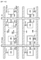
実施の形態1のカソード・パネルは、幹配線、枝配線及び電子放出部の模式的な平面的配置を図1に示すように、複数の幹配線20,22と、各幹配線から延びる複数の枝配線と、各枝配線に接続された電子放出部10とを具備する。複数の枝配線21は幹配線20から延びており、複数の枝配線23は幹配線22から延びている。幹配線20は第1の方向に延びており、幹配線22は第1の方向と異なる第2の方向(例えば、第1の方向と直角の方向)に延びている。電子放出部10は、各枝配線21,23に接続されている。例えばスピント型電界放出素子が形成された電子放出部10を備えたカソード・パネルを例にとると、電子放出部10を構成するカソード電極群は各枝配線21に接続されており、ゲート電極群は各枝配線23に接続されている。図1、また、後述する図4、図5においては、支持体や絶縁層の図示、電界放出素子の詳細な図示は省略した。幹配線、枝配線及び電子放出部の模式的な平面的配置を示す図面においては、幹配線及び枝配線を明確にするために、幹配線及び枝配線に斜線を付した。
【0081】
幹配線20及び枝配線21は、前述の[工程−100]において、例えばガラス基板から成る支持体51の上に、例えばポリシリコンから成るカソード電極用導電材料層をプラズマCVD法にて製膜した後、リソグラフィ技術及びドライエッチング技術に基づきカソード電極用導電材料層をパターニングして、カソード電極52を形成するときに、同時に形成すればよい。各電子放出部10を構成するカソード電極群を構成するパターニングされたカソード電極用導電材料層は、例えば矩形形状を有する。
【0082】
あるいは又、幹配線20及び枝配線21は、前述の[工程−210]において、第1絶縁層73の上に、例えばタングステンから成る電子放出層用導電材料層を製膜した後、リソグラフィ技術及びドライエッチング技術に基づき電子放出層用導電材料層をパターニングして、電子放出層74を形成するときに、同時に形成すればよい。
【0083】
あるいは又、幹配線20及び枝配線21は、前述の[工程−300]において、例えばガラス基板から成る支持体81の上に、例えばタングステンから成る電子放出層用導電材料層を製膜した後、リソグラフィ技術及びドライエッチング技術に基づき電子放出層用導電材料層をパターニングして、電子放出層84を形成するときに、同時に形成すればよい。
【0084】
一方、幹配線22及び枝配線23は、前述の[工程−100]において、ゲート電極用導電材料層をリソグラフィ技術及びドライエッチング技術にてパターニングすることによってゲート電極54を形成するときに、同時に形成すればよい。各電子放出部10を構成するゲート電極群を構成するパターニングされたゲート電極用導電材料層は、パターニングされたカソード電極用導電材料層と略同じ矩形形状を有する。
【0085】
あるいは又、幹配線22及び枝配線23は、前述の[工程−200]において、例えばガラス基板から成る支持体71の上に、例えばタングステンから成る第1ゲート電極用導電材料層を製膜した後、リソグラフィ技術及びドライエッチング技術に基づき第1ゲート電極用導電材料層をパターニングして、第1ゲート電極72を形成するときに、同時に形成すればよい。また、幹配線22及び枝配線23は、前述の[工程−220]において、第2絶縁層75の上に、例えばタングステンから成る第2ゲート電極用導電材料層を製膜した後、リソグラフィ技術及びドライエッチング技術に基づき第2ゲート電極用導電材料層をパターニングして、第2ゲート電極77を形成するときに、同時に形成すればよい。
【0086】
あるいは又、幹配線22及び枝配線23は、前述の[工程−300]において、絶縁層85の上に、例えばタングステンから成るゲート電極用導電材料層を製膜した後、リソグラフィ技術及びドライエッチング技術に基づきゲート電極用導電材料層をパターニングして、ゲート電極86を形成するときに、同時に形成すればよい。
【0087】
以上に説明した幹配線20,22及び枝配線21,23の形成方法は、以下に説明する実施の形態3及び実施の形態5における電界放出素子に対しても適用することができる。
【0088】
尚、図29の(A)に模式的な一部端面図を示し、図29の(B)に模式的な分解斜視図を示すように、所謂シャント構造を有する幹配線20,20’とすることもできる。即ち、[工程−100]において、例えばガラス基板から成る支持体51の上に、例えばポリシリコンから成るカソード電極用導電材料層をプラズマCVD法にて製膜した後、リソグラフィ技術及びドライエッチング技術に基づきカソード電極用導電材料層をパターニングして、カソード電極群、幹配線20及び枝配線21を形成する。その後、全面にSiO2から成る絶縁層53’をCVD法にて製膜し、幹配線20の上方の絶縁層53’に孔部を形成する。その後、孔部内を含む絶縁層53’上に例えばアルミニウム系合金層をスパッタ法にて製膜し、かかるアルミニウム系合金層をパターニングすることによって、絶縁層53’上にも幹配線20’を形成する。かかる幹配線20’は、孔部及び孔部に充填されたアルミニウム系合金層(これらを総称してコンタクトホールと呼ぶ)によって幹配線20と電気的に接続されている。次いで、全面に絶縁層53”を形成し、ゲート電極用導電材料層(例えば、TiN層)をスパッタ法にて、順次製膜し、次いで、ゲート電極用導電材料層をリソグラフィ技術及びドライエッチング技術にてパターニングすることによってゲート電極用導電材料層から成り、開口部55を有するゲート電極群を形成する。その後、絶縁層53”,53’に、例えば直径1μm程度の開口部55を形成する。
【0089】
また、図30の(A)に模式的な一部端面図を示し、図30の(B)に模式的な分解斜視図を示すように、支持体51上に幹配線20を形成せずに、絶縁層53’上にのみ幹配線20を形成し、コンタクトホールを介して、支持体51上に形成された枝配線21と幹配線20とを接続する構造とすることもできる。
【0090】
このように幹配線20をシャント構造にすることによって、信号の遅れ等の発生を回避することができる。これらのシャント構造は、エッジ型電界放出素子や平面型電界放出素子から構成された電子放出部10を備えたカソード・パネルに対しても適用することができる。
【0091】
得られたカソード・パネル50に対して、電子放出部10の動作試験(動作検査あるいは動作評価)を行う。動作試験として、電子放出部10の抵抗値や異常発熱を測定して短絡の有無を検査する配線短絡試験や、カソード・パネル50から実際に電子を放出させる表示特性試験を例示することができる。
【0092】
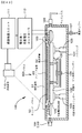
表示特性試験の実行に適した試験装置(検査装置あるいは評価装置)100の概要を図43に示す。この試験装置100は、上部が開口したハウジング101を具備する。ハウジング101内には、検査台102が配設されており、検査台102の下には検査台昇降シリンダー103が取り付けられている。検査台昇降シリンダー103は、図示しない移動台座に乗せられており、検査台102ごと図43の紙面垂直方向に移動可能である。検査台102の下には、更に、ピン昇降シリンダー104が取り付けられており、ピン昇降シリンダー104の作動によって検査台102を貫通した孔内をピン105が上下する。ハウジング101は、バルブ107を介して真空ポンプ(図示せず)に繋がれており、ハウジング101の雰囲気を高真空にすることができる。また、ガス流量制御装置108を介してハウジング101内にアルゴンガス等の不活性ガスを導入することができる構造となっている。ハウジング101内には、更に、幹配線20,22の端部に接触し得る構造の検査電圧印加針109が、例えば幹配線20,22の数だけ配置されている。
【0093】
ハウジング101の開口した上部には、透明基板61上に形成された蛍光体層62及びアノード電極63を有する、アノード・パネルと同様の構成を有するパネル60Aが配置されている。パネル60Aの上方にはCCDを有する受像装置110が配設されている。受像装置110は画像検査ユニット111に接続されている。また、電圧源・走査電圧コントローラ112が、画像検査ユニット111、検査電圧印加針109及びアノード電極63に接続されている。
【0094】
カソード・パネル50の動作試験に際しては、上昇位置にあるピン105上にカソード・パネル50を乗せ、ピン昇降シリンダー104を動作させることによってピン105を下降させて、カソード・パネル50を検査台102に載置する。そして、ハウジング101に設けられた扉(図示せず)を介して、検査台102に載置されたカソード・パネル50をハウジング101内に搬入した後、ハウジング101内を真空ポンプによって高真空雰囲気とする。尚、ガス流量制御装置108を介してハウジング101内にアルゴンガス等の不活性ガスを導入し、ハウジング101内の圧力を所定の値(例えば、1.2×10³Pa)に制御する。
【0095】
ハウジング101内が所望の雰囲気となったならば、検査台昇降シリンダー103を作動させて、検査台102を上昇させ、カソード・パネル50とパネル60Aとの間の距離を、例えば1mmとする。併せて、幹配線20,22の端部に検査電圧印加針109を接触させる。そして、電圧源・走査電圧コントローラ112から、検査電圧印加針109、幹配線20、枝配線21を介して電子放出部10のカソード電極52に走査用電圧(例えば、10ボルト)を印加し、検査電圧印加針109、幹配線22、枝配線23を介して電子放出部10のゲート電極54に制御用電圧(例えば、15ボルト)を印加し、更に、アノード電極63に加速用電圧(例えば、1.5kボルト)を印加する。これによって、電子放出電極56の先端部から電子が放出される。そして、電子は、パネル60Aに設けられたアノード電極63に引き付けられ、アノード電極63と透明基板61との間に形成された発光体層である蛍光体層62に衝突する。その結果、蛍光体層62が励起されて発光し、所望の画像を得ることができる。
【0096】
かかる画像を受像装置110にて受像し、受像装置110からの信号を画像検査ユニット111にて処理する。電子放出部10に欠陥がある場合、かかる電子放出部10に対応する画素に基づく画像には暗点や輝点、輝度ムラ等が発生する。このような画像異常を生じさせた電子放出部10(以下、動作不良の電子放出部10と呼ぶ)の位置を画像検査ユニット111にて解析し、図示しないディスプレイに表示する。あるいは、動作不良の電子放出部10の位置データを、後述する切断処理装置に送る。
【0097】
表示特性試験完了後、ハウジング101内の雰囲気を大気雰囲気とし、検査台昇降シリンダー103を作動させて、検査台102を下降させ、カソード・パネル50が載置された検査台102をハウジング101から搬出する。
【0098】
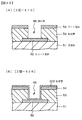
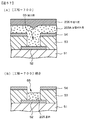
動作不良の電子放出部10に対しては、電子放出部10と幹配線20とを接続する枝配線21を切断する。あるいは又、電子放出部10と幹配線22とを接続する枝配線23を切断する。具体的には、図2に示すように、レーザを備えた切断処理装置において、レーザ光を用いて、電子放出部10と幹配線20とを接続する枝配線21を切断する。
【0099】
あるいは又、図3の(A)、(B)に示すように、カソード・パネル50の全面にレジスト層を塗布し、光ビームを用いてレジスト層を露光し、レジスト層を現像することによって、切断すべき枝配線23の部分を露出させる。そして、ドライエッチング法に基づき露出した枝配線23をエッチングすることによって切断した後、レジスト層を除去する(図3の(C)参照)。
【0100】
以上の処理が完了したカソード・パネル50とアノード・パネル60とを組み立てると、図27及び図28に示す表示装置を構成することができる。即ち、この表示装置は、基本的には、複数の画素から構成され、各画素は、カソード・パネル50上に設けられた電子放出部10と、電子放出部10に対向してアノード・パネル60上に設けられたアノード電極63及び蛍光体層62とから構成されている。以下の実施の形態における表示装置も同様の構成を有する。尚、図28は、カソード・パネル50及びアノード・パネル60の一部分の模式的な分解斜視図である。具体的には、セラミックスやガラスから作製された高さ約1mmの枠体を用意し、枠体とアノード・パネル60とをフリット・ガラスから成るシール材を用いて仮接着しておき、カソード・パネル50にフリット・ガラスから成るシール材を塗布・乾燥しておき、アノード・パネル60とカソード・パネル50とを枠体を介して張り合わせ、約450゜Cで10〜30分焼成すればよい。その後、表示装置の内部を10-4Pa程度の真空度となるまで排気し、適当な方法で封止する。あるいは又、真空室中でアノード・パネル60とカソード・パネル50とを枠体を介して張り合わせ、約450゜Cで10〜30分焼成すれば、アノード・パネル60とカソード・パネル50と枠体によって囲まれた空間は自ずから真空となる。尚、アノード・パネル60を構成する基板61は、少なくとも表面が絶縁性を有する材料から構成されていればよく、ガラス基板、表面に絶縁膜が形成されたガラス基板、石英基板、表面に絶縁膜が形成された石英基板、表面に絶縁膜が形成された半導体基板を挙げることができる。表示装置の構成に依存して、基板61には透明性を要求される場合がある。
【0101】
図1に示した構成では、1つの電子放出部10は、例えば数十乃至千個程度のスピント型電界放出素子から構成されている。パターニングされたカソード電極用導電材料層に、電子放出部10を構成するスピント型電界放出素子のカソード電極52が所望の数だけ存在している。具体的には、例えば矩形のカソード電極用導電材料層それ自体がカソード電極52に相当し、開口部55の底部に位置するカソード電極用導電材料層の領域がカソード電極52に該当する。また、パターニングされたゲート電極用導電材料層に、電子放出部10を構成するスピント型電界放出素子のゲート電極54が所望の数だけ存在している。具体的には、例えば矩形のゲート電極用導電材料層それ自体がゲート電極54に相当し、開口部55の近傍に位置するゲート電極用導電材料層の領域がゲート電極54に該当する。
【0102】
あるいは又、図1に示した構成では、1つの電子放出部10は、例えば数十乃至数百個程度のエッジ型電界放出素子から構成されている。図33(A)に示した構造を有するエッジ型電界放出素子から構成された1つの電子放出部10においては、パターニングされた電子放出層用導電材料層に、電子放出部10を構成するエッジ型電界放出素子の電子放出層74が所望の数だけ存在している。具体的には、例えば矩形の電子放出層用導電材料層それ自体が電子放出層74に相当し、開口部78の近傍に位置する電子放出層用導電材料層の領域が電子放出層74に該当する。更には、パターニングされたゲート電極用導電材料層に、電子放出部10を構成するエッジ型電界放出素子のゲート電極76が所望の数だけ存在している。具体的には、例えば矩形のゲート電極用導電材料層それ自体がゲート電極76に相当し、開口部78の近傍に位置するゲート電極用導電材料層の領域がゲート電極76に該当する。
【0103】
更には、図1に示した構成では、図33の(B)に示した構造を有するエッジ型電界放出素子から構成された1つの電子放出部10においては、パターニングされた第1ゲート電極用導電材料層に、電子放出部10を構成するエッジ型電界放出素子の第1ゲート電極72が所望の数だけ存在している。具体的には、例えば矩形の第1ゲート電極用導電材料層それ自体が第1ゲート電極72に相当し、開口部78の底部に位置する第1ゲート電極用導電材料層の領域が第1ゲート電極72に該当する。また、パターニングされた電子放出層用導電材料層に、電子放出部10を構成するエッジ型電界放出素子の電子放出層74が所望の数だけ存在している。具体的には、例えば矩形の電子放出層用導電材料層それ自体が電子放出層74に相当し、開口部78の近傍に位置する電子放出層用導電材料層の領域が電子放出層74に該当する。更には、パターニングされた第2ゲート電極用導電材料層に、電子放出部10を構成するエッジ型電界放出素子の第2ゲート電極77が所望の数だけ存在している。具体的には、例えば矩形の第2ゲート電極用導電材料層それ自体が第2ゲート電極77に相当し、開口部78の近傍に位置する第2ゲート電極用導電材料層の領域が第2ゲート電極77に該当する。
【0104】
あるいは又、図1に示した構成では、1つの電子放出部10は、例えば1つ若しくは複数の平面型電界放出素子から構成されている。図38に示した構造を有する平面型電界放出素子から構成された1つの電子放出部10においては、パターニングされた電子放出層用導電材料層に、電子放出部10を構成する平面型電界放出素子の電子放出層84が所望の数だけ存在している。具体的には、例えば矩形の電子放出層用導電材料層それ自体が電子放出層84に相当し、開口部88の底部に位置する電子放出層用導電材料層の領域が電子放出層84に該当する。更には、パターニングされたゲート電極用導電材料層に、電子放出部10を構成するエッジ型電界放出素子のゲート電極86が所望の数だけ存在している。具体的には、例えば矩形のゲート電極用導電材料層それ自体がゲート電極86に相当し、開口部88の近傍に位置するゲート電極用導電材料層の領域がゲート電極86に該当する。
【0105】
幹配線、枝配線及び電子放出部の変形例の模式的な平面的配置を図4及び図5に示す。
【0106】
図4に示す構成においては、パターニングされたカソード電極用導電材料層52Aに、電子放出部10を構成するスピント型電界放出素子のカソード電極52が所望の数だけ存在している。即ち、カソード電極用導電材料層52Aそれ自体がカソード電極52に相当し、開口部55の底部に位置するカソード電極用導電材料層52Aの領域がカソード電極52に該当する。カソード電極用導電材料層52Aは、図1に示した形状とは異なり、ストライプ状にパターニングされており、かかるストライプ状のカソード電極用導電材料層52Aの一部分(パターニングされたゲート電極用導電材料層と重複する領域)が、各電子放出部10のカソード電極52を構成する。言い換えれば、第1の方向に隣接する電子放出部10のカソード電極群はカソード電極延在部24によって結ばれている。一方、パターニングされたゲート電極用導電材料層に、電子放出部10を構成するスピント型電界放出素子のゲート電極54が所望の数だけ存在している。即ち、例えば矩形のゲート電極用導電材料層それ自体がゲート電極54に相当し、開口部55の近傍に位置するゲート電極用導電材料層の領域がゲート電極54に該当する。
【0107】
このように、図4に示すカソード・パネルにおいては、複数の電子放出部10が1次元的に配列されて成る冷陰極電界電子放出部列が、所定数、並置されている。ここで、複数の電子放出部10が1次元的に配列されているとは、ストライプ状のカソード電極用導電材料層52Aの一部分が各電子放出部10のカソード電極52を構成すること、あるいは又、或る方向に隣接する電子放出部10のカソード電極群がカソード電極延在部24によって結ばれていることを意味する。
【0108】
図4に示すカソード・パネルにおいては、図1に示したカソード・パネルと異なり、幹配線20及び枝配線21は省略されており、第1の方向に延びるストライプ状のカソード電極用導電材料層52Aが、これらの配線としての機能を果たす。幹配線22は第1の方向と異なる第2の方向(例えば、第1の方向と直角の方向)に延びている。電子放出部10を構成するゲート電極群は各枝配線23に接続されている。
【0109】
動作不良の電子放出部10に対しては、電子放出部10と幹配線22とを接続する枝配線23を切断すればよい。
【0110】
図5に示す構成においては、パターニングされたカソード電極用導電材料層に、電子放出部10を構成するスピント型電界放出素子のカソード電極52が所望の数だけ存在している。即ち、例えば矩形のカソード電極用導電材料層それ自体がカソード電極52に相当し、開口部55の底部に位置するカソード電極用導電材料層の領域がカソード電極52に該当する。一方、パターニングされたゲート電極用導電材料層に、電子放出部10を構成するスピント型電界放出素子のゲート電極54が所望の数だけ存在している。即ち、ゲート電極用導電材料層それ自体がゲート電極54に相当し、開口部55の近傍に位置するゲート電極用導電材料層の領域がゲート電極54に該当する。ゲート電極用導電材料層54Aは、図1に示した形状とは異なり、ストライプ状にパターニングされており、かかるストライプ状のゲート電極用導電材料層54Aの一部分(パターニングされたカソード電極用導電材料層と重複する領域)が、各電子放出部10のゲート電極54を構成する。言い換えれば、第2の方向に隣接する電子放出部10のゲート電極群はゲート電極延在部25によって結ばれている。
【0111】
このように、図5に示すカソード・パネルにおいては、複数の電子放出部10が1次元的に配列されて成る冷陰極電界電子放出部列が、所定数、並置されている。ここで、複数の電子放出部10が1次元的に配列されているとは、ストライプ状のゲート電極用導電材料層54Aの一部分が各電子放出部10のゲート電極54を構成すること、あるいは又、或る方向に隣接する電子放出部10のゲート電極群がゲート電極延在部25によって結ばれていることを意味する。
【0112】
図5に示すカソード・パネルにおいては、図1に示したカソード・パネルと異なり、幹配線22及び枝配線23は省略されており、第2の方向に延びるストライプ状のゲート電極用導電材料層54Aが、これらの配線としての機能を果たす。幹配線20は第2の方向と異なる第1の方向(例えば、第2の方向と直角の方向)に延びている。電子放出部10を構成するカソード電極群は各枝配線21に接続されている。
【0113】
動作不良の電子放出部10に対しては、電子放出部10と幹配線20とを接続する枝配線21を切断すればよい。
【0114】
第1の構造のエッジ型電界放出素子、第2の構造のエッジ型電界放出素子、及び平面型電界放出素子を有する電子放出部を備えたカソード・パネルに、図4及び図5に示した構成を適用したときの、各電極や電子放出層の構成や幹配線、枝配線の構成を以下の表1に纏めた。尚、記号「H」は幹配線及び枝配線が設けられている構成を表し、記号「S」は、電極や電子放出層がストライプ状のカソード電極用導電材料層あるいはゲート電極用導電材料層から構成されていることを表す。以下の表における記号「H」、「S」も同様の意味である。これらの構成においては、動作不良の電子放出部が動作しないように、動作不良の電子放出部と幹配線とを接続しているいずれかの枝配線を適宜切断すればよい。
【0115】

(実施の形態2)
実施の形態2は、本発明の第2の態様に係るカソード・パネル及び表示装置、並びに、カソード・パネルの製造方法に関する。
【0117】
電子放出部の構成は、前述した、複数(例えば、数十乃至千個程度)のスピント型電界放出素子、あるいは、複数(例えば、数十乃至数百個程度)のエッジ型電界放出素子、あるいは、1つ若しくは複数の平面型電界放出素子から構成することができる。以下、複数のスピント型電界放出素子から電子放出部が構成されている場合を例にとり、カソード・パネルを説明するが、他の電界放出素子から電子放出部が構成されている場合であっても実質的には同様である。
【0118】
実施の形態2のカソード・パネルも、幹配線、枝配線及び電子放出部の模式的な平面的配置を図6に示すように、複数の幹配線20,22(図6には、その内の1本を示す)と、各幹配線20,22から延びる複数の枝配線21,23と、各枝配線21,23に接続された電子放出部とを具備する。尚、図6には電子放出部の1つを示した。複数の枝配線21は幹配線20から延びており、複数の枝配線23は幹配線22から延びている。幹配線20は第1の方向に延びており、幹配線22は第1の方向と異なる第2の方向(例えば、第1の方向と直角の方向)に延びている。枝配線21は、幅の広い部分21aと、幅の狭い部分21bから構成されている。また、枝配線23は、幅の広い部分23aと、幅の狭い部分23bから構成されている。
【0119】
例えば100μm×180μmの寸法の各電子放出部は、1つあるいは複数(実施の形態2においては6つ)の冷陰極電界電子放出部ユニット(以下、電子放出部ユニットと呼ぶ)10aから構成されており、各電子放出部ユニット10aは枝配線21,23を介して幹配線20,22に接続されている。例えばスピント型電界放出素子が形成された電子放出部を備えたカソード・パネルを例にとると、電子放出部を構成するカソード電極群は各枝配線21に接続されており、ゲート電極群は各枝配線23に接続されている。図6においては、支持体や絶縁層の図示、電界放出素子の詳細な図示は省略した。
【0120】
幹配線20及び枝配線21は、前述の[工程−100]において、例えばガラス基板から成る支持体51の上に、例えばアルミニウム層から成るカソード電極用導電材料層をスパッタ法にて製膜した後、リソグラフィ技術及びドライエッチング技術に基づきカソード電極用導電材料層をパターニングして、カソード電極52を形成するときに、同時に形成すればよい。各電子放出部を構成するカソード電極群を構成するパターニングされたカソード電極用導電材料層は、例えば矩形形状を有する。尚、電界放出素子が完成した後、図7の(A)に模式的な一部端面図を示すように、枝配線21の少なくとも一部分、より具体的には、幅の狭い枝配線の部分21bの上方の絶縁層53をリソグラフィ技術及びドライエッチング技術に基づき除去しておく。この絶縁層53の一部の除去は、幹配線に走査回路との接続のためのパッド部を形成するときに、同時に行うことができる。
【0121】
あるいは又、幹配線20及び枝配線21は、前述の[工程−100]において、例えばガラス基板から成る支持体51の上に、例えばアルミニウム層52a及びTiNから成るバリアメタル層52bの2層から構成されたカソード電極用導電材料層をスパッタ法にて順次製膜した後、リソグラフィ技術及びドライエッチング技術に基づきカソード電極用導電材料層をパターニングして、カソード電極52を形成するときに、同時に形成すればよい。尚、電界放出素子が完成した後、枝配線21の少なくとも一部分の上方の絶縁層53及びバリアメタル層52bをリソグラフィ技術及びドライエッチング技術に基づき除去しておく。即ち、枝配線21を、アルミニウム層から成る第1の枝配線部分と、アルミニウム層とバリアメタル層の2層構造を有する第2の枝配線部分とから構成する。具体的には、完成した電界放出素子(図8の(A)参照)上にレジスト材料から成るエッチング用マスク(図示せず)をリソグラフィ技術に基づき形成した後、平行平板型RIE装置を用いて、以下の表2に例示する条件にて、SiO2から成る絶縁層53及びTiNから成るバリアメタル層52bをエッチングし、その後、エッチング用マスクを除去する(図8の(B)参照)。この絶縁層53及びバリアメタル層52bの一部の除去は、幹配線に走査回路との接続のためのパッド部を形成するときに、同時に行うことができる。
【0122】
[表2]
使用ガス :CHF3/CO/Ar=30/70/300sccm
圧力 :7.3Pa
RFパワー:1.3kW
温度 :20゜C
【0123】
あるいは又、幹配線20及び枝配線21は、前述の[工程−210]において、製膜技術及びドライエッチング技術に基づき、第1絶縁層73の上に幹配線20及び枝配線21を形成した後、電子放出層74を形成すればよい。あるいは又、幹配線20及び枝配線21は、前述の[工程−300]において、例えばガラス基板から成る支持体81の上に、製膜技術及びドライエッチング技術に基づき幹配線20及び枝配線21を形成した後、電子放出層84を形成すればよい。
【0124】
一方、幹配線22及び枝配線23は、前述の[工程−100]において、例えばアルミニウムから成るゲート電極用導電材料層をリソグラフィ技術及びドライエッチング技術にてパターニングすることによってゲート電極54を形成するときに、同時に形成すればよい。各電子放出部を構成するゲート電極群を構成するパターニングされたゲート電極用導電材料層は、パターニングされたカソード電極用導電材料層と略同じ矩形形状を有する。
【0125】
あるいは又、幹配線22及び枝配線23は、前述の[工程−100]において、例えば、厚さ0.5μmのアルミニウム層及び厚さ0.1μmのTiNから成るバリアメタル層の2層から構成されたゲート電極用導電材料層をリソグラフィ技術及びドライエッチング技術にてパターニングすることによってゲート電極54を形成するときに、同時に形成すればよい。尚、電界放出素子が完成した後、枝配線23の少なくとも一部分のバリアメタル層をリソグラフィ技術及びドライエッチング技術に基づき除去しておく。即ち、枝配線23を、アルミニウム層から成る第1の枝配線部分と、アルミニウム層とバリアメタル層の2層構造を有する第2の枝配線部分とから構成する。
【0126】
あるいは又、幹配線22及び枝配線23は、前述の[工程−200]において、例えばガラス基板から成る支持体71の上に、製膜技術及びドライエッチング技術に基づき幹配線22及び枝配線23を形成した後、第1ゲート電極72を形成すればよい。また、幹配線22及び枝配線23は、前述の[工程−220]において、第2絶縁層75の上に、製膜技術及びドライエッチング技術に基づき幹配線22及び枝配線23を形成した後、第2ゲート電極77を形成すればよい。あるいは又、幹配線22及び枝配線23は、前述の[工程−300]において、絶縁層85の上に、製膜技術及びドライエッチング技術に基づき幹配線22及び枝配線23を形成した後、ゲート電極86を形成すればよい。
【0127】
尚、枝配線21と枝配線23の内の少なくとも一方が、アルミニウム層あるいはアルミニウム合金層から構成され、あるいは又、アルミニウム層あるいはアルミニウム合金層から成る第1の枝配線部分と、アルミニウム層あるいはアルミニウム合金層とバリアメタル層の2層構造を有する第2の枝配線部分とから構成されていればよい。
【0128】
以上の幹配線20,22の形成方法、枝配線21,23の形成方法を、後述する実施の形態4及び実施の形態6に適用することができる。
【0129】
実施の形態2においては、純度99.99%のアルミニウム層から成る枝配線21,23の幅の狭い部分21b,23bの幅を2μm、厚さを0.5μm、長さを0.1mm以上とする。また、純度99.99%のアルミニウム層から成る幹配線20,22、枝配線21,23の幅の広い部分21a,23aの幅を20μm、厚さを0.5μmとする。枝配線21,23の幅の狭い部分21b,23bの電気抵抗値Rは以下のとおりである。尚、アルミニウム層の体積抵抗率ρを2.7×10⁻⁶(Ω・cm)とし、枝配線21,23の幅の狭い部分21b,23bの断面積をA、長さをLとする。
【0130】
従って、L=0.5mmとすれば、R=13.5Ωとなる。
【0132】
得られたカソード・パネル50に対して、幹配線20,22から枝配線21,23を介して電子放出部に電圧を印加する短絡試験を行う。具体的には、幹配線20と幹配線22との間に10ボルト(=E)の電位差を与える。電位差は連続的に与えてもよいし、パルス状に与えてもよい。短絡が生じている電子放出部、即ち、例えばゲート電極54と電子放出電極56との間に導電性の異物が存在している電界放出素子を含む電子放出部にあっては、かかる電子放出部と幹配線20,22とを接続する枝配線21,23を、枝配線21,23を流れる電流Iによって断線させる(図7の(B)の模式的な一部端面図を参照)。尚、枝配線21,23の幅の狭い部分21b,23bの断線は、いずれか一方あるいは両方に生じ得る。ここで、枝配線21,23の幅の狭い部分21b,23bを流れる電流Iの電流密度Jは以下のとおりとなる。
【0133】
このような条件で枝配線の幅の狭い部分21b,23bがエレクトロマイグレーションに起因して断線するまでの時間を調べた結果を、図9に示す。尚、試験雰囲気は大気雰囲気である。図9から、約1時間、幹配線20と幹配線22との間に10ボルトの電位差を与え続けることによって、短絡が生じている電子放出部と幹配線とを接続する枝配線がほぼ全て断線することが判る。尚、試験雰囲気を不活性ガス雰囲気とし、電子放出部、幹配線20,22や枝配線21,23を加熱した状態で短絡試験を行えば、短絡が生じている電子放出部と幹配線とを接続する枝配線が断線するまでの時間の短縮化を図ることができる。
【0135】
実施の形態2においては、各電子放出部を複数(例えば6つ)の電子放出部ユニット10aから構成すれば、例えば1つの電子放出部ユニット10aにおける枝配線が断線されても、残りの電子放出部ユニット10aが機能するので、外見上は遜色のない画素を得ることができる。
【0136】
以上の処理が完了したカソード・パネル50とアノード・パネル60とを組み立てると、図27に示した表示装置を構成することができる。
【0137】
尚、場合によっては、カソード・パネル50とアノード・パネル60とを組み立てた後に、短絡試験を行い、短絡状態にある電子放出部と幹配線とを接続する枝配線を断線させてもよい。
【0138】
幹配線、枝配線及び電子放出部の変形例としては、図4及び図5の模式的な平面的配置に示したと同様の構成を挙げることができる。
【0139】
(実施の形態3)
実施の形態3は、本発明の第3の態様に係るカソード・パネル及び表示装置、並びに、カソード・パネルの製造方法に関する。
【0140】
電子放出部の構成は、前述した、複数(例えば、数十乃至千個程度)のスピント型電界放出素子、あるいは、複数(例えば、数十乃至数百個程度)のエッジ型電界放出素子、あるいは、1つ若しくは複数の平面型電界放出素子から構成することができる。以下、複数のスピント型電界放出素子から電子放出部が構成されている場合を例にとり、カソード・パネルを説明するが、他の電界放出素子から電子放出部が構成されている場合であっても実質的には同様である。
【0141】
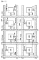
実施の形態3のカソード・パネルは、幹配線、枝配線及び電子放出部の模式的な平面的配置を図10に示すように、複数の幹配線30,32と、各幹配線30,32から延びる、複数の第1枝配線31A,33A及び複数の第2枝配線31B,33Bと、複数の冷陰極電界電子放出領域(以下、単に、電子放出領域と呼ぶ)とを具備する。複数の第1枝配線31A及び第2枝配線31Bは幹配線30から延びており、複数の第1枝配線33A及び第2枝配線33Bは幹配線32から延びている。幹配線30は第1の方向に延びており、幹配線32は第1の方向と異なる第2の方向(例えば、第1の方向と直角の方向)に延びている。尚、図10、また、後述する図11〜図17においては、支持体や絶縁層の図示、電界放出素子の詳細な図示は省略した。
【0142】
各電子放出領域は、幹配線30,32から延びる第1枝配線31A,33Aに接続された第1冷陰極電界電子放出部10A(以下、第1電子放出部10Aと呼ぶ)、及び、該幹配線30,32から延びる第2枝配線31B,33Bに接続された第2冷陰極電界電子放出部10B(以下、第2電子放出部10Bと呼ぶ)から構成されている。具体的には、第1電子放出部10Aを構成するカソード電極群は、第1枝配線31Aを介して幹配線30に接続されており、第1電子放出部10Aを構成するゲート電極群は、第1枝配線33Aを介して幹配線32に接続されている。一方、第2電子放出部10Bを構成するカソード電極群は、第2枝配線31Bを介して幹配線30に接続されており、第2電子放出部10Bを構成するゲート電極群は、第2枝配線33Bを介して幹配線32に接続されている。そして、電子放出領域を構成する一方の電子放出部(例えば、第1電子放出部10A)が動作不良である場合、この一方の電子放出部(例えば、第1電子放出部10A)と幹配線30,32とを接続する枝配線(例えば、第1枝配線31Aあるいは第1枝配線33A)は切断されている。一方、電子放出領域を構成する両方の電子放出部(第1電子放出部10A及び第2電子放出部10B)の動作が正常な場合、この電子放出領域を構成するいずれか一方の電子放出部(例えば、第2電子放出部10B)と幹配線30,32とを接続する枝配線(例えば、第2枝配線31Bあるいは第2枝配線33B)は切断されている。
【0143】
このように、電子放出領域を一対の電子放出部10A,10Bから構成し、第1電子放出部10A及び第2電子放出部10Bのいずれか一方を動作させることによって、表示装置の輝度を一定に保つことができる。
【0144】
幹配線30及び第1枝配線31A、第2枝配線31Bは、実施の形態1における幹配線20及び枝配線21と同様に形成することができるし、幹配線32及び第1枝配線33A、第2枝配線33Bは、実施の形態1における幹配線22及び枝配線23と同様に形成することができるので、詳細な説明は省略する。
【0145】
得られたカソード・パネル50に対して、第1及び第2電子放出部10A,10Bの動作試験を行う。動作試験として、これらの電子放出部の抵抗値や異常発熱を測定して短絡の有無を検査する配線短絡試験や、カソード・パネル50から実際に電子を放出させる表示特性試験を例示することができる。表示特性試験においては、一対の電子放出部10A,10Bが正常な動作をする場合、一対の電子放出部10A,10Bのいずれか一方が動作不良である場合と比較して、画素に対応する画像は明るい。
【0146】
動作不良の電子放出領域に対しては、例えば、第1電子放出部10Aと幹配線30とを接続する枝配線31Aを切断する。あるいは又、第1電子放出部10Aと幹配線32とを接続する枝配線33Aを切断する。一方、動作が正常の電子放出領域に対しては、例えば、第2電子放出部10Bと幹配線30とを接続する枝配線31Bを切断する。あるいは又、第2電子放出部10Bと幹配線32とを接続する枝配線33Bを切断する。具体的には、実施の形態1と同様の方法を実行すればよい。
【0147】
以上の処理が完了したカソード・パネル50とアノード・パネル60とを組み立てると、図27に示した表示装置を構成することができる。
【0148】
幹配線、枝配線及び電子放出部の変形例の模式的な平面的配置を図11〜図17に示す。
【0149】
図11に示す構成においては、カソード電極用導電材料層52Aは、図10に示した形状とは異なり、ストライプ状にパターニングされており、かかるストライプ状のカソード電極用導電材料層52Aの一部分(パターニングされたゲート電極用導電材料層と重複する領域)が、各電子放出部10A,10Bのカソード電極52を構成する。言い換えれば、第1の方向に隣接する電子放出部10A,10Bのカソード電極群はカソード電極延在部34によって結ばれており、複数の電子放出部10A,10Bが1次元的に第1の方向に配列されている。図11に示すカソード・パネルにおいては、図10に示したカソード・パネルと異なり、幹配線30及び枝配線31A,31Bは省略されており、第1の方向に延びるストライプ状のカソード電極用導電材料層52Aが、これらの配線としての機能を果たす。幹配線32は第1の方向と異なる第2の方向(例えば、第1の方向と直角の方向)に延びている。電子放出部10A,10Bを構成するゲート電極群は各枝配線33A,33Bに接続されている。
【0150】
動作不良の電子放出領域に対しては、例えば、第1電子放出部10Aと幹配線32とを接続する第1枝配線33Aを切断すればよい。一方、正常な動作を示す電子放出領域に対しては、例えば、第2電子放出部10Bと幹配線32とを接続する第2枝配線33Bを切断すればよい。
【0151】
図12に示す構成においては、ゲート電極用導電材料層54Aは、図10に示した形状とは異なり、ストライプ状にパターニングされており、かかるストライプ状のゲート電極用導電材料層54Aの一部分(パターニングされたカソード電極用導電材料層と重複する領域)が、各電子放出部10A,10Bのゲート電極54を構成する。言い換えれば、第2の方向に隣接する電子放出部10A,10Bのゲート電極群はゲート電極延在部35によって結ばれており、複数の電子放出部10A,10Bが1次元的に第2の方向に配列されている。図12に示すカソード・パネルにおいては、図10に示したカソード・パネルと異なり、幹配線32及び枝配線33A,33Bは省略されており、第2の方向に延びるストライプ状のゲート電極用導電材料層54Aが、これらの配線としての機能を果たす。幹配線30は第2の方向と異なる第1の方向(例えば、第2の方向と直角の方向)に延びている。電子放出部10A,10Bを構成するカソード電極群は各枝配線31A,31Bに接続されている。
【0152】
動作不良の電子放出領域に対しては、例えば、第1電子放出部10Aと幹配線30とを接続する第1枝配線31Aを切断すればよい。一方、正常な動作を示す電子放出領域に対しては、例えば、第2電子放出部10Bと幹配線30とを接続する第2枝配線31Bを切断すればよい。
【0153】
図13に示す構成においては、第2の方向に延びる幹配線が一対の幹配線32A,32Bから構成されている。第1電子放出部10Aを構成するカソード電極群は、第1枝配線31Aを介して幹配線30に接続されており、第1電子放出部10Aを構成するゲート電極群は、第1枝配線33Aを介して幹配線32Aに接続されている。一方、第2電子放出部10Bを構成するカソード電極群は、第2枝配線31Bを介して幹配線30に接続されており、第2電子放出部10Bを構成するゲート電極群は、第2枝配線33Bを介して幹配線32Bに接続されている。このような構成にすることによって、第1電子放出部10A及び第2電子放出部10Bを独立して動作させることが可能となる。
【0154】
得られたカソード・パネル50に対して、第1及び第2電子放出部10A,10Bの動作試験を行う。動作試験として、これらの電子放出部の抵抗値や異常発熱を測定して短絡の有無を検査する配線短絡試験や、カソード・パネル50から実際に電子を放出させる表示特性試験を例示することができる。表示特性試験においては、幹配線30と幹配線32Aに電圧を印加することによって、第1電子放出部10Aの動作試験を行う。次いで、幹配線30と幹配線32Bに電圧を印加することによって、第2電子放出部10Bの動作試験を行う。
【0155】
動作不良の電子放出領域に対しては、動作不良が生じた第1若しくは第2電子放出部10A,10Bと幹配線30とを接続する枝配線31A若しくは枝配線31Bを切断する。あるいは又、動作不良が生じた第1若しくは第2電子放出部10A,10Bと幹配線32A,32Bとを接続する枝配線33A若しくは枝配線33Bを切断する。一方、動作が正常の電子放出領域に対しては、第1電子放出部10A及び第2電子放出部10Bのいずれか一方と幹配線30とを接続する枝配線31A,31Bを切断する。あるいは又、第1電子放出部10A及び第2電子放出部10Bのいずれか一方と幹配線32A,32Bとを接続する枝配線33A,33Bを切断する。即ち、動作が正常の電子放出領域に対しては、第1電子放出部10A及び第2電子放出部10Bのいずれか一方を、動作しない状態とすればよい。具体的には、実施の形態1と同様の方法を実行すればよい。これによって、第1電子放出部10A及び第2電子放出部10Bのいずれか一方のみが動作する結果、表示装置の輝度を一定に保つことができる。尚、一対の幹配線32A,32Bにおいて、幹配線32Aに接続された全ての電子放出部10Aが正常な動作をし、幹配線32Bに接続された全ての電子放出部10Bが正常な動作をする場合には、場合によっては、一方の幹配線を電子放出部を駆動するための電源に接続しない構成とすることもできるし、あるいは又、かかる一方の幹配線を切断してもよい。また、幹配線32Aに接続された全ての電子放出部10Aが正常な動作をし、幹配線32Bに接続された少なくとも1つの電子放出部10Bが動作不良を示す場合には、場合によっては、幹配線32Bを電子放出部を駆動するための電源に接続しない構成とすることもできるし、あるいは又、かかる幹配線32Bを切断してもよい。あるいは、幹配線32Aに接続された少なくとも1つの電子放出部10Aが動作不良を示し、幹配線32Bに接続された全ての電子放出部10Bが正常な動作を行う場合には、場合によっては、幹配線32Aを電子放出部を駆動するための電源に接続しない構成とすることもできるし、あるいは又、幹配線32Aを切断してもよい。
【0156】
図14に示す構成は、図13に示した構成と図11に示した構成の組合せである。即ち、図14に示す構成においては、カソード電極用導電材料層52Aは、図13に示した形状とは異なり、ストライプ状にパターニングされており、かかるストライプ状のカソード電極用導電材料層52Aの一部分(パターニングされたゲート電極用導電材料層と重複する領域)が、各電子放出部10A,10Bのカソード電極52を構成する。言い換えれば、第1の方向に隣接する電子放出部10A,10Bのカソード電極群はカソード電極延在部34によって結ばれており、複数の電子放出部10A,10Bが1次元的に第1の方向に配列されている。図14に示すカソード・パネルにおいては、図13に示したカソード・パネルと異なり、幹配線30及び枝配線31A,31Bは省略されており、第1の方向に延びるストライプ状のカソード電極用導電材料層52Aが、これらの配線としての機能を果たす。幹配線32A,32Bは第1の方向と異なる第2の方向(例えば、第1の方向と直角の方向)に延びている。第1電子放出部10Aを構成するゲート電極群は枝配線33Aを介して幹配線32Aに接続されている。一方、第2電子放出部10Bを構成するゲート電極群は枝配線33Bを介して幹配線32Bに接続されている。
【0157】
動作不良の電子放出領域に対しては、動作不良が生じた第1若しくは第2電子放出部10A,10Bと幹配線32A,32Bとを接続する枝配線33A若しくは枝配線33Bを切断すればよい。一方、動作が正常の電子放出領域に対しては、第1電子放出部10A及び第2電子放出部10Bのいずれか一方と幹配線32A,32Bとを接続する枝配線33A,33Bを切断すればよい。即ち、動作が正常の電子放出領域に対しては、第1電子放出部10A及び第2電子放出部10Bのいずれか一方を、動作しない状態とすればよい。尚、一対の幹配線32A,32Bにおいて、幹配線32Aに接続された全ての電子放出部10Aが正常な動作をし、幹配線32Bに接続された全ての電子放出部10Bが正常な動作をする場合には、場合によっては、一方の幹配線を電子放出部を駆動するための電源に接続しない構成とすることもできるし、あるいは又、かかる一方の幹配線を切断してもよい。また、幹配線32Aに接続された全ての電子放出部10Aが正常な動作をし、幹配線32Bに接続された少なくとも1つの電子放出部10Bが動作不良を示す場合には、場合によっては、幹配線32Bを電子放出部を駆動するための電源に接続しない構成とすることもできるし、あるいは又、かかる幹配線32Bを切断してもよい。あるいは、幹配線32Aに接続された少なくとも1つの電子放出部10Aが動作不良を示し、幹配線32Bに接続された全ての電子放出部10Bが正常な動作を行う場合には、場合によっては、幹配線32Aを電子放出部を駆動するための電源に接続しない構成とすることもできるし、あるいは又、幹配線32Aを切断してもよい。
【0158】
図15に示す構成においては、第1の方向に延びる幹配線が一対の幹配線30A,30Bから構成されている。第1電子放出部10Aを構成するカソード電極群は、第1枝配線31Aを介して幹配線30Aに接続されており、第1電子放出部10Aを構成するゲート電極群は、第1枝配線33Aを介して幹配線32に接続されている。一方、第2電子放出部10Bを構成するカソード電極群は、第2枝配線31Bを介して幹配線30Bに接続されており、第2電子放出部10Bを構成するゲート電極群は、第2枝配線33Bを介して幹配線32に接続されている。このような構成にすることによっても、第1電子放出部10A及び第2電子放出部10Bを独立して動作させることが可能となる。
【0159】
得られたカソード・パネル50に対して、第1及び第2電子放出部10A,10Bの動作試験を行う。動作試験として、これらの電子放出部の抵抗値や異常発熱を測定して短絡の有無を検査する配線短絡試験や、カソード・パネル50から実際に電子を放出させる表示特性試験を例示することができる。表示特性試験においては、幹配線32と幹配線30Aに電圧を印加することによって、第1電子放出部10Aの動作試験を行う。次いで、幹配線32と幹配線30Bに電圧を印加することによって、第2電子放出部10Bの動作試験を行う。
【0160】
動作不良の電子放出領域に対しては、動作不良が生じた第1若しくは第2電子放出部10A,10Bと幹配線30A,30Bとを接続する枝配線31A若しくは枝配線31Bを切断する。あるいは又、動作不良が生じた第1若しくは第2電子放出部10A,10Bと幹配線32とを接続する枝配線33A若しくは枝配線33Bを切断する。一方、動作が正常の電子放出領域に対しては、第1電子放出部10A及び第2電子放出部10Bのいずれか一方と幹配線30A,30Bとを接続する枝配線31A,31Bを切断する。あるいは又、第1電子放出部10A及び第2電子放出部10Bのいずれか一方と幹配線32とを接続する枝配線33A,33Bを切断する。即ち、動作が正常の電子放出領域に対しては、第1電子放出部10A及び第2電子放出部10Bのいずれか一方を、動作しない状態とすればよい。具体的には、実施の形態1と同様の方法を実行すればよい。尚、一対の幹配線30A,30Bにおいて、幹配線30Aに接続された全ての電子放出部10Aが正常な動作をし、幹配線30Bに接続された全ての電子放出部10Bが正常な動作をする場合には、場合によっては、一方の幹配線を電子放出部を駆動するための電源に接続しない構成とすることもできるし、あるいは又、かかる一方の幹配線を切断してもよい。また、幹配線30Aに接続された全ての電子放出部10Aが正常な動作をし、幹配線30Bに接続された少なくとも1つの電子放出部10Bが動作不良を示す場合には、場合によっては、幹配線30Bを電子放出部を駆動するための電源に接続しない構成とすることもできるし、あるいは又、幹配線30Bを切断してもよい。あるいは、幹配線30Aに接続された少なくとも1つの電子放出部10Aが動作不良を示し、幹配線30Bに接続された全ての電子放出部10Bが正常な動作を行う場合には、場合によっては、幹配線30Aを電子放出部を駆動するための電源に接続しない構成とすることもできるし、あるいは又、幹配線30Aを切断してもよい。
【0161】
図16に示す構成は、図15に示した構成と図12に示した構成の組合せである。即ち、図16に示す構成においては、ゲート電極用導電材料層54Aは、図15に示した形状とは異なり、ストライプ状にパターニングされており、かかるストライプ状のゲート電極用導電材料層54Aの一部分(パターニングされたカソード電極用導電材料層と重複する領域)が、各電子放出部10A,10Bのゲート電極54を構成する。言い換えれば、第2の方向に隣接する電子放出部10A,10Bのゲート電極群はゲート電極延在部35によって結ばれており、複数の電子放出部10A,10Bが1次元的に第2の方向に配列されている。図16に示すカソード・パネルにおいては、図15に示したカソード・パネルと異なり、幹配線32及び枝配線33A,33Bは省略されており、第2の方向に延びるストライプ状のゲート電極用導電材料層54Aが、これらの配線としての機能を果たす。幹配線30A,30Bは第2の方向と異なる第1の方向(例えば、第2の方向と直角の方向)に延びている。第1電子放出部10Aを構成するカソード電極群は枝配線31Aを介して幹配線30Aに接続されている。一方、第2電子放出部10Bを構成するカソード電極群は枝配線31Bを介して幹配線30Bに接続されている。
【0162】
動作不良の電子放出領域に対しては、動作不良が生じた第1若しくは第2電子放出部10A,10Bと幹配線30A,30Bとを接続する枝配線31A若しくは枝配線31Bを切断すればよい。一方、動作が正常の電子放出領域に対しては、第1電子放出部10A及び第2電子放出部10Bのいずれか一方と幹配線30A,30Bとを接続する枝配線31A,31Bを切断すればよい。即ち、動作が正常の電子放出領域に対しては、第1電子放出部10A及び第2電子放出部10Bのいずれか一方を、動作しない状態とすればよい。尚、一対の幹配線30A,30Bにおいて、幹配線30Aに接続された全ての電子放出部10Aが正常な動作をし、幹配線30Bに接続された全ての電子放出部10Bが正常な動作をする場合には、場合によっては、一方の幹配線を電子放出部を駆動するための電源に接続しない構成とすることもできるし、あるいは又、かかる一方の幹配線を切断してもよい。また、幹配線30Aに接続された全ての電子放出部10Aが正常な動作をし、幹配線30Bに接続された少なくとも1つの電子放出部10Bが動作不良を示す場合には、場合によっては、幹配線30Bを電子放出部を駆動するための電源に接続しない構成とすることもできるし、あるいは又、かかる幹配線30Bを切断してもよい。あるいは、幹配線30Aに接続された少なくとも1つの電子放出部10Aが動作不良を示し、幹配線30Bに接続された全ての電子放出部10Bが正常な動作を行う場合には、場合によっては、幹配線30Aを電子放出部を駆動するための電源に接続しない構成とすることもできるし、あるいは又、幹配線30Aを切断してもよい。
【0163】
図17に示す構成においては、第1の方向に延びる幹配線が一対の幹配線30A,30Bから構成されており、且つ、第2の方向に延びる幹配線が一対の幹配線32A,32Bから構成されている。第1電子放出部10Aを構成するカソード電極群は、第1枝配線31Aを介して幹配線30Aに接続されており、第1電子放出部10Aを構成するゲート電極群は、第1枝配線33Aを介して幹配線32Aに接続されている。一方、第2電子放出部10Bを構成するカソード電極群は、第2枝配線31Bを介して幹配線30Bに接続されており、第2電子放出部10Bを構成するゲート電極群は、第2枝配線33Bを介して幹配線32Bに接続されている。このような構成にすることによっても、第1電子放出部10A及び第2電子放出部10Bを独立して動作させることが可能となる。
【0164】
得られたカソード・パネル50に対して、第1及び第2電子放出部10A,10Bの動作試験を行う。動作試験として、これらの電子放出部の抵抗値や異常発熱を測定して短絡の有無を検査する配線短絡試験や、カソード・パネル50から実際に電子を放出させる表示特性試験を例示することができる。表示特性試験においては、幹配線30Aと幹配線32Aに電圧を印加することによって、第1電子放出部10Aの動作試験を行う。次いで、幹配線30Bと幹配線32Bに電圧を印加することによって、第2電子放出部10Bの動作試験を行う。
【0165】
動作不良の電子放出領域に対しては、動作不良が生じた第1若しくは第2電子放出部10A,10Bと幹配線30A,30Bとを接続する枝配線31A若しくは枝配線31Bを切断する。あるいは又、動作不良が生じた第1若しくは第2電子放出部10A,10Bと幹配線32A,32Bとを接続する枝配線33A若しくは枝配線33Bを切断する。一方、動作が正常の電子放出領域に対しては、第1電子放出部10A及び第2電子放出部10Bのいずれか一方と幹配線30A,30Bとを接続する枝配線31A,31Bを切断する。あるいは又、第1電子放出部10A及び第2電子放出部10Bのいずれか一方と幹配線32A,32Bとを接続する枝配線33A,33Bを切断する。即ち、動作が正常の電子放出領域に対しては、第1電子放出部10A及び第2電子放出部10Bのいずれか一方を、動作しない状態とすればよい。具体的には、実施の形態1と同様の方法を実行すればよい。尚、対の幹配線30A,30B,32A,32Bにおいて、幹配線30A,32Aに接続された全ての電子放出部10Aが正常な動作をし、幹配線30B,32Bに接続された全ての電子放出部10Bが正常な動作をする場合には、場合によっては、いずれか1つの幹配線を電子放出部を駆動するための電源に接続しない構成とすることもできるし、あるいは又、かかるいずれか1つの幹配線を切断してもよい。また、幹配線30A,32Aに接続された全ての電子放出部10Aが正常な動作をし、幹配線30B,32Bに接続された少なくとも1つの電子放出部10Bが動作不良を示す場合には、場合によっては、幹配線30B、幹配線32Bの少なくとも一方を電子放出部を駆動するための電源に接続しない構成とすることもできるし、あるいは又、幹配線30B,32Bの少なくとも一方を切断してもよい。あるいは、幹配線30A,32Aに接続された少なくとも1つの電子放出部10Aが動作不良を示し、幹配線30B,32Bに接続された全ての電子放出部10Bが正常な動作を行う場合には、場合によっては、幹配線30A、幹配線32Aの少なくとも一方を電子放出部を駆動するための電源に接続しない構成とすることもできるし、あるいは又、幹配線30A,32Aの少なくとも一方を切断してもよい。
【0166】
第1の構造のエッジ型電界放出素子、第2の構造のエッジ型電界放出素子、及び平面型電界放出素子を有する電子放出部を備えたカソード・パネルに、図11、図12、図14、図16に示した構成を適用したときの、各電極や電子放出層の構成や幹配線、枝配線の構成は表1に示したと同様である。
【0167】
(実施の形態4)
実施の形態4は、本発明の第4の態様に係るカソード・パネル及び表示装置、並びに、カソード・パネルの製造方法に関する。
【0168】
電子放出部の構成は、前述した、複数(例えば、数十乃至千個程度)のスピント型電界放出素子、あるいは、複数(例えば、数十乃至数百個程度)のエッジ型電界放出素子、あるいは、1つ若しくは複数の平面型電界放出素子から構成することができる。以下、複数のスピント型電界放出素子から電子放出部が構成されている場合を例にとり、カソード・パネルを説明するが、他の電界放出素子から電子放出部が構成されている場合であっても実質的には同様である。
【0169】
実施の形態4のカソード・パネルは、幹配線、枝配線及び電子放出部の模式的な平面的配置を図10に示したと同様に、複数の幹配線30,32と、各幹配線30,32から延びる、複数の第1枝配線31A,33A及び複数の第2枝配線31B,33Bと、複数の電子放出領域とを具備する。複数の第1枝配線31A及び第2枝配線31Bは幹配線30から延びており、複数の第1枝配線33A及び第2枝配線33Bは幹配線32から延びている。幹配線30は第1の方向に延びており、幹配線32は第1の方向と異なる第2の方向(例えば、第1の方向と直角の方向)に延びている。
【0170】
各電子放出領域は、幹配線30,32から延びる第1枝配線31A,33Aに接続された第1電子放出部10A、及び、該幹配線30,32から延びる第2枝配線31B,33Bに接続された第2電子放出部10Bから構成されている。具体的には、第1電子放出部10Aを構成するカソード電極群は、第1枝配線31Aを介して幹配線30に接続されており、第1電子放出部10Aを構成するゲート電極群は、第1枝配線33Aを介して幹配線32に接続されている。一方、第2電子放出部10Bを構成するカソード電極群は、第2枝配線31Bを介して幹配線30に接続されており、第2電子放出部10Bを構成するゲート電極群は、第2枝配線33Bを介して幹配線32に接続されている。そして、電子放出領域を構成する一方の電子放出部(例えば、第1電子放出部10A)が動作不良である場合、この一方の電子放出部(例えば、第1電子放出部10A)と幹配線30,32とを接続する枝配線(例えば、第1枝配線31Aあるいは第1枝配線33A)は断線している。一方、電子放出領域を構成する両方の電子放出部(第1電子放出部10A及び第2電子放出部10B)の動作が正常な場合、この電子放出領域を構成するいずれか一方の電子放出部(例えば、第2電子放出部10B)と幹配線30,32とを接続する枝配線(例えば、第2枝配線31Bあるいは第2枝配線33B)は切断されている。尚、第1電子放出部10A、第2電子放出部10Bの構成は、例えば、実施の形態1や実施の形態2における電子放出部と同様の構成とすればよい。
【0171】
このように、電子放出領域を一対の電子放出部10A,10Bから構成し、第1電子放出部10A及び第2電子放出部10Bのいずれか一方を動作させることによって、表示装置の輝度を一定に保つことができる。
【0172】
幹配線30及び第1枝配線31A、第2枝配線31Bは、実施の形態2における幹配線20及び枝配線21と同様に形成することができるし、幹配線32及び第1枝配線33A、第2枝配線33Bは、実施の形態2における幹配線22及び枝配線23と同様に形成することができるので、詳細な説明は省略する。
【0173】
得られたカソード・パネル50に対して、実施の形態2にて説明したと同様に、第1及び第2電子放出部10A,10Bの短絡試験を行う。短絡状態にある電子放出領域においては、電子放出領域を構成し、且つ、短絡状態にある電子放出部と幹配線とを接続する枝配線を、枝配線を流れる電流によって断線させる。一方、短絡状態にない動作が正常の電子放出領域においては、電子放出領域を構成するいずれか一方の電子放出部と幹配線とを接続する枝配線を、実施の形態1と同様の方法を実行することによって切断する。尚、短絡試験を行った後、実施の形態3と同様に、表示特性試験を行うことが好ましい。表示特性試験においては、一対の電子放出部10A,10Bが正常な動作をする場合、一対の電子放出部10A,10Bのいずれか一方が動作不良である場合と比較して、画素に対応する画像は明るい。従って、かかる一対の電子放出部10A,10Bのいずれか一方の電子放出部と幹配線とを接続する枝配線を、実施の形態1と同様の方法を実行することによって切断すればよい。
【0174】
以上の処理が完了したカソード・パネル50とアノード・パネル60とを組み立てると、図27に示した表示装置を構成することができる。
【0175】
幹配線、枝配線及び電子放出部の変形例としては、図11〜図17の模式的な平面的配置に示したと同様の構成を挙げることができる。
【0176】
(実施の形態5)
実施の形態5は、本発明の第5の態様に係るカソード・パネル及び表示装置、並びに、カソード・パネルの製造方法に関する。
【0177】
電子放出部の構成は、前述した、複数(例えば、数十乃至千個程度)のスピント型電界放出素子、あるいは、複数(例えば、数十乃至数百個程度)のエッジ型電界放出素子、あるいは、1つ若しくは複数の平面型電界放出素子から構成することができる。以下、複数のスピント型電界放出素子から電子放出部が構成されている場合を例にとり、カソード・パネルを説明するが、他の電界放出素子から電子放出部が構成されている場合であっても実質的には同様である。
【0178】
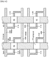
実施の形態5のカソード・パネルは、幹配線、枝配線及び電子放出部の模式的な平面的配置を図18に示すように、複数の幹配線30,32と、各幹配線30,32から延びる複数の枝配線31A,31B,33と、複数の電子放出領域とを具備する。複数の枝配線31A,枝配線31Bは幹配線30から延びており、複数の枝配線33は幹配線32から延びている。幹配線30は第1の方向に延びており、幹配線32は第1の方向と異なる第2の方向(例えば、第1の方向と直角の方向)に延びている。尚、図18、また、後述する図19〜図23においては、支持体や絶縁層の図示、電界放出素子の詳細な図示は省略した。
【0179】
各電子放出領域は、幹配線30,32から延びる枝配線31A,33に接続された第1電子放出部10A、及び、第2電子放出部10Bから構成されている。実施の形態5においては、第2電子放出部10Bは、枝配線31Bによって幹配線30に接続されているが、幹配線32には接続されていない。従って、この状態では第2電子放出部10Bは機能(動作)しない。
【0180】
具体的には、第1電子放出部10Aを構成するカソード電極群は、枝配線31Aを介して幹配線30に接続されており、第1電子放出部10Aを構成するゲート電極群は、枝配線33を介して幹配線32に接続されている。一方、第2電子放出部10Bを構成するカソード電極群は、枝配線31Bを介して幹配線30に接続されているが、第2電子放出部10Bを構成するゲート電極群は、幹配線32には接続されていない。そして、第1電子放出部10Aが動作不良の場合、この第1電子放出部10Aと幹配線30とを接続する枝配線31A若しくは枝配線33は切断されており、且つ、この第1電子放出部10Aが含まれる電子放出領域を構成する第2電子放出部10Bは幹配線32に電気的に接続されている。実施の形態5においては、この電子放出領域を構成する第2電子放出部10Bは枝配線31Bを介して幹配線30に接続され、且つ、幹配線32とイオン・ビーム法にて形成された新たな枝配線(図18においては点線で表す)によって電気的に接続されている。
【0181】
このように、電子放出領域を一対の電子放出部10A,10Bから構成し、第1電子放出部10A及び第2電子放出部10Bのいずれか一方を動作させることによって、表示装置の輝度を一定に保つことができる。
【0182】
幹配線30及び枝配線31A、枝配線31Bは、実施の形態1における幹配線20及び枝配線21と同様に形成することができるし、幹配線32及び枝配線33は、実施の形態1における幹配線22及び枝配線23と同様に形成することができるので、詳細な説明は省略する。
【0183】
得られたカソード・パネル50に対して、第1電子放出部10Aの動作試験を行う。動作試験として、第1電子放出部10Aの抵抗値や異常発熱を測定して短絡の有無を検査する配線短絡試験や、カソード・パネル50から実際に電子を放出させる表示特性試験を例示することができる。
【0184】
動作不良が検出された第1電子放出部10Aにおいては、この第1電子放出部10Aと幹配線30とを接続する枝配線31Aを切断する。あるいは又、第1電子放出部10Aと幹配線32とを接続する枝配線33を切断する。具体的には、実施の形態1と同様の方法を実行すればよい。一方、この第1電子放出部10Aが含まれる電子放出領域を構成する第2電子放出部10Bを幹配線32に電気的に接続する。具体的には、イオン・ビーム法に基づき、新たな枝配線を形成すればよい。
【0185】
以上の処理が完了したカソード・パネル50とアノード・パネル60とを組み立てると、図27に示した表示装置を構成することができる。
【0186】
幹配線、枝配線及び電子放出部の変形例の模式的な平面的配置を図19〜図23に示す。
【0187】
図19に示す構成においては、カソード電極用導電材料層52Aは、図18に示した形状とは異なり、ストライプ状にパターニングされており、かかるストライプ状のカソード電極用導電材料層52Aの一部分(パターニングされたゲート電極用導電材料層と重複する領域)が、各電子放出部10A,10Bのカソード電極52を構成する。言い換えれば、第1の方向に隣接する電子放出部10A,10Bのカソード電極群はカソード電極延在部34によって結ばれており、複数の電子放出部10A,10Bが1次元的に第1の方向に配列されている。図19に示すカソード・パネルにおいては、図18に示したカソード・パネルと異なり、幹配線30及び枝配線31A,31Bは省略されており、第1の方向に延びるストライプ状のカソード電極用導電材料層52Aが、これらの配線としての機能を果たす。幹配線32は第1の方向と異なる第2の方向(例えば、第1の方向と直角の方向)に延びている。第1電子放出部10Aを構成するゲート電極群は枝配線33に接続されている。第2電子放出部10Bを構成するゲート電極群は幹配線32に接続されていない。
【0188】
動作不良の第1電子放出部10Aに対しては、第1電子放出部10Aと幹配線32とを接続する枝配線33を切断すればよい。一方、この第1電子放出部10Aが含まれる電子放出領域を構成する第2電子放出部10Bと幹配線32とを電気的に接続する。
【0189】
図20に示す構成においては、第2の方向に延びる幹配線が一対の幹配線32A,32Bから構成されている。第1電子放出部10Aを構成するカソード電極群は、枝配線31Aを介して幹配線30に接続されており、第1電子放出部10Aを構成するゲート電極群は、枝配線33を介して幹配線32Aに接続されている。一方、第2電子放出部10Bを構成するカソード電極群は、枝配線31Bを介して幹配線30に接続されているが、第2電子放出部10Bを構成するゲート電極群は幹配線32Bに接続されていない。このような構成にすることによって、第1電子放出部10A及び第2電子放出部10Bを独立して動作させることが可能となる。
【0190】
得られたカソード・パネル50に対して、第1電子放出部10Aの動作試験を行う。動作試験として、第1電子放出部10Aの抵抗値や異常発熱を測定して短絡の有無を検査する配線短絡試験や、カソード・パネル50から実際に電子を放出させる表示特性試験を例示することができる。表示特性試験においては、幹配線30と幹配線32Aに電圧を印加することによって、第1電子放出部10Aの動作試験を行う。
【0191】
動作不良の第1電子放出部10Aに対しては、第1電子放出部10Aと幹配線30とを接続する枝配線31Aを切断する。あるいは又、動作不良が生じた第1電子放出部10Aと幹配線32Aとを接続する枝配線33を切断する。具体的には、実施の形態1と同様の方法を実行すればよい。一方、この電子放出部10Aが含まれる電子放出領域を構成する第2電子放出部10Bと幹配線32Bとを電気的に接続する。具体的には、イオン・ビーム法に基づき、新たな枝配線を形成すればよい。
【0192】
図21に示す構成においては、カソード電極用導電材料層52Aは、図20に示した形状とは異なり、ストライプ状にパターニングされており、かかるストライプ状のカソード電極用導電材料層52Aの一部分(パターニングされたゲート電極用導電材料層と重複する領域)が、各電子放出部10A,10Bのカソード電極52を構成する。言い換えれば、第1の方向に隣接する電子放出部10A,10Bのカソード電極群はカソード電極延在部34によって結ばれており、複数の電子放出部10A,10Bが1次元的に第1の方向に配列されている。図21に示すカソード・パネルにおいては、図20に示したカソード・パネルと異なり、幹配線30及び枝配線31A,31Bは省略されており、第1の方向に延びるストライプ状のカソード電極用導電材料層52Aが、これらの配線としての機能を果たす。幹配線32は第1の方向と異なる第2の方向(例えば、第1の方向と直角の方向)に延びている。第1電子放出部10Aを構成するゲート電極群は枝配線33に接続されている。第2電子放出部10Bを構成するゲート電極群は幹配線32に接続されていない。
【0193】
動作不良の第1電子放出部10Aに対しては、第1電子放出部10Aと幹配線32Aとを接続する枝配線33を切断する。具体的には、実施の形態1と同様の方法を実行すればよい。一方、この第1電子放出部10Aが含まれる電子放出領域を構成する第2電子放出部10Bと幹配線32Bとを電気的に接続する。具体的には、イオン・ビーム法に基づき、新たな枝配線を形成すればよい。
【0194】
図22に示す構成においては、第1の方向に延びる幹配線が一対の幹配線30A,30Bから構成されている。第1電子放出部10Aを構成するカソード電極群は、枝配線31Aを介して幹配線30Aに接続されており、第1電子放出部10Aを構成するゲート電極群は、枝配線33を介して幹配線32に接続されている。一方、第2電子放出部10Bを構成するカソード電極群は、枝配線31Bを介して幹配線30Bに接続されているが、第2電子放出部10Bを構成するゲート電極群は幹配線32に接続されていない。このような構成にすることによっても、第1電子放出部10A及び第2電子放出部10Bを独立して動作させることが可能となる。
【0195】
得られたカソード・パネル50に対して、第1電子放出部10Aの動作試験を行う。動作試験として、第1電子放出部10Aの抵抗値や異常発熱を測定して短絡の有無を検査する配線短絡試験や、カソード・パネル50から実際に電子を放出させる表示特性試験を例示することができる。表示特性試験においては、幹配線30Aと幹配線32に電圧を印加することによって、第1電子放出部10Aの動作試験を行う。
【0196】
動作不良の第1電子放出部10Aに対しては、第1電子放出部10Aと幹配線30Aとを接続する枝配線31Aを切断する。あるいは又、動作不良が生じた第1電子放出部10Aと幹配線32とを接続する枝配線33を切断する。具体的には、実施の形態1と同様の方法を実行すればよい。一方、この第1電子放出部10Aが含まれる電子放出領域を構成する第2電子放出部10Bと幹配線32とを電気的に接続する。具体的には、イオン・ビーム法に基づき、新たな枝配線を形成すればよい。
【0197】
図23に示す構成においては、第1の方向に延びる幹配線が一対の幹配線30A,30Bから構成されており、且つ、第2の方向に延びる幹配線が一対の幹配線32A,32Bから構成されている。第1電子放出部10Aを構成するカソード電極群は、枝配線31Aを介して幹配線30Aに接続されており、第1電子放出部10Aを構成するゲート電極群は、枝配線33を介して幹配線32Aに接続されている。一方、第2電子放出部10Bを構成するカソード電極群は、枝配線31Bを介して幹配線30Bに接続されているが、第2電子放出部10Bを構成するゲート電極群は幹配線32Bに接続されていない。このような構成にすることによっても、第1電子放出部10A及び第2電子放出部10Bを独立して動作させることが可能となる。
【0198】
得られたカソード・パネル50に対して、第1電子放出部10Aの動作試験を行う。動作試験として、第1電子放出部10Aの抵抗値や異常発熱を測定して短絡の有無を検査する配線短絡試験や、カソード・パネル50から実際に電子を放出させる表示特性試験を例示することができる。表示特性試験においては、幹配線30Aと幹配線32Aに電圧を印加することによって、第1電子放出部10Aの動作試験を行う。
【0199】
動作不良の第1電子放出部10Aに対しては、第1電子放出部10Aと幹配線30Aとを接続する枝配線31Aを切断する。あるいは又、動作不良が生じた第1電子放出部10Aと幹配線32Aとを接続する枝配線33を切断する。具体的には、実施の形態1と同様の方法を実行すればよい。一方、この第1電子放出部10Aが含まれる電子放出領域を構成する第2電子放出部10Bと幹配線32Bとを電気的に接続する。具体的には、イオン・ビーム法に基づき、新たな枝配線を形成すればよい。
【0200】
第1の構造のエッジ型電界放出素子、第2の構造のエッジ型電界放出素子、及び平面型電界放出素子を有する電子放出部を備えたカソード・パネルに、図19、図21に示した構成を適用したときの、各電極や電子放出層の構成や幹配線、枝配線の構成を表3に示す。これらの構成においては、動作不良の電子放出部が動作しないように、動作不良の電子放出部と幹配線とを接続しているいずれかの枝配線を適宜切断すればよい。また、第2の構造のエッジ型電界放出素子において、表示装置の動作時に、動作をさせる必要の無い第2電子放出部10Bが確実に動作をしないことを保証するために、例えば、電子放出層74と幹配線30あるいは幹配線30Bとを接続する枝配線31Bを切断しておき、あるいは又、第1ゲート電極72と幹配線32あるいは幹配線32Bとを接続する枝配線(図示せず)を切断しておくことが望ましい。
【0201】
(実施の形態6)
実施の形態6は、本発明の第6の態様に係るカソード・パネル及び表示装置、並びに、カソード・パネルの製造方法に関する。
【0203】
電子放出部の構成は、前述した、複数(例えば、数十乃至千個程度)のスピント型電界放出素子、あるいは、複数(例えば、数十乃至数百個程度)のエッジ型電界放出素子、あるいは、1つ若しくは複数の平面型電界放出素子から構成することができる。以下、複数のスピント型電界放出素子から電子放出部が構成されている場合を例にとり、カソード・パネルを説明するが、他の電界放出素子から電子放出部が構成されている場合であっても実質的には同様である。
【0204】
実施の形態6のカソード・パネルは、幹配線、枝配線及び電子放出部の模式的な平面的配置を図18に示したと同様に、複数の幹配線30,32と、各幹配線30,32から延びる複数の枝配線31A,31B,33と、複数の電子放出領域とを具備する。複数の枝配線31A,枝配線31Bは幹配線30から延びており、複数の枝配線33は幹配線32から延びている。幹配線30は第1の方向に延びており、幹配線32は第1の方向と異なる第2の方向(例えば、第1の方向と直角の方向)に延びている。
【0205】
各電子放出領域は、幹配線30,32から延びる枝配線31A,33に接続された第1電子放出部10A、及び、第2電子放出部10Bから構成されている。実施の形態6においては、第2電子放出部10Bは、枝配線31Bによって幹配線30に接続されているが、幹配線32には接続されていない。従って、この状態では第2電子放出部10Bは機能(動作)しない。
【0206】
具体的には、第1電子放出部10Aを構成するカソード電極群は、枝配線31Aを介して幹配線30に接続されており、第1電子放出部10Aを構成するゲート電極群は、枝配線33を介して幹配線32に接続されている。一方、第2電子放出部10Bを構成するカソード電極群は、枝配線31Bを介して幹配線30に接続されているが、第2電子放出部10Bを構成するゲート電極群は、幹配線32には接続されていない。そして、第1電子放出部10Aが短絡状態にある場合、この第1電子放出部10Aと幹配線とを接続する枝配線は断線しており、且つ、この第1電子放出部10Aが含まれる電子放出領域を構成する第2電子放出部10Bは幹配線32に電気的に接続されている。実施の形態6においては、この電子放出領域を構成する第2電子放出部10Bは枝配線31Bを介して幹配線30に接続され、且つ、幹配線32とイオン・ビーム法にて形成された新たな枝配線(図18においては点線で表す)によって電気的に接続されている。尚、第1電子放出部10A、第2電子放出部10Bの構成は、例えば、実施の形態1や実施の形態2における電子放出部と同様の構成とすればよい。
【0207】
このように、電子放出領域を一対の電子放出部10A,10Bから構成し、第1電子放出部10A及び第2電子放出部10Bのいずれか一方を動作させることによって、表示装置の輝度を一定に保つことができる。
【0208】
幹配線30及び枝配線31A、枝配線31Bは、実施の形態2における幹配線20及び枝配線21と同様に形成することができるし、幹配線32及び枝配線33は、実施の形態2における幹配線22及び枝配線23と同様に形成することができるので、詳細な説明は省略する。
【0209】
得られたカソード・パネル50に対して、実施の形態2にて説明したと同様に、第1電子放出部10Aの短絡試験を行う。即ち、幹配線30から枝配線31Aを介して第1電子放出部10Aに電圧を印加する短絡試験を行う。短絡状態にある第1電子放出部10Aにおいては、第1電子放出部10Aと幹配線30とを接続する枝配線31Aを、枝配線31Aを流れる電流によって断線させ、あるいは又、第1電子放出部10Aと幹配線32とを接続する枝配線33を、枝配線33を流れる電流によって断線させる。そして、第1電子放出部10Aが含まれる電子放出領域を構成する第2電子放出部10Bを幹配線32に実施の形態5と同様の方法に基づき電気的に接続する。具体的には、イオン・ビーム法に基づき、新たな枝配線を形成すればよい。尚、短絡試験を行った後、実施の形態5と同様に、表示特性試験を行うことが好ましい。表示特性試験においては、電子放出部10Aが短絡状態にあった場合、電子放出部10Aは不作動状態となるので、かかる画素に対応する画像は暗点となる。従って、暗点が生じた画素に対応する電子放出部10Bを幹配線32に実施の形態5と同様の方法に基づき電気的に接続すればよい。
【0210】
以上の処理が完了したカソード・パネル50とアノード・パネル60とを組み立てると、図27に示した表示装置を構成することができる。
【0211】
幹配線、枝配線及び電子放出部の変形例としては、図19〜図23の模式的な平面的配置に示したと同様の構成を挙げることができる。
【0212】
(実施の形態7)
実施の形態7は、本発明の第7の態様に係るカソード・パネル及び表示装置、並びに、カソード・パネルの製造方法に関する。
【0213】
電子放出部10の構成は、前述した、複数(例えば、数十乃至千個程度)のスピント型電界放出素子、あるいは、複数(例えば、数十乃至数百個程度)のエッジ型電界放出素子、あるいは、1つ若しくは複数の平面型電界放出素子から構成することができる。以下、複数のスピント型電界放出素子から電子放出部10が構成されている場合を例にとり、カソード・パネルを説明するが、他の電界放出素子から電子放出部10が構成されている場合であっても実質的には同様である。
【0214】
実施の形態7のカソード・パネルは、幹配線、枝配線及び電子放出部の模式的な平面的配置を図24に示すように、複数の幹配線40A,40B,42A,42Bと、各第1の幹配線40A,42Aから延びる複数の第1枝配線41A,43Aと、各第2の幹配線40B,42Bから延びる複数の第2枝配線41B,43Bと、各第1及び第2枝配線41A,43A,41B,43Bに接続された電子放出部10とを具備する。幹配線のそれぞれは、第1の幹配線40A,42Aと、第2の幹配線40B,42Bから構成されている。具体的には、複数の第1枝配線41Aは第1の幹配線40Aから延びており、複数の第2枝配線41Bは第2の幹配線40Bから延びており、複数の第1枝配線43Aは第1の幹配線42Aから延びており、複数の第2枝配線43Bは第2の幹配線42Bから延びている。また、幹配線40A,40Bは第1の方向に延びており、幹配線42A,42Bは第1の方向と異なる第2の方向(例えば、第1の方向と直角の方向)に延びている。例えばスピント型電界放出素子が形成された電子放出部10を備えたカソード・パネルを例にとると、電子放出部10を構成するカソード電極群は枝配線41A,41Bに接続されており、ゲート電極群は枝配線43A,43Bに接続されている。尚、図24、また、後述する図25、図26においては、支持体や絶縁層の図示、電界放出素子の詳細な図示は省略した。
【0215】
そして、動作不良の電子放出部10に対しては、電子放出部10が動作しないように枝配線が切断されている。電子放出部10が動作しないように第1枝配線41A,43A及び第2枝配線41B,43Bを切断する組合せを、以下の表4に示す。尚、表中、「接続」は枝配線が切断されていない状態を示し、「切断」は枝配線が切断されている状態を示す。
【0216】
幹配線40A,40B及び枝配線41A,41Bは、前述の[工程−100]において、例えばガラス基板から成る支持体51の上に、例えばポリシリコンから成るカソード電極用導電材料層をプラズマCVD法にて製膜した後、リソグラフィ技術及びドライエッチング技術に基づきカソード電極用導電材料層をパターニングしてカソード電極52を形成するときに、同時に形成すればよい。パターニングされたカソード電極用導電材料層は、例えば矩形形状を有する。
【0218】
一方、幹配線42A,42B及び枝配線43A,43Bは、前述の[工程−100]において、ゲート電極用導電材料層をリソグラフィ技術及びドライエッチング技術にてパターニングすることによってゲート電極54を形成するときに、同時に形成すればよい。パターニングされたゲート電極用導電材料層は、パターニングされたカソード電極用導電材料層と略同じ矩形形状を有する。
【0219】
得られたカソード・パネル50に対して、電子放出部10の動作試験を行う。動作試験として、電子放出部10の抵抗値や異常発熱を測定して短絡の有無を検査する配線短絡試験や、カソード・パネル50から実際に電子を放出させる表示特性試験を例示することができる。表示特性試験においては、幹配線40Aと幹配線42Aに電圧を印加することによって、電子放出部10の動作試験を行い、次いで、幹配線40Aと幹配線42Bに電圧を印加することによって、電子放出部10の動作試験を行う。その後、幹配線40Bと幹配線42Aに電圧を印加することによって、電子放出部10の動作試験を行い、次いで、幹配線40Bと幹配線42Bに電圧を印加することによって、電子放出部10の動作試験を行う。これによって、電子放出部10の動作不良のみならず、幹配線40A,40B,42A,42Bが切れていることを検出することができ、幹配線や枝配線の欠陥に対して冗長性を持たせることが可能となる。
【0220】
動作不良の電子放出部10に対しては、かかる電子放出部10が動作しないよう、表4に示したように第1枝配線や第2枝配線を切断する。
【0221】
以上の処理が完了したカソード・パネル50とアノード・パネル60とを組み立てると、図27に示した表示装置を構成することができる。
【0222】
幹配線、枝配線及び電子放出部の変形例の模式的な平面的配置を図25及び図26に示す。
【0223】
図25に示す構成においては、カソード電極用導電材料層52Aは、図24に示した形状とは異なり、ストライプ状にパターニングされており、かかるストライプ状のカソード電極用導電材料層52Aの一部分(パターニングされたゲート電極用導電材料層と重複する領域)が、各電子放出部10のカソード電極52を構成する。言い換えれば、第1の方向に隣接する電子放出部10のカソード電極群はカソード電極延在部44によって結ばれており、複数の電子放出部10が1次元的に第1の方向に配列されている。図25に示すカソード・パネルにおいては、図24に示したカソード・パネルと異なり、幹配線40A,40B及び枝配線41A,41Bは省略されており、第1の方向に延びるストライプ状のカソード電極用導電材料層52Aが、これらの配線としての機能を果たす。幹配線42A,42Bは第1の方向と異なる第2の方向(例えば、第1の方向と直角の方向)に延びている。電子放出部10を構成するゲート電極群は各枝配線43A,43Bに接続されている。
【0224】
動作不良の電子放出部10に対しては、かかる電子放出部10が動作しないように、例えば、第1枝配線43A及び第2枝配線43Bを切断する。
【0225】
図26に示す構成においては、ゲート電極用導電材料層54Aは、図24に示した形状とは異なり、ストライプ状にパターニングされており、かかるストライプ状のゲート電極用導電材料層54Aの一部分(パターニングされたカソード電極用導電材料層と重複する領域)が、各電子放出部10のゲート電極54を構成する。言い換えれば、第2の方向に隣接する電子放出部10のゲート電極群はゲート電極延在部45によって結ばれており、複数の電子放出部10が1次元的に第2の方向に配列されている。図26に示すカソード・パネルにおいては、図24に示したカソード・パネルと異なり、幹配線42A,42B及び枝配線43A,43Bは省略されており、第2の方向に延びるストライプ状のゲート電極用導電材料層54Aが、これらの配線としての機能を果たす。幹配線40A,40Bは第2の方向と異なる第1の方向(例えば、第2の方向と直角の方向)に延びている。電子放出部10を構成するカソード電極群は各枝配線41A,41Bに接続されている。
【0226】
動作不良の電子放出部10に対しては、かかる電子放出部10が動作しないように、例えば第1枝配線41A及び第2枝配線41Bを切断する。
【0227】
実施の形態7においては、1つの画素を1つの電子放出部10から構成したが、1つの画素を、第1電子放出部と第2電子放出部から成る電子放出領域から構成することもできる。この場合、第1電子放出部及び第2電子放出部のそれぞれを、電子放出部10と同様の構成とすればよい。
【0228】
(実施の形態8)
実施の形態8は、本発明の第8の態様に係るカソード・パネル及び表示装置に関する。
【0229】
実施の形態8におけるカソード・パネルは、図40に模式図を示すように、(イ)2次元マトリックス状に形成された複数の電子放出部10から構成された有効領域90、及び、(ロ)該有効領域90の周辺部に配置され、2次元マトリックス状に形成された複数の電子放出部10から構成された無効領域91から成る。そして、有効領域90を構成する電子放出部10は電子放出部10を駆動するための電源に接続され、無効領域91を構成する電子放出部10は電子放出部10を駆動するための電源に接続されていない。図27に示すように制御回路及び走査回路が、電子放出部10を駆動するための電源に相当する。無効領域91を構成する電子放出部10を電子放出部10を駆動するための電源に接続しないようにするためには、電子放出部10を構成するゲート電極群と制御回路との接続を行わないか、図40に示すように電子放出部10を構成するカソード電極群と走査回路との接続を行わないか、両方の回路との接続を行わなければよい。
【0230】
無効領域91が有効領域90の周辺部のどの位置に位置するかは、動作不良の電子放出部がどの位置に存在するかに依存する。無効領域における電子放出部10を構成するカソード電極群と走査回路との接続を行わない場合、図40に示すように、無効領域91が有効領域90の左辺に位置する場合もあるし、右辺に位置する場合もあるし、右辺及び左辺に位置する場合もある。また、無効領域における電子放出部10を構成するゲート電極群と制御回路との接続を行わない場合、無効領域91が有効領域90の上辺に位置する場合もあるし、下辺に位置する場合もあるし、上辺及び下辺に位置する場合もある。無効領域における電子放出部10を構成するカソード電極群と走査回路との接続を行わず、且つ、ゲート電極群と制御回路との接続を行わない場合、無効領域91は有効領域90の四辺のいずれかに位置する。
【0231】
電子放出部10の構成は、前述した、複数(例えば、数十乃至千個程度)のスピント型電界放出素子、あるいは、複数(例えば、数十乃至数百個程度)のエッジ型電界放出素子、あるいは、1つ若しくは複数の平面型電界放出素子から構成することができる。
【0232】
カソード・パネルにおける、幹配線、枝配線及び電子放出部の模式的な平面的配置は、実施の形態1〜実施の形態7にて説明した平面的配置であってもよいが、構成の簡素化のために、図63に示したように、第1の方向に延びるストライプ状のカソード電極用導電材料層と、第1の方向と異なる第2の方向(例えば、第1の方向と直角の方向)に延びるストライプ状のゲート電極用導電材料層とから構成し、ストライプ状のカソード電極用導電材料層とストライプ状のゲート電極用導電材料層との重複領域を電子放出部10とする構成を採用することが望ましい。
【0233】
作製されたカソード・パネル50に対して、電子放出部10の動作試験を行う。動作試験として、電子放出部10の抵抗値や異常発熱を測定して短絡の有無を検査する配線短絡試験や、カソード・パネル50から実際に電子を放出させる表示特性試験を例示することができる。
【0234】
そして、2次元マトリックス状に形成された複数の電子放出部10から構成された領域の内、動作不良の電子放出部を含まない領域を選定して、有効領域90とする。尚、動作不良の電子放出部が、2次元マトリックス状に形成された複数の電子放出部10から構成された領域の内の例えば中央の部分に含まれていた場合には、カソード・パネルを廃棄せざるを得ない。尚、図40において、動作不良の電子放出部10を黒く塗りつぶした。
【0235】
(実施の形態9)
実施の形態9は、本発明の第9の態様に係るカソード・パネル及び表示装置、並びに、本発明の第8の態様に係るカソード・パネルの製造方法に関する。
【0236】
実施の形態9のカソード・パネルは、図41に模式図を示すように、冷陰極電界電子放出部群92が複数並置されて成る。冷陰極電界電子放出部群92の数(M)は、例えば、1024×768画素の表示装置においては、例えば最低1024あるいは最低768とすればよい。冷陰極電界電子放出部群92のそれぞれは、複数の電子放出部10が1次元的に配列されて成る冷陰極電界電子放出部列93がN列(但し、Nは2以上の自然数であり、図41に示した例では、N=2)、並置されて成り、図41に示す例では第1の方向に延びている。冷陰極電界電子放出部列93の総数は、M×N本である。
【0237】
電子放出部10の構成は、前述した、複数(例えば、数十乃至千個程度)のスピント型電界放出素子、あるいは、複数(例えば、数十乃至数百個程度)のエッジ型電界放出素子、あるいは、1つ若しくは複数の平面型電界放出素子から構成することができる。
【0238】
カソード・パネルにおける、幹配線、枝配線及び電子放出部の模式的な平面的配置は、実施の形態1〜実施の形態7にて説明した平面的配置であってもよいが、構成の簡素化のために、図63に示したように、第1の方向に延びるストライプ状のカソード電極用導電材料層と、第1の方向と異なる第2の方向(例えば、第1の方向と直角の方向)に延びるストライプ状のゲート電極用導電材料層とから構成し、ストライプ状のカソード電極用導電材料層とストライプ状のゲート電極用導電材料層との重複領域を電子放出部10とする構成を採用することが望ましい。冷陰極電界電子放出部列においては、例えば、第1の方向に延びるストライプ状のカソード電極用導電材料層が共通である。
【0239】
作製されたカソード・パネル50に対して、電子放出部10の動作試験を行う。動作試験として、電子放出部10の抵抗値や異常発熱を測定して短絡の有無を検査する配線短絡試験や、カソード・パネル50から実際に電子を放出させる表示特性試験を例示することができる。
【0240】
試験結果から、各冷陰極電界電子放出部群92において、(N−1)列以下の一定数(図41に示した例では1本)の冷陰極電界電子放出部列93を選択する。尚、選択された冷陰極電界電子放出部列には、動作不良の電子放出部10が含まれていない。選択されなかった冷陰極電界電子放出部列には、動作不良の電子放出部10が含まれていない場合もあるし、含まれている場合もある。
【0241】
そして、選択された冷陰極電界電子放出部列を、電子放出部10を駆動するための電源(例えば、走査回路)に接続する。一方、選択されなかった冷陰極電界電子放出部列を、電子放出部10を駆動するための電源(例えば、走査回路)には接続しない。選択されなかった冷陰極電界電子放出部列を電子放出部10を駆動するための電源に接続しないようにするためには、電子放出部10を構成するゲート電極群と制御回路との接続を行わないか(この場合には、冷陰極電界電子放出部列において、ストライプ状のゲート電極用導電材料層が共通である構成とする必要があり、冷陰極電界電子放出部群を構成する冷陰極電界電子放出部列は図41に示した冷陰極電界電子放出部列が延びる方向と直角の第2の方向に延びる)、図41に示すように電子放出部10を構成するカソード電極群と走査回路との接続を行わないか、両方の回路との接続を行わなければよい。尚、両方の回路との接続を行わない場合には、第1の方向に延びる冷陰極電界電子放出部列から構成された冷陰極電界電子放出部群と、第2の方向に延びる冷陰極電界電子放出部列から構成された冷陰極電界電子放出部群とを組み合わせる必要がある。
【0242】
尚、Nの数は2に限定されず、例えば3とすることもできる。この場合には、上記の一定数を1又は2とすればよい。更には、冷陰極電界電子放出部列93を選択するに当たっては、場合によっては、N=2のとき、奇数番目の冷陰極電界電子放出部列93を選択し、あるいは又、偶数番目の冷陰極電界電子放出部列93を選択してもよい。実施の形態9のカソード・パネルを、実施の形態8にて説明したカソード・パネルの構成に適用することもできる。
【0243】
以上、本発明を、発明の実施の形態に基づき説明したが、本発明はこれらに限定されるものではない。発明の実施の形態にて説明した数値や用いた各種材料は例示であり、適宜変更することができる。また、電界放出素子の製造方法も例示であり、適宜変更することができる。
【0244】
例えば、第2の構造のエッジ型電界放出素子に、フォーカス電極を組み込んだ例を、図42の模式的な一部端面図に示す。この電界放出素子においては、第2ゲート電極77上を含む全面に更に層間絶縁層94が形成され、かかる層間絶縁層94上にフォーカス電極95が形成されている。層間絶縁層94には開口部78に連通する第2開口部96が設けられている。尚、フォーカス電極95は、必ずしも各電界放出素子毎に設ける必要はなく、例えば、電界放出素子の所定の配列方向に沿って配設することにより、複数の電界放出素子に共通の収束効果を及ぼすこともできる。従って、層間絶縁層94に設けられる第2開口部96は、必ずしもフォーカス電極95を構成する材料層に設けられている必要はない。また、フォーカス電極95の電位は、通常、電子放出層74の電位と近似あるいは同一であるため、フォーカス電極95の開口端部が第2開口部96の内部に向けて突出していると、フォーカス電極95から第1ゲート電極72や第2ゲート電極77へ向かって電子放出が生ずる虞がある。従って、フォーカス電極95は第2開口部96内へ突出しないように設けられていることが特に望ましい。尚、第2ゲート電極77の先端部を層間絶縁層94から突出させることが、電子放出層74の開口部78から突出した端部74A近傍の電界強度を高める観点から特に好ましい。第2開口部96の平面形状は、フォーカス電極95の構成に依り、開口部78の平面形状と合同又は相似としてもよいし、異なっていてもよい。
【0245】
スピント型電界放出素子の構造及び製造方法の変形例を、以下、説明する。
【0246】
(スピント型電界放出素子及びその製造方法の変形例−1)
スピント型電界放出素子の変形例を図44の模式的な一部端面図を示す。このスピント型電界放出素子は、密着層200が形成されている点を除き、先に説明したスピント型電界放出素子と同じ構成を有する。
【0247】
図44に示したスピント型電界放出素子の製造方法(以下、スピント型電界放出素子の第2の製造方法と呼ぶ場合がある)を、以下、支持体等の模式的な一部端面図である図45〜図47を参照して説明するが、このスピント型電界放出素子は、基本的には、以下の工程に基づき作製される。即ち、
(a)支持体51上にカソード電極52を形成する工程
(b)カソード電極52上を含む支持体51上に絶縁層53を形成する工程
(c)絶縁層53上にゲート電極54を形成する工程
(d)底部にカソード電極52が露出した開口部55を、少なくとも絶縁層53に形成する工程
(e)開口部55内を含む全面に電子放出電極形成用の導電材料層201を形成する工程
(f)開口部55の中央部に位置する導電材料層201の領域を遮蔽するように、マスク材料層202を導電材料層201上に形成する工程
(g)導電材料層201の支持体51に対して垂直な方向におけるエッチング速度がマスク材料層202の支持体に対して垂直な方向におけるエッチング速度よりも速くなる異方性エッチング条件下で導電材料層201とマスク材料層202とをエッチングすることにより、導電材料層201から成り、先端部が錐状形状を有する電子放出電極56を開口部55内に形成する工程
【0248】
[工程−400]
先ず、例えばガラス基板上に厚さ約0.6μmのSiO2層を形成して成る支持体51上に、アルミニウム層から成るカソード電極52、幹配線20、枝配線21を設ける。具体的には、支持体51上に、例えばスパッタ法にてアルミニウム層から成るカソード電極用導電材料層を堆積させ、かかるカソード電極用導電材料層をパターニングすることによって、複数のカソード電極52、カソード電極52から延びる枝配線21、及び、枝配線21と接続され、第1の方向に平行に延びる幹配線20を形成することができる。次に、全面に、SiO2から成る厚さ約1μmの絶縁層53を、原料ガスとしてTEOS(テトラエトキシシラン)原料ガスとして使用したプラズマCVD法にて形成する。次に、絶縁層53上の全面にアルミニウムから成るゲート電極用導電材料層をスパッタ法にて製膜し、ゲート電極用導電材料層のパターニングを行う。これによって、複数のゲート電極54、ゲート電極54から延びる枝配線23、及び、枝配線23に接続され、第2の方向に平行に延びる幹配線22を得ることができる。
【0249】
[工程−410]
次に、カソード電極52とゲート電極54との重複領域、即ち、1画素領域において、ゲート電極54と絶縁層53とを貫通する開口部55を形成する。開口部55の平面形状は、例えば、直径0.3μmの円形である。開口部55は、通常、1画素領域に数百乃至千個程度形成される。開口部55を形成するには、フォトリソグラフィ技術により形成されたレジスト層をマスクとして、先ず、RIE法によりゲート電極用導電材料層に開口部を形成し、続いて、RIE法により絶縁層53に開口部を形成する。RIE終了後、レジスト層をアッシング処理により除去する。こうして、図45の(A)に示す構造を得ることができる。
【0250】
[工程−420]
次に、全面に密着層200をスパッタ法にて形成する(図45の(B)参照)。この密着層200は、ゲート電極用導電材料層の非形成部や開口部55の側壁面に露出している絶縁層53と、次の工程で全面的に製膜される導電材料層201との間の密着性を高めるために設けられる層である。導電材料層201をタングステンで形成することを前提とし、タングステンから成る密着層200をDCスパッタ法により0.07μmの厚さに形成する。
【0251】
[工程−430]
次に、開口部55内を含む全面に、厚さ約0.6μmのタングステンから成る電子放出電極形成用の導電材料層201を水素還元減圧CVD法により形成する(図46の(A)参照)。製膜された導電材料層201の表面には、開口部55の上端面と底面との間の段差を反映した凹部201Aが形成される。
【0252】
[工程−440]
次に、開口部55の中央部に位置する導電材料層201の領域(具体的には凹部201A)を遮蔽するようにマスク材料層202を形成する。具体的には、先ず、スピンコート法により厚さ0.35μmのレジスト層をマスク材料層202として導電材料層201の上に形成する(図46の(B)参照)。マスク材料層202は、導電材料層201の凹部201Aを吸収し、ほぼ平坦な表面となる。次に、マスク材料層202を酸素系ガスを用いたRIE法によりエッチングする。エッチングを、導電材料層201の平坦面が露出した時点で終了する。これにより、導電材料層201の凹部201Aを平坦に埋め込むようにマスク材料層202が残る(図47の(A)参照)。
【0253】
[工程−450]
次に、導電材料層201とマスク材料層202と密着層200とをエッチングし、円錐形状の電子放出電極56を形成する(図47の(B)参照)。これらの層のエッチングは、導電材料層201のエッチング速度がマスク材料層202のエッチング速度よりも速くなる異方性エッチング条件下で行う。エッチング条件を以下の表5に例示する。
【0254】
[表5]
[導電材料層201等のエッチング条件]
SF6流量 :150SCCM
O2流量 :30SCCM
Ar流量 :90SCCM
圧力 :35Pa
RFパワー:0.7kW(13.56MHz)
【0255】
[工程−460]
その後、等方的なエッチング条件にて開口部55の内部において絶縁層53に設けられた開口部の側壁面を後退させると、図44に示した電界放出素子を完成することができる。等方的なエッチングは、ケミカルドライエッチングのようにラジカルを主エッチング種として利用するドライエッチング、あるいは、エッチング液を利用するウェットエッチングにより行うことができる。エッチング液として、例えば49%フッ酸水溶液と純水の1:100(容積比)混合液を用いることができる。
【0256】
ここで、[工程−450]において、電子放出電極56が形成される機構について、図48を参照して説明する。図48の(A)は、エッチングの進行に伴って、被エッチング物の表面プロファイルが一定時間毎にどのように変化するかを示す模式図であり、図48の(B)は、エッチング時間と開口部中心における被エッチング物の厚さとの関係を示すグラフである。開口部中心におけるマスク材料層の厚さをhp、開口部中心における電子放出電極56の高さをheとする。
【0257】
表5に示したエッチング条件では、レジスト材料から成るマスク材料層202のエッチング速度よりも、導電材料層201のエッチング速度の方が当然速い。マスク材料層202が存在しない領域では、導電材料層201が直ぐにエッチングされ始め、被エッチング物の表面が速やかに下降してゆく。これに対して、マスク材料層202が存在する領域では、最初にマスク材料層202が除去されないとその下の導電材料層201のエッチングが始まらないので、マスク材料層202がエッチングされている間は被エッチング物の厚さの減少速度は遅く(hp減少区間)、マスク材料層202が消失した時点で初めて、被エッチング物の厚さの減少速度がマスク材料層202の存在しない領域と同様に速くなる(he減少区間)。hp減少区間の開始時期は、マスク材料層202が厚さが最大となる開口部55の中心で最も遅く、マスク材料層202の薄い開口部55の周辺に向かって早くなる。このようにして、円錐形状の電子放出電極56が形成される。
【0258】
レジスト材料から成るマスク材料層202のエッチング速度に対する導電材料層201のエッチング速度の比を、便宜上、「対レジスト選択比」と呼ぶ。この対レジスト選択比が、電子放出電極56の高さと形状を決定する重要な因子であることを、図49を参照して説明する。図49の(A)は、対レジスト選択比が相対的に小さい場合、図49の(C)は、対レジスト選択比が相対的に大きい場合、図49の(B)はこれらの中間である場合の、電子放出電極56の形状を示している。対レジスト選択比が大きいほど、マスク材料層202の膜減りに比べて導電材料層201の膜減りが激しくなるので、電子放出電極56はより高く、且つ鋭くなることが判る。対レジスト選択比は、SF6流量に対するO2流量の割合を高めると低下する。また、基板バイアスを併用してイオンの入射エネルギーを変化させることが可能なエッチング装置を用いる場合には、RFバイアスパワーを高めたり、バイアス印加用の交流電源の周波数を下げることで、対レジスト選択比を下げることができる。対レジスト選択比の値は1.5以上、好ましくは2以上、より好ましくは3以上に選択される。
【0259】
尚、上記のエッチングにおいては当然、ゲート電極54やカソード電極52に対して高い選択比を確保する必要があるが、表5に示した条件で全く問題はない。なぜなら、ゲート電極54やカソード電極52を構成するアルミニウムは、フッ素系のエッチング種では殆どエッチングされない。
【0260】
(スピント型電界放出素子の製造方法の変形例−2)
スピント型電界放出素子の第2の製造方法の変形例(以下、スピント型電界放出素子の第3の製造方法と呼ぶ)を、以下、支持体等の模式的な一部端面図である図50〜図52を参照して説明する。このスピント型電界放出素子の第3の製造方法においては、マスク材料層により遮蔽される導電材料層の領域を、スピント型電界放出素子の第2の製造方法におけるよりも狭くすることが可能である。即ち、スピント型電界放出素子の第3の製造方法においては、工程(e)において、開口部の上端面と底面との間の段差を反映して、柱状部とこの柱状部の上端に連通する拡大部とから成る略漏斗状の凹部を導電材料層の表面に生成させ、工程(f)において、導電材料層の全面にマスク材料層を形成した後、マスク材料層と導電材料層とを支持体の表面に対して平行な面内で除去することにより、柱状部にマスク材料層を残す。
【0261】
[工程−500]
先ず、[工程−400]と同様の工程を実行し、カソード電極52、幹配線20、枝配線21、ゲート電極54、幹配線22、枝配線23を形成する。
【0262】
[工程−510]
更に、全面に例えば SiO2から成る厚さ0.2μmのエッチング停止層203を形成する。エッチング停止層203は、電界放出素子の機能上不可欠な部材ではなく、後工程で行われる導電材料層201のエッチング時に、ゲート電極54を保護する役割を果たす。尚、導電材料層201のエッチング条件に対してゲート電極54が十分に高いエッチング耐性を持ち得る場合には、エッチング停止層203を省略しても構わない。その後、RIE法により、エッチング停止層203、ゲート電極54、絶縁層53を貫通し、底部にカソード電極52が露出した開口部55を形成する(図50の(A)参照)。
【0263】
[工程−520]
次に、開口部55内を含む全面に、例えば厚さ0.03μmのタングステンから成る密着層200を形成する(図50の(B)参照)。次いで、開口部55内を含む全面に電子放出電極形成用の導電材料層201を形成する。但し、導電材料層201は、凹部201Aよりも深い凹部201Bが表面に生成されるように、導電材料層201の厚さを選択する。即ち、導電材料層201の厚さを適切に設定することによって、開口部55の上端面と底面との間の段差を反映して、柱状部204Aとこの柱状部204Aの上端に連通する拡大部204Bとから成る略漏斗状の凹部201Bを導電材料層201の表面に生成させることができる。
【0264】
[工程−530]
次に、導電材料層201の全面に、例えば無電解メッキ法により、厚さ約0.5μmの銅(Cu)から成るマスク材料層202を形成する(図51の(A)参照)。無電解メッキ条件を以下の表6に例示する。
【0265】
[工程−540]
次に、マスク材料層202と導電材料層201とを支持体51の表面に対して平行な面内で除去することにより、柱状部204Aにマスク材料層202を残す(図51の(B)参照)。この除去は、化学的機械的研磨法(CMP法)により行うことができる。
【0267】
[工程−550]
次に、導電材料層201と密着層200のエッチング速度がマスク材料層202のエッチング速度よりも速くなる異方性エッチング条件下で、導電材料層201とマスク材料層202と密着層200とをエッチングする。その結果、開口部55内に錐状形状を有する電子放出電極56が形成される(図52の(A)参照)。尚、電子放出電極56の先端部にマスク材料層202が残存する場合には、希フッ酸水溶液を用いたウェットエッチングによりマスク材料層202を除去することができる。
【0268】
[工程−560]
その後、等方的なエッチング条件で開口部55の内部において絶縁層53に設けられた開口部の側壁面を後退させると、図52の(B)に示す電界放出素子が完成される。
【0269】
ところで、スピント型電界放出素子の第3の製造方法にて得られた電子放出電極56においては、スピント型電界放出素子の第2の製造方法にて得られた電子放出電極56に比べ、より鋭い錐状形状が達成されている。これは、マスク材料層202の形状と、マスク材料層202のエッチング速度に対する導電材料層201のエッチング速度の比の違いに起因する。この違いについて、図53を参照しながら説明する。図53は、被エッチング物の表面プロファイルが一定時間毎にどのように変化するかを示す図であり、図53の(A)は銅から成るマスク材料層202を用いた場合、図53の(B)はレジスト材料から成るマスク材料層202を用いた場合をそれぞれ示す。尚、簡略化のために導電材料層201のエッチング速度と密着層200のエッチング速度とをそれぞれ等しいものと仮定し、図53においては密着層200の図示を省略する。
【0270】
銅から成るマスク材料層202を用いた場合(図53の(A)参照)は、マスク材料層202のエッチング速度が導電材料層201のエッチング速度に比べて十分に遅いために、エッチング中にマスク材料層202が消失することがなく、従って、先端部の鋭い電子放出電極56を形成することができる。これに対して、レジスト材料から成るマスク材料層202を用いた場合(図53の(B)参照)は、マスク材料層202のエッチング速度が導電材料層201のエッチング速度に比べてそれ程遅くないために、エッチング中にマスク材料層202が消失し易く、従って、マスク材料層消失後の電子放出電極56の錐状形状が鈍化する傾向がある。
【0271】
また、柱状部204Aに残るマスク材料層202には、柱状部204Aの深さが多少変化しても、電子放出電極56の形状は変化し難いというメリットもある。即ち、柱状部204Aの深さは、導電材料層201の厚さやステップカバレージのばらつきによって変化し得るが、柱状部204Aの幅は深さによらずほぼ一定なので、マスク材料層202の幅もほぼ一定となり、最終的に形成される電子放出電極56の形状には大差が生じない。これに対して、凹部201Aに残るマスク材料層202においては、凹部201Aが浅い場合と深い場合とでマスク材料層の幅も変化してしまうため、凹部201Aが浅くマスク材料層202の厚さが薄い場合ほど、より早期に電子放出電極56の錐状形状の鈍化が始まる。電界放出素子の電子放出効率は、ゲート電極とカソード電極との間の電位差、ゲート電極とカソード電極との間の距離、電子放出電極を構成する材料の仕事関数の他、電子放出電極の先端部の形状によっても変化する。このため、必要に応じて上述のようにマスク材料層の形状やエッチング速度を選択することが好ましい。
【0272】
(スピント型電界放出素子の製造方法の変形例−3)
スピント型電界放出素子の第3の製造方法の変形例(以下、スピント型電界放出素子の第4の製造方法と呼ぶ)を、以下、支持体等の模式的な一部端面図である図54〜図55を参照して説明する。このスピント型電界放出素子の第4の製造方法においても、工程(e)において、開口部の上端面と底面との間の段差を反映して、柱状部とこの柱状部の上端に連通する拡大部とから成る略漏斗状の凹部を導電材料層の表面に生成させ、工程(f)において、導電材料層の全面にマスク材料層を形成した後、導電材料層上と拡大部内のマスク材料層を除去することにより、柱状部にマスク材料層を残す。
【0273】
[工程−600]
先ず、図51の(A)に示したマスク材料層202の形成までを[工程−500]〜[工程−530]と同様に行った後、[工程−540]と異なり、導電材料層201上と拡大部204B内のマスク材料層202のみを除去することにより、柱状部204Aにマスク材料層202を残す(図54の(A)参照)。このとき、例えば希フッ酸水溶液を用いたウェットエッチングを行うことにより、タングステンから成る導電材料層201を除去することなく、銅から成るマスク材料層202のみを選択的に除去することができる。柱状部204A内に残るマスク材料層202の高さは、エッチング時間に依存するが、このエッチング時間は、拡大部204Bに埋め込まれたマスク材料層202の部分が十分に除去される限りにおいて、それ程の厳密さを要しない。なぜなら、マスク材料層202の高低に関する議論は、図53の(A)を参照しながら前述した柱状部204Aの浅深に関する議論と実質的に同じであり、マスク材料層202の高低は最終的に形成される電子放出電極56の形状に大きな影響を及ぼさないからである。
【0274】
[工程−610]
次に、導電材料層201とマスク材料層202と密着層200のエッチングを、[工程−550]と同様に行い、図54の(B)に示すような電子放出電極56を形成する。この電子放出電極56は、図52の(A)に示したように全体が錐状形状を有していても勿論構わないが、図54の(B)には先端部のみが錐状形状を有する変形例を示した。かかる形状は、柱状部204Aに埋め込まれたマスク材料層202の高さが低いか、若しくは、マスク材料層202のエッチング速度が比較的速い場合に生じ得るが、電子放出電極56としての機能に何ら支障はない。
【0275】
[工程−620]
その後、等方的なエッチング条件で開口部55の内部において絶縁層53に設けられた開口部の側壁面を後退させると、図55に示す電界放出素子が完成される。
【0276】
(スピント型電界放出素子及びその製造方法の変形例−4)
スピント型電界放出素子の変形例の模式的な一部端面図を図56に示す。この電界放出素子が図44に示した電界放出素子と異なる点は、電子を放出する部分が、基部205と、基部205上に積層された錐状の電子放出電極56とから構成されている点にある。ここで、基部205と電子放出電極56とは異なる導電材料から構成されている。具体的には、基部205は、電子放出電極56とゲート電極54の開口端部との間の距離を調節するための部材であり、不純物を含有するポリシリコン層から構成されている。電子放出電極56はタングステンから構成されており、錐状形状、より具体的には円錐形状を有する。尚、基部205と電子放出電極56との間には、TiNから成る密着層200が形成されている。尚、密着層200は、電子放出機能上、不可欠な構成要素ではなく、製造上の理由で形成されている。絶縁層53がゲート電極54の直下から基部205の上端部にかけてえぐられることにより、開口部55が形成されている。以下、スピント型電界放出素子の第2の製造方法の変形例であるスピント型電界放出素子の第5の製造方法を、支持体等の模式的な一部端面図である図57〜図59を参照して説明する。
【0277】
[工程−700]
先ず、開口部55の形成までを、[工程−400]と同様に行う。続いて、開口部55内を含む全面に基部形成用の導電材料層205Aを形成する。導電材料層205Aは、例えば、不純物として燐(P)を1015/cm3のオーダーで含むポリシリコン層から構成され、プラズマCVD法により形成することができる。次いで、全面に、スピンコート法にてレジスト層から成る平坦化層206を表面が略平坦となるように形成する(図57の(A)参照)。次に、平坦化層206と導電材料層205Aのエッチング速度が共に略等しくなる条件で両層をエッチングし、開口部55の底部を上面が平坦な基部205で埋め込む(図57の(B)参照)。エッチングは、塩素系ガスと酸素系ガスとを含むエッチングガスを用いたRIE法により行うことができる。導電材料層205Aの表面を平坦化層206で一旦平坦化してからエッチングを行っているので、基部205の上面が平坦となる。
【0278】
[工程−710]
次に、開口部55の残部を含む全面に密着層200を製膜し、更に、開口部55の残部を含む全面に電子放出電極形成用の導電材料層201を製膜し、開口部55の残部を導電材料層201で埋め込む(図58の(A)参照)。密着層200は、スパッタ法により形成される厚さ0.07μmのTiN層であり、導電材料層201は減圧CVD法により形成される厚さ0.6μmのタングステン層である。導電材料層201の表面には、開口部55の上端面と底面との間の段差を反映して凹部201Aが形成されている。
【0279】
[工程−720]
次に、導電材料層201の全面に、スピンコート法によりレジスト層から成るマスク材料層202を表面が略平坦となるように形成する(図58の(B)参照)。マスク材料層202は、導電材料層201の表面の凹部201Aを吸収して平坦な表面となっている。次に、マスク材料層202を酸素系ガスを用いたRIE法によりエッチングする(図59の(A)参照)。エッチングを導電材料層201の平坦面が露出した時点で終了する。これにより、導電材料層201の凹部201Aにマスク材料層202が平坦に残され、マスク材料層202は、開口部55の中央部に位置する導電材料層201の領域を遮蔽するように形成されている。
【0280】
[工程−730]
次に、[工程−450]と同様にして、導電材料層201、マスク材料層202及び密着層200を共にエッチングすると、前述の機構に基づき対レジスト選択比の大きさに応じた円錐形状を有する電子放出電極56と密着層200とが形成され、電子を放出する部分が完成される(図59の(B)参照)。その後、開口部55の内部において絶縁層53に設けられた開口部の側壁面を後退させると、図56に示した電界放出素子を得ることができる。
【0281】
(スピント型電界放出素子及びその製造方法の変形例−5)
スピント型電界放出素子の変形例の模式的な一部端面図を図61の(B)に示す。図56に示したスピント型電界放出素子と実質的に同じ構造を有するこの電界放出素子においては、電子を放出する部分が、基部205と、基部205上に積層された錐状の電子放出電極56とから構成されている。ここで、基部205と電子放出電極56とは異なる導電材料から構成されている。具体的には、基部205は、電子放出電極56とゲート電極54の開口端部との間の距離を調節するための部材であり、不純物を含有するポリシリコン層から構成されている。電子放出電極56はタングステンから構成されており、錐状形状、より具体的には円錐形状を有する。尚、基部205と電子放出電極56との間には、TiNから成る密着層200が形成されている。尚、密着層200は、電子放出機能上、不可欠な構成要素ではなく、製造上の理由で形成されている。絶縁層53がゲート電極54の直下から基部205の上端部にかけてえぐられることにより、開口部55が形成されている。以下、スピント型電界放出素子の第3及び第5の製造方法の変形である電界放出素子の第6の製造方法を、支持体等の模式的な一部端面図である図60及び図61を参照して説明する。
【0282】
[工程−800]
先ず、開口部55の形成までを、[工程−500]〜[工程−510]と同様に行う。次に、開口部55内を含む全面に基部形成用の導電材料層を形成し、導電材料層をエッチングすることによって、開口部55の底部を埋め込む基部205を形成することができる。尚、図示される基部205は平坦化された表面を有しているが、表面が窪んでいてもよい。尚、平坦化された表面を有する基部205は、[工程−700]と同様のプロセスによって形成可能である。更に、開口部55の残部を含む全面に、密着層200、及び電子放出電極形成用の導電材料層201を順次形成する。このとき、開口部55の残部の上端面と底面との間の段差を反映した柱状部204Aとこの柱状部204Aの上端に連通する拡大部204Bとから成る略漏斗状の凹部201Bが導電材料層201の表面に生成されるように、導電材料層201の厚さを選択する。次に、導電材料層201上にマスク材料層202を形成する。このマスク材料層202は、例えば銅を用いて形成する。図60の(A)は、ここまでのプロセスが終了した状態を示している。
【0283】
[工程−810]
次に、マスク材料層202と導電材料層201とを支持体51の表面に対して平行な面内で除去することにより、柱状部204Aにマスク材料層202を残す(図60の(B)参照)。この除去は、[工程−540]と同様に、化学的機械的研磨法(CMP法)により行うことができる。
【0284】
[工程−820]
次に、導電材料層201とマスク材料層202と密着層200とをエッチングすると、前述の機構に基づき対レジスト選択比の大きさに応じた円錐形状を有する電子放出電極56が形成される。これらの層のエッチングは、[工程−550]と同様に行うことができる。電子放出電極56と基部205、及び、電子放出電極56と基部205の間に残存する密着層200とによって、電子を放出する部分が形成される。電子を放出する部分は、全体が錐状形状を有していても勿論構わないが、図61の(A)には基部205の一部が開口部55の底部を埋め込むように残存した状態を示した。かかる形状は、柱状部204Aに埋め込まれたマスク材料層202の高さが低いか、若しくは、マスク材料層202のエッチング速度が比較的速い場合に生じ得るが、電子放出機能に何ら支障はない。
【0285】
[工程−830]
その後、等方的なエッチング条件で開口部55の内部において絶縁層53の側壁面を後退させると、図61の(B)に示した電界放出素子が完成される。
【0286】
(スピント型電界放出素子の製造方法の変形例−6)
スピント型電界放出素子の第6の製造方法の変形例を更に示す。以下、スピント型電界放出素子の第7の製造方法を、支持体等の模式的な一部端面図である図62を参照して説明する。
【0287】
[工程−900]
マスク材料層202の形成までを[工程−800]と同様に行う。その後、導電材料層201上と拡大部204A内のマスク材料層202のみを除去することにより、柱状部204Aにマスク材料層202を残す(図62参照)。例えば希フッ酸水溶液を用いたウェットエッチングを行い、タングステンから成る導電材料層201を除去することなく、銅から成るマスク材料層202のみを選択的に除去することができる。この後の導電材料層201とマスク材料層202のエッチング、絶縁層53の等方的なエッチング等のプロセスは、[工程−820]〜[工程−830]と同様に行うことができる。
【0288】
【発明の効果】
本発明においては、動作不良の電子放出部は駆動用回路から電気的に分離されているので、動作不良の電子放出部は電子放出に何ら寄与しない。あるいは又、動作不良の電子放出部を含む電子放出領域には正常に動作する電子放出部が具備されている。従って、たとえ電界放出素子に欠陥が発生したとしても、動作上、かかる電界放出素子を含む電子放出部は排除され、あるいは、実質的に欠陥が取り除かれた電子放出領域を得ることができる結果、表示装置の製造歩留まりの低下を招くことがない。従って、微細加工を要するために無欠陥での製造が困難であった大型の冷陰極電界電子放出表示装置の欠陥を安価に補うことができ、カソード・パネルや冷陰極電界電子放出表示装置の製造コストの低減、品質の再現性を高めることができる。また、図43に例示した試験装置を用いて表示特性試験を実行すれば、輝点や暗点といった冷陰極電界電子放出部の欠陥を確実に検査することが可能となる。
【図面の簡単な説明】
【図1】 発明の実施の形態1のカソード・パネルにおける、幹配線、枝配線及び冷陰極電界電子放出部の模式的な平面的配置である。
【図2】 冷陰極電界電子放出部と幹配線とを接続する枝配線を切断する方法を模式的に示す図である。
【図3】 冷陰極電界電子放出部と幹配線とを接続する枝配線を切断する方法を模式的に示す図である。
【図4】 発明の実施の形態1のカソード・パネルの変形例における、幹配線、枝配線及び冷陰極電界電子放出部の模式的な平面的配置である。
【図5】 発明の実施の形態1のカソード・パネルの変形例における、幹配線、枝配線及び冷陰極電界電子放出部の模式的な平面的配置である。
【図6】 発明の実施の形態2のカソード・パネルにおける、幹配線、枝配線及び冷陰極電界電子放出部の模式的な平面的配置である。
【図7】 発明の実施の形態2のカソード・パネルにおける、幹配線、枝配線及び冷陰極電界電子放出部の模式的な一部端面図である。
【図8】 発明の実施の形態2のカソード・パネルの変形例の製造工程の一部分を説明するための、幹配線、枝配線及び冷陰極電界電子放出部の模式的な一部端面図である。
【図9】 発明の実施の形態2のカソード・パネルにおける枝配線が断線するまでの時間を調べた結果を示すグラフである。
【図10】 発明の実施の形態3のカソード・パネルにおける、幹配線、枝配線及び冷陰極電界電子放出部の模式的な平面的配置である。
【図11】 発明の実施の形態3のカソード・パネルの変形例における、幹配線、枝配線及び冷陰極電界電子放出部の模式的な平面的配置である。
【図12】 発明の実施の形態3のカソード・パネルの変形例における、幹配線、枝配線及び冷陰極電界電子放出部の模式的な平面的配置である。
【図13】 発明の実施の形態3のカソード・パネルの変形例における、幹配線、枝配線及び冷陰極電界電子放出部の模式的な平面的配置である。
【図14】 発明の実施の形態3のカソード・パネルの変形例における、幹配線、枝配線及び冷陰極電界電子放出部の模式的な平面的配置である。
【図15】 発明の実施の形態3のカソード・パネルの変形例における、幹配線、枝配線及び冷陰極電界電子放出部の模式的な平面的配置である。
【図16】 発明の実施の形態3のカソード・パネルの変形例における、幹配線、枝配線及び冷陰極電界電子放出部の模式的な平面的配置である。
【図17】 発明の実施の形態3のカソード・パネルの変形例における、幹配線、枝配線及び冷陰極電界電子放出部の模式的な平面的配置である。
【図18】 発明の実施の形態5のカソード・パネルにおける、幹配線、枝配線及び冷陰極電界電子放出部の模式的な平面的配置である。
【図19】 発明の実施の形態5のカソード・パネルの変形例における、幹配線、枝配線及び冷陰極電界電子放出部の模式的な平面的配置である。
【図20】 発明の実施の形態5のカソード・パネルの変形例における、幹配線、枝配線及び冷陰極電界電子放出部の模式的な平面的配置である。
【図21】 発明の実施の形態5のカソード・パネルの変形例における、幹配線、枝配線及び冷陰極電界電子放出部の模式的な平面的配置である。
【図22】 発明の実施の形態5のカソード・パネルの変形例における、幹配線、枝配線及び冷陰極電界電子放出部の模式的な平面的配置である。
【図23】 発明の実施の形態5のカソード・パネルの変形例における、幹配線、枝配線及び冷陰極電界電子放出部の模式的な平面的配置である。
【図24】 発明の実施の形態7のカソード・パネルにおける、幹配線、枝配線及び冷陰極電界電子放出部の模式的な平面的配置である。
【図25】 発明の実施の形態7のカソード・パネルの変形例における、幹配線、枝配線及び冷陰極電界電子放出部の模式的な平面的配置である。
【図26】 発明の実施の形態7のカソード・パネルの変形例における、幹配線、枝配線及び冷陰極電界電子放出部の模式的な平面的配置である。
【図27】 スピント型電界放出素子を適用した表示装置の概念図である。
【図28】 スピント型電界放出素子を適用した表示装置におけるカソード・パネル及びアノード・パネルの一部分の模式的な分解斜視図である。
【図29】 シャント構造を有する幹配線を備えた冷陰極電界電子放出部の模式的な一部端面図及び模式的な分解斜視図である。
【図30】 幹配線の構造の変形例を示す模式的な一部端面図及び模式的な分解斜視図である。
【図31】 スピント型電界放出素子の製造方法を説明するための支持体等の模式的な一部端面図である。
【図32】 図31に引き続き、スピント型電界放出素子の製造方法を説明するための支持体等の模式的な一部端面図である。
【図33】 エッジ型電界放出素子の模式的な一部端面図である。
【図34】 図33の(B)に示したエッジ型電界放出素子の開口部近傍の支持体等を一部切断して露出させた模式的な斜視図である。
【図35】 図33の(B)に示したエッジ型電界放出素子の製造方法を説明するための支持体等の模式的な一部端面図である。
【図36】 図35に引き続き、図33の(B)に示したエッジ型電界放出素子の製造方法を説明するための支持体等の模式的な一部端面図である。
【図37】 図36に引き続き、図33の(B)に示したエッジ型電界放出素子の製造方法を説明するための支持体等の模式的な一部端面図である。
【図38】 平面型電界放出素子の模式的な一部端面図である。
【図39】 図38に示した平面型電界放出素子の製造方法を説明するための支持体等の模式的な一部端面図である。
【図40】 発明の実施の形態8におけるカソード・パネルの模式図である。
【図41】 発明の実施の形態9におけるカソード・パネルの模式図である。
【図42】 第2の構造のエッジ型電界放出素子にフォーカス電極を組み込んだ電界放出素子の模式的な一部端面図である。
【図43】 表示特性試験の実行に適した試験装置の概要を示す図である。
【図44】 発明の実施の形態4におけるスピント型電界放出素子を示す模式的な一部端面図である。
【図45】 図44に示したスピント型電界放出素子の製造方法を説明するための支持体等の模式的な一部端面図である。
【図46】 図45に引き続き、図44に示したスピント型電界放出素子の製造方法を説明するための支持体等の模式的な一部端面図である。
【図47】 図46に引き続き、図44に示したスピント型電界放出素子の製造方法を説明するための支持体等の模式的な一部端面図である。
【図48】 円錐形状の電子放出電極が形成される機構を説明するための図である。
【図49】 対レジスト選択比と、電子放出電極の高さと形状の関係を模式的に示す図である。
【図50】 発明の実施の形態5におけるスピント型電界放出素子の製造方法を説明するための支持体等の模式的な一部端面図である。
【図51】 図50に引き続き、発明の実施の形態5におけるスピント型電界放出素子の製造方法を説明するための支持体等の模式的な一部端面図である。
【図52】 図51に引き続き、発明の実施の形態5におけるスピント型電界放出素子の製造方法を説明するための支持体等の模式的な一部端面図である。
【図53】 被エッチング物の表面プロファイルが一定時間毎にどのように変化するかを示す図である。
【図54】 発明の実施の形態6におけるスピント型電界放出素子の製造方法を説明するための支持体等の模式的な一部端面図である。
【図55】 図54に引き続き、発明の実施の形態6におけるスピント型電界放出素子の製造方法を説明するための支持体等の模式的な一部端面図である。
【図56】 発明の実施の形態7におけるスピント型電界放出素子の製造方法を説明するための支持体等の模式的な一部端面図である。
【図57】 図56に引き続き、発明の実施の形態7におけるスピント型電界放出素子の製造方法を説明するための支持体等の模式的な一部端面図である。
【図58】 図57に引き続き、発明の実施の形態7におけるスピント型電界放出素子の製造方法を説明するための支持体等の模式的な一部端面図である。
【図59】 図58に引き続き、発明の実施の形態7におけるスピント型電界放出素子の製造方法を説明するための支持体等の模式的な一部端面図である。
【図60】 発明の実施の形態8におけるスピント型電界放出素子の製造方法を説明するための支持体等の模式的な一部端面図である。
【図61】 図60に引き続き、発明の実施の形態8におけるスピント型電界放出素子の製造方法を説明するための支持体等の模式的な一部端面図である。
【図62】 発明の実施の形態9におけるスピント型電界放出素子の製造方法を説明するための支持体等の模式的な一部端面図である。
【図63】 従来のスピント型電界放出素子を適用した表示装置におけるカソード・パネル及びアノード・パネルの一部分の模式的な分解斜視図である。
【図64】 抵抗体層を設けたスピント型電界放出素子の模式的な一部端面図及び抵抗体層を設けた電子放出部の等価回路である。[0001]
BACKGROUND OF THE INVENTION
The present invention relates to a cathode panel for a cold cathode field emission display device, a cold cathode field emission display device incorporating such a cathode panel for a cold cathode field emission display device, and a cold cathode field electron emission display. The present invention relates to a method for manufacturing a cathode panel for an apparatus.
[0002]
[Prior art]
As an image display device that can replace the mainstream cathode ray tube (CRT), various types of flat display devices have been studied. Examples of such a flat display device include a liquid crystal display device (LCD), an electroluminescence display device (ELD), and a plasma display device (PDP). In addition, a cold cathode field emission display device, so-called field emission display (FED), which can emit electrons from a solid into a vacuum without using thermal excitation has been proposed. It attracts attention from the viewpoint of color display and low power consumption.
[0003]
In general, a cold cathode field electron emission display device (hereinafter sometimes abbreviated as a display device) includes a cold cathode field electron emission portion (hereinafter referred to as an electron emission portion) corresponding to each pixel arranged in a two-dimensional matrix. A cathode panel having a phosphor layer that may be abbreviated to emit light when excited by collision with electrons emitted from the electron-emitting portion is disposed opposite to each other via a vacuum layer. It has a configuration. The electron emission portion formed on the cathode panel is usually composed of one or a plurality of cold cathode field emission devices (hereinafter sometimes abbreviated as field emission devices).
[0004]
Field emission devices can be generally classified into Spindt type, edge type and planar type.
[0005]
As an example, FIG. 27 is a conceptual diagram of a display device to which a Spindt-type field emission device is applied, and FIG. 63 is a schematic exploded perspective view of a part of the
[0006]
On the other hand, the
[0007]
When a voltage is applied between the
[0008]
An outline of a method for manufacturing a Spindt-type field emission device in the display device shown in FIGS. 27 and 63 will be described below with reference to FIGS. 31 and 32. FIG. This manufacturing method is basically a method of forming the conical
[0009]
[Step-100]
First, a cathode electrode conductive material layer made of, for example, polysilicon is formed on a
[0010]
[Step-110]
Next, as shown in FIG. 31B, nickel (Ni) is obliquely vapor-deposited on the
[0011]
[Step-120]
Next, for example, molybdenum (Mo) is vertically deposited as an electrically conductive material on the entire surface (incident angle: 3 to 10 degrees). At this time, as shown in FIG. 32A, as the
[0012]
[Step-130]
Thereafter, as shown in FIG. 32B, the release layer 57 is removed by a lift-off method. Insulating
[0013]
In the field emission device, the potential difference ΔV between the voltage applied to the
[0014]
[Problems to be solved by the invention]
By the way, in order to manufacture a large display device, extremely clean processing and processing accuracy are required. For example, in order to manufacture a color display device with 380,000 pixels, it is necessary to form 1.14 million cold cathode field emission regions. Further, when a display device is constituted by Spindt field emission devices, one cold cathode field emission region must be constituted by several tens to thousands of Spindt field emission devices. Therefore, it is necessary to fabricate tens of millions or more of fine field emission devices each close to less than several μm. The distance between the tip of the
[0015]
However, in the manufacturing process of the above-described Spindt-type field emission device, it is necessary to peel off the peeling layer 57 over the entire large-area support (for example, a glass substrate) in order to manufacture a large-area display device. However, such peeling of the peeling layer 57 causes a defect in the field emission device. Also in the dry process, the amount of accumulated reaction products increases during processing of a large-area support, and defects are likely to occur in the field emission device due to particles. If a conductive foreign substance is present between the
[0016]
As a method for avoiding the occurrence of such a problem due to a short circuit of the field emission device, as shown in a schematic partial end view of FIG. 64A, an
[0017]
P = n (ΔV 2 / R)
[0018]
In order to reduce the power consumption P, the electric resistance value R of the resistor layer may be increased. However, when the electric resistance value R is increased, the
[0019]
Further, as a problem related to the field emission device, there is a variation in electron emission characteristics of the field emission device. Field emission devices are formed on the cathode panel in units of hundreds of thousands to hundreds of millions by the same process. Even though each field emission device is observed in the same manner under an electron microscope, Device threshold potential ΔV th There are variations. And the threshold potential ΔV th When there is a field emission device that shows an abnormally low value, the normal threshold potential ΔV th Even in a potential difference state where the field emission device indicating no operation, the threshold potential ΔV th A field emission device having an abnormally low value is in an operating state. As a result, there arises a problem that a bright spot appears in the display device.
[0020]
Therefore, an object of the present invention is to eliminate the cold cathode field electron emission part in operation even if a defect occurs in the cold cathode field electron emission part. CATHODE PANEL FOR COLD CATHODE ELECTRONIC EMISSION DISPLAY DEVICE WHICH CAN FAIL TO OPERATE DEFECTS AND DOES NOT LOW THE MANUFACTURING YEAR OF COLD CATHODE ELECTRONIC EMISSION DEVICE An object of the present invention is to provide a cold cathode field emission display device incorporating a cathode panel for a device and a method for manufacturing a cathode panel for a cold cathode field emission display device.
[0021]
[Means for Solving the Problems]
In order to achieve the above object, a cathode panel for a cold cathode field emission display according to the first aspect of the present invention comprises:
(B) Multiple trunk wiring,
(B) a plurality of branch lines extending from each trunk line, and
(C) a cold cathode field emission unit connected to each branch wiring;
A cathode panel for a cold cathode field emission display comprising:
The branch wiring that connects the malfunctioning cold cathode field emission region and the trunk wiring is cut off.
[0022]
A cathode panel for a cold cathode field emission display device according to the second aspect of the present invention for achieving the above object is as follows:
(B) Multiple trunk wiring,
(B) a plurality of branch lines extending from each trunk line, and
(C) a cold cathode field emission unit connected to each branch wiring;
A cathode panel for a cold cathode field emission display comprising:
The branch wiring that connects the cold cathode field emission region and the trunk wiring in a short-circuited state is characterized by being disconnected.
[0023]
In the cathode panel for a cold cathode field emission display according to the second aspect of the present invention, each cold cathode field electron emission portion is composed of a plurality of cold cathode field electron emission unit units. The field electron emission unit is configured to be connected to the trunk wiring via the branch wiring. For example, even when a short circuit occurs in one cold cathode field electron emission unit, the appearance is amber. Preferred to get no pixels.
[0024]
A cathode panel for a cold cathode field emission display according to the third aspect of the present invention for achieving the above object is as follows:
(B) Multiple trunk wiring,
(B) a plurality of first branch wirings and a plurality of second branch wirings extending from each trunk wiring; and
(C) plural Cold cathode field emission region,
A cathode panel for a cold cathode field emission display comprising:
Each cold cathode field emission region includes a first cold cathode field electron emission portion connected to a first branch wiring extending from the main wiring and a second cold cathode electric field connected to a second branch wiring extending from the main wiring. It consists of an electron emission part,
When one of the cold cathode field electron emission portions constituting the cold cathode field electron emission region is malfunctioning, the branch wiring connecting the one cold cathode field electron emission portion and the main wiring is cut,
When the operation of both cold cathode field electron emission portions constituting the cold cathode field electron emission region is normal, one of the cold cathode field electron emission portions constituting the cold cathode field electron emission region is connected to the main wiring. The branch wiring to be cut is cut off.
[0025]
The cathode panel for a cold cathode field emission display according to the fourth aspect of the present invention for achieving the above object is as follows:
(B) Multiple trunk wiring,
(B) a plurality of first branch wirings and a plurality of second branch wirings extending from each trunk wiring; and
(C) a plurality of cold cathode field emission regions;
A cathode panel for a cold cathode field emission display comprising:
Each cold cathode field emission region includes a first cold cathode field electron emission portion connected to a first branch wiring extending from the main wiring and a second cold cathode electric field connected to a second branch wiring extending from the main wiring. It consists of an electron emission part,
When the cold cathode field electron emission portion constituting the cold cathode field electron emission region is in a short-circuited state, the branch wiring connecting the cold cathode field electron emission portion and the main wiring is disconnected,
When the operation of both cold cathode field electron emission portions constituting the cold cathode field electron emission region is normal, one of the cold cathode field electron emission portions constituting the cold cathode field electron emission region is connected to the main wiring. The branch wiring to be cut is cut off.
[0026]
The cathode panel for a cold cathode field emission display according to the fifth aspect of the present invention for achieving the above object is as follows:
(B) Multiple trunk wiring,
(B) a plurality of branch lines extending from each trunk line, and
(C) a plurality of cold cathode field emission regions;
A cathode panel for a cold cathode field emission display comprising:
Each cold cathode field electron emission region is composed of a first cold cathode field electron emission portion and a second cold cathode field electron emission portion connected to a branch wiring extending from the main wiring,
When the first cold cathode field electron emission portion is malfunctioning, the branch wiring connecting the first cold cathode field electron emission portion and the main wire is cut, and the First The second cold cathode field electron emission part constituting the cold cathode field electron emission region including the cold cathode field electron emission part is electrically connected to the main wiring.
[0027]
A cathode panel for a cold cathode field emission display according to a sixth aspect of the present invention for achieving the above object is as follows:
(B) Multiple trunk wiring,
(B) a plurality of branch lines extending from each trunk line, and
(C) a plurality of cold cathode field emission regions;
A cathode panel for a cold cathode field emission display comprising:
Each cold cathode field electron emission region is composed of a first cold cathode field electron emission portion and a second cold cathode field electron emission portion connected to a branch wiring extending from the main wiring,
When the first cold cathode field electron emission portion is in a short-circuited state, the branch wiring connecting the first cold cathode field electron emission portion and the trunk wire is disconnected, and the first cold cathode field electron emission portion is The second cold cathode field electron emission portion constituting the cold cathode field electron emission region containing the metal is electrically connected to the main wiring.
[0028]
A cathode panel for a cold cathode field emission display according to a seventh aspect of the present invention for achieving the above object is:
(A) A plurality of trunk wires each composed of a first trunk wire and a second trunk wire;
(B) a plurality of first branch wirings extending from each first trunk wiring;
(C) a plurality of second branch wirings extending from each second trunk wiring;
(D) a cold cathode field emission unit connected to each first and second branch wiring;
A cathode panel for a cold cathode field emission display comprising:
For the cold cathode field electron emission portion that does not operate properly, the branch wiring is cut so that the cold cathode field electron emission portion does not operate.
[0029]
A cathode panel for a cold cathode field emission display according to an eighth aspect of the present invention for achieving the above object,
(A) an effective area composed of a plurality of cold cathode field electron emission portions formed in a two-dimensional matrix, and
(B) An ineffective region that is arranged at the periphery of the effective region and includes a plurality of cold cathode field electron emission portions formed in a two-dimensional matrix,
Consisting of
The cold cathode field electron emission part constituting the effective region is connected to a power source for driving the cold cathode field electron emission part,
The cold cathode field emission region that constitutes the ineffective region is Power supply It is characterized by not being connected to.
[0030]
A cathode panel for a cold cathode field emission display according to a ninth aspect of the present invention for achieving the above object is:
A cathode panel for a cold cathode field emission display comprising a plurality of cold cathode field emission groups arranged side by side,
In the cold cathode field electron emission unit group, N columns (where N is a natural number of 2 or more) are arranged in parallel, each of which includes a plurality of cold cathode field electron emission units arranged one-dimensionally. And
In each cold cathode field electron emission unit group, a certain number of cold cathode field electron emission unit columns of (N-1) columns or less are selected, and the selected cold cathode field electron emission unit row is a cold cathode field electron emission unit. The cold cathode field emission array connected to the power source for driving Power supply It is characterized by not being connected to.
[0031]
A method for manufacturing a cathode panel for a cold cathode field emission display according to the first aspect of the present invention for achieving the above object is provided for the cold cathode field emission display according to the first aspect of the present invention. A method for manufacturing a cathode panel. That is,
(B) Multiple trunk wiring,
(B) a plurality of branch lines extending from each trunk line, and
(C) a cold cathode field emission unit connected to each branch wiring;
A method for manufacturing a cathode panel for a cold cathode field emission display device comprising:
Conducted an operation test of the cold cathode field emission region,
The branch wiring that connects the cold cathode field electron emission portion where the malfunction is detected and the trunk wiring is cut off.
[0032]
A method for manufacturing a cathode panel for a cold cathode field emission display according to the second aspect of the present invention for achieving the above object is provided for the cold cathode field emission display according to the second aspect of the present invention. A method for manufacturing a cathode panel. That is,
(B) Multiple trunk wiring,
(B) a plurality of branch lines extending from each trunk line, and
(C) a cold cathode field emission unit connected to each branch wiring;
A method for manufacturing a cathode panel for a cold cathode field emission display device comprising:
Perform a short-circuit test of the cold cathode field electron emission part that applies a voltage from the trunk wiring to the cold cathode field electron emission part via the branch wiring,
The branch wiring that connects the cold cathode field emission region where the short circuit occurs and the trunk wiring is disconnected by a current flowing through the branch wiring.
[0033]
In the method for manufacturing a cathode panel for a cold cathode field emission display according to the second aspect of the present invention, each cold cathode field emission region is composed of a plurality of cold cathode field electron emission units, Each cold cathode field electron emission unit is configured to be connected to the trunk wiring via a branch wiring. For example, even if one cold cathode field electron emission unit is short-circuited, In order to obtain a pixel that is not inferior.
[0034]
A method for manufacturing a cathode panel for a cold cathode field emission display according to the third aspect of the present invention for achieving the above object is provided for the cold cathode field emission display according to the third aspect of the present invention. A method for manufacturing a cathode panel. That is,
(B) Multiple trunk wiring,
(B) a plurality of first branch wirings and a plurality of second branch wirings extending from each trunk wiring; and
(C) a plurality of cold cathode field emission regions;
Comprising
Each cold cathode field emission region includes a first cold cathode field electron emission portion connected to a first branch wiring extending from the main wiring and a second cold cathode electric field connected to a second branch wiring extending from the main wiring. A method for manufacturing a cathode panel for a cold cathode field emission display device comprising an electron emission portion,
Conducted operation test of cold cathode field emission region,
In the cold cathode field electron emission region where the malfunction is detected, the branch wiring connecting the cold cathode field electron emission portion and the trunk wire constituting the cold cathode field electron emission region is cut,
In the cold cathode field electron emission region in which the operation is normal, the branch wiring connecting any one of the cold cathode field electron emission portions constituting the cold cathode field electron emission region and the trunk wire is cut. .
[0035]
A method for manufacturing a cathode panel for a cold cathode field emission display according to the fourth aspect of the present invention for achieving the above object is provided for the cold cathode field emission display according to the fourth aspect of the present invention. A method for manufacturing a cathode panel. That is,
(B) Multiple trunk wiring,
(B) a plurality of first branch wirings and a plurality of second branch wirings extending from each trunk wiring; and
(C) a plurality of cold cathode field emission regions;
Comprising
Each cold cathode field emission region includes a first cold cathode field electron emission portion connected to a first branch wiring extending from the main wiring and a second cold cathode electric field connected to a second branch wiring extending from the main wiring. A method for manufacturing a cathode panel for a cold cathode field emission display device comprising an electron emission portion,
Perform a short-circuit test of the cold cathode field electron emission part that applies a voltage from the trunk wiring to the cold cathode field electron emission part via the branch wiring,
In the cold cathode field electron emission region in the short-circuited state, the branch wiring connecting the cold cathode field electron emission portion in the short-circuited state and the trunk wiring is disconnected by the current flowing through the branch wiring,
In the cold cathode field electron emission region in which the operation is normal, the branch wiring connecting any one of the cold cathode field electron emission portions constituting the cold cathode field electron emission region and the trunk wire is cut. .
[0036]
A method for manufacturing a cathode panel for a cold cathode field emission display according to the fifth aspect of the present invention for achieving the above object is provided for the cold cathode field emission display according to the fifth aspect of the present invention. A method for manufacturing a cathode panel. That is,
(B) Multiple trunk wiring,
(B) a plurality of branch lines extending from each trunk line, and
(C) a plurality of cold cathode field emission regions;
Comprising
Each cold cathode field electron emission region includes a first cold cathode field electron emission portion and a second cold cathode field electron emission portion connected to a branch wire extending from the main wiring, and a cold cathode field electron emission display device. A method for manufacturing a cathode panel for a vehicle,
First 1 Conducted an operation test of the cold cathode field emission region,
The branch wiring connecting the first cold cathode field electron emission portion where the malfunction is detected and the trunk wire is cut, and a cold cathode field electron emission region including the first cold cathode field electron emission portion is formed. The second cold cathode field electron emission portion is electrically connected to the main wiring.
[0037]
In order to achieve the above object, a method for manufacturing a cathode panel for a cold cathode field emission display according to the sixth aspect of the present invention is used for the cold cathode field emission display according to the sixth aspect of the present invention. A method for manufacturing a cathode panel. That is,
(B) Multiple trunk wiring,
(B) a plurality of branch lines extending from each trunk line, and
(C) a plurality of cold cathode field emission regions;
Comprising
Each cold cathode field electron emission region includes a first cold cathode field electron emission portion and a second cold cathode field electron emission portion connected to a branch wire extending from the main wiring, and a cold cathode field electron emission display device. A method for manufacturing a cathode panel for a vehicle,
Conducting a short-circuit test of the cold cathode field electron emission part for applying a voltage from the trunk wiring to the first cold cathode field electron emission part via the branch wiring,
In short circuit Cold cathode field emission region In this case, the branch wiring connecting the first cold cathode field electron emission portion and the trunk wiring is disconnected by a current flowing through the branch wiring, and the cold cathode field electron electron including the first cold cathode field electron emission portion is included. The second cold cathode field electron emission portion constituting the emission region is electrically connected to the main wiring.
[0038]
A method for manufacturing a cathode panel for a cold cathode field emission display according to a seventh aspect of the present invention for achieving the above object is provided for a cold cathode field emission display according to the seventh aspect of the present invention. A method for manufacturing a cathode panel. That is,
(A) A plurality of trunk wires each composed of a first trunk wire and a second trunk wire;
(B) a plurality of first branch wirings extending from each first trunk wiring;
(C) a plurality of second branch wirings extending from each second trunk wiring;
(D) a cold cathode field emission unit connected to each of the first and second branch wirings;
A method for producing a cathode panel for a cold cathode field emission display comprising:
Conducted an operation test of the cold cathode field emission region,
In the cold cathode field electron emission part in which the operation failure is detected, the branch wiring is cut so that the cold cathode field electron emission part does not operate.
[0039]
A method for manufacturing a cathode panel for a cold cathode field emission display according to the eighth aspect of the present invention for achieving the above object is provided for the cold cathode field emission display according to the ninth aspect of the present invention. A method for manufacturing a cathode panel. That is,
A method for manufacturing a cathode panel for a cold cathode field emission display comprising a plurality of cold cathode field electron emission portion groups arranged side by side,
In the cold cathode field electron emission unit group, N columns (where N is a natural number of 2 or more) are arranged in parallel, each of which includes a plurality of cold cathode field electron emission units arranged one-dimensionally. And
Conducted an operation test of the cold cathode field emission region,
In each cold cathode field electron emission part group, a constant number of cold cathode field electron emission parts equal to or less than (N-1) columns excluding the cold cathode field electron emission part row including the cold cathode field electron emission part in which the malfunction was detected. Selecting a column and connecting the selected cold cathode field electron emission column to a power source for driving the cold cathode field electron emission unit;
In each cold cathode field electron emission unit group, when the operation of the cold cathode field electron emission unit is normal, a certain number of cold cathode field electron emission unit columns equal to or less than (N-1) column are selected and the selection is made. Cold cathode field emission column Power supply It is characterized by connecting to.
[0040]
In order to achieve the above object, a cold cathode field emission display according to a first aspect of the present invention includes a cathode panel for a cold cathode field emission display according to the first aspect of the present invention. ing. That is, the cold cathode field emission display according to the first aspect of the present invention is:
Consists of multiple pixels,
Each pixel includes a cold cathode field electron emission portion provided on the cathode panel and an anode electrode and a phosphor layer provided on the anode panel so as to face the cold cathode field electron emission portion. A cathode field electron emission display device comprising:
The cathode panel is
(B) Multiple trunk wiring,
(B) a plurality of branch lines extending from each trunk line, and
(C) a cold cathode field emission unit connected to each branch wiring;
Comprising
The branch wiring that connects the malfunctioning cold cathode field emission region and the trunk wiring is cut off.
[0041]
In order to achieve the above object, a cold cathode field emission display according to a second aspect of the present invention includes a cathode panel for a cold cathode field emission display according to the second aspect of the present invention. ing. That is, the cold cathode field emission display according to the second aspect of the present invention is:
Consists of multiple pixels,
Each pixel includes a cold cathode field electron emission portion provided on the cathode panel and an anode electrode and a phosphor layer provided on the anode panel so as to face the cold cathode field electron emission portion. A cathode field electron emission display device comprising:
The cathode panel is
(B) Multiple trunk wiring,
(B) a plurality of branch lines extending from each trunk line, and
(C) a cold cathode field emission unit connected to each branch wiring;
Comprising
The branch wiring that connects the cold cathode field emission region and the trunk wiring in a short-circuited state is characterized by being disconnected.
[0042]
In the cold cathode field electron emission display device according to the second aspect of the present invention, each cold cathode field electron emission unit is composed of a plurality of cold cathode field electron emission unit units, and each cold cathode field electron emission unit is The unit is configured to be connected to the trunk line via the branch line. For example, even if a short circuit occurs in one cold cathode field electron emission unit, an apparently inferior pixel is obtained. Therefore, it is preferable.
[0043]
In order to achieve the above object, a cold cathode field emission display according to a third aspect of the present invention includes a cathode panel for a cold cathode field emission display according to the third aspect of the present invention. ing. That is, the cold cathode field emission display according to the third aspect of the present invention is:
Consists of multiple pixels,
Each pixel is cold cathode field electron emission provided on the cathode panel region And cold cathode field emission region A cold cathode field emission display device composed of an anode electrode and a phosphor layer provided on an anode panel opposite to each other,
The cathode panel is
(B) Multiple trunk wiring,
(B) a plurality of first branch wirings and a plurality of second branch wirings extending from each trunk wiring; and
(C) a plurality of cold cathode field emission regions;
Comprising
Each cold cathode field emission region includes a first cold cathode field electron emission portion connected to a first branch wiring extending from the main wiring and a second cold cathode electric field connected to a second branch wiring extending from the main wiring. It consists of an electron emission part,
When one of the cold cathode field electron emission portions constituting the cold cathode field electron emission region is malfunctioning, the branch wiring connecting the one cold cathode field electron emission portion and the main wiring is cut,
When the operation of both cold cathode field electron emission portions constituting the cold cathode field electron emission region is normal, one of the cold cathode field electron emission portions constituting the cold cathode field electron emission region is connected to the main wiring. The branch wiring to be cut is cut off.
[0044]
In order to achieve the above object, a cold cathode field emission display according to a fourth aspect of the present invention includes a cathode panel for a cold cathode field emission display according to the fourth aspect of the present invention. ing. That is, the cold cathode field emission display according to the fourth aspect of the present invention is:
Consists of multiple pixels,
Each pixel is cold cathode field electron emission provided on the cathode panel region And cold cathode field emission region A cold cathode field emission display device composed of an anode electrode and a phosphor layer provided on an anode panel opposite to each other,
The cathode panel is
(B) Multiple trunk wiring,
(B) a plurality of first branch wirings and a plurality of second branch wirings extending from each trunk wiring; and
(C) a plurality of cold cathode field emission regions;
Comprising
Each cold cathode field emission region includes a first cold cathode field electron emission portion connected to a first branch wiring extending from the main wiring and a second cold cathode electric field connected to a second branch wiring extending from the main wiring. It consists of an electron emission part,
When the cold cathode field electron emission portion constituting the cold cathode field electron emission region is in a short-circuited state, the branch wiring connecting the cold cathode field electron emission portion and the main wiring is disconnected,
When the operation of both cold cathode field electron emission portions constituting the cold cathode field electron emission region is normal, one of the cold cathode field electron emission portions constituting the cold cathode field electron emission region is connected to the main wiring. The branch wiring to be cut is cut off.
[0045]
In order to achieve the above object, a cold cathode field emission display according to a fifth aspect of the present invention includes the cathode panel for a cold cathode field emission display according to the fifth aspect of the present invention. ing. That is, the cold cathode field emission display according to the fifth aspect of the present invention is
Consists of multiple pixels,
Each pixel is cold cathode field electron emission provided on the cathode panel region And cold cathode field emission region A cold cathode field emission display device composed of an anode electrode and a phosphor layer provided on an anode panel opposite to each other,
The cathode panel is
(B) Multiple trunk wiring,
(B) a plurality of branch lines extending from each trunk line, and
(C) a plurality of cold cathode field emission regions;
Comprising
Each cold cathode field electron emission region is composed of a first cold cathode field electron emission portion and a second cold cathode field electron emission portion connected to a branch wiring extending from the main wiring,
When the first cold cathode field electron emission portion is malfunctioning, the branch wiring connecting the first cold cathode field electron emission portion and the trunk wire is cut, and the first cold cathode field electron emission portion is The second cold cathode field electron emission portion constituting the cold cathode field electron emission region included is electrically connected to the main wiring.
[0046]
In order to achieve the above object, a cold cathode field emission display according to a sixth aspect of the present invention includes the cathode panel for a cold cathode field emission display according to the sixth aspect of the present invention. ing. That is, the cold cathode field emission display according to the sixth aspect of the present invention is:
Consists of multiple pixels,
Each pixel is cold cathode field electron emission provided on the cathode panel region And cold cathode field emission region A cold cathode field emission display device composed of an anode electrode and a phosphor layer provided on an anode panel opposite to each other,
The cathode panel is
(B) Multiple trunk wiring,
(B) a plurality of branch lines extending from each trunk line, and
(C) a plurality of cold cathode field emission regions;
Comprising
Each cold cathode field electron emission region is composed of a first cold cathode field electron emission portion and a second cold cathode field electron emission portion connected to a branch wiring extending from the main wiring,
When the first cold cathode field electron emission portion is in a short-circuited state, the branch wiring connecting the first cold cathode field electron emission portion and the trunk wire is disconnected, and the first cold cathode field electron emission portion is The second cold cathode field electron emission portion constituting the cold cathode field electron emission region containing the metal is electrically connected to the main wiring.
[0047]
In order to achieve the above object, a cold cathode field emission display according to a seventh aspect of the present invention includes the cathode panel for a cold cathode field emission display according to the seventh aspect of the present invention. ing. That is, the cold cathode field emission display according to the seventh aspect of the present invention is
Consists of multiple pixels,
Each pixel includes a cold cathode field electron emission portion provided on the cathode panel and an anode electrode and a phosphor layer provided on the anode panel so as to face the cold cathode field electron emission portion. A cathode field electron emission display device comprising:
The cathode panel is
(A) A plurality of trunk wires each composed of a first trunk wire and a second trunk wire;
(B) a plurality of first branch wirings extending from each first trunk wiring;
(C) a plurality of second branch wirings extending from each second trunk wiring;
(D) a cold cathode field emission unit connected to each of the first and second branch wirings;
Comprising
For the cold cathode field electron emission portion that does not operate properly, the branch wiring is cut so that the cold cathode field electron emission portion does not operate.
[0048]
In order to achieve the above object, a cold cathode field emission display according to an eighth aspect of the present invention includes the cathode panel for a cold cathode field emission display according to the eighth aspect of the present invention. ing. That is, the cold cathode field emission display according to the eighth aspect of the present invention is
Consists of multiple pixels,
Each pixel includes a cold cathode field electron emission portion provided on the cathode panel and an anode electrode and a phosphor layer provided on the anode panel so as to face the cold cathode field electron emission portion. A cathode field electron emission display device comprising:
The cathode panel is
(A) an effective area composed of a plurality of cold cathode field electron emission portions formed in a two-dimensional matrix, and
(B) An ineffective region that is arranged at the periphery of the effective region and includes a plurality of cold cathode field electron emission portions formed in a two-dimensional matrix,
Comprising
The cold cathode field electron emission part constituting the effective region is connected to a power source for driving the cold cathode field electron emission part,
The cold cathode field emission region that constitutes the ineffective region is Power supply It is characterized by not being connected to.
[0049]
In order to achieve the above object, a cold cathode field emission display according to a ninth aspect of the present invention includes the cathode panel for a cold cathode field emission display according to the ninth aspect of the present invention. ing. That is, the cold cathode field emission display according to the ninth aspect of the present invention is
Consists of multiple pixels,
Each pixel includes a cold cathode field electron emission portion provided on the cathode panel and an anode electrode and a phosphor layer provided on the anode panel so as to face the cold cathode field electron emission portion. A cathode field electron emission display device comprising:
In the cathode panel, a plurality of cold cathode field electron emission unit groups are juxtaposed,
In the cold cathode field electron emission unit group, N columns (where N is a natural number of 2 or more) are arranged in parallel, each of which includes a plurality of cold cathode field electron emission units arranged one-dimensionally. And
In each cold cathode field electron emission unit group, a certain number of cold cathode field electron emission unit columns of (N-1) columns or less are selected, and the selected cold cathode field electron emission unit row is a cold cathode field electron emission unit. The cold cathode field emission array connected to the power source for driving Power supply It is characterized by not being connected to.
[0050]
Incidentally, “cutting the branch wiring” means removing a part of the branch wiring based on the physical or chemical action from the outside, and “branching the branch wiring” means from the outside. This means that a part of the branch wiring is removed based on the physical or chemical action. In addition, “braking the branch wiring” means removing a part of the branch wiring by melting, or based on electromigration caused by current stress caused by passing an excessive current through the branch wiring. This means that the branch wiring is cut off and the branch wiring is made non-conductive. The term “branch wiring breaks” means that a part of the branch wiring has been removed by melting or the branch wiring is excessive. This means that the branch wiring is cut off based on electromigration due to current stress caused by the current flow, and the branch wiring is in a non-conductive state. The “malfunctioning cold cathode field electron emission part” means a cold cathode field electron emission part that causes a dark spot or a bright spot to appear in the display device. The short-circuit of the cold cathode field emission device may be caused by the presence of a conductive foreign substance, or may be caused by the remaining conductive material constituting the cold cathode field emission device during the manufacture of the cold cathode field emission device. In some cases.
[0051]
In the cathode panel for the cold cathode field emission display according to the second, fourth, and sixth aspects of the present invention, the cold cathode field electron according to the second, fourth, and sixth aspects of the present invention is also provided. In the method for manufacturing a cathode panel for an emission display device, in the cold cathode field emission display device according to the second, fourth, and sixth aspects of the present invention, the branch wiring is an aluminum layer or an aluminum alloy. A first branch wiring portion made of an aluminum layer or an aluminum alloy layer, and a second branch wiring portion having a two-layer structure of an aluminum layer or an aluminum alloy layer and a barrier metal layer. It is preferable from the viewpoint that the branch wiring is reliably disconnected by the current flowing through the branch wiring. The aluminum layer is preferably composed of aluminum having a purity of 99% or more. Moreover, Al-Si, Al-Cu, Al-Si-Cu can be illustrated as an aluminum alloy layer. Si and Cu are preferably contained in Al in a total amount of 1 to 2 atomic%. The material constituting the barrier metal layer must be a material having a melting point higher than that of aluminum or an aluminum alloy, such as a high melting point metal material such as tungsten (W), molybdenum (Mo), titanium (Ti), TiN, etc. Nitride, alloys such as Ti-W, for example, alloys and compounds of refractory metal materials can be exemplified. In order to easily cause disconnection of the branch wiring, it is preferable that the width of at least a part of the branch wiring is 0.5 μm to 5 μm and the length of the branch wiring is 10 μm or more, for example, 0.5 mm or less. It is not limited to these values.
[0052]
Cathode panel for cold cathode field emission display device and cold cathode field emission display device of the present invention, and method for manufacturing cathode panel for cold cathode field emission display device (hereinafter collectively referred to simply as In some cases, the present invention may include a plurality of (for example, several tens to thousands) Spindt-type field emission devices, (About several tens to several hundreds)) or one or a plurality of planar field emission devices.
[0053]
In the present invention, malfunction Or shorted Since the electron emission part is electrically isolated from the main wiring, the electron emission part constituting the ineffective region and the non-selected cold cathode field electron emission part row are connected to a power source for driving the electron emission part. Therefore, the electron emission portion, the ineffective region, or the non-selected cold cathode field electron emission portion row does not contribute to the electron emission at all. Therefore, even if a defect occurs in the electron emission region or a defect exists in the cold cathode field electron emission region, such a defect is eliminated in operation, resulting in the production yield of the display device. There will be no decline.
[0054]
DETAILED DESCRIPTION OF THE INVENTION
Hereinafter, the present invention will be described based on embodiments of the invention (hereinafter, abbreviated as embodiments) with reference to the drawings. Prior to that, a Spindt-type field emission device, an edge-type field emission device, and a plane will be described. The outline of the type field emission device and the basic manufacturing process of these field emission devices will be described.
[0055]
The structure of the Spindt-type field emission device is as shown in FIG. That is, the Spindt-type field emission device is
(A) a
(B) an insulating
(C) a
(D) an
(E) an
The electrons are emitted from the tip of the
[0056]
A schematic partial end view of the edge type field emission device is shown in FIG. This edge type field emission device
(A) a first insulating
(B) an
(C) a second insulating
(D) a gate electrode 76 formed on the second insulating
(E) an
Consisting of
Electrons are emitted from the end of the
[0057]
A schematic partial end view of a modification of the edge type field emission device is shown in FIG. This edge type field emission device
(A) a
(B) a first insulating
(C) an
(D) a second insulating
(E) a
(F) an
Consisting of
Electrons are emitted from the
[0058]
A method of manufacturing the edge type field emission device shown in FIG. 33B will be described below with reference to FIGS.
[0059]
[Step-200]
First, a first gate electrode conductive material layer made of tungsten having a thickness of about 0.2 μm is formed on a
[0060]
[Step-210]
Next, the first insulating
[0061]
[Step-220]
Next, on the entire surface, for example, SiO 2 The second insulating
[0062]
[Step-230]
Thereafter, a resist
[0063]
[Step-240]
Next, as shown in FIG. 36B, the second insulating
[0064]
[Step-250]
Next, as shown in FIG. 37A, the
[0065]
[Step-260]
Next, as shown in FIG. 37B, the first insulating
[0066]
FIG. 38 shows a schematic partial end view of the planar field emission device. This planar field emission device is
(A) an electron emission layer 84 formed on the support 81;
(B) an insulating layer 85 formed on the support 81 including the electron emission layer 84;
(C) a gate electrode 86 formed on the insulating layer 85, and
(D) an opening 88 that penetrates the gate electrode 86 and the insulating layer 85 and exposes the surface of the electron emission layer 84 at the bottom;
Consisting of
Electrons are emitted from the surface of the electron emission layer 84 exposed at the bottom of the opening 88.
[0067]
A method of manufacturing the planar field emission device shown in FIG. 38 will be described below with reference to FIG.
[0068]
[Step-300]
First, a conductive material layer for electron emission layer made of tungsten having a thickness of about 0.2 μm is formed on a support 81 made of, for example, a glass substrate by sputtering, and this conductive material for electron emission layer is formed according to a normal procedure. The layer is patterned to form an electron emission layer 84. Next, the insulating layer 85 is formed on the support body 81 including the electron emission layer 84. Here, as an example, a CVD method using TEOS (tetraethoxysilane) as a raw material gas, SiO 2 2 The layer is formed to a thickness of about 1 μm. Further, a gate electrode conductive material layer made of tungsten having a thickness of, for example, about 0.2 μm is formed on the insulating layer 85 and patterned to form the gate electrode 86. FIG. 39A shows a state where the processes so far are completed.
[0069]
[Step-310]
Next, a resist layer 89 is formed on the entire surface, and further, a resist
[0070]
[Step-320]
Next, as shown in FIG. 39C, the insulating layer 85 exposed inside the resist
[0071]
The
[0072]
The electron emission layers 74 and 84 in the edge type field emission device or the planar type field emission device are typically tungsten (W), tantalum (Ta), titanium (Ti), molybdenum (Mo), chromium (Cr), Or these alloys and compounds (for example, nitrides such as TiN, WSi 2 , MoSi 2 TiSi 2 , TaSi 2 Or a semiconductor such as diamond. As a method for forming the electron emission layers 74 and 84, a normal thin film manufacturing process such as a vapor deposition method, a sputtering method, a CVD method, an ion plating method, a printing method, a plating method, or the like can be used. The thickness of the electron-emitting
[0073]
The
[0074]
The branch wiring and the trunk wiring may be formed from the same material, or may be formed from different materials. In some cases, the
[0075]
The constituent material of the insulating
[0076]
The supports 51, 71, 81 only have to be made of a material having an insulating property at least on the surface, a glass substrate, a glass substrate with an insulating film formed on the surface, a quartz substrate, and an insulating film formed on the surface. Examples thereof include a quartz substrate and a semiconductor substrate having an insulating film formed on the surface.
[0077]
In the present invention, an interlayer insulating layer may be further formed on the entire surface including the gate electrode and the second gate electrode, and the focus electrode may be formed on the interlayer insulating layer. In this case, the interlayer insulating layer is provided with a second opening that communicates with the opening. The focus electrode converges the trajectory of electrons toward the anode electrode, thereby improving the brightness and preventing color turbidity between adjacent pixels. The focus electrode is provided between the cathode panel and the anode panel. This electrode is particularly effective when a display device with a relatively long distance is assumed. The focus electrode is not necessarily provided for each field emission device. For example, the focus electrode can be provided along a predetermined arrangement direction of the field emission devices to exert a common convergence effect on a plurality of field emission devices. . Therefore, the second opening provided in the interlayer insulating layer is not necessarily provided in the material layer constituting the focus electrode. The planar shape of the second opening may be congruent or similar to the planar shape of the opening or may be different depending on the configuration of the focus electrode.
[0078]
(Embodiment 1)
The first embodiment relates to a cathode panel for a cold cathode field emission display device (hereinafter simply referred to as a cathode panel) and a display device according to a first aspect of the present invention, and a method for manufacturing the cathode panel.
[0079]
The configuration of the
[0080]
As shown in FIG. 1, the cathode panel of
[0081]
In the above-mentioned [Step-100], the
[0082]
Alternatively, the
[0083]
Alternatively, the
[0084]
On the other hand, the
[0085]
Alternatively, the
[0086]
Alternatively, the
[0087]
The method for forming the
[0088]
29A shows a schematic partial end view, and FIG. 29B shows a schematic exploded perspective view. As shown in FIG. 29A, the
[0089]
30A shows a schematic partial end view, and FIG. 30B shows a schematic exploded perspective view without forming the
[0090]
Thus, by making the
[0091]
An operation test (operation inspection or operation evaluation) of the
[0092]
FIG. 43 shows an outline of a test apparatus (inspection apparatus or evaluation apparatus) 100 suitable for executing the display characteristic test. The
[0093]
A
[0094]
In the operation test of the
[0095]
When the inside of the
[0096]
Such an image is received by the
[0097]
After the display characteristic test is completed, the atmosphere in the
[0098]
For the malfunctioning
[0099]
Alternatively, as shown in FIGS. 3A and 3B, by applying a resist layer to the entire surface of the
[0100]
When the
[0101]
In the configuration shown in FIG. 1, one
[0102]
Alternatively, in the configuration shown in FIG. 1, one
[0103]
Further, in the configuration shown in FIG. 1, in one
[0104]
Alternatively, in the configuration shown in FIG. 1, one
[0105]
4 and 5 show schematic planar arrangements of modifications of the trunk wiring, the branch wiring, and the electron emission portion.
[0106]
In the configuration shown in FIG. 4, a desired number of
[0107]
As described above, in the cathode panel shown in FIG. 4, a predetermined number of cold cathode field electron emission unit arrays in which a plurality of
[0108]
In the cathode panel shown in FIG. 4, unlike the cathode panel shown in FIG. 1, the
[0109]
For the malfunctioning
[0110]
In the configuration shown in FIG. 5, a desired number of
[0111]
As described above, in the cathode panel shown in FIG. 5, a predetermined number of cold cathode field electron emission unit arrays in which a plurality of
[0112]
In the cathode panel shown in FIG. 5, unlike the cathode panel shown in FIG. 1, the
[0113]
For the malfunctioning
[0114]
The cathode panel having the electron emission portion having the edge-type field emission device having the first structure, the edge-type field emission device having the second structure, and the planar field emission device has the configuration shown in FIGS. Table 1 below summarizes the configuration of each electrode and the electron emission layer and the configuration of the trunk wiring and branch wiring when. The symbol “H” indicates a configuration in which a trunk wiring and a branch wiring are provided, and the symbol “S” indicates that the electrode or the electron emission layer is formed of a stripe-shaped cathode electrode conductive material layer or a gate electrode conductive material layer. Indicates that it is configured. The symbols “H” and “S” in the following table have the same meaning. In these configurations, one of the branch wirings connecting the malfunctioning electron emission portion and the trunk wiring may be appropriately cut off so that the malfunctioning electron emission portion does not operate.
[0115]
(Embodiment 2)
The second embodiment relates to a cathode panel and a display device according to a second aspect of the present invention, and a method for manufacturing the cathode panel.
[0117]
The configuration of the electron emission unit is the plurality of (for example, about several tens to thousands) Spindt-type field emission devices, the plurality of (for example, about several tens to several hundreds) edge-type field emission devices, or It may be composed of one or a plurality of planar field emission devices. Hereinafter, the cathode panel will be described by taking an example in which the electron emission portion is constituted by a plurality of Spindt-type field emission devices, but even when the electron emission portion is constituted by another field emission device. It is substantially the same.
[0118]
As shown in FIG. 6, the cathode panel of the second embodiment also has a plurality of
[0119]
For example, each electron emission portion having a size of 100 μm × 180 μm is composed of one or a plurality of (six in the second embodiment) cold cathode field electron emission unit (hereinafter referred to as electron emission unit) 10a. Each
[0120]
In the above-mentioned [Step-100], the
[0121]
Alternatively, the
[0122]
[Table 2]
Gas used: CHF Three / CO / Ar = 30/70 / 300sccm
Pressure: 7.3Pa
RF power: 1.3kW
Temperature: 20 ° C
[0123]
Alternatively, the
[0124]
On the other hand, the
[0125]
Alternatively, the
[0126]
Alternatively, the
[0127]
At least one of the
[0128]
The method for forming the trunk wirings 20 and 22 and the method for forming the branch wirings 21 and 23 can be applied to Embodiments 4 and 6 described later.
[0129]
In the second embodiment, the
[0130]
Therefore, if L = 0.5 mm, R = 13.5Ω.
[0132]
The obtained
[0133]
FIG. 9 shows the results of examining the time until the
[0135]
In the second embodiment, if each electron emission unit is composed of a plurality of (for example, six)
[0136]
When the
[0137]
In some cases, after the
[0138]
As a modification of the trunk wiring, the branch wiring, and the electron emission portion, the same configuration as that shown in the schematic planar arrangement of FIGS. 4 and 5 can be given.
[0139]
(Embodiment 3)
The third embodiment relates to a cathode panel and a display device according to a third aspect of the present invention, and a method for manufacturing the cathode panel.
[0140]
The configuration of the electron emission unit is the plurality of (for example, about several tens to thousands) Spindt-type field emission devices, the plurality of (for example, about several tens to several hundreds) edge-type field emission devices, or It may be composed of one or a plurality of planar field emission devices. Hereinafter, the cathode panel will be described by taking an example in which the electron emission portion is constituted by a plurality of Spindt-type field emission devices, but even when the electron emission portion is constituted by another field emission device. It is substantially the same.
[0141]
In the cathode panel of the third embodiment, a schematic planar arrangement of the trunk wiring, the branch wiring, and the electron emission portion is shown in FIG. 10 from a plurality of
[0142]
Each electron emission region includes a first cold cathode field
[0143]
In this way, the electron emission region is composed of a pair of
[0144]
The
[0145]
An operation test of the first and second
[0146]
For the malfunctioning electron emission region, for example, the
[0147]
When the
[0148]
Typical planar arrangements of modifications of the trunk wiring, branch wiring, and electron emission portion are shown in FIGS.
[0149]
In the configuration shown in FIG. 11, the cathode electrode
[0150]
For the malfunctioning electron emission region, for example, the
[0151]
In the configuration shown in FIG. 12, the gate electrode
[0152]
For the malfunctioning electron emission region, for example, the
[0153]
In the configuration shown in FIG. 13, the trunk wiring extending in the second direction is composed of a pair of
[0154]
An operation test of the first and second
[0155]
For the malfunctioning electron emission region, the
[0156]
The configuration shown in FIG. 14 is a combination of the configuration shown in FIG. 13 and the configuration shown in FIG. That is, in the configuration shown in FIG. 14, the cathode electrode
[0157]
For the malfunctioning electron emission region, the
[0158]
In the configuration shown in FIG. 15, the trunk wiring extending in the first direction is composed of a pair of
[0159]
An operation test of the first and second
[0160]
For the malfunctioning electron emission region, the
[0161]
The configuration shown in FIG. 16 is a combination of the configuration shown in FIG. 15 and the configuration shown in FIG. That is, in the configuration shown in FIG. 16, the gate electrode
[0162]
For the malfunctioning electron emission region, the
[0163]
In the configuration shown in FIG. 17, the trunk wiring extending in the first direction is composed of a pair of
[0164]
An operation test of the first and second
[0165]
For the malfunctioning electron emission region, the
[0166]
11, 12, 14, 14, 14, 14, 14, 14, 14, 14, 14, 14, 14, 14, 14, 14, 14, 14, 14, 14, 14, 14, 14, 14, 14, 14, 14, 14, 14. When the configuration shown in FIG. 16 is applied, the configuration of each electrode and electron emission layer and the configuration of the trunk wiring and branch wiring are the same as those shown in Table 1.
[0167]
(Embodiment 4)
Embodiment 4 relates to a cathode panel and a display device according to a fourth aspect of the present invention, and a method for manufacturing the cathode panel.
[0168]
The configuration of the electron emission unit is the plurality of (for example, about several tens to thousands) Spindt-type field emission devices, the plurality of (for example, about several tens to several hundreds) edge-type field emission devices, or It may be composed of one or a plurality of planar field emission devices. Hereinafter, the cathode panel will be described by taking an example in which the electron emission portion is constituted by a plurality of Spindt-type field emission devices, but even when the electron emission portion is constituted by another field emission device. It is substantially the same.
[0169]
In the cathode panel of the fourth embodiment, the schematic planar arrangement of the trunk wiring, the branch wiring, and the electron emission portion is similar to that shown in FIG. A plurality of
[0170]
Each electron emission region is connected to the first
[0171]
In this way, the electron emission region is composed of a pair of
[0172]
The
[0173]
The short-circuit test of the first and second
[0174]
When the
[0175]
As a modification of the trunk wiring, the branch wiring, and the electron emission portion, the same configuration as that shown in the schematic planar arrangement of FIGS.
[0176]
(Embodiment 5)
The fifth embodiment relates to a cathode panel and a display device according to a fifth aspect of the present invention, and a method for manufacturing the cathode panel.
[0177]
The configuration of the electron emission unit is the plurality of (for example, about several tens to thousands) Spindt-type field emission devices, the plurality of (for example, about several tens to several hundreds) edge-type field emission devices, or It may be composed of one or a plurality of planar field emission devices. Hereinafter, the cathode panel will be described by taking an example in which the electron emission portion is constituted by a plurality of Spindt-type field emission devices, but even when the electron emission portion is constituted by another field emission device. It is substantially the same.
[0178]
In the cathode panel of the fifth embodiment, a schematic planar arrangement of the trunk wiring, the branch wiring, and the electron emission portion is shown in FIG. 18 from a plurality of
[0179]
Each electron emission region includes a first
[0180]
Specifically, the cathode electrode group constituting the first
[0181]
In this way, the electron emission region is composed of a pair of
[0182]
The
[0183]
An operation test of the first
[0184]
In the first
[0185]
When the
[0186]
19 to 23 show schematic planar arrangements of modifications of the trunk wiring, the branch wiring, and the electron emission portion.
[0187]
In the configuration shown in FIG. 19, the cathode electrode
[0188]
For the malfunctioning first
[0189]
In the configuration shown in FIG. 20, the trunk line extending in the second direction is composed of a pair of
[0190]
An operation test of the first
[0191]
For the malfunctioning first
[0192]
In the configuration shown in FIG. 21, unlike the shape shown in FIG. 20, the cathode electrode
[0193]
For the malfunctioning first
[0194]
In the configuration shown in FIG. 22, the trunk wiring extending in the first direction is composed of a pair of
[0195]
An operation test of the first
[0196]
For the malfunctioning first
[0197]
In the configuration shown in FIG. 23, the trunk wiring extending in the first direction is composed of a pair of
[0198]
An operation test of the first
[0199]
For the malfunctioning first
[0200]
The cathode panel provided with the electron emission portion having the edge-type field emission device having the first structure, the edge-type field emission device having the second structure, and the planar field emission device has the configuration shown in FIGS. Table 3 shows the configuration of each electrode and the electron emission layer and the configuration of the trunk wiring and branch wiring when the above is applied. In these configurations, one of the branch wirings connecting the malfunctioning electron emission portion and the trunk wiring may be appropriately cut off so that the malfunctioning electron emission portion does not operate. Further, in the edge-type field emission device having the second structure, in order to ensure that the second
[0201]
(Embodiment 6)
Embodiment 6 relates to a cathode panel and a display device according to a sixth aspect of the present invention, and a method for manufacturing the cathode panel.
[0203]
The configuration of the electron emission unit is the plurality of (for example, about several tens to thousands) Spindt-type field emission devices, the plurality of (for example, about several tens to several hundreds) edge-type field emission devices, or It may be composed of one or a plurality of planar field emission devices. Hereinafter, the cathode panel will be described by taking an example in which the electron emission portion is constituted by a plurality of Spindt-type field emission devices, but even when the electron emission portion is constituted by another field emission device. It is substantially the same.
[0204]
In the cathode panel of the sixth embodiment, the schematic planar arrangement of the trunk wirings, branch wirings, and electron emission portions is similar to that shown in FIG. A plurality of
[0205]
Each electron emission region includes a first
[0206]
Specifically, the cathode electrode group constituting the first
[0207]
In this way, the electron emission region is composed of a pair of
[0208]
The
[0209]
The short-circuit test of the first
[0210]
When the
[0211]
As a modified example of the trunk wiring, the branch wiring, and the electron emission portion, the same configuration as that shown in the schematic planar arrangement of FIGS.
[0212]
(Embodiment 7)
Embodiment 7 relates to a cathode panel and a display device according to a seventh aspect of the present invention, and a method for manufacturing the cathode panel.
[0213]
The configuration of the
[0214]
As shown in FIG. 24, the cathode panel according to the seventh embodiment has a plurality of
[0215]
For the malfunctioning
[0216]
The
[0218]
On the other hand, the
[0219]
An operation test of the
[0220]
As shown in Table 4, the first branch wiring and the second branch wiring are cut for the malfunctioning
[0221]
When the
[0222]
FIG. 25 and FIG. 26 show schematic planar arrangements of modifications of the trunk wiring, the branch wiring, and the electron emission portion.
[0223]
In the configuration shown in FIG. 25, the cathode electrode
[0224]
For example, the first branch wiring 43 </ b> A and the second branch wiring 43 </ b> B are cut from the malfunctioning
[0225]
In the configuration shown in FIG. 26, the gate electrode
[0226]
For example, the first branch wiring 41 </ b> A and the second branch wiring 41 </ b> B are cut from the malfunctioning
[0227]
In the seventh embodiment, one pixel is composed of one
[0228]
(Embodiment 8)
Embodiment 8 relates to a cathode panel and a display device according to an eighth aspect of the present invention.
[0229]
As shown in the schematic diagram of FIG. 40, the cathode panel according to the eighth embodiment includes (a) an
[0230]
The position of the invalid area 91 in the periphery of the
[0231]
The configuration of the
[0232]
The schematic planar arrangement of the trunk wiring, the branch wiring, and the electron emission portion in the cathode panel may be the planar arrangement described in the first to seventh embodiments, but the configuration is simplified. For this reason, as shown in FIG. 63, a stripe-shaped cathode electrode conductive material layer extending in the first direction and a second direction different from the first direction (for example, a direction perpendicular to the first direction) ) And a stripe-shaped gate electrode conductive material layer, and an overlapping region between the stripe-shaped cathode electrode conductive material layer and the stripe-shaped gate electrode conductive material layer is used as the
[0233]
An operation test of the
[0234]
An
[0235]
(Embodiment 9)
Embodiment 9 relates to a cathode panel and a display device according to a ninth aspect of the present invention, and a method for manufacturing the cathode panel according to the eighth aspect of the present invention.
[0236]
The cathode panel of the ninth embodiment is formed by arranging a plurality of cold cathode field electron emission unit groups 92 side by side, as schematically shown in FIG. The number (M) of the cold cathode field electron emission unit groups 92 may be, for example, at least 1024 or at least 768 in a display device having 1024 × 768 pixels. Each of the cold cathode field electron emission unit groups 92 has N columns (where N is a natural number of 2 or more), and a cold cathode field electron emission unit column 93 in which a plurality of
[0237]
The configuration of the
[0238]
The schematic planar arrangement of the trunk wiring, the branch wiring, and the electron emission portion in the cathode panel may be the planar arrangement described in the first to seventh embodiments, but the configuration is simplified. For this reason, as shown in FIG. 63, a stripe-shaped cathode electrode conductive material layer extending in the first direction and a second direction different from the first direction (for example, a direction perpendicular to the first direction) ) And a stripe-shaped gate electrode conductive material layer, and an overlapping region between the stripe-shaped cathode electrode conductive material layer and the stripe-shaped gate electrode conductive material layer is used as the
[0239]
An operation test of the
[0240]
From the test results, in each cold cathode field electron emission group 92, a certain number (one in the example shown in FIG. 41) of cold cathode field electron emission columns 93 (N-1) columns or less is selected. Note that the selected cold cathode field emission region does not include the malfunctioning
[0241]
Then, the selected cold-cathode field electron emission unit row is connected to a power source (for example, a scanning circuit) for driving the
[0242]
Note that the number of N is not limited to 2, and may be 3, for example. In this case, the above constant may be set to 1 or 2. Further, in selecting the cold cathode field emission column 93, depending on the case, when N = 2, the odd number cold cathode field emission column 93 is selected or the even number cold cathode. The field electron emission portion row 93 may be selected. The cathode panel of the ninth embodiment can also be applied to the configuration of the cathode panel described in the eighth embodiment.
[0243]
As mentioned above, although this invention was demonstrated based on embodiment of this invention, this invention is not limited to these. The numerical values and various materials used in the embodiments of the invention are examples, and can be appropriately changed. Moreover, the manufacturing method of a field emission element is also an example, and can be changed as appropriate.
[0244]
For example, an example in which a focus electrode is incorporated in an edge-type field emission device having a second structure is shown in the schematic partial end view of FIG. In this field emission device, an
[0245]
A modification of the structure and manufacturing method of the Spindt-type field emission device will be described below.
[0246]
(
44 is a schematic partial end view of FIG. 44 showing a modification of the Spindt-type field emission device. This Spindt-type field emission device has the same configuration as the Spindt-type field emission device described above, except that the
[0247]
44 is a schematic partial end view of a support or the like, hereinafter, illustrating a method for manufacturing a Spindt-type field emission device shown in FIG. 44 (hereinafter sometimes referred to as a second method for manufacturing a Spindt-type field emission device). Although described with reference to FIGS. 45 to 47, this Spindt-type field emission device is basically manufactured based on the following steps. That is,
(A) Step of forming
(B) Forming the insulating
(C) Forming the
(D) Step of forming at least the insulating
(E) Step of forming a
(F) Step of forming the
(G) The conductive material under anisotropic etching conditions in which the etching rate in the direction perpendicular to the
[0248]
[Step-400]
First, for example, about 0.6 μm thick SiO on a glass substrate. 2 A
[0249]
[Step-410]
Next, an
[0250]
[Step-420]
Next, an
[0251]
[Step-430]
Next, a
[0252]
[Step-440]
Next, the
[0253]
[Step-450]
Next, the
[0254]
[Table 5]
[Etching Conditions for
SF 6 Flow rate: 150 SCCM
O 2 Flow rate: 30 SCCM
Ar flow rate: 90 SCCM
Pressure: 35Pa
RF power: 0.7kW (13.56MHz)
[0255]
[Step-460]
Thereafter, by retreating the side wall surface of the opening provided in the insulating
[0256]
Here, the mechanism by which the
[0257]
Under the etching conditions shown in Table 5, the etching rate of the
[0258]
The ratio of the etching rate of the
[0259]
In the above etching, naturally, it is necessary to ensure a high selection ratio with respect to the
[0260]
(Modification Example 2 of Manufacturing Method of Spindt Field Emission Device)
Modification of second manufacturing method of spindt type field emission device (Hereinafter referred to as the third manufacturing method of the Spindt-type field emission device) Hereinafter, this will be described with reference to FIGS. 50 to 52 which are schematic partial end views of the support and the like. In this third method for manufacturing a Spindt-type field emission device, the region of the conductive material layer shielded by the mask material layer can be made narrower than in the second method for manufacturing a Spindt-type field emission device. . That is, in the third method of manufacturing a Spindt-type field emission device, in step (e), the columnar portion and the upper end of the columnar portion communicate with each other, reflecting the step between the upper end surface and the bottom surface of the opening. A substantially funnel-shaped recess composed of an enlarged portion is formed on the surface of the conductive material layer, and after forming the mask material layer on the entire surface of the conductive material layer in step (f), the mask material layer and the conductive material layer are supported. Removal in a plane parallel to the surface of the body leaves a mask material layer on the columnar part.
[0261]
[Step-500]
First, a step similar to [Step-400] is performed to form the
[0262]
[Step-510]
Furthermore, for example, SiO 2 An
[0263]
[Step-520]
Next, an
[0264]
[Step-530]
Next, a
[0265]
[Step-540]
Next, the
[0267]
[Step-550]
Next, the
[0268]
[Step-560]
Thereafter, when the side wall surface of the opening provided in the insulating
[0269]
By the way, the
[0270]
When the
[0271]
Further, the
[0272]
(Variation 3 of Spindt-type Field Emission Device Manufacturing Method)
Modified example of third method of manufacturing Spindt-type field emission device (Hereinafter referred to as the fourth manufacturing method of the Spindt-type field emission device) Is described below with reference to FIGS. 54 to 55 which are schematic partial end views of the support and the like. Also in the fourth manufacturing method of the Spindt-type field emission device, in step (e), the stepped portion between the upper end surface and the bottom surface of the opening portion is reflected, and the enlargement that communicates with the columnar portion and the upper end of the columnar portion. And forming a mask material layer on the entire surface of the conductive material layer in step (f), and then forming a mask material layer on the conductive material layer and in the enlarged portion. Is removed, leaving a mask material layer in the columnar portion.
[0273]
[Step-600]
First, after the steps up to the formation of the
[0274]
[Step-610]
Next, the
[0275]
[Step-620]
Thereafter, when the side wall surface of the opening provided in the insulating
[0276]
(Variation 4 of Spindt-type field emission device and its manufacturing method)
A schematic partial end view of a modification of the Spindt-type field emission device is shown in FIG. The field emission device is different from the field emission device shown in FIG. 44 in that a portion for emitting electrons is composed of a
[0277]
[Step-700]
First, the process up to the formation of the
[0278]
[Step-710]
Next, the
[0279]
[Step-720]
Next, a
[0280]
[Step-730]
Next, when the
[0281]
(Modification of Spindt-type field emission device and manufacturing method thereof-5)
A schematic partial end view of a modification of the Spindt-type field emission device is shown in FIG. In this field emission device having substantially the same structure as the Spindt-type field emission device shown in FIG. 56, a portion for emitting electrons is a
[0282]
[Step-800]
First, the process up to the formation of the
[0283]
[Step-810]
Next, the
[0284]
[Step-820]
Next, when the
[0285]
[Step-830]
Thereafter, when the side wall surface of the insulating
[0286]
(Modification 6 of Spindt-type Field Emission Device Manufacturing Method)
A modification of the sixth manufacturing method of the Spindt-type field emission device will be further described. Hereinafter, a seventh method for manufacturing a Spindt-type field emission device will be described with reference to FIG. 62 which is a schematic partial end view of a support and the like.
[0287]
[Step-900]
The processes up to the formation of the
[0288]
【The invention's effect】
In the present invention, the malfunctioning electron emission portion is electrically separated from the driving circuit, so the malfunctioning electron emission portion does not contribute to electron emission. Alternatively, the electron emission region including a malfunctioning electron emission portion is provided with a normally operating electron emission portion. Therefore, even if a defect occurs in the field emission device, the electron emission portion including such a field emission device is eliminated in operation, or an electron emission region in which the defect is substantially removed can be obtained. The manufacturing yield of the display device is not reduced. Therefore, defects in large-sized cold cathode field emission display devices that were difficult to manufacture without defects due to microfabrication can be compensated at low cost, and manufacture of cathode panels and cold cathode field emission display devices is possible. Cost reduction and quality reproducibility can be improved. If the display characteristic test is performed using the test apparatus illustrated in FIG. 43, defects in the cold cathode field emission region such as a bright spot and a dark spot can be reliably inspected.
[Brief description of the drawings]
FIG. 1 is a schematic planar arrangement of a main wiring, a branch wiring, and a cold cathode field electron emission portion in a cathode panel according to a first embodiment of the invention.
FIG. 2 is a diagram schematically showing a method of cutting a branch wiring that connects a cold cathode field electron emission portion and a trunk wiring.
FIG. 3 is a diagram schematically showing a method of cutting a branch wiring that connects a cold cathode field electron emission portion and a trunk wiring.
FIG. 4 is a schematic planar arrangement of a main wiring, a branch wiring, and a cold cathode field emission region in a modification of the cathode panel according to the first embodiment of the invention.
FIG. 5 is a schematic planar arrangement of a main wiring, a branch wiring, and a cold cathode field electron emission portion in a modification of the cathode panel according to the first embodiment of the invention.
FIG. 6 is a schematic planar arrangement of a main wiring, a branch wiring, and a cold cathode field electron emission portion in the cathode panel according to the second embodiment of the invention.
7 is a schematic partial end view of a main wiring, a branch wiring, and a cold cathode field electron emission portion in the cathode panel according to the second embodiment of the present invention. FIG.
FIG. 8 is a schematic partial end view of a main wiring, a branch wiring, and a cold cathode field electron emission portion for explaining a part of a manufacturing process of a modification of the cathode panel according to the second embodiment of the invention; .
FIG. 9 is a graph showing the results of examining the time until the branch wiring in the cathode panel according to the second embodiment of the present invention is disconnected.
FIG. 10 is a schematic planar arrangement of a trunk wiring, a branch wiring, and a cold cathode field electron emission portion in a cathode panel according to a third embodiment of the invention.
FIG. 11 is a schematic planar arrangement of a main wiring, a branch wiring, and a cold cathode field electron emission portion in a modification of the cathode panel according to the third embodiment of the invention.
12 is a schematic planar arrangement of a main wiring, a branch wiring, and a cold cathode field electron emission portion in a modification of the cathode panel according to the third embodiment of the present invention. FIG.
FIG. 13 is a schematic planar arrangement of a main wiring, a branch wiring, and a cold cathode field electron emission portion in a modification of the cathode panel according to the third embodiment of the invention.
14 is a schematic planar arrangement of a main wiring, a branch wiring, and a cold cathode field electron emission portion in a modification of the cathode panel according to the third embodiment of the invention. FIG.
FIG. 15 is a schematic planar arrangement of a main wiring, a branch wiring, and a cold cathode field electron emission portion in a modification of the cathode panel according to the third embodiment of the invention.
FIG. 16 is a schematic planar arrangement of a main wiring, a branch wiring, and a cold cathode field electron emission portion in a modification of the cathode panel according to the third embodiment of the invention.
FIG. 17 is a schematic planar arrangement of a main wiring, a branch wiring, and a cold cathode field electron emission portion in a modification of the cathode panel according to the third embodiment of the present invention.
FIG. 18 is a schematic planar arrangement of a trunk wiring, a branch wiring, and a cold cathode field electron emission portion in a cathode panel according to a fifth embodiment of the invention.
FIG. 19 is a schematic planar arrangement of a main wiring, a branch wiring, and a cold cathode field electron emission portion in a modification of the cathode panel according to the fifth embodiment of the present invention.
FIG. 20 is a schematic planar arrangement of a main wiring, a branch wiring, and a cold cathode field electron emission portion in a modification of the cathode panel according to the fifth embodiment of the invention.
FIG. 21 is a schematic planar arrangement of a main wiring, a branch wiring, and a cold cathode field electron emission portion in a modification of the cathode panel according to the fifth embodiment of the invention.
FIG. 22 is a schematic planar arrangement of a main wiring, a branch wiring, and a cold cathode field electron emission portion in a modification of the cathode panel according to the fifth embodiment of the present invention.
FIG. 23 is a schematic planar arrangement of a main wiring, a branch wiring, and a cold cathode field electron emission portion in a modification of the cathode panel according to the fifth embodiment of the invention.
FIG. 24 is a schematic planar arrangement of a main wiring, a branch wiring, and a cold cathode field electron emission portion in a cathode panel according to a seventh embodiment of the invention.
FIG. 25 is a schematic planar arrangement of a main wiring, a branch wiring, and a cold cathode field electron emission portion in a modification of the cathode panel according to the seventh embodiment of the present invention.
FIG. 26 is a schematic planar arrangement of a main wiring, a branch wiring, and a cold cathode field electron emission portion in a modification of the cathode panel according to the seventh embodiment of the present invention.
FIG. 27 is a conceptual diagram of a display device to which a Spindt type field emission device is applied.
FIG. 28 is a schematic exploded perspective view of a part of a cathode panel and an anode panel in a display device to which a Spindt type field emission device is applied.
FIG. 29 is a schematic partial end view and a schematic exploded perspective view of a cold cathode field electron emission portion including a trunk wiring having a shunt structure.
FIG. 30 is a schematic partial end view and a schematic exploded perspective view showing a modification of the structure of the trunk wiring.
FIG. 31 is a schematic partial end view of a support and the like for explaining a method for manufacturing a Spindt-type field emission device.
FIG. 32 is a schematic partial end view of the support and the like for explaining the manufacturing method of the Spindt type field emission device, following FIG. 31;
FIG. 33 is a schematic partial end view of an edge-type field emission device.
34 is a schematic perspective view in which a support and the like in the vicinity of the opening of the edge type field emission device shown in FIG. 33B are partially cut and exposed.
35 is a schematic partial end view of a support and the like for explaining a method of manufacturing the edge type field emission device shown in FIG. 33 (B). FIG.
FIG. 36 continues from FIG. As shown in FIG. It is typical partial end views of a support etc. for explaining a manufacturing method of an edge type field emission device.
FIG. 37 continues from FIG. As shown in FIG. It is typical partial end views of a support etc. for explaining a manufacturing method of an edge type field emission device.
FIG. 38 is a schematic partial end view of a planar field emission device.
39 is a schematic partial end view of a support and the like for explaining the method of manufacturing the planar field emission device shown in FIG. 38. FIG.
FIG. 40 is a schematic view of a cathode panel in an eighth embodiment of the invention.
FIG. 41 is a schematic diagram of a cathode panel according to Embodiment 9 of the invention.
FIG. 42 is a schematic partial end view of a field emission device in which a focus electrode is incorporated in an edge type field emission device having a second structure.
FIG. 43 is a diagram showing an outline of a test apparatus suitable for performing a display characteristic test.
FIG. 44 is a schematic partial end view showing a Spindt-type field emission device in a fourth embodiment of the invention.
45 is a schematic partial end view of a support and the like for explaining the method of manufacturing the Spindt field emission device shown in FIG. 44. FIG.
46 is a schematic partial end view of a support and the like for explaining the manufacturing method of the Spindt field emission device shown in FIG. 44, following FIG. 45;
FIG. 47 is a schematic partial end view of a support and the like for explaining the method of manufacturing the Spindt field emission device shown in FIG. 44, following FIG. 46;
FIG. 48 is a view for explaining a mechanism for forming a conical electron emission electrode.
FIG. 49 is a diagram schematically showing the relationship between the resist selection ratio and the height and shape of the electron emission electrode.
FIG. 50 is a schematic partial end view of a support and the like for describing the method for manufacturing a Spindt-type field emission device according to Embodiment 5 of the present invention.
FIG. 51 is a schematic partial end view of a support and the like for explaining the manufacturing method of the Spindt-type field emission device in the fifth embodiment of the invention following FIG. 50;
FIG. 52 is a schematic partial end view of a support and the like for explaining the manufacturing method of the Spindt-type field emission device in the fifth embodiment of the invention following FIG. 51;
FIG. 53 is a diagram showing how the surface profile of an object to be etched changes every certain time.
FIG. 54 is a schematic partial end view of a support and the like for describing the method for manufacturing a Spindt-type field emission device in Embodiment 6 of the present invention.
FIG. 55 is a schematic partial end view of the support and the like for explaining the manufacturing method of the Spindt-type field emission device in the sixth embodiment of the invention following FIG. 54;
FIG. 56 is a schematic partial end view of a support and the like for describing the method for manufacturing a Spindt-type field emission device in Embodiment 7 of the present invention.
FIG. 57 is a schematic partial end view of a support and the like for explaining the manufacturing method of the Spindt-type field emission device in the seventh embodiment of the invention following FIG. 56;
FIG. 58 is a schematic partial end view of a support and the like for explaining the manufacturing method of the Spindt-type field emission device in the seventh embodiment of the invention following FIG. 57.
FIG. 59 is a schematic partial end view of a support and the like for explaining the manufacturing method of the Spindt-type field emission device in the seventh embodiment of the invention following FIG.
FIG. 60 is a schematic partial end view of a support and the like for describing the method for manufacturing a Spindt-type field emission device according to Embodiment 8 of the present invention.
FIG. 61 is a schematic partial end view of a support and the like for explaining the manufacturing method of the Spindt-type field emission device in the eighth embodiment of the invention following FIG. 60;
FIG. 62 is a schematic partial end view of a support and the like for describing the method for manufacturing a Spindt-type field emission device in Embodiment 9 of the present invention.
FIG. 63 is a schematic exploded perspective view of a part of a cathode panel and an anode panel in a display device to which a conventional Spindt type field emission device is applied.
FIG. 64 is a schematic partial end view of a Spindt-type field emission device provided with a resistor layer, and an equivalent circuit of an electron emission portion provided with the resistor layer.
Claims (14)
(ロ)各幹配線から延びる複数の枝配線、並びに、(B) A plurality of branch wirings extending from each trunk wiring, and
(ハ)各枝配線に接続された冷陰極電界電子放出部、(C) a cold cathode field emission unit connected to each branch wiring;
を具備する冷陰極電界電子放出表示装置用カソード・パネルの製造方法であって、A method for producing a cathode panel for a cold cathode field emission display comprising:
アルミニウム層あるいはアルミニウム合金層から成る下層とバリアメタル層から成る上層の2層構造を有する電極用導電材料層をパターニングすることにより幹配線及び枝配線を形成し、A trunk wiring and a branch wiring are formed by patterning a conductive material layer for an electrode having a two-layer structure of a lower layer made of an aluminum layer or an aluminum alloy layer and an upper layer made of a barrier metal layer,
その後、枝配線の一部分のバリアメタル層を除去することにより、アルミニウム層あるいはアルミニウム合金層から成る第1の枝配線部分、及び、アルミニウム層あるいはアルミニウム合金層とバリアメタル層の2層構造を有する第2の枝配線部分から構成された枝配線を形成する冷陰極電界電子放出表示装置用カソード・パネルの製造方法。Thereafter, by removing the barrier metal layer in a part of the branch wiring, a first branch wiring portion made of an aluminum layer or an aluminum alloy layer and a second layer structure having an aluminum layer or an aluminum alloy layer and a barrier metal layer are formed. A method for manufacturing a cathode panel for a cold cathode field emission display device, wherein a branch wiring composed of two branch wiring portions is formed.
(ロ)各幹配線から延びる複数の枝配線、並びに、
(ハ)各枝配線に接続された冷陰極電界電子放出部、
を具備する冷陰極電界電子放出表示装置用カソード・パネルであって、
枝配線は、アルミニウム層あるいはアルミニウム合金層から成る第1の枝配線部分、及び、アルミニウム層あるいはアルミニウム合金層とバリアメタル層の2層構造を有する第2の枝配線部分から構成されており、
短絡状態にある冷陰極電界電子放出部と幹配線とを接続する枝配線は断線している冷陰極電界電子放出表示装置用カソード・パネル。(B) Multiple trunk wiring,
(B) a plurality of branch lines extending from each trunk line, and
(C) a cold cathode field emission unit connected to each branch wiring;
A cathode panel for a cold cathode field emission display comprising:
The branch wiring is composed of a first branch wiring portion made of an aluminum layer or an aluminum alloy layer, and a second branch wiring portion having a two-layer structure of an aluminum layer or an aluminum alloy layer and a barrier metal layer,
Cold cathode field emitting portion and the main wiring branches wiring connecting the cold cathode field emission display for cathode panel you are disconnected in a short circuit condition.
各冷陰極電界電子放出部ユニットは枝配線を介して幹配線に接続されている請求項4に記載の冷陰極電界電子放出表示装置用カソード・パネル。Each cold cathode field electron emission part is composed of a plurality of cold cathode field electron emission part units,
Each cold cathode field emitting portion unit is a cold cathode field emission display for the cathode panel according to claim 4 that is connected to the main wiring through the branch wiring.
(ロ)各幹配線から延びる、複数の第1枝配線及び複数の第2枝配線、並びに、
(ハ)複数の冷陰極電界電子放出領域、
を具備する冷陰極電界電子放出表示装置用カソード・パネルであって、
枝配線は、アルミニウム層あるいはアルミニウム合金層から成る第1の枝配線部分、及び、アルミニウム層あるいはアルミニウム合金層とバリアメタル層の2層構造を有する第2の枝配線部分から構成されており、
各冷陰極電界電子放出領域は、幹配線から延びる第1枝配線に接続された第1冷陰極電界電子放出部、及び、該幹配線から延びる第2枝配線に接続された第2冷陰極電界電子放出部から構成されており、
冷陰極電界電子放出領域を構成する冷陰極電界電子放出部が短絡状態にある場合、該冷陰極電界電子放出部と幹配線とを接続する枝配線は断線しており、
冷陰極電界電子放出領域を構成する両方の冷陰極電界電子放出部の動作が正常な場合、該冷陰極電界電子放出領域を構成するいずれか一方の冷陰極電界電子放出部と幹配線とを接続する枝配線は切断されている冷陰極電界電子放出表示装置用カソード・パネル。(B) Multiple trunk wiring,
(B) a plurality of first branch wirings and a plurality of second branch wirings extending from each trunk wiring; and
(C) a plurality of cold cathode field emission regions;
A cathode panel for a cold cathode field emission display comprising:
The branch wiring is composed of a first branch wiring portion made of an aluminum layer or an aluminum alloy layer, and a second branch wiring portion having a two-layer structure of an aluminum layer or an aluminum alloy layer and a barrier metal layer,
Each cold cathode field emission region includes a first cold cathode field electron emission portion connected to a first branch wiring extending from the main wiring and a second cold cathode electric field connected to a second branch wiring extending from the main wiring. It consists of an electron emission part,
When the cold cathode field electron emission portion constituting the cold cathode field electron emission region is in a short-circuited state, the branch wiring connecting the cold cathode field electron emission portion and the main wiring is disconnected,
When the operation of both cold cathode field electron emission portions constituting the cold cathode field electron emission region is normal, one of the cold cathode field electron emission portions constituting the cold cathode field electron emission region is connected to the main wiring. branch wiring that is disconnected cold cathode field emission display for cathode panel.
(ロ)各幹配線から延びる複数の枝配線、並びに、
(ハ)複数の冷陰極電界電子放出領域、
を具備する冷陰極電界電子放出表示装置用カソード・パネルであって、
枝配線は、アルミニウム層あるいはアルミニウム合金層から成る第1の枝配線部分、及び、アルミニウム層あるいはアルミニウム合金層とバリアメタル層の2層構造を有する第2の枝配線部分から構成されており、
各冷陰極電界電子放出領域は、幹配線から延びる枝配線に接続された第1冷陰極電界電子放出部、及び、第2冷陰極電界電子放出部から構成されており、
第1冷陰極電界電子放出部が短絡状態にある場合、該第1冷陰極電界電子放出部と幹配線とを接続する枝配線は断線しており、且つ、該第1冷陰極電界電子放出部が含まれる冷陰極電界電子放出領域を構成する第2冷陰極電界電子放出部は該幹配線に電気的に接続されている冷陰極電界電子放出表示装置用カソード・パネル。(B) Multiple trunk wiring,
(B) a plurality of branch lines extending from each trunk line, and
(C) a plurality of cold cathode field emission regions;
A cathode panel for a cold cathode field emission display comprising:
The branch wiring is composed of a first branch wiring portion made of an aluminum layer or an aluminum alloy layer, and a second branch wiring portion having a two-layer structure of an aluminum layer or an aluminum alloy layer and a barrier metal layer,
Each cold cathode field electron emission region is composed of a first cold cathode field electron emission portion and a second cold cathode field electron emission portion connected to a branch wiring extending from the main wiring,
When the first cold cathode field electron emission portion is in a short-circuited state, the branch wiring connecting the first cold cathode field electron emission portion and the trunk wire is disconnected, and the first cold cathode field electron emission portion is second cold cathode field emitting portion cold cathode field emission display for cathode panel that is electrically connected to the stem wires that comprise cold cathode field emission region including.
(ロ)各幹配線から延びる複数の枝配線、並びに、
(ハ)各枝配線に接続された冷陰極電界電子放出部、
を具備する冷陰極電界電子放出表示装置用カソード・パネルの製造方法であって、
枝配線は、アルミニウム層あるいはアルミニウム合金層から成る第1の枝配線部分、及び、アルミニウム層あるいはアルミニウム合金層とバリアメタル層の2層構造を有する第2の枝配線部分から構成されており、
幹配線から枝配線を介して冷陰極電界電子放出部に電圧を印加する冷陰極電界電子放出部の短絡試験を行い、
短絡が生じている冷陰極電界電子放出部と幹配線とを接続する枝配線を、枝配線を流れる電流によって断線させる冷陰極電界電子放出表示装置用カソード・パネルの製造方法。(B) Multiple trunk wiring,
(B) a plurality of branch lines extending from each trunk line, and
(C) a cold cathode field emission unit connected to each branch wiring;
A method for producing a cathode panel for a cold cathode field emission display comprising:
The branch wiring is composed of a first branch wiring portion made of an aluminum layer or an aluminum alloy layer, and a second branch wiring portion having a two-layer structure of an aluminum layer or an aluminum alloy layer and a barrier metal layer,
Perform a short-circuit test of the cold cathode field electron emission part that applies a voltage from the trunk wiring to the cold cathode field electron emission part via the branch wiring,
Manufacturing method of a cold cathode field emitting portion and a branch wiring connecting the main wiring, the cold cathode field emission display for cathode panel which Ru is broken by a current flowing through the branch wiring short circuit has occurred.
(ロ)各幹配線から延びる、複数の第1枝配線及び複数の第2枝配線、並びに、
(ハ)複数の冷陰極電界電子放出領域、
を具備し、
各冷陰極電界電子放出領域は、幹配線から延びる第1枝配線に接続された第1冷陰極電界電子放出部、及び、該幹配線から延びる第2枝配線に接続された第2冷陰極電界電子放出部から構成された、冷陰極電界電子放出表示装置用カソード・パネルの製造方法であって、
枝配線は、アルミニウム層あるいはアルミニウム合金層から成る第1の枝配線部分、及び、アルミニウム層あるいはアルミニウム合金層とバリアメタル層の2層構造を有する第2の枝配線部分から構成されており、
幹配線から枝配線を介して冷陰極電界電子放出部に電圧を印加する冷陰極電界電子放出部の短絡試験を行い、
短絡状態にある冷陰極電界電子放出領域においては、短絡状態にある冷陰極電界電子放出部と幹配線とを接続する枝配線を、枝配線を流れる電流によって断線させ、
動作が正常の冷陰極電界電子放出領域においては、該冷陰極電界電子放出領域を構成するいずれか一方の冷陰極電界電子放出部と幹配線とを接続する枝配線を切断する冷陰極電界電子放出表示装置用カソード・パネルの製造方法。(B) Multiple trunk wiring,
(B) a plurality of first branch wirings and a plurality of second branch wirings extending from each trunk wiring; and
(C) a plurality of cold cathode field emission regions;
Comprising
Each cold cathode field emission region includes a first cold cathode field electron emission portion connected to a first branch wiring extending from the main wiring and a second cold cathode electric field connected to a second branch wiring extending from the main wiring. A method for manufacturing a cathode panel for a cold cathode field emission display device comprising an electron emission portion,
The branch wiring is composed of a first branch wiring portion made of an aluminum layer or an aluminum alloy layer, and a second branch wiring portion having a two-layer structure of an aluminum layer or an aluminum alloy layer and a barrier metal layer,
Perform a short-circuit test of the cold cathode field electron emission part that applies a voltage from the trunk wiring to the cold cathode field electron emission part via the branch wiring,
In the cold cathode field electron emission region in the short-circuited state, the branch wiring connecting the cold cathode field electron emission portion in the short-circuited state and the trunk wiring is disconnected by the current flowing through the branch wiring,
Operation in the cold cathode field emission area of the normal, the cold cathode field you cut the branch wiring connecting the one of the cold cathode field emitting portion and the main wiring constituting the cold cathode electron emitting region Manufacturing method of cathode panel for emission display device.
(ロ)各幹配線から延びる複数の枝配線、並びに、
(ハ)複数の冷陰極電界電子放出領域、
を具備し、
各冷陰極電界電子放出領域は、幹配線から延びる枝配線に接続された第1冷陰極電界電子放出部、及び、第2冷陰極電界電子放出部から構成された、冷陰極電界電子放出表示装置用カソード・パネルの製造方法であって、
枝配線は、アルミニウム層あるいはアルミニウム合金層から成る第1の枝配線部分、及び、アルミニウム層あるいはアルミニウム合金層とバリアメタル層の2層構造を有する第2の枝配線部分から構成されており、
幹配線から枝配線を介して第1冷陰極電界電子放出部に電圧を印加する冷陰極電界電子放出部の短絡試験を行い、
短絡状態にある冷陰極電界電子放出領域においては、該第1冷陰極電界電子放出部と幹配線とを接続する枝配線を、枝配線を流れる電流によって断線させ、且つ、該第1冷陰極電界電子放出部が含まれる冷陰極電界電子放出領域を構成する第2冷陰極電界電子放出部を該幹配線に電気的に接続する冷陰極電界電子放出表示装置用カソード・パネルの製造方法。(B) Multiple trunk wiring,
(B) a plurality of branch lines extending from each trunk line, and
(C) a plurality of cold cathode field emission regions;
Comprising
Each cold cathode field electron emission region includes a first cold cathode field electron emission portion and a second cold cathode field electron emission portion connected to a branch wire extending from the main wiring, and a cold cathode field electron emission display device. A method for manufacturing a cathode panel for a vehicle,
The branch wiring is composed of a first branch wiring portion made of an aluminum layer or an aluminum alloy layer, and a second branch wiring portion having a two-layer structure of an aluminum layer or an aluminum alloy layer and a barrier metal layer,
Conducting a short-circuit test of the cold cathode field electron emission part for applying a voltage from the trunk wiring to the first cold cathode field electron emission part via the branch wiring,
In the cold cathode field electron emission region in a short-circuited state, the branch wiring connecting the first cold cathode field electron emission portion and the trunk wiring is disconnected by a current flowing through the branch wiring, and the first cold cathode electric field second cold cathode field method of manufacturing an electron-emitting portion electrically connected to that cold cathode field emission display for cathode panel to stem wiring constituting the cold cathode field emission region including the electron emitting portion.
各画素は、カソード・パネル上に設けられた冷陰極電界電子放出部と、冷陰極電界電子放出部に対向してアノード・パネル上に設けられたアノード電極及び蛍光体層とから構成された冷陰極電界電子放出表示装置であって、
該カソード・パネルは、
(イ)複数の幹配線、
(ロ)各幹配線から延びる複数の枝配線、並びに、
(ハ)各枝配線に接続された冷陰極電界電子放出部、
を具備し、
枝配線は、アルミニウム層あるいはアルミニウム合金層から成る第1の枝配線部分、及び、アルミニウム層あるいはアルミニウム合金層とバリアメタル層の2層構造を有する第2の枝配線部分から構成されており、
短絡状態にある冷陰極電界電子放出部と幹配線とを接続する枝配線は断線している冷陰極電界電子放出表示装置。Consists of multiple pixels,
Each pixel includes a cold cathode field electron emission portion provided on the cathode panel and an anode electrode and a phosphor layer provided on the anode panel so as to face the cold cathode field electron emission portion. A cathode field electron emission display device comprising:
The cathode panel is
(B) Multiple trunk wiring,
(B) a plurality of branch lines extending from each trunk line, and
(C) a cold cathode field emission unit connected to each branch wiring;
Comprising
The branch wiring is composed of a first branch wiring portion made of an aluminum layer or an aluminum alloy layer, and a second branch wiring portion having a two-layer structure of an aluminum layer or an aluminum alloy layer and a barrier metal layer,
Cold cathode field emission display branch wiring you are disconnected to connect the the main wiring cold cathode field emitting portion in a short-circuit state.
各冷陰極電界電子放出部ユニットは枝配線を介して幹配線に接続されている請求項11に記載の冷陰極電界電子放出表示装置。Each cold cathode field electron emission part is composed of a plurality of cold cathode field electron emission part units,
Cold cathode field emission display according to claim 11 each cold cathode field emitting portion unit that is connected to the main wiring through the branch wiring.
各画素は、カソード・パネル上に設けられた冷陰極電界電子放出領域と、冷陰極電界電子放出領域に対向してアノード・パネル上に設けられたアノード電極及び蛍光体層とから構成された冷陰極電界電子放出表示装置であって、
該カソード・パネルは、
(イ)複数の幹配線、
(ロ)各幹配線から延びる、複数の第1枝配線及び複数の第2枝配線、並びに、
(ハ)複数の冷陰極電界電子放出領域、
を具備し、
枝配線は、アルミニウム層あるいはアルミニウム合金層から成る第1の枝配線部分、及び、アルミニウム層あるいはアルミニウム合金層とバリアメタル層の2層構造を有する第2の枝配線部分から構成されており、
各冷陰極電界電子放出領域は、幹配線から延びる第1枝配線に接続された第1冷陰極電界電子放出部、及び、該幹配線から延びる第2枝配線に接続された第2冷陰極電界電子放出部から構成されており、
冷陰極電界電子放出領域を構成する冷陰極電界電子放出部が短絡状態にある場合、該冷陰極電界電子放出部と幹配線とを接続する枝配線は断線しており、
冷陰極電界電子放出領域を構成する両方の冷陰極電界電子放出部の動作が正常な場合、該冷陰極電界電子放出領域を構成するいずれか一方の冷陰極電界電子放出部と幹配線とを接続する枝配線は切断されている冷陰極電界電子放出表示装置。Consists of multiple pixels,
Each pixel has a cold cathode field electron emission region provided on the cathode panel and an anode electrode and a phosphor layer provided on the anode panel so as to face the cold cathode field electron emission region. A cathode field electron emission display device comprising:
The cathode panel is
(B) Multiple trunk wiring,
(B) a plurality of first branch wirings and a plurality of second branch wirings extending from each trunk wiring; and
(C) a plurality of cold cathode field emission regions;
Comprising
The branch wiring is composed of a first branch wiring portion made of an aluminum layer or an aluminum alloy layer, and a second branch wiring portion having a two-layer structure of an aluminum layer or an aluminum alloy layer and a barrier metal layer,
Each cold cathode field emission region includes a first cold cathode field electron emission portion connected to a first branch wiring extending from the main wiring and a second cold cathode electric field connected to a second branch wiring extending from the main wiring. It consists of an electron emission part,
When the cold cathode field electron emission portion constituting the cold cathode field electron emission region is in a short-circuited state, the branch wiring connecting the cold cathode field electron emission portion and the main wiring is disconnected,
When the operation of both cold cathode field electron emission portions constituting the cold cathode field electron emission region is normal, one of the cold cathode field electron emission portions constituting the cold cathode field electron emission region is connected to the main wiring. cold cathode field emission display branch wiring that is disconnected to.
各画素は、カソード・パネル上に設けられた冷陰極電界電子放出領域と、冷陰極電界電子放出領域に対向してアノード・パネル上に設けられたアノード電極及び蛍光体層とから構成された冷陰極電界電子放出表示装置であって、
該カソード・パネルは、
(イ)複数の幹配線、
(ロ)各幹配線から延びる複数の枝配線、並びに、
(ハ)複数の冷陰極電界電子放出領域、
を具備し、
枝配線は、アルミニウム層あるいはアルミニウム合金層から成る第1の枝配線部分、及び、アルミニウム層あるいはアルミニウム合金層とバリアメタル層の2層構造を有する第2の枝配線部分から構成されており、
各冷陰極電界電子放出領域は、幹配線から延びる枝配線に接続された第1冷陰極電界電子放出部、及び、第2冷陰極電界電子放出部から構成されており、
第1冷陰極電界電子放出部が短絡状態にある場合、該第1冷陰極電界電子放出部と幹配線とを接続する枝配線は断線しており、且つ、該第1冷陰極電界電子放出部が含まれる冷陰極電界電子放出領域を構成する第2冷陰極電界電子放出部は該幹配線に電気的に接続されている冷陰極電界電子放出表示装置。Consists of multiple pixels,
Each pixel has a cold cathode field electron emission region provided on the cathode panel and an anode electrode and a phosphor layer provided on the anode panel so as to face the cold cathode field electron emission region. A cathode field electron emission display device comprising:
The cathode panel is
(B) Multiple trunk wiring,
(B) a plurality of branch lines extending from each trunk line, and
(C) a plurality of cold cathode field emission regions;
Comprising
The branch wiring is composed of a first branch wiring portion made of an aluminum layer or an aluminum alloy layer, and a second branch wiring portion having a two-layer structure of an aluminum layer or an aluminum alloy layer and a barrier metal layer,
Each cold cathode field electron emission region is composed of a first cold cathode field electron emission portion and a second cold cathode field electron emission portion connected to a branch wiring extending from the main wiring,
When the first cold cathode field electron emission portion is in a short-circuited state, the branch wiring connecting the first cold cathode field electron emission portion and the trunk wire is disconnected, and the first cold cathode field electron emission portion is cold cathode field emission display second cold cathode field emitting portion constituting the cold cathode field emission region that is electrically connected to the stem wires contain.
Priority Applications (6)
| Application Number | Priority Date | Filing Date | Title |
|---|---|---|---|
| JP20022299A JP4196490B2 (en) | 1999-05-18 | 1999-07-14 | Cathode panel for cold cathode field emission display, cold cathode field emission display, and method for manufacturing cathode panel for cold cathode field emission display |
| US09/572,921 US6917155B1 (en) | 1999-05-18 | 2000-05-17 | Cathode panel for a cold cathode field emission display and cold cathode field emission display, and method of producing cathode panel for a cold cathode field emission display |
| KR1020000026324A KR100795422B1 (en) | 1999-05-18 | 2000-05-17 | Method of producing cathode panel for a cold cathode field emission display |
| EP20000401357 EP1054427A3 (en) | 1999-05-18 | 2000-05-18 | Cathode panel for a cold cathode field emission diplay and cold cathode field emission display, and method of producing cathode panel for a cold cathode field emission display |
| US11/114,100 US7204739B2 (en) | 1999-05-18 | 2005-04-26 | Cathode panel for a cold cathode field emission display and cold cathode field emission display, and method of producing cathode panel for a cold cathode field emission display |
| KR1020070068696A KR100847854B1 (en) | 1999-05-18 | 2007-07-09 | Cathode panel for a cold cathode field emission display and cold cathode field emission display |
Applications Claiming Priority (3)
| Application Number | Priority Date | Filing Date | Title |
|---|---|---|---|
| JP11-137521 | 1999-05-18 | ||
| JP13752199 | 1999-05-18 | ||
| JP20022299A JP4196490B2 (en) | 1999-05-18 | 1999-07-14 | Cathode panel for cold cathode field emission display, cold cathode field emission display, and method for manufacturing cathode panel for cold cathode field emission display |
Publications (3)
| Publication Number | Publication Date |
|---|---|
| JP2001035423A JP2001035423A (en) | 2001-02-09 |
| JP2001035423A5 JP2001035423A5 (en) | 2006-04-06 |
| JP4196490B2 true JP4196490B2 (en) | 2008-12-17 |
Family
ID=26470802
Family Applications (1)
| Application Number | Title | Priority Date | Filing Date |
|---|---|---|---|
| JP20022299A Expired - Fee Related JP4196490B2 (en) | 1999-05-18 | 1999-07-14 | Cathode panel for cold cathode field emission display, cold cathode field emission display, and method for manufacturing cathode panel for cold cathode field emission display |
Country Status (4)
| Country | Link |
|---|---|
| US (2) | US6917155B1 (en) |
| EP (1) | EP1054427A3 (en) |
| JP (1) | JP4196490B2 (en) |
| KR (2) | KR100795422B1 (en) |
Families Citing this family (16)
| Publication number | Priority date | Publication date | Assignee | Title |
|---|---|---|---|---|
| JP3878365B2 (en) | 1999-09-09 | 2007-02-07 | 株式会社日立製作所 | Image display device and method of manufacturing image display device |
| US7586115B2 (en) * | 2000-12-28 | 2009-09-08 | Epir Technologies, Inc. | Light emission from semiconductor integrated circuits |
| JP2004228084A (en) * | 2003-01-21 | 2004-08-12 | Samsung Sdi Co Ltd | Field emission element |
| KR100972620B1 (en) * | 2003-10-21 | 2010-07-27 | 삼성에스디아이 주식회사 | Apparatus for field emission display and method test of field emission display |
| KR100943192B1 (en) * | 2003-11-25 | 2010-02-19 | 삼성에스디아이 주식회사 | Field emission display and method for manufacturing the same |
| JP4586394B2 (en) * | 2004-04-02 | 2010-11-24 | ソニー株式会社 | Method for inspecting cathode panel for cold cathode field emission display, and method for manufacturing cold cathode field emission display |
| KR20050104550A (en) * | 2004-04-29 | 2005-11-03 | 삼성에스디아이 주식회사 | Electron emission display device |
| JP2005353419A (en) * | 2004-06-10 | 2005-12-22 | Pioneer Electronic Corp | Display panel |
| US7427826B2 (en) * | 2005-01-25 | 2008-09-23 | Canon Kabushiki Kaisha | Electron beam apparatus |
| KR20060092512A (en) * | 2005-02-18 | 2006-08-23 | 삼성에스디아이 주식회사 | Electron emission device and manufacturing method and electron emission display using same |
| KR20060104657A (en) | 2005-03-31 | 2006-10-09 | 삼성에스디아이 주식회사 | Electron emission device |
| US7404750B2 (en) * | 2005-10-31 | 2008-07-29 | Motorola, Inc. | Method for reducing leakage current in a vacuum field emission display |
| JP2007294126A (en) * | 2006-04-21 | 2007-11-08 | Canon Inc | Electron emission element and manufacturing method thereof, electron source, and image display |
| JP5151667B2 (en) * | 2008-05-12 | 2013-02-27 | パナソニック株式会社 | Matrix type cold cathode electron source device |
| JP5367343B2 (en) * | 2008-11-11 | 2013-12-11 | ソニー株式会社 | Cold cathode field emission display |
| TWI445037B (en) * | 2011-12-30 | 2014-07-11 | Au Optronics Corp | Pixel structure of field emission display device and reparing method thereof |
Family Cites Families (12)
| Publication number | Priority date | Publication date | Assignee | Title |
|---|---|---|---|---|
| FR2568394B1 (en) | 1984-07-27 | 1988-02-12 | Commissariat Energie Atomique | DEVICE FOR VIEWING BY CATHODOLUMINESCENCE EXCITED BY FIELD EMISSION |
| JPH04284324A (en) | 1991-03-13 | 1992-10-08 | Seiko Epson Corp | Electric field electron emitter |
| TW272322B (en) * | 1993-09-30 | 1996-03-11 | Futaba Denshi Kogyo Kk | |
| JP3297962B2 (en) | 1994-04-22 | 2002-07-02 | ソニー株式会社 | Active matrix display device |
| US5542866A (en) * | 1994-12-27 | 1996-08-06 | Industrial Technology Research Institute | Field emission display provided with repair capability of defects |
| KR970003382A (en) * | 1995-06-30 | 1997-01-28 | 이우복 | Driving method of field emission display device |
| JPH09288963A (en) | 1996-04-24 | 1997-11-04 | Toshiba Corp | Electric field emission cold cathode array, and picture image display device using it |
| JPH09320455A (en) | 1996-05-29 | 1997-12-12 | Futaba Corp | Electric field emitting cathode |
| KR100228282B1 (en) * | 1996-09-17 | 1999-11-01 | 윤종용 | Liquid display device |
| US5929560A (en) * | 1996-10-31 | 1999-07-27 | Motorola, Inc. | Field emission display having an ion shield |
| JP3764906B2 (en) | 1997-03-11 | 2006-04-12 | 独立行政法人産業技術総合研究所 | Field emission cathode |
| JPH10340666A (en) | 1997-06-09 | 1998-12-22 | Futaba Corp | Field electron emission element |
-
1999
- 1999-07-14 JP JP20022299A patent/JP4196490B2/en not_active Expired - Fee Related
-
2000
- 2000-05-17 KR KR1020000026324A patent/KR100795422B1/en not_active IP Right Cessation
- 2000-05-17 US US09/572,921 patent/US6917155B1/en not_active Expired - Fee Related
- 2000-05-18 EP EP20000401357 patent/EP1054427A3/en not_active Withdrawn
-
2005
- 2005-04-26 US US11/114,100 patent/US7204739B2/en not_active Expired - Fee Related
-
2007
- 2007-07-09 KR KR1020070068696A patent/KR100847854B1/en not_active IP Right Cessation
Also Published As
| Publication number | Publication date |
|---|---|
| US7204739B2 (en) | 2007-04-17 |
| KR20070090118A (en) | 2007-09-05 |
| EP1054427A3 (en) | 2007-09-05 |
| US6917155B1 (en) | 2005-07-12 |
| JP2001035423A (en) | 2001-02-09 |
| KR100847854B1 (en) | 2008-07-23 |
| US20050236964A1 (en) | 2005-10-27 |
| EP1054427A2 (en) | 2000-11-22 |
| KR100795422B1 (en) | 2008-01-17 |
| KR20000077294A (en) | 2000-12-26 |
Similar Documents
| Publication | Publication Date | Title |
|---|---|---|
| KR100847854B1 (en) | Cathode panel for a cold cathode field emission display and cold cathode field emission display | |
| US6144144A (en) | Patterned resistor suitable for electron-emitting device | |
| KR20050071480A (en) | Barrier metal layer for a carbon nanotube flat panel display | |
| JP2001035423A5 (en) | ||
| US5542866A (en) | Field emission display provided with repair capability of defects | |
| JP2000100315A (en) | Cold-cathode field electron emission element and cold- cathode electric-field electron emission display device | |
| JP2737618B2 (en) | Field emission type electron source | |
| JP3267418B2 (en) | Field emission cathode device | |
| KR100334017B1 (en) | A flat panel display | |
| JP2001023505A (en) | Inspection of cathode panel for cold cathode field electron emission display | |
| JP4214617B2 (en) | Inspection method of cathode panel for cold cathode field emission display | |
| JP2000348602A (en) | Electron emitting source and manufacture thereof, and display device using electron emitting source | |
| JP3601990B2 (en) | Cold cathode fluorescent display device and method of manufacturing the same | |
| JP2000331596A (en) | Cold-cathode field electron emitting element and cold- cathode field electron emitting display device | |
| JP2000340145A (en) | Cathode panel unit for cold-cathode field electron emitting display device, cathode panel therefor and its manufacture, cold-cathode field electron emitting display device, test device, and testing method of its unit using test device thereof | |
| JP2001043789A (en) | Cold cathode electric field electron emitting element, manufacture thereof, and cold cathode electric field electron emitting display device | |
| JP4586394B2 (en) | Method for inspecting cathode panel for cold cathode field emission display, and method for manufacturing cold cathode field emission display | |
| KR20000011924A (en) | Cold cathode field emission device and cold cathode field emission display | |
| JP2000348601A (en) | Electron emitting source and manufacture thereof, and display device using electron emitting source | |
| JP2000357448A (en) | Cold cathode field electron emitting element, its manufacture, and cold cathode field electron emission display device | |
| KR20010020824A (en) | Cold cathode field emission device and method of producing the same, and cold cathode field emission display | |
| JP3044434B2 (en) | Method of manufacturing electron source and image forming apparatus | |
| JPH09245620A (en) | Manufacture of electron emitter and of electron-emitter array, and electron emitter | |
| JP2001035359A (en) | Manufacture of electron emitting source, the electron emitting source and display device | |
| KR970010990B1 (en) | Eld element and its manufacturing method |
Legal Events
| Date | Code | Title | Description |
|---|---|---|---|
| A521 | Written amendment |
Free format text: JAPANESE INTERMEDIATE CODE: A523 Effective date: 20060217 |
|
| A621 | Written request for application examination |
Free format text: JAPANESE INTERMEDIATE CODE: A621 Effective date: 20060217 |
|
| A977 | Report on retrieval |
Free format text: JAPANESE INTERMEDIATE CODE: A971007 Effective date: 20071228 |
|
| A131 | Notification of reasons for refusal |
Free format text: JAPANESE INTERMEDIATE CODE: A131 Effective date: 20080408 |
|
| A521 | Written amendment |
Free format text: JAPANESE INTERMEDIATE CODE: A821 Effective date: 20080604 Free format text: JAPANESE INTERMEDIATE CODE: A523 Effective date: 20080604 |
|
| RD13 | Notification of appointment of power of sub attorney |
Free format text: JAPANESE INTERMEDIATE CODE: A7433 Effective date: 20080604 |
|
| A521 | Written amendment |
Free format text: JAPANESE INTERMEDIATE CODE: A821 Effective date: 20080604 |
|
| TRDD | Decision of grant or rejection written | ||
| A01 | Written decision to grant a patent or to grant a registration (utility model) |
Free format text: JAPANESE INTERMEDIATE CODE: A01 Effective date: 20080909 |
|
| A01 | Written decision to grant a patent or to grant a registration (utility model) |
Free format text: JAPANESE INTERMEDIATE CODE: A01 |
|
| A61 | First payment of annual fees (during grant procedure) |
Free format text: JAPANESE INTERMEDIATE CODE: A61 Effective date: 20080922 |
|
| FPAY | Renewal fee payment (event date is renewal date of database) |
Free format text: PAYMENT UNTIL: 20111010 Year of fee payment: 3 |
|
| FPAY | Renewal fee payment (event date is renewal date of database) |
Free format text: PAYMENT UNTIL: 20111010 Year of fee payment: 3 |
|
| LAPS | Cancellation because of no payment of annual fees |