JP4195802B2 - Semiconductor image sensor - Google Patents
Semiconductor image sensor Download PDFInfo
- Publication number
- JP4195802B2 JP4195802B2 JP2002215040A JP2002215040A JP4195802B2 JP 4195802 B2 JP4195802 B2 JP 4195802B2 JP 2002215040 A JP2002215040 A JP 2002215040A JP 2002215040 A JP2002215040 A JP 2002215040A JP 4195802 B2 JP4195802 B2 JP 4195802B2
- Authority
- JP
- Japan
- Prior art keywords
- pixel
- node
- light
- pixels
- amount
- Prior art date
- Legal status (The legal status is an assumption and is not a legal conclusion. Google has not performed a legal analysis and makes no representation as to the accuracy of the status listed.)
- Expired - Lifetime
Links
- 239000004065 semiconductor Substances 0.000 title claims description 59
- 238000003384 imaging method Methods 0.000 claims description 48
- 230000002093 peripheral effect Effects 0.000 claims description 29
- 238000001514 detection method Methods 0.000 claims description 26
- 230000003321 amplification Effects 0.000 claims description 20
- 238000003199 nucleic acid amplification method Methods 0.000 claims description 20
- 239000000758 substrate Substances 0.000 claims description 15
- 238000009792 diffusion process Methods 0.000 claims description 13
- 230000007274 generation of a signal involved in cell-cell signaling Effects 0.000 claims description 11
- 230000005669 field effect Effects 0.000 claims description 6
- 230000008878 coupling Effects 0.000 claims 1
- 238000010168 coupling process Methods 0.000 claims 1
- 238000005859 coupling reaction Methods 0.000 claims 1
- 238000010586 diagram Methods 0.000 description 33
- 230000035945 sensitivity Effects 0.000 description 17
- 230000000875 corresponding effect Effects 0.000 description 16
- 230000006870 function Effects 0.000 description 12
- XUIMIQQOPSSXEZ-UHFFFAOYSA-N Silicon Chemical compound [Si] XUIMIQQOPSSXEZ-UHFFFAOYSA-N 0.000 description 7
- 229910052710 silicon Inorganic materials 0.000 description 7
- 239000010703 silicon Substances 0.000 description 7
- 230000000007 visual effect Effects 0.000 description 7
- 239000012535 impurity Substances 0.000 description 4
- 230000004044 response Effects 0.000 description 4
- 230000007423 decrease Effects 0.000 description 3
- 230000003247 decreasing effect Effects 0.000 description 2
- 239000011159 matrix material Substances 0.000 description 2
- 206010034960 Photophobia Diseases 0.000 description 1
- 238000009825 accumulation Methods 0.000 description 1
- 230000004913 activation Effects 0.000 description 1
- 230000008859 change Effects 0.000 description 1
- 238000006243 chemical reaction Methods 0.000 description 1
- 230000000295 complement effect Effects 0.000 description 1
- 230000001276 controlling effect Effects 0.000 description 1
- 230000002596 correlated effect Effects 0.000 description 1
- 230000023077 detection of light stimulus Effects 0.000 description 1
- 230000000694 effects Effects 0.000 description 1
- 230000007613 environmental effect Effects 0.000 description 1
- 230000010354 integration Effects 0.000 description 1
- 208000013469 light sensitivity Diseases 0.000 description 1
- 238000012986 modification Methods 0.000 description 1
- 230000004048 modification Effects 0.000 description 1
- 238000012806 monitoring device Methods 0.000 description 1
- 230000008447 perception Effects 0.000 description 1
- 230000000737 periodic effect Effects 0.000 description 1
- 210000001525 retina Anatomy 0.000 description 1
- 229920006395 saturated elastomer Polymers 0.000 description 1
Images


Classifications
-
- H—ELECTRICITY
- H01—ELECTRIC ELEMENTS
- H01L—SEMICONDUCTOR DEVICES NOT COVERED BY CLASS H10
- H01L27/00—Devices consisting of a plurality of semiconductor or other solid-state components formed in or on a common substrate
- H01L27/14—Devices consisting of a plurality of semiconductor or other solid-state components formed in or on a common substrate including semiconductor components sensitive to infrared radiation, light, electromagnetic radiation of shorter wavelength or corpuscular radiation and specially adapted either for the conversion of the energy of such radiation into electrical energy or for the control of electrical energy by such radiation
- H01L27/144—Devices controlled by radiation
- H01L27/146—Imager structures
- H01L27/14601—Structural or functional details thereof
- H01L27/14603—Special geometry or disposition of pixel-elements, address-lines or gate-electrodes
-
- H—ELECTRICITY
- H04—ELECTRIC COMMUNICATION TECHNIQUE
- H04N—PICTORIAL COMMUNICATION, e.g. TELEVISION
- H04N25/00—Circuitry of solid-state image sensors [SSIS]; Control thereof
- H04N25/50—Control of the SSIS exposure
- H04N25/57—Control of the dynamic range
- H04N25/59—Control of the dynamic range by controlling the amount of charge storable in the pixel, e.g. modification of the charge conversion ratio of the floating node capacitance
-
- H—ELECTRICITY
- H04—ELECTRIC COMMUNICATION TECHNIQUE
- H04N—PICTORIAL COMMUNICATION, e.g. TELEVISION
- H04N25/00—Circuitry of solid-state image sensors [SSIS]; Control thereof
- H04N25/70—SSIS architectures; Circuits associated therewith
- H04N25/76—Addressed sensors, e.g. MOS or CMOS sensors
- H04N25/77—Pixel circuitry, e.g. memories, A/D converters, pixel amplifiers, shared circuits or shared components
-
- H—ELECTRICITY
- H04—ELECTRIC COMMUNICATION TECHNIQUE
- H04N—PICTORIAL COMMUNICATION, e.g. TELEVISION
- H04N3/00—Scanning details of television systems; Combination thereof with generation of supply voltages
- H04N3/10—Scanning details of television systems; Combination thereof with generation of supply voltages by means not exclusively optical-mechanical
- H04N3/14—Scanning details of television systems; Combination thereof with generation of supply voltages by means not exclusively optical-mechanical by means of electrically scanned solid-state devices
- H04N3/15—Scanning details of television systems; Combination thereof with generation of supply voltages by means not exclusively optical-mechanical by means of electrically scanned solid-state devices for picture signal generation
- H04N3/155—Control of the image-sensor operation, e.g. image processing within the image-sensor
Landscapes
- Engineering & Computer Science (AREA)
- Physics & Mathematics (AREA)
- Power Engineering (AREA)
- Multimedia (AREA)
- Signal Processing (AREA)
- General Physics & Mathematics (AREA)
- Condensed Matter Physics & Semiconductors (AREA)
- Electromagnetism (AREA)
- Computer Hardware Design (AREA)
- Microelectronics & Electronic Packaging (AREA)
- Computer Vision & Pattern Recognition (AREA)
- Transforming Light Signals Into Electric Signals (AREA)
- Solid State Image Pick-Up Elements (AREA)
Description
【0001】
【発明の属する技術分野】
この発明は、ヒトの視覚感知特性に近い受光感知特性を実現する半導体撮像素子に関し、より特定的には、視野内に輝度差が大きい領域が混在しても、全領域で十分なコントラストを検知することができる半導体撮像装置に関する。従って、この発明技術は、高い視覚感知能力を有した撮像装置として様々な状況下で使用される、屋外を含む監視用カメラや車載用カメラなどに利用できる。
【0002】
【従来の技術】
CCD(Charge-coupled device)やCMOS(complementary mental-oxide semiconductor)イメージャーなどの固体撮像素子、所謂、半導体イメージセンサー(以下、「半導体撮像素子」とも称する)は、ビデオカメラやデジタルカメラを始めとして、今や携帯電話などにも内蔵されるようになり、廉価で消費電力の少ない撮像素子として広く普及している。
【0003】
しかしながら、半導体撮像素子の感知能力は、ヒトの視覚感知と比べて、大きく劣っている。ヒトの視覚では、一視野内に、4〜5桁程度の輝度分布があっても、明るい所と暗い所のコントラストを十分に検知することが可能である。この優れたコントラスト感知能力は、網膜内にある受光細胞が、その光感応特性を個々の細胞毎に調整できる機能によって実現されている。
【0004】
これに対して、従来の半導体撮像素子では、全ての画素が同じ受光特性であることから、視野内の明るい所と暗い所で十分なコントラストを同時に得ることが困難であった。
【0005】
【発明が解決しようとする課題】
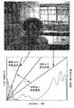
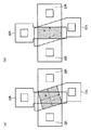
図14および図15は、従来の半導体撮像素子による撮像例を示す第1および第2の図である。
【0006】
図14および図15を参照して、これらの撮像例は、晴れた昼間に蛍光灯を点灯した室内から窓外を含む光景を撮影したものである。このような光景は、日常生活において、よく目にする、ありふれた状景である。このような普段の光景において、ヒトの目では、室内も窓外の光景も難無く十分なコントラストで見えることは、経験上、明白である。
【0007】
しかしながら、従来の半導体撮像素子では、図14の撮像例のように、室内を見えるように画素の受光感度特性を調整すると、窓の外が明るくなり過ぎて、明るい部分のコントラストを検知することができなくなる。一方、図15の撮像例のように、窓外の光景を十分なコントラストで見えるように調整すると、今度は室内が暗くなり過ぎて、暗い部分のコントラストを検知することが困難となる。このように、従来のイメージセンサーでは、視野内に明るい領域と暗い領域とが同時に混在する場合には、全領域で十分なコントラストを検知する能力が、ヒトの視覚検知と比べて大きく劣っていることが分かる。
【0008】
したがって、従来の半導体撮像素子をヒトの視覚に代わる視覚情報検知装置として用いるためには、このコントラスト感知能力の低さが、実用化する上で解決しなければならない、大きな課題の一つである。
【0009】
次に、図16を用いて従来の半導体撮像素子のコントラスト検知能力の低さを説明する。
【0010】
一般的に、晴れた昼間の屋外の照度は、数万ルクス程度である。一方、蛍光灯を点灯した室内の照度は、太陽光が射し込まない所で約500ルクス程度で、暗い所では100ルクス以下になる。つまり、図14および15に示した撮像例では、図16内の輝度分布例で示すように、窓外の輝度分布と、室内の暗い部分(顔部分)の輝度分布は、各々の平均値で2〜3桁も差があることになる。
【0011】
図14の撮像例では、室内の比較的明るい領域(500ルクス以下)において十分なコントラストを感知できるように、画素の受光感度特性が図16に示す感度直線になるように調整されている。しかし、既に述べたように、従来の半導体撮像素子では全ての画素が同じ感度特性を有しているので、このような受光感度特性で撮像すると、窓外の明るい部分は受光感度が飽和してしまい真っ白となる。一方、暗い部分においても、全体の1/5以下の振幅となり十分なコントラストを得ることができないことが分かる。このように、従来の半導体撮像素子では、我々が日常で多く遭遇する状景にすら、十分なコントラストを感知することができないことになる。
【0012】
この発明は、このような問題点を解決するためになされたものであって、この発明の目的は、一視野内の輝度分布が大きい場合であっても、明るい部分と暗い部分とを十分なコントラストで検知可能な半導体撮像素子を提供することである。
【0013】
【課題を解決するための手段】
この発明に従う半導体撮像素子は、イメージセンサーを構成する画素回路において、画素毎に固有の信号増幅率を調整できる機能を備えたことを特徴とする。
【0014】
好ましくは、画素回路は、画素固有の検知受光信号の読み出し増幅率を、周辺画素を含む近傍検知受光信号の平均信号で変調することを特徴とする。
【0015】
さらに好ましくは、画素回路は、利得係数βを電気的にアナログ変調できるMOSトランジスタを信号読出し増幅に用いることを特徴とする。
【0016】
特にこのような構成においては、画素回路において、MOSトランジスタの利得係数βを変調するためのβ制御ゲートには、周辺の平均受光量信号が入力される。
【0017】
あるいは好ましくは、周辺の平均受光量信号は、ウェルと基板間で形成されるダイオードと、ウェルの形状で設定される画素間の接続抵抗によって与えられることを特徴とする。
【0018】
さらに好ましくは、各画素の受光信号を与えるフォトダイオードを、ウェル内に形成することを特徴とする。
【0019】
この発明の他の構成に従う半導体撮像素子は、複数の画素を備える。各画素は、自身および自身の周辺に配置された他の複数の画素のうちの少なくとも一部の画素における光量に応じて調整される信号増幅率に従って、自身における入射光量に応じた電気信号を生成する画像信号生成回路を含む。
【0020】
好ましくは、信号増幅率は、少なくとも一部の画素における平均光量に応じて設定される。
【0021】
また好ましくは、複数の画素のそれぞれにおける信号増幅率は、少なくとも一部の画素における平均光量が小さい領域において、平均光量が大きい領域よりも相対的に大きく設定される。
【0022】
あるいは好ましくは、各画素は、自身への入射光量に応じた第1の電位を第1のノードに生成するための第1の受光検知素子と、少なくとも一部の画素への入射光量に応じた第2の電位を第2のノードに生成するための第2の受光検知素子とをさらに含む。画像信号生成回路は、第1および第2の電位の積に応じて電気信号を生成する。
【0023】
さらに好ましくは、第1の電位は、自身への入射光量の増加に応じて上昇し、第2の電位は、少なくとも一部の画素への入射光量の増加に応じて下降する。
【0024】
あるいは、さらに好ましくは、第1の電位は、自身への入射光量の増加に応じて下降し、第2の電位は、少なくとも一部の画素への入射光量の増加に応じて上昇する。
【0025】
また、さらに好ましくは、第1の受光検知素子は、第1のノードから第1の固定電圧へ向かう方向を順方向として、第1の固定電圧および第1のノードの間に接続された第1のダイオードを有し、第2の受光検知素子は、第2の固定電圧から第2のノードへ向かう方向を順方向として、第2のノードおよび第2の固定電圧の間に接続された第2のダイオードを有する。少なくとも一部の画素において、第2のノード同士は抵抗成分を介して電気的に結合される。
【0026】
また、さらに好ましくは、第1の受光検知素子は、第1の固定電圧から第1のノードへ向かう方向を順方向として、第1の固定電圧および第1のノードの間に接続された第1のダイオードを有し、第2の受光検知素子は、第2のノードから第2の固定電圧へ向かう方向を順方向として、第2のノードおよび第2の固定電圧の間に接続された第2のダイオードを有する。少なくとも一部の画素において、第2のノード同士は抵抗成分を介して電気的に結合される。
【0027】
あるいは好ましくは、画像信号生成回路は、制御ゲートへの印加電圧に応じて利得係数をアナログ変調可能な電界効果型トランジスタを含む。電界効果型トランジスタの制御ノードは、第2のノードと接続され、電界効果型トランジスタは、利得係数に従って第1のノードの電位を増幅することによって電気信号を生成する。
【0028】
また好ましくは、半導体撮像素子は、第1導電型の基板上に生成され、基板上に形成された、第1導電型とは反対導電型の第2導電型のウェル領域をさらに備える。第2の受光検知素子は、基板およびウェル領域の間の接合を用いて形成されるダイオードを有する。
【0029】
さらに好ましくは、第2のノードは、ウェル領域に相当する。
あるいは、さらに好ましくは、半導体撮像素子は、ウェル領域内に形成された第1導電型の第1拡散領域と、第1拡散領域内に形成された第2導電型の第2拡散領域とをさらに備える。第1および第2拡散領域は、各画素ごとに独立に設けられ、第1の受光検知素子は、第1拡散領域および第2拡散領域の間の接合を用いて形成されるダイオードを有する。
【0030】
また好ましくは、半導体撮像素子は、第1および第2のノードの電位を所定周期で所定電位にそれぞれリセットするためのリセット回路をさらに備える。
【0031】
あるいは好ましくは、半導体撮像素子は、所定周期で第1のノードの電位を所定電位にリセットするとともに、第2のノードを固定のバイアス電圧と抵抗成分を介して電気的に結合するためのリセット回路をさらに備える。
【0032】
【発明の実施の形態】
以下において、本発明の実施の形態を図面を参照して詳細に説明する。なお、以下の説明において、同一または相当部分については同一の参照符号を付すものとする。
【0033】
[実施の形態1]
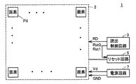
図1は、本発明の実施の形態に従う半導体撮像素子の構成を示す概略ブロック図である。
【0034】
図1を参照して、本発明に従う半導体撮像素子1は、複数の画素PXが行列状に配置された画素アレイ2と、読出制御回路3と、リセット回路5と、電源回路7とを備える。
【0035】
読出制御回路3は、画素アレイ2における画像データ生成タイミングを制御するための制御信号RDを生成する。リセット回路5は、各画素PXにおける受光検知素子の状態を定期的にリセットする。リセット回路5によるリセット動作タイミングは、読出制御回路3からのリセット信号Rst0,Rst1によって制御される。電源回路7は、画素アレイ2内の各画素に対して、電源電圧Vdおよび接地電圧GNDを供給する。
【0036】
図2は、各画素の構成を説明するブロック図である。図2においては、行列状に配置された複数の画素のうちの、第i行・第j列(i,j:自然数)の画素PX(i,j)および、これに隣接する画素群が代表的に示される。
【0037】
図2を参照して、各画素PXは、受光検知素子であるフォトダイオードPD0,PD1と、画素信号生成回路10と、画素データ生成回路15とを含む。
【0038】
フォトダイオードPD1は、当該画素における入射光量に応じた電位を有する信号を生成する。フォトダイオードPD0は、周辺領域の複数の画素中のフォトダイオードPD0と、抵抗成分を介して電気的に結合される。これにより、各画素のフォトダイオードPD0は、当該画素の周辺領域における平均光量に対応する電位を有する信号を生成することができる。
【0039】
図2の構成例においては、各画素は、隣接する4個の画素との間でフォトダイオードPD0同士が電気的に結合されている。たとえば、画素PX(i,j)は、画素PX(i,j+1)、PX(i,j−1)、PX(i−1,j)およびPX(i+1,j)との間で電気的に結合される。しかし、本願発明の適用は、このような構成に限定されず、各画素のフォトダイオードPD0は、周囲に配置された任意の個数の他の画素のフォトダイオードPD0と接続する構成とすることができる。
【0040】
画素信号生成回路10は、フォトダイオードPD0およびPD1のそれぞれの出力に応じて、制御信号RDに応答したタイミングで、当該画素での入射光量に応じた画像信号を出力信号として生成する。画像信号は、フォトダイオードPD0の出力、すなわち当該画素の周辺領域における平均光量に基づいて自動調整された受光感度特性(信号増幅率)に従って、フォトダイオードPD1の出力、すなわち当該画素での光量に応じた強度を有する。
【0041】
したがって、各画素の受光感度特性は、当該画素の周辺領域における平均光量に基づいて自動調整されることになる。具体的には、各画素において、周辺の平均光量に反比例して、その画素の受光感度(信号増幅率)を大きくするように設定すればよい。すなわち、各画素は、暗い領域においては受光感度を相対的に大きく設定し、明るい領域においては受光感度を相対的に小さく設定するような自動調整機能を有する。
【0042】
画素データ生成回路15は、画素信号生成回路10からの出力信号(画素信号)をアナログ/デジタル変換して画像データDATを生成し、かつ生成された画像データを一時的に保持する。画像データ生成回路15に保持された画像データDATは、図示しない走査回路を用いて、画素単位、画素の行単位あるいは列単位、もしくは画素アレイ一括で、任意の範囲ごとに半導体撮像素子外部から読出すことができる。なお、図示しない各画素においても、その内部構成および、周囲の画素との間における接続関係は、同様である。
【0043】
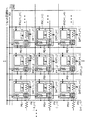
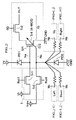
図3は、各画素の構成を詳細に示す回路図である。
図3を参照して、画素への入射光量に応じた電位Vaを与えるフォトダイオードPD1と、周辺の平均光量に応じた電位Vbを与えるフォトダイオードPD0とを有し、それぞれのフォトダイオードによって与えられた電位VaおよびVbの積算結果を画素信号として読み出す回路構成となっている。
【0044】
フォトダイオードPD1は、ノードNaから電源電圧Vdへ向かう方向を順方向として、ノードNaおよび電源電圧Vdの間に接続される。フォトダイオードPD0は、接地電圧GNDからノードNbへ向かう方向を順方向として、ノードNbおよび接地電圧GNDの間に接続される。
【0045】
リセット回路5は、ノードNaとリセット電圧Vtとの間に接続されたリセット用トランジスタTr1と、ノードNbとリセット電圧Vdmとの間に接続されたリセット用トランジスタTr0とを有する。リセット用トランジスタTr0おょびTr1は、リセット信号Rst0およびRst1にそれぞれ応答してターンオンする。
【0046】
リセット電圧Vtは、リセット時に、フォトダイオードPD1に所定の逆バイアス電圧を印加するための電圧であり、接地電圧GNDを用いることもできる。同様に、リセット電圧Vdmは、リセット時に、フォトダイオードPD0に所定の逆バイアス電圧を印加するための電圧であり、電源電圧Vdを用いることもできる。これらのバイアス電圧については、たとえば図1に示した電源回路7から供給する構成とすることができる。
【0047】
したがって、リセット回路5によるリセット動作によって、ノードNaおよNbは、所定電圧(Vt,Vdm)と接続される。その後、フォトダイオードPD1には、当該画素での光量に応じた逆方向電流が生じるので、電位Vaは、当該画素の受光量に応じて時間的に変化する。
【0048】
図2で説明したように、各画素中のノードNbは、他の画素中のノードNbと抵抗成分を介して電気的に結合される。たとえば、図3の構成においては、たとえば、画素PX(i,j)中のノードNbは、上側(up)の画素PX(i−1,j)、下側(down)の画素PX(i+1,j)、左側(1eft)の画素PX(i,j−1)および右側(right)の画素PX(i,j+1)のそれぞれの内部のノードNbと、抵抗成分を介して電気的に結合されている。
【0049】
したがって、ノードNbの電位は、当該画素内のフォトダイオードPD0に生じる逆方向電流のみならず、電気的に結合された他の画素内のフォトダイオードPD0に生じる逆方向電流の影響を受けて時間的に変化する。このように、周辺の画素内のフォトダイオードPD0同士を抵抗成分を介して接続することによって、当該画素の周辺光量に反比例した電位VbをノードNbに生成できる。
【0050】
画素信号生成回路10は、積算器PUと読出選択スイッチトランジスタTr2とを有する。積算器PUは、ノードNaおよびNbのそれぞれの電位VaおよびVbの積に相関する電流iを、ノードNcおよび接地電圧GNDの間に生成する。すなわち、積算器PUの電流特性式はi=f(Va×Vb)で示され、電流iは、電位VaおよびVbの積にほぼ比例する。
【0051】
読出選択スイッチトランジスタTr2は、制御信号RDの活性化タイミングにおけるノードNcの電位を画像信号OUTとして出力する。
【0052】
このような構成とすることにより、ノードNaの電位Vaが同レベルであっても、周辺の平均光量が少ない画素、つまり暗い部分の画素においては、ノードNcの電位は、相対的に高くなり、周辺の平均光量が多い画素、つまり明るい部分の画素では、ノードNcの電位は、相対的に低くなる。したがって、各画素の受光感度を、暗い領域においては大きくし明るい領域では小さくする、画素毎の信号増幅率制御を実現している。
【0053】
図4は、本発明に従う半導体撮像素子の画素特性を示す概念図およびその撮像例を示す図である。
【0054】
図4を参照して、本発明に従う半導体撮像素子においては、受光感度特性を各画素毎に自動調整する機能を備えることによって、各画素毎に、周辺の平均光量に反比例してその画素における感度直線(信号増幅率)を変化させるような(暗い所程増幅率を大きくする)、自動調整機能が実現される。さらに、このような機能を搭載した半導体撮像素子において、視野内の最も明るい部分で十分なコントラストが維持できるように全画素共通の蓄積時間(露光時間)を調整すれば、暗い部分の信号がその周辺の暗さに応じて増幅されるので、暗い部分のコントラストが増強され、画面の全領域で十分なコントラストが検知できるようになる。露光時間は、リセット信号Rst0,Rst1に応答してリセット動作が実行されてから、制御信号RDが活性化されるまでの期間に相当し、読出制御回路3によって設定される。この結果、図4に示される撮像例のように、明るい部分も暗い部分も十分なコントラストで検知できる半導体撮像素子を実現することができる。
【0055】
[実施の形態2]
実施の形態2においては、このような信号増幅率制御に適した、積算器PUの構成について説明する。実施の形態2においては、制御ゲートへの入力電圧に応じて利得係数βを制御することが可能なMOSトランジスタ(以下、「A−MOS(Adjustable β-MOS)デバイス」とも称する)を用いて、画素毎に受光感度特性を自動調整する機能を実現する。
【0056】
図5は、A−MOSデバイスの素子構成例を示す概念図である。
図5を参照して、A−MOSデバイスは、通常のMOSトランジスタと同様の通常ゲートGR、ソースSRおよびドレインDRに加えて、通常ゲートと一定角度を持つように形成される制御ゲートCGをさらに有する。
【0057】
図6は、A−MOSデバイスの素子構成パラメータを示す概念図である。
図6を参照して、A−MOSデバイスは、通常ゲートGRのゲート長Lr、ゲート幅Wrおよび、通常ゲートGRと制御ゲートCGとの成す角度θを素子構成パラメータとして有する。
【0058】
図7は、A−MOSデバイスにおけるβ変調の原理を説明する概念図である。図7(a)を参照して、制御ゲートCG下チヤネルのコンダクタンスが通常ゲートと同等となるように、制御ゲートCGの印加電圧を設定した場合には、図中にハッチングで示した部分が実効的なゲート領域となる。すなわち、実効的なゲート長Lは、通常ゲートGRのゲート長Lrよりも長くなり、実効的なゲート幅Wは、通常ゲートGRのゲート幅Wrよりも狭くなるので、利得係数βは低下する。
【0059】
一方、図7(b)を参照して、制御ゲートCG下のチヤネルのコンダクタンスが通常ゲートよりも十分に大きくなるように、制御ゲートCGの印加電圧を設定した場合には、実効的なゲート幅Wおよびゲート長Lは、通常ゲートGRのゲート幅Wrおよびゲート長Lrと同等となる。
【0060】
このように、A−MOSデバイスは、制御ゲートCGの印加電圧を変えることで、実効的なゲート長Lおよびゲート幅Wをアナログ的に変調することができる。その結果、A−MOSデバイスは、制御ゲート電圧による利得係数βのアナログ変調を実現している。このようにA−MOSデバイスは、10〜1000倍程度のβ変調特性を、比較的コンパクトに実現できる特長を有している。A−MOSデバイスにおける利得係数βの変調特性は、図6に示したパラメータによって設定することができる。
【0061】
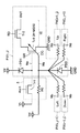
図8は、実施の形態2に従う各画素の構成を示す回路図である。
図8を参照して、実施の形態2に従う構成においては、積算器PUに代えて、ノードNcおよび接地電圧GNDの間に電気的に結合されるA−MOSトランジスタTr4が設けられる。A−MOSトランジスタTr4の通常ゲートGRは、ノードNaと接続され、制御ゲートCGは、ノードNbと接続される。
【0062】
このように、実施の形態2においては、画素への入射光量に応じて電位が変わるフォトダイオードPD1がA−MOSトランジスタTr4の通常ゲートに接続され、周辺の平均光量に応じた電位ノードNbがA−MOSトランジスタTr4の制御ゲートに接続された構成になっている。すでに説明したように、周辺の平均光量に応じた電位は、周辺の画素と抵抗成分を介して接続された平均光量検出用のフォトダイオードPD0によって与えられる。
【0063】
この構成によって、周辺の平均光量が少ない画素、つまり暗い部分の画素では、A−MOSトランジスタの利得係数βを大きくし、明るい部分の画素ではβを小さくする画素毎の制御を実現している。言い換えれば、A−MOSトランジスタによって、図3に示した積算器PUの機能を実現することができる。
【0064】
このような画素毎のβ調整によって、実施の形態1と同様に、暗い部分の画素における信号増幅率は明るい部分の画素よりも大きくなる。その結果、暗い所のコントラストを高めることが可能となる。リセット回路5および、各画素のその他の部分の構成は、実施の形態1と同様であるので、詳細な説明は繰り返さない。
【0065】
このように、A−MOSデバイスを各画素の信号読み出し増幅トランジスタとして用いれば、A−MOSデバイスの制御ゲートに周辺平均光量を示す電圧を与えるだけの比較的簡単な回路構成で、周辺が暗い時にその画素の増幅率を100倍程度まで高める自動調整機能を実現できると共に、この画素毎の自動調整機能を搭載することで生じる画素面積の増大を抑えることができる。
【0066】
[実施の形態3]
実施の形態3においては、各画素に設けられる2個のフォトダイオードの効率的な配置について説明する。
【0067】
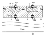
図9は、実施の形態3に従うフォトダイオードの配置例を示す構造図である。図9を参照して、半導体撮像素子が形成されるP型シリコン基板(P−sub)20と、P型シリコン基板20上に設けられたNウェル21との間に形成されるPN接合を用いて、周辺領域の平均光量を検知するためのフォトダイオードPD0が構成される。
【0068】
さらに、当該Nウェル21内に形成されたP+領域22と、P+領域22内に形成されたN+領域23との間で形成されるPN接合を用いて、当該画素への入射光量を検知するためのフォトダイオードPD1が構成される。なお、P+領域22およびN+領域23の不純物濃度は、P型シリコン基板20およびNウェル21よりも比較的高い。
【0069】
P+領域22およびN+領域23は、画素ごとに独立に設けられる。また、同一のNウェル21内に作製された複数の画素間は、Nウェルの拡散抵抗を介して電気的に結合される。すなわち、各画素におけるNウェル21は、図3の回路構成におけるノードNbに相当する。したがって、同一のNウェル21に作製された複数の画素間でノードNbが電気的に結合されて、平均光量が検知される。
【0070】
あるいは、画素アレイ2全体を同一のNウェル上に形成してもよい。この場合には、各画素において、当該画素のフォトダイオードPD0と、他の画素のフォトダイオードPD0との間の電気抵抗値は、画素間の距離に対応して増大する。したがって、各画素におけるノードNbの電位Vbは、近接する画素への入射光量の影響を相対的に大きく受けるので、結果的には電位Vbによって画素周辺領域の平均光量を検知することができる。
【0071】
実施の形態3に従うフォトダイオードの配置によれば、各画素に設けられる2個のフォトダイオードが縦構造で配置されている。さらに、周辺の画素間におけるフォトダイオード間の抵抗接続を、特別な配線等を設けることなくNウェルの形状で構成できる。したがって、各画素および画素アレイの面積の増大を防ぐことができる。
【0072】
[実施の形態4]
図10は、実施の形態4に従う画素の構成を示す回路図である。
【0073】
図10を図8と比較して、実施の形態4に従う構成においては、フォトダイオードPD0に対応して設けられるリセット用トランジスタTr0に代えて、抵抗器R0が、リセット電圧(たとえば電源電圧Vd)とノードNbとの間に接続される。その他の部分の構成は、図8と同様であるので、詳細な説明は繰り返さない。
【0074】
このような構成としても、ノードNbは、当該画素および当該画素と電気的に結合された周辺画素内のフォトダイオードPD0への入射光量に応じた電位に落ち着くので、実施の形態1または2における構成と同様に、ノードNbの電位Vbによって画素周辺領域の平均光量を検知できる。したがって、周辺平均光量の検知動作について定期的なリセット操作を必要としないので、リセット回路5の構成を簡略化できる。なお、同様の構成は、実施の形態1に従う図3に示した回路構成に対しても適用できる。
【0075】
[実施の形態5]
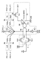
図11は、実施の形態5に従う画素の構成を示す回路図である。
【0076】
図11を図8と比較して、実施の形態5に従う構成においては、実施の形態2に従う構成から、フォトダイオードの配置が入換えられている。すなわち、フォトダイオードPD0は、ノードNbから電源電圧Vdへ向かう方向を順方向として、ノードNbおよび電源電圧Vdの間に接続され、フォトダイオードPD1は、接地電圧GNDからノードNaへ向かう方向を順方向として、接地電圧GNDおよびノードNaの間に接続される。これに対応して、読出選択スイッチトランジスタTr2およびA−MOSトランジスタTr4は、Nチヤネル型からPチヤネル型に変更される。なお、同様の構成は、実施の形態1に従う図3に示した回路構成に対しても適用できる。
【0077】
図12は、実施の形態5に従うフォトダイオードの配置例を示す構造図である。
【0078】
図12を参照して、実施の形態5においては、半導体撮像素子が形成されるN型シリコン基板(N−Sub)30上に設けられたPウェル31との間に形成されるPN接合を用いて、画素周辺領域の平均光量を検知するためのフォトダイオードPD0が構成される。さらに、当該Pウェル31内に形成されたN+領域32と、N+領域32内に形成されたP+領域33との問で形成されるPN接合を用いて、当該画素への入射光量を検知するためのフォトダイオードPD1が構成される。
【0079】
図9に示した構造と同様に、N+領域32およびP+領域33は、画素ごとに独立に設けられ、N+領域32およびP+領域33の不純物濃度は、N型シリコン基板30およびPウェル31よりも比較的高い。また、Pウェル31の設計については、図9におけるNウェル21と同様にすればよい。
【0080】
このように、フォトダイオードの配置を入換えた構成としても、実施の形態1または2と同様に、各画素毎において周辺平均光量に応じて感度直線(増幅率)を変化させるような自動調整機能を実現して、画面の全領域で十分なコントラストが検知できるようになる。さらに、実施の形態3と同様に、各画素ごとに2個のフォトダイオードを必要とする構成においても、各画素および画素アレイの面積の増大を防ぐことができる。
【0081】
[実施の形態6]
図13は、実施の形態6に従う画素の構成を示す回路図である。
【0082】
図13を図11と比較して、実施の形態6に従う構成においては、フォトダイオードPD0に対応して設けられるリセット用トランジスタTr0に代えて、抵抗器R0が、リセット電圧である接地電圧GNDとノードNbとの間に接続される。その他の部分の構成は、図11と同様であるので、詳細な説明は繰り返さない。
【0083】
このように、フォトダイオードの配置を入換えた構成においても、実施の形態4と同様に、リセット回路5の構成を簡略化した上で、画面の全領域で十分なコントラストが検知できるようになる。また、図13に従う回路構成においても、各画素に必要な2個のフォトダイオードPD0,PD1は、図12の構造図と同様に、各画素および画素アレイの面積の増大を防止して配置できる。
【0084】
今回開示された実施の形態はすべての点で例示であって制限的なものではないと考えられるべきである。本発明の範囲は上記した説明ではなくて特許請求の範囲によって示され、特許請求の範囲と均等の意味および範囲内でのすべての変更が含まれることが意図される。
【0085】
【発明の効果】
以上説明したように、この発明によれば、一般にCMOSイメージセンサーはS/N比が60〜65dB程度なので、画面の中で最も暗い所の画質を20dB程度まで許せば、本発明の半導体撮像素子(イメージセンサー)は、数百倍程度の平均輝度差まで、十分なコントラストを全画面で検知できると見積られる。
【0086】
また、本発明の半導体撮像素子(イメージセンサー)は、受光感度特性を画素毎にアナログ調整できる機能を、コンパクトに実装できるので、従来のイメージセンサーと比べて感度および解像度で劣ることがない。
【0087】
さらに、本発明の半導体撮像素子(イメージセンサー)は、従来のイメージセンサーでは検知することが困難だった、同一視野内の大きな輝度差の画像を、十分なコントラストで検知することができ、ヒトの知覚能力に近い優れた撮像装置として利用することができる。従って、このイメージセンサーは、監視装置や車載用カメラ等の、急激な環境変化への対応が要求される分野で威力を発揮できる。
【図面の簡単な説明】
【図1】 本発明の実施の形態に従う半導体撮像素子の構成を示す概略ブロック図である。
【図2】 各画素の構成を説明するブロック図である。
【図3】 各画素の構成を詳細に示す回路図である。
【図4】 本発明に従う半導体撮像素子の画素特性を示す概念図およびその撮像例を示す図である。
【図5】 A−MOSデバイスの素子構成例を示す概念図である。
【図6】 A−MOSデバイスの素子構成パラメータを示す概念図である。
【図7】 A−MOSデバイスにおけるβ変調の原理を説明する概念図である。
【図8】 実施の形態2に従う各画素の構成を示す回路図である。
【図9】 実施の形態3に従うフォトダイオードの配置例を示す構造図である。
【図10】 実施の形態4に従う画素の構成を示す回路図である。
【図11】 実施の形態5に従う画素の構成を示す回路図である。
【図12】 実施の形態5に従うフォトダイオードの配置例を示す構造図である。
【図13】 実施の形態6に従う画素の構成を示す回路図である。
【図14】 従来の半導体撮像素子による撮像例を示す第1の図である(室内可視)。
【図15】 従来の半導体撮像素子による撮像例を示す第2の図である(室外可視)。
【図16】 従来の半導体撮像素子のコントラスト検知能力の低さを説明する図である。
【符号の説明】
1 半導体撮像素子
2 画素アレイ
3 読出制御回路
5 リセット回路
7 電源回路
10 画素信号生成回路
15 画素データ生成回路
20 P型シリコン基板
21 Nウェル
22,33 P+領域(不純物濃度が比較的高い)
23,32 N+領域(不純物濃度が比較的高い)
30 N型シリコン基板
CG 制御ゲート
GND 接地電圧
GR 通常ゲート
L 実効ゲート長(A−MOSトランジスタ)
Na,Nb,Nc ノード
OUT 画像信号
PD0 フォトダイオード(周辺画素平均受光検知用)
PDI フォトダイオード(当該画素内受光検知用)
PU 積算器
PX 画素
R0 抵抗器
Rst0,Rst1 リセット信号
Tr0,Tr1 リセット用トランジスタ
Tr2 読出選択スイッチトランジスタ
Tr4 A−MOSトランジスタ(Adjustable−MOSトランジスタ)
Vd 電源電圧
Vdm,Vt リセット電圧
W 実効ゲート幅(A−MOSトランジスタ)
β 利得係数[0001]
BACKGROUND OF THE INVENTION
The present invention relates to a semiconductor imaging device that realizes a light receiving sensing characteristic close to human visual sensing characteristics. More specifically, even if a region with a large luminance difference is mixed in a visual field, sufficient contrast is detected in the entire region. The present invention relates to a semiconductor imaging device capable of performing the same. Therefore, the technology of the present invention can be used for a surveillance camera including the outdoors, a vehicle-mounted camera, and the like that are used in various situations as an imaging apparatus having a high visual sensing capability.
[0002]
[Prior art]
Solid-state imaging devices such as CCD (Charge-coupled device) and CMOS (complementary mental-oxide semiconductor) imagers, so-called semiconductor image sensors (hereinafter also referred to as “semiconductor imaging devices”) are used in video cameras and digital cameras. Now, it is also incorporated in mobile phones and the like, and it is widely used as an image sensor with low cost and low power consumption.
[0003]
However, the sensing ability of the semiconductor image sensor is greatly inferior to human visual sensing. In human vision, even if there is a luminance distribution of about 4 to 5 digits in one visual field, it is possible to sufficiently detect the contrast between a bright place and a dark place. This excellent contrast sensing ability is realized by a function that allows the light-receiving cells in the retina to adjust their light-sensitive characteristics for each individual cell.
[0004]
On the other hand, in the conventional semiconductor image sensor, since all the pixels have the same light receiving characteristics, it is difficult to obtain sufficient contrast simultaneously in a bright place and a dark place in the field of view.
[0005]
[Problems to be solved by the invention]
14 and 15 are first and second diagrams showing an example of imaging by a conventional semiconductor imaging device.
[0006]
With reference to FIGS. 14 and 15, these imaging examples are taken of a scene including the outside of a window from a room in which a fluorescent lamp is lit during a clear daytime. Such a scene is a common scene that is often seen in daily life. In such a normal scene, it is clear from experience that the human eye can see the room and the scene outside the window with sufficient contrast without difficulty.
[0007]
However, in the conventional semiconductor imaging device, as shown in the imaging example of FIG. 14, when the light receiving sensitivity characteristic of the pixel is adjusted so that the room can be seen, the outside of the window becomes too bright and the contrast of the bright part can be detected. become unable. On the other hand, if the scene outside the window is adjusted so that it can be seen with sufficient contrast as in the imaging example of FIG. 15, the room becomes too dark this time, and it becomes difficult to detect the contrast of the dark part. As described above, in the conventional image sensor, when a bright region and a dark region are mixed at the same time in the field of view, the ability to detect sufficient contrast in the entire region is greatly inferior to human visual detection. I understand that.
[0008]
Therefore, in order to use a conventional semiconductor imaging device as a visual information detection device that replaces human vision, this low contrast sensing capability is one of the major issues that must be solved before practical use. .
[0009]
Next, the low contrast detection capability of a conventional semiconductor image sensor will be described with reference to FIG.
[0010]
Generally, the illuminance outdoors on a sunny day is about tens of thousands of lux. On the other hand, the illuminance in the room where the fluorescent lamp is turned on is about 500 lux in places where sunlight does not enter, and is 100 lux or less in dark places. That is, in the imaging examples shown in FIGS. 14 and 15, as shown in the luminance distribution example in FIG. 16, the luminance distribution outside the window and the luminance distribution of the dark part (face part) in the room are average values. There will be a difference of 2 to 3 digits.
[0011]
In the imaging example of FIG. 14, the light reception sensitivity characteristic of the pixel is adjusted to be a sensitivity straight line shown in FIG. 16 so that sufficient contrast can be sensed in a relatively bright area (500 lux or less) in the room. However, as already mentioned, all pixels in the conventional semiconductor image sensor have the same sensitivity characteristics, so when imaging with such light reception sensitivity characteristics, the light reception sensitivity is saturated in bright areas outside the window. It turns white. On the other hand, even in a dark part, it can be seen that the amplitude is 1/5 or less of the whole and sufficient contrast cannot be obtained. As described above, the conventional semiconductor imaging device cannot sense a sufficient contrast even in a scene that we often encounter on a daily basis.
[0012]
The present invention has been made to solve such a problem, and the object of the present invention is to sufficiently provide a bright portion and a dark portion even when the luminance distribution in one field of view is large. It is an object of the present invention to provide a semiconductor imaging device capable of detecting with contrast.
[0013]
[Means for Solving the Problems]
The semiconductor image pickup device according to the present invention is characterized in that a pixel circuit constituting the image sensor has a function of adjusting a specific signal amplification factor for each pixel.
[0014]
Preferably, the pixel circuit modulates the read amplification factor of the detection light reception signal unique to the pixel with an average signal of the proximity detection light reception signals including the peripheral pixels.
[0015]
More preferably, the pixel circuit uses a MOS transistor capable of electrically analog-modulating the gain coefficient β for signal readout amplification.
[0016]
Particularly in such a configuration, a peripheral average received light amount signal is input to the β control gate for modulating the gain coefficient β of the MOS transistor in the pixel circuit.
[0017]
Alternatively, preferably, the peripheral average received light amount signal is given by a diode formed between the well and the substrate and a connection resistance between the pixels set in the shape of the well.
[0018]
More preferably, a photodiode for providing a light reception signal of each pixel is formed in the well.
[0019]
A semiconductor imaging device according to another configuration of the present invention includes a plurality of pixels. Each pixel generates an electrical signal corresponding to the amount of incident light in accordance with the signal amplification factor adjusted according to the amount of light in at least some of the other pixels arranged in itself and in the periphery of the pixel. Including an image signal generation circuit.
[0020]
Preferably, the signal amplification factor is set according to an average light amount in at least some of the pixels.
[0021]
Preferably, the signal amplification factor in each of the plurality of pixels is set to be relatively larger in a region where the average light amount is small in at least some of the pixels than in a region where the average light amount is large.
[0022]
Alternatively, preferably, each pixel corresponds to the first light receiving detection element for generating a first potential corresponding to the amount of incident light on the first node and the amount of incident light to at least some of the pixels. And a second light receiving detection element for generating a second potential at the second node. The image signal generation circuit generates an electrical signal according to the product of the first and second potentials.
[0023]
More preferably, the first potential increases with an increase in the amount of incident light on itself, and the second potential decreases with an increase in the amount of incident light on at least some of the pixels.
[0024]
Alternatively, more preferably, the first potential decreases with an increase in the amount of incident light on itself, and the second potential increases with an increase in the amount of incident light on at least some of the pixels.
[0025]
More preferably, the first light receiving detection element is connected between the first fixed voltage and the first node with the direction from the first node toward the first fixed voltage as a forward direction. The second light-receiving detection element is connected between the second node and the second fixed voltage with the direction from the second fixed voltage to the second node as the forward direction. Of diodes. In at least some of the pixels, the second nodes are electrically coupled to each other through a resistance component.
[0026]
More preferably, the first light receiving detection element is connected between the first fixed voltage and the first node with a direction from the first fixed voltage toward the first node as a forward direction. The second light receiving detection element is connected between the second node and the second fixed voltage with the direction from the second node toward the second fixed voltage as a forward direction. Of diodes. In at least some of the pixels, the second nodes are electrically coupled to each other through a resistance component.
[0027]
Alternatively, preferably, the image signal generation circuit includes a field effect transistor capable of analog-modulating a gain coefficient in accordance with a voltage applied to the control gate. The control node of the field effect transistor is connected to the second node, and the field effect transistor generates an electric signal by amplifying the potential of the first node according to the gain coefficient.
[0028]
Preferably, the semiconductor imaging device further includes a well region of a second conductivity type generated on the substrate of the first conductivity type and formed on the substrate and having a conductivity type opposite to the first conductivity type. The second light receiving detection element has a diode formed using a junction between the substrate and the well region.
[0029]
More preferably, the second node corresponds to a well region.
Alternatively, more preferably, the semiconductor imaging device further includes a first conductivity type first diffusion region formed in the well region and a second conductivity type second diffusion region formed in the first diffusion region. Prepare. The first and second diffusion regions are provided independently for each pixel, and the first light receiving detection element has a diode formed using a junction between the first diffusion region and the second diffusion region.
[0030]
Preferably, the semiconductor imaging device further includes a reset circuit for resetting the potentials of the first and second nodes to a predetermined potential at a predetermined cycle.
[0031]
Alternatively, preferably, the semiconductor imaging device resets the potential of the first node to a predetermined potential in a predetermined cycle, and electrically couples the second node via a fixed bias voltage and a resistance component. Is further provided.
[0032]
DETAILED DESCRIPTION OF THE INVENTION
Hereinafter, embodiments of the present invention will be described in detail with reference to the drawings. In the following description, the same or corresponding parts are denoted by the same reference numerals.
[0033]
[Embodiment 1]
FIG. 1 is a schematic block diagram showing a configuration of a semiconductor imaging device according to an embodiment of the present invention.
[0034]
Referring to FIG. 1, a
[0035]
The read control circuit 3 generates a control signal RD for controlling the image data generation timing in the
[0036]
FIG. 2 is a block diagram illustrating the configuration of each pixel. In FIG. 2, the pixel PX (i, j) in the i-th row and j-th column (i, j: natural number) and the pixel group adjacent thereto are representative among the plurality of pixels arranged in a matrix. Indicated.
[0037]
Referring to FIG. 2, each pixel PX includes photodiodes PD <b> 0 and PD <b> 1 that are light receiving detection elements, a pixel
[0038]
The photodiode PD1 generates a signal having a potential corresponding to the amount of incident light in the pixel. Photodiode PD0 is electrically coupled to photodiode PD0 in a plurality of pixels in the peripheral region via a resistance component. Thereby, the photodiode PD0 of each pixel can generate a signal having a potential corresponding to the average light amount in the peripheral region of the pixel.
[0039]
In the configuration example of FIG. 2, in each pixel, the photodiodes PD0 are electrically coupled to four adjacent pixels. For example, the pixel PX (i, j) is electrically connected to the pixel PX (i, j + 1), PX (i, j-1), PX (i-1, j), and PX (i + 1, j). Combined. However, the application of the present invention is not limited to such a configuration, and the photodiode PD0 of each pixel can be connected to the photodiode PD0 of an arbitrary number of other pixels arranged in the periphery. .
[0040]
The pixel
[0041]
Therefore, the light receiving sensitivity characteristic of each pixel is automatically adjusted based on the average light amount in the peripheral area of the pixel. Specifically, in each pixel, the light receiving sensitivity (signal amplification factor) of the pixel may be set to be inversely proportional to the peripheral average light amount. That is, each pixel has a relatively high light receiving sensitivity in a dark region. big Set the relative light sensitivity in bright areas. small It has an automatic adjustment function to set.
[0042]
The pixel
[0043]
FIG. 3 is a circuit diagram showing the configuration of each pixel in detail.
Referring to FIG. 3, a photodiode PD1 that applies a potential Va corresponding to the amount of light incident on the pixel and a photodiode PD0 that applies a potential Vb corresponding to the peripheral average amount of light are provided by each photodiode. The circuit configuration reads out the integration results of the potentials Va and Vb as pixel signals.
[0044]
Photodiode PD1 is connected between node Na and power supply voltage Vd with the direction from node Na toward power supply voltage Vd as the forward direction. Photodiode PD0 is connected between node Nb and ground voltage GND with the direction from ground voltage GND to node Nb as the forward direction.
[0045]
The
[0046]
The reset voltage Vt is a voltage for applying a predetermined reverse bias voltage to the photodiode PD1 at the time of resetting, and the ground voltage GND can also be used. Similarly, the reset voltage Vdm is a voltage for applying a predetermined reverse bias voltage to the photodiode PD0 at the time of resetting, and the power supply voltage Vd can also be used. These bias voltages can be supplied from, for example, the
[0047]
Therefore, nodes Na and Nb are connected to predetermined voltages (Vt, Vdm) by the reset operation by
[0048]
As described with reference to FIG. 2, the node Nb in each pixel is electrically coupled to the node Nb in the other pixels through a resistance component. For example, in the configuration of FIG. 3, for example, the node Nb in the pixel PX (i, j) includes the upper pixel PX (i−1, j) and the lower pixel PX (i + 1, j). j) is electrically coupled to the internal node Nb of each of the left (1 ft) pixel PX (i, j−1) and the right (right) pixel PX (i, j + 1) via a resistance component. Yes.
[0049]
Therefore, the potential of the node Nb is influenced not only by the reverse current generated in the photodiode PD0 in the pixel but also by the reverse current generated in the photodiode PD0 in another electrically coupled pixel. To change. Thus, by connecting the photodiodes PD0 in the peripheral pixels via the resistance component, a potential Vb that is inversely proportional to the peripheral light amount of the pixel can be generated at the node Nb.
[0050]
The pixel
[0051]
The read selection switch transistor Tr2 outputs the potential of the node Nc at the activation timing of the control signal RD as the image signal OUT.
[0052]
With such a configuration, even when the potential Va of the node Na is the same level, the potential of the node Nc is relatively high in a pixel with a small average amount of light around the periphery, that is, a pixel in a dark portion. In a peripheral pixel having a large average light amount, that is, a bright pixel, the potential of the node Nc is relatively low. Therefore, the signal gain control for each pixel is realized such that the light receiving sensitivity of each pixel is increased in a dark region and decreased in a bright region.
[0053]
FIG. 4 is a conceptual diagram showing pixel characteristics of a semiconductor imaging device according to the present invention and a diagram showing an example of imaging thereof.
[0054]
Referring to FIG. 4, the semiconductor image pickup device according to the present invention has a function of automatically adjusting the light receiving sensitivity characteristic for each pixel, so that each pixel has a sensitivity in that pixel in inverse proportion to the peripheral average light amount. An automatic adjustment function that changes the straight line (signal amplification factor) (increases the amplification factor in a dark place) is realized. Furthermore, in a semiconductor imaging device equipped with such a function, if the accumulation time (exposure time) common to all pixels is adjusted so that sufficient contrast can be maintained in the brightest part of the field of view, the signal in the dark part Since it is amplified according to the darkness of the surroundings, the contrast of the dark part is enhanced, and sufficient contrast can be detected in the entire area of the screen. The exposure time corresponds to a period from when the reset operation is executed in response to the reset signals Rst0 and Rst1 to when the control signal RD is activated, and is set by the read control circuit 3. As a result, it is possible to realize a semiconductor image pickup device that can detect a bright part and a dark part with sufficient contrast as in the imaging example shown in FIG.
[0055]
[Embodiment 2]
In the second embodiment, a configuration of an integrator PU suitable for such signal amplification factor control will be described. In the second embodiment, a MOS transistor (hereinafter also referred to as “A-MOS (Adjustable β-MOS) device”) that can control the gain coefficient β according to the input voltage to the control gate is used. A function for automatically adjusting the light receiving sensitivity characteristic for each pixel is realized.
[0056]
FIG. 5 is a conceptual diagram showing an example of the element configuration of an A-MOS device.
Referring to FIG. 5, the A-MOS device further includes a control gate CG formed to have a constant angle with the normal gate in addition to the normal gate GR, the source SR, and the drain DR similar to those of the normal MOS transistor. Have.
[0057]
FIG. 6 is a conceptual diagram showing element configuration parameters of an A-MOS device.
Referring to FIG. 6, the A-MOS device has a gate length Lr, a gate width Wr of normal gate GR, and an angle θ formed by normal gate GR and control gate CG as element configuration parameters.
[0058]
FIG. 7 is a conceptual diagram illustrating the principle of β modulation in an A-MOS device. Referring to FIG. 7A, when the applied voltage of the control gate CG is set so that the conductance of the channel below the control gate CG is equal to that of the normal gate, the hatched portion in the figure is effective. Gate area. That is, the effective gate length L is longer than the gate length Lr of the normal gate GR, and the effective gate width W is narrower than the gate width Wr of the normal gate GR, so that the gain coefficient β decreases.
[0059]
On the other hand, referring to FIG. 7B, when the applied voltage of the control gate CG is set so that the conductance of the channel under the control gate CG is sufficiently larger than that of the normal gate, the effective gate width is set. W and gate length L are equal to gate width Wr and gate length Lr of normal gate GR.
[0060]
Thus, the A-MOS device can modulate the effective gate length L and gate width W in an analog manner by changing the voltage applied to the control gate CG. As a result, the A-MOS device realizes analog modulation of the gain coefficient β by the control gate voltage. As described above, the A-MOS device has a feature that a β modulation characteristic of about 10 to 1000 times can be realized relatively compactly. The modulation characteristic of the gain coefficient β in the A-MOS device can be set by the parameters shown in FIG.
[0061]
FIG. 8 is a circuit diagram showing a configuration of each pixel according to the second embodiment.
Referring to FIG. 8, in the configuration according to the second embodiment, an A-MOS transistor Tr4 electrically coupled between node Nc and ground voltage GND is provided instead of accumulator PU. The normal gate GR of the A-MOS transistor Tr4 is connected to the node Na, and the control gate CG is connected to the node Nb.
[0062]
Thus, in the second embodiment, the photodiode PD1 whose potential changes according to the amount of light incident on the pixel is connected to the normal gate of the A-MOS transistor Tr4, and the potential node Nb corresponding to the peripheral average light amount is A. -It is configured to be connected to the control gate of the MOS transistor Tr4. As described above, the potential corresponding to the peripheral average light amount is given by the photodiode PD0 for detecting the average light amount connected to the peripheral pixels through the resistance component.
[0063]
With this configuration, pixel-by-pixel control is realized in which the gain coefficient β of the A-MOS transistor is increased in the peripheral pixels with a small average light amount, that is, in the dark portions, and β is decreased in the bright portions. In other words, the function of the integrator PU shown in FIG. 3 can be realized by the A-MOS transistor.
[0064]
By such β adjustment for each pixel, similarly to the first embodiment, the signal amplification factor in the dark pixel is larger than that in the bright pixel. As a result, it is possible to increase the contrast in dark places. Since the configuration of
[0065]
As described above, when the A-MOS device is used as a signal readout amplification transistor for each pixel, the control gate of the A-MOS device has a relatively simple circuit configuration that only gives a voltage indicating the peripheral average light amount. An automatic adjustment function for increasing the amplification factor of the pixel to about 100 times can be realized, and an increase in pixel area caused by mounting the automatic adjustment function for each pixel can be suppressed.
[0066]
[Embodiment 3]
In Embodiment 3, an efficient arrangement of two photodiodes provided in each pixel will be described.
[0067]
FIG. 9 is a structural diagram showing an arrangement example of the photodiodes according to the third embodiment. Referring to FIG. 9, a PN junction formed between a P-type silicon substrate (P-sub) 20 on which a semiconductor imaging element is formed and an N well 21 provided on the P-
[0068]
Further, P formed in the N well 21 +
[0069]
P + Region 22 and N + The
[0070]
Alternatively, the
[0071]
According to the arrangement of the photodiodes according to the third embodiment, the two photodiodes provided in each pixel are arranged in a vertical structure. Furthermore, the resistance connection between the photodiodes between the peripheral pixels can be configured in the shape of an N well without providing a special wiring or the like. Therefore, an increase in the area of each pixel and pixel array can be prevented.
[0072]
[Embodiment 4]
FIG. 10 is a circuit diagram showing a configuration of a pixel according to the fourth embodiment.
[0073]
Compared with FIG. 10 in FIG. 8, in the configuration according to the fourth embodiment, instead of resetting transistor Tr0 provided corresponding to photodiode PD0, resistor R0 has a reset voltage (for example, power supply voltage Vd). Connected to the node Nb. Since the configuration of other parts is the same as that of FIG. 8, detailed description will not be repeated.
[0074]
Even in such a configuration, the node Nb settles at a potential corresponding to the amount of light incident on the photodiode PD0 in the pixel and the peripheral pixel electrically coupled to the pixel, so that the configuration in the first or second embodiment Similarly to the above, the average light amount in the pixel peripheral region can be detected by the potential Vb of the node Nb. Accordingly, the resetting
[0075]
[Embodiment 5]
FIG. 11 is a circuit diagram showing a configuration of a pixel according to the fifth embodiment.
[0076]
Compared with FIG. 8 in FIG. 11, in the configuration according to the fifth embodiment, the arrangement of the photodiodes is changed from the configuration according to the second embodiment. That is, the photodiode PD0 is connected between the node Nb and the power supply voltage Vd with the direction from the node Nb toward the power supply voltage Vd as the forward direction, and the photodiode PD1 is forward in the direction from the ground voltage GND to the node Na. Are connected between the ground voltage GND and the node Na. In response to this, the read selection switch transistor Tr2 and the A-MOS transistor Tr4 are changed from the N channel type to the P channel type. A similar configuration can be applied to the circuit configuration shown in FIG. 3 according to the first embodiment.
[0077]
FIG. 12 is a structural diagram showing an arrangement example of the photodiodes according to the fifth embodiment.
[0078]
Referring to FIG. 12, in the fifth embodiment, a PN junction formed with a P well 31 provided on an N-type silicon substrate (N-Sub) 30 on which a semiconductor imaging element is formed is used. Thus, a photodiode PD0 for detecting the average amount of light in the pixel peripheral region is configured. Further, N formed in the P well 31 +
[0079]
Similar to the structure shown in FIG. +
[0080]
As described above, even if the arrangement of the photodiodes is changed, as in the first or second embodiment, an automatic adjustment function that changes the sensitivity straight line (amplification factor) according to the peripheral average light amount for each pixel. And sufficient contrast can be detected in the entire area of the screen. Furthermore, as in the third embodiment, even in a configuration that requires two photodiodes for each pixel, an increase in the area of each pixel and pixel array can be prevented.
[0081]
[Embodiment 6]
FIG. 13 is a circuit diagram showing a configuration of a pixel according to the sixth embodiment.
[0082]
Compared with FIG. 11 in FIG. 11, in the configuration according to the sixth embodiment, instead of resetting transistor Tr0 provided corresponding to photodiode PD0, resistor R0 includes a ground voltage GND as a reset voltage and a node Connected to Nb. Since the configuration of other parts is the same as that of FIG. 11, detailed description will not be repeated.
[0083]
As described above, even in the configuration in which the arrangement of the photodiodes is replaced, as in the fourth embodiment, the configuration of the
[0084]
The embodiment disclosed this time should be considered as illustrative in all points and not restrictive. The scope of the present invention is defined by the terms of the claims, rather than the description above, and is intended to include any modifications within the scope and meaning equivalent to the terms of the claims.
[0085]
【The invention's effect】
As described above, according to the present invention, the CMOS image sensor generally has an S / N ratio of about 60 to 65 dB. Therefore, if the image quality in the darkest part of the screen is allowed to about 20 dB, the semiconductor image pickup device of the present invention. It is estimated that (image sensor) can detect sufficient contrast on the entire screen up to an average luminance difference of several hundred times.
[0086]
Further, the semiconductor image pickup device (image sensor) of the present invention can be compactly mounted with a function capable of adjusting the light receiving sensitivity characteristic for each pixel, so that the sensitivity and resolution are not inferior to those of a conventional image sensor.
[0087]
Furthermore, the semiconductor image pickup device (image sensor) of the present invention can detect an image with a large luminance difference within the same field of view with sufficient contrast, which has been difficult to detect with a conventional image sensor. It can be used as an excellent imaging device close to perception ability. Therefore, this image sensor can be used in fields where it is required to respond to rapid environmental changes such as monitoring devices and in-vehicle cameras.
[Brief description of the drawings]
FIG. 1 is a schematic block diagram showing a configuration of a semiconductor imaging device according to an embodiment of the present invention.
FIG. 2 is a block diagram illustrating a configuration of each pixel.
FIG. 3 is a circuit diagram showing the configuration of each pixel in detail.
FIG. 4 is a conceptual diagram showing pixel characteristics of a semiconductor imaging device according to the present invention and a diagram showing an example of imaging thereof.
FIG. 5 is a conceptual diagram showing an example of an element configuration of an A-MOS device.
FIG. 6 is a conceptual diagram showing element configuration parameters of an A-MOS device.
FIG. 7 is a conceptual diagram illustrating the principle of β modulation in an A-MOS device.
FIG. 8 is a circuit diagram showing a configuration of each pixel according to the second embodiment.
FIG. 9 is a structural diagram showing an arrangement example of photodiodes according to the third embodiment.
10 is a circuit diagram showing a configuration of a pixel according to Embodiment 4. FIG.
FIG. 11 is a circuit diagram showing a configuration of a pixel according to a fifth embodiment.
12 is a structural diagram showing an arrangement example of photodiodes according to the fifth embodiment. FIG.
FIG. 13 is a circuit diagram showing a configuration of a pixel according to the sixth embodiment.
FIG. 14 is a first diagram showing an example of imaging by a conventional semiconductor imaging device (indoor visible).
FIG. 15 is a second diagram showing an example of imaging by a conventional semiconductor imaging device (outdoor visible).
FIG. 16 is a diagram illustrating the low contrast detection capability of a conventional semiconductor image sensor.
[Explanation of symbols]
1 Semiconductor image sensor
2 pixel array
3 Read control circuit
5 Reset circuit
7 Power supply circuit
10 Pixel signal generation circuit
15 Pixel data generation circuit
20 P-type silicon substrate
21 N-well
22,33 P + Region (relatively high impurity concentration)
23,32 N + Region (relatively high impurity concentration)
30 N-type silicon substrate
CG control gate
GND Ground voltage
GR normal gate
L Effective gate length (A-MOS transistor)
Na, Nb, Nc nodes
OUT Image signal
PD0 photodiode (for peripheral pixel average light reception detection)
PDI photodiode (for detection of light reception in the pixel)
PU integrator
PX pixel
R0 resistor
Rst0, Rst1 Reset signal
Tr0, Tr1 Reset transistor
Tr2 read selection switch transistor
Tr4 A-MOS transistor (Adjustable-MOS transistor)
Vd Power supply voltage
Vdm, Vt Reset voltage
W Effective gate width (A-MOS transistor)
β Gain factor
Claims (17)
各前記画素は、自身および自身の周辺に配置された他の複数の画素のうちの少なくとも一部の画素における光量に応じて調整される信号増幅率に従って、前記自身における入射光量に応じた電気信号を生成する画像信号生成回路と、
前記自身への入射光量に応じた第1の電位を第1のノードに生成するための第1の受光検知素子と、
前記少なくとも一部の画素への入射光量に応じた第2の電位を第2のノードに生成するための第2の受光検知素子とを含み、
前記画像信号生成回路は、前記第1および第2の電位の積に応じて前記電気信号を生成する、半導体撮像素子。With multiple pixels,
Each of the pixels is an electric signal corresponding to the amount of incident light in the pixel according to a signal amplification factor that is adjusted according to the amount of light in at least some of the plurality of other pixels arranged in the periphery of the pixel. An image signal generation circuit for generating
A first light receiving detection element for generating a first potential corresponding to the amount of light incident on the first node at a first node;
A second light receiving detection element for generating a second potential corresponding to the amount of light incident on at least some of the pixels at a second node;
The semiconductor image pickup device , wherein the image signal generation circuit generates the electric signal according to a product of the first and second potentials .
前記第2の電位は、前記少なくとも一部の画素への入射光量の増加に応じて上昇する、請求項7に記載の半導体撮像素子。The first potential is lowered in accordance with an increase in the amount of incident light on the self,
The semiconductor image pickup device according to claim 7 , wherein the second potential increases in accordance with an increase in the amount of incident light on the at least some pixels.
前記第2の受光検知素子は、第2の固定電圧から前記第2のノードへ向かう方向を順方向として、前記第2のノードおよび前記第2の固定電圧の間に接続された第2のダイオードを有し、
前記少なくとも一部の画素において、前記第2のノード同士は抵抗成分を介して電気的に結合される、請求項7に記載の半導体撮像素子。The first light receiving detection element includes a first diode connected between the first node and the first fixed voltage with a direction from the first node toward the first fixed voltage as a forward direction. Have
The second light receiving detection element has a second diode connected between the second node and the second fixed voltage, with a direction from the second fixed voltage toward the second node as a forward direction. Have
The semiconductor imaging device according to claim 7 , wherein in the at least some pixels, the second nodes are electrically coupled to each other via a resistance component.
前記第2の受光検知素子は、前記第2のノードから第2の固定電圧へ向かう方向を順方向として、前記第2のノードおよび前記第2の固定電圧の間に接続された第2のダイオードを有し、
前記少なくとも一部の画素において、前記第2のノード同士は抵抗成分を介して電気的に結合される、請求項7に記載の半導体撮像素子。The first light receiving detection element includes a first diode connected between the first fixed voltage and the first node with a direction from the first fixed voltage toward the first node as a forward direction. Have
A second diode connected between the second node and the second fixed voltage with a direction from the second node toward the second fixed voltage as a forward direction; Have
The semiconductor imaging device according to claim 7 , wherein in the at least some pixels, the second nodes are electrically coupled to each other via a resistance component.
前記電界効果型トランジスタの前記制御ノードは、前記第2のノードと接続され、
前記電界効果型トランジスタは、前記利得係数に従って前記第1のノードの電位を増幅することによって前記電気信号を生成する、請求項7に記載の半導体撮像素子。The image signal generation circuit includes a field effect transistor capable of analog-modulating a gain coefficient according to a voltage applied to a control gate,
The control node of the field effect transistor is connected to the second node;
The semiconductor imaging device according to claim 7 , wherein the field effect transistor generates the electrical signal by amplifying the potential of the first node according to the gain coefficient.
前記半導体撮像素子は、
前記基板上に形成された、前記第1導電型とは反対導電型の第2導電型のウェル領域をさらに備え、
前記第2の受光検知素子は、前記基板および前記ウェル領域の間の接合を用いて形成されるダイオードを有する、請求項7に記載の半導体撮像素子。The semiconductor imaging device is generated on a first conductivity type substrate,
The semiconductor imaging device is:
A well region of a second conductivity type opposite to the first conductivity type formed on the substrate;
The semiconductor image sensor according to claim 7 , wherein the second light receiving detection element includes a diode formed by using a junction between the substrate and the well region.
前記ウェル領域内に形成された前記第1導電型の第1拡散領域と、
前記第1拡散領域内に形成された前記第2導電型の第2拡散領域とをさらに備え、
前記第1および第2拡散領域は、各前記画素ごとに独立に設けられ、
前記第1の受光検知素子は、前記第1拡散領域および前記第2拡散領域の間の接合を用いて形成されるダイオードを有する、請求項13に記載の半導体撮像素子。The semiconductor imaging device is:
A first diffusion region of the first conductivity type formed in the well region;
A second diffusion region of the second conductivity type formed in the first diffusion region,
The first and second diffusion regions are provided independently for each of the pixels,
The semiconductor imaging device according to claim 13 , wherein the first light receiving detection element includes a diode formed using a junction between the first diffusion region and the second diffusion region.
Priority Applications (4)
| Application Number | Priority Date | Filing Date | Title |
|---|---|---|---|
| JP2002215040A JP4195802B2 (en) | 2001-09-21 | 2002-07-24 | Semiconductor image sensor |
| US10/237,736 US7098951B2 (en) | 2001-09-21 | 2002-09-10 | Image pickup device with high contrast detection capability |
| TW091120565A TW588467B (en) | 2001-09-21 | 2002-09-10 | Image pickup device with high contrast detection capability |
| CNB021432228A CN100353557C (en) | 2001-09-21 | 2002-09-20 | Semiconductor camera element of contrast strong detection power |
Applications Claiming Priority (3)
| Application Number | Priority Date | Filing Date | Title |
|---|---|---|---|
| JP2001-288255 | 2001-09-21 | ||
| JP2001288255 | 2001-09-21 | ||
| JP2002215040A JP4195802B2 (en) | 2001-09-21 | 2002-07-24 | Semiconductor image sensor |
Publications (3)
| Publication Number | Publication Date |
|---|---|
| JP2003169252A JP2003169252A (en) | 2003-06-13 |
| JP2003169252A5 JP2003169252A5 (en) | 2005-10-13 |
| JP4195802B2 true JP4195802B2 (en) | 2008-12-17 |
Family
ID=26622654
Family Applications (1)
| Application Number | Title | Priority Date | Filing Date |
|---|---|---|---|
| JP2002215040A Expired - Lifetime JP4195802B2 (en) | 2001-09-21 | 2002-07-24 | Semiconductor image sensor |
Country Status (4)
| Country | Link |
|---|---|
| US (1) | US7098951B2 (en) |
| JP (1) | JP4195802B2 (en) |
| CN (1) | CN100353557C (en) |
| TW (1) | TW588467B (en) |
Families Citing this family (9)
| Publication number | Priority date | Publication date | Assignee | Title |
|---|---|---|---|---|
| JP3691050B2 (en) * | 2003-10-30 | 2005-08-31 | 総吉 廣津 | Semiconductor image sensor |
| JP3723563B2 (en) | 2004-04-07 | 2005-12-07 | 廣津 総吉 | Semiconductor image sensor |
| WO2007086352A1 (en) | 2006-01-25 | 2007-08-02 | Kyocera Corporation | Imaging element and camera module |
| FR2921756B1 (en) * | 2007-09-27 | 2009-12-25 | Commissariat Energie Atomique | PIXEL MATRIX HAVING VOLTAGE REGULATORS. |
| JP4858529B2 (en) * | 2008-11-27 | 2012-01-18 | 株式会社ニコン | Imaging device and imaging apparatus |
| US8558940B2 (en) | 2008-11-27 | 2013-10-15 | Nikon Corporation | Image sensor and image-capturing device |
| FR2980660A1 (en) * | 2011-09-22 | 2013-03-29 | Centre Nat Rech Scient | PHOTOSITY SENSOR, PERFECTED |
| TWI482054B (en) * | 2012-03-15 | 2015-04-21 | Wen Chieh Geoffrey Lee | High resolution and high sensitivity cursor maneuvering device using multiple color light sources |
| US20140267000A1 (en) * | 2013-03-12 | 2014-09-18 | Jenny Yuen | Systems and Methods for Automatically Entering Symbols into a String of Symbols Based on an Image of an Object |
Family Cites Families (10)
| Publication number | Priority date | Publication date | Assignee | Title |
|---|---|---|---|---|
| US5625210A (en) * | 1995-04-13 | 1997-04-29 | Eastman Kodak Company | Active pixel sensor integrated with a pinned photodiode |
| US6674470B1 (en) * | 1996-09-19 | 2004-01-06 | Kabushiki Kaisha Toshiba | MOS-type solid state imaging device with high sensitivity |
| US5945722A (en) * | 1997-05-02 | 1999-08-31 | National Semiconductor Corporation | Color active pixel sensor cell with oxide color filter |
| JP3918248B2 (en) * | 1997-09-26 | 2007-05-23 | ソニー株式会社 | Solid-state imaging device and driving method thereof |
| JP3466886B2 (en) * | 1997-10-06 | 2003-11-17 | キヤノン株式会社 | Solid-state imaging device |
| US6097022A (en) * | 1998-06-17 | 2000-08-01 | Foveon, Inc. | Active pixel sensor with bootstrap amplification |
| US6757018B1 (en) * | 1998-12-18 | 2004-06-29 | Agilent Technologies, Inc. | CMOS image sensor with pixel level gain control |
| JP3514663B2 (en) | 1999-06-01 | 2004-03-31 | 三菱電機株式会社 | Semiconductor imaging device |
| JP3685445B2 (en) * | 2000-02-18 | 2005-08-17 | キヤノン株式会社 | Solid-state imaging device and imaging system |
| US6756576B1 (en) * | 2000-08-30 | 2004-06-29 | Micron Technology, Inc. | Imaging system having redundant pixel groupings |
-
2002
- 2002-07-24 JP JP2002215040A patent/JP4195802B2/en not_active Expired - Lifetime
- 2002-09-10 TW TW091120565A patent/TW588467B/en not_active IP Right Cessation
- 2002-09-10 US US10/237,736 patent/US7098951B2/en not_active Expired - Fee Related
- 2002-09-20 CN CNB021432228A patent/CN100353557C/en not_active Expired - Fee Related
Also Published As
| Publication number | Publication date |
|---|---|
| TW588467B (en) | 2004-05-21 |
| CN100353557C (en) | 2007-12-05 |
| US20030058358A1 (en) | 2003-03-27 |
| CN1409401A (en) | 2003-04-09 |
| US7098951B2 (en) | 2006-08-29 |
| JP2003169252A (en) | 2003-06-13 |
Similar Documents
| Publication | Publication Date | Title |
|---|---|---|
| US7636115B2 (en) | High dynamic range imaging device using multiple pixel cells | |
| US7525077B2 (en) | CMOS active pixel sensor and active pixel sensor array using fingered type source follower transistor | |
| US7830435B2 (en) | Image sensor and image capture system with extended dynamic range | |
| US6175383B1 (en) | Method and apparatus of high dynamic range image sensor with individual pixel reset | |
| JP3691050B2 (en) | Semiconductor image sensor | |
| TW201911547A (en) | Pixel of optical sensor and method of operating optical sensor | |
| US20060243887A1 (en) | High dynamic range pixel amplifier | |
| JPH08149376A (en) | Solid-state image pickup device | |
| KR20010034765A (en) | Low-noise active pixel sensor for imaging arrays with global reset | |
| US20070159546A1 (en) | Wide dynamic range active pixel with knee response | |
| CN109819184A (en) | Imaging sensor and the method for reducing the fixed picture noise of imaging sensor | |
| US6188056B1 (en) | Solid state optical imaging pixel with resistive load | |
| US7443438B2 (en) | Solid-state image-sensing device with selectively grouped pixels | |
| JP4195802B2 (en) | Semiconductor image sensor | |
| US20090008685A1 (en) | Image Sensor and Controlling Method Thereof | |
| US11863895B2 (en) | Imaging device and imaging method for obtaining a high-sensitivity image | |
| US11528443B2 (en) | Imaging device and imaging method | |
| JP3514663B2 (en) | Semiconductor imaging device | |
| KR20210047009A (en) | Image device | |
| US20200059612A1 (en) | Pixel apparatus and cmos image sensor using the same | |
| JP4198047B2 (en) | Photodetector, solid-state imaging device, and camera system | |
| JP4345145B2 (en) | Solid-state imaging device | |
| US20230007195A1 (en) | Imaging device and imaging method | |
| JP2884195B2 (en) | Solid-state imaging device | |
| CN110534534A (en) | Imaging sensor with irregular design structure dual conversion gain transistor |
Legal Events
| Date | Code | Title | Description |
|---|---|---|---|
| A521 | Request for written amendment filed |
Free format text: JAPANESE INTERMEDIATE CODE: A523 Effective date: 20050602 |
|
| A621 | Written request for application examination |
Free format text: JAPANESE INTERMEDIATE CODE: A621 Effective date: 20050602 |
|
| A977 | Report on retrieval |
Free format text: JAPANESE INTERMEDIATE CODE: A971007 Effective date: 20080612 |
|
| A131 | Notification of reasons for refusal |
Free format text: JAPANESE INTERMEDIATE CODE: A131 Effective date: 20080624 |
|
| A521 | Request for written amendment filed |
Free format text: JAPANESE INTERMEDIATE CODE: A523 Effective date: 20080819 |
|
| TRDD | Decision of grant or rejection written | ||
| A01 | Written decision to grant a patent or to grant a registration (utility model) |
Free format text: JAPANESE INTERMEDIATE CODE: A01 Effective date: 20080909 |
|
| A01 | Written decision to grant a patent or to grant a registration (utility model) |
Free format text: JAPANESE INTERMEDIATE CODE: A01 |
|
| A61 | First payment of annual fees (during grant procedure) |
Free format text: JAPANESE INTERMEDIATE CODE: A61 Effective date: 20080929 |
|
| R150 | Certificate of patent or registration of utility model |
Free format text: JAPANESE INTERMEDIATE CODE: R150 |
|
| FPAY | Renewal fee payment (event date is renewal date of database) |
Free format text: PAYMENT UNTIL: 20111003 Year of fee payment: 3 |
|
| FPAY | Renewal fee payment (event date is renewal date of database) |
Free format text: PAYMENT UNTIL: 20121003 Year of fee payment: 4 |