JP4191883B2 - Optical information reader - Google Patents
Optical information reader Download PDFInfo
- Publication number
- JP4191883B2 JP4191883B2 JP2000245294A JP2000245294A JP4191883B2 JP 4191883 B2 JP4191883 B2 JP 4191883B2 JP 2000245294 A JP2000245294 A JP 2000245294A JP 2000245294 A JP2000245294 A JP 2000245294A JP 4191883 B2 JP4191883 B2 JP 4191883B2
- Authority
- JP
- Japan
- Prior art keywords
- linear
- reflection
- receiving region
- light receiving
- optical
- Prior art date
- Legal status (The legal status is an assumption and is not a legal conclusion. Google has not performed a legal analysis and makes no representation as to the accuracy of the status listed.)
- Expired - Fee Related
Links
Images


Description
【0001】
【発明の属する技術分野】
この出願の発明は、桁数が多大で横幅の長大なバーコード等の光学的情報を読取ることが出来る、光学的情報読取装置に関する。
特に、バーコード読取口幅を超える長大な横幅と多大な桁数を有するバーコード等の光学的情報を読取ることが出来る、電子走査形の光学的情報読取装置に関する。
【0002】
【従来の技術】
従来の技術について説明する。
従来の光学的情報読取装置は、タッチ式スキャナ、ペン式スキャナ及びレーザスキャナの三つに大別される。
従来のタッチ式スキャナは、光学的記録媒体(被読取部材)に記録された光学的パターンを照明手段で照明し、
上記光学的パターンからの散乱反射によって成る光像を、一次元電子走査形読取センサ(例えばCCD)上に結像させ、これを当該一次元電子走査形読取センサの光電変換機能によって、時間軸上の電気的アナログ信号に変換し、
この信号を電気的に処理して、当該光学的パターンを読取るものである。
そして、この光学的パターンとしては、主としてバーコードシンボル類が使用されて来た。
又、光学的記録媒体(被読取部材)としては、おおむね、表面が硬く且つ平坦な部材が使用されて来た。
【0003】
しかるところ、物品情報の登録処理や情報管理等を行う分野が、小売り、FA(Factory Autmation)、流通、サービス業、OA(Office Autmation)、等々と拡がるにつれて、取り扱う物品や情報の種類が多岐に上り、且つ、情報量が益々増大した。
その結果、幾つかの注目すべき変化が生じた。
第一に、かかる情報量の増大に伴って、バーコードシンボル類の最大構成桁数が益々長大化した。そして、被読取部材(例えばラベル)の読取桁方向の長さが15cmから20cmに及ぶものも出現した。
【0004】
第二に、光学的記録媒体(被読取部材)としては、表面が硬く且つ曲面状の部材や、表面が柔らかく且つ不定形な部材も、使用されるようになった。
例えば、バーコードシンボルが印刷されたラベルを袋物や缶物の表面に貼付したり、或はバーコードシンボル自体を袋や缶の表面に直接印刷したり、するようにもなった。
【0005】
第三に、バーコードシステムの進展と相まって、小売り、FA、OA、物流の用途において、袋物のように表面の柔らかな部材に付されたJAN、EAN、UPCのようなバーコードシンボルと、Code39、Code128、NW7、ITFのような構成桁数が不定長のバーコードシンボルとが、混在するようにもなった。
【0006】
【従来技術の問題点】
第一に、読取桁方向に長大な光学的パターンを上記従来のタッチ式スキャナで読取可能にしようとすると、その読取口幅を長大にしなければならない。
しかしながら、読取口幅が長大化したタッチ式スキャナは、当然ながら、操作性が低下して仕舞う。
【0007】
第二に、読取口幅を長大化させた従来形式のタッチ式スキャナでは、一次元電子走査形読取センサの横幅が自ら限られているため、焦点距離が短く且つ広角の結像しンズが必要となる。
しかしながら、焦点距離が短く且つ広角の結像しンズを使用するときは、広角レンズに特有のゆがみ収差(歪曲収差)が発生するため、一次元電子走査形読取センサ上の光像(結像)は、原像である光学的パターンとの相似性が損なわれて仕舞う(岩波「理化学辞典 第4版」(1989年12月15日発行)第473頁「ザイデルの5収差」の欄参照)。
【0008】
第三に、読取口幅を長大化させた従来形式のタッチ式スキャナにおいて焦点距離が短く且つ広角の結像しンズを使用するときは、一次元電子走査形読取センサ上のピクセル(画素)数が自ら限られているため、分解能と読取精度が低下して仕舞う。
【0009】
第四に、表面が柔らかく且つ不定形を成す被読取部材や、表面が硬く且つ曲面状を成す被読取部材のバーコードシンボルに対して、ベン式スキャナの先端部を接触させながら、しかも一定の速度で走査することは、多くのオペレータにとって、決して容易ではなかった。バーコードシンボルが長大化すれば尚更である。そのため、バーコード情報の誤読が多く、従って読取り作業が非効率的となって仕舞う。
【0010】
第五に、構成桁数が不定長のバーコードシンボルを読取るために、予めペン式スキャナとタッチ式スキャナとを用意しておき、被読取部材上のバーコードシンボルの長さに応じて、両者を使い分ける方法もあるが、
当該方法には、常時2種類のスキャナを取り揃えておくための、従って又、ホストコンピュータに対する接続換えを常時可能にするための、イニシアルコスト及びランニングコストが増加するという問題がある。しかも、両者の使い分けの仕方は、多くのオペレータにとって、甚だ煩雑であった。
第六に、以上の諸問題の存在の故に、更なるシステムスケールアップに、大きなネックが生じていた。
【0011】
【発明の目的】
それ故、この出願の発明の第1の目的は、任意の読取桁方向の長さを持つ各種の光学的パターンを、単独で読取ることが出来る、光学的情報読取装置を提供することにある。
この出願の発明の第2の目的は、読取桁方向に長大な光学的パターンを、1個同一の広角結像レンズを使用したものに比べて、歪み(ゆがみ)が少なく、高分解能で読取ることが出来ると共に、操作性の良好な、光学的情報読取装置を提供することにある。
この出願の発明の第3の目的は、読取桁方向に長大な一段バーコードや多段バーコード、文字、記号等の光学的パターンを、正確に且つ高速で読取ることが出来る、光学的情報読取装置を提供することにある。
【0012】
【目的を達成するための手段】
前記の諸問題を解決し、前記の諸目的を達成するために、この出願の発明の第1の形態の光学的情報読取装置は、
光照射手段と、集光光学系5と、二次元電子走査形読取センサ8と、信号2値化手段と、信号重複部解消手段とを含有し、
二次元電子走査形読取センサ8は、n個の線状受光領域(但しnは2以上の整数)、即ち第1の線状受光領域81、第iの線状受光領域8i(但しi=2,3,…,n−1)、第nの線状受光領域8nが垂直面内において互いに平行且つ水平に配置され、各線状受光領域81〜8nには無数のピクセルが水平方向に密に配列されておって、全体として横長状に配設され、
集光光学系5は、n個の結像レンズ、即ち第1の結像レンズ51、第iの結像レンズ5i(但しi=2,3,…,n−1)、及び第nの結像レンズ5nを含有しておって、二次元電子走査形読取センサ8の前方に配置され、
横幅が最大読取幅に達する光学的パターン3が、集光光学系5の前方に、略最大読取距離を隔てて横長状に置かれ、
光学的パターン3上に線状反射領域3cが想定され、
線状反射領域3c上に、n個の反射区域、即ち線状反射領域3cの一端を含む第1の反射区域3c1、第i−1の反射区域3ci−1(但しi=2,3,…,n−1)に対して一端の近傍が重複する第iの反射区域3ci、及び第n−1の反射区域3cn−1に対して一端の近傍が重複すると共に線状反射領域3cの他端を含む第nの反射区域3cnが想定されているとき、
第1の結像レンズ51の光軸は、線状反射領域3cと第1の線状受光領域81とを含む第1の平面内であって、しかも、第1の反射区域3c1の中心点から第1の線状受光領域81の中心点に到る反射光の光路内に配置され、
第iの結像レンズ5i(但しi=2,3,…,n−1)の光軸は、線状反射領域3cと第iの線状受光領域8iとを含む第iの平面内であって、しかも、第iの反射区域3ciの中心点から第iの線状受光領域8iの中心点に到る反射光の光路内に配置され、
第nの結像レンズ5nの光軸は、線状反射領域3cと第nの線状受光領域8nとを含む第nの平面内であって、しかも、第nの反射区域3cnの中心点から第nの線状受光領域8nの中心点に到る反射光の光路内に配置され、
以って、光照射手段が光学的パターン3の全体を照射したとき、第1の反射区域3c1〜第nの反射区域3cnによってそれぞれ反射されて成る第1の光像〜第nの光像がそれぞれ、第1の結像レンズ51〜第nの結像レンズ5nによって、第1の線状受光領域81〜第nの線状受光領域8n上に結像せしめられ、
次いで、第1の線状受光領域8i〜第nの線状受光領域8n上の各ピクセルにおける光の強弱信号がそれぞれ信号電荷に光電変換され、当該信号電荷が蓄積され、当該各ピクセルに対してラスタ走査式の電子的走査がなされることによって、全ての信号電荷が時間軸上の一連の電気的アナログ信号に変換され、
上記一連の電気的アナログ信号が、信号2値化手段によって、一連の2値信号に変換され、
上記一連の2値信号が、信号重複部解消手段によって、重複信号の一方を削除され、且つ縮合されることによって、光学的パターン3に対応する真正2値信号に変換される、
ものである。
【0013】
この出願の発明の第2の形態の光学的情報読取装置は、
前記第1の形態の光学的情報読取装置において、一の筐体を含有し、
上記筐体は、その内部に、前記集光光学系5、前記二次元電子走査形読取センサ8、前記信号2値化手段、及び前記信号重複部解消手段の全部又は主要部が収納される、
ものである。
【0014】
この出願の発明の第3の形態の光学的情報読取装置は、
筐体1と、光照射手段2と、反射ミラー4と、集光光学系5と、二次元電子走査形読取センサ8と、信号2値化手段と、信号重複部解消手段とを含有し、
筐体1は、後部から中間部が水平筒形を成し、前部が末広がり形を成すと共に、途中の湾曲点迄は水平部、同湾曲点から先は下降部を成し、且つ、先端部に光出入口、内部に空洞が形成され、
光照射手段2は、1又は複数個の光源からなり、且つ、それらの光源は、光出入口の前方に最大読取可能距離を隔てて横長状に置かれた光学的パターン3の全体を照射可能にするために、同光出入口の内側近傍に点状、線分状、コの字状又はループ状に配列され、
反射ミラー4は、斜め下前方から到来する反射光を略水平方向に偏向させるために、湾曲点近傍の空洞内に、斜め下後ろ向きに配置され、
二次元電子走査形読取センサ8は、n個の線状受光領域(但しnは2以上の整数)、即ち第1の線状受光領域81、第iの線状受光領域8i(但しi=2,3,…,n−1)、及び第nの線状受光領域8nが垂直面内において互いに平行且つ水平に配置され、各線状受光領域81〜8nには無数のピクセルが水平方向に密に配列されておって、筐体1の後部の空洞内に配置され、
集光光学系5は、n個の結像レンズ、即ち第1の結像レンズ51、第iの結像レンズ5i(但しi=2,3,…,n−1)、及び第nの結像レンズ5n、を含有し、
横幅が最大読取幅に達する光学的パターン3が、集光光学系5の前方に、略最大読取距離を隔てて横長状に置かれ、
光学的パターン3上に線状反射領域3cが想定され、
線状反射領域3c上に、n個の反射区域、即ち線状反射領域3cの一端を含む第1の反射区域3c1、第i−1の反射区域3ci−1(但しi=2,3,…,n−1)に対して一端の近傍が重複する第iの反射区域3ci、及び第n−1の反射区域3cn−1に対して一端の近傍が重複すると共に線状反射領域3cの他端を含む第nの反射区域3cnが想定されているとき、
第1の結像レンズ51の光軸は、線状反射領域3cから到来し、反射ミラー4で略水平方向に偏向され、二次元電子走査形読取センサ8上の第1の線状受光領域81で受光される、略水平な反射光光束によって規定される、第1の平面内であって、しかも、第1の反射区域3c1の中心点から、反射ミラー4を介して、第1の線状受光領域81の中心点に到る反射光の光路内に配置され、
第iの結像レンズ5i(但しi=2,3,…,n−1)の光軸は、線状反射領域3cから到来し、反射ミラー4で略水平方向に偏向され、二次元電子走査形読取センサ8上の第iの線状受光領域8iで受光される、略水平な反射光光束によって規定される、第iの平面内であって、しかも、第iの反射区域3ciの中心点から、反射ミラー4を介して、第iの線状受光領域8iの中心 に到る反射光の光路内に配置され、
第nの結像レンズ5nの光軸は、線状反射領域3cから到来し、反射ミラー4で略水平方向に偏向され、二次元電子走査形読取センサ8上の第nの線状受光領域8nで受光される、略水平な反射光光束によって規定される、第nの平面内であって、しかも、第nの反射区域3cnの中心点から、反射ミラー4を介して、第nの線状受光領域8nの中心点に到る反射光の光路内に配置され、
上記信号2値化手段は、上記空洞内のその余の部位に配置され、
以って、光照射手段2が光学的パターン3の全体を照射したとき、第1の反射区域3c1〜第nの反射区域3cnによってそれぞれ反射されて成る第1の光像〜第nの光像がそれぞれ、第1の結像レンズ51〜第nの結像レンズ5nによって、第1の線状受光領域81〜第nの線状受光領域8n上に結像せしめられ、
次いで、第1の線状受光領域81〜第nの線状受光領域8n上の各ピクセルにおける光の強弱信号がそれぞれ信号電荷に光電変換され、当該信号電荷が蓄積され、当該各ピクセルに対してラスタ走査式の電子的走査がなされることによって、全ての信号電荷が時間軸上の一連の電気的アナログ信号に変換され、
上記一連の電気的アナログ信号が、上記信号2値化手段によって、一連の2値信号に変換され、
上記一連の2値信号が、信号重複部解消手段によって、重複信号の一方を削除され、且つ縮合されることによって、光学的パターン3に対応する真正2値信号に変換される、
ものである。
【0015】
この出願の発明の第4の形態の光学的情報読取装置は、
筐体1の光出入口の横幅を超える長大な横幅を有する光学的パターン3が同光出入口の前方に最大読取可能距離を隔てて横長状に置かれたとき、同光学的パターン3における光出入口の横幅を超える部分の照度を特に大とするために、前記光照射手段2における光源の配設密度が、前記光出入口の左端部又は右端部に近付くに連れて大とされる、
ものである。
【0016】
【発明の実施の形態】
〔第1の実施の形態〕
この出願の発明の光学的情報読取装置の第1の実施の形態について説明する。
同第1の実施の形態は、種々なる長さを有する光学的パターンを読取るためのものである。
(構成要素の簡単な説明)
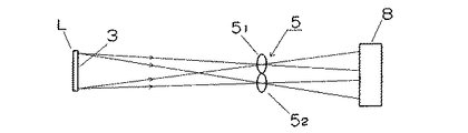
図1は同第1の実施の形態の斜視図、図2はその平面図、図3はその側面図、図4は被読取部材(例えばラベル)の平面図、そして、図5は被読取部材L上の線状反射領域3cの細部の説明図である。
図1〜3において、Lは被読取部材(例えばラベル)、5は集光光学系、51は第1の結像レンズ、52は第2の結像レンズ、8は二次元電子走査形読取センサである。(3、3c1、3c2については、後述する)。
【0017】
図4において、Lは被読取部材(例えばラベル)、3は被読取部材L上に記録された光学的パターン(例えばバーコードシンボル)、3cは光学的パターン3上に想定された線状反射領域である。
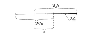
図5において、3c1は線条反射領域3c上に想定された第1の反射区域、3c2は同じく第2の反射区域、そして、dは第1の反射区域3c1と第2の反射区域3c1とが重複している区域重複部である。
図1に戻って再説するに、被読取部材Lの表面(図1では裏面は見えるが表面は見えない。)上に想定された線状反射領域3c、並びに、該線状反射領域3c上に想定された第1及び第2の反射区域3c1及び3c2が、破線によって、表されている。
【0018】
この実施の形態では、以上の諸要素の外に、増幅手段や信号2値化手段、メモリ手段、信号重複部解消手段、信号解読手段(デコード手段)が使用される(何れも無図示)。
二次元電子走査形読取センサ8の後段には、上記増幅手段が接続され、上記増幅手段の後段には、信号2値化手段が接続される。
上記のメモリ手段や、信号重複部解消手段、信号解読手段は、1個のマイクロコンピュータで構成することも出来る。
【0019】
(要素の構成及び要素間関係の詳細な説明)
二次元電子走査形読取センサ8は、図1では、2個の線状受光領域、即ち第1の線状受光領域81及び第2の線状受光領域82が、垂直面内において、互いに平行且つ水平に配置され、各線状受光領域81〜82には、無数のピクセル(画素)が水平方向に密に配列されている(無図示)。
この二次元電子走査形読取センサ8は、図2の如く、横長状に配設される。
集光光学系5は、図1〜3では、第1の結像レンズ51及び第2の結像レンズ52を含有する。そして、二次元電子走査形読取センサ8の前方に配置されている。
【0020】
以下においては、説明を簡単にするため、横幅が最大読取幅に達する光学的パターン3が、集光光学系5の前方に、略最大読取距離を隔てて、図1〜3の如く、横長状に置かれているものと仮定する。(このような仮定を置いても、この出願の発明の一般性が失われる虞(おそれ)はない。)
【0021】
第1の結像レンズ51の光軸は、かかる光学的パターン3上の線状反射領域3c(図1及び図4参照)と二次元電子走査形読取センサ8内の第1の線状受光領域81とを含む第1の平面内であって、しかも、第1の反射区域3c1の中心点から第1の線状受光領域81の中心点に到る反射光の光路内に配置される。
【0021】
第2の結像レンズ52の光軸は、上記線状反射領域3cと二次元電子走査形読取センサ8上の第2の線状受光領域82とを含む第2の平面内であって、しかも上記第2の反射区域3c2の中心点から上記第2の線状受光領域82の中心点に到る反射光の光路内に配置される。
かくの如くにして配列された第1及び第2の結像レンズ51及び52は、相互に接触又は衝突する虞無しとしない。そのような場合は、第1及び第2の結像レンズ51及び52を前後方向にずらすことによって、接触や衝突を簡単に回避することが出来る。
【0022】
(動作の説明)
光照射手段が光学的パターン3の全体を照射したとき、第1の反射区域3c1及び第2の反射区域3c2によってそれぞれ反射されて成る第1の光像及び第2の光像がそれぞれ、第1の結像レンズ51及び第2の結像レンズ52によって、第1の線状受光領域81及び第2の線状受光領域82上に結像せしめられる。
【0023】
第1の線状受光領域81及び第2の線状受光領域82の各ピクセル(画素)に光信号が入射すると、当該各ピクセルにおける光の強弱信号がそれぞれ信号電荷に光電変換され、当該信号電荷が蓄積され、当該各ピクセルに対してラスタ走査式の電子的走査がなされることによって、全ての信号電荷が時間軸上の一連の電気的アナログ信号に変換される。
上記一連の電気的アナログ信号は、信号2値化手段によって、一連の2値信号に変換される。
上記一連の2値信号は、好ましくは、メモリ手段に一旦記憶せしめられる。
【0024】
第1の反射区域3c1由来の2値信号と第2の反射区域3c2由来の2値信号とは、両者の重複部分(共通部分)が、上記信号重複部解消手段によって検出され、その一方が削除され、両信号が縮合されることによって、光学的パターン3に対応する真正2値信号に変換される。
いま、第1の反射区域3c1由来の2値信号列をB、その長さをM、第2の反射区域3c2由来の2値信号列をC、その長さをN、両信号列の重複部の長さをKとすれば、両信号列は、下記の如く、表される。
B=(B1,…,BM−K+1,…,BM)・・・・・・・・・・・(1)
C= …,….… (C1,…,CK,…,CN) ・・・・・・(2)
而して、重複部の両2値信号間には、下記K個の一致式が成り立つ。
BM−K+1=C1・・・・・・・・・・・・・・・・・・・・(3−1)
BM−K+i=Ci(但しi=2,3,…,K−1)・・・・・(3−2)
BM =CK・・・・・・・・・・・・・・・・・・・・(3−3)
式(3−1)〜(3−3)によれば、少なくともK個の一致回路と、K−1個のアンド回路を用意すれば、長さK個の信号重複部分を検出出来ることが明らかである。
上記真正2値信号は、信号解読手段(デコード手段)によって解読され、それによって元の情報、即ち光学的パターン3に担持された情報が復元される。
【0025】
(図1〜5の拡張)
図1の二次元電子走査形読取センサ8における、線状受光領域の個数2は、n個に拡張することが出来る。即ち、
拡張された二次元電子走査形読取センサ8は、n個の線条受光領域(但しnは2以上の整数)、即ち第1の線状受光領域81、第iの線状受光領域8i(但しi=2,3,…,n−1)、及び第nの線状受光領域8n(無図示)が、図1と同様に、垂直面内において互いに平行且つ水平に配置され、各線状受光領域81〜8nには、無数のピクセル(画素)が水平方向に密に配列される(無図示)こととなる。
【0026】
図1〜3の集光光学系5における結像レンズの個数2は、二次元電子走査形読取センサ8における線状受光領域の個数2と同様に、n個に拡張することが出来る。
拡張された集光光学系5は、n個の結像レンズ、即ち第1の結像レンズ51、第iの結像レンズ5i(但しi=2,3,…,n−1)、及び第nの結像レンズ5nを含有する(無図示)こととなる。
【0027】
拡張された線状反射領域3c上には、n個の反射区域が想定される。
第1の反射区域3c1は、その一端(例えば右端)が線状反射領域3cの一端(例えば右端)を含むと共に、その他端(例えば左端)の近傍が第2の反射区域3c2の一端(例えば右端)の近傍と重複する。
第iの反射区域3ci(但しi=2,3,…,n−1)は、その一端(例えば右端)の近傍が第i−1の反射区域3ci−1の他端(例えば左端)の近傍と重複すると共に、その他端(例えば左端)の近傍が第i+1の反射区域3ci+1の一端(例えば右端)の近傍と重複する。
第nの反射区域3cnは、第n−1の反射区域3cn−1に対して一端の近傍が重複すると共に、線状反射領域3cの他端を含む。
【0028】
拡張された集光光学系5における第iの結像レンズ5i(i=2,3,…,n−1)の光軸は、線状反射領域3cと第iの線状受光領域8iとを含む第iの平面内であって、しかも、第iの反射区域3ciの中心点から、反射ミラー4を介して、第iの線状受光領域8iの中心点に到る反射光の光路内に配置される(無図示)こととなる。
【0029】
拡張された集光光学系5における第nの結像レンズ5nの光軸は、線状反射領域3cと第nの線状受光領域8nとを含む第nの平面内であって、しかも、第nの反射区域3cnの中心点から、反射ミラー4を介して、第nの線状受光領域8nの中心点に到る反射光の光路内に配置される(無図示)こととなる。
その余の構成については、図1〜3と同様である。
【0030】
(拡張された動作)
光照射手段が光学的パターン3の全体を照射したとき、第1の反射区域3c1〜第nの反射区域3cnによってそれぞれ反射されて成る第1の光像〜第nの光像がそれぞれ、第1の結像レンズ51〜第nの結像レンズ5nによって、第1の線状受光領域81〜第nの線状受光領域8n上に結像せしめられる。
【0031】
その時、第1の線状受光領域81〜第nの線状受光領域8n上の各ピクセルにおける光の強弱信号がそれぞれ信号電荷に光電変換され、当該各信号電荷が各ピクセルに蓄積され、当該各ピクセルに対してラスタ走査式の電子的走査がなされることによって、全ての信号電荷が時間軸上の一連の電気的アナログ信号に変換される。
【0032】
ここでは、第1の反射区域3c1〜第nの反射区域3cn中の任意の反射区域は、第iの反射区域3ci(一般項)で代表される。その際、iには、順次、整数1,2,…,nが代入される。
第iの反射区域3ci由来の2値信号(但しi=1,2,…,n−1)と第i+1の反射区域3ci+1由来の2値信号とは、それらの重複部分(共通部分)が、信号重複部解消手段によって検出され、その一方が削除され、両信号が縮合されることによって、光学的パターン3に対応する真正2値信号に変換される。
上記信号重複部解消手段は、前述の如く、少なくともK個の一致回路と、K−1個のアンド回路とを含有するが、それらの回路は、反復して少なくともn−1回使用されることとなる。
その余の動作については、図1〜3の動作と同様である。
【0033】
〔第2の実施の形態〕
この出願の発明の光学的情報読取装置の第2の実施の形態について説明する。
同第2の実施の形態の光学的情報読取装置は、前記第1の実施の形態の光学的情報読取装置において、一の筐体を含有したものである。
上記筐体は、その内部に、前記集光光学系5、前記二次元電子走査形読取センサ8、前記信号2値化手段、及び前記信号重複部解消手段の全部又は主要部が収納される。
第2の実施の形態では、光照射手段は、上記筐体の内部又は外部に配置することが出来る。
第2の実施の形態のその余の事項は、第1の実施の形態と同様である。
【0034】
〔第3の実施の形態〕
この出願の発明の光学的情報読取装置の第3の実施の形態について説明する。同第3の実施の形態は、水平方向に読取口幅よりも長大な寸法を有する光学的パターンを読取るためのものである。
(構成要素の簡単な説明)
図6は、同第3の実施の形態の説明図であって、同図(a)は、筐体上部を除去して示す平面図、同図(b)は縦断面図である。
図6において、1は筐体、2は光照射手段、Lは被読取部材(例えばラベル)、3は被読取部材L上の光学的パターン、4は反射ミラー、5は集光光学系、51及び52は結像レンズ、8は二次元電子走査形読取センサである。
【0035】
この実施の形態では、以上の諸要素の外に、増幅手段や信号2値化手段、メモリ手段、信号重複部解消手段、信号解読手段(デコード手段)が使用される(何れも無図示)。
二次元電子走査形読取センサ8の後段には、上記増幅手段が接続され、上記増幅手段の後段には、信号2値化手段が接続される。
上記のメモリ手段や、信号重複部解消手段、信号解読手段は、1個のマイクロコンピュータで構成することも出来る。
【0036】
(要素の構成及び要素間関係の詳細な説明)
以下においては、説明の便のため、オペレータから見て、前後方向を縦方向、左右方向を横方向という。
筐体1は、縦方向(図6の紙面では左右方向)に即して、後部、中間部及び前部から成る。図6では、後部から中間部が水平部、前部が下降部(傾斜部)を成し、両部の境界近傍が湾曲部を成す。
筐体1の先端部には光出入口、内部には空洞が形成される。
上記水平部は、断面が長方形の角筒から成り、略水平に置かれている。
上記前部は、図示の如く、断面が長方形を成すと共に、より前方の横幅程大と成る、末広がり形(逆台形又は扇形)を成す。
上記水平部の形状は、断面が六角形の角筒形や、断面が円形の円筒形とすることも出来る。一般に、断面が任意の形状の筒形とすることが出来る。
【0037】
光照射手段2は、光出入口の前方に最大読取可能距離を隔てて横長状に置かれた光学的パターン3の全体を、照射するためのものである。図6では、4個の光源が、光出入口の内側近傍の一の線分の上に、等間隔を成して配列されている。
光照射手段2の光源の個数は、1〜3個とすることも出来るし、5個以上とすることも出来る。即ち、1〜複数個とすることが出来る。
光源の個数が複数個の場合は、その配列形状を、コの字状又はループ状とすることが出来る。
【0038】
反射ミラー4は、斜め下前方から到来する反射光を、略水平方向後ろ向きに偏向させるために、図6(b)の如く、湾曲点近傍の空洞内に、斜め下後ろ向きに配置される。ここに、反射ミラーの向きは、鏡面に立てた法線の向きによって表されるものとする。
そして、図6(a)の如く、横長状に配置される。
【0039】
二次元電子走査形読取センサ8は、n個の線状受光領域(但しnは2以上の整数)、即ち第1の線状受光領域81、第iの線状受光領域8i(但しi=2,3,…,n−1)、及び第nの線状受光領域8nが垂直面内において互いに平行且つ水平に配置され、各線状受光領域81〜8nには無数のピクセルが水平方向に密に配列されている。
二次元電子走査形読取センサ8の配設位置は、筐体1の後部における空洞の内部とされる。
集光光学系5は、n個の結像レンズ(nは2以上の整数)、即ち、第1の結像レンズ51、第iの結像レンズ5i(但しi=2,3,…,n−1)及び第nの結像レンズ5nを含有する。
【0040】
以下においては、説明を簡単にするため、横幅が最大読取幅に達する光学的パターン3が、前記光出入口の前方に、略最大読取可能距離Δを隔てて横長状に置かれているものと仮定する。
ここに、最大読取可能距離Δとは、集光光学系5から見た前記最大読取距離をD、集光光学系5と前記光出入口との距離をD0とすれば、
Δ=D−D0
によって与えられる。
【0041】
光学的パターン3上に線状反射領域3cが想定される。
線状反射領域3c上には、n個の反射区域、即ち、第1の反射区域3c1〜第nの反射区域3cnが想定される。
第1の反射区域3c1は、その一端(例えば右端)が線状反射領域3cの一端(例えば右端)を含むと共に、その他端(例えば左端)の近傍が第2の反射区域3c2の一端(例えば右端)の近傍と重複する。
【0042】
第2の反射区域3c2から第n−1の反射区域3cn−1までを、「第iの反射区域3ci(i=2,3,…,n−1)」で代表させたとき、
第iの反射区域3ci(i=2,3,…,n−1)は、その一端(例えば右端)の近傍が第i−1の反射区域3ci−1の他端(例えば左端)の近傍と重複する共に、その他端(例えば左端)の近傍が第i+1の反射区域3ci+1の一端(例えば右端)の近傍と重複する。
第nの反射区域3cnは、その一端(例えば右端)の近傍が第n−1の反射区域3cn−1の他端(例えば左端)の近傍と重複する共に、その他端(例えば左端)が線状反射領域3cの他端を含む。
【0043】
線状反射領域3cから到来し、反射ミラー4で略水平方向に偏向され、二次元電子走査形読取センサ8上の第1の線状受光領域81で受光される、略水平な反射光光束によって、第1の平面が規定される。
第1の結像レンズ51の光軸は、上記第1の平面内であって、しかも、第1の反射区域の中心点から、反射ミラー4を介して、第1の線状受光領域81の中心点に到る反射光の光路内に配置される。
【0044】
第2の結像レンズ52〜第n−1の結像レンズ5n−1を、「第iの結像レンズ5i(i=2,3,…,n−1)」で代表させたとき、
線状反射領域3cから到来し、反射ミラー4で略水平方向に偏向され、二次元電子走査形読取センサ8上の第iの線状受光領域8iで受光される、略水平な反射光光束によって、第iの平面が規定される。
第iの結像レンズ5i(i=2,3,…,n−1)の光軸は、上記第iの平面内であって、しかも、第iの反射区域の中心点から、反射ミラー4を介して、第iの線状受光領域8iの中心点に到る反射光の光路内に配置される。
【0045】
線状反射領域3cから到来し、反射ミラー4で略水平方向に偏向され、二次元電子走査形読取センサ8上の第nの線状受光領域8nで受光される、略水平な反射光光束によって、第nの平面が規定される。
第nの結像レンズ5nの光軸は、上記第nの平面内であって、しかも、第nの反射区域3cnの中心点から、反射ミラー4を介して、第nの線状受光領域8nの中心点に到る反射光の光路内に配置される。
前記信号2値化手段は、前記空洞内のその余の部位、即ち光照射手段2、反射ミラー4、集光光学系5及び二次元電子走査形読取センサ8の配設部位並びに照射光及び反射光の通過空間以外の部位に配置される。
前記信号重複部解消手段は、前記第1の実施の形態の信号重複部解消手段をn−1個含有して成るものであっても良いし、前記信号重複部解消手段の1個を、反復してn−1回適用するようにしたものであっても良い。
第3の実施の形態のその余の構成は、第1の実施の形態のそれと同様である。
【0046】
(動作の説明)
光照射手段2が光学的パターン3の全体を照射したとき、第1の反射区域3c1〜第nの反射区域3cnによってそれぞれ反射されて成る第1の光像〜第nの光像はそれぞれ、第1の結像レンズ51〜第nの結像レンズ5nによって、第1の線状受光領域81〜第nの線状受光領域8n上に結像せしめられる。
次いで、第1の線状受光領域81〜第nの線状受光領域8n上の各ピクセルにおける光の強弱信号がそれぞれ信号電荷に光電変換され、当該各信号電荷が当該各ピクセルに蓄積され、当該各ピクセルに対してラスタ走査式の電子的走査がなされることによって、全ての信号電荷が時間軸上の一連の電気的アナログ信号に変換される。
【0047】
上記一連の電気的アナログ信号は、上記信号2値化手段によって、一連の2値信号に変換される。
上記一連の2値信号は、上記信号重複部解消手段によって、重複信号の一方を削除され、且つ縮合されることによって、光学的パターン3に対応する真正2値信号に変換される。
第3の実施の形態のその余の動作は、第1の実施の形態のそれと同様である。
【0048】
〔第4の実施の形態〕
この出願の発明の光学的情報読取装置の第4の実施の形態について説明する。同第4の実施の形態の光学的情報読取装置は、前記第3の実施の形態の光照射手段2の光源の個数が複数個である場合において、光源の配設密度が、前記光出入口の左端部又は右端部に近付くに連れて大とされて成るものである。
上記光源のこのような配設密度によれば、筐体1の光出入口の横幅を超える長大な横幅を有する光学的パターン3が同光出入口の前方に最大読取可能距離を隔てて横長状に置かれたような場合であっても、同光学的パターン3における光出入口の横幅を超える部分の照度を特に大とすることが出来る。
これによって、上記光出入口の横幅の外方に位置する線状反射領域からの反射光の強度を、当該線状反射領域の中央部からの反射光の強度と同程度に成る様、増大させることが出来る。
【0049】
【発明の効果】
この出願の発明は、以上のように構成したから、下記(a)〜(f)の通り、顕著な効果を奏することが出来る。
(a)読取桁方向に種々なる長さを持つ各種の光学的パターンを、単独で読取ることが出来る。
(b)読取桁方向に方向に長大な長さを有する光学的パターンを、光出入口の幅が狭くて、小型の筐体で読み取ることが出来る。
(c)読取桁方向に長大な長さを有する光学的パターンを、1個同一の広角結像レンズを使用したものに比べて、歪み(ゆがみ)が少なく、高分解能で読取ることが出来る。
そして、操作性も良好である。
(d)読取桁方向に長大な長さを有する一段バーコードや多段バーコード、文字、記号等の光学的パターンを、正確に且つ高速で読取ることが出来る。
(e)表面が柔らかく且つ不定形を成す被読取部材や、表面が硬く且つ曲面状を成す被読取部材のバーコードシンボルについても誤読の虞が無く、従って読取り作業が効率的となる。
(f)従って、バーコードリーダを入力手段として使用する大型システムの構築が容易に成る。
【図面の簡単な説明】
【図1】この出願の発明の光学的情報読取装置の第1の実施の形態の要部の斜視図である。
【図2】同第1の実施の形態の要部の平面図である。
【図3】同第1の実施の形態の要部の側面図である。
【図4】被読取部材(例えばラベル)の平面図である。
【図5】被読取部材上の線状反射領域3cの細部の説明図である。
【図6】この出願の発明の光学的情報読取装置の第3の実施の形態の説明図である。
【符号の説明】
1 筐体
2 光照射手段
3 光学的パターン
3c 線状反射領域
3c1 第1の反射区域
3c2 第2の反射区域
4 反射ミラー
5 集光光学系
51 第1の結像レンズ
52 第2の結像レンズ
8 二次元電子走査形読取センサ
81 第1の線状受光領域
82 第2の線状受光領域
d 区域重複部
L 被読取部材(ラベル)[0001]
BACKGROUND OF THE INVENTION
The invention of this application relates to an optical information reading apparatus capable of reading optical information such as a barcode having a large number of digits and a wide width.
In particular, the present invention relates to an electronic scanning optical information reading apparatus capable of reading optical information such as a barcode having a long width exceeding the barcode reading port width and a large number of digits.
[0002]
[Prior art]
Prior art will be described.
Conventional optical information readers are roughly classified into three types: a touch scanner, a pen scanner, and a laser scanner.
A conventional touch scanner illuminates an optical pattern recorded on an optical recording medium (a member to be read) with illumination means,
An optical image formed by scattering and reflection from the optical pattern is formed on a one-dimensional electronic scanning type reading sensor (for example, CCD), and this is formed on the time axis by the photoelectric conversion function of the one-dimensional electronic scanning type reading sensor. To an electrical analog signal
This signal is processed electrically to read the optical pattern.
As the optical pattern, bar code symbols have been mainly used.
Further, as an optical recording medium (a member to be read), a member having a generally hard and flat surface has been used.
[0003]
However, as the field of product information registration processing and information management expands to retail, FA (Factor Automation), distribution, service industry, OA (Office Automation), etc., the types of goods and information handled are diversified. The amount of information has been increasing.
As a result, some notable changes occurred.
First, as the amount of information increases, the maximum number of digits of barcode symbols increases. Some of the members to be read (for example, labels) have a length in the reading digit direction ranging from 15 cm to 20 cm.
[0004]
Secondly, as the optical recording medium (read member), a member having a hard surface and a curved surface, and a member having a soft surface and an indefinite shape have been used.
For example, a label on which a barcode symbol is printed is attached to the surface of a bag or can, or the barcode symbol itself is directly printed on the surface of a bag or can.
[0005]
Third, coupled with the development of the barcode system, barcode symbols such as JAN, EAN, UPC attached to soft materials on the surface such as bags in retail, FA, OA, and logistics applications, and Code39 , Code128, NW7, ITF, etc., bar code symbols with indefinite length are mixed.
[0006]
[Problems of the prior art]
First, in order to make it possible to read a long optical pattern in the reading digit direction with the conventional touch scanner, the width of the reading port must be made long.
However, a touch-type scanner with a wide reading port width naturally has a poor operability.
[0007]
Second, in the conventional type touch scanner with a long reading port width, the horizontal width of the one-dimensional electronic scanning type reading sensor is limited by itself, so that a short focal length and a wide-angle image are required. It becomes.
However, when a wide-angle lens is used with a short focal length and a wide-angle lens, a distortion aberration (distortion aberration) peculiar to the wide-angle lens is generated. Therefore, an optical image (image formation) on a one-dimensional electronic scanning type reading sensor. , The similarity with the original optical pattern is impaired (see Iwanami "Science and Chemistry Dictionary 4th Edition" (issued on December 15, 1989), page 473, "Seidel's Five Aberrations").
[0008]
Third, when using a conventional touch type scanner with a wide reading aperture and a short focal length and wide angle imaging, the number of pixels on the one-dimensional electronic scanning type reading sensor However, the resolution and the reading accuracy are reduced and the result is limited.
[0009]
Fourth, while the tip of the Ben type scanner is in contact with the barcode symbol of the member to be read whose surface has a soft and irregular shape, or the member to be read whose surface has a hard surface and a curved surface, and while maintaining constant Scanning at speed has never been easy for many operators. This is even more so when the barcode symbol becomes longer. For this reason, there are many misreads of bar code information, so that the reading operation becomes inefficient.
[0010]
Fifth, in order to read a bar code symbol having an indefinite length, a pen type scanner and a touch type scanner are prepared in advance. There is a way to use differently,
This method has a problem that the initial cost and the running cost are increased to always have two types of scanners, and therefore to enable the connection change to the host computer at all times. In addition, how to use the both is very complicated for many operators.
Sixth, due to the existence of the above problems, a major bottleneck has occurred in further system scale-up.
[0011]
OBJECT OF THE INVENTION
Therefore, a first object of the invention of this application is to provide an optical information reader capable of independently reading various optical patterns having a length in an arbitrary reading digit direction.
The second object of the invention of this application is to read an optical pattern that is long in the reading digit direction with less resolution (distortion) and higher resolution than that using a single wide-angle imaging lens. It is possible to provide an optical information reading apparatus that can perform the above operation and has good operability.
A third object of the invention of this application is to provide an optical information reader capable of accurately and rapidly reading an optical pattern such as a one-stage bar code, a multi-stage bar code, characters and symbols that are long in the reading digit direction. Is to provide.
[0012]
[Means for achieving the objectives]
In order to solve the above-mentioned problems and achieve the above-mentioned objects, an optical information reader according to a first aspect of the invention of this application includes:
A light irradiating means, a condensing
The two-dimensional electronic scanning
The condensing
The
A linear reflection region 3c is assumed on the
On the linear reflection region 3c, n reflection regions, that is, a first reflection region 3c including one end of the linear reflection region 3c.1, I-1th reflective area 3ci-1(Where i = 2, 3,..., N−1), the i-th reflective area 3c where the vicinity of one end overlaps.i, And the (n-1) th reflective area 3cn-1And the vicinity of one end overlaps the nth reflection area 3c including the other end of the linear reflection region 3c.nIs assumed,
I-
Therefore, when the light irradiating means irradiates the entire
Next, the first linear
The series of electrical analog signals are converted into a series of binary signals by the signal binarization means,
The series of binary signals is converted into a true binary signal corresponding to the
Is.
[0013]
The optical information reader of the second aspect of the invention of this application is:
In the optical information reader of the first embodiment, containing one housing,
The casing houses therein all or main parts of the condensing
Is.
[0014]
The optical information reader of the third aspect of the invention of this application is:
A housing 1, a light irradiation means 2, a reflection mirror 4, a condensing
The housing 1 has a horizontal cylindrical shape from the rear to the middle, a front widened to the end, a horizontal portion up to the middle curved point, a lower portion from the curved point, and a tip. A light entrance and exit is formed in the part, and a cavity is formed inside,
The light irradiating means 2 is composed of one or a plurality of light sources, and these light sources can irradiate the entire
The reflection mirror 4 is disposed obliquely downward and rearward in the cavity near the bending point in order to deflect the reflected light arriving from obliquely downward and forward in a substantially horizontal direction,
The two-dimensional electronic scanning
The condensing
The
A linear reflection region 3c is assumed on the
On the linear reflection region 3c, n reflection regions, that is, a first reflection region 3c including one end of the linear reflection region 3c.1, I-1th reflective area 3ci-1(Where i = 2, 3,..., N−1), the i-th reflective area 3c where the vicinity of one end overlaps.i, And the (n-1) th reflective area 3cn-1And the vicinity of one end overlaps the nth reflection area 3c including the other end of the linear reflection region 3c.nIs assumed,
I-
The signal binarizing means is disposed in the remaining part of the cavity,
Therefore, when the light irradiation means 2 irradiates the entire
Next, the first linear
The series of electrical analog signals are converted into a series of binary signals by the signal binarization means,
The series of binary signals is converted into a true binary signal corresponding to the
Is.
[0015]
The optical information reader of the fourth aspect of the invention of this application is:
When the
Is.
[0016]
DETAILED DESCRIPTION OF THE INVENTION
[First Embodiment]
A first embodiment of the optical information reading device of the invention of this application will be described.
The first embodiment is for reading optical patterns having various lengths.
(A brief description of the components)
1 is a perspective view of the first embodiment, FIG. 2 is a plan view thereof, FIG. 3 is a side view thereof, FIG. 4 is a plan view of a member to be read (for example, a label), and FIG. It is explanatory drawing of the detail of the linear reflective area | region 3c on L. FIG.
1-3, L is a member to be read (for example, a label), 5 is a condensing optical system, 51Is the first imaging lens, 52Is a second imaging lens, and 8 is a two-dimensional electronic scanning reading sensor. (3, 3c13c2Will be described later).
[0017]
In FIG. 4, L is a member to be read (for example, a label), 3 is an optical pattern (for example, a bar code symbol) recorded on the member to be read L, and 3 c is a linear reflection region assumed on the
In FIG. 5, 3c1Is the first reflection area 3c assumed on the line reflection region 3c.2Is also the second reflective area, and d is the first reflective area 3c1And the second reflection area 3c1It is the area overlap part where and overlap.
Returning to FIG. 1 again, the linear reflection region 3c assumed on the surface of the read member L (the back surface is visible but the front surface is not visible in FIG. 1), and the linear reflection region 3c are assumed. Assumed first and second reflective areas 3c1And 3c2Is represented by a broken line.
[0018]
In this embodiment, in addition to the above elements, an amplifying means, a signal binarizing means, a memory means, a signal duplication canceling means, and a signal decoding means (decoding means) are used (all not shown).
The amplification means is connected to the subsequent stage of the two-dimensional electronic scanning
The memory means, the signal duplication part eliminating means, and the signal decoding means can be constituted by a single microcomputer.
[0019]
(Detailed description of element structure and inter-element relationship)
In FIG. 1, the two-dimensional electronic scanning
The two-dimensional electronic scanning
The condensing
[0020]
In the following, for the sake of simplicity, the
[0021]
[0021]
The first and
[0022]
(Description of operation)
When the light irradiation means irradiates the entire
[0023]
First linear
The series of electrical analog signals are converted into a series of binary signals by signal binarization means.
The series of binary signals are preferably stored once in the memory means.
[0024]
1st reflective area 3c1Derived binary signal and second reflective area 3c2The derived binary signal corresponds to the
Now, the first reflective area 3c1The binary signal sequence derived from B is B, its length is M, and the second reflection area 3c2If the derived binary signal sequence is C, the length is N, and the length of the overlapping portion of both signal sequences is K, both signal sequences are expressed as follows.
B = (B1, ..., BM-K + 1, ..., BM(1)
C = ..., ... ... (C1, ..., CK, ..., CN(2)
Thus, the following K coincidence equations are established between both binary signals in the overlapping portion.
BM-K + 1= C1 ... (3-1)
BM-K + i= Ci(Where i = 2, 3,..., K-1) (3-2)
BM = CK........................... (3-3)
According to the equations (3-1) to (3-3), it is clear that if at least K matching circuits and K-1 AND circuits are prepared, K overlapping signal portions can be detected. It is.
The genuine binary signal is decoded by a signal decoding means (decoding means), whereby the original information, that is, the information carried on the
[0025]
(Expansion of Figs. 1-5)
In the two-dimensional electronic scanning
The expanded two-dimensional electronic scanning
[0026]
The number of
The expanded condensing
[0027]
On the extended linear reflection region 3c, n reflection areas are assumed.
1st reflective area 3c1The one end (for example, the right end) includes one end (for example, the right end) of the linear reflection region 3c, and the vicinity of the other end (for example, the left end) is the second reflection area 3c.2It overlaps with the vicinity of one end (for example, the right end).
I-th reflective area 3ci(Where i = 2, 3,..., N−1) is in the vicinity of one end (for example, the right end) of the i−1th reflection area 3c.i-1And the vicinity of the other end (for example, the left end) is the i + 1th reflection area 3c.i + 1It overlaps with the vicinity of one end (for example, the right end).
Nth reflective area 3cnIs the (n-1) th reflective area 3cn-1, The vicinity of one end overlaps, and the other end of the linear reflection region 3c is included.
[0028]
The i-
[0029]
The
The remaining configuration is the same as in FIGS.
[0030]
(Extended behavior)
When the light irradiation means irradiates the entire
[0031]
At that time, the first linear
[0032]
Here, the first reflective area 3c1-Nth reflection area 3cnAny reflective area in the i-th reflective area 3ci(General terms) At that time,
I-th reflective area 3ciBinary signal (where i = 1, 2,..., N−1) and i + 1th reflection area 3ci + 1The binary signal derived from the signal is the authenticity corresponding to the
As described above, the signal duplication canceling means includes at least K matching circuits and K-1 AND circuits, which are repeatedly used at least n-1 times. It becomes.
The other operations are the same as those shown in FIGS.
[0033]
[Second Embodiment]
A second embodiment of the optical information reading device of the invention of this application will be described.
The optical information reading device of the second embodiment is the same as the optical information reading device of the first embodiment, but includes one housing.
The housing houses all or the main part of the condensing
In the second embodiment, the light irradiation means can be disposed inside or outside the casing.
The remaining items of the second embodiment are the same as those of the first embodiment.
[0034]
[Third Embodiment]
A third embodiment of the optical information reading device of the invention of this application will be described. The third embodiment is for reading an optical pattern having a dimension longer than the reading port width in the horizontal direction.
(A brief description of the components)
6A and 6B are explanatory views of the third embodiment, in which FIG. 6A is a plan view in which the upper part of the housing is removed, and FIG. 6B is a longitudinal sectional view.
In FIG. 6, 1 is a housing, 2 is a light irradiation means, L is a member to be read (for example, a label), 3 is an optical pattern on the member to be read L, 4 is a reflecting mirror, 5 is a condensing optical system, 51And 52Is an imaging lens, and 8 is a two-dimensional electronic scanning type reading sensor.
[0035]
In this embodiment, in addition to the above elements, an amplifying means, a signal binarizing means, a memory means, a signal duplication canceling means, and a signal decoding means (decoding means) are used (all not shown).
The amplification means is connected to the subsequent stage of the two-dimensional electronic scanning
The memory means, the signal duplication part eliminating means, and the signal decoding means can be constituted by a single microcomputer.
[0036]
(Detailed description of element structure and inter-element relationship)
In the following, for convenience of explanation, the front-rear direction is referred to as the vertical direction and the left-right direction is referred to as the horizontal direction as viewed from the operator.
The housing 1 is composed of a rear portion, an intermediate portion, and a front portion in accordance with the vertical direction (the left-right direction in the drawing of FIG. 6). In FIG. 6, the middle part from the rear part forms a horizontal part, the front part forms a descending part (inclined part), and the vicinity of the boundary between both parts forms a curved part.
A light entrance / exit is formed at the tip of the housing 1 and a cavity is formed inside.
The horizontal portion is formed of a rectangular tube having a rectangular cross section, and is placed substantially horizontally.
As shown in the drawing, the front part has a rectangular cross section and a divergent shape (inverted trapezoidal shape or fan shape) that has a larger front width.
The shape of the horizontal portion may be a rectangular tube having a hexagonal cross section or a cylindrical shape having a circular cross section. Generally, the cross section can be a cylindrical shape having an arbitrary shape.
[0037]
The light irradiation means 2 is for irradiating the entire
The number of light sources of the light irradiation means 2 can be 1 to 3, or 5 or more. That is, the number can be one or more.
When there are a plurality of light sources, the array shape can be a U-shape or a loop shape.
[0038]
The reflection mirror 4 is disposed obliquely downward and rearward in a cavity near the inflection point, as shown in FIG. 6B, in order to deflect reflected light arriving from the obliquely lower front in a substantially horizontal rearward direction. Here, the direction of the reflection mirror is represented by the direction of the normal line upright on the mirror surface.
And it arrange | positions horizontally long like FIG. 6A.
[0039]
The two-dimensional electronic scanning
The arrangement position of the two-dimensional electronic scanning
The condensing
[0040]
In the following, for the sake of simplicity, it is assumed that the
Here, the maximum readable distance Δ is the maximum reading distance as viewed from the condensing optical system D, and the distance between the condensing
Δ = D−D0
Given by.
[0041]
A linear reflection region 3 c is assumed on the
On the linear reflection region 3c, n reflection areas, that is, the first reflection area 3c.1-Nth reflection area 3cnIs assumed.
1st reflective area 3c1The one end (for example, the right end) includes one end (for example, the right end) of the linear reflection region 3c, and the vicinity of the other end (for example, the left end) is the second reflection area 3c.2It overlaps with the vicinity of one end (for example, the right end).
[0042]
Second reflection area 3c2To (n-1) th reflection area 3cn-1Up to "i-th reflective area 3ci(I = 2, 3, ..., n-1) "
I-th reflective area 3ci(I = 2, 3,..., N−1) is in the vicinity of one end (for example, the right end) of the i−1th reflection area 3ci-1And the vicinity of the other end (for example, the left end) is the i + 1th reflection area 3c.i + 1It overlaps with the vicinity of one end (for example, the right end).
Nth reflective area 3cnIs near the one end (for example, the right end) of the n-1th reflection area 3c.n-1The other end (for example, the left end) includes the other end of the linear reflection region 3c.
[0043]
The first linear
[0044]
Second imaging lens 52-N-
Due to the substantially horizontal reflected light beam that arrives from the linear reflection region 3c, is deflected in a substantially horizontal direction by the reflection mirror 4, and is received by the i-th linear light reception region 8i on the two-dimensional electronic scanning read
The optical axis of the i-th imaging lens 5i (i = 2, 3,..., N−1) is in the i-th plane, and from the center point of the i-th reflection area, the reflection mirror 4 Through the i-th linear
[0045]
The n-th linear
The signal binarizing means includes the remaining part in the cavity, that is, the light irradiating means 2, the reflecting mirror 4, the condensing
The signal duplication part elimination unit may include n-1 signal duplication part elimination units of the first embodiment, or one of the signal duplication part elimination units is repeated. Then, it may be applied n-1 times.
The remaining configuration of the third embodiment is the same as that of the first embodiment.
[0046]
(Description of operation)
When the light irradiation means 2 irradiates the entire
Next, the first linear
[0047]
The series of electrical analog signals are converted into a series of binary signals by the signal binarization means.
The series of binary signals are converted into genuine binary signals corresponding to the
The remaining operation of the third embodiment is the same as that of the first embodiment.
[0048]
[Fourth Embodiment]
A fourth embodiment of the optical information reader according to the invention of this application will be described. In the optical information reading apparatus according to the fourth embodiment, when the number of light sources of the light irradiation means 2 according to the third embodiment is plural, the arrangement density of the light sources is set at the light entrance / exit. It is made larger as it approaches the left end or the right end.
According to such an arrangement density of the light sources, the
Thus, the intensity of the reflected light from the linear reflection area located outside the lateral width of the light entrance is increased so as to be approximately the same as the intensity of the reflected light from the central portion of the linear reflection area. I can do it.
[0049]
【The invention's effect】
Since the invention of this application is configured as described above, significant effects can be achieved as described in the following (a) to (f).
(A) Various optical patterns having various lengths in the reading digit direction can be read independently.
(B) An optical pattern having a long length in the direction of the reading digit can be read by a small casing with a narrow light exit / entrance width.
(C) An optical pattern having a long length in the reading digit direction can be read with a high resolution with less distortion (distortion) as compared with one using one identical wide-angle imaging lens.
And operability is also good.
(D) Optical patterns such as single-stage barcodes, multi-stage barcodes, characters and symbols having a long length in the reading digit direction can be read accurately and at high speed.
(E) There is no possibility of erroneous reading with respect to a member to be read having a soft surface and an indeterminate shape, and a barcode symbol of a member to be read having a hard surface and a curved surface, so that the reading operation becomes efficient.
(F) Therefore, it is easy to construct a large system that uses a bar code reader as an input means.
[Brief description of the drawings]
FIG. 1 is a perspective view of an essential part of a first embodiment of an optical information reading apparatus according to the present invention.
FIG. 2 is a plan view of a main part of the first embodiment.
FIG. 3 is a side view of the main part of the first embodiment.
FIG. 4 is a plan view of a member to be read (for example, a label).
FIG. 5 is an explanatory diagram of details of a linear reflection region 3c on a member to be read.
FIG. 6 is an explanatory diagram of a third embodiment of the optical information reading device of the invention of this application.
[Explanation of symbols]
1 housing
2 Light irradiation means
3 Optical pattern
3c linear reflection area
3c1 First reflective area
3c2 Second reflection area
4 Reflection mirror
5 Condensing optical system
51 First imaging lens
52 Second imaging lens
8 Two-dimensional electronic scanning sensor
81 First linear light receiving region
82 Second linear light receiving area
d Area overlap part
L Member to be read (label)
Claims (4)
光照射手段と、集光光学系(5)と、二次元電子走査形読取センサ(8)と、信号2値化手段と、信号重複部解消手段とを含有し、
上記二次元電子走査形読取センサ(8)は、第1の線状受光領域(8 1 )、第iの線状受光領域(8 i )(但しi=2,3,…,n−1)、及び第nの線状受光領域(8 n )からなるn個の線状受光領域(但しnは2以上の整数)が垂直面内において互いに平行且つ水平に配置され、該各線状受光領 m域(81〜8n)には複数のピクセルが水平方向に配列されておって、全体として横長状に配設され、
上記集光光学系(5)は、第1の結像レンズ(51)、第iの結像レンズ(5i)(但しi=2,3,…,n−1)及び第nの結像レンズ(5n)のn個の結像レンズを含有しておって、上記二次元電子走査形読取センサ(8)の前方に配置され、
横幅が最大読取幅に達する光学的パターン(3)が、上記集光光学系(5)の前方に、略最大読取距離を隔てて横長状に置かれ、
該光学的パターン(3)上に線状反射領域(3c)が想定され、
該線状反射領域(3c)上に、該線状反射領域(3 c )の端部を含む第1の反射区域(3 c1 )、第i−1の反射区域(3 ci-1 )(但しi=2,3,…,n−1)に対して一端の近傍が重複する第iの反射区域(3 ci )、及び第n−1の反射区域(3 cn-1 )に対して一端の近傍が重複すると共に上記線状反射領域(3 c )の他端を含む第nの反射区域(3 cn )からなるn個の反射区域が想定されているとき、
上記第1の結像レンズ(51)の光軸は、上記線状反射領域(3c)と上記第1の線状受光領域(81)とを含む第1の平面内であって、しかも、上記第1の反射区域(3c1)の中心点から上記第1の線状受光領域(81)の中心点に到る反射光の光路内に配置され、
上記第iの結像レンズ(5i)(但しi=2,3,…,n−1)の光軸は、上記線状反射領域(3c)と上記第iの線状受光領域(8i)とを含む第iの平面内であって、しかも、上記第iの反射区域(3ci)の中心点から上記第iの線状受光領域(8i)の中心点に到る反射光の光路内に配置され、
上記第nの結像レンズ(5n)の光軸は、上記線状反射領域(3c)と上記第nの線状受光領域(8n)とを含む第nの平面内であって、しかも、上記第nの反射区域(3cn)の中心点から上記第nの線状受光領域(8n)の中心点に到る反射光の光路内に配置され、
以って、上記光照射手段が上記光学的パターン(3)の全体を照射したとき、上記第1の反射区域(3c1)〜第nの反射区域(3cn)によってそれぞれ反射されて成る第1の光像〜第nの光像がそれぞれ、上記第1の結像レンズ(51)〜第nの結像レンズ(5n)によって、上記第1の線状受光領域(81)〜第nの線状受光領域(8n)上に結像せしめられ、
次いで、上記第1の線状受光領域(81)〜第nの線状受光領域(8n)上の各ピクセルにおける光の強弱信号がそれぞれ信号電荷に光電変換され、当該信号電荷が蓄積され、当該各ピクセルに対してラスタ走査式の電子的走査がなされることによって、上記全ての信号電荷が時間軸上の一連の電気的アナログ信号に変換され、
上記一連の電気的アナログ信号が、上記信号2値化手段によって、一連の2値信号に変換され、上記一連の2値信号が、上記信号重複部解消手段によって、重複信号の一方を削除され、且つ縮合されることによって、上記光学的パターン(3)に対応する真正2値信号に変換される、
光学的情報読取装置。An optical information reader capable of reading optical patterns having various lengths,
A light irradiating means, a condensing optical system (5), a two-dimensional electronic scanning type reading sensor (8), a signal binarizing means, and a signal overlapping part eliminating means,
The two-dimensional electronic scanning type reading sensor (8), a first linear light-receiving region (81), the linear light receiving region of the i (8 i) (where i = 2,3, ..., n- 1) N linear light receiving regions (where n is an integer of 2 or more) made up of the nth linear light receiving regions (8 n ) are arranged in parallel and horizontally in the vertical plane, and each linear light receiving region m the band (8 1 ~8 n) weaving a plurality of pixels are arranged in the horizontal direction, are arranged in a horizontally long shape as a whole,
The condensing optical system (5) includes a first imaging lens (5 1 ), an i-th imaging lens (5 i ) (where i = 2, 3,..., N−1) and an n-th coupling. Containing n imaging lenses of the image lens (5 n ), disposed in front of the two-dimensional electronic scanning read sensor (8),
An optical pattern (3) whose horizontal width reaches the maximum reading width is placed in a horizontally long shape with a substantially maximum reading distance in front of the condensing optical system (5),
A linear reflection region (3 c ) is assumed on the optical pattern (3),
On the linear reflection region (3 c ), the first reflection area (3 c1 ) including the end of the linear reflection region (3 c ), the i- 1th reflection area (3 ci-1 ) ( However, i = 2, 3,..., N−1), one end of the i-th reflection area (3 ci ) whose one end overlaps, and one end of the n−1-th reflection area (3 cn−1 ). And n reflection areas consisting of the nth reflection area (3 cn ) including the other end of the linear reflection region (3 c ) are assumed.
The optical axis of the first imaging lens (5 1 ) is in a first plane including the linear reflection region (3 c ) and the first linear light receiving region (8 1 ), Moreover, disposed in the first reflection section (3 c1) the first linear from the center point of the light-receiving region (81) the optical path of the reflected light reaching the center point of,
The optical axis of the i- th imaging lens (5 i ) (where i = 2, 3,..., N−1) is such that the linear reflection region (3 c ) and the i-th linear light-receiving region (8 i ) and the reflected light from the central point of the i-th reflective area (3 ci ) to the central point of the i-th linear light receiving region (8 i ) In the optical path of
The optical axis of the n-th imaging lens (5 n ) is in the n-th plane including the linear reflection region (3 c ) and the n-th linear light-receiving region (8 n ), Moreover, it is disposed in the optical path of the reflected light from the center point of the nth reflection area (3 cn ) to the center point of the nth linear light receiving region (8 n ),
Therefore, when the light irradiating means irradiates the entire optical pattern (3), the first reflection area (3 c1 ) to the nth reflection area (3 cn ) are reflected by the first reflection area (3 c1 ) to the nth reflection area (3 cn ). 1 of the optical image of the optical image to the n, respectively, by the first imaging lens (5 1) to the n-th of the imaging lens (5 n), said first linear light-receiving region (81) - An image is formed on the nth linear light receiving region (8 n ),
Next, the light intensity signal in each pixel on the first linear light receiving region (8 1 ) to the n th linear light receiving region (8 n ) is photoelectrically converted into signal charges, and the signal charges are accumulated. By performing raster scanning electronic scanning for each pixel, all the signal charges are converted into a series of electrical analog signals on the time axis,
The series of electrical analog signals are converted into a series of binary signals by the signal binarization means, and the series of binary signals are deleted by the signal duplication portion elimination means, and one of the duplicate signals is deleted. And by being condensed, it is converted into a true binary signal corresponding to the optical pattern (3).
Optical information reader.
上記筐体は、その内部に、前記集光光学系(5)、前記二次元電子走査形読取センサ(8)、前記信号2値化手段、及び前記信号重複部解消手段の全部又は主要部が収納される、
光学的情報読取装置。The optical information reading device according to claim 1, comprising a case.
The casing includes in its interior all or main parts of the condensing optical system (5), the two-dimensional electronic scanning type reading sensor (8), the signal binarization means, and the signal duplication part elimination means. Stowed,
Optical information reader.
筐体(1)と、光照射手段(2)と、反射ミラー(4)と、集光光学系(5)と、二次元電子走査形読取センサ(8)と、信号2値化手段と、信号重複部解消手段とを含有し、
上記筐体(1)は、後部から中間部が水平筒形を成し、前部が末広がり形を成すと共に、途中の湾曲点迄は水平部、同湾曲点から先は下降部を成し、且つ、先端部に光出入口、内部に空洞が形成され、
上記光照射手段(2)は、1又は複数個の光源からなり、且つ、それらの光源は、上記光出入口の前方に最大読取可能距離を隔てて横長状に置かれた光学的パターン(3)の全体を照射可能にするために、同光出入口の内側近傍に点状、線分状、コの字状又はループ状に配列され、
上記反射ミラー(4)は、斜め下前方から到来する反射光を略水平方向に偏向させるために、上記湾曲点近傍の空洞内に、斜め下後ろ向きに配置され、
上記二次元電子走査形読取センサ(8)は、第1の線状受光領域(8 1 )、第iの線状受光領域(8 i )(但しi=2,3,…,n−1)、及び第nの線状受光領域(8 n )からなるn個の線状受光領域(但しnは2以上の整数)が垂直面内において互いに平行且つ水平に配置され、該各線状受光領域(81〜8n)には複数のピクセルが水平方向に密に配列されたものであって、上記筐体(1)の後部の空洞内に配置され、
上記集光光学系(5)は、第1の結像レンズ(5 1 )、第iの結像レンズ(5 i )(但しi=2,3,…,n−1)及び第nの結像レンズ(5 n )からなるn個の結像レンズを含有し、
横幅が最大読取幅に達する光学的パターン(3)が、上記集光光学系(5)の前方に、略最大読取距離を隔てて横長状に置かれ、
該光学的パターン(3)上に線状反射領域(3c)が想定され、
該線状反射領域(3c)上に、該線状反射領域(3 c )の一端を含む第1の反射区域(3 c1 )、第i−1の反射区域(3 ci-1 )(但しi=2,3,…,n−1)に対して一端の近傍が重複する第iの反射区域(3 ci )、及び第n−1の反射区域(3 cn-1 )に対して一端の近傍が重複すると共に上記線状反射領域(3 c )の他端を含む第nの反射区域(3 cn )からなるn個の反射区域が想定されているとき、
上記第1の結像レンズ(51)の光軸は、上記線状反射領域(3c)から到来し、上記反射ミラー(4)で略水平方向に偏向され、上記二次元電子走査形読取センサ(8)上の第1の線状受光領域(81)で受光される、略水平な反射光光束によって規定される、第1の平面内であって、しかも、上記第1の反射区域(3c1)の中心点から、上記反射ミラー(4)を介して、上記第1の線状受光領域(81)の中心点に到る反射光の光路内に配置され、
上記第iの結像レンズ(5i)(但しi=2,3,…,n−1)の光軸は、上記線状反射領域(3c)から到来し、上記反射ミラー(4)で略水平方向に偏向され、上記二次元電子走査形読取センサ(8)上の第iの線状受光領域(8i)で受光される、略水平な反射光光束によって規定される、第iの平面内であって、しかも、上記第iの反射区域(3c1)の中心点から、上記反射ミラー(4)を介して、上記第iの線状受光領域(8i)の中心点に到る反射光の光路内に配置され、
上記第nの結像レンズ(5n)の光軸は、上記線状反射領域(3c)から到来し、上記反射ミラー(4)で略水平方向に偏向され、上記二次元電子走査形読取センサ(8)上の第nの線状受光領域(8n)で受光される、略水平な反射光光束によって規定される、第nの平面内であって、しかも、上記第nの反射区域(3cn)の中心点から、上記反射ミラー(4)を介して、上記第nの線状受光領域(8n)の中心点に到る反射光の光路内に配置され、
上記信号2値化手段は、上記空洞内のその余の部位に配置され、
以って、上記光照射手段(2)が上記光学的パターン(3)の全体を照射したとき、上記第1の反射区域(3c1)〜第nの反射区域(3cn)によってそれぞれ反射されて成る第1の光像〜第nの光像がそれぞれ、上記第1の結像レンズ(51)〜第nの結像レンズ(5n)によって、上記第1の線状受光領域(81)〜第nの線状受光領域(8n)上に結像せしめられ、
次いで、上記第1の線状受光領域(81)〜第nの線状受光領域(8n)上の各ピクセルにおける光の強弱信号がそれぞれ信号電荷に光電変換され、当該信号電荷が蓄積され、当該各ピクセルに対してラスタ走査式の電子的走査がなされることによって、上記全ての信号電荷が時間軸上の一連の電気的アナログ信号に変換され、
上記一連の電気的アナログ信号が、上記信号2値化手段によって、一連の2値信号に変換され、
上記一連の2値信号が、上記信号重複部解消手段によって、重複信号の一方を削除され、且つ縮合されることによって、上記光学的パターン(3)に対応する真正2値信号に変換される、
光学的情報読取装置。An optical information reader capable of reading an optical pattern having a long dimension in the horizontal direction,
A housing (1), a light irradiation means (2), a reflection mirror (4), a condensing optical system (5), a two-dimensional electronic scanning sensor (8), a signal binarization means, Including signal duplication elimination means,
In the case (1), the middle part from the rear part forms a horizontal cylinder, the front part forms a divergent shape, the horizontal part up to the middle curved point, and the lower part from the curved point to the lower part, And the light entrance and exit at the tip, and a cavity is formed inside,
The light irradiating means (2) is composed of one or a plurality of light sources, and these light sources are placed in an oblong shape with a maximum readable distance in front of the light inlet / outlet. In order to be able to irradiate the entire light, it is arranged in the vicinity of the inside of the light entrance / exit in the form of a dot, line segment, U-shape or loop,
The reflection mirror (4) is disposed obliquely downward and rearward in the cavity near the bending point in order to deflect the reflected light arriving from diagonally lower front in a substantially horizontal direction,
The two-dimensional electronic scanning type reading sensor (8), a first linear light-receiving region (81), the linear light receiving region of the i (8 i) (where i = 2,3, ..., n- 1) , And n-th linear light receiving regions (8 n ), where n is an integer of 2 or more , are arranged in parallel and horizontally in a vertical plane, and each linear light receiving region ( 8 1 to 8 n ), a plurality of pixels are densely arranged in the horizontal direction, and are arranged in a cavity at the rear of the housing (1).
The condensing optical system (5) includes a first imaging lens (5 1 ), an i-th imaging lens (5 i ) (where i = 2, 3,..., N−1) and an n-th coupling. Containing n imaging lenses consisting of imaging lenses (5 n ) ,
An optical pattern (3) whose horizontal width reaches the maximum reading width is placed in a horizontally long shape with a substantially maximum reading distance in front of the condensing optical system (5),
A linear reflection region (3 c ) is assumed on the optical pattern (3),
On the linear reflection region (3 c ), a first reflection area (3 c1 ) including one end of the linear reflection region (3 c ), an i- 1th reflection area (3 ci-1 ) (provided that i = 2, 3,..., n-1), the i-th reflection area (3 ci ) whose vicinity of one end overlaps , and the n- 1th reflection area (3 cn-1 ) When n reflection areas consisting of an nth reflection area (3 cn ) that overlap in the vicinity and include the other end of the linear reflection area (3 c ) are assumed,
The optical axis of the first imaging lens (5 1 ) comes from the linear reflection region (3 c ), is deflected in a substantially horizontal direction by the reflection mirror (4), and is read by the two-dimensional electronic scanning type reading. In the first plane defined by a substantially horizontal reflected light beam received by the first linear light receiving region (8 1 ) on the sensor (8), and the first reflective area (3 c1 ) disposed in the optical path of the reflected light from the central point to the central point of the first linear light receiving region (8 1 ) via the reflective mirror (4),
The optical axis of the i- th imaging lens (5 i ) (where i = 2, 3,..., N−1) comes from the linear reflection region (3 c ) and is reflected by the reflection mirror (4). The i-th beam is defined by a substantially horizontal reflected light beam deflected in a substantially horizontal direction and received by the i-th linear light receiving region (8 i ) on the two-dimensional electronic scanning read sensor (8). Within the plane, and from the center point of the i-th reflection area (3 c1 ) to the center point of the i-th linear light receiving region (8 i ) via the reflection mirror (4). Placed in the optical path of the reflected light
The optical axis of the n-th imaging lens (5 n ) comes from the linear reflection region (3 c ), is deflected in a substantially horizontal direction by the reflection mirror (4), and is read by the two-dimensional electronic scanning type reading. In the nth plane defined by a substantially horizontal reflected light beam received by the nth linear light receiving region (8n) on the sensor (8), and the nth reflection area (3 cn ) arranged in the optical path of the reflected light from the central point to the central point of the nth linear light receiving region (8 n ) via the reflective mirror (4),
The signal binarizing means is disposed in the remaining part of the cavity,
Therefore, when the light irradiation means (2) irradiates the entire optical pattern (3), it is reflected by the first reflection area (3 c1 ) to the nth reflection area (3 cn ), respectively. first light image each of the light image, second n, the first imaging lens (5 1) by to the n-th of the imaging lens (5 n), said first linear light receiving area (8 comprising Te 1 ) to the nth linear light receiving region (8 n ),
Next, the light intensity signal in each pixel on the first linear light receiving region (8 1 ) to the n th linear light receiving region (8 n ) is photoelectrically converted into signal charges, and the signal charges are accumulated. By performing raster scanning electronic scanning for each pixel, all the signal charges are converted into a series of electrical analog signals on the time axis,
The series of electrical analog signals are converted into a series of binary signals by the signal binarization means,
The series of binary signals is converted into a true binary signal corresponding to the optical pattern (3) by deleting and condensing one of the duplicate signals by the signal duplication portion elimination means.
Optical information reader.
前記筐体(1)の光出入口の横幅を超える長大な横幅を有する光学的パターン(3)が同光出入口の前方に最大読取可能距離を隔てて横長状に置かれたとき、同光学的パターン(3)における上記光出入口の横幅を超える部分の照度を特に大とするために、前記光照射手段(2)における光源の配設密度が前記光出入口の左端部又は右端部に近付くに連れて大とされて成る、
光学的情報読取装置。The optical information reader according to claim 3,
When the optical pattern (3) having a large lateral width exceeding the lateral width of the light entrance / exit of the housing (1) is placed in a laterally long form with a maximum readable distance in front of the light entrance / exit, the optical pattern In order to particularly increase the illuminance at the portion exceeding the lateral width of the light entrance in (3), as the light source arrangement density in the light irradiation means (2) approaches the left end portion or the right end portion of the light entrance. Made big,
Optical information reader.
Priority Applications (1)
| Application Number | Priority Date | Filing Date | Title |
|---|---|---|---|
| JP2000245294A JP4191883B2 (en) | 2000-07-07 | 2000-07-07 | Optical information reader |
Applications Claiming Priority (1)
| Application Number | Priority Date | Filing Date | Title |
|---|---|---|---|
| JP2000245294A JP4191883B2 (en) | 2000-07-07 | 2000-07-07 | Optical information reader |
Publications (3)
| Publication Number | Publication Date |
|---|---|
| JP2002024754A JP2002024754A (en) | 2002-01-25 |
| JP2002024754A5 JP2002024754A5 (en) | 2007-06-07 |
| JP4191883B2 true JP4191883B2 (en) | 2008-12-03 |
Family
ID=18735845
Family Applications (1)
| Application Number | Title | Priority Date | Filing Date |
|---|---|---|---|
| JP2000245294A Expired - Fee Related JP4191883B2 (en) | 2000-07-07 | 2000-07-07 | Optical information reader |
Country Status (1)
| Country | Link |
|---|---|
| JP (1) | JP4191883B2 (en) |
Families Citing this family (3)
| Publication number | Priority date | Publication date | Assignee | Title |
|---|---|---|---|---|
| US7206849B1 (en) | 1998-10-05 | 2007-04-17 | Symbol Technologies, Inc. | Communication in a wireless communications network when a mobile computer terminal may be unreachable |
| JP4407663B2 (en) | 2005-10-13 | 2010-02-03 | 株式会社デンソーウェーブ | Imaging device |
| JP4973308B2 (en) * | 2007-05-08 | 2012-07-11 | 株式会社デンソーウェーブ | Optical information reader |
-
2000
- 2000-07-07 JP JP2000245294A patent/JP4191883B2/en not_active Expired - Fee Related
Also Published As
| Publication number | Publication date |
|---|---|
| JP2002024754A (en) | 2002-01-25 |
Similar Documents
| Publication | Publication Date | Title |
|---|---|---|
| EP0980537B1 (en) | Optical scanner and image reader for reading images and decoding optical information including one and two dimensional symbologies at variable depth of field | |
| CN107092849B (en) | Method and apparatus for reading optical indicia using multiple data sources | |
| US5418357A (en) | Bar-code reader permitting selective use of a whole or a part of an image sensor | |
| US6296187B1 (en) | CCD-based bar code scanner | |
| US6669091B2 (en) | Scanner for and method of repetitively scanning a coded symbology | |
| JP2750083B2 (en) | Scanning device | |
| JP3230612B2 (en) | 2D barcode reader | |
| EP1025532A1 (en) | Ccd-based bar code scanner | |
| US5821520A (en) | Bar code scanning system with the pre-decoding signal processing and method for bar code candidate selection for decoding | |
| JPH05205094A (en) | Small-sized optical scanning pattern generator for bar code reader | |
| JP2746501B2 (en) | Barcode reader | |
| JP4191883B2 (en) | Optical information reader | |
| US8302866B2 (en) | Optical reader using distance map decoding | |
| US5747823A (en) | Two-dimensional code mark detecting method and apparatus therefor | |
| JPS62162181A (en) | Optical reader | |
| US5821522A (en) | Optical scanner with high speed zoom capability | |
| JPH0431436B2 (en) | ||
| US6945463B2 (en) | Multi-channel scanning system with common decoder | |
| EP1916557B1 (en) | Optical scanner and image reader for reading images and decoding optical information including one and two dimensional symbologies at variable depth of field | |
| EP1178665A2 (en) | Optical scanner and image reader including one and two dimensional symbologies at variable depth of field | |
| TW297889B (en) | ||
| US6478224B1 (en) | Symbology-independent method and apparatus for identifying potential bar code data | |
| CA2577235A1 (en) | Optical scanner and image reader for reading images and decoding optical information including one and two dimensional symbologies at variable depth of field | |
| JPH0997302A (en) | Optical information reader | |
| JPH06251194A (en) | Optical information reader |
Legal Events
| Date | Code | Title | Description |
|---|---|---|---|
| A521 | Written amendment |
Free format text: JAPANESE INTERMEDIATE CODE: A523 Effective date: 20070413 |
|
| A621 | Written request for application examination |
Free format text: JAPANESE INTERMEDIATE CODE: A621 Effective date: 20070413 |
|
| RD02 | Notification of acceptance of power of attorney |
Free format text: JAPANESE INTERMEDIATE CODE: A7422 Effective date: 20070413 |
|
| RD03 | Notification of appointment of power of attorney |
Free format text: JAPANESE INTERMEDIATE CODE: A7423 Effective date: 20070413 |
|
| TRDD | Decision of grant or rejection written | ||
| A01 | Written decision to grant a patent or to grant a registration (utility model) |
Free format text: JAPANESE INTERMEDIATE CODE: A01 Effective date: 20080916 |
|
| A01 | Written decision to grant a patent or to grant a registration (utility model) |
Free format text: JAPANESE INTERMEDIATE CODE: A01 |
|
| A61 | First payment of annual fees (during grant procedure) |
Free format text: JAPANESE INTERMEDIATE CODE: A61 Effective date: 20080919 |
|
| FPAY | Renewal fee payment (event date is renewal date of database) |
Free format text: PAYMENT UNTIL: 20110926 Year of fee payment: 3 |
|
| R150 | Certificate of patent or registration of utility model |
Free format text: JAPANESE INTERMEDIATE CODE: R150 |
|
| FPAY | Renewal fee payment (event date is renewal date of database) |
Free format text: PAYMENT UNTIL: 20110926 Year of fee payment: 3 |
|
| FPAY | Renewal fee payment (event date is renewal date of database) |
Free format text: PAYMENT UNTIL: 20120926 Year of fee payment: 4 |
|
| FPAY | Renewal fee payment (event date is renewal date of database) |
Free format text: PAYMENT UNTIL: 20130926 Year of fee payment: 5 |
|
| LAPS | Cancellation because of no payment of annual fees |