JP4182426B2 - Image processing apparatus, image processing method, and image processing program - Google Patents

Image processing apparatus, image processing method, and image processing program Download PDF

Info

Publication number
JP4182426B2
JP4182426B2 JP2003352798A JP2003352798A JP4182426B2 JP 4182426 B2 JP4182426 B2 JP 4182426B2 JP 2003352798 A JP2003352798 A JP 2003352798A JP 2003352798 A JP2003352798 A JP 2003352798A JP 4182426 B2 JP4182426 B2 JP 4182426B2
Authority
JP
Japan
Prior art keywords
bit
processing
plane
sig
bits
Prior art date
Legal status (The legal status is an assumption and is not a legal conclusion. Google has not performed a legal analysis and makes no representation as to the accuracy of the status listed.)
Expired - Fee Related
Application number
JP2003352798A
Other languages
Japanese (ja)
Other versions
JP2005117582A5 (en
JP2005117582A (en
Inventor
聡 高木
Current Assignee (The listed assignees may be inaccurate. Google has not performed a legal analysis and makes no representation or warranty as to the accuracy of the list.)
Sony Corp
Original Assignee
Sony Corp
Priority date (The priority date is an assumption and is not a legal conclusion. Google has not performed a legal analysis and makes no representation as to the accuracy of the date listed.)
Filing date
Publication date
Application filed by Sony Corp filed Critical Sony Corp
Priority to JP2003352798A priority Critical patent/JP4182426B2/en
Priority to US10/962,124 priority patent/US7386179B2/en
Publication of JP2005117582A publication Critical patent/JP2005117582A/en
Publication of JP2005117582A5 publication Critical patent/JP2005117582A5/ja
Application granted granted Critical
Publication of JP4182426B2 publication Critical patent/JP4182426B2/en
Anticipated expiration legal-status Critical
Expired - Fee Related legal-status Critical Current

Links

Images

Classifications

    • HELECTRICITY
    • H04ELECTRIC COMMUNICATION TECHNIQUE
    • H04NPICTORIAL COMMUNICATION, e.g. TELEVISION
    • H04N19/00Methods or arrangements for coding, decoding, compressing or decompressing digital video signals
    • H04N19/42Methods or arrangements for coding, decoding, compressing or decompressing digital video signals characterised by implementation details or hardware specially adapted for video compression or decompression, e.g. dedicated software implementation
    • HELECTRICITY
    • H04ELECTRIC COMMUNICATION TECHNIQUE
    • H04NPICTORIAL COMMUNICATION, e.g. TELEVISION
    • H04N19/00Methods or arrangements for coding, decoding, compressing or decompressing digital video signals
    • H04N19/60Methods or arrangements for coding, decoding, compressing or decompressing digital video signals using transform coding
    • H04N19/63Methods or arrangements for coding, decoding, compressing or decompressing digital video signals using transform coding using sub-band based transform, e.g. wavelets
    • H04N19/64Methods or arrangements for coding, decoding, compressing or decompressing digital video signals using transform coding using sub-band based transform, e.g. wavelets characterised by ordering of coefficients or of bits for transmission
    • H04N19/647Methods or arrangements for coding, decoding, compressing or decompressing digital video signals using transform coding using sub-band based transform, e.g. wavelets characterised by ordering of coefficients or of bits for transmission using significance based coding, e.g. Embedded Zerotrees of Wavelets [EZW] or Set Partitioning in Hierarchical Trees [SPIHT]
    • HELECTRICITY
    • H04ELECTRIC COMMUNICATION TECHNIQUE
    • H04NPICTORIAL COMMUNICATION, e.g. TELEVISION
    • H04N19/00Methods or arrangements for coding, decoding, compressing or decompressing digital video signals
    • H04N19/10Methods or arrangements for coding, decoding, compressing or decompressing digital video signals using adaptive coding
    • H04N19/102Methods or arrangements for coding, decoding, compressing or decompressing digital video signals using adaptive coding characterised by the element, parameter or selection affected or controlled by the adaptive coding
    • H04N19/13Adaptive entropy coding, e.g. adaptive variable length coding [AVLC] or context adaptive binary arithmetic coding [CABAC]

Landscapes

  • Engineering & Computer Science (AREA)
  • Multimedia (AREA)
  • Signal Processing (AREA)
  • Compression Or Coding Systems Of Tv Signals (AREA)
  • Compression Of Band Width Or Redundancy In Fax (AREA)
  • Image Processing (AREA)

Description

本発明は、符号化装置及び方法、復号化装置及び方法並びにプログラムに関し、例えばJPEG(Joint Photographic Experts Group)2000規格に準拠した符号化装置及び復号化装置に適用して好適なものである。   The present invention relates to an encoding apparatus and method, a decoding apparatus and method, and a program, and is suitable for application to, for example, an encoding apparatus and decoding apparatus compliant with the JPEG (Joint Photographic Experts Group) 2000 standard.

近年、新しいデータ圧縮方式として、JPEG2000規格と呼ばれる圧縮方式が規格化されている。   In recent years, a compression method called a JPEG2000 standard has been standardized as a new data compression method.

図46は、かかるJPEG2000規格に準拠した符号化装置1の構成を示すものであり、供給される画像データD1に対して入力画像処理部2においてDCレベルシフト処理及び色変換処理等の所定の入力画像処理を施した後、得られた信号処理画像データD2をDWT(Discrete Wavelet Transform)部3に送出する。   FIG. 46 shows the configuration of the encoding apparatus 1 compliant with the JPEG2000 standard. The input image processing unit 2 performs predetermined input such as DC level shift processing and color conversion processing on the supplied image data D1. After the image processing, the obtained signal processed image data D2 is sent to a DWT (Discrete Wavelet Transform) unit 3.

DWT部3は、供給される信号処理画像データD2に対してウェーブレット変換処理を施す。具体的には、図47に示すように、信号処理画像データD2を低域周波数通過型及び高域周波数通過型の2分割フィルタを通すことにより、当該信号処理画像データD2に基づく画像を例えばこの図47のように水平方向と垂直方向とに帯域(サブバンド)分割する。   The DWT unit 3 performs wavelet transform processing on the supplied signal processing image data D2. Specifically, as shown in FIG. 47, the signal processing image data D2 is passed through a low-frequency pass-type and high-frequency pass-type two-divided filter so that an image based on the signal processing image data D2 is, for example, As shown in FIG. 47, the band (subband) is divided into the horizontal direction and the vertical direction.

なおこの図47は、分割数が3レベルのものを示したものであり、図中『LL』は信号処理画像データD2における水平方向及び垂直方向が共に低域周波数側の成分、『LH』は信号処理画像データD2における水平方向が低域周波数側で垂直方向が高域周波数側の成分、『HL』は信号処理画像データD2における水平方向が高域周波数側で垂直方向が低域周波数側の成分、『HH』は信号処理画像データD2における水平方向及び垂直方向が共に高域周波数側の成分をそれぞれ示す。   FIG. 47 shows a case where the number of divisions is three. In FIG. 47, “LL” is a component on the low frequency side in the horizontal and vertical directions in the signal processed image data D2, and “LH” is In the signal processing image data D2, the horizontal direction is the low frequency side and the vertical direction is the high frequency side component, and “HL” is the horizontal direction in the signal processing image data D2 is the high frequency side and the vertical direction is the low frequency side. The component “HH” indicates a component on the high frequency side in both the horizontal direction and the vertical direction in the signal processed image data D2.

そしてDWT部3は、このようなウェーブレット変換処理により得られたウェーブレット係数をDWTデータD3として量子化部4に送出する。   Then, the DWT unit 3 sends the wavelet coefficients obtained by such wavelet transform processing to the quantization unit 4 as DWT data D3.

量子化部4は、供給されるDWTデータD3を順次量子化し、得られた量子化係数を、所定サイズのコードブロックに切り分けて、当該コードブロック単位のコードブロックデータD4として、EBCOT(Embedded Block Coding with Optimized Truncation)ブロック5のビットモデル部6に送出する。   The quantization unit 4 sequentially quantizes the supplied DWT data D3, and divides the obtained quantization coefficient into code blocks of a predetermined size, and generates EBCOT (Embedded Block Coding) as code block data D4 of the code block unit. with Optimized Truncation) to the bit model section 6 of the block 5.

ビットモデル部6は、供給されるコードブロックデータD4を、ビットプレーンごとにデータをスキャンしながらCBM(Coefficient Bit Modeling)処理により係数ビットモデル化し、かくして得られたシンボル(Symbol)及びコンテクスト(Context)の各データD5、D6を算術符号化(Arithmetic Coder)部7に送出する。   The bit model unit 6 converts the supplied code block data D4 into a coefficient bit model by CBM (Coefficient Bit Modeling) processing while scanning the data for each bit plane, and the symbol (Symbol) and the context (Context) thus obtained. The data D5 and D6 are sent to the arithmetic coding unit 7.

算術符号化部7は、供給されるシンボルデータD5及びコンテクストデータD6を入力として所定の算術符号化演算処理を実行することにより符号化列を生成し、これを符号化データD7としてパケタイズストリーム生成部8に送出する。   The arithmetic coding unit 7 receives the supplied symbol data D5 and context data D6 as input and generates a coded sequence by executing predetermined arithmetic coding calculation processing, and generates a packetized stream as the coded data D7 Send to unit 8.

パケタイズストリーム生成部8は、供給される符号化データD7をJPEG2000規格に応じたパケットフォーマットにパケット化する。これによりJPEG2000規格のシンタクスに合った符号化パケットデータD8を得ることができる。   The packetized stream generation unit 8 packetizes the supplied encoded data D7 into a packet format according to the JPEG2000 standard. Thereby, encoded packet data D8 conforming to the syntax of the JPEG2000 standard can be obtained.

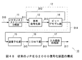
一方、図48は、JPEG2000規格に準拠した復号化装置10の構成を示すものである。   On the other hand, FIG. 48 shows a configuration of the decoding device 10 compliant with the JPEG2000 standard.

この復号化装置10においては、上述のようにして生成されたJPEG2000規格のシンタクスに合った符号化パケットデータD10から画像情報部分である符号化データD11を抽出し、これをEBCOTブロック12の算術復号化部13に送出する。   In this decoding apparatus 10, encoded data D 11 that is an image information part is extracted from encoded packet data D 10 that conforms to the syntax of the JPEG 2000 standard generated as described above, and this is subjected to arithmetic decoding of the EBCOT block 12. To the conversion unit 13.

算術復号化部13は、符号化データD11及び後段のビットデモデル部14から与えられるコンテクストデータD12を入力とした所定の算術復号化演算処理を実行し、かくして得られたシンボルデータD13をビットデモデル部14に送出する。   The arithmetic decoding unit 13 executes predetermined arithmetic decoding operation processing using the encoded data D11 and the context data D12 given from the bit demodeling unit 14 at the subsequent stage as inputs, and the symbol data D13 thus obtained is bit-decoded. The data is sent to the model unit 14.

ビットデモデル部14は、供給されるシンボルデータD13をCBM処理により係数ビットモデル化し、かくして得られた復号されたコードブロックデータD14を逆量子化部15に送出すると共に、このとき得られたコンタクスをコンタクスデータD12として算術復号化部13に送出する。   The bit demodeling unit 14 converts the supplied symbol data D13 into a coefficient bit model by CBM processing, sends the decoded code block data D14 thus obtained to the inverse quantization unit 15, and also obtains the syntax obtained at this time. Is sent to the arithmetic decoding unit 13 as the contact data D12.

逆量子化部15は、供給される復号量子化データD14に対して逆量子化処理を施すことによりウェーブレット係数を得、これを復号DWTデータD16としてIDWT部16に送出する。   The inverse quantization unit 15 obtains wavelet coefficients by performing inverse quantization processing on the supplied decoded quantized data D14, and sends this to the IDWT unit 16 as decoded DWT data D16.

IDWT部16は、供給される復号DWTデータD16に対してウェーブレット逆変換処理を施し、かくして得られたウェーブレット逆変換画像データD16を入力画像処理部17に送出する。   The IDWT unit 16 performs wavelet inverse transform processing on the supplied decoded DWT data D16 and sends the wavelet inversely transformed image data D16 thus obtained to the input image processing unit 17.

そして入力画像処理部17は、このウェーブレット逆変換画像データD16に対して所定の信号処理を施す。これにより符号化装置1(図46)において符号化された画像データD1(図46)を復号した画像データD17を得ることができる。   The input image processing unit 17 performs predetermined signal processing on the wavelet inversely transformed image data D16. Thereby, the image data D17 obtained by decoding the image data D1 (FIG. 46) encoded by the encoding device 1 (FIG. 46) can be obtained.

なお、JPEG2000規格に準拠した符号化装置及び復号化装置に関する文献としては、以下の特許文献1や非特許文献1がある。
特開2002−159009公報 特願2003−130793号
Note that there are the following Patent Document 1 and Non-Patent Document 1 as documents relating to an encoding device and a decoding device compliant with the JPEG2000 standard.
JP 2002-159209 A Japanese Patent Application No. 2003-130793

ところが、かかるJPEG2000規格による符号化処理及び復号化処理は、処理内容が煩雑で、高速化を図り難い問題があった。   However, the encoding process and the decoding process according to the JPEG2000 standard have a problem that the processing contents are complicated and it is difficult to increase the speed.

本発明は以上の点を考慮してなされたもので、符号化処理又は復号化処理を高速化させ得る符号化装置及び方法、復号化装置及び方法並びにプログラムを提案しようとするものである。   The present invention has been made in view of the above points, and an object of the present invention is to propose an encoding apparatus and method, a decoding apparatus and method, and a program capable of speeding up the encoding process or the decoding process.

かかる課題を解決するため本発明においては、コードブロックデータから形成されたビットプレーンのうち、上位の桁のビットプレーンから順に当該ビットプレーン上のビットを所定数でなるストライプに区切り、一のストライプに属するビットを読み出した後に次のストライプに属するビットを読み出すことにより処理対象となる処理ビットを所定の順序で読み出し、処理ビットの存在する処理ビットプレーンよりも上位となる上位プレーンにおいて1であるビットが存在する場合が有意であり、1であるビットが存在しない場合を有意でないとし当該上位プレーンにおける各ビットの有意性をSIGビットからなるSIGプレーンとして記憶する際、ストライプごとの処理ビットから少なくとも1ビットずらした単位ごとに所定数のSIGビットを記憶し、第1のメモリから単位ごとに供給されるSIGビットのうち、ストライプごとの処理ビットに対応するSIGビット、及び当該対応するSIGビットの上下に存在するSIGビットを保持し、SIGプレーンにおいて、処理ビットに対応するSIGビットが有意でなく、処理ビットに対応するSIGビットの周囲近傍に存在するSIG近傍ビットが有意である場合には、SIGプレーンを参照して当該処理ビットをモデル化する第1の処理を実行すると共に、当該処理ビットの値をSIGプレーンに反映させるようにした。 In order to solve such a problem, in the present invention, among the bit planes formed from the code block data, the bits on the bit plane are divided into a predetermined number of stripes in order from the bit digit of the upper digit to form one stripe. By reading out the bits belonging to the next stripe after reading out the bits belonging to them, the processing bits to be processed are read out in a predetermined order, and a bit which is 1 in the upper plane higher than the processing bit plane in which the processing bits exist is It is significant if it exists, and it is not significant if there is no 1 bit, and when storing the significance of each bit in the upper plane as a SIG plane consisting of SIG bits, at least one bit from the processing bits for each stripe Predetermined number of SI for each shifted unit Stores SIG bits corresponding to the processing bits for each stripe, and SIG bits that exist above and below the corresponding SIG bits, among the SIG bits supplied from the first memory for each unit. In the plane, when the SIG bit corresponding to the processing bit is not significant and the SIG neighboring bits existing around the SIG bit corresponding to the processing bit are significant, the processing bit is modeled with reference to the SIG plane. The first processing is executed, and the value of the processing bit is reflected on the SIG plane.

この結果本発明によれば、記憶手段にアクセスする回数を格段的に低減させることができる。 The results show the present invention, it is possible to dramatically reduce the number of accesses to memorize means.

また本発明においては、所定の画素数でなる画像データにおける各画素を所定の桁数のビットで表すことにより形成されたコードブロックデータから桁ごとに平面化されてなるビットプレーンを生成するために、ビットとして供給されるシンボルデータのうち処理対象となる処理ビットを所定数ごとに読み出し、処理ビットの存在する処理ビットプレーンよりも上位となる上位プレーンにおいて1であるビットが存在する場合が有意であり、1であるビットが存在しない場合を有意でないとし当該上位プレーンにおける各ビットの有意性をSIGビットからなるSIGプレーンとして記憶する際、ストライプごとの処理ビットから少なくとも1ビットずらした単位ごとに所定数のSIGビットを記憶し、第1のメモリから単位ごとに供給されるSIGビットのうち、ビットプレーン上のビットが所定数ごとに区切られてなるストライプごとの処理ビットに対応するSIGビット、及び当該対応するSIGビットの上下に存在するSIGビットを保持し、SIGプレーンにおいて、処理ビットに対応するSIGビットが有意でなく、処理ビットに対応するSIGビットの周囲近傍に存在するSIG近傍ビットが有意である場合には、SIGプレーンを参照して当該処理ビットをモデル化する第1の処理を実行すると共に、当該処理ビットの値をSIGプレーンに反映させるようにした。 In the present invention, in order to generate a bit plane that is flattened for each digit from the code block data formed by representing each pixel in the image data having a predetermined number of pixels by a predetermined number of bits. It is significant that a predetermined number of processing bits to be processed are read out from the symbol data supplied as bits, and there is a bit that is 1 in an upper plane that is higher than the processing bit plane in which the processing bits exist. Yes, when the bit that is 1 is not significant, the significance of each bit in the upper plane is stored as a SIG plane made up of SIG bits, and predetermined for each unit shifted by at least one bit from the processing bit for each stripe. Stores a number of SIG bits and is supplied per unit from the first memory Among the SIG bits, the SIG bits corresponding to the processing bits for each stripe in which the bits on the bit plane are divided by a predetermined number, and the SIG bits existing above and below the corresponding SIG bits are held. If the SIG bit corresponding to the processing bit is not significant and the SIG neighboring bits existing in the vicinity of the SIG bit corresponding to the processing bit are significant, the processing bit is modeled with reference to the SIG plane. While executing the first processing, the value of the processing bit is reflected in the SIG plane.

この結果本発明によれば、記憶手段にアクセスする回数を格段的に低減させることができる。 The results show the present invention, it is possible to dramatically reduce the number of accesses to memorize means.

発明によれば、記憶手段にアクセスする回数を格段的に低減させることができ、処理を高速化し得る画像処理装置、画像処理方法及び画像処理プログラムを実現できる。 According to the present invention, serial Ki times the of dramatically out to reduce access to憶means, an image processing apparatus capable of speeding up the processing can be realized an image processing method and image processing program.

以下図面について、本発明の一実施の形態を詳述する。   Hereinafter, an embodiment of the present invention will be described in detail with reference to the drawings.

(1)CBM処理の内容
本願発明は上述したJPEG2000規格に準拠した符号化装置1のビットモデル部6(図46)や復号化装置10のビットデモデル部13(図48)において行われるCBM処理に関するものである。そこで、まずCBM処理の具体的処理内容について詳説する。
(1) Contents of CBM processing The present invention relates to CBM processing performed in the bit model unit 6 (FIG. 46) of the encoding device 1 and the bit demodeling unit 13 (FIG. 48) of the decoding device 10 compliant with the above-described JPEG2000 standard. It is about. First, the specific processing contents of the CBM processing will be described in detail.

(1−1)1コードブロックとコードブロックサイズ
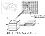
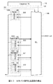
図46について上述したように、例えばJPEG2000規格に準拠した符号化装置1の量子化部4では、ウェーブレット係数を量子化したものをコードブロックと呼ばれる単位で切り出してビットモデル部6に与える。そしてビットモデル部6では、図1に示すように、このコードブロック20を単位としてCBM処理を行い、シンボルとコンテクストを生成することになる。
(1-1) 1 Code Block and Code Block Size As described above with reference to FIG. 46, for example, in the quantization unit 4 of the encoding device 1 compliant with the JPEG2000 standard, a unit obtained by quantizing wavelet coefficients is called a code block. And is supplied to the bit model unit 6. As shown in FIG. 1, the bit model unit 6 performs CBM processing in units of the code block 20 to generate symbols and contexts.

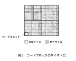
ここでコードブロック20のサイズは、図2に示すように、大枠が定められている。従って、コードブロック20のサイズは、エンコード時にこのルールに従って選択することになる。   Here, the size of the code block 20 is roughly defined as shown in FIG. Therefore, the size of the code block 20 is selected according to this rule at the time of encoding.

この場合、コードブロック20は基本的にはサブバンドの左上境界から始まって位置付けられるので、図3に示すように、画像サイズとコードブロックサイズとの関係によっては不整合を生じる。このようにエンコード時に決定したものを通常サイズと呼び、不整合が生じたものを例外サイズと呼ぶ。   In this case, since the code block 20 is basically positioned starting from the upper left boundary of the subband, as shown in FIG. 3, inconsistency occurs depending on the relationship between the image size and the code block size. In this way, what is determined at the time of encoding is called a normal size, and what is inconsistent is called an exception size.

例外サイズは必ず通常サイズよりも小さいものであり、基本的に格納しているデータの量が異なるだけであるので、例外サイズについて触れるのはここだけに留め、以下においては通常サイズのコードブロック20を取り上げて説明する。   Since the exception size is always smaller than the normal size and basically the amount of data stored is different, only the exception size is mentioned here, and in the following, the normal size code block 20 Will be explained.

(1−2)ビットプレーン
上述のように、CBM処理ではコードブロック20を単位として処理(モデル化、シンボル・コンテクスト出力)を行うわけであるが、この処理はコードブロック20のデータをビットプレーンに分けて順に行われる。ビットプレーンはその名のとおり、『bit(0/1)』を表現するものが集まった平面である。
(1-2) Bit Plane As described above, in the CBM processing, processing (modeling, symbol context output) is performed in units of the code block 20, but this processing converts the data of the code block 20 into a bit plane. Divided in order. As its name suggests, the bit plane is a plane in which things representing “bit (0/1)” are gathered.

図4に示すように、コードブロック20に分割されてきたデータは『Sign-Magnitude表現』、すなわち正負符号と絶対値による数値表現により表されている。最上位のビットプレーン22に各画素の正負符号が格納され、これを正負符号ビットプレーン22Sと呼ぶ。そしてこれよりも下位のビットプレーン22に各画素の絶対値データがビットごとに順に格納される。   As shown in FIG. 4, the data divided into the code blocks 20 is represented by “Sign-Magnitude expression”, that is, numerical expression by a positive / negative sign and an absolute value. The sign of each pixel is stored in the most significant bit plane 22, and this is called the sign bit plane 22S. Then, the absolute value data of each pixel is sequentially stored for each bit in the lower bit plane 22.

ここで仮に各画素のデータが16ビットで表現されているとすると、コードブロックデータ20は、各画素の最上位ビット(bit15)が集まって構成するプレーンから最下位ビット(bit0)が集まって構成するプレーンまでの16枚のビットプレーン22に分割されることになる。   Assuming that the data of each pixel is expressed by 16 bits, the code block data 20 is configured by collecting the least significant bit (bit 0) from the plane formed by collecting the most significant bit (bit 15) of each pixel. It is divided into 16 bit planes 22 up to the plane to be processed.

上位のビットプレーン22から順に眺めていくと、上述のように最上位ビットが集まって構成するビットプレーン22が正負符号ビットプレーン22Sであり、各画素の正負符号が格納される。   When viewed from the upper bit plane 22 in order, the bit plane 22 constituted by the most significant bits gathering as described above is the plus / minus sign bit plane 22S, and stores the sign of each pixel.

各画素のその次のビットが集まって構成するビットプレーン22から最下位ビットが集まって構成するビットプレーン22までの合計15枚の各ビットプレーン22に、各画素のデータの絶対値がビットごとに分割されて格納されていることになる。この場合、統計的に上位のいくつかのビットプレーン22では全てのビット値が0であるということが多い。このようなものをゼロビットプレーン220と呼ぶ。   The absolute value of the data of each pixel is set for each bit in a total of 15 bit planes 22 from the bit plane 22 composed of the next bit of each pixel to the bit plane 22 composed of the least significant bit. It is divided and stored. In this case, all the bit values are often 0 in some statistically higher bit planes 22. Such a thing is called a zero bit plane 220.

かかる15枚のビットプレーン22を上から順に見ていくと、やがて初めてゼロビットプレーン220ではないビットプレーン22にたどりつく。それをトップビットプレーン22Tと呼び、ここではそれが各画素の最下位ビット(bit0)から数えて10番目のビット(bit9)が集まって構成しているビットプレーン22だったとする。これよりも下位のビットプレーン22(それぞれ各画素の9番目以下のビットが集まって構成される各ビットプレーン22)は、データがあったり無かったりしてもここでは特に分類はしない。   When the 15 bit planes 22 are viewed in order from the top, the bit plane 22 that is not the zero bit plane 220 is reached for the first time. This is referred to as a top bit plane 22T, and here it is assumed that it is a bit plane 22 composed of the tenth bit (bit 9) counted from the least significant bit (bit 0) of each pixel. The lower-order bit planes 22 (each bit plane 22 formed by collecting the ninth and lower bits of each pixel) are not particularly classified here even if there is data.

ここまでの話しをまとめると、この例では、各画素の最上位ビット(bit15)が集まって構成しているものが正負符号ビットプレーン22S、各画素の次のビット(bit14)が集まって構成しているビットプレーン22から11番目のビット(bit10)が集まって構成しているビットプレーン22がゼロビットプレーン220(10枚)、10番目のビット(bit9)が集まって構成しているビットプレーン22がトップビットプレーン22T、9番目(bit8)のビットが集まって構成しているビットプレーン22から最下位ビットが集まって構成しているビットプレーン22までが残りの処理すべきビットプレーン22(9枚)というビットプレーン構成となっている。   To sum up the discussion so far, in this example, the most significant bit (bit 15) of each pixel is composed of the sign bit plane 22S and the next bit (bit 14) of each pixel is composed. The bit plane 22 formed by collecting the eleventh bit (bit 10) from the bit planes 22 formed by the zero bit plane 220 (10) and the bit plane 22 formed by collecting the tenth bit (bit 9). Is the top bit plane 22T, the bit plane 22 composed of the ninth (bit8) bits and the bit plane 22 composed of the least significant bits, the remaining bit planes to be processed (9) ) Bit plane configuration.

このようなビットプレーン構成のコードブロック20に対し、上述のビットモデル部6(図46)やビットデモデル部13(図48)では次のようにCBM処理を行う。
1. 符号ビットプレーン22Sに対する処理は、後回しにする。
2. ゼロビットプレーン220に対してはCBM処理を行わない。
3. トップビットプレーン22Tで初めてCBM処理を行う。このCBM処理は“Clean-up Pass”(以下、これをCUパスと呼ぶ)と呼ばれる。
4. 残りの処理すべきビットプレーン22に対し、上位のビットプレーン22から順に、“Significance Propagation Pass”(以下、これをSPパスと呼ぶ)、“Magnitude
Refinement Pass”(以下、これをMRパスと呼ぶ)及びCUパスをビットプレーン22ごとにそれぞれ行う。
The bit model unit 6 (FIG. 46) and the bit demodel unit 13 (FIG. 48) perform CBM processing on the code block 20 having such a bit plane configuration as follows.
1. The processing for the sign bit plane 22S is postponed.
2. CBM processing is not performed for the zero bit plane 220.
3. Perform CBM processing for the first time on the top bit plane 22T. This CBM processing is called “Clean-up Pass” (hereinafter referred to as CU pass).
4. With respect to the remaining bit planes 22 to be processed, in order from the higher-order bit plane 22, "Significance Propagation Pass" (hereinafter referred to as an SP path), "Magnitude"
Refinement Pass ”(hereinafter referred to as MR pass) and CU pass are performed for each bit plane 22.

なお、SPパス、MRパス及びCUパスの詳細については後述する。   Details of the SP path, MR path, and CU path will be described later.

(1−3)ビットプレーン内スキャン順序
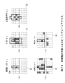
コードブロック20内の各ビットプレーン22に対するアクセス順序はこれまでに説明した通りであるが、ビットプレーン22内において、各画素のデータにどういう順序でアクセスするかを示したのが図5である。この図5では、ビットプレーン22として8画素×8画素のものを例示している。
(1-3) Scan Order within Bit Plane The access order for each bit plane 22 in the code block 20 is as described above, but in what order the data of each pixel is accessed in the bit plane 22. This is shown in FIG. In FIG. 5, the bit plane 22 is exemplified by 8 pixels × 8 pixels.

ビットプレーン22は、縦4画素ずつ横方向に区切った場合の各行であるストライプ23に分けられる。ストライプ23中の縦1列をストライプカラム23Aと呼ぶ。ビットプレーン22の最上段のストライプ23における左端のストライプカラム23Aから処理を始め、1つのストライプカラム23Aを処理したら隣のストライプカラム23Aに移り、それをそのストライプ23中繰り返す。1ストライプ23の処理が完了したら下段のストライプ23に移動し、ビットプレーン22内の全ての画素を処理し終えるまでこれを繰り返すというのがビットプレーン22内でのスキャン順序(以下、これをビットプレーン内スキャン順序と呼ぶ)である。   The bit plane 22 is divided into stripes 23, which are each row when the pixel is divided horizontally by 4 pixels. One vertical column in the stripe 23 is called a stripe column 23A. The processing starts from the leftmost stripe column 23 A in the uppermost stripe 23 of the bit plane 22, and when one stripe column 23 A is processed, the processing proceeds to the adjacent stripe column 23 A and is repeated in the stripe 23. When the processing of one stripe 23 is completed, the process moves to the lower stripe 23 and repeats until all the pixels in the bit plane 22 have been processed. This is called the inner scan order).

さらに、ビットプレーン22内におけるスキャンと3つのパス(SPパス、MRパス及びCUパス)との関係について以下に説明する。   Further, the relationship between the scan in the bit plane 22 and three paths (SP path, MR path, and CU path) will be described below.

上述のようにトップビットプレーン22Tに対してCUパスのみを行い、それよりも下位のビットプレーン22に対しては、SPパス、MRパス及びCUパスの3つのパスを処理する。これとビットプレーン22内におけるスキャンとの関係を図6〜図9に示す。   As described above, only the CU pass is performed on the top bit plane 22T, and the lower-order bit plane 22 is processed with the three passes of the SP pass, the MR pass, and the CU pass. The relationship between this and the scan in the bit plane 22 is shown in FIGS.

まず新たにビットプレーン22をCBM処理しようという場合において、まだひとつのデータも処理されておらずこれから処理を開始しようとしている状態が図6である。SPパスの処理が必要な画素に対して行われ、このSPパス処理の終了した状態が図7となる。SPパスはビットプレーン内スキャン順序を守って行われる。   First, when a new bit plane 22 is to be subjected to CBM processing, FIG. 6 shows a state in which one piece of data has not yet been processed and processing is about to start. FIG. 7 shows a state in which the SP pass processing is performed on the pixels that require the SP pass processing and the SP pass processing is completed. The SP pass is performed in accordance with the scan order in the bit plane.

次のMRパスは、SPパスで処理した画素は避け、該当する画素に対してのみ処理を行う。このMRパスの終了した状態が図8である。このMRパスにおいてもビットプレーン内スキャン順序は守る。   The next MR pass avoids the pixels processed in the SP pass and performs the processing only on the corresponding pixels. FIG. 8 shows a state in which this MR pass is completed. Even in this MR pass, the scan order in the bit plane is maintained.

さらに未処理で残った画素に対してもやはりビットプレーン内スキャン順序を守りながらCUパスで処理を行う。このCUパスの完了した状態が図9である。この結果、すべての画素が処理済みになったので、このビットプレーン22のビットモデル化は完了したことになる。   Further, the remaining pixels that have not been processed are also processed by the CU pass while keeping the scan order in the bit plane. FIG. 9 shows the completed state of this CU pass. As a result, since all the pixels have been processed, the bit modeling of the bit plane 22 has been completed.

なお『トップビットプレーン22T』については、CUパスの処理のみを全ての画素に対して行う。   For the “top bit plane 22T”, only the CU pass processing is performed for all pixels.

(1−4)“Significance”について
次に各コーディング・パス(SPパス、MRパス及びCUパス)の説明に入る前に、“Significance”という状態量について説明する。“Significance”とは該当画素が『有意である(Significant)/有意でない(Insignificant)』ということを意味する。
(1-4) About “Significance” Next, before describing each coding pass (SP pass, MR pass, and CU pass), a state quantity “Significance” will be explained. “Significance” means that the corresponding pixel is “significant / insignificant”.

『有意である(Significant)』とは、「これまでのCBM処理によって該当画素が0ではないとわかっている状態」のことをいい、換言すれば「値が『1』である画素(ビット)をすでにモデル化(符号化)し終えた」ということを意味する。   “Significant” means “a state in which the corresponding pixel is known not to be 0 by the conventional CBM processing”, in other words, “a pixel (bit) whose value is“ 1 ””. Has already been modeled (encoded).

また『有意でない(Insignificant)』とは、「該当画素の画素値が0であるか、又は0の可能性がある状態」のことをいい、換言すれば「(今のところ)値が『1』である画素(ビット)を未だモデル化(符号化)し終えていない」ということを意味する。   “Insignificant” means “a state in which the pixel value of the corresponding pixel is 0 or possibly 0”, in other words, the value “(for now) is“ 1 ”. ”Has not yet been modeled (encoded).

さらに『該当画素』とは、ビットプレーン22上のある着目している画素のことをいう。   Further, “corresponding pixel” refers to a pixel of interest on the bit plane 22.

なお、“Significance”はコードブロック20(図1)の全体に渡って更新されながら記憶保持される。従ってこれまで例示した8画素×8画素のビットプレーン22が16枚からなるコードブロック20においていえば、64画素(8画素×8画素)分の“Significance”状態量をコードブロック20に渡って記憶保持することになる。   “Significance” is stored and held while being updated throughout the entire code block 20 (FIG. 1). Accordingly, in the code block 20 having 16 bit planes 22 of 8 pixels × 8 pixels exemplified so far, the “Significance” state quantity for 64 pixels (8 pixels × 8 pixels) is stored across the code block 20. Will hold.

CBM処理では、時間的にトップビットプレーン22Tから順に、ビットプレーン22内ではビットプレーン内スキャン順序に従って3つのコーディング・パス(トップビットプレーン22TではCUパスのみ)を処理(モデル化、シンボル・コンテクスト出力)するが、ある画素の係数(正確にはウェーブレット変換係数を量子化したもの)の状態をこの“Significance”で表していることになる。   In the CBM processing, three coding passes (only the CU pass for the top bit plane 22T) are processed (modeled, symbol context output) in order from the top bit plane 22T in time and in the bit plane 22 according to the scan order in the bit plane. However, the state of the coefficient of a certain pixel (more precisely, the quantized wavelet transform coefficient) is represented by this “Significance”.

因みに、CBM処理が行われていないコードブロック20においては、すべてのSIGプレーン上の値が“Insignificant”で始まり、各ビットプレーン22を処理していく過程において該当するものが“Significant”に転じていく。一度“Significant”になったものがCBM処理の途中で“Insignificant”に戻ることはない。   Incidentally, in the code block 20 in which CBM processing is not performed, the values on all SIG planes start with “Insignificant”, and the corresponding ones in the process of processing each bit plane 22 change to “Significant”. Go. What once becomes “Significant” does not return to “Insignificant” during the CBM process.

(1−5)3つのコーディング・パス
次に、SLパス(Significance Propagation Pass)、MRパス(Magnitude Refinement Pass )、CUパス(Clean−up Pass)について説明する。
(1-5) Three Coding Paths Next, an SL path (Significance Propagation Pass), an MR path (Magnitude Refinment Pass), and a CU path (Clean-up Pass) will be described.

この3つのコーディング・パスに従ってビットモデル化の処理を行う場合には、図10に示すように、これから処理しようとするビットプレーン22(以下、これを処理ビットプレーン22と呼ぶ)以外に、正負符号ビットプレーン22S(図4)のデータを記憶保持するプレーン(以下、これを正負符号プレーンと呼ぶ)30と、“Significance”を記録するプレーン(以下、これをSIGプレーンと呼ぶ31)と、最初の“Refinement pass”であるか否か示すプレーン(以下、これをREFプレーンと呼ぶ)32と、処理ビットプレーン中で着目ビットが処理済みであるか否かを表すプレーン(以下、これをDONEプレーンと呼ぶ)33とを状態量の記録用RAMとして用意するのが一般的である。   When performing the bit modeling process according to these three coding passes, as shown in FIG. 10, in addition to the bit plane 22 to be processed (hereinafter referred to as the processing bit plane 22), the sign A plane for storing and holding data of the bit plane 22S (FIG. 4) (hereinafter referred to as “positive / negative sign plane”) 30, a plane for recording “Significance” (hereinafter referred to as SIG plane 31), A plane (hereinafter referred to as a REF plane) 32 indicating whether or not it is a “Refinement pass”, and a plane (hereinafter referred to as a DONE plane) indicating whether or not the target bit has been processed in the processing bit plane. 33) is generally prepared as a state quantity recording RAM.

これら正負符号プレーン30、SIGプレーン31、REFプレーン32及びDONEプレーン33は、処理ビットプレーン22と同じ大きさを持つ(これまでの例では8画素×8画素)プレーンである。   The positive / negative code plane 30, the SIG plane 31, the REF plane 32, and the DONE plane 33 are planes having the same size as the processing bit plane 22 (8 pixels × 8 pixels in the examples so far).

この場合、正負符号プレーン30は、コードブロック22を処理している間はその値が変化せず記憶保持される。SIGプレーン31は、SPパス、CUパスで値を変化させられる可能性がある。REFプレーン32は、MRパスで値を変化させられる可能性がある。DONEプレーン33は、各コーディング・パスの処理が完了した画素に対応させて処理済のフラグを立てる状態量で、その処理ビットプレーン22に対する処理が完了した段階でリセットされる。   In this case, the value of the positive / negative sign plane 30 is stored and held without changing its value while the code block 22 is processed. The SIG plane 31 may be changed in value by the SP path and the CU path. The REF plane 32 may be changed in value by the MR path. The DONE plane 33 is a state quantity that sets a processed flag corresponding to a pixel for which the processing of each coding pass has been completed, and is reset when the processing for the processing bit plane 22 is completed.

(1−5−1)SPパスの処理
SPパスは、トップビットプレーン22T(図4)を除く処理ビットプレーン22において、最初に実施されるコーディング・パスである。このSPパスは、処理ビットプレーン22上の該当画素と同じ座標位置にあるSIGプレーン31上のデータを参照しながら処理が進められる。
(1-5-1) SP Pass Processing The SP pass is a coding pass that is first performed in the processing bit plane 22 except for the top bit plane 22T (FIG. 4). This SP pass is processed while referring to data on the SIG plane 31 at the same coordinate position as the corresponding pixel on the processing bit plane 22.

すなわち図11に示すように、例えば処理ビットプレーン22上における該当画素の座標が(2,1)であったとき(図11(B))、SIGプレーン31上のこの該当画素に対応するビット(図11(C)における座標(2,1)のビット)と、その8近傍のビットとを合わせた(1,0)、(2,0)、(3,0)、(1,1)、(2,1)、(3,1)、(1,2)、(2,2)、(3,2)の各座標位置のデータを参照することになる。なお参照する8近傍のビットうち、処理ビットプレーン22の外側に位置してしまったビットはすべて“Insignificant”とされる。   That is, as shown in FIG. 11, for example, when the coordinates of the corresponding pixel on the processing bit plane 22 are (2, 1) (FIG. 11B), the bit corresponding to the corresponding pixel on the SIG plane 31 ( (1, 0), (2, 0), (3, 0), (1, 1), which is obtained by combining the bits of the coordinates (2, 1) in FIG. The data of each coordinate position of (2, 1), (3, 1), (1, 2), (2, 2), (3, 2) will be referred to. Of the 8 neighboring bits to be referred to, all the bits positioned outside the processing bit plane 22 are set to “Insignificant”.

SPパスの処理を行うに際しては、上述したビットプレーン内スキャン順序に従って、処理ビットプレーン22の左上を起点に、当該処理ビットプレーン22上の画素ごとに当該処理を行うことができるかどうかを調べる。具体的には、「『該当画素が“Significant”ではない(Insignificant)』かつ『該当画素の8近傍に“Significant”である画素が少なくともひとつ存在する』」という条件を満たすか否かを調査する。   When performing the SP pass processing, it is checked whether the processing can be performed for each pixel on the processing bit plane 22 starting from the upper left of the processing bit plane 22 according to the above-described intra-bit-plane scan order. Specifically, it is investigated whether or not the condition ““ the relevant pixel is not “Significant” ”and“ there is at least one pixel that is “Significant” in the vicinity of 8 ”” is satisfied. .

そしてこの条件を満たすときにその該当画素に対してSPパス
の処理を行い、満たさないときにはSPパスの処理を行わずにビットプレーン内スキャン順序に従って次の画素を評価する。
When this condition is satisfied, SP pass processing is performed on the corresponding pixel, and when not satisfied, SP pass processing is not performed, and the next pixel is evaluated according to the scan order in the bit plane.

次に、SPパスの処理に入った場合の流れを説明する。   Next, the flow when entering the SP pass process will be described.

SPパスに入った場合、シンボルとして図12(A)に示す処理ビットプレーン22の該当画素の値(0/1)を出力する。同時に、処理ビットプレーン22上の該当画素と対応する図12(B)に示すSIGプレーン31上のビットを囲む8近傍のビットのうち、“Significant”であるビットの数を数え、図13に示すルールに従ってコンテクストを出力する。   When the SP pass is entered, the value (0/1) of the corresponding pixel of the processing bit plane 22 shown in FIG. 12A is output as a symbol. At the same time, among the 8 neighboring bits surrounding the bit on the SIG plane 31 shown in FIG. 12B corresponding to the corresponding pixel on the processing bit plane 22, the number of “Significant” bits is counted and shown in FIG. Output context according to rules.

なおこの図13において、『ΣH』、『ΣV』、『ΣD』及び『ΣH+ΣV』は、それぞれ処理ビットプレーン22上の該当画素と対応するSIGプレーン31上のビットの8近傍における左右2つのビット、上下2つのビット、斜め4つのビット、又は上下左右4つのビットうちの“Significant”であるビットの合計値を表す。   In FIG. 13, “ΣH”, “ΣV”, “ΣD”, and “ΣH + ΣV” are two left and right bits in the vicinity of 8 bits on the SIG plane 31 corresponding to the corresponding pixel on the processing bit plane 22, respectively. It represents the total value of “Significant” bits among the two upper and lower bits, the four diagonal bits, or the upper, lower, left and right four bits.

また『CX』は、そのような状態のときのコンテクストを表す。例えば、その処理ビットプレーン22を含むコードブロック20(図1)が画像のLL成分(図47)であり、このとき『ΣH』、『ΣV』及び『ΣD』がそれぞれ0、0及び1であった場合のコンテクストは1となり、『ΣH』、『ΣV』及び『ΣD』がそれぞれ1、0及び0であった場合のコンテクストは5となる。   “CX” represents the context in such a state. For example, the code block 20 (FIG. 1) including the processing bit plane 22 is the LL component (FIG. 47) of the image, and at this time, “ΣH”, “ΣV”, and “ΣD” are 0, 0, and 1, respectively. The context is 1 and “ΣH”, “ΣV” and “ΣD” are 1, 0 and 0, respectively, and the context is 5.

シンボルの値が0である場合は、その該当画素に対するSPパスの処理がこれで完了し、この該当画素とDONEプレーン33(図10)上の同じ座標位置にビットモデル化が完了した旨のフラグを立てる。   When the value of the symbol is 0, the SP pass processing for the corresponding pixel is completed, and a flag indicating that bit modeling is completed at the same coordinate position on the corresponding pixel and the DONE plane 33 (FIG. 10). Stand up.

これに対してシンボルの値が1(すなわち該当画素の値が1)だった場合は、この該当画素は初めて1が現れた画素であることになり、いままで“Insignificant”であったが、ここで初めて“Significant”に転じ、SIGプレーン31上の同じ座標位置にフラグを立てる。このときREFプレーン32(図10)上の同座標位置にもフラグを立てる。これは次のMRパスのための処理である。   On the other hand, if the value of the symbol is 1 (that is, the value of the corresponding pixel is 1), this corresponding pixel is the pixel in which 1 appears for the first time, and it has been “Insignificant” until now. Then, for the first time, “Significant” is set and a flag is set at the same coordinate position on the SIG plane 31. At this time, a flag is also set at the same coordinate position on the REF plane 32 (FIG. 10). This is processing for the next MR pass.

さらに、その該当画素と同じ座標位置にある正負符号プレーン30上のビット(すなわち該当画素に対応する正負符号)の上下左右4近傍のビットを参照し、図14に示すルールに従ってコンテクストを出力する。   Furthermore, referring to the bits near the top, bottom, left, and right of the bit on the positive / negative sign plane 30 at the same coordinate position as the corresponding pixel (that is, the positive / negative sign corresponding to the corresponding pixel), the context is output according to the rule shown in FIG.

またこれと同時にXOR信号も出力され、これと当該コンテクストの排他的論理和を取ったものを、正負符号のシンボルとして出力することにより該当画素に対応する正負符号のビットモデル化を完了し、この段階でこの該当画素についてのSPパスの処理も完了となる。このときDONEプレーン33(図10)上の該当画素と同じ座標位置にビットモデル化が完了したことを表すフラグを立てる。   At the same time, an XOR signal is also output, and an exclusive OR of this and the context is output as a symbol with a positive / negative sign, thereby completing bit modeling of the positive / negative sign corresponding to the corresponding pixel. At this stage, the SP pass processing for the corresponding pixel is also completed. At this time, a flag indicating that the bit modeling is completed is set at the same coordinate position as the corresponding pixel on the DONE plane 33 (FIG. 10).

なお、上述のことからも明らかなように、スキャン順序によっては、SPパスによって“Significant”に新たに転じたものが他の(近傍)画素のSIGプレーン31上の8近傍参照時に影響を与えることがある。   As is clear from the above, depending on the scan order, what is newly changed to “Significant” by the SP pass may affect the reference of 8 neighbors on the
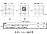
 SIG plane 31 of other (neighboring) pixels. There is.

(1−5−2)MRパスの処理
MRパスは、トップビットプレーン22T(図4)を除く処理ビットプレーン22について、SPパスに続いて実施されるコーディング・パスである。図15に処理の概略を示す。
(1-5-2) MR Pass Processing The MR pass is a coding pass that is performed following the SP pass for the processing bit planes 22 excluding the top bit plane 22T (FIG. 4). FIG. 15 shows an outline of the processing.

このMRパスの処理を行うに際しては、上述したビットプレーン内スキャン順序に従って、処理ビットプレーン22の左上を起点に、当該処理を行うことができるかどうかを各画素について調べる。具体的には、「『未処理(DONEプレーン33上の該当画素と同じ座標位置にフラグが立っていない)の処理ビットプレーン22上の該当画素』であって『その該当画素が“Significant”である』」という条件を満たすか否かを調査する。   When performing this MR pass processing, each pixel is examined to determine whether or not the processing can be performed starting from the upper left of the processing bit plane 22 in accordance with the above-described intra-bit-plane scan order. Specifically, ““ the corresponding pixel on the processing bit plane 22 that has not been processed (the flag is not set at the same coordinate position as the corresponding pixel on the DONE plane 33) ”and“ the corresponding pixel is “Significant” Investigate whether or not the condition “Yes” is met.

そしてこの条件を満たすときにその該当画素に対してMRパスの処理を行い、満たさないときにはMRパスの処理を行わずに上述のビットプレーン内スキャン順序に従って処理ビットプレーン22上の次の画素を評価する。   When this condition is satisfied, MR pass processing is performed on the corresponding pixel, and when not satisfied, MR pass processing is not performed, and the next pixel on the processing bit plane 22 is evaluated according to the scan order within the bit plane. To do.

そしてMRパスの処理に入った場合、該当画素とSIGプレーン31上の同じ座標位置にあるビットの8近傍のビットを参照し、図16に示すルールに従ってコンテクストを出力し、同時に該当画素の値(0/1)をシンボル(図16において『X』)として出力する。   Then, when the MR pass processing is started, the corresponding pixel and 8 bits near the bit at the same coordinate position on the SIG plane 31 are referred to, and a context is output according to the rule shown in FIG. 0/1) is output as a symbol (“X” in FIG. 16).

図16において、『該当画素を最初に本パス(MRパス)で符号化』しているのかどうかという状態は、REFプレーン32(図10)の該当画素と同じ座標位置のフラグを参照する。このフラグが立っていれば、その該当画素が、SPパスで処理が行われた直後の処理ビットプレーン22上の画素であるということがわかる。ただし、これ以降の下位のビットプレーン22の処理時に誤って参照しないように、参照後にこのフラグをクリアする。   In FIG. 16, the state of whether or not “the relevant pixel is first encoded in this pass (MR pass)” refers to the flag at the same coordinate position as the relevant pixel of the REF plane 32 (FIG. 10). If this flag is set, it can be understood that the corresponding pixel is a pixel on the processing bit plane 22 immediately after the processing is performed in the SP pass. However, this flag is cleared after the reference so that it is not erroneously referred to when processing the lower bit plane 22 thereafter.

(1−5−3)CUパスの処理
トップビットプレーン22Tに対しては唯一これのみ、トップビットプレーン22Tを除く他の処理対象のビットプレーン22に対しては最後に実施されるコーディング・パスである。
(1-5-3) Processing of CU path This is the only coding path for the top bit plane 22T, and the coding path performed last for the bit planes 22 other than the top bit plane 22T. is there.

CUパスでは、上述したビットプレーン内スキャン順序に従って、処理ビットプレーン22の左上を起点に、CUパスの処理を行うことができるかどうかを各画素について調べるが、この段階で「未処理(DONEプレーン33上で該当画素と同じ座標位置にフラグが立っていない)の処理ビットプレーン22上の画素」、すなわち処理ビットプレーン22上のSPパス及びMRパスの処理対象とならない残りの画素がすべてCUパスの処理対象となる。   In the CU pass, each pixel is examined to determine whether or not the CU pass process can be performed starting from the upper left of the processing bit plane 22 in accordance with the above-described scan order within the bit plane. At this stage, the “unprocessed (DONE plane) The pixel on the processing bit plane 22 is not flagged at the same coordinate position as the corresponding pixel on 33 ”, that is, all the remaining pixels not subject to the processing of the SP pass and MR pass on the processing bit plane 22 are CU passes. It becomes a processing target.

CUパスでは、図17に示すように、上述したSPパスやMRパスのように該当画素と同じ座標位置にあるSIGプレーン31上のビットの8近傍の値を参照するものに加えて、もう少し大きいランレングス符号化を行う。   In the CU pass, as shown in FIG. 17, in addition to the above-mentioned SP pass and MR pass, in addition to the reference to the value in the vicinity of 8 bits on the SIG plane 31 at the same coordinate position as the corresponding pixel, it is a little larger. Run-length encoding is performed.

CUパスの処理は、まず処理ビットプレーン22の左上を起点に、ランレングス処理を行うことができるかどうかを調べる。具体的には、ストライプカラム23A単位で、「『当該ストライプカラム23A内の4画素すべてがCUパスで処理すべき画素である』かつ『当該ストライプカラム23A内の4画素すべてが“Insignificant”である』かつ『当該ストライプカラム23A内の4画素とそれぞれ同じ座標位置にあるSIGプレーン31上の4つのビットの各8近傍に“Significance”が存在しない』」という条件を満たすか否かを調査する。   In the processing of the CU path, first, it is checked whether or not run length processing can be performed starting from the upper left of the processing bit plane 22. Specifically, in the unit of the stripe column 23A, ““ all four pixels in the stripe column 23A are pixels to be processed by the CU pass ”and“ all four pixels in the stripe column 23A are “Insignificant”. And “there is no“ Significance ”in the vicinity of each of the eight bits of the four bits on the SIG plane 31 at the same coordinate position as the four pixels in the stripe column 23A” ”.

そしてこの条件を満たすときにランレングス処理に入り、コンテクストとして“run”を出力する。その上で、『当該ストライプカラム23A内の4画素の値がすべて0である』ときにはシンボルとして0を出力し、これに対して『当該ストライプカラム23Aの4画素の値がすべて0ではない』とき、すなわち4画素の中にひとつでも1が存在する場合には、(“run”を出力した上で)シンボルとして1を出力し、それに引き続いて2回“uniform”というコンテクストと対応するシンボルを出力する。   Then, when this condition is satisfied, the run length processing is entered and “run” is output as the context. In addition, when “the values of the four pixels in the stripe column 23A are all 0”, 0 is output as a symbol, and when “the values of the four pixels of the stripe column 23A are not all 0” In other words, if at least one 1 is present in 4 pixels, 1 is output as a symbol (after outputting “run”), and then a symbol corresponding to the context “uniform” is output twice. To do.

この際“uniform”コンテクストに対応するシンボルは、図18に示すようなルールでエンコードを行う。この図18で説明すると、ストライプカラム23A内の4画素が上から順に0、0、1、0で、初めて1が出てきたその位置を表現する『1、0』なる列がその順でシンボルとなる。“Insignificant”な画素において初めて1が現れたことになるので、その座標は“Significant”に転じ、図17(B)に示すように、かかる値が1の画素と同じSIGプレーン31上の座標位置にフラグを立てる。同時にREFプレーン32(図10)の同じ座標位置にもフラグを立てておくことはいうまでもない。   At this time, the symbols corresponding to the “uniform” context are encoded according to the rules shown in FIG. Referring to FIG. 18, the four pixels in the stripe column 23A are 0, 0, 1, 0 in order from the top, and the column “1, 0” representing the position where 1 appears for the first time is the symbol in that order. It becomes. Since “1” appears for the first time in an “Insignificant” pixel, its coordinates turn to “Significant”, and as shown in FIG. 17B, the coordinate position on the SIG plane 31 is the same as that of the pixel whose value is “1”. Flag the. Needless to say, a flag is also set at the same coordinate position of the REF plane 32 (FIG. 10).

続いてその該当画素の正負符号をモデル化するが、そのやり方は図14について上述したSPパスにおける正負符号のモデル化のそれと同じものである。さらにこの例ではストライプカラム23A内の4番目の画素がモデル化されずに残っているが、この画素についてはSPパスと同様のモデル化を行うことになる。   Subsequently, the sign of the corresponding pixel is modeled, and the method is the same as that of modeling of the sign in the SP pass described above with reference to FIG. Further, in this example, the fourth pixel in the stripe column 23A remains without being modeled, but this pixel is modeled in the same manner as the SP pass.

(1−6)3つのコーディング・パスの依存関係
CBM処理では3つのコーディング・パスを処理する。一度あるコーディング・パスでモデル化を行った処理ビットプレーン22上の画素がその処理ビットプレーン22中の他のコーディング・パスで再評価されることはない。DONEプレーン33を用いて処理済・未処理を管理しているためである。
(1-6) Three Coding Pass Dependencies In the CBM process, three coding passes are processed. A pixel on a processing bit plane 22 once modeled in a coding pass is not reevaluated in other coding passes in the processing bit plane 22. This is because processed / unprocessed are managed using the DONE plane 33.

しかしながら、上述のように“Significance”は8近傍から影響を受けるため、一般的に “Significance”の依存関係がある。すなわち“Significance”に転じた画素があれば、近傍の画素がモデル化される際にその影響を受ける。   However, as described above, “Significance” is influenced from the vicinity of 8 and thus generally has a dependency relationship of “Significance”. That is, if there is a pixel turned to “Significance”, it is affected when neighboring pixels are modeled.

(1−7)従来のCBM処理の問題
これまでCBM処理の概略を示してきたが、ポイントは、
1. ひとつのビットプレーン22について3つのコーディング・パスを処理しなければならない
2. 3つのコーディング・パスにはビットプレーン22内で依存関係がある
3. 上位のビットプレーン22で生成されたSIGプレーン31の値を評価しながら下位のビットプレーン22のビットモデル化が行われる
ということである。
(1-7) Problems of conventional CBM processing So far, the outline of CBM processing has been shown.
1. Three coding passes must be processed for one bit plane 22
2. The three coding passes have dependencies within the bit plane 22
3. The bit modeling of the lower bit plane 22 is performed while evaluating the value of the SIG plane 31 generated by the upper bit plane 22.

そのような制約のもと、上述した従来手法によるCBM処理では、
1. 上位のビットプレーン22から順番に処理を行う。
2. トップビットプレーン22TではCUパスの処理を行う。このときSIGプレーン31が生成される。
3. トップビットプレーン22Tに対する処理の完了後、ひとつ下のビットプレーン22に移り、SPパスの処理を行いつつSIGプレーン31をアップデートする。
4. SP パスの処理を完了後、MRパスの処理を行う。処理に際してSIGプレーン31を参照する。
5. MRパスの処理を完了後、CUパスの処理を行う。SIGプレーン31を参照しつつ、あらたにモデル化されたビットを取り込みつつSIGプレーン31をアップデートする。これでひとつのビットプレーン22の処理を完了する。
6. 次のビットプレーン22に移る。
7. …
といった流れのシーケンシャルな処理となっていた。
Under such restrictions, in the CBM processing by the conventional method described above,
1. Processing is performed in order from the upper bit plane 22.
2. The top bit plane 22T performs CU pass processing. At this time, the SIG plane 31 is generated.
3. After the processing for the top bit plane 22T is completed, the process moves to the next lower bit plane 22 and updates the SIG plane 31 while performing the SP path processing.
4. After completing the SP path processing, the MR path processing is performed. The SIG plane 31 is referred to during processing.
5. After completing the MR path processing, perform the CU path processing. While referring to the SIG plane 31, the SIG plane 31 is updated while taking in newly modeled bits. This completes the processing of one bit plane 22.
6. Move to the next bit plane 22.
7.…
It was a sequential process.

また従来手法におけるビットプレーン22(例えば8画素×8画素)についてのCBM処理では、各コーディング・パスごとにビットプレーン内スキャン順序に従って、1画素ずつ順に評価している。   In the CBM processing for the bit plane 22 (for example, 8 pixels × 8 pixels) according to the conventional method, evaluation is performed pixel by pixel in accordance with the scan order within the bit plane for each coding pass.

しかしながら、3つのコーディング・パスを処理するビットプレーン22(主にこれが支配的である)では、64画素を評価するのに少なくともSPパス処理時に64回、MRパス処理時に64回の合わせて192回の係数参照を要する。また実際上は、これに加えて正負符号を評価する分も必要となる。   However, in the bit plane 22 (mainly dominant) that processes three coding passes, at least 64 times during the SP pass processing and 64 times during the MR pass processing to evaluate 64 pixels, a total of 192 times The coefficient reference is required. In practice, in addition to this, it is necessary to evaluate the sign.

ところがさらに同時にアクセスするSIGプレーン31に至っては、該当画素と同座標のビット及びその8近傍のビットの値を参照する必要があり、192回×(8+1)=1728回、すなわち処理すべき64画素の27倍のデータアクセスが必要となり、それが回路の動作速度に限界を与えている。   However, to reach the SIG plane 31 that is accessed at the same time, it is necessary to refer to the value of the bit having the same coordinates as the corresponding pixel and the values of the bits in the vicinity thereof, 192 times × (8 + 1) = 1728 times, that is, 64 pixels to be processed. 27 times as much data access is required, which limits the operation speed of the circuit.

一方、これまでビットプレーン22が8画素×8画素である場合のCBM処理について説明してきたが、ウェーブレット変換して量子化された係数に対してコードブロックを切り出す際に、実際には32画素×32画素や64画素×64画素といったコードブロックサイズが使われることが多い。   On the other hand, the CBM processing in the case where the bit plane 22 is 8 pixels × 8 pixels has been described so far, but when the code block is cut out from the coefficient quantized by the wavelet transform, actually, 32 pixels × Code block sizes such as 32 pixels and 64 pixels × 64 pixels are often used.

この場合、例えば32画素×32画素×16ビットのコードブロックサイズでは、32×32×16=16384〔bit〕=16〔Kbit〕というデータ量となり、64画素×64画素×16ビットのコードブロックサイズでは64×64×16=65536〔bit〕=64〔Kbit〕というデータ量となる。   In this case, for example, a code block size of 32 pixels × 32 pixels × 16 bits has a data amount of 32 × 32 × 16 = 16384 [bit] = 16 [Kbit], and a code block size of 64 pixels × 64 pixels × 16 bits. Then, the data amount is 64 × 64 × 16 = 65536 [bit] = 64 [Kbit].

従って、例えは図46に示すJPEG2000規格に準拠した符号化装置1や図48に示す復号化装置10をIC(Integrated Circuit)化しようと考えた場合、実際上用いられることが多い32画素×32画素×16ビットや64画素×64画素×16ビットのコードブロックサイズは、IC内部のSRAM(Static RAM)に記憶保持するには大きいと言わざるを得ない。   Therefore, for example, when considering the encoding device 1 conforming to the JPEG2000 standard shown in FIG. 46 and the decoding device 10 shown in FIG. 48 to be an IC (Initiated Circuit), it is often used in practice 32 pixels × 32 The code block size of pixels × 16 bits or 64 pixels × 64 pixels × 16 bits must be said to be large in order to be stored and held in an SRAM (Static RAM) inside the IC.

そこで本願特許請求人は、上述した特願2003−130793号において、
1. IC化した符号化装置及び復号化装置の外部にコードブロックデータを記憶保持するDRAM(Dynamic RAM)を設ける一方、係数ビットモデリングに必要な処理ビットプレーンデータを記憶保持するSRAMをIC内部に設け、さらに処理に必要なデータ部分のみを順次切り取りながらSRAMからビットモデル部に読み込んで、CBM処理をした後にSRAMに書き戻すRead−Modify−Write形態をとる
2. 従来1画素ずつ処理していたCBM処理を、処理ビットプレーン22内のストライプカラム23Aの大きさにあたる4画素まとめて演算子として構成し、処理を行う
3. 4画素拡張した演算子をすべてシフトレジスタを用いた演算子として構成することにより、処理ビットプレーンデータ、SIGプレーンデータ、REFプレーンデータ、正負符号プレーンデータ及びDONEプレーンデータの5つの情報が同期したパイプライン処理を行う
などの構成上の工夫を加えることによって、従来のCBM処理において存在した無駄時間を大幅に短縮し、処理時間の低減を図ることを提案している。
Therefore, the applicant of the present application described in Japanese Patent Application No. 2003-130793 described above.
1. A DRAM (Dynamic RAM) that stores and holds code block data is provided outside an IC encoding and decoding device, and an SRAM that stores and holds processing bit plane data necessary for coefficient bit modeling is provided inside the IC. In addition, a read-modify-write form is adopted in which only the data portions necessary for processing are sequentially cut out, read from the SRAM into the bit model portion, and written to the SRAM after CBM processing.
2. The CBM processing, which has been processed pixel by pixel, is configured as an operator by combining four pixels corresponding to the size of the stripe column 23A in the processing bit plane 22 to perform processing.
3. By configuring all 4 pixel extended operators as operators using shift registers, five pieces of information of processing bit plane data, SIG plane data, REF plane data, plus / minus sign plane data and DONE plane data are synchronized. It has been proposed to significantly reduce the dead time existing in the conventional CBM processing and to reduce the processing time by adding a device on the configuration such as performing the pipeline processing.

しかしながら、この特願2003−130793号において提案した発明では、SIGプレーン31のデータを記憶保持するメモリの構成によっては当該メモリからのSIGプレーン31上の必要なデータの読み出しで処理が待たされ、「4画素拡張演算」の効果を十分に発揮できないことがある。   However, in the invention proposed in Japanese Patent Application No. 2003-130793, depending on the configuration of the memory that stores and holds the data of the SIG plane 31, processing is awaited by reading the necessary data on the SIG plane 31 from the memory. The effect of “4-pixel expansion calculation” may not be fully exhibited.

例えば上述の特願2003−130793号に開示した符号化装置や復号化装置においてSIGプレーン31のデータを記憶保持するメモリの構成として、従来のようにSIGプレーン31上の1ビットについてメモリ語長(1ワード)を割り当てるという構成を採用した場合を考える。   For example, in the encoding device and decoding device disclosed in the above-mentioned Japanese Patent Application No. 2003-130793, as a memory configuration for storing and holding the data of the SIG plane 31, the memory word length for one bit on the SIG plane 31 ( Consider a case where a configuration in which 1 word) is assigned is adopted.

この場合、図19に示すように、処理ビットプレーン22上の1つのストライプカラム(図19(A−1))をCBM処理するためには、SIGプレーン31については18回(図19(A−2))、正負符号プレーン30については14回(図19(A−3))のメモリアクセスが必要となる。   In this case, as shown in FIG. 19, in order to perform CBM processing on one stripe column (FIG. 19A-1) on the processing bit plane 22, the SIG plane 31 is subjected to 18 times (FIG. 19A-A). 2)) For the positive / negative sign plane 30, 14 times of memory access (FIG. 19A-3) are required.

このため例え処理ビットプレーン22の1ストライプカラム23Aを構成する4画素を1クロックで一括してメモリから読み出した場合(図19(B−1))でも、これら4画素をCBM処理するのに必要なSIGプレーン31上のデータや正負符号プレーン30上のデータを読み出し終えるまでCBM処理が待たされることとなる(図19(B−2)、図19(B−3))。   For this reason, even when the four pixels constituting one stripe column 23A of the processing bit plane 22 are read from the memory all at once in one clock (FIG. 19B-1), these four pixels are necessary for CBM processing. The CBM process waits until the data on the correct SIG plane 31 and the data on the plus / minus sign plane 30 are read (FIGS. 19B-2 and 19B-3).

また図20に示すように、処理ビットプレーン22、正負符号プレーン30、SIGプレーン31、REFプレーン32及びDONEプレーン33の各データをひとまとめにマルチプレクスして、ひとつのアドレスを指定することでこれらのデータを一括して取り出せるようなメモリ構成(たて串方式)を採用することも提案されているものの、この手法もメモリアクセス頻度の観点から考えれば上述の手法と全く変わりがない。   Further, as shown in FIG. 20, each data of the processing bit plane 22, the positive / negative sign plane 30, the SIG plane 31, the REF plane 32, and the DONE plane 33 is multiplexed together, and one address is designated by specifying one address. Although it has been proposed to adopt a memory configuration (a vertical skew method) that allows data to be extracted in a batch, this method is completely the same as the above method from the viewpoint of memory access frequency.

そこで本願発明においては、上述のように従来1ビットずつ行っていたメモリからのSIGプレーン31のデータの読み出しを縦4ビットをひとつの単位(語長、ワード)とすることによって、かかる従来手法に比してSIGプレーン31上のデータの読み出しのためのメモリアクセス頻度を低減させようとするものである。以下、本実施の形態について説明する。   Therefore, in the present invention, the above-mentioned conventional method is adopted by reading the data of the SIG plane 31 from the memory, which has conventionally been performed bit by bit as described above, by using four vertical bits as one unit (word length, word). In contrast, the memory access frequency for reading data on the SIG plane 31 is to be reduced. Hereinafter, this embodiment will be described.

(2)第1の実施の形態
(2−1)第1の実施の形態による符号化装置40の構成
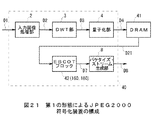
(2−1−1)符号化装置40の全体構成
図46との対応部分に同一符号を付して示す図21は、JPEG2000規格に準拠した本実施の形態による符号化装置40を示し、全体として一体にIC化(集積回路化)されて構成されている点と、ICの外部に量子化部4から出力されるコードブロックデータD4を記憶保持するDRAM41が設けられている点と、EBCOTブロック42の構成が異なる点とを除いて図46に示す符号化装置1と同様に構成されている。
(2) First Embodiment (2-1) Configuration of Encoding Device 40 according to First Embodiment (2-1-1) Overall Configuration of Encoding Device 40 Same reference numerals are assigned to corresponding parts to FIG. 21 shows the encoding device 40 according to the present embodiment compliant with the JPEG2000 standard, and is configured as an integrated IC (integrated circuit) as a whole, and outside the IC. The configuration is the same as that of the encoding device 1 shown in FIG. 46 except that a DRAM 41 for storing and holding the code block data D4 output from the quantization unit 4 is provided and that the configuration of the EBCOT block 42 is different. ing.

実際上、EBCOTブロック42においては、図22に示すように、それぞれSRAMからなる正負符号プレーンバッファ50及び処理ビットプレーンバッファ51A、51Bが入力段に設けられており、DRAM41(図21)に記憶保持されたコードブロックデータD4のうち、正負符号ビットプレーン22Sのデータ(以下、これを単に正負符号プレーンデータと呼ぶ)D20と、必要な処理ビットプレーン22のデータ(以下、これを単に処理ビットプレーンデータと呼ぶ)D21とを読み出し、これらをそれぞれSRAMでなる正負符号バッファ50又はビットプレーンバッファ51A、51Bに記憶保持し得るようになされている。   In practice, in the EBCOT block 42, as shown in FIG. 22, the positive / negative sign plane buffer 50 and the processing bit plane buffers 51A and 51B, each of which is an SRAM, are provided in the input stage and stored in the DRAM 41 (FIG. 21). Among the coded code block data D4, data of the positive / negative sign bit plane 22S (hereinafter, simply referred to as positive / negative sign plane data) D20 and necessary data of the processing bit plane 22 (hereinafter referred to simply as processing bit plane data). D21) is read out, and these can be stored and held in the positive / negative sign buffer 50 or the bit-plane buffers 51A and 51B made of SRAM, respectively.

この場合処理ビットプレーンバッファ51A、51Bは2つ設けられており、これにより一方の処理ビットプレーンバッファ51A、51Bに記憶保持した処理ビットプレーンデータD21をCBM処理しながら、他方の処理ビットプレーンバッファ51B、51Aに次の処理ビットプレーンデータD21を書き込み得るようになされている。   In this case, two processing bit plane buffers 51A and 51B are provided, whereby the processing bit plane data D21 stored and held in one processing bit plane buffer 51A and 51B is processed by the CBM, while the other processing bit plane buffer 51B. , 51A can be written with the next processing bit plane data D21.

またEBCOTブロック42には、それぞれ少なくとも1ビットプレーン分のデータ及び2ビットプレーン分のデータの記憶容量を有するSRAM52A、52Bが設けられており、これによりCBM処理時に利用するSIGプレーン31(図10)のデータ(以下、これをSIGプレーンデータと呼ぶ)D22をSRAM52Aに記憶保持し、REFプレーン32(図10)のデータ(以下、これをREFプレーンデータと呼ぶ)D23及びDONEプレーン33(図10)のデータ(以下、これをDONEプレーンデータと呼ぶ)D24をSRAM52Bに記憶保持することができるようになされている。   In addition, the EBCOT block 42 is provided with SRAMs 52A and 52B each having a storage capacity of at least data for 1 bit plane and data for 2 bit planes, whereby the SIG plane 31 (FIG. 10) used during CBM processing. Data (hereinafter referred to as SIG plane data) D22 is stored and held in the SRAM 52A, and data (hereinafter referred to as REF plane data) D23 and DONE plane 33 (FIG. 10) of the REF plane 32 (FIG. 10). The data (hereinafter referred to as DONE plane data) D24 can be stored and held in the SRAM 52B.

一方、処理ビットプレーンバッファ51A、51Bに記憶保持された処理ビットプレーンデータD21は、スイッチャ53を介してビットモデル部54により所定単位で順次読み出される。そしてビットモデル部54は、この読み出した処理ビットプレーンデータD21を、正負符号プレーンバッファ50に記憶保持された正負符号プレーンデータD20と、SRAM52A、52Bに記憶保持されたSIGプレーンデータD22、REFプレーンデータD23及びDONEプレーンデータD24とを利用しながらCBM処理し、かくして得られたシンボルSB及びコンテクストCXを算術符号化部55に送出する。   On the other hand, the processing bit plane data D21 stored and held in the processing bit plane buffers 51A and 51B is sequentially read out in predetermined units by the bit model unit 54 via the switcher 53. The bit model unit 54 then processes the read processed bit plane data D21 with the positive / negative code plane data D20 stored and held in the positive / negative code plane buffer 50, and the SIG plane data D22 and REF plane data stored and held in the SRAMs 52A and 52B. CBM processing is performed using D23 and DONE plane data D24, and the symbol SB and context CX thus obtained are sent to the arithmetic coding unit 55.

算術符号化部55は、供給されるシンボルSB及びコンテクストCXを入力として算術符号化処理を行いながら符号化列を生成し、かくして得られた符号化データD25をコードブロック20ごとに第1又は第2のビットストリームバッファ56A、56Bに順次交互に格納する。   The arithmetic encoding unit 55 generates an encoded sequence while performing arithmetic encoding processing with the supplied symbol SB and context CX as input, and the encoded data D25 thus obtained is first or second for each code block 20. The two bit stream buffers 56A and 56B are alternately stored.

そしてこの第1又は第2のビットストリームバッファ56A、56Bに格納された符号化データD25は、この後スイッチャ57を介して後段のパケッタイズ・ストリーム生成部8(図21)に送出される。   The encoded data D25 stored in the first or second bit stream buffer 56A, 56B is then sent to the subsequent packetized stream generation unit 8 (FIG. 21) via the switcher 57.

このようにしてこの符号化装置40においては、DRAM41に格納されたコードブロックデータD4から必要な処理ビットプレーンデータD21のみを読み出してビットプレーンバッファ51A、51Bに記憶保持しながら、当該記憶保持した処理ビットプレーンデータD21に対して順次CBM処理を施し得るようになされている。   In this way, in the encoding device 40, only the necessary processing bit plane data D21 is read from the code block data D4 stored in the DRAM 41 and stored in the bit plane buffers 51A and 51B, while the stored processing is performed. The bit plane data D21 can be sequentially subjected to CBM processing.

(2−1−2)ビットモデル部54の構成
ここでビットモデル部54は、図23に示すように、シグナルスイッチャ60、SPパス符号化処理部61、MRパス符号化処理部62、CUパス符号化処理部63、出力スイッチャ64及び制御部65から構成されている。
(2-1-2) Configuration of Bit Model Unit 54 Here, as shown in FIG. 23, the bit model unit 54 includes a signal switcher 60, an SP path encoding processing unit 61, an MR path encoding processing unit 62, and a CU path. It comprises an encoding processing unit 63, an output switcher 64, and a control unit 65.

この場合シグナルスイッチャ60は、トップビットプレーン22T以外の処理ビットプレーン22に対するCBM処理時、シーケンサ及びタイミングジェネレータとしての機能を有する制御部65の制御のもとに、処理ビットプレーンデータD21を、図24(A)に示す1ストライプカラム23Aを構成する4画素分を1ワードとして、ビットプレーン内スキャン順序に従って処理ビットプレーンバッファ51A、51Bから1ワードずつ順次読み出し、これをまずSPパス符号化処理部61に送出する。   In this case, the signal switcher 60 converts the processing bit plane data D21 into the processing bit plane data D21 under the control of the control unit 65 having functions as a sequencer and a timing generator during CBM processing for the processing bit planes 22 other than the top bit plane 22T. The four pixels constituting one stripe column 23A shown in (A) are taken as one word, and sequentially read out from the processing bit plane buffers 51A and 51B one by one in accordance with the scan order within the bit plane. To send.

またシグナルスイッチャ60は、これと同期して、処理ビットプレーンバッファ51A、51Bから読み出された4画素分の処理ビットプレーンデータD21に対してSPパスによる符号化処理(以下、これをSPパス符号化処理と呼ぶ)をする際に必要となる、当該4画素とそれぞれ同座標にある正負符号プレーン30上の4ビット及びその上下の各ビット(合わせて6ビット、図24(C)参照)の正負符号プレーンデータD20を正負符号プレーンバッファ50から順次読み出し、これをSPパス符号化処理部61に送出する。   Further, in synchronization with this, the signal switcher 60 encodes the processing bit plane data D21 for four pixels read out from the processing bit plane buffers 51A and 51B by the SP pass (hereinafter referred to as the SP pass code). 4 bits on the positive / negative sign plane 30 and the respective upper and lower bits (6 bits in total, refer to FIG. 24C), which are necessary when performing the conversion processing) The plus / minus sign plane data D20 is sequentially read from the plus / minus sign plane buffer 50 and sent to the SP pass encoding processing unit 61.

この場合正負符号プレーンバッファ50は、処理ビットプレーン22の各ストライプカラム23Aとそれぞれ対応する4画素分を単位(ワード)として正負符号プレーンデータD20を記憶しており、このワード単位で正負符号プレーンデータD20を読書きし得るように構成されている。従って、このときシグナルスイッチャ60は、かかる処理ビットプレーンバッファ51A、51Bから読み出された4画素分の処理ビットプレーンデータD21をSPパス符号化処理する際に必要となる合計6ビットの正負符号プレーンデータD20に対して、図25に示すように、実際には当該4画素とそれぞれ同座標にある正負符号プレーン30上の4画素分の正負符号プレーンデータD20と、その上下のストライプカラム23Aをそれぞれ構成する各4画素分の正負符号プレーンデータD20とを正負符号プレーンバッファ30から3クロックかけて順次読み出し、これをSPパス符号化処理部61に送出することとなる。   In this case, the plus / minus sign plane buffer 50 stores the plus / minus sign plane data D20 in units of four pixels corresponding to the respective stripe columns 23A of the processing bit plane 22 (words). D20 can be read and written. Therefore, at this time, the signal switcher 60 adds a total of 6 bits of positive / negative code planes necessary for SP pass encoding processing of the processing bit plane data D21 for four pixels read from the processing bit plane buffers 51A and 51B. For the data D20, as shown in FIG. 25, the positive / negative code plane data D20 for the four pixels on the positive / negative code plane 30 at the same coordinates as the four pixels and the upper and lower stripe columns 23A are actually The positive / negative code plane data D20 for each of the four pixels constituting the data is sequentially read from the positive / negative code plane buffer 30 over 3 clocks, and this is sent to the SP pass encoding processing unit 61.

さらにシグナルスイッチャ60は、これと同期して、かかる4画素分の処理ビットプレーンデータD21をSPパス符号化処理する際に必要となる、当該4画素とそれぞれ同座標にあるSIGプレーン31上の4ビット及びその上下の各ビット(合計6ビット、図24(B)参照)分のSIGプレーンデータD22をSRAM52Aから順次読み出し、これをSPパス符号化処理部61に送出する。   Furthermore, in synchronization with this, the signal switcher 60 is required to perform the SP pass encoding processing on the processing bit plane data D21 for the four pixels, and the four on the SIG plane 31 at the same coordinates as the four pixels. The SIG plane data D22 for the bits and the upper and lower bits (6 bits in total, see FIG. 24B) are sequentially read out from the SRAM 52A and sent to the SP pass encoding processing unit 61.

この場合SRAM52Aも、処理ビットプレーン22の各ストライプカラム23Aとそれぞれ対応する4画素分を単位(ワード)としてSIGプレーンデータD22を記憶しており、このワード単位でSIGプレーンデータD22を読書きし得るように構成されている。従って、このときシグナルスイッチャ60は、かかる処理ビットプレーンバッファ51A、51Bから読み出された4画素分の処理ビットプレーンデータD21をSPパス符号化処理する際に必要となる合計6ビット分のSIGプレーンデータD22に対して、実際には当該4画素とそれぞれ同座標にあるSIGプレーン31上の4ビットのSIGプレーンデータD22と、その上下の各4ビット分のSGIプレーンデータD22とをSRAM52Aから3クロックかけて順次読み出し(図25)、これをSPパス符号化処理部61に送出することとなる。   In this case, the SRAM 52A also stores the SIG plane data D22 in units (words) of four pixels respectively corresponding to the stripe columns 23A of the processing bit plane 22, and can read and write the SIG plane data D22 in units of words. It is configured as follows. Therefore, at this time, the signal switcher 60 performs a SIG plane for a total of 6 bits necessary for SP-pass encoding processing bit plane data D21 for 4 pixels read from the processing bit plane buffers 51A and 51B. For the data D22, the 4-bit SIG plane data D22 on the SIG plane 31 and the SGI plane data D22 for the upper and lower 4 bits on the SIG plane 31 at the same coordinates as the four pixels are actually transferred from the SRAM 52A by 3 clocks. The data are sequentially read (FIG. 25) and sent to the SP pass encoding processing unit 61.

さらにシグナルスイッチャ60は、これと同期して、かかる4画素分の処理ビットプレーンデータD21をSPパス符号化処理する際に必要となる、当該4画素とそれぞれ同座標にあるREFプレーン32上の4ビット(図24(E)参照)分のREFプレーンデータD23と、当該4画素と同座標にあるDONEプレーン33上の4ビット(図24(D)参照)分のDONEプレーンデータD24とをSRAM52Bから順次読み出し、これをSPパス符号化処理部61に送出する。   Further, the signal switcher 60 synchronizes with this, and the 4 bits on the REF plane 32 respectively having the same coordinates as the four pixels, which are necessary when the processing bit plane data D21 for the four pixels are subjected to the SP pass encoding process. From the SRAM 52B, the REF plane data D23 for bits (see FIG. 24E) and the DONE plane data D24 for 4 bits (see FIG. 24D) on the DONE plane 33 at the same coordinates as the four pixels are obtained from the SRAM 52B. The data are sequentially read out and sent to the SP pass encoding processing unit 61.

この場合SRAM52Bも、処理ビットプレーン22の各ストライプカラム23Aとそれぞれ対応する4画素分を単位(ワード)としてREFプレーンデータD23及びDONEプレーンデータD23を記憶しており、このワード単位でREFプレーンデータD23やDONEプレーンデータD23を読書きし得るように構成されている。従って、シグナルスイッチャ60は、かかる4ビット分のREFプレーンデータD23又はDONEプレーンデータD24をそれぞれ1クロックでSRAM52Bから読み出し、これをSPパス符号化処理部61に送出することとなる。   In this case, the SRAM 52B also stores the REF plane data D23 and the DONE plane data D23 in units (words) of four pixels respectively corresponding to the stripe columns 23A of the processing bit plane 22, and the REF plane data D23 in units of words. And DONE plane data D23 can be read and written. Therefore, the signal switcher 60 reads the 4-bit REF plane data D23 or DONE plane data D24 from the SRAM 52B in one clock, and sends it to the SP path encoding processing unit 61.

このときSPパス符号化処理部61は、シグナルスイッチャ60から順次供給される処理ビットプレーンデータD21と、これと対応する正負符号プレーンデータD20、SIGプレーンデータD22、REFプレーンデータD23及びDONEプレーンデータD24とを、それぞれ少なくとも過去3サンプル分だけ記憶保持し得るようになされている。   At this time, the SP path encoding processing unit 61 sequentially processes bit plane data D21 supplied from the signal switcher 60, and corresponding positive / negative code plane data D20, SIG plane data D22, REF plane data D23, and DONE plane data D24. Can be stored and held for at least the past three samples.

因みに、ここでは処理ビットプレーンデータD21、REFプレーンデータD23及びDONEプレーンデータD24については1ワードが1サンプルに該当し、正負符号プレーンデータD20及びSIGプレーンデータD22については縦方向に並ぶ3ワードが1サンプルに該当する。   Incidentally, here, one word corresponds to one sample for the processing bit plane data D21, the REF plane data D23, and the DONE plane data D24, and three words arranged in the vertical direction for the positive / negative code plane data D20 and the SIG plane data D22 are one. Applicable to the sample.

そしてSPパス符号化処理部61は、シグナルスイッチャ60から次のサンプルの処理ビットプレーンデータD21等が与えられると、その1つ前のサンプルの処理ビットプレーンデータD21(図24(A)において太枠で囲んだ4画素分)について、そのとき記憶保持している図24(B)〜(E)においてそれぞれ太枠で囲まれたSIGプレーンデータD22、正負符号プレーンデータD20、REFプレーンデータD23及びDONEプレーンデータD24を利用して、SPパス符号化処理できるか否かの検出と、できる場合のSPパス符号化処理とを実行する。   Then, when the processing sample bit plane data D21 of the next sample is given from the signal switcher 60, the SP pass encoding processing unit 61 receives the processing bit plane data D21 of the previous sample (in FIG. 24A, the thick frame). 24 (B) to (E) stored and held at that time, the SIG plane data D22, the positive / negative code plane data D20, the REF plane data D23, and the DONE, respectively, surrounded by a thick frame in FIG. The plain data D24 is used to detect whether or not the SP pass encoding process can be performed, and to perform the SP pass encoding process when possible.

そしてSPパス符号化処理部61は、SPパス符号化処理を行った場合、これにより得られたその画素についてのシンボルSB及び正負符号についての各シンボルSBをシンボルデータD26Sとして出力スイッチャ64に送出すると共に、その画素についてのコンテクストCX及び正負符号についてのコンテクストCXをコンテクストデータD27Sとして出力スイッチャ64に送出する。   When performing the SP pass encoding process, the SP pass encoding processing unit 61 sends the symbol SB for the pixel and the symbol SB for the positive / negative code obtained thereby to the output switcher 64 as symbol data D26S. At the same time, the context CX for the pixel and the context CX for the sign are sent to the output switcher 64 as context data D27S.

またSPパス符号化処理部61は、SPパス符号化処理を行ったときは、かかるSIGプレーンデータD22、REFプレーンデータD23及び又はDONEプレーンデータD24をこれに応じて更新し、その後これらをシグナルスイッチ60を介して対応するSRAM52A、52Bに与えることにより、これらSIGプレーンデータD22、REFプレーンデータD23及びDONEプレーンデータD24をそれぞれSRAM52A、52Bにおけるもとのアドレス位置に書き戻させる(Read-Modify-Write)。   Further, when the SP path encoding processing unit 61 performs the SP path encoding process, the SP path encoding process 61 updates the SIG plane data D22, the REF plane data D23, and / or the DONE plane data D24 accordingly, and then updates them to the signal switch. By giving the data to the corresponding SRAMs 52A and 52B via 60, the SIG plane data D22, REF plane data D23 and DONE plane data D24 are written back to the original address positions in the SRAMs 52A and 52B, respectively (Read-Modify-Write ).

一方、シグナルスイッチャ60は、このようにして処理ビットプレーンバッファ51A、51Bに格納された1ビットプレーン分のデータ(処理ビットプレーンデータD21)に対するSPパス符号化処理を終了すると、この後これと同様にして、制御部65の制御のもとに、同じ処理ビットプレーンデータD21を、図24(A)に示す1ストライプカラム23Aを構成する4画素分を1ワードとして、ビットプレーン内スキャン順序に従って処理ビットプレーンバッファ51A、51Bから1ワードずつ順次読み出し、これをMRパス符号化処理部62に送出する。   On the other hand, when the signal switcher 60 finishes the SP pass encoding process for the data for one bit plane (processed bit plane data D21) stored in the processed bit plane buffers 51A and 51B in this way, the same processing is performed thereafter. Then, under the control of the control unit 65, the same processing bit plane data D21 is processed in accordance with the scan order within the bit plane, with 4 pixels constituting one stripe column 23A shown in FIG. The word plane buffers 51A and 51B are sequentially read one word at a time and sent to the MR pass encoding processing unit 62.

またシグナルスイッチャ60は、これと同期して、処理ビットプレーンバッファ51A、51Bから読み出された4画素分の処理ビットプレーンデータD21に対してMRパスによる符号化処理(以下、これをMRパス符号化処理と呼ぶ)をする際に必要となる、当該4画素とそれぞれ同座標にあるSIGプレーン31上の4ビット及びその上下の各ビット(合わせて6ビット、図24(B)参照)のSIGプレーンデータD22をSRAM52Aから順次読み出し、これをMRパス符号化処理部62に送出する。   Further, in synchronization with this, the signal switcher 60 encodes the processing bit plane data D21 for four pixels read from the processing bit plane buffers 51A and 51B by MR pass (hereinafter referred to as MR pass code). SIG of 4 bits on the SIG plane 31 and the upper and lower bits (6 bits in total, refer to FIG. 24B) required for the four pixels at the same coordinates. The plane data D22 is sequentially read from the SRAM 52A and sent to the MR pass encoding processing unit 62.

この際シグナルスイッチャ60は、上述のSPパス符号化処理部61の場合と同様に、かかる処理ビットプレーンバッファ51A、51Bから読み出された4画素分の処理ビットプレーンデータD21をMRパス符号化処理する際に必要となる合計6ビット分のSIGプレーンデータに対して、実際には当該4画素とそれぞれ同座標にあるSIGプレーン31上の4ビット分のSIGプレーンデータD22と、その上下の各4ビット分のSIGプレーンデータD22とをSRAM52Aから3クロックかけて順次読み出し(図25)、これをMRパス符号化処理部62に送出することとなる。   At this time, as in the case of the SP pass encoding processing unit 61 described above, the signal switcher 60 performs MR pass encoding processing on the processed bit plane data D21 for four pixels read from the processing bit plane buffers 51A and 51B. For the SIG plane data for a total of 6 bits required for the SIG plane data, actually, the SIG plane data D22 for 4 bits on the SIG plane 31 at the same coordinates as the four pixels, and the upper and lower 4 The SIG plane data D22 for bits is sequentially read from the SRAM 52A over 3 clocks (FIG. 25), and is sent to the MR pass encoding processing unit 62.

さらにシグナルスイッチャ60は、これと同期して、かかる4画素分の処理ビットプレーンデータD21をMRパス符号化処理する際に必要となる、当該4画素と同座標にあるREFプレーン32上の1ワード(図24(E)参照)分のREFプレーンデータD23と、当該4画素と同座標にあるDONEプレーン33上の1ワード(図24(D)参照)分のDONEプレーンデータD24とをSRAM52Bから順次読み出し、これをMRパス符号化処理部61に送出する。   Further, the signal switcher 60 synchronizes with this, and one word on the REF plane 32 at the same coordinates as the four pixels, which is necessary when the processing bit plane data D21 for the four pixels is subjected to MR pass encoding processing. REF plane data D23 (see FIG. 24 (E)) and DONE plane data D24 for one word (see FIG. 24 (D)) on the DONE plane 33 at the same coordinates as the four pixels are sequentially stored from the SRAM 52B. This is read out and sent to the MR pass encoding processing unit 61.

このときMRパス符号化処理部62は、シグナルスイッチャ60から順次供給される4画素分の処理ビットプレーンデータD21と、これと対応するSIGプレーンデータD22、REFプレーンデータD23及びDONEプレーンデータD24とを、それぞれ少なくとも過去3サンプル分だけ記憶保持し得るようになされている。   At this time, the MR pass encoding processing unit 62 receives the processing bit plane data D21 for four pixels sequentially supplied from the signal switcher 60, and the corresponding SIG plane data D22, REF plane data D23, and DONE plane data D24. In each case, at least the past three samples can be stored and held.

因みに、この場合も処理ビットプレーンデータD21、REFプレーンデータD23及びDONEプレーンデータD24については1ワードが1サンプルに該当し、正負符号プレーンデータD20及びSIGプレーンデータD22については縦方向に並ぶ3ワードが1サンプルに該当する。   Incidentally, also in this case, one word corresponds to one sample for the processing bit plane data D21, the REF plane data D23, and the DONE plane data D24, and three words arranged in the vertical direction for the positive / negative code plane data D20 and the SIG plane data D22. It corresponds to one sample.

そしてMRパス符号化処理部62は、シグナルスイッチャ60から次のサンプルの処理ビットプレーンデータD21等が与えられると、その1つ前のサンプルの処理ビットプレーンデータD21(図24(A)において太枠で囲んだ4画素分)について、そのとき記憶保持している図24(B)、(D)及び(E)においてそれぞれ太枠で囲まれた必要なSIGプレーンデータD22、REFプレーンデータD23及びDONEプレーンデータD24を利用して、MRパス符号化処理できるか否かの検出と、できる場合のMRパス符号化処理とを実行する。   Then, when the processing bit plane data D21 of the next sample is given from the signal switcher 60, the MR pass encoding processing unit 62 receives the processing bit plane data D21 of the previous sample (in FIG. 24A), the thick frame 4 pixels), the necessary SIG plane data D22, REF plane data D23, and DONE enclosed in thick frames in FIGS. 24B, 24D, and 24E respectively stored at that time. The plain data D24 is used to detect whether or not the MR pass encoding process can be performed, and to perform the MR pass encoding process when possible.

そしてMRパス符号化処理部62は、MRパス符号化処理を行った場合、これにより得られたその画素についてのシンボルSB及び正負符号についてのシンボルSBをシンボルデータD26Rとして出力スイッチャ64に送出すると共に、その画素についてのコンテクストCX及び正負符号についてのコンテクストCXをコンテクストデータD27Rとして出力スイッチャ64に送出する。   When the MR pass encoding processing is performed, the MR pass encoding processing unit 62 sends the symbol SB for the pixel and the symbol SB for the positive / negative code obtained thereby to the output switcher 64 as symbol data D26R. The context CX for the pixel and the context CX for the positive / negative sign are sent to the output switcher 64 as context data D27R.

またMRパス符号化処理部62は、MRパス符号化処理を行ったときは、SIGプレーンデータD22、REFプレーンデータD23及び又はDONEプレーンデータD24をこれに応じて更新し、その後これらをシグナルスイッチ60を介して対応するSRAM52A、52Bに与えることにより、これらSIGプレーンデータD22、REFプレーンデータD23及びDONEプレーンデータD24をそれぞれSRAM52A、52Bにおけるもとのアドレス位置に書き戻させる(Read-Modify-Write)。   Further, when the MR path encoding process is performed, the MR path encoding processing unit 62 updates the SIG plane data D22, the REF plane data D23 and / or the DONE plane data D24 accordingly, and thereafter updates them to the signal switch 60. To the corresponding SRAMs 52A and 52B, the SIG plane data D22, REF plane data D23, and DONE plane data D24 are written back to the original address positions in the SRAMs 52A and 52B, respectively (Read-Modify-Write). .

他方、シグナルスイッチャ60は、このようにして処理ビットプレーンバッファ51A、51Bに格納された1ビットプレーン分のデータ(処理ビットプレーンデータD21)に対するMRパス符号化処理を終了すると、この後これと同様にして、制御部65の制御のもとに、同じ処理ビットプレーンデータD21を、図24(A)に示す1ストライプカラム23Aを構成する4画素分を1ワードとして、ビットプレーン内スキャン順序に従って処理ビットプレーンバッファ51A、51Bから1ワードずつ順次読み出し、これをCUパス符号化処理部63に送出する。   On the other hand, when the signal switcher 60 finishes the MR pass encoding process for the data for one bit plane (processed bit plane data D21) stored in the processed bit plane buffers 51A and 51B in this way, the same processing is performed thereafter. Then, under the control of the control unit 65, the same processing bit plane data D21 is processed in accordance with the scan order within the bit plane, with 4 pixels constituting one stripe column 23A shown in FIG. The word plane buffers 51A and 51B are sequentially read one word at a time and sent to the CU pass encoding processing unit 63.

またシグナルスイッチャ60は、これと同期して、処理ビットプレーンバッファ51A、51Bから読み出された4画素分の処理ビットプレーンデータD21に対してCUパスによる符号化処理(以下、これをCUパス符号化処理と呼ぶ)をする際に必要となる、当該4画素とそれぞれ同座標にある正負符号プレーン30上の4ビット及びその上下の各ビット(合わせて6ビット、図24(C)参照)分の正負符号プレーンデータD20を正負符号プレーンバッファ50から順次読み出し、これをCUパス符号化処理部63に送出する。   In synchronization with this, the signal switcher 60 encodes the processing bit plane data D21 for four pixels read from the processing bit plane buffers 51A and 51B by the CU pass (hereinafter referred to as CU pass code). 4 bits on the positive / negative sign plane 30 and the upper and lower bits (6 bits in total, refer to FIG. 24C) necessary for the four pixels and having the same coordinates. The positive / negative code plane data D20 are sequentially read from the positive / negative code plane buffer 50 and sent to the CU pass encoding processing unit 63.

この際シグナルスイッチャ60は、上述のSPパス符号化処理部61と同様に、かかる処理ビットプレーンバッファ51A、51Bから読み出された4画素分の処理ビットプレーンデータD21をCUパス符号化処理する際に必要となる合計6ビットの正負符号プレーンデータD21に対して、実際には当該4画素とそれぞれ同座標にある正負符号プレーン30上の1ストライプカラム23Aを構成する4ビット分の正負符号プレーンデータD20と、その上下のストライプカラム23Aをそれぞれ構成する各4ビットの正負符号プレーンデータD20とを正負符号プレーンバッファ50から3クロックかけて順次読み出し、これをCUパス符号化処理部62に送出することとなる。   At this time, the signal switcher 60 performs the CU pass encoding process on the processing bit plane data D21 for four pixels read out from the processing bit plane buffers 51A and 51B in the same manner as the SP pass encoding processing unit 61 described above. 4 bits plus / minus sign plane data that constitutes one stripe column 23A on the plus / minus sign plane 30 that is actually at the same coordinates as the four pixels, in contrast to the 6 bits plus / minus sign plane data D21 required for D20 and the 4-bit positive / negative code plane data D20 respectively constituting the upper and lower stripe columns 23A are sequentially read from the positive / negative code plane buffer 50 over 3 clocks and sent to the CU pass encoding processing unit 62. It becomes.

さらにシグナルスイッチャ60は、これと同期して、かかる4画素分の処理ビットプレーンデータD21をCUパス符号化処理する際に必要となる、当該4画素とそれぞれ同座標にあるSIGプレーン31上の4ビット及びその上下の各ビット(合計6ビット、図24(B)参照)分のSIGプレーンデータD22をSRAM52Aから順次読み出し、これをCUパス符号化処理部63に送出する。   Further, in synchronization with this, the signal switcher 60 is required to perform the CU pass encoding process on the processing bit plane data D21 for the four pixels, and the four on the SIG plane 31 at the same coordinates as the four pixels. The SIG plane data D22 for the bits and the upper and lower bits (6 bits in total, see FIG. 24B) are sequentially read from the SRAM 52A, and sent to the CU pass encoding processing unit 63.

この場合においても、シグナルスイッチャ60は、かかる処理ビットプレーンバッファ51A、51Bから読み出された4画素分の処理ビットプレーンデータD21をCUパス符号化処理する際に必要となる合計6ビット分のSIGプレーンデータに対して、実際には当該4画素とそれぞれ同座標にあるSIGプレーン31上の4ビットのSIGプレーンデータD22と、その上下の各4ビット分のSIGプレーンデータD22とをSRAM52Aから3クロックかけて順次読み出し(図25)、これをCUパス符号化処理部63に送出することとなる。   In this case as well, the signal switcher 60 is a SIG for a total of 6 bits that is required when the processing bit plane data D21 for 4 pixels read from the processing bit plane buffers 51A and 51B is subjected to CU pass encoding processing. For the plane data, in reality, 4 bits of SIG plane data D22 on the SIG plane 31 at the same coordinates as the 4 pixels and 4 bits of SIG plane data D22 for each of the upper and lower sides thereof are transferred from the SRAM 52A by 3 clocks. The data are sequentially read (FIG. 25) and sent to the CU pass encoding processing unit 63.

さらにシグナルスイッチャ60は、これと同期して、かかる4画素分の処理ビットプレーンデータD21をCUパス符号化処理する際に必要となる、当該4画素とそれぞれ同座標にあるREFプレーン32上の1ワード(図24(E)参照)分のREFプレーンデータD23と、当該4画素と同座標にあるDONEプレーン33上の1ワード(図24(D)参照)分のDONEプレーンデータD24とをSRAM52Bから読み出し、これをCUパス符号化処理部63に送出する。   Further, in synchronization with this, the signal switcher 60 is required to process the 4-bit processing bit-plane data D21 for CU pass encoding, and the 1 on the REF plane 32 at the same coordinates as the 4 pixels. From the SRAM 52B, the REF plane data D23 for the word (see FIG. 24E) and the DONE plane data D24 for one word (see FIG. 24D) on the DONE plane 33 at the same coordinates as the four pixels are obtained from the SRAM 52B. This is read out and sent to the CU pass encoding processing unit 63.

このときCUパス符号化処理部63は、シグナルスイッチャ60から順次供給される4画素分の処理ビットプレーンデータD21と、これと対応する正負符号プレーンデータD20、SIGプレーンデータD22、REFプレーンデータD23及びDONEプレーンデータD24とを、それぞれ少なくとも過去3サンプル分だけ記憶保持し得るようになされている。   At this time, the CU pass encoding processing unit 63 processes the 4-bit processing bit plane data D21 sequentially supplied from the signal switcher 60, the corresponding positive / negative code plane data D20, SIG plane data D22, REF plane data D23, and The DONE plane data D24 can be stored and held for at least the past three samples.

因みに、この場合も処理ビットプレーンデータD21、REFプレーンデータD23及びDONEプレーンデータD24については1ワードが1サンプルに該当し、正負符号プレーンデータD20及びSIGプレーンデータD22については縦方向に並ぶ3ワードが1サンプルに該当する。   Incidentally, also in this case, one word corresponds to one sample for the processing bit plane data D21, the REF plane data D23, and the DONE plane data D24, and three words arranged in the vertical direction for the positive / negative code plane data D20 and the SIG plane data D22. It corresponds to one sample.

そしてCUパス符号化処理部63は、シグナルスイッチャ60から次のサンプルの処理ビットプレーンデータD21等が与えられると、その1つ前のサンプルの処理ビットプレーンデータD21(図24(A)において太枠で囲んだ4画素分)について、そのとき記憶保持している図24(B)〜(E)においてそれぞれ太枠で囲まれたSIGプレーンデータD22、正負符号プレーンデータD20、REFプレーンデータD23及びDONEプレーンデータD24を利用して、CUパス符号化処理できるか否かの検出と、できる場合のCUパス符号化処理とを実行する。   Then, when the processing bit plane data D21 of the next sample is given from the signal switcher 60, the CU pass encoding processing unit 63 receives the processing bit plane data D21 of the previous sample (in FIG. 24A, a thick frame). 24 (B) to (E) stored and held at that time, the SIG plane data D22, the positive / negative code plane data D20, the REF plane data D23, and the DONE, respectively, surrounded by a thick frame in FIG. The plain data D24 is used to detect whether or not the CU path encoding process can be performed and to perform the CU path encoding process when possible.

そしてCUパス符号化処理部63は、CUパス符号化処理を行った場合、これにより得られたその画素についてのシンボルSB及び正負符号についてのシンボルSBをシンボルデータD26Cとして出力スイッチャ64に送出すると共に、その画素についてのコンテクストCX及び正負符号についてのコンテクストCXをコンテクストデータD27Cとして出力スイッチャ64に送出する。   When the CU pass encoding processing is performed, the CU pass encoding processing unit 63 sends the symbol SB for the pixel and the symbol SB for the positive / negative code obtained thereby to the output switcher 64 as symbol data D26C. The context CX for the pixel and the context CX for the positive / negative sign are sent to the output switcher 64 as context data D27C.

またCUパス符号化処理部63は、CUパス符号化処理を行ったときは、かかるSIGプレーンデータD22、REFプレーンデータD23及び又はDONEプレーンデータD24をこれに応じて更新し、その後これらをシグナルスイッチ60を介して対応するSRAM52A、52Bに与えることにより、これらSIGプレーンデータD22、REFプレーンデータD23及びDONEプレーンデータD24をそれぞれSRAM52A、52Bにおけるもとのアドレス位置に書き戻させる(Read-Modify-Write)。   In addition, when the CU path encoding processing unit 63 performs the CU path encoding process, the SIG plane data D22, the REF plane data D23 and / or the DONE plane data D24 are updated accordingly, and then these are switched to the signal switch. By giving the data to the corresponding SRAMs 52A and 52B via 60, the SIG plane data D22, REF plane data D23 and DONE plane data D24 are written back to the original address positions in the SRAMs 52A and 52B, respectively (Read-Modify-Write ).

出力スイッチャ64においては、制御部65の制御のもとに、SPパス符号化処理部61、MRパス符号化処理部62及びCUパス符号化処理部63のそれぞれから与えられるシンボルデータD26S、D26R、D26Cと、コンテクストデータD27S、D27R、D27CとをそれぞれシンボルデータD26及びコンテクストデータD27として算術符号化部55に送出する。   In the output switcher 64, under the control of the control unit 65, the symbol data D26S, D26R, which are respectively given from the SP path encoding processing unit 61, the MR path encoding processing unit 62, and the CU path encoding processing unit 63, D26C and context data D27S, D27R, and D27C are sent to arithmetic coding unit 55 as symbol data D26 and context data D27, respectively.

このようにしてこのビットモデル部54においては、処理ビットプレーン22上のストライプカラム23Aを構成する4画素を単位としてSPパス符号化処理、MRパス符号化処理及びCUパス符号化処理を行うと共に、このとき正負符号プレーンデータD20及びSIGプレーンデータD22についても当該ストライプカラム23Aと同位相の1ストライプカラム23Aを構成する4ビットをメモリワードとすることにより、メモリアクセス回数を格段的に低減させて、CBM処理を確実に高速に行い得るようになされている。   In this manner, the bit model unit 54 performs the SP pass encoding process, the MR pass encoding process, and the CU pass encoding process in units of four pixels constituting the stripe column 23A on the processing bit plane 22. At this time, for the positive / negative sign plane data D20 and the SIG plane data D22, the number of memory accesses is significantly reduced by using 4 bits constituting one stripe column 23A in the same phase as the stripe column 23A as a memory word, The CBM process can be surely performed at high speed.

(2−1−3)各コーディング・パス処理部の具体的構成
次に、SPパス符号化処理部61、MRパス符号化処理部62及びCUパス符号化処理部63の各構成についてそれぞれ順番に説明する。
(2-1-3) Specific Configuration of Each Coding / Pass Processing Unit Next, each configuration of the SP path encoding processing unit 61, the MR path encoding processing unit 62, and the CU path encoding processing unit 63 is sequentially described. explain.

(2−1−3−1)SPパス符号化処理部61の構成
SPパス符号化処理部61は、図26に示すように、いずれもハードウェア構成の処理ビットシフトレジスタ部70、正符号シフトレジスタ部71、SIGシフトレジスタ部72、REFシフトレジスタ部73、DONEシフトレジスタ部74及びセレクタ75と、後述のようなセレクタ75に対する出力切替え制御等を行う制御部76とから構成されている。
(2-1-3-1) Configuration of SP Path Encoding Processing Unit 61 As shown in FIG. 26, the SP path encoding processing unit 61 includes a processing bit shift register unit 70 having a hardware configuration and a positive code shift. The register unit 71, the SIG shift register unit 72, the REF shift register unit 73, the DONE shift register unit 74, and the selector 75, and a control unit 76 that performs output switching control for the selector 75 as described later.

また処理ビットシフトレジスタ部70には3段のシフトレジスタ70Aが設けられると共に、正符号シフトレジスタ部71、SIGシフトレジスタ部72、REFシフトレジスタ部73及びDONEシフトレジスタ部74には、それぞれ4段のシフトレジスタ71A〜74Aが設けられている。   The processing bit shift register unit 70 is provided with a three-stage shift register 70A, and each of the positive sign shift register unit 71, the SIG shift register unit 72, the REF shift register unit 73, and the DONE shift register unit 74 has four stages. Shift registers 71A to 74A are provided.

これによりSPパス符号化処理部61は、上述のようにシグナルスイッチャ60(図23)から順次与えられる各1サンプル分の処理ビットプレーンデータD21、正負符号プレーンデータD20、SIGプレーンデータD22、REFプレーンデータD23及びDONEプレーンデータD24を、それぞれ処理ビットシフトレジスタ部70、正符号シフトレジスタ部71、SIGシフトレジスタ部72、REFシフトレジスタ部73及びDONEシフトレジスタ部74の各シフトレジスタ70A〜74Aにおいて順次シフトさせながら3サンプル分又は4サンプル分ずつ記憶保持し得るようになされている。   As a result, the SP pass encoding processing unit 61, as described above, sequentially processes one-sample processed bit plane data D21, positive / negative code plane data D20, SIG plane data D22, and REF plane from the signal switcher 60 (FIG. 23). The data D23 and the DONE plane data D24 are sequentially transferred to the processing bit shift register unit 70, the plus sign shift register unit 71, the SIG shift register unit 72, the REF shift register unit 73, and the shift registers 70A to 74A of the DONE shift register unit 74, respectively. While shifting, it is possible to store and hold 3 samples or 4 samples.

そして処理ビットシフトレジスタ部70は、シグナルスイッチャ60から1サンプル分の処理ビットプレーンデータD21が与えられると、このとき自己のシフトレジスタ70Aの2段目にシフトされた1サンプル分の処理ビットプレーンデータD21をセレクタ75に出力する。   The processing bit shift register 70 receives the processing bit plane data D21 for one sample from the signal switcher 60. At this time, the processing bit plane data for one sample shifted to the second stage of its own shift register 70A. D21 is output to the selector 75.

またこのときSIGシフトレジスタ部72は、これと同期して、自己のシフトレジスタ72Aに記憶保持したSIGプレーンデータD22を用いて、このとき処理ビットシフトレジスタ部70のシフトレジスタ70Aの2段目にシフトされた4画素について、それぞれ上述のSPパス符号化処理を行うための条件を満たしているか否かの検出処理を画素ごとに並行して行い、検出結果をセレクタ75に出力する。   At this time, the SIG shift register unit 72 uses the SIG plane data D22 stored and held in its own shift register 72A in synchronization with this, and at this time the second stage of the shift register 70A of the processing bit shift register unit 70 For the shifted four pixels, detection processing is performed in parallel for each pixel to determine whether or not the conditions for performing the above-described SP pass encoding processing are satisfied, and the detection result is output to the selector 75.

さらにSIGシフトレジスタ部72は、これと同期して、当該処理ビットシフトレジスタ部70のシフトレジスタ70Aの2段目にシフトされた4画素について、図13について上述したルールに従って、当該4画素ごとのコンテクストCXをそれぞれ演算し、演算結果をセレクタ75に出力する。   Further, in synchronization with this, the SIG shift register unit 72 synchronizes the four pixels shifted to the second stage of the shift register 70A of the processing bit shift register unit 70 according to the rule described above with reference to FIG. Each context CX is calculated and the calculation result is output to the selector 75.

そして、このときSIGシフトレジスタ部72により検出された、処理ビットシフトレジスタ部70のシフトレジスタ70Aの2段目にシフトされた4画素についてのSPパス符号化処理を行うための条件を満たしているか否かの検出結果が全て否定的であった場合には、セレクタ75からは何も出力されず、処理ビットシフトレジスタ部70のシフトレジスタ70Aの2段目にシフトされた1サンプル(4画素)分の処理ビットプレーンデータD21に対する処理が終了する。   Whether the conditions for performing the SP pass encoding processing for the four pixels shifted to the second stage of the shift register 70A of the processing bit shift register unit 70 detected by the SIG shift register unit 72 at this time are satisfied. If all the negative detection results are negative, nothing is output from the selector 75, and one sample (four pixels) shifted to the second stage of the shift register 70A of the processing bit shift register unit 70 The processing for the corresponding processing bit plane data D21 ends.

これに対して、処理ビットシフトレジスタ部70のシフトレジスタ70Aの2段目にシフトされた1サンプルのうちのいずれかの画素(以下、これをSPパス符号化処理対象画素と呼ぶ)についての検出結果が肯定的であった場合には、処理ビットシフトレジスタ部70から出力された当該SPパス符号化処理対象画素のデータ値(0/1)と、これに同期してSIGシフトレジスタ部72から出力された当該SPパス符号化処理対象画素についてのコンテクストCXの演算結果とが、それぞれそのSPパス符号化処理対象画素のシンボルSB及びコンテクストCXとしてセレクタ75から出力される。   On the other hand, detection of any pixel (hereinafter referred to as an SP pass encoding target pixel) of one sample shifted to the second stage of the shift register 70A of the processing bit shift register unit 70. If the result is affirmative, the data value (0/1) of the SP pass encoding target pixel output from the processing bit shift register unit 70 and the SIG shift register unit 72 in synchronization therewith. The output calculation result of the context CX for the SP pass encoding target pixel is output from the selector 75 as the symbol SB and the context CX of the SP pass encoding target pixel, respectively.

また、このシンボルSBの値が『0』であった場合、この後セレクタ75からDONEシフトレジスタ部74に与えられる更新情報に基づいて、当該DONEシフトレジスタ部74のシフトレジスタ74Aに記憶保持されたDONEプレーンデータD24のうち、SPパス符号化処理対象画素と同座標のビットの値が、ビットモデル化が完了したことを表す『1』に更新されて、このSPパス符号化処理対象画素に対するSPパス符号化処理が完了する。   When the value of the symbol SB is “0”, the symbol SB is stored and held in the shift register 74A of the DONE shift register unit 74 based on the update information given to the DONE shift register unit 74 from the selector 75 thereafter. In the DONE plane data D24, the value of the bit having the same coordinate as the SP pass encoding target pixel is updated to “1” indicating that the bit modeling is completed, and the SP for the SP pass encoding target pixel is updated. The pass encoding process is completed.

これに対して、このシンボルSBの値が『1』であった場合には、その情報がSIGシフトレジスタ部72、REFシフトレジスタ部73及び正負符号シフトレジスタ部71にそれぞれ与えられる。   On the other hand, when the value of the symbol SB is “1”, the information is given to the SIG shift register unit 72, the REF shift register unit 73, and the positive / negative sign shift register unit 71, respectively.

このときSIGシフトレジスタ部72では、自己のシフトレジスタ72Aに記憶保持されたSIGプレーンデータD22におけるSPパス符号化処理対象画素と同座標のビットの値が“Significant”であることを表す『1』に更新される。またREFシフトレジスタ部73では、自己のシフトレジスタ73Aに記憶保持されたREFプレーンデータD23におけるSPパス符号化処理対象画素と同座標のビットの値が、“Significant”となったことを表す『1』に更新される。   At this time, the SIG shift register unit 72 represents “1” indicating that the bit value of the same coordinate as the SP pass encoding target pixel in the SIG plane data D22 stored and held in its own shift register 72A is “Significant”. Updated to The REF shift register unit 73 indicates that the value of the bit having the same coordinate as the SP pass encoding target pixel in the REF plane data D23 stored and held in its own shift register 73A is “Significant”. Is updated.

さらにこのとき正負符号シフトレジスタ部71は、このSPパス符号化処理対象画素の正負符号のシンボルSB及びコンテクストCXを図14について上述したルールに従って演算し、その演算結果をセレクタ75に送出する。かくしてこのシンボルSB及びコンテクストCXがセレクタ75を介して出力される。   Further, at this time, the positive / negative code shift register unit 71 calculates the symbols SB and context CX of the positive / negative codes of this SP pass encoding target pixel according to the rules described above with reference to FIG. 14 and sends the calculation results to the selector 75. Thus, the symbol SB and the context CX are output via the selector 75.

そして、この後セレクタ75からDONEシフトレジスタ部74に更新情報与えられ、当該更新情報に基づき、DONEシフトレジスタ部74のシフトレジスタ74Aに記憶保持されたDONEプレーンデータD24におけるSPパス符号化処理対象画素と同座標のビットの値が『1』に更新されて、当該SPパス符号化処理対象画素に対するSPパス符号化処理が完了する。   Thereafter, update information is given to the DONE shift register unit 74 from the selector 75, and based on the update information, the SP pass encoding target pixel in the DONE plane data D24 stored and held in the shift register 74A of the DONE shift register unit 74 And the value of the bit at the same coordinate is updated to “1”, and the SP pass encoding process for the SP pass encoding target pixel is completed.

またSPパス符号化処理部61は、この後同じサンプル(このとき処理ビットシフトレジスタ部70のシフトレジスタ70Aの2段目に記憶保持された1サンプル)内の当該SPパス符号化処理対象画素よりもビットプレーン内スキャン順序が後の各画素について、SPパス符号化処理を行うための条件を満たしていない場合にはスキップし、SPパス符号化処理を行うための条件を満たしている場合には上述のSPパス符号化処理対象画素と同様にしてSPパス符号化処理を行う。そしてSPパス符号化処理部61は、このような処理を当該サンプル内の全ての画素に対して行い終えると、当該サンプルに対する処理を終了する。   Further, the SP pass encoding processing unit 61 thereafter uses the SP pass encoding processing target pixel in the same sample (one sample stored and held in the second stage of the shift register 70A of the processing bit shift register unit 70 at this time). If the conditions for performing the SP pass encoding process are not satisfied for each pixel whose scan order in the bit plane is later, the processing is skipped. If the conditions for performing the SP pass encoding process are satisfied, The SP pass encoding process is performed in the same manner as the above-described SP pass encoding target pixel. Then, the SP pass encoding processing unit 61 ends the processing for the sample after completing such processing for all the pixels in the sample.

そして、SPパス符号化処理部61は、この後制御部76から制御部65(図23)に与えられる次の1サンプル分の処理ビットプレーンデータD21等の転送要求に応じて、シグナルスイッチャ60から当該次の1サンプル分の処理ビットプレーンデータD21等が与えられるごとに同様の処理を順次繰り返す。   Then, in response to a transfer request for the processed bit-plane data D21 for the next one sample given from the control unit 76 to the control unit 65 (FIG. 23), the SP path encoding processing unit 61 receives the signal switcher 60 from the signal switcher 60. The same processing is sequentially repeated each time the processing bit plane data D21 for the next one sample is given.

またこの際SPパス符号化処理部61は、次の1サンプル分の処理ビットプレーンデータD21等が与えられるごとに、SIGシフトレジスタ部72、REFシフトレジスタ部73及びDONEシフトレジスタ部74の各シフトレジスタ72A〜74Aの4段目にそれぞれ記憶保持されたSIGプレーンデータD22、REFプレーンデータD23及びDONEプレーンデータD24をそれぞれシグナルスイッチ60を介して対応するSRAM52A、52Bに与えることにより、これらをSRAM52A、52Bのもとの位置に書き戻させる。   At this time, the SP pass encoding processing unit 61 applies each shift of the SIG shift register unit 72, the REF shift register unit 73, and the DONE shift register unit 74 each time the processing bit plane data D21 for the next one sample is given. The SIG plane data D22, REF plane data D23, and DONE plane data D24 stored and held in the fourth stage of each of the registers 72A to 74A are supplied to the corresponding SRAMs 52A and 52B via the signal switch 60, respectively. Write back to the original position of 52B.

このようにしてSPパス符号化処理部61においては、ビットプレーンバッファ51A、51Bに格納された処理ビットプレーンデータD21に対するSPパス符号化処理を行い得るようになされている。   In this way, the SP pass encoding processing unit 61 can perform the SP pass encoding processing on the processed bit plane data D21 stored in the bit plane buffers 51A and 51B.

(2−1−3−2)MRパス符号化処理部62の構成
一方、MRパス符号化処理部62は、図27に示すように、いずれもハードウェア構成の処理ビットシフトレジスタ部80、SIGシフトレジスタ部82、REFシフトレジスタ部83、DONEシフトレジスタ部84及びセレクタ85と、後述のようなセレクタ85に対する出力切替え制御等を行う制御部86とから構成されている。
(2-1-3-2) Configuration of MR Path Encoding Processing Unit 62 On the other hand, as shown in FIG. 27, the MR path encoding processing unit 62 includes a processing bit shift register unit 80, SIG having a hardware configuration. The shift register unit 82, the REF shift register unit 83, the DONE shift register unit 84, and the selector 85, and a control unit 86 that performs output switching control and the like for the selector 85 as described later.

また処理ビットシフトレジスタ部80には3段のシフトレジスタ80Aが設けられると共に、SIGシフトレジスタ部82、REFシフトレジスタ部83及びDONEシフトレジスタ部84には、それぞれ4段のシフトレジスタ82A〜84Aが設けられている。   The processing bit shift register unit 80 is provided with a three-stage shift register 80A, and the SIG shift register unit 82, the REF shift register unit 83, and the DONE shift register unit 84 include four-stage shift registers 82A to 84A, respectively. Is provided.

これによりMRパス符号化処理部62は、上述のようにシグナルスイッチャ60(図23)から順次与えられる各1サンプル分の処理ビットプレーンデータD21、SIGプレーンデータD22、REFプレーンデータD23及びDONEプレーンデータD24を、それぞれ処理ビットシフトレジスタ部80、SIGシフトレジスタ部82、REFシフトレジスタ部83及びDONEシフトレジスタ部84のシフトレジスタ80A、82A〜84Aにおいて順次シフトさせながら3サンプル分又は4サンプル分ずつ記憶保持し得るようになされている。   As a result, the MR path encoding processing unit 62, as described above, sequentially processes one-sample processed bit plane data D21, SIG plane data D22, REF plane data D23, and DONE plane data from the signal switcher 60 (FIG. 23). D24 is stored for 3 samples or 4 samples while being sequentially shifted in the shift registers 80A and 82A to 84A of the processing bit shift register unit 80, SIG shift register unit 82, REF shift register unit 83, and DONE shift register unit 84, respectively. It is made to hold.

そして処理ビットシフトレジスタ部80は、シグナルスイッチャ60から1サンプル分の処理ビットプレーンデータD21が与えられると、このとき自己のシフトレジスタ80Aの2段目にシフトした1サンプル分の処理ビットプレーンデータD21をセレクタ85に出力する。   The processing bit shift register unit 80 receives the processing bit plane data D21 for one sample from the signal switcher 60, and at this time, processing bit plane data D21 for one sample shifted to the second stage of its own shift register 80A. Is output to the selector 85.

またこのときREFシフトレジスタ部83及びDONEシフトレジスタ部84は、これに同期して、自己のシフトレジスタ83A、84Aの2段目にシフトされた1サンプル分のREFプレーンデータD23又はDONEプレーンデータD24をセレクタ85に出力する。   At this time, the REF shift register unit 83 and the DONE shift register unit 84 synchronize with this, and the REF plane data D23 or DONE plane data D24 for one sample shifted to the second stage of its own shift registers 83A and 84A. Is output to the selector 85.

そしてSIGシフトレジスタ部82は、自己のシフトレジスタ82Aに記憶保持したSIGプレーンデータD22を用いて、処理ビットシフトレジスタ部80の2段目にシフトした4画素について、REFシフトレジスタ部83の出力を参照しながら図16について上述したルールに従ってコンテクストCXを演算し、演算結果をセレクタ85に出力する。   Then, the SIG shift register unit 82 outputs the output of the REF shift register unit 83 for the four pixels shifted to the second stage of the processing bit shift register unit 80 using the SIG plane data D22 stored and held in its own shift register 82A. Referring to FIG. 16, the context CX is calculated according to the rules described above, and the calculation result is output to the selector 85.

そして、このときDONEプレーンデータD24の値が全て『1』(すなわち処理済)であった場合には、セレクタ85からは何も出力されずに、当該処理ビットシフトレジスタ部80のシフトレジスタ80Aの2段目にシフトされた1サンプル分の処理ビットプレーンデータD21に対する処理が終了する。   At this time, if the values of the DONE plane data D24 are all “1” (that is, processed), nothing is output from the selector 85 and the shift register 80A of the processing bit shift register unit 80 The processing on the processed bit plane data D21 for one sample shifted to the second stage is completed.

またかかる1サンプル分のDONEプレーンデータD24のうち、いずれかのデータ値が『0』(すなわち未処理)であり、かつそのDONEプレーンデータD24と対応する処理ビットシフトレジスタ部80のシフトレジスタ80Aの2段目にシフトされた画素が“Significant”でなかった場合にも、セレクタ85からは何も出力されずに、当該処理ビットシフトレジスタ部80のシフトレジスタ80Aの2段目にシフトされた1サンプル分の処理ビットプレーンデータD21に対する処理が終了する。   In addition, one of the DONE plane data D24 for one sample is “0” (that is, unprocessed), and the shift register 80A of the processing bit shift register unit 80 corresponding to the DONE plane data D24 corresponds to the DONE plane data D24. Even when the pixel shifted to the second stage is not “Significant”, nothing is output from the selector 85, and 1 shifted to the second stage of the shift register 80A of the processing bit shift register unit 80. The processing for the sample processing bit plane data D21 is completed.

これに対して、かかる1サンプル分のDONEプレーンデータD24のうち、いずれかのデータ値が『0』であり、かつそのDONEプレーンデータD24と対応する処理ビットシフトレジスタ部80のシフトレジスタ80Aの2段目にシフトされた画素が“Significant”であった場合には、当該画素(以下、これをMRパス符号化処理対象画素と呼ぶ)がMRパス符号化処理すべき画素であることを意味する。   On the other hand, any one of the DONE plane data D24 for one sample has a data value of “0”, and 2 of the shift register 80A of the processing bit shift register unit 80 corresponding to the DONE plane data D24. If the pixel shifted in the stage is “Significant”, it means that the pixel (hereinafter referred to as an MR pass encoding target pixel) is a pixel to be subjected to MR pass encoding processing. .

かくして、このときセレクタ85は、処理ビットシフトレジスタ部80から出力されたこのMRパス符号化処理対象画素のデータ値(0/1)をシンボルSBとして出力する共に、これと併せてSIGシフトレジスタ部82から出力された、このMRパス符号化処理対象画素のコンテクストCXを出力する。   Thus, at this time, the selector 85 outputs the data value (0/1) of the MR pass encoding processing target pixel output from the processing bit shift register unit 80 as the symbol SB, and at the same time, the SIG shift register unit The context CX of the MR pass encoding target pixel output from 82 is output.

またこのときREFシフトレジスタ部83では、そのMRパス符号化処理対象画素と同座標のビットが『1』である場合(すなわちフラグが立っている場合)にはこれがクリアされ、またDONEシフトレジスタ部84では、そのMRパス符号化処理対象画素と同座標のビットが、当該MRパス符号化処理対象画素が処理済みとなったことを意味する『1』に更新される。   At this time, in the REF shift register unit 83, when the bit having the same coordinate as that of the MR pass encoding target pixel is “1” (that is, when the flag is set), this is cleared, and the DONE shift register unit In 84, the bit having the same coordinates as the MR pass encoding target pixel is updated to “1” indicating that the MR pass encoding target pixel has been processed.

そして、MRパス符号化処理部62は、この後そのとき処理ビットシフトレジスタ部80のシフトレジスタ80Aの2段目にシフトされた残りの画素についても、当該画素がMRパス符号化処理すべき画素であった場合には、上述と同様にMRパス符号化処理する。   Then, the MR pass encoding processing unit 62 thereafter processes the remaining pixels that are shifted to the second stage of the shift register 80A of the processing bit shift register unit 80 at that pixel to be subjected to MR pass encoding processing. If it is, MR pass encoding processing is performed in the same manner as described above.

さらにMRパス符号化処理部62は、この後制御部86から制御部65(図23)に与えられる次の1サンプル分の処理ビットプレーンデータD21等の転送要求に応じて、シグナルスイッチャ60から当該次の1サンプル分の処理ビットプレーンデータD21等が与えられるごとに同様の処理を順次繰り返す。   Further, the MR path encoding processing unit 62 thereafter sends the signal switcher 60 from the signal switcher 60 in response to a transfer request for processing bit plane data D21 for the next one sample given from the control unit 86 to the control unit 65 (FIG. 23). The same processing is sequentially repeated every time processing bit plane data D21 for the next one sample is given.

またこの際MRパス符号化処理部62は、次の1サンプル分の処理ビットプレーンデータD21等が与えられるごとに、SIGシフトレジスタ部82、REFシフトレジスタ部83及びDONEシフトレジスタ部84の各シフトレジスタ82A〜84Aの4段目にそれぞれ記憶保持されたSIGプレーンデータD22、REFプレーンデータD23及びDONEプレーンデータD24をシグナルスイッチ60を介して対応するSRAM52A、52Bに与えることにより、それぞれSRAM52A、52Bのもとの位置に書き戻させる。   Further, at this time, the MR pass encoding processing unit 62 receives each shift of the SIG shift register unit 82, the REF shift register unit 83, and the DONE shift register unit 84 every time processing bit plane data D21 for the next one sample is given. The SIG plane data D22, REF plane data D23, and DONE plane data D24 stored and held in the fourth stage of the registers 82A to 84A are given to the corresponding SRAMs 52A and 52B via the signal switch 60, respectively. Have them write back to their original positions.

このようにしてMRパス符号化処理部62においては、ビットプレーンバッファ51A、51Bに格納された処理ビットプレーンデータD21に対するMRパス符号化処理を行い得るようになされている。   In this way, the MR pass encoding processing unit 62 can perform MR pass encoding processing on the processed bit plane data D21 stored in the bit plane buffers 51A and 51B.

(2−1−3−3)CUパス符号化処理部63の構成
CUパス符号化処理部63は、図28に示すように、いずれもハードウェア構成の処理ビットシフトレジスタ部90、正符号シフトレジスタ部91、SIGシフトレジスタ部92、REFシフトレジスタ部93、DONEシフトレジスタ部94及びセレクタ95と、後述のようなセレクタ95に対する出力切替え制御等を行う制御部96とから構成されている。
(2-1-3-3) Configuration of CU Path Encoding Processing Unit 63 As shown in FIG. 28, the CU path encoding processing unit 63 includes a processing bit shift register unit 90 having a hardware configuration and a positive code shift. The register unit 91, the SIG shift register unit 92, the REF shift register unit 93, the DONE shift register unit 94, and the selector 95, and a control unit 96 that performs output switching control and the like for the selector 95 as described later.

また処理ビットシフトレジスタ部90には3段のシフトレジスタ90Aが設けられると共に、正符号シフトレジスタ部91、SIGシフトレジスタ部92、REFシフトレジスタ部93及びDONEシフトレジスタ部94には、それぞれ4段のシフトレジスタ91A〜94Aが設けられている。   The processing bit shift register unit 90 is provided with a three-stage shift register 90A, and each of the positive sign shift register unit 91, the SIG shift register unit 92, the REF shift register unit 93, and the DONE shift register unit 94 has four stages. Shift registers 91A to 94A are provided.

これによりCUパス符号化処理部63は、上述のようにシグナルスイッチャ60から順次与えられる各1サンプル分の処理ビットプレーンデータD21、正負符号プレーンデータD20、SIGプレーンデータD22、REFプレーンデータD23及びDONEプレーンデータD24を、それぞれ処理ビットシフトレジスタ部90、正符号シフトレジスタ部91、SIGシフトレジスタ部92、REFシフトレジスタ部93及びDONEシフトレジスタ部94の各シフトレジスタ90A〜94Aにおいて順次シフトさせながら3サンプル分又は4サンプル分ずつ記憶保持し得るようになされている。   As a result, the CU path encoding processing unit 63 processes the processing bit plane data D21, the positive / negative code plane data D20, the SIG plane data D22, the REF plane data D23, and the DONE for each sample sequentially given from the signal switcher 60 as described above. The plane data D24 is shifted while sequentially shifting in the shift registers 90A to 94A of the processing bit shift register unit 90, the plus sign shift register unit 91, the SIG shift register unit 92, the REF shift register unit 93, and the DONE shift register unit 94, respectively. Each sample or 4 samples can be stored and held.

そして処理ビットシフトレジスタ部90は、シグナルスイッチャ60(図23)から1サンプル分の処理ビットプレーンデータD21が与えられると、このとき自己のシフトレジスタ90Aの2段目にシフトされた1サンプル分の処理ビットプレーンデータD21をセレクタ95に出力する。   Then, when the processing bit plane data D21 for one sample is given from the signal switcher 60 (FIG. 23), the processing bit shift register unit 90 at this time shifts for one sample shifted to the second stage of its own shift register 90A. The processed bit plane data D21 is output to the selector 95.

またこのときSIGシフトレジスタ部92は、これと同期して、自己のシフトレジスタ92Aに記憶保持したSIGプレーンデータD22を用い、DONEシフトレジスタ部94のシフトレジスタ94Aに記憶保持されたDONEプレーンデータD24を参照しながら、処理ビットシフトレジスタ部90のシフトレジスタ90Aの2段目にシフトされた4画素についてランレングス処理を行い得るか否かを検出する。   At this time, the SIG shift register unit 92 uses the SIG plane data D22 stored and held in its own shift register 92A in synchronization with this, and the DONE plane data D24 stored and held in the shift register 94A of the DONE shift register unit 94. , It is detected whether or not the run-length process can be performed on the four pixels shifted to the second stage of the shift register 90A of the processing bit shift register unit 90.

そしてランレングス処理できない場合には、これら4画素について、それぞれ上述したSPパス符号化処理が順次行われることとなる。   If run length processing cannot be performed, the above-described SP pass encoding processing is sequentially performed on these four pixels.

これに対してランレングス処理できる場合、SIGシフトレジスタ部92は、図17及び図18について上述したルールに従って、まずコンテクストとして“run”を出力する。その上でSIGシフトレジスタ部92は、そのサンプル内の4画素の値が全て『0』であるときにはシンボルSBとして0を出力する。かくしてこれらコンテクストCX及びシンボルSBがセレクタ95を介して出力スイッチャ64(図23)に送出される。   On the other hand, when the run length process can be performed, the SIG shift register unit 92 first outputs “run” as a context according to the rules described above with reference to FIGS. 17 and 18. In addition, the SIG shift register unit 92 outputs 0 as the symbol SB when the values of the four pixels in the sample are all “0”. Thus, the context CX and the symbol SB are sent to the output switcher 64 (FIG. 23) via the selector 95.

またSIGシフトレジスタ部92は、当該サンプル内の4画素の値が全て0ではないとき、すなわち4画素の中にひとつでも値が1の画素が存在する場合には、シンボルSBとして1を出力し、それに引き続いて図18について上述したルールに従って2回“uniform”というコンテクストCXと対応するシンボルSBを出力する。かくしてこれらコンテクストCX及びシンボルSBがセレクタ95を介して出力スイッチャ64(図23)に送出される。   Further, the SIG shift register unit 92 outputs 1 as the symbol SB when the values of the four pixels in the sample are not all 0, that is, when one of the four pixels has a value of 1. Subsequently, the symbol SB corresponding to the context CX “uniform” is output twice according to the rule described above with reference to FIG. Thus, the context CX and the symbol SB are sent to the output switcher 64 (FIG. 23) via the selector 95.

このときSIGシフトレジスタ部92では、自己のシフトレジスタ92Aに記憶保持されたSIGプレーンデータD22における当該値が1の画素と同座標のビットの値が
“Significant”であることを表す『1』に更新される。またREFシフトレジスタ部93では、自己のシフトレジスタ93Aに記憶保持されたREFプレーンデータD23における当該画素と同座標のビットの値が“Significant”となったことを表す『1』に更新される。
At this time, the SIG shift register unit 92 sets “1” indicating that the value of the bit having the same coordinate as that of the pixel of which the value is 1 in the SIG plane data D22 stored and held in its own shift register 92A is “Significant”. Updated. Further, the REF shift register unit 93 is updated to “1” indicating that the value of the bit having the same coordinate as that of the pixel in the REF plane data D23 stored and held in its own shift register 93A is “Significant”.

さらにこの後正負符号シフトレジスタ部91は、当該画素の正負符号のシンボルSB及びコンテクストCXを図14について上述したルールに従って演算し、その演算結果をセレクタ95に送出する。かくしてこのシンボルSB及びコンテクストCXが上述の“uniform”というコンテクストCX及び当該画素に対応するシンボルSBに続けてセレクタ95を介して出力スイッチャ64(図23)に送出される。   Further, the plus / minus sign shift register unit 91 calculates the sign SB and the context CX of the pixel according to the rule described above with reference to FIG. 14 and sends the calculation result to the selector 95. Thus, the symbol SB and the context CX are sent to the output switcher 64 (FIG. 23) via the selector 95 following the context CX of “uniform” and the symbol SB corresponding to the pixel.

そして、この後セレクタ95からDONEシフトレジスタ部94に更新情報与えられ、当該更新情報に基づき、DONEシフトレジスタ部94のシフトレジスタ94Aに記憶保持されたDONEプレーンデータD24における当該画素と同座標のビットの値が『1』に更新されて、当該画素に対するCUパス符号化処理が完了する。   After that, update information is given from the selector 95 to the DONE shift register unit 94, and based on the update information, a bit having the same coordinates as the pixel in the DONE plane data D24 stored and held in the shift register 94A of the DONE shift register unit 94 Is updated to “1”, and the CU pass encoding process for the pixel is completed.

さらにCUパス符号化処理部63は、この後同じサンプル(このとき処理ビットシフトレジスタ部90のシフトレジスタ90Aの2段目に記憶保持された1サンプル)内の当該画素よりもビットプレーン内スキャン順序が遅い各画素について、それぞれSIGシフトレジスタ部92、REFシフトレジスタ部93及びDONEシフトレジスタ部94の各シフトレジスタ90A〜94Aに記憶保持されたSIGプレーンデータD22、REFプレーンデータD23及びDONEプレーンデータD24を必要に応じて順次更新しながら上述したSPパス符号化処理を施す。そしてCUパス符号化処理部63は、このような処理を当該サンプル内の全ての画素に対して行い終えると、当該サンプルに対する処理を終了する。   Further, the CU pass encoding processing unit 63 thereafter scans in the bit plane more than the corresponding pixel in the same sample (one sample stored and held in the second stage of the shift register 90A of the processing bit shift register unit 90 at this time). For each of the slow pixels, SIG plane data D22, REF plane data D23, and DONE plane data D24 stored and held in the shift registers 90A to 94A of the SIG shift register unit 92, the REF shift register unit 93, and the DONE shift register unit 94, respectively. The above-described SP pass encoding process is performed while sequentially updating as necessary. When the CU pass encoding processing unit 63 finishes performing such processing for all the pixels in the sample, the CU pass encoding processing unit 63 ends the processing for the sample.

そして、CUパス符号化処理部63は、この後制御部96から制御部65(図23)に与えられる次の1サンプル分の処理ビットプレーンデータD21等の転送要求に応じて、シグナルスイッチャ60から当該次の1サンプル分の処理ビットプレーンデータD21等が与えられるごとに同様の処理を順次繰り返す。   Then, the CU path coding processing unit 63 responds to the transfer request for the processing bit plane data D21 for the next one sample given from the control unit 96 to the control unit 65 (FIG. 23), from the signal switcher 60. The same processing is sequentially repeated each time the processing bit plane data D21 for the next one sample is given.

またこの際CUパス符号化処理部63は、次の1サンプル分の処理ビットプレーンデータD21等が与えられるごとに、SIGシフトレジスタ部92、REFシフトレジスタ部93及びDONEシフトレジスタ部94の各シフトレジスタ92A〜94Aの4段目にそれぞれ記憶保持されたSIGプレーンデータD22、REFプレーンデータD23及びDONEプレーンデータD24をそれぞれシグナルスイッチ60を介して対応するSRAM52A、52Bに与えることにより、これらをSRAM52A、52Bのもとの位置に書き戻させる。   At this time, the CU pass encoding processing unit 63 applies each shift of the SIG shift register unit 92, the REF shift register unit 93, and the DONE shift register unit 94 each time processing bit plane data D21 for the next one sample is given. The SIG plane data D22, the REF plane data D23, and the DONE plane data D24 respectively stored and held in the fourth stage of the registers 92A to 94A are respectively supplied to the corresponding SRAMs 52A and 52B via the signal switch 60, so that these are supplied to the SRAM 52A, Write back to the original position of 52B.

このようにしてCUパス符号化処理部63においては、ビットプレーンバッファ51A、51Bに格納された処理ビットプレーンデータD21に対するCUパス符号化処理を行い得るようになされている。   In this way, the CU pass encoding processing unit 63 can perform the CU pass encoding process on the processed bit plane data D21 stored in the bit plane buffers 51A and 51B.

(2−2)第1の実施の形態による復号化装置100の構成
(2−2−1)復号化装置100の全体構成
図48との対応部分に同一符号を付して示す図29は、JPEG2000規格に準拠した本実施の形態による復号化装置100を示し、全体として一体にIC化(集積回路化)されて構成されている点と、EBCOTブロック101の構成が異なる点と、ICの外部に当該EBCOTブロック101から出力されるコードブロックデータD14を記憶保持するDRAM102が設けられている点とを除いて図48に示す復号化装置10と同様に構成されている。
(2-2) Configuration of Decoding Device 100 according to First Embodiment (2-2-1) Overall Configuration of Decoding Device 100 FIG. 29 in which the same reference numerals are assigned to corresponding parts to FIG. 1 shows a decoding device 100 according to the present embodiment compliant with the JPEG2000 standard, and is configured as an integrated IC (integrated circuit) as a whole, the configuration of the EBCOT block 101 is different, and the external of the IC 48 is configured in the same manner as the decoding device 10 shown in FIG. 48 except that a DRAM 102 for storing and holding the code block data D14 output from the EBCOT block 101 is provided.

実際上、EBCOTブロック101においては、図30に示すように、それぞれSRAMからなるストリームバッファ110A、110Bが入力段に設けられており、パケタイズストリーム分解部11から与えられる符号化データD11をこのストリームバッファ110A、110Bに記憶保持し得るようになされている。   In practice, in the EBCOT block 101, as shown in FIG. 30, stream buffers 110A and 110B each consisting of SRAM are provided at the input stage, and the encoded data D11 given from the packetized stream decomposing unit 11 is sent to this stream. The buffers 110A and 110B can be stored and held.

この場合ストリームバッファ110A、110Bは2つ設けられており、これにより一方のストリームバッファ110A、110Bに記憶保持したビットプレーン22の1枚分の符号化データD11をCBM処理しながら、他方のストリームバッファ110B、110Aに次のビットプレーン22の1枚分の符号化データD11を書き込み得るようになされている。   In this case, two stream buffers 110A and 110B are provided, whereby the encoded data D11 of one bit plane 22 stored and held in one of the stream buffers 110A and 110B is processed by CBM, while the other stream buffer The encoded data D11 for one piece of the next bit plane 22 can be written to 110B and 110A.

またEBCOTブロック101には、それぞれ少なくとも1ビットプレーン分のデータ記憶容量を有するSRAM111Aと、2ビットプレーン分のデータ記憶容量を有するSRAM111Bとが設けられており、これによりCBM処理時に利用するSIGプレーンデータD30をSRAM52Aに記憶保持し、REFプレーンデータD31及びDONEプレーンデータD32をSRAM52Bに記憶保持することができるようになされている。   Further, the EBCOT block 101 is provided with an SRAM 111A having a data storage capacity for at least one bit plane and an SRAM 111B having a data storage capacity for two bit planes. D30 can be stored and held in the SRAM 52A, and REF plane data D31 and DONE plane data D32 can be stored and held in the SRAM 52B.

一方、ストリームバッファ110A、110Bに記憶保持された符号化データD11は、スイッチャ112を介して算術復号化部113により所定単位で順次読み出される。そして算術復号化部113は、この読み出した符号化データD11と後段のビットデモデル部114から与えられるコンテクストデータD33とを入力とした所定の算術復号化演算処理を実行し、かくして得られたシンボルデータD34をビットデモデル部114に送出する。   On the other hand, the encoded data D11 stored and held in the stream buffers 110A and 110B is sequentially read out in predetermined units by the arithmetic decoding unit 113 via the switcher 112. Then, the arithmetic decoding unit 113 executes a predetermined arithmetic decoding calculation process using the read encoded data D11 and the context data D33 given from the subsequent bit demodeling unit 114 as input, and the symbol thus obtained The data D34 is sent to the bit demodeling unit 114.

ビットデモデル部114は、供給されるシンボルデータD34をCBM処理により係数ビットデモデル化する。この際ビットモデル部114は、SPパスによる復号化処理(以下、これをSPパス復号化処理と呼ぶ)、MRパスによる復号化処理(以下、これをMRパス復号化処理と呼ぶ)及びCUパスによる復号化処理(以下、これをCUパス復号化処理と呼ぶ)により順次復号されていく処理ビットプレーンデータD35及び正負符号プレーンデータD36をそれぞれ後段のそれぞれSRAMでなるビットプレーンバッファ116A、116B又は正負符号プレーンバッファ115における対応する位置に順次格納する。   The bit demodeling unit 114 performs coefficient bit demodeling on the supplied symbol data D34 by CBM processing. At this time, the bit model unit 114 performs an SP path decoding process (hereinafter referred to as an SP path decoding process), an MR path decoding process (hereinafter referred to as an MR path decoding process), and a CU path. The bit plane data D35 and the positive / negative code plane data D36 that are sequentially decoded by the decoding process (hereinafter referred to as the CU path decoding process) by the bit plane buffers 116A, 116B made of SRAM, respectively, The code plane buffer 115 sequentially stores the corresponding positions.

またビットデモデル部114は、これと併せてSRAM111A、111Bに記憶保持されたSIGプレーンデータD30、REFプレーンデータD31及びDONEプレーンデータD32を必要に応じて順次更新しつつ、さらにこれら一部が復号等された処理ビットプレーンデータD35、正負符号プレーンデータD36、SIGプレーンデータD30、REFプレーンデータD31及びDONEプレーンデータD32を利用しながらCBM処理を進める。さらにこのときビットデモデル部114は、かかる処理ビットプレーンデータD35と併せて得られたコンテクストデータD33を上述のように順次算術復号化部113に送出する。   In addition to this, the bit demodeling unit 114 sequentially updates the SIG plane data D30, REF plane data D31, and DONE plane data D32 stored and held in the SRAMs 111A and 111B as necessary, and some of them are decoded. The CBM process is advanced using the equalized processing bit plane data D35, plus / minus sign plane data D36, SIG plane data D30, REF plane data D31 and DONE plane data D32. Further, at this time, the bit demodeling unit 114 sequentially sends the context data D33 obtained together with the processing bit plane data D35 to the arithmetic decoding unit 113 as described above.

そしてこのようなCBM処理により最終的に復号された処理ビットプレーンデータD35が第1又は第2のビットプレーンバッファ116A、116Bに記憶保持されると共に、最終的に復号された正負符号プレーンデータD36が正負符号プレーンバッファ115に記憶保持され、これらがその後所定のタイミングで読み出されて、スイッチャ117を介してコードブロックデータD14として上述のDRAM102(図29)に与えられて記憶保持される。   The processed bit plane data D35 finally decoded by such CBM processing is stored and held in the first or second bit plane buffer 116A, 116B, and the finally decoded positive / negative code plane data D36 is stored. These are stored and held in the plus / minus sign plane buffer 115, and then read out at a predetermined timing, given to the DRAM 102 (FIG. 29) as code block data D14 via the switcher 117, and stored and held.

さらにこのDRAM102に記憶保持されたコードブロックデータD14は、この後逆量子化部14(図29)に読み出されて所定の逆量子化処理が施される。   Further, the code block data D14 stored and held in the DRAM 102 is thereafter read by the inverse quantization unit 14 (FIG. 29) and subjected to a predetermined inverse quantization process.

このようにしてこの復号化装置100においては、パケタイズストリーム分解部11から与えられる符号化データD11を順次CBM処理することによりコードブロックデータD35を復号し、これをICの外部に設けられたDRAM41に記憶保持しながら、後段の処理を行い得るようになされている。   In this way, in the decoding apparatus 100, the code block data D35 is decoded by sequentially performing the CBM processing on the encoded data D11 given from the packetized stream decomposing unit 11, and this is decoded into the DRAM 41 provided outside the IC. It is possible to perform subsequent processing while storing and storing the data.

(2−2−2)ビットデモデル部114の構成
ここでビットデモデル114部は、図31に示すように、シグナルスイッチャ120、SPパス復号化処理部121、MRパス復号化処理部122、CUパス復号化処理部123、出力スイッチャ124及び制御部125から構成されている。
(2-2-2) Configuration of Bit Demodeling Unit 114 Here, the bit demodeling unit 114 includes a signal switcher 120, an SP path decoding processing unit 121, an MR path decoding processing unit 122, as shown in FIG. It comprises a CU path decoding processing unit 123, an output switcher 124, and a control unit 125.

この場合上述の算術復号化部113(図30)は、ストリームバッファ110A、110Bから読み出した符号化データD11と、SPパス復号化処理部121、MRパス復号化処理部122又はCUパス復号化処理部123から与えられるコンテクストデータD33とに基づいて所定の算術復号化演算処理を実行する。そして算術復号化部113は、この結果として得られたシンボルデータD34のうち、符号化装置40(図19)においてSPパス符号化処理することにより得られた符号化データD11に対して上述のような算術復号化処理を施すことにより得られたものについてはSPパス復号化処理部121に送出する。   In this case, the arithmetic decoding unit 113 (FIG. 30) described above encodes the encoded data D11 read from the stream buffers 110A and 110B, the SP path decoding processing unit 121, the MR path decoding processing unit 122, or the CU path decoding process. Based on the context data D33 given from the unit 123, predetermined arithmetic decoding calculation processing is executed. The arithmetic decoding unit 113 then processes the encoded data D11 obtained by performing the SP pass encoding process in the encoding device 40 (FIG. 19) out of the resulting symbol data D34 as described above. What is obtained by performing an arithmetic decoding process is sent to the SP path decoding processing unit 121.

このときシグナルスイッチャ120は、シーケンサ及びタイミングジェネレータとしての機能を有する制御部125の制御のもとに、ビットプレーンバッファ116A、116Bに記憶保持されている復号前又は一部が復号された処理ビットプレーンデータD35を、図22(A)に示す1ストライプカラム23Aを構成する4画素分を1ワードとして、ビットプレーン内スキャン順序に従ってビットプレーンバッファ116A、116Bから1ワードずつ順次読み出し、これをまずSPパス復号化処理部121に送出する。   At this time, the signal switcher 120 is a processing bit plane that has been decoded or partially decoded and stored in the bit plane buffers 116A and 116B under the control of the control unit 125 that functions as a sequencer and a timing generator. Data D35 is read sequentially from the bit plane buffers 116A and 116B one by one in accordance with the scan order within the bit plane, with the four pixels constituting one stripe column 23A shown in FIG. The data is sent to the decryption processing unit 121.

またシグナルスイッチャ120は、これと同期して、ビットプレーンバッファ116A、116Bから読み出された4画素分の処理ビットプレーンデータD35をSPパス復号化処理により復号する際に必要となる、当該4画素とそれぞれ同座標にある正負符号プレーン30上の4ビット及びその上下の各ビット(合わせて6ビット、図24(C)参照)分の復号前又は一部が復号された正負符号プレーンデータD36を正負符号プレーンバッファ115から順次読み出し、これをSPパス復号化処理部121に送出する。   Further, in synchronization with this, the signal switcher 120 is required to decode the four-pixel processed bit-plane data D35 read from the bit-plane buffers 116A and 116B by the SP path decoding process. 4 bits on the positive / negative sign plane 30 at the same coordinates and the upper and lower bits (6 bits in total, see FIG. 24C) before or after decoding the positive / negative code plane data D36. The data are sequentially read from the positive / negative code plane buffer 115 and sent to the SP path decoding processing unit 121.

この場合正負符号プレーンバッファ115は、処理ビットプレーン22の各ストライプカラム23Aとそれぞれ対応する4画素分を単位(1ワード)として正負符号プレーンデータD36を記憶しており、このワード単位で正負符号プレーンデータD36を読書きし得るように構成されている。従って、このときシグナルスイッチャ120は、かかるビットプレーンバッファ116A、116Bから読み出された4ビット分の処理ビットプレーンデータD35をSPパス復号化処理する際に必要となる合計6ビットの正負符号プレーンデータD36に対して、実際には当該4画素とそれぞれ同座標にある正負符号プレーン上の1ストライプカラム23Aを構成する4ビットの正負符号プレーンデータD36と、その上下のストライプカラム23Aをそれぞれ構成する各4ビットの正負符号プレーンデータD36とを正負符号プレーンバッファ115から3クロックかけて順次読み出し(図25)、これをSPパス復号化処理部121に送出することとなる。   In this case, the plus / minus sign plane buffer 115 stores the plus / minus sign plane data D36 in units of four pixels respectively corresponding to the stripe columns 23A of the processing bit plane 22 (one word). The data D36 can be read and written. Therefore, at this time, the signal switcher 120 has a total of 6 bits of positive / negative code plane data necessary for SP path decoding processing of the 4-bit processed bit plane data D35 read from the bit plane buffers 116A and 116B. In contrast to D36, the 4-bit plus / minus sign plane data D36 constituting one stripe column 23A on the plus / minus sign plane having the same coordinates as the four pixels and the stripe columns 23A above and below the 4-bit plus / minus sign plane data 23A respectively. The 4-bit positive / negative code plane data D36 is sequentially read from the positive / negative code plane buffer 115 over three clocks (FIG. 25), and is sent to the SP path decoding processing unit 121.

さらにシグナルスイッチャ120は、これと同期して、かかる4画素分の処理ビットプレーンデータD35をSPパス復号化処理により復号する際に必要となる、当該4画素とそれぞれ同座標にあるSIGプレーン31上の4ビット及その上下のビット(合わせて6ビット、図22(B)参照)のSIGプレーンデータD30をSRAM111Aから順次読み出し、これをSPパス復号化処理部121に送出する。   Further, in synchronization with this, the signal switcher 120 synchronizes with the four pixels on the SIG plane 31 at the same coordinates, which are necessary when decoding the processing bit plane data D35 for the four pixels by the SP path decoding processing. SIG plane data D30 of 4 bits and their upper and lower bits (6 bits in total, see FIG. 22B) are sequentially read from the SRAM 111A and sent to the SP path decoding processing unit 121.

この場合SRAM52Aも、処理ビットプレーン22の各ストライプカラム23Aとそれぞれ対応する4画素分を単位(ワード)としてSIGプレーンデータD30を記憶しており、このワード単位でSIGプレーンデータD30を読書きし得るように構成されている。従って、このときシグナルスイッチャ120は、かかるビットプレーンバッファ116A、116Bから読み出された4画素分の処理ビットプレーンデータD35をSPパス復号化処理する際に必要となる合計6ビット分のSIGプレーンデータD30に対して、実際には当該4画素とそれぞれ同座標にあるSIGプレーン31上の4ビットのSIGプレーンデータD30と、その上下の各4ビットのSGIプレーンデータD30とをSRAM111Aから3クロックかけて順次読み出し、これをSPパス復号化処理部121に送出することとなる。   In this case, the SRAM 52A also stores the SIG plane data D30 in units (words) corresponding to four pixels respectively corresponding to the stripe columns 23A of the processing bit plane 22, and the SIG plane data D30 can be read and written in units of words. It is configured as follows. Accordingly, at this time, the signal switcher 120 performs SIG plane data for a total of 6 bits necessary for SP path decoding processing of the processed bit plane data D35 for 4 pixels read from the bit plane buffers 116A and 116B. For D30, actually, 4 bits of SIG plane data D30 on the SIG plane 31 at the same coordinates as the 4 pixels and 4 bits of SGI plane data D30 above and below it are taken from the SRAM 111A by 3 clocks. The data are sequentially read out and sent to the SP path decoding processing unit 121.

さらにシグナルスイッチャ120は、これと同期して、かかる4画素分の処理ビットプレーンデータD35をSPパス復号化処理により復号する際に必要となる、当該4画素とそれぞれ同座標にあるREFプレーン32上の4ビット(図24(E)参照)分のREFプレーンデータD31と、当該4画素と同座標にあるDONEプレーン33上の4ビット(図24(D)参照)分のDONEプレーンデータD32とをSRAM111Bから順次読み出し、これをSPパス復号化処理部121に送出する。   Further, in synchronization with this, the signal switcher 120 synchronizes with the four pixels on the REF plane 32 at the same coordinates, which are necessary for decoding the processing bit plane data D35 for the four pixels by the SP path decoding processing. REF plane data D31 for 4 bits (see FIG. 24E) and DONE plane data D32 for 4 bits (see FIG. 24D) on the DONE plane 33 at the same coordinates as the four pixels. The data is sequentially read from the SRAM 111B and sent to the SP path decoding processing unit 121.

この場合SRAM111Bも、処理ビットプレーン22の各ストライプカラム23Aとそれぞれ対応する4画素分を単位(ワード)としてREFプレーンデータD31及びDONEプレーンデータD32を記憶しており、このワード単位でREFプレーンデータD31やDONEプレーンデータD32を読書きし得るように構成されている。従って、シグナルスイッチャ120は、かかる4ビット分のREFプレーンデータD31又はDONEプレーンデータD32をそれぞれ1クロックでSRAM111Bから読み出してSPパス復号化処理部121に送出することとなる。   In this case, the SRAM 111B also stores the REF plane data D31 and the DONE plane data D32 in units (words) of 4 pixels respectively corresponding to the stripe columns 23A of the processing bit plane 22, and the REF plane data D31 in units of words. And DONE plane data D32 can be read and written. Therefore, the signal switcher 120 reads out the 4-bit REF plane data D31 or DONE plane data D32 from the SRAM 111B with one clock and sends it to the SP path decoding processing unit 121.

このときSPパス復号化処理部121は、シグナルスイッチャ120から順次供給される4画素分の処理ビットプレーンデータD35と、これと対応する正負符号プレーンデータD36、SIGプレーンデータD30、REFプレーンデータD31及びDONEプレーンデータD32とを、それぞれ少なくとも過去3サンプル分だけ記憶保持し得るようになされている。   At this time, the SP path decoding processing unit 121 performs processing bit plane data D35 for four pixels sequentially supplied from the signal switcher 120, plus / minus sign plane data D36, SIG plane data D30, REF plane data D31 corresponding thereto, and The DONE plane data D32 can be stored and held for at least the past three samples.

因みに、処理ビットプレーンデータD35、REFプレーンデータD31及びDONEプレーンデータD32については1ワードが1サンプルに該当し、正負符号プレーンデータD36及びSIGプレーンデータD30については縦方向に並ぶ3ワードが1サンプルに該当する。   Incidentally, one word corresponds to one sample for the processing bit plane data D35, REF plane data D31, and DONE plane data D32, and three words arranged in the vertical direction for the positive / negative code plane data D36 and SIG plane data D30 correspond to one sample. Applicable.

そしてSPパス復号化処理部121は、算術復号化部113から1シンボル分のシンボルデータD34が与えられると、図24(A)において太枠で囲んだそのとき記憶保持している1サンプル分のシンボルデータD34(4画素分)について、そのとき記憶保持している図24(B)〜(E)においてそれぞれ太枠で囲まれたSIGプレーンデータD30、正負符号プレーンデータD36、REFプレーンデータD31及びDONEプレーンデータD32とを利用して、SPパス復号化処理できるか否かの検出と、できる場合のSPパス復号化処理とを実行する。   Then, when the symbol data D34 for one symbol is given from the arithmetic decoding unit 113, the SP path decoding processing unit 121, for one sample stored and held at that time surrounded by a thick frame in FIG. For symbol data D34 (for four pixels), SIG plane data D30, plus / minus sign plane data D36, REF plane data D31, which are respectively surrounded by thick frames in FIGS. The DONE plane data D32 is used to detect whether or not the SP path decoding process can be performed and the SP path decoding process when possible.

またSPパス復号化処理部121は、SPパス復号化処理を行ったときは、この際に得られたコンテクストCXを上述のように出力スイッチャ124を介してコンテクストデータD33として算術復号化部113(図30)に送出する一方、これと併せて得られた復号された処理ビットプレーンデータD35及び復号された正負符号プレーンデータD36をそれぞれビットプレーンバッファ116A、116B又は正負符号バッファ115における対応する位置に格納する。   When the SP path decoding process is performed, the SP path decoding processing unit 121 converts the context CX obtained at this time as the context data D33 via the output switcher 124 as described above, and the arithmetic decoding unit 113 ( 30), the decoded processed bit plane data D35 and the decoded positive / negative code plane data D36 obtained in conjunction with this are sent to corresponding positions in the bit plane buffers 116A and 116B or the positive / negative code buffer 115, respectively. Store.

さらにSPパス復号化処理部121は、SPパス復号化処理を行ったときには、これに応じてSIGプレーンデータD30、REFプレーンデータD31及び又はDONEプレーンデータD32を更新し、その後これらをシグナルスイッチ120を介して対応するSRAM111A、111Bに与えることにより、これらSIGプレーンデータD30、REFプレーンデータD31及びDONEプレーンデータD32をそれぞれSRAM111A、111Bのもとの位置に書き戻させる(Read-Modify-Write)。   Further, when performing the SP path decoding process, the SP path decoding processing unit 121 updates the SIG plane data D30, the REF plane data D31 and / or the DONE plane data D32 in accordance with the SP path decoding process. By providing the data to the corresponding SRAMs 111A and 111B, the SIG plane data D30, the REF plane data D31, and the DONE plane data D32 are written back to the original positions of the SRAMs 111A and 111B, respectively (Read-Modify-Write).

一方、算術復号化部113(図30)は、ストリームバッファ110A、110Bから読み出した符号化データD11のうち、符号化装置40(図21)においてMRパス符号化処理することにより得られた符号化データD11に対して上述のような算術復号化演算処理を施すことにより得られたシンボルデータD34についてはMRパス復号化処理部122に送出する。   On the other hand, the arithmetic decoding unit 113 (FIG. 30) encodes the encoded data D11 read from the stream buffers 110A and 110B by performing the MR pass encoding process in the encoding device 40 (FIG. 21). The symbol data D34 obtained by performing the arithmetic decoding processing as described above on the data D11 is sent to the MR path decoding processing unit 122.

このときシグナルスイッチャ120は、制御部125の制御のもとに、ビットプレーンバッファ116A、116Bに記憶保持されている先行するSPパス復号化処理により一部が復号された処理ビットプレーンデータD35を、図24(A)に示す1ストライプカラム23Aを構成する4画素分を1ワードとして、ビットプレーン内スキャン順序に従ってビットプレーンバッファ116A、116Bから1ワード分ずつ順次読み出し、これをMRパス復号化処理部122に送出する。   At this time, the signal switcher 120, under the control of the control unit 125, processes the bit plane data D35 partially decoded by the preceding SP path decoding process stored and held in the bit plane buffers 116A and 116B, The four pixels constituting one stripe column 23A shown in FIG. 24A are taken as one word, and sequentially read out from the bit plane buffers 116A and 116B one by one in accordance with the scan order within the bit plane, and this is read out by the MR path decoding processing unit To 122.

またシグナルスイッチャ120は、これと同期して、ビットプレーンバッファ116A、116Bから読み出された4画素分の処理ビットプレーンデータD35をMRパス復号化処理により復号する際に必要となる、当該4画素とそれぞれ同座標にあるSIGプレーン31上の4ビット及その上下のビット(合わせて6ビット、図24(B)参照)のSIGプレーンデータD30をSRAM111Aから順次読み出し、これをMRパス復号化処理部122に送出する。   In addition, the signal switcher 120 synchronizes with this, and the four pixels necessary for decoding the processing bit plane data D35 for four pixels read from the bit plane buffers 116A and 116B by the MR path decoding process. And SIG plane data D30 of 4 bits on the SIG plane 31 at the same coordinates and the upper and lower bits (6 bits in total, see FIG. 24B) are sequentially read from the SRAM 111A, and this is read out by the MR path decoding processing unit To 122.

この際シグナルスイッチャ120は、かかるビットプレーンバッファ116A、116Bから読み出された4画素分の処理ビットプレーンデータD35をMRパス復号化処理する際に必要となる合計6ビット分のSIGプレーンデータD30に対して、実際には当該4画素とそれぞれ同座標にあるSIGプレーン31上の4ビット分のSIGプレーンデータD30と、その上下の各4ビット分のSIGプレーンデータD30とをSRAM111Aから3クロックかけて順次読み出し、これをMRパス復号化処理部122に送出することとなる。   At this time, the signal switcher 120 converts the processed bit plane data D35 for 4 pixels read from the bit plane buffers 116A and 116B into the SIG plane data D30 for a total of 6 bits necessary for MR path decoding processing. On the other hand, in actuality, 4 bits of SIG plane data D30 on the SIG plane 31 at the same coordinates as the 4 pixels and 4 bits of SIG plane data D30 above and below it are taken from the SRAM 111A by 3 clocks. The data are sequentially read out and sent to the MR path decoding processing unit 122.

さらにシグナルスイッチャ120は、これと同期して、かかる4画素分の処理ビットプレーンデータD35をMRパス復号化処理する際に必要となる、当該4画素と同座標にあるREFプレーン32上の1ワード(図24(E)参照)分のREFプレーンデータD31と、当該4画素と同座標にあるDONEプレーン33上の1ワード(図22(D)参照)分のDONEプレーンデータD32とをSRAM111Bから順次読み出し、これをMRパス復号化処理部122に送出する。   Further, in synchronization with this, the signal switcher 120 synchronizes one word on the REF plane 32 at the same coordinates as the four pixels, which is necessary when the processing bit plane data D35 for the four pixels is subjected to MR path decoding processing. The REF plane data D31 for (see FIG. 24 (E)) and the DONE plane data D32 for one word (see FIG. 22 (D)) on the DONE plane 33 at the same coordinates as the four pixels are sequentially stored from the SRAM 111B. This is read out and sent to the MR path decoding processing unit 122.

このときMRパス復号化処理部122は、シグナルスイッチャ120から順次供給される4画素分の処理ビットプレーンデータD35と、これと対応するSIGプレーンデータD30、REFプレーンデータD31及びDONEプレーンデータD32とを、それぞれ少なくとも過去3サンプル分だけ記憶保持し得るようになされている。   At this time, the MR path decoding processing unit 122 receives the processing bit plane data D35 for four pixels sequentially supplied from the signal switcher 120, and the corresponding SIG plane data D30, REF plane data D31, and DONE plane data D32. In each case, at least the past three samples can be stored and held.

因みに、この場合も処理ビットプレーンデータD35、REFプレーンデータD31及びDONEプレーンデータD32については1ワードが1サンプルに該当し、正負符号プレーンデータD36及びSIGプレーンデータD30については縦方向に並ぶ3ワードが1サンプルに該当する。   Incidentally, also in this case, one word corresponds to one sample for the processing bit plane data D35, the REF plane data D31, and the DONE plane data D32, and three words arranged in the vertical direction for the positive / negative code plane data D36 and the SIG plane data D30. It corresponds to one sample.

そしてMRパス復号化処理部122は、算術復号化部113から1シンボル分のシンボルデータD34が与えられると、図24(A)において太枠で囲んだそのとき記憶保持している1サンプル分のシンボルデータD34(4画素分)について、そのとき記憶保持している図24(B)、(D)及び(E)においてそれぞれ太枠で囲まれたSIGプレーンデータD30、REFプレーンデータD31及びDONEプレーンデータD32と、そのとき算術復号化部113から与えられたシンボルデータD34とを利用して、MRパス復号化処理できるか否かの検出と、できる場合のMRパス復号化処理とを実行する。   Then, when the symbol data D34 for one symbol is given from the arithmetic decoding unit 113, the MR path decoding processing unit 122 is for one sample stored and held at that time surrounded by a thick frame in FIG. For the symbol data D34 (for four pixels), the SIG plane data D30, the REF plane data D31, and the DONE plane respectively surrounded by thick frames in FIGS. 24B, 24D, and 24E that are stored at that time. The data D32 and the symbol data D34 given from the arithmetic decoding unit 113 at that time are used to detect whether or not the MR path decoding process can be performed and to perform the MR path decoding process.

またMRパス復号化処理部122は、MRパス復号化処理を行ったときは、この際に得られたコンテクストCXを上述のように出力スイッチャ124を介してコンテクストデータD33として算術復号化部113(図30)に送出する一方、これと併せて得られた復号された処理ビットプレーンデータD35をビットプレーンバッファ116A、116Bの対応する位置に格納する。   In addition, when the MR path decoding processing is performed, the MR path decoding processing unit 122 converts the context CX obtained at this time as the context data D33 via the output switcher 124 as described above, and the arithmetic decoding unit 113 ( On the other hand, the decoded processed bit plane data D35 obtained together with this is stored in the corresponding positions of the bit plane buffers 116A and 116B.

さらにMRパス復号化処理部122は、MRパス復号化処理を行ったときには、これに応じてSIGプレーンデータD30、REFプレーンデータD31及び又はDONEプレーンデータD32を更新し、その後これらをシグナルスイッチ120を介して対応するSRAM111A、111Bに与えることにより、これらSIGプレーンデータD30、REFプレーンデータD31及びDONEプレーンデータD32をそれぞれSRAM111A、111Bのもとの位置に書き戻させる(Read-Modify-Write)。   Further, when the MR path decoding processing unit 122 performs the MR path decoding process, the MR path decoding processing unit 122 updates the SIG plane data D30, the REF plane data D31, and / or the DONE plane data D32 in accordance with the MR path decoding process, and then updates them to the signal switch 120. By providing the data to the corresponding SRAMs 111A and 111B, the SIG plane data D30, the REF plane data D31, and the DONE plane data D32 are written back to the original positions of the SRAMs 111A and 111B, respectively (Read-Modify-Write).

これと同様にして、算術復号化部113(図30)は、ストリームバッファ110A、110Bから読み出した符号化データD11のうち、符号化装置40(図21)においてCUパス符号化処理することにより得られた符号化データD11に対して所定の算術復号化演算処理を施すことにより得られたシンボルデータD34についてはCUパス復号化処理部123に送出する。   Similarly, the arithmetic decoding unit 113 (FIG. 30) obtains the encoded data D11 read from the stream buffers 110A and 110B by performing the CU pass encoding process in the encoding device 40 (FIG. 21). The symbol data D34 obtained by performing predetermined arithmetic decoding operation processing on the encoded data D11 is sent to the CU path decoding processing unit 123.

このときシグナルスイッチャ120は、制御部125の制御のもとに、ビットプレーンバッファ116A、116Bに記憶保持されている先行するSPパス復号化処理及びMRパス復号化処理(トップビットプレーン22Tに対する復号化処理の場合を除く)により一部が復号された処理ビットプレーンデータD35を、図24(A)に示す1ストライプカラム23Aを構成する4画素分を1ワードとして、ビットプレーン内スキャン順序に従ってビットプレーンバッファ116A、116Bから1ワードずつ順次読み出し、これをCUパス復号化処理部123に送出する。   At this time, the signal switcher 120 controls the preceding SP path decoding process and MR path decoding process (decoding for the top bit plane 22T) stored and held in the bit plane buffers 116A and 116B under the control of the control unit 125. The processing bit plane data D35 partially decoded by the processing (except for the case of processing) is a bit plane according to the intra-bit-plane scan order, with 4 pixels constituting one stripe column 23A shown in FIG. The words are sequentially read from the buffers 116A and 116B one by one and sent to the CU path decoding processor 123.

またシグナルスイッチャ120は、これと同期して、ビットプレーンバッファ116A、116Bから読み出された4画素分の処理ビットプレーンデータD35をCUパス復号化処理により復号する際に必要となる、当該4画素とそれぞれ同座標にある正負符号プレーン30上の4ビット及びその上下の各ビット(合わせて6ビット、図24(C)参照)分の復号前又は一部が復号された正負符号プレーンデータD36を正負符号プレーンバッファ115から順次読み出し、これをCUパス復号化処理部123に送出する。   Further, in synchronization with this, the signal switcher 120 is required to decode the processing bit plane data D35 for four pixels read from the bit plane buffers 116A and 116B by the CU path decoding process. 4 bits on the positive / negative sign plane 30 at the same coordinates and the upper and lower bits (6 bits in total, see FIG. 24C) before or after decoding the positive / negative code plane data D36. The data is sequentially read from the positive / negative code plane buffer 115 and sent to the CU path decoding processing unit 123.

この際シグナルスイッチャ120は、上述のSPパス復号化処理部121と同様に、かかるビットプレーンバッファ116A、116Bから読み出された4画素分の処理ビットプレーンデータD35をCUパス復号化処理する際に必要となる合計6ビットの正負符号プレーンデータD36に対して、実際には当該4画素とそれぞれ同座標にある正負符号プレーン30上の1ストライプカラム23Aを構成する4ビットの正負符号プレーンデータD36と、その上下のストライプカラム23Aをそれぞれ構成する各4ビットの正負符号プレーンデータD36とを正負符号プレーンバッファ115から3クロックかけて順次読み出し、これをCUパス復号化処理部123に送出することとなる。   At this time, similarly to the SP path decoding processing unit 121 described above, the signal switcher 120 performs the CU path decoding process on the processed bit plane data D35 for four pixels read from the bit plane buffers 116A and 116B. In contrast to the necessary 6-bit plus / minus sign plane data D36, the 4-bit plus / minus sign plane data D36 constituting one stripe column 23A on the plus / minus sign plane 30 on the same coordinates as the four pixels are actually The 4-bit positive / negative code plane data D36 constituting the upper and lower stripe columns 23A are sequentially read from the positive / negative code plane buffer 115 over 3 clocks, and are sent to the CU path decoding processing unit 123. .

さらにシグナルスイッチャ120は、これと同期して、かかる4画素分の処理ビットプレーンデータD35をCUパス復号化処理により復号する際に必要となる、当該4画素とそれぞれ同座標にあるSIGプレーン31上の4ビット及その上下のビット(合わせて6ビット、図24(B)参照)のSIGプレーンデータD30をSRAM111Aから順次読み出し、これをCUパス復号化処理部123に送出する。   Further, in synchronization with this, the signal switcher 120 synchronizes with the four pixels on the SIG plane 31 at the same coordinates, which are necessary when decoding the processing bit plane data D35 for the four pixels by the CU path decoding processing. SIG plane data D30 of 4 bits and their upper and lower bits (6 bits in total, see FIG. 24B) are sequentially read out from the SRAM 111A and sent to the CU path decoding processing unit 123.

この場合においても、シグナルスイッチャ120は、かかるビットプレーンバッファ116A、116Bから読み出された4画素分の処理ビットプレーンデータD35をCUパス復号化処理する際に必要となる合計6ビット分のSIGプレーンデータD30に対して、実際には当該4画素とそれぞれ同座標にあるSIGプレーン31上の4ビット分のSIGプレーンデータD30と、その上下の各4ビット分のSIGプレーンデータD30とをSRAM111Aから3クロックかけて順次読み出し、これをCUパス復号化処理部123に送出することとなる。   Even in this case, the signal switcher 120 is required to perform the CU path decoding process on the processing bit plane data D35 for four pixels read out from the bit plane buffers 116A and 116B. Actually, for the data D30, 3 bits of SIG plane data D30 for 4 bits on the SIG plane 31 at the same coordinates as the 4 pixels and 4 bits of SIG plane data D30 for each of the upper and lower sides thereof from the SRAM 111A to 3 The data are sequentially read over the clock and sent to the CU path decoding processing unit 123.

さらにシグナルスイッチャ120は、これと同期して、かかる4画素分の処理ビットプレーンデータD35をCUパス復号化処理する際に必要となる、当該4画素とそれぞれ同座標にあるREFプレーン32上の1ワード(図24(E)参照)分のREFプレーンデータD31と、当該4画素と同座標にあるDONEプレーン33上の1ワード(図24(D)参照)分のDONEプレーンデータD32とをSRAM111Bから順次読み出し、これをCUパス復号化処理部123に送出する。   Further, in synchronization with this, the signal switcher 120 is required to perform the CU path decoding process on the processing bit plane data D35 for the four pixels, and 1 on the REF plane 32 at the same coordinates as the four pixels. From the SRAM 111B, the REF plane data D31 for the word (see FIG. 24E) and the DONE plane data D32 for one word (see FIG. 24D) on the DONE plane 33 at the same coordinates as the four pixels are obtained from the SRAM 111B. The data are sequentially read out and sent to the CU path decoding processing unit 123.

このときCUパス復号化処理部123は、シグナルスイッチャ120から順次供給される4画素分の処理ビットプレーンデータD35と、これと対応する正負符号プレーンデータD36、SIGプレーンデータD30、REFプレーンデータD31及びDONEプレーンデータD32とを、それぞれ少なくとも過去3サンプル分だけ記憶保持し得るようになされている。   At this time, the CU path decoding processing unit 123 performs processing bit plane data D35 for four pixels sequentially supplied from the signal switcher 120, plus / minus sign plane data D36, SIG plane data D30, REF plane data D31 corresponding thereto, and The DONE plane data D32 can be stored and held for at least the past three samples.

因みに、この場合も処理ビットプレーンデータD35、REFプレーンデータD31及びDONEプレーンデータD32については1ワードが1サンプルに該当し、正負符号プレーンデータD36及びSIGプレーンデータD30については縦方向に並ぶ3ワードが1サンプルに該当する。   Incidentally, also in this case, one word corresponds to one sample for the processing bit plane data D35, the REF plane data D31, and the DONE plane data D32, and three words arranged in the vertical direction for the positive / negative code plane data D36 and the SIG plane data D30. It corresponds to one sample.

そしてCUパス復号化処理部123は、算術復号化部113から1シンボル分のシンボルデータD34が与えられると、図24(A)において太枠で囲んだそのとき記憶保持している1サンプル分のシンボルデータD34(4画素分)について、そのとき記憶保持している図24(B)〜(E)においてそれぞれ太枠で囲まれたSIGプレーンデータD30、正負符号プレーンデータD36、REFプレーンデータD31及びDONEプレーンデータD32と、そのとき算術復号化部113からシンボルデータD34が与えられるとを利用して、CUパス復号化処理できるか否かの検出と、できる場合のCUパス復号化処理及びできない場合のSPパス復号化処理とを実行する。   When the symbol data D34 for one symbol is given from the arithmetic decoding unit 113, the CU path decoding processing unit 123, for one sample stored and held at that time surrounded by a thick frame in FIG. For symbol data D34 (for four pixels), SIG plane data D30, plus / minus sign plane data D36, REF plane data D31, which are respectively surrounded by thick frames in FIGS. Using DONE plane data D32 and symbol data D34 from arithmetic decoding unit 113 at that time, detection of whether or not CU path decoding processing can be performed, and CU path decoding processing that can and cannot be performed SP path decoding processing is executed.

またCUパス復号化処理部123は、CUパス復号化処理又はSPパス復号化処理を行ったときは、この際に得られたコンテクストCXを上述のように出力スイッチャ124を介してコンテクストデータD33として算術復号化部113(図30)に送出する一方、これと併せて得られた復号された処理ビットプレーンデータD35及び復号された正負符号プレーンデータD36をそれぞれビットプレーンバッファ116A、116B又は正負符号バッファ115の対応する位置に格納する。   Further, when the CU path decoding processing unit 123 performs the CU path decoding process or the SP path decoding process, the context CX obtained at this time is used as the context data D33 via the output switcher 124 as described above. While being sent to the arithmetic decoding unit 113 (FIG. 30), the decoded processing bit plane data D35 and the decoded positive / negative code plane data D36 obtained together with this are respectively transmitted to the bit plane buffers 116A, 116B or the positive / negative code buffer. 115 corresponding positions are stored.

さらにCUパス復号化処理部123は、CUパス復号化処理又はSPパス復号化処理を行ったときには、これに応じてSIGプレーンデータD30、REFプレーンデータD31及び又はDONEプレーンデータD32を更新し、その後これらをシグナルスイッチ120を介して対応するSRAM111A、111Bに与えることにより、これらSIGプレーンデータD30、REFプレーンデータD31及びDONEプレーンデータD32をそれぞれSRAM111A、111Bのもとの位置に書き戻させる(Read-Modify-Write)。   Further, when performing the CU path decoding process or the SP path decoding process, the CU path decoding processing unit 123 updates the SIG plane data D30, the REF plane data D31, and / or the DONE plane data D32 accordingly, By supplying these to the corresponding SRAMs 111A and 111B via the signal switch 120, these SIG plane data D30, REF plane data D31 and DONE plane data D32 are written back to the original positions of the SRAMs 111A and 111B, respectively (Read− Modify-Write).

このようにしてこのビットデモデル部114においては、上述した符号化装置40(図21)のビットモデル部54(図23)と同様に、復号対象のビットプレーン22上のストライプカラム23Aを構成する4画素を単位としてSPパス復号化処理、MRパス復号化処理及びCUパス復号化処理を行うと共に、このとき正負符号プレーンデータD36及びSIGプレーンデータD30についてもストライプカラム23Aを構成する4ビットをメモリワードとすることにより、メモリアクセス回数を格段的に低減させて、CBM処理を確実に高速に行い得るようになされている。   In this way, in this bit demodeling unit 114, the stripe column 23A on the bit plane 22 to be decoded is configured in the same manner as the bit model unit 54 (FIG. 23) of the encoding device 40 (FIG. 21) described above. The SP path decoding process, the MR path decoding process, and the CU path decoding process are performed in units of 4 pixels. At this time, the 4 bits constituting the stripe column 23A are also stored in the memory for the positive / negative code plane data D36 and the SIG plane data D30. By using words, the number of memory accesses can be remarkably reduced, and CBM processing can be reliably performed at high speed.

(2−2−3)各コーディング・パス処理部の具体的構成
次に、SPパス復号化処理部121、MRパス復号化処理部122及びCUパス復号化処理部123の各構成についてそれぞれ順番に説明する。
(2-2-3) Specific Configuration of Each Coding / Pass Processing Unit Next, each configuration of the SP path decoding processing unit 121, the MR path decoding processing unit 122, and the CU path decoding processing unit 123 will be sequentially described. explain.

(2−2−3−1)SPパス復号化処理部121の構成
SPパス復号化処理部121は、図32に示すように、いずれもハードウェア構成の処理ビットシフトレジスタ部130、正符号シフトレジスタ部131、SIGシフトレジスタ部132、REFシフトレジスタ部133、DONEシフトレジスタ部134及びセレクタ135と、後述のようなセレクタ135に対する出力切替え制御等を行う制御部136とから構成されている。
(2-2-3-1) Configuration of SP Path Decoding Processing Unit 121 As shown in FIG. 32, the SP path decoding processing unit 121 includes a processing bit shift register unit 130 having a hardware configuration and a positive code shift. The register unit 131, the SIG shift register unit 132, the REF shift register unit 133, the DONE shift register unit 134, and the selector 135, and a control unit 136 that performs output switching control and the like for the selector 135 as described later.

また処理ビットシフトレジスタ部130には3段のシフトレジスタ130Aが設けられると共に、正符号シフトレジスタ部131、SIGシフトレジスタ部132、REFシフトレジスタ部133及びDONEシフトレジスタ部134には、それぞれ4段のシフトレジスタ131A〜134Aが設けられている。   The processing bit shift register unit 130 is provided with a three-stage shift register 130A, and the plus sign shift register unit 131, the SIG shift register unit 132, the REF shift register unit 133, and the DONE shift register unit 134 each include four stages. Shift registers 131A to 134A are provided.

これによりSPパス復号化処理部131は、上述のようにシグナルスイッチャ120(図31)から順次与えられる各1サンプル分の処理ビットプレーンデータD35、正負符号プレーンデータD36、SIGプレーンデータD30、REFプレーンデータD31及びDONEプレーンデータD32を、それぞれビットシフトレジスタ部130、正負符号シフトレジスタ部131、SIGシフトレジスタ部132、REFシフトレジスタ部133及びDONEシフトレジスタ部134の各シフトレジスタ130A〜134Aにおいて順次シフトさせながら3サンプル分又は4サンプル分ずつ記憶保持し得るようになされている。   As a result, the SP path decoding processing unit 131 processes the 1-sample processed bit plane data D35, the positive / negative code plane data D36, the SIG plane data D30, and the REF plane sequentially given from the signal switcher 120 (FIG. 31) as described above. The data D31 and DONE plane data D32 are sequentially shifted in the shift registers 130A to 134A of the bit shift register unit 130, the plus / minus sign shift register unit 131, the SIG shift register unit 132, the REF shift register unit 133, and the DONE shift register unit 134, respectively. It is possible to store and hold 3 samples or 4 samples.

そしてSIGシフトレジスタ部132は、算術復号化部113から1シンボル分のシンボルデータD34が与えられると、そのとき自己のシフトレジスタ132Aに記憶保持したSIGプレーンデータD30を用いて、処理ビットシフトレジスタ部130のシフトレジスタ130Aの2段目にシフトされた4画素について、それぞれ上述のSPパス復号化処理を行うための条件を満たしているか否かの検出処理を画素ごとに並行して行い、検出結果をセレクタ135に出力する。   Then, when the symbol data D34 for one symbol is given from the arithmetic decoding unit 113, the SIG shift register unit 132 uses the SIG plane data D30 stored and held in the shift register 132A at that time to process the bit shift register unit. For the four pixels shifted to the second stage of the 130 shift registers 130A, detection processing is performed in parallel for each pixel to determine whether or not the conditions for performing the above-described SP path decoding processing are satisfied. Is output to the selector 135.

またSIGシフトレジスタ部132は、これと同期して、処理ビットシフトレジスタ部130のシフトレジスタ130Aの2段目にシフトされた4画素について、図13について上述したルールに従って、当該4画素ごとのコンテクストCXをそれぞれ演算し、演算結果をセレクタ135に出力する。   In addition, the SIG shift register unit 132 synchronizes with this, regarding the four pixels shifted to the second stage of the shift register 130A of the processing bit shift register unit 130, according to the rule described above with reference to FIG. Each CX is calculated, and the calculation result is output to the selector 135.

そして、このときSIGシフトレジスタ部132により検出された、処理ビットシフトレジスタ部130のシフトレジスタ130Aの2段目にシフトされた4画素についてのSPパス復号化処理を行うための条件を満たしているか否かの検出結果が全て否定的であった場合には、セレクタ135からは何も出力されず、処理ビットシフトレジスタ部130のシフトレジスタ130Aの2段目にシフトされた1サンプル(4画素)分の処理ビットプレーンデータD35に対する処理が完了する。   Whether the conditions for performing the SP pass decoding process for the four pixels shifted by the second stage of the shift register 130A of the processing bit shift register unit 130 detected by the SIG shift register unit 132 at this time are satisfied. If all the negative detection results are negative, nothing is output from the selector 135, and one sample (four pixels) shifted to the second stage of the shift register 130A of the processing bit shift register unit 130 Minutes of processing bit plane data D35.

そして、この後制御部136からビットデモデル部114全体の制御部125(図31)に与えられる転送要求に応じて、当該制御部125の制御のもとに、シグナルスイッチャ120(図31)から次の1サンプル分の処理ビットプレーンデータD35等がSPパス復号化処理部121に与えられる。かくしてSPパス復号化処理部121は、これにより新たに処理ビットシフトレジスタ部130の2段目にシフトされた1サンプル(4画素)分の処理ビットプレーンデータD35について、同様の処理を開始する。   Thereafter, in response to a transfer request given from the control unit 136 to the control unit 125 (FIG. 31) of the entire bit demodeling unit 114, from the signal switcher 120 (FIG. 31) under the control of the control unit 125. Processing bit plane data D35 for the next one sample is supplied to the SP path decoding processing unit 121. Thus, the SP path decoding processing unit 121 starts the same processing on the processing bit plane data D35 for one sample (4 pixels) newly shifted to the second stage of the processing bit shift register unit 130.

これに対して、処理ビットシフトレジスタ部130のシフトレジスタ130Aの2段目にシフトされた1サンプルのうちのいずれかの画素(以下、これをSPパス復号化処理対象画素と呼ぶ)についての検出結果が肯定的であった場合には、このとき算術復号化部113から与えられたシンボルデータD34のデータ値(0/1)が処理ビットシフトレジスタ部130のシフトジレスタ130Aにおける当該SPパス復号化処理対象画素と対応するビットに格納される。またこれと併せて、SIGシフトレジスタ部132から出力された当該SPパス復号化処理対象画素についてのコンテクストCXの演算結果がセレクタ135から出力されて算術復号化部113に与えられる。   On the other hand, detection of any pixel (hereinafter referred to as an SP pass decoding target pixel) of one sample shifted to the second stage of the shift register 130A of the processing bit shift register unit 130. If the result is affirmative, the data value (0/1) of the symbol data D34 given from the arithmetic decoding unit 113 at this time is the SP path decoding process in the shift direstor 130A of the processing bit shift register unit 130. Stored in the bit corresponding to the target pixel. At the same time, the operation result of the context CX for the SP pass decoding target pixel output from the SIG shift register unit 132 is output from the selector 135 and provided to the arithmetic decoding unit 113.

さらに、このときのシンボルデータD34のデータ値(SPパス復号化処理対象画素の復号値)が『0』であった場合、この後セレクタ135からDONEシフトレジスタ部134に与えられる更新情報に基づいて、当該DONEシフトレジスタ部134のシフトレジスタ134Aに記憶保持されたDONEプレーンデータD32のうち、SPパス復号化処理対象画素と同座標のビットの値が、ビットデモデル化が完了したことを表す『1』に更新されて、このSPパス復号化処理対象画素に対するSPパス復号化処理が完了する。   Furthermore, when the data value of the symbol data D34 at this time (decoded value of the SP pass decoding target pixel) is “0”, based on the update information given to the DONE shift register unit 134 from the selector 135 thereafter. In the DONE plane data D32 stored and held in the shift register 134A of the DONE shift register unit 134, the bit value at the same coordinate as the SP pass decoding target pixel indicates that bit demodeling has been completed. 1 ”and the SP pass decoding process for this SP pass decoding target pixel is completed.

これに対して、このシンボルデータD34のデータ値が『1』であった場合、その情報がSIGシフトレジスタ部132、REFシフトレジスタ部133及び正負符号シフトレジスタ部131にそれぞれ与えられる一方、これに続けて算術復号化部113(図31)から与えられる1シンボル分のシンボルデータD34が正負符号シフトレジスタ部131Aに与えられる。   On the other hand, when the data value of the symbol data D34 is “1”, the information is given to the SIG shift register unit 132, the REF shift register unit 133, and the positive / negative sign shift register unit 131, respectively. Subsequently, symbol data D34 for one symbol provided from the arithmetic decoding unit 113 (FIG. 31) is provided to the positive / negative code shift register unit 131A.

このときSIGシフトレジスタ部132では、自己のシフトレジスタ132Aに記憶保持されたSIGプレーンデータD30におけるSPパス復号化処理対象画素と同座標のビットの値が“Significant”であることを表す『1』に更新される。またREFシフトレジスタ部133では、自己のシフトレジスタ133Aに記憶保持されたREFプレーンデータD31におけるSPパス復号化処理対象画素と同座標のビットの値が、“Significant”となったことを表す『1』に更新される。   At this time, the SIG shift register unit 132 represents “1” indicating that the value of the bit having the same coordinate as the SP path decoding target pixel in the SIG plane data D30 stored and held in its own shift register 132A is “Significant”. Updated to Further, the REF shift register unit 133 indicates that the value of the bit having the same coordinate as the SP pass decoding target pixel in the REF plane data D31 stored and held in its own shift register 133A is “Significant”. Is updated.

さらにこのとき正負符号シフトレジスタ部131は、供給されるシンボルデータD34のデータ値(0/1)に基づいてSPパス復号化処理対象画素の正負符号を復号化し、得られた正負符号ビットを自己のシフトレジスタ131AにおけるSPパス復号化処理対象画素と対応する位置に格納する一方、当該SPパス復号化処理対象画素の正負符号ビットのコンテクストCXを図14について上述したルールに従って演算し、その演算結果をセレクタ135に送出する。かくしてこのコンテクストCXがセレクタ135を介して算術復号化部113に与えられる。   Further, at this time, the positive / negative sign shift register unit 131 decodes the positive / negative code of the SP pass decoding target pixel based on the data value (0/1) of the supplied symbol data D34 and converts the obtained positive / negative sign bit into the self-sign code bit. In the shift register 131A, the context CX of the sign bit of the SP pass decoding target pixel is calculated according to the rule described above with reference to FIG. Is sent to the selector 135. Thus, the context CX is given to the arithmetic decoding unit 113 via the selector 135.

そして、この後セレクタ135からDONEシフトレジスタ部134に更新情報が与えられ、当該更新情報に基づき、DONEシフトレジスタ部134のシフトレジスタ134Aに記憶保持されたDONEプレーンデータD32におけるSPパス復号化処理対象画素と同座標のビットの値が『1』に更新されて、当該SPパス復号化処理対象画素に対するSPパス復号化処理が完了する。   Thereafter, update information is given from the selector 135 to the DONE shift register unit 134, and based on the update information, the SP path decoding process target in the DONE plane data D32 stored and held in the shift register 134A of the DONE shift register unit 134 The value of the bit having the same coordinate as that of the pixel is updated to “1”, and the SP path decoding process for the SP path decoding target pixel is completed.

そして、SPパス復号化処理部121は、この後算術復号化部113から1シンボル分のシンボルデータD34が与えられるごとに同様の処理を順次繰り返す。   The SP path decoding processing unit 121 sequentially repeats the same processing every time symbol data D34 for one symbol is given from the post-arithmetic decoding unit 113.

またこの際SPパス復号化処理部121は、シグナルスイッチャ120から1サンプル分の処理ビットプレーンデータD35等が与えられるごとに、処理ビットシフトレジスタ部130のシフトレジスタ130Aの3段目に記憶保持されていた処理ビットプレーンデータD35と、正負符号シフトレジスタ部131のシフトレジスタ131Aの4段目に記憶保持されていた正負符号プレーンデータD36とを、それぞれシグナルスイッチャ120を介して対応するビットプレーンバッファ116A、116B又は正負符号バッファ115に与えてもとのアドレス位置に書き戻させる一方、SIGシフトレジスタ部132、REFシフトレジスタ部133及びDONEシフトレジスタ部134の各シフトレジスタ132A〜134Aの4段目にそれぞれ記憶保持されたSIGプレーンデータD30、REFプレーンデータD31及びDONEプレーンデータD32を、それぞれシグナルスイッチ120を介して対応するSRAM111A、111Bに与えてもとのアドレス位置に書き戻させる。   At this time, the SP path decoding processing unit 121 is stored and held in the third stage of the shift register 130A of the processing bit shift register unit 130 each time processing bit plane data D35 for one sample is given from the signal switcher 120. The processed bit plane data D35 and the positive / negative sign plane data D36 stored and held in the fourth stage of the shift register 131A of the positive / negative sign shift register unit 131 correspond to the corresponding bit plane buffer 116A via the signal switcher 120, respectively. 116B or the sign register 115 is written back to the original address position, while the SIG shift register unit 132, the REF shift register unit 133, and the DONE shift register unit 134 in the fourth stage of the shift registers 132A to 134A. Respectively stored retained SIG plane data D30, the REF plane data D31 and DONE plane data D32, respectively SRAM111A corresponding through signal switch 120 to written back to the original address position given to 111B.

このようにしてSPパス復号化処理部121においては、算術復号化部113から順次与えられるシンボルデータD34に基づいて、SPパス復号化処理を行い得るようになされている。   In this way, the SP path decoding processing unit 121 can perform the SP path decoding process based on the symbol data D34 sequentially given from the arithmetic decoding unit 113.

(2−2−3−2)MRパス復号化処理部122の構成
一方、MRパス復号化処理部122は、図33に示すように、いずれもハードウェア構成の処理ビットシフトレジスタ部140、SIGシフトレジスタ部142、REFシフトレジスタ部143、DONEシフトレジスタ部144及びセレクタ145と、後述のようなセレクタ145に対する出力切替え制御等を行う制御部146とから構成されている。
(2-2-3-2) Configuration of MR Path Decoding Processing Unit 122 On the other hand, as shown in FIG. 33, the MR path decoding processing unit 122 includes a processing bit shift register unit 140, SIG having a hardware configuration. The shift register unit 142, the REF shift register unit 143, the DONE shift register unit 144, and the selector 145, and a control unit 146 that performs output switching control and the like for the selector 145 described later.

また処理ビットシフトレジスタ部140には3段のシフトレジスタ140Aが設けられると共に、SIGシフトレジスタ部142、REFシフトレジスタ部143及びDONEシフトレジスタ部144には、それぞれ4段のシフトレジスタ142A〜144Aが設けられている。   The processing bit shift register unit 140 includes a three-stage shift register 140A, and the SIG shift register unit 142, the REF shift register unit 143, and the DONE shift register unit 144 include four-stage shift registers 142A to 144A, respectively. Is provided.

これによりMRパス復号化処理部122は、上述のようにシグナルスイッチャ120(図31)から順次与えられる各1サンプル分の処理ビットプレーンデータD35、SIGプレーンデータD30、REFプレーンデータD31及びDONEプレーンデータD32を、それぞれ処理ビットシフトレジスタ部140、SIGシフトレジスタ部142、REFシフトレジスタ部143及びDONEシフトレジスタ部144のシフトレジスタ140A、142A〜144Aにおいて順次シフトさせながら3サンプル分又は4サンプル分ずつ記憶保持し得るようになされている。   As a result, the MR path decoding processing unit 122 performs processing bit plane data D35, SIG plane data D30, REF plane data D31, and DONE plane data for each sample sequentially supplied from the signal switcher 120 (FIG. 31) as described above. D32 is stored in units of 3 samples or 4 samples while being sequentially shifted in the shift registers 140A and 142A to 144A of the processing bit shift register unit 140, the SIG shift register unit 142, the REF shift register unit 143, and the DONE shift register unit 144, respectively. It is made to hold.

そしてREFシフトレジスタ部143及びDONEシフトレジスタ部144は、算術復号化部113から1シンボル分のシンボルデータD34が与えられると、そのとき自己のシフトレジスタ143A、144Aの2段目にシフトされた1サンプル分のREFプレーンデータD31又はDONEプレーンデータD32をセレクタ145に出力する。   The REF shift register unit 143 and the DONE shift register unit 144, when given symbol data D34 for one symbol from the arithmetic decoding unit 113, are then shifted to the second stage of their own shift registers 143A and 144A. Sample REF plane data D31 or DONE plane data D32 is output to the selector 145.

またこのときSIGシフトレジスタ部142は、自己のシフトレジスタ142Aに記憶保持したSIGプレーンデータD30を用いて、処理ビットシフトレジスタ部140の2段目にシフトした4画素について、REFシフトレジスタ部143の出力を参照しながら図16について上述したルールに従ってコンテクストCXを演算し、演算結果をセレクタ145に出力する。   At this time, the SIG shift register unit 142 uses the SIG plane data D30 stored and held in its own shift register 142A and uses the SIG plane data D30 for the four pixels shifted to the second stage of the processing bit shift register unit 140. The context CX is calculated according to the rules described above with reference to FIG. 16 with reference to the output, and the calculation result is output to the selector 145.

そして、このときDONEプレーンデータD32の値が全て『1』(すなわち処理済)であった場合には、セレクタ145からは何も出力されずに、当該処理ビットシフトレジスタ部140のシフトレジスタ140Aの2段目にシフトされた1サンプル分の処理ビットプレーンデータD35に対する処理が終了する。   At this time, if all the values of the DONE plane data D32 are “1” (that is, processed), nothing is output from the selector 145, and the shift register 140A of the processing bit shift register unit 140 is not output. The processing on the processed bit plane data D35 for one sample shifted to the second stage is completed.

またかかる1サンプル分のDONEプレーンデータD32のうち、いずれかのデータ値が『0』(すなわち未処理)であり、かつそのDONEプレーンデータD32と対応する処理ビットシフトレジスタ部140のシフトレジスタ140Aの2段目にシフトされた画素が“Significant”でなかった場合にも、セレクタ145からは何も出力されずに、当該処理ビットシフトレジスタ部140のシフトレジスタ140Aの2段目にシフトされた1サンプル分の処理ビットプレーンデータD35に対する処理が終了する。   Of the DONE plane data D32 for one sample, any data value is “0” (that is, unprocessed), and the shift register 140A of the processing bit shift register unit 140 corresponding to the DONE plane data D32 Even when the pixel shifted to the second stage is not “Significant”, nothing is output from the selector 145, and 1 shifted to the second stage of the shift register 140 A of the processing bit shift register unit 140. The processing for the sample processing bit plane data D35 is completed.

そしてこれらの場合には、この後制御部146からビットデモデル部114全体の制御部125(図31)に与えられる転送要求に応じて、当該制御部125の制御のもとに、シグナルスイッチャ120(図31)から次の1サンプル分の処理ビットプレーンデータD35等がMRパス復号化処理部122に与えられる。かくしてMRパス復号化処理部121は、これにより新たに処理ビットシフトレジスタ部130の2段目にシフトされた1サンプル(4画素)分の処理ビットプレーンデータD35について、同様の処理を開始する。   In these cases, the signal switcher 120 is then controlled under the control of the control unit 125 in response to a transfer request given from the control unit 146 to the control unit 125 (FIG. 31) of the entire bit demodeling unit 114. The processed bit-plane data D35 for the next one sample is supplied to the MR path decoding processing unit 122 from FIG. Thus, the MR path decoding processing unit 121 starts the same processing on the processing bit plane data D35 for one sample (4 pixels) newly shifted to the second stage of the processing bit shift register unit 130.

これに対して、かかる1サンプル分のDONEプレーンデータD32のうち、いずれかのデータ値が『0』であり、かつそのDONEプレーンデータD32と対応する処理ビットシフトレジスタ部140のシフトレジスタ140Aの2段目にシフトされた画素が“Significant”であった場合には、当該画素(以下、これをMRパス復号化処理対象画素と呼ぶ)がMRパス復号化処理すべき画素であることを意味する。   On the other hand, one of the DONE plane data D32 for one sample has a data value of “0”, and 2 of the shift register 140A of the processing bit shift register unit 140 corresponding to the DONE plane data D32. If the pixel shifted in the stage is “Significant”, it means that the pixel (hereinafter referred to as an MR pass decoding target pixel) is a pixel to be subjected to MR pass decoding processing. .

かくして、このとき算術復号化部113(図31)から与えられたシンボルデータD34のデータ値(0/1)が処理ビットシフトレジスタ部140のシフトジレスタ140AにおけるMRパス復号化処理対象画素と対応するビットに格納される一方、SIGシフトレジスタ部142から出力された当該MRパス復号化処理対象画素についてのコンテクストCXの演算結果がセレクタ145から出力されて算術復号化部113に与えられる。   Thus, the data value (0/1) of the symbol data D34 given from the arithmetic decoding unit 113 (FIG. 31) at this time is a bit corresponding to the MR pass decoding target pixel in the shift direstor 140A of the processing bit shift register unit 140. On the other hand, the operation result of the context CX for the MR pass decoding target pixel output from the SIG shift register unit 142 is output from the selector 145 and provided to the arithmetic decoding unit 113.

またこのときREFシフトレジスタ部143では、そのMRパス復号化処理対象画素と同座標のビットが『1』である場合(すなわちフラグが立っている場合)にはこれがクリアされ、またDONEシフトレジスタ部144では、そのMRパス復号化処理対象画素と同座標のビットが、当該MRパス復号化処理対象画素が処理済みとなったことを意味する『1』に更新されて、このMRパス復号化処理対象画素に対するMRパス復号化処理が完了する。   At this time, in the REF shift register unit 143, when the bit having the same coordinate as that of the MR pass decoding target pixel is “1” (that is, when the flag is set), this is cleared, and the DONE shift register unit In 144, the bit having the same coordinates as the MR pass decoding target pixel is updated to “1” indicating that the MR pass decoding target pixel has been processed, and this MR pass decoding processing is performed. The MR path decoding process for the target pixel is completed.

そして、MRパス復号化処理部122は、この後そのとき処理ビットシフトレジスタ部140のシフトレジスタ140Aの2段目にシフトされた残りの画素についても、当該画素がMRパス復号化処理すべき画素であった場合には、上述と同様にMRパス復号化処理を実行する。   Then, the MR pass decoding processing unit 122 then applies the remaining pixels that are shifted to the second stage of the shift register 140A of the processing bit shift register unit 140 to the pixels that are to be subjected to MR pass decoding processing. If so, the MR path decoding process is executed in the same manner as described above.

そして、MRパス復号化処理部122は、この後算術復号化部113から1シンボル分のシンボルデータD34が与えられるごとに同様の処理を順次繰り返す。   The MR path decoding processing unit 122 sequentially repeats the same processing every time symbol data D34 for one symbol is given from the post-arithmetic decoding unit 113.

またこの際MRパス復号化処理部122は、処理ビットシフトレジスタ部140のシフトレジスタ140Aに新たな4画素分の処理ビットプレーンデータD35が与えられるごとに、処理ビットシフトレジスタ部140のシフトレジスタ140Aの3段目に記憶保持されていた処理ビットプレーンデータD35をシグナルスイッチャ120を介して対応するビットプレーンバッファ116A、116Bに与えてもとのアドレス位置に書き戻させる一方、SIGシフトレジスタ部142、REFシフトレジスタ部143及びDONEシフトレジスタ部144の各シフトレジスタ142A〜144Aの4段目にそれぞれ記憶保持されたSIGプレーンデータD30、REFプレーンデータD31及びDONEプレーンデータD32を、それぞれシグナルスイッチ120を介して対応するSRAM111A、111Bに与えてもとのアドレス位置に書き戻させる。   At this time, the MR path decoding processing unit 122 also applies the shift register 140A of the processing bit shift register unit 140 each time processing bit plane data D35 for four new pixels is given to the shift register 140A of the processing bit shift register unit 140. The processing bit plane data D35 stored and held in the third stage of the first stage is written back to the corresponding bit plane buffers 116A and 116B via the signal switcher 120, and written back to the original address position, while the SIG shift register unit 142, The SIG plane data D30, the REF plane data D31, and the DONE plane data D32 stored and held in the fourth stage of each of the shift registers 142A to 144A of the REF shift register unit 143 and the DONE shift register unit 144, respectively. SRAM111A corresponding through null switch 120, thereby written back to the original address position given to 111B.

このようにしてMRパス復号化処理部122においては、算術復号化部113から与えられるシンボルデータD34に基づいてMRパス復号化処理を行い得るようになされている。   In this way, MR path decoding processing section 122 can perform MR path decoding processing based on symbol data D34 provided from arithmetic decoding section 113.

(2−2−3−3)CUパス復号化処理部123の構成
CUパス復号化処理部123は、図34に示すように、いずれもハードウェア構成の処理ビットシフトレジスタ部150、正符号シフトレジスタ部151、SIGシフトレジスタ部152、REFシフトレジスタ部153、DONEシフトレジスタ部154及びセレクタ155と、後述のようなセレクタ155に対する出力切替え制御等を行う制御部156とから構成されている。
(2-2-3-3) Configuration of CU Path Decoding Processing Unit 123 As shown in FIG. 34, the CU path decoding processing unit 123 is a processing bit shift register unit 150 having a hardware configuration, plus a positive sign shift. The register unit 151, the SIG shift register unit 152, the REF shift register unit 153, the DONE shift register unit 154, and the selector 155, and a control unit 156 that performs output switching control and the like for the selector 155 as described later.

また処理ビットシフトレジスタ部150には3段のシフトレジスタ150Aが設けられると共に、正符号シフトレジスタ部151、SIGシフトレジスタ部152、REFシフトレジスタ部153及びDONEシフトレジスタ部154には、それぞれ4段のシフトレジスタ151A〜154Aが設けられている。   The processing bit shift register unit 150 is provided with a three-stage shift register 150A, and each of the positive sign shift register unit 151, the SIG shift register unit 152, the REF shift register unit 153, and the DONE shift register unit 154 includes four stages. Shift registers 151A to 154A are provided.

これによりCUパス復号化処理部123は、上述のようにシグナルスイッチャ120(図31)から順次与えられる各1サンプル分の処理ビットプレーンデータD35、正負符号プレーンデータD36、SIGプレーンデータD30、REFプレーンデータD31及びDONEプレーンデータD32を、それぞれ処理ビットシフトレジスタ部150、正符号シフトレジスタ部151、SIGシフトレジスタ部152、REFシフトレジスタ部153及びDONEシフトレジスタ部154の各シフトレジスタ150A〜154Aにおいて順次シフトさせながら3サンプル分又は4サンプル分ずつ記憶保持し得るようになされている。   As a result, the CU path decoding processing unit 123 performs processing bit plane data D35, plus / minus sign plane data D36, SIG plane data D30, and REF plane for each sample sequentially given from the signal switcher 120 (FIG. 31) as described above. The data D31 and the DONE plane data D32 are sequentially transferred to the processing bit shift register unit 150, the plus sign shift register unit 151, the SIG shift register unit 152, the REF shift register unit 153, and the shift registers 150A to 154A, respectively. While shifting, it is possible to store and hold 3 samples or 4 samples.

そしてSIGシフトレジスタ部152は、算術復号化部113から1シンボル分のシンボルデータD34が与えられると、そのとき自己のシフトレジスタ152Aに記憶保持したSIGプレーンデータD30と、DONEシフトレジスタ部154のシフトレジスタ154Aに記憶保持されたDONEプレーンデータD32を用いて、処理ビットシフトレジスタ部130のシフトレジスタ130Aの2段目にシフトされた4画素が上述したランレングス処理を行うための条件を満たしているか否かを検出する。   When the symbol data D34 for one symbol is given from the arithmetic decoding unit 113, the SIG shift register unit 152 shifts the SIG plane data D30 stored in its own shift register 152A and the DONE shift register unit 154 at that time. Whether the four pixels shifted to the second stage of the shift register 130A of the processing bit shift register unit 130 satisfy the condition for performing the run-length process using the DONE plane data D32 stored and held in the register 154A Detect whether or not.

そしてかかる4画素がランレングス処理を行うための条件を満たしていない場合には、これら4画素のそれぞれについて、上述したSPパス復号化処理が順次行われる。   When the four pixels do not satisfy the conditions for performing the run length process, the SP path decoding process described above is sequentially performed for each of the four pixels.

これに対してかかる4画素がランレングス処理を行うための条件を満たしている場合であって、このとき算術復号化部113(図31)から与えられた1シンボル分のシンボルデータD34のデータ値が『0』であったときには、処理ビットシフトレジスタ150のシフトレジスタ150Aにおける2段目の1番目〜4番目の各ビットにそれぞれ『0』が格納される。またこれと併せてSIGシフトレジスタ部152からこれに応じたコンテクストCX(“run”)が出力され、このコンテクストCXがセレクタ155を介して算術復号化部113(図28)に与えられて、この処理ビットシフトレジスタ部150のシフトレジスタ150Aの2段目にシフトされた1サンプル(4画素)分の処理ビットプレーンデータD35に対する処理が完了する。   On the other hand, when the four pixels satisfy the condition for performing the run length process, the data value of the symbol data D34 for one symbol given from the arithmetic decoding unit 113 (FIG. 31) at this time Is “0”, “0” is stored in the first to fourth bits of the second stage in the shift register 150A of the processing bit shift register 150, respectively. At the same time, a context CX (“run”) corresponding to this is output from the SIG shift register unit 152, and this context CX is given to the arithmetic decoding unit 113 (FIG. 28) via the selector 155. The processing for the processing bit plane data D35 for one sample (4 pixels) shifted to the second stage of the shift register 150A of the processing bit shift register unit 150 is completed.

またかかる4画素がランレングス処理を行うための条件を満たしている場合であって、このとき算術復号化部113から与えられた1シンボル分のシンボルデータD34のデータ値が『1』であったときには、その後算術復号化部113から与えられる2シンボル分のシンボルデータD34のデータ値に応じて、図18について上述した処理と逆の処理が行われる。   Further, when the four pixels satisfy the condition for performing the run length process, the data value of the symbol data D34 for one symbol given from the arithmetic decoding unit 113 is “1”. In some cases, processing reverse to the processing described above with reference to FIG. 18 is performed in accordance with the data value of the symbol data D34 for two symbols given from the arithmetic decoding unit 113 thereafter.

具体的には、算術復号化部113から与えられた2シンボル分のシンボルデータD34のデータ値が『0、0』であった場合には、処理ビットシフトレジスタ部150のシフトレジスタ150Aにおける2段目の一番上のビットに『0』が格納され、当該データ値が『0、1』であった場合には、処理ビットシフトレジスタ部150のシフトレジスタ150Aにおける2段目の1番目及び2番目のビットにそれぞれ『0』又は『1』が格納される。また、算術復号化部113から与えられた2シンボル分のシンボルデータD34のデータ値が『1、0』であった場合には、処理ビットシフトレジスタ部150のシフトレジスタ150Aにおける2段目の1番目〜3番目のビットにそれぞれ『0』、『0』又は『1』が格納され、当該データ値が『1、1』であった場合には、処理ビットシフトレジスタ部150のシフトレジスタ150Aにおける2段目の1番目〜4番目のビットにそれぞれ『0』、『0』、『0』又は『1』が格納される。さらに、これと併せてSIGシフトレジスタ部152から2回“uniform”というコンテクストCXが出力され、これがセレクタ155を介して算術復号化部113に与えられる。   Specifically, when the data value of the symbol data D34 for two symbols given from the arithmetic decoding unit 113 is “0, 0”, two stages in the shift register 150A of the processing bit shift register unit 150 When “0” is stored in the uppermost bit of the eye and the data value is “0, 1”, the first and second stages of the second stage in the shift register 150A of the processing bit shift register unit 150 are stored. “0” or “1” is stored in the second bit, respectively. When the data value of the symbol data D34 for two symbols given from the arithmetic decoding unit 113 is “1, 0”, the second 1 in the shift register 150A of the processing bit shift register unit 150 When “0”, “0”, or “1” is stored in the third to third bits, respectively, and the data value is “1, 1”, in the shift register 150A of the processing bit shift register unit 150 “0”, “0”, “0”, or “1” is stored in the first to fourth bits of the second stage, respectively. At the same time, the context CX “uniform” is output twice from the SIG shift register unit 152, and is supplied to the arithmetic decoding unit 113 via the selector 155.

さらにこのときSIGシフトレジスタ部152では、自己のシフトレジスタ152Aの2段目における、このとき処理ビットシフトレジスタ部150のシフトレジスタ150Aの『1』が格納された画素(以下、これをCUパス復号化処理対象画素と呼ぶ)と同座標のビットの値が“Significant”であることを表す『1』に更新される。またREFシフトレジスタ部153では、自己のシフトレジスタ153Aに記憶保持されたREFプレーンデータD31における当該CUパス復号化処理対象画素と同座標のビットの値が“Significant”となったことを表す『1』に更新される。   Further, at this time, the SIG shift register unit 152 is the pixel in which “1” of the shift register 150A of the processing bit shift register unit 150 is stored in the second stage of its own shift register 152A (hereinafter referred to as CU path decoding). Is updated to “1” indicating that the value of the bit at the same coordinate as that of the pixel to be processed is “Significant”. Further, the REF shift register unit 153 indicates that the value of the bit at the same coordinate as the CU pass decoding target pixel in the REF plane data D31 stored and held in its own shift register 153A is “1”. Is updated.

さらにこの後、算術復号化部113から与えられる1シンボル分のシンボルデータD34が正負符号シフトレジスタ部151に与えられる。そして正負符号シフトレジスタ部151では、かかるCUパス復号化処理対象画素の正負符号がこのシンボルデータD34に基づいて演算されると共に当該CUパス復号化処理対象画素のコンテクストCXが図14について上述したルールに従って演算され、算出された正負符号が当該正負符号シフトレジスタ部151のシフトレジスタ151AにおけるCUパス復号化処理対象画素と同座標のビットに格納され、コンテクストCXがセレクタ155を介して算術復号化部113に出力される。   Thereafter, the symbol data D34 for one symbol provided from the arithmetic decoding unit 113 is provided to the plus / minus sign shift register unit 151. In the plus / minus sign shift register unit 151, the sign of the CU pass decoding target pixel is calculated based on the symbol data D34, and the context CX of the CU pass decoding target pixel is the rule described above with reference to FIG. The calculated sign is stored in a bit having the same coordinates as the CU path decoding target pixel in the shift register 151A of the sign register shift register unit 151, and the context CX is added to the arithmetic decoding unit via the selector 155. It is output to 113.

そして、この後セレクタ155からDONEシフトレジスタ部154に更新情報与えられ、当該更新情報に基づき、DONEシフトレジスタ部154のシフトレジスタ154Aに記憶保持されたDONEプレーンデータD32における当該CUパス復号化処理対象画素と同座標のビットの値が『1』に更新されて、当該CUパス復号化処理対象画素に対するCUパス復号化処理が完了する。   Thereafter, update information is given from the selector 155 to the DONE shift register unit 154, and based on the update information, the CU path decoding process target in the DONE plane data D32 stored and held in the shift register 154A of the DONE shift register unit 154 The value of the bit having the same coordinate as the pixel is updated to “1”, and the CU path decoding process for the CU path decoding target pixel is completed.

さらにCUパス復号化処理部123は、この後同じサンプル(このとき処理ビットシフトレジスタ部150のシフトレジスタ150Aの2段目に記憶保持された1サンプル)内の当該CUパス復号化処理対象画素よりもビットプレーン内スキャン順序が後の各画素について、それぞれSIGシフトレジスタ部152、REFシフトレジスタ部153及びDONEシフトレジスタ部154の各シフトレジスタ150A〜154Aに記憶保持されたSIGプレーンデータD30、REFプレーンデータD31及びDONEプレーンデータD32を必要に応じて順次更新しながら上述したCUパス復号化処理を実行する。そしてCUパス復号化処理部123は、このような処理を当該サンプル内の全ての画素に対して行い終えると、当該サンプルに対するCUパス復号化処理を完了する。   Further, the CU path decoding processing unit 123 thereafter uses the CU path decoding target pixel in the same sample (one sample stored and held in the second stage of the shift register 150A of the processing bit shift register unit 150 at this time). In addition, SIG plane data D30 and REF plane stored in the shift registers 150A to 154A of the SIG shift register unit 152, the REF shift register unit 153, and the DONE shift register unit 154 for each pixel after the scan order in the bit plane, respectively. The CU path decoding process described above is executed while sequentially updating the data D31 and the DONE plane data D32 as necessary. When the CU path decoding processing unit 123 completes such processing for all the pixels in the sample, the CU path decoding process for the sample is completed.

そして、CUパス復号化処理部123は、この後算術復号化部113から1シンボル分のシンボルデータD34が与えられるごとに同様の処理を順次繰り返す。   The CU path decoding processing unit 123 sequentially repeats the same processing every time the symbol data D34 for one symbol is given from the post-arithmetic decoding unit 113.

またこの際CUパス復号化処理部123は、シグナルスイッチャ120から1サンプル分の処理ビットプレーンデータD35等が与えられるごとに、処理ビットシフトレジスタ部150のシフトレジスタ150Aの3段目に記憶保持されていた処理ビットプレーンデータD35と、正負符号シフトレジスタ部151のシフトレジスタ151Aの4段目に記憶保持されていた正負符号プレーンデータD36とを、それぞれシグナルスイッチャ120を介して対応するビットプレーンバッファ116A、116B又は正負符号バッファ115に与えてもとのアドレス位置に書き戻させる一方、SIGシフトレジスタ部152、REFシフトレジスタ部153及びDONEシフトレジスタ部154の各シフトレジスタ152A〜154Aの4段目にそれぞれ記憶保持されたSIGプレーンデータD30、REFプレーンデータD31及びDONEプレーンデータD32を、それぞれシグナルスイッチ120を介して対応するSRAM111A、111Bに与えてもとのアドレス位置に書き戻させる。   At this time, the CU path decoding processing unit 123 is stored and held in the third stage of the shift register 150A of the processing bit shift register unit 150 every time one sample of processing bit plane data D35 or the like is given from the signal switcher 120. The processed bit plane data D35 and the positive / negative sign plane data D36 stored and held in the fourth stage of the shift register 151A of the positive / negative sign shift register unit 151 are respectively associated with the corresponding bit plane buffers 116A via the signal switcher 120. 116B or the sign register 115 is written back to the original address position, while the SIG shift register unit 152, the REF shift register unit 153, and the DONE shift register unit 154 have fourth shift registers 152A to 154A. Respectively stored retained SIG plane data D30, the REF plane data D31 and DONE plane data D32, respectively SRAM111A corresponding through signal switch 120 to written back to the original address position given to 111B.

このようにしてCUパス復号化処理部123においては、算術復号化部113から順次与えられるシンボルデータD34に基づいて、CUパス復号化処理を行い得るようになされている。   In this way, the CU path decoding processing unit 123 can perform the CU path decoding process based on the symbol data D34 sequentially given from the arithmetic decoding unit 113.

(2−3)第1の実施の形態の動作及び効果
以上の構成において、本実施の形態による符号化装置40及び復号化装置100では、ビットモデル部54又はビットデモデル部114において、処理ビットプレーン22上のストライプカラム23Aを構成する4画素を単位としてCBM処理を行うと共に、このとき正負符号プレーンデータD20、D35及びSIGプレーンデータD22、D30についても処理ビットプレーン22上のストライプカラム23Aと同位相の4ビットを単位(1ワード)として、正負符号プレーンバッファ50、115又はSRAM52A、111Aから読み出す。
(2-3) Operation and Effect of First Embodiment In the above configuration, in the encoding device 40 and the decoding device 100 according to the present embodiment, the bit model unit 54 or the bit demodeling unit 114 performs processing bits. CBM processing is performed in units of four pixels constituting the stripe column 23A on the plane 22, and at this time, the positive / negative sign plane data D20, D35 and the SIG plane data D22, D30 are also the same as the stripe column 23A on the processing bit plane 22. Reading is performed from the positive / negative sign plane buffers 50 and 115 or the SRAMs 52A and 111A in units of 4 bits of phase (1 word).

従って、この符号化装置40及び復号化装置100では、正負符号プレーンデータD20、D35やSIGプレーンデータD22、D30の1ビットをメモリワードとする従来手法に比して、CBM処理時における正負符号プレーンバッファ50、115やSRAM52A、111Aに対するアクセス回数を格段的に低減させることができる。   Therefore, in the encoding device 40 and the decoding device 100, compared to the conventional method in which one bit of the positive / negative code plane data D20, D35 and the SIG plane data D22, D30 is a memory word, the positive / negative code plane at the time of CBM processing The number of accesses to the buffers 50 and 115 and the SRAMs 52A and 111A can be significantly reduced.

実際上、例えば64×64サイズのビットプレーン22を処理する際にメモリからSIGプレーンデータD22、D30を読み出す回数を計算すると、従来の1画素ずつアクセスする手法の場合、直前の画素を処理する際に読み出した流用可能なSIGプレーンデータD22、D30を次の画素を処理する際に利用することなく、画素ごとに必要なSIGプレーンデータD22、D30を1ビットずつ読み出す構成(以下、これをオーバラップ読出し構成と呼ぶ)では36100回のメモリアクセスが必要となり、直前の画素を処理する際に読み出した流用可能なSIGプレーンデータD22、D30を次の画素を処理する際に利用し、足りないSIGプレーンデータD22、D30のみを1ビットずつ読み出す構成(以下、これを更新部分限定読出し構成と呼ぶ)では、17860回のメモリアクセスが必要となる。   In practice, for example, when the number of times of reading the SIG plane data D22 and D30 from the memory is calculated when processing a 64 × 64 size bit plane 22, in the case of the conventional method of accessing one pixel at a time, when processing the previous pixel A configuration in which the SIG plane data D22 and D30 necessary for each pixel is read bit by bit without using the diverted SIG plane data D22 and D30 read in the next pixel processing (hereinafter, this is overlapped) (Referred to as a read configuration) requires 36100 memory accesses, and the diverted SIG plane data D22 and D30 read when processing the previous pixel are used when processing the next pixel, and the SIG plane is insufficient A configuration in which only data D22 and D30 are read bit by bit (hereinafter referred to as an update part limited read configuration) In a call), it is necessary to 17860 times the memory access.

これに対してSIGプレーンデータD22、D30を4ビット分ずつ一括して読み出す本実施の形態の手法によれば、オーバラップ読出し構成とした場合であっても8740回のメモリアクセスで足り、また本実施の形態のように更新部分限定読出し構成とした場合に至っては2944回のメモリアクセスで足りる。   On the other hand, according to the method of the present embodiment for reading the SIG plane data D22 and D30 in batches of 4 bits, 8740 memory accesses are sufficient even when the overlap read configuration is used. In the case of the update part limited read configuration as in the embodiment, 2944 memory accesses are sufficient.

よって、かかるJPEG2000規格に準拠した符号化装置40及び復号化装置100におけるビットモデル部54又はビットデモデル部114の構成として上述のような第1の実施の形態の構成を採用することによって、これらビットモデル部54又はビットデモデル部114におけるCBM処理の高速化を図ることができ、またこれに伴ってビットモデル部54又はビットデモデル部114の低消費電力化を図ることもできる。   Therefore, by adopting the configuration of the first embodiment as described above as the configuration of the bit model unit 54 or the bit demodel unit 114 in the encoding device 40 and the decoding device 100 compliant with the JPEG2000 standard, The speed of the CBM processing in the bit model unit 54 or the bit demodel unit 114 can be increased, and the power consumption of the bit model unit 54 or the bit demodel unit 114 can be reduced accordingly.

以上の構成によれば、処理ビットプレーン22上のストライプカラム23Aを構成する4画素を単位としてCBM処理を行うと共に、このとき正負符号プレーンデータD20、D36及びSIGプレーンデータD22、D30についても処理ビットプレーン22上のストライプカラム23Aと同じ位相の4ビットを単位(1ワード)として取り扱うようにしたことにより、CBM処理時における正負符号プレーンバッファ50、115やSRAM52A、111Aに対するアクセス回数を格段的に低減させることができ、かくして符号化処理又は復号化処理を高速化させ得る符号化装置及び復号化装置を実現できる。   According to the above configuration, the CBM processing is performed in units of four pixels constituting the stripe column 23A on the processing bit plane 22, and at this time, the processing bits for the positive / negative sign plane data D20 and D36 and the SIG plane data D22 and D30 are also processed. By handling 4 bits of the same phase as the stripe column 23A on the plane 22 as a unit (1 word), the number of accesses to the positive / negative sign plane buffers 50 and 115 and the SRAMs 52A and 111A during CBM processing is dramatically reduced. Thus, an encoding apparatus and a decoding apparatus that can speed up the encoding process or the decoding process can be realized.

(3)第2の実施の形態
(3−1)第2の実施の形態による符号化装置40のEBCOTブロック160の構成
図22との対応部分に同一符号を付して示す図35は、上述したJPEG2000規格に準拠した符号化装置40(図21)に適用される第2の実施の形態によるEBCOTブロック160を示し、処理ビットプレーンデータD22のストライプカラム23Aに対して正負符号プレーンバッファ50又はSRAM52Aにおける正負符号プレーンデータD20及びSIGプレーンデータD22のワードの位相がずれている点を除いて第1の実施の形態による符号化装置40のEBCOTブロック42とほぼ同様に構成されている。
(3) Second Embodiment (3-1) Configuration of EBCOT Block 160 of Encoding Device 40 According to Second Embodiment FIG. 35, in which parts corresponding to those in FIG. FIG. 21 shows an EBCOT block 160 according to the second embodiment applied to the encoding device 40 (FIG. 21) compliant with the JPEG2000 standard, and the positive / negative code plane buffer 50 or SRAM 52A for the stripe column 23A of the processed bit plane data D22. The EBCOT block 42 of the encoding apparatus 40 according to the first embodiment is configured in substantially the same manner except that the phase of the positive and negative code plane data D20 and the SIG plane data D22 is out of phase.

すなわちこのEBCOTブロック160の場合、図36に示すように、正負符号プレーンバッファ161(図35)は、正負符号プレーンデータD20に対する記憶領域が、それぞれ実際の正負符号プレーンデータD20の記憶に使用する領域に対して上下方向にそれぞれ2ビット分ずつ拡張されており、処理ビットプレーン22上の1ストライプカラム23Aを構成する4画素に対して2ビット分だけ上下に位相がずれた、縦方向に並ぶ4ビット分の正負符号プレーンデータD20を単位(1ワード)として、これらを1クロックで一括して読書きし得るようになされている。   That is, in the case of this EBCOT block 160, as shown in FIG. 36, in the sign plane buffer 161 (FIG. 35), the storage area for the sign plane data D20 is an area used for storing the actual sign code plane data D20. Are vertically expanded by 2 bits each, and are vertically aligned with a phase shift of 2 bits relative to the 4 pixels constituting one stripe column 23A on the processing bit plane 22 4 The bit plus / minus sign plane data D20 is set as a unit (one word), and these can be read and written collectively in one clock.

またEBCOTブロック160においては、SRAM162(図35)についても、図36のようにSIGプレーンデータD22に対する記憶領域が、それぞれ実際のSIGプレーンデータD22の記憶に使用する領域に対して、上下方向にそれぞれ2ビット分ずつ拡張されており、処理ビットプレーン22上の1ストライプカラム23Aを構成する4画素と2ビット分だけ上下方向に位相がずれた、縦方向に並ぶ4ビット分のSIGプレーンデータD22を単位(1ワード)として、これらを1クロックで一括して読書きし得るようになされている。   In the EBCOT block 160, also in the SRAM 162 (FIG. 35), the storage areas for the SIG plane data D22 are respectively in the vertical direction with respect to the areas used for storing the actual SIG plane data D22 as shown in FIG. The 4-bit SIG plane data D22 aligned in the vertical direction is expanded by 2 bits, and the 4 pixels constituting one stripe column 23A on the processing bit plane 22 are shifted in the vertical direction by 2 bits. As a unit (one word), these can be collectively read and written in one clock.

一方、図37に示すように、このEBCOTブロック160のビットモデル部163は、シグナルスイッチャ164の構成を除いて第1の実施の形態による符号化装置40のビットモデル部54とほぼ同様に構成されている。   On the other hand, as shown in FIG. 37, the bit model unit 163 of the EBCOT block 160 is configured in substantially the same manner as the bit model unit 54 of the encoding device 40 according to the first embodiment except for the configuration of the signal switcher 164. ing.

そしてシグナルスイッチャ164は、トップビットプレーン22T以外の処理ビットプレーン22に対するCBM処理時、制御部65の制御のもとに、処理ビットプレーンデータD21を、図24(A)に示す1ストライプカラム23Aを構成する4画素分を1ワードとして、ビットプレーン内スキャン順序に従って処理ビットプレーンバッファ51A、51Bから1ワードずつ順次読み出し、これをまずSPパス符号化処理部165に送出する。   Then, the signal switcher 164 receives the processing bit plane data D21 and the 1 stripe column 23A shown in FIG. 24A under the control of the control unit 65 during the CBM processing for the processing bit planes 22 other than the top bit plane 22T. The four pixels constituting one word are taken as one word, sequentially read out from the processing bit plane buffers 51A and 51B one by one in accordance with the scan order within the bit plane, and are first sent to the SP pass encoding processing unit 165.

またシグナルスイッチャ164は、これと同期して、処理ビットプレーンバッファ51A、51Bから読み出された4画素分の処理ビットプレーンデータD21に対してSPパス符号化処理する際に必要となる、当該4画素とそれぞれ同座標にある正負符号プレーン30上の4ビット及びその上下の各ビット(合わせて6ビット、図24(C)参照)の正負符号プレーンデータD20を正負符号プレーンバッファ161から順次読み出し、これをSPパス符号化処理部165に送出する。   In addition, the signal switcher 164 is required to perform the SP pass encoding process on the processing bit plane data D21 for four pixels read from the processing bit plane buffers 51A and 51B in synchronization with the signal switcher 164. The positive and negative sign plane data D20 of 4 bits on the positive and negative sign plane 30 and the upper and lower bits (6 bits in total, see FIG. 24C) at the same coordinates as the pixels are sequentially read from the positive and negative sign plane buffer 161, This is sent to the SP pass encoding processing unit 165.

この際シグナルスイッチャ164は、かかる処理ビットプレーンバッファ51A、51Bから読み出された4画素分の処理ビットプレーンデータD21をSPパス符号化処理する際に必要となる合計6ビットの正負符号プレーンデータD20に対して、実際には当該4画素とそれぞれ同座標にある正負符号プレーン30上の4ビットよりも上側に2ビットずれた1ワード(4ビット)分の正負符号プレーンデータD20と、下側に2ビットずれた1ワード(4ビット)分の正負符号プレーンデータD20とを正負符号プレーンバッファ161から2クロックかけて読み出し、これをSPパス符号化処理部165に送出することとなる。   At this time, the signal switcher 164 makes a total of 6 bits of positive / negative code plane data D20 necessary for SP pass encoding processing of the processing bit plane data D21 for four pixels read from the processing bit plane buffers 51A and 51B. On the other hand, the positive / negative code plane data D20 for one word (4 bits) shifted by 2 bits above the 4 bits on the positive / negative code plane 30 at the same coordinates as the four pixels, and the lower side The positive / negative code plane data D20 for one word (4 bits) shifted by 2 bits is read from the positive / negative code plane buffer 161 over two clocks, and this is sent to the SP path encoding processing unit 165.

さらにシグナルスイッチャ164は、これと同期して、かかる4画素分の処理ビットプレーンデータD21をSPパス符号化処理する際に必要となる、当該4画素とそれぞれ同座標にあるSIGプレーン31上の4ビット及びその上下の各ビット(合計6ビット、図24(B)参照)分のSIGプレーンデータD22をSRAM52Aから順次読み出し、これをSPパス符号化処理部61に送出する。   Further, the signal switcher 164 synchronizes with this, and the 4 bits on the SIG plane 31 respectively having the same coordinates as those of the four pixels are necessary when the processing bit plane data D21 for the four pixels is subjected to the SP pass encoding process. The SIG plane data D22 for the bits and the upper and lower bits (6 bits in total, see FIG. 24B) are sequentially read out from the SRAM 52A and sent to the SP pass encoding processing unit 61.

この場合においても、シグナルスイッチャ164は、かかる処理ビットプレーンバッファ51A、51Bから読み出された4画素分の処理ビットプレーンデータD21をSPパス符号化処理する際に必要となる合計6ビットのSIGプレーンデータD22に対して、実際には当該4画素とそれぞれ同座標にあるSIGプレーン31上の4ビットよりも上側に2ビットずれた1ワード(4ビット)分のSIGプレーンデータと、下側に2ビットずれた1ワード(4ビット)分のSIGプレーンデータD20とをSRAM162から2クロックかけて読み出し、これをSPパス符号化処理部165に送出することとなる。   Also in this case, the signal switcher 164 is a SIG plane having a total of 6 bits that is necessary when the processing bit plane data D21 for four pixels read from the processing bit plane buffers 51A and 51B is SP-pass encoded. For the data D22, SIG plane data for one word (4 bits) shifted by 2 bits above the 4 bits on the SIG plane 31 at the same coordinates as the 4 pixels actually, and 2 below The SIG plane data D20 for one word (4 bits) shifted in bits is read from the SRAM 162 over two clocks, and is sent to the SP pass encoding processing unit 165.

さらにシグナルスイッチャ164は、これと同期して、かかる4画素分の処理ビットプレーンデータD21をSPパス符号化処理する際に必要となる、当該4画素とそれぞれ同座標にあるREFプレーン32上の4ビット(図24(E)参照)分のREFプレーンデータD23と、当該4画素と同座標にあるDONEプレーン33上の4ビット(図24(D)参照)分のDONEプレーンデータD24とをSRAM52Bから順次読み出し、これをSPパス符号化処理部165に送出する。   Further, the signal switcher 164 synchronizes with this, and the 4 bits on the REF plane 32 respectively having the same coordinates as those of the four pixels are necessary when the processing bit plane data D21 for the four pixels is subjected to the SP pass encoding process. From the SRAM 52B, the REF plane data D23 for bits (see FIG. 24E) and the DONE plane data D24 for 4 bits (see FIG. 24D) on the DONE plane 33 at the same coordinates as the four pixels are obtained from the SRAM 52B. The data are sequentially read out and sent to the SP pass encoding processing unit 165.

この場合SRAM52Bは、処理ビットプレーン22上の各ストライプカラム23Aとそれぞれ対応する4ビット分を単位(1ワード)としてREFプレーンデータD31及びDONEプレーンデータD32を記憶しており、このワード単位でREFプレーンデータD31やDONEプレーンデータD32を読書きし得るように構成されている。従って、シグナルスイッチャ164は、かかる4ビット分のREFプレーンデータD31又はDONEプレーンデータD32をそれぞれ1クロックでSRAM52Bから読み出してSPパス符号化処理部165に送出することとなる。   In this case, the SRAM 52B stores the REF plane data D31 and the DONE plane data D32 in units of 4 bits corresponding to the respective stripe columns 23A on the processing bit plane 22 (1 word). Data D31 and DONE plane data D32 can be read and written. Therefore, the signal switcher 164 reads the 4-bit REF plane data D31 or DONE plane data D32 from the SRAM 52B in one clock and sends the read data to the SP path encoding processing unit 165.

このときSPパス符号化処理部165は、シグナルスイッチャ164から順次供給される4画素分の処理ビットプレーンデータD21と、これと対応する正負符号プレーンデータD20、SIGプレーンデータD22、REFプレーンデータD23及びDONEプレーンデータD24とを、それぞれ少なくとも過去3サンプル分だけ記憶保持し得るようになされている。   At this time, the SP pass encoding processing unit 165 includes processing bit plane data D21 for four pixels sequentially supplied from the signal switcher 164, plus / minus sign plane data D20, SIG plane data D22, REF plane data D23 corresponding thereto, and The DONE plane data D24 can be stored and held for at least the past three samples.

因みに、ここでは処理ビットプレーンデータD21、REFプレーンデータD23及びDONEプレーンデータD24については1ワードが1サンプルに該当し、正負符号プレーンデータD20及びSIGプレーンデータD22については縦方向に並ぶ2ワードが1サンプルに該当する。   Incidentally, here, one word corresponds to one sample for the processing bit plane data D21, REF plane data D23, and DONE plane data D24, and two words arranged in the vertical direction for the positive / negative code plane data D20 and SIG plane data D22 are one. Applicable to the sample.

そしてSPパス符号化処理部165は、シグナルスイッチャ164から次のサンプルの処理ビットプレーンデータD21等が与えられると、第1の実施の形態による符号化装置40(図21)のSPパス符号化処理部61と同様にして、必要に応じてSPパス符号化処理を実行し、そのとき得られたシンボルSBをシンボルデータD26Sとして出力スイッチャ64に、コンテクストCXをコンテクストデータD27Sとして出力スイッチャ64にそれぞれ送出すると共に、必要に応じてSIGプレーンデータD22、REFプレーンデータD23及び又はDONEプレーンデータD24を更新し、さらにこれら更新したSIGプレーンデータD22、REFプレーンデータD23及びDONEプレーンデータD24をSRAM162、SRAM52Bにおけるもとのアドレス位置に書き戻す。   Then, the SP path encoding processing unit 165 receives the processing bit plane data D21 of the next sample from the signal switcher 164, and the SP path encoding processing of the encoding device 40 (FIG. 21) according to the first embodiment. Similarly to the unit 61, SP pass encoding processing is executed as necessary, and the obtained symbol SB is sent to the output switcher 64 as symbol data D26S, and the context CX is sent to the output switcher 64 as context data D27S. At the same time, the SIG plane data D22, the REF plane data D23 and / or the DONE plane data D24 are updated as necessary, and the updated SIG plane data D22, the REF plane data D23 and the DONE plane data D24 are updated to the SRAM 162, SR. Written back to the original address position in M52B.

一方、シグナルスイッチャ164は、このようにして処理ビットプレーンバッファ51A、51Bに格納された1ビットプレーン分のデータ(処理ビットプレーンデータD21)に対するSPパス符号化処理を終了すると、この後これと同様にして、制御部65の制御のもとに、同じ処理ビットプレーンデータD21をビットプレーン内スキャン順序に従って処理ビットプレーンバッファ51A、51Bから1ワードずつ順次読み出し、これをMRパス符号化処理部166に送出する。   On the other hand, when the signal switcher 164 finishes the SP pass encoding processing for the data (processing bit plane data D21) for one bit plane stored in the processing bit plane buffers 51A and 51B in this way, the same processing is performed thereafter. Then, under the control of the control unit 65, the same processing bit plane data D21 is sequentially read out from the processing bit plane buffers 51A and 51B one by one in accordance with the scan order within the bit plane, and this is read to the MR path encoding processing unit 166. Send it out.

またシグナルスイッチャ164は、これと同期して、処理ビットプレーンバッファ51A、51Bから読み出された4画素分の処理ビットプレーンデータD21に対してMRパス符号化処理する際に必要となる、当該4画素とそれぞれ同座標にあるSIGプレーン31上の4ビット及びその上下の各ビット(合わせて6ビット、図24(B)参照)のSIGプレーンデータD22をSRAM162から順次読み出し、これをMRパス符号化処理部166に送出する。   In addition, the signal switcher 164 is synchronized with this, and is necessary when performing MR pass encoding processing on the processing bit plane data D21 for four pixels read from the processing bit plane buffers 51A and 51B. The SIG plane data D22 of 4 bits on the SIG plane 31 and the upper and lower bits (6 bits in total, see FIG. 24B) at the same coordinates as the pixel are sequentially read from the SRAM 162, and this is MR pass encoded. The data is sent to the processing unit 166.

この際シグナルスイッチャ164は、上述のSPパス符号化処理部の場合と同様に、かかる処理ビットプレーンバッファ51A、51Bから読み出された4画素分の処理ビットプレーンデータD21をMRパス符号化処理する際に必要となる合計6ビット分のSIGプレーンデータD22に対して、実際には当該4画素とそれぞれ同座標にあるSIGプレーン31上の4ビットよりも上側に2ビットずれた1ワード(4ビット)分のSIGプレーンデータD22と、下側に2ビットずれた1ワード(4ビット)分のSIGプレーンデータD22とをSRAM162から2クロックかけて読み出し、これをMRパス符号化処理部166に送出することとなる。   At this time, the signal switcher 164 performs MR pass encoding processing on the processing bit plane data D21 for four pixels read from the processing bit plane buffers 51A and 51B, as in the case of the above-described SP pass encoding processing unit. Actually, the SIG plane data D22 for a total of 6 bits required at that time is actually one word (4 bits) shifted by 2 bits above the 4 bits on the SIG plane 31 at the same coordinates as the 4 pixels. ) SIG plane data D22 and 1 word (4 bits) of SIG plane data D22 shifted downward by 2 bits are read from the SRAM 162 over two clocks and sent to the MR path encoding processing unit 166. It will be.

さらにシグナルスイッチャ164は、これと同期して、かかる4画素分の処理ビットプレーンデータD21をMRパス符号化処理する際に必要となる、当該4画素と同座標にあるREFプレーン32上の1ワード(図24(E)参照)分のREFプレーンデータD23と、当該4画素と同座標にあるDONEプレーン33上の1ワード(図24(D)参照)分のDONEプレーンデータD24とをSRAM52Bから順次読み出し、これをMRパス符号化処理部166に送出する。   Further, the signal switcher 164 synchronizes with this, and one word on the REF plane 32 at the same coordinates as the four pixels is necessary when the processing bit plane data D21 for the four pixels is subjected to MR pass encoding processing. REF plane data D23 (see FIG. 24 (E)) and DONE plane data D24 for one word (see FIG. 24 (D)) on the DONE plane 33 at the same coordinates as the four pixels are sequentially stored from the SRAM 52B. This is read out and sent to the MR pass encoding processing unit 166.

このときMRパス符号化処理部166は、シグナルスイッチャ164から順次供給される4画素分の処理ビットプレーンデータD21と、これと対応するSIGプレーンデータD22、REFプレーンデータD23及びDONEプレーンデータD24とを、それぞれ少なくとも過去3サンプル分だけ記憶保持し得るようになされている。   At this time, the MR pass encoding processing unit 166 outputs the processing bit plane data D21 for four pixels sequentially supplied from the signal switcher 164 and the corresponding SIG plane data D22, REF plane data D23, and DONE plane data D24. In each case, at least the past three samples can be stored and held.

因みに、この場合も処理ビットプレーンデータD21、REFプレーンデータD23及びDONEプレーンデータD24については1ワードが1サンプルに該当し、正負符号プレーンデータD20及びSIGプレーンデータD22については縦方向に並ぶ2ワードが1サンプルに該当する。   Incidentally, also in this case, one word corresponds to one sample for the processing bit plane data D21, REF plane data D23, and DONE plane data D24, and two words arranged in the vertical direction for the positive / negative code plane data D20 and SIG plane data D22. It corresponds to one sample.

そしてMRパス符号化処理部166は、シグナルスイッチャ164から次のサンプルの処理ビットプレーンデータD21等が与えられると、第1の実施の形態による符号化装置40(図21)のMRパス符号化処理部62と同様にして、必要に応じてMRパス符号化処理を実行し、そのとき得られたシンボルSBをシンボルデータD26Rとして出力スイッチャ64に、コンテクストCXをコンテクストデータD27Rとして出力スイッチャ64にそれぞれ送出する一方、必要に応じてSIGプレーンデータD22、REFプレーンデータD23及び又はDONEプレーンデータD24を更新し、さらにこれら更新したSIGプレーンデータD22、REFプレーンデータD23及びDONEプレーンデータD24をSRAM162、52Bにおけるもとのアドレス位置に書き戻す。   Then, the MR path encoding processing unit 166 receives the processing bit plane data D21 of the next sample from the signal switcher 164 and the MR path encoding processing of the encoding device 40 (FIG. 21) according to the first embodiment. In the same way as the unit 62, MR pass encoding processing is executed as necessary, and the symbol SB obtained at that time is sent as symbol data D26R to the output switcher 64, and the context CX is sent as context data D27R to the output switcher 64. On the other hand, the SIG plane data D22, REF plane data D23 and / or DONE plane data D24 are updated as necessary, and the updated SIG plane data D22, REF plane data D23 and DONE plane data D24 are updated to the SRAMs 162, 52B. Written back to the original address position that definitive.

他方、シグナルスイッチャ164は、このようにして処理ビットプレーンバッファ51A、51Bに格納された1ビットプレーン分のデータ(処理ビットプレーンデータD21)に対するMRパス符号化処理を終了すると、この後これと同様にして、制御部65の制御のもとに、同じ処理ビットプレーンデータD21をビットプレーン内スキャン順序に従って処理ビットプレーンバッファ51A、51Bから1ワードずつ順次読み出し、これをCUパス符号化処理部167に送出する。   On the other hand, when the signal switcher 164 completes the MR pass encoding process for the data for one bit plane (processed bit plane data D21) stored in the processed bit plane buffers 51A and 51B in this way, the same processing is performed thereafter. Then, under the control of the control unit 65, the same processing bit plane data D21 is sequentially read from the processing bit plane buffers 51A and 51B one by one in accordance with the scan order within the bit plane, and this is read to the CU pass encoding processing unit 167. Send it out.

またシグナルスイッチャ164は、これと同期して、処理ビットプレーンバッファ51A、51Bから読み出された4画素分の処理ビットプレーンデータD21に対してCUパス符号化処理する際に必要となる、当該4画素とそれぞれ同座標にある正負符号プレーン30上の4ビット及びその上下の各ビット(合わせて6ビット、図24(C)参照)分の正負符号プレーンデータD20を正負符号プレーンバッファ161(図35)から順次読み出し、これをCUパス符号化処理部167に送出する。   In addition, the signal switcher 164 is required to perform the CU pass encoding process on the processing bit plane data D21 for four pixels read out from the processing bit plane buffers 51A and 51B in synchronization with this. Positive and negative code plane buffer 161 (FIG. 35) includes 4 bits on the positive and negative code plane 30 and the upper and lower bits (6 bits in total, see FIG. 24C) at the same coordinates as the pixel. ) Sequentially, and this is sent to the CU pass encoding processing unit 167.

この際シグナルスイッチャ164は、上述のSPパス符号化処理部165と同様に、かかる処理ビットプレーンバッファ51A、51Bから読み出された4画素分の処理ビットプレーンデータD21をCUパス符号化処理する際に必要となる合計6ビットの正負符号プレーンデータD20に対して、実際には当該4画素とそれぞれ同座標にある正負符号プレーン上の4ビットよりも上側に2ビットずれた1ワード(4ビット)分の正負符号プレーンデータD20と、下側に2ビットずれた1ワード(4ビット)分の正負符号プレーンデータD20とを正負符号プレーンバッファ161から2クロックかけて読み出し、これをCUパス符号化処理部167に送出することとなる。   At this time, the signal switcher 164 performs the CU pass encoding process on the processing bit plane data D21 for four pixels read from the processing bit plane buffers 51A and 51B, in the same manner as the SP pass encoding processing unit 165 described above. 1 word (4 bits) shifted by 2 bits above the 4 bits on the plus / minus sign plane at the same coordinates as the four pixels in actuality, with respect to the 6-bit plus / minus sign plane data D20 required for Plus / minus sign plane data D20 and 1 word (4 bits) plus / minus sign plane data D20 shifted by 2 bits to the lower side are read from the plus / minus sign plane buffer 161 over two clocks, and this is subjected to CU path encoding processing The data is sent to the unit 167.

さらにシグナルスイッチャ164は、これと同期して、かかる4画素分の処理ビットプレーンデータD21をCUパス符号化処理する際に必要となる、当該4画素とそれぞれ同座標にあるSIGプレーン31上の4ビット及びその上下の各ビット(合計6ビット、図24(B)参照)分のSIGプレーンデータD22をSRAM162から順次読み出し、これをCUパス符号化処理部167に送出する。   Furthermore, in synchronization with this, the signal switcher 164 is required to perform the CU pass encoding process on the processing bit plane data D21 for the four pixels, and the four on the SIG plane 31 at the same coordinates as the four pixels. The SIG plane data D22 for the bits and the upper and lower bits (6 bits in total, see FIG. 24B) are sequentially read from the SRAM 162 and sent to the CU pass encoding processing unit 167.

この場合においても、シグナルスイッチャ164は、かかる処理ビットプレーンバッファ51A、51Bから読み出された4画素分の処理ビットプレーンデータD21をCUパス符号化処理する際に必要となる合計6ビット分のSIGプレーンデータD22に対して、実際には当該4画素とそれぞれ同座標にあるSIGプレーン31上の4ビットよりも上側に2ビットずれた1ワード(4ビット)分のSIGプレーンデータD22と、下側に2ビットずれた1ワード(4ビット)分のSIGプレーンデータD22とをSRAM162から2クロックかけて読み出し、これをCUパス符号化処理部167に送出することとなる。   In this case as well, the signal switcher 164 is a SIG for a total of 6 bits that is required when the processing bit plane data D21 for 4 pixels read from the processing bit plane buffers 51A and 51B is subjected to CU pass encoding processing. For the plane data D22, the SIG plane data D22 for one word (4 bits) shifted by 2 bits above the 4 bits on the SIG plane 31 that are actually at the same coordinates as the four pixels, and the lower side The SIG plane data D22 for 1 word (4 bits) shifted by 2 bits is read from the SRAM 162 over 2 clocks, and is sent to the CU path encoding processing unit 167.

さらにシグナルスイッチャ164は、これと同期して、かかる4画素分の処理ビットプレーンデータD21をCUパス符号化処理する際に必要となる、当該4画素とそれぞれ同座標にあるREFプレーン32上の1ワード(図24(E)参照)分のREFプレーンデータD23と、当該4画素と同座標にあるDONEプレーン33上の1ワード(図24(D)参照)分のDONEプレーンデータD24とをSRAM52Bから読み出し、これをCUパス符号化処理部167に送出する。   Further, the signal switcher 164 synchronizes with this, and is necessary for the processing bit plane data D21 for the four pixels to be subjected to the CU pass encoding process, and the 1 on the REF plane 32 having the same coordinates as the four pixels. From the SRAM 52B, the REF plane data D23 for the word (see FIG. 24E) and the DONE plane data D24 for one word (see FIG. 24D) on the DONE plane 33 at the same coordinates as the four pixels are obtained from the SRAM 52B. This is read out and sent to the CU pass encoding processing unit 167.

このときCUパス符号化処理部167は、シグナルスイッチャ164から順次供給される4画素分の処理ビットプレーンデータD21と、これと対応する正負符号プレーンデータD20、SIGプレーンデータD22、REFプレーンデータD23及びDONEプレーンデータD24とを、それぞれ少なくとも過去3サンプル分だけ記憶保持し得るようになされている。   At this time, the CU pass encoding processing unit 167 includes processing bit plane data D21 for four pixels sequentially supplied from the signal switcher 164, plus / minus sign plane data D20, SIG plane data D22, REF plane data D23 corresponding thereto, and The DONE plane data D24 can be stored and held for at least the past three samples.

因みに、この場合も処理ビットプレーンデータD21、REFプレーンデータD23及びDONEプレーンデータD24については1ワードが1サンプルに該当し、正負符号プレーンデータD20及びSIGプレーンデータD22については縦方向に並ぶ2ワードが1サンプルに該当する。   Incidentally, also in this case, one word corresponds to one sample for the processing bit plane data D21, REF plane data D23, and DONE plane data D24, and two words arranged in the vertical direction for the positive / negative code plane data D20 and SIG plane data D22. It corresponds to one sample.

そしてCUパス符号化処理部167は、シグナルスイッチャ164から次のサンプルの処理ビットプレーンデータD21等が与えられると、第1の実施の形態による符号化装置40(図21)のCUパス符号化処理部63と同様にして、CUパス符号化処理又はSPパス符号化処理を実行し、そのとき得られたシンボルSBをシンボルデータD26Cとして出力スイッチャ64に、コンテクストCXをコンテクストデータD27Cとして出力スイッチャ64にそれぞれ送出する一方、必要に応じてSIGプレーンデータD22、REFプレーンデータD23及び又はDONEプレーンデータD24を更新し、さらにこれら更新したSIGプレーンデータD22、REFプレーンデータD23及びDONEプレーンデータD24をSRAM162、52Bにおけるもとのアドレス位置に書き戻す。   The CU path encoding processing unit 167 receives the processing bit plane data D21 of the next sample from the signal switcher 164, and the CU path encoding process of the encoding device 40 (FIG. 21) according to the first embodiment. Similarly to the unit 63, the CU pass encoding process or the SP pass encoding process is executed, and the symbol SB obtained at that time is sent to the output switcher 64 as the symbol data D26C, and the context CX is sent to the output switcher 64 as the context data D27C. While transmitting each, the SIG plane data D22, REF plane data D23 and / or DONE plane data D24 are updated as necessary, and these updated SIG plane data D22, REF plane data D23 and DONE plane data D24 are updated to the SRAM16. Written back to the original address position in 52B.

このようにしてこのビットモデル部163においては、CBM処理時における正負符号プレーンデータD20及びSIGプレーンデータD22のアクセス単位(1ワード)の位相を処理ビットプレーン22上のストライプカラム23Aに対して2ビット分ずらすことによって、処理ビットプレーンデータD21の1ストライプカラム23Aを処理する際の正負符号プレーンバッファ161やSRAM162へのアクセス回数を低減させ得るようになされている。   In this manner, in the bit model unit 163, the phase of the access unit (1 word) of the plus / minus sign plane data D20 and the SIG plane data D22 at the time of CBM processing is set to 2 bits with respect to the stripe column 23A on the processing bit plane 22 By shifting the number, the number of accesses to the plus / minus sign plane buffer 161 and the SRAM 162 when processing one stripe column 23A of the processed bit plane data D21 can be reduced.

(3−2)第2の実施の形態による復号化装置100のEBCOTブロック170の構成
図30との対応部分に同一符号を付して示す図38は、上述のJPEG2000規格に準拠した復号化装置100(図29)に適用される第2の実施の形態によるEBCOTブロック170を示し、処理ビットプレーンデータD22のストライプカラム23Aに対して正負符号プレーンバッファ171又はSRAM172における正負符号プレーンデータD20及びSIGプレーンデータD22のワードの位相がずれている点を除いて第1の実施の形態による復号化装置100のEBCOTブロック4101とほぼ同様に構成されている。
(3-2) Configuration of EBCOT Block 170 of Decoding Device 100 According to Second Embodiment FIG. 38, in which the same reference numerals are assigned to corresponding parts to those in FIG. 30, shows a decoding device compliant with the above-described JPEG2000 standard. 100 (FIG. 29) shows the EBCOT block 170 according to the second embodiment, and the plus / minus sign plane data D20 and the SIG plane in the plus / minus sign plane buffer 171 or the SRAM 172 for the stripe column 23A of the processing bit plane data D22. Except for the fact that the phase of the word of the data D22 is shifted, the configuration is almost the same as the EBCOT block 4101 of the decoding apparatus 100 according to the first embodiment.

すなわちこのEBCOTブロック170の場合、図36について上述した正負符号プレーンバッファ161(図35)及びSRAM162(図35)と同様に、正負符号プレーンバッファ171における正負符号プレーンデータD36に対する記憶領域と、SRAM172におけるSIGプレーンデータD30に対する記憶領域とが、それぞれ実際の正負符号プレーンデータD36又はSIGプレーンデータD30の記憶に使用する領域に対して上下方向にそれぞれ2ビット分ずつ拡張されており、処理ビットプレーン22上の1ストライプカラム23Aを構成する4画素に対して2ビット分だけ位相がずれた、縦方向に並ぶ4ビット分の正負符号プレーンデータD36又はSIGプレーンデータD30をそれぞれ1ワードとして、これらを1クロックで一括して読書きし得るようになされている。   That is, in the case of the EBCOT block 170, the storage area for the positive / negative code plane data D36 in the positive / negative code plane buffer 171 and the SRAM 172 in the same manner as the positive / negative code plane buffer 161 (FIG. 35) and the SRAM 162 (FIG. 35) described above with reference to FIG. The storage area for the SIG plane data D30 is expanded by 2 bits in the vertical direction with respect to the area used to store the actual sign / plane data D36 or SIG plane data D30, respectively. The four-bit positive / negative code plane data D36 or SIG plane data D30 arranged in the vertical direction and shifted in phase by two bits with respect to the four pixels constituting one stripe column 23A of the first stripe column 23A are defined as one word, respectively. It has been made to obtain reading knight collectively clock.

また図39に示すように、このEBCOTブロック170のビットデモデル部173は、シグナルスイッチャ174の構成を除いて第1の実施の形態による復号化装置101のビットデモデル部114とほぼ同様に構成されている。   As shown in FIG. 39, the bit demodeling unit 173 of the EBCOT block 170 has substantially the same configuration as the bit demodeling unit 114 of the decoding apparatus 101 according to the first embodiment except for the configuration of the signal switcher 174. Has been.

実際上、シグナルスイッチャ174は、制御部125の制御のもとに、ビットプレーンバッファ116A、116B(図38)に記憶保持されている復号前又は一部が復号された処理ビットプレーンデータD35を、図24(A)に示す1ストライプカラム23Aを構成する4画素分を1ワードとして、ビットプレーン内スキャン順序に従ってビットプレーンバッファ116A、116Bから1ワードずつ順次読み出し、これをまずSPパス復号化処理部175に送出する。   In practice, the signal switcher 174, under the control of the control unit 125, processes the processed bit plane data D35 that is stored or held in the bit plane buffers 116A and 116B (FIG. 38) and is partially decoded. The four pixels constituting one stripe column 23A shown in FIG. 24A are sequentially read as one word from the bit plane buffers 116A and 116B in accordance with the scan order within the bit plane, and this is first read out by the SP path decoding processing unit. 175.

またシグナルスイッチャ174は、これと同期して、ビットプレーンバッファ116A、116Bから読み出された4画素分の処理ビットプレーンデータD35をSPパス復号化処理により復号する際に必要となる、当該4画素とそれぞれ同座標にある正負符号プレーン30上の4ビット及びその上下の各ビット(合わせて6ビット、図24(C)参照)分の復号前又は一部が復号された正負符号プレーンデータD36を正負符号プレーンバッファ171から順次読み出し、これをSPパス復号化処理部175に送出する。   Further, the signal switcher 174 synchronizes with this, and the four pixels necessary for decoding the processing bit plane data D35 for four pixels read from the bit plane buffers 116A and 116B by the SP path decoding processing. 4 bits on the positive / negative sign plane 30 at the same coordinates and the upper and lower bits (6 bits in total, see FIG. 24C) before or after decoding the positive / negative code plane data D36. Read sequentially from the positive / negative code plane buffer 171 and send it to the SP path decoding processing unit 175.

この際シグナルスイッチャ174は、かかるビットプレーンバッファ116A、116Bから読み出された4画素分の処理ビットプレーンデータD35をSPパス復号化処理する際に必要となる合計6ビットの正負符号プレーンデータD36に対して、実際には当該4画素とそれぞれ同座標にある正負符号プレーン30上の4ビットよりも上側に2ビットずれた1ワード(4ビット)分の正負符号プレーンデータD36と、下側に2ビットずれた1ワード(4ビット)分の正負符号プレーンデータD36とを正負符号プレーンバッファ171から2クロックかけて読み出し、これをSPパス復号化処理部175に送出することとなる。   At this time, the signal switcher 174 converts the processed bit plane data D35 for four pixels read out from the bit plane buffers 116A and 116B into 6-bit positive / negative code plane data D36 necessary for SP path decoding processing. On the other hand, the positive / negative code plane data D36 for one word (4 bits) shifted by 2 bits above the 4 bits on the positive / negative code plane 30 at the same coordinates as the four pixels, and 2 below One bit (4 bits) of plus / minus sign plane data D36 with a bit shift is read from the plus / minus sign plane buffer 171 over two clocks, and this is sent to the SP path decoding processing unit 175.

さらにシグナルスイッチャ174は、これと同期して、かかる4画素分の処理ビットプレーンデータD35をSPパス復号化処理により復号する際に必要となる、当該4画素とそれぞれ同座標にあるSIGプレーン31上の4ビット及その上下のビット(合わせて6ビット、図24(B)参照)のSIGプレーンデータD30をSRAM172から順次読み出し、これをSPパス復号化処理部175に送出する。   Further, in synchronization with this, the signal switcher 174 synchronizes with the four pixels on the SIG plane 31 at the same coordinates, which are necessary when decoding the processing bit plane data D35 for the four pixels by the SP path decoding processing. SIG plane data D30 of 4 bits and their upper and lower bits (6 bits in total, see FIG. 24B) are sequentially read from the SRAM 172 and sent to the SP path decoding processing unit 175.

この場合においても、シグナルスイッチャ174は、かかるビットプレーンバッファ116A、116B(図38)から読み出された4画素分の処理ビットプレーンデータD21をSPパス復号化処理する際に必要となる合計6ビットのSIGプレーンデータD30に対して、実際には当該4画素とそれぞれ同座標にあるSIGプレーン31上の4ビットよりも上側に2ビットずれた1ワード(4ビット)分のSIGプレーンデータD30と、下側に2ビットずれた1ワード(4ビット)分のSIGプレーンデータD30とをSRAM172から2クロックかけて読み出し、これをSPパス復号化処理部175に送出することとなる。   Also in this case, the signal switcher 174 has a total of 6 bits required for the SP pass decoding processing of the processed bit plane data D21 for four pixels read from the bit plane buffers 116A and 116B (FIG. 38). The SIG plane data D30 of SIG plane data D30 for one word (4 bits) shifted by 2 bits above the 4 bits on the SIG plane 31 that are actually at the same coordinates as the four pixels, The SIG plane data D30 for 1 word (4 bits) shifted by 2 bits downward is read from the SRAM 172 over 2 clocks and sent to the SP path decoding processing unit 175.

さらにシグナルスイッチャ174は、これと同期して、かかる4画素分の処理ビットプレーンデータD35をSPパス復号化処理により復号する際に必要となる、当該4画素とそれぞれ同座標にあるREFプレーン32上の4ビット(図24(E)参照)分のREFプレーンデータD31と、当該4画素と同座標にあるDONEプレーン33上の4ビット(図24(D)参照)分のDONEプレーンデータD32とをSRAM111Bから順次読み出し、これをSPパス復号化処理部175に送出する。   Further, in synchronization with this, the signal switcher 174 synchronizes with the four pixels on the REF plane 32 at the same coordinates, which are necessary for decoding the processing bit plane data D35 for the four pixels by the SP path decoding processing. REF plane data D31 for 4 bits (see FIG. 24E) and DONE plane data D32 for 4 bits (see FIG. 24D) on the DONE plane 33 at the same coordinates as the four pixels. The data are sequentially read from the SRAM 111B and sent to the SP path decoding processing unit 175.

この場合SRAM111Bは、処理ビットプレーン22上の各ストライプカラム23Aとそれぞれ対応する4ビット分を単位(1ワード)としてREFプレーンデータD31及びDONEプレーンデータD32を記憶しており、このワード単位でREFプレーンデータD31やDONEプレーンデータD32を読書きし得るように構成されている。従って、シグナルスイッチャ174は、かかる4ビット分のREFプレーンデータD31又はDONEプレーンデータD32をそれぞれ1クロックでSRAM111Bから読み出してSPパス復号化処理部175に送出することとなる。   In this case, the SRAM 111B stores the REF plane data D31 and the DONE plane data D32 in units of 4 bits respectively corresponding to the stripe columns 23A on the processing bit plane 22 (1 word). Data D31 and DONE plane data D32 can be read and written. Therefore, the signal switcher 174 reads the 4-bit REF plane data D31 or DONE plane data D32 from the SRAM 111B with one clock and sends it to the SP path decoding processing unit 175.

このときSPパス復号化処理部175は、シグナルスイッチャ174から順次供給される4画素分の処理ビットプレーンデータD35と、これと対応する正負符号プレーンデータD36、SIGプレーンデータD30、REFプレーンデータD31及びDONEプレーンデータD32とを、それぞれ少なくとも過去3サンプル分だけ記憶保持し得るようになされている。   At this time, the SP path decoding processing unit 175 performs processing bit plane data D35 for four pixels sequentially supplied from the signal switcher 174, plus / minus sign plane data D36, SIG plane data D30, REF plane data D31 corresponding thereto, and The DONE plane data D32 can be stored and held for at least the past three samples.

因みに、ここでは処理ビットプレーンデータD35、REFプレーンデータD31及びDONEプレーンデータD32については1ワードがそれぞれ1サンプルに該当し、正負符号プレーンデータD36及びSIGプレーンデータD30については縦方向に並ぶ2ワードがそれぞれ1サンプルに該当する。 Incidentally, here, one word corresponds to one sample for processing bit plane data D35, REF plane data D31, and DONE plane data D32, and two words arranged in the vertical direction for positive / negative code plane data D36 and SIG plane data D30. Each corresponds to one sample.

そしてSPパス復号化処理部175は、算術復号化部113から1シンボル分のシンボルデータD34が与えられると、第1の実施の形態による復号化装置101(図29)のSPパス復号化処理部175と同様にして、必要に応じてSPパス復号化処理を実行し、そのとき得られたコンテクストCXを出力スイッチャ124を介してコンテクストデータD33として算術復号部113(図38)に送出すると共に、これと併せて得られた復号された処理ビットプレーンデータD35及び復号された正負符号プレーンデータD36をそれぞれビットプレーンバッファ116A、116B又は正負符号バッファ171の対応する位置に格納する。さらにSPパス復号化処理部175は、必要に応じてSIGプレーンデータD22、REFプレーンデータD23及び又はDONEプレーンデータD24を更新すると共に、これら更新したSIGプレーンデータD22、REFプレーンデータD23及びDONEプレーンデータD24をSRAM172、52Bにおけるもとのアドレス位置に書き戻す。   Then, when the symbol data D34 for one symbol is given from the arithmetic decoding unit 113, the SP path decoding processing unit 175, the SP path decoding processing unit of the decoding apparatus 101 (FIG. 29) according to the first embodiment. Similarly to 175, the SP path decoding process is executed as necessary, and the obtained context CX is sent as context data D33 to the arithmetic decoding unit 113 (FIG. 38) via the output switcher 124. The decoded processed bit plane data D35 and decoded positive / negative code plane data D36 obtained together with this are stored in corresponding positions in the bit plane buffers 116A and 116B or the positive / negative code buffer 171, respectively. Further, the SP path decoding processing unit 175 updates the SIG plane data D22, the REF plane data D23 and / or the DONE plane data D24 as necessary, and the updated SIG plane data D22, the REF plane data D23 and the DONE plane data. D24 is written back to the original address position in the SRAMs 172 and 52B.

一方、算術復号化部113(図38)は、ストリームバッファ110A、110Bから読み出した符号化データD11のうち、符号化装置40(図21)においてMRパス符号化処理することにより得られた符号化データD11に対して上述のような算術復号化演算処理を施すことにより得られたシンボルデータD34についてはMRパス復号化処理部176に送出する。   On the other hand, the arithmetic decoding unit 113 (FIG. 38) encodes the encoded data D11 read from the stream buffers 110A and 110B by performing MR path encoding processing in the encoding device 40 (FIG. 21). The symbol data D34 obtained by performing the arithmetic decoding operation processing as described above on the data D11 is sent to the MR path decoding processing unit 176.

このときシグナルスイッチャ174は、制御部125の制御のもとに、ビットプレーンバッファ116A、116Bに記憶保持されている先行するSPパス復号化処理により一部が復号された処理ビットプレーンデータD35を、図24(A)に示す1ストライプカラム23Aを構成する4画素分を1ワードとして、ビットプレーン内スキャン順序に従ってビットプレーンバッファ116A、116Bから1ワード分ずつ順次読み出し、これをMRパス復号化処理部176に送出する。   At this time, under the control of the control unit 125, the signal switcher 174 receives the processed bit plane data D35 partially decoded by the preceding SP path decoding process stored and held in the bit plane buffers 116A and 116B. The four pixels constituting one stripe column 23A shown in FIG. 24A are taken as one word, and sequentially read out from the bit plane buffers 116A and 116B one by one in accordance with the scan order within the bit plane, and this is read out by the MR path decoding processing unit 176 to send.

またシグナルスイッチャ174は、これと同期して、ビットプレーンバッファ116A、116Bから読み出された4画素分の処理ビットプレーンデータD35をMRパス復号化処理により復号する際に必要となる、当該4画素とそれぞれ同座標にあるSIGプレーン31上の4ビット及その上下のビット(合わせて6ビット、図24(B)参照)のSIGプレーンデータD30をSRAM172から順次読み出し、これをMRパス復号化処理部176に送出する。   Further, the signal switcher 174 synchronizes with this, and the four pixels necessary for decoding the processed bit plane data D35 for four pixels read from the bit plane buffers 116A and 116B by the MR path decoding process. And SIG plane data D30 of 4 bits on the SIG plane 31 at the same coordinates and the upper and lower bits (6 bits in total, see FIG. 24B) are sequentially read from the SRAM 172, and this is read out by the MR path decoding processing unit 176 to send.

この際シグナルスイッチャ174は、かかる処理ビットプレーンバッファ51A、51Bから読み出された4画素分の処理ビットプレーンデータD21をMRパス復号化処理する際に必要となる合計6ビット分のSIGプレーンデータに対して、実際には当該4画素とそれぞれ同座標にあるSIGプレーン上の4ビットよりも上側に2ビットずれた1ワード(4ビット)分のSIGプレーンデータと、下側に2ビットずれた1ワード(4ビット)分のSIGプレーンデータとをSRAMから2クロックかけて読み出し、これをMRパス復号化処理部176に送出することとなる。   At this time, the signal switcher 174 converts the processed bit plane data D21 for 4 pixels read from the processed bit plane buffers 51A and 51B into SIG plane data for a total of 6 bits necessary for MR path decoding processing. On the other hand, SIG plane data for 1 word (4 bits) shifted by 2 bits above 4 bits on the SIG plane having the same coordinates as the 4 pixels and 1 shifted by 2 bits below. Word (4 bits) worth of SIG plane data is read from the SRAM over 2 clocks and sent to the MR path decoding processing unit 176.

さらにシグナルスイッチャ174は、これと同期して、かかる4画素分の処理ビットプレーンデータD35をMRパス復号化処理する際に必要となる、当該4画素と同座標にあるREFプレーン32上の1ワード(図24(E)参照)分のREFプレーンデータD31と、当該4画素と同座標にあるDONEプレーン33上の1ワード(図24(D)参照)分のDONEプレーンデータD32とをSRAM111Bから順次読み出し、これをMRパス復号化処理部176に送出する。   Further, in synchronization with this, the signal switcher 174 synchronizes with this one word on the REF plane 32 at the same coordinates as the four pixels, which is necessary when the processing bit plane data D35 for the four pixels is subjected to MR path decoding processing. The REF plane data D31 for (see FIG. 24 (E)) and the DONE plane data D32 for one word (see FIG. 24 (D)) on the DONE plane 33 at the same coordinates as the four pixels are sequentially stored from the SRAM 111B. This is read out and sent to the MR path decoding processing unit 176.

このときMRパス復号化処理部176は、シグナルスイッチャ174から順次供給される4画素分の処理ビットプレーンデータD35と、これと対応するSIGプレーンデータD30、REFプレーンデータD31及びDONEプレーンデータD32とを、それぞれ少なくとも過去3サンプル分だけ記憶保持し得るようになされている。   At this time, the MR path decoding processing unit 176 receives the processing bit plane data D35 for four pixels sequentially supplied from the signal switcher 174, and the corresponding SIG plane data D30, REF plane data D31, and DONE plane data D32. In each case, at least the past three samples can be stored and held.

因みに、この場合も処理ビットプレーンデータD35、REFプレーンデータD31及びDONEプレーンデータD32については1ワードがそれぞれ1サンプルに該当し、正負符号プレーンデータDD36及びSIGプレーンデータD30については縦方向に並ぶ2ワード分が1サンプルに該当する。   Incidentally, also in this case, one word corresponds to one sample for the processing bit plane data D35, REF plane data D31, and DONE plane data D32, and two words arranged in the vertical direction for the positive / negative code plane data DD36 and SIG plane data D30. Minute corresponds to one sample.

そしてMRパス復号化処理部1176は、算術復号化部113(図38)から1シンボル分のシンボルデータD34が与えられると、第1の実施の形態による復号化装置101(図29)のMRパス復号化処理部122(図31)と同様にして、必要に応じてMRパス復号化処理を実行し、そのとき得られたコンテクストCXを出力スイッチャ124を介してコンテクストデータD33として算術復号部113(図38)に送出すると共に、これと併せて得られた復号された処理ビットプレーンデータD35をビットプレーンバッファ116A、116Bの対応する位置に格納する。さらにMRパス復号化処理部176は、必要に応じてSIGプレーンデータD30、REFプレーンデータD31及び又はDONEプレーンデータD32を更新すると共に、これら更新したSIGプレーンデータD30、REFプレーンデータD31及びDONEプレーンデータD32をSRAM172、111Bにおけるもとのアドレス位置に書き戻す。   MR path decoding processing section 1176, when given symbol data D34 for one symbol from arithmetic decoding section 113 (FIG. 38), MR path of decoding apparatus 101 (FIG. 29) according to the first embodiment. Similarly to the decoding processing unit 122 (FIG. 31), MR path decoding processing is executed as necessary, and the context CX obtained at that time is converted into context data D33 via the output switcher 124. 38), and the decoded processed bit plane data D35 obtained together with this is stored in corresponding positions in the bit plane buffers 116A and 116B. Further, the MR path decoding processing unit 176 updates the SIG plane data D30, the REF plane data D31 and / or the DONE plane data D32 as necessary, and the updated SIG plane data D30, the REF plane data D31 and the DONE plane data. D32 is written back to the original address position in the SRAMs 172 and 111B.

これと同様にして、算術復号化部113(図38)は、ストリームバッファ110A、110Bから読み出した符号化データD11のうち、符号化装置40(図21)においてCUパス符号化処理することにより得られた符号化データD11に対して所定の算術復号化演算処理を施すことにより得られたシンボルデータD34についてはCUパス復号化処理部177に送出する。   Similarly, the arithmetic decoding unit 113 (FIG. 38) obtains the encoded data D11 read from the stream buffers 110A and 110B by performing the CU pass encoding process in the encoding device 40 (FIG. 21). The symbol data D34 obtained by performing predetermined arithmetic decoding operation processing on the encoded data D11 is sent to the CU path decoding processing unit 177.

このときシグナルスイッチャ174は、制御部125の制御のもとに、ビットプレーンバッファ116A、116Bに記憶保持されている先行するSPパス復号化処理及びMRパス復号化処理(トップビットプレーン22Tに対する復号化処理の場合を除く)により一部が復号された処理ビットプレーンデータD35を、図24(A)に示す1ストライプカラム23Aを構成する4画素分を1ワードとして、ビットプレーン内スキャン順序に従ってビットプレーンバッファ116A、116Bから1ワードずつ順次読み出し、これをCUパス復号化処理部177に送出する。   At this time, the signal switcher 174 controls the preceding SP path decoding process and MR path decoding process (decoding for the top bit plane 22T) stored and held in the bit plane buffers 116A and 116B under the control of the control unit 125. The processing bit plane data D35 partially decoded by the processing (except for the case of processing) is a bit plane according to the intra-bit-plane scan order, with 4 pixels constituting one stripe column 23A shown in FIG. The words are sequentially read from the buffers 116A and 116B one by one and sent to the CU path decoding processing unit 177.

またシグナルスイッチャ174は、これと同期して、ビットプレーンバッファ116A、116Bから読み出された4画素分の処理ビットプレーンデータD35をCUパス復号化処理により復号する際に必要となる、当該4画素とそれぞれ同座標にある正負符号プレーン30上の4ビット及びその上下の各ビット(合わせて6ビット、図24(C)参照)分の復号前又は一部が復号された正負符号プレーンデータD36を正負符号プレーンバッファ171から順次読み出し、これをCUパス復号化処理部177に送出する。   Further, the signal switcher 174 synchronizes with this, and the four pixels necessary for decoding the processing bit plane data D35 for four pixels read from the bit plane buffers 116A and 116B by the CU path decoding process. 4 bits on the positive / negative sign plane 30 at the same coordinates and the upper and lower bits (6 bits in total, see FIG. 24C) before or after decoding the positive / negative code plane data D36. Read sequentially from the positive / negative code plane buffer 171 and send it to the CU path decoding processing unit 177.

この際シグナルスイッチャ174は、かかるビットプレーンバッファ116A、116Bから読み出された4画素分の処理ビットプレーンデータD35をCUパス復号化処理する際に必要となる合計6ビットの正負符号プレーンデータD36に対して、実際には当該4画素とそれぞれ同座標にある正負符号プレーン30上の4ビットよりも上側に2ビットずれた1ワード(4ビット)分の正負符号プレーンデータD36と、下側に2ビットずれた1ワード(4ビット)分の正負符号プレーンデータD36とを正負符号プレーンバッファ171から2クロックかけて読み出し、これをCUパス復号化処理部177に送出することとなる。   At this time, the signal switcher 174 converts the processed bit plane data D35 for four pixels read out from the bit plane buffers 116A and 116B into 6-bit positive / negative code plane data D36 necessary for CU path decoding processing. On the other hand, the positive / negative code plane data D36 for one word (4 bits) shifted by 2 bits above the 4 bits on the positive / negative code plane 30 at the same coordinates as the four pixels, and 2 below The positive / negative code plane data D36 for one word (4 bits) shifted in bits is read from the positive / negative code plane buffer 171 over two clocks, and this is sent to the CU path decoding processing unit 177.

さらにシグナルスイッチャ174は、これと同期して、かかる4画素分の処理ビットプレーンデータD35をCUパス復号化処理により復号する際に必要となる、当該4画素とそれぞれ同座標にあるSIGプレーン31上の4ビット及その上下のビット(合わせて6ビット、図24(B)参照)のSIGプレーンデータD30をSRAM172から順次読み出し、これをCUパス復号化処理部177に送出する。   Further, in synchronization with this, the signal switcher 174 synchronizes with the four pixels on the SIG plane 31 at the same coordinates, which are necessary when decoding the processing bit plane data D35 for the four pixels by the CU path decoding processing. SIG plane data D30 of 4 bits and their upper and lower bits (6 bits in total, see FIG. 24B) are sequentially read from the SRAM 172 and sent to the CU path decoding processing unit 177.

この場合においても、シグナルスイッチャ174は、かかるビットプレーンバッファ116A、51Bから読み出された4画素分の処理ビットプレーンデータD35をCUパス復号化処理する際に必要となる合計6ビット分のSIGプレーンデータD30に対して、実際には当該4画素とそれぞれ同座標にあるSIGプレーン31上の4ビットよりも上側に2ビットずれた1ワード(4ビット)分のSIGプレーンデータD30と、下側に2ビットずれた1ワード(4ビット)分のSIGプレーンデータD30とをSRAM172から2クロックかけて読み出し、これをCUパス復号化処理部177に送出することとなる。   Also in this case, the signal switcher 174 is a SIG plane for a total of 6 bits that is necessary when the CU path decoding process is performed on the processing bit plane data D35 for 4 pixels read from the bit plane buffers 116A and 51B. For the data D30, SIG plane data D30 for one word (4 bits) shifted by 2 bits above the 4 bits on the SIG plane 31 at the same coordinates as the 4 pixels actually, and below One word (4 bits) of SIG plane data D30 shifted by 2 bits is read from the SRAM 172 over 2 clocks, and this is sent to the CU path decoding processing unit 177.

さらにシグナルスイッチャ174は、これと同期して、かかる4画素分の処理ビットプレーンデータD35をCUパス復号化処理する際に必要となる、当該4画素とそれぞれ同座標にあるREFプレーン32上の1ワード(図24(E)参照)分のREFプレーンデータD31と、当該4画素と同座標にあるDONEプレーン33上の1ワード(図24(D)参照)分のDONEプレーンデータD32とをSRAM111Bから順次読み出し、これをCUパス復号化処理部177に送出する。   Further, the signal switcher 174 synchronizes with this, and is necessary for performing the CU path decoding process on the processing bit plane data D35 for the four pixels, and the 1 on the REF plane 32 having the same coordinates as the four pixels. From the SRAM 111B, the REF plane data D31 for the word (see FIG. 24E) and the DONE plane data D32 for one word (see FIG. 24D) on the DONE plane 33 at the same coordinates as the four pixels are obtained from the SRAM 111B. The data are sequentially read out and sent to the CU path decoding processing unit 177.

このときCUパス復号化処理部177は、シグナルスイッチャ174から順次供給される4画素分の処理ビットプレーンデータD35と、これと対応する正負符号プレーンデータD36、SIGプレーンデータD30、REFプレーンデータD31及びDONEプレーンデータD32とを、それぞれ少なくとも過去3サンプル分だけ記憶保持し得るようになされている。   At this time, the CU path decoding processing unit 177 performs processing bit plane data D35 for four pixels sequentially supplied from the signal switcher 174, plus / minus sign plane data D36, SIG plane data D30, REF plane data D31 corresponding thereto, and The DONE plane data D32 can be stored and held for at least the past three samples.

因みに、この場合も処理ビットプレーンデータD35、REFプレーンデータD31及びDONEプレーンデータD32については1ワードがそれぞれ1サンプルに該当し、正負符号プレーンデータD36及びSIGプレーンデータD30については縦方向に並ぶ2ワード分が1サンプルに該当する。   Incidentally, also in this case, one word corresponds to one sample for the processing bit plane data D35, the REF plane data D31, and the DONE plane data D32, and two words arranged in the vertical direction for the positive / negative code plane data D36 and the SIG plane data D30. Minute corresponds to one sample.

そしてCUパス復号化処理部177は、算術復号化部113(図38)から1シンボル分のシンボルデータD34が与えられると、第1の実施の形態による復号化装置101(図29)のCUパス復号化処理部123(図31)と同様にして、必要に応じてCUパス復号化処理又はSPパス復号化処理を実行し、そのとき得られたコンテクストCXを出力スイッチャ124を介してコンテクストデータD33として算術復号部113(図38)に送出すると共に、これと併せて得られた復号された処理ビットプレーンデータD35及び復号された正負符号プレーンデータD36をそれぞれビットプレーンバッファ116A、116B又は正負符号バッファ171の対応する位置に格納する。さらにCUパス復号化処理部177は、必要に応じてSIGプレーンデータD30、REFプレーンデータD31及び又はDONEプレーンデータD32を更新すると共に、これら更新したSIGプレーンデータD30、REFプレーンデータD31及びDONEプレーンデータD32をSRAM172、52Bにおけるもとのアドレス位置に書き戻す。   When the symbol data D34 for one symbol is given from the arithmetic decoding unit 113 (FIG. 38), the CU path decoding processing unit 177 receives the CU path of the decoding device 101 (FIG. 29) according to the first embodiment. Similarly to the decoding processing unit 123 (FIG. 31), the CU path decoding process or the SP path decoding process is executed as necessary, and the context CX obtained at that time is sent to the context data D33 via the output switcher 124. Are sent to the arithmetic decoding unit 113 (FIG. 38), and the decoded processed bit plane data D35 and the decoded positive / negative code plane data D36 obtained together with the arithmetic decoding unit 113 (FIG. 38) are respectively converted into bit plane buffers 116A and 116B or positive / negative code buffers. 171 stores the corresponding position. Further, the CU path decoding processing unit 177 updates the SIG plane data D30, the REF plane data D31 and / or the DONE plane data D32 as necessary, and the updated SIG plane data D30, the REF plane data D31 and the DONE plane data. D32 is written back to the original address position in the SRAMs 172 and 52B.

このようにしてこのビットデモデル部173においても、CBM処理時における正負符号プレーンデータ及びSIGプレーンデータのアクセス単位(1ワード)の位相を処理ビットプレーン22上のストライプカラムに対して2ビット分ずらすことによって、処理ビットプレーンデータD35の1ストライプカラム23Aを処理する際のメモリアクセス回数を低減させ得るようになされている。   In this manner, the bit demodeling unit 173 also shifts the phase of the access unit (one word) of the plus / minus sign plane data and the SIG plane data during the CBM processing by 2 bits with respect to the stripe column on the processing bit plane 22. As a result, the number of memory accesses when processing one stripe column 23A of the processed bit plane data D35 can be reduced.

(3−3)第2の実施の形態の動作及び効果
以上の構成において、本実施の形態によるビットモデル部163及びビットデモデル部173では、処理ビットプレーン22上のストライプカラム2Aを構成する4画素を単位としてCBM処理を行うと共に、このとき正負符号プレーンデータD20、D36及びSIGプレーンデータD22、D30については、ストライプカラム23Aに対して縦方向に2ビットずれた4ビットをアクセス単位(1ワード)として、正負符号プレーンバッファ161、171又はSRAM162、172から読み出す。
(3-3) Operation and Effect of Second Embodiment In the above configuration, the bit model unit 163 and the bit demodel unit 173 according to the present embodiment configure the stripe column 2A on the processing bit plane 22 4 CBM processing is performed in units of pixels. At this time, for the positive / negative sign plane data D20, D36 and SIG plane data D22, D30, 4 bits shifted by 2 bits in the vertical direction with respect to the stripe column 23A are used as an access unit (one word). ) Are read from the positive / negative sign plane buffers 161 and 171 or the SRAMs 162 and 172.

従って、図25及び図36を見比べてみても明らかなように、1ストライプカラム23A分の処理ビットプレーンデータD21、D35をCBM処理するに際して、第1の実施の形態のビットモデル部54及びビットデモデル部114によれば、9ワード分の正負符号プレーンデータD20、D36やSIGプレーンデータD22、D30の読み出し(メモリアクセス)が必要であったのに対し、この第2の実施の形態のビットモデル部163及びビットデモデル部173によれば、6ワード分の正負符号プレーンデータD20、D36やSIGプレーンデータD22、D30の読み出し(メモリアクセス)で足りることとなり、より一層とCBM処理時における正負符号プレーンバッファ50、115やSRAM52A、111Aに対するアクセス回数を格段的に低減させることができる。   Therefore, as apparent from a comparison between FIGS. 25 and 36, when the processing bit plane data D21 and D35 for one stripe column 23A is subjected to CBM processing, the bit model unit 54 and the bit data of the first embodiment are processed. According to the model unit 114, it is necessary to read (memory access) 9-word positive / negative sign plane data D20, D36 and SIG plane data D22, D30, whereas the bit model of the second embodiment is used. According to the unit 163 and the bit demodeling unit 173, it is sufficient to read (memory access) the 6-word positive / negative sign plane data D20, D36 and SIG plane data D22, D30. For plane buffers 50 and 115 and SRAM 52A and 111A The access number can be remarkably reduced.

実際上、例えば64×64サイズのビットプレーン22を処理する際にメモリからSIGプレーンデータD22、D30を読み出す回数を計算すると、第1の実施の形態の手法の場合、上述のようにオーバラップ読出し構成のときには8740回、更新部分限定読出し構成のときには2944回のメモリアクセスが必要となるのに対して、本実施の形態の手法によれば、オーバラップ読出し構成のときには6080回、本実施の形態のように更新部分限定読出し構成のときには2048回のメモリアクセスで足りる。   In practice, for example, when the number of times the SIG plane data D22 and D30 are read from the memory when the 64 × 64 size bit plane 22 is processed, the overlap reading is performed as described above in the case of the method of the first embodiment. Memory access is required 8740 times in the configuration and 2944 times in the update limited read configuration, whereas according to the method of this embodiment, 6080 times in the overlap read configuration As described above, 2048 memory accesses are sufficient for the update part limited read configuration.

よって、かかるJPEG2000規格に準拠した符号化装置40及び復号化装置100におけるビットモデル部163又はビットデモデル部173の構成として上述のような第2の実施の形態の構成を採用することによって、これらビットモデル部163又はビットデモデル部173におけるCBM処理のより一層の高速化を図ることができ、またこれに伴ってビットモデル部163又はビットデモデル部173の低消費電力化を図ることもできる。   Therefore, by adopting the configuration of the second embodiment as described above as the configuration of the bit model unit 163 or the bit demodel unit 173 in the encoding device 40 and the decoding device 100 compliant with the JPEG2000 standard, The CBM processing in the bit model unit 163 or the bit demodel unit 173 can be further speeded up, and the power consumption of the bit model unit 163 or the bit demodel unit 173 can be reduced accordingly. .

以上の構成によれば、処理ビットプレーン22上のストライプカラム2Aを構成する4画素を単位としてCBM処理すると共に、このとき正負符号プレーンデータD20、D36及びSIGプレーンデータD22、D30については、ストライプカラム23Aに対して縦方向に2ビットずれた4ビットをアクセス単位(1ワード)として、正負符号プレーンバッファ161、171又はSRAM162、172から読み出すようにしたことにより、第1の実施の形態に比してより一層とCBM処理時における正負符号プレーンバッファ50、115やSRAM52A、111Aに対するアクセス回数を格段的に低減させることができ、かくして符号化処理又は復号化処理をより一層と高速化させ得る符号化装置及び復号化装置を実現できる。   According to the above configuration, CBM processing is performed in units of four pixels constituting the stripe column 2A on the processing bit plane 22, and at this time, the sign column data D20 and D36 and the SIG plane data D22 and D30 are Compared to the first embodiment, 4 bits shifted by 2 bits in the vertical direction with respect to 23A are read from the positive / negative sign plane buffers 161, 171 or SRAMs 162, 172 as an access unit (1 word). Thus, the number of accesses to the positive / negative code plane buffers 50 and 115 and the SRAMs 52A and 111A during the CBM processing can be greatly reduced, and thus the encoding process or the decoding process can be further speeded up. An apparatus and a decoding apparatus can be realized.

(4)第3の実施の形態
(4−1)第3の実施の形態による符号化装置40のEBCOTブロックの構成
図35との対応部分に同一符号を付して示す図40は、図21について上述のJPEG2000規格に準拠した符号化装置40に適用される第3の実施の形態によるEBCOTブロック180を示し、2ワード分の正負符号プレーンデータD20及びSIGプレーンデータD22を1クロックで読み出し得るようになされた点を除いて第2の実施の形態によるEBCOTブロック160(図35)と同様に構成されている。
(4) Third Embodiment (4-1) Configuration of EBCOT Block of Encoding Device 40 according to Third Embodiment FIG. 40, in which parts corresponding to those in FIG. The EBCOT block 180 according to the third embodiment applied to the encoding device 40 compliant with the above-mentioned JPEG2000 standard is shown, and the positive / negative code plane data D20 and the SIG plane data D22 for two words can be read out with one clock. Except for the points described above, the configuration is the same as the EBCOT block 160 (FIG. 35) according to the second embodiment.

すなわちこのEBCOTブロック180の場合、2つの正負符号プレーンバッファ181A、181Bが設けられており、ビットプレーン内スキャン順序に従ってDRAM41(図21)から読み出した正負符号プレーンデータD20のうち、図42に示すように、正負符号プレーン30をストライプ単位で順次交互に分けた場合における一方のグループに属する正負符号プレーンデータD20を一方の正負符号プレーンバッファ(以下、これを第1の正負符号プレーンバッファと呼ぶ)181Aに記憶保持すると共に、他方のグループに属する正負符号プレーンデータD20を他方の正負符号プレーンバッファ(以下、これを第2の正負符号プレーンバッファと呼ぶ)181Bに記憶保持するようになされている。   That is, in the case of this EBCOT block 180, two positive / negative code plane buffers 181A and 181B are provided. Of the positive / negative code plane data D20 read from the DRAM 41 (FIG. 21) according to the scan order in the bit plane, as shown in FIG. The positive / negative code plane data D20 belonging to one group in the case where the positive / negative code planes 30 are alternately divided in units of stripes is converted into one positive / negative code plane buffer (hereinafter referred to as a first positive / negative code plane buffer) 181A. And the positive / negative code plane data D20 belonging to the other group is stored and held in the other positive / negative code plane buffer (hereinafter referred to as a second positive / negative code plane buffer) 181B.

このときこれら第1及び第2の正負符号プレーンバッファ181A、181Bは、図36について上述したのと同様に、それぞれ自己に割り当てられた正負符号プレーンデータD20に対する記憶領域が、実際の正負符号プレーンデータD20の記憶に使用する領域に対して上下方向にそれぞれ2ビット分ずつ拡張されており、処理ビットプレーン22上の1ストライプカラム23Aを構成する4画素に対して2ビット分だけ位相がずれた縦方向に並ぶ4ビット分の正負符号プレーンデータD20を1ワードとして、これらを1クロックで一括して読書きし得るようになされている。   At this time, in the same way as described above with reference to FIG. 36, the first and second positive / negative code plane buffers 181A and 181B have their own storage areas for the positive / negative code plane data D20 assigned to themselves. D20 is extended by 2 bits in the vertical direction with respect to the area used for storage of D20, and is vertically shifted in phase by 2 bits with respect to the 4 pixels constituting one stripe column 23A on the processing bit plane 22 The 4-bit plus / minus sign plane data D20 arranged in the direction is regarded as one word, and these can be read and written all at once in one clock.

またこのEBCOTブロック180では、SIGプレーンデータD22を記憶保持するSRAM182A、182Bも2つ設けられており、SIGプレーンデータD22のうちSIGプレーン31を図41のようにストライプ単位で順次交互に分けた場合における一方のグループに属するSIGプレーンデータD22を一方のSRAM(以下、これを第1のSRAMと呼ぶ)182Aに記憶保持すると共に、他方のグループに属するSIGプレーンデータD22を他方のSRAM(以下、これを第2のSRAMと呼ぶ)182Bに記憶保持するようになされている。   The EBCOT block 180 is also provided with two SRAMs 182A and 182B for storing and holding the SIG plane data D22. In the SIG plane data D22, the SIG planes 31 are alternately divided in units of stripes as shown in FIG. SIG plane data D22 belonging to one group is stored and held in one SRAM (hereinafter referred to as the first SRAM) 182A, and SIG plane data D22 belonging to the other group is stored in the other SRAM (hereinafter referred to as this). Is called a second SRAM) and stored in 182B.

このときこれら第1及び第2のSRAM182A、182Bの場合も、図36について上述したのと同様に、それぞれ自己に割り当てられたSIGプレーンデータD22に対する記憶領域が、実際のSIGプレーンデータD22の記憶に使用する領域に対して上下方向にそれぞれ2ビット分ずつ拡張されており、処理ビットプレーン22上の1ストライプカラム23Aを構成する4画素に対して2ビット分だけ位相がずれた縦方向に並ぶ4ビット分のSIGプレーンデータD22を1ワードとして、これらを1クロックで一括して読書きし得るようになされている。   At this time, in the case of these first and second SRAMs 182A and 182B as well, as described above with reference to FIG. 36, the storage areas for the SIG plane data D22 allocated to each of them are stored in the actual SIG plane data D22. Each region is expanded by 2 bits in the vertical direction with respect to the area to be used, and is aligned in the vertical direction with a phase shift of 2 bits with respect to the 4 pixels constituting one stripe column 23A on the processing bit plane 22. The SIG plane data D22 for bits is regarded as one word, and these can be read and written all at once in one clock.

一方、図37との対応部分に同一符号を付した図42に示すように、このEBCOTブロック180のビットモデル部183は、シグナルスイッチャ184の構成を除いて第2の実施の形態による符号化装置40(図21)のビットモデル部163と同様に構成されている。   On the other hand, as shown in FIG. 42 in which parts corresponding to those in FIG. 37 are assigned the same reference numerals, the bit model unit 183 of the EBCOT block 180 is the encoding apparatus according to the second embodiment except for the configuration of the signal switcher 184. The configuration is the same as that of the bit model unit 163 of 40 (FIG. 21).

そしてシグナルスイッチャ184は、トップビットプレーン22T以外の処理ビットプレーン22に対するCBM処理時、制御部65の制御のもとに、処理ビットプレーンデータD21を、図24(A)に示す1ストライプカラム23Aを構成する4画素分を1ワードとして、ビットプレーン内スキャン順序に従って処理ビットプレーンバッファ51A、51Bから1ワードずつ順次読み出し、これをまずSPパス符号化処理部165に送出する。   Then, the signal switcher 184 receives the processing bit plane data D21 and the 1 stripe column 23A shown in FIG. 24A under the control of the control unit 65 during the CBM processing for the processing bit planes 22 other than the top bit plane 22T. The four pixels constituting one word are taken as one word, sequentially read out from the processing bit plane buffers 51A and 51B one by one in accordance with the scan order within the bit plane, and are first sent to the SP pass encoding processing unit 165.

またシグナルスイッチャ184は、これと同期して、処理ビットプレーンバッファ51A、51Bから読み出された4画素分の処理ビットプレーンデータD21に対してSPパス符号化処理する際に必要となる、当該4画素とそれぞれ同座標にある正負符号プレーン30上の4ビット及びその上下の各ビット(合わせて6ビット、図24(C)参照)の正負符号プレーンデータD20を第1及び第2の正負符号プレーンバッファ181A、181Bから順次読み出し、これをSPパス符号化処理部165に送出する。   In addition, the signal switcher 184 is required to perform the SP pass encoding process on the processing bit plane data D21 for four pixels read out from the processing bit plane buffers 51A and 51B in synchronization with the signal switcher 184. The first and second positive / negative code planes are obtained by adding 4 bits on the positive / negative sign plane 30 and the upper and lower bits (6 bits in total, see FIG. 24C) of the positive and negative sign plane 30 at the same coordinates as the pixels. The data are sequentially read from the buffers 181A and 181B and sent to the SP pass encoding processing unit 165.

この際シグナルスイッチャ184は、かかる処理ビットプレーンバッファ51A、51Bから読み出された4画素分の処理ビットプレーンデータD21をSPパス符号化処理する際に必要となる合計6ビットの正負符号プレーンデータに対して、実際には当該4画素とそれぞれ同座標にある正負符号プレーン30上の4ビットよりも上側に2ビットずれた1ワード(4ビット)分の正負符号プレーンデータD20と、下側に2ビットずれた1ワード(4ビット)分の正負符号プレーンデータD20とをそれぞれ対応する第1又は第2の正負符号プレーンバッファ181A、181Bから同時に1クロックで読み出し、これをSPパス符号化処理部165に送出することとなる。   At this time, the signal switcher 184 converts the processing bit plane data D21 for four pixels read from the processing bit plane buffers 51A and 51B into 6-bit positive / negative code plane data necessary for SP pass encoding processing. On the other hand, the positive / negative code plane data D20 for one word (4 bits) shifted by 2 bits above the 4 bits on the positive / negative code plane 30 at the same coordinates as the four pixels, and 2 below The positive and negative sign plane data D20 for one word (4 bits) shifted in bits is simultaneously read from the corresponding first or second positive and negative sign plane buffers 181A and 181B with one clock, and this is read out by the SP path encoding processing unit 165. Will be sent to.

さらにシグナルスイッチャ184は、これと同期して、かかる4画素分の処理ビットプレーンデータD21をSPパス符号化処理する際に必要となる、当該4画素とそれぞれ同座標にあるSIGプレーン31上の4ビット及びその上下の各ビット(合計6ビット、図24(B)参照)分のSIGプレーンデータD22を第1及び第2のSRAM182A、182Bから順次読み出し、これをSPパス符号化処理部165に送出する。   Further, in synchronization with this, the signal switcher 184 requires 4 bits on the SIG plane 31 at the same coordinates as the four pixels, which are necessary when the processing bit plane data D21 for the four pixels are subjected to the SP pass encoding process. The SIG plane data D22 for the bits and the upper and lower bits (6 bits in total, see FIG. 24B) are sequentially read from the first and second SRAMs 182A and 182B, and sent to the SP path encoding processing unit 165. To do.

この場合においても、シグナルスイッチャ184は、かかる処理ビットプレーンバッファ51A、51Bから読み出された4画素分の処理ビットプレーンデータD21をSPパス符号化処理する際に必要となる合計6ビットのSIGプレーンデータD22に対して、実際には当該4画素とそれぞれ同座標にあるSIGプレーン31上の4ビットよりも上側に2ビットずれた1ワード(4ビット)分のSIGプレーンデータD22と、下側に2ビットずれた1ワード(4ビット)分のSIGプレーンデータD22とをそれぞれ対応する第1又は第2のSRAM182A、182Bから同時に1クロックで読み出し、これをSPパス符号化処理部165に送出することとなる。   Even in this case, the signal switcher 184 is a SIG plane of 6 bits in total required for SP pass encoding processing of the processing bit plane data D21 for four pixels read from the processing bit plane buffers 51A and 51B. The SIG plane data D22 for one word (4 bits) shifted by 2 bits above the 4 bits on the SIG plane 31 that are in the same coordinates as the 4 pixels actually, and the data D22 below One word (4 bits) worth of SIG plane data D22 shifted by 2 bits is simultaneously read from the corresponding first or second SRAM 182A, 182B with one clock and sent to the SP path encoding processing unit 165. It becomes.

さらにシグナルスイッチャ184は、これと同期して、かかる4画素分の処理ビットプレーンデータD21をSPパス符号化処理する際に必要となる、当該4画素とそれぞれ同座標にあるREFプレーン32上の1ワード(図24(E)参照)分のREFプレーンデータD23と、当該4画素と同座標にあるDONEプレーン33上の1ワード(図24(D)参照)分のDONEプレーンデータD24とを、第2の実施の形態のシグナルスイッチャ164(図37)と同様にしてSRAM52Bから順次読み出し、これをSPパス符号化処理部165に送出する。   Further, in synchronization with this, the signal switcher 184 is required to perform SP pass encoding processing on the processing bit plane data D21 for the four pixels, and 1 on the REF plane 32 at the same coordinates as the four pixels. REF plane data D23 for the word (see FIG. 24E) and DONE plane data D24 for one word (see FIG. 24D) on the DONE plane 33 at the same coordinates as the four pixels. Similarly to the signal switcher 164 (FIG. 37) of the second embodiment, the data are sequentially read from the SRAM 52B and sent to the SP pass encoding processing unit 165.

かくしてビットモデル部183では、この後SPパス符号化処理部165において、第2の実施の形態と同様にしてSPパス符号化処理が必要に応じて行われ、そのとき得られたシンボルSBがシンボルデータD26Sとして出力スイッチャ64に、コンテクストCXがコンテクストデータとして出力スイッチャにそれぞれ送出される。また必要に応じてSIGプレーンデータD22、REFプレーンデータD23及び又はDONEプレーンデータD24が更新され、さらにこれら更新されたSIGプレーンデータD22、REFプレーンデータD23及びDONEプレーンデータD24が第1若しくは第2のSRAM182A、182B又はSRAM52Bにおけるもとのアドレス位置に書き戻される。   Thus, in the bit model unit 183, the SP pass encoding processing unit 165 performs SP pass encoding processing as necessary in the same manner as in the second embodiment, and the symbol SB obtained at that time is converted into a symbol SB. The data D26S is sent to the output switcher 64, and the context CX is sent as context data to the output switcher. Further, the SIG plane data D22, the REF plane data D23, and / or the DONE plane data D24 are updated as necessary, and the updated SIG plane data D22, the REF plane data D23, and the DONE plane data D24 are updated to the first or second. The data is written back to the original address position in the SRAM 182A, 182B or SRAM 52B.

一方、シグナルスイッチャ184は、このようにして処理ビットプレーンバッファ51A、51Bに格納された1ビットプレーン分のデータ(処理ビットプレーンデータD21)に対するSPパス符号化処理を終了すると、この後これと同様にして、制御部65の制御のもとに、同じ処理ビットプレーンデータD21を、図24(A)に示す1ストライプカラム23Aを構成する4画素分を1ワードとして、ビットプレーン内スキャン順序に従って処理ビットプレーンバッファ51A、51Bから1ワードずつ順次読み出し、これをMRパス符号化処理部166に送出する。   On the other hand, when the signal switcher 184 completes the SP pass encoding process for the data for one bit plane (processed bit plane data D21) stored in the processed bit plane buffers 51A and 51B in this way, the same processing is performed thereafter. Then, under the control of the control unit 65, the same processing bit plane data D21 is processed in accordance with the scan order within the bit plane, with 4 pixels constituting one stripe column 23A shown in FIG. The word plane buffers 51A and 51B are sequentially read one word at a time and sent to the MR pass encoding processing unit 166.

またシグナルスイッチャ184は、これと同期して、処理ビットプレーンバッファ51A、51Bから読み出された4画素分の処理ビットプレーンデータD21に対してMRパス符号化処理する際に必要となる、当該4画素とそれぞれ同座標にあるSIGプレーン31上の4ビット及びその上下の各ビット(合わせて6ビット、図24(B)参照)のSIGプレーンデータD22を第1及び第2のSRAM182A、182Bから順次読み出し、これをMRパス符号化処理部166に送出する。   In addition, the signal switcher 184 is synchronized with this, and is necessary when performing MR pass encoding on the processing bit plane data D21 for four pixels read from the processing bit plane buffers 51A and 51B. The SIG plane data D22 of 4 bits on the SIG plane 31 and the upper and lower bits (6 bits in total, see FIG. 24B) at the same coordinates as the pixels are sequentially supplied from the first and second SRAMs 182A and 182B. This is read out and sent to the MR pass encoding processing unit 166.

この際シグナルスイッチャ184は、かかる合計6ビットのSIGプレーンデータD22に対して、実際には当該4画素とそれぞれ同座標にあるSIGプレーン31上の4ビットよりも上側に2ビットずれた1ワード(4ビット)分のSIGプレーンデータD22と、下側に2ビットずれた1ワード(4ビット)分のSIGプレーンデータD22とをそれぞれ対応する第1又は第2のSRAM182A、182Bから同時に1クロックで読み出し、これをMRパス符号化処理部166に送出することとなる。   At this time, the signal switcher 184 actually shifts 1 word (2 bits above the 4 bits on the SIG plane 31 at the same coordinates as the 4 pixels, with respect to the 6-bit SIG plane data D22 of the total 6 bits. 4 bits) of SIG plane data D22 and 1 word (4 bits) of SIG plane data D22 shifted downward by 2 bits are simultaneously read from the corresponding first or second SRAM 182A, 182B with one clock. This is sent to the MR pass encoding processing unit 166.

さらにシグナルスイッチャ184は、これと同期して、かかる4画素分の処理ビットプレーンデータD21をMRパス符号化処理する際に必要となる、当該4画素とそれぞれ同座標にあるREFプレーン32上の1ワード(図24(E)参照)分のREFプレーンデータD23と、当該4画素と同座標にあるDONEプレーン33上の1ワード(図22(D)参照)分のDONEプレーンデータD24とを、第2の実施の形態のシグナルスイッチャ164(図37)と同様にしてSRAM52Bから順次読み出し、これをMRパス符号化処理部166に送出する。   Further, the signal switcher 184 synchronizes with this, and is necessary for processing the 4-bit processing bit-plane data D21 for MR pass encoding, and the 1 on the REF plane 32 at the same coordinates as the four pixels. REF plane data D23 for the word (see FIG. 24E) and DONE plane data D24 for one word (see FIG. 22D) on the DONE plane 33 at the same coordinates as the four pixels. Similarly to the signal switcher 164 (FIG. 37) of the second embodiment, the data are sequentially read from the SRAM 52B and transmitted to the MR path encoding processing unit 166.

かくしてビットモデル部183では、この後MRパス符号化処理部166において、第2の実施の形態と同様にしてMRパス符号化処理が必要に応じて行われ、そのとき得られたシンボルSBがシンボルデータD26Sとして出力スイッチャ64に、コンテクストCXがコンテクストデータとして出力スイッチャにそれぞれ送出される。また必要に応じてSIGプレーンデータD22、REFプレーンデータD23及び又はDONEプレーンデータD24が更新され、さらにこれら更新されたSIGプレーンデータD22、REFプレーンデータD23及びDONEプレーンデータD24が第1若しくは第2のSRAM182A、182B又はSRAM52Bにおけるもとのアドレス位置に書き戻される。   Thus, in the bit model unit 183, the MR path encoding processing unit 166 thereafter performs MR path encoding processing as necessary in the same manner as in the second embodiment, and the symbol SB obtained at that time is used as the symbol SB. The data D26S is sent to the output switcher 64, and the context CX is sent as context data to the output switcher. Further, the SIG plane data D22, the REF plane data D23, and / or the DONE plane data D24 are updated as necessary, and the updated SIG plane data D22, the REF plane data D23, and the DONE plane data D24 are updated to the first or second. The data is written back to the original address position in the SRAM 182A, 182B or SRAM 52B.

他方、シグナルスイッチャ184は、このようにして処理ビットプレーンバッファ51A、51Bに格納された1ビットプレーン分のデータ(処理ビットプレーンデータD21)に対するMRパス符号化処理を終了すると、この後これと同様にして、制御部65の制御のもとに、同じ処理ビットプレーンデータD21をビットプレーン内スキャン順序に従って処理ビットプレーンバッファ51A、51Bから1ワードずつ順次読み出し、これをCUパス符号化処理部167に送出する。   On the other hand, when the signal switcher 184 completes the MR path encoding process for the data for one bit plane (processed bit plane data D21) stored in the processed bit plane buffers 51A and 51B in this way, the same processing is performed thereafter. Then, under the control of the control unit 65, the same processing bit plane data D21 is sequentially read from the processing bit plane buffers 51A and 51B one by one in accordance with the scan order within the bit plane, and this is read to the CU pass encoding processing unit 167. Send it out.

またシグナルスイッチャ184は、これと同期して、処理ビットプレーンバッファ51A、51Bから読み出された4画素分の処理ビットプレーンデータD21に対してCUパス符号化処理する際に必要となる、当該4画素とそれぞれ同座標にある正負符号プレーン30上の4ビット及びその上下の各ビット(合わせて6ビット、図24(C)参照)分の正負符号プレーンデータD20を第1及び第2の正負符号プレーンバッファ181A、181Bから順次読み出し、これをCUパス符号化処理部167に送出する。   In addition, the signal switcher 184 is synchronized with this, and is necessary when performing the CU pass encoding process on the processing bit plane data D21 for four pixels read from the processing bit plane buffers 51A and 51B. The positive and negative sign plane data D20 corresponding to 4 bits on the positive / negative sign plane 30 and the upper and lower bits (6 bits in total, see FIG. 24C) at the same coordinates as the pixel are first and second positive and negative signs. The data is sequentially read from the plane buffers 181A and 181B and sent to the CU pass encoding processing unit 167.

この際シグナルスイッチャ184は、上述のSPパス符号化処理部165と同様に、かかる合計6ビットの正負符号プレーンデータD20に対して、実際には当該4画素とそれぞれ同座標にある正負符号プレーン30上の4ビットよりも上側に2ビットずれた1ワード(4ビット)分の正負符号プレーンデータD20と、下側に2ビットずれた1ワード(4ビット)分の正負符号プレーンデータD20とをそれぞれ対応する第1又は第2の正負符号プレーンバッファ181A、181Bから同時に1クロックで読み出し、これをCUパス符号化処理部167に送出することとなる。   At this time, the signal switcher 184, in the same way as the SP path encoding processing unit 165 described above, actually uses the positive / negative code plane 30 that has the same coordinates as those of the four pixels for the total 6-bit positive / negative code plane data D20. 1 word (4 bits) plus / minus sign plane data D20 shifted by 2 bits above the upper 4 bits and 1 word (4 bits) plus / minus sign plane data D20 shifted by 2 bits below each of the upper 4 bits The corresponding first or second positive / negative code plane buffer 181A, 181B is simultaneously read out with one clock and sent to the CU path encoding processing unit 167.

さらにシグナルスイッチャ184は、これと同期して、かかる4画素分の処理ビットプレーンデータD21をCUパス符号化処理する際に必要となる、当該4画素とそれぞれ同座標にあるSIGプレーン31上の4ビット及びその上下の各ビット(合計6ビット、図24(B)参照)分のSIGプレーンデータD22を第1及び第2のSRAM182A、182Bから順次読み出し、これをCUパス符号化処理部167に送出する。   Further, in synchronization with this, the signal switcher 184 is required to perform the CU pass encoding process on the processing bit plane data D21 for the four pixels, and the four on the SIG plane 31 at the same coordinates as the four pixels. The SIG plane data D22 for the bits and the upper and lower bits (6 bits in total, see FIG. 24B) are sequentially read from the first and second SRAMs 182A and 182B, and sent to the CU path encoding processing unit 167. To do.

この場合においても、シグナルスイッチャ184は、かかる合計6ビット分のSIGプレーンデータD22に対して、実際には当該4画素とそれぞれ同座標にあるSIGプレーン31上の4ビットよりも上側に2ビットずれた1ワード(4ビット)分のSIGプレーンデータD22と、下側に2ビットずれた1ワード(4ビット)分のSIGプレーンデータD22とをそれぞれ対応する第1又は第2のSRAM182A、182Bから同時に1クロックで読み出し、これをCUパス符号化処理部167に送出することとなる。   Even in this case, the signal switcher 184 shifts 2 bits above the 4 bits on the SIG plane 31 at the same coordinates as the 4 pixels, with respect to the SIG plane data D22 for the total 6 bits. 1 word (4 bits) worth of SIG plane data D22 and 1 word (4 bits) worth of SIG plane data D22 shifted downward by 2 bits from the corresponding first or second SRAM 182A, 182B simultaneously. The data is read out with one clock and sent to the CU pass encoding processing unit 167.

さらにシグナルスイッチャ185は、これと同期して、かかる4画素分の処理ビットプレーンデータD21をCUパス符号化処理する際に必要となる、当該4画素とそれぞれ同座標にあるREFプレーン32上の1ワード(図24(E)参照)分のREFプレーンデータD23と、当該4画素と同座標にあるDONEプレーン33上の1ワード(図24(D)参照)分のDONEプレーンデータD24とを第2の実施の形態のシグナルスイッチャ164(図37)と同様にしてSRAM52Bから読み出し、これをCUパス符号化処理部167に送出する。   Further, in synchronization with this, the signal switcher 185 is required to process the 4-bit processing bit-plane data D21 for CU pass encoding, and 1 on the REF plane 32 at the same coordinates as the 4 pixels. REF plane data D23 for the word (see FIG. 24E) and DONE plane data D24 for one word (see FIG. 24D) on the DONE plane 33 at the same coordinates as the four pixels In the same manner as the signal switcher 164 (FIG. 37) of the embodiment, the data is read from the SRAM 52B and sent to the CU pass encoding processing unit 167.

かくしてビットモデル部183では、この後CUパス符号化処理部167において、第2の実施の形態と同様にしてCUパス符号化処理又はSPパス符号化処理が必要に応じて行われ、そのとき得られたシンボルSBがシンボルデータD26Sとして出力スイッチャ64に、コンテクストCXがコンテクストデータとして出力スイッチャにそれぞれ送出される。また必要に応じてSIGプレーンデータD22、REFプレーンデータD23及び又はDONEプレーンデータD24が更新され、さらにこれら更新されたSIGプレーンデータD22、REFプレーンデータD23及びDONEプレーンデータD24が第1若しくは第2のSRAM52A又はSRAM52Bにおけるもとのアドレス位置に書き戻される。   Thus, in the bit model unit 183, the CU path encoding processing unit 167 thereafter performs CU path encoding processing or SP path encoding processing as necessary in the same manner as in the second embodiment. The received symbol SB is sent to the output switcher 64 as symbol data D26S, and the context CX is sent to the output switcher as context data. Further, the SIG plane data D22, the REF plane data D23, and / or the DONE plane data D24 are updated as necessary, and the updated SIG plane data D22, the REF plane data D23, and the DONE plane data D24 are updated to the first or second. The data is written back to the original address position in the SRAM 52A or SRAM 52B.

このようにしてこのビットモデル部183においては、正負符号プレーンデータD20を記憶保持するためのメモリとして2つの第1及び第2の正負符号プレーンバッファ181A、181Bを設けると共に、SIGプレーンデータD22を記憶保持するためのメモリとして2つの第1及び第2のSRAM182A、182Bを設けることによって、処理ビットプレーンデータD21の1ストライプカラム23Aを処理する際のメモリアクセス回数をより一層と低減させ得るようになされている。   In this manner, in the bit model unit 183, two first and second sign plane buffers 181A and 181B are provided as memories for storing and holding the sign plane data D20, and the SIG plane data D22 is stored. By providing two first and second SRAMs 182A and 182B as memories for holding, the number of memory accesses when processing one stripe column 23A of the processed bit plane data D21 can be further reduced. ing.

(4−2)第3の実施の形態による復号化装置100のEBCOTブロック190の構成 図38との対応部分に同一符号を付して示す図43は、図29について上述のJPEG2000規格に準拠した復号化装置100に適用される第3の実施の形態によるEBCOTブロック190を示し、2ワード分の正負符号プレーンデータD36及びSIGプレーンデータD30を1クロックで読み出し得るようになされた点を除いて第2の実施の形態による復号化装置100(図29)のEBCOTブロック170(図37)と同様に構成されている。 (4-2) Configuration of EBCOT Block 190 of Decoding Device 100 according to Third Embodiment FIG. 43, in which the same reference numerals are assigned to the corresponding parts to FIG. 38, is based on the above-mentioned JPEG2000 standard with respect to FIG. The EBCOT block 190 according to the third embodiment applied to the decoding apparatus 100 is shown, except that it can read out two words of positive / negative code plane data D36 and SIG plane data D30 in one clock. This is configured in the same manner as the EBCOT block 170 (FIG. 37) of the decoding device 100 (FIG. 29) according to the second embodiment.

すなわちこのEBCOTブロック190の場合、2つの正負符号プレーンバッファ191A、191Bが設けられており、復号した正負符号プレーンデータD36のうち、正負符号プレーン30を図41のようにストライプ単位で順次交互に分けた場合における一方のグループに属する正負符号プレーンデータD36を一方の正負符号プレーンバッファ(以下、これを第1の正負符号プレーンバッファと呼ぶ)191Aに記憶保持すると共に、他方のグループに属する正負符号プレーンデータD36を他方の正負符号プレーンバッファ(以下、これを第2の正負符号プレーンバッファと呼ぶ)191Bに記憶保持するようになされている。   That is, in the case of this EBCOT block 190, two positive / negative code plane buffers 191A and 191B are provided, and the positive / negative code plane 30 of the decoded positive / negative code plane data D36 is alternately divided in units of stripes as shown in FIG. In this case, the positive / negative code plane data D36 belonging to one group is stored and held in one positive / negative code plane buffer (hereinafter referred to as a first positive / negative code plane buffer) 191A, and the positive / negative code plane belonging to the other group Data D36 is stored and held in the other positive / negative code plane buffer (hereinafter referred to as a second positive / negative code plane buffer) 191B.

このときこれら第1及び第2の正負符号プレーンバッファ191A、191Bは、図36について上述したのと同様に、それぞれ自己に割り当てられた正負符号プレーンデータD36に対する記憶領域が、実際の正負符号プレーンデータD36の記憶に使用する領域に対して上下方向にそれぞれ2ビット分ずつ拡張されており、処理ビットプレーン22上の1ストライプカラム23Aを構成する4画素に対して2ビット分だけ位相がずれた縦方向に並ぶ4ビット分の正負符号プレーンデータD36を1ワードとして、これらを1クロックで一括して読書きし得るようになされている。   At this time, in the same way as described above with reference to FIG. 36, the first and second positive / negative code plane buffers 191A and 191B have the storage areas for the positive / negative code plane data D36 allocated thereto as actual positive / negative code plane data. D36 is expanded vertically by 2 bits each with respect to the area used for storing D36, and is vertically shifted in phase by 2 bits with respect to the 4 pixels constituting one stripe column 23A on the processing bit plane 22. The 4-bit plus / minus sign plane data D36 aligned in the direction is regarded as one word, and these can be collectively read and written in one clock.

またこのEBCOTブロック190では、SIGプレーンデータD30を記憶保持するための2つのSRAM192A、192Bが設けられており、SIGプレーンデータD30のうちSIGプレーン31を図41のようにストライプ単位で順次交互に分けた場合における一方のグループに属するSIGプレーンデータD30を一方のSRAM(以下、これを第1のSRAMと呼ぶ)192Aに記憶保持すると共に、他方のグループに属するSIGプレーンデータD30を他方のSRAM(以下、これを第2のSRAMと呼ぶ)192Bに記憶保持するようになされている。   The EBCOT block 190 is provided with two SRAMs 192A and 192B for storing and holding the SIG plane data D30. The SIG plane data D30 of the SIG plane data D30 is alternately divided in units of stripes as shown in FIG. In this case, the SIG plane data D30 belonging to one group is stored and held in one SRAM (hereinafter referred to as the first SRAM) 192A, and the SIG plane data D30 belonging to the other group is stored in the other SRAM (hereinafter referred to as the first SRAM). This is called a second SRAM) and stored in 192B.

このときこれら第1及び第2のSRAM192A、192Bの場合も、図36について上述したのと同様に、それぞれ自己に割り当てられたSIGプレーンデータD30に対する記憶領域が、実際のSIGプレーンデータD30の記憶に使用する領域に対して上下方向にそれぞれ2ビット分ずつ拡張されており、処理ビットプレーン22上の1ストライプカラム23Aを構成する4画素に対して2ビット分だけ位相がずれた縦方向に並ぶ4ビット分のSIGプレーンデータD30を1ワードとして、これらを1クロックで一括して読書きし得るようになされている。   At this time, in the case of these first and second SRAMs 192A and 192B as well, as described above with reference to FIG. 36, the storage areas for the SIG plane data D30 allocated to each of them are stored in the actual SIG plane data D30. Each region is expanded by 2 bits in the vertical direction with respect to the area to be used, and is aligned in the vertical direction with a phase shift of 2 bits with respect to the 4 pixels constituting one stripe column 23A on the processing bit plane 22. The SIG plane data D30 corresponding to the bit is regarded as one word, and these can be read and written all at once in one clock.

一方、図39との対応部分に同一符号を付した図44に示すように、このEBCOTブロック190のビットデモデル部193は、シグナルスイッチャ194の構成を除いて第2の実施の形態による復号化装置100(図29)のビットデモデル部173(図39)と同様に構成されている。   On the other hand, as shown in FIG. 44 in which parts corresponding to those in FIG. 39 are assigned the same reference numerals, the bit demodeling unit 193 of the EBCOT block 190 performs decoding according to the second embodiment except for the configuration of the signal switcher 194. The configuration is the same as the bit demodeling unit 173 (FIG. 39) of the apparatus 100 (FIG. 29).

そしてシグナルスイッチャ194は、制御部125の制御のもとに、ビットプレーンバッファ116A、116Bに記憶保持されている復号前又は一部が復号された処理ビットプレーンデータD35を、図24(A)に示す1ストライプカラム23Aを構成する4画素分を1ワードとして、ビットプレーン内スキャン順序に従ってビットプレーンバッファ116A、116Bから1ワードずつ順次読み出し、これをまずSPパス復号化処理部175に送出する。   Then, under the control of the control unit 125, the signal switcher 194 displays the processed bit plane data D35 stored or held in the bit plane buffers 116A and 116B and partially decoded, as shown in FIG. The four pixels constituting one stripe column 23A shown in the figure are taken as one word, sequentially read from the bit plane buffers 116A and 116B one by one in accordance with the scan order within the bit plane, and are first sent to the SP path decoding processing unit 175.

またシグナルスイッチャ194は、これと同期して、ビットプレーンバッファ116A、116Bから読み出された4画素分の処理ビットプレーンデータD35をSPパス復号化処理により復号する際に必要となる、当該4画素とそれぞれ同座標にある正負符号プレーン30上の4ビット及びその上下の各ビット(合わせて6ビット、図24(C)参照)分の復号前又は一部が復号された正負符号プレーンデータD36を第1及び第2の正負符号プレーンバッファ191A、191Bから順次読み出し、これをSPパス復号化処理部175に送出する。   Further, in synchronization with this, the signal switcher 194 synchronizes with the four pixels that are necessary for decoding the processing bit plane data D35 for four pixels read from the bit plane buffers 116A and 116B by the SP path decoding processing. 4 bits on the positive / negative sign plane 30 at the same coordinates and the upper and lower bits (6 bits in total, see FIG. 24C) before or after decoding the positive / negative code plane data D36. Read sequentially from the first and second positive / negative code plane buffers 191A and 191B, and send them to the SP path decoding processor 175.

この際シグナルスイッチャ194は、上述のように処理ビットプレーン22のストライプカラム23Aに対して正負符号プレーン30上において縦方向に2ビットだけ位相がずれた縦4ビット分の正負符号プレーンデータD36をアクセス単位(1ワード)としているため、かかる合計6ビットの正負符号プレーンデータD36に対して、実際には当該4画素とそれぞれ同座標にある正負符号プレーン30上の4ビットよりも上側に2ビットずれた1ワード(4ビット)分の正負符号プレーンデータD36と、下側に2ビットずれた1ワード(4ビット)分の正負符号プレーンデータD36とをそれぞれ対応する第1又は第2の正負符号プレーンバッファ191A、191Bから同時に1クロックで読み出し、これをSPパス復号化処理部175に送出することとなる。   At this time, the signal switcher 194 accesses the positive / negative code plane data D36 for 4 bits vertically shifted in phase by 2 bits on the positive / negative code plane 30 with respect to the stripe column 23A of the processing bit plane 22 as described above. Since the unit (one word) is used, the 6-bit sign plane data D36 of 6 bits in total is actually shifted by 2 bits above the 4 bits on the sign plane 30 at the same coordinates as the 4 pixels. 1 word (4 bits) plus or minus sign plane data D36 and 1 word (4 bits) plus or minus sign plane data D36 shifted by 2 bits on the lower side respectively correspond to the first or second plus or minus sign plane Read from the buffers 191A and 191B simultaneously with one clock, and read this from the SP path decoding processor 1 And thus to be sent to the 5.

さらにシグナルスイッチャ194は、これと同期して、かかる4画素分の処理ビットプレーンデータD35をSPパス復号化処理により復号する際に必要となる、当該4画素とそれぞれ同座標にあるSIGプレーン31上の4ビット及その上下のビット(合わせて6ビット、図24(B)参照)のSIGプレーンデータD30を第1及び第2のSRAM192A、192Bから順次読み出し、これをSPパス復号化処理部175に送出する。   Further, in synchronization with this, the signal switcher 194 synchronizes with the four pixels on the SIG plane 31 at the same coordinates, which are necessary for decoding the processing bit plane data D35 for the four pixels by the SP path decoding processing. SIG plane data D30 of 4 bits and the upper and lower bits (6 bits in total, see FIG. 24B) are sequentially read from the first and second SRAMs 192A and 192B, and this is read to the SP path decoding processing unit 175. Send it out.

この場合においても、シグナルスイッチャ194は、かかる処理ビットプレーンバッファ51A、51Bから読み出された4画素分の処理ビットプレーンデータD21をSPパス復号化処理する際に必要となる合計6ビットのSIGプレーンデータD30に対して、実際には当該4画素とそれぞれ同座標にあるSIGプレーン31上の4ビットよりも上側に2ビットずれた1ワード(4ビット)分のSIGプレーンデータD30と、下側に2ビットずれた1ワード(4ビット)分のSIGプレーンデータD30とをそれぞれ対応する第1又は第2のSRAM192A、192Bから同時に1クロックで読み出し、これをSPパス復号化処理部175に送出することとなる。   Also in this case, the signal switcher 194 is a SIG plane having a total of 6 bits required for SP path decoding processing of the processing bit plane data D21 for four pixels read from the processing bit plane buffers 51A and 51B. For the data D30, SIG plane data D30 for one word (4 bits) shifted by 2 bits above the 4 bits on the SIG plane 31 at the same coordinates as the 4 pixels actually, and below One word (4 bits) of SIG plane data D30 shifted by 2 bits is simultaneously read from the corresponding first or second SRAM 192A, 192B with one clock, and sent to the SP path decoding processing unit 175. It becomes.

さらにシグナルスイッチャ194は、これと同期して、かかる4画素分の処理ビットプレーンデータD35をSPパス復号化処理により復号する際に必要となる、当該4画素とそれぞれ同座標にあるREFプレーン32上の1ワード(図24(E)参照)分のREFプレーンデータD31と、当該4画素と同座標にあるDONEプレーン33上の1ワード(図24(D)参照)分のDONEプレーンデータD32とを、第2の実施の形態のシグナルスイッチャ174(図39)と同様にしてSRAM111Bから順次読み出し、これをSPパス復号化処理部175に送出する。   Further, in synchronization with this, the signal switcher 194 is synchronized with the four pixels, which is necessary for decoding the processing bit plane data D35 for the four pixels by the SP path decoding process, on the REF plane 32 having the same coordinates as the four pixels. REF plane data D31 for one word (see FIG. 24 (E)) and DONE plane data D32 for one word (see FIG. 24 (D)) on the DONE plane 33 at the same coordinates as the four pixels. In the same manner as the signal switcher 174 (FIG. 39) of the second embodiment, the data are sequentially read from the SRAM 111B and sent to the SP path decoding processing unit 175.

かくしてビットデモデル部93では、この後SPパス復号化処理部175において、第2の実施の形態と同様にしてSPパス復号化処理が必要に応じて行われ、そのとき得られたコンテクストCXが出力スイッチャ124を介してコンテクストデータD33として算術復号部113(図43)に送出され、これと併せて得られた復号された処理ビットプレーンデータD35及び復号された正負符号プレーンデータD36がそれぞれビットプレーンバッファ116A、116B又は第1若しくは第2の正負符号バッファ191A、191Bの対応する位置に格納される。また必要に応じてSIGプレーンデータD30、REFプレーンデータD31及び又はDONEプレーンデータD32が更新され、さらにこれら更新されたSIGプレーンデータD30、REFプレーンデータD31及びDONEプレーンデータD32が第1若しくは第2のSRAM192A、192B又はSRAM111Bにおけるもとのアドレス位置に書き戻される。   Thus, in the bit demodeling unit 93, the SP path decoding processing unit 175 thereafter performs the SP path decoding processing as necessary in the same manner as in the second embodiment, and the context CX obtained at that time is obtained. It is sent to the arithmetic decoding unit 113 (FIG. 43) as context data D33 via the output switcher 124, and the decoded processed bit plane data D35 and the decoded positive / negative code plane data D36 obtained together with this are respectively bit planes. The data are stored in the corresponding positions of the buffers 116A and 116B or the first or second sign buffer 191A or 191B. Further, the SIG plane data D30, the REF plane data D31, and / or the DONE plane data D32 are updated as necessary, and the updated SIG plane data D30, the REF plane data D31, and the DONE plane data D32 are updated to the first or second. The data is written back to the original address position in the SRAM 192A, 192B or SRAM 111B.

一方、算術復号化部113(図43)は、ストリームバッファ110A、110Bから読み出した符号化データD11のうち、符号化装置40(図21)においてMRパス符号化処理することにより得られた符号化データD11に対して上述のような算術復号化演算処理を施すことにより得られたシンボルデータD34についてはMRパス復号化処理部176に送出する。   On the other hand, the arithmetic decoding unit 113 (FIG. 43) encodes the encoded data D11 read from the stream buffers 110A and 110B by performing MR path encoding processing in the encoding device 40 (FIG. 21). The symbol data D34 obtained by performing the arithmetic decoding operation processing as described above on the data D11 is sent to the MR path decoding processing unit 176.

このときシグナルスイッチャ194は、制御部125の制御のもとに、ビットプレーンバッファ116A、116Bに記憶保持されている先行するSPパス復号化処理により一部が復号された処理ビットプレーンデータD35を、図24(A)に示す1ストライプカラム23Aを構成する4画素分を1ワードとして、ビットプレーン内スキャン順序に従ってビットプレーンバッファ116A、116Bから1ワード分ずつ順次読み出し、これをMRパス復号化処理部176に送出する。   At this time, under the control of the control unit 125, the signal switcher 194 receives the processed bit plane data D35 partially decoded by the preceding SP path decoding process stored and held in the bit plane buffers 116A and 116B. The four pixels constituting one stripe column 23A shown in FIG. 24A are taken as one word, and sequentially read out from the bit plane buffers 116A and 116B one by one in accordance with the scan order within the bit plane, and this is read out by the MR path decoding processing unit 176 to send.

またシグナルスイッチャ194は、これと同期して、ビットプレーンバッファ116A、116Bから読み出された4画素分の処理ビットプレーンデータD35をMRパス復号化処理により復号する際に必要となる、当該4画素とそれぞれ同座標にあるSIGプレーン31上の4ビット及その上下のビット(合わせて6ビット、図24(B)参照)のSIGプレーンデータD30を第1及び第2のSRAM192A、192Bから順次読み出し、これをMRパス復号化処理部176に送出する。   Further, in synchronization with this, the signal switcher 194 synchronizes with the four pixels that are necessary for decoding the processed bit plane data D35 for four pixels read from the bit plane buffers 116A and 116B by the MR path decoding process. And SIG plane data D30 of 4 bits on the SIG plane 31 at the same coordinates and the upper and lower bits (6 bits in total, see FIG. 24B) are sequentially read from the first and second SRAMs 192A and 192B, This is sent to the MR path decoding processing unit 176.

この際シグナルスイッチャ194は、上述のSPパス復号化処理部175の場合と同様に、かかるビットプレーンバッファ116A、116Bから読み出された4画素分の処理ビットプレーンデータD35をMRパス復号化処理する際に必要となる合計6ビット分のSIGプレーンデータD30に対して、実際には当該4画素とそれぞれ同座標にあるSIGプレーン31上の4ビットよりも上側に2ビットずれた1ワード(4ビット)分のSIGプレーンデータD30と、下側に2ビットずれた1ワード(4ビット)分のSIGプレーンデータD30とをそれぞれ対応する第1又は第2のSRAM192A、192Bから同時に1クロックで読み出し、これをMRパス復号化処理部176に送出することとなる。   At this time, the signal switcher 194 performs MR path decoding processing on the processed bit plane data D35 for four pixels read from the bit plane buffers 116A and 116B, as in the case of the SP path decoding processing unit 175 described above. Actually, the SIG plane data D30 for a total of 6 bits required at that time is actually a word shifted by 2 bits above the 4 bits on the SIG plane 31 at the same coordinates as the 4 pixels (4 bits) ) SIG plane data D30 and 1 word (4 bits) of SIG plane data D30 shifted downward by 2 bits are simultaneously read from the corresponding first or second SRAM 192A, 192B with one clock. Is sent to the MR path decoding processing unit 176.

さらにシグナルスイッチャ194は、これと同期して、かかる4画素分の処理ビットプレーンデータD35をMRパス復号化処理する際に必要となる、当該4画素と同座標にあるREFプレーン32上の1ワード(図24(E)参照)分のREFプレーンデータD31と、当該4画素と同座標にあるDONEプレーン33上の1ワード(図24(D)参照)分のDONEプレーンデータD32とを、第2の実施の形態のシグナルスイッチャ174(図39)と同様にしてSRAM111Bから順次読み出し、これをMRパス復号化処理部176に送出する。   Further, the signal switcher 194 synchronizes with this, and one word on the REF plane 32 at the same coordinates as the four pixels, which is necessary when the processing bit plane data D35 for the four pixels is subjected to MR path decoding processing. REF plane data D31 for (see FIG. 24 (E)) and DONE plane data D32 for one word (see FIG. 24 (D)) on the DONE plane 33 at the same coordinates as the four pixels In the same manner as the signal switcher 174 (FIG. 39) of the embodiment, the data are sequentially read from the SRAM 111B and sent to the MR path decoding processing unit 176.

かくしてビットデモデル部193では、この後MRパス復号化処理部121において、第2の実施の形態と同様にしてSPパス復号化処理が必要に応じて行われ、そのとき得られたコンテクストCXが出力スイッチャ124を介してコンテクストデータD33として算術復号部113(図43)に送出され、これと併せて得られた復号された処理ビットプレーンデータD35及び復号された正負符号プレーンデータD36がそれぞれビットプレーンバッファ116A、116B又は第1若しくは第2の正負符号バッファ191A、191Bの対応する位置に格納される。また必要に応じてSIGプレーンデータD30、REFプレーンデータD31及び又はDONEプレーンデータD32が更新され、さらにこれら更新されたSIGプレーンデータD30、REFプレーンデータD31及びDONEプレーンデータD32が第1若しくは第2のSRAM192A、192B又はSRAM111Bにおけるもとのアドレス位置に書き戻される。   Thus, in the bit demodeling unit 193, the SP path decoding process is subsequently performed in the MR path decoding processing unit 121 as necessary in the same manner as in the second embodiment, and the context CX obtained at that time is obtained. It is sent to the arithmetic decoding unit 113 (FIG. 43) as context data D33 via the output switcher 124, and the decoded processed bit plane data D35 and decoded positive / negative code plane data D36 obtained together with this are respectively bit planes. The data are stored in corresponding positions in the buffers 116A, 116B or the first or second sign buffer 191A, 191B. Further, the SIG plane data D30, the REF plane data D31 and / or the DONE plane data D32 are updated as necessary, and the updated SIG plane data D30, the REF plane data D31 and the DONE plane data D32 are updated to the first or second. The data is written back to the original address position in the SRAM 192A, 192B or SRAM 111B.

これと同様にして、算術復号化部113(図43)は、ストリームバッファ110A、110Bから読み出した符号化データD11のうち、符号化装置40(図21)においてCUパス符号化処理することにより得られた符号化データD11に対して所定の算術復号化演算処理を施すことにより得られたシンボルデータD34についてはCUパス復号化処理部177に送出する。   Similarly, the arithmetic decoding unit 113 (FIG. 43) obtains the encoded data D11 read from the stream buffers 110A and 110B by performing the CU pass encoding process in the encoding device 40 (FIG. 21). The symbol data D34 obtained by performing predetermined arithmetic decoding operation processing on the encoded data D11 is sent to the CU path decoding processing unit 177.

このときシグナルスイッチャ194は、制御部125の制御のもとに、ビットプレーンバッファ116A、116Bに記憶保持されている先行するSPパス復号化処理及びMRパス復号化処理(トップビットプレーン22Tに対する復号化処理の場合を除く)により一部が復号された処理ビットプレーンデータD35を、図24(A)に示す1ストライプカラム23Aを構成する4画素分を1ワードとして、ビットプレーン内スキャン順序に従ってビットプレーンバッファ116A、116Bから1ワードずつ順次読み出し、これをCUパス復号化処理部177に送出する。   At this time, the signal switcher 194 controls the preceding SP path decoding process and MR path decoding process (decoding for the top bit plane 22T) stored and held in the bit plane buffers 116A and 116B under the control of the control unit 125. The processing bit plane data D35 partially decoded by the processing (except for the case of processing) is a bit plane according to the intra-bit-plane scan order, with 4 pixels constituting one stripe column 23A shown in FIG. The words are sequentially read from the buffers 116A and 116B one by one and sent to the CU path decoding processing unit 177.

またシグナルスイッチャ194は、これと同期して、ビットプレーンバッファ116A、116Bから読み出された4画素分の処理ビットプレーンデータD35をCUパス復号化処理により復号する際に必要となる、当該4画素とそれぞれ同座標にある正負符号プレーン30上の4ビット及びその上下の各ビット(合わせて6ビット、図24(C)参照)分の復号前又は一部が復号された正負符号プレーンデータD36を第1及び第2の正負符号プレーンバッファ191A、191Bから順次読み出し、これをCUパス復号化処理部177に送出する。   In addition, the signal switcher 194 synchronizes with this, and the four pixels necessary for decoding the processing bit plane data D35 for four pixels read from the bit plane buffers 116A and 116B by the CU path decoding processing. 4 bits on the positive / negative sign plane 30 at the same coordinates and the upper and lower bits (6 bits in total, see FIG. 24C) before or after decoding the positive / negative code plane data D36. The first and second positive / negative code plane buffers 191A and 191B are sequentially read and sent to the CU path decoding processing unit 177.

この際シグナルスイッチャ194は、上述のSPパス復号化処理部175の場合と同様に、かかる処理ビットプレーンバッファ51A、51Bから読み出された4画素分の処理ビットプレーンデータD35をCUパス復号化処理する際に必要となる合計6ビットの正負符号プレーンデータD36に対して、実際には当該4画素とそれぞれ同座標にある正負符号プレーン上の4ビットよりも上側に2ビットずれた1ワード(4ビット)分の正負符号プレーンデータD36と、下側に2ビットずれた1ワード(4ビット)分の正負符号プレーンデータD36とをそれぞれ対応する第1又は第2の正負符号プレーンバッファ191A、191Bから同時に1クロックで読み出し、これをCUパス復号化処理部177に送出することとなる。   At this time, the signal switcher 194 performs the CU path decoding process on the processing bit plane data D35 for four pixels read from the processing bit plane buffers 51A and 51B, as in the case of the SP path decoding processing unit 175 described above. In contrast to the 6-bit sign plane data D36 necessary for the total, one word (4 bits shifted by 2 bits above the 4 bits on the sign plane in the same coordinates as the four pixels in practice) Bit) plus / minus sign plane data D36 and 1 word (4 bits) plus / minus sign plane data D36 shifted by 2 bits downward from the corresponding first or second sign plane data 191A, 191B. At the same time, the data is read out with one clock and sent to the CU path decoding processing unit 177.

さらにシグナルスイッチャ194は、これと同期して、かかる4画素分の処理ビットプレーンデータD35をCUパス復号化処理により復号する際に必要となる、当該4画素とそれぞれ同座標にあるSIGプレーン31上の4ビット及その上下のビット(合わせて6ビット、図24(B)参照)のSIGプレーンデータD30を第1及び第2のSRAM192A、192Bから順次読み出し、これをCUパス復号化処理部177に送出する。   Furthermore, in synchronization with this, the signal switcher 194 synchronizes with the four pixels on the SIG plane 31 at the same coordinates, which are necessary when decoding the processing bit plane data D35 for the four pixels by the CU path decoding processing. SIG plane data D30 of 4 bits and the upper and lower bits (6 bits in total, see FIG. 24B) are sequentially read from the first and second SRAMs 192A and 192B, and this is read to the CU path decoding processing unit 177. Send it out.

この場合においても、シグナルスイッチャ194は、かかる処理ビットプレーンバッファ51A、51Bから読み出された4画素分の処理ビットプレーンデータD35をCUパス復号化処理する際に必要となる合計6ビット分のSIGプレーンデータD30に対して、実際には当該4画素とそれぞれ同座標にあるSIGプレーン30上の4ビットよりも上側に2ビットずれた1ワード(4ビット)分のSIGプレーンデータD30と、下側に2ビットずれた1ワード(4ビット)分のSIGプレーンデータD30とをそれぞれ対応する第1又は第2のSRAM192A、192Bから同時に1クロックで読み出し、これをCUパス復号化処理部177に送出することとなる。   In this case as well, the signal switcher 194 is a SIG for a total of 6 bits required for the CU path decoding processing of the processing bit plane data D35 for 4 pixels read from the processing bit plane buffers 51A and 51B. For the plane data D30, the SIG plane data D30 for one word (4 bits) shifted by 2 bits above the 4 bits on the SIG plane 30 that are actually at the same coordinates as the four pixels, and the lower side The SIG plane data D30 corresponding to one word (4 bits) shifted by 2 bits is simultaneously read from the corresponding first or second SRAM 192A, 192B with one clock and sent to the CU path decoding processing unit 177. It will be.

さらにシグナルスイッチャ194は、これと同期して、かかる4画素分の処理ビットプレーンデータD35をCUパス復号化処理する際に必要となる、当該4画素とそれぞれ同座標にあるREFプレーン32上の1ワード(図24(E)参照)分のREFプレーンデータD31と、当該4画素と同座標にあるDONEプレーン33上の1ワード(図24(D)参照)分のDONEプレーンデータD32とを第2の実施の形態のシグナルスイッチャ174(図39)と同様にしてSRAM111Bから読み出し、これをCUパス復号化処理部177に送出する。   Further, in synchronization with this, the signal switcher 194 is required to perform the CU path decoding process on the processing bit plane data D35 for the four pixels, and 1 on the REF plane 32 having the same coordinates as the four pixels. REF plane data D31 for a word (see FIG. 24E) and DONE plane data D32 for one word (see FIG. 24D) on the DONE plane 33 at the same coordinates as the four pixels Similarly to the signal switcher 174 (FIG. 39) of the embodiment, the data is read from the SRAM 111B and sent to the CU path decoding processing unit 177.

かくしてビットデモデル部193では、この後CUパス復号化処理部177において、第2の実施の形態と同様にしてCUパス復号化処理又はSPパス復号化処理が必要に応じて行われ、そのとき得られたコンテクストCXが出力スイッチャ124を介してコンテクストデータD33として算術復号部113(図43)に送出され、これと併せて得られた復号された処理ビットプレーンデータD35及び復号された正負符号プレーンデータD36がそれぞれビットプレーンバッファ116A、116B又は第1若しくは第2の正負符号バッファ191A、191Bの対応する位置に格納される。また必要に応じてSIGプレーンデータD30、REFプレーンデータD31及び又はDONEプレーンデータD32が更新され、さらにこれら更新されたSIGプレーンデータD30、REFプレーンデータD31及びDONEプレーンデータD32が第1若しくは第2のSRAM192A、192B又はSRAM111Bにおけるもとのアドレス位置に書き戻される。   Thus, in the bit demodeling unit 193, the CU path decoding processing unit 177 performs CU path decoding processing or SP path decoding processing as necessary in the same manner as in the second embodiment. The obtained context CX is sent to the arithmetic decoding unit 113 (FIG. 43) as the context data D33 via the output switcher 124, and the decoded processed bit plane data D35 and the decoded positive / negative code plane obtained together therewith. Data D36 is stored in corresponding positions in bit plane buffers 116A and 116B or first or second sign buffer 191A and 191B, respectively. Further, the SIG plane data D30, the REF plane data D31 and / or the DONE plane data D32 are updated as necessary, and the updated SIG plane data D30, the REF plane data D31 and the DONE plane data D32 are updated to the first or second. The data is written back to the original address position in the SRAM 192A, 192B or SRAM 111B.

このようにしてこのビットデモデル部193においても、正負符号プレーンデータD36を記憶保持するためのメモリとして2つの第1及び第2の正負符号プレーンバッファ191A、191Bを設けると共に、SIGプレーンデータD30を記憶保持するためのメモリとして2つの第1及び第2のSRAM192A、192Bを設けることによって、処理ビットプレーンデータD35の1ストライプカラム23Aを処理する際のメモリアクセス回数をより一層と低減させ得るようになされている。   As described above, the bit demodeling unit 193 also provides the two first and second positive / negative code plane buffers 191A and 191B as memories for storing and holding the positive / negative code plane data D36, and the SIG plane data D30. By providing the two first and second SRAMs 192A and 192B as memories for storing and holding, the number of memory accesses when processing one stripe column 23A of the processed bit plane data D35 can be further reduced. Has been made.

(4−3)第3の実施の形態の動作及び効果
以上の構成において、本実施の形態によるビットモデル部183及びビットデモデル部193では、正負符号プレーンデータD20、D36を正負符号プレーン30のストライプ23ごとに第1及び第2の正負符号プレーンバッファ181A、181Bに順次交互に記憶保持すると共に、SIGプレーンデータD22、D30をSIGプレーン31のストライプ23ごとに第1及び第2のSRAMプレーンバッファ192A、192Bに順次交互に記憶保持し、CBM処理時には、必要な2ワード分の正負符号プレーンデータD20、D30を第1及び第2の正負符号プレーンバッファ181A、181Bのそれぞれから1クロックで同時に読み出すと共に、必要な2ワード分のSIGプレーンデータD22、D30を第1及び第2のSRAMプレーンバッファ192A、192Bのそれぞれから1クロックで同時に読み出す。
(4-3) Operation and Effect of Third Embodiment In the above configuration, in the bit model unit 183 and the bit demodel unit 193 according to the present embodiment, the positive / negative code plane data D20 and D36 are stored in the positive / negative code plane 30. The first and second sign plane buffers 181A and 181B are alternately stored and held for each stripe 23, and the SIG plane data D22 and D30 are stored in the first and second SRAM plane buffers for each stripe 23 of the SIG plane 31. 192A and 192B are alternately stored and held sequentially, and at the time of CBM processing, the necessary two-word sign plane data D20 and D30 are simultaneously read from each of the first and second plus / minus sign plane buffers 181A and 181B with one clock. Along with the necessary 2 words of SIG plane data The data D22 and D30 are simultaneously read from each of the first and second SRAM plane buffers 192A and 192B with one clock.

従って、1ストライプカラム23A分の処理ビットプレーンデータD21、D35をCBM処理するに際して、第2の実施の形態のビットモデル部163及びビットデモデル部173によれば、必要な正負符号プレーンデータD20、D30やSIGプレーンデータD22、D30を読み出すのに6クロック必要となるのに対し、この第3の実施の形態のビットモデル部163及びビットデモデル部173によれば、3クロックで足りることとなり、より一層とCBM処理時におけるメモリアクセス回数を格段的に低減させることができる。   Therefore, when the processing bit plane data D21 and D35 for one stripe column 23A is subjected to CBM processing, according to the bit model unit 163 and the bit demodeling unit 173 of the second embodiment, the necessary positive / negative code plane data D20, 6 clocks are required to read D30 and SIG plane data D22 and D30, but according to the bit model unit 163 and the bit demodel unit 173 of the third embodiment, 3 clocks are sufficient. Further, the number of memory accesses during CBM processing can be significantly reduced.

実際上、例えば64×64サイズのビットプレーン22を処理する際にメモリからSIGプレーンデータD22、D30を読み出す回数を計算すると、第2の実施の形態の手法の場合、上述のようにオーバラップ読出し構成のときには6080回、更新部分限定読出し構成のときには2048回のメモリアクセスが必要となるのに対して、本実施の形態の手法によれば、オーバラップ読出し構成のときには3040回、本実施の形態のように更新部分限定読出し構成のときには1024回のメモリアクセスで足りる。   In practice, for example, when the number of times the SIG plane data D22 and D30 are read from the memory when processing the 64 × 64 size bit plane 22 is calculated, the overlap reading is performed as described above in the case of the method of the second embodiment. Memory access is required 6080 times in the configuration and 2048 times in the update limited read configuration, whereas according to the method of the present embodiment, 3040 is required in the overlap read configuration. Thus, in the case of the update limited read configuration, 1024 memory accesses are sufficient.

因みに、図45に示すように、この1024回という数は、SIGプレーンデータD22、D30を1ビット分ずつメモリから読み出す従来手法におけるオーバラップ読出し構成のほぼ1/35の数である。   Incidentally, as shown in FIG. 45, this number of 1024 times is approximately 1/35 of the overlap reading configuration in the conventional method of reading SIG plane data D22 and D30 from the memory bit by bit.

よって、かかるJPEG2000規格に準拠した符号化装置40及び復号化装置100におけるビットモデル部183又はビットデモデル部193の構成として上述のような第2の実施の形態の構成を採用することによって、これらビットモデル部183又はビットデモデル部193におけるCBM処理のより一層の高速化を図ることができ、またこれに伴ってビットモデル部183又はビットデモデル部193の低消費電力化を図ることもできる。   Therefore, by adopting the configuration of the second embodiment as described above as the configuration of the bit model unit 183 or the bit demodel unit 193 in the encoding device 40 and the decoding device 100 compliant with the JPEG2000 standard, The CBM process in the bit model unit 183 or the bit demodel unit 193 can be further speeded up, and the power consumption of the bit model unit 183 or the bit demodel unit 193 can be reduced accordingly. .

以上の構成によれば、第2の実施の形態の構成に加え、正負符号プレーンデータD20、D36を正負符号プレーン30のストライプ23ごとに第1及び第2の正負符号プレーンバッファ181A、181Bに順次交互に記憶保持すると共に、SIGプレーンデータD22、D30をSIGプレーン31のストライプ23ごとに第1及び第2のSRAMプレーンバッファ192A、192Bに順次交互に記憶保持し、CBM処理時には、必要な2ワード分の正負符号プレーンデータD20、D30を第1及び第2の正負符号プレーンバッファ181A、181Bのそれぞれから1クロックで同時に読み出すと共に、必要な2ワード分のSIGプレーンデータD22、D30を第1及び第2のSRAMプレーンバッファ192A、192Bのそれぞれから1クロックで同時に読み出すようにしたことにより、第2の実施の形態に比べてより一層とCBM処理時におけるメモリアクセス回数を格段的に低減させることができ、かくして符号化処理又は復号化処理をより一層と高速化させ得る符号化装置及び復号化装置を実現できる。   According to the above configuration, in addition to the configuration of the second embodiment, the plus / minus sign plane data D20 and D36 are sequentially transferred to the first and second plus / minus sign plane buffers 181A and 181B for each stripe 23 of the plus / minus sign plane 30. The SIG plane data D22 and D30 are alternately stored and held in the first and second SRAM plane buffers 192A and 192B for each stripe 23 of the SIG plane 31, and the two necessary words are used for CBM processing. The positive and negative sign plane data D20 and D30 are simultaneously read from the first and second positive and negative sign plane buffers 181A and 181B by one clock, and the necessary two words of SIG plane data D22 and D30 are read out from the first and first signs. 2 SRAM plane buffers 192A and 192B By simultaneously reading data from each of the clocks, the number of memory accesses during CBM processing can be further reduced compared to the second embodiment, and thus encoding processing or decoding can be performed. An encoding device and a decoding device that can further increase the processing speed can be realized.

(5)他の実施の形態
なお上述の第1〜第3実施の形態においては、本発明をJPEG2000規格に準拠した符号化装置40(図21)又は復号化装置100(図29)に適用するようにした場合について述べたが、本発明はこれに限らず、要は、画像情報に対する符号化処理の処理状況に応じて順次更新する所定の状態量を表す状態量情報を用いて符号化処理又は復号化処理するこの他種々の符号化装置及び復号化装置に広く適用することができる。
(5) Other Embodiments In the first to third embodiments described above, the present invention is applied to the encoding device 40 (FIG. 21) or the decoding device 100 (FIG. 29) compliant with the JPEG2000 standard. Although the present invention has been described, the present invention is not limited to this. In short, the encoding process is performed using state quantity information indicating a predetermined state quantity that is sequentially updated according to the processing status of the encoding process on the image information. Alternatively, the present invention can be widely applied to various encoding devices and decoding devices other than decoding processing.

また上述の第1〜第3の実施の形態においては、1ストライプカラム23Aを構成する4画素を処理単位として、画像情報としての処理ビットプレーンデータD21に対して当該ストライプカラム23Aごとに符号化処理を施す符号化手段としてのビットモデル部54、163、183を図23、図37又は図42のように構成するようにした場合について述べたが、本発明はこれに限らず、この他種々の構成を広く適用することができる。   In the first to third embodiments described above, encoding processing is performed for each stripe column 23A with respect to the processing bit plane data D21 as image information using four pixels constituting one stripe column 23A as a processing unit. The case where the bit model units 54, 163, and 183 as the encoding means for performing the configuration are configured as shown in FIG. 23, FIG. 37, or FIG. 42 is described, but the present invention is not limited to this, and various other types are also described. The configuration can be widely applied.

さらに上述の第1〜第3の実施の形態においては、ビットモデル部54、163、183がCBM処理を行うときに用いる状態量情報としての正負符号プレーンデータD20や、SIGプレーンデータD22、REFプレーンデータD23及びDONEプレーンデータD24を記憶する記憶手段として、SRAMからなる正負符号プレーンバッファ50、115や、SRAM52A、111A、192A、192Bを適用するようにした場合について述べたが、本発明はこれに限らず、SRAM以外のメモリ等を広く適用することができる。   Further, in the first to third embodiments described above, the plus / minus sign plane data D20, the SIG plane data D22, and the REF plane as state quantity information used when the bit model units 54, 163, and 183 perform the CBM processing. The case where the positive / negative sign plane buffers 50 and 115 made of SRAM and the SRAMs 52A, 111A, 192A and 192B are applied as the storage means for storing the data D23 and the DONE plane data D24 has been described. Not limited to this, a memory other than SRAM can be widely applied.

さらに上述の第1〜第3の実施の形態においては、処理ビットプレーンデータD21の1ストライプカラム23Aに対応させて、正負符号プレーン30や、SIGプレーン31、REFプレーン32及びDONEプレーン33上の縦方向に並ぶ4ビットを1ワードとして取り扱うようにした場合について述べたが、本発明はこれに限らず、これ(縦方向に並ぶ4ビット)以外を1ワードとして取り扱うようにしても良い。   Furthermore, in the first to third embodiments described above, the vertical and negative sign planes 30, the SIG plane 31, the REF plane 32, and the DONE plane 33 are associated with one stripe column 23 A of the processing bit plane data D 21. Although the case where 4 bits arranged in the direction are handled as one word has been described, the present invention is not limited to this, and other than this (4 bits arranged in the vertical direction) may be handled as one word.

さらに上述の第1〜第3の実施の形態においては、符号化処理をハードウェア処理により行うようにした場合について述べたが、本発明はこれに限らず、正負符号プレーンデータD20や、SIGプレーンデータD22、REFプレーンデータD23及びDONEプレーンデータD24を対応する正負符号プレーンバッファ50、161、181A、181B又はSRAM52A、52B、162、182A、182Bに記憶させる第1の処理と、処理ビットプレーンデータD21の1ストライプカラム23Aごとに、対応する正負符号プレーンデータD20、SIGプレーンデータD22、REFプレーンデータD23及び又はDONEプレーンデータD24をワード単位で正負符号プレーンバッファ50、161、181A、181B又はSRAM52A、52B、162、182A、182Bから読み出し、当該読み出した正負符号プレーンデータD20、SIGプレーンデータD22、REFプレーンデータD23及び又はDONEプレーンデータD24を用いて符号化処理を行う第2の処理との全てをソフトウェア処理で行うようにしても良い。   Furthermore, in the above-described first to third embodiments, the case where the encoding process is performed by the hardware process has been described. However, the present invention is not limited to this, and the positive / negative code plane data D20 or the SIG plane is used. First processing for storing data D22, REF plane data D23 and DONE plane data D24 in corresponding positive / negative sign plane buffers 50, 161, 181A, 181B or SRAMs 52A, 52B, 162, 182A, 182B, and processing bit plane data D21 For each one stripe column 23A, the corresponding positive / negative code plane data D20, SIG plane data D22, REF plane data D23 and / or DONE plane data D24 are converted into word code plane buffers 50, 161, 181A, 181B or Read from the SRAMs 52A, 52B, 162, 182A, and 182B, and perform the encoding process using the read positive / negative code plane data D20, SIG plane data D22, REF plane data D23, or DONE plane data D24. All may be performed by software processing.

さらに上述の実施の形態においては、1ストライプカラム23Aを構成する4画素を処理単位として、符号化された画像情報でなる符号化画像情報としての符号化データD11に対して当該ストライプカラム23Aごとに復号化処理を施す復号化手段としてのビットデモデル部114、163、193を図31、図39又は図44のように構成するようにした場合について述べたが、本発明はこれに限らず、この他種々の構成を広く適用することができる。   Furthermore, in the above-described embodiment, for each stripe column 23A with respect to the encoded data D11 as encoded image information consisting of encoded image information, with 4 pixels constituting one stripe column 23A as a processing unit. The case where the bit demodeling units 114, 163, and 193 as decoding means for performing the decoding process are configured as shown in FIG. 31, FIG. 39, or FIG. 44 is described, but the present invention is not limited to this. Various other configurations can be widely applied.

さらに上述の第1〜第3の実施の形態においては、ビットデモデル部114、163、193がCBM処理を行うときに用いる状態量情報としての正負符号プレーンデータD36や、SIGプレーンデータD30、REFプレーンデータD31及びDONEプレーンデータD32を記憶する記憶手段として、SRAMからなる正負符号プレーンバッファ115、171、191A、191Bや、SRAM111A、111B、172、192A、192Bを適用するようにした場合について述べたが、本発明はこれに限らず、SRAM以外のメモリ等を広く適用することができる。   Furthermore, in the above-described first to third embodiments, the plus / minus sign plane data D36, the SIG plane data D30, and the REF as state quantity information used when the bit demodeling units 114, 163, and 193 perform CBM processing. As the storage means for storing the plane data D31 and the DONE plane data D32, the case where the positive / negative sign plane buffers 115, 171, 191A, 191B made of SRAM and the SRAMs 111A, 111B, 172, 192A, 192B are applied has been described. However, the present invention is not limited to this, and a memory other than SRAM can be widely applied.

さらに上述の第1〜第3の実施の形態においては、復号化処理をハードウェア処理により行うようにした場合について述べたが、本発明はこれに限らず、正負符号プレーンデータD35や、SIGプレーンデータD30、REFプレーンデータD31及びDONEプレーンデータD32を対応する正負符号プレーンバッファ115、171、191A、191B又はSRAM111A、111B、172、192A、192Bに記憶させる第1の処理と、処理ビットプレーンデータD35の1ストライプカラム23Aごとに、対応する正負符号プレーンデータD36、SIGプレーンデータD30、REFプレーンデータD31及び又はDONEプレーンデータD32をワード単位で正負符号プレーンバッファ115、171、191A、191B又はSRAM111A、111B、172、192A、192Bから読み出し、当該読み出した正負符号プレーンデータD35、SIGプレーンデータD30、REFプレーンデータD31及びDONEプレーンデータD32を用いて符号化処理を行う第2の処理との全てをソフトウェア処理で行うようにしても良い。   Furthermore, in the above-described first to third embodiments, the case where the decoding process is performed by hardware processing has been described. However, the present invention is not limited to this, and the positive / negative code plane data D35 and the SIG plane are used. A first process for storing data D30, REF plane data D31, and DONE plane data D32 in corresponding positive / negative sign plane buffers 115, 171, 191A, 191B or SRAMs 111A, 111B, 172, 192A, 192B, and processed bit plane data D35 For each one stripe column 23A, the corresponding positive / negative code plane data D36, SIG plane data D30, REF plane data D31 and / or DONE plane data D32 are converted into positive / negative code plane buffers 115, 171, 191A, 1 A second process of reading from the 1B or SRAM 111A, 111B, 172, 192A, 192B, and performing the encoding process using the read positive / negative code plane data D35, SIG plane data D30, REF plane data D31, and DONE plane data D32. All of these may be performed by software processing.

本発明は、例えばJPEG2000規格に準拠した符号化装置及び復号化装置の他、これに類似する符号化又は復号化のアルゴリズムを有する符号化又は復号化規格に準拠した符号化装置及び復号化装置に適用することができる。   The present invention relates to, for example, an encoding device and a decoding device compliant with the JPEG2000 standard, as well as an encoding device and a decoding device compliant with an encoding or decoding standard having a similar encoding or decoding algorithm. Can be applied.

コードブロックとビットプレーンの説明に供する概念図である。It is a conceptual diagram with which it uses for description of a code block and a bit plane. コードブロックサイズの説明に供する概念図である。It is a conceptual diagram with which it uses for description of a code block size. コードブロックサイズの説明に供する概念図である。It is a conceptual diagram with which it uses for description of a code block size. コードブロック内のビットプレーンの説明に供する概念図である。It is a conceptual diagram with which it uses for description of the bit plane in a code block. ビットプレーン内スキャン順序の説明に供する概念図である。It is a conceptual diagram with which it uses for description of the scan order in a bit plane. ビットプレーン内スキャン順序の説明に供する概念図である。It is a conceptual diagram with which it uses for description of the scan order in a bit plane. ビットプレーン内スキャン順序の説明に供する概念図である。It is a conceptual diagram with which it uses for description of the scan order in a bit plane. ビットプレーン内スキャン順序の説明に供する概念図である。It is a conceptual diagram with which it uses for description of the scan order in a bit plane. ビットプレーン内スキャン順序の説明に供する概念図である。It is a conceptual diagram with which it uses for description of the scan order in a bit plane. 各種状態量記録用プレーンの説明に供する概念図である。It is a conceptual diagram with which it uses for description of various state quantity recording planes. SPパスの説明に供する概念図である。It is a conceptual diagram with which it uses for description of SP path | pass. SPパスの説明に供する概念図である。It is a conceptual diagram with which it uses for description of SP path | pass. SPパスにおけるコンテクストエンコーディングルールの説明に供する概念図である。It is a conceptual diagram with which it uses for description of the context encoding rule in SP path | pass. SPパスにおける正負符号のコンテクストエンコーディングルールの説明に供する概念図である。It is a conceptual diagram with which it uses for description of the context encoding rule of the positive / negative code in SP path | pass. MRパスの説明に供する概念図である。It is a conceptual diagram with which it uses for description of MR path. MRパスにおけるコンテクストエンコーディングルールの説明に供する概念図である。It is a conceptual diagram with which it uses for description of the context encoding rule in MR path | pass. CUパスの説明に供する概念図である。It is a conceptual diagram with which it uses for description of CU path | pass. uniformのコンテクストエンコーディングルールの説明に供する概念図である。It is a conceptual diagram with which it uses for description of the context encoding rule of uniform. 従来のメモリアクセス手法の説明に供する概念図及び波形図である。It is the conceptual diagram and waveform diagram with which it uses for description of the conventional memory access method. 従来のメモリアクセス手法の説明に供する概念図である。It is a conceptual diagram with which it uses for description of the conventional memory access method. 第1の実施の形態によるJPEG2000符号化装置の構成を示すブロック図である。It is a block diagram which shows the structure of the JPEG2000 encoding apparatus by 1st Embodiment. 図21に示す符号化装置におけるEBCOTブロックの構成を示すブロック図である。It is a block diagram which shows the structure of the EBCOT block in the encoding apparatus shown in FIG. 図22に示すEBCOTブロックにおけるビットモデル部の構成を示すブロック図である。It is a block diagram which shows the structure of the bit model part in the EBCOT block shown in FIG. 本実施の形態によるビットプレーンアクセスの説明に供する概念図である。It is a conceptual diagram with which it uses for description of the bit plane access by this Embodiment. 第1の実施の形態によるメモリアクセス手法の説明に供する概念図である。It is a conceptual diagram with which it uses for description of the memory access method by 1st Embodiment. 符号化装置におけるSPパス符号化処理部の概略構成を示すブロック図である。It is a block diagram which shows schematic structure of the SP pass encoding process part in an encoding apparatus. 符号化装置におけるMRパス符号化処理部の概略構成を示すブロック図である。It is a block diagram which shows schematic structure of the MR pass encoding process part in an encoding apparatus. 符号化装置におけるCUパス符号化処理部の概略構成を示すブロック図である。It is a block diagram which shows schematic structure of the CU path | pass encoding process part in an encoding apparatus. 第1の実施の形態によるJPEG2000復号化装置の構成を示すブロック図である。It is a block diagram which shows the structure of the JPEG2000 decoding apparatus by 1st Embodiment. 図29に示す復号化装置におけるEBCOTブロックの構成を示すブロック図である。It is a block diagram which shows the structure of the EBCOT block in the decoding apparatus shown in FIG. 図30に示すEBCOTブロックにおけるビットデモデル部の構成を示すブロック図である。FIG. 31 is a block diagram showing a configuration of a bit demodeling unit in the EBCOT block shown in FIG. 30. 復号化装置におけるSPパス復号化処理部の概略構成を示すブロック図である。It is a block diagram which shows schematic structure of the SP path decoding process part in a decoding apparatus. 復号化装置におけるMRパス復号化処理部の概略構成を示すブロック図である。It is a block diagram which shows schematic structure of the MR path decoding process part in a decoding apparatus. 復号化装置におけるCUパス復号化処理部の概略構成を示すブロック図である。It is a block diagram which shows schematic structure of the CU path | pass decoding process part in a decoding apparatus. 第2の実施の形態による符号化装置のEBCOTブロックの構成を示すブロック図である。It is a block diagram which shows the structure of the EBCOT block of the encoding apparatus by 2nd Embodiment. 第2の実施の形態によるメモリアクセス手法の説明に供する概念図である。It is a conceptual diagram with which it uses for description of the memory access method by 2nd Embodiment. 図35に示すEBCOTブロックにおけるビットモデル部の構成を示すブロック図である。FIG. 36 is a block diagram showing a configuration of a bit model unit in the EBCOT block shown in FIG. 35. 第2の実施の形態による復号化装置のEBCOTブロックの構成を示すブロック図である。It is a block diagram which shows the structure of the EBCOT block of the decoding apparatus by 2nd Embodiment. 図38に示すEBCOTブロックにおけるビットデモデル部の構成を示すブロック図である。It is a block diagram which shows the structure of the bit demodeling part in the EBCOT block shown in FIG. 第3の実施の形態による符号化装置のEBCOTブロックの構成を示すブロック図である。It is a block diagram which shows the structure of the EBCOT block of the encoding apparatus by 3rd Embodiment. 正負符号プレーンデータ又はSIGプレーンデータの分配の説明に供する概念図である。It is a conceptual diagram with which it uses for description of distribution of positive / negative code plane data or SIG plane data. 図40に示すEBCOTブロックにおけるビットモデル部の構成を示すブロック図である。It is a block diagram which shows the structure of the bit model part in the EBCOT block shown in FIG. 第3の実施の形態による復号化装置のEBCOTブロックの構成を示すブロック図である。It is a block diagram which shows the structure of the EBCOT block of the decoding apparatus by 3rd Embodiment. 図43に示すEBCOTブロックにおけるビットデモデル部の構成を示すブロック図である。44 is a block diagram showing a configuration of a bit demodeling unit in the EBCOT block shown in FIG. 43. FIG. 従来手法と、第1〜第3の実施の形態による手法とのメモリアクセス回数の比較の説明に供する図表である。It is a table | surface used for description of the comparison of the memory access frequency of the method according to the conventional method and the first to third embodiments. 従来のJPEG2000符号化装置の構成を示すブロック図である。It is a block diagram which shows the structure of the conventional JPEG2000 encoding apparatus. ウェーブレット変換の説明に供する概念図である。It is a conceptual diagram with which it uses for description of wavelet transformation. 従来のJPEG2000復号化装置の構成を示すブロック図である。It is a block diagram which shows the structure of the conventional JPEG2000 decoding apparatus.

符号の説明Explanation of symbols

22……ビットプレーン、23……ストライプ、23A……ストライプカラム、30……正負符号プレーン、31……SIGプレーン、32……REFプレーン、33……DONEプレーン、40……符号化装置、42、101、160、170、180、190……EBCOTブロック、50、171、191A、191B……正負符号プレーンバッファ、52A、52B、111A、111B、192A、192B……SRAM、54、163、183……ビットモデル部、61、165……SPパス符号化処理部、62、166……MRパス符号化処理部、63、167……CUパス符号化処理部、65、76、86、96、125……制御部、100……復号化装置、114、173、193……ビットデモデル部、121、175……SPパス復号化処理部、122、176……MRパス復号化処理部、123、177……CUパス復号化処理部、D4……コードブロックデータ、D11……符号化データ、D20、D36……正負符号プレーンデータ、D21、D35……処理ビットプレーンデータ、D22、D30……SIGプレーンデータ、D23、D31……REFプレーンデータ、D24、D32……DONEプレーンデータ、D26、D34、D40……シンボルデータ、D27、D33、D41……コンテクストデータ。   22: Bit plane, 23: Stripe, 23A: Stripe column, 30: Positive / negative sign plane, 31: SIG plane, 32: REF plane, 33: DONE plane, 40: Encoder, 42 , 101, 160, 170, 180, 190... EBCOT block, 50, 171, 191A, 191B... Positive and negative sign plane buffer, 52A, 52B, 111A, 111B, 192A, 192B ... SRAM, 54, 163, 183. ... bit model part, 61, 165 ... SP path encoding processing part, 62, 166 ... MR path encoding processing part, 63, 167 ... CU path encoding processing part, 65, 76, 86, 96, 125 ... Control unit, 100 ... Decoding device, 114, 173, 193 ... Bit demodeling unit, 121,175 ... SP path decoding processor, 122, 176 ... MR path decoding processor, 123, 177 ... CU path decoding processor, D4 ... code block data, D11 ... encoded data, D20, D36 ... ... Signal plane data, D21, D35 ... Processing bit plane data, D22, D30 ... SIG plane data, D23, D31 ... REF plane data, D24, D32 ... DONE plane data, D26, D34, D40 ... Symbol data, D27, D33, D41... Context data.

Claims (15)

コードブロックデータから形成されたビットプレーンのうち、上位の桁の上記ビットプレーンから順に当該ビットプレーン上のビットを所定数でなるストライプに区切り、一のストライプに属する上記ビットを読み出した後に次のストライプに属する上記ビットを読み出すことにより処理対象となる処理ビットを所定の順序で読み出す第1の読出部と、Among the bit planes formed from the code block data, the bits on the bit plane are divided into a predetermined number of stripes in order from the bit plane of the upper digit, and after reading the bits belonging to one stripe, the next stripe A first reading unit that reads processing bits to be processed in a predetermined order by reading the bits belonging to
上記処理ビットの存在する処理ビットプレーンよりも上位となる上位プレーンにおいて1である上記ビットが存在する場合が有意であり、1である上記ビットが存在しない場合を有意でないとし当該上位プレーンにおける各ビットの有意性をSIGビットからなるSIGプレーンとして記憶する際、上記ストライプごとの上記処理ビットから少なくとも1ビットずらした単位ごとに上記所定数の上記SIGビットを記憶する第1のメモリと、Each bit in the upper plane is significant when the bit that is 1 exists in the upper plane that is higher than the processing bit plane in which the processing bit exists, and is not significant when the bit that is 1 does not exist. A first memory that stores the predetermined number of the SIG bits for each unit that is shifted by at least one bit from the processing bits for each of the stripes when storing the significance of SIG as SIG planes,
上記第1のメモリから上記単位ごとに供給される上記SIGビットのうち、上記ストライプごとの上記処理ビットに対応するSIGビット、及び当該対応するSIGビットの上下に存在するSIGビットを保持する第1のレジスタと、Of the SIG bits supplied for each unit from the first memory, the SIG bits corresponding to the processing bits for each stripe and the first SIG bits that are present above and below the corresponding SIG bits are held. And the register
上記SIGプレーンにおいて、上記処理ビットに対応するSIGビットが有意でなく、上記処理ビットに対応するSIGビットの周囲近傍に存在するSIG近傍ビットが有意である場合には、上記SIGプレーンを参照して当該処理ビットをモデル化する第1の処理を実行すると共に、当該処理ビットの値を上記SIGプレーンに反映させる第1の処理部とIn the SIG plane, when the SIG bit corresponding to the processing bit is not significant and the SIG neighboring bits existing in the vicinity of the SIG bit corresponding to the processing bit are significant, refer to the SIG plane. A first processing unit that executes a first process for modeling the processing bit and reflects the value of the processing bit in the SIG plane;
を有する画像処理装置。An image processing apparatus.
上記第1のメモリは、The first memory is
上記ストライプごとの上記処理ビットから上記所定数の半分だけずらした単位ごとに上記所定数の上記SIGビットを記憶するThe predetermined number of the SIG bits is stored for each unit shifted from the processing bit for each stripe by half of the predetermined number.
請求項1に記載の画像処理装置。The image processing apparatus according to claim 1.
上記所定数は、
4である
請求項2に記載の画像処理装置。
The predetermined number is
4
The image processing apparatus according to claim 2 .
上記第1のメモリは、The first memory is
2つの記憶領域を有し、当該2つの記憶領域に対し上記単位ごとでなる上記SIGビットを交互に記憶するHas two storage areas, and alternately stores the SIG bits in units of the two storage areas.
請求項1に記載の画像処理装置。The image processing apparatus according to claim 1.
上記第1のレジスタは、The first register is
上記ストライプごとの上記処理ビットに対応する上記SIGビット及び当該対応するSIGビットの上下に存在するSIGビットを少なくとも3組保持するシフトレジスタでなるIt consists of a shift register that holds at least three sets of the SIG bits corresponding to the processing bits for each stripe and the SIG bits existing above and below the corresponding SIG bits.
請求項1に記載の画像処理装置。The image processing apparatus according to claim 1.
上記コードブロックにおける最上位となる正負符号プレーン上の符号ビットを所定数でなるストライプに区切り、一のストライプに属する上記ビットを読み出した後に次のストライプに属する上記ビットを読み出すことにより処理対象となる処理符号ビットを所定の順序で読み出す第2の読出部と、The code bit on the most significant sign plane in the code block is divided into a predetermined number of stripes, the bits belonging to one stripe are read, and then the bits belonging to the next stripe are read out for processing. A second reading unit for reading the processing code bits in a predetermined order;
上記ストライプごとの上記処理ビットから少なくとも1ビットずらした上記所定数の上記符号ビットを単位として上記正負符号プレーンを記憶する第2のメモリと、A second memory for storing the positive / negative sign plane in units of the predetermined number of the sign bits shifted by at least one bit from the processing bits for each stripe;
上記第2のメモリから上記単位ごとに供給される上記符号ビットのうち、上記ストライプごとの上記処理ビットに対応する符号ビット、及び当該対応する符号ビットの近傍に存在する符号ビットを保持する第2のレジスタと、Among the code bits supplied from the second memory for each unit, a code bit corresponding to the processing bit for each stripe and a code bit existing in the vicinity of the corresponding code bit are stored. And the register
上記処理ビットに対応する符号ビット及び上記処理ビットに対応する上記SIG近傍ビットを参照して上記処理ビットをモデル化する第2の処理を実行する第2の処理部とA second processing unit that performs a second process of modeling the processing bit with reference to a sign bit corresponding to the processing bit and the SIG neighboring bit corresponding to the processing bit;
を有する請求項1に記載の画像処理装置。The image processing apparatus according to claim 1, comprising:
上記第2のレジスタは、The second register is
上記ストライプごとの上記処理ビットに対応する上記符号ビット及び当該対応する符号ビットの上下に存在する符号ビットを少なくとも3組保持するシフトレジスタでなるThe shift register holds at least three sets of the sign bit corresponding to the processing bit for each stripe and the sign bits existing above and below the corresponding sign bit.
請求項6に記載の画像処理装置。The image processing apparatus according to claim 6.
対応する上記処理ビットが上記SIGプレーンにおいて有意とされた直後であることを表すREFビットからなるREFプレーンを、上記処理ビットにおけるストライプに対応する所定数のREFビットを単位として記憶する第3のメモリと、A third memory for storing, as a unit, a predetermined number of REF bits corresponding to stripes in the processing bits, the REF plane including REF bits indicating that the corresponding processing bits are immediately after being significant in the SIG plane When,
上記ストライプごとの上記処理ビットに対応するREFビットを保持する第3のレジスタと、A third register holding a REF bit corresponding to the processing bit for each stripe;
上記処理ビットが上記SIGプレーンにおいて有意とされた直後である場合には、上記SIGプレーンを参照して当該処理ビットをモデル化する第3の処理を実行する第3の処理部と、A third processing unit that performs a third process of modeling the processing bit with reference to the SIG plane, when the processing bit is immediately after being made significant in the SIG plane;
対応する処理ビットが上記第1及び第3の処理部によって既にモデル化されたことを表すDONEビットからなるDONEプレーンを、上記処理ビットにおけるストライプに対応する所定数のDONEビットを単位として記憶する第4のメモリと、A DONE plane comprising DONE bits indicating that the corresponding processing bits have already been modeled by the first and third processing units is stored in units of a predetermined number of DONE bits corresponding to the stripes in the processing bits. 4 memories,
上記ストライプごとの上記処理ビットに対応するDONEビットを保持する第4のレジスタと、A fourth register holding a DONE bit corresponding to the processing bit for each stripe;
上記処理ビットが上記第1及び第3の処理部によって未だモデル化されていない場合には、上記SIGプレーンを参照して当該処理ビットをモデル化する第4の処理を実行する第4の処理部とA fourth processing unit that executes a fourth process of modeling the processing bit with reference to the SIG plane when the processing bit is not yet modeled by the first and third processing units; When
を有し、Have
上記第1、第3及び第4のレジスタは、The first, third and fourth registers are
並列に設けられているProvided in parallel
請求項1に記載の画像処理装置。The image processing apparatus according to claim 1.
第3及び第4のレジスタは、The third and fourth registers are
上記ストライプごと又は上記所定の単位ごとを1組とする上記REFビット及びDONEビットを、少なくとも3組以上保持するシフトレジスタでなるIt consists of a shift register that holds at least three or more sets of the REF bit and DONE bit for each stripe or for each predetermined unit.
請求項8に記載の画像処理装置。The image processing apparatus according to claim 8.
上記第1の処理部は、The first processing unit includes:
上記処理ビットをモデル化するか否かを上記ストライプごとに判別するDetermine for each stripe whether or not to model the processing bits
請求項1に記載の画像処理装置。The image processing apparatus according to claim 1.
コードブロックデータから形成されたビットプレーンのうち、上位の桁の上記ビットプレーンから順に当該ビットプレーン上のビットを所定数でなるストライプに区切り、一のストライプに属する上記ビットを読み出した後に次のストライプに属する上記ビットを読み出すことにより処理対象となる処理ビットを所定の順序で読み出す第1の読出ステップと、Among the bit planes formed from the code block data, the bits on the bit plane are divided into a predetermined number of stripes in order from the upper digit bit plane, and after reading the bits belonging to one stripe, the next stripe A first reading step of reading the processing bits to be processed in a predetermined order by reading the bits belonging to
上記処理ビットの存在する処理ビットプレーンよりも上位となる上位プレーンにおいて1である上記ビットが存在する場合が有意であり、1である上記ビットが存在しない場合を有意でないとし当該上位プレーンにおける各ビットの有意性をSIGビットからなるSIGプレーンとして記憶する際、上記ストライプごとの上記処理ビットから少なくとも1ビットずらした単位ごとに上記所定数の上記SIGビットを記憶する記憶ステップと、Each bit in the upper plane is significant when the bit that is 1 exists in the upper plane that is higher than the processing bit plane in which the processing bit exists, and is not significant when the bit that is 1 does not exist. Storing the predetermined number of the SIG bits for each unit shifted by at least one bit from the processing bits for each stripe, when storing the significance of SIG as SIG planes,
上記第1のメモリから上記単位ごとに供給される上記SIGビットのうち、上記ストライプごとの上記処理ビットに対応するSIGビット、及び当該対応するSIGビットの上下に存在するSIGビットを保持する保持ステップと、Of the SIG bits supplied for each unit from the first memory, a holding step for holding SIG bits corresponding to the processing bits for each stripe and SIG bits existing above and below the corresponding SIG bits When,
上記SIGプレーンにおいて、上記処理ビットに対応するSIGビットが有意でなく、上記処理ビットに対応するSIGビットの周囲近傍に存在するSIG近傍ビットが有意である場合には、上記SIGプレーンを参照して当該処理ビットをモデル化する第1の処理を実行すると共に、当該処理ビットの値を上記SIGプレーンに反映させる第1の処理ステップとIn the SIG plane, when the SIG bit corresponding to the processing bit is not significant and the SIG neighboring bits existing around the SIG bit corresponding to the processing bit are significant, refer to the SIG plane. A first processing step of executing a first processing for modeling the processing bit and reflecting a value of the processing bit in the SIG plane;
画像処理方法。Image processing method.
コンピュータに対し、Against the computer
コードブロックデータから形成されたビットプレーンのうち、上位の桁の上記ビットプレーンから順に当該ビットプレーン上のビットを所定数でなるストライプに区切り、一のストライプに属する上記ビットを読み出した後に次のストライプに属する上記ビットを読み出すことにより処理対象となる処理ビットを所定の順序で読み出す第1の読出ステップと、Among the bit planes formed from the code block data, the bits on the bit plane are divided into a predetermined number of stripes in order from the upper digit bit plane, and after reading the bits belonging to one stripe, the next stripe A first reading step of reading the processing bits to be processed in a predetermined order by reading the bits belonging to
上記処理ビットの存在する処理ビットプレーンよりも上位となる上位プレーンにおいて1である上記ビットが存在する場合が有意であり、1である上記ビットが存在しない場合を有意でないとし当該上位プレーンにおける各ビットの有意性をSIGビットからなるSIGプレーンとして表し、当該SIGプレーンを上記所定数の上記SIGビットを単位として記憶する際、上記ストライプごとの上記処理ビットから少なくとも1ビットずらした単位ごとに上記所定数の上記SIGビットを記憶する記憶ステップと、Each bit in the upper plane is significant when the bit that is 1 exists in the upper plane that is higher than the processing bit plane in which the processing bit exists, and is not significant when the bit that is 1 does not exist. Is expressed as a SIG plane composed of SIG bits, and when the SIG plane is stored in units of the predetermined number of the SIG bits, the predetermined number for each unit shifted by at least one bit from the processing bit for each stripe. A storing step for storing the SIG bit of
上記第1のメモリから上記単位ごとに供給される上記SIGビットのうち、上記ストライプごとの上記処理ビットに対応するSIGビット、及び当該対応するSIGビットの上下に存在するSIGビットを保持する保持ステップと、Of the SIG bits supplied for each unit from the first memory, a holding step for holding SIG bits corresponding to the processing bits for each stripe and SIG bits existing above and below the corresponding SIG bits When,
上記SIGプレーンにおいて、上記処理ビットに対応するSIGビットが有意でなく、上記処理ビットに対応するSIGビットの周囲近傍に存在するSIG近傍ビットが有意である場合には、上記SIGプレーンを参照して当該処理ビットをモデル化する第1の処理を実行すると共に、当該処理ビットの値を上記SIGプレーンに反映させる第1の処理ステップとIn the SIG plane, when the SIG bit corresponding to the processing bit is not significant and the SIG neighboring bits existing in the vicinity of the SIG bit corresponding to the processing bit are significant, refer to the SIG plane. A first processing step of executing a first processing for modeling the processing bit and reflecting a value of the processing bit in the SIG plane;
を実行させる画像処理プログラム。An image processing program for executing
所定の画素数でなる画像データにおける各画素を所定の桁数のビットで表すことにより形成されたコードブロックデータから桁ごとに平面化されてなるビットプレーンを生成するために、ビットとして供給されるシンボルデータのうち処理対象となる処理ビットを所定数ごとに読み出す第1の読出部と、Supplied as bits to generate a bit plane that is flattened for each digit from the code block data formed by representing each pixel in the image data having a predetermined number of pixels with a predetermined number of digits. A first reading unit that reads a predetermined number of processing bits to be processed in the symbol data;
上記処理ビットの存在する処理ビットプレーンよりも上位となる上位プレーンにおいて1である上記ビットが存在する場合が有意であり、1である上記ビットが存在しない場合を有意でないとし当該上位プレーンにおける各ビットの有意性をSIGビットからなるSIGプレーンとして記憶する際、上記ストライプごとの上記処理ビットから少なくとも1ビットずらした単位ごとに上記所定数の上記SIGビットを記憶する第1のメモリと、Each bit in the upper plane is significant when the bit that is 1 exists in the upper plane that is higher than the processing bit plane in which the processing bit exists, and is not significant when the bit that is 1 does not exist. A first memory that stores the predetermined number of the SIG bits for each unit that is shifted by at least one bit from the processing bits for each of the stripes when storing the significance of SIG as SIG planes,
上記第1のメモリから上記単位ごとに供給される上記SIGビットのうち、上記ビットプレーン上の上記ビットが上記所定数ごとに区切られてなるストライプごとの上記処理ビットに対応するSIGビット、及び当該対応するSIGビットの上下に存在するSIGビットを保持する第1のレジスタと、Of the SIG bits supplied from the first memory for each unit, the SIG bits corresponding to the processing bits for each stripe in which the bits on the bit plane are divided by the predetermined number, and A first register that holds SIG bits that are above and below the corresponding SIG bits;
上記SIGプレーンにおいて、上記処理ビットに対応するSIGビットが有意でなく、上記処理ビットに対応するSIGビットの周囲近傍に存在するSIG近傍ビットが有意である場合には、上記SIGプレーンを参照して当該処理ビットをモデル化する第1の処理を実行すると共に、当該処理ビットの値を上記SIGプレーンに反映させる第1の処理部とIn the SIG plane, when the SIG bit corresponding to the processing bit is not significant and the SIG neighboring bits existing around the SIG bit corresponding to the processing bit are significant, refer to the SIG plane. A first processing unit that executes a first process for modeling the processing bit and reflects the value of the processing bit in the SIG plane;
を有する画像処理装置。An image processing apparatus.
所定の画素数でなる画像データにおける各画素を所定の桁数のビットで表すことにより形成されたコードブロックデータから桁ごとに平面化されてなるビットプレーンを生成するために、ビットとして供給されるシンボルデータのうち処理対象となる処理ビットを所定数ごとに読み出す第1の読出ステップと、Supplied as bits to generate a bit plane that is flattened for each digit from the code block data formed by representing each pixel in the image data having a predetermined number of pixels with a predetermined number of digits. A first reading step of reading out the processing bits to be processed among the symbol data for each predetermined number;
上記処理ビットの存在する処理ビットプレーンよりも上位となる上位プレーンにおいて1である上記ビットが存在する場合が有意であり、1である上記ビットが存在しない場合を有意でないとし当該上位プレーンにおける各ビットの有意性をSIGビットからなるSIGプレーンとして記憶する際、上記ストライプごとの上記処理ビットから少なくとも1ビットずらした単位ごとに上記所定数の上記SIGビットを記憶する記憶ステップと、Each bit in the upper plane is significant when the bit that is 1 exists in the upper plane that is higher than the processing bit plane in which the processing bit exists, and is not significant when the bit that is 1 does not exist. Storing the predetermined number of the SIG bits for each unit shifted by at least one bit from the processing bits for each stripe, when storing the significance of SIG as SIG planes,
上記第1のメモリから上記単位ごとに供給される上記SIGビットのうち、上記ビットプレーン上の上記ビットが上記所定数ごとに区切られてなるストライプごとの上記処理ビットに対応するSIGビット、及び当該対応するSIGビットの上下に存在するSIGビットを保持する保持ステップと、Of the SIG bits supplied from the first memory for each unit, the SIG bits corresponding to the processing bits for each stripe in which the bits on the bit plane are divided by the predetermined number, and A holding step for holding SIG bits present above and below the corresponding SIG bits;
上記SIGプレーンにおいて、上記処理ビットに対応するSIGビットが有意でなく、上記処理ビットに対応するSIGビットの周囲近傍に存在するSIG近傍ビットが有意である場合には、上記SIGプレーンを参照して当該処理ビットをモデル化する第1の処理を実行すると共に、当該処理ビットの値を上記SIGプレーンに反映させる第1の処理ステップとIn the SIG plane, when the SIG bit corresponding to the processing bit is not significant and the SIG neighboring bits existing around the SIG bit corresponding to the processing bit are significant, refer to the SIG plane. A first processing step of executing a first processing for modeling the processing bit and reflecting a value of the processing bit in the SIG plane;
を有する画像処理方法。An image processing method.
コンピュータに対し、Against the computer
所定の画素数でなる画像データにおける各画素を所定の桁数のビットで表すことにより形成されたコードブロックデータから桁ごとに平面化されてなるビットプレーンを生成するために、ビットとして供給されるシンボルデータのうち処理対象となる処理ビットを所定数ごとに読み出す第1の読出ステップと、Supplied as bits to generate a bit plane that is flattened for each digit from the code block data formed by representing each pixel in the image data having a predetermined number of pixels with a predetermined number of digits. A first reading step of reading out the processing bits to be processed among the symbol data for each predetermined number;
上記処理ビットの存在する処理ビットプレーンよりも上位となる上位プレーンにおいて1である上記ビットが存在する場合が有意であり、1である上記ビットが存在しない場合を有意でないとし当該上位プレーンにおける各ビットの有意性をSIGビットからなるSIGプレーンとして表し、当該SIGプレーンを上記所定数の上記SIGビットを単位として記憶する際、上記ストライプごとの上記処理ビットから少なくとも1ビットずらした単位ごとに上記所定数の上記SIGビットを記憶する記憶ステップと、Each bit in the upper plane is significant when the bit that is 1 is significant in the upper plane that is higher than the processing bit plane in which the processing bit exists, and is not significant when the bit that is 1 is not present. Is expressed as a SIG plane composed of SIG bits, and when the SIG plane is stored in units of the predetermined number of the SIG bits, the predetermined number for each unit shifted by at least one bit from the processing bit for each stripe. A storing step for storing the SIG bit of
上記第1のメモリから上記単位ごとに供給される上記SIGビットのうち、上記ビットプレーン上の上記ビットが上記所定数ごとに区切られてなるストライプごとの上記処理ビットに対応するSIGビット、及び当該対応するSIGビットの上下に存在するSIGビットを保持する保持ステップと、Of the SIG bits supplied from the first memory for each unit, the SIG bits corresponding to the processing bits for each stripe in which the bits on the bit plane are divided by the predetermined number, and A holding step for holding SIG bits present above and below the corresponding SIG bits;
上記SIGプレーンにおいて、上記処理ビットに対応するSIGビットが有意でなく、上記処理ビットに対応するSIGビットの周囲近傍に存在するSIG近傍ビットが有意である場合には、上記SIGプレーンを参照して当該処理ビットをモデル化する第1の処理を実行すると共に、当該処理ビットの値を上記SIGプレーンに反映させる第1の処理ステップとIn the SIG plane, when the SIG bit corresponding to the processing bit is not significant and the SIG neighboring bits existing around the SIG bit corresponding to the processing bit are significant, refer to the SIG plane. A first processing step of executing a first processing for modeling the processing bit and reflecting a value of the processing bit in the SIG plane;
を実行させる画像処理プログラム。An image processing program for executing
JP2003352798A 2003-10-10 2003-10-10 Image processing apparatus, image processing method, and image processing program Expired - Fee Related JP4182426B2 (en)

Priority Applications (2)

Application Number Priority Date Filing Date Title
JP2003352798A JP4182426B2 (en) 2003-10-10 2003-10-10 Image processing apparatus, image processing method, and image processing program
US10/962,124 US7386179B2 (en) 2003-10-10 2004-10-08 Encoding apparatus and method, and decoding apparatus, method and program

Applications Claiming Priority (1)

Application Number Priority Date Filing Date Title
JP2003352798A JP4182426B2 (en) 2003-10-10 2003-10-10 Image processing apparatus, image processing method, and image processing program

Publications (3)

Publication Number Publication Date
JP2005117582A JP2005117582A (en) 2005-04-28
JP2005117582A5 JP2005117582A5 (en) 2006-11-24
JP4182426B2 true JP4182426B2 (en) 2008-11-19

Family

ID=34543610

Family Applications (1)

Application Number Title Priority Date Filing Date
JP2003352798A Expired - Fee Related JP4182426B2 (en) 2003-10-10 2003-10-10 Image processing apparatus, image processing method, and image processing program

Country Status (2)

Country Link
US (1) US7386179B2 (en)
JP (1) JP4182426B2 (en)

Families Citing this family (9)

* Cited by examiner, † Cited by third party
Publication number Priority date Publication date Assignee Title
US7457241B2 (en) * 2004-02-05 2008-11-25 International Business Machines Corporation Structure for scheduler pipeline design for hierarchical link sharing
FR2872972A1 (en) * 2004-07-08 2006-01-13 Canon Kk METHOD AND DEVICE FOR VIDEO TRANSMISSION BETWEEN A SERVER AND A CLIENT
DE102006061648B4 (en) * 2006-12-27 2010-01-07 Fraunhofer-Gesellschaft zur Förderung der angewandten Forschung e.V. Transform coefficient block coding
DE102006061647B3 (en) * 2006-12-27 2008-08-28 Fraunhofer-Gesellschaft zur Förderung der angewandten Forschung e.V. Image transformation coefficients blocks encoder, has precoder for traversing magnitude bits of predetermined magnitude bit plane in entities of set of magnitude bits, and coder to encode data words into encoded data stream
EP2109993B1 (en) * 2006-12-27 2012-08-01 Fraunhofer-Gesellschaft zur Förderung der angewandten Forschung e.V. Device and method for encoding a block of transformation coefficients
DE102006061651B4 (en) * 2006-12-27 2009-11-12 Fraunhofer-Gesellschaft zur Förderung der angewandten Forschung e.V. Coding of a transformation coefficient block
JP5741076B2 (en) * 2010-12-09 2015-07-01 ソニー株式会社 Image processing apparatus and image processing method
JP7037554B2 (en) * 2016-05-23 2022-03-16 カカドゥ アール アンド ディー ピーティーワイ リミテッド How and equipment to compress images
CN114374840B (en) * 2018-04-04 2024-04-12 阿里健康信息技术有限公司 Image coding method, device and storage medium

Family Cites Families (2)

* Cited by examiner, † Cited by third party
Publication number Priority date Publication date Assignee Title
AUPQ982400A0 (en) 2000-09-01 2000-09-28 Canon Kabushiki Kaisha Entropy encoding and decoding
JP4081758B2 (en) * 2003-05-08 2008-04-30 ソニー株式会社 Processing bit model block, processing bit modeling method, encoding device, symbol model block, symbol modeling method, decoding device, and image processing device

Also Published As

Publication number Publication date
US20050094881A1 (en) 2005-05-05
US7386179B2 (en) 2008-06-10
JP2005117582A (en) 2005-04-28

Similar Documents

Publication Publication Date Title
CN112383780B (en) Encoding and decoding method and device for point matching reference set and index back and forth scanning string matching
US20050175250A1 (en) Image decoding apparatus
KR100891375B1 (en) Coding scheme for a data stream representing a temporally varying graphics model
US6347157B2 (en) System and method for encoding a video sequence using spatial and temporal transforms
EP1445955A1 (en) Image encoding method, image decoding method, image encoder, image decode, program, computer data signal, and image transmission system
KR20020026175A (en) Video encoding method using a wavelet transform
JP4768728B2 (en) Method and apparatus for encoding a block of values
US20040013312A1 (en) Moving image coding apparatus, moving image decoding apparatus, and methods therefor
JP4182426B2 (en) Image processing apparatus, image processing method, and image processing program
JP2009509418A (en) Classification filtering for temporal prediction
US6791543B2 (en) Forming method for structuring polygonal mesh data and apparatus, and storage medium
JP4081758B2 (en) Processing bit model block, processing bit modeling method, encoding device, symbol model block, symbol modeling method, decoding device, and image processing device
US20080043846A1 (en) Bit-plane decoding device and bit-plane decoding method
US6538583B1 (en) Method and apparatus for context modeling
JP4337066B2 (en) Image processing apparatus and bit modeling method
JP4109151B2 (en) Image processing device
JP6791158B2 (en) Video encoding device, video coding method, and program
KR100541133B1 (en) Multi-level encoding/decoding apparatus
JPH11252338A (en) Data processor
JP2006067485A (en) Image information processing method, apparatus and program
JP4194472B2 (en) Image processing method and apparatus
TW202002629A (en) Image encoding device, image encoding method and program, image decoding device, and image decoding method and program
JPH1098620A (en) Picture processor
Takehisa et al. Adaptive wavelet transform for lossless compression using genetic algorithm
CN114422805A (en) Video coding and decoding method, device and equipment

Legal Events

Date Code Title Description
A521 Written amendment

Free format text: JAPANESE INTERMEDIATE CODE: A523

Effective date: 20061010

A621 Written request for application examination

Free format text: JAPANESE INTERMEDIATE CODE: A621

Effective date: 20061010

A977 Report on retrieval

Free format text: JAPANESE INTERMEDIATE CODE: A971007

Effective date: 20080516

A131 Notification of reasons for refusal

Free format text: JAPANESE INTERMEDIATE CODE: A131

Effective date: 20080522

A521 Written amendment

Free format text: JAPANESE INTERMEDIATE CODE: A523

Effective date: 20080701

TRDD Decision of grant or rejection written
A01 Written decision to grant a patent or to grant a registration (utility model)

Free format text: JAPANESE INTERMEDIATE CODE: A01

Effective date: 20080807

A01 Written decision to grant a patent or to grant a registration (utility model)

Free format text: JAPANESE INTERMEDIATE CODE: A01

A61 First payment of annual fees (during grant procedure)

Free format text: JAPANESE INTERMEDIATE CODE: A61

Effective date: 20080820

FPAY Renewal fee payment (event date is renewal date of database)

Free format text: PAYMENT UNTIL: 20110912

Year of fee payment: 3

FPAY Renewal fee payment (event date is renewal date of database)

Free format text: PAYMENT UNTIL: 20110912

Year of fee payment: 3

FPAY Renewal fee payment (event date is renewal date of database)

Free format text: PAYMENT UNTIL: 20110912

Year of fee payment: 3

FPAY Renewal fee payment (event date is renewal date of database)

Free format text: PAYMENT UNTIL: 20120912

Year of fee payment: 4

FPAY Renewal fee payment (event date is renewal date of database)

Free format text: PAYMENT UNTIL: 20120912

Year of fee payment: 4

FPAY Renewal fee payment (event date is renewal date of database)

Free format text: PAYMENT UNTIL: 20130912

Year of fee payment: 5

LAPS Cancellation because of no payment of annual fees