JP4177048B2 - Power converter and GaN-based semiconductor device used therefor - Google Patents
Power converter and GaN-based semiconductor device used therefor Download PDFInfo
- Publication number
- JP4177048B2 JP4177048B2 JP2002247518A JP2002247518A JP4177048B2 JP 4177048 B2 JP4177048 B2 JP 4177048B2 JP 2002247518 A JP2002247518 A JP 2002247518A JP 2002247518 A JP2002247518 A JP 2002247518A JP 4177048 B2 JP4177048 B2 JP 4177048B2
- Authority
- JP
- Japan
- Prior art keywords
- gan
- layer
- schottky diode
- electrode
- based schottky
- Prior art date
- Legal status (The legal status is an assumption and is not a legal conclusion. Google has not performed a legal analysis and makes no representation as to the accuracy of the status listed.)
- Expired - Lifetime
Links
Images


Landscapes
- Metal-Oxide And Bipolar Metal-Oxide Semiconductor Integrated Circuits (AREA)
- Junction Field-Effect Transistors (AREA)
- Electrodes Of Semiconductors (AREA)
- Semiconductor Integrated Circuits (AREA)
Description
【0001】
【発明の属する技術分野】
本発明は、電力変換回路を有する電力変換装置及びその電力変換回路に用いるGaN系半導体装置に関する。
【0002】
【従来の技術】
電力変換装置の電力変換回路に組み込まれるスイッチイング素子は、数W以上の電力を扱うことが必要であることから、従来はバイポーラトランジスタを使用することが主流であった。しかし、その後、大電力を扱うFET(Field Effect Transistor;電界効果トランジスタ)が開発され、パワーMOSFET(Metal Oxide Semiconductor FET)が広く使用されるようになった。或いは、バイポーラトランジスタとMOSFETとを複合したIGBT(Insulated Gate Bipolar Transistor;絶縁ゲート型のバイポーラトランジスタ)も、バイポーラトランジスタと同様に高電圧での高速動作が可能であり、MOSFETと同様にオン抵抗が低いことから、スイッチイング素子として使用されている。
【0003】
ところで、このようなパワーMOSFET等においては、寄生バイポーラトランジスタ効果を除去するためや、動作瞬時の突入電流又はサージ電圧の印加による素子破壊を防止するために、保護素子を組み込むことが必要である。例えば最も一般的なSi系MOSFETにおいては、通常、pn接合を用いたツェナーダイオードが保護素子として内蔵されている。
【0004】
【発明が解決しようとする課題】
しかし、上記した従来の保護素子として用いるpn接合構造のツェナーダイオードは、オン抵抗が10mΩcm2 程度と高いため、順方向の立ち上がりのオン電圧が1.2〜1.5V程度に高くなる一方、耐圧は100V程度と低い。
このため、電力変換装置の電力変換回路を構成するスイッチング素子としてオン電圧の低いMOSFETを使用する場合に、その保護素子として上記したpn接合構造のツェナーダイオードを組み込むと、次のような問題が生じた。
【0005】
即ち、保護素子の耐圧が低く、オン電圧が高いため、MOSFETの動作瞬時の突入電流又はサージ電圧に充分耐えることができなかったり、またサージ電圧が印加した際に発熱が生じて、保護素子が働く前にMOSFETが破壊されたりして、電力変換装置の安定動作を保証することができず、信頼性が低下した。また、MOSFETの低オン電圧動作ができなくなって、高損失となり、電力変換装置の効率が低下した。
【0006】
一方、GaN系FETは、耐圧が高く、高温動作や大電流動作が可能であることが知られており、GaN系半導体材料を用いた各種デバイスの開発研究が進められている。しかし、現在までのところ、GaN系半導体装置を組み込んで電力変換装置を構成するという事例は知られていない。
本発明は、従来の上記した問題を考慮してなされたものであって、GaN系半導体材料の特性を活かすことにより、安定動作を保証する高い信頼性と高い効率を備えた電力変換装置及びそれを実現するために用いる構成部品としてのGaN系半導体装置を提供することを目的とする。
【0007】
【課題を解決するための手段】
上記した目的を達成するために、本発明においては、電力変換回路を有する電力変換装置であって、電力変換回路を構成するスイッチング素子の保護素子として、GaN系ショットキーダイオード又はGaN系FETが用いられていることを特徴とする電力変換装置が提供される。
【0008】
また、本発明においては、電力変換装置の電力変換回路を構成するスイッチング素子の保護素子としてに使用され、オン電圧が1V以下、耐圧が300V以上のGaN系ショットキーダイオードであることを特徴とするGaN系半導体装置が提供される。
また、本発明においては、電力変換装置の電力変換回路を構成するスイッチング素子の保護素子としてに使用され、オン電圧が1V以下、耐圧が300V以上のGaN系FETであることを特徴とするGaN系半導体装置が提供される。
【0009】
【発明の実施の形態】
以下、本発明の実施の形態について添付図面を参照しつつ説明する。なお、各実施の形態において共通する構成要素には同一の符号を付して説明を省略する。(第1の実施形態)
本実施形態は、図1(a)に示されるように、電力変換装置の電力変換回路を構成するスイッチング素子として、パワーFET10を用い、このパワーFET10の保護素子として、GaN系ショットキーダイオード20を用いたものである。具体的には、パワーFET10のソース・ドレイン間に、GaN系ショットキーダイオード20が接続されている。
【0010】
ここで、パワーFET10は、Si系MOSFETであってもよいし、GaN系MISFET(Metal Insulator Semiconductor FET)又はGaN系MESFET(Metal Semiconductor FET)であってもよい。
また、GaN系ショットキーダイオード20は、図1(b)に示されるように横型の構造をなしている。即ち、例えば絶縁性又は半絶縁性のサファイア基板21上に、GaNバッファ層22を介して、III-V族窒化物半導体層であるアンドープのGaN層23が形成され、このGaN層23上に、GaN層23よりもバンドギャップの広いIII-V族窒化物半導体層であるアンドープのAlGaN層24が形成されている。また、GaN層23とAlGaN層24とのヘテロ接合部に接続して、n型GaN層26がGaN層23上に形成されている。そして、GaN層23とAlGaN層24とのヘテロ接合面近傍には、2次元電子ガスが発生している。また、n型GaN層26上にオーミック接触して、カソード電極27が形成されている。また、AlGaN層24上にショットキー接触して、アノード電極28が形成されている。
【0011】
次に、図1(b)のGaN系ショットキーダイオード20の製造方法の一例について、図2(a)〜(d)を用いて説明する。
先ず、サファイア基板21上に、例えば超真空成長装置を用いたガスソースMBE(Molecular Beam Epitaxy;分子線エピタキシャル成長)法により、成長温度640℃で一連の結晶成長を行う。
【0012】
即ち、原料ガスとして分圧6.65×10⁻⁵PaのGa(ガリウム)とラジカル化した分圧4.0×10⁻⁴PaのN(窒素)を用い、GaNバッファ層22を厚さ5nmに成長させる。連続して、例えば分圧1.33×10⁻⁴PaのGaと分圧6.65×10⁻⁴PaのNH3 (アンモニア)を用い、アンドープのGaN層23を厚さ3000nmに成長させる。更に連続して、例えば分圧6.65×10⁻⁵PaのGaと分圧2.66×10⁻⁵PaのAlと分圧6.65×10⁻⁴PaのNH3 を用い、アンドープのAlGaN層24を厚さ30nmに成長させる。こうして、GaN層23とAlGaN層24とのヘテロ接合構造を有する第1の中間体を形成する(図2(a)参照)。
【0013】
なお、この一連の結晶成長の際に、ガスソースMBE法の代わりに、MOCVD(Metal Organic Chemical Vapor Deposition ;有機金属化学気相成長)法やハライド気相成長法等を用いてもよい。
次いで、この第1の中間体を超真空成長装置から一旦取り出した後、例えばプラズマCVD(Chemical Vapor Deposition ;化学的気相成長)装置を用いて、AlGaN層24上に、SiO2膜を形成する。なお、このSiO2膜の代わりに、SiNX 膜やAlN膜を形成してもよい。続いて、例えばBHFを用いたウエットエッチング法又はCF4を用いたドライエッチング法により、SiO2膜を選択的にエッチング除去して、所定の形状のSiO2パターン25を形成する。
【0014】
続いて、例えばメタン系ガスを用いたECR(Electron Cyclotron Resonance;電子サイクロトロン共鳴)プラズマエッチング法又はRIBE(Reactive Ion Beam Etching;反応性イオンビームエッチング)法により、SiO2パターン25をマスクとして、AlGaN層24及びGaN層23の一部を順に選択的にエッチング除去する。こうして、GaN層23表面を露出させた第2の中間体を形成する(図2(b)参照)。
【0015】
次いで、この第2の中間体を再び超真空成長装置内に装填した後、SiO2パターン25をマスクとし、例えば分圧6.65×10⁻⁵PaのGaと分圧6.65×10⁻⁴PaのNH3と分圧1.33×10⁻⁶PaのドーパントとしてのSiを用いて、5×1019cm-3程度の高濃度にSiを添加したn型GaN層26を、露出するGaN層23上に選択的に成長させる。こうして、AlGaN層24に隣接するn型GaN層26をGaN層23上に選択成長させた第3の中間体を形成する(図2(c)参照)。
【0016】
次いで、この第3の中間体を超真空成長装置から取り出した後、SiO2パターン25を除去する。続いて、第3の中間体の全面に、SiO2膜(図示せず)を形成した後、フォトリソグラフィ技術とエッチング技術を用いて選択的にエッチング除去して、n型GaN層26を露出させるコンタクトホールを開口する。そして、例えばArプラズマを用いたスパッタ蒸着法により、TaSi及びAuを順に蒸着する。こうして、n型GaN層26にオーミック接触するTaSi/Au積層構造のカソード電極27を形成する。
【0017】
同様にして、SiO2膜を選択的にエッチング除去し、AlGaN層24を露出させるコンタクトホールを開口した後、Ti、WSi及びAuを順に蒸着する。こうして、AlGaN層24にショットキー接触するTi/WSi/Au積層構造のアノード電極28を形成する(図2(d)参照)。
このような一連の工程を経て、図1(b)に示すGaN系ショットキーダイオード20を作製する。
【0018】
因みに、本発明者らが上記の製造方法に従って図1(b)に示すようなGaN系ショットキーダイオードを試作して、その特性を測定したところ、次のような結果が得られた。即ち、GaN系ショットキーダイオードの耐圧は600Vを超えた。また、オン抵抗は24mΩcm2 以下になり、順方向電圧は0.3V付近から立ち上がった。また、電流は最大100Aまで流すことができた。
【0019】
次に、図1(a)、(b)に示したスイッチング素子としてのパワーFET10及びその保護素子としてのGaN系ショットキーダイオード20を用いた電力変換回路を有する電力変換装置について説明する。
電力変換装置の電力変換回路としては、一般にインバータ回路又はコンバータ回路が用いられる。そして、電力変換回路として実際に使用されるインバータ回路又はコンバータ回路は、その制御機能への種々の要求から極めて多用な回路構成をとる。そこで、ここでは、図3を用いてインバータ回路を有する電力変換装置の一例を示し、図4(a)〜(d)を用いてコンバータ回路を有する電力変換装置の数例を示す。
【0020】
図3に示されるように、電力変換装置30は、周波数50Hz又は60Hz、電圧100Vの交流電源31と、この交流電源31から供給される交流を直流に整流する整流回路32と、この整流回路32からの直流を周波数1k〜24kHzの交流に変換するDC−ACインバータ回路33とを有し、このDC−ACインバータ回路33からの交流が負荷Mに供給される。そして、このDC−ACインバータ回路33を構成するスイッチング素子として、パワーFET10が用いられ、その保護素子として、GaN系ショットキーダイオード20が用いられている。
【0021】
図4(a)〜(d)に示されるように、電力変換装置は、(a)Buck回路(降圧形)、(b)Boost回路(昇圧形)、(c)Boost−Buck回路(昇降圧形)、(d)Cuk回路(昇降圧形)とそれぞれ呼ばれるDC−DCコンバータ回路34a〜34dを有している。そして、各DC−DCコンバータ回路34a〜34dを構成するスイッチング素子として、パワーFET10が用いられ、その保護素子として、GaN系ショットキーダイオード20が用いられている。
【0022】
以上のように本実施形態では、電力変換装置の電力変換回路であるDC−ACインバータ回路33又はDC−DCコンバータ回路34a〜34dにおけるパワーFET10(スイッチング素子)の保護素子としてGaN系ショットキーダイオード20が用いられ、このGaN系ショットキーダイオード20のオン電圧が0.3V程度であることから、パワーFET10は少なくとも1V以下の低オン電圧動作が容易に可能になる。このため、損失を低下させて、高いインバータ効率又はコンバータ効率を達成することが可能になり、電力変換装置の高効率化を実現することができる。
【0023】
また、動作瞬時の突入電流又はサージ電圧が印加する場合であっても、GaN系ショットキーダイオード20が耐圧600V以上の保護素子として機能することから、パワーFET10が発熱によって破壊されることを防止することが可能になる。このため、パワーFET10の安定動作を保証し、電力変換装置の信頼性を高めることができる。
【0024】
なお、本実施形態におけるGaN系ショットキーダイオード20は、AlGaN層24とゲート電極28aとの間、又はAlGaN層24とアノード電極28bとの間に、例えばSiO2又はSiN等からなる厚さ10〜24nmの極薄い絶縁膜を設けることが好ましい。この場合、高耐圧下で大電流動作を行う場合であっても、リーク電流の増大を抑制することができる。
【0025】
(第2の実施形態)
本実施形態は、第1の実施形態におけるGaN系ショットキーダイオード20の代わりに、図5に示される横型のGaN系ショットキーダイオード40を用いたものである。
このGaN系ショットキーダイオード40では、例えば絶縁性又は半絶縁性のサファイア基板41上に、厚さ50nmのGaNバッファ層42を介して、厚さ2000nm、5×1019cm-3程度の高不純物濃度のn+ 型GaN層43が積層されている。n+ 型GaN層43上には、表面の一部が凸部形状に突出しているn型GaN層44が形成されている。n型GaN層44の不純物濃度は、2×1017cm-3程度の低濃度であり、その平坦部の厚さは500nm、凸部の幅及び高さはそれぞれ2000nm及び2000nmである。なお、n型GaN層44の不純物濃度は2×1017cm-3程度に限定する必要はなく、好ましくは2×1017cm-3以下であればよい。
【0026】
また、n型GaN層44の平坦部の表面及び凸部の側面は、n型GaN層44よりもバンドギャップエネルギーの大きい厚さ30nmのアンドープのAl0.2Ga0.8N層46によって被覆されている。ここで、n型GaN層44とAl0.2Ga0.8N層46との接触部はヘテロ接合をなすため、そのヘテロ接合面近傍には、図中に破線で模式的に表した2次元電子ガスが発生する。
【0027】
また、n型GaN層44の凸部の上面にショットキー接触して、第1のアノード電極としてのTi(チタン)電極48が形成されている。Ti電極48とn型GaN層44との接触面には、0.3eVのショットキーバリアが生じる。なお、第1のアノード電極をなす材質は、Tiに限定されない。例えばW(タングステン)やAg(銀)等、n型GaN層8に対して0.8eVより低いショットキーバリアを生じる金属であればよい。
【0028】
また、Ti電極48及びAl0.2Ga0.8N層46の上に、第2のアノード電極としてのPt(白金)電極49が形成されている。このPt電極49は、Ti電極48に電気的に接続していると共に、n型GaN層44の凸部の側面にAl0.2Ga0.8N層46を介してショットキー接触している。従って、ここでは、Pt電極49はn型GaN層44に直接にはショットキー接触していない。しかし、Pt電極49がn型GaN層44に直接にショットキー接触した場合には、その接触面に1.0eVのショットキーバリアが生じる。なお、第2のアノード電極をなす材質は、Ptに限定されない。例えばNi(ニッケル)やPd(パラジウム)やAu(金)等、n型GaN層44に対して0.8eVより高いショットキーバリアを生じる金属であればよい。
【0029】
そして、n型GaN層44の凸部の上面にショットキー接触しているTi電極48と、n型GaN層44の凸部の側面にAl0.2Ga0.8N層46を介してショットキー接触しているPt電極49とから、複合アノード電極50が構成されている。
また、Pt電極49、Al0.2Ga0.8N層46及びn型GaN層44の各側面、並びにn+ 型GaN層43の表面は、SiO2 膜51によって被覆されている。SiO2 膜51に形成された開口部を介して、n+ 型GaN層43上にオーミック接触するTa−Si層からなるカソード電極52が形成されている。
【0030】
次に、図5のGaN系ショットキーダイオード40の電流−電圧特性について説明する。
複合アノード電極50とカソード電極52との間に順方向バイアスを印加したところ、0.1〜0.3Vのオン電圧で、順方向電流が急激に増大する良好な立ち上りが観測された。この良好な立ち上り特性が得られた理由は、次のように考えられる。
【0031】
ショットキー接触したTi電極とn型GaN層との間に順方向バイアスを印加した場合の立ち上りに必要なオン電圧は、一般に0.3〜0.5V程度である。また、ショットキー接触したPt電極とn型GaN層との間に順方向バイアスを印加した場合の立ち上りに必要なオン電圧は、一般に1.0〜1.5V程度である。
【0032】
GaN系ショットキーダイオード40において、その順方向の立ち上りの最初の段階では、複合アノード電極50のうちのTi電極48がアノード電極として主要に機能する。このため、オン電圧は、1.0〜1.5V程度よりも0.3〜0.5V程度に近い値となる。更に、n型GaN層44とAl0.2Ga0.8N層46とのヘテロ接合面近傍には2次元電子ガスが発生しており、この2次元電子ガスがキャリアとなって順方向電流の増大に寄与する。従って、オン電圧は0.3〜0.5V程度よりも更に小さくなり、0.1〜0.3Vという良好な立ち上り特性が得られる。そして、順方向バイアスが1.0〜1.5V程度以上になった段階で、Ti電極48及びPt電極49の双方がアノード電極として機能するようになる。
【0033】
また、複合アノード電極50とカソード電極52との間に逆方向バイアスを印加したところ、約500Vという大きな耐圧が観測された。この良好な耐圧特性が得られた理由は、次のように考えられる。
ショットキー接触したTi電極とn型GaN層との間に逆方向バイアスを印加した場合には、一般に−10Vで10-6〜10-5A程度の逆方向リーク電流が発生する。また、ショットキー接触したPt電極とn型GaN層との間に逆方向バイアスを印加した場合には、上記の場合よりも逆方向リーク電流は遙に小さく、約500Vの耐圧が得られる。
【0034】
GaN系ショットキーダイオード40に逆方向バイアスを印加すると、Ti電極48とショットキー接触しているn型GaN層44の凸部の上面に空乏層が広がり、Pt電極49とAl0.2Ga0.8N層46を介してショットキー接触しているn型GaN層44の凸部の側面にも空乏層が広がる。
逆方向バイアスが−10Vより小さい段階では、GaN層44の凸部の側面に形成される空乏層を通り抜ける逆方向リーク電流は殆どないが、n型GaN層44の凸部の上面に形成される空乏層を通り抜ける逆方向リーク電流は逆方向バイアスの増大につれて徐々に増大する。しかし、これら凸部の上面及び側面に形成される2つの空乏層の広がりの程度を比較すると、Ti電極48とのショットキー接触による空乏層が広がりよりも、Pt電極49とのショットキー接触による空乏層の広がりの方が大きくなる。そして、Pt電極49とn型GaN層44の凸部の側面との間には、n型GaN層44よりもバンドギャップエネルギーが大きなAl0.2Ga0.8N層46が介在しているため、空乏層が広がり方は更に大きくなる。
【0035】
その結果、逆方向バイアスが増大し、−10V程度に達した段階で、GaN層44の凸部の両側面から広がる空乏層が接触し、ピンチオフ状態となる。このため、n型GaN層44の凸部の上面の空乏層を通り抜ける逆方向リーク電流は阻止される。そして、これ以上に逆方向バイアスが増大する段階では、複合アノード電極50のうちのPt電極49のみがアノード電極として機能する。従って、500V程度という良好な耐圧特性が得られる。
【0036】
次に、図5のGaN系ショットキーダイオード40の製造方法の一例について、図6(a)〜(e)及び図7(a)〜(d)を用いて説明する。
先ず、サファイア基板41上に、例えば超真空成長装置を用いたガスソースMBE法により、成長温度640℃において一連の結晶成長を行う。
即ち、原料ガスとして分圧6.65×10⁻⁵PaのGaとラジカル化した分圧4.0×10⁻⁴PaのNを用い、GaNバッファ層42を厚さ50nmに成長させる。連続して、例えば分圧1.33×10⁻⁴PaのGaと分圧6.65×10⁻⁴PaのNH3 と分圧1.33×10⁻⁶PaのドーパントとしてのSiを用いて、5×1019cm-3程度の高不純物濃度のn+ 型GaN層43を厚さ2000nmに成長させる。
【0037】
更に連続して、例えば分圧1.33×10⁻⁴PaのGaと分圧6×10⁻⁴PaのNH3 と分圧2×10⁻⁷PaのドーパントとしてのSiを用いて、2×1017cm-3程度の低不純物濃度のn型GaN層44を厚さ2500nmに成長させる。こうして、サファイア基板41上に、GaNバッファ層42、n+ 型GaN層43及びn型GaN層44が順に積層された第1の中間体を形成する(図6(a)参照)。
【0038】
次いで、この第1の中間体を超真空成長装置から一旦取り出した後、例えばプラズマCVD法により、n型GaN層44上にSiO2 膜を形成する。なお、このSiO2 膜の代わりに、例えばSiNX 膜やAlN膜を形成してもよい。続いて、例えばBHFを用いたウエットエッチング法又はCF4 を用いたドライエッチング法により、SiO2 膜をパターニングし、例えば幅2μmをもつSiO2 パターン45を形成する(図6(b)参照)。
【0039】
次いで、例えばメタン系ガスを用いたECRプラズマエッチング法又はRIBE法により、SiO2 パターン45をマスクとして、n型GaN層44をn型GaN層選択的にエッチング除去し、n型GaN層44の表面の一部が突出した高さ2000nmの凸部を形成する。こうして、GaN層44の表面の一部が凸部形状に突出している第2の中間体を形成する(図6(c)参照)。
【0040】
次いで、この第2の中間体を再び超真空成長装置内に装填する。そして、SiO2 パターン45をマスクとし、例えば分圧6.65×10⁻⁵PaのGaと分圧2.66×10⁻⁵PaのAlと分圧6.65×10⁻⁴PaのNH3 を原料ガスとして、厚さ30nmのアンドープのAl0.2Ga0.8N層46をn型GaN層44上に選択成長させる。こうして、n型GaN層44の平坦部の表面及び凸部の側面がAl0.2Ga0.8N層46によって被覆された第3の中間体を形成する(図6(d)参照)。
【0041】
次いで、この第3の中間体を超真空成長装置から取り出した後、SiO2 パターン45を除去する。続いて、第3の中間体の全面にSiO2 膜(図示せず)を形成した後、フォトリソグラフィ技術とエッチング技術を用いてパターニングして、n型GaN層44の凸部の上面及びその周辺のAl0.2Ga0.8N層46の一部表面を被覆するSiO2 パターン47を形成する(図6(e)参照)。
【0042】
次いで、例えばメタン系ガスを用いたECRプラズマエッチング法又はRIBE法により、SiO2 パターン47をマスクとして、Al0.2Ga0.8N層46及びn型GaN層44を選択的にエッチング除去し、n+ 型GaN層43の表面を露出させる(図7(a)参照)。
次いで、SiO2 パターン45を除去する。続いて、リフトオフ法により、n型GaN層44の凸部の上面にショットキー接触する第1のアノード電極としてのTi電極48を形成する。具体的には、フォトリソグラフィ技術を用いて、n型GaN層44の凸部の上面、並びにAl0.2Ga0.8N層46及びn+ 型GaN層43の各表面を全面的に被覆するレジスト膜(図示せず)を塗布した後、n型GaN層44の凸部の上面が露出する開口部を形成するパターニングを行う。続いて、蒸着法により、Ti膜をレジスト膜上及び開口部内に堆積する。その後、レジスト膜上のTi膜をレジスト膜と共に除去する。こうして、n型GaN層44の凸部の上面上にTi膜を残存させ、Ti電極48を形成する(図7(b)参照)。
【0043】
次いで、図7(b)に示す工程と同様に、リフトオフ法により、Ti電極48上及びAl0.2Ga0.8N層46上に、Pt層を選択的に形成する。こうして、Ti電極48に電気的に接続すると共に、n型GaN層44の凸部の側面にAl0.2Ga0.8N層46を介してショットキー接触する第2のアノード電極としてのPt電極49を形成する。そして、これらのTi電極48とPt電極49とから複合アノード電極50を構成する(図7(c)参照)。
【0044】
次いで、Pt電極49の表面及び側面、Al0.2Ga0.8N層46及びn型GaN層44の各側面、並びにn+ 型GaN層43の表面を全面的に被覆するSiO2 膜51を形成する。その後、フォトリソグラフィ技術とエッチング技術を用いて、SiO2 膜51を選択的にエッチング除去し、Pt電極49の表面を露出させると共に、n+ 型GaN層43の表面の一部を露出させる。続いて、リフトオフ法により、表面の一部が露出したn+ 型GaN層43上に、Ta−Si層を選択的に形成する。こうして、n+ 型GaN層43上にオーミック接触するTa−Si層からなるカソード電極52を形成する(図7(d)参照)。
【0045】
このような一連の工程を経て、図5に示すGaN系ショットキーダイオード40を作製する。
次に、図5のGaN系ショットキーダイオード40の製造方法の他の例について、図8(a)〜(d)を用いて説明する。
先ず、図6(a)に示す工程と略同様にして、サファイア基板41上にGaNバッファ層42及びn+ 型GaN層43を順に積層した後、n+ 型GaN層43上に、図6(a)のn型GaN層44と同じ成膜条件で、n型GaN層44aを厚さ500nmに積層する。(図8(a)参照)。
【0046】
次いで、例えばプラズマCVD法により、n型GaN層44a上にSiO2 膜53を形成する。なお、このSiO2 膜53の代わりに、SiNX 膜やAlN膜を形成してもよい。続いて、例えばBHFを用いたウエットエッチング法又はCF4 を用いたドライエッチング法により、SiO2 膜53を選択的にエッチングして、幅2μmの開口部を形成する(図8(b)参照)。
【0047】
次いで、SiO2 膜53をマスクとして、開口部内のn型GaN層44a上に、n型GaN層44aと同じ成膜条件で、厚さ2000nmのn型GaN層44bを選択成長させる。こうして、n型GaN層44aとその上のn型GaN層44bとから、表面の一部が高さ2000nmの凸部形状に突出しているn型GaN層44を形成する(図8(c)参照)。
【0048】
次いで、図6(d)〜(e)及び図7(a)〜(d)に示す諸工程と同様の諸工程を経て、図5に示すGaN系ショットキーダイオード40を作製する(図8(d)参照)。
以上のように実施形態では、GaN系ショットキーダイオード40が、n型GaN層44の凸部の上面にショットキー接触するTi電極48とその凸部の側面にショットキー接触するPt電極49とからなる複合アノード電極50を有することにより、低いオン電圧と高い耐圧とを同時に実現できる。
【0049】
更に、n型GaN層44の凸部の側面とPt電極49との間にバンドギャップエネルギーの大きなアンドープのAl0.2Ga0.8N層46を有するため、n型GaN層44とAl0.2Ga0.8N層46とのヘテロ接合面近傍に発生する2次元電子ガスが順方向電流の増大に寄与して、良好な立ち上り特性を更に向上できる。また、Pt電極49とのショットキー接触による空乏層の広がり方が更に大きくなり、良好な耐圧特性を更に向上できる。
【0050】
従って、このGaN系ショットキーダイオード40を、電力変換装置の電力変換回路であるインバータ回路又はコンバータ回路におけるパワーFET10(スイッチング素子)の保護素子として用いることにより、損失を低下させ、高いインバータ効率又はコンバータ効率を達成することが可能になり、電力変換装置の高効率化を実現できる。また、動作瞬時の突入電流又はサージ電圧が印加する場合であっても、GaN系ショットキーダイオード40が高耐圧の保護素子として機能するため、パワーFET10の安定動作を保証して、電力変換装置の信頼性を高めることができる。
【0051】
なお、本実施形態のGaN系ショットキーダイオード40では、n型GaN層44の凸部の幅は2000nmとなっているが、この値はGaN系ショットキーダイオード40に要求される特性によって変化する。即ち、n型GaN層44の凸部の幅は、順方向電流を増大させるためには広い方が好ましい。他方、可能な限り小さい逆方向バイアスでGaN層44の凸部の両側面から広がる空乏層をピンチオフ状態にしてn型GaN層44の凸部の上面の空乏層を通り抜ける逆方向リーク電流を阻止するためには狭い方が好ましい。従って、実際の場合には、トレードオフの関係になる2つの特性上の要求を勘案して、n型GaN層44の凸部の幅が決定される。以上のことは、後述する第4、第6、第8、第10及び第12の実施形態における保護素子としてのGaN系ショットキーダイオードについても同様である。
【0052】
(第3の実施形態)
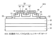
本実施形態は、第2の実施形態におけるGaN系ショットキーダイオード40の代わりに、図9に示される横型のGaN系ショットキーダイオード40Aを用いたものである。
このGaN系ショットキーダイオード40Aでは、n型GaN層44の表面の2箇所に凸部が形成されている。図5のGaN系ショットキーダイオード40と比較すると、n型GaN層44の凸部の数が1個から2個に増加している。そして、n型GaN層44の平坦部の表面及び2つの凸部の側面の上に、Al0.2Ga0.8N層46が形成されている。また、n型GaN層44の2つの凸部の上面上に、Ti電極48がそれぞれ形成されている。更に、これら2つのTi電極48上及びAl0.2Ga0.8N層46上に、Pt電極49が形成されている。
【0053】
従って、複合アノード電極50とカソード電極52との間に順方向バイアスを印加した際には、電流経路となるn型GaN層44aの凸部の数が増えた分だけ、第2の実施形態の場合よりも順方向電流が増大する。
なお、図9のGaN系ショットキーダイオード40Aの製造方法は、第2の実施形態におけるGaN系ショットキーダイオード40の場合と基本的に同様であるため、その説明は省略する。
【0054】
以上のように実施形態では、GaN系ショットキーダイオード40Aが、第2の実施形態におけるGaN系ショットキーダイオード40と同様の基本構造を有し、同様の特性を実現できることに加え、更にn型GaN層44の凸部の数が増加した分だけ順方向電流を増大させることができる。従って、このGaN系ショットキーダイオード40Aを、電力変換装置の電力変換回路であるインバータ回路又はコンバータ回路におけるパワーFET10(スイッチング素子)の保護素子として用いることにより、第2の実施形態の場合と同様又はそれ以上の効果を奏することができる。
【0055】
なお、本実施形態のGaN系ショットキーダイオード40Aにおいては、n型GaN層44の凸部の幅を第2の実施形態の場合よりも狭くして、より小さな逆方向バイアスでn型GaN層44の凸部の上面に形成される空乏層を通り抜ける逆方向リーク電流を阻止し、耐圧特性を向上することが可能になる。即ち、n型GaN層44の凸部の数を増加することと凸部の幅を狭くすることを組み合わせて、第2の実施形態において述べたトレードオフの関係になる2つの特性上の要求を両立することが可能になる。従って、n型GaN層44の凸部の数は、2つに限定される必要はなく、3つ以上であってもよい。以上のことは、後述する第5、第7、第9、第11及び第13の実施形態における保護素子としてのGaN系ショットキーダイオードについても同様である。
【0056】
(第4の実施形態)
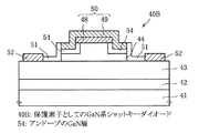
本実施形態は、第2の実施形態におけるGaN系ショットキーダイオード40の代わりに、図10に示される横型のGaN系ショットキーダイオード40Bを用いたものである。
このGaN系ショットキーダイオード40Bでは、図5のGaN系ショットキーダイオード40におけるAl0.2Ga0.8N層46の代わりに、厚さ50nmのアンドープのGaN層54が設けられている。即ち、n型GaN層44の凸部の側面とPt電極49との間に、GaN層54が介在している。従って、複合アノード電極50とカソード電極52との間に逆方向バイアスを印加する際には、n型GaN層44の凸部の側面に形成される空乏層の広がり方が、GaN層54の存在によってより大きくなる。
【0057】
なお、図10のGaN系ショットキーダイオード40Bの製造方法は、Al0.2Ga0.8N層46を形成する代わりにGaN層54を形成する点を除けば、第2の実施形態におけるGaN系ショットキーダイオード40の場合と基本的に同様であるため、その説明は省略する。
以上のように実施形態では、GaN系ショットキーダイオード40Bが、第2の実施形態におけるGaN系ショットキーダイオード40と同様の基本構造を有し、同様の特性を実現できることに加え、更にn型GaN層44の凸部の側面とPt電極49との間にアンドープのGaN層54を有するため、Pt電極49とのショットキー接触による空乏層の広がり方が更に大きくなり、良好な耐圧特性を更に向上できる。従って、このGaN系ショットキーダイオード40Bを、電力変換装置の電力変換回路であるインバータ回路又はコンバータ回路におけるパワーFET10(スイッチング素子)の保護素子として用いることにより、第2の実施形態の場合と同様又はそれ以上の効果を奏することができる。
【0058】
(第5の実施形態)
本実施形態は、第2の実施形態におけるGaN系ショットキーダイオード40の代わりに、図11に示される横型のGaN系ショットキーダイオード40Cを用いたものである。
このGaN系ショットキーダイオード40Cでは、第3の実施形態におけるGaN系ショットキーダイオード40Aと同様に、n型GaN層44の表面の2箇所に凸部が形成されている。また、第4の実施形態におけるGaN系ショットキーダイオード40Bと同様に、n型GaN層44の凸部の側面とPt電極49との間にGaN層54が形成されている。即ち、GaN系ショットキーダイオード40Cは、図9及び図10のGaN系ショットキーダイオード40A、40Bを組み合わせた構成となっている。
【0059】
なお、図11のGaN系ショットキーダイオード40Cの製造方法は、第3及び第4の実施形態におけるGaN系ショットキーダイオード40A、40Bの場合と基本的に同様であるため、その説明は省略する。
以上のように実施形態では、GaN系ショットキーダイオード40Cが、第3及び第4の実施形態におけるGaN系ショットキーダイオード40A、40Bを組み合わせた構成となっているため、これらGaN系ショットキーダイオード40A、40Bと同様の基本構造を有し、同様の特性を実現できる。従って、このGaN系ショットキーダイオード40Cを、電力変換装置の電力変換回路であるインバータ回路又はコンバータ回路におけるパワーFET10(スイッチング素子)の保護素子として用いることにより、第3又は第4の実施形態の場合と同様又はそれ以上の効果を奏することができる。
【0060】
(第6の実施形態)
本実施形態は、第2の実施形態におけるGaN系ショットキーダイオード40の代わりに、図12に示される横型のGaN系ショットキーダイオード40Dを用いたものである。
このGaN系ショットキーダイオード40Dでは、図5のGaN系ショットキーダイオード40におけるAl0.2Ga0.8N層46が形成されておらず、n型GaN層44の凸部の側面にPt電極49が直接にショットキー接触している。
なお、図12のGaN系ショットキーダイオード40Dの製造方法は、Al0. 2Ga0.8N層46を形成する工程を省略すれば、第2の実施形態におけるGaN系ショットキーダイオード40の場合と基本的に同様であるため、その説明は省略する。
【0061】
以上のように実施形態では、GaN系ショットキーダイオード40Dが、第2の実施形態におけるGaN系ショットキーダイオード40と同様の基本構造を有し、同様の特性を実現できることに加え、更にAl0.2Ga0.8N層がない分だけ構造及びその製造プロセスを簡略化することができる。従って、このGaN系ショットキーダイオード40Dを、電力変換装置の電力変換回路であるインバータ回路又はコンバータ回路におけるパワーFET10(スイッチング素子)の保護素子として用いることにより、第2の実施形態の場合と同様又はそれ以上の効果を奏することができる。
【0062】
(第7の実施形態)
本実施形態は、第2の実施形態におけるGaN系ショットキーダイオード40の代わりに、図13に示される横型のGaN系ショットキーダイオード40Eを用いたものである。
このGaN系ショットキーダイオード40Eでは、第3の実施形態におけるGaN系ショットキーダイオード40Aと同様に、n型GaN層44の表面の2箇所に凸部が形成されている。また、第6の実施形態におけるGaN系ショットキーダイオード40Dと同様に、n型GaN層44の凸部の側面にPt電極49が直接にショットキー接触している。即ち、GaN系ショットキーダイオード40Eは、図9及び図13のGaN系ショットキーダイオード40A、40Eを組み合わせた構成となっている。
【0063】
なお、図13のGaN系ショットキーダイオード40Eの製造方法は、図9及び図13のGaN系ショットキーダイオード40A、40Eの場合と基本的に同様であるため、その説明は省略する。
以上のように実施形態では、GaN系ショットキーダイオード40Eが、第3及び第6の実施形態におけるGaN系ショットキーダイオード40A、40Eを組み合わせた構成となっているため、これらGaN系ショットキーダイオード40A、40Bと同様の基本構造を有し、同様の特性を実現できる。従って、このGaN系ショットキーダイオード40Eを、電力変換装置の電力変換回路であるインバータ回路又はコンバータ回路におけるパワーFET10(スイッチング素子)の保護素子として用いることにより、第3又は第6の実施形態の場合と同様又はそれ以上の効果を奏することができる。
【0064】
(第8の実施形態)
本実施形態は、第2の実施形態におけるGaN系ショットキーダイオード40の代わりに、図14に示される縦型のGaN系ショットキーダイオード60を用いたものである。
このGaN系ショットキーダイオード60では、例えば導電性のn型SiC基板61上に、表面の一部が凸部形状に突出しているn型GaN層62が形成されている。n型GaN層62の不純物濃度は、2×1017cm-3程度の低濃度であり、その平坦部の厚さは500nm、凸部の幅及び高さはそれぞれ2000nm及び2000nmである。なお、n型GaN層62の不純物濃度は、2×1017cm-3程度に限定する必要はなく、2×1017cm-3以下であればよい。
【0065】
また、n型GaN層62の平坦部の表面及び凸部の両側面は、n型GaN層62よりもバンドギャップエネルギーの大きい厚さ30nmのアンドープのAl0.2Ga0.8N層63によって被覆されている。ここで、n型GaN層62とAl0.2Ga0.8N層63との接触部はヘテロ接合をなすため、そのヘテロ接合面近傍には、図中に破線で模式的に表した2次元電子ガスが発生する。
【0066】
また、n型GaN層62の凸部の上面にショットキー接触して、第1のアノード電極としてTi電極64が形成されている。なお、第1のアノード電極をなす材質は、Tiに限定されない。例えばWやAg等、1n型GaN層8に対して0.8eVより低いショットキーバリアを生じるものであればよい。
また、Ti電極64上及びAl0.2Ga0.8N層63上には、第2のアノード電極としてのPt電極65が形成されている。このPt電極65は、Ti電極64に電気的に接続すると共に、n型GaN層62の凸部の側面にAl0.2Ga0.8N層63を介してショットキー接触している。なお、第2のアノード電極をなす材質は、Ptに限定されない。例えばNiやPdやAu等、n型GaN層62に対して0.8eVより高いショットキーバリアを生じるものであればよい。
【0067】
そして、n型GaN層62の凸部の上面にショットキー接触しているTi電極64と、n型GaN層62の凸部の側面にAl0.2Ga0.8N層63を介してショットキー接触しているPt電極65とが互いに電気的に接続されて、複合アノード電極66を構成している。
また、Pt電極65、Al0.2Ga0.8N層63及びn型GaN層62の各側面、並びにn型SiC基板61の表面を被覆するSiO2 膜67が形成されている。また、n型SiC基板61の裏面にオーミック接触するTa−Si層からなるカソード電極68が形成されている。
【0068】
このようにGaN系ショットキーダイオード60は、第2の実施形態に係る横型のGaN系ショットキーダイオード40の絶縁性又は半絶縁性のサファイア基板41の代わりに、導電性のn型SiC基板61を用い、そのn型SiC基板61の裏面にカソード電極68を形成して、縦型構造としたものである。そして、横型構造と縦型構造の違いはあれ、n型GaN層62の凸部の上面にTi電極64がショットキー接触し、その凸部の側面にAl0.2Ga0.8N層63を介してPt電極65がショットキー接触し、これらTi電極64とPt電極65とから複合アノード電極66が構成されるという基本的な構造は、第2の実施形態におけるGaN系ショットキーダイオード60と同様である。
【0069】
次に、図14のGaN系ショットキーダイオード60の電流−電圧特性について説明する。
複合アノード電極66とカソード電極68との間に順方向バイアスを印加したところ、第2の実施形態の場合と略同様に、0.1〜0.3Vのオン電圧で、順方向電流が急激に増大する良好な立ち上りが観測された。また、複合アノード電極66とカソード電極68との間に逆方向バイアスを印加したところ、約500Vという大きな耐圧が観測された。このような良好な立ち上り特性と耐圧特性が得られた理由は、第2の実施形態におけるGaN系ショットキーダイオード60について述べた理由と同様であると考えられる。
【0070】
次に、図14のGaN系ショットキーダイオード60の製造方法の一例について、図15(a)〜(c)を用いて説明する。
先ず、導電性のn型SiC基板61上に、超真空成長装置を用いた例えばガスソースMBE法により、一連の結晶成長を行う。
即ち、原料ガスとして例えば分圧6.65×10⁻⁵PaのGaと分圧6.65×10⁻⁴PaのNH3 と分圧2×10⁻⁷PaのドーパントとしてのSiを用いて、2×1017cm-3程度の低不純物濃度のn型GaN層62を厚さ2500nmに成長させる(図15(a)参照)。
【0071】
次いで、第2の実施形態における図6(d)〜(e)及び図7(a)〜(d)に示す諸工程と同様の工程を行う。即ち、n型GaN層62を選択的にエッチング除去して、その表面の一部が突出した高さ2000nmの凸部を形成し、アンドープのAl0.2Ga0.8N層63を厚さ30nmに選択成長させる。続いて、n型GaN層62の凸部の上面にショットキー接触するTi電極64を形成し、n型GaN層62の凸部の側面にAl0.2Ga0.8N層63を介してショットキー接触するPt電極65を形成し、これらのTi電極64とPt電極65とから複合アノード電極66を構成する。続いて、SiO2 膜67を形成する(図15(b)参照)。
【0072】
次いで、n型SiC基板61の裏面にオーミック接触するTa−Si層からなるカソード電極68を形成する(図15(c)参照)。
このような一連の工程を経て、図14に示すGaN系ショットキーダイオード60を作製する。
なお、上記の製造方法の代わりに、第2の実施形態で図8(a)〜(d)を用いて説明した他の製造方法を適用することも可能である。
【0073】
以上のように実施形態では、GaN系ショットキーダイオード60が、横型構造と縦型構造の違いはあれ、第2の実施形態におけるGaN系ショットキーダイオード40と同様の基本的な構造を有し、同様の特性を実現できる。従って、このGaN系ショットキーダイオード60を、電力変換装置の電力変換回路であるインバータ回路又はコンバータ回路におけるパワーFET10(スイッチング素子)の保護素子として用いることにより、第2の実施形態の場合と同様の効果を奏することができる。
【0074】
(第9の実施形態)
本実施形態は、第8の実施形態におけるGaN系ショットキーダイオード60の代わりに、図16に示される縦型のGaN系ショットキーダイオード60Aを用いたものである。
このGaN系ショットキーダイオード60Aでは、図14のGaN系ショットキーダイオード60におけるn型GaN層62の凸部の数が1個から2個に増加している。別の観点から言えば、第3の実施形態のGaN系ショットキーダイオード40Aにおいて、サファイア基板41の代わりにn型SiC基板61を用い、そのn型SiC基板61の裏面にカソード電極68を形成して、縦型構造としたものである。
【0075】
なお、図16のGaN系ショットキーダイオード60Aの製造方法は、第3の実施形態におけるGaN系ショットキーダイオード60の場合と基本的に同様であるため、その説明は省略する。
以上のように実施形態では、GaN系ショットキーダイオード60Aが、第3の実施形態における横型のGaN系ショットキーダイオード40Aを縦型構造にしたものであるため、同様の基本構造を有し、同様の特性を実現できる。従って、このGaN系ショットキーダイオード60Aを、電力変換装置の電力変換回路であるインバータ回路又はコンバータ回路におけるパワーFET10(スイッチング素子)の保護素子として用いることにより、第3の実施形態の場合と同様の効果を奏することができる。
【0076】
(第10の実施形態)
本実施形態は、第8の実施形態におけるGaN系ショットキーダイオード60の代わりに、図17に示される縦型のGaN系ショットキーダイオード60Bを用いたものである。
このGaN系ショットキーダイオード60Bでは、図14のGaN系ショットキーダイオード60におけるAl0.2Ga0.8N層63の代わりに、厚さ50nmのアンドープのGaN層69が用いられている。別の観点から言えば、第4の実施形態のGaN系ショットキーダイオード40Bにおいて、サファイア基板41の代わりにn型SiC基板61を用い、そのn型SiC基板61の裏面にカソード電極68を形成して、縦型構造としたものである。
【0077】
なお、図17のGaN系ショットキーダイオード60Bの製造方法は、Al0.2Ga0.8N層63を形成する代わりにGaN層69を形成する点を除けば、第8の実施形態におけるGaN系ショットキーダイオード60の場合と基本的に同様であるため、その説明は省略する。
以上のように実施形態では、GaN系ショットキーダイオード60Bが、第4の実施形態における横型のGaN系ショットキーダイオード40Bを縦型構造にしたものであるため、同様の基本構造を有し、同様の特性を実現できる。従って、このGaN系ショットキーダイオード60Bを、電力変換装置の電力変換回路であるインバータ回路又はコンバータ回路におけるパワーFET10(スイッチング素子)の保護素子として用いることにより、第4の実施形態の場合と同様の効果を奏することができる。
【0078】
(第11の実施形態)
本実施形態は、第10の実施形態におけるGaN系ショットキーダイオード60Bの代わりに、図18に示される縦型のGaN系ショットキーダイオード60Cを用いたものである。
このGaN系ショットキーダイオード60Cでは、図17のGaN系ショットキーダイオード60Bにおけるn型GaN層62の凸部の数が1個から2個に増加している。別の観点から言えば、第5の実施形態のGaN系ショットキーダイオード40Cにおいて、サファイア基板41の代わりにn型SiC基板61を用い、そのn型SiC基板61の裏面にカソード電極68を形成して、縦型構造としたものである。
【0079】
なお、図18のGaN系ショットキーダイオード60Cの製造方法は、第10の実施形態におけるGaN系ショットキーダイオード60Bの場合と基本的に同様であるため、その説明は省略する。
以上のように実施形態では、GaN系ショットキーダイオード60Cが、第5の実施形態における横型のGaN系ショットキーダイオード40Cを縦型構造にしたものであるため、同様の基本構造を有し、同様の特性を実現できる。従って、このGaN系ショットキーダイオード60Cを、電力変換装置の電力変換回路であるインバータ回路又はコンバータ回路におけるパワーFET10(スイッチング素子)の保護素子として用いることにより、第5の実施形態の場合と同様の効果を奏することができる。
【0080】
(第12の実施形態)
本実施形態は、第8の実施形態におけるGaN系ショットキーダイオード60の代わりに、図19に示される縦型のGaN系ショットキーダイオード60Dを用いたものである。
このGaN系ショットキーダイオード60Dでは、図14のGaN系ショットキーダイオード60におけるAl0.2Ga0.8N層63が形成されておらず、n型GaN層62の凸部の側面にPt電極65が直接にショットキー接触しているものである。別の観点から言えば、第6の実施形態のGaN系ショットキーダイオード40Dにおいて、サファイア基板41の代わりにn型SiC基板61を用い、そのn型SiC基板61の裏面にカソード電極68を形成して、縦型構造としたものである。
【0081】
なお、図19のGaN系ショットキーダイオード60Dの製造方法は、Al0.2Ga0.8N層63を形成する工程を省略すれば、第8の実施形態におけるGaN系ショットキーダイオード60の場合と基本的に同様であるため、その説明は省略する。
以上のように実施形態では、GaN系ショットキーダイオード60Dが、第6の実施形態における横型のGaN系ショットキーダイオード40Dを縦型構造にしたものであるため、同様の基本構造を有し、同様の特性を実現できる。従って、このGaN系ショットキーダイオード60Dを、電力変換装置の電力変換回路であるインバータ回路又はコンバータ回路におけるパワーFET10(スイッチング素子)の保護素子として用いることにより、第6の実施形態の場合と同様の効果を奏することができる。
【0082】
(第13の実施形態)
本実施形態は、第12の実施形態におけるGaN系ショットキーダイオード60Dの代わりに、図20に示される縦型のGaN系ショットキーダイオード60Eを用いたものである。
このGaN系ショットキーダイオード60Eでは、図19のGaN系ショットキーダイオード60Dにおけるn型GaN層62の凸部の数が1個から2個に増加している。別の観点から言えば、第7の実施形態の図13のGaN系ショットキーダイオード40Eにおいて、サファイア基板41の代わりにn型SiC基板61を用い、そのn型SiC基板61の裏面にカソード電極68を形成して、縦型構造としたものである。
【0083】
なお、図20のGaN系ショットキーダイオード60Eの製造方法は、第12の実施形態におけるGaN系ショットキーダイオード60Dの場合と基本的に同様であるため、その説明は省略する。
以上のように実施形態では、GaN系ショットキーダイオード60Eが、第7の実施形態における横型のGaN系ショットキーダイオード40Eを縦型構造にしたものであるため、同様の基本構造を有し、同様の特性を実現できる。従って、このGaN系ショットキーダイオード60Eを、電力変換装置の電力変換回路であるインバータ回路又はコンバータ回路におけるパワーFET10(スイッチング素子)の保護素子として用いることにより、第7の実施形態の場合と同様の効果を奏することができる。
【0084】
(第14の実施形態)
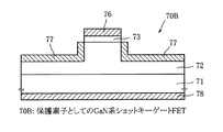
本実施形態は、第2の実施形態におけるGaN系ショットキーダイオード40の代わりに、図21に示される縦型のGaN系ショットキーゲートFET70を用いたものである。
このGaN系ショットキーゲートFET70では、例えば導電性のn型SiC基板71上に、表面の一部が凸部形状に突出しているn型GaN層72が形成されている。n型GaN層72の不純物濃度は、2×1017cm-3程度の低濃度であり、その平坦部の厚さは500nm、凸部の幅及び高さはそれぞれ2000nm及び2000nmである。なお、n型GaN層72の不純物濃度は2×1017cm-3程度に限定する必要はなく、2×1017cm-3以下であればよい。また、n型GaN層72の凸部の上面上には、厚さ50nm、5×1019cm-3程度の高不純物濃度のn+ 型GaN層73が積層されている。
【0085】
また、n型GaN層72の平坦部の表面及び凸部の両側面並びn+ 型GaN層73の側面は、n型GaN層72よりもバンドギャップエネルギーの大きい厚さ30nmのアンドープのAl0.2Ga0.8N層75によって被覆されている。ここで、n型GaN層72とAl0.2Ga0.8N層75との接触部はヘテロ接合をなすため、そのヘテロ接合面近傍には、図中に破線で模式的に表した2次元電子ガスが発生する。
【0086】
なお、後に説明するように、n型GaN層72の凸部は、GaN系ショットキーゲートFET70のドレイン電流ID が縦方向に流れるチャネル領域である。従って、このチャネル領域をドレイン電流ID が流れる際に、この2次元電子ガスがキャリアとしてに寄与する。即ち、一種の縦型のHEMT(High Electron Mobility Transistor ;高電子移動度トランジスタ)構造となっている。
【0087】
また、n+ 型GaN層73上に、Ta−Si層からなるソース電極76が形成されている。即ち、ソース電極76が、n+ 型GaN層73を介してn型GaN層72の凸部の上面にオーミック接触している。また、n型GaN層72の凸部の側面にAl0.2Ga0.8N層75を介してショットキー接触しているPt層からなるショットキーゲート電極77が形成されている。なお、ショットキーゲート電極77をなす材質は、Ptに限定されない。例えばTi、Ni、W、Ag、Pd、Au等、n型GaN層72に対してショットキーバリアを生じるものであればよいが、より高いショットキーバリアを生じる金属が好適である。また、n型SiC基板71の裏面にオーミック接触するTa−Si層からなるドレイン電極78が形成されている。
【0088】
次に、図21のGaN系ショットキーゲートFET70の電流−電圧特性について説明する。
n型GaN層72の凸部の側面には、Al0.2Ga0.8N層75を介してショットキーゲート電極77が形成されているため、このショットキーゲート電極77に印加するゲート電圧VG が、VG =0の場合であっても、n型GaN層72の凸部の両側面には空乏層が形成されている。この状態で、ソース電極76とドレイン電極78との間に、所定のドレイン電圧VD を印加すると、ドレイン電流ID はn型GaN層72の凸部の両側面の空乏層に挟まれた領域をチャネルとして縦方向に流れる。ドレイン電圧VD を増大すると、チャネルの幅が増大して、ドレイン電流ID も増大する。
【0089】
また、ゲート電圧VG の大きさを増減すると、n型GaN層72の凸部の両側面の空乏層の広がりが大きくなったり小さくなったりして、2方向から広がる空乏層に挟まれたチャネルの幅が変化する。このため、ゲート電圧VG によってチャネルの幅が制御され、そこを流れるドレイン電流ID が制御される。
このとき、n型GaN層72とAl0.2Ga0.8N層75とのヘテロ接合面近傍に発生する2次元電子ガスが、キャリアとしてドレイン電流ID に寄与するため、小さなドレイン電圧VD でドレイン電流ID が急速に立ち上る良好な立ち上り特性が得られる。
【0090】
また、ショットキーゲート電極77とn型GaN層72の凸部の側面との間には、n型GaN層72よりもバンドギャップエネルギーが大きなアンドープのAl0.2Ga0.8N層75が介在しているため、小さなゲート電圧VG でも空乏層は大きく広がる。その結果、ゲート電圧VG によるドレイン電流ID の制御性が向上する。
【0091】
次に、図21のGaN系ショットキーゲートFET70の製造方法の一例について、図22(a)〜(d)及び図23(a)〜(c)を用いて説明する。
先ず、導電性のn型SiC基板71上に、超真空成長装置を用いた例えばガスソースMBE法により、一連の結晶成長を行う。
即ち、原料ガスとして例えば分圧1.33×10⁻⁵PaのGaと分圧6.65×10⁻⁴PaのNH3 と分圧2×10⁻⁷PaのドーパントとしてのSiを用いて、2×1017cm-3程度の低不純物濃度のn型GaN層72を厚さ2500nmに成長させる。連続して、例えば分圧1.33×10⁻⁵PaのGaと分圧6.65×10⁻⁴PaのNH3 と分圧1.33×10⁻⁶PaのドーパントとしてのSiを用いて、5×1019cm-3程度の高不純物濃度のn+ 型GaN層73を厚さ50nmに成長させる(図22(a)参照)。
【0092】
次いで、例えばプラズマCVD法により、n+ 型GaN層73上にSiO2 膜を形成する。続いて、例えばBHFを用いたウエットエッチング法又はCF4 を用いたドライエッチング法により、SiO2 膜をパターニングして、例えば幅2μmをもつSiO2 パターン74を形成する(図22(b)参照)。
次いで、例えばメタン系ガスを用いたECRプラズマエッチング法又はRIBE法により、SiO2 パターン74をマスクとしてn+ 型GaN層73及びn型GaN層72を選択的にエッチング除去する。こうして、n型GaN層44の表面の一部が突出した高さ2000nm、幅2000nmの凸部を形成すると共に、その凸部の上面上にn+ 型GaN層73を残存させる(図22(c)参照)。
【0093】
次いで、SiO2 パターン74をマスクとし、例えば分圧6.65×10⁻⁵PaのGaと分圧2.66×10⁻⁵PaのAlと分圧6.65×10⁻⁴PaのNH3 を原料ガスとして、アンドープのAl0.2Ga0.8N層75を厚さ30nmに選択成長させる。こうして、n型GaN層72の平坦部の表面及び凸部の側面並びにn+ 型GaN層73の側面をAl0.2Ga0.8N層75によって被覆する(図22(d)参照)。
【0094】
次いで、SiO2 パターン74を除去する。続いて、リフトオフ法により、n+ 型GaN層73の上面上にTa−Si層を選択的に形成する。こうして、n型GaN層44の凸部の上面にn+ 型GaN層73を介してオーミック接触するTa−Si層からなるソース電極76を形成する(図23(a)参照)。
次いで、図23(a)に示す工程と同様にして、リフトオフ法により、Al0.2Ga0.8N層75上に、Pt層を選択的に形成する。こうして、n型GaN層72の凸部の側面にAl0.2Ga0.8N層75を介してショットキー接触するPt層からなるショットキーゲート電極77を形成する(図23(b)参照)。
【0095】
次いで、n型SiC基板71の裏面にオーミック接触するTa−Si層からなるドレイン電極78を形成する(図23(c)参照)。
このような一連の工程を経て、図21に示すGaN系ショットキーゲートFET70を作製する。
以上のように実施形態では、GaN系ショットキーゲートFET70が、チャネル領域をなすn型GaN層72の凸部の上面にソース電極76がオーミック接触し、その凸部の側面にショットキーゲート電極77がショットキー接触し、n型SiC基板71の裏面にドレイン電極78がオーミック接触している基本構造を有しており、n型GaN層72の凸部の側面とショットキーゲート電極77との間にバンドギャップエネルギーの大きなアンドープのAl0.2Ga0.8N層75を有しているため、n型GaN層72とAl0.2Ga0.8N層75とのヘテロ接合面近傍に発生する2次元電子ガスがドレイン電流ID に寄与し、ドレイン電流ID の良好な立ち上り特性が得られる。また、ショットキーゲート電極77とのショットキー接触による空乏層の広がり方が更に大きくなり、ゲート電圧VG によるドレイン電流ID の制御性を向上させることができる。
【0096】
従って、このGaN系ショットキーゲートFET70を、電力変換装置の電力変換回路であるインバータ回路又はコンバータ回路におけるパワーFET10(スイッチング素子)の保護素子として用いることにより、損失を低下させ、高いインバータ効率又はコンバータ効率を達成することが可能になり、電力変換装置の高効率化を実現できる。
【0097】
(第15の実施形態)
本実施形態は、第14の実施形態におけるGaN系ショットキーゲートFET70の代わりに、図24に示される縦型のGaN系ショットキーゲートFET70Aを用いたものである。
【0098】
このGaN系ショットキーゲートFET70Aでは、図21のGaN系ショットキーゲートFET70におけるAl0.2Ga0.8N層75の代わりに、厚さ50nmのアンドープのGaN層79が設けられている。即ち、n型GaN層72の凸部の側面とショットキーゲート電極77との間に、GaN層79が介在している。
【0099】
なお、図24のGaN系ショットキーゲートFET70Aの製造方法は、Al0.2Ga0.8N層75を形成する代わりにGaN層79を形成する点を除けば、第14の実施形態におけるGaN系ショットキーゲートFET70の場合と基本的に同様であるため、その説明は省略する。
以上のように実施形態では、GaN系ショットキーゲートFET70Aが、第14の実施形態におけるGaN系ショットキーゲートFET70と同様の基本構造を有し、同様の特性を実現できることに加え、更にn型GaN層72の凸部の側面とショットキーゲート電極77との間にアンドープのGaN層79を有するため、ショットキーゲート電極77とのショットキー接触による空乏層の広がり方が更に大きくなり、ゲート電圧VG によるドレイン電流ID の制御性を向上させることができる。従って、このGaN系ショットキーゲートFET70Aを、電力変換装置の電力変換回路であるインバータ回路又はコンバータ回路におけるパワーFET10(スイッチング素子)の保護素子として用いることにより、第14の実施形態の場合と同様又はそれ以上の効果を奏することができる。
【0100】
(第16の実施形態)
本実施形態は、第14の実施形態におけるGaN系ショットキーゲートFET70の代わりに、図25に示される縦型のGaN系ショットキーゲートFET70Bを用いたものである。
このGaN系ショットキーゲートFET70Bでは、図21のGaN系ショットキーゲートFET70におけるAl0.2Ga0.8N層75が形成されておらず、n型GaN層72の凸部の側面にショットキーゲート電極77が直接にショットキー接触している。
なお、図25のGaN系ショットキーゲートFET70Bの製造方法は、Al0.2Ga0.8N層75を形成する工程を省略すれば、第14の実施形態におけるGaN系ショットキーゲートFET70の場合と基本的に同様であるため、その説明は省略する。
【0101】
以上のように実施形態では、GaN系ショットキーゲートFET70Bが、第14の実施形態におけるGaN系ショットキーゲートFET70と同様の基本構造を有し、同様の特性を実現できる。従って、このGaN系ショットキーゲートFET70Bを、電力変換装置の電力変換回路であるインバータ回路又はコンバータ回路におけるパワーFET10(スイッチング素子)の保護素子として用いることにより、第14の実施形態の場合と同様の効果を奏することができる。
【0102】
なお、第2〜第16の実施形態では、n型GaN層44、62、72の凸部の幅は2000nmとなっているが、この例示した値に限定されるものではない。この凸部の幅は、例えば5nm〜10μmの範囲内にあればよく、好ましくは10nm〜5μmの範囲内に、更に好ましくは50nm〜3μmの範囲内にあればよい。
【0103】
また、第2〜第16の実施形態では、GaN系のIII-V族窒化物半導体層を結晶成長する際にガスソースMBE法を用いているが、その製法はガスソースMBE法に限定されるものではなく、例えばMOCVD(Metal Organic Chemical Vapor Deposition ;有機金属化学気相成長)法やハイドライド気相成長法等を代わりに用いてもよい。
【0104】
また、第8〜第16の実施形態では、導電性のn型SiC基板61、71を用いているが、例えばSiC、Si、GaN、AlN、GaAs、GaP等からなる導電性の半導体基板を代わりに用いてもよい。
また、第1〜第3、第8、第9及び第14の実施形態では、2次元電子ガスを発生させるヘテロ接合構造として、GaN23層とAlGaN層24、n型GaN層44とAlGaN層46、n型GaN層62とAlGaN層63、n型GaN層72とAlGaN層75の組み合わせによるGaN/AlGaN接合を用いているが、例えばInGaN、AlInGaN、AlInGaNP、AlGaN、AlGaN等のIII-V族窒化物半導体層を組み合わせたヘテロ接合を代わりに用いてもよい。また、ヘテロ接合を用いずに、上記のAlGaN層の代わりに、Siをドープしたn型GaN層を用いてもよい。
【0105】
(第17の実施形態)
本実施形態は、図26(a)に示されるように、第1の実施形態におけるスイッチング素子であるパワーFET10として、GaN系MESFET10Aを用い、このGaN系MESFET10Aに、保護素子としてのGaN系ショットキーダイオード20Aが内蔵されているものである。具体的には、GaN系MESFET10Aのソース・ドレイン間に、横型のGaN系ショットキーダイオード20Aが接続されている。
【0106】
また、図26(b)に示されるように、これらのGaN系MESFET10A及びGaN系ショットキーダイオード20Aは、同一基板上に集積されている。即ち、例えばサファイア基板21上に、GaNバッファ層22、アンドープのGaN層23及びアンドープのAlGaN層24が順に積層して形成されている。また、GaN層23とAlGaN層24とのヘテロ接合部に接続して、2つのn型GaN層26がGaN層23上に形成されている。
【0107】
更に、2つのn型GaN層26上にそれぞれオーミック接触して、ソース電極とカソード電極とを兼用する電極(以下、単に「ソース・カソード兼用電極」という)27a及びドレイン電極27bが形成されている。また、2つのn型GaN層26に挟まれたAlGaN層24上にショットキー接触して、ゲート電極28aが形成されている。また、ソース・カソード兼用電極27aを間に挟んでゲート電極28aの反対側のAlGaN層24上にショットキー接触して、アノード電極28bが形成されている。
【0108】
即ち、本実施形態は、スイッチング素子(パワーFET10)としてのGaN系MESFET10A及びその保護素子としてのGaN系ショットキーダイオード20を同一基板上に集積したものである。
次に、図26(b)のGaN系MESFET10A及びGaN系ショットキーダイオード20Aの製造方法の一例について、図27(a)〜(d)を用いて説明する。
【0109】
先ず、半絶縁性のサファイア基板21上に、厚さ5nmのGaNバッファ層22、厚さ3000nmのアンドープのGaN層23、厚さ30nmのアンドープのAlGaN層24を順に成長させる。こうして、GaN層23とAlGaN層24とのヘテロ接合構造を形成する(図27(a)参照)。
次いで、AlGaN層24上に形成したSiO2膜を選択的にエッチング除去し、2箇所に開口部を有するSiO2パターン25を形成した後、このSiO2パターン25をマスクとしてAlGaN層24及びGaN層23の一部を順に選択的にエッチング除去し、GaN層23表面を露出させる(図27(b)参照)。
【0110】
次いで、これら2箇所の露出させたGaN層23上にそれぞれ、5×1019cm-3程度の高濃度にSiを添加したn型GaN層26を選択的に成長させる(図27(c)参照)。
次いで、これら2つのn型GaN層26にそれぞれオーミック接触するTaSi/Au積層構造のソース・カソード兼用電極27a及びドレイン電極27bを形成する。また、これら2つのn型GaN層26に挟まれたAlGaN層24上にショットキー接触するTi/WSi/Au積層構造のゲート電極28aを形成すると共に、ソース・カソード兼用電極27aを間に挟んでゲート電極28aの反対側のAlGaN層24上にショットキー接触するTi/WSi/Au積層構造のアノード電極28bを形成する(図27(c)参照)。
【0111】
このような一連の工程を経て、図26(b)に示すGaN系MESFET10A及びGaN系ショットキーダイオード20Aが同一基板上に集積されているGaN系半導体装置を作製する。
以上のように本実施形態では、GaN系MESFET10A及びGaN系ショットキーダイオード20Aが、共通の材料を用いた共通の工程によって同時的に形成される。即ち、GaN系MESFET10Aを作製する工程で、選択的エッチングや選択的結晶成長のためのマスクパターンに修正を加えるだけで、何ら工程を煩雑化したり増加したりする必要はない。従って、スイッチング素子とGaN系ショットキーダイオードをそれぞれ各別の電子部品として作製し、接続する場合に較べて、製造コストの低減を実現するのみならず、集積化による部品の小型化を達成し、延いては電力変換装置の小型化を実現することができる。
【0112】
また、GaN系ショットキーダイオード20Aが、同一基板上に形成されているGaN系MESFET10Aの保護素子として機能する。そして、このGaN系半導体装置を電力変換装置の電力変換回路であるインバータ回路又はコンバータ回路のスイッチング素子に用いる場合、その構成は第1の実施形態の図3又は図4(a)〜(d)に例示される場合と同様であり、その作用効果も上記第1の実施形態において述べたものと同様である。
【0113】
但し、この電力変換装置の場合、前述した高いインバータ効率又はコンバータ効率の達成に伴い、GaN系ショットキーダイオード20Aを内蔵したGaN系MESFET10Aは、同一性能の従来のpn接合構造のツェナーダイオードを内蔵したSi系MOSFETと比較して、そのチップ面積を縮小することが可能になる。また、インバータ回路又はコンバータ回路からなる電力変換回路に使用する個数も大幅に低減することが可能になる。従って、電力変換装置用の大幅な小型化を実現することができる。
【0114】
因みに、電力変換装置用のスイッチング素子として、図26(a)、(b)に示されるようなGaN系ショットキーダイオード20Aを内蔵したGaN系MESFET10Aを試作したところ、同一性能の従来のpn接合構造のツェナーダイオードを内蔵したSi系MOSFETの場合に較べて、チップ面積を例えば1cm2から16mm2に縮小することができた。また、上記の試作したスイッチング素子を電力変換装置の電力変換回路としてのインバータ回路に組み込んだ場合には、必要とするチップ数を従来の場合の半分以下に低減することができた。また、電力変換回路としてのコンバータ回路に組み込んだ場合には、必要とするチップ数を従来の場合の例えば32個から8個に低減することができた。
【0115】
なお、本実施形態では、スイッチング素子(パワーFET10)としてGaN系MESFET10Aと第1の実施形態における保護素子としてのGaN系ショットキーダイオード20とを同一基板上に集積した場合について説明したが、スイッチング素子とその保護素子との集積は、この組合せに限定されるものではない。例えばGaN系MESFET10Aと第2〜第7の実施形態における保護素子としてのGaN系ショットキーダイオード40、40A〜40Eの何れかとを同一基板上に集積することも可能である。
【0116】
(第18の実施形態)
本実施形態は、図28(a)に示されるように、第1の実施形態におけるパワーFET10の代わりに、IGBT80を用いたものである。具体的には、スイッチング素子としてのIGBT80のエミッタ・コレクタ間に、保護素子としてのGaN系ショットキーダイオード20が接続されている。
【0117】
ここで、図28(b)に示されるGaN系ショットキーダイオード20は、第1の実施形態の図1(b)に示されるものと同一であり、その構造及びその製造方法についての説明は省略する。
また、図28(a)に示したIGBT80及びGaN系ショットキーダイオード20を電力変換装置の電力変換回路であるインバータ回路又はコンバータ回路に用いる場合には、第1の実施形態の図3又は図4(a)〜(d)に例示される回路図において、パワーFET10をIGBT80によって置換すればよく、その基本的な回路構成は同一である。このため、この場合の電力変換装置の電力変換回路であるインバータ回路又はコンバータ回路の図示は省略する。
【0118】
以上のように本実施形態では、スイッチング素子であるIGBT80の保護素子として用いられるGaN系ショットキーダイオード20が、600Vを超える耐圧を有していることから、IGBT80は少なくとも500V以上の高耐圧での例えば100A以上の大電流動作が容易に可能になる。また、第1の実施形態の場合と同様、動作瞬時の突入電流又はサージ電圧が印加する場合であっても、GaN系ショットキーダイオード20が保護素子として機能する前にIGBT80が発熱により破壊されることを防止することが可能になるため、安定動作が保証され、電力変換装置の信頼性を高めることができる。
【0119】
なお、本実施形態では、スイッチング素子としてのIGBT80に第1の実施形態における保護素子としてのGaN系ショットキーダイオード20を組み合わせた場合について説明したが、例えばIGBT80に第2〜第16の実施形態における保護素子としてのGaN系ショットキーダイオード40、40A〜40E、60、60A〜60E又はGaN系ショットキーゲートFET70、70A、70Bの何れかを組み合わせることも可能である。
【0120】
【発明の効果】
以上詳細に説明したように、本発明によれば、電力変換装置の電力変換回路を構成するスイッチング素子の保護素子として、オン電圧が1V以下と低く、耐圧が300V以上と高いGaN系ショットキーダイオード又はGaN系FETが用いられることにより、スイッチング素子の低オン電圧動作が容易に可能になる。このため、電力変換回路として例えばインバータ回路又はコンバータ回路を用いる場合、損失を低下させて、高いインバータ効率又はコンバータ効率を達成することが可能になり、電力変換装置の高効率化を実現することができる。また、動作瞬時の突入電流又はサージ電圧が印加する場合であっても、高耐圧のGaN系ショットキーダイオードが保護素子として機能するため、スイッチング素子の安定動作が保証され、電力変換装置の信頼性を高めることができる。更に、スイッチング素子の高耐圧での大電流動作が容易に可能になる。
【0121】
また、電力変換装置の電力変換回路を構成するスイッチング素子としてのGaN系FETとその保護素子としてのGaN系ショットキーダイオードとが同一の基板上に集積されていることにより、従来のpn接合構造のツェナーダイオードを内蔵したSi系MOSFETと比較して、そのチップ面積を縮小することが可能になると共に、電力変換回路に使用する個数も大幅に低減することが可能になる。このため、電力変換装置用の大幅な小型化を実現することができる。
【図面の簡単な説明】
【図1】(a)は本発明の第1の実施形態に係るスイッチング素子としてのパワーFET及びその保護素子としてのGaN系ショットキーダイオードを示す回路図であり、(b)はそのGaN系ショットキーダイオードを示す概略断面図である。
【図2】(a)〜(d)はそれぞれ図1(b)に示されるGaN系ショットキーダイオードの製造方法を説明するための工程断面図である。
【図3】図1(a)、(b)に示されるパワーFET及びGaN系ショットキーダイオードを用いたインバータ回路を有する電力変換装置を示す回路図である。
【図4】(a)〜(d)はそれぞれ図1(a)、(b)に示されるパワーFET及びGaN系ショットキーダイオードを用いたコンバータ回路を有する電力変換装置を示す回路図である。
【図5】本発明の第2の実施形態に係る横型のGaN系ショットキーダイオードを示す概略断面図である。
【図6】図5のGaN系ショットキーダイオードの製造方法の一例を説明するための工程断面図(その1)である。
【図7】図5のGaN系ショットキーダイオードの製造方法の一例を説明するための工程断面図(その2)である。
【図8】図5のGaN系ショットキーダイオードの製造方法の他の例を説明するための工程断面図である。
【図9】本発明の第3の実施形態に係る横型のGaN系ショットキーダイオードを示す概略断面図である。
【図10】本発明の第4の実施形態に係る横型のGaN系ショットキーダイオードを示す概略断面図である。
【図11】本発明の第5の実施形態に係る横型のGaN系ショットキーダイオードを示す概略断面図である。
【図12】本発明の第6の実施形態に係る横型のGaN系ショットキーダイオードを示す概略断面図である。
【図13】本発明の第7の実施形態に係る横型のGaN系ショットキーダイオードを示す概略断面図である。
【図14】本発明の第8の実施形態に係る縦型のGaN系ショットキーダイオードを示す概略断面図である。
【図15】図14のGaN系ショットキーダイオードの製造方法の一例を説明するための工程断面図である。
【図16】本発明の第9の実施形態に係る縦型のGaN系ショットキーダイオードを示す概略断面図である。
【図17】本発明の第10の実施形態に係る縦型のGaN系ショットキーダイオードを示す概略断面図である。
【図18】本発明の第11の実施形態に係る縦型のGaN系ショットキーダイオードを示す概略断面図である。
【図19】本発明の第12の実施形態に係る縦型のGaN系ショットキーダイオードを示す概略断面図である。
【図20】本発明の第13の実施形態に係る縦型のGaN系ショットキーダイオードを示す概略断面図である。
【図21】本発明の第14の実施形態に係る縦型のGaN系ショットキーゲートFETを示す概略断面図である。
【図22】図21のGaN系ショットキーゲートFETの製造方法の一例を説明するための工程断面図(その1)である。
【図23】図21のGaN系ショットキーゲートFETの製造方法の一例を説明するための工程断面図(その2)である。
【図24】本発明の第15の実施形態に係る縦型のGaN系ショットキーゲートFETを示す概略断面図である。
【図25】本発明の第16の実施形態に係る縦型のGaN系ショットキーゲートFETを示す概略断面図である。
【図26】(a)は本発明の第17の実施形態に係るスイッチング素子としてのGaN系MESFET及びその保護素子としてのGaN系ショットキーダイオードを示す回路図であり、(b)はそのGaN系ショットキーダイオードを内蔵しているGaN系MESFETを示す概略断面図である。
【図27】(a)〜(d)はそれぞれ図26(b)に示されるGaN系ショットキーダイオードを内蔵しているGaN系MESFETの製造方法を説明するための工程断面図である。
【図28】(a)は本発明の第18の実施形態に係るスイッチング素子としてのIGBT及びその保護素子としてのGaN系ショットキーダイオードを示す回路図であり、(b)はそのGaN系ショットキーダイオードを示す概略断面図である。
【符号の説明】
10 スイッチング素子としてのパワーFET
10A スイッチング素子としてのGaN系MESFET
20、20A、40、40A〜40E、60、60A〜60E 保護素子としてのGaN系ショットキーダイオード
21、41 絶縁性又は半絶縁性のサファイア基板
22、42 GaNバッファ層
23、54、69、79 アンドープのGaN層
24 アンドープのAlGaN層
26、44、72 n型GaN層
27、52 カソード電極
27a ソース・カソード兼用電極
27b、78 ドレイン電極
28、28b アノード電極
28a ゲート電極
30 電力変換装置
31 交流電源
32 整流回路
34 DC−ACインバータ回路
34a、34b、…、34d DC−DCコンバータ回路
43、73 n+ 型GaN層
46、63、75 アンドープのAl0.2Ga0.8N層
48 第1のアノード電極としてのTi電極
49 第2のアノード電極としてのPt電極
50 複合アノード電極
61 導電性のn型SiC基板
62 n型GaN層
64 第1のアノード電極としてのTi電極
65 第2のアノード電極としてのPt電極
66 複合アノード電極
68 カソード電極
70、70A、70B 保護素子としてのGaN系ショットキーゲートFET
71 導電性のn型SiC基板
76 ソース電極
77 ショットキーゲート電極
80 スイッチング素子としてのIGBT[0001]
BACKGROUND OF THE INVENTION
The present invention relates to a power conversion device having a power conversion circuit and a GaN-based semiconductor device used for the power conversion circuit.
[0002]
[Prior art]
Since a switching element incorporated in a power conversion circuit of a power conversion device needs to handle power of several watts or more, conventionally, a bipolar transistor has been mainly used. However, FETs (Field Effect Transistors) that handle high power have been developed since then, and power MOSFETs (Metal Oxide Semiconductor FETs) have come to be widely used. Alternatively, an IGBT (Insulated Gate Bipolar Transistor) that is a composite of a bipolar transistor and a MOSFET can operate at a high voltage at a high speed like a bipolar transistor, and has a low on-resistance like a MOSFET. Therefore, it is used as a switching element.
[0003]
By the way, in such a power MOSFET or the like, it is necessary to incorporate a protective element in order to remove the parasitic bipolar transistor effect or to prevent element destruction due to application of an instantaneous rush current or surge voltage. For example, in the most common Si-based MOSFET, a Zener diode using a pn junction is usually incorporated as a protection element.
[0004]
[Problems to be solved by the invention]
However, the Zener diode having the pn junction structure used as the conventional protection element described above has an on-resistance of 10 mΩcm.2Since the on-voltage at the rising in the forward direction is as high as about 1.2 to 1.5V, the breakdown voltage is as low as about 100V.
For this reason, when a MOSFET having a low on-voltage is used as a switching element constituting the power conversion circuit of the power conversion device, the following problems occur when the Zener diode having the pn junction structure described above is incorporated as the protection element. It was.
[0005]
In other words, since the protection device has a low withstand voltage and a high on-voltage, it cannot sufficiently withstand the inrush current or surge voltage of the MOSFET, or heat is generated when a surge voltage is applied, and the protection device The MOSFET was destroyed before it worked, so that the stable operation of the power conversion device could not be guaranteed, and the reliability was lowered. Further, the low on-voltage operation of the MOSFET cannot be performed, resulting in a high loss, and the efficiency of the power converter is lowered.
[0006]
On the other hand, GaN-based FETs are known to have a high withstand voltage and are capable of high-temperature operation and large-current operation, and research and development of various devices using GaN-based semiconductor materials are underway. However, up to now, there has been no known case where a power conversion device is configured by incorporating a GaN-based semiconductor device.
The present invention has been made in consideration of the above-described conventional problems, and by utilizing the characteristics of a GaN-based semiconductor material, a power converter having high reliability and high efficiency that guarantees stable operation, and the same An object of the present invention is to provide a GaN-based semiconductor device as a component used for realizing the above.
[0007]
[Means for Solving the Problems]
In order to achieve the above object, in the present invention, a power conversion device having a power conversion circuit, wherein a GaN-based Schottky diode or a GaN-based FET is used as a protective element of a switching element constituting the power conversion circuit. The power converter characterized by being provided is provided.
[0008]
In the present invention, the GaN-based Schottky diode is used as a protective element of a switching element constituting a power conversion circuit of a power conversion device, and has an on-voltage of 1 V or less and a withstand voltage of 300 V or more. A GaN-based semiconductor device is provided.
In the present invention, the GaN-based FET is used as a protective element of a switching element constituting a power conversion circuit of a power conversion device, and is a GaN-based FET having an on-voltage of 1 V or less and a withstand voltage of 300 V or more. A semiconductor device is provided.
[0009]
DETAILED DESCRIPTION OF THE INVENTION
Hereinafter, embodiments of the present invention will be described with reference to the accompanying drawings. In addition, the same code | symbol is attached | subjected to the component which is common in each embodiment, and description is abbreviate | omitted. (First embodiment)
In the present embodiment, as shown in FIG. 1A, a
[0010]
Here, the power FET 10 may be a Si-based MOSFET, a GaN-based MISFET (Metal Insulator Semiconductor FET), or a GaN-based MESFET (Metal Semiconductor FET).
The GaN-based Schottky
[0011]
Next, an example of a method for manufacturing the GaN-based Schottky
First, a series of crystal growth is performed on the
[0012]
That is, a partial pressure of 6.65 × 10 as a source gas-FivePa Ga (gallium) and radicalized partial pressure 4.0 × 10-FourThe GaN
[0013]
In this series of crystal growth, a MOCVD (Metal Organic Chemical Vapor Deposition) method, a halide vapor phase growth method, or the like may be used instead of the gas source MBE method.
Next, the first intermediate is once taken out from the ultra-vacuum growth apparatus, and is then formed on the AlGaN
[0014]
Subsequently, for example, an ECR (Electron Cyclotron Resonance) plasma etching method using a methane-based gas or a reactive ion beam etching (RIBE) method is used to form SiO.2Using the
[0015]
The second intermediate is then loaded again into the ultra-vacuum growth apparatus and then SiO 22Using the
[0016]
Next, after removing the third intermediate from the ultra-vacuum growth apparatus, SiO 32The
[0017]
Similarly, SiO2After selectively removing the film by etching and opening a contact hole exposing the
Through such a series of steps, the GaN-based
[0018]
Incidentally, when the inventors made a prototype of a GaN-based Schottky diode as shown in FIG. 1B according to the above manufacturing method and measured its characteristics, the following results were obtained. That is, the breakdown voltage of the GaN-based Schottky diode exceeded 600V. The on-resistance is 24 mΩcm2The forward voltage rose from around 0.3V. Moreover, the electric current was able to flow up to 100A.
[0019]
Next, a power conversion device having a power conversion circuit using the
In general, an inverter circuit or a converter circuit is used as the power conversion circuit of the power conversion device. And the inverter circuit or converter circuit actually used as a power converter circuit has a very versatile circuit configuration due to various requirements for its control function. Therefore, here, an example of a power converter having an inverter circuit is shown using FIG. 3, and several examples of the power converter having a converter circuit are shown using FIGS. 4 (a) to 4 (d).
[0020]
As shown in FIG. 3, the power conversion device 30 includes an AC power supply 31 having a frequency of 50 Hz or 60 Hz and a voltage of 100 V, a
[0021]
As shown in FIGS. 4A to 4D, the power conversion device includes (a) Buck circuit (step-down type), (b) Boost circuit (step-up type), and (c) Boost-Buck circuit (step-up / step-down type). And (d) DC-
[0022]
As described above, in the present embodiment, the GaN-based
[0023]
Further, even when an instantaneous rush current or surge voltage is applied, the GaN-based
[0024]
Note that the GaN-based
[0025]
(Second Embodiment)
In the present embodiment, a lateral GaN-based
In the GaN-based
[0026]
Further, the surface of the flat portion and the side surface of the convex portion of the n-
[0027]
Further, a Ti (titanium)
[0028]
Also,
[0029]
Then, the
Also,
[0030]
Next, the current-voltage characteristics of the GaN-based
When a forward bias was applied between the
[0031]
The on-voltage required for rising when a forward bias is applied between the Schottky-contacted Ti electrode and the n-type GaN layer is generally about 0.3 to 0.5V. In addition, the on-voltage required for rising when a forward bias is applied between the Pt electrode and the n-type GaN layer in Schottky contact is generally about 1.0 to 1.5V.
[0032]
In the GaN-based
[0033]
When a reverse bias was applied between the
When a reverse bias is applied between the Schottky contact Ti electrode and the n-type GaN layer, it is generally 10 V at −10V.-6-10-FiveA reverse leakage current of about A is generated. Further, when a reverse bias is applied between the Schottky contact Pt electrode and the n-type GaN layer, the reverse leakage current is much smaller than in the above case, and a breakdown voltage of about 500 V is obtained.
[0034]
When a reverse bias is applied to the GaN-based
At the stage where the reverse bias is smaller than −10 V, there is almost no reverse leakage current passing through the depletion layer formed on the side surface of the convex portion of the
[0035]
As a result, when the reverse bias increases and reaches about −10 V, the depletion layers extending from both side surfaces of the convex portion of the
[0036]
Next, an example of a manufacturing method of the GaN-based
First, a series of crystal growth is performed on the
That is, a partial pressure of 6.65 × 10 as a source gas-FivePartial pressure 4.0 × 10 radicalized with Pa Ga-FourUsing N of Pa, the
[0037]
Further continuously, for example, a partial pressure of 1.33 × 10-FourPa Ga and partial pressure 6 × 10-FourNH of PaThreeAnd
[0038]
Next, after the first intermediate is once taken out from the ultra-vacuum growth apparatus, the
[0039]
Next, for example, by an ECR plasma etching method or a RIBE method using a methane-based gas,
[0040]
The second intermediate is then loaded again into the ultra vacuum growth apparatus. And SiO2Using the
[0041]
Next, after removing the third intermediate from the ultra-vacuum growth apparatus, SiO 32The
[0042]
Next, for example, by an ECR plasma etching method or a RIBE method using a methane-based gas,
Then SiO2The
[0043]
Next, similarly to the process shown in FIG. 7B, the lift-off method is performed on the
[0044]
Next, the surface and side surfaces of the
[0045]
Through such a series of steps, the GaN-based
Next, another example of the manufacturing method of the GaN-based
First, in substantially the same manner as the process shown in FIG. 6A, the
[0046]
Next,
[0047]
Then SiO2Using the
[0048]
Next, through the same processes as the processes shown in FIGS. 6D to 6E and FIGS. 7A to 7D, the GaN-based
As described above, in the embodiment, the GaN-based
[0049]
Further, undoped Al having a large band gap energy between the side surface of the convex portion of the n-
[0050]
Therefore, by using the GaN-based
[0051]
In the GaN-based
[0052]
(Third embodiment)
In the present embodiment, a lateral GaN-based
In this GaN-based
[0053]
Therefore, when a forward bias is applied between the
The manufacturing method of the GaN-based
[0054]
As described above, in the embodiment, the GaN-based
[0055]
In the GaN-based
[0056]
(Fourth embodiment)
In the present embodiment, a lateral GaN-based
In this GaN-based
[0057]
Note that the GaN-based
As described above, in the embodiment, the GaN-based
[0058]
(Fifth embodiment)
In the present embodiment, a lateral GaN-based
In this GaN-based
[0059]
The manufacturing method of the GaN-based
As described above, in the embodiment, since the GaN-based
[0060]
(Sixth embodiment)
In this embodiment, a lateral GaN-based
In this GaN-based
The manufacturing method of the GaN-based
[0061]
As described above, in the embodiment, the GaN-based
[0062]
(Seventh embodiment)
In this embodiment, a lateral GaN-based
In the GaN-based
[0063]
The manufacturing method of the GaN-based
As described above, in the embodiment, since the GaN-based
[0064]
(Eighth embodiment)
In this embodiment, a vertical GaN-based
In this GaN-based
[0065]
Further, the surface of the flat portion of the n-
[0066]
A
Further, on the
[0067]
Then, the
Also,
[0068]
As described above, the GaN-based
[0069]
Next, the current-voltage characteristics of the GaN-based
When a forward bias was applied between the
[0070]
Next, an example of a manufacturing method of the GaN-based
First, a series of crystal growth is performed on the conductive n-
That is, as the source gas, for example, a partial pressure of 6.65 × 10-FivePa Ga and partial pressure 6.65 × 10-FourNH of PaThreeAnd
[0071]
Next, steps similar to those shown in FIGS. 6D to 6E and FIGS. 7A to 7D in the second embodiment are performed. That is, the n-
[0072]
Next, a
Through such a series of steps, the GaN-based
In addition, it is also possible to apply the other manufacturing method demonstrated using FIG. 8 (a)-(d) in 2nd Embodiment instead of said manufacturing method.
[0073]
As described above, in the embodiment, the GaN-based
[0074]
(Ninth embodiment)
In this embodiment, a vertical GaN-based
In the GaN-based
[0075]
The manufacturing method of the GaN-based
As described above, in the embodiment, the GaN-based
[0076]
(Tenth embodiment)
In the present embodiment, a vertical GaN-based
In this GaN-based
[0077]
The manufacturing method of the GaN-based
As described above, in the embodiment, the GaN-based
[0078]
(Eleventh embodiment)
In this embodiment, a vertical GaN-based
In the GaN-based
[0079]
The manufacturing method of the GaN-based
As described above, in the embodiment, the GaN-based
[0080]
(Twelfth embodiment)
In this embodiment, a vertical GaN-based
In this GaN-based
[0081]
The manufacturing method of the GaN-based
As described above, in the embodiment, the GaN-based
[0082]
(13th Embodiment)
In this embodiment, a vertical GaN-based
In the GaN-based
[0083]
The manufacturing method of the GaN-based
As described above, in the embodiment, the GaN-based
[0084]
(Fourteenth embodiment)
In this embodiment, a vertical GaN-based
In this GaN-based
[0085]
Further, the surface of the flat part of the n-
[0086]
As will be described later, the convex portion of the n-
[0087]
N+A
[0088]
Next, the current-voltage characteristics of the GaN-based
On the side surface of the convex portion of the n-
[0089]
The gate voltage VGWhen the size of the depletion layer is increased or decreased, the spread of the depletion layer on both sides of the convex portion of the n-
At this time, the n-
[0090]
Further, between the
[0091]
Next, an example of a method for manufacturing the GaN-based
First, a series of crystal growth is performed on the conductive n-
That is, as a raw material gas, for example, partial pressure 1.33 × 10-FivePa Ga and partial pressure 6.65 × 10-FourNH of PaThreeAnd
[0092]
Next, for example, by plasma CVD, n+On the type GaN layer 732A film is formed. Subsequently, for example, a wet etching method using BHF or CFFourBy dry etching using2Patterning the film, for example SiO having a width of 2 μm2A pattern 74 is formed (see FIG. 22B).
Next, for example, by an ECR plasma etching method or a RIBE method using a methane-based gas,
[0093]
Then SiO2Using the
[0094]
Then SiO2The
Next, in the same manner as in the step shown in FIG.0.2Ga0.8A Pt layer is selectively formed on the
[0095]
Next, a
Through such a series of steps, the GaN-based
As described above, in the embodiment, in the GaN-based
[0096]
Therefore, by using the GaN-based
[0097]
(Fifteenth embodiment)
In this embodiment, a vertical GaN-based
[0098]
In this GaN-based
[0099]
Note that the GaN-based
As described above, in the embodiment, the GaN-based
[0100]
(Sixteenth embodiment)
In this embodiment, a vertical GaN-based
In this GaN-based
Note that the GaN-based
[0101]
As described above, in the embodiment, the GaN-based
[0102]
In the second to sixteenth embodiments, the width of the protrusions of the n-type GaN layers 44, 62, 72 is 2000 nm, but is not limited to the exemplified values. The width of the convex portion may be, for example, in the range of 5 nm to 10 μm, preferably in the range of 10 nm to 5 μm, and more preferably in the range of 50 nm to 3 μm.
[0103]
In the second to sixteenth embodiments, the gas source MBE method is used for crystal growth of the GaN-based III-V group nitride semiconductor layer, but the manufacturing method is limited to the gas source MBE method. For example, a MOCVD (Metal Organic Chemical Vapor Deposition) method, a hydride vapor deposition method, or the like may be used instead.
[0104]
In the eighth to sixteenth embodiments, the conductive n-
In the first to third, eighth, ninth, and fourteenth embodiments, the
[0105]
(Seventeenth embodiment)
In this embodiment, as shown in FIG. 26 (a), a GaN-based MESFET 10A is used as the
[0106]
In addition, as shown in FIG. 26B, the GaN-based MESFET 10A and the GaN-based Schottky diode 20A are integrated on the same substrate. That is, for example, a
[0107]
Furthermore, an electrode (hereinafter, simply referred to as “source / cathode combined electrode”) 27 a and a drain electrode 27 b that are used as both a source electrode and a cathode electrode are formed in ohmic contact with each other on the two n-type GaN layers 26. . A gate electrode 28a is formed on the
[0108]
That is, in this embodiment, a GaN-based MESFET 10A as a switching element (power FET 10) and a GaN-based
Next, an example of a method for manufacturing the GaN-based MESFET 10A and the GaN-based Schottky diode 20A in FIG. 26B will be described with reference to FIGS.
[0109]
First, a
Next, SiO formed on the AlGaN layer 24.2The film is selectively etched away and SiO having openings at two locations2After forming the
[0110]
Then, on these two exposed GaN layers 23, 5 × 10 5 respectively.19cm-3An n-
Next, a source / cathode combined electrode 27a and a drain electrode 27b having a TaSi / Au laminated structure in ohmic contact with the two n-type GaN layers 26 are formed. Further, a gate electrode 28a having a Ti / WSi / Au laminated structure in Schottky contact is formed on the
[0111]
Through such a series of steps, a GaN-based semiconductor device in which the GaN-based MESFET 10A and the GaN-based Schottky diode 20A shown in FIG. 26B are integrated on the same substrate is manufactured.
As described above, in this embodiment, the GaN-based MESFET 10A and the GaN-based Schottky diode 20A are formed simultaneously by a common process using a common material. That is, in the process of manufacturing the GaN-based MESFET 10A, it is not necessary to complicate or increase the process by merely modifying the mask pattern for selective etching or selective crystal growth. Therefore, as compared with the case where the switching element and the GaN-based Schottky diode are manufactured as separate electronic components and connected, not only the manufacturing cost is reduced, but also the miniaturization of the component by integration is achieved. As a result, the power converter can be downsized.
[0112]
The GaN-based Schottky diode 20A functions as a protective element for the GaN-based MESFET 10A formed on the same substrate. When this GaN-based semiconductor device is used as a switching element of an inverter circuit or a converter circuit that is a power conversion circuit of a power conversion device, the configuration is the same as that of the first embodiment shown in FIG. 3 or FIGS. The operation and effects are the same as those described in the first embodiment.
[0113]
However, in the case of this power conversion device, with the achievement of the high inverter efficiency or converter efficiency described above, the GaN-based MESFET 10A including the GaN-based Schottky diode 20A includes a conventional pn junction structure Zener diode having the same performance. Compared to Si-based MOSFETs, the chip area can be reduced. Moreover, the number used for the power converter circuit which consists of an inverter circuit or a converter circuit can also be reduced significantly. Therefore, significant downsizing for the power conversion device can be realized.
[0114]
Incidentally, when a prototype GaN-based MESFET 10A having a built-in GaN-based Schottky diode 20A as shown in FIGS. 26A and 26B is manufactured as a switching element for a power converter, a conventional pn junction structure having the same performance is obtained. Compared to the case of a Si-based MOSFET with a built-in zener diode, the chip area is, for example, 1 cm.2From 16mm2Was able to be reduced. In addition, when the above-described prototype switching element is incorporated in an inverter circuit as a power conversion circuit of a power conversion device, the number of chips required can be reduced to less than half of the conventional case. In addition, when incorporated in a converter circuit as a power conversion circuit, the number of chips required can be reduced from 32 in the conventional case to 8, for example.
[0115]
In the present embodiment, the case where the GaN-based MESFET 10A as the switching element (power FET 10) and the GaN-based
[0116]
(Eighteenth embodiment)
In this embodiment, as shown in FIG. 28A, an IGBT 80 is used instead of the
[0117]
Here, the GaN-based
In addition, when the IGBT 80 and the GaN-based
[0118]
As described above, in the present embodiment, since the GaN-based
[0119]
In this embodiment, the case where the IGBT 80 as a switching element is combined with the GaN-based
[0120]
【The invention's effect】
As described above in detail, according to the present invention, a GaN-based Schottky diode having a low on-voltage of 1 V or less and a high withstand voltage of 300 V or more is used as a protective element of a switching element constituting a power conversion circuit of a power conversion device. Alternatively, by using a GaN-based FET, the switching element can be easily operated at a low on-voltage. For this reason, when, for example, an inverter circuit or a converter circuit is used as the power conversion circuit, it is possible to reduce loss and achieve high inverter efficiency or converter efficiency, thereby realizing high efficiency of the power conversion device. it can. In addition, even when an instantaneous rush current or surge voltage is applied, the high breakdown voltage GaN-based Schottky diode functions as a protection element, ensuring stable operation of the switching element and reliability of the power converter. Can be increased. Furthermore, a large current operation at a high breakdown voltage of the switching element can be easily performed.
[0121]
In addition, since a GaN-based FET as a switching element and a GaN-based Schottky diode as a protection element constituting a power conversion circuit of a power conversion device are integrated on the same substrate, a conventional pn junction structure is obtained. Compared to a Si-based MOSFET incorporating a Zener diode, the chip area can be reduced, and the number used in the power conversion circuit can be greatly reduced. For this reason, the significant downsizing for the power conversion device can be realized.
[Brief description of the drawings]
FIG. 1A is a circuit diagram showing a power FET as a switching element and a GaN Schottky diode as a protection element thereof according to the first embodiment of the present invention, and FIG. It is a schematic sectional drawing which shows a key diode.
FIGS. 2A to 2D are process cross-sectional views for explaining a method of manufacturing the GaN-based Schottky diode shown in FIG.
3 is a circuit diagram showing a power conversion device having an inverter circuit using the power FET and GaN-based Schottky diode shown in FIGS. 1 (a) and 1 (b). FIG.
FIGS. 4A to 4D are circuit diagrams showing power converters having converter circuits using power FETs and GaN-based Schottky diodes shown in FIGS. 1A and 1B, respectively.
FIG. 5 is a schematic cross-sectional view showing a lateral GaN-based Schottky diode according to a second embodiment of the present invention.
6 is a process cross-sectional view (No. 1) for explaining an example of the manufacturing method of the GaN-based Schottky diode of FIG. 5; FIG.
7 is a process cross-sectional view (No. 2) for explaining an example of the manufacturing method of the GaN-based Schottky diode of FIG. 5; FIG.
8 is a process cross-sectional view for explaining another example of the manufacturing method of the GaN-based Schottky diode of FIG.
FIG. 9 is a schematic cross-sectional view showing a lateral GaN-based Schottky diode according to a third embodiment of the present invention.
FIG. 10 is a schematic cross-sectional view showing a lateral GaN-based Schottky diode according to a fourth embodiment of the present invention.
FIG. 11 is a schematic cross-sectional view showing a lateral GaN-based Schottky diode according to a fifth embodiment of the present invention.
FIG. 12 is a schematic cross-sectional view showing a lateral GaN-based Schottky diode according to a sixth embodiment of the present invention.
FIG. 13 is a schematic cross-sectional view showing a lateral GaN-based Schottky diode according to a seventh embodiment of the present invention.
FIG. 14 is a schematic sectional view showing a vertical GaN-based Schottky diode according to an eighth embodiment of the present invention.
15 is a process cross-sectional view for explaining an example of a manufacturing method of the GaN-based Schottky diode of FIG.
FIG. 16 is a schematic sectional view showing a vertical GaN-based Schottky diode according to a ninth embodiment of the present invention.
FIG. 17 is a schematic sectional view showing a vertical GaN-based Schottky diode according to a tenth embodiment of the present invention.
FIG. 18 is a schematic sectional view showing a vertical GaN-based Schottky diode according to an eleventh embodiment of the present invention.
FIG. 19 is a schematic sectional view showing a vertical GaN-based Schottky diode according to a twelfth embodiment of the present invention.
FIG. 20 is a schematic sectional view showing a vertical GaN-based Schottky diode according to a thirteenth embodiment of the present invention.
FIG. 21 is a schematic sectional view showing a vertical GaN-based Schottky gate FET according to a fourteenth embodiment of the present invention.
22 is a process cross-sectional view (No. 1) for describing an example of the manufacturing method of the GaN-based Schottky gate FET of FIG. 21;
FIG. 23 is a process cross-sectional view (part 2) for explaining the example of the method for manufacturing the GaN-based Schottky gate FET of FIG. 21;
FIG. 24 is a schematic sectional view showing a vertical GaN-based Schottky gate FET according to a fifteenth embodiment of the present invention.
FIG. 25 is a schematic sectional view showing a vertical GaN-based Schottky gate FET according to a sixteenth embodiment of the present invention.
FIG. 26A is a circuit diagram showing a GaN-based MESFET as a switching element and a GaN-based Schottky diode as its protection element according to a seventeenth embodiment of the present invention, and FIG. 1 is a schematic cross-sectional view showing a GaN-based MESFET having a Schottky diode built therein.
FIGS. 27A to 27D are process cross-sectional views for explaining a method of manufacturing a GaN-based MESFET having a built-in GaN-based Schottky diode shown in FIG.
FIG. 28A is a circuit diagram showing an IGBT as a switching element and a GaN-based Schottky diode as its protection element according to an eighteenth embodiment of the present invention, and FIG. It is a schematic sectional drawing which shows a diode.
[Explanation of symbols]
10 Power FET as a switching element
10A GaN-based MESFET as a switching element
20, 20A, 40, 40A to 40E, 60, 60A to 60E GaN-based Schottky diode as protective element
21, 41 Insulating or semi-insulating sapphire substrate
22, 42 GaN buffer layer
23, 54, 69, 79 Undoped GaN layer
24 Undoped AlGaN layer
26, 44, 72 n-type GaN layer
27, 52 Cathode electrode
27a Electrode for both source and cathode
27b, 78 Drain electrode
28, 28b Anode electrode
28a Gate electrode
30 Power converter
31 AC power supply
32 Rectifier circuit
34 DC-AC inverter circuit
34a, 34b, ..., 34d DC-DC converter circuit
43, 73 n+Type GaN layer
46, 63, 75 Undoped Al0.2Ga0.8N layers
48 Ti electrode as first anode electrode
49 Pt electrode as second anode electrode
50 Composite anode electrode
61 Conductive n-type SiC substrate
62 n-type GaN layer
64 Ti electrode as the first anode electrode
65 Pt electrode as second anode electrode
66 Composite anode electrode
68 Cathode electrode
70, 70A, 70B GaN Schottky gate FET as protective element
71 Conductive n-type SiC substrate
76 Source electrode
77 Schottky gate electrode
80 IGBT as a switching element
Claims (10)
前記GaN系ショットキーダイオードは、基板と、前記基板上に形成され、表面の一部が凸部形状をなすIII-V族窒化物半導体層と、前記III-V族窒化物半導体層の凸部の上面にショットキー接触する第1のアノード電極と、前記III-V族窒化物半導体層の凸部の側面にショットキー接触すると共に、前記第1のアノード電極に電気的に接続する第2のアノード電極と、を有し、前記第1のアノード電極と前記III-V族窒化物半導体層との間に生じるショットキーバリアが、前記第2のアノード電極と前記III-V族窒化物半導体層との間に生じるショットキーバリアよりも小さい、GaN系半導体装置。A GaN-based Schottky diode used as a protective element of a switching element that constitutes a power conversion circuit of a power conversion device,
The GaN-based Schottky diode includes a substrate, a group III-V nitride semiconductor layer formed on the substrate, and a part of the surface having a convex shape, and a convex portion of the group III-V nitride semiconductor layer. A first anode electrode that is in Schottky contact with the upper surface of the first electrode and a second electrode that is in Schottky contact with the side surface of the convex portion of the group III-V nitride semiconductor layer and electrically connected to the first anode electrode. A Schottky barrier formed between the first anode electrode and the group III-V nitride semiconductor layer, the second anode electrode and the group III-V nitride semiconductor layer. A GaN-based semiconductor device that is smaller than the Schottky barrier generated between the two.
Priority Applications (2)
| Application Number | Priority Date | Filing Date | Title |
|---|---|---|---|
| JP2002247518A JP4177048B2 (en) | 2001-11-27 | 2002-08-27 | Power converter and GaN-based semiconductor device used therefor |
| US10/293,470 US6768146B2 (en) | 2001-11-27 | 2002-11-14 | III-V nitride semiconductor device, and protection element and power conversion apparatus using the same |
Applications Claiming Priority (3)
| Application Number | Priority Date | Filing Date | Title |
|---|---|---|---|
| JP2001361184 | 2001-11-27 | ||
| JP2001-361184 | 2001-11-27 | ||
| JP2002247518A JP4177048B2 (en) | 2001-11-27 | 2002-08-27 | Power converter and GaN-based semiconductor device used therefor |
Related Child Applications (2)
| Application Number | Title | Priority Date | Filing Date |
|---|---|---|---|
| JP2008067403A Division JP4904299B2 (en) | 2001-11-27 | 2008-03-17 | GaN-based semiconductor device for power converter |
| JP2008187586A Division JP2008306200A (en) | 2001-11-27 | 2008-07-18 | POWER CONVERSION DEVICE AND GaN-BASED SEMICONDUCTOR DEVICE USED THEREFOR |
Publications (2)
| Publication Number | Publication Date |
|---|---|
| JP2003229566A JP2003229566A (en) | 2003-08-15 |
| JP4177048B2 true JP4177048B2 (en) | 2008-11-05 |
Family
ID=27759342
Family Applications (1)
| Application Number | Title | Priority Date | Filing Date |
|---|---|---|---|
| JP2002247518A Expired - Lifetime JP4177048B2 (en) | 2001-11-27 | 2002-08-27 | Power converter and GaN-based semiconductor device used therefor |
Country Status (1)
| Country | Link |
|---|---|
| JP (1) | JP4177048B2 (en) |
Families Citing this family (62)
| Publication number | Priority date | Publication date | Assignee | Title |
|---|---|---|---|---|
| JP5130641B2 (en) | 2006-03-31 | 2013-01-30 | サンケン電気株式会社 | Composite semiconductor device |
| US7550781B2 (en) * | 2004-02-12 | 2009-06-23 | International Rectifier Corporation | Integrated III-nitride power devices |
| JP4539105B2 (en) * | 2004-02-12 | 2010-09-08 | 日立電線株式会社 | Manufacturing method of nitride semiconductor device |
| JP4398780B2 (en) * | 2004-04-30 | 2010-01-13 | 古河電気工業株式会社 | GaN-based semiconductor device |
| CN100544024C (en) * | 2004-07-08 | 2009-09-23 | 日本电气株式会社 | Schottky electrode of nitride compound semiconductor device and preparation method thereof |
| JP2006100645A (en) * | 2004-09-30 | 2006-04-13 | Furukawa Electric Co Ltd:The | Gan-based semiconductor integrated circuit |
| US7692298B2 (en) | 2004-09-30 | 2010-04-06 | Sanken Electric Co., Ltd. | III-V nitride semiconductor device comprising a concave shottky contact and an ohmic contact |
| JP4637553B2 (en) * | 2004-11-22 | 2011-02-23 | パナソニック株式会社 | Schottky barrier diode and integrated circuit using the same |
| JP4567426B2 (en) * | 2004-11-25 | 2010-10-20 | パナソニック株式会社 | Schottky barrier diode and diode array |
| US7116567B2 (en) * | 2005-01-05 | 2006-10-03 | Velox Semiconductor Corporation | GaN semiconductor based voltage conversion device |
| US7436039B2 (en) * | 2005-01-06 | 2008-10-14 | Velox Semiconductor Corporation | Gallium nitride semiconductor device |
| JP2006310769A (en) * | 2005-02-02 | 2006-11-09 | Internatl Rectifier Corp | Group iii nitride integrated schottky electrode and power elements |
| JP4925596B2 (en) * | 2005-03-25 | 2012-04-25 | 新日本無線株式会社 | Nitride semiconductor device |
| JP2006286698A (en) * | 2005-03-31 | 2006-10-19 | Furukawa Electric Co Ltd:The | Electronic device and power converter |
| JP5051980B2 (en) * | 2005-03-31 | 2012-10-17 | 住友電工デバイス・イノベーション株式会社 | Semiconductor device |
| JP2007142243A (en) * | 2005-11-21 | 2007-06-07 | Matsushita Electric Ind Co Ltd | Nitride semiconductor field effect transistor and manufacturing method thereof |
| JP5065595B2 (en) | 2005-12-28 | 2012-11-07 | 株式会社東芝 | Nitride semiconductor devices |
| JP4935075B2 (en) * | 2006-01-05 | 2012-05-23 | 住友電気工業株式会社 | Nitride semiconductor device with integrated electrode |
| JP4986472B2 (en) * | 2006-02-13 | 2012-07-25 | 日本電信電話株式会社 | Nitride semiconductor structure |
| JP5061473B2 (en) * | 2006-02-24 | 2012-10-31 | 住友電気工業株式会社 | Nitride semiconductor devices |
| JP5052807B2 (en) * | 2006-03-29 | 2012-10-17 | 古河電気工業株式会社 | Semiconductor device and power conversion device |
| JP4695622B2 (en) * | 2007-05-02 | 2011-06-08 | 株式会社東芝 | Semiconductor device |
| JP4478175B2 (en) | 2007-06-26 | 2010-06-09 | 株式会社東芝 | Semiconductor device |
| US7915643B2 (en) | 2007-09-17 | 2011-03-29 | Transphorm Inc. | Enhancement mode gallium nitride power devices |
| US20090072269A1 (en) * | 2007-09-17 | 2009-03-19 | Chang Soo Suh | Gallium nitride diodes and integrated components |
| JP5369434B2 (en) * | 2007-12-21 | 2013-12-18 | サンケン電気株式会社 | Bidirectional switch |
| US8519438B2 (en) | 2008-04-23 | 2013-08-27 | Transphorm Inc. | Enhancement mode III-N HEMTs |
| US8289065B2 (en) | 2008-09-23 | 2012-10-16 | Transphorm Inc. | Inductive load power switching circuits |
| US7898004B2 (en) | 2008-12-10 | 2011-03-01 | Transphorm Inc. | Semiconductor heterostructure diodes |
| JP5476028B2 (en) | 2009-04-17 | 2014-04-23 | 株式会社日立製作所 | Power semiconductor switching element gate drive circuit and inverter circuit |
| US8742459B2 (en) | 2009-05-14 | 2014-06-03 | Transphorm Inc. | High voltage III-nitride semiconductor devices |
| JP5889511B2 (en) * | 2009-06-22 | 2016-03-22 | ルネサスエレクトロニクス株式会社 | Semiconductor device and manufacturing method of semiconductor device |
| JP5386246B2 (en) * | 2009-06-26 | 2014-01-15 | パナソニック株式会社 | Power converter |
| US8390000B2 (en) | 2009-08-28 | 2013-03-05 | Transphorm Inc. | Semiconductor devices with field plates |
| US8389977B2 (en) | 2009-12-10 | 2013-03-05 | Transphorm Inc. | Reverse side engineered III-nitride devices |
| JP5056883B2 (en) | 2010-03-26 | 2012-10-24 | サンケン電気株式会社 | Semiconductor device |
| JP2011211096A (en) * | 2010-03-30 | 2011-10-20 | Advanced Power Device Research Association | Semiconductor device |
| JP5756911B2 (en) | 2010-06-03 | 2015-07-29 | パナソニックIpマネジメント株式会社 | Semiconductor device and semiconductor relay using the same |
| JPWO2011161791A1 (en) | 2010-06-24 | 2013-08-19 | 富士通株式会社 | Semiconductor device |
| WO2012008027A1 (en) | 2010-07-14 | 2012-01-19 | 富士通株式会社 | Compound semiconductor device and process for production thereof |
| JP2012048981A (en) * | 2010-08-26 | 2012-03-08 | Panasonic Electric Works Co Ltd | Lighting device and lighting apparatus using the same |
| US8742460B2 (en) | 2010-12-15 | 2014-06-03 | Transphorm Inc. | Transistors with isolation regions |
| US8643062B2 (en) | 2011-02-02 | 2014-02-04 | Transphorm Inc. | III-N device structures and methods |
| US8716141B2 (en) | 2011-03-04 | 2014-05-06 | Transphorm Inc. | Electrode configurations for semiconductor devices |
| US8598937B2 (en) | 2011-10-07 | 2013-12-03 | Transphorm Inc. | High power semiconductor electronic components with increased reliability |
| US9165766B2 (en) | 2012-02-03 | 2015-10-20 | Transphorm Inc. | Buffer layer structures suited for III-nitride devices with foreign substrates |
| JP5659182B2 (en) | 2012-03-23 | 2015-01-28 | 株式会社東芝 | Nitride semiconductor device |
| JP2012160746A (en) * | 2012-03-26 | 2012-08-23 | Furukawa Electric Co Ltd:The | Power semiconductor element |
| US9093366B2 (en) | 2012-04-09 | 2015-07-28 | Transphorm Inc. | N-polar III-nitride transistors |
| US9184275B2 (en) | 2012-06-27 | 2015-11-10 | Transphorm Inc. | Semiconductor devices with integrated hole collectors |
| US8803246B2 (en) | 2012-07-16 | 2014-08-12 | Transphorm Inc. | Semiconductor electronic components with integrated current limiters |
| US9171730B2 (en) | 2013-02-15 | 2015-10-27 | Transphorm Inc. | Electrodes for semiconductor devices and methods of forming the same |
| US9087718B2 (en) | 2013-03-13 | 2015-07-21 | Transphorm Inc. | Enhancement-mode III-nitride devices |
| US9245992B2 (en) | 2013-03-15 | 2016-01-26 | Transphorm Inc. | Carbon doping semiconductor devices |
| WO2015009514A1 (en) | 2013-07-19 | 2015-01-22 | Transphorm Inc. | Iii-nitride transistor including a p-type depleting layer |
| US9318593B2 (en) | 2014-07-21 | 2016-04-19 | Transphorm Inc. | Forming enhancement mode III-nitride devices |
| US9536966B2 (en) | 2014-12-16 | 2017-01-03 | Transphorm Inc. | Gate structures for III-N devices |
| US9536967B2 (en) | 2014-12-16 | 2017-01-03 | Transphorm Inc. | Recessed ohmic contacts in a III-N device |
| JP6888013B2 (en) | 2016-01-15 | 2021-06-16 | トランスフォーム テクノロジー,インコーポレーテッド | Enhancement Mode Group III Nitride Devices with AL (1-x) Si (x) O-Gate Insulators |
| DE112017001490B4 (en) | 2016-03-23 | 2023-04-06 | Mitsubishi Electric Corporation | SEMICONDUCTOR DEVICE AND METHOD FOR MANUFACTURING A SEMICONDUCTOR DEVICE |
| TWI813243B (en) | 2016-05-31 | 2023-08-21 | 美商創世舫科技有限公司 | Iii-nitride devices including a graded depleting layer |
| WO2024062789A1 (en) * | 2022-09-20 | 2024-03-28 | ソニーセミコンダクタソリューションズ株式会社 | Semiconductor device, method for manufacturing semiconductor device, semiconductor module, and electronic equipment |
-
2002
- 2002-08-27 JP JP2002247518A patent/JP4177048B2/en not_active Expired - Lifetime
Also Published As
| Publication number | Publication date |
|---|---|
| JP2003229566A (en) | 2003-08-15 |
Similar Documents
| Publication | Publication Date | Title |
|---|---|---|
| JP4177048B2 (en) | Power converter and GaN-based semiconductor device used therefor | |
| US6768146B2 (en) | III-V nitride semiconductor device, and protection element and power conversion apparatus using the same | |
| TWI505441B (en) | Integrated HEMT and Horizontal Field Effect Rectifier Combinations, Methods and Systems | |
| Liu et al. | Vertical GaN-on-Si MOSFETs with monolithically integrated freewheeling Schottky barrier diodes | |
| JP4177124B2 (en) | GaN-based semiconductor device | |
| JP4904299B2 (en) | GaN-based semiconductor device for power converter | |
| JP4568118B2 (en) | Power semiconductor element | |
| JP4865189B2 (en) | GaN-based field effect transistor | |
| US8772836B2 (en) | Semiconductor device | |
| US20140070228A1 (en) | Semiconductor devices having a recessed electrode structure | |
| KR20070001095A (en) | Gan semiconductor device | |
| KR20130004707A (en) | Nitride semiconductor device, manufacturing method thereof and nitride semiconductor power device | |
| JP2006100645A (en) | Gan-based semiconductor integrated circuit | |
| US9324809B2 (en) | Method and system for interleaved boost converter with co-packaged gallium nitride power devices | |
| KR20120120828A (en) | Nitride semiconductor device and manufacturing method thereof | |
| JP4748498B2 (en) | GaN-based semiconductor device with current breaker | |
| JP5065186B2 (en) | GaN-based semiconductor device and group III-V nitride semiconductor device | |
| JP2008166639A (en) | Rectifier element and power converter using the same | |
| US10249749B2 (en) | Semiconductor device and method for manufacturing the same | |
| JP4327114B2 (en) | Nitride semiconductor device | |
| JP5549081B2 (en) | Semiconductor device and manufacturing method thereof | |
| JP5757746B2 (en) | Nitride semiconductor device | |
| JP4875577B2 (en) | III-V nitride semiconductor device | |
| JP2009246045A (en) | Field-effect transistor and its manufacturing method | |
| JP2014110311A (en) | Semiconductor device |
Legal Events
| Date | Code | Title | Description |
|---|---|---|---|
| A621 | Written request for application examination |
Free format text: JAPANESE INTERMEDIATE CODE: A621 Effective date: 20040421 |
|
| RD05 | Notification of revocation of power of attorney |
Free format text: JAPANESE INTERMEDIATE CODE: A7425 Effective date: 20050909 |
|
| RD03 | Notification of appointment of power of attorney |
Free format text: JAPANESE INTERMEDIATE CODE: A7423 Effective date: 20050916 |
|
| A977 | Report on retrieval |
Free format text: JAPANESE INTERMEDIATE CODE: A971007 Effective date: 20060531 |
|
| A131 | Notification of reasons for refusal |
Free format text: JAPANESE INTERMEDIATE CODE: A131 Effective date: 20080115 |
|
| A521 | Request for written amendment filed |
Free format text: JAPANESE INTERMEDIATE CODE: A523 Effective date: 20080317 |
|
| A02 | Decision of refusal |
Free format text: JAPANESE INTERMEDIATE CODE: A02 Effective date: 20080520 |
|
| A521 | Request for written amendment filed |
Free format text: JAPANESE INTERMEDIATE CODE: A523 Effective date: 20080718 |
|
| A911 | Transfer to examiner for re-examination before appeal (zenchi) |
Free format text: JAPANESE INTERMEDIATE CODE: A911 Effective date: 20080729 |
|
| TRDD | Decision of grant or rejection written | ||
| A01 | Written decision to grant a patent or to grant a registration (utility model) |
Free format text: JAPANESE INTERMEDIATE CODE: A01 Effective date: 20080819 |
|
| A01 | Written decision to grant a patent or to grant a registration (utility model) |
Free format text: JAPANESE INTERMEDIATE CODE: A01 |
|
| A61 | First payment of annual fees (during grant procedure) |
Free format text: JAPANESE INTERMEDIATE CODE: A61 Effective date: 20080821 |
|
| FPAY | Renewal fee payment (event date is renewal date of database) |
Free format text: PAYMENT UNTIL: 20110829 Year of fee payment: 3 |
|
| R151 | Written notification of patent or utility model registration |
Ref document number: 4177048 Country of ref document: JP Free format text: JAPANESE INTERMEDIATE CODE: R151 |
|
| FPAY | Renewal fee payment (event date is renewal date of database) |
Free format text: PAYMENT UNTIL: 20110829 Year of fee payment: 3 |
|
| FPAY | Renewal fee payment (event date is renewal date of database) |
Free format text: PAYMENT UNTIL: 20120829 Year of fee payment: 4 |
|
| R250 | Receipt of annual fees |
Free format text: JAPANESE INTERMEDIATE CODE: R250 |
|
| FPAY | Renewal fee payment (event date is renewal date of database) |
Free format text: PAYMENT UNTIL: 20120829 Year of fee payment: 4 |
|
| FPAY | Renewal fee payment (event date is renewal date of database) |
Free format text: PAYMENT UNTIL: 20130829 Year of fee payment: 5 |
|
| R250 | Receipt of annual fees |
Free format text: JAPANESE INTERMEDIATE CODE: R250 |
|
| EXPY | Cancellation because of completion of term |