JP4169062B2 - Wireless tag - Google Patents
Wireless tag Download PDFInfo
- Publication number
- JP4169062B2 JP4169062B2 JP2006211894A JP2006211894A JP4169062B2 JP 4169062 B2 JP4169062 B2 JP 4169062B2 JP 2006211894 A JP2006211894 A JP 2006211894A JP 2006211894 A JP2006211894 A JP 2006211894A JP 4169062 B2 JP4169062 B2 JP 4169062B2
- Authority
- JP
- Japan
- Prior art keywords
- radiation electrode
- wireless tag
- spacer
- substrate
- integrated circuit
- Prior art date
- Legal status (The legal status is an assumption and is not a legal conclusion. Google has not performed a legal analysis and makes no representation as to the accuracy of the status listed.)
- Active
Links
Images


Landscapes
- Waveguide Aerials (AREA)
- Details Of Aerials (AREA)
- Support Of Aerials (AREA)
Description
本発明は、各種物品に取り付けて用いられ、対象物品に関連する情報を無線通信可能な無線タグに関する。 The present invention relates to a wireless tag that is used by being attached to various articles and capable of wirelessly communicating information related to a target article.
従来の無線タグは、物品に取り付けて用いられ、情報を格納する集積回路と、無線通信のためのアンテナとを有し、非接触で集積回路から情報を読み出したり、集積回路の情報を更新したりできるように構成されている。このため、無線タグを用いると、製造工程における生産管理や、物流における商品管理などを行うことができる。ここで、無線タグが取り付けられる物品には、金属や水分を含むものなどのように、それ自体が電波に影響を与えるものがある。 A conventional wireless tag is used by being attached to an article, and has an integrated circuit for storing information and an antenna for wireless communication, and reads information from the integrated circuit without contact or updates information on the integrated circuit. It is configured to be able to. For this reason, when a wireless tag is used, production management in a manufacturing process, product management in physical distribution, and the like can be performed. Here, some articles to which the wireless tag is attached, such as those containing metal or moisture, affect the radio waves.
このように金属などに取り付けて使用される場合には、950MHz帯や2.45GHz帯においては、無線タグのアンテナが物品の影響を受けないように、片面指向性を有するパッチアンテナを使用することが知られている。
従来のパッチアンテナは、理想的には無限遠となる地板の上に誘電体の基板を設け、基板上に銅箔からなる放射用のパッチアンテナ部を形成したものがある(例えば、特許文献1参照)。
Some conventional patch antennas have a dielectric substrate provided on a ground plane ideally at infinity, and a radiating patch antenna portion made of copper foil is formed on the substrate (for example, Patent Document 1). reference).
しかしながら、誘電体の基板を用いるパッチアンテナでは、放射電極の給電点に集積回路チップを設けて、接地導体との間で導通をとる必要があるが、その導通のために基板にスルーホール加工を施す必要があり、ドリル加工、スルーホールメッキ加工等の作業がコスト高を招き易い。 However, in a patch antenna using a dielectric substrate, it is necessary to provide an integrated circuit chip at the feeding point of the radiating electrode and establish electrical continuity with the ground conductor. Work such as drilling and through-hole plating tends to be costly.
本発明は、前記事情に鑑みてなされたもので、安価に製造することができる無線タグを提供することを目的とする。 The present invention has been made in view of the above circumstances, and an object thereof is to provide a wireless tag that can be manufactured at low cost.
本発明の無線タグは、誘電体からなる基板の一方の主面に放射電極が設けられるとともに、他方の主面に接地導体が設けられ、これら放射電極と接地導体との間に、情報が記録される集積回路チップと、該集積回路チップを前記放射電極及び接地導体にそれぞれ接続状態とする導体線路とが設けられ、その導体線路が前記基板の側面上を経由して形成され、前記基板はフレキシブル基板を二つ折り状に折り曲げて構成され、二つ折り状の前記フレキシブル基板の間にスペーサが挿入状態に固定され、前記スペーサは可とう性を有する軟質材から構成され、前記放射電極及び/又は接地導体には、その曲げ変形予定線に沿う切欠部が形成されていることを特徴とする。 In the wireless tag of the present invention, a radiation electrode is provided on one main surface of a dielectric substrate, and a ground conductor is provided on the other main surface. Information is recorded between the radiation electrode and the ground conductor. Integrated circuit chip, and a conductor line that connects the integrated circuit chip to the radiation electrode and the ground conductor, the conductor line is formed on the side surface of the substrate, the substrate is A flexible board is folded in half, and a spacer is fixed in an inserted state between the half-folded flexible board, the spacer is made of a flexible soft material, and the radiation electrode and / or The ground conductor is characterized in that a notch is formed along the expected bending deformation line .
この無線タグは、集積回路チップに接続された導体線路が基板の側面を経由して形成されているから、従来のようなスルーホール加工を施す必要がない。この場合、放射電極から引き出される導体線路がいわゆるマイクロストリップラインを構成することになり、放射電極における導体線路の引き出し部が給電点とされる。 In this wireless tag, since the conductor line connected to the integrated circuit chip is formed through the side surface of the substrate, it is not necessary to perform through-hole processing as in the prior art. In this case, the conductor line drawn from the radiation electrode constitutes a so-called microstrip line, and the lead-out portion of the conductor line in the radiation electrode serves as a feeding point.
また、従来の無線タグであると、基板が硬質であるため、曲面への追従性に乏しく、缶の外表面等の曲面に取り付けることは困難で、対象物品が限定されるが、本発明ではフレキシブル基板であるから、曲面へも取り付けることができる。また、二つ折りにしていることにより、薄肉のフレキシブル基板でもアンテナとして必要な誘電体の厚さを確保することが可能である。 Further, in the case of a conventional wireless tag, since the substrate is hard, the followability to a curved surface is poor, it is difficult to attach to a curved surface such as the outer surface of the can, and the target article is limited. Since it is a flexible substrate, it can be attached to a curved surface. Further, by folding in half, it is possible to ensure the thickness of the dielectric necessary as an antenna even with a thin flexible substrate.
また、二つ折り状の前記フレキシブル基板の間にスペーサが挿入状態に固定されているため、さらに大きな厚さを確保することができる。したがって、数十μmの厚さのフレキシブル基板であっても、スペーサの厚さを適宜設定することにより、放射電極と接地電極との間隔を最適に設定し得て、十分にアンテナとして機能させることができる。 Further, since the spacer is fixed to the inserted state during the clamshell shape of the flexible substrate, it is possible to ensure a greater thickness. Therefore, even if it is a flexible substrate with a thickness of several tens of μm, the distance between the radiation electrode and the ground electrode can be set optimally by appropriately setting the thickness of the spacer so that it can sufficiently function as an antenna. Can do.
さらに、スペーサが可とう性を有する軟質材から構成されることで、スペーサもフレキシブル基板と同様に柔軟性を有するので、湾曲面等にも取り付けることが可能になる。Furthermore, since the spacer is made of a flexible soft material, the spacer has flexibility similar to that of the flexible substrate, so that it can be attached to a curved surface or the like.
また、前記放射電極及び/又は接地導体には、その曲げ変形予定線に沿う切欠部が形成されているため、曲げ変形させて使用する場合に、放射電極や接地導体にしわが発生することを防止することができる。In addition, since the radiation electrode and / or the ground conductor is formed with a notch along the planned bending deformation line, it is possible to prevent the radiation electrode and the ground conductor from wrinkling when used by bending deformation. can do.
さらに、二つ折り状の前記フレキシブル基板の内側表面に、前記放射電極、接地導体、集積回路チップ、導体線路が設けられている構成とすると、集積回路チップが外側に露出しないので、外力から有効に保護することができる。Furthermore, when the radiation electrode, the ground conductor, the integrated circuit chip, and the conductor line are provided on the inner surface of the foldable flexible substrate, the integrated circuit chip is not exposed to the outside. Can be protected.
この場合、前記スペーサに、前記集積回路チップを収容する凹部が形成されている構成とするとよく、無線タグの外表面を平坦に形成することができる。In this case, the spacer may be formed with a recess for accommodating the integrated circuit chip, and the outer surface of the wireless tag can be formed flat.
また、本発明の無線タグにおいて、前記スペーサは腕に巻き付け可能なバンドとして構成され、このスペーサの長さ方向の途中位置に前記フレキシブル基板が固定されていることを特徴とする。In the wireless tag according to the present invention, the spacer is configured as a band that can be wound around an arm, and the flexible substrate is fixed at a midway position in the length direction of the spacer.
このような構成とすることにより、腕に巻き付けて、各種施設の入退場管理に使用することができる。By adopting such a configuration, it can be wound around an arm and used for entrance / exit management of various facilities.
本発明の無線タグによれば、集積回路チップに接続された導体線路が基板の側面を経由して形成されているから、従来のようなスルーホール加工を施す必要がなく、容易に製作することができる。
その場合、フレキシブル基板を二つ折り状に折り曲げて基板を構成すると、フレキシブル基板の柔軟性により曲面への取り付けも可能になり、対象物品に関する制約を少なくすることができる。また、二つ折り状のフレキシブル基板の間にスペーサを介在することにより、放射電極と接地導体との間隔も十分に設定することができ、アンテナとしての機能を有効に発揮することができる。
According to the wireless tag of the present invention, since the conductor line connected to the integrated circuit chip is formed through the side surface of the substrate, it is not necessary to perform through-hole processing as in the prior art, and can be easily manufactured. Can do.
In that case, if the flexible substrate is folded in half to constitute the substrate, the flexible substrate can be attached to a curved surface due to the flexibility of the flexible substrate, and restrictions on the target article can be reduced. In addition, by interposing a spacer between the two-folded flexible substrate, the distance between the radiation electrode and the ground conductor can be set sufficiently, and the function as an antenna can be effectively exhibited.
以下、本発明の無線タグの実施形態について、図面に基づいて説明する。
図1は第1実施形態の無線タグを示しており、この無線タグ1は、誘電体からなる略正方形の基板2を挟むように放射電極3及び接地導体4が設けられたアンテナ5と、アンテナ5の放射電極3側に配置された集積回路チップ6とを有する。このような無線タグ1はRFID(Radio Frequency Identification)タグや、IC(Integrated Circuit)タグと呼ばれることもある。
Hereinafter, embodiments of a wireless tag according to the present invention will be described with reference to the drawings.
FIG. 1 shows a wireless tag according to a first embodiment. The wireless tag 1 includes an antenna 5 provided with a
放射電極3は、基板2の一方の主面(図1の上面)に貼り付けられた銅箔等からなる略正方形の平面状の導電体である。この放射電極3の両側辺3aに平行な軸線C上を中心から所定距離だけオフセットした位置が、放射電極3に対する給電点Qとされ、この給電点Qから基板2の一側面2aに向けて前記軸線C上に沿って給電線路となる導体線路7が形成されている。また、この導体線路7における給電点Qまでの間の部分には、導体線路7の両側を除去してなるスリット8が形成されている。
なお、この放射電極3において前記軸線Cに平行な一対の辺3aは、電波の送受信に寄与する開放端であり、その長さDは通信用の電波の実効波長λの約1/4とされている。一方、前記軸線Cに直交する辺3bの長さは開放端3aと略同じ長さに形成されているが、通信に直接影響を与えないので、開放端3aより短くてもよい。
The
In this
前記基板2は、ガラスエポキシやセラミックスなどから製造されている。この基板2は、厚さが約1.6mmであり、外形は放射電極3よりも一回り大きく、前記軸線Cに直交する一対の辺2bの長さが、放射電極3の辺3bの長さの両端にそれぞれX=約λ/10ずつ加えた大きさに形成されている。この基板2は略正方形に形成されているから、前記軸線Cに沿う辺2cの長さも、放射電極3に対して同程度に大きく形成されている。
The substrate 2 is manufactured from glass epoxy or ceramics. The substrate 2 has a thickness of about 1.6 mm, the outer shape is slightly larger than the
前記接地導体4は、銅箔等の導電体から構成され、基板2の他方の主面(図1の底面)のほぼ全面を覆っている。また、この接地導体4から基板2の一側面2aを経由して前記一方の主面にまで延びる導体線路9が前記軸線Cに沿って形成されている。
そして、基板2の前記一方の主面、つまり放射電極3が設けられている上面に、該放射電極3から基板2の一側面2a付近まで引き出されている導体線路7の端部と、接地導体4から基板2の一側面2aを経由して引き出されている導体線路9の端部との間を接続するように前記集積回路チップ6がフリップチップ実装等により搭載されている。
The
The one main surface of the substrate 2, that is, the upper surface on which the
このように構成される無線タグ1を製造する場合、銅箔等の導電体を全面に貼り付けてなる基板2にフォトレジストを形成してマスク露光、エッチングすることにより、基板2の両面上の放射電極3、接地導体4、導体線路7等が形成され、一側面2a上の導体線路9の部分はメッキや印刷等によって形成される。したがって、従来のパッチアンテナのように基板にスルーホール加工を施す必要がなく、ドリル加工やスルーホールメッキ加工等の特殊な作業を省略し得て、コスト低下を図ることができる。
When manufacturing the wireless tag 1 configured in this way, a photoresist is formed on the substrate 2 formed by attaching a conductor such as a copper foil to the entire surface, and mask exposure and etching are performed. The
そして、このように製作された無線タグ1においては、放射電極3の給電点Qに対してマイクロストリップライン構成の導体線路7が引き出され、集積回路チップ6が基板2の一側面2aの近傍に配置されているから、放射電極3の付近の表面は平坦に形成され、その平坦面に印刷等を施す場合に、その印刷面を広く確保することができる。
In the wireless tag 1 manufactured in this way, the
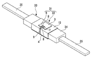
図2から図4は無線タグの第2実施形態を示しており、図4が完成した無線タグを示し、図2がその無線タグに使用されるフレキシブル回路板、図3が図2のフレキシブル回路板に集積回路チップを搭載する前の状態をそれぞれ示している。
この無線タグ11は、アンテナ12の基板をフレキシブル基板13により構成し、そのフレキシブル基板13を二つ折りにしてスペーサ14を間に介在させた構成としたものである。放射電極3、接地導体4、両導体線路7、9、及び集積回路チップ6の構成は第1実施形態のものと同じであり、同一符号を付して説明を簡略化する。
2 to 4 show a second embodiment of the wireless tag, FIG. 4 shows the completed wireless tag, FIG. 2 is a flexible circuit board used for the wireless tag, and FIG. 3 is the flexible circuit of FIG. A state before the integrated circuit chip is mounted on the plate is shown.
The
フレキシブル基板13は、PET(ポリエチレンテレフタレート)、ポリイミド等の誘電体の樹脂からなる25μm〜75μmのフィルム材によって構成されている。
このフレキシブル基板13の片面に、前記第1実施形態の放射電極、接地導体及び導体線路を平面状に展開したようなパターンで、放射電極3、接地導体4及び導体線路7、9が設けられている。この場合、フレキシブル基板13は幅寸法Wの2倍より少し大きい長さ寸法Lを有する長方形状に形成されており、その片面において、図2の一点鎖線Aで示す半分の位置よりも若干一方の端部寄りの位置の表面に、その一方の端部にわたって略正方形の接地導体4が設けられ、該接地導体4との間に間隔をおいて前記放射電極3が設けられている。この放射電極3は、フレキシブル基板13における前記接地導体4とは反対側の端部寄りに設けられており、フレキシブル基板13の両側辺からX=約λ/10ずつ内側に寄せて配置されている。
The
The
そして、これら放射電極3と接地導体4との間に、放射電極3の軸線C上に沿って両者から対向して延びる導体線路7、9が形成され、両導体線路7、9を接続するように集積回路チップ6が搭載されることにより、図2に示すフレキシブル回路板が構成される。放射電極3の給電点Q付近で導体線路7の両側にスリット8が設けられる点等、第1実施形態のものと同様である。
一方、スペーサ14は、シリコンゴム等の軟質の樹脂から構成されており、前記接地導体3とほぼ同じ大きさの略正方形の板状に形成され、厚さは約1.0mmに設定されている。
And between these
On the other hand, the
なお、集積回路チップ6を搭載する前の状態のフレキシブル回路板は、図3に示すように、放射電極3と接地導体4との間に、両者からそれぞれ他方に向けて延びる導体線路7・9が設けられるとともに、両導体線路7・9の先端が対向状態に配置され、これら対向状態の両導体線路7・9の間に、集積回路チップ6を搭載するためのチップ搭載部Eが形成されている。このチップ搭載部Eに各導体線路7・9に接続状態に集積回路チップ6を搭載することにより、図2に示す状態となるのである。
As shown in FIG. 3, the flexible circuit board in the state before mounting the
そして、図4に示すように、前記フレキシブル基板13は放射導体3等の形成面を表側(外側)にして二つ折りにされ、その間にスペーサ14が介在した状態とされ、両者が接着剤15によって固定されている。詳細には、フレキシブル基板13は、接地導体4が設けられている端部の裏面にスペーサ14の一方の面を接着剤15によって固定し、スペーサ14の一側面の両縁によってフレキシブル基板13を図2の二点鎖線Bで示す位置からそれぞれ折り曲げ、折り曲げられたフレキシブル基板13の端部をスペーサ14の他方の面に接着剤15によって固定することにより、製作される。この組み立てた後の構造においては、無線タグ11は、前記第1実施形態とほぼ同じ形状、寸法のものとなる。
As shown in FIG. 4, the
このように構成した無線タグ11は、フレキシブル基板13と軟質材からなるスペーサ14とによって基板が構成されているので、これを湾曲させることが可能であり、缶などの湾曲面を有する対象物品に取り付けることができる。
また、製造に際しては、フレキシブル基板13やスペーサ14をロール状のものから切り出しながら製作することができる。また、フレキシブル基板13は、銅を積層した基板からエッチング処理によって複数個同時に製作することも可能であり、生産性を著しく向上させることができる。
Since the
In manufacturing, the
この場合、フレキシブル基板13を折り曲げた際に、放射電極3は接地導体4の中央位置に重ねられるように配置されるが、接地導体4は放射電極3に比べて大きい面積に形成されているので、フレキシブル基板13を折り曲げた際にわずかにずれが生じたとしてもアンテナ12としての精度には影響が少なく、精密な位置決め作業が要求されないので、比較的容易に製作することができる。
なお、この第2実施形態の無線タグ11では、フレキシブル基板13の厚さが25μm〜75μmであり、これを単に二つ折りにしただけでは放射電極3と接地導体4との離間距離が確保できないので、二つ折りした間にスペーサ14を介在させるように構成したが、数百μmの厚さのフレキシブル基板を用いることができれば、スペーサは省略することが可能である。
In this case, when the
In the
以下、図5から図7は、図2及び図3に示すフレキシブル回路板を使用した他の実施形態の無線タグを示している。
図5は第3実施形態の無線タグを示している。この無線タグ21は、アンテナ22が第2実施形態の場合と同じように、フレキシブル基板13とスペーサ14とを有する構成とされているが、フレキシブル基板13は、放射電極3等の形成面を内側にして折り曲げられている点が異なるものである。このため、フレキシブル基板13の表面から突出する集積回路チップ6はスペーサ14に対向することになり、その対向位置のスペーサ14に、集積回路チップ6よりも大きい凹部23が形成されている。したがって、組み立て状態においては、集積回路チップ6がスペーサ14の凹部23内に収容され、フレキシブル基板13の外面に突出部分がなく、平坦面とされている。
Hereinafter, FIG. 5 to FIG. 7 show wireless tags of other embodiments using the flexible circuit board shown in FIG. 2 and FIG.
FIG. 5 shows a wireless tag according to the third embodiment. As in the case of the second embodiment, the
このように集積回路チップ6をフレキシブル基板13の内側に配置して外側に露出しないようにしたことにより、集積回路チップ6が外力から有効に保護される。
すなわち、集積回路チップ6を実装する場合、ベアチップをフリップチップ実装するか、ICパッケージ化してハンダ付けする等の方法があるが、単に基板上にフリップチップ実装するだけではチップが露出状態となるし、ICパッケージ化の方法ではパッケージ化のための工程が必要でコスト高を招く。本実施形態の場合、図5に示すように、フリップチップ実装した集積回路チップ6を二つ折りにしたフレキシブル基板13の内側に配置するという簡単な構成により、集積回路チップ6の保護を確実にすることができるのである。
As described above, the
That is, when the
図6は第4実施形態の無線タグを示しており、この無線タグ31は、アンテナ32のフレキシブル基板13及びその片面に形成される放射電極3、接地導体4、導体回路7、9並びに集積回路チップ6の構成は第2実施形態及び第3実施形態のものと同じであるが、折り曲げたフレキシブル基板13の間に介在されるスペーサ33がリストバンドの形態をしている点が両実施形態のものと異なる点である。
すなわち、このスペーサ33は、フレキシブル基板13が貼り付けられる基台部34と、該基台部34の両端から一体に延びる一対のバンド部35とから構成されており、バンド部35の先端部には、相互に着脱可能なマジックテープ(登録商標)等の留め具(図示略)が設けられる。基台部34とバンド部35とは、同一の厚みにより1枚のシートから型抜き等で成形されてもよい。
FIG. 6 shows a wireless tag according to the fourth embodiment. The
That is, the spacer 33 includes a
そして、その基台部34は直方体状に形成され、該基台部34を挟むように図2に示すものと同様のフレキシブル基板13が二つ折り状態で貼り付けられていることにより、その上面に放射電極3、下面に接地導体4が配置されるとともに、側面に接地導体4からの導体線路9が引き出され、上面で集積回路チップ6に接続されている。
And the
このように構成した無線タグ31は、スペーサ33であるリストバンドを腕等に巻き付けて使用され、遊園地等において入園者の入退場管理に適用することができる。
この種の無線タグは、従来では、例えば成形樹脂中に埋め込まれており、成形金型内で無線タグをインサート成形することにより製作されるので、コスト高となっていたが、この実施形態の構成とすることにより、フレキシブル基板13とスペーサ33とを別々にかつ連続的に製作しておくことができ、生産性が著しく向上するものである。
なお、この第4実施形態の無線タグ31においても、図5の第3実施形態のものと同様に、フレキシブル基板13をその回路形成面を内側にして折り曲げ、スペーサ33の基台部34に集積回路チップ6を収容する凹部を形成した構成とすれば、突出部のない平坦な外面に形成することができるとともに、集積回路チップ6を外力から保護することができる。
The
Conventionally, this type of wireless tag is embedded in, for example, a molding resin, and is manufactured by insert molding the wireless tag in a molding die. By adopting the configuration, the
In the
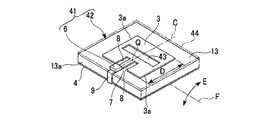
図7は第5実施形態の無線タグを示しており、この無線タグ41は、基本的な構成は第2実施形態の無線タグと同様であるが、アンテナ42の放射電極3及び接地導体4に切欠部43を形成したものである。つまり、放射電極3及び接地導体4のほぼ中央位置(図7では接地導体6の切欠部は隠れて見えない)に、放射電極3の軸線Cに直交する方向に沿うスロット状の切欠部43が形成されている。図中符号44は放射電極3及び集積回路チップ6を覆う保護層を示しており、薄肉の樹脂フィルムによって構成される。
FIG. 7 shows the wireless tag of the fifth embodiment. The wireless tag 41 has the same basic configuration as that of the wireless tag of the second embodiment, but is connected to the
この無線タグ41においては、フレキシブル基板13及びスペーサ14が可とう性を有しているので、全体に曲げ変形させて使用することができるが、その場合に、この無線タグ41では、フレキシブル基板13が折り曲げて形成されているので、その折り曲げ部13aをさらに直交方向に曲げ変形させることには限界がある。そこで、図7の矢印Eで示すように軸線Cを湾曲させる方向に曲げ変形させることになり、そのときに曲げ変形の内側に配置される面(図7では接地導体4の表面)には圧縮力が作用して接地導体4を構成している銅箔にしわが生じ易いが、その部分に、放射電極3の軸線Cに直交する方向の線Fに沿ってスロット状の切欠部43が形成されているので、しわの発生が防止されるのである。したがって、曲げ変形が予定される場合に、その曲げ変形予定位置に、曲げ変形予定線(図7の場合は線F)に沿って切欠部43を形成すればよい。
この無線タグ41において、アンテナ42は、放射電極3において通信に寄与する一対の辺(開放端)3aが所定の長さD=約λ/4に設定されていれば通信可能であり、その開放端3aが維持される範囲で切欠部43が形成されていても通信には影響を与えない。
In this wireless tag 41, since the
In this wireless tag 41, the antenna 42 can communicate if the pair of sides (open ends) 3 a that contribute to communication in the
なお、本発明は、前記の各実施形態に限定されるものではなく、本発明の趣旨を逸脱しない範囲において種々の変更を加えることが可能である。例えば、図7の第5実施形態で示した保護層を図1の第1実施形態等、集積回路チップ6が表面に露出する形態のものに適用することができる。また、基板やスペーサの形状等も取り付けられる対象の物品形状等に合わせて適宜変更可能である。例えば、本やCDケース、各種カード等の端部をスペーサとして無線タグを構成することができる。
The present invention is not limited to the above-described embodiments, and various modifications can be made without departing from the spirit of the present invention. For example, the protective layer shown in the fifth embodiment of FIG. 7 can be applied to a structure in which the
1…無線タグ 2…基板 3…放射電極 4…接地導体 5…アンテナ 6…集積回路チップ 7…導体線路 8…スリット 9…導体線路 11…無線タグ 12…アンテナ 13…フレキシブル基板 14…スペーサ 15…接着剤 21…無線タグ 22…アンテナ 31…無線タグ 32…アンテナ 33…スペーサ 34…基台部 35…バンド部 41…無線タグ 42…アンテナ 43…切欠部 44…保護層 E…集積回路チップ搭載部
DESCRIPTION OF SYMBOLS 1 ... Wireless tag 2 ... Board |
Claims (4)
前記基板はフレキシブル基板を二つ折り状に折り曲げて構成され、
二つ折り状の前記フレキシブル基板の間にスペーサが挿入状態に固定され、
前記スペーサは可とう性を有する軟質材から構成され、
前記放射電極及び/又は接地導体には、その曲げ変形予定線に沿う切欠部が形成されていることを特徴とする無線タグ。 A radiation electrode is provided on one main surface of the substrate made of a dielectric, and a ground conductor is provided on the other main surface, and an integrated circuit chip on which information is recorded between the radiation electrode and the ground conductor; A conductor line that connects the integrated circuit chip to the radiation electrode and the ground conductor, respectively, and the conductor line is formed on the side surface of the substrate ;
The substrate is formed by folding a flexible substrate in a fold shape,
A spacer is fixed in an inserted state between the two folded flexible substrates,
The spacer is composed of a flexible soft material,
The radio tag according to claim 1, wherein the radiation electrode and / or the ground conductor is formed with a notch along a planned bending deformation line .
Priority Applications (1)
| Application Number | Priority Date | Filing Date | Title |
|---|---|---|---|
| JP2006211894A JP4169062B2 (en) | 2006-08-03 | 2006-08-03 | Wireless tag |
Applications Claiming Priority (1)
| Application Number | Priority Date | Filing Date | Title |
|---|---|---|---|
| JP2006211894A JP4169062B2 (en) | 2006-08-03 | 2006-08-03 | Wireless tag |
Publications (2)
| Publication Number | Publication Date |
|---|---|
| JP2008042379A JP2008042379A (en) | 2008-02-21 |
| JP4169062B2 true JP4169062B2 (en) | 2008-10-22 |
Family
ID=39176938
Family Applications (1)
| Application Number | Title | Priority Date | Filing Date |
|---|---|---|---|
| JP2006211894A Active JP4169062B2 (en) | 2006-08-03 | 2006-08-03 | Wireless tag |
Country Status (1)
| Country | Link |
|---|---|
| JP (1) | JP4169062B2 (en) |
Families Citing this family (36)
| Publication number | Priority date | Publication date | Assignee | Title |
|---|---|---|---|---|
| WO2009013817A1 (en) | 2007-07-25 | 2009-01-29 | Fujitsu Limited | Wireless tag |
| JP4770853B2 (en) * | 2008-02-27 | 2011-09-14 | 三菱電機株式会社 | RFID tag and manufacturing method thereof |
| JP2009260758A (en) * | 2008-04-18 | 2009-11-05 | Murata Mfg Co Ltd | Radio ic device |
| EP2284949B1 (en) | 2008-05-21 | 2016-08-03 | Murata Manufacturing Co. Ltd. | Wireless ic device |
| CN102047271B (en) | 2008-05-26 | 2014-12-17 | 株式会社村田制作所 | Wireless IC device system and method for authenticating wireless IC device |
| JP5103526B2 (en) * | 2008-07-11 | 2012-12-19 | 日立Geニュークリア・エナジー株式会社 | IC tag device |
| DE112009002384B4 (en) | 2008-11-17 | 2021-05-06 | Murata Manufacturing Co., Ltd. | Antenna and wireless IC component |
| JP5510450B2 (en) | 2009-04-14 | 2014-06-04 | 株式会社村田製作所 | Wireless IC device |
| EP2568534A3 (en) | 2009-04-21 | 2014-05-14 | Murata Manufacturing Co., Ltd. | Antenna devie and method of setting resonant frequency of antenna device |
| JP5304580B2 (en) | 2009-10-02 | 2013-10-02 | 株式会社村田製作所 | Wireless IC device |
| JP5327334B2 (en) | 2009-11-04 | 2013-10-30 | 株式会社村田製作所 | Communication terminal and information processing system |
| CN102792520B (en) | 2010-03-03 | 2017-08-25 | 株式会社村田制作所 | Wireless communication module and Wireless Telecom Equipment |
| WO2011118379A1 (en) | 2010-03-24 | 2011-09-29 | 株式会社村田製作所 | Rfid system |
| JP5630499B2 (en) | 2010-03-31 | 2014-11-26 | 株式会社村田製作所 | Antenna apparatus and wireless communication device |
| JP5170156B2 (en) * | 2010-05-14 | 2013-03-27 | 株式会社村田製作所 | Wireless IC device |
| JP5299351B2 (en) * | 2010-05-14 | 2013-09-25 | 株式会社村田製作所 | Wireless IC device |
| WO2012014939A1 (en) | 2010-07-28 | 2012-02-02 | 株式会社村田製作所 | Antenna device and communications terminal device |
| JP2012146000A (en) * | 2011-01-07 | 2012-08-02 | Murata Mfg Co Ltd | Radio ic device |
| CN104899639B (en) | 2011-02-28 | 2018-08-07 | 株式会社村田制作所 | Wireless communication devices |
| WO2012157596A1 (en) * | 2011-05-16 | 2012-11-22 | 株式会社村田製作所 | Wireless ic device |
| JP5703977B2 (en) * | 2011-06-07 | 2015-04-22 | 株式会社村田製作所 | Metal articles with wireless communication devices |
| JP5828249B2 (en) * | 2011-09-02 | 2015-12-02 | 凸版印刷株式会社 | Non-contact IC label |
| CN203553354U (en) | 2011-09-09 | 2014-04-16 | 株式会社村田制作所 | Antenna device and wireless device |
| JP5915115B2 (en) * | 2011-11-24 | 2016-05-11 | 凸版印刷株式会社 | Antenna unit |
| JP5344108B1 (en) | 2011-12-01 | 2013-11-20 | 株式会社村田製作所 | Wireless IC device and manufacturing method thereof |
| WO2013125610A1 (en) | 2012-02-24 | 2013-08-29 | 株式会社村田製作所 | Antenna device and wireless communication device |
| JPWO2013145312A1 (en) * | 2012-03-30 | 2015-08-03 | 富士通株式会社 | RFID tag |
| WO2013145312A1 (en) * | 2012-03-30 | 2013-10-03 | 富士通株式会社 | Rfid tag |
| WO2013153697A1 (en) | 2012-04-13 | 2013-10-17 | 株式会社村田製作所 | Rfid tag inspection method, and inspection device |
| JP2014127752A (en) * | 2012-12-25 | 2014-07-07 | Smart:Kk | Antenna and system using the same |
| JP6040784B2 (en) * | 2013-01-23 | 2016-12-07 | 凸版印刷株式会社 | Non-contact IC label and article with non-contact IC label |
| CN105074787A (en) * | 2013-02-25 | 2015-11-18 | 林利有限公司 | Mobile communication devices |
| JP5687754B2 (en) * | 2013-12-05 | 2015-03-18 | アピックヤマダ株式会社 | RFID tag |
| TWI607601B (en) | 2015-02-10 | 2017-12-01 | Phoenix Solution Co Ltd | RF tag antenna and its manufacturing method and RF tag |
| KR102327550B1 (en) * | 2018-03-06 | 2021-11-16 | 동우 화인켐 주식회사 | Film antenna and display device including the same |
| CN114335987B (en) * | 2022-03-15 | 2022-06-07 | 英内物联网科技启东有限公司 | Antenna module with RFID electronic tag formula |
-
2006
- 2006-08-03 JP JP2006211894A patent/JP4169062B2/en active Active
Also Published As
| Publication number | Publication date |
|---|---|
| JP2008042379A (en) | 2008-02-21 |
Similar Documents
| Publication | Publication Date | Title |
|---|---|---|
| JP4169062B2 (en) | Wireless tag | |
| KR100679502B1 (en) | Rfid tag, rfid-tag antenna, rfid-tag antenna sheet, and method of manufacturing rfid tag | |
| JP5703977B2 (en) | Metal articles with wireless communication devices | |
| US7924228B2 (en) | Storage medium with built-in antenna | |
| JP6512385B2 (en) | RFID tag | |
| US8937576B2 (en) | Wireless communication device | |
| JPWO2007000807A1 (en) | Radio frequency identification tag | |
| JP4894923B2 (en) | Loop antenna | |
| EP1713025B1 (en) | RFID tag set and RFID tag | |
| WO2007013167A1 (en) | Rf tag and rf tag manufacturing method | |
| CN209963236U (en) | Wireless communication device | |
| JP2012253699A (en) | Wireless communication device, its manufacturing method, and metal article with wireless communication device | |
| JP6785966B2 (en) | RFID-tagged package | |
| US9922283B2 (en) | RFID tag and high frequency circuit | |
| JP2006309324A (en) | Radio tag | |
| JP2019004266A (en) | Antenna device and electronic apparatus | |
| JP6911958B2 (en) | Packaging paperboard and its manufacturing method | |
| JP2008217613A (en) | Contactless type data carrier device | |
| JP5098588B2 (en) | Non-contact type IC tag and method of manufacturing non-contact type IC tag | |
| JP7176313B2 (en) | RF tag label | |
| JP2012252664A (en) | Radio communication device, manufacturing method thereof, and metal article with radio communication device | |
| JP4894246B2 (en) | IC tag base sheet | |
| JP7356659B2 (en) | IC tags and composite IC cards | |
| JP2020046834A (en) | RF tag label | |
| US20230359847A1 (en) | Container including rfid module |
Legal Events
| Date | Code | Title | Description |
|---|---|---|---|
| A131 | Notification of reasons for refusal |
Free format text: JAPANESE INTERMEDIATE CODE: A131 Effective date: 20080422 |
|
| A521 | Request for written amendment filed |
Free format text: JAPANESE INTERMEDIATE CODE: A523 Effective date: 20080623 |
|
| TRDD | Decision of grant or rejection written | ||
| A01 | Written decision to grant a patent or to grant a registration (utility model) |
Free format text: JAPANESE INTERMEDIATE CODE: A01 Effective date: 20080715 |
|
| A01 | Written decision to grant a patent or to grant a registration (utility model) |
Free format text: JAPANESE INTERMEDIATE CODE: A01 |
|
| A61 | First payment of annual fees (during grant procedure) |
Free format text: JAPANESE INTERMEDIATE CODE: A61 Effective date: 20080728 |
|
| FPAY | Renewal fee payment (event date is renewal date of database) |
Free format text: PAYMENT UNTIL: 20110815 Year of fee payment: 3 |
|
| R150 | Certificate of patent or registration of utility model |
Ref document number: 4169062 Country of ref document: JP Free format text: JAPANESE INTERMEDIATE CODE: R150 Free format text: JAPANESE INTERMEDIATE CODE: R150 |
|
| FPAY | Renewal fee payment (event date is renewal date of database) |
Free format text: PAYMENT UNTIL: 20110815 Year of fee payment: 3 |
|
| FPAY | Renewal fee payment (event date is renewal date of database) |
Free format text: PAYMENT UNTIL: 20120815 Year of fee payment: 4 |
|
| FPAY | Renewal fee payment (event date is renewal date of database) |
Free format text: PAYMENT UNTIL: 20120815 Year of fee payment: 4 |
|
| FPAY | Renewal fee payment (event date is renewal date of database) |
Free format text: PAYMENT UNTIL: 20130815 Year of fee payment: 5 |
|
| R250 | Receipt of annual fees |
Free format text: JAPANESE INTERMEDIATE CODE: R250 |
|
| R250 | Receipt of annual fees |
Free format text: JAPANESE INTERMEDIATE CODE: R250 |
|
| R250 | Receipt of annual fees |
Free format text: JAPANESE INTERMEDIATE CODE: R250 |
|
| R250 | Receipt of annual fees |
Free format text: JAPANESE INTERMEDIATE CODE: R250 |