JP4165165B2 - Liquid crystal display panel and electronic equipment - Google Patents
Liquid crystal display panel and electronic equipment Download PDFInfo
- Publication number
- JP4165165B2 JP4165165B2 JP2002280872A JP2002280872A JP4165165B2 JP 4165165 B2 JP4165165 B2 JP 4165165B2 JP 2002280872 A JP2002280872 A JP 2002280872A JP 2002280872 A JP2002280872 A JP 2002280872A JP 4165165 B2 JP4165165 B2 JP 4165165B2
- Authority
- JP
- Japan
- Prior art keywords
- liquid crystal
- region
- pixel
- display panel
- substrate
- Prior art date
- Legal status (The legal status is an assumption and is not a legal conclusion. Google has not performed a legal analysis and makes no representation as to the accuracy of the status listed.)
- Expired - Fee Related
Links
Images


Description
【0001】
【発明の属する技術分野】
本発明は、反射型表示および透過型表示が可能な液晶表示パネル、およびこの液晶表示パネルを備えた電子機器に関する。
【0002】
【従来の技術】
反射型表示と透過型表示とが可能ないわゆる半透過反射型の液晶表示パネルは、携帯電話機など各種の電子機器の表示デバイスとして広く用いられている。この種の液晶表示パネルは、液晶を挟持する一対の基板のうち背面側の基板の面上に、開口部を有する反射層が設けられた構成を採るのが一般的である。この構成のもと、観察側から入射した太陽光や室内照明光などの外光は上記反射層の表面で反射した後に観察側から出射し、これにより反射型表示が実現される。一方、背面側から入射したバックライトユニットなどの照射光は反射層に設けられた開口部を通過して観察側に出射し、これにより透過型表示が実現される。半透過反射型の液晶表示パネルによれば、外光が十分に存在する環境においてはバックライトユニットを消灯させて反射型表示を行なう一方、外光が不十分な環境においてはバックライトユニットを点灯させて透過型表示を行なうことにより表示画像の視認性を確保できるという利点がある(例えば特許文献1参照)。
【0003】
【特許文献1】
特開2002−14334号公報(第13頁、第14頁、第13図)
【0004】
【発明が解決しようとする課題】
ところで液晶表示パネルにおいては、相互に隣接する画素間の電圧差に起因して横方向電界が発生し、この横方向電界の影響によって液晶分子が所期の配向方向とは異なる方向に配向するという現象(以下「ディスクリネーション」という)が生じ得る。このように液晶分子の配向方向が乱れると光が所期の偏光方向に変調されないため、各画素のうちディスクリネーションが発生した領域では色再現性の低下や表示欠陥といった表示品位に重大な影響を与え得る不具合が生じる。
【0005】
そして、上述した半透過反射型の液晶表示パネルにおいては、画素のうち反射型表示のために光を反射させる領域(以下「反射領域」という)と、この画素のうち透過型表示のために光を透過させる領域(以下「透過領域」という)との面積比率が、ディスクリネーションに起因して所期の比率とは異なってしまうという問題があった。すなわち、例えば透過領域のみにおいてディスクリネーションが発生した場合には、当該透過領域のうち画像表示に有効に寄与する面積が実質的に縮小されることとなるため、透過領域の面積が反射領域の面積と比較して相対的に狭くなる。そしてこのように反射領域と透過領域との面積比率に偏りが生じると、表示方式によって表示品位のばらつきが生じるという問題を招くおそれがある。特に、近年における表示画像の高精細化の要求に応えるべく画素の面積を小さくした場合には、各画素のうちディスクリネーションが発生する領域の占める割合が相対的に増大するため、上述した問題はいっそう顕著なものとなる。
【0006】
本発明は以上説明した事情に鑑みてなされたものであり、ディスクリネーションに起因して反射領域と透過領域との面積比率に偏りが生じるのを抑えることができる液晶表示パネル、およびこの液晶表示パネルを備えた電子機器を提供することを目的としている。
【0007】
【課題を解決するための手段】
上記課題を解決するために、本発明の特徴は、第1基板に設けられた電極と、液晶を挟んで前記第1基板に対向する第2基板に設けられた電極との交差領域を画素とし、前記画素がXおよびY方向にわたってマトリクス状に配列する液晶表示パネルにおいて、前記第2基板に設けられて前記第1基板側からの入射光を反射させる反射層であって、前記画素のうち当該反射層によって前記第1基板側からの入射光を反射させる反射領域と、当該画素のうち前記第2基板側からの入射光を前記第1基板側に透過させる透過領域とを有し、前記画素は、略矩形状であり、前記反射領域は、前記画素の周縁のうち、前記Y方向の両縁端部に設けられ、前記透過領域は、前記画素における反射領域で挟まれた領域であり、前記反射層によって前記第1基板側からの入射光を反射させる反射領域のうちディスクリネーション発生領域に相当する部分の面積と、前記第2基板側からの入射光を前記第1基板側に透過させる透過領域のうち当該ディスクリネーション発生領域に相当する部分の面積とが略等しいことにある。
【0008】
この構成によれば、画素における一部の周縁を横切るように反射層が設けられているから、当該画素のうち反射層によって第1基板側からの入射光を反射させる反射領域と、当該画素のうち第2基板側からの入射光を第1基板側に透過させる透過領域とが、画素の周縁に沿って隣接する。したがって、画素の周縁に沿ってディスクリネーションが発生したときに、当該ディスクリネーションの発生する領域が反射領域と透過領域の双方にわたることとなる。この結果、反射領域および透過領域のいずれか一方のみにおいてディスクリネーションが発生するのを避けることができるから、ディスクリネーションに起因して反射領域と透過領域との面積比率に偏りが生じるのを抑えることができる。
【0011】
上記特徴を有する本発明に係る液晶表示パネルにおいては、ディスクリネーションに起因して表示欠陥となる面積を反射領域と透過領域とにおいて等しいから、反射型表示のときの表示品位と透過型表示のときの表示品位との差異をより確実に抑えることができる。
【0013】
一方、それぞれ異なる色が割り当てられた複数の画素を有する液晶表示パネル、すなわち反射層よりも観察側において前記各画素と重なるように設けられて当該画素の色に対応する波長の光を選択的に透過させる複数のカラーフィルタを具備する液晶表示パネルに本発明を適用する場合には、それぞれ異なる色に対応する前記複数の画素のうち少なくとも一の画素と他の画素とにおいて、前記反射層によって前記第1基板側からの入射光を反射させる反射領域と前記第2基板側からの入射光を前記第1基板側に透過させる透過領域との面積比率を異ならせてもよい。この構成によれば、反射型表示のときに反射層の表面で反射されて観察側に出射する光量を各色の画素ごとに任意に設定することができる。したがって、例えば各色の画素における反射領域と透過領域との面積比率を各カラーフィルタの透過率に応じて選定すれば、各色ごとの透過率のばらつきを補償して良好な色再現性を実現することができる。また、例えばバックライトユニットによる照射光に分光特性のばらつきがある場合(すなわち各波長の光量が相違する場合)であっても、各画素における反射領域と透過領域との面積比率をこの分光特性に応じて選定すれば、分光特性のばらつきを補償して良好な色再現性が実現される。
【0014】
また、複数のカラーフィルタのうち少なくとも一の色のカラーフィルタとして、当該カラーフィルタに対応する前記画素のうち前記反射層と重なる領域内に開口部を有するものを用いてもよい。この構成によれば、反射型表示のときにカラーフィルタを透過して観察側に出射する光量を開口部の面積に応じて任意に設定することができる。さらに、カラーフィルタに開口部を設けた液晶表示パネルにおいては、少なくとも一の色のカラーフィルタの開口部の面積と、他の色のカラーフィルタの開口部の面積とを異ならせてもよい。こうすれば、各色のカラーフィルタの透過率の相違を補償して良好な色再現性を実現することができる。
【0015】
また、本発明に係る電子機器は、本発明に係る液晶表示パネルを表示装置として備えたことを特徴としている。上述したように、本発明に係る液晶表示パネルによれば、ディスクリネーションに起因して反射領域と透過領域との面積比率に偏りが生じるのを抑えることができるから、使用環境に応じて反射型表示と透過型表示とが切り替えられ、しかも双方の表示方式において高い表示品位が要求される電子機器に搭載される表示装置として特に好適である。このような電子機器としては、例えば可搬型のパーソナルコンピュータや携帯電話機などが考えられる。
【0016】
【発明の実施の形態】
以下、図面を参照して本発明の実施の形態を説明する。なお、以下に示す各図においては、図面が煩雑になるのを防ぐために各構成要素の寸法や比率などを実際のものとは適宜に異ならせてある。
【0017】
<A:実施形態の構成>
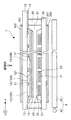
まず、図1を参照して、本発明をパッシブマトリクス方式の半透過反射型液晶表示パネルに適用した形態について説明する。同図に示すように、本実施形態に係る液晶表示装置は液晶表示パネル1とバックライトユニット4とを有する。このうち液晶表示パネル1は、第1基板10と第2基板20とがシール材30を介して貼り合わされるとともに、両基板とシール材30とによって囲まれた領域に、例えばTN(Twisted Nematic)型やSTN(Super Twisted Nematic)型などの液晶31が封入された構成となっている。バックライトユニット4は、液晶表示パネル1の第2基板20側に配置されている。以下では、図1に示すように、液晶表示パネル1に対してバックライトユニット4とは反対側を「観察側」と表記する。すなわち「観察側」とは、当該液晶表示パネル1による表示画像を視認する観察者が位置する側という意味である。
【0018】
バックライトユニット4は、光源41と導光板42とを有する。このうち光源41は、例えばLED(Light Emitting Diode)や冷陰極管などにより構成され、導光板42の側端面に対して光を照射する。一方、導光板42は、その側端面に入射した光源41からの光を液晶表示パネル1の基板面に対して一様に導くための板状部材である。導光板42のうち液晶表示パネル1と対向する面には、当該導光板42からの出射光を液晶表示パネル1に対して一様に拡散させる拡散板などが貼着される一方、これと反対側の面には、導光板42から液晶表示パネル1とは反対側に出射した光を液晶表示パネル1側に反射させる反射板が貼着される(いずれも図示略)。なお、光源41は常に点灯しているわけではなく、外光が十分に存在しない環境において使用される場合に、ユーザからの指示やセンサからの検出信号に応じて点灯する。
【0019】
一方、液晶表示パネル1の第1基板10および第2基板20は、ガラスやプラスチックなどの光透過性を有する板状部材である。このうち第1基板10の外側(液晶31とは反対側)表面には、干渉色を補償するための位相差板101と、入射光を偏光させるための偏光板102とが貼着されている。一方、第2基板20の外側(液晶31とは反対側)表面にも同様に位相差板201と偏光板202とが貼着されている。
【0020】
第1基板10の面上には複数のコモン電極14が設けられている。ここで、図2は、液晶表示パネル1を構成する一部の構成要素を拡大して示す平面図である。図2におけるA−A’線からみた断面図が図1に相当する。図1および図2に示すように、複数のコモン電極14は相互に離間してx軸方向に延在する帯状の電極である。各コモン電極14は、例えばITO(Indium Tin Oxide)などの透明導電材料によって形成される。
【0021】
一方、第2基板20の面上には複数のセグメント電極22が設けられている。各セグメント電極22は、コモン電極14と同様にITOなどの透明導電材料によって形成された帯状の電極であり、図1および図2に示すようにコモン電極14と交差する方向(すなわち図中のy軸方向)に延在する。図1に示すように、コモン電極14が形成された第1基板10の表面、およびセグメント電極22が形成された第2基板20の表面は、それぞれ配向膜15および23によって覆われている。配向膜15および23は、例えばポリイミドなどによって形成された有機薄膜であり、電圧が印加されていないときの液晶31の配向方向を規定するためのラビング処理が施されている。
【0022】
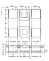
第1基板10と第2基板20との間に挟持された液晶31は、コモン電極14とセグメント電極22との間に印加された電圧に応じてその配向方向が変化する。以下では、図2の右下部分に示すように、コモン電極14とセグメント電極22とが対向する領域5を「画素」と表記する。すなわち、画素5は、電圧の印加に応じて液晶31の配向方向が変化させられる領域の最小単位であるということができる。図2に示すように、複数の画素5はx軸方向およびy軸方向にわたってマトリクス状に配列し、各々が赤色(R)、緑色(G)および青色(B)のうちのいずれかに対応している。そして、これらの3色に対応する3つの画素5R、5Gおよび5Bによって、表示画像の最小単位に相当するドットが構成される。
【0023】
また、図1に示すように第1基板10の内側(液晶31側)表面には、遮光層11、カラーフィルタ12およびオーバーコート層13が形成されている。このうちオーバーコート層13は、例えばアクリル系やエポキシ系などの樹脂材料やSiO2などの無機材料によって形成され、遮光層11とカラーフィルタ12との段差を平坦化する役割を担っている。上述したコモン電極14および配向膜15は、オーバーコート層13の表面に形成されている。一方、遮光層11は、マトリクス状に配列する各画素5の間隙(すなわちコモン電極14とセグメント電極22とが対向する領域以外の領域)を覆うように格子状に形成されて各画素5の周囲を遮光する。この遮光層11は、例えばカーボンブラックが分散された樹脂材料や、クロム(Cr)などの金属によって形成される。
【0024】
次に、カラーフィルタ12(12R、12Gおよび12B)は、各画素5に対応して形成された樹脂層であり、染料や顔料によって赤色、緑色および青色のいずれかにそれぞれ着色されている。したがって、液晶31を透過して第1基板10に向かう光のうち各カラーフィルタ12の色に対応した波長の光が選択的に観察側に出射することとなる。また、緑色のカラーフィルタ12Gの中央部近傍には、図1に示すように開口部121が設けられているが、この点については後に詳述する。なお、本実施形態においては、y軸方向に列をなす複数の画素5にわたって同一色のカラーフィルタ12が配列された構成(いわゆるストライプ配列)が採用された場合を例示するが、この種の配列パターンを採用した液晶表示パネル1に本発明の適用範囲を限定する趣旨ではない。
【0025】
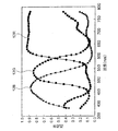
ここで、図3は、本実施形態において用いられるカラーフィルタ12の透過率特性を表す図である。なお、同図においてはカラーフィルタ12への入射光の波長が横軸に、透過率(入射光量に対する出射光量の割合)が縦軸にそれぞれ示されている。同図に示すように、カラーフィルタ12Rは赤色に対応する約600nm(ナノメートル)以上の波長に対して高い透過率を示し、カラーフィルタ12Gは緑色に対応する約500nm〜600nmの波長の光に対して高い透過率を示し、カラーフィルタ12Bは青色に対応する約400nm〜500nmの波長の光に対して高い透過率を示すようになっている。そして、図3において各カラーフィルタ12の最大透過率を比較すると、緑色のカラーフィルタ12Gの最大透過率(約0.84)が、赤色のカラーフィルタ12Rの最大透過率(0.92)および青色のカラーフィルタ12の最大透過率(0.89)よりも小さくなっていることが判る。すなわち、同一の光量を各色のカラーフィルタ12に照射したと仮定したとき、緑色のカラーフィルタ12Gからの出射光量は、赤色のカラーフィルタ12Rおよび青色のカラーフィルタ12Bからの出射光量よりも少ない。
【0026】
一方、図1および図2に示すように、第2基板20の内側(液晶31側)には複数の反射層21が設けられている。各反射層21は、第1基板10側からの入射光を反射させるための層であり、例えばアルミニウムや銀などの単体金属、またはこれらを主成分として含む合金などによって形成されて光反射性を有する。本実施形態における反射層21は、銀(Ag)を主成分としてパラジウム(Pd)および銅(Cu)を含む合金によって形成されているものとする。また、第2基板20の内側表面は、反射層21の表面に散乱構造(凹凸)を形成するために粗面化されているが図示は省略されている。なお、反射層21の表面に散乱構造を形成する構成に代えて、観察側の偏光板102に散乱特性を持たせた、いわゆる前方散乱方式を採用してもよい。
【0027】
ここで、図4は、反射層21とセグメント電極22との位置関係を示す図であって、図2におけるB−B’線からみた断面(すなわちセグメント電極22の横断面)を示す図である。同図に示すように反射層21は、その断面の全周縁にわたってセグメント電極22に覆われている。より具体的には、図4に示すように、セグメント電極22の一部を構成する第1層221が第2基板20の表面に形成されるとともに、この第1層221のうち幅方向の一部分を覆うように反射層21が形成されている。さらに、第1層221とともにセグメント電極22を構成する第2層222が、反射層21のうち第2基板20と平行な面から幅方向の周縁部(エッジ部分)にわたって当該反射層21を覆うように形成される。この構成により、セグメント電極22と反射層21とは電気的に接続される。セグメント電極22を構成するITOは抵抗値が比較的高いのに対し、反射層21を構成する合金は抵抗値が低い。このため、図4に示したようにセグメント電極22と反射層21とを導通させることによって配線抵抗が低く抑えられる。
【0028】
一方、図2に示すように第2基板20の板面と平行な面に着目すると、複数の反射層21の各々は画素5の一部と重なるようになっている。そして、画素5のうち反射層21と重なる領域(以下「反射領域」という)51は、第1基板10側からの入射光を反射して反射型表示を行なうための領域として機能する。すなわち、反射型表示を行なうとき、観察側から液晶表示パネル1に入射した太陽光や室内照明光などの外光は、偏光板102および位相差板101を通過することによって所定の偏光状態となった後、第1基板10→カラーフィルタ12→コモン電極14→液晶31→セグメント電極22という経路を辿って反射層21に至るとともに、その表面において反射して上記経路を逆に辿る。このとき、コモン電極14とセグメント電極22との間の電圧差に応じて液晶31の配向状態が変化するため、反射領域51における反射光のうち偏光板102を通過して観察者に視認される光量が画素5ごとに制御されるのである。
【0029】
一方、画素5のうち反射層21によって覆われた領域以外の領域(以下「透過領域」という)52は、第2基板20に入射したバックライトユニット4からの照射光を観察側に透過させて透過型表示を行なうための領域として機能する。すなわち、透過型表示を行なうとき、バックライトユニット4による照射光は、偏光板202および位相差板201を透過することによって所定の偏光状態となった後、第2基板20→(透過領域52→)セグメント電極22→液晶31→コモン電極14→カラーフィルタ12→第1基板10という経路を辿って観察側に出射する。この透過型表示においても、コモン電極14とセグメント電極22との間の電圧差に応じて液晶31の配向状態が変化するため、透過領域52を透過した光のうち偏光板102を透過して観察者に視認される光量は画素5ごとに制御される。
【0030】
次に、カラーフィルタ12のより詳細な構成について説明する。図5は、ひとつのドットを構成する3色分の画素5(5R、5Bおよび5G)を拡大して示す図である。同図に示すように、3色のカラーフィルタ12のうち緑色のカラーフィルタ12Gには、画素5のうち反射領域51の内側と重なるように開口部121が設けられている。この開口部121は、カラーフィルタ12が存在しない部分であり、この開口部121にはカラーフィルタ12および遮光層11を覆うオーバーコート層13が入り込んでいる。図3を例にとって上述したように、緑色のカラーフィルタ12Gの透過率は、他色のカラーフィルタ12の透過率と比較して低い。このため、仮に緑色のカラーフィルタ12Gに開口部121を設けないとすれば、反射型表示が行なわれるときに、緑色のカラーフィルタ12Gを透過する光量が、赤色のカラーフィルタ12Rおよび青色のカラーフィルタ12Bを透過する光量よりも少なくなる。したがって、反射型表示のときに赤色、緑色および青色の各色について観察者に認識される光量がばらつき、ひいては良好な色再現性を確保することが困難となるおそれがある。これに対し本実施形態においては、透過率の低い緑色のカラーフィルタ12Gに開口部121が設けられているため、反射型表示のときに赤色、緑色および青色の各色について観察者に視認される光量のバランスを保つことができるのである。
【0031】
一方、図2に示すように、本実施形態における反射層21は、画素5のうちコモン電極14における幅方向の両縁辺近傍と重なるように設けられている。したがって、ひとつの画素5に着目すると、透過領域52が、セグメント電極22の延在方向(y軸方向)において反射領域51によって挟まれることとなる。そして、図2および図5に示すように、反射領域51および透過領域52の面積比率は、各色の画素5ごとに、各カラーフィルタ12の透過率特性に応じて異なっている。具体的には、緑色の画素5Gにおける反射領域51の面積は、赤色の画素5Rおよび青色の画素5Bにおける反射領域51の面積よりも大きくなっている。ここで、緑色のカラーフィルタ12Gの透過率は他色のカラーフィルタ12の透過率よりも低いため、仮にすべての色の画素5について反射領域51の面積を等しくするとすれば(つまり反射領域51と透過領域52との面積比率を同一とすれば)、緑色の画素5Gの反射領域51から観察側に出射する光量が、他色の画素5の反射領域51から観察側に出射する光量よりも少なくなり、観察者に視認される各色の光量がばらつくこととなる。これに対し本実施形態においては、緑色の画素5Gの反射領域51の面積が他の画素5Rおよび5Bの面積よりも大きくなっているため、緑色の画素5Gの反射領域51から観察側に出射する光量を十分に確保することができる。
【0032】
次に、反射層21の形状について詳述する。図2に示すように、ある画素5の反射領域51を画定する反射層21は、セグメント電極22の延在方向において隣接する他の画素5の反射領域51を画定する反射層21と連なった形状となっている。したがって、反射層21は、画素5を画定する複数の縁辺のうち一部の縁辺、すなわちコモン電極14の幅方向の縁端に相当する縁辺を横切ることとなる。また、反射層21は画素5を画定する縁辺のうち一部の縁辺のみを横切っているから(すなわち全部の縁辺を横切っていないから)、ひとつの画素5における反射領域51と透過領域52とは、当該画素5を画定する複数の縁辺のうち一部の縁辺に沿って隣接することとなる。例えば、図5に示すように、画素5のひとつの縁辺に近接し、かつ当該縁辺と平行な直線Lを画素5内において想定すると、当該直線Lが反射領域51と透過領域52の双方を通過するようになっているのである。
【0033】
このように、本実施形態においては、画素5を画定する複数の縁辺のうち一部の縁辺を横切るように反射層21の形状が選定されているため、すなわち反射領域51と透過領域52とが画素5を画定する複数の縁辺のうち一部の縁辺に沿って隣接するように反射層21の形状が選定されているため、各画素5における反射領域51と透過領域52との面積比率がディスクリネーションに起因して偏るのを抑えることができる。以下、この効果について詳述する。
【0034】
いま、本実施形態との対比のために、図6に示す形態の画素5’を採用した場合を想定する。同図に示すように、この画素5’は、反射領域51’が当該画素5’の中央部近傍に位置するとともに透過領域52’が当該画素5’の周縁に沿って位置する構成となっている。
【0035】
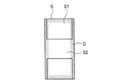
ここで、ディスクリネーション発生の一因が相互に隣接する画素間の電圧差に起因した横方向電界にあることに鑑みると、画素5’のうちディスクリネーションが発生し得る主な領域Dは当該画素5’の周縁部分(図6における斜線部分)であると考えられる。したがって、図6に示した画素5’においては、その周縁に位置する透過領域52’のみがディスクリネーションに起因して実質的に縮小される(すなわち表示に有効に寄与する領域が縮小される)こととなるため、透過領域52’の面積が反射領域51’の面積と比較して相対的に狭くなる。このように反射領域51’と透過領域52’との面積比率に偏りが生じると、表示方式によって表示品位のばらつきが生じることとなる。すなわち図6の場合を例にとると、透過型表示のときの表示画像の明るさが低下する。なお、ここではディスクリネーションが主として透過領域52’において発生する場合を想定したが、図6において反射領域51’と透過領域52’とを反転させた構成の画素においては反射領域51’のみにおいてディスクリネーションが発生するから、反射領域51’と透過領域52’との面積比率に偏りが生じるという問題は同様に生じる。
【0036】
これに対し本実施形態においては、画素5を画定する複数の縁辺のうち一部の縁辺を横切るように反射層21の形状が選定されている。したがって、画素5の周縁にディスクリネーションが発生した場合には、図7に示すように、ディスクリネーションの発生領域Dが、透過領域52と反射領域51の双方にわたることとなる。すなわち、透過領域52と反射領域51の双方において、画像表示に有効に寄与する面積(つまりディスクリネーションが発生していない領域の面積)が縮小される。このように本実施形態によれば、透過領域52および反射領域51のいずれか一方のみにおいてディスクリネーションが発生するのを避けることができるから、それぞれの表示方式において表示品位に差が生じるのを抑えることができる。
【0037】
このことからも明らかなように、ディスクリネーションに起因した表示品位のばらつきを抑えるという観点からすると、各画素5においては、反射領域51のうちディスクリネーション発生領域に相当する部分の面積と、透過領域52のうちディスクリネーション発生領域に相当する部分の面積とをほぼ等しくすることが望ましいといえる。この構成によれば、ディスクリネーションに起因して表示欠陥となる面積を反射領域51と透過領域52とにおいて等しくすることができるから、各表示方式における表示品位の差異をより確実に抑えることができる。
【0038】
<B:変形例>
以上説明した実施の形態はあくまでも本発明の一態様を示すものに過ぎず、この形態に対しては本発明の趣旨から逸脱しない範囲で様々な変形を加えることができる。変形例としては例えば以下のようなものが考えられる。
【0039】
<B−1:変形例1>
上記実施形態においては反射層21がセグメント電極22と導通する構成を例示したが、これらを導通させる必要は必ずしもない。すなわち、図8に示すように、反射層21が設けられた第2基板20の表面を樹脂材料などからなる絶縁層25によって覆うとともに、この絶縁層25の表面に、透明導電膜の単層からなるセグメント電極22を設けた構成としてもよい。
【0040】
また、上記実施形態においては第1基板10に遮光層11およびカラーフィルタ12を設けたが、第2基板20にこれらの要素を設けてもよい。すなわち、図9に示すように、反射層21が形成された第2基板20の面上に、遮光層11およびカラーフィルタ12と、これらを覆うオーバーコート層13とを形成する。そして、このオーバーコート層13の表面にセグメント電極22を形成するのである。一方、第1基板10の面上には、コモン電極14および配向膜15が設けられる。図8および図9に示した本変形例に係る構成のもとでも、反射層21の形状を図2および図5に示したものとすれば上記実施形態と同様の効果が得られる。
【0041】
<B−2:変形例2>
上記実施形態および変形例においては、緑色のカラーフィルタ12Gの透過率と、赤色のカラーフィルタ12Rおよび青色のカラーフィルタ12Bの透過率との相違を補償するために、緑色の画素5Gにおける反射領域51と透過領域52との面積比率を、赤色の画素5Rおよび青色の画素5Bにおける反射領域51と透過領域52との面積比率と異ならせるようにした。しかしながら、それぞれ異なる色の画素5ごとに、反射領域51と透過領域52との面積比率を異ならせるようにしてもよい。例えば、図3に示した例では、青色のカラーフィルタ12Bの最大透過率(約0.89)よりも赤色のカラーフィルタ12Rの最大透過率(約0.92)の方が大きい。したがって、緑色の画素5Gにおける反射領域51と透過領域52との面積比率を他の画素5の反射領域51と透過領域52との面積比率と異ならせるだけでなく、青色の画素5Bにおける反射領域51の面積を赤色の画素5Rにおける反射領域51の面積よりも大きくしてもよい。この構成によれば、緑色のカラーフィルタ12Gと赤色および青色のカラーフィルタ12Rおよび12Bとの間の透過率の相違を補償するだけでなく、赤色のカラーフィルタ12Rと青色のカラーフィルタ12Bとの間の透過率の相違をも補償することができる。
【0042】
このように、本発明においては、それぞれ異なる色に対応する複数の画素(上記実施形態においては赤色、緑色および青色にそれぞれ対応する3つの画素5R、5Gおよび5B)のうち、少なくとも一の画素における反射領域と透過領域との面積比率を他の画素における反射領域と透過領域との面積比率と異ならせる構成を採用することができる。そして、各色のカラーフィルタにおける透過率特性の相違をより確実に補償するためには、異なる色に対応する画素ごとに、反射領域と透過領域との面積比率を異ならせることが望ましいといえる。もっとも、各色のカラーフィルタ12における透過率特性の相違を補償する必要がない場合や、各色のカラーフィルタ12における透過率の相違が無視できるほど小さい場合などには、すべての画素5において反射領域51と透過領域52との面積比率(ひいては反射領域21と透過領域52との位置関係)を同一としてもよい。
【0043】
<B−3:変形例3>
上記実施形態および各変形例においては、緑色のカラーフィルタ12Gにのみ開口部121を設ける構成としたが、さらに他色のカラーフィルタ12に開口部121を設けてもよい。加えて、反射型表示のときに観察者によって視認される各色の光量のバランスを保つべく、各色のカラーフィルタ12ごとに、開口部121の面積を異ならせる構成としてもよい。この構成のもとでは、各色のカラーフィルタ12の開口部121の面積が各カラーフィルタ12における透過率の相違に応じて選定されていることが望ましい。すなわち、透過率が小さいカラーフィルタ12には大面積の開口部121を設ける一方、透過率が大きいカラーフィルタには小面積の開口部121を設けるといった具合である。
【0044】
このように本発明においては、それぞれ異なる色に対応する複数のカラーフィルタのうち少なくとも一の色のカラーフィルタにおける開口部の面積と他の色のカラーフィルタにおける開口部の面積とが、各色のカラーフィルタの透過率の相違に応じて異なるように構成することが望ましい。もっとも、カラーフィルタに開口部を設けた構成は本発明において必ずしも必要ではない。
【0045】
また、上記実施形態および各変形例においては、緑色のカラーフィルタ12Gと他色のカラーフィルタ12との透過率の相違に起因した各色の光量のばらつきを抑えるためにカラーフィルタ12Gに開口部121を設けた場合を想定したが、開口部121の有無およびその面積は、以下に示すように必ずしも各カラーフィルタ12の透過率に応じたものである必要はない。例えば、反射層21が特定の波長の光を特に多く反射させる特性を有するものである場合(つまり反射層21による反射光量が波長に応じてばらつく場合)には、表示画像が当該特定の色を帯びる場合がある。このような表示画像への色付きを抑えるために、反射光量が多い波長に近い波長の光を透過させるカラーフィルタ12が開口部121を有する構成としてもよい。例えば、黄色に対応する波長の反射光量が他の波長の反射光量よりも多い特性を有する反射層21を用いた場合には表示画像が黄色みを帯びたものとなるが、この場合には、黄色に近い波長の光を透過させる緑色のカラーフィルタ12Gに開口部121を設ければ、表示画像への色付きを抑えることができる。
【0046】
<B−4:変形例4>
上記実施形態および各変形例においては、カラーフィルタ12を備えた液晶表示パネル1を例示したが、カラーフィルタ12を備えずモノクロ表示のみを行なう液晶表示パネルにも本発明を適用することができる。この場合、第1基板10上のコモン電極14と第2基板20上のセグメント電極22との交差領域が画素(すなわちドット)に相当し、この画素内に反射領域と透過領域とが形成されることとなる。すなわち、本発明における「画素」は、それが表示画像の最小単位たるドットに相当するか、ひとつのドットを構成する一部分(上記実施形態における画素5)に相当するかを問わず、第1基板10上の電極と第2基板20上の電極とが交差する領域、すなわち両電極間の電圧差によって液晶の配向方向が変化させられる領域を意味する。
【0047】
<B−5:変形例5>
上記実施形態および各変形例においては、パッシブマトリクス方式の液晶表示パネルを例示したが、TFD(Thin Film Diode)に代表される二端子型スイッチング素子や、TFT(Thin Film Transistor)に代表される三端子型スイッチング素子を採用したアクティブマトリクス方式の液晶表示パネルにも本発明を適用可能である。
【0048】
また、上記実施形態および各変形例においては観察側に位置する第1基板10にコモン電極14が設けられ、背面側に位置する第2基板20にセグメント電極22が設けられた構成を例示したが、これとは逆に、第1基板10にセグメント電極が設けられて第2基板20にコモン電極が設けられた構成としてもよい。このように、本発明において一方の基板上に設けられる「電極」は、他方の基板上の電極とともに液晶に対して電圧を印加するための導電層であれば足り、印加される電圧の内容やその形状の如何は不問である。
【0049】
<C:電子機器>
次に、本発明に係る液晶表示パネルを用いた電子機器について説明する。
【0050】
<C−1:モバイル型コンピュータ>
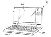
まず、本発明に係る液晶表示パネルを、可搬型のパーソナルコンピュータ(いわゆるノート型パソコン)の表示部に適用した例について説明する。図10は、このパーソナルコンピュータの構成を示す斜視図である。同図に示すように、パーソナルコンピュータ91は、キーボード911を備えた本体部912と、本発明に係る液晶表示パネルを適用した表示部913とを備えている。
【0051】
<C−2:携帯電話機>
続いて、本発明に係る液晶表示パネルを、携帯電話機の表示部に適用した例について説明する。図11は、この携帯電話機の構成を示す斜視図である。同図に示すように、携帯電話機92は、複数の操作ボタン921のほか、受話口922、送話口923とともに、本発明に係る液晶表示パネルを適用した表示部924を備える。
【0052】
なお、本発明に係る液晶表示パネルを適用可能な電子機器としては、図10に示したパーソナルコンピュータや図11に示した携帯電話機のほかにも、液晶テレビや、ビューファインダ型・モニタ直視型のビデオテープレコーダ、カーナビゲーション装置、ページャ、電子手帳、電卓、ワードプロセッサ、ワークステーション、テレビ電話、POS端末、ディジタルスチルカメラなどが挙げられる。
【0053】
【発明の効果】
以上説明したように、本発明によれば、ディスクリネーションに起因して反射領域と透過領域との面積比率に偏りが生じるのを抑えることができる。
【図面の簡単な説明】
【図1】 本発明の実施形態に係る液晶表示装置の構成を示す断面図である。
【図2】 同液晶表示パネルにおけるコモン電極、セグメント電極および反射層の位置関係を示す平面図である。
【図3】 同液晶表示パネルにおけるカラーフィルタの透過率特性を示すグラフである。
【図4】 同液晶表示パネルにおけるセグメント電極と反射層との関係を示す断面図である。
【図5】 同液晶表示パネルにおける画素、カラーフィルタおよび反射層の位置関係を示す平面図および断面図である。
【図6】 同実施形態の効果を説明するための対比例を示す図である。
【図7】 同実施形態の効果を説明するための図である。
【図8】 本発明の変形例に係る液晶表示パネルの構成を示す断面図である。
【図9】 本発明の変形例に係る液晶表示パネルの構成を示す断面図である。
【図10】 本発明に係る液晶表示パネルを適用した電子機器の一例たるパーソナルコンピュータの構成を示す斜視図である。
【図11】 本発明に係る液晶表示パネルを適用した電子機器の一例たる携帯電話機の構成を示す斜視図である。
【符号の説明】
1……液晶表示パネル、10……第1基板、11……遮光層、12(12R,12G,12B)……カラーフィルタ、121……開口部、13……オーバーコート層、14……コモン電極(電極)、15,23……配向膜、20……第2基板、21……反射層、22……セグメント電極、30……シール材、31……液晶、4……バックライトユニット、5(5R,5G,5B)……画素、51……反射領域、52……透過領域、D……ディスクリネーション発生領域、91……パーソナルコンピュータ(電子機器)、92……携帯電話機(電子機器)。[0001]
BACKGROUND OF THE INVENTION
The present invention relates to a liquid crystal display panel capable of reflective display and transmissive display, and an electronic apparatus including the liquid crystal display panel.
[0002]
[Prior art]
A so-called transflective liquid crystal display panel capable of reflective display and transmissive display is widely used as a display device for various electronic devices such as mobile phones. In general, this type of liquid crystal display panel employs a configuration in which a reflective layer having an opening is provided on the surface of the substrate on the back side of the pair of substrates that sandwich the liquid crystal. Under this configuration, external light such as sunlight and room illumination light incident from the observation side is reflected from the surface of the reflection layer and then emitted from the observation side, whereby a reflective display is realized. On the other hand, irradiation light such as a backlight unit incident from the back side passes through an opening provided in the reflective layer and is emitted to the observation side, thereby realizing a transmissive display. According to the transflective liquid crystal display panel, the backlight unit is turned off to perform reflective display in an environment where there is sufficient external light, while the backlight unit is turned on in an environment where external light is insufficient. Thus, there is an advantage that visibility of a display image can be ensured by performing transmissive display (see, for example, Patent Document 1).
[0003]
[Patent Document 1]
Japanese Patent Laid-Open No. 2002-14334 (
[0004]
[Problems to be solved by the invention]
By the way, in a liquid crystal display panel, a horizontal electric field is generated due to a voltage difference between adjacent pixels, and liquid crystal molecules are aligned in a direction different from an intended alignment direction due to the influence of the horizontal electric field. A phenomenon (hereinafter referred to as “disclination”) may occur. If the alignment direction of the liquid crystal molecules is disturbed in this way, the light is not modulated in the desired polarization direction. Therefore, in the area where the disclination occurs in each pixel, there is a significant effect on the display quality such as a decrease in color reproducibility and display defects. The trouble that can give.
[0005]
In the above-described transflective liquid crystal display panel, an area of the pixel that reflects light for reflection display (hereinafter referred to as “reflection area”) and a light of the pixel for transmission display are displayed. There is a problem that the area ratio with the region that transmits light (hereinafter referred to as “transmission region”) is different from the intended ratio due to disclination. That is, for example, when disclination occurs only in the transmissive region, the area that effectively contributes to image display in the transmissive region is substantially reduced, so that the area of the transmissive region is smaller than that of the reflective region. It is relatively narrow compared to the area. If the area ratio between the reflective region and the transmissive region is biased as described above, there may be a problem that display quality varies depending on the display method. In particular, when the area of a pixel is reduced in order to meet the demand for higher definition of a display image in recent years, the proportion of the area where the disclination occurs in each pixel relatively increases. Is even more prominent.
[0006]
The present invention has been made in view of the circumstances described above, and a liquid crystal display panel capable of suppressing a deviation in the area ratio between the reflective region and the transmissive region due to disclination, and the liquid crystal display An object is to provide an electronic device including a panel.
[0007]
[Means for Solving the Problems]
In order to solve the above problems, a feature of the present invention is that an intersection region between an electrode provided on a first substrate and an electrode provided on a second substrate facing the first substrate across a liquid crystal is used as a pixel. In the liquid crystal display panel in which the pixels are arranged in a matrix form in the X and Y directions, the reflective layer is provided on the second substrate and reflects incident light from the first substrate side. A reflective region that reflects incident light from the first substrate side by a reflective layer; and a transmissive region that transmits incident light from the second substrate side to the first substrate side of the pixel, Is a substantially rectangular shape, and the reflection region is provided at both edge ends in the Y direction of the periphery of the pixel, and the transmission region is a region sandwiched between the reflection regions in the pixel. The reflection layer reflects the incident light from the first substrate side, the area corresponding to the disclination generation region, and the incident light from the second substrate side on the first substrate side. The area corresponding to the disclination generation area is substantially equal to the transmission area to be transmitted through There is.
[0008]
According to this configuration, since the reflective layer is provided so as to cross a part of the periphery of the pixel, the reflective region of the pixel that reflects incident light from the first substrate side by the reflective layer, and the pixel Among them, a transmission region that transmits incident light from the second substrate side to the first substrate side is adjacent along the periphery of the pixel. Therefore, when disclination occurs along the periphery of the pixel, the region where the disclination occurs extends over both the reflection region and the transmission region. As a result, it is possible to avoid the occurrence of disclination in only one of the reflective region and the transmissive region, so that the area ratio between the reflective region and the transmissive region is biased due to disclination. Can be suppressed.
[0011]
Up In the liquid crystal display panel according to the present invention having the features described above Is The area that causes display defects due to disclination is the same in the reflective and transmissive areas. No Therefore, the difference between the display quality in the reflective display and the display quality in the transmissive display can be more reliably suppressed.
[0013]
On the other hand, a liquid crystal display panel having a plurality of pixels each assigned a different color, that is, provided on the observation side of the reflective layer so as to overlap each pixel, and selectively emits light having a wavelength corresponding to the color of the pixel. When the present invention is applied to a liquid crystal display panel having a plurality of color filters to transmit, at least one pixel among the plurality of pixels corresponding to different colors and the other pixels by the reflective layer. The area ratio between the reflection region that reflects incident light from the first substrate side and the transmission region that transmits incident light from the second substrate side to the first substrate side may be different. According to this configuration, it is possible to arbitrarily set the amount of light reflected from the surface of the reflective layer and emitted to the observation side for each color pixel in the reflective display. Therefore, for example, if the area ratio between the reflective region and the transmissive region in each color pixel is selected according to the transmittance of each color filter, it is possible to compensate for the variation in transmittance for each color and realize good color reproducibility. Can do. In addition, for example, even when the light irradiated by the backlight unit has a variation in spectral characteristics (that is, when the amount of light of each wavelength is different), the area ratio between the reflective region and the transmissive region in each pixel is changed to this spectral characteristic. If the selection is made accordingly, it is possible to compensate for variations in spectral characteristics and realize good color reproducibility.
[0014]
In addition, as the color filter of at least one color among the plurality of color filters, a pixel having an opening in a region overlapping with the reflective layer among the pixels corresponding to the color filter may be used. According to this configuration, the amount of light transmitted through the color filter and emitted to the observation side in the reflective display can be arbitrarily set according to the area of the opening. Furthermore, in a liquid crystal display panel in which an opening is provided in the color filter, the area of the opening of the color filter of at least one color may be different from the area of the opening of the color filter of another color. By so doing, it is possible to realize good color reproducibility by compensating for the difference in transmittance of the color filters of the respective colors.
[0015]
An electronic apparatus according to the present invention includes the liquid crystal display panel according to the present invention as a display device. As described above, according to the liquid crystal display panel according to the present invention, it is possible to suppress a deviation in the area ratio between the reflective region and the transmissive region due to disclination. The display device is particularly suitable as a display device mounted on an electronic device that can switch between a mold display and a transmissive display and requires high display quality in both display methods. As such an electronic device, for example, a portable personal computer or a mobile phone can be considered.
[0016]
DETAILED DESCRIPTION OF THE INVENTION
Embodiments of the present invention will be described below with reference to the drawings. In the drawings shown below, the dimensions and ratios of the constituent elements are appropriately changed from the actual ones in order to prevent the drawings from becoming complicated.
[0017]
<A: Configuration of Embodiment>
First, an embodiment in which the present invention is applied to a passive matrix type transflective liquid crystal display panel will be described with reference to FIG. As shown in the figure, the liquid crystal display device according to this embodiment includes a liquid crystal display panel 1 and a
[0018]
The
[0019]
On the other hand, the
[0020]
A plurality of
[0021]
On the other hand, a plurality of
[0022]
The alignment direction of the
[0023]
As shown in FIG. 1, a
[0024]
Next, the color filter 12 (12R, 12G, and 12B) is a resin layer formed corresponding to each
[0025]
Here, FIG. 3 is a diagram illustrating the transmittance characteristics of the
[0026]
On the other hand, as shown in FIGS. 1 and 2, a plurality of
[0027]
Here, FIG. 4 is a diagram showing a positional relationship between the
[0028]
On the other hand, as shown in FIG. 2, focusing on a plane parallel to the plate surface of the
[0029]
On the other hand, an area (hereinafter referred to as “transmission area”) 52 other than the area covered by the
[0030]
Next, a more detailed configuration of the
[0031]
On the other hand, as shown in FIG. 2, the
[0032]
Next, the shape of the
[0033]
Thus, in the present embodiment, the shape of the
[0034]
Now, for the purpose of comparison with the present embodiment, it is assumed that the
[0035]
Here, considering that the cause of disclination is the horizontal electric field caused by the voltage difference between adjacent pixels, the main region D in which disclination can occur in the
[0036]
On the other hand, in the present embodiment, the shape of the
[0037]
As is clear from this, from the viewpoint of suppressing variation in display quality due to disclination, in each
[0038]
<B: Modification>
The embodiment described above merely shows one aspect of the present invention, and various modifications can be made to this embodiment without departing from the spirit of the present invention. As modifications, for example, the following can be considered.
[0039]
<B-1: Modification 1>
In the above-described embodiment, the configuration in which the
[0040]
In the above embodiment, the
[0041]
<B-2: Modification 2>
In the embodiment and the modification, the
[0042]
Thus, in the present invention, at least one pixel among a plurality of pixels corresponding to different colors (in the above-described embodiment, the three
[0043]
<B-3: Modification 3>
In the embodiment and each modification, the
[0044]
Thus, in the present invention, the area of the opening in the color filter of at least one color among the plurality of color filters corresponding to different colors and the area of the opening in the color filter of the other color are the colors of each color. It is desirable to configure differently depending on the difference in transmittance of the filter. However, a configuration in which an opening is provided in the color filter is not necessarily required in the present invention.
[0045]
Further, in the above-described embodiment and each modification, an
[0046]
<B-4:
In the above embodiment and each modification, the liquid crystal display panel 1 including the
[0047]
<B-5:
In the above embodiment and each modified example, a passive matrix type liquid crystal display panel is exemplified, but a two-terminal switching element represented by TFD (Thin Film Diode) and three represented by TFT (Thin Film Transistor). The present invention can also be applied to an active matrix liquid crystal display panel that employs terminal-type switching elements.
[0048]
Moreover, in the said embodiment and each modification, although the
[0049]
<C: Electronic equipment>
Next, electronic devices using the liquid crystal display panel according to the present invention will be described.
[0050]
<C-1: Mobile computer>
First, an example in which the liquid crystal display panel according to the present invention is applied to a display unit of a portable personal computer (so-called notebook personal computer) will be described. FIG. 10 is a perspective view showing the configuration of this personal computer. As shown in the figure, the
[0051]
<C-2: Mobile phone>
Next, an example in which the liquid crystal display panel according to the present invention is applied to a display unit of a mobile phone will be described. FIG. 11 is a perspective view showing the configuration of the mobile phone. As shown in the figure, the
[0052]
In addition to the personal computer shown in FIG. 10 and the mobile phone shown in FIG. 11, electronic devices to which the liquid crystal display panel according to the present invention can be applied include a liquid crystal television, a viewfinder type, and a monitor direct view type. Examples include a video tape recorder, a car navigation device, a pager, an electronic notebook, a calculator, a word processor, a workstation, a video phone, a POS terminal, and a digital still camera.
[0053]
【The invention's effect】
As described above, according to the present invention, it is possible to suppress the occurrence of deviation in the area ratio between the reflective region and the transmissive region due to disclination.
[Brief description of the drawings]
FIG. 1 is a cross-sectional view showing a configuration of a liquid crystal display device according to an embodiment of the present invention.
FIG. 2 is a plan view showing a positional relationship among a common electrode, a segment electrode, and a reflective layer in the liquid crystal display panel.
FIG. 3 is a graph showing transmittance characteristics of a color filter in the liquid crystal display panel.
FIG. 4 is a cross-sectional view showing a relationship between a segment electrode and a reflective layer in the liquid crystal display panel.
FIGS. 5A and 5B are a plan view and a cross-sectional view showing a positional relationship among pixels, a color filter, and a reflective layer in the liquid crystal display panel.
FIG. 6 is a diagram showing a comparison for explaining the effect of the embodiment;
FIG. 7 is a diagram for explaining the effect of the embodiment.
FIG. 8 is a cross-sectional view showing a configuration of a liquid crystal display panel according to a modification of the present invention.
FIG. 9 is a cross-sectional view showing a configuration of a liquid crystal display panel according to a modification of the present invention.
FIG. 10 is a perspective view showing a configuration of a personal computer as an example of an electronic apparatus to which the liquid crystal display panel according to the present invention is applied.
FIG. 11 is a perspective view showing a configuration of a mobile phone as an example of an electronic apparatus to which the liquid crystal display panel according to the present invention is applied.
[Explanation of symbols]
DESCRIPTION OF SYMBOLS 1 ... Liquid crystal display panel, 10 ... 1st board | substrate, 11 ... Light shielding layer, 12 (12R, 12G, 12B) ... Color filter, 121 ... Opening part, 13 ... Overcoat layer, 14 ... Common Electrodes (electrodes) 15, 23... Alignment film, 20... Second substrate, 21... Reflective layer, 22 ... Segment electrode, 30 ... Seal material, 31 ... Liquid crystal, 4 ... Backlight unit, 5 (5R, 5G, 5B): Pixel, 51: Reflection area, 52: Transmission area, D: Disclination generation area, 91: Personal computer (electronic device), 92: Mobile phone (electronic) machine).
Claims (6)
前記第2基板に設けられて前記第1基板側からの入射光を反射させる反射層であって、前記画素のうち当該反射層によって前記第1基板側からの入射光を反射させる反射領域と、
当該画素のうち前記第2基板側からの入射光を前記第1基板側に透過させる透過領域と
を有し、
前記画素は、略矩形状であり、
前記反射領域は、前記画素の周縁のうち、前記Y方向の両縁端部に設けられ、
前記透過領域は、前記画素における反射領域で挟まれた領域であり、
前記反射層によって前記第1基板側からの入射光を反射させる反射領域のうちディスクリネーション発生領域に相当する部分の面積と、前記第2基板側からの入射光を前記第1基板側に透過させる透過領域のうち当該ディスクリネーション発生領域に相当する部分の面積とが略等しい
ことを特徴とする液晶表示パネル。An intersection region between the electrode provided on the first substrate and the electrode provided on the second substrate facing the first substrate across the liquid crystal is used as a pixel, and the pixels are arranged in a matrix in the X and Y directions. In the liquid crystal display panel,
A reflective layer provided on the second substrate for reflecting incident light from the first substrate side, wherein the reflective layer of the pixels reflects incident light from the first substrate side by the reflective layer;
A transmission region that transmits incident light from the second substrate side to the first substrate side of the pixel,
The pixel has a substantially rectangular shape,
The reflective area is provided at both edge ends in the Y direction among the peripheral edges of the pixel,
The transmissive region, Ri region der sandwiched between the reflection area of the pixel,
Of the reflective region that reflects the incident light from the first substrate side by the reflective layer, the area corresponding to the disclination generation region and the incident light from the second substrate side are transmitted to the first substrate side. A liquid crystal display panel, characterized in that an area of a portion corresponding to the disclination generation region in the transmissive region is substantially equal .
ことを特徴とする請求項1に記載の液晶表示パネル。The liquid crystal display panel according to claim 1 , wherein the reflective layer has conductivity and is electrically connected to an electrode provided on the second substrate.
前記反射層よりも観察側において前記各画素と重なるように設けられて当該画素の色に対応する波長の光を選択的に透過させる複数のカラーフィルタを具備し、
それぞれ異なる色に対応する前記複数の画素のうち少なくとも一の画素と他の画素とにおいて、前記反射層によって前記第1基板側からの入射光を反射させる反射領域と前記第2基板側からの入射光を前記第1基板側に透過させる透過領域との面積比率が異なる
ことを特徴とする請求項1に記載の液晶表示パネル。A liquid crystal display panel having a plurality of the pixels each assigned a different color,
A plurality of color filters provided so as to overlap each pixel on the observation side of the reflective layer and selectively transmitting light having a wavelength corresponding to the color of the pixel;
In at least one pixel and other pixels among the plurality of pixels corresponding to different colors, a reflection region for reflecting incident light from the first substrate side by the reflection layer and incidence from the second substrate side 2. The liquid crystal display panel according to claim 1, wherein an area ratio of a transmission region that transmits light to the first substrate side is different.
ことを特徴とする請求項3に記載の液晶表示パネル。4. The liquid crystal according to claim 3 , wherein a color filter of at least one color among the plurality of color filters has an opening in a region overlapping the reflective layer in the pixel corresponding to the color filter. Display panel.
ことを特徴とする請求項4に記載の液晶表示パネル。The liquid crystal display panel according to claim 4 , wherein an area of the opening of the color filter of at least one color is different from an area of the opening of the color filter of another color.
Priority Applications (1)
| Application Number | Priority Date | Filing Date | Title |
|---|---|---|---|
| JP2002280872A JP4165165B2 (en) | 2002-09-26 | 2002-09-26 | Liquid crystal display panel and electronic equipment |
Applications Claiming Priority (1)
| Application Number | Priority Date | Filing Date | Title |
|---|---|---|---|
| JP2002280872A JP4165165B2 (en) | 2002-09-26 | 2002-09-26 | Liquid crystal display panel and electronic equipment |
Publications (3)
| Publication Number | Publication Date |
|---|---|
| JP2004117815A JP2004117815A (en) | 2004-04-15 |
| JP2004117815A5 JP2004117815A5 (en) | 2005-10-06 |
| JP4165165B2 true JP4165165B2 (en) | 2008-10-15 |
Family
ID=32275465
Family Applications (1)
| Application Number | Title | Priority Date | Filing Date |
|---|---|---|---|
| JP2002280872A Expired - Fee Related JP4165165B2 (en) | 2002-09-26 | 2002-09-26 | Liquid crystal display panel and electronic equipment |
Country Status (1)
| Country | Link |
|---|---|
| JP (1) | JP4165165B2 (en) |
Families Citing this family (10)
| Publication number | Priority date | Publication date | Assignee | Title |
|---|---|---|---|---|
| US8362987B2 (en) | 2004-09-27 | 2013-01-29 | Qualcomm Mems Technologies, Inc. | Method and device for manipulating color in a display |
| RU2507549C2 (en) * | 2004-09-27 | 2014-02-20 | Квэлкомм Мемс Текнолоджиз, Инк. | Method and apparatus for controlling colour on display |
| US7525730B2 (en) | 2004-09-27 | 2009-04-28 | Idc, Llc | Method and device for generating white in an interferometric modulator display |
| US8031133B2 (en) | 2004-09-27 | 2011-10-04 | Qualcomm Mems Technologies, Inc. | Method and device for manipulating color in a display |
| US7710632B2 (en) | 2004-09-27 | 2010-05-04 | Qualcomm Mems Technologies, Inc. | Display device having an array of spatial light modulators with integrated color filters |
| US8102407B2 (en) | 2004-09-27 | 2012-01-24 | Qualcomm Mems Technologies, Inc. | Method and device for manipulating color in a display |
| US7911428B2 (en) | 2004-09-27 | 2011-03-22 | Qualcomm Mems Technologies, Inc. | Method and device for manipulating color in a display |
| US8004743B2 (en) | 2006-04-21 | 2011-08-23 | Qualcomm Mems Technologies, Inc. | Method and apparatus for providing brightness control in an interferometric modulator (IMOD) display |
| US8848294B2 (en) | 2010-05-20 | 2014-09-30 | Qualcomm Mems Technologies, Inc. | Method and structure capable of changing color saturation |
| KR102515963B1 (en) * | 2016-03-04 | 2023-03-30 | 삼성디스플레이 주식회사 | Organic light emitting display panel |
-
2002
- 2002-09-26 JP JP2002280872A patent/JP4165165B2/en not_active Expired - Fee Related
Also Published As
| Publication number | Publication date |
|---|---|
| JP2004117815A (en) | 2004-04-15 |
Similar Documents
| Publication | Publication Date | Title |
|---|---|---|
| US7030946B2 (en) | Liquid crystal display device, substrate assembly for liquid crystal display device, and electronic apparatus having a substantially equivalent display quality in both transmissive and reflective display modes | |
| JP3674581B2 (en) | Color filter substrate, manufacturing method thereof, liquid crystal display panel, and electronic device | |
| JP3941548B2 (en) | Liquid crystal display panel, liquid crystal display panel substrate and electronic device | |
| JP2003195296A (en) | Liquid crystal display device and electronic apparatus | |
| JP3534097B2 (en) | Liquid crystal device and electronic equipment provided with the liquid crystal device | |
| JP4165165B2 (en) | Liquid crystal display panel and electronic equipment | |
| JP2003255324A (en) | Liquid crystal display panel, substrate for liquid crystal display panel and electronic equipment | |
| US7639326B2 (en) | Liquid crystal device and electronic apparatus | |
| JP2006184379A (en) | Electro-optical device, color filter substrate and electronic equipment | |
| JP2002055333A (en) | Substrate for liquid crystal device, method for manufacturing the same, liquid crystal device and electronic appliance | |
| JP4254092B2 (en) | Liquid crystal display panel and electronic equipment | |
| JP5175122B2 (en) | Liquid crystal display device and electronic device | |
| JP4042540B2 (en) | Color filter substrate, manufacturing method thereof, liquid crystal display panel, and electronic device | |
| JP4075903B2 (en) | Liquid crystal display panel, liquid crystal display panel substrate and electronic device | |
| JP2002229009A (en) | Liquid crystal display and electronic device | |
| JP4052311B2 (en) | Color filter substrate, manufacturing method thereof, liquid crystal display panel, and electronic device | |
| JP2005134544A (en) | Liquid crystal display device and electronic apparatus | |
| JP2006234999A (en) | Electrooptical device and electronic equipment | |
| JP4335158B2 (en) | Color filter substrate, manufacturing method thereof, liquid crystal display panel, and electronic device | |
| JP4645327B2 (en) | Liquid crystal display device and electronic device | |
| JP2002229010A (en) | Liquid crystal display and electronic device | |
| JP3617520B2 (en) | Liquid crystal device | |
| JP4042758B2 (en) | Liquid crystal device and electronic device | |
| JP2006064732A (en) | Liquid crystal display and display device | |
| JP2002229011A (en) | Liquid crystal display and electronic device |
Legal Events
| Date | Code | Title | Description |
|---|---|---|---|
| A521 | Written amendment |
Free format text: JAPANESE INTERMEDIATE CODE: A523 Effective date: 20050525 |
|
| A621 | Written request for application examination |
Free format text: JAPANESE INTERMEDIATE CODE: A621 Effective date: 20050525 |
|
| A977 | Report on retrieval |
Free format text: JAPANESE INTERMEDIATE CODE: A971007 Effective date: 20080104 |
|
| A131 | Notification of reasons for refusal |
Free format text: JAPANESE INTERMEDIATE CODE: A131 Effective date: 20080115 |
|
| A521 | Written amendment |
Free format text: JAPANESE INTERMEDIATE CODE: A523 Effective date: 20080310 |
|
| A131 | Notification of reasons for refusal |
Free format text: JAPANESE INTERMEDIATE CODE: A131 Effective date: 20080507 |
|
| A521 | Written amendment |
Free format text: JAPANESE INTERMEDIATE CODE: A523 Effective date: 20080605 |
|
| TRDD | Decision of grant or rejection written | ||
| A01 | Written decision to grant a patent or to grant a registration (utility model) |
Free format text: JAPANESE INTERMEDIATE CODE: A01 Effective date: 20080708 |
|
| A01 | Written decision to grant a patent or to grant a registration (utility model) |
Free format text: JAPANESE INTERMEDIATE CODE: A01 |
|
| A61 | First payment of annual fees (during grant procedure) |
Free format text: JAPANESE INTERMEDIATE CODE: A61 Effective date: 20080721 |
|
| R150 | Certificate of patent or registration of utility model |
Free format text: JAPANESE INTERMEDIATE CODE: R150 |
|
| FPAY | Renewal fee payment (event date is renewal date of database) |
Free format text: PAYMENT UNTIL: 20110808 Year of fee payment: 3 |
|
| FPAY | Renewal fee payment (event date is renewal date of database) |
Free format text: PAYMENT UNTIL: 20120808 Year of fee payment: 4 |
|
| FPAY | Renewal fee payment (event date is renewal date of database) |
Free format text: PAYMENT UNTIL: 20130808 Year of fee payment: 5 |
|
| S531 | Written request for registration of change of domicile |
Free format text: JAPANESE INTERMEDIATE CODE: R313531 |
|
| R350 | Written notification of registration of transfer |
Free format text: JAPANESE INTERMEDIATE CODE: R350 |
|
| LAPS | Cancellation because of no payment of annual fees |