JP4162165B2 - Quantum well structure optical semiconductor device - Google Patents
Quantum well structure optical semiconductor device Download PDFInfo
- Publication number
- JP4162165B2 JP4162165B2 JP22916298A JP22916298A JP4162165B2 JP 4162165 B2 JP4162165 B2 JP 4162165B2 JP 22916298 A JP22916298 A JP 22916298A JP 22916298 A JP22916298 A JP 22916298A JP 4162165 B2 JP4162165 B2 JP 4162165B2
- Authority
- JP
- Japan
- Prior art keywords
- layer
- quantum well
- group
- quantum
- type
- Prior art date
- Legal status (The legal status is an assumption and is not a legal conclusion. Google has not performed a legal analysis and makes no representation as to the accuracy of the status listed.)
- Expired - Fee Related
Links
Images


Landscapes
- Semiconductor Lasers (AREA)
Description
【0001】
【発明の属する技術分野】
本発明は、長波長帯半導体レーザ素子に関する。特に、家庭へ高速のデータ配送を行うための光ファイバー通信いわゆるFTTH(Fiber To The Home)、及びコンピューターのボード間通信いわゆる光インターコネクションに用いられる、高温環境下での低閾値電流及び低駆動電流特性が要求される長波長帯半導体レーザ素子に関する。
【0002】
【従来の技術】
光ファイバーを使用した光通信システムあるいは光インターコネクションの光源として、従来はInP基板上に形成されたInGaAsP系の長波長帯半導体レーザ素子が開発されている。しかし、この半導体レーザ素子において、活性層とクラッド層との間の電子に対するバンド不連続差(エネルギーギャップの差)ΔEcが約100meVと小さいため、高温動作時に電子を活性層に十分に閉じ込めることができず、いわゆるキャリアのオーバーフローが生じるという問題があった。これが原因で、上記の半導体レーザ素子としては、温度特性が約50K程度のものしか得られなかった。
【0003】
このため、厳しい環境温度で上記の半導体レーザ素子を用いる場合、高温での動作電流が高くなることにより、駆動回路の高い出力が必要とされる。この結果、回路構成が非常に複雑となったり、レーザ素子を冷却するための装置が必要とされたりして、光通信装置の大型化、消費電力の増大等の問題が生じていた。
【0004】
上記の温度特性の問題を改善するために、InP基板上に活性層としてInGaAlAsを用いた半導体レーザ素子、及びInP基板上に活性層としてInAsPを用いた半導体レーザ素子が開発されているが、未だ実用上十分なものは得られていない。
【0005】
一方、上記の温度特性を改善するために、GaAs基板上に、GaInNAsによって量子井戸層が形成される半導体レーザ素子が提案されている(特開平8-195522号公報)。この半導体レーザ素子では、1.3〜1.7μmの長波長帯の光を発振でき、かつ150K程度の温度特性が期待できる。なお、量子井戸構造の量子障壁層は、(Al)GaAs層、またはInGaP層とGaAs層との多層構造によって構成されている(特開平8-195522号公報の実施例4〜6)。
【0006】
以下に、上記のGaInNAs系半導体レーザ素子の構造と物性との関係についてより詳細に説明する。
【0007】
図7は、GaInNAs系材料の、In及びNの組成と格子定数またはバンドギャップとの関係を示す。この図から分かるように、GaInAsの材料への窒素を添加することにより得られるGaInNAs系混晶は、添加量に応じて格子定数がGaInAsの格子定数より小さくなり、GaAsの格子定数に徐々に近づく(GaAsに格子整合する方向に変化する)。また、窒素に対するエネルギーギャップの大きいボーイングの効果により、伝導帯のバンド端のエネルギー準位はA→B→Cと、価電子帯のバンド端のエネルギー準位はD→E→Fとそれぞれ変化することで、バンドギャップEgが小さくなる。
【0008】
上記のことから、GaInNAs系材料を用いて、その中のインジウム及び窒素の組成を適切に選ぶことにより、GaAsのエネルギーギャップ1.42eV(λ:873μm)よりも小さなエネルギーギャップ、即ち1.3〜1.7μm帯の長波長帯で発振し、かつGaAs基板上に格子整合する材料が得られることがわかる。
【0009】
さらに、GaInNAs系材料の場合GaAs基板を用いることができるので、従来の素子構造で使用されているInPクラッド層に比べてバンドギャップの大きいAlGaAs層をクラッド層に使用できる。このため、バンド不連続差を大きくとることができ、温度特性として約150K程度のレーザ素子を得ることが期待できる。
【0010】
図8は、GaInNAs系材料を使用した単一量子井戸構造を有する半導体レーザ素子の構造の一例を示す(第58回応用物理学会学術講演会講演予稿集2p-ZC-4 1997年10月)。この半導体レーザ素子は、n型GaAs基板700上に、n型AlGaAs下部クラッド層704、n型GaAs下部光導波路層705(厚さ、140nm)、GaInNAs量子井戸層706(厚さ、7nm)、p型GaAs上部光導波路層707(厚さ、140nm)、p型AlGaAs上部クラッド層708、及びp型GaAsキャップ層718がこの順で形成されている。なお、基板700の裏面及びキャップ層718の上には、それぞれn側電極720及びp側電極722が設けられている。
【0011】
7nmの厚さを有するGaInNAs量子井戸層706は、GaAs基板に対して1.0%の歪みを有する。上記の構造で、共振器長800μmの場合、閾値が約103mA、発振波長が約1.3μmのレーザ素子が得られる。
【0012】
【発明が解決しようとする課題】
特開平8-195522号公報に開示されている半導体レーザ素子において、活性領域を構成する量子井戸構造は、量子井戸層としてGaInNAs層が用いられ、量子障壁層としては(Al)GaAs層またはInGaP層とGaAs層との多層構造が用いられている。しかし、このような量子井戸構造では、十分良好な素子特性が得られないという問題がある。
【0013】
上記問題の主な原因は、GaInNAs層のような窒素を含む層と、(Al)GaAs層等のような窒素を含まない層との間に、良好なヘテロ界面を形成することが困難であることにあると考えられる。
【0014】
窒素及び窒素以外のV族元素を含むIII−V族化合物半導体(以下では、N系半導体と略す)材料は、その1つの特徴として高い混合不安定性、すなわち、相分離しやすい性質を有する。GaInNAs系量子井戸構造を有するレーザ素子を形成する場合、従来によれば、(Al)GaAs量子障壁層という窒素を含まない化合物半導体層上に、量子井戸層を形成するためのN系半導体層を、またはN系半導体上に(Al)GaAsなどによる量子障壁層を成長する必要がある。この成長の途中特に成長初期に、N系半導体の上記の混合不安定性に起因して、窒素を含む半導体層上に窒素を含まない半導体層を形成する時、V族元素としてAsしか供給されないため、表面における窒素が局在化することで相分離が発生しやすくなり、良好なヘテロ界面を形成することが困難である。さらに、窒素を含まない化合物半導体上に均一な組成のN系半導体を構成することが困難ということにより、界面近傍の組成が遷移することによる遷移層が形成され、組成の急峻な界面が得られないという問題もある。
【0015】
また、N系半導体材料は、上記の混合不安定性以外に、エネルギーギャップについての高い窒素依存性を有する。すなわち、N系半導体材料のエネルギーギャップの値は、窒素の濃度に強く影響される。例えば、インジウム混晶比が0.01変化しても、N系半導体材料のエネルギーギャップは約0.01eV、格子定数で約0.007%程度しか変化しない。ところが、窒素混晶比がわずか0.01変化するだけで、N系半導体のエネルギーギャップは約0.15eV、格子定数は約0.21%程度も変化する。これは、N系半導体の窒素含有量に対するエネルギーギャップ等のボーイングは、非常に大きいためである。このことから、窒素を含む層と窒素を含まない層とで量子井戸構造を形成する場合は、窒素源の急峻な切り替えを行わない限りは、エネルギーギャップの急峻な構造を持つ量子井戸層は得られない。
【0016】
さらに、窒素を含む層と窒素を含まない層とを連続的に成長させる場合は、成長途中で、基板温度を変える必要がある。より具体的には、GaInAsN井戸層を成長させる場合は、窒素の取り込み量を増加させるために、500℃程度の低温成長が必要である。一方、Ga(Al)As障壁層を成長させる場合は、結晶性を向上させるために700℃程度の高温条件が必要である。このように、GaInAsN量子井戸層の成長からGa(Al)As量子障壁層の成長に切り替える時に、基板温度を変えなければならない。この時点で、量子井戸層表面における蒸気圧の高い元素が再蒸発するか、あるいは成長室内に残存するC、Oまたは水分などの残留不純物が量子井戸層の表面に吸着されることが生じる。このため、量子井戸層界面部の結晶性が劣化し、さらに、量子井戸層の表面状態の変化により相分離あるいはクラスタリングが発生しやすくなる。その結果、良好な結晶性及び急峻性を有するヘテロ界面を形成することが困難になる。
【0017】
上記のように、窒素を含む層と窒素を含まない層とで量子井戸構造を形成する場合、量子井戸層と量子障壁層との界面での非発光再結合の割合の増大、及び量子効果の低減によって、閾値が上昇しスロープ効率が低下する。このため、図9に示されるように、共振器内部に損失が少ない構造、いわゆる実屈折率構造であるにも関わらず、室温での電流−光特性のスロープ効率が、通常の実屈折率構造の場合(〜0.4W/A)に比べて、0.16W/Aと非常に低いものしか得られない。
【0018】
さらに、温度特性が良好であるという特徴を有するにも関わらず、スロープ効率が良くないことに起因して、高温動作時の駆動電流が高くなり回路構成が複雑になる。上記の半導体レーザ素子に対して信頼性試験を行った結果、素子寿命が5000時間程度のものしか得られないことが分かった。
【0019】
上記のように、従来技術によれば、界面での非発光再結合の増大及び量子効果の低減による、閾値の上昇やスロープ効率の低減に起因して、良好な素子特性を有する半導体レーザ素子が得られていなかった。
【0020】
本発明は、上記事情に鑑みてなされたものであって、その目的とするところは、量子井戸層と量子障壁層との界面部の結晶性が向上し、バンド構造が最適化されさらにその設計の自由度が向上した、高いスロープ効率及び低い閾値を有する量子井戸構造光半導体素子を提供することにある。
【0021】
【課題を解決するための手段】
本発明による III −V族化合物半導体レーザは、 III 族元素、及び窒素を含む2種類以上のV族元素によって形成された量子障壁層と、 III 族元素、及び窒素を含む2種類以上のV族元素によって形成された量子井戸層とを有する活性領域を備えた III −V族化合物半導体レーザであって、該活性領域とクラッド層との間に、 III 族元素、及び窒素を含む2種類以上のV族元素によって形成された光導波路層が設けられており、該光導波路層は、該量子障壁層のエネルギーギャップおよび該クラッド層のエネルギーギャップの中間のエネルギーギャップを有しており、該光導波路層のエネルギーギャップは、該量子障壁層から該クラッド層に向かって大きくなっており、そのことにより上記目的が達成される。
前記光導波路層のエネルギーギャップは、前記量子障壁層から前記クラッド層に向かって滑らかに大きくなっていてもよい。
前記光導波路層のエネルギーギャップは、前記量子障壁層から前記クラッド層に向かって段階的に大きくなっていてもよい。
前記 III 族元素は、Al、Ga、In及びTlを含む群から選択され、前記V族元素は、前記窒素以外にAs、P及びSbを含む群から選択されてもよい。
【0028】
【発明の実施の形態】
(第1の実施形態)
図1(a)及び(b)を参照しながら、本発明による量子井戸構造光半導体素子の第1の実施形態である埋め込み型の半導体レーザ素子を説明する。
【0029】
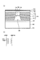
この半導体レーザ素子は、図1(a)に示されるように、p型GaAs基板100と、p型GaAsバッファー層102と、p型Al0.3Ga0.7As下部クラッド層104と、量子井戸構造106(活性領域)と、n型Al0.3Ga0.7As第1の上部クラッド層108と、電流狭窄構造110と、n型Al0.3Ga0.7As第2の上部クラッド層116と、n型GaAsキャップ層118と、を備えている。
【0030】
本発明による半導体レーザ素子の量子井戸構造106は、図1(b)に示されるように、アンドープGa0.80In0.20N0.022As0.978量子井戸活性層106aと、アンドープGa0.98In0.02N0.024As0.976量子障壁層106bと、による3周期の積層構造を有する。量子井戸活性層106aは、GaAs基板100に対して1.0%の圧縮歪みを有し、約6nmの厚さを持つ。量子井戸活性層106aは、エネルギーギャップが約0.886eVであり、格子定数が約5.710Åである。一方、量子障壁層106bは、GaAs基板100に対して0.25%の引っ張り歪みを有し、約12nmの厚さを持つ。量子障壁層106bは、エネルギーギャップが約1.03eVであり、格子定数が5.667Åである。
【0031】
また、電流狭窄構造110は、下部クラッド層104、量子井戸構造106及び第1の上部クラッド層108によって構成されるメサ構造109の両側に設けられている。電流狭窄構造110は、GaAs基板100に格子整合するn型InGaP層112と、p型InGaP層113と、n型InGaP層114と、を含んでいる。
【0032】
なお、基板100の裏面にp側電極120が形成され、n型GaAsキャップ層118上にn側電極122が形成されている。
【0033】
以下に、上記の半導体レーザ素子の製造工程を説明する。
【0034】
この製造工程において、III族元素の原料として、ガリウム、インジウム及びアルミニウム等の固体原料を用い、V族元素の原料としては砒素等の固体原料及びアンモニアを用いる。なお、n型不純物の原料としてシリコンを用い、p型不純物の原料としてはベリリウムを用いる。
【0035】
まず、650℃の基板温度で、MBE(分子線エピタキシー)法により、p型GaAs基板100上に、約0.3μm厚のp型GaAsバッファー層102と、約1.0μm厚のp型Al0.3Ga0.7As下部クラッド層104と、を順次形成する。
【0036】
続いて、砒素抜けを防止するために、砒素フラックスを照射しながら基板温度をGaInNAs層の最適成長温度である500℃程度に降温し、下部クラッド層104上に、アンドープGa0.80In0.20N0.022As0.978量子井戸活性層106aと、アンドープGa0.98In0.02N0.024As0.976量子障壁層106bと、を3周期積層して、量子井戸構造106を形成する。
【0037】
その後、V族元素の原料である砒素フラックス及びアンモニアを供給しつつ、基板温度を650℃程度に昇温した後、1.0μm厚のn型Al0.3Ga0.7As第1の上部クラッド層108、及びn型GaAs保護層(図1(a)に図示せず)を形成する。
【0038】
続いて、通常のフォトリソ工程により、ストライプ状のSiN膜による誘電体マスクをn型GaAs保護層上に形成する。次に、ウエットエッチングプロセスにて、バッファー層102の一部の表面が露出するように、下部クラッド層104、量子井戸構造106、第1の上部クラッド層108及びn型GaAs保護層を選択的にエッチングし、1.5μm幅のメサ構造109を形成する。
【0039】
さらに、MOCVD法により、誘電体マスクを利用して選択成長を行うことによって、メサ構造109の両側の露出しているバッファー層102の表面に、GaAs基板100に格子整合するn型InGaP層112(厚さ、約0.6μm)、p型InGaP層113(厚さ、約1μm)、及びn型InGaP層114(厚さ、約1μm)を順次形成する。n型InGaP層112、p型InGaP層113、及びn型InGaP層114によって、横方向において光を閉じ込め、かつ電流を狭窄する電流狭窄構造110が形成される。
【0040】
続いて、上記の誘電体マスクを除去した後、MBE法により、メサ構造109及び電流狭窄構造110上に、n型Al0.3Ga0.7As第2の上部クラッド層116、及びn型GaAsキャップ層118を順次形成する。
【0041】
最後に、基板100の裏面及びキャップ層118の上面に、それぞれp側電極120及びn側電極122を形成する。こうして、埋め込み型の半導体レーザ素子が得られる。
【0042】
上記の構成において、量子井戸活性層106aの格子定数Awellが量子障壁層106bの格子定数Abarrierより大きく設定されている。これにより、図7に示されるように、量子井戸層内に電子と正孔を閉じ込める構造が形成できる。
【0043】
本実施形態によると、量子井戸活性層106a及び量子障壁層106bは、共に窒素を含む半導体によって形成されている。このため、窒素を含まない化合物半導体上に窒素を含む半導体を形成する場合、あるいはその逆の順序で半導体層を形成する場合に、それらの層の界面(量子井戸層と量子障壁層との界面)で生じる相分離あるいはクラスタリングによる結晶性の劣化が防止できる。その結果、良好な結晶性及び急峻性を有するヘテロ界面を形成することができ、エネルギーギャップの急峻な変化を持つ量子井戸構造が得られる。
【0044】
また、量子井戸活性層106a及び量子障壁層106bは、構成元素が同一であるので、量子井戸構造形成時の成長温度を一定にする事ができる。このため、量子井戸活性層106aの成長から量子障壁層106bの成長に切り替える時に最適成長温度にするための待ち時間を設ける必要がなくなり、それらの界面での不純物の吸着、あるいは組成元素の再蒸発による結晶性の劣化を防ぐことができる。
【0045】
図2は、本実施形態による量子井戸構造に対する、2結晶法によるX線回折パターンのサテライトピークから計算して得られた評価結果を示す。本発明の構造は、従来のものに比べて、量子井戸層と量子障壁層との界面Fでの組成の急峻性が改善されていることが確認できる。界面での結晶性の改善及び界面の組成の急峻性の改善により、非発光成分の低減と発光効率の向上が図れ、従来のものに比べて発振閾値は約10%低減させた92mA程度となる。本発明によると、スロープ効率が0.25W/Aという値を示すような、特性の良好な半導体レーザ素子を得ることができる。
【0046】
また、量子障壁層としてGa(Al)As層を用いる上述した従来例の場合に比べて、本発明によれば、エネルギーギャップのより小さい障壁層を形成する事ができる。これにより、量子井戸層を厚くする場合でも、量子井戸準位のレベルを1つになるように、量子井戸層と量子障壁層とのバンド不連続差を小さくすることができる。その結果、量子井戸内に多数のレベルが存在する場合に生じる、発振レベルの変化による発振波長の飛びを抑制することもできる。
【0047】
また、量子井戸構造の形成にInGaAsN系材料を用いることは、GaAsN系材料を用いることに比べて、次の利点を有する。GaAsN系材料は、InGaAsN系材料に比べて、同程度のバンドギャップを得るためには、窒素の混晶比をより高くする必要がある(図7参照)。窒素混晶比が高いということにより、層分離やクラスタリングが生じやすく良好な結晶構造を得ることが困難である。一方、InGaAsN系材料の場合は、このような問題が回避できる。さらに、GaAs基板に格子整合しないため半導体膜を厚く形成する必要がある場合でも、GaAsN系材料より、InGaAsN系材料を用いて量子井戸構造を形成する方が望ましい。
【0048】
上記の説明では、半導体層の形成にMBE法を用いたが、他の成長方法、例えばMOCVD(有機金属気相成長)法を用いてもよい。
【0049】
(第2の実施形態)
以下に、図3(a)及び(b)を参照しながら、本発明による量子井戸構造光半導体素子の第2の実施形態である埋め込み型の半導体レーザ素子を説明する。本実施形態の半導体レーザ素子は、第1の実施形態に比べて、量子井戸構造の構成が異なっており、それ以外の要素は同一である。
【0050】
この半導体レーザ素子は、図3(a)に示されるように、p型GaAs基板100と、p型GaAsバッファー層102と、p型Al0.3Ga0.7As下部クラッド層104と、量子井戸構造206と、n型Al0.3Ga0.7As第1の上部クラッド層108と、電流狭窄構造110と、n型Al0.3Ga0.7As第2の上部クラッド層116と、n型GaAsキャップ層118と、を備えている。
【0051】
本実施形態の量子井戸構造206は、図3(b)に示されるように、アンドープGa0.90In0.10N0.027As0.973量子井戸活性層206aと、アンドープGa0.96In0.04N0.022As0.978量子障壁層206bと、による6周期の積層構造を有する。
【0052】
量子井戸活性層206aは、GaAs基板100に対して0.25%の圧縮歪みを有し、約7nmの厚さを持つ。量子井戸活性層206aは、エネルギー ギャップが約0.885eVであり、格子定数が約5.667Åである。一方、量子障壁層206bは、GaAs基板100に対して0.14%の引っ張り歪みを有し、約22nmの厚さを持つ。量子障壁層206bは、エネルギーギャップが約1.03eVであり、格子定数が5.645Åである。
【0053】
以下に、本実施形態の半導体レーザ素子の製造工程を説明する。
【0054】
本実施形態の製造工程において、III族元素の原料として、ガリウム、インジウム及びアルミニウム等の固体原料を用い、V族元素の原料としてはアルシン(AsH3)またはフォスフィン(PH3)などの水素化物及びアンモニアを用いる。なお、n型不純物の原料としてセレン化水素(H2Se)を用い、p型不純物の原料としてはジエチルジンク(DEZ)を用いる。
【0055】
まず、ガスソース分子線エピタキシー(GSMBE)法により、500℃の基板温度で、p型GaAs基板100上に、約0.3μm厚のp型GaAsバッファー層102と、約1.0μm厚のp型Al0.3Ga0.7As下部クラッド層104と、を順次形成する。p型GaAsバッファー層102、及びp型Al0.3Ga0.7As下部クラッド層104は、p型GaAs基板100と格子整合する。
【0056】
続いて、下部クラッド層104上に、アンドープGa0.90In0.10N0.027As0.973量子井戸活性層206aと、アンドープGa0.96In0.04N0.022As0.978量子障壁層206bと、を形成する。量子井戸活性層206aと量子障壁層206bとを、互いの層の歪む応力を補償するように、6周期積層し量子井戸構造206を形成する。その後、1.0μm厚のn型Al0.3Ga0.7As第1の上部クラッド層108を形成する。
【0057】
続いて、通常のフォトリソ工程により、ストライプ状のSiN膜による誘電体マスクを第1の上部クラッド層108上に形成する。ウエットエッチングプロセスにて、バッファー層102の一部の表面が露出するように、下部クラッド層104、量子井戸構造206、及び第1の上部クラッド層108を選択的にエッチングし、1.5μm幅のメサ構造109を形成する。
【0058】
さらに、MOCVD法により、誘電体マスクを利用して選択成長を行うことによって、メサ構造109の両側の露出しているバッファー層102の表面に、GaAs基板100に格子整合するn型InGaP層112、p型InGaP層113、及びn型InGaP層114を順次形成する。n型InGaP層112、p型InGaP層113、及びn型InGaP層114によって、横方向において光を閉じ込め電流を狭窄する電流狭窄構造110が形成される。
【0059】
続いて、上記の誘電体マスクを除去した後、GSMBE法により、メサ構造109及び電流狭窄構造110上に、n型Al0.3Ga0.7As第2の上部クラッド層116、及びn型GaAsキャップ層118を順次形成する。
【0060】
最後に、基板100の裏面及びキャップ層118の上面に、それぞれp側電極120及びn側電極122を形成する。こうして、埋め込み型の半導体レーザ素子が得られる。
【0061】
本実施形態においても、第1の実施形態と同様に、量子障壁層にGaInAsN層を使うことで、界面の結晶性及び界面の組成の急峻性の向上という効果が得られる。さらに、量子井戸活性層と量子障壁層との界面における歪み応力を低減することにより、歪み応力による界面状態の不安定性に起因する界面の結晶性が劣化するという従来技術における問題を改善できる。本実施形態によれば、相分離が生じる事なく、結晶性の良好な量子井戸構造が得られる。本実施形態によれば、従来例に比べて発振閾値が約15%低減でき(約88mA)、スロープ効率が0.3W/A、信頼性が5000時間から2万時間へと向上した半導体レーザ素子が得られる。
【0062】
(第3の実施形態)
以下に、図4を参照しながら、本発明による量子井戸構造光半導体素子の第3の実施形態であるリッジ型の半導体レーザ素子を説明する。本実施形態において、基板として、n型GaAsが用いれる。
【0063】
この半導体レーザ素子は、図4に示されるように、n型GaAs基板300と、n型GaAsバッファー層302と、n型Al0.4Ga0.6As下部クラッド層304と、量子井戸構造306と、p型Al0.4Ga0.6As上部クラッド層308と、p型GaAsキャップ層318と、SiO2誘電体層310と、を備えている。誘電体層310は、下部クラッド層304、量子井戸構造306、上部クラッド層308及びキャップ層318によって構成されるリッジ構造309の両側に設けられている。なお、基板300の裏面にn側電極320が形成され、p型GaAsキャップ層318及び誘電体層310上にp側電極322が形成されている。
【0064】
量子井戸構造306は、アンドープGa0.80In0.20N0.022As0.978量子井戸活性層306aと、アンドープGa0.98In0.02N0.022As0.978量子障壁層306bと、による3周期の積層構造を有する。量子井戸活性層306aは、GaAs基板300に対して1.0%の圧縮歪みを有し、約6nmの厚さを持つ。量子井戸活性層306aは、エネルギーギャップが約0.886eVであり、格子定数が約5.710Åである。一方、量子障壁層306bは、GaAs基板300に対して0.25%の引っ張り歪みを有し、約12nmの厚さを持つ。量子障壁層106bは、エネルギーギャップが約1.07eVであり、格子定数が5.639Åである。
【0065】
以下に、上記の半導体レーザ素子の製造工程を説明する。
【0066】
この製造工程において、ガリウム、インジウム及びアルミニウム等のIII族元素、並びに砒素及び窒素等のV族元素の原料としては、第1の実施形態の場合と同様な原料を用いる。
【0067】
まず、MBE(分子線エピタキシー)法により、700℃の基板温度(GaAs層の最適成長温度)で、n型GaAs基板300上に、約0.2μm厚のn型GaAsバッファー層302と、約1.0μm厚のn型Al0.4Ga0.6As下部クラッド層304と、を順次形成する。
【0068】
続いて、GaInNAs膜中への窒素の取り込み率を向上させるために、砒素フラックスとアンモニアとの雰囲気中で、基板温度を500℃程度に降下し、下部クラッド層304上に、アンドープGa0.80In0.20N0.022As0.978量子井戸活性層306aと、アンドープGa0.98In0.02N0.022As0.978量子障壁層306bと、を形成する。量子井戸活性層306aと量子障壁層306bとを3周期積層して、量子井戸構造306を形成する。
【0069】
その後、砒素フラックスとアンモニアとの雰囲気中で、基板温度を700℃程度に昇温した後、1.0μm厚のp型Al0.4Ga0.6As上部クラッド層308、及びp型GaAsキャップ層318を形成する。
【0070】
続いて、通常のフォトリソ工程により、3μmの幅のストライプ状のレジストパターニングをキャップ層318上に形成する。次に、ウエットエッチングプロセスにて、キャップ層318、及び上部クラッド層308の一定の厚さの部分を選択的にエッチングし、3μm幅のリッジ構造309を形成する。
【0071】
さらに、スパッターにより、上部クラッド層308を覆うように、SiO2による誘電体層310(厚さ、約0.5μm)を形成する。
【0072】
最後に、基板300側とリッジ構造309側に、それぞれn側電極320及びp側電極322を形成する。こうして、リッジ型の半導体レーザ素子が得られる。
【0073】
以下に、図5を参照しながら、上記の量子井戸構造306の製造工程における原料の供給についてより詳しく説明する。
【0074】
図5は、量子井戸構造306を形成する時の、MBE成長装置の原料供給源の、原料供給を制御するシャッターの開閉シーケンスを示す。「Ga1源」及び「Ga2源」は、互いに異なる強度を有する分子線源を用いることによって、異なる供給量でガリウム原料を供給する供給源を示す。「In1源」及び「In2源」は、互いに異なる強度を有する分子線源を用いることによって、異なる供給量でインジウム原料を供給する供給源を示す。「As源」及び「N源」は、それぞれ一定の供給量で砒素原料及びアンモニアを供給する供給源を示す。これらの供給源の供給量は、成長条件に合わせて適切に設定すればよい。なお、「ON」(開)及び「OFF」(閉)は、それぞれ原料を供給する及び供給しないことを示す。例えはガリウムの供給について、「Ga1源」及び「Ga2源」のシャッターの開閉を制御することによって、ガリウムのトータルの供給量をコントロールできる。すなわち、「Ga1源」及び「Ga2源」の両方のシャッターが共に「開」である場合は、ガリウムの供給量は、「Ga1源」による供給量と「Ga2源」による供給量との合計となり、一方、「Ga1源」及び「Ga2源」のうちの1つのみが「開」である場合は、ガリウムの供給量は、「Ga1源」及び「Ga2源」のいずれか1方による供給量となる。
【0075】
図5に示されるように、Ga0.80In0.20N0.022As0.978量子井戸活性層306aの成長から、Ga0.98In0.02N0.022As0.978量子障壁層306bの成長に切り替える場合、III族元素であるガリウム及びインジウムの原料供給比のみを変化させ、V族元素である砒素及び窒素の原料供給比を変化させることなく一定にしている。
【0076】
このように、量子井戸構造の作製中に半導体層の界面部の形成において、窒素原料の供給量(濃度)を切り替えることなく一定にすることによって、本発明の本質的な課題である、バンドギャップ及び格子定数についての高い窒素濃度依存性による問題を回避できる。このため、量子井戸層と量子障壁層との界面の組成及びエネルギーギャップの急峻性が向上する。さらに、砒素及び窒素の供給量が変わることにより界面状態が不安定となることで生じる相分離あるいはクラスタリング等の発生も抑制できる。この効果により、界面における組成及びエネルギーギャップの急峻性がさらに向上した量子井戸層/量子障壁層の構造が得られる。
【0077】
本実施形態によれば、従来の素子に比べて、発振閾値は約20%低減し(約80mA)、スロープ効率が0.4W/Aに改善できる。
【0078】
(第4の実施形態)
以下に、図6(a)及び(b)を参照しながら、本発明による量子井戸構造光半導体素子の第4の実施形態である埋め込み型の半導体レーザ素子を説明する。本実施形態と上述の実施形態との主な違いは、本実施形態において、量子井戸構造の上下の少なくとも1方に光導波路層が設けられている。
【0079】
この半導体レーザ素子は、図6(a)に示されるように、n型GaAs基板300と、n型GaAsバッファー層302と、n型Al0.4Ga0.6As下部クラッド層304と、GaaIn1-aNbAs1-b下部光導波路層405と、量子井戸構造406と、GacIn1-cNdAs1-d上部光導波路層407と、p型Al0.4Ga0.6As上部クラッド層308と、p型GaAsキャップ層318と、半絶縁性のInGaP層410と、を備えている。半絶縁性のInGaP層410は、下部クラッド層304、下部光導波路層405、量子井戸構造306、上部光導波路層407、上部クラッド層308及びキャップ層318によって構成されるメサ構造409の両側に設けられている。なお、基板300の裏面にn側電極320が形成され、p型GaAsキャップ層318及びInGaP層410上にp側電極322が形成されている。
【0080】
GaaIn1-aNbAs1-b下部光導波路層405のガリウムの組成aは、基板300側から層の積層方向に向かって、1.0から0.94までに徐々に減少している。なお、aとbとの間に、a=(0.405−1.11b)/(0.405−0.035b)の条件が満足される。このことによって、GaaIn1-aNbAs1-b下部光導波路層405は、基板300に格子整合しながら、図6(b)に示されるように、エネルギーギャップ(伝導帯と価電子帯とのエネルギー準位の差)が基板300側(図6(b)の下部側)から層の積層方向に向かって徐々に小さくなる。
【0081】
一方、GacIn1-cNdAs1-d上部光導波路層407のガリウムの組成cは、基板300側から層の積層方向に向かって、0.94から1.0までに徐々に増加している。なお、cとdとの間に、c=(0.405−1.11d)/(0.405−0.035d)の条件が満足される。このことによって、GacIn1-cNdAs1-d上部光導波路層407は、エネルギーギャップが基板300側から層の積層方向に向かって徐々に大きくなる。
【0082】
量子井戸構造406は、アンドープGa0.85In0.15N0.026As0.974量子井戸活性層406aと、アンドープGa0.80In0.20N0.024As0.976量子障壁層406bと、による2周期の積層構造を有する。量子井戸活性層406aは、GaAs基板300に対して0.5%の圧縮歪みを有し、約5nmの厚さを持つ。量子井戸活性層406aは、エネルギーギャップが約0.855eVであり、格子定数が約5.681Åである。一方、量子障壁層406bは、GaAs基板300に格子整合しており、約12nmの厚さを持つ。量子障壁層406bは、エネルギーギャップが約1.03eVであり、格子定数が5.632Åである。
【0083】
以下に、上記の半導体レーザ素子の製造工程を説明する。
【0084】
この製造工程において、ガリウム、インジウム及びアルミニウム等のIII族元素の原料として、それぞれトリメチルガリウム(TMG)、トリメチルインジウム(TMI)及びトリメチルアルミニウム(TMA)等の有機金属ガスを用い、砒素及び窒素等のV族元素の原料としては、それぞれアルシン及びアンモニア等の水素化物を用いる。なお、n型不純物の原料としてセレン化水素(H2Se)を用い、p型不純物の原料としてはジエチルジンク(DEZ)を用いる。
【0085】
まず、MOCVD法により、700℃の基板温度(GaAs層の最適成長温度)で、n型GaAs基板300上に、約0.3μm厚のn型GaAsバッファー層302と、約1.0μm厚のn型Al0.4Ga0.6As下部クラッド層304と、を順次形成する。
【0086】
続いて、アンモニア及びアルシンの供給量を調節しながら、GaInNAs膜中への窒素の取り込み率を向上させるために基板温度を500℃程度に降下する。その後、下部クラッド層304上に、上記のGaaIn1-aNbAs1-b下部光導波路層405を0.3μmの厚さに形成する。
【0087】
次に、アンドープGa0.85In0.15N0.026As0.974量子井戸活性層406aと、アンドープGa0.90In0.20N0.024As0.976量子障壁層406bと、を形成する。量子井戸活性層406aと量子障壁層406bとを2周期積層して、量子井戸構造406を形成する。
【0088】
続いて、アンモニア及びアルシン等の供給量を調節しながら、量子井戸構造406上に、上記のGaaIn1-aNbAs1-b上部光導波路層407を0.3μmの厚さに形成する。
【0089】
その後、基板温度を700℃程度に昇温し、アンモニア及びアルシン等の原料を供給しながら、1.0μm厚のp型Al0.4Ga0.6As上部クラッド層308、及びp型GaAsキャップ層318を形成する。
【0090】
続いて、通常のフォトリソ工程により、1.5μmの幅のストライプ状のレジストパターニングをキャップ層318上に形成する。次に、レジストパターニングをマスクとして、塩素ガスを用いた反応性イオンビームエッチング(RIBE)により、バッファー層302の一部の表面が露出するように、下部クラッド層304、下部光導波路層405、量子井戸構造406、上部光導波路層407、上部クラッド層308及びキャップ層318を選択的にエッチングし、1.5μmの幅のメサ構造409を形成する。
【0091】
さらに、メサ構造409の両側のバッファー層302上に、光・電流狭窄層であるInGaP層410を約3.1μmの厚さに形成する。
【0092】
最後に、真空蒸着により、基板300の裏面にn側電極320を形成し、キャップ層318及びInGaP層410の上面にp側電極322を形成する。こうして、埋め込み型の半導体レーザ素子が得られる。
【0093】
本実施形態によれば、クラッド層と量子井戸構造との間に、これらの層の中間のエネルギーギャップを有する光導波路層が設けられていることによって、量子井戸層の光閉じ込め係数の増加し、素子設計上の自由度が増加する。
【0094】
さらに、本発明によると、量子井戸構造の外側に位置する光導波路層とクラッド層との間に、良好な結晶性を持つ、N系半導体層と窒素を含まない層との界面構造を形成できるので、非発光再結合を防ぐことができる。
【0095】
上記のN系半導体として、InGaAsNまたはGaAsNが用いられるが、次の理由で、InGaAsNの方がより好ましい。1.1μmの波長帯のバンドギャップを有するGaAsNの場合、窒素濃度として2%という高い値が必要であり、さらにGaAs基板に対し0.5%程度の引っ張り歪みを有する。このため、比較的に厚さの大きいガイド層を形成する場合、格子緩和が起こり良好な結晶が得られない。これに対し、InGaAsN系材料は、GaAsNと同じ波長帯のバンドギャップを有しさらにGaAsに格子整合する場合には、In0.05Ga0.95As0.984N0.016という組成の、混合不安定の原因となる窒素濃度が低い半導体を用いることができる。
【0096】
本実施形態によると、従来の素子に比べて発振閾値が約25%低減した(約75mA)半導体レーザ素子が得られる。
【0097】
本実施形態では光導波路層のGa組成比が1.0から0.94に(また0.94から1.0に)徐々に変化する構成をとっているが、Ga組成比をステップ状に例えば0.02刻みで変化する構造にしても同様な効果が得られる。また、本実施形態のクラッド層はAlGaAsクラッドで形成しているが、窒素及びインジウムが少量含まれたInGaAlAsN層、あるいはアルミニウムを含まないInGaAsN層もしくはInGaAsPN層等で、クラッド層を構成することも可能である。この場合でも、クラッド層の結晶性を損なうことなく、III族あるいはV族の組成元素を変えずに、光導波路層とクラッド層とを滑らかに繋ぐバンドギャップ構造を形成しレーザ素子を作製することができる。
【0098】
以上の実施形態に記載されている量子井戸層及び量子障壁層の混晶比、及び層厚等は、本発明の主旨を逸脱しない範囲において数々の値が取れることは言うまでもない。
【0099】
上記の実施形態では量子井戸構造及び光導波路層はInGaAsNで形成されているが、これらの層を、III族元素としてAlまたはTl、V族元素としてSb等が含まれているようなN系半導体で形成しても同様な効果が得られる。
【0100】
さらに、成長方法、成長温度、あるいは半導体層の具体的な構成も、以上の実施形態に記載されているものに限定されることなく、本発明の効果が得られるであれば、他の方法または構造を用いても良いことは言うまでもない。
【0101】
【発明の効果】
本発明によれば、下記の効果が得られる。
【0102】
量子井戸層及び量子障壁層は、共に窒素及び他のV族元素を含むIII−V族化合物半導体によって形成されることによって、従来における量子井戸層と量子障壁層との界面での混合不安定性がなくなる。これにより、組成の急峻性及び、エネルギーギャップの急峻性を持つ界面を有する量子井戸層/量子障壁層の構造が形成できる。このため、半導体レーザ素子のスロープ効率の向上及び閾値の低下が図れる。
【0103】
また、窒素及び他のV族元素を含むIII−V族化合物半導体による量子障壁層を用いることによって、量子障壁層としてGa(Al)As層を用いる従来例の場合に比べて、エネルギーギャップのより小さい障壁層を形成する事ができる。これにより、量子井戸層を厚くする場合でも、量子井戸準位のレベルが1つになるように、量子井戸層と量子障壁層とのバンド不連続差を小さくすることができる。その結果、量子井戸内に多数のレベルが存在する場合に生じる、発振レベルの変化による発振波長の飛びを抑制することができる。
【0104】
さらに、量子井戸層の格子定数Awellが量子障壁層の格子定数Abarrierより大きく設定されているので、量子井戸内に電子とホールを閉じ込める構造が得られる。また、量子井戸層及び量子障壁層の歪み応力を、方向が互いに反対しかつその大きさを等しくすることにより、歪みによる界面での相分離を抑制することができる。
【0105】
さらに、窒素を含むV族原料の供給量を一定にし、量子井戸層及び量子障壁層を連続的に形成することで、V族原料の供給量の切り替え時に生じやすい相分離あるいはクラスタリング等の発生が抑制できる。このため、量子井戸層と量子障壁層との界面の状態が安定であり、組成の急峻性及び、エネルギーギャップの急峻性を持つ界面を有する量子井戸層/量子障壁層の構造が確実に形成できる。
【0106】
さらに、クラッド層と量子井戸構造との間に、これらの層の中間のエネルギーギャップを有する光導波路層を設けることによって、光閉じ込め係数等の素子設計上の自由度が増加する。
【0107】
なお、量子井戸構造を形成するN系半導体として用いられえるInGaAsNとGaAsとを比べると、同じバンドギャップを有する場合、混合不安定性の原因となる窒素の濃度が少なく、かつGaAs層に格子整合するInGaAsNを用いる方が、本発明の効果をより十分に達成できる。
【図面の簡単な説明】
【図1】本発明の第1の実施形態による半導体レーザ素子の構造図、(a)は断面図、(b)は量子井戸構造のハンド構造を示す図。
【図2】本発明の第1の実施形態により得られた半導体レーザ素子に対する、X線回折法のデータから計算して得られた評価結果を示す図。
【図3】本発明の第2の実施形態による半導体レーザ素子の構造図、(a)は断面図、(b)は量子井戸構造のバンド構造を示す図。
【図4】本発明の第3の実施形態による半導体レーザ素子の構造断面図。
【図5】本発明の第3の実施形態の半導体レーザ素子の量子井戸構造作製時の、MBE成長装置の原料供給源の、原料供給を制御するシャッターの開閉シーケンスを示す図。
【図6】本発明の第4の実施形態による半導体レーザ素子の構造図、(a)は断面図、(b)は量子井戸構造のハンド構造を示す図。
【図7】GaInNAs系材料の、In及びNの組成と格子定数またはバンドギャップとの関係を示す図。
【図8】従来のGaInNAs系歪み量子井戸構造半導体レーザ素子の断面構造図。
【図9】従来のGaInNAs系歪み量子井戸構造半導体レーザ素子の電流−光出力特性を示す図。
【符号の説明】
100 p型GaAs基板
102 p型GaAsバッファー層
104 p型Al0.3Ga0.7As下部クラッド層
106、206、306、406 量子井戸構造
106a、206a、306a、406a GaInNAs量子井戸層
106b、206b、306b、406b GaInNAs量子障壁層
108 n型Al0.3Ga0.7As第1の上部クラッド層
109 メサ構造
110 電流狭窄構造
112 n型InGaP層
113 p型InGaP層
114 n型InGaP層
116 n型Al0.3Ga0.7As第2の上部クラッド層
118 n型GaAsキャップ層
120、322 p側電極
122、320 n側電極
300 n型GaAs基板
302 n型GaAsバッファ層
304 n型AlGaAs下部クラッド層
308 p型AlGaAs上部クラッド層
309 リッジ構造
310 誘電体層
318 p型GaAsキャップ層
405 GaInNAs下部光導波路層
407 GaInNAs上部光導波路層
409 メサ構造
410 InGaP層[0001]
BACKGROUND OF THE INVENTION
The present invention relates to a long wavelength semiconductor laser device. Especially, low threshold current and low drive current characteristics under high temperature environment, used for optical fiber communication so-called FTTH (Fiber To The Home) for high-speed data delivery to homes, and so-called optical interconnection between computers. The present invention relates to a long-wavelength semiconductor laser device that is required to be
[0002]
[Prior art]
Conventionally, an InGaAsP-based long-wavelength semiconductor laser element formed on an InP substrate has been developed as a light source for optical communication systems or optical interconnections using optical fibers. However, in this semiconductor laser device, since the band discontinuity difference (energy gap difference) ΔEc between the active layer and the cladding layer is as small as about 100 meV, electrons can be sufficiently confined in the active layer during high-temperature operation. There was a problem that a so-called carrier overflow occurred. For this reason, only the semiconductor laser element having a temperature characteristic of about 50K was obtained.
[0003]
For this reason, when the semiconductor laser element is used at a severe environmental temperature, a high output of the drive circuit is required due to an increase in operating current at a high temperature. As a result, the circuit configuration becomes very complicated, or a device for cooling the laser element is required, causing problems such as an increase in the size of the optical communication device and an increase in power consumption.
[0004]
In order to improve the above temperature characteristic problem, a semiconductor laser element using InGaAlAs as an active layer on an InP substrate and a semiconductor laser element using InAsP as an active layer on an InP substrate have been developed. A practically sufficient product has not been obtained.
[0005]
On the other hand, in order to improve the temperature characteristics described above, a semiconductor laser element in which a quantum well layer is formed of GaInNAs on a GaAs substrate has been proposed (Japanese Patent Laid-Open No. 8-195522). This semiconductor laser element can oscillate light having a long wavelength band of 1.3 to 1.7 μm and can be expected to have a temperature characteristic of about 150K. In addition, the quantum barrier layer of a quantum well structure is comprised by the multilayer structure of the (Al) GaAs layer or InGaP layer, and a GaAs layer (Examples 4-6 of Unexamined-Japanese-Patent No. 8-195522).
[0006]
Hereinafter, the relationship between the structure and physical properties of the GaInNAs semiconductor laser element will be described in more detail.
[0007]
FIG. 7 shows the relationship between the composition of In and N and the lattice constant or band gap of the GaInNAs-based material. As can be seen from this figure, the GaInNAs mixed crystal obtained by adding nitrogen to the GaInAs material has a lattice constant smaller than that of GaInAs depending on the amount of addition, and gradually approaches the lattice constant of GaAs. (It changes in the direction of lattice matching with GaAs). Further, due to the bowing effect with a large energy gap with respect to nitrogen, the energy level at the band edge of the conduction band changes from A → B → C, and the energy level at the band edge of the valence band changes from D → E → F. As a result, the band gap Eg is reduced.
[0008]
From the above, by using a GaInNAs-based material and appropriately selecting the composition of indium and nitrogen therein, an energy gap smaller than 1.42 eV (λ: 873 μm) of GaAs, that is, 1.3 to It can be seen that a material that oscillates in the long wavelength band of 1.7 μm band and lattice-matches on the GaAs substrate can be obtained.
[0009]
Furthermore, since a GaAs substrate can be used in the case of a GaInNAs-based material, an AlGaAs layer having a larger band gap than the InP cladding layer used in the conventional element structure can be used for the cladding layer. For this reason, it is possible to obtain a large band discontinuity difference and to obtain a laser element having a temperature characteristic of about 150K.
[0010]
FIG. 8 shows an example of the structure of a semiconductor laser device having a single quantum well structure using a GaInNAs-based material (58th JSAP Scientific Lecture Proceedings 2p-ZC-4 October 1997). This semiconductor laser device has an n-type AlGaAs
[0011]
The GaInNAs
[0012]
[Problems to be solved by the invention]
In the semiconductor laser device disclosed in Japanese Patent Laid-Open No. 8-195522, the quantum well structure constituting the active region uses a GaInNAs layer as the quantum well layer, and an (Al) GaAs layer or an InGaP layer as the quantum barrier layer A multilayer structure of GaAs and GaAs layers is used. However, such a quantum well structure has a problem that sufficiently good device characteristics cannot be obtained.
[0013]
The main cause of the above problem is that it is difficult to form a good heterointerface between a layer containing nitrogen such as a GaInNAs layer and a layer not containing nitrogen such as an (Al) GaAs layer. It seems that there is.
[0014]
A III-V compound semiconductor (hereinafter abbreviated as an N-based semiconductor) material containing nitrogen and a group V element other than nitrogen has high mixing instability, that is, a property of being easily phase separated. In the case of forming a laser element having a GaInNAs quantum well structure, according to the prior art, an N-based semiconductor layer for forming a quantum well layer is formed on a compound semiconductor layer that does not contain nitrogen, which is an (Al) GaAs quantum barrier layer. Alternatively, it is necessary to grow a quantum barrier layer made of (Al) GaAs or the like on an N-based semiconductor. During the growth, particularly at the initial stage of growth, only As is supplied as a group V element when a semiconductor layer not containing nitrogen is formed on the semiconductor layer containing nitrogen due to the mixed instability of the N-based semiconductor. , Localization of nitrogen on the surface facilitates phase separation, making it difficult to form a good heterointerface. Furthermore, since it is difficult to form an N-based semiconductor with a uniform composition on a compound semiconductor that does not contain nitrogen, a transition layer is formed by the transition of the composition in the vicinity of the interface, and an interface with a steep composition is obtained. There is also a problem of not.
[0015]
In addition, the N-based semiconductor material has a high nitrogen dependency with respect to the energy gap in addition to the above-mentioned mixing instability. That is, the energy gap value of the N-based semiconductor material is strongly influenced by the nitrogen concentration. For example, even if the indium mixed crystal ratio changes by 0.01, the energy gap of the N-based semiconductor material changes only by about 0.01 eV and the lattice constant only by about 0.007%. However, the energy gap of the N-based semiconductor changes by about 0.15 eV and the lattice constant changes by about 0.21% only by changing the nitrogen mixed crystal ratio by only 0.01. This is because bowing such as an energy gap with respect to the nitrogen content of the N-based semiconductor is very large. Therefore, when a quantum well structure is formed by a layer containing nitrogen and a layer not containing nitrogen, a quantum well layer having a structure with a sharp energy gap can be obtained unless the nitrogen source is sharply switched. I can't.
[0016]
Furthermore, when the layer containing nitrogen and the layer not containing nitrogen are continuously grown, it is necessary to change the substrate temperature during the growth. More specifically, when a GaInAsN well layer is grown, low temperature growth of about 500 ° C. is necessary to increase the amount of nitrogen taken up. On the other hand, when a Ga (Al) As barrier layer is grown, a high temperature condition of about 700 ° C. is necessary to improve crystallinity. Thus, when switching from the growth of GaInAsN quantum well layers to the growth of Ga (Al) As quantum barrier layers, the substrate temperature must be changed. At this time, an element having a high vapor pressure on the surface of the quantum well layer re-evaporates, or residual impurities such as C, O, or moisture remaining in the growth chamber may be adsorbed on the surface of the quantum well layer. For this reason, the crystallinity of the interface portion of the quantum well layer is deteriorated, and phase separation or clustering is likely to occur due to a change in the surface state of the quantum well layer. As a result, it becomes difficult to form a heterointerface having good crystallinity and steepness.
[0017]
As described above, when a quantum well structure is formed by a layer containing nitrogen and a layer not containing nitrogen, an increase in the ratio of non-radiative recombination at the interface between the quantum well layer and the quantum barrier layer, and the quantum effect By the reduction, the threshold value increases and the slope efficiency decreases. For this reason, as shown in FIG. 9, the slope efficiency of the current-light characteristics at room temperature is a normal real refractive index structure despite the fact that the resonator has a small loss inside, that is, a so-called real refractive index structure. In comparison with the case of (˜0.4 W / A), only a very low value of 0.16 W / A is obtained.
[0018]
Furthermore, despite the fact that the temperature characteristics are good, the drive efficiency during high temperature operation becomes high and the circuit configuration becomes complicated due to poor slope efficiency. As a result of performing a reliability test on the above-described semiconductor laser element, it was found that the element lifetime was only about 5000 hours.
[0019]
As described above, according to the prior art, a semiconductor laser device having good device characteristics due to an increase in threshold and a decrease in slope efficiency due to an increase in non-radiative recombination at the interface and a decrease in the quantum effect. It was not obtained.
[0020]
The present invention has been made in view of the above circumstances, and its object is to improve the crystallinity of the interface between the quantum well layer and the quantum barrier layer, to optimize the band structure, and to further design it. It is an object of the present invention to provide a quantum well structure optical semiconductor device having a high slope efficiency and a low threshold with improved flexibility.
[0021]
[Means for Solving the Problems]
According to the invention III -V group compound semiconductor laser III A quantum barrier layer formed of two or more group V elements including a group element and nitrogen, III And an active region having a quantum well layer formed of a group V element and two or more group V elements including nitrogen III A V-group compound semiconductor laser between the active region and the cladding layer; III An optical waveguide layer formed of two or more group V elements including a group element and nitrogen is provided, and the optical waveguide layer has an intermediate energy gap between the quantum barrier layer and the cladding layer. An energy gap is provided, and the energy gap of the optical waveguide layer increases from the quantum barrier layer toward the cladding layer, thereby achieving the above object.
The energy gap of the optical waveguide layer may increase smoothly from the quantum barrier layer toward the cladding layer.
The energy gap of the optical waveguide layer may increase stepwise from the quantum barrier layer toward the cladding layer.
Above III The group element may be selected from a group including Al, Ga, In, and Tl, and the group V element may be selected from a group including As, P, and Sb in addition to the nitrogen.
[0028]
DETAILED DESCRIPTION OF THE INVENTION
(First embodiment)
With reference to FIGS. 1A and 1B, a buried type semiconductor laser device as a first embodiment of a quantum well structure optical semiconductor device according to the present invention will be described.
[0029]
As shown in FIG. 1A, the semiconductor laser device includes a p-
[0030]
The
[0031]
The
[0032]
A p-
[0033]
Below, the manufacturing process of said semiconductor laser element is demonstrated.
[0034]
In this manufacturing process, a solid material such as gallium, indium and aluminum is used as a group III element material, and a solid material such as arsenic and ammonia are used as a group V element material. Silicon is used as the n-type impurity material, and beryllium is used as the p-type impurity material.
[0035]
First, the p-type
[0036]
Subsequently, in order to prevent arsenic loss, the substrate temperature is lowered to about 500 ° C. which is the optimum growth temperature of the GaInNAs layer while irradiating arsenic flux, and the undoped Ga layer is formed on the lower cladding layer 104.0.80In0.20N0.022As0.978Quantum well active layer 106a and undoped Ga0.98In0.02N0.024As0.976The
[0037]
Thereafter, the substrate temperature was raised to about 650 ° C. while supplying arsenic flux and ammonia, which are raw materials for the group V element, and then n-type Al having a thickness of 1.0 μm.0.3Ga0.7An As first
[0038]
Subsequently, a dielectric mask made of a striped SiN film is formed on the n-type GaAs protective layer by a normal photolithography process. Next, in the wet etching process, the
[0039]
Further, an n-type InGaP layer 112 (lattice-matched to the
[0040]
Subsequently, after removing the dielectric mask, an n-type Al is formed on the
[0041]
Finally, the p-
[0042]
In the above configuration, the lattice constant A of the quantum well active layer 106awellIs the lattice constant A of the quantum barrier layer 106b.barrierIt is set larger. Thereby, as shown in FIG. 7, a structure for confining electrons and holes in the quantum well layer can be formed.
[0043]
According to this embodiment, both the quantum well active layer 106a and the quantum barrier layer 106b are formed of a semiconductor containing nitrogen. For this reason, when forming a semiconductor containing nitrogen on a compound semiconductor not containing nitrogen, or when forming semiconductor layers in the reverse order, the interface between these layers (the interface between the quantum well layer and the quantum barrier layer). ) Can be prevented from being deteriorated due to phase separation or clustering. As a result, a heterointerface having good crystallinity and steepness can be formed, and a quantum well structure having a sharp change in energy gap can be obtained.
[0044]
Further, since the constituent elements of the quantum well active layer 106a and the quantum barrier layer 106b are the same, the growth temperature when forming the quantum well structure can be made constant. For this reason, it is not necessary to provide a waiting time for setting the optimum growth temperature when switching from the growth of the quantum well active layer 106a to the growth of the quantum barrier layer 106b, and it is possible to adsorb impurities at those interfaces or to re-evaporate the constituent elements. Deterioration of crystallinity due to can be prevented.
[0045]
FIG. 2 shows the evaluation result obtained by calculating from the satellite peak of the X-ray diffraction pattern by the two-crystal method for the quantum well structure according to the present embodiment. In the structure of the present invention, it can be confirmed that the steepness of the composition at the interface F between the quantum well layer and the quantum barrier layer is improved as compared with the conventional structure. By improving the crystallinity at the interface and the steepness of the composition at the interface, it is possible to reduce the non-light emitting component and improve the light emission efficiency, and the oscillation threshold is about 92 mA, which is reduced by about 10% compared to the conventional one. . According to the present invention, it is possible to obtain a semiconductor laser element with good characteristics such that the slope efficiency shows a value of 0.25 W / A.
[0046]
Further, according to the present invention, a barrier layer having a smaller energy gap can be formed as compared with the above-described conventional example using a Ga (Al) As layer as a quantum barrier layer. As a result, even when the quantum well layer is thickened, the band discontinuity difference between the quantum well layer and the quantum barrier layer can be reduced so that the level of the quantum well level becomes one. As a result, it is possible to suppress the oscillation wavelength jump due to the change of the oscillation level, which occurs when there are many levels in the quantum well.
[0047]
In addition, using an InGaAsN material for forming a quantum well structure has the following advantages over using a GaAsN material. The GaAsN-based material needs to have a higher mixed crystal ratio of nitrogen in order to obtain the same band gap as that of the InGaAsN-based material (see FIG. 7). Due to the high nitrogen mixed crystal ratio, layer separation and clustering are likely to occur, and it is difficult to obtain a good crystal structure. On the other hand, such a problem can be avoided in the case of an InGaAsN-based material. Further, even when it is necessary to form a thick semiconductor film because it does not lattice match with the GaAs substrate, it is desirable to form a quantum well structure using an InGaAsN material rather than a GaAsN material.
[0048]
In the above description, the MBE method is used for forming the semiconductor layer, but other growth methods such as MOCVD (metal organic chemical vapor deposition) may be used.
[0049]
(Second Embodiment)
Hereinafter, an embedded semiconductor laser device, which is a second embodiment of the quantum well structure optical semiconductor device according to the present invention, will be described with reference to FIGS. 3 (a) and 3 (b). The semiconductor laser device of the present embodiment is different from the first embodiment in the configuration of the quantum well structure, and the other elements are the same.
[0050]
As shown in FIG. 3A, the semiconductor laser device includes a p-
[0051]
As shown in FIG. 3B, the
[0052]
The quantum well active layer 206a has a compressive strain of 0.25% with respect to the
[0053]
Below, the manufacturing process of the semiconductor laser device of this embodiment is demonstrated.
[0054]
In the manufacturing process of the present embodiment, a solid material such as gallium, indium and aluminum is used as a group III element material, and arsine (AsH) is used as a group V element material.Three) Or phosphine (PHThree) And ammonia. Note that hydrogen selenide (H2Se) is used, and diethyl zinc (DEZ) is used as a raw material for the p-type impurity.
[0055]
First, a p-type
[0056]
Subsequently, an undoped Ga layer is formed on the lower cladding layer 104.0.90In0.10N0.027As0.973Quantum well active layer 206a and undoped Ga0.96In0.04N0.022As0.978And a quantum barrier layer 206b. The
[0057]
Subsequently, a dielectric mask made of a striped SiN film is formed on the first upper clad
[0058]
Further, an n-
[0059]
Subsequently, after removing the dielectric mask, the n-type Al is formed on the
[0060]
Finally, the p-
[0061]
Also in this embodiment, the effect of improving the crystallinity of the interface and the sharpness of the composition of the interface can be obtained by using the GaInAsN layer as the quantum barrier layer, as in the first embodiment. Furthermore, by reducing the strain stress at the interface between the quantum well active layer and the quantum barrier layer, it is possible to improve the problem in the prior art that the crystallinity of the interface due to the instability of the interface state due to the strain stress deteriorates. According to this embodiment, a quantum well structure with good crystallinity can be obtained without causing phase separation. According to this embodiment, the semiconductor laser device can reduce the oscillation threshold by about 15% (about 88 mA), improve the slope efficiency from 0.3 W / A, and improve the reliability from 5000 hours to 20,000 hours compared to the conventional example. Is obtained.
[0062]
(Third embodiment)
Hereinafter, a ridge type semiconductor laser device which is a third embodiment of the quantum well structure optical semiconductor device according to the present invention will be described with reference to FIG. In this embodiment, n-type GaAs is used as the substrate.
[0063]
As shown in FIG. 4, the semiconductor laser device includes an n-
[0064]
The
[0065]
Below, the manufacturing process of said semiconductor laser element is demonstrated.
[0066]
In this manufacturing process, the same raw materials as those in the first embodiment are used as the raw materials for the Group III elements such as gallium, indium and aluminum, and the Group V elements such as arsenic and nitrogen.
[0067]
First, an n-type
[0068]
Subsequently, in order to improve the nitrogen incorporation rate into the GaInNAs film, the substrate temperature is lowered to about 500 ° C. in an atmosphere of arsenic flux and ammonia, and an undoped Ga layer is formed on the lower cladding layer 304.0.80In0.20N0.022As0.978Quantum well active layer 306a and undoped Ga0.98In0.02N0.022As0.978A
[0069]
Thereafter, the substrate temperature is raised to about 700 ° C. in an atmosphere of arsenic flux and ammonia, and then 1.0 μm thick p-type Al.0.4Ga0.6An As
[0070]
Subsequently, a striped resist pattern having a width of 3 μm is formed on the
[0071]
Furthermore,
[0072]
Finally, an n-
[0073]
Hereinafter, the supply of raw materials in the manufacturing process of the
[0074]
FIG. 5 shows a shutter opening / closing sequence for controlling the raw material supply of the raw material supply source of the MBE growth apparatus when the
[0075]
As shown in FIG.0.80In0.20N0.022As0.978From the growth of the quantum well active layer 306a, Ga0.98In0.02N0.022As0.978When switching to the growth of the
[0076]
Thus, in the formation of the interface portion of the semiconductor layer during the fabrication of the quantum well structure, the band gap, which is an essential problem of the present invention, is made constant by switching the supply amount (concentration) of the nitrogen raw material without switching. And the problem due to high nitrogen concentration dependence on the lattice constant can be avoided. For this reason, the composition of the interface between the quantum well layer and the quantum barrier layer and the steepness of the energy gap are improved. Furthermore, it is possible to suppress the occurrence of phase separation, clustering, or the like, which occurs when the interface state becomes unstable due to changes in the supply amounts of arsenic and nitrogen. By this effect, a quantum well layer / quantum barrier layer structure in which the steepness of the composition and energy gap at the interface is further improved can be obtained.
[0077]
According to the present embodiment, the oscillation threshold is reduced by about 20% (about 80 mA) and the slope efficiency can be improved to 0.4 W / A compared to the conventional element.
[0078]
(Fourth embodiment)
A buried type semiconductor laser device, which is a fourth embodiment of the quantum well structure optical semiconductor device according to the present invention, will be described below with reference to FIGS. 6 (a) and 6 (b). The main difference between this embodiment and the above-mentioned embodiment is that in this embodiment, an optical waveguide layer is provided on at least one of the upper and lower sides of the quantum well structure.
[0079]
As shown in FIG. 6A, the semiconductor laser device includes an n-
[0080]
GaaIn1-aNbAs1-bThe gallium composition a of the lower
[0081]
On the other hand, GacIn1-cNdAs1-dThe gallium composition c of the upper
[0082]
The quantum well structure 406 is composed of undoped Ga.0.85In0.15N0.026As0.974Quantum well active layer 406a and undoped Ga0.80In0.20N0.024As0.976The
[0083]
Below, the manufacturing process of said semiconductor laser element is demonstrated.
[0084]
In this manufacturing process, organometallic gases such as trimethylgallium (TMG), trimethylindium (TMI), and trimethylaluminum (TMA) are used as raw materials for group III elements such as gallium, indium and aluminum, respectively, and arsenic, nitrogen, etc. As raw materials for group V elements, hydrides such as arsine and ammonia are used. Note that hydrogen selenide (H2Se) is used, and diethyl zinc (DEZ) is used as a raw material for the p-type impurity.
[0085]
First, an n-type
[0086]
Subsequently, the substrate temperature is lowered to about 500 ° C. in order to improve the nitrogen incorporation rate into the GaInNAs film while adjusting the supply amounts of ammonia and arsine. Thereafter, the Ga layer is formed on the lower cladding layer 304.aIn1-aNbAs1-bThe lower
[0087]
Next, undoped Ga0.85In0.15N0.026As0.974Quantum well active layer 406a and undoped Ga0.90In0.20N0.024As0.976And a
[0088]
Subsequently, while adjusting the supply amount of ammonia, arsine, and the like, the above Ga well structure 406 is filled with the above Ga.aIn1-aNbAs1-bThe upper
[0089]
Thereafter, the substrate temperature is raised to about 700 ° C. and 1.0 μm-thick p-type Al is supplied while supplying raw materials such as ammonia and arsine.0.4Ga0.6An As
[0090]
Subsequently, a stripe-shaped resist pattern having a width of 1.5 μm is formed on the
[0091]
Further, an
[0092]
Finally, the n-
[0093]
According to the present embodiment, an optical waveguide layer having an energy gap intermediate between these layers is provided between the cladding layer and the quantum well structure, thereby increasing the optical confinement coefficient of the quantum well layer, The degree of freedom in device design increases.
[0094]
Furthermore, according to the present invention, an interface structure between an N-based semiconductor layer and a nitrogen-free layer having good crystallinity can be formed between the optical waveguide layer and the cladding layer located outside the quantum well structure. Therefore, non-radiative recombination can be prevented.
[0095]
InGaAsN or GaAsN is used as the N-based semiconductor, but InGaAsN is more preferable for the following reason. In the case of GaAsN having a band gap of a wavelength band of 1.1 μm, a high value of 2% is necessary as the nitrogen concentration, and further, there is a tensile strain of about 0.5% with respect to the GaAs substrate. For this reason, when a guide layer having a relatively large thickness is formed, lattice relaxation occurs and a good crystal cannot be obtained. In contrast, an InGaAsN-based material has a band gap in the same wavelength band as GaAsN and is lattice matched to GaAs.0.05Ga0.95As0.984N0.016A semiconductor having a low nitrogen concentration that causes mixing instability can be used.
[0096]
According to this embodiment, a semiconductor laser device having an oscillation threshold value reduced by about 25% (about 75 mA) as compared with the conventional device can be obtained.
[0097]
In the present embodiment, the Ga composition ratio of the optical waveguide layer is gradually changed from 1.0 to 0.94 (and from 0.94 to 1.0). A similar effect can be obtained even if the structure changes in steps of 0.02. In addition, although the clad layer of this embodiment is formed of an AlGaAs clad, the clad layer can be composed of an InGaAlAsN layer containing a small amount of nitrogen and indium, or an InGaAsN layer or InGaAsPN layer containing no aluminum. It is. Even in this case, a laser element is manufactured by forming a band gap structure that smoothly connects the optical waveguide layer and the cladding layer without changing the group III or V group composition element without impairing the crystallinity of the cladding layer. Can do.
[0098]
It goes without saying that the mixed crystal ratio, layer thickness, and the like of the quantum well layer and the quantum barrier layer described in the above embodiments can take various values without departing from the gist of the present invention.
[0099]
In the above embodiment, the quantum well structure and the optical waveguide layer are formed of InGaAsN. However, these layers are made of an N-based semiconductor containing Al or Tl as a group III element and Sb as a group V element. The same effect can be obtained even if it is formed.
[0100]
Further, the growth method, the growth temperature, or the specific configuration of the semiconductor layer is not limited to those described in the above embodiments, and other methods or methods can be used as long as the effects of the present invention can be obtained. Needless to say, a structure may be used.
[0101]
【The invention's effect】
According to the present invention, the following effects can be obtained.
[0102]
Both the quantum well layer and the quantum barrier layer are formed of a group III-V compound semiconductor containing nitrogen and other group V elements, so that mixing instability at the interface between the conventional quantum well layer and the quantum barrier layer can be prevented. Disappear. As a result, a quantum well / quantum barrier layer structure having an interface having a sharp composition and a sharp energy gap can be formed. For this reason, the slope efficiency of the semiconductor laser element can be improved and the threshold value can be lowered.
[0103]
Further, by using a quantum barrier layer made of a III-V group compound semiconductor containing nitrogen and other group V elements, the energy gap can be increased as compared with the conventional example using a Ga (Al) As layer as the quantum barrier layer. A small barrier layer can be formed. Thereby, even when the quantum well layer is thickened, the band discontinuity difference between the quantum well layer and the quantum barrier layer can be reduced so that the quantum well level becomes one. As a result, it is possible to suppress the oscillation wavelength jump due to the change of the oscillation level, which occurs when there are a large number of levels in the quantum well.
[0104]
Furthermore, the lattice constant A of the quantum well layerwellIs the lattice constant A of the quantum barrier layerbarrierSince it is set larger, a structure for confining electrons and holes in the quantum well can be obtained. Further, by making the strain stresses of the quantum well layer and the quantum barrier layer opposite in direction and equal in magnitude, phase separation at the interface due to strain can be suppressed.
[0105]
Furthermore, by making the supply amount of the group V raw material containing nitrogen constant and forming the quantum well layer and the quantum barrier layer continuously, the occurrence of phase separation or clustering that is likely to occur when switching the supply amount of the group V raw material occurs. Can be suppressed. For this reason, the state of the interface between the quantum well layer and the quantum barrier layer is stable, and the structure of the quantum well layer / quantum barrier layer having the interface having the steepness of the composition and the steepness of the energy gap can be surely formed. .
[0106]
Furthermore, by providing an optical waveguide layer having an energy gap between these layers between the cladding layer and the quantum well structure, the degree of freedom in device design such as an optical confinement factor is increased.
[0107]
When InGaAsN and GaAs, which can be used as an N-based semiconductor forming a quantum well structure, have the same band gap, the concentration of nitrogen that causes mixing instability is small and lattice matching is achieved with the GaAs layer. The use of InGaAsN can achieve the effect of the present invention more sufficiently.
[Brief description of the drawings]
1A and 1B are structural views of a semiconductor laser device according to a first embodiment of the present invention, FIG. 1A is a cross-sectional view, and FIG. 1B is a diagram showing a hand structure of a quantum well structure;
FIG. 2 is a view showing an evaluation result obtained by calculating from data of an X-ray diffraction method for the semiconductor laser element obtained according to the first embodiment of the present invention.
3A and 3B are structural views of a semiconductor laser device according to a second embodiment of the present invention, FIG. 3A is a cross-sectional view, and FIG. 3B is a diagram showing a band structure of a quantum well structure.
FIG. 4 is a structural sectional view of a semiconductor laser device according to a third embodiment of the present invention.
FIG. 5 is a diagram showing an opening / closing sequence of a shutter for controlling material supply of a material supply source of an MBE growth apparatus when a quantum well structure of a semiconductor laser device according to a third embodiment of the present invention is manufactured.
6A and 6B are structural views of a semiconductor laser device according to a fourth embodiment of the present invention, FIG. 6A is a cross-sectional view, and FIG. 6B is a diagram illustrating a hand structure of a quantum well structure.
FIG. 7 is a graph showing the relationship between the composition of In and N and the lattice constant or band gap of a GaInNAs-based material.
FIG. 8 is a sectional view of a conventional GaInNAs strained quantum well structure semiconductor laser device.
FIG. 9 is a graph showing current-light output characteristics of a conventional GaInNAs strained quantum well structure semiconductor laser device.
[Explanation of symbols]
100 p-type GaAs substrate
102 p-type GaAs buffer layer
104 p-type Al0.3Ga0.7As lower cladding layer
106, 206, 306, 406 Quantum well structure
106a, 206a, 306a, 406a GaInNAs quantum well layer
106b, 206b, 306b, 406b GaInNAs quantum barrier layer
108 n-type Al0.3Ga0.7As first upper cladding layer
109 Mesa structure
110 Current confinement structure
112 n-type InGaP layer
113 p-type InGaP layer
114 n-type InGaP layer
116 n-type Al0.3Ga0.7As second upper cladding layer
118 n-type GaAs cap layer
120, 322 p-side electrode
122, 320 n-side electrode
300 n-type GaAs substrate
302 n-type GaAs buffer layer
304 n-type AlGaAs lower cladding layer
308 p-type AlGaAs upper cladding layer
309 Ridge structure
310 Dielectric layer
318 p-type GaAs cap layer
405 GaInNAs lower optical waveguide layer
407 GaInNAs upper optical waveguide layer
409 Mesa structure
410 InGaP layer
Claims (4)
該活性領域とクラッド層との間に、Between the active region and the cladding layer, IIIIII 族元素、及び窒素を含む2種類以上のV族元素によって形成された光導波路層が設けられており、An optical waveguide layer formed of two or more group V elements including a group element and nitrogen is provided;
該光導波路層は、該量子障壁層のエネルギーギャップおよび該クラッド層のエネルギーギャップの中間のエネルギーギャップを有しており、The optical waveguide layer has an energy gap intermediate between the energy gap of the quantum barrier layer and the energy gap of the cladding layer;
該光導波路層のエネルギーギャップは、該量子障壁層から該クラッド層に向かって大きくなっている、The energy gap of the optical waveguide layer increases from the quantum barrier layer toward the cladding layer. IIIIII −V族化合物半導体レーザ。-Group V compound semiconductor laser.
Priority Applications (1)
| Application Number | Priority Date | Filing Date | Title |
|---|---|---|---|
| JP22916298A JP4162165B2 (en) | 1998-08-13 | 1998-08-13 | Quantum well structure optical semiconductor device |
Applications Claiming Priority (1)
| Application Number | Priority Date | Filing Date | Title |
|---|---|---|---|
| JP22916298A JP4162165B2 (en) | 1998-08-13 | 1998-08-13 | Quantum well structure optical semiconductor device |
Publications (3)
| Publication Number | Publication Date |
|---|---|
| JP2000058964A JP2000058964A (en) | 2000-02-25 |
| JP2000058964A5 JP2000058964A5 (en) | 2005-10-13 |
| JP4162165B2 true JP4162165B2 (en) | 2008-10-08 |
Family
ID=16887765
Family Applications (1)
| Application Number | Title | Priority Date | Filing Date |
|---|---|---|---|
| JP22916298A Expired - Fee Related JP4162165B2 (en) | 1998-08-13 | 1998-08-13 | Quantum well structure optical semiconductor device |
Country Status (1)
| Country | Link |
|---|---|
| JP (1) | JP4162165B2 (en) |
Families Citing this family (10)
| Publication number | Priority date | Publication date | Assignee | Title |
|---|---|---|---|---|
| TWI288435B (en) | 2000-11-21 | 2007-10-11 | Matsushita Electric Ind Co Ltd | Semiconductor device and equipment for communication system |
| US6927412B2 (en) | 2002-11-21 | 2005-08-09 | Ricoh Company, Ltd. | Semiconductor light emitter |
| JP2004200647A (en) * | 2002-12-04 | 2004-07-15 | Ricoh Co Ltd | Semiconductor light-emitting device, optical transmitter module, optical transmitter/receiver module, optical communication system, and method of manufacturing semiconductor light-emitting device |
| KR100915056B1 (en) * | 2002-12-23 | 2009-09-02 | 엘지전자 주식회사 | Nitrides semiconductor laser diode |
| JP4494721B2 (en) * | 2003-02-13 | 2010-06-30 | 浜松ホトニクス株式会社 | Quantum cascade laser |
| US7359418B2 (en) | 2003-02-13 | 2008-04-15 | Hamamatsu Photonics K.K. | Quantum cascade laser |
| JP2005150139A (en) * | 2003-11-11 | 2005-06-09 | Ricoh Co Ltd | Semiconductor light emitting element, optical transmission module, optical transmission/reception module, and optical communication system |
| JP4643184B2 (en) * | 2004-06-29 | 2011-03-02 | シャープ株式会社 | Semiconductor device, system, and method of manufacturing semiconductor device |
| JP2007165798A (en) * | 2005-12-16 | 2007-06-28 | Furukawa Electric Co Ltd:The | Semiconductor laser element |
| JP4952151B2 (en) * | 2006-09-04 | 2012-06-13 | 住友電気工業株式会社 | Method for growing a III-V compound semiconductor |
-
1998
- 1998-08-13 JP JP22916298A patent/JP4162165B2/en not_active Expired - Fee Related
Also Published As
| Publication number | Publication date |
|---|---|
| JP2000058964A (en) | 2000-02-25 |
Similar Documents
| Publication | Publication Date | Title |
|---|---|---|
| US5923691A (en) | Laser diode operable in 1.3 μm or 1.5 μm wavelength band with improved efficiency | |
| US7402843B2 (en) | Group III-V compound semiconductor and group III-V compound semiconductor device using the same | |
| JP2914210B2 (en) | Multiple quantum well structure optical semiconductor device and method of manufacturing the same | |
| US20020014631A1 (en) | Semiconductor light emitting device | |
| JPH0750448A (en) | Semiconductor laser and manufacture thereof | |
| JP2004207682A (en) | Semiconductor laser element and manufacturing method therefor | |
| JP4162165B2 (en) | Quantum well structure optical semiconductor device | |
| EP1006629A2 (en) | Compound semiconductor light emitting device | |
| JP2006303147A (en) | Optical semiconductor element | |
| US7459719B2 (en) | Superlattice optical semiconductor device where each barrier layer has high content of group III elements in center portion and low content near well layer | |
| JPH10270787A (en) | Multiple quantum well optical semiconductor device and its manufacture | |
| US6697404B1 (en) | Laser diode operable in 1.3μm or 1.5μm wavelength band with improved efficiency | |
| US5528617A (en) | Semiconductor laser with alinp or algainp burying layer | |
| JP3432909B2 (en) | Semiconductor laser | |
| US20050058169A1 (en) | Semiconductor laser device and method for fabricating the same | |
| JP3358556B2 (en) | Semiconductor device and manufacturing method thereof | |
| JP3938976B2 (en) | Semiconductor laser device and manufacturing method thereof | |
| JP2000277867A (en) | Semiconductor laser device | |
| JP4580623B2 (en) | Compound semiconductor device and semiconductor module using the same | |
| JP2000031596A (en) | Semiconductor laser and its manufacture | |
| JP4154757B2 (en) | AlGaAs layer growth method and semiconductor laser manufacturing method | |
| JP3233330B2 (en) | Semiconductor light emitting device and method of manufacturing the same | |
| JP3239821B2 (en) | Method for producing strained semiconductor crystal | |
| JP2000216101A (en) | Crystal growth method of compound semiconductor mixed crystal and compound semiconductor device | |
| JP2000068585A (en) | Semiconductor laser |
Legal Events
| Date | Code | Title | Description |
|---|---|---|---|
| A521 | Written amendment |
Free format text: JAPANESE INTERMEDIATE CODE: A523 Effective date: 20050608 |
|
| A621 | Written request for application examination |
Free format text: JAPANESE INTERMEDIATE CODE: A621 Effective date: 20050608 |
|
| A977 | Report on retrieval |
Free format text: JAPANESE INTERMEDIATE CODE: A971007 Effective date: 20080417 |
|
| A131 | Notification of reasons for refusal |
Free format text: JAPANESE INTERMEDIATE CODE: A131 Effective date: 20080421 |
|
| A521 | Written amendment |
Free format text: JAPANESE INTERMEDIATE CODE: A523 Effective date: 20080620 |
|
| TRDD | Decision of grant or rejection written | ||
| A01 | Written decision to grant a patent or to grant a registration (utility model) |
Free format text: JAPANESE INTERMEDIATE CODE: A01 Effective date: 20080718 |
|
| A01 | Written decision to grant a patent or to grant a registration (utility model) |
Free format text: JAPANESE INTERMEDIATE CODE: A01 |
|
| A61 | First payment of annual fees (during grant procedure) |
Free format text: JAPANESE INTERMEDIATE CODE: A61 Effective date: 20080718 |
|
| FPAY | Renewal fee payment (event date is renewal date of database) |
Free format text: PAYMENT UNTIL: 20110801 Year of fee payment: 3 |
|
| R150 | Certificate of patent or registration of utility model |
Free format text: JAPANESE INTERMEDIATE CODE: R150 |
|
| FPAY | Renewal fee payment (event date is renewal date of database) |
Free format text: PAYMENT UNTIL: 20110801 Year of fee payment: 3 |
|
| FPAY | Renewal fee payment (event date is renewal date of database) |
Free format text: PAYMENT UNTIL: 20120801 Year of fee payment: 4 |
|
| FPAY | Renewal fee payment (event date is renewal date of database) |
Free format text: PAYMENT UNTIL: 20120801 Year of fee payment: 4 |
|
| FPAY | Renewal fee payment (event date is renewal date of database) |
Free format text: PAYMENT UNTIL: 20130801 Year of fee payment: 5 |
|
| LAPS | Cancellation because of no payment of annual fees |