JP4158227B2 - Inspection method and inspection apparatus for minute unevenness - Google Patents
Inspection method and inspection apparatus for minute unevenness Download PDFInfo
- Publication number
- JP4158227B2 JP4158227B2 JP13264398A JP13264398A JP4158227B2 JP 4158227 B2 JP4158227 B2 JP 4158227B2 JP 13264398 A JP13264398 A JP 13264398A JP 13264398 A JP13264398 A JP 13264398A JP 4158227 B2 JP4158227 B2 JP 4158227B2
- Authority
- JP
- Japan
- Prior art keywords
- light
- light source
- test object
- image
- amount
- Prior art date
- Legal status (The legal status is an assumption and is not a legal conclusion. Google has not performed a legal analysis and makes no representation as to the accuracy of the status listed.)
- Expired - Fee Related
Links
- LHKBPQGZMDMRHE-POHAHGRESA-N C/C(/C1CC1)=C/CC1CCCC1 Chemical compound C/C(/C1CC1)=C/CC1CCCC1 LHKBPQGZMDMRHE-POHAHGRESA-N 0.000 description 1
Images


Classifications
-
- G—PHYSICS
- G01—MEASURING; TESTING
- G01N—INVESTIGATING OR ANALYSING MATERIALS BY DETERMINING THEIR CHEMICAL OR PHYSICAL PROPERTIES
- G01N21/00—Investigating or analysing materials by the use of optical means, i.e. using sub-millimetre waves, infrared, visible or ultraviolet light
- G01N21/84—Systems specially adapted for particular applications
- G01N21/88—Investigating the presence of flaws or contamination
- G01N21/95—Investigating the presence of flaws or contamination characterised by the material or shape of the object to be examined
- G01N21/958—Inspecting transparent materials or objects, e.g. windscreens
Description
【0001】
【発明の属する技術分野】
本発明は、ガラス等の鏡面性または透過性を有する物体の表面の微小凹凸等の欠点の検査や評価に用いられる微小凹凸の検査方法に関する。
【0002】
【従来の技術】
ガラス等の鏡面性を有する製品表面における微小凹凸等の欠点を検査する一般的な方法として、検査員の目視による方法があるが、目視による方法では、検査員の熟練が必要になるとともに、見落としや見誤りをなくすことが困難である。また、要求される品質が高くなると、目視検査で対応することが難しくなる。そこで、種々の自動検査装置が提案されている。
【0003】
例えば、特開昭63−293448号公報には、被検物からの透過光、透過散乱光、反射光および反射散乱光のうちの複数の光を用いて欠点を検出する方法が開示されている。また、特開平1−107103号公報には、被検物からの正反射光と乱反射光とを用いて欠点を検出する方法が開示されている。さらに、特開平4−238207号公報や特開平5−215697号公報には、複数のセンサを設け各センサの出力にもとづいて欠点を検出する方法が開示されている。そして、特開平8−152416号公報や特開平9−49806号公報には、光源または光源と受光部とを被検物に対して所定の角度に設定して被検物からの透過光または反射光にもとづいて欠点を検出する方法が開示されている。
【0004】
【発明が解決しようとする課題】
しかし、複数の光を用いる方法または1種類の光を用いるものの複数センサを用いる方法では、検出対象が小さくなって必要な解像度が高くなるにつれて、センサ間の位置合わせが難しくなる。同様に、光源または光源と受光部とを被検物に対して所定の角度に設定する必要がある方法でも、光源や受光部の位置合わせが難しくなる。従って、位置ずれによる誤動作や検出感度の低下を招いたり、検査装置の調整や保守に多大の労力がかかるという課題がある。
【0005】
そこで、本発明は、被検物の欠点を検出する際に複数のセンサを用いる必要がなく、また、センサ等の位置合わせをする必要もなく、かつ、被検物における微小凹凸をほこり等の散乱性欠点と区別して検査および評価することができる微小凹凸の検査方法および検査装置を提供することを目的とする。
【0006】
【課題を解決するための手段】
本発明による微小凹凸の検査方法は、光源から照射された光の被検物表面での反射光または被検物での透過光を受光し、受光して得られた画像を用いて被検物表面の微小凹凸を検査する微小凹凸の検査方法であって、補助光源からの光の被検物表面のほこりの部分における散乱による光量の増加量が主光源からの光の被検物表面のほこりの部分における散乱による光量の減少量よりも大きくなるように、主光源の光度に対して補助光源の光度を設定し、主光源からの光を被検物に照射するとともに、被検物における正反射光または透過光が受光部に入射しないよう設置された補助光源からの光を被検物に照射し、受光して得られた画像中の暗点を微小凹凸と判定し、画像中の明点をほこりと判定することを特徴とする。また、主光源としてストライプパターンを有する光源を使用してもよい。
【0007】
本発明による微小凹凸の検査装置は、光源から照射された光が被検物表面で反射された反射光または被検物を透過した透過光を受光し、受光して得られた画像を用いて被検物表面の微小凹凸を検査する微小凹凸の検査装置であって、出射される光の被検物表面のほこりの部分における散乱による光量の増加量が主光源からの光の被検物表面のほこりの部分における散乱による光量の減少量よりも大きくなるように、主光源の光度に対して光度が設定され、被検物における正反射光または透過光が受光部に入射しないよう設置された補助光源を備え、演算装置が、主光源からの光と補助光源からの光が同時に被検物に照射されている状態で受光して得られた画像中の各画素の信号レベルを判定し、画像中の暗点を微小凹凸と判定し、画像中の明点をほこりと判定するように構成される。
【0008】
【発明の実施の形態】
以下、本発明の実施の形態を図面を参照して説明する。
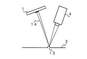
図1は、本発明による微小凹凸の検査方法を実行するための検査装置を示す構成図である。図に示すように、面状の拡散光源である主光源1からガラス等の被検物2に照射された光は、被検物2の表面で正反射され、CCDエリアカメラ等の撮像素子4に入力する。また、補助光源3が、補助光源3による被検物2における正反射光が撮像素子4に入射しないように、すなわち被検物2に対して浅い角度で光が入射するような位置に設置される。この実施の形態では、補助光源3は、被検物2に対して撮像素子4と同じ側に、また、被検物2の法線に対して撮像素子4と同じ側に設置されている。
【0009】
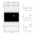
次に、演算装置5に取り込まれる画像について図2を参照して説明する。図2(A)において、(a)は主光源1からの光のみが被検物2に照射された場合の画像の例を示し、(b)は補助光源3からの光のみが被検物2に照射された場合の画像の例を示し、(c)は双方の光が被検物2に照射された場合の画像の例を示す模式図である。ここで、被検物2の表面に微小凹凸6とほこり7がある場合を考える。図2(B)の(a),(b),(c)は、それぞれ図2(A)の(a),(b),(c)に示された各画像におけるI−I断面の光量の例を示す説明図である。図2(B)には、微小凹凸6による信号61,62,63と、ほこり7による信号71,72,73が示されている。
【0010】
主光源1からの光のみが被検物2に照射された場合には、被検物2の全面での正反射光が撮像素子4に入射され明視野となる。微小凹凸6の部分では反射角が微妙にずれる。そのために、微小凹凸6の部分では、反射光が曲げられて暗点となる。ほこり7は散乱要素であるから、光が散乱される分だけ正反射光が減り、ほこり7の部分では暗点となる。よって、図2(B)の(a)に示すように、微小凹凸6およびほこり7の部分で光量が小さくなった信号が現れる。
【0011】
補助光源3からの光のみが被検物2に照射された場合には、正反射光が撮像素子4に入射されず暗視野になる。ほこり7の部分では光が散乱されて撮像素子4に入り、ほこり7の部分は明点となる。しかし、微小凹凸6の部分では、多少反射光が曲げられるものの、反射光は撮像素子4に入射されず明点とはならない。よって、図2(B)の(b)に示すように、ほこり7の部分で光量が大きくなった信号が現れる。
【0012】
主光源1からの光と補助光源3からの光が被検物2に同時に照射された場合には、主光源1による正反射光が撮像素子4に入射されるので明視野となる。そして、微小凹凸6の部分では、反射光が曲げられて暗点となる。一方、ほこり7の部分では、主光源1からの光の散乱による光量の減少と補助光源3からの光の散乱による光量の増加とが同時に起こる。しかし、補助光源3からの光の散乱による光量の増加量が主光源1からの光の散乱による光量の減少量よりも大きくなるように、補助光源3による被検物2の面の照度を主光源1による被検物2の面の照度に対して強くしておけば、ほこり7の部分では明点となる。よって、図2(B)の(c)に示すように、ほこり7の部分で光量が大きくなり、微小凹凸6の部分で光量が小さくなった信号が現れる。
【0013】
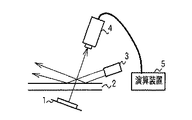
以上のことから、主光源1からの光と補助光源3からの光とを被検物2に同時に照射すれば、被検物2における微小凹凸6とほこり7とを区別して検出できることがわかる。具体的には、図1に示す主光源1と補助光源3とを点灯した状態で撮像素子4が被検物2の反射像を撮像し、画像を演算装置5に出力する。演算装置5は、入力した画像のうちの光量が小さい画素に対応した部分を微小凹凸6であると判定する。また、光量が大きい画素に対応した部分にほこり7が存在すると判定する。
【0014】
次に、図2(A)の(a)に示すような明視野で暗点にならないような微弱な微小凹凸も検出できるように感度を上げる方法について説明する。
図3(A)は、主光源1をストライプパターンとして、主光源1からの光と補助光源3からの光とを被検物2に同時に照射した場合の画像を示す模式図である。また、図3(B)は、図3(A)に示された各画像におけるI−I断面の光量の例を示す説明図である。図3(B)に示すように、ほこり7の部分で光量が大きくなった信号74が現れ、微小凹凸6の部分で光量が小さくなった信号64が現れる。また、黒ストライプの部分で光量が小さくなった信号8が現れる。
【0015】
ここで、撮像素子4の焦点は被検物2の表面(被検面)に合っているので、黒ストライプの部分ではエッジがぼけた小さな信号8が現れる。よって、画像に対してハイパスフィルタ処理を施すことによって、それらの信号8を除去することができる。
【0016】
上述したように、微小凹凸は、反射角が微妙にずれることによって、撮像された画像における光量が変わり、光量変化にもとづいて検出される。ストライプがない場合の明視野では主光源1の外の像が撮像されるほどに反射角度を変える凹凸の斜面が急な部分のみが検出される。すなわち、検出の感度は比較的低い。しかしストライプがある場合には、近傍の黒部分の反射像が撮像される程度の小さな反射角度の変化を引き起こす緩やかな傾斜の部分も検出される。すなわち、主光源1をストライプパターンにすると、検出の感度を上げることができる。また、ストライプパターンのピッチや白黒の比を変えることによって、どの程度の角度の凹凸まで検出するか調整することができる。すなわち、ストライプパターンのピッチや白黒の比を変えることによって、感度を変えることができる。
【0017】
次に、図4のフローチャートを参照して具体的な動作について説明する。
まず、図1に示す主光源1と補助光源3とを点灯した状態で撮像素子4が被検物2の反射像を撮像し画像を演算装置5に出力する。演算装置5は画像を取り込む(ステップS1)。そして、演算装置5は、スムージング等のローパスフィルタ処理を施す(ステップS21)。この結果、黒ストライプの像を含み、微小凹凸6とほこり7による信号が除去された画像が得られる。次いで、入力した原画像とローパスフィルタ処理が施された画像との差を算出する(ステップS22)。この結果、黒ストライプの部分が除去され、微小凹凸6とほこり7による信号が現れた画像が得られる。なお、ステップS21とステップS22の処理が、ハイパスフィルタ処理(ステップS2)となっている。
【0018】
演算装置5は、ステップS2で得られた画像を構成する各画素を、正のしきい値および負のしきい値と比較する。ここで、0は明視野の光量に相当する値である。図2(B)の(c)に示されたように、微小凹凸6の部分では光量が負の値として現れ、ほこり7は正の値として現れる。よって、正負のしきい値を適切に設定すれば、正のしきい値を越えた画素に相当する部分をほこり7、負のしきい値よりも小さい画素に相当する部分を微小凹凸6と判定することができる。
【0019】
以上のように、主光源1をストライプパターンとし、主光源1と補助光源3とを同時に点灯し、得られた画像についてハイパスフィルタ処理を施すことによって、微小凹凸6およびほこり7を、あるしきい値以下、以上として検出できる。そして、主光源1をストライプパターンにした場合には検出感度が上がっている。
なお、微小凹凸6が黒ストライプ上に存在する場合でも、それを問題なく検出することができる。図5〜図7は、そのことを説明するための説明図である。
【0020】
図5は、被検面に凹凸がない場合を示している。撮像素子4の焦点は被検面上にあるので、主光源1の面はぼけた状態になっている。つまり、撮像素子4の1画素が見る領域は光路10のように広がり、その画素には、黒ストライプ9より広い領域の平均的光量が入力される。図6は、被検面に微小凹部11がある場合を示している。微小凹部11は、焦点を結んだ直後に凹面鏡を入れた状態と同じ効果を示すので、主光源1の面において焦点ずれの影響を弱める。従って、撮像素子4の1画素が見る領域は光路12のように狭まり、撮像された画像において、その画素の信号は、図5に示された場合に比べて小さくなる。
【0021】
図7は、被検面に微小凸部13がある場合を示している。微小凸部13は焦点を結ぶ前に凸面鏡を入れた状態と同じ効果を示すので、焦点を結ぶ位置が遠くなって、やはり主光源1の面において焦点ずれの影響を弱める。従って、撮像素子4の1画素が見る領域は、やはり光路14のように狭まり、撮像された画像において、その画素の信号は、図5に示された場合に比べて小さくなる。
以上のように、黒ストライプの照射位置に微小凹凸があっても、微小凹凸がない場合に比べて画像における信号レベルが小さくなるので、微小凹凸は問題なく検出される。
【0022】
以上、被検物2の表面の微小凹凸をほこり等の散乱性欠点と区別して検出する場合について説明した。しかし、ほこり等の影響を除去して被検物2の表面の微小凹凸欠点を検出するのに本発明を適用できるだけでなく、ほこりのない状況では、主光源1と補助光源3とを同時に用いて、微小凹凸欠点を暗点、きずなどの散乱性欠点を明点として、それらを同時に区別して検出するために本発明を適用することもできる。
また、本発明によれば、微小凹凸の位置と大きさとを検出できるので、表面に凹凸が施された被検物2の凹凸むらを、ほこり等の影響をうけずに評価することもできる。さらに、被検物2の凹凸むらの評価と、きずなどの欠点の検出とを同時に行うこともできる。
【0023】
上記の実施の形態では、図1に示されたように、補助光源3が、被検物2に対して撮像素子4と同じ側に、また、被検物2の法線に対して撮像素子4と同じ側に設置されていた。しかし、図1に示された場合と同様に照射の光軸が被検面に近い角度に設定されていれば、図8に示すように、補助光源3が被検物2の法線に対して撮像素子4と反対側に設置されていても、上記の実施の形態の場合と同様の効果を得ることができる。さらに、図9に示すように、被検物2に対して撮像素子4とは反対側であって、補助光源3による被検物2の透過光が撮像素子4に入らないような位置に補助光源3を設置してもよい。この場合には、補助光源3による被検物2の透過光による散乱が微小凹凸と散乱性欠点とを識別する作用を果たす。
【0024】
また、図10および図11に示すように、被検物2に対して主光源1を撮像素子4と反対側に設置し、被検物2の透過光による明視野を形成するようにしても、上記の実施の形態の場合と同様の効果を得ることができる。その場合、図10に示すように、補助光源3を被検物2に対して撮像素子4と同じ側に設置してもよいし、図11に示すように、補助光源3を被検物2に対して撮像素子4と反対側に設置してもよい。なお、被検物2の透過光による明視野を形成する場合には、微小凹凸において透過光が微妙に屈折するために、撮像された画像において微小凹凸に部分が暗点になる。
【0025】
検査装置を、主光源1、補助光源3および撮像素子4がひとまとまりになった構成にすることもできる。そして、主光源1、補助光源3および撮像素子3と被検面との角度を一定に保ちつつ被検物2の形状に沿って検査装置を移動させることによって、撮像素子4の視野を越える広い範囲の検査を容易に行うことができる。
【0026】
以下、本発明の具体的適用例を説明する。
ブラウン管用ガラスの外面の微小な凹み群を検査対象とし、図1に示された反射光学系を用い、被検面の法線と撮像素子4の光軸とを15°傾けた。そして、ガラス面上で1画素が0.033mm×0.033mmとなるように、また、F16となる光学条件を設定した。主光源1として高周波の拡散光源にストライプフィルムを重ねたものを用い、ストライプパターンを、白と黒の幅が2:1の比でピッチ1.9mmとし、画像上で1ピッチが37画素に相当するように設定した。補助光源3としてファイバ光源を用い、被検面に対して25°の角度で光が照射されるようにファイバ光源を設置した。
【0027】
また、得られた画像に対して3×3のスムージング処理を2回行ってローパスフィルタ処理を行い、得られた原画像とローパスフィルタ処理が施された画像との差の画像において、しきい値以下の領域を欠点とした。
【0028】
そして、約10mm角の領域に対して被検面上の微小凹みの数を数える検査を用いたところ、目視で詳細に確認した数に対して検出率は86%であり、微小凹凸以外を検出した誤検出率は総検出数に対して9%であった。
【0029】
【発明の効果】
以上のように、本発明によれば、微小凹凸の検査方法を、主光源からの光を被検物に照射するとともに、出射される光の被検物表面のほこりの部分における散乱による光量の増加量が主光源からの光の被検物表面のほこりの部分における散乱による光量の減少量よりも大きくなるように、主光源の光度に対して光度が設定され、被検物における正反射光または透過光が受光部に入射しないよう設置された補助光源からの光を被検物に照射し、受光して得られた画像中の暗点を微小凹凸と判定し、画像中の明点をほこりと判定するように構成したので、ほこり等の散乱要因を選択的に光らせることができ、その結果、被検物表面の微小凹凸欠点を、ほこり等の他の欠点や誤検出要因と区別して検査することができ、精度のよい確実な検査を行うことができる。
【0030】
また、微小凹凸の検査装置を、出射される光の被検物表面のほこりの部分における散乱による光量の増加量が主光源からの光の被検物表面のほこりの部分における散乱による光量の減少量よりも大きくなるように、主光源の光度に対して光度が設定され、被検物における正反射光または透過光が受光部に入射しないよう設置された補助光源を備え、演算装置が、主光源からの光と補助光源からの光が同時に被検物に照射されている状態で受光して得られた画像中の各画素の信号レベルを判定し、画像中の暗点を微小凹凸と判定し、画像中の明点をほこりと判定する構成にしたので、ほこり等の散乱要因を選択的に光らせた画像を解析することによって微小凹凸を散乱要因と区別して検査することができるようになり、また、複数センサや光源および受光部の位置合わせを行う必要はなく、検査装置の調整や保守が容易化される効果がある。
【図面の簡単な説明】
【図1】 本発明による微小凹凸の検査装置を示す構成図である。
【図2】 (A)は撮像される画像の例を示す模式図、(B)は、(A)に示された各画像におけるI−I断面の光量の例を示す説明図である。
【図3】 ストライプパターンの主光源からの光と補助光源からの光とを被検物に同時に照射した場合に得られる画像を示す模式図である。
【図4】 演算装置の信号処理の一例を示すフローチャートである。
【図5】 被検面に凹凸がない場合の光路を示す説明図である。
【図6】 被検面に微小凹部がある場合の光路を示す説明図である。
【図7】 被検面に微小凸部がある場合の光路を示す説明図である。
【図8】 本発明による微小凹凸の検査装置の他の実施の形態を示す構成図である。
【図9】 本発明による微小凹凸の検査装置のさらに他の実施の形態を示す構成図である。
【図10】 本発明による微小凹凸の検査装置のさらに他の実施の形態を示す構成図である。
【図11】 本発明による微小凹凸の検査装置のさらに他の実施の形態を示す構成図である。
【符号の説明】
1 主光源
2 被検物
3 補助光源
4 撮像素子
5 演算装置[0001]
BACKGROUND OF THE INVENTION
The present invention relates to a method for inspecting micro unevenness used for inspection and evaluation of defects such as micro unevenness on the surface of an object having specularity or transparency such as glass.
[0002]
[Prior art]
As a general method for inspecting defects such as minute irregularities on the surface of a product such as glass having a specularity, there is a method by an inspector's visual inspection, which requires the skill of the inspector and is overlooked. It is difficult to eliminate mistakes. Moreover, when the required quality becomes high, it becomes difficult to respond by visual inspection. Therefore, various automatic inspection apparatuses have been proposed.
[0003]
For example, Japanese Patent Application Laid-Open No. 63-293448 discloses a method for detecting a defect using a plurality of lights among transmitted light, transmitted scattered light, reflected light, and reflected scattered light from a test object. . Japanese Patent Application Laid-Open No. 1-107103 discloses a method for detecting a defect using regular reflection light and irregular reflection light from a test object. Furthermore, Japanese Patent Application Laid-Open No. 4-238207 and Japanese Patent Application Laid-Open No. 5-215697 disclose a method in which a plurality of sensors are provided and a defect is detected based on the output of each sensor. In JP-A-8-152416 and JP-A-9-49806, a light source or a light source and a light receiving unit are set at a predetermined angle with respect to the test object, and transmitted light or reflection from the test object. A method for detecting defects based on light is disclosed.
[0004]
[Problems to be solved by the invention]
However, in the method using a plurality of lights or the method using a plurality of sensors although using one kind of light, the alignment between the sensors becomes difficult as the detection target becomes smaller and the required resolution becomes higher. Similarly, even in a method in which it is necessary to set the light source or the light source and the light receiving unit at a predetermined angle with respect to the test object, it is difficult to align the light source and the light receiving unit. Accordingly, there are problems that malfunctions due to misalignment and a decrease in detection sensitivity are caused, and a great deal of labor is required for adjustment and maintenance of the inspection apparatus.
[0005]
Therefore, the present invention does not require the use of a plurality of sensors when detecting a defect of the test object, does not require alignment of the sensor or the like, and removes fine irregularities in the test object such as dust. It is an object of the present invention to provide an inspection method and an inspection apparatus for minute irregularities that can be inspected and evaluated separately from scattering defects.
[0006]
[Means for Solving the Problems]
The method for inspecting minute unevenness according to the present invention receives light reflected from a surface of a test object or transmitted light from the test object using light emitted from a light source, and uses the image obtained by receiving the test object. A method for inspecting microscopic irregularities on a surface, in which the amount of increase in the amount of light due to scattering of light from the auxiliary light source in the dusty part of the surface of the test object is the dust on the surface of the test object from the main light source. The brightness of the auxiliary light source is set with respect to the light intensity of the main light source so that it is larger than the amount of decrease in the amount of light due to scattering in the area of, and the test object is irradiated with light from the main light source and Light from an auxiliary light source installed so that reflected light or transmitted light does not enter the light-receiving part is irradiated on the test object, and the dark spots in the image obtained by receiving the light are determined as minute irregularities, and the light in the image The point is determined to be dust. Moreover, you may use the light source which has a stripe pattern as a main light source.
[0007]
The micro uneven inspection apparatus according to the present invention receives reflected light reflected from the surface of the test object or transmitted light transmitted through the test object, and uses an image obtained by receiving the light. This is a micro uneven inspection device for inspecting micro unevenness on the surface of the test object, and the amount of increase in the amount of light due to scattering of the emitted light in the dust portion of the test object surface is the surface of the test object of light from the main light source The light intensity is set with respect to the light intensity of the main light source so as to be larger than the amount of light reduction due to scattering in the dust part , and the specularly reflected light or transmitted light from the test object is not incident on the light receiving part. An auxiliary light source is provided, and the computing device determines the signal level of each pixel in the image obtained by receiving light in a state where the light from the main light source and the light from the auxiliary light source are simultaneously irradiated on the test object, The dark spots in the image are judged to be minute irregularities, and the bright spots in the image Configured to determine that dust and.
[0008]
DETAILED DESCRIPTION OF THE INVENTION
Hereinafter, embodiments of the present invention will be described with reference to the drawings.
FIG. 1 is a block diagram showing an inspection apparatus for executing the method for inspecting minute unevenness according to the present invention. As shown in the figure, the light emitted from the
[0009]
Next, an image captured by the
[0010]
When only the light from the
[0011]
When only the light from the
[0012]
When the light from the main
[0013]
From the above, it can be seen that if the
[0014]
Next, a method for increasing the sensitivity so as to detect a weak minute unevenness that does not become a dark spot in a bright field as shown in FIG.
FIG. 3A is a schematic diagram showing an image when the test
[0015]
Here, since the focus of the
[0016]
As described above, the minute unevenness is detected based on a change in the amount of light due to a change in the amount of light in the captured image due to a slight shift in the reflection angle. In the bright field when there is no stripe, only a portion with a steeply uneven slope that changes the reflection angle is detected such that an image outside the main
[0017]
Next, a specific operation will be described with reference to the flowchart of FIG.
First, with the main
[0018]
The
[0019]
As described above, the main
Even when the
[0020]
FIG. 5 shows a case where the test surface has no irregularities. Since the focus of the
[0021]
FIG. 7 shows a case where there are minute
As described above, even if there is a minute unevenness at the irradiation position of the black stripe, the signal level in the image is smaller than when there is no minute unevenness, so the minute unevenness can be detected without any problem.
[0022]
Heretofore, the case has been described in which minute irregularities on the surface of the
Further, according to the present invention, since the position and size of the minute unevenness can be detected, the unevenness of the
[0023]
In the above embodiment, as shown in FIG. 1, the auxiliary
[0024]
Further, as shown in FIGS. 10 and 11, the main
[0025]
The inspection apparatus may be configured such that the main
[0026]
Hereinafter, specific application examples of the present invention will be described.
A small dent group on the outer surface of the cathode ray tube glass was used as an inspection target, and the normal of the test surface and the optical axis of the
[0027]
In addition, a 3 × 3 smoothing process is performed twice on the obtained image to perform a low-pass filter process. In an image of a difference between the obtained original image and an image subjected to the low-pass filter process, The following areas were regarded as defects.
[0028]
Then, using an inspection that counts the number of minute dents on the surface to be measured for an area of about 10 mm square, the detection rate is 86% with respect to the number confirmed in detail visually, and other than minute irregularities are detected. The false detection rate was 9% with respect to the total number of detections.
[0029]
【The invention's effect】
As described above, according to the present invention, the method for inspecting minute unevenness irradiates the object with light from the main light source, and the amount of light caused by scattering of the emitted light at the dust portion of the object surface. The light intensity is set with respect to the light intensity of the main light source so that the increase amount is larger than the light amount decrease amount due to scattering of light from the main light source on the dust surface of the object surface , and the specularly reflected light on the test object Alternatively, the test object is irradiated with light from an auxiliary light source installed so that the transmitted light does not enter the light receiving unit, and the dark spot in the image obtained by receiving the light is determined as a minute unevenness, and the bright spot in the image is determined. Since it is configured to determine dust, it is possible to selectively scatter scattering factors such as dust. Can be inspected and perform accurate and reliable inspection Door can be.
[0030]
Further, a device for inspecting a micro irregularities, decrease in amount of light due to scattering at the dust portion of the test object surface of the light from the light quantity increase mainly light source due to scattering in the dust portion of the surface of the test object of the emitted light A light intensity is set with respect to the light intensity of the main light source so as to be larger than the amount, and an auxiliary light source is provided so that the specularly reflected light or transmitted light from the test object does not enter the light receiving unit. Determines the signal level of each pixel in the image obtained by receiving light from the light source and the light from the auxiliary light source at the same time, and determines the dark spot in the image as minute unevenness However, since the bright spot in the image is determined to be dust, it is possible to inspect minute irregularities separately from the scattering factor by analyzing the image that selectively scatters the scattering factor such as dust. Also, multiple sensors and light sources It is not necessary to align the spare light receiving portion, the effect to be facilitated adjustment and maintenance of the inspection apparatus.
[Brief description of the drawings]
FIG. 1 is a configuration diagram showing an inspection apparatus for minute irregularities according to the present invention.
2A is a schematic diagram illustrating an example of an image to be captured, and FIG. 2B is an explanatory diagram illustrating an example of a light amount of an II section in each image illustrated in FIG. 2A.
FIG. 3 is a schematic diagram showing an image obtained when a test object is simultaneously irradiated with light from a main light source in a stripe pattern and light from an auxiliary light source.
FIG. 4 is a flowchart illustrating an example of signal processing of the arithmetic device.
FIG. 5 is an explanatory diagram showing an optical path when there is no unevenness on a test surface.
FIG. 6 is an explanatory diagram showing an optical path when there is a minute recess on the surface to be examined.
FIG. 7 is an explanatory diagram showing an optical path when there is a minute convex portion on the surface to be examined.
FIG. 8 is a configuration diagram showing another embodiment of a micro uneven inspection apparatus according to the present invention.
FIG. 9 is a block diagram showing still another embodiment of a micro uneven inspection apparatus according to the present invention.
FIG. 10 is a block diagram showing still another embodiment of a micro uneven inspection apparatus according to the present invention.
FIG. 11 is a configuration diagram showing still another embodiment of a micro uneven inspection apparatus according to the present invention.
[Explanation of symbols]
DESCRIPTION OF
Claims (3)
補助光源からの光の前記被検物表面のほこりの部分における散乱による光量の増加量が主光源からの光の前記被検物表面のほこりの部分における散乱による光量の減少量よりも大きくなるように、前記主光源の光度に対して該補助光源の光度を設定し、
前記主光源からの光を前記被検物に照射するとともに、前記被検物における正反射光または透過光が受光部に入射しないよう設置された前記補助光源からの光を前記被検物に照射し、
受光して得られた画像中の暗点を微小凹凸と判定し、画像中の明点をほこりと判定する
ことを特徴とする微小凹凸の検査方法。Receives light reflected from the surface of the test object or light transmitted through the test object and inspects the micro unevenness of the test object surface using the image obtained by receiving the light. An inspection method,
The amount of increase in the amount of light due to scattering of light from the auxiliary light source in the dust portion on the surface of the test object is larger than the amount of decrease in the amount of light due to scattering of light from the main light source in the dust portion of the surface of the test object. And setting the luminous intensity of the auxiliary light source with respect to the luminous intensity of the main light source,
Irradiate the object with light from the main light source, and irradiate the object with light from the auxiliary light source installed so that specularly reflected light or transmitted light from the object does not enter the light receiving unit. And
A method for inspecting microscopic unevenness, characterized in that a dark spot in an image obtained by receiving light is determined as microscopic unevenness, and a bright point in the image is determined as dust.
請求項1記載の微小凹凸の検査方法。The method for inspecting minute unevenness according to claim 1, wherein a light source having a stripe pattern is used as a main light source.
主光源と、
出射される光の前記被検物表面のほこりの部分における散乱による光量の増加量が前記主光源からの光の前記被検物表面のほこりの部分における散乱による光量の減少量よりも大きくなるように、前記主光源の光度に対して光度が設定され、前記被検物における正反射光または透過光が受光部に入射しないよう設置された補助光源と、
前記主光源からの光と前記補助光源からの光が同時に前記被検物に照射されている状態で得られた画像中の各画素の信号レベルを判定し、画像中の暗点を微小凹凸と判定し、画像中の明点をほこりと判定する演算装置と
を備えたことを特徴とする微小凹凸の検査装置。The light irradiated from the light source receives the reflected light reflected by the surface of the test object or the transmitted light transmitted through the test object, and inspects the micro unevenness of the test object surface using the image obtained by receiving the light. An inspection device for micro unevenness,
A main light source;
As the increase in the amount of light due to scattering at the dust portion of the test object surface of the emitted light is larger than the amount of decrease of light intensity due to scattering in the dust portion of the surface of the test object light from the main light source In addition, an auxiliary light source that is set so that the light intensity is set with respect to the light intensity of the main light source and the specularly reflected light or transmitted light in the test object does not enter the light receiving unit,
The signal level of each pixel in the image obtained in a state where the light from the main light source and the light from the auxiliary light source are simultaneously irradiated on the test object is determined, and the dark spots in the image are defined as micro unevenness An inspection device for micro unevenness, comprising: an arithmetic unit that determines and determines a bright point in an image as dust.
Priority Applications (1)
| Application Number | Priority Date | Filing Date | Title |
|---|---|---|---|
| JP13264398A JP4158227B2 (en) | 1998-04-27 | 1998-04-27 | Inspection method and inspection apparatus for minute unevenness |
Applications Claiming Priority (1)
| Application Number | Priority Date | Filing Date | Title |
|---|---|---|---|
| JP13264398A JP4158227B2 (en) | 1998-04-27 | 1998-04-27 | Inspection method and inspection apparatus for minute unevenness |
Publications (2)
| Publication Number | Publication Date |
|---|---|
| JPH11311510A JPH11311510A (en) | 1999-11-09 |
| JP4158227B2 true JP4158227B2 (en) | 2008-10-01 |
Family
ID=15086129
Family Applications (1)
| Application Number | Title | Priority Date | Filing Date |
|---|---|---|---|
| JP13264398A Expired - Fee Related JP4158227B2 (en) | 1998-04-27 | 1998-04-27 | Inspection method and inspection apparatus for minute unevenness |
Country Status (1)
| Country | Link |
|---|---|
| JP (1) | JP4158227B2 (en) |
Families Citing this family (15)
| Publication number | Priority date | Publication date | Assignee | Title |
|---|---|---|---|---|
| DE10122313A1 (en) * | 2001-05-08 | 2002-11-21 | Wolfgang P Weinhold | Method and device for the contactless examination of an object, in particular with regard to its surface shape |
| JP4575202B2 (en) * | 2005-03-24 | 2010-11-04 | 日本板硝子株式会社 | Defect inspection method and defect inspection apparatus for transparent plate-like body |
| JP2007271510A (en) * | 2006-03-31 | 2007-10-18 | Tsubakimoto Chain Co | Visual inspection method and visual inspection device |
| US7567344B2 (en) * | 2006-05-12 | 2009-07-28 | Corning Incorporated | Apparatus and method for characterizing defects in a transparent substrate |
| JP4960161B2 (en) | 2006-10-11 | 2012-06-27 | 日東電工株式会社 | Inspection data processing apparatus and inspection data processing method |
| KR101249168B1 (en) | 2009-12-18 | 2013-03-29 | 주식회사 포스코 | The method and system to control quality in cold rolling system |
| JP5768224B2 (en) * | 2010-03-26 | 2015-08-26 | パナソニックIpマネジメント株式会社 | Defect detection apparatus and defect detection method |
| JP2014145656A (en) * | 2013-01-29 | 2014-08-14 | Nikka Kk | Method and device for visualizing fine particle adhesion state |
| JP6934645B2 (en) * | 2017-01-25 | 2021-09-15 | 国立研究開発法人産業技術総合研究所 | Image processing method |
| JP7110777B2 (en) * | 2017-07-20 | 2022-08-02 | 日立金属株式会社 | Metal thin plate inspection device and metal thin plate inspection method |
| JP7135297B2 (en) * | 2017-10-27 | 2022-09-13 | 株式会社ニコン | Inspection device, inspection system, and inspection method |
| CN110672621B (en) * | 2019-10-10 | 2021-03-05 | 清华大学 | Illumination brightness adjustment-based automobile coating surface defect image quality optimization method |
| CN111351795A (en) * | 2020-02-27 | 2020-06-30 | 杨孝兰 | Mirror surface object and transparent object detection method based on special structured light |
| CN111443040A (en) * | 2020-05-14 | 2020-07-24 | 成都德图福思科技有限公司 | Imaging system and method for laser coding etching mark on surface of light-reflecting and light-transmitting composite material |
| JP7390278B2 (en) * | 2020-12-16 | 2023-12-01 | 株式会社日立ハイテクソリューションズ | Appearance inspection method, appearance inspection device, processing method and device for structures |
-
1998
- 1998-04-27 JP JP13264398A patent/JP4158227B2/en not_active Expired - Fee Related
Also Published As
| Publication number | Publication date |
|---|---|
| JPH11311510A (en) | 1999-11-09 |
Similar Documents
| Publication | Publication Date | Title |
|---|---|---|
| JP4511978B2 (en) | Surface flaw inspection device | |
| JP4158227B2 (en) | Inspection method and inspection apparatus for minute unevenness | |
| TWI408360B (en) | Apparatus for detecting particles on a glass surface and a method thereof | |
| US7105848B2 (en) | Dual level out-of-focus light source for amplification of defects on a surface | |
| JP4147682B2 (en) | Defect inspection method and inspection apparatus for test object | |
| EP0930498A2 (en) | Inspection apparatus and method for detecting defects | |
| JP2012078144A (en) | Surface defect inspection device for transparent body sheet-like material | |
| JP2007218889A (en) | Surface defect detection method and surface defect detecting device | |
| JP3021266B2 (en) | Optical steel sheet surface inspection equipment | |
| JPH06294749A (en) | Flaw inspection method for plat glass | |
| JPH10148619A (en) | Method and device for inspecting face defect of substrate under inspection | |
| JP2006138830A (en) | Surface defect inspection device | |
| KR20180136421A (en) | System and method for defect detection | |
| JPH11316195A (en) | Surface defect detecting device of transparent plate | |
| JP2006017685A (en) | Surface defect inspection device | |
| JP2001124538A (en) | Method and device for detecting defect in surface of object | |
| JP3078784B2 (en) | Defect inspection equipment | |
| JPH11248643A (en) | Detection device for foreign matter in transparent film | |
| JPH08178855A (en) | Method for inspecting light-transmissive object or specular object | |
| JP3222727B2 (en) | Optical member inspection device | |
| JPH09113465A (en) | Detection apparatus for surface fault for galvanized steel plate | |
| JPH0711414B2 (en) | Glass bottle uneven thickness inspection method | |
| JPH0311403B2 (en) | ||
| JP2002005845A (en) | Defect inspecting apparatus | |
| JP3293257B2 (en) | Surface defect inspection equipment |
Legal Events
| Date | Code | Title | Description |
|---|---|---|---|
| A521 | Written amendment |
Free format text: JAPANESE INTERMEDIATE CODE: A523 Effective date: 20050411 |
|
| A621 | Written request for application examination |
Free format text: JAPANESE INTERMEDIATE CODE: A621 Effective date: 20050411 |
|
| A977 | Report on retrieval |
Free format text: JAPANESE INTERMEDIATE CODE: A971007 Effective date: 20060922 |
|
| A131 | Notification of reasons for refusal |
Free format text: JAPANESE INTERMEDIATE CODE: A131 Effective date: 20070320 |
|
| A521 | Written amendment |
Free format text: JAPANESE INTERMEDIATE CODE: A523 Effective date: 20070507 |
|
| A131 | Notification of reasons for refusal |
Free format text: JAPANESE INTERMEDIATE CODE: A131 Effective date: 20071113 |
|
| A521 | Written amendment |
Free format text: JAPANESE INTERMEDIATE CODE: A523 Effective date: 20080115 |
|
| A131 | Notification of reasons for refusal |
Free format text: JAPANESE INTERMEDIATE CODE: A131 Effective date: 20080219 |
|
| A521 | Written amendment |
Free format text: JAPANESE INTERMEDIATE CODE: A523 Effective date: 20080306 |
|
| TRDD | Decision of grant or rejection written | ||
| A01 | Written decision to grant a patent or to grant a registration (utility model) |
Free format text: JAPANESE INTERMEDIATE CODE: A01 Effective date: 20080624 |
|
| A01 | Written decision to grant a patent or to grant a registration (utility model) |
Free format text: JAPANESE INTERMEDIATE CODE: A01 |
|
| A61 | First payment of annual fees (during grant procedure) |
Free format text: JAPANESE INTERMEDIATE CODE: A61 Effective date: 20080707 |
|
| FPAY | Renewal fee payment (event date is renewal date of database) |
Free format text: PAYMENT UNTIL: 20110725 Year of fee payment: 3 |
|
| FPAY | Renewal fee payment (event date is renewal date of database) |
Free format text: PAYMENT UNTIL: 20110725 Year of fee payment: 3 |
|
| FPAY | Renewal fee payment (event date is renewal date of database) |
Free format text: PAYMENT UNTIL: 20120725 Year of fee payment: 4 |
|
| FPAY | Renewal fee payment (event date is renewal date of database) |
Free format text: PAYMENT UNTIL: 20120725 Year of fee payment: 4 |
|
| S531 | Written request for registration of change of domicile |
Free format text: JAPANESE INTERMEDIATE CODE: R313531 |
|
| FPAY | Renewal fee payment (event date is renewal date of database) |
Free format text: PAYMENT UNTIL: 20120725 Year of fee payment: 4 |
|
| R371 | Transfer withdrawn |
Free format text: JAPANESE INTERMEDIATE CODE: R371 |
|
| S531 | Written request for registration of change of domicile |
Free format text: JAPANESE INTERMEDIATE CODE: R313531 |
|
| FPAY | Renewal fee payment (event date is renewal date of database) |
Free format text: PAYMENT UNTIL: 20120725 Year of fee payment: 4 |
|
| R350 | Written notification of registration of transfer |
Free format text: JAPANESE INTERMEDIATE CODE: R350 |
|
| FPAY | Renewal fee payment (event date is renewal date of database) |
Free format text: PAYMENT UNTIL: 20130725 Year of fee payment: 5 |
|
| LAPS | Cancellation because of no payment of annual fees |