JP4156946B2 - Acceleration sensor - Google Patents
Acceleration sensor Download PDFInfo
- Publication number
- JP4156946B2 JP4156946B2 JP2003048444A JP2003048444A JP4156946B2 JP 4156946 B2 JP4156946 B2 JP 4156946B2 JP 2003048444 A JP2003048444 A JP 2003048444A JP 2003048444 A JP2003048444 A JP 2003048444A JP 4156946 B2 JP4156946 B2 JP 4156946B2
- Authority
- JP
- Japan
- Prior art keywords
- cap
- semiconductor chip
- acceleration sensor
- chip substrate
- acceleration
- Prior art date
- Legal status (The legal status is an assumption and is not a legal conclusion. Google has not performed a legal analysis and makes no representation as to the accuracy of the status listed.)
- Expired - Fee Related
Links
Images


Classifications
-
- B—PERFORMING OPERATIONS; TRANSPORTING
- B81—MICROSTRUCTURAL TECHNOLOGY
- B81B—MICROSTRUCTURAL DEVICES OR SYSTEMS, e.g. MICROMECHANICAL DEVICES
- B81B7/00—Microstructural systems; Auxiliary parts of microstructural devices or systems
- B81B7/0032—Packages or encapsulation
- B81B7/0045—Packages or encapsulation for reducing stress inside of the package structure
- B81B7/0051—Packages or encapsulation for reducing stress inside of the package structure between the package lid and the substrate
-
- G—PHYSICS
- G01—MEASURING; TESTING
- G01P—MEASURING LINEAR OR ANGULAR SPEED, ACCELERATION, DECELERATION, OR SHOCK; INDICATING PRESENCE, ABSENCE, OR DIRECTION, OF MOVEMENT
- G01P1/00—Details of instruments
- G01P1/02—Housings
- G01P1/023—Housings for acceleration measuring devices
-
- G—PHYSICS
- G01—MEASURING; TESTING
- G01P—MEASURING LINEAR OR ANGULAR SPEED, ACCELERATION, DECELERATION, OR SHOCK; INDICATING PRESENCE, ABSENCE, OR DIRECTION, OF MOVEMENT
- G01P15/00—Measuring acceleration; Measuring deceleration; Measuring shock, i.e. sudden change of acceleration
- G01P15/02—Measuring acceleration; Measuring deceleration; Measuring shock, i.e. sudden change of acceleration by making use of inertia forces using solid seismic masses
- G01P15/08—Measuring acceleration; Measuring deceleration; Measuring shock, i.e. sudden change of acceleration by making use of inertia forces using solid seismic masses with conversion into electric or magnetic values
- G01P15/0802—Details
-
- G—PHYSICS
- G01—MEASURING; TESTING
- G01P—MEASURING LINEAR OR ANGULAR SPEED, ACCELERATION, DECELERATION, OR SHOCK; INDICATING PRESENCE, ABSENCE, OR DIRECTION, OF MOVEMENT
- G01P15/00—Measuring acceleration; Measuring deceleration; Measuring shock, i.e. sudden change of acceleration
- G01P15/02—Measuring acceleration; Measuring deceleration; Measuring shock, i.e. sudden change of acceleration by making use of inertia forces using solid seismic masses
- G01P15/08—Measuring acceleration; Measuring deceleration; Measuring shock, i.e. sudden change of acceleration by making use of inertia forces using solid seismic masses with conversion into electric or magnetic values
- G01P15/125—Measuring acceleration; Measuring deceleration; Measuring shock, i.e. sudden change of acceleration by making use of inertia forces using solid seismic masses with conversion into electric or magnetic values by capacitive pick-up
-
- H—ELECTRICITY
- H01—ELECTRIC ELEMENTS
- H01L—SEMICONDUCTOR DEVICES NOT COVERED BY CLASS H10
- H01L2224/00—Indexing scheme for arrangements for connecting or disconnecting semiconductor or solid-state bodies and methods related thereto as covered by H01L24/00
- H01L2224/01—Means for bonding being attached to, or being formed on, the surface to be connected, e.g. chip-to-package, die-attach, "first-level" interconnects; Manufacturing methods related thereto
- H01L2224/02—Bonding areas; Manufacturing methods related thereto
- H01L2224/04—Structure, shape, material or disposition of the bonding areas prior to the connecting process
- H01L2224/05—Structure, shape, material or disposition of the bonding areas prior to the connecting process of an individual bonding area
- H01L2224/0554—External layer
- H01L2224/0555—Shape
- H01L2224/05552—Shape in top view
- H01L2224/05554—Shape in top view being square
-
- H—ELECTRICITY
- H01—ELECTRIC ELEMENTS
- H01L—SEMICONDUCTOR DEVICES NOT COVERED BY CLASS H10
- H01L2224/00—Indexing scheme for arrangements for connecting or disconnecting semiconductor or solid-state bodies and methods related thereto as covered by H01L24/00
- H01L2224/01—Means for bonding being attached to, or being formed on, the surface to be connected, e.g. chip-to-package, die-attach, "first-level" interconnects; Manufacturing methods related thereto
- H01L2224/42—Wire connectors; Manufacturing methods related thereto
- H01L2224/47—Structure, shape, material or disposition of the wire connectors after the connecting process
- H01L2224/48—Structure, shape, material or disposition of the wire connectors after the connecting process of an individual wire connector
- H01L2224/4805—Shape
- H01L2224/4809—Loop shape
- H01L2224/48091—Arched
-
- H—ELECTRICITY
- H01—ELECTRIC ELEMENTS
- H01L—SEMICONDUCTOR DEVICES NOT COVERED BY CLASS H10
- H01L2224/00—Indexing scheme for arrangements for connecting or disconnecting semiconductor or solid-state bodies and methods related thereto as covered by H01L24/00
- H01L2224/01—Means for bonding being attached to, or being formed on, the surface to be connected, e.g. chip-to-package, die-attach, "first-level" interconnects; Manufacturing methods related thereto
- H01L2224/42—Wire connectors; Manufacturing methods related thereto
- H01L2224/47—Structure, shape, material or disposition of the wire connectors after the connecting process
- H01L2224/48—Structure, shape, material or disposition of the wire connectors after the connecting process of an individual wire connector
- H01L2224/481—Disposition
- H01L2224/48135—Connecting between different semiconductor or solid-state bodies, i.e. chip-to-chip
- H01L2224/48137—Connecting between different semiconductor or solid-state bodies, i.e. chip-to-chip the bodies being arranged next to each other, e.g. on a common substrate
-
- H—ELECTRICITY
- H01—ELECTRIC ELEMENTS
- H01L—SEMICONDUCTOR DEVICES NOT COVERED BY CLASS H10
- H01L2224/00—Indexing scheme for arrangements for connecting or disconnecting semiconductor or solid-state bodies and methods related thereto as covered by H01L24/00
- H01L2224/01—Means for bonding being attached to, or being formed on, the surface to be connected, e.g. chip-to-package, die-attach, "first-level" interconnects; Manufacturing methods related thereto
- H01L2224/42—Wire connectors; Manufacturing methods related thereto
- H01L2224/47—Structure, shape, material or disposition of the wire connectors after the connecting process
- H01L2224/48—Structure, shape, material or disposition of the wire connectors after the connecting process of an individual wire connector
- H01L2224/481—Disposition
- H01L2224/48151—Connecting between a semiconductor or solid-state body and an item not being a semiconductor or solid-state body, e.g. chip-to-substrate, chip-to-passive
- H01L2224/48221—Connecting between a semiconductor or solid-state body and an item not being a semiconductor or solid-state body, e.g. chip-to-substrate, chip-to-passive the body and the item being stacked
- H01L2224/48245—Connecting between a semiconductor or solid-state body and an item not being a semiconductor or solid-state body, e.g. chip-to-substrate, chip-to-passive the body and the item being stacked the item being metallic
- H01L2224/48247—Connecting between a semiconductor or solid-state body and an item not being a semiconductor or solid-state body, e.g. chip-to-substrate, chip-to-passive the body and the item being stacked the item being metallic connecting the wire to a bond pad of the item
-
- H—ELECTRICITY
- H01—ELECTRIC ELEMENTS
- H01L—SEMICONDUCTOR DEVICES NOT COVERED BY CLASS H10
- H01L2224/00—Indexing scheme for arrangements for connecting or disconnecting semiconductor or solid-state bodies and methods related thereto as covered by H01L24/00
- H01L2224/01—Means for bonding being attached to, or being formed on, the surface to be connected, e.g. chip-to-package, die-attach, "first-level" interconnects; Manufacturing methods related thereto
- H01L2224/42—Wire connectors; Manufacturing methods related thereto
- H01L2224/47—Structure, shape, material or disposition of the wire connectors after the connecting process
- H01L2224/49—Structure, shape, material or disposition of the wire connectors after the connecting process of a plurality of wire connectors
- H01L2224/491—Disposition
- H01L2224/4912—Layout
- H01L2224/49171—Fan-out arrangements
-
- H—ELECTRICITY
- H01—ELECTRIC ELEMENTS
- H01L—SEMICONDUCTOR DEVICES NOT COVERED BY CLASS H10
- H01L2224/00—Indexing scheme for arrangements for connecting or disconnecting semiconductor or solid-state bodies and methods related thereto as covered by H01L24/00
- H01L2224/01—Means for bonding being attached to, or being formed on, the surface to be connected, e.g. chip-to-package, die-attach, "first-level" interconnects; Manufacturing methods related thereto
- H01L2224/42—Wire connectors; Manufacturing methods related thereto
- H01L2224/47—Structure, shape, material or disposition of the wire connectors after the connecting process
- H01L2224/49—Structure, shape, material or disposition of the wire connectors after the connecting process of a plurality of wire connectors
- H01L2224/491—Disposition
- H01L2224/4912—Layout
- H01L2224/49175—Parallel arrangements
-
- H—ELECTRICITY
- H01—ELECTRIC ELEMENTS
- H01L—SEMICONDUCTOR DEVICES NOT COVERED BY CLASS H10
- H01L2924/00—Indexing scheme for arrangements or methods for connecting or disconnecting semiconductor or solid-state bodies as covered by H01L24/00
- H01L2924/15—Details of package parts other than the semiconductor or other solid state devices to be connected
- H01L2924/181—Encapsulation
-
- H—ELECTRICITY
- H01—ELECTRIC ELEMENTS
- H01L—SEMICONDUCTOR DEVICES NOT COVERED BY CLASS H10
- H01L2924/00—Indexing scheme for arrangements or methods for connecting or disconnecting semiconductor or solid-state bodies as covered by H01L24/00
- H01L2924/30—Technical effects
- H01L2924/301—Electrical effects
- H01L2924/3025—Electromagnetic shielding
Description
【0001】
【発明の属する技術分野】
この発明は、加速度センサに関し、例えば自動車のエアバッグシステムやその他の民生機器に採用可能である。
【0002】
【従来の技術】
現在、大半の自動車にエアバッグシステムが採用されている。一般にエアバッグシステムには、衝撃を検出するための加速度センサが組み込まれている。
【0003】
種々の自動車にこの加速度センサを組み込み可能とするために、加速度センサを小型化、低コスト化する努力が払われてきた。例えば、加速度センサの加速度検出部及び信号処理部を構成する半導体チップを覆うパッケージは、金属製のものから樹脂製のものへと切り替えられている。
【0004】
さて、加速度検出部の半導体チップの基板表面には、加速度検出用の可動部たる質量体が形成されている。この質量体の可動空間を確保し、可動空間内にゴミや水などを入り込ませないために、キャップが半導体チップ基板表面に接着される。これにより質量体の可動空間は密閉される。かかる技術は特許文献1に紹介されている。
【0005】
なお、その他にこの出願の発明に関連する先行技術文献情報としては、特許文献2ないし4がある。
【0006】
【特許文献1】
特開平8−114622号公報
【特許文献2】
特開平10−2911号公報
【特許文献3】
特開2001−185737号公報
【特許文献4】
特開2001−337105号公報
【0007】
【発明が解決しようとする課題】
上記のように加速度センサの半導体チップ基板表面にはキャップが設けられるが、このキャップには、樹脂パッケージのモールド時や使用中の環境温度の変化時に樹脂パッケージから応力がかかりやすい。
【0008】
キャップに応力がかかると、その応力の強度及び頻度にもよるが、クラックがキャップに生じることがある。そして、キャップにクラックが生じると、クラックを介して質量体の可動空間の密閉が破れやすい。
【0009】
可動空間の密閉が破れると、水分等が可動空間内に入り込んで質量体に付着しやすい。すると、質量体の変位特性が変動し、加速度の検出に影響を及ぼす可能性がある。
【0010】
クラックの発生を防止するには、キャップや半導体チップ基板を十分に厚く形成して、それらの剛性を高めるのが効果的である。しかし、このような対策では、加速度センサ小型化の要請に反するものとなってしまう。
【0011】
この発明は上記の事情に鑑みてなされたものであり、質量体の可動空間を密閉するキャップや半導体チップ基板を十分に厚く形成できない場合であっても、キャップにクラックが生じにくい構造の加速度センサを提供することにある。
【0012】
【課題を解決するための手段】
請求項1に記載の発明は、加速度を検出するための可動部を有する加速度検出部が形成された半導体チップ基板と、前記半導体チップ基板の表面に設けられ、前記可動部の可動空間を確保し、前記可動空間を密閉する天井と少なくとも1つの壁部とを含むキャップと、前記キャップにかかる応力を吸収する応力吸収部とを備え、前記キャップは前記キャップの前記少なくとも1つの壁部と前記半導体チップ基板との間に介在するキャップ土台部を含み、前記応力吸収部は、前記キャップ土台部の少なくとも1つの側面に対して、前記半導体チップ基板の前記表面に平行に設けられた少なくと一つの溝である加速度センサである。
【0016】
【発明の実施の形態】
<実施の形態1>
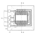
図1は、本実施の形態に係る加速度センサの全体構成を示す上面図である。図1に示すように、この加速度センサは、信号処理チップCP1、加速度検出部たる加速度検出チップCP2、リードLD及びダイパッドDPを含んでいる。
【0017】
信号処理チップCP1及び加速度検出チップCP2はともに、ダイパッドDP上に載置されている。加速度検出チップCP2のパッドPD1と信号処理チップCP1のパッドPD2とはワイヤWR1で接続され、信号処理チップCP1のパッドPD3とリードLDとはワイヤWR2で接続されている。そして、これらの構造は樹脂製パッケージPKで覆われている。
【0018】
なお、リードLDの一部は外部端子として樹脂製パッケージPKから露出する。また、図1では内部構造を示すために樹脂製パッケージPKを透明にし、隠れ線(破線)で示している。
【0019】
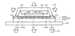
図2および図3は、加速度検出チップCP2の上面および断面をそれぞれ示す図である。なお、図3は図2内の切断線III−IIIにおける断面図である。図1ないし図3に示すように、加速度検出チップCP2の半導体チップ基板SBの表面には、単結晶シリコン等で形成した上述のキャップCAが接着されている。なお、図2では内部構造を示すためにキャップCAを透明にし、隠れ線(破線)で示している。
【0020】
加速度検出チップCP2においては、半導体チップ基板SBはシリコン基板SBaとその上面に形成されたシリコン酸化膜SBbとで構成されている。また、パッドPD1を構成するパッドPD1a〜PD1dが半導体チップ基板SBの表面内に形成されている。そして、パッドPD1a〜PD1dにそれぞれ接続された配線LNa〜LNdも半導体チップ基板SBの表面内に形成されている。また、配線LNcに接続されたシールド電極SEも半導体チップ基板SBの表面内に形成されている。
【0021】
また、半導体チップ基板SB上には、加速度を検出するための質量体MS、配線LNdに接続された固定電極FE1、配線LNaに接続された固定電極FE2、配線LNbに接続された質量体MSの支持部SPがそれぞれ形成されている。なお、質量体MSは梁部BMにより支持部SPに連結され、中空に保持されている。
【0022】
半導体チップ基板SBの表面やその上部の構造はいずれも、半導体製造技術を用いて形成される。すなわち、フォトリソグラフィ技術やエッチング技術、不純物イオン注入技術等を用いて、図1ないし図3に示された各部の構造は形成される。例えば、質量体MSや固定電極FE1,FE2、支持部SP、梁部BM等は、半導体チップ基板SB上にエピタキシャル成長させたシリコンをフォトリソグラフィ技術及びエッチング技術を用いてパターニングすることにより、図示した形状に形成される。
【0023】
質量体MSの両翼には、櫛状電極たる可動電極MEが設けられる。固定電極FE1,FE2は、この可動電極MEに面するよう配置されている。加速度が加わると梁部BMが撓んで質量体MSが変位し、可動電極MEと固定電極FE1,FE2との電極間距離が変動する。電極間距離が変動すれば、両電極間の静電容量も変化する。よって、両電極間の静電容量の変化を検出することにより、加速度の検出が行える。
【0024】
すなわち、質量体MSは加速度を検出するための可動部として機能し、固定電極FE1,FE2および質量体MSの可動電極MEが加速度検出部として機能する。
【0025】
キャップCAは、質量体MSの可動空間を確保し、可動空間を密閉するように半導体チップ基板SBの表面に接着されている。なお、図3に示すように厳密には、キャップCAはキャップ土台部FDを介して半導体チップ基板SBの表面に接着される。
【0026】
図3では、可動空間内において、半導体チップ基板SBの表面に対向するキャップCAの天井面と、天井面と半導体チップ基板SBの表面とをつなぐ壁面との境界部分CNに、上述のクラックCKを示している。キャップCAや半導体チップ基板SBに外部からストレスSTが加わると、天井支持部たる壁面の終端部でもある境界部分CNにこのようなクラックCKが発生しやすい。
【0027】
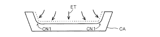
そこで、本実施の形態においては、図4に示すように可動空間内のキャップCAの天井面と壁面との境界部分CN1を曲面で構成する。このように、境界部分CN1を曲面で構成すれば、キャップCAに応力がかかったとしても、クラックの生じやすい境界部分CN1において応力は分散され、キャップCAでのクラック発生の可能性を低くすることができる。
【0028】
よって、キャップCAや半導体チップ基板SBを十分に厚く形成できない場合であっても、キャップCAにクラックが生じにくい構造の加速度センサを実現できる。
【0029】
なお、図4においてはキャップ土台部FDの詳細構成を示している。キャップ土台部FDは例えば、シリコン窒化膜FDa、ドープトポリシリコン膜FDb、シリコン酸化膜FDc、ノンドープトポリシリコン膜FDd、金属膜(例えばチタン膜またはニッケル膜)FDeを積層した積層膜で構成される。
【0030】
キャップCAの製造方法について以下に示す。まず、例えばシリコン基板に異方性エッチング(例えばKOHを用いたウェットエッチング)を行い、所定の結晶面を露出させて、可動空間内のキャップCAの天井面と壁面とを形成する。この段階では、天井面と壁面との境界部分は曲面となっていない。
【0031】
続いて、図5に示すようにキャップCAの天井面と壁面とに等方性エッチングET(例えば硝酸、酢酸、フッ酸をあわせ用いたウェットエッチング)を行う。これにより、キャップCAの天井面と壁面との境界部分CN1が曲面となる。
【0032】
<実施の形態2>
図6は、本実施の形態に係る加速度センサの加速度検出チップのうちキャップの接着部近傍を示した断面図である。
【0033】
本実施の形態においては、キャップCAと半導体チップ基板SBとの間に介在して両者を接着するキャップ土台部FDの側面に、溝GRが設けられる。より具体的には、キャップ土台部FDを構成する積層膜の一部たるドープトポリシリコン膜FDb1に溝GRが設けられる。なお、溝GRは例えば半導体チップ基板SBの表面と平行に設けられる。
【0034】
ドープトポリシリコン膜FDbがドープトポリシリコン膜FDb1に置換されていることと境界部分CNが曲面で構成されていないこと以外は、図4における構成と同じであるので、その他の部分の説明は省略する。
【0035】
このように、キャップ土台部FDの側面に溝GRが設けられておれば、半導体チップ基板SBが撓んだ場合であっても、溝GRが半導体チップ基板SBからの応力を吸収し、キャップCAでのクラック発生の可能性を低くすることができる。よって、キャップCAや半導体チップ基板SBを十分に厚く形成できない場合であっても、キャップCAにクラックが生じにくい構造の加速度センサを実現できる。
【0036】
図7ないし図10は、キャップ土台部FDの側面に溝GRを設ける製造方法を示す図である。
【0037】
まず、基板SBを構成するシリコン酸化膜SBb上に、CVD(Chemical Vapor Deposition)法等を用いてシリコン窒化膜およびドープトポリシリコン膜をこの順に積層して形成する。そして、フォトリソグラフィ技術およびエッチング技術を用いて、図7に示すようにシリコン窒化膜FDaおよびドープトポリシリコン膜FDb1aのパターニングを行う。
【0038】
次に、図8に示すように、シリコン窒化膜FDaおよびドープトポリシリコン膜FDb1aの膜厚に加えて溝GRの幅の分だけ厚くした膜厚のマスク膜(例えばシリコン酸化膜)MKを、シリコン酸化膜SBb上およびドープトポリシリコン膜FDb1a上に形成する。そして、シリコン窒化膜FDaおよびドープトポリシリコン膜FDb1aのパターニング幅よりも両側面の溝GRの深さの分だけ狭い開口幅の開口部OP1を、フォトリソグラフィ技術およびエッチング技術を用いてマスク膜MKに設ける。
【0039】
続いて、ドープトポリシリコン膜をマスク膜MK上およびドープトポリシリコン膜FDb1a上に形成する。そして、フォトリソグラフィ技術およびエッチング技術を用いて、図9に示すようにシリコン窒化膜FDaおよびドープトポリシリコン膜FDb1aのパターニング幅と同じパターニング幅でドープトポリシリコン膜FDb1bのパターニングを行う。
【0040】
その後、図10に示すようにマスク膜MKを除去すれば、溝GRが形成されたドープトポリシリコン膜FDb1が得られる。
【0041】
<実施の形態3>
図11は、本実施の形態に係る加速度センサの加速度検出チップ近傍を示した断面図である。
【0042】
本実施の形態においては、キャップCAよりも弾性率の低い(すなわち軟らかい)発泡性樹脂FRにキャップCAを覆わせる。発泡性樹脂FRには、例えばシリコーンゲルを採用すればよい。これにより、外部や図1に示した樹脂製パッケージPKから応力STがかかったとしても、発泡性樹脂FRが変形したり、あるいは発泡性樹脂FR内部の空隙がつぶれたりすることになり、応力STを吸収できる。
【0043】
なお、キャップ土台部FDに溝が設けられないこと以外は、図6における構成と同じであるので説明は省略する。
【0044】
本実施の形態に係る加速度センサによれば、キャップCAよりも弾性率の低い発泡性樹脂FRが樹脂パッケージ等からの応力STを吸収し、キャップCAでのクラック発生の可能性を低くすることができる。よって、キャップCAや半導体チップ基板SBを十分に厚く形成できない場合であっても、キャップCAにクラックが生じにくい構造の加速度センサを実現できる。
【0045】
<実施の形態4>
図12および図13は、本実施の形態に係る加速度センサの加速度検出チップCP2の上面および断面をそれぞれ示す図である。なお、図13は図12内の切断線XIII−XIIIにおける断面図である。図12および図13に示すように、加速度検出チップCP2の半導体チップ基板SBの表面には、キャップCA1が接着されている。なお、図12においても図2と同様、内部構造を示すためにキャップCA1を透明にし、隠れ線(破線)で示している。
【0046】
キャップCA1の構造は実施の形態1ないし3におけるキャップCAの構造とは異なり、可動空間内においてキャップCA1の天井面の一部に半導体チップ基板SBの表面に到達する支柱CA1aが設けられている。また、質量体MS1の構造も実施の形態1ないし3における質量体MSの構造とは異なり、その中央部に貫通孔OP2が設けられている。そして、支柱CA1aは、質量体MS1に触れることなく貫通孔OP2を貫通する。
【0047】
また、シールド電極SE1の構造も実施の形態1ないし3におけるシールド電極SEの構造とは異なり、貫通孔OP2の直下部には電極が形成されていない。これにより支柱CA1aがシールド電極SE1に接触することはない。
【0048】
なお、上記各点と発泡性樹脂FRが設けられないこと以外は、図11における構成と同じであるので、その他の部分の説明は省略する。
【0049】
本実施の形態に係る加速度センサにおいては、可動空間内においてキャップCA1の天井面の一部と半導体チップ基板SBの表面との間に支柱CA1aが設けられる。これにより、キャップCA1に応力がかかったとしても、キャップCA1の天井面が撓みにくく、キャップCA1でのクラック発生の可能性を低くすることができる。よって、キャップCA1や半導体チップ基板SBを十分に厚く形成できない場合であっても、キャップCA1にクラックが生じにくい構造の加速度センサを実現できる。
【0050】
また、本実施の形態に係る加速度センサにおいては、キャップCA1の支柱CA1aは質量体MS1に触れることなく質量体MS1の貫通孔OP2を貫通する。これにより、質量体MS1の加速度による変位を妨げることなく、支柱CA1aを可動空間内の質量体MS1の位置する場所に重ねて設けることができる。よって、可動空間を広げることなく、支柱CA1aを設けることができ、加速度センサの小型化に資する。
【0051】
<その他>
上記の各実施の形態の各構造については、それぞれを単独で加速度センサに採用しても良いし、また、複数を組み合わせて採用しても良い。
【0052】
【発明の効果】
請求項1に記載の発明によれば、キャップ土台部の側面には、溝が設けられている。よって、半導体チップ基板が撓んだ場合であっても、キャップ土台部の溝が半導体チップ基板からの応力を吸収し、キャップでのクラック発生の可能性を低くすることができる。よって、キャップや半導体チップ基板を十分に厚く形成できない場合であっても、キャップにクラックが生じにくい構造の加速度センサを実現できる。
【図面の簡単な説明】
【図1】 実施の形態1に係る加速度センサの全体構成を示す上面図である。
【図2】 実施の形態1に係る加速度センサのうち加速度検出チップの上面図である。
【図3】 実施の形態1に係る加速度センサのうち加速度検出チップの断面図である。
【図4】 実施の形態1に係る加速度センサの加速度検出チップのうちキャップの接着部近傍を示した断面図である。
【図5】 実施の形態1に係る加速度センサの加速度検出チップのうちキャップの製造方法を示した図である。
【図6】 実施の形態2に係る加速度センサの加速度検出チップのうちキャップの接着部近傍を示した断面図である。
【図7】 実施の形態2に係る加速度センサの加速度検出チップのうちキャップ土台部の製造方法を示した断面図である。
【図8】 実施の形態2に係る加速度センサの加速度検出チップのうちキャップ土台部の製造方法を示した断面図である。
【図9】 実施の形態2に係る加速度センサの加速度検出チップのうちキャップ土台部の製造方法を示した断面図である。
【図10】 実施の形態2に係る加速度センサの加速度検出チップのうちキャップ土台部の製造方法を示した断面図である。
【図11】 実施の形態3に係る加速度センサの加速度検出チップ近傍を示した断面図である。
【図12】 実施の形態4に係る加速度センサのうち加速度検出チップの上面図である。
【図13】 実施の形態4に係る加速度センサのうち加速度検出チップの断面図である。
【符号の説明】
SB 半導体チップ基板、CA,CA1 キャップ、FD キャップ土台部、FR 発泡性樹脂、CA1a 支柱、OP2 貫通孔。[0001]
BACKGROUND OF THE INVENTION
The present invention relates to an acceleration sensor, and can be applied to, for example, an automobile airbag system and other consumer devices.
[0002]
[Prior art]
Currently, airbag systems are used in most automobiles. In general, an airbag system incorporates an acceleration sensor for detecting an impact.
[0003]
In order to be able to incorporate this acceleration sensor in various automobiles, efforts have been made to reduce the size and cost of the acceleration sensor. For example, a package that covers a semiconductor chip constituting an acceleration detection unit and a signal processing unit of an acceleration sensor is switched from a metal one to a resin one.
[0004]
A mass body that is a movable part for acceleration detection is formed on the substrate surface of the semiconductor chip of the acceleration detection part. A cap is bonded to the surface of the semiconductor chip substrate in order to secure a movable space of the mass body and prevent dust and water from entering the movable space. Thereby, the movable space of the mass body is sealed. Such a technique is introduced in
[0005]
In addition, there are Patent Documents 2 to 4 as prior art document information related to the invention of this application.
[0006]
[Patent Document 1]
JP-A-8-114622 [Patent Document 2]
Japanese Patent Laid-Open No. 10-2911 [Patent Document 3]
JP 2001-185737 A [Patent Document 4]
Japanese Patent Laid-Open No. 2001-337105
[Problems to be solved by the invention]
As described above, a cap is provided on the surface of the semiconductor chip substrate of the acceleration sensor, and stress is easily applied to the cap from the resin package when the resin package is molded or when the environmental temperature changes during use.
[0008]
When stress is applied to the cap, cracks may occur in the cap depending on the strength and frequency of the stress. And when a crack arises in a cap, sealing of the movable space of a mass body is easy to be broken through a crack.
[0009]
When the sealing of the movable space is broken, moisture or the like easily enters the movable space and adheres to the mass body. Then, the displacement characteristics of the mass body may fluctuate, which may affect the detection of acceleration.
[0010]
In order to prevent the occurrence of cracks, it is effective to increase the rigidity of the cap and the semiconductor chip substrate by forming them sufficiently thick. However, such a measure is contrary to the demand for downsizing the acceleration sensor.
[0011]
The present invention has been made in view of the above circumstances, and even when a cap or a semiconductor chip substrate that seals the movable space of a mass body cannot be formed sufficiently thick, an acceleration sensor having a structure in which cracks do not easily occur in the cap. Is to provide.
[0012]
[Means for Solving the Problems]
The invention according to
[0016]
DETAILED DESCRIPTION OF THE INVENTION
<
FIG. 1 is a top view showing the overall configuration of the acceleration sensor according to the present embodiment. As shown in FIG. 1, the acceleration sensor includes a signal processing chip CP1, an acceleration detection chip CP2 serving as an acceleration detection unit, a lead LD, and a die pad DP.
[0017]
Both the signal processing chip CP1 and the acceleration detection chip CP2 are placed on the die pad DP. The pad PD1 of the acceleration detection chip CP2 and the pad PD2 of the signal processing chip CP1 are connected by a wire WR1, and the pad PD3 of the signal processing chip CP1 and the lead LD are connected by a wire WR2. These structures are covered with a resin package PK.
[0018]
A part of the lead LD is exposed from the resin package PK as an external terminal. Further, in FIG. 1, the resin package PK is made transparent to show the internal structure, and is shown by hidden lines (broken lines).
[0019]
2 and 3 are views showing the upper surface and the cross section of the acceleration detection chip CP2, respectively. 3 is a cross-sectional view taken along a cutting line III-III in FIG. As shown in FIGS. 1 to 3, the above-described cap CA formed of single crystal silicon or the like is bonded to the surface of the semiconductor chip substrate SB of the acceleration detection chip CP2. In FIG. 2, the cap CA is made transparent to show the internal structure, and is shown by a hidden line (broken line).
[0020]
In the acceleration detection chip CP2, the semiconductor chip substrate SB is composed of a silicon substrate SBa and a silicon oxide film SBb formed on the upper surface thereof. Further, pads PD1a to PD1d constituting the pad PD1 are formed in the surface of the semiconductor chip substrate SB. Then, wirings LNa to LNd connected to the pads PD1a to PD1d are also formed in the surface of the semiconductor chip substrate SB. A shield electrode SE connected to the wiring LNc is also formed in the surface of the semiconductor chip substrate SB.
[0021]
Further, on the semiconductor chip substrate SB, there are a mass body MS for detecting acceleration, a fixed electrode FE1 connected to the wiring LNd, a fixed electrode FE2 connected to the wiring LNa, and a mass body MS connected to the wiring LNb. Support portions SP are respectively formed. The mass body MS is connected to the support portion SP by the beam portion BM and is held hollow.
[0022]
The surface of the semiconductor chip substrate SB and the structure of the upper part thereof are both formed using semiconductor manufacturing technology. That is, the structure of each part shown in FIGS. 1 to 3 is formed by using a photolithography technique, an etching technique, an impurity ion implantation technique, or the like. For example, the mass body MS, the fixed electrodes FE1, FE2, the support portion SP, the beam portion BM, and the like are formed by patterning silicon epitaxially grown on the semiconductor chip substrate SB using a photolithography technique and an etching technique. Formed.
[0023]
A movable electrode ME as a comb-like electrode is provided on both wings of the mass body MS. The fixed electrodes FE1, FE2 are arranged so as to face the movable electrode ME. When acceleration is applied, the beam portion BM is bent and the mass body MS is displaced, and the distance between the movable electrode ME and the fixed electrodes FE1, FE2 varies. If the distance between the electrodes varies, the capacitance between the two electrodes also changes. Therefore, acceleration can be detected by detecting a change in capacitance between both electrodes.
[0024]
That is, the mass body MS functions as a movable portion for detecting acceleration, and the fixed electrodes FE1, FE2 and the movable electrode ME of the mass body MS function as an acceleration detection portion.
[0025]
The cap CA secures the movable space of the mass body MS and is bonded to the surface of the semiconductor chip substrate SB so as to seal the movable space. Strictly speaking, as shown in FIG. 3, the cap CA is bonded to the surface of the semiconductor chip substrate SB via the cap base portion FD.
[0026]
In FIG. 3, in the movable space, the above-mentioned crack CK is applied to the boundary portion CN between the ceiling surface of the cap CA facing the surface of the semiconductor chip substrate SB and the wall surface connecting the ceiling surface and the surface of the semiconductor chip substrate SB. Show. When the stress ST is applied to the cap CA and the semiconductor chip substrate SB from the outside, such a crack CK is likely to occur in the boundary portion CN that is also the terminal portion of the wall surface serving as the ceiling support portion.
[0027]
Therefore, in the present embodiment, as shown in FIG. 4, the boundary portion CN1 between the ceiling surface and the wall surface of the cap CA in the movable space is formed of a curved surface. Thus, if the boundary portion CN1 is formed of a curved surface, even if stress is applied to the cap CA, the stress is dispersed in the boundary portion CN1 where cracks are likely to occur, and the possibility of occurrence of cracks in the cap CA is reduced. Can do.
[0028]
Therefore, even when the cap CA and the semiconductor chip substrate SB cannot be formed sufficiently thick, it is possible to realize an acceleration sensor having a structure in which cracks are unlikely to occur in the cap CA.
[0029]
FIG. 4 shows a detailed configuration of the cap base portion FD. The cap base FD is composed of a laminated film in which, for example, a silicon nitride film FDa, a doped polysilicon film FDb, a silicon oxide film FDc, a non-doped polysilicon film FDd, and a metal film (for example, a titanium film or a nickel film) FDe are laminated. The
[0030]
The manufacturing method of the cap CA is shown below. First, for example, anisotropic etching (for example, wet etching using KOH) is performed on a silicon substrate to expose a predetermined crystal surface, thereby forming a ceiling surface and a wall surface of the cap CA in the movable space. At this stage, the boundary portion between the ceiling surface and the wall surface is not curved.
[0031]
Subsequently, as shown in FIG. 5, isotropic etching ET (for example, wet etching using nitric acid, acetic acid, and hydrofluoric acid together) is performed on the ceiling surface and the wall surface of the cap CA. Thereby, boundary part CN1 of the ceiling surface of cap CA and a wall surface turns into a curved surface.
[0032]
<Embodiment 2>
FIG. 6 is a cross-sectional view showing the vicinity of the cap bonding portion in the acceleration detection chip of the acceleration sensor according to the present embodiment.
[0033]
In the present embodiment, a groove GR is provided on the side surface of the cap base portion FD that is interposed between the cap CA and the semiconductor chip substrate SB and adheres both. More specifically, the groove GR is provided in the doped polysilicon film FDb1 which is a part of the laminated film constituting the cap base portion FD. The groove GR is provided, for example, in parallel with the surface of the semiconductor chip substrate SB.
[0034]
Since the configuration is the same as that in FIG. 4 except that the doped polysilicon film FDb is replaced with the doped polysilicon film FDb1 and the boundary portion CN is not configured by a curved surface, the description of the other portions is as follows. Omitted.
[0035]
Thus, if the groove GR is provided on the side surface of the cap base FD, even if the semiconductor chip substrate SB is bent, the groove GR absorbs stress from the semiconductor chip substrate SB, and the cap CA It is possible to reduce the possibility of occurrence of cracks. Therefore, even when the cap CA and the semiconductor chip substrate SB cannot be formed sufficiently thick, it is possible to realize an acceleration sensor having a structure in which cracks are unlikely to occur in the cap CA.
[0036]
7 to 10 are views showing a manufacturing method in which the groove GR is provided on the side surface of the cap base portion FD.
[0037]
First, a silicon nitride film and a doped polysilicon film are formed in this order on the silicon oxide film SBb constituting the substrate SB by using a CVD (Chemical Vapor Deposition) method or the like. Then, using the photolithography technique and the etching technique, the silicon nitride film FDa and the doped polysilicon film FDb1a are patterned as shown in FIG.
[0038]
Next, as shown in FIG. 8, in addition to the film thickness of the silicon nitride film FDa and the doped polysilicon film FDb1a, a mask film (for example, a silicon oxide film) MK having a film thickness thickened by the width of the groove GR is formed. It is formed on silicon oxide film SBb and on doped polysilicon film FDb1a. Then, the opening OP1 having an opening width narrower than the patterning width of the silicon nitride film FDa and the doped polysilicon film FDb1a by the depth of the trench GR on both sides is formed using the photolithography technique and the etching technique to form the mask film MK. Provided.
[0039]
Subsequently, a doped polysilicon film is formed on the mask film MK and the doped polysilicon film FDb1a. Then, using the photolithography technique and the etching technique, the doped polysilicon film FDb1b is patterned with the same patterning width as the silicon nitride film FDa and the doped polysilicon film FDb1a as shown in FIG.
[0040]
After that, if the mask film MK is removed as shown in FIG. 10, a doped polysilicon film FDb1 in which the trench GR is formed is obtained.
[0041]
<Embodiment 3>
FIG. 11 is a cross-sectional view showing the vicinity of the acceleration detection chip of the acceleration sensor according to the present embodiment.
[0042]
In the present embodiment, the cap CA is covered with a foamable resin FR having a lower elastic modulus (that is, softer) than the cap CA. For example, silicone gel may be employed as the foamable resin FR. As a result, even if the stress ST is applied from the outside or the resin package PK shown in FIG. 1, the foamable resin FR is deformed or the void inside the foamable resin FR is crushed. Can be absorbed.
[0043]
In addition, since it is the same as that of the structure in FIG. 6 except a groove | channel not being provided in cap base part FD, description is abbreviate | omitted.
[0044]
According to the acceleration sensor according to the present embodiment, the foamable resin FR having a lower elastic modulus than the cap CA absorbs the stress ST from the resin package or the like, and reduces the possibility of occurrence of cracks in the cap CA. it can. Therefore, even when the cap CA and the semiconductor chip substrate SB cannot be formed sufficiently thick, it is possible to realize an acceleration sensor having a structure in which cracks are unlikely to occur in the cap CA.
[0045]
<Embodiment 4>
FIG. 12 and FIG. 13 are views respectively showing a top surface and a cross section of the acceleration detection chip CP2 of the acceleration sensor according to the present embodiment. 13 is a cross-sectional view taken along a cutting line XIII-XIII in FIG. As shown in FIGS. 12 and 13, a cap CA1 is bonded to the surface of the semiconductor chip substrate SB of the acceleration detection chip CP2. In FIG. 12, as in FIG. 2, the cap CA1 is made transparent to show the internal structure, and is shown by a hidden line (broken line).
[0046]
Unlike the structure of the cap CA in the first to third embodiments, the structure of the cap CA1 is provided with a column CA1a that reaches the surface of the semiconductor chip substrate SB in a part of the ceiling surface of the cap CA1 in the movable space. Also, the structure of the mass body MS1 is different from the structure of the mass body MS in the first to third embodiments, and a through hole OP2 is provided at the center thereof. The column CA1a penetrates the through hole OP2 without touching the mass body MS1.
[0047]
Also, the structure of the shield electrode SE1 is different from the structure of the shield electrode SE in the first to third embodiments, and no electrode is formed immediately below the through hole OP2. As a result, the column CA1a does not come into contact with the shield electrode SE1.
[0048]
In addition, since it is the same as that of the structure in FIG. 11 except that each said point and the foamable resin FR are not provided, description of another part is abbreviate | omitted.
[0049]
In the acceleration sensor according to the present embodiment, support CA1a is provided between a part of the ceiling surface of cap CA1 and the surface of semiconductor chip substrate SB in the movable space. Thereby, even if stress is applied to the cap CA1, the ceiling surface of the cap CA1 is difficult to bend, and the possibility of occurrence of cracks in the cap CA1 can be reduced. Therefore, even when the cap CA1 and the semiconductor chip substrate SB cannot be formed sufficiently thick, it is possible to realize an acceleration sensor having a structure in which cracks are unlikely to occur in the cap CA1.
[0050]
In the acceleration sensor according to the present embodiment, the support column CA1a of the cap CA1 passes through the through hole OP2 of the mass body MS1 without touching the mass body MS1. Accordingly, the support column CA1a can be provided to overlap the place where the mass body MS1 is located in the movable space without hindering displacement due to the acceleration of the mass body MS1. Therefore, the support column CA1a can be provided without expanding the movable space, which contributes to the downsizing of the acceleration sensor.
[0051]
<Others>
About each structure of said each embodiment, each may be employ | adopted independently for an acceleration sensor, and may be employ | adopted combining multiple.
[0052]
【The invention's effect】
According to invention of
[Brief description of the drawings]
FIG. 1 is a top view showing an overall configuration of an acceleration sensor according to a first embodiment.
FIG. 2 is a top view of an acceleration detection chip in the acceleration sensor according to the first embodiment.
FIG. 3 is a cross-sectional view of an acceleration detection chip in the acceleration sensor according to the first embodiment.
FIG. 4 is a cross-sectional view showing the vicinity of a bonding portion of a cap in the acceleration detection chip of the acceleration sensor according to the first embodiment.
5 is a diagram showing a method for manufacturing a cap of the acceleration detection chip of the acceleration sensor according to
6 is a cross-sectional view showing the vicinity of a cap bonding portion in an acceleration detection chip of an acceleration sensor according to Embodiment 2. FIG.
7 is a cross-sectional view showing a method for manufacturing a cap base portion of the acceleration detection chip of the acceleration sensor according to Embodiment 2. FIG.
FIG. 8 is a cross-sectional view showing a method for manufacturing a cap base portion in the acceleration detection chip of the acceleration sensor according to the second embodiment.
FIG. 9 is a cross-sectional view showing a method for manufacturing a cap base portion in the acceleration detection chip of the acceleration sensor according to the second embodiment.
10 is a cross-sectional view showing a method for manufacturing a cap base portion of the acceleration detection chip of the acceleration sensor according to Embodiment 2. FIG.
FIG. 11 is a cross-sectional view showing the vicinity of an acceleration detection chip of an acceleration sensor according to a third embodiment.
12 is a top view of an acceleration detection chip in an acceleration sensor according to Embodiment 4. FIG.
13 is a cross-sectional view of an acceleration detection chip in an acceleration sensor according to Embodiment 4. FIG.
[Explanation of symbols]
SB semiconductor chip substrate, CA, CA1 cap, FD cap base, FR foaming resin, CA1a strut, OP2 through hole.
Claims (1)
前記半導体チップ基板の表面に設けられ、前記可動部の可動空間を確保し、前記可動空間を密閉する天井と少なくとも1つの壁部とを含むキャップと、
前記キャップにかかる応力を吸収する応力吸収部と
を備え、
前記キャップは前記キャップの前記少なくとも1つの壁部と前記半導体チップ基板との間に介在するキャップ土台部を含み、
前記応力吸収部は、前記キャップ土台部の少なくとも1つの側面に対して、前記半導体チップ基板の前記表面に平行に設けられた少なくと一つの溝である
加速度センサ。A semiconductor chip substrate on which an acceleration detection unit having a movable unit for detecting acceleration is formed;
A cap that is provided on a surface of the semiconductor chip substrate, secures a movable space of the movable portion, and includes a ceiling and at least one wall portion that seals the movable space;
A stress absorbing part that absorbs stress applied to the cap;
The cap includes a cap base portion interposed between the at least one wall portion of the cap and the semiconductor chip substrate;
An acceleration sensor wherein the stress absorbing portion, for at least one side of the cap base part, which is the semiconductor chip least one groove provided in parallel to the surface of the substrate.
Priority Applications (3)
| Application Number | Priority Date | Filing Date | Title |
|---|---|---|---|
| JP2003048444A JP4156946B2 (en) | 2003-02-26 | 2003-02-26 | Acceleration sensor |
| US10/654,002 US6892577B2 (en) | 2003-02-26 | 2003-09-04 | Acceleration sensor formed on surface of semiconductor substrate |
| DE10351608A DE10351608B4 (en) | 2003-02-26 | 2003-11-03 | accelerometer |
Applications Claiming Priority (1)
| Application Number | Priority Date | Filing Date | Title |
|---|---|---|---|
| JP2003048444A JP4156946B2 (en) | 2003-02-26 | 2003-02-26 | Acceleration sensor |
Publications (3)
| Publication Number | Publication Date |
|---|---|
| JP2004257841A JP2004257841A (en) | 2004-09-16 |
| JP2004257841A5 JP2004257841A5 (en) | 2005-11-04 |
| JP4156946B2 true JP4156946B2 (en) | 2008-09-24 |
Family
ID=32866599
Family Applications (1)
| Application Number | Title | Priority Date | Filing Date |
|---|---|---|---|
| JP2003048444A Expired - Fee Related JP4156946B2 (en) | 2003-02-26 | 2003-02-26 | Acceleration sensor |
Country Status (3)
| Country | Link |
|---|---|
| US (1) | US6892577B2 (en) |
| JP (1) | JP4156946B2 (en) |
| DE (1) | DE10351608B4 (en) |
Cited By (1)
| Publication number | Priority date | Publication date | Assignee | Title |
|---|---|---|---|---|
| JP2016522896A (en) * | 2013-05-02 | 2016-08-04 | ノースロップ グルマン リテフ ゲーエムベーハーNorthrop Grumman LITEF GmbH | Acceleration sensor and method of manufacturing acceleration sensor |
Families Citing this family (29)
| Publication number | Priority date | Publication date | Assignee | Title |
|---|---|---|---|---|
| US7158008B2 (en) * | 2002-03-29 | 2007-01-02 | Datakey Electronincs, Inc. | Electronic key system and method |
| TW593127B (en) | 2003-08-18 | 2004-06-21 | Prime View Int Co Ltd | Interference display plate and manufacturing method thereof |
| JP2005077349A (en) * | 2003-09-03 | 2005-03-24 | Mitsubishi Electric Corp | Acceleration sensor |
| US7424198B2 (en) | 2004-09-27 | 2008-09-09 | Idc, Llc | Method and device for packaging a substrate |
| US8124434B2 (en) | 2004-09-27 | 2012-02-28 | Qualcomm Mems Technologies, Inc. | Method and system for packaging a display |
| US7701631B2 (en) | 2004-09-27 | 2010-04-20 | Qualcomm Mems Technologies, Inc. | Device having patterned spacers for backplates and method of making the same |
| US7368803B2 (en) * | 2004-09-27 | 2008-05-06 | Idc, Llc | System and method for protecting microelectromechanical systems array using back-plate with non-flat portion |
| US7668415B2 (en) | 2004-09-27 | 2010-02-23 | Qualcomm Mems Technologies, Inc. | Method and device for providing electronic circuitry on a backplate |
| US7184202B2 (en) * | 2004-09-27 | 2007-02-27 | Idc, Llc | Method and system for packaging a MEMS device |
| US7098065B2 (en) * | 2004-09-28 | 2006-08-29 | Stmicroelectronics, Inc. | Integrated lid formed on MEMS device |
| US7461559B2 (en) * | 2005-03-18 | 2008-12-09 | Citizen Holdings Co., Ltd. | Electromechanical transducer and method of fabricating the same |
| JPWO2007020701A1 (en) * | 2005-08-18 | 2009-02-19 | 株式会社シーアンドエヌ | Acceleration sensor device |
| WO2007120887A2 (en) | 2006-04-13 | 2007-10-25 | Qualcomm Mems Technologies, Inc | Packaging a mems device using a frame |
| DE102007057441B4 (en) | 2007-11-29 | 2019-07-11 | Robert Bosch Gmbh | Method for producing a micromechanical component with a volume-elastic medium and micromechanical component |
| JP4650843B2 (en) * | 2007-12-28 | 2011-03-16 | 三菱電機株式会社 | Semiconductor device and manufacturing method of semiconductor device |
| JP5121765B2 (en) * | 2009-03-25 | 2013-01-16 | 株式会社東芝 | MEMS device and manufacturing method thereof |
| US8379392B2 (en) | 2009-10-23 | 2013-02-19 | Qualcomm Mems Technologies, Inc. | Light-based sealing and device packaging |
| JP5445065B2 (en) | 2009-11-25 | 2014-03-19 | セイコーエプソン株式会社 | Shear force detection element, tactile sensor, and gripping device |
| JP5463173B2 (en) * | 2010-03-12 | 2014-04-09 | 日立オートモティブシステムズ株式会社 | Angular velocity detector |
| JP5771916B2 (en) * | 2010-08-03 | 2015-09-02 | 大日本印刷株式会社 | MEMS device and manufacturing method thereof |
| KR101289101B1 (en) * | 2010-11-18 | 2013-07-23 | 삼성전기주식회사 | Inertial Sensor |
| JP2013002938A (en) * | 2011-06-16 | 2013-01-07 | Seiko Epson Corp | Sensor device and manufacturing method of the same |
| JP6020793B2 (en) * | 2012-04-02 | 2016-11-02 | セイコーエプソン株式会社 | Physical quantity sensor and electronic equipment |
| JP2014134481A (en) * | 2013-01-11 | 2014-07-24 | Seiko Epson Corp | Physical quantity sensor, electronic apparatus, and mobile body |
| JP6206651B2 (en) | 2013-07-17 | 2017-10-04 | セイコーエプソン株式会社 | Functional element, electronic device, and moving object |
| JP2016042074A (en) | 2014-08-13 | 2016-03-31 | セイコーエプソン株式会社 | Physical quantity sensor, electronic apparatus and moving body |
| JP2016161472A (en) * | 2015-03-04 | 2016-09-05 | セイコーエプソン株式会社 | Physical quantity sensor and method for manufacturing the same, electronic apparatus, and mobile body |
| CN106563930B (en) * | 2016-08-31 | 2018-12-04 | 江苏龙城精锻有限公司 | A kind of process improving die life by precrack |
| TWI808761B (en) * | 2022-05-17 | 2023-07-11 | 力成科技股份有限公司 | Sensing device package structure |
Family Cites Families (11)
| Publication number | Priority date | Publication date | Assignee | Title |
|---|---|---|---|---|
| JP2508928B2 (en) * | 1991-03-11 | 1996-06-19 | 日本電装株式会社 | Manufacturing method of semiconductor acceleration sensor |
| DE69206770T2 (en) * | 1991-12-19 | 1996-07-11 | Motorola Inc | Triaxial accelerometer |
| JP3382030B2 (en) | 1994-10-14 | 2003-03-04 | 株式会社日立製作所 | Full-mold mounting type acceleration sensor |
| US6323550B1 (en) * | 1995-06-06 | 2001-11-27 | Analog Devices, Inc. | Package for sealing an integrated circuit die |
| JPH102911A (en) | 1996-06-14 | 1998-01-06 | Hitachi Ltd | Capacitive sensor and system using it |
| JP3278363B2 (en) * | 1996-11-18 | 2002-04-30 | 三菱電機株式会社 | Semiconductor acceleration sensor |
| JP3962499B2 (en) | 1999-01-27 | 2007-08-22 | 三菱電機株式会社 | Semiconductor acceleration sensor and manufacturing method thereof |
| JP3578028B2 (en) | 1999-12-22 | 2004-10-20 | 松下電工株式会社 | Method of manufacturing acceleration sensor |
| JP2001235485A (en) | 2000-02-25 | 2001-08-31 | Mitsubishi Electric Corp | Acceleration sensor |
| JP2001337105A (en) | 2000-05-26 | 2001-12-07 | Matsushita Electric Works Ltd | Semiconductor acceleration sensor |
| DE10053309B4 (en) * | 2000-10-27 | 2005-02-24 | Eads Deutschland Gmbh | Micromechanical acceleration sensor |
-
2003
- 2003-02-26 JP JP2003048444A patent/JP4156946B2/en not_active Expired - Fee Related
- 2003-09-04 US US10/654,002 patent/US6892577B2/en not_active Expired - Fee Related
- 2003-11-03 DE DE10351608A patent/DE10351608B4/en not_active Expired - Fee Related
Cited By (1)
| Publication number | Priority date | Publication date | Assignee | Title |
|---|---|---|---|---|
| JP2016522896A (en) * | 2013-05-02 | 2016-08-04 | ノースロップ グルマン リテフ ゲーエムベーハーNorthrop Grumman LITEF GmbH | Acceleration sensor and method of manufacturing acceleration sensor |
Also Published As
| Publication number | Publication date |
|---|---|
| DE10351608A1 (en) | 2004-09-16 |
| US6892577B2 (en) | 2005-05-17 |
| DE10351608B4 (en) | 2008-07-10 |
| US20040163472A1 (en) | 2004-08-26 |
| JP2004257841A (en) | 2004-09-16 |
Similar Documents
| Publication | Publication Date | Title |
|---|---|---|
| JP4156946B2 (en) | Acceleration sensor | |
| US9958348B2 (en) | Micromechanical pressure sensor device and corresponding manufacturing method | |
| JP3644205B2 (en) | Semiconductor device and manufacturing method thereof | |
| EP1096259B1 (en) | High-vacuum packaged microgyroscope and method for manufacturing the same | |
| US10131538B2 (en) | Mechanically isolated MEMS device | |
| US9926188B2 (en) | Sensor unit including a decoupling structure and manufacturing method therefor | |
| JP4165360B2 (en) | Mechanical quantity sensor | |
| US6763716B2 (en) | Semiconductor acceleration sensor | |
| US8522613B2 (en) | Acceleration sensor | |
| EP0762510A2 (en) | Method for fabricating a monolithic semiconductor device with integrated surface micromachined structures | |
| JP5330697B2 (en) | Functional element package and manufacturing method thereof | |
| JP5968483B2 (en) | Component having via contact and method for manufacturing the same | |
| US7900515B2 (en) | Acceleration sensor and fabrication method thereof | |
| JP2005049130A (en) | Acceleration sensor and method for manufacturing acceleration sensor | |
| US6228275B1 (en) | Method of manufacturing a sensor | |
| JP2009016717A (en) | Semiconductor device and method of manufacturing the same | |
| US8796791B2 (en) | Hybrid intergrated component and method for the manufacture thereof | |
| JP2005172543A (en) | Acceleration sensor and manufacturing method therefor | |
| KR20050010038A (en) | Micromechanical Component and Corresponding Production Method | |
| CN116374942B (en) | Microelectromechanical component integrating inertial and pressure sensors | |
| JP2001119040A (en) | Semiconductor amount-of-dynamics sensor and manufacturing method therefor | |
| JP4540983B2 (en) | Method for manufacturing electrode structure and thin film structure | |
| JP2008235487A (en) | Electronic component, method of manufacturing the same, acceleration sensor, and method of manufacturing the same | |
| JP3690056B2 (en) | Manufacturing method of sensor chip of semiconductor pressure sensor | |
| CN113247856A (en) | Micromechanical component for a sensor device and method for producing a micromechanical component for a sensor device |
Legal Events
| Date | Code | Title | Description |
|---|---|---|---|
| A521 | Request for written amendment filed |
Free format text: JAPANESE INTERMEDIATE CODE: A523 Effective date: 20050810 |
|
| A621 | Written request for application examination |
Free format text: JAPANESE INTERMEDIATE CODE: A621 Effective date: 20050810 |
|
| A977 | Report on retrieval |
Free format text: JAPANESE INTERMEDIATE CODE: A971007 Effective date: 20071107 |
|
| A131 | Notification of reasons for refusal |
Free format text: JAPANESE INTERMEDIATE CODE: A131 Effective date: 20071113 |
|
| A521 | Request for written amendment filed |
Free format text: JAPANESE INTERMEDIATE CODE: A523 Effective date: 20071227 |
|
| RD04 | Notification of resignation of power of attorney |
Free format text: JAPANESE INTERMEDIATE CODE: A7424 Effective date: 20071227 |
|
| A131 | Notification of reasons for refusal |
Free format text: JAPANESE INTERMEDIATE CODE: A131 Effective date: 20080401 |
|
| A521 | Request for written amendment filed |
Free format text: JAPANESE INTERMEDIATE CODE: A523 Effective date: 20080521 |
|
| TRDD | Decision of grant or rejection written | ||
| A01 | Written decision to grant a patent or to grant a registration (utility model) |
Free format text: JAPANESE INTERMEDIATE CODE: A01 Effective date: 20080708 |
|
| A01 | Written decision to grant a patent or to grant a registration (utility model) |
Free format text: JAPANESE INTERMEDIATE CODE: A01 |
|
| A61 | First payment of annual fees (during grant procedure) |
Free format text: JAPANESE INTERMEDIATE CODE: A61 Effective date: 20080710 |
|
| FPAY | Renewal fee payment (event date is renewal date of database) |
Free format text: PAYMENT UNTIL: 20110718 Year of fee payment: 3 |
|
| R150 | Certificate of patent or registration of utility model |
Free format text: JAPANESE INTERMEDIATE CODE: R150 |
|
| FPAY | Renewal fee payment (event date is renewal date of database) |
Free format text: PAYMENT UNTIL: 20110718 Year of fee payment: 3 |
|
| FPAY | Renewal fee payment (event date is renewal date of database) |
Free format text: PAYMENT UNTIL: 20120718 Year of fee payment: 4 |
|
| FPAY | Renewal fee payment (event date is renewal date of database) |
Free format text: PAYMENT UNTIL: 20120718 Year of fee payment: 4 |
|
| FPAY | Renewal fee payment (event date is renewal date of database) |
Free format text: PAYMENT UNTIL: 20130718 Year of fee payment: 5 |
|
| R250 | Receipt of annual fees |
Free format text: JAPANESE INTERMEDIATE CODE: R250 |
|
| LAPS | Cancellation because of no payment of annual fees |