JP4155233B2 - Video display device - Google Patents
Video display device Download PDFInfo
- Publication number
- JP4155233B2 JP4155233B2 JP2004185794A JP2004185794A JP4155233B2 JP 4155233 B2 JP4155233 B2 JP 4155233B2 JP 2004185794 A JP2004185794 A JP 2004185794A JP 2004185794 A JP2004185794 A JP 2004185794A JP 4155233 B2 JP4155233 B2 JP 4155233B2
- Authority
- JP
- Japan
- Prior art keywords
- contour
- histogram
- contour component
- circuit
- component
- Prior art date
- Legal status (The legal status is an assumption and is not a legal conclusion. Google has not performed a legal analysis and makes no representation as to the accuracy of the status listed.)
- Active
Links
- 238000012937 correction Methods 0.000 claims description 58
- 238000001514 detection method Methods 0.000 claims description 39
- 239000000284 extract Substances 0.000 claims description 6
- 238000010586 diagram Methods 0.000 description 6
- 230000001629 suppression Effects 0.000 description 5
- 238000006243 chemical reaction Methods 0.000 description 4
- 238000000034 method Methods 0.000 description 4
- 230000006870 function Effects 0.000 description 3
- 230000003321 amplification Effects 0.000 description 2
- 238000003199 nucleic acid amplification method Methods 0.000 description 2
- 230000007423 decrease Effects 0.000 description 1
- 230000000694 effects Effects 0.000 description 1
- 239000003623 enhancer Substances 0.000 description 1
- 230000004313 glare Effects 0.000 description 1
- 239000004973 liquid crystal related substance Substances 0.000 description 1
- 238000013507 mapping Methods 0.000 description 1
Images


Classifications
-
- H—ELECTRICITY
- H04—ELECTRIC COMMUNICATION TECHNIQUE
- H04N—PICTORIAL COMMUNICATION, e.g. TELEVISION
- H04N5/00—Details of television systems
- H04N5/14—Picture signal circuitry for video frequency region
- H04N5/20—Circuitry for controlling amplitude response
- H04N5/205—Circuitry for controlling amplitude response for correcting amplitude versus frequency characteristic
- H04N5/208—Circuitry for controlling amplitude response for correcting amplitude versus frequency characteristic for compensating for attenuation of high frequency components, e.g. crispening, aperture distortion correction
-
- H—ELECTRICITY
- H04—ELECTRIC COMMUNICATION TECHNIQUE
- H04N—PICTORIAL COMMUNICATION, e.g. TELEVISION
- H04N9/00—Details of colour television systems
- H04N9/64—Circuits for processing colour signals
- H04N9/646—Circuits for processing colour signals for image enhancement, e.g. vertical detail restoration, cross-colour elimination, contour correction, chrominance trapping filters
Landscapes
- Engineering & Computer Science (AREA)
- Multimedia (AREA)
- Signal Processing (AREA)
- Picture Signal Circuits (AREA)
- Controls And Circuits For Display Device (AREA)
- Liquid Crystal Display Device Control (AREA)
- Facsimile Image Signal Circuits (AREA)
- Control Of Indicators Other Than Cathode Ray Tubes (AREA)
Description
本発明は、輪郭補正機能を有する映像表示装置に関する。 The present invention relates to a video display device having a contour correction function.
従来の輪郭補正は、例えば下記特許文献1に記載のものが知られている。特許文献1は、映像信号から抽出した高域周波数成分(輪郭成分)のピークレベルに基づいて輪郭成分のレベルを一定化し、輪郭成分の所定期間における累積値に基づいて高周波数成分のゲインを制御することを開示している。
For example, a conventional contour correction described in
映像表示装置に表示される映像には様々なものがある。例えば白い背景と比較的暗色の単一物体とで構成された映像は、画面に占める輪郭成分(映像信号の一次微分もしくは二次微分で表される)の割合は少ないが個々の輪郭成分は大きなレベルを持つ。一方、互いに輝度差や色差が少ない複数の物体で構成された映像では、画面に占める輪郭成分の割合は多いが個々の輪郭成分は小さなレベルを持つ。 There are various types of video displayed on the video display device. For example, an image composed of a white background and a relatively dark single object has a small proportion of the contour component (expressed by the first or second derivative of the video signal) on the screen, but the individual contour components are large. Have a level. On the other hand, in an image composed of a plurality of objects having a small luminance difference and color difference from each other, the ratio of the contour component in the screen is large, but each contour component has a small level.
上記特許文献1に記載のものは、所定期間における輪郭成分を積算するので、上記2種類の映像について同じ積算値を算出する可能性があり、この2種類の映像に対して同じ輪郭補正を与える場合がある。すなわち、特許文献1に記載のものは、映像における輪郭成分の状況(輪郭成分レベルや画面全体における数)に応じた適切な輪郭補正を与えられない可能性が生じる。
The one described in
本発明は、上述した課題に鑑みて為されたものであり、その目的は、映像の状態に応じて適切な輪郭補正を行うことが可能な映像表示装置を提供することにある。 The present invention has been made in view of the above-described problems, and an object thereof is to provide a video display device capable of performing appropriate contour correction according to the video state.
上記目的を達成するための、本発明に係る映像表示装置は、入力映像信号に含まれる輪郭成分の、複数の所定レベル範囲毎の出現度数に基づいて、前記輪郭成分のレベルを制御して輪郭補正を行うことを特徴とするものである。 In order to achieve the above object, an image display device according to the present invention controls a contour by controlling the level of the contour component based on the appearance frequency of a plurality of predetermined level ranges of the contour component included in the input video signal. The correction is performed.
すなわち、本発明は、上記出現度数として、入力映像信号から抽出した輪郭成分の所定期間(例えば入力映像信号の1フィールドもしくは1フレーム期間)におけるヒストグラムを検出し、このヒストグラムを用いて輪郭補正量を制御するものである。このヒストグラムは、一画面(1フィールドもしくは1フレーム期間)において、各所定レベル範囲に含まれる輪郭成分の画素数の量を把握するためのものである。この輪郭成分のヒストグラムを用いれば、一画面の映像における輪郭成分の状況を的確に把握することができるので、映像の輪郭成分の状況に応じた適切な輪郭補正が行える。 That is, the present invention detects a histogram of the contour component extracted from the input video signal for a predetermined period (for example, one field or one frame period of the input video signal) as the appearance frequency, and uses this histogram to calculate the contour correction amount. It is something to control. This histogram is for grasping the amount of the number of pixels of the contour component included in each predetermined level range in one screen (one field or one frame period). If the contour component histogram is used, the state of the contour component in one screen image can be accurately grasped, so that an appropriate contour correction according to the state of the contour component of the image can be performed.
上記信号補正回路は、入力映像信号から輪郭成分を抽出するためのフィルタ回路と、該抽出された輪郭成分のレベルを可変するレベル可変回路と、前記レベル可変回路からの出力と入力映像信号とを加算して輪郭補正を行う加算器と、前記抽出された輪郭成分の、所定期間におけるヒストグラム(各所定レベル範囲に含まれる輪郭成分の画素数の所定期間にわたる積算値)を検出する検出回路と、該検出回路の検出結果に応じて前記レベル可変回路を制御する制御回路とを含む。この制御回路は、入力映像信号の種類に応じて、上記フィルタ回路の通過周波数帯域の可変制御を行うものであってもよい。 The signal correction circuit includes a filter circuit for extracting a contour component from an input video signal, a level variable circuit for varying the level of the extracted contour component, an output from the level variable circuit, and an input video signal. An adder for performing contour correction by adding, a detection circuit for detecting a histogram of the extracted contour component in a predetermined period (an integrated value over a predetermined period of the number of pixels of the contour component included in each predetermined level range); And a control circuit for controlling the level variable circuit in accordance with the detection result of the detection circuit. The control circuit may perform variable control of the pass frequency band of the filter circuit according to the type of the input video signal.
また、輪郭補正用の第1のフィルタ回路と、ヒストグラム検出用の第2のフィルタ回路を設け、それぞれのフィルタの通過帯域を互いに異ならせるようにしてもよい。このとき、上記第2のフィルタの通過帯域を、前記第1のフィルタの通過帯域よりも広くしてもよい。 Further, a first filter circuit for contour correction and a second filter circuit for histogram detection may be provided so that the passbands of the respective filters are different from each other. At this time, the pass band of the second filter may be wider than the pass band of the first filter.
本発明によれば、映像に応じて輪郭補正が為された、高画質な映像を表示することが可能となる。 According to the present invention, it is possible to display a high-quality video in which contour correction is performed according to the video.
以下、本発明の実施形態について、図面を参照しつつ説明する。尚、以下に詳述する信号補正回路に入力される映像信号は、デジタル映像信号であることを前提としている。 Embodiments of the present invention will be described below with reference to the drawings. It is assumed that the video signal input to the signal correction circuit described in detail below is a digital video signal.
まず、図10を用いて、本発明が適用される映像表示装置の一例の概略を説明する。尚、ここで説明する映像表示装置は、テレビジョン受像機を例とする。チューナ部100は、アンテナ等を介して所望チャンネルのテレビジョン信号S0を受信する。テレビジョン信号は、アナログ形式、デジタル形式が存在するが、ここでは符号化されたデジタル形式のテレビジョン信号を受信するものとする。アナログ形式のテレビジョン信号を受信する場合は、デジタル映像信号に変換する。チューナ部100は、図示しない復調部及び復号部を含むものとし、この復調部により受信デジタルテレビジョン信号を復調し、更に復号部で復号して、デジタル形式の映像信号S1及び水平、垂直同期パルスSyh並びにSyvを出力する。駆動部400は、チューナ部100から出力された水平、垂直同期パルスSyh及びにSyvで定められるタイミングに従って、表示部300を所定の方式(飛び越し或いは順次走査)で走査して駆動する。ここで、表示部300は、本例においては、例えばプラズマ・ディスプレイ・パネル、液晶パネル、フィールド・エミッション・ディスプレイ・パネル等の、平面型のフラットパネルディスプレイで構成されるものとする。
First, an outline of an example of a video display apparatus to which the present invention is applied will be described with reference to FIG. The video display device described here is a television receiver as an example. The
一方、デジタル映像信号S1は、信号補正回路200に供給され、各種の信号補正処理が施される。信号補正回路200は、デジタル映像信号S1に対し、本発明に係る輪郭補正、及び必要に応じて色補正、コントラスト補正、γ補正等を行い、映像信号S2として表示部300に出力する。表示部300は、上記駆動部200による走査に従って、補正された映像信号S2に基づき映像の表示を行う。
On the other hand, the digital video signal S1 is supplied to the
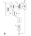
次に、本発明に係る信号補正回路200の第1実施形態について、図1を参照しつつ説明する。尚、図1では、信号補正回路200にて実行される各種信号補正のうち、輪郭補正に係る部分のみを示している。
Next, a first embodiment of a
上記デジタル映像信号S1は、フィルタ回路10に入力され、デジタル映像信号S1から所定の周波数成分、すなわち高周波成分である輪郭成分が抽出される。フィルタ回路10は、例えばタップ係数が可変のBPF(バンドパスフィルタ)或いはHPF(ハイパスフィルタ)で構成されており、このタップ係数を変更することにより、デジタル映像信号S1を一次微分または二次微分する。本実施形態においては、デジタル映像信号S1を二次微分して映像信号の輪郭成分を抽出するものとする(つまり映像信号の二次微分値を輪郭成分とする)。フィルタ回路10によって抽出された輪郭成分は、コアリング回路16によってコアリング処理され、ノイズ成分が抑圧もしくは除去される。コアリング回路16からの信号は、輪郭成分のレベルを可変するレベル可変回路である輪郭成分非線形処理部13及び絶対値化回路15に出力される。輪郭成分非線形処理部は、与えられた輪郭強調量に従い輪郭成分を増幅して加算器14へ出力する。加算器14は、元のデジタル映像信号S1と輪郭成分非線形処理部13により増幅された輪郭成分が入力され、これらを加算することにより輪郭補正(輪郭強調)された映像信号S2を出力する。この輪郭補正された映像信号S2は、上述のように図10の表示部300へ供給される。
The digital video signal S1 is input to the
一方、絶対値化回路15は、コアリング回路16によりコアリング処理された輪郭成分を絶対値化し、ヒストグラム検出回路11へ出力する。ヒストグラム検出回路11は、絶対値化回路15で絶対値化された輪郭成分を用いて、この輪郭成分のレベルに応じた出現度数、すなわちヒストグラムを求める。本実施形態においては、ヒストグラム検出回路11は、映像信号一画面分(例えば映像信号1フィールドもしくは1フレーム分。以下、単に「一画面分」と呼ぶ)において、予め定めた複数のレベル範囲の各々に属する輪郭成分の度数、すなわち各所定レベル範囲の含まれる輪郭成分に対応する画素数を算出することで、上記ヒストグラムを得るようにしている。ヒストグラム検出回路11によって検出された輪郭成分のヒストグラムは、制御回路12に供給される。制御回路12は、この検出された輪郭成分のヒストグラムに基づいて上記輪郭成分非線形処理部13の輪郭強調量を求め、該輪郭成分非線形処理部13の増幅率(ゲイン)を制御する。この様な構成によって、デジタル映像信号S1は、このデジタル映像信号S1に含まれる輪郭成分のヒストグラムに応じた輪郭補正(輪郭強調)が為される。
On the other hand, the absolute
上記ヒストグラム検出回路11における輪郭成分のヒストグラム検出動作の詳細について、図2を用いて以下に説明する。図2(a)は、水平1ライン分の絶対値化された輪郭成分の一例を示している。図2(a)に示されように、絶対値回路15で絶対値化された輪郭成分は、予め設定された複数の境界(EDGLEV0、EDGLEV1、EDGLEVmax)により分割された複数のレベル範囲(X0、X2、X3)のいずれかに含まれるものとする。本実施形態では、境界をEDGLEV0、EDGLEV1及びEDGLEVmaxの3つとして、分割レベル範囲(X0、X1、X2)を3つとしている。勿論、分割レベル範囲の数はこれよりも多くてもよく、実際には分割領域を8個とすることが望ましいが、ここでは説明の簡略化のために3つとしている。ヒストグラム検出回路11では、輪郭成分が上記分割レベル範囲(X0、X2、X3)のどれに属するかを、画素毎に、輪郭成分と上記境界(EDGLEV0、EDGLEV1、EDGLEVma)とをそれぞれ比較することにより判定する。ヒストグラム検出回路11は、上記分割レベル範囲に各々対応して割り当てられた複数のカウンタ(図示せず)を含んでいる。そしてヒストグラム検出回路11は、この複数のカウンタで、各分割レベル範囲に属する輪郭成分の画素を、分割レベル範囲毎に計数する。この分割レベル範囲毎の画素の計数は、映像信号の1フィールドもしくは1フレーム期間にわたって行われ、一画面分の各分割レベル範囲に含まれる画素数が積算される。これによって、図2(b)に示されるように、一画面における各分割レベル範囲(X0、X1、X2)毎の輪郭成分の出現度数、すなわち輪郭成分のヒストグラムが検出される。ここで一画面全体の総画素数をXとすると、X=X0 + X1 + X2と表されるものとする。
Details of the histogram detection operation of the contour component in the
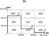
次に、制御回路12における具体的な輪郭成分非線形処理部13の制御について、図3及び図4を用いて説明する。制御回路12では、ヒストグラム検出回路11の検出結果を、図3に示されるような、振幅−画素マップ上にマッピングする。具体的には、横軸を輪郭成分の振幅(レベル)、縦軸を画素数とした2次元空間を、予め定められた3つの振幅境界(EDGLEV0、EDGLEV1、EDGLEVmax)及び3つの画素数境界(DOTLEV0、DOTLEV1、DOTLEVmax)で分割して9つのデータ領域(A00〜A02、A10〜A12、A20〜A22)を含む振幅−画素マップを設定する。尚、図2(b)に示されたレベル範囲X0は0〜DOTLEV0の範囲に、レベル範囲X1はDOTLEV0〜DOTLEV1の範囲に、レベル範囲X2はDOTLEV1〜DOTLEVmaxの範囲に相当する。そして、上記輪郭成分のヒストグラムの検出結果である各分割レベル範囲(X0、X1、X2)の画素数量が、各データ領域(A00〜A22)のどれに該当するかを判定して図3のようにマッピングする。ここでは、レベル範囲X0の画素数はデータ領域A02に、レベル範囲X1の画素数はデータ領域A10に、レベル範囲X2の画素数はデータ領域A20に該当するものとしている。
Next, specific control of the contour component
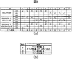
制御回路12は、上記にようにして得られた振幅−画素マップを用いて、図4(a)に示される制御テーブルを参照して輪郭成分非線形処理部13に対するゲインの制御量を算出する。この制御テーブルは、制御回路12の内部、もしくは制御回路12と接続される(図示しない)メモリに格納されている。また制御テーブルは、各分割レベル範囲(X0、X1、X2)の画素数に該当するデータ領域(以下、該当データ領域と呼ぶ)の組み合わせと、輪郭成分非線形処理部13に対するゲイン制御量との対応関係を記憶している。尚、上記該当データの組み合わせは、例えば総画素数Xを100、画素数境界DOTLEV0を30、DOTLEV1を60、DOTLEVmaxを100(=総画素数X)とすれば、全部で11通りとなる。本実施形態では、図4(a)に示されるように、この11通りの組み合わせパターンの各々に対応させて最適な制御量を予め設定している。この組み合わせパターンに対応する制御量は、任意に設定可能である。
Using the amplitude-pixel map obtained as described above, the
そして制御回路12は、図3に示された振幅−画素マップから該当データ領域の組み合わせを判定し、この組み合わせに対応する制御量を上記制御テーブルから読み出して輪郭成分非線形処理部13のゲインを制御する。図3の場合、制御回路12は、該当データ領域の組み合わせが〔A02、A10、A20〕であると判別する。この組み合わせパターンは、図4(a)のNo.11に該当する。従って、制御回路12は、図4(a)に示された制御テーブルからNo.11に対応する制御量、すなわち「小」を読み出し、図4(b)に示されるように、ゲイン増加量を小さくするか、ゲイン増加量をOFFとするように輪郭成分非線形処理部13を制御する。更に、制御量「小」の場合は、図4(b)に示されるように、NR(ノイズリダクション)回路を動作するように制御してもよい。また図4(b)に示されるように、制御テーブルから制御量「中」が選択された場合は、ゲイン増加量を中程度とし、制御テーブルから制御量「大」が選択された場合は、ゲイン増加量を大きくする。
Then, the
ここで、該当データ領域の組み合わせと制御量との対応付け方ついて、代表的なパターンを例にして説明する。図3のように、組み合わせパターンがNo.11に該当する場合は、低いレベル範囲X0の成分が最も多いため、振幅の小さい輪郭成分、すなわちノイズ成分を多く含んでいると考えられる。よって、この場合はゲインの制御量を「小」とし、ノイズ成分を増幅しないようにする。組み合わせパターンがNo.4に該当する場合は、中間のレベル範囲X1の成分が他の範囲よりも多いが、その振幅はあまり大きくないと考えられる。よって、この場合は輪郭がぼやけているものと考えられため、ゲインの制御量を「大」として輪郭をくっきりさせる。また組み合わせパターンがNo.1に該当する場合は、高いレベル範囲X2の成分が最も大きく、またその振幅も大きい。この場合は、既に輪郭がくっきりしている状態なので、ゲインの制御量を「小」として、過度の輪郭強調によるぎらつきを防止する。 Here, a method of associating the combination of the corresponding data area with the control amount will be described using a typical pattern as an example. As shown in FIG. 3, if the combination pattern corresponds to No.11, because components of the low level range X 0 is highest, low profile component amplitude, that is believed to contain more noise components. Therefore, in this case, the gain control amount is set to “small” so that the noise component is not amplified. If the combination pattern corresponds to No.4, although components of the intermediate level range X 1 is larger than the other range, its amplitude is considered not so large. Therefore, in this case, since the contour is considered to be blurred, the contour is sharpened by setting the gain control amount to “large”. Also if the combination pattern corresponds to No.1 is the largest component of the high level range X 2 is also the large amplitude. In this case, since the outline is already clear, the amount of gain control is set to “small” to prevent glare due to excessive outline enhancement.
以上の、該当データ領域の組み合わせと制御量との対応付けの説明は、あくまでも一例であり、各パターンにおいて想定される輪郭もしくはノイズの状況を考慮して任意に変更することができる。また、予め設定される制御量のレベルを大、中、小の3段階としたが、これよりも増やしてよいことは自明である。 The above description of the correspondence between the combination of the corresponding data area and the control amount is merely an example, and can be arbitrarily changed in consideration of the contour or noise situation assumed in each pattern. In addition, although the level of the control amount set in advance is set to three levels of large, medium, and small, it is obvious that it may be increased more than this.
次に上記輪郭成分非線形処理部13の詳細について、図11、図12を用いて説明する。図11に示されるように、輪郭成分非線形処理部13は水平垂直輪郭強調ゲイン制御部17及び非線形振幅リミッタ部18を含んでいる。図11の(a)、(b)、(c)の各点における入出力特性を各々図12(a)、(b)、(c)に示す。まず、コアリング回路16は、図12(a)に示されるように、不感帯(NCOR及び-NCOR)が設けられており、このNCOR(-NCOR)以下の入力信号に対する出力信号のレベルを0とする。これにより、NCOR(-NCOR)以下のレベルを持つ微小なノイズ成分が除去される。コアリング回路16によってノイズが除去された信号は、輪郭成分非線形処理部13内の水平垂直輪郭強調ゲイン制御部17に入力される。ゲイン制御部17は、制御回路12からの上記検出ヒストグラムに応じたゲイン制御量が与えられ、コアリング回路16からの信号のゲインを図12(b)に示されるように制御する。図12(b)において、GAIN=1は、例えば図4(a)に示された制御テーブルからゲイン制御量「中」が選択された場合の当該ゲイン制御部17の入出力特性であり、OUT=INとなる特性である。GAIN=2は、例えば上記制御テーブルからゲイン制御量「大」が選択された場合の当該ゲイン制御部17の入出力特性であり、OUT=2*INの特性である。図12(b)に示されるように、いずれの特性も線形であるが、GAIN=2(ゲイン制御量「大」)のときは、GAIN=1(ゲイン制御量「中」)のときよりも入出力特性の傾きを大きくし、より大きく輪郭成分の振幅を増幅するようにしている。GAIN=0は、例えば上記制御テーブルからゲイン制御量「小」が選択された場合の当該ゲイン制御部17の入出力特性である。この場合、どのようなレベルの入力信号でも出力信号のレベルは0となる。すなわち、この場合は輪郭成分のレベルは0となるため、輪郭強調は行われない。この例では、ゲイン制御量「小」のときは、GAIN=0として輪郭強調を行わないようにしているが、GAIN=1よりも小さく、かつGAIN=0よりも大きいゲイン(例えばGAIN=0.5)を与えて、若干輪郭強調をするようにしてもよい。上記GAIN=0、1、2の値は一例であり、これらの値は適宜変更可能である。
Next, details of the contour component
ゲイン制御部17によってゲインが制御された信号は、非線形振幅リミッタ部18に入力される。リミッタ部18は、小振幅の輪郭信号を強調するためにエンハンサゲインを強くした場合に有効である。以下、リミッタ部18の詳細について入力信号が8ビットのデジタル信号で、その最大値が255の場合を例にして説明する。リミッタ部18は、図12(c)に示されるように、例えば正負それぞれの領域において、上に凸の入出力特性と下に凸の入出力特性を持っており、以下では正領域のみの入出力特性を説明する。ここでは、負領域の入出力特性は正領域と対称としているため、その詳細な説明は省略する。リミッタ部18は、図12(c)に示されるように、例えば、互いに異なる値を持つ2つのリミッタ(LMT1=150、LMT2=200)を持ち、NCOR〜LMT1の範囲の傾きを1、LMT1〜LMT2の範囲の傾きを0、LMT2以降の傾きを−1としている。従って、入力信号INがNCOR<IN<LMT1である場合は、入力信号レベルの例して出力信号レベルが増加し、入力信号INがLMT1からLMT2の間にある場合、すなわち150≦IN≦200である場合は、出力信号のレベルが一定となる。そして、入力信号INがLMT2より大きい場合、すなわちLMT2<INの場合は、入力信号レベルの増加に比例して出力信号のレベルが減少する。このような構成によれば、ある一定レベルを超える大振幅の輪郭信号に対してその振幅レベルを一定もしくは下げるように制御するため、大振幅の輪郭信号を過度に強調することが防止される。このため、大振幅を持つ輪郭部について、その画質の破綻を回避することが可能となる。またLMT1=LMT2としてもよいし、LMTの数、傾きの制御は制御回路12によって任意に設定可能である。
The signal whose gain is controlled by the
このように、本実施形態では、各分割レベル範囲に含まれる輪郭成分の出現頻度、すなわち輪郭成分のヒストグラムを検出し、各分割レベル範囲の該当データ領域の組み合わせに応じて輪郭成分のレベルを制御している。従って、課題で例示したような、例えば白い背景と比較的暗色の単一物体とで構成された映像と、互いに輝度差や色差が少ない複数の物体で構成された映像との輪郭の状態を区別して、それぞれに適した輪郭補正を行うことが可能となる。 As described above, in this embodiment, the appearance frequency of the contour component included in each division level range, that is, the histogram of the contour component is detected, and the level of the contour component is controlled according to the combination of the corresponding data areas in each division level range. is doing. Therefore, the contour state between an image composed of, for example, a white background and a relatively dark single object, as exemplified in the subject, and an image composed of a plurality of objects with little brightness difference and color difference is distinguished. Separately, it is possible to perform contour correction suitable for each.
また、本実施形態においては、所定期間、たとえば映像信号の1フィールドもしくは1フレーム期間における輪郭成分のヒストグラムを検出して輪郭補正をしているので、輪郭成分非線形処理部13における輪郭補正の誤差を極力小さいものとすることができる。すなわち、本実施形態では、正確に映像の状態(映像に含まれる輪郭の状況)を判断して、より自然に近い輪郭強調の制御を行うことが可能である。尚、振幅補正される輪郭成分は、フィルタ回路10の通過帯域を変更することによって適宜選択可能である。従って、要求に応じて、比較的低周波の輪郭成分、及び比較的高周波の輪郭成分のいずれかを任意に選択して適宜補正することが可能である。
In the present embodiment, since the contour correction is performed by detecting the histogram of the contour component in a predetermined period, for example, one field or one frame period of the video signal, the contour correction error in the contour component
更にまた、本実施形態では、制御回路12において、振幅境界及び画素数境界をそれぞれ3つとし、9個のデータ領域を設定するものとしたが、これは説明を簡略化するためであり、当然ながらこれに限られるものではない。要求される輪郭補正の精度に応じて、振幅境界及び画素数境界、並びにデータ領域の数を任意に設定することが可能である。振幅境界及び画素数境界、並びにデータ領域の数を図3のものよりも増加させた振幅−画素マップの他の例を図5に示す。このようなマップを用いれば、より細かな、かつ滑らかな輪郭補正を行うことができる。従って、図5に示されるマップを用いれば、図3のものに比べ、より自然な画面表示を実現することが可能である。
Furthermore, in this embodiment, in the
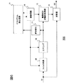
次に、本発明の第2実施形態について、図6を用いて説明する。図1に示された第1実施形態と異なる点は、フィルタ回路20及びコアリング回路16が制御回路12により制御可能とした点である。図1と同じ符号は同じ機能を有するものとしてその説明は省略する。
Next, a second embodiment of the present invention will be described with reference to FIG. The difference from the first embodiment shown in FIG. 1 is that the
図8において、フィルタ回路20は輪郭強調成分を入力映像信号より抽出するBPF(バンドパスフィルタ)であり、その通過周波数帯域が、制御回路12からの制御信号により可変される。制御回路12は、第1実施形態と同様に、ヒストグラム検出回路11の結果に応じて、輪郭成分非線形処理部13の輪郭強調量を制御するとともに、フィルタ回路20のフィルタ係数を制御し、その通過周波数帯域幅を制御する。
In FIG. 8, a
本実施形態では、フィルタ回路20の通過帯域を制御可能とすることで、入力映像信号の種類に応じて、ヒストグラム検出や輪郭補正に最適な通過帯域を選択できる。例えば、地上波アナログ放送のNTSC(National Television Standards Committee)信号と、地上波及び衛星デジタル放送のハイビジョン信号では、映像信号の周波数帯域が異なる。制御回路12は、テレビジョン放送を受信するチューナの種類(アナログチューナかデジタルチューナのどれを用いてテレビジョン信号の受信をしているか)、または入力映像信号の水平周波数等の、映像信号の種類を表す情報を検出し、その検出情報を用いてフィルタ回路20の通過周波数帯域を制御する。例えば、制御回路12は、NTSC受信時よりもデジタル放送受信時の方でフィルタ回路20の通過周波数帯域を広くもしくは高くするように制御する。これにより、入力映像信号に応じてフィルタ回路の通過周波数帯域を最適にすることが可能となる。よって、本実施形態では、映像信号種類に適した輪郭補正が可能となる。
In the present embodiment, the pass band of the
また、本実施形態では、フィルタ回路20を制御する以外に、コアリング回路16をも制御している。図4(b)に示されるように、制御量「小」が制御テーブルから選択された場合は、NR(ノイズリダクション)の効果を強くするか、もしくはNRの動作をONとするような制御も併せて行うようにしている。本実施形態は、このNRの制御を、コアリング回路16を制御することにより実行している。すなわち、図4(a)に示される制御テーブルにおいて制御量「小」が選択された場合は、制御回路12はコアリング回路16に対し制御信号を出力し、コアリング回路16によるノイズ抑圧または除去機能を高めるように制御する。例えば、図12(a)に示されるNCOR(-NCOR)の値を大きくして不感帯を広げるようにコアリング回路16を制御する。コアリング回路16のコアリング量が0(CORING=0)の場合は、これを所定値(>0)にしてノイズ抑圧または除去動作を開始させる。これにより、例えば輪郭成分のヒストグラムからノイズ成分が多い映像と判断された場合に、適切にノイズ成分を抑圧もしくは除去することができる。従って、本実施形態では、輪郭成分のヒストグラムに応じた適切なノイズ抑圧が可能となる。第1実施形態と組み合わせれば、ノイズ成分が多い映像において(例えば組み合わせパターンNo.11を選択した場合において)、ノイズ成分の増幅を抑えつつ、ノイズ成分を抑圧することが可能となる。
In the present embodiment, in addition to controlling the
次に、本発明の第3実施形態について、図7を用いて説明する。図1に示された第1実施形態と異なる点は、フィルタ回路とコアリング回路との組み合わせを、輪郭成分のヒストグラムを検出するためのものと、レベルを制御して映像信号に加算するためのものとの、2系統設けた点にある。図1及び図6と同じ符号は同じ機能を有するものとしてその説明は省略する。 Next, a third embodiment of the present invention will be described with reference to FIG. The difference from the first embodiment shown in FIG. 1 is that a combination of a filter circuit and a coring circuit is used to detect a histogram of contour components, and a level is controlled to be added to a video signal. It is in the point which provided two systems with the thing. The same reference numerals as those in FIGS. 1 and 6 have the same functions, and the description thereof is omitted.
図7において、第1フィルタ回路20は、輪郭成分を入力映像信号から抽出するBPF(バンドパスフィルタ)であり、ここで抽出された輪郭成分は輪郭成分非線形処理部13によりその振幅が制御されて加算器14により元の映像信号S1と加算される。一方、第2フィルタ回路30も、同様に輪郭成分を入力映像信号から抽出するBPF(バンドパスフィルタ)であるが、ここで抽出された輪郭成分はコアリング回路16、及び絶対値化回路15を介してヒストグラム検出回路11に供給される。第1のフィルタ回路20と第2のフィルタ回路30は、それぞれ、その通過周波数帯域が制御回路12により制御可能とされる。また、第1、第2のフィルタ回路20及び30には、それぞれコアリング回路16が接続されており、それぞれの系統においてノイズ抑圧処理が行われる。制御回路12は、第1実施形態と同様に、ヒストグラム検出回路11の結果に応じて、輪郭成分非線形処理部13の輪郭強調量を制御するととともに、第1、第2のフィルタ回路20及び30のフィルタ係数を制御し、その通過周波数帯域幅を制御する。更に、制御回路12は、2つのコアリング回路16を上述した第二実施形態のように制御して、輪郭成分のヒストグラムに応じたノイズ抑圧、除去処理を行う。
In FIG. 7, the
本実施形態では、輪郭補正用の第1のフィルタ回路20と、ヒストグラム検出用の第2のフィルタ回路30をそれぞれ用意することで、ヒストグラム検出を行う映像信号の周波数帯域と、輪郭補正を行う周波数帯域とをそれぞれ分けることができる。例えば、第2のフィルタ回路30の通過周波数帯域を第1のフィルタ回路20よりも広く設定する。制御回路12は、ヒストグラム検出回路11におけるヒストグラムの検出結果から、どの周波数成分の映像が多く含まれているか判断し、第1のフィルタ回路20の通過帯域をより効果的な通過帯域に制御する。本実施形態によれば、第2のフィルタ回路30の通過周波数帯域を広くしているので、画面全体の特徴をより正確に捉えることが可能となる。更に、輪郭補正用の第1のフィルタ回路20を設けているので、第2のフィルタ回路30で抽出される周波数帯域の信号の中から、輪郭補正を行いたい周波数成分の輪郭成分のみを振幅制御することが可能となる。また本実施形態では、制御回路12によって、第1のフィルタ回路20の通過周波数帯域を変更して輪郭補正させたい帯域のみをだけ通過することもできる。更にまた、制御回路12によって、第2のフィルタ回路30の通過周波数帯域を変更して、輪郭成分のヒストグラムの検出精度を変更することも可能となる。従って本実施形態によれば、より映像に適した輪郭補正が可能となる。
In this embodiment, by preparing the
尚、図7に示されるように、第1のフィルタ回路20で抽出された信号を、絶対値化回路15を介してヒストグラム検出回路11に供給してもよい。すなわち、第1のフィルタ回路20を、輪郭補正用のみでなく、ヒストグラム検出用に使用してもよい。この場合、異なる周波数帯域の輪郭成分についてヒストグラムを検出することが可能となるので、異なる種類の輪郭成分のヒストグラムを把握することが可能となる。従って、このようにすれば、周波数成分が異なる輪郭成分について、それぞれ適切な輪郭補正を行うことが可能となる。
As shown in FIG. 7, the signal extracted by the
次に、本発明の第4実施形態について、図8を用いて説明する。この第4実施形態は、図7に示された第3実施形態において、2つのコアリング回路16の出力いずれかを切り替えてヒストグラム検出回路11へ出力するスイッチ回路20を追加したものである。
Next, a fourth embodiment of the present invention will be described with reference to FIG. In the fourth embodiment, in the third embodiment shown in FIG. 7, a
ヒストグラム検出回路は、スイッチ回路20によって、第1のフィルタ回路20または第2のフィルタ回路30のいずれかの出力が入力される。また、スイッチ回路は、制御回路12からの制御信号により切り替え制御されるように構成されてもよい。これにより、異なる周波数成分の輪郭成分のいずれかを選択して輪郭補正をすることが可能となる。どちらを選択するかは、予め定めておいてもよいし、映像の状況に応じて、制御回路12により適宜切り替えるようにしてもよい。
The output of either the
次に、本発明の第5実施形態について、図9を用いて説明する。この第5実施形態は、図7に示された第3実施形態において、第2のフィルタ回路30、コアリング回路16及び絶対値回路15の組み合わせを複数系統としたものである。すなわち、第5実施形態は、ヒストグラム検出用の第2のフィルタ回路を複数用い、それぞれの通過周波数帯域を互いに異ならせることによって、より多くの周波数成分の輪郭成分を抽出することが可能となる。
Next, a fifth embodiment of the present invention will be described with reference to FIG. In the fifth embodiment, a combination of the
また、各第1のフィルタ回路30は、それぞれ制御回路12によりその通過周波数帯域が制御可能とされており、この制御は、ヒストグラム検出回路11の検出結果に応じて行うようにしている。各コアリング回路16も、第3及び第4実施形態と同様に、ヒストグラム検出回路11の検出結果に応じて制御回路12により制御されるように構成される。上記第1のフィルタ回路の1つを、例えば文字や図形情報を主体とした映像の輪郭成分を抽出するのに適した通過周波数帯域とし、他の1つを、例えば自然画を主体とした映像の輪郭成分を抽出するのに適した通過周波数帯域とする。これにより、表示内容が異なる映像に応じて、適切に輪郭成分を抽出することができるとともに、その輪郭補正を適切に行うことが可能となる。また、たとえばアナログ放送とデジタル放送とを表示部300に同時に表示する場合(いわゆる2画面表示)、上記第1のフィルタ回路の1つを、アナログ放送において映像の輪郭成分を抽出するのに適した通過周波数帯域とし、他の1つを、デジタル放送において映像の輪郭成分を抽出するのに適した通過周波数帯域とする。このようにすれば、映像信号の種類に応じて、適切に輪郭成分を抽出することができるとともに、その輪郭補正を適切に行うことが可能となる。
In addition, the pass frequency band of each
10…フィルタ回路、11…ヒストグラム検出回路、12…制御回路、13…輪郭成分非線形処理部、14…加算器、15…絶対値化回路、16…コアリング回路、17…水平垂直輪郭強調ゲイン制御部、18…非線形リミッタ部、20…スイッチ、21…制御回路、30…フィルタ回路、100…チューナ部、200…信号補正回路、300…表示部、400…駆動部
DESCRIPTION OF
Claims (5)
入力された映像信号に含まれる輪郭成分のヒストグラムを検出するヒストグラム検出部と、
前記ヒストグラム検出部で検出された前記輪郭成分のヒストグラムを用いて前記映像信号の輪郭成分を補正する輪郭補正部と、
前記ヒストグラム検出部で検出された前記輪郭成分のヒストグラムに基づき前記輪郭補正部を制御する制御部と、
前記輪郭補正部によって輪郭補正された映像信号に基づき映像を表示する表示部と、
を備え、
前記ヒストグラム検出部は、前記入力信号に含まれる複数の所定輪郭成分レベル毎に、前記輪郭成分の出現度数を取得して前記輪郭成分のヒストグラムを検出するように構成され、
前記制御部は、前記輪郭成分のヒストグラムから、前記各所定輪郭成分レベルにおける前記輪郭成分の出現度数の組み合わせを取得し、該組み合わせに基づいて、前記輪郭補正部における前記輪郭成分の補正量を制御することを特徴とする映像表示装置。 In the video display device,
A histogram detector for detecting a histogram of contour components included in the input video signal;
A contour correcting unit that corrects a contour component of the video signal using a histogram of the contour component detected by the histogram detecting unit;
A control unit that controls the contour correction unit based on a histogram of the contour component detected by the histogram detection unit;
A display unit for displaying a video based on the video signal whose contour has been corrected by the contour correction unit;
With
The histogram detection unit is configured to detect the histogram of the contour component by acquiring the appearance frequency of the contour component for each of a plurality of predetermined contour component levels included in the input signal;
The control unit acquires a combination of the appearance frequencies of the contour components at each predetermined contour component level from the contour component histogram, and controls the correction amount of the contour component in the contour correction unit based on the combination A video display device characterized by:
前記制御部は、前記組み合わせに応じて前記レベル可変回路を制御することを特徴とする請求項1に記載の映像表示装置。 2. The video display device according to claim 1, wherein the contour correction unit includes a filter circuit that extracts the contour component from the input video signal, and a level variable circuit that varies a level of the contour component extracted by the filter circuit. An adder that adds the contour component output from the level variable circuit and the input video signal;
The video display device according to claim 1, wherein the control unit controls the level variable circuit according to the combination.
前記輪郭成分のヒストグラムから得られた前記組み合わせに対応する前記制御量を前記制御テーブルから読み出し、該読み出された制御量に基づいて前記レベル可変回路を制御することを特徴とする映像表示装置。 The video display device according to claim 2, wherein the control unit includes a control table in which a correspondence relationship between the combination and a control amount for the level variable circuit is stored in advance.
An image display device, wherein the control amount corresponding to the combination obtained from the contour component histogram is read from the control table, and the level variable circuit is controlled based on the read control amount.
Priority Applications (6)
| Application Number | Priority Date | Filing Date | Title |
|---|---|---|---|
| JP2004185794A JP4155233B2 (en) | 2004-06-24 | 2004-06-24 | Video display device |
| GB0503605A GB2416085B (en) | 2004-06-24 | 2005-02-21 | Video display apparatus |
| GB0601497A GB2420670B (en) | 2004-06-24 | 2005-02-21 | Video display apparatus |
| CNB2007101524057A CN100515032C (en) | 2004-06-24 | 2005-02-22 | Video display apparatus |
| US11/061,826 US7430021B2 (en) | 2004-06-24 | 2005-02-22 | Video display apparatus having contour correction function |
| CNB2005100073944A CN100397870C (en) | 2004-06-24 | 2005-02-22 | Video display apparatus |
Applications Claiming Priority (1)
| Application Number | Priority Date | Filing Date | Title |
|---|---|---|---|
| JP2004185794A JP4155233B2 (en) | 2004-06-24 | 2004-06-24 | Video display device |
Related Child Applications (1)
| Application Number | Title | Priority Date | Filing Date |
|---|---|---|---|
| JP2007086372A Division JP4155328B2 (en) | 2007-03-29 | 2007-03-29 | Video display device |
Publications (3)
| Publication Number | Publication Date |
|---|---|
| JP2006013735A JP2006013735A (en) | 2006-01-12 |
| JP2006013735A5 JP2006013735A5 (en) | 2007-05-24 |
| JP4155233B2 true JP4155233B2 (en) | 2008-09-24 |
Family
ID=34420297
Family Applications (1)
| Application Number | Title | Priority Date | Filing Date |
|---|---|---|---|
| JP2004185794A Active JP4155233B2 (en) | 2004-06-24 | 2004-06-24 | Video display device |
Country Status (4)
| Country | Link |
|---|---|
| US (1) | US7430021B2 (en) |
| JP (1) | JP4155233B2 (en) |
| CN (2) | CN100397870C (en) |
| GB (2) | GB2416085B (en) |
Cited By (3)
| Publication number | Priority date | Publication date | Assignee | Title |
|---|---|---|---|---|
| US7930944B2 (en) | 2008-05-14 | 2011-04-26 | Honeywell International Inc. | ASIC compensated pressure sensor with soldered sense die attach |
| US8371176B2 (en) | 2011-01-06 | 2013-02-12 | Honeywell International Inc. | Media isolated pressure sensor |
| US8516897B1 (en) | 2012-02-21 | 2013-08-27 | Honeywell International Inc. | Pressure sensor |
Families Citing this family (15)
| Publication number | Priority date | Publication date | Assignee | Title |
|---|---|---|---|---|
| JP2006287636A (en) * | 2005-03-31 | 2006-10-19 | Pioneer Electronic Corp | Image quality adjustment apparatus, image quality adjustment method, and display apparatus |
| JP4946379B2 (en) * | 2006-11-16 | 2012-06-06 | パナソニック株式会社 | Image display apparatus, image display method, and computer program |
| US20080122857A1 (en) * | 2006-11-29 | 2008-05-29 | Chih-Lin Hsuan | Methods and devices for adjusting display characteristic of a video frame according to luminance statistics |
| JP4976836B2 (en) | 2006-12-13 | 2012-07-18 | エルジー ディスプレイ カンパニー リミテッド | Liquid crystal display |
| JP4861228B2 (en) * | 2007-03-30 | 2012-01-25 | 株式会社東芝 | Noise reduction device and noise reduction method |
| JP5002348B2 (en) * | 2007-06-26 | 2012-08-15 | 株式会社東芝 | Image processing apparatus, video receiving apparatus, and image processing method |
| JPWO2009037817A1 (en) * | 2007-09-19 | 2011-01-06 | パナソニック株式会社 | Contour correction device, contour correction method, and video display device |
| EP2198603A1 (en) * | 2007-10-01 | 2010-06-23 | Nxp B.V. | Pixel processing |
| JP2009201036A (en) * | 2008-02-25 | 2009-09-03 | Toshiba Corp | Video signal processing apparatus and video signal processing method |
| WO2010137387A1 (en) * | 2009-05-27 | 2010-12-02 | シャープ株式会社 | Image processing device and program |
| CN102612697B (en) * | 2009-07-21 | 2014-10-22 | 高通股份有限公司 | A method and system for detection and enhancement of video images |
| JP4762352B1 (en) * | 2010-03-17 | 2011-08-31 | 株式会社東芝 | Image processing apparatus and image processing method |
| JP4834776B2 (en) | 2010-03-17 | 2011-12-14 | 株式会社東芝 | Image processing apparatus and image processing method |
| KR101761415B1 (en) | 2010-11-25 | 2017-07-25 | 엘지디스플레이 주식회사 | Flat Panel Diaplay And Image Quality Control Method Thereof |
| JP2012244436A (en) * | 2011-05-19 | 2012-12-10 | Toshiba Corp | Video processing device and edge enhancement method |
Family Cites Families (28)
| Publication number | Priority date | Publication date | Assignee | Title |
|---|---|---|---|---|
| US4516167A (en) * | 1982-11-30 | 1985-05-07 | Rca Corporation | Compression of the dynamic range of video signals |
| DE3751412T2 (en) * | 1986-09-02 | 1995-12-14 | Fuji Photo Film Co Ltd | Method and device for image processing with gradation correction of the image signal. |
| JPH04100487A (en) * | 1990-08-20 | 1992-04-02 | Ikegami Tsushinki Co Ltd | Contour correcting method |
| US5592567A (en) * | 1992-11-10 | 1997-01-07 | Siemens Aktiengesellschaft | Method for detecting and separating the shadow of moving objects in a sequence of digital images |
| US5491520A (en) * | 1993-06-24 | 1996-02-13 | Victor Company Of Japan, Ltd. | Contour correcting circuit for sharpening rising and falling edges of video signals |
| JP2844514B2 (en) | 1993-11-26 | 1999-01-06 | 松下電器産業株式会社 | Television signal processor |
| JPH0846926A (en) | 1994-07-26 | 1996-02-16 | Toshiba Corp | Video signal processor |
| JP3221291B2 (en) | 1995-07-26 | 2001-10-22 | ソニー株式会社 | Image processing device, image processing method, noise elimination device, and noise elimination method |
| JPH0991419A (en) | 1995-09-25 | 1997-04-04 | Nec Corp | Image processor |
| JP3505017B2 (en) | 1995-10-23 | 2004-03-08 | 富士通株式会社 | Automatic method of contour enhancement or smoothing in image processing |
| JPH09163144A (en) | 1995-12-11 | 1997-06-20 | Fuji Photo Film Co Ltd | Method and device for processing image |
| JPH09307897A (en) | 1996-05-09 | 1997-11-28 | Fuji Photo Film Co Ltd | Image data compression processing method |
| KR0176601B1 (en) * | 1996-05-21 | 1999-05-01 | 김광호 | Picture quality improving method & circuit using low-filtering and histogram equalization |
| JPH1065935A (en) | 1996-08-21 | 1998-03-06 | Sony Corp | Video camera |
| KR100230391B1 (en) | 1996-11-29 | 1999-11-15 | 윤종용 | Method for correcting contour components of luminance signal and circuit thereof |
| JPH10191100A (en) * | 1996-12-26 | 1998-07-21 | Fujitsu Ltd | Video signal processing method |
| JPH1132201A (en) * | 1997-07-09 | 1999-02-02 | Matsushita Electric Ind Co Ltd | Image processing unit |
| DE69838779D1 (en) * | 1997-08-26 | 2008-01-10 | Matsushita Electric Ind Co Ltd | CORRECTION DEVICE FOR VERTICAL CONTOURS |
| JP3326377B2 (en) | 1997-12-12 | 2002-09-24 | シャープ株式会社 | Image quality correction circuit |
| JP3546691B2 (en) * | 1998-04-03 | 2004-07-28 | 松下電器産業株式会社 | Contour correction circuit |
| JP3097034B1 (en) | 1999-06-30 | 2000-10-10 | アンリツ株式会社 | Signal analyzer |
| JP2001078222A (en) | 1999-09-08 | 2001-03-23 | Matsushita Electric Ind Co Ltd | Video display device and control method therefor |
| JP2002290773A (en) | 2001-03-23 | 2002-10-04 | Sharp Corp | Image enhancing device and image enhancing program |
| EP1359747A4 (en) * | 2001-05-11 | 2007-07-18 | Matsushita Electric Ind Co Ltd | Video signal contour corrector |
| JP2004007202A (en) | 2002-05-31 | 2004-01-08 | Fuji Photo Film Co Ltd | Image processor |
| JP4169188B2 (en) | 2002-06-03 | 2008-10-22 | 株式会社K−Will | Image processing method |
| JP2004128643A (en) | 2002-09-30 | 2004-04-22 | Matsushita Electric Ind Co Ltd | Method for compensating tilt of image |
| JP4042615B2 (en) * | 2003-04-17 | 2008-02-06 | 株式会社デンソー | Image processing method and image processing apparatus |
-
2004
- 2004-06-24 JP JP2004185794A patent/JP4155233B2/en active Active
-
2005
- 2005-02-21 GB GB0503605A patent/GB2416085B/en active Active
- 2005-02-21 GB GB0601497A patent/GB2420670B/en active Active
- 2005-02-22 CN CNB2005100073944A patent/CN100397870C/en active Active
- 2005-02-22 US US11/061,826 patent/US7430021B2/en active Active
- 2005-02-22 CN CNB2007101524057A patent/CN100515032C/en active Active
Cited By (3)
| Publication number | Priority date | Publication date | Assignee | Title |
|---|---|---|---|---|
| US7930944B2 (en) | 2008-05-14 | 2011-04-26 | Honeywell International Inc. | ASIC compensated pressure sensor with soldered sense die attach |
| US8371176B2 (en) | 2011-01-06 | 2013-02-12 | Honeywell International Inc. | Media isolated pressure sensor |
| US8516897B1 (en) | 2012-02-21 | 2013-08-27 | Honeywell International Inc. | Pressure sensor |
Also Published As
| Publication number | Publication date |
|---|---|
| CN100397870C (en) | 2008-06-25 |
| CN101179652A (en) | 2008-05-14 |
| CN1713694A (en) | 2005-12-28 |
| US20050285977A1 (en) | 2005-12-29 |
| GB0503605D0 (en) | 2005-03-30 |
| GB2416085B (en) | 2006-11-29 |
| GB0601497D0 (en) | 2006-03-08 |
| JP2006013735A (en) | 2006-01-12 |
| GB2420670B (en) | 2007-01-03 |
| US7430021B2 (en) | 2008-09-30 |
| GB2420670A (en) | 2006-05-31 |
| GB2416085A (en) | 2006-01-11 |
| CN100515032C (en) | 2009-07-15 |
Similar Documents
| Publication | Publication Date | Title |
|---|---|---|
| JP4155233B2 (en) | Video display device | |
| JP4200890B2 (en) | Video signal processing apparatus, television receiver using the same, and video signal processing method | |
| JP4419933B2 (en) | Image processing apparatus, image display apparatus, and image processing method | |
| US20050185071A1 (en) | Image signal processing apparatus | |
| US8670079B2 (en) | Video display device | |
| JP4155328B2 (en) | Video display device | |
| EP1858253B1 (en) | Image correction circuit, image correction method and image display | |
| KR20080022633A (en) | Image processing apparatus, display apparatus comprising image processing apparatus and image processing method | |
| US7609282B2 (en) | Image display method and apparatus | |
| JP2006304352A (en) | Image processor | |
| JP4605654B2 (en) | Video signal processing device and display device equipped with the same | |
| JP4762336B2 (en) | Video processing apparatus and video processing method | |
| US8134646B2 (en) | Video signal processing device and video signal processing method | |
| EP1933556A2 (en) | TV user interface and processing for personal video players | |
| JPH06169437A (en) | Television receiver | |
| JP2009010517A (en) | Image processor, video receiver and image processing method | |
| US8351734B2 (en) | Video signal processing device and video display device | |
| JP4174656B2 (en) | Image display device, image processing device, and image processing method | |
| JP2004266757A (en) | Image processing apparatus and method | |
| EP1758370A2 (en) | Image processing apparatus, image display and image processing method | |
| EP2228993A1 (en) | Image processing apparatus and control method thereof | |
| JPH11355608A (en) | Monitor device and video signal transmitting device | |
| JP2012023543A (en) | Video processing apparatus and video processing method | |
| JP2012010077A (en) | Image quality improving device and method thereof | |
| JP2005223848A (en) | Contour emphasis circuit and contour emphasis method |
Legal Events
| Date | Code | Title | Description |
|---|---|---|---|
| RD04 | Notification of resignation of power of attorney |
Free format text: JAPANESE INTERMEDIATE CODE: A7424 Effective date: 20060424 |
|
| A521 | Request for written amendment filed |
Free format text: JAPANESE INTERMEDIATE CODE: A523 Effective date: 20070329 |
|
| A621 | Written request for application examination |
Free format text: JAPANESE INTERMEDIATE CODE: A621 Effective date: 20070329 |
|
| A977 | Report on retrieval |
Free format text: JAPANESE INTERMEDIATE CODE: A971007 Effective date: 20080313 |
|
| A131 | Notification of reasons for refusal |
Free format text: JAPANESE INTERMEDIATE CODE: A131 Effective date: 20080325 |
|
| A521 | Request for written amendment filed |
Free format text: JAPANESE INTERMEDIATE CODE: A523 Effective date: 20080521 |
|
| TRDD | Decision of grant or rejection written | ||
| A01 | Written decision to grant a patent or to grant a registration (utility model) |
Free format text: JAPANESE INTERMEDIATE CODE: A01 Effective date: 20080617 |
|
| A01 | Written decision to grant a patent or to grant a registration (utility model) |
Free format text: JAPANESE INTERMEDIATE CODE: A01 |
|
| A61 | First payment of annual fees (during grant procedure) |
Free format text: JAPANESE INTERMEDIATE CODE: A61 Effective date: 20080630 |
|
| FPAY | Renewal fee payment (event date is renewal date of database) |
Free format text: PAYMENT UNTIL: 20110718 Year of fee payment: 3 |
|
| R151 | Written notification of patent or utility model registration |
Ref document number: 4155233 Country of ref document: JP Free format text: JAPANESE INTERMEDIATE CODE: R151 |
|
| FPAY | Renewal fee payment (event date is renewal date of database) |
Free format text: PAYMENT UNTIL: 20110718 Year of fee payment: 3 |
|
| FPAY | Renewal fee payment (event date is renewal date of database) |
Free format text: PAYMENT UNTIL: 20110718 Year of fee payment: 3 |
|
| FPAY | Renewal fee payment (event date is renewal date of database) |
Free format text: PAYMENT UNTIL: 20120718 Year of fee payment: 4 |
|
| FPAY | Renewal fee payment (event date is renewal date of database) |
Free format text: PAYMENT UNTIL: 20130718 Year of fee payment: 5 |
|
| S111 | Request for change of ownership or part of ownership |
Free format text: JAPANESE INTERMEDIATE CODE: R313111 |
|
| R350 | Written notification of registration of transfer |
Free format text: JAPANESE INTERMEDIATE CODE: R350 |
|
| S111 | Request for change of ownership or part of ownership |
Free format text: JAPANESE INTERMEDIATE CODE: R313111 |
|
| R350 | Written notification of registration of transfer |
Free format text: JAPANESE INTERMEDIATE CODE: R350 |
|
| R250 | Receipt of annual fees |
Free format text: JAPANESE INTERMEDIATE CODE: R250 |
|
| R250 | Receipt of annual fees |
Free format text: JAPANESE INTERMEDIATE CODE: R250 |
|
| R250 | Receipt of annual fees |
Free format text: JAPANESE INTERMEDIATE CODE: R250 |
|
| R250 | Receipt of annual fees |
Free format text: JAPANESE INTERMEDIATE CODE: R250 |
|
| S111 | Request for change of ownership or part of ownership |
Free format text: JAPANESE INTERMEDIATE CODE: R313111 |
|
| R350 | Written notification of registration of transfer |
Free format text: JAPANESE INTERMEDIATE CODE: R350 |
|
| R250 | Receipt of annual fees |
Free format text: JAPANESE INTERMEDIATE CODE: R250 |
|
| R250 | Receipt of annual fees |
Free format text: JAPANESE INTERMEDIATE CODE: R250 |