JP4147187B2 - Manufacturing method of color image sensor on transparent substrate - Google Patents
Manufacturing method of color image sensor on transparent substrate Download PDFInfo
- Publication number
- JP4147187B2 JP4147187B2 JP2003523013A JP2003523013A JP4147187B2 JP 4147187 B2 JP4147187 B2 JP 4147187B2 JP 2003523013 A JP2003523013 A JP 2003523013A JP 2003523013 A JP2003523013 A JP 2003523013A JP 4147187 B2 JP4147187 B2 JP 4147187B2
- Authority
- JP
- Japan
- Prior art keywords
- substrate
- wafer
- layer
- color filter
- image sensor
- Prior art date
- Legal status (The legal status is an assumption and is not a legal conclusion. Google has not performed a legal analysis and makes no representation as to the accuracy of the status listed.)
- Expired - Fee Related
Links
- 239000000758 substrate Substances 0.000 title claims description 66
- 238000004519 manufacturing process Methods 0.000 title claims description 15
- 239000004065 semiconductor Substances 0.000 claims description 21
- 238000000151 deposition Methods 0.000 claims description 9
- 238000001514 detection method Methods 0.000 claims description 9
- 238000000034 method Methods 0.000 claims description 9
- 238000005520 cutting process Methods 0.000 claims description 4
- 239000011521 glass Substances 0.000 claims description 4
- 239000004033 plastic Substances 0.000 claims description 4
- 239000002178 crystalline material Substances 0.000 claims description 2
- 235000012431 wafers Nutrition 0.000 description 54
- 239000010703 silicon Substances 0.000 description 34
- 229910052710 silicon Inorganic materials 0.000 description 34
- XUIMIQQOPSSXEZ-UHFFFAOYSA-N Silicon Chemical compound [Si] XUIMIQQOPSSXEZ-UHFFFAOYSA-N 0.000 description 33
- 239000011159 matrix material Substances 0.000 description 8
- 238000002513 implantation Methods 0.000 description 7
- UFHFLCQGNIYNRP-UHFFFAOYSA-N Hydrogen Chemical compound [H][H] UFHFLCQGNIYNRP-UHFFFAOYSA-N 0.000 description 6
- 229910052739 hydrogen Inorganic materials 0.000 description 6
- 239000001257 hydrogen Substances 0.000 description 6
- 239000000126 substance Substances 0.000 description 6
- 238000005530 etching Methods 0.000 description 5
- 238000012545 processing Methods 0.000 description 5
- 238000002347 injection Methods 0.000 description 4
- 239000007924 injection Substances 0.000 description 4
- 230000035945 sensitivity Effects 0.000 description 4
- 230000008021 deposition Effects 0.000 description 3
- 229910052751 metal Inorganic materials 0.000 description 3
- 239000002184 metal Substances 0.000 description 3
- 238000000926 separation method Methods 0.000 description 3
- 229910052782 aluminium Inorganic materials 0.000 description 2
- XAGFODPZIPBFFR-UHFFFAOYSA-N aluminium Chemical compound [Al] XAGFODPZIPBFFR-UHFFFAOYSA-N 0.000 description 2
- 238000012993 chemical processing Methods 0.000 description 2
- 239000013078 crystal Substances 0.000 description 2
- 238000010438 heat treatment Methods 0.000 description 2
- 239000012535 impurity Substances 0.000 description 2
- 238000003754 machining Methods 0.000 description 2
- 239000000463 material Substances 0.000 description 2
- 239000004642 Polyimide Substances 0.000 description 1
- 239000000853 adhesive Substances 0.000 description 1
- 230000001070 adhesive effect Effects 0.000 description 1
- 239000000919 ceramic Substances 0.000 description 1
- 238000010028 chemical finishing Methods 0.000 description 1
- 238000004140 cleaning Methods 0.000 description 1
- 239000003086 colorant Substances 0.000 description 1
- 238000007796 conventional method Methods 0.000 description 1
- 230000007797 corrosion Effects 0.000 description 1
- 238000005260 corrosion Methods 0.000 description 1
- 230000007423 decrease Effects 0.000 description 1
- 230000007547 defect Effects 0.000 description 1
- 238000009792 diffusion process Methods 0.000 description 1
- 238000005516 engineering process Methods 0.000 description 1
- 238000007689 inspection Methods 0.000 description 1
- 238000004806 packaging method and process Methods 0.000 description 1
- 238000002161 passivation Methods 0.000 description 1
- 230000010287 polarization Effects 0.000 description 1
- 238000005498 polishing Methods 0.000 description 1
- 229920001721 polyimide Polymers 0.000 description 1
- 230000000135 prohibitive effect Effects 0.000 description 1
- 150000003376 silicon Chemical class 0.000 description 1
- 238000005476 soldering Methods 0.000 description 1
- 239000000243 solution Substances 0.000 description 1
Images


Classifications
-
- H—ELECTRICITY
- H01—ELECTRIC ELEMENTS
- H01L—SEMICONDUCTOR DEVICES NOT COVERED BY CLASS H10
- H01L27/00—Devices consisting of a plurality of semiconductor or other solid-state components formed in or on a common substrate
- H01L27/14—Devices consisting of a plurality of semiconductor or other solid-state components formed in or on a common substrate including semiconductor components sensitive to infrared radiation, light, electromagnetic radiation of shorter wavelength or corpuscular radiation and specially adapted either for the conversion of the energy of such radiation into electrical energy or for the control of electrical energy by such radiation
- H01L27/144—Devices controlled by radiation
- H01L27/146—Imager structures
-
- H—ELECTRICITY
- H01—ELECTRIC ELEMENTS
- H01L—SEMICONDUCTOR DEVICES NOT COVERED BY CLASS H10
- H01L31/00—Semiconductor devices sensitive to infrared radiation, light, electromagnetic radiation of shorter wavelength or corpuscular radiation and specially adapted either for the conversion of the energy of such radiation into electrical energy or for the control of electrical energy by such radiation; Processes or apparatus specially adapted for the manufacture or treatment thereof or of parts thereof; Details thereof
- H01L31/18—Processes or apparatus specially adapted for the manufacture or treatment of these devices or of parts thereof
- H01L31/1892—Processes or apparatus specially adapted for the manufacture or treatment of these devices or of parts thereof methods involving the use of temporary, removable substrates
-
- H—ELECTRICITY
- H01—ELECTRIC ELEMENTS
- H01L—SEMICONDUCTOR DEVICES NOT COVERED BY CLASS H10
- H01L27/00—Devices consisting of a plurality of semiconductor or other solid-state components formed in or on a common substrate
- H01L27/14—Devices consisting of a plurality of semiconductor or other solid-state components formed in or on a common substrate including semiconductor components sensitive to infrared radiation, light, electromagnetic radiation of shorter wavelength or corpuscular radiation and specially adapted either for the conversion of the energy of such radiation into electrical energy or for the control of electrical energy by such radiation
- H01L27/144—Devices controlled by radiation
- H01L27/146—Imager structures
- H01L27/14601—Structural or functional details thereof
- H01L27/1464—Back illuminated imager structures
-
- H—ELECTRICITY
- H01—ELECTRIC ELEMENTS
- H01L—SEMICONDUCTOR DEVICES NOT COVERED BY CLASS H10
- H01L27/00—Devices consisting of a plurality of semiconductor or other solid-state components formed in or on a common substrate
- H01L27/14—Devices consisting of a plurality of semiconductor or other solid-state components formed in or on a common substrate including semiconductor components sensitive to infrared radiation, light, electromagnetic radiation of shorter wavelength or corpuscular radiation and specially adapted either for the conversion of the energy of such radiation into electrical energy or for the control of electrical energy by such radiation
- H01L27/144—Devices controlled by radiation
- H01L27/146—Imager structures
- H01L27/14643—Photodiode arrays; MOS imagers
- H01L27/14645—Colour imagers
-
- H—ELECTRICITY
- H01—ELECTRIC ELEMENTS
- H01L—SEMICONDUCTOR DEVICES NOT COVERED BY CLASS H10
- H01L31/00—Semiconductor devices sensitive to infrared radiation, light, electromagnetic radiation of shorter wavelength or corpuscular radiation and specially adapted either for the conversion of the energy of such radiation into electrical energy or for the control of electrical energy by such radiation; Processes or apparatus specially adapted for the manufacture or treatment thereof or of parts thereof; Details thereof
- H01L31/02—Details
- H01L31/0216—Coatings
- H01L31/02161—Coatings for devices characterised by at least one potential jump barrier or surface barrier
- H01L31/02162—Coatings for devices characterised by at least one potential jump barrier or surface barrier for filtering or shielding light, e.g. multicolour filters for photodetectors
-
- Y—GENERAL TAGGING OF NEW TECHNOLOGICAL DEVELOPMENTS; GENERAL TAGGING OF CROSS-SECTIONAL TECHNOLOGIES SPANNING OVER SEVERAL SECTIONS OF THE IPC; TECHNICAL SUBJECTS COVERED BY FORMER USPC CROSS-REFERENCE ART COLLECTIONS [XRACs] AND DIGESTS
- Y02—TECHNOLOGIES OR APPLICATIONS FOR MITIGATION OR ADAPTATION AGAINST CLIMATE CHANGE
- Y02E—REDUCTION OF GREENHOUSE GAS [GHG] EMISSIONS, RELATED TO ENERGY GENERATION, TRANSMISSION OR DISTRIBUTION
- Y02E10/00—Energy generation through renewable energy sources
- Y02E10/50—Photovoltaic [PV] energy
Description
本発明は電子画像センサ、特に携帯電話に組み込まれるような小型カメラの製造を可能にする寸法の、非常に小さなサイズのセンサに関する。 The present invention relates to an electronic image sensor, in particular a sensor of very small size, dimensioned to allow the production of a miniature camera such as that incorporated into a mobile phone.
非常に小型であるだけでなく、この種の画像センサは、弱い光の下でも高感度を有し、高い測色性能を有しているべきである。
さらに、価格が法外にならないように最も経済的な方法でカメラ全体を製造する必要がある。
このことを達成するために、第一に、画像センサと電子処理回路を、可能であれば同じシリコン基板上に製造することが求められ、第二に、様々な層の堆積、エッチング、熱処理作業等を、同一のセンサを多数含むシリコンウェハ上で可能な限り集約的に行い、次いで該ウェハを独立したセンサに切り分けることが求められる。
しかし、これまでに提案されてきたカラー画像センサの製造方法及びそれらセンサの構造は、この点から見て完全に満足のいくものではない。その製造方法は産業上効果的でなく;依然として非常に高価であり、大量生産に適用するには効率が低すぎ、そうでない場合は、画像センサの性能が十分でない。
In addition to being very small, this type of image sensor should have high sensitivity even under low light and high colorimetric performance.
Furthermore, it is necessary to manufacture the entire camera in the most economical way so that the price is not prohibitive.
In order to achieve this, firstly the image sensor and the electronic processing circuit are required to be manufactured on the same silicon substrate if possible, and secondly, various layer deposition, etching and heat treatment operations. Etc. are performed as intensively as possible on a silicon wafer containing many identical sensors, and the wafer is then cut into independent sensors.
However, the color image sensor manufacturing methods and the structures of the sensors proposed so far are not completely satisfactory in this respect. The manufacturing method is not industrially effective; it is still very expensive and is too inefficient for mass production applications, otherwise the performance of the image sensor is not sufficient.
本発明は、高い品質と、特に優れた小型性、高感度及び高い測色性能を提示しつつも製造コストを最小限に抑える製造方法と、それに対応する画像センサを提案する。 The present invention proposes a manufacturing method for minimizing the manufacturing cost while presenting high quality, particularly excellent compactness, high sensitivity, and high colorimetric performance, and an image sensor corresponding thereto.
このために、本発明は:
−半導体ウェハの前面に、画像検出回路を備え且つそれぞれが各画像センサに対応する一連の活性領域を形成することと、ここで各活性領域は入力/出力パッドに囲まれている
−ウェハの前面を仮の支持基板の前面に対して移載することと、
−画像検出回路を備える薄い半導体層を基板に残して、半導体ウェハの厚さの大部分を除去すること
からなり、
−第一に、このようにして薄化された半導体層上に、カラーフィルタ層を堆積させ、次いでエッチングすることと、
−第二に、該カラーフィルタのエッチング後、仮基板及びウェハ全体の、カラーフィルタを支える側を、透過性の最終基板に移載することと、
−次いで、仮基板の少なくとも大部分を除去し、入力/出力パッドへのアクセスを容易にすることと、
−最後に、基板を個々のセンサに切り分けること
を特徴とする画像センサの製造方法を提案する。
To this end, the present invention:
-Forming a series of active areas on the front side of the semiconductor wafer with image detection circuits, each corresponding to each image sensor, wherein each active area is surrounded by input / output pads-front side of the wafer To the front surface of the temporary support substrate,
-Removing a majority of the thickness of the semiconductor wafer, leaving a thin semiconductor layer with image detection circuitry on the substrate;
Firstly depositing a color filter layer on the semiconductor layer thus thinned and then etching;
-Second, after etching the color filter, transferring the side of the temporary substrate and the whole wafer that supports the color filter to the transmissive final substrate;
-Then removing at least most of the temporary substrate to facilitate access to the input / output pads;
-Finally, a method for manufacturing an image sensor, characterized in that the substrate is cut into individual sensors, is proposed.
薄化された層の半導体材料は単結晶材料であるのが好ましく、最も一般的な可視光下での用途の場合は特にシリコンが好ましい。
仮基板は、センサを外部へ接続できる入力/出力パッドが露出されるように完全に除去されてよい。しかし、半導体ウェハを保護する薄層が残るように部分的にのみ除去することもできる。この場合、該薄層には、入力/出力パッドにアクセスするための孔を形成する必要がある。
The semiconductor material of the thinned layer is preferably a single crystal material, and silicon is particularly preferred for the most common applications under visible light.
The temporary substrate may be completely removed so that the input / output pads that can connect the sensor to the outside are exposed. However, it can also be removed only partially so that a thin layer protecting the semiconductor wafer remains. In this case, it is necessary to form a hole in the thin layer for accessing the input / output pad.
好適には、活性領域は感光要素のマトリクスを備え、さらに該マトリクスの制御回路と、活性領域の感光要素から発される信号を受信する、それに関連する画像処理回路を備える。このようにマトリクスと関連する回路は、マトリクスだけが光に曝されるようにアルミニウム層によって光から遮断されるのが好ましい。該アルミニウム層は透過性基板上に形成される。 Preferably, the active area comprises a matrix of photosensitive elements and further includes a control circuit for the matrix and associated image processing circuitry for receiving signals emitted from the photosensitive elements in the active area. Thus, the circuitry associated with the matrix is preferably shielded from light by the aluminum layer so that only the matrix is exposed to light. The aluminum layer is formed on a transmissive substrate.
仮基板への半導体ウェハの移載は、接着、標準的なはんだ付け、陽極ボンディング、又は単純に分子レベルで密着させることにより(つまり、良好な平坦性を有する2つの表面間での非常に強い接触力を介して)行うことができる。仮基板から最終基板への移載は、ボンディング又は分子レベルで密着させることにより行われるのが好ましいであろう。
基板への移載後且つフィルタの堆積前に、半導体ウェハの薄化を多くの様々な方法:ラッピングによる薄化、化学的な薄化、両方のタイプの薄化の組合せ(まず機械的な薄化を施し続いて化学的な仕上げ、又は化学薬品の存在下での機械加工)で行うことができる。薄化は、所望の切り分けレベルでウェハを予め脆化することによって、特に所望の切り分け面での深さ方向への水素注入によっても行うことができる。この場合、水素注入は、基板へのウェハの移載前、半導体ウェハに浅く行われる。次いで、基板と接触する薄い半導体層を残して、注入された切り分け面のレベルでウェハを分離する熱処理によって、薄化が行われる。
ウェハの非常に良好な薄化により、移載前は数百マイクロメートルだったその厚さが、基板への移載後は3ないし20マイクロメートルに減る。薄化は、測色性能と感度を向上させるため、センサの品質における重要な要因である。薄化されていないセンサで、画像検出回路を定義する複数の絶縁及び導電層が形成されている側から光が照射されると、カラーフィルタを横断した光は、異なる色に対応する感光ドットに散乱され、測色性能が低下する。さらに、薄いセンサでは、薄化されていないセンサの場合よりも光子がより広いシリコン領域に到達するため、感度が向上する。これは、光子が、各感光ドットに対応する表面領域の大部分を占める不透過性の金属層によっては遮断されないからである。
Transfer of a semiconductor wafer to a temporary substrate can be accomplished by bonding, standard soldering, anodic bonding, or simply adhesion at the molecular level (ie, very strong between two surfaces with good flatness) Via contact force). The transfer from the temporary substrate to the final substrate is preferably performed by bonding or adhesion at the molecular level.
After transfer to the substrate and before filter deposition, semiconductor wafer thinning can be done in many different ways: thinning by lapping, chemical thinning, a combination of both types of thinning (first mechanical thinning). Followed by chemical finishing or machining in the presence of chemicals). Thinning can also be performed by embrittlement of the wafer in advance at the desired cutting level, in particular by hydrogen implantation in the depth direction at the desired cutting surface. In this case, the hydrogen implantation is shallowly performed on the semiconductor wafer before the wafer is transferred to the substrate. Thinning is then performed by a heat treatment that separates the wafer at the level of the implanted slicing plane, leaving a thin semiconductor layer in contact with the substrate.
The very good thinning of the wafer reduces its thickness from several hundred micrometers before transfer to 3 to 20 micrometers after transfer to the substrate. Thinning is an important factor in sensor quality because it improves colorimetric performance and sensitivity. When light is irradiated from the side where a plurality of insulating and conductive layers defining the image detection circuit are formed by a non-thinned sensor, the light that has crossed the color filter is applied to photosensitive dots corresponding to different colors. Scattered and colorimetric performance decreases. Furthermore, the sensitivity of the thin sensor is improved because the photons reach a wider silicon region than in the case of a non-thinned sensor. This is because photons are not blocked by an impermeable metal layer occupying most of the surface area corresponding to each photosensitive dot.
しかしながら、薄化後、シリコンは剛性を失い非常に脆くなるので、薄化によって製造における問題が複雑化することと、さらには画像検出回路と外部を接続する問題が生じることが理解されるであろう。本発明の解決策は、この難題を軽減し、効率の高い画像センサの製造を可能にするものである。 However, after thinning, silicon loses rigidity and becomes very brittle, so it is understood that thinning complicates manufacturing problems and also causes problems connecting the image detection circuit to the outside. Let's go. The solution of the present invention alleviates this challenge and allows for the production of highly efficient image sensors.
最終的なセンサにおいて、光は透過性の最終基板を通って受け取られ、接続パッドはそれと反対側に配置されており、よって該センサはフリップチップ技術(ここで、該接続パッドを有するチップは、プリント回路基板に対して上下逆である)で取り付けることができる。透過性基板(ガラス又はプラスチック製)を通る光の損失は少ない。
最終基板とシリコン層は密着するので、ウェハの能動回路要素は良好に保護される。
例えば、直径15ないし20センチメートルの基板の場合、最終基板の厚さは約500マイクロメートルであり;シリコンウェハの厚さは、薄化前は(直径15ないし30センチメートルで)500ないし1000マイクロメートルで、薄化後は3ないし20マイクロメートルである。
シリコンウェハを中間基板に移載する前、且つ該中間基板を最終基板に移載する前に、例えばポリイミドから作られた平坦化層がシリコンウェハ上に堆積されてもよい。
特定の場合、中間基板は、一回分の製造に使用した後、また別の回に再使用できることに注意されたい。
In the final sensor, light is received through the transmissive final substrate and the connection pads are placed on the opposite side, so the sensor is flip-chip technology (where the chip with the connection pads is It can be mounted upside down with respect to the printed circuit board. There is little loss of light through the transmissive substrate (made of glass or plastic).
Since the final substrate and the silicon layer are in intimate contact, the active circuit elements of the wafer are well protected.
For example, for a substrate with a diameter of 15-20 centimeters, the final substrate thickness is about 500 micrometers; the thickness of the silicon wafer is 500-1000 micrometers (with a diameter of 15-30 centimeters) before thinning. In meters, 3 to 20 micrometers after thinning.
Before transferring the silicon wafer to the intermediate substrate and before transferring the intermediate substrate to the final substrate, a planarizing layer made of, for example, polyimide may be deposited on the silicon wafer.
It should be noted that in certain cases, the intermediate substrate can be reused for another time after it has been used for one manufacturing.
従って、本発明の目的は、光が、感光領域のマトリクスアレイに到達する前に導電層の体系に接触することなく、透過性基板、カラーフィルタ、感光半導体領域、次いで、絶縁及び導電層のスタックの順序でそれらを通過するように、モザイク状カラーフィルタと、感光領域のマトリクスアレイが形成されている非常に薄い単結晶半導体層(最大厚さが数十マイクロメートル)と、透過性基板を介した感光領域の照射により生成された電荷の収集を可能にする絶縁及び導電層のスタックとが上部に連続的に重畳されている透過性基板を備える画像センサである。
透過性基板は、ガラス又はプラスチック製であるのが好ましいが、セラミック又は結晶性物質から作られてもよい。
本発明の他の特徴及び利点は、添付の図面を参照する以下の詳細な説明から明らかになるであろう。
Accordingly, it is an object of the present invention to provide a transparent substrate, a color filter, a photosensitive semiconductor region, and then a stack of insulating and conductive layers without the light contacting the conductive layer system before reaching the matrix array of photosensitive regions. Through the mosaic color filters, a very thin single crystal semiconductor layer (maximum thickness of several tens of micrometers) on which a matrix array of photosensitive regions is formed, and a transparent substrate An image sensor comprising a transmissive substrate overlaid with a stack of insulating and conductive layers that enable collection of charges generated by irradiation of the exposed photosensitive area.
The transmissive substrate is preferably made of glass or plastic, but may be made of a ceramic or crystalline material.
Other features and advantages of the present invention will become apparent from the following detailed description, taken in conjunction with the accompanying drawings.
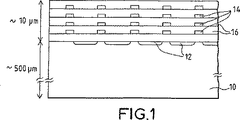
図1は、複数の画像センサの画像検出回路が従来技術を用いて作られたシリコンウェハの一般的な構造を示す。
シリコンウェハ10は、直径150ないし300ミリメートルの場合、数百マイクロメートルの厚さを有する。
画像検出回路(感光ドット、トランジスタ及び相互接続のマトリクス)がシリコンウェハの一面に加工され、この面は前面と呼ぶことができ、図1における上方面である。該加工とは、第一に、特に感光領域12を形成するためにウェハの上方面からシリコンに行われる様々な拡散及び注入作業を意味し、第二に、感光領域12の最表面にスタックを形成する導電層14及び絶縁層16の堆積及びエッチングのための連続的な作業を意味する。絶縁及び導電層は画像検出回路の一部をなし、センサに映された画像によって感光領域に生成される電荷の収集を可能にする。
導電層14の1つ、原則的には最後に堆積された層が、感光ドットのマトリクスを備える活性領域の周辺に各センサの入力/出力パッド(図1には該パッドは図示されていない)を形成する働きをする。
FIG. 1 shows the general structure of a silicon wafer in which the image detection circuits of a plurality of image sensors are made using conventional techniques.
The
An image detection circuit (photosensitive dots, transistors and interconnect matrix) is processed on one side of the silicon wafer, which can be referred to as the front side, which is the upper side in FIG. The processing means firstly various diffusion and implantation operations performed on the silicon from the upper surface of the wafer to form the
One of the conductive layers 14, in principle the last deposited layer, is an input / output pad for each sensor around the active area with a matrix of photosensitive dots (the pads are not shown in FIG. 1). Work to form.
センサが従来技術によって製造される場合、モザイク状のカラーフィルタはウェハ表面に堆積されることになる。
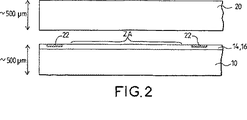
本発明では、この段階ではカラーフィルタは堆積されず、ウェハの前面が仮基板20(図2)に移載される。仮基板20は、製造中の構造の剛性を確保するためにウェハ10と同一の直径と類似の厚さを有するウェハである。また、別のシリコンウェハで構成されてもよい。移載は、絶縁及び導電層のスタックの堆積及びエッチング作業によってシリコンウェハの前面に形成された凹凸を埋める働きをする平坦化層を堆積させた後に行うことができる。該平坦化層は透過性である必要はない。
If the sensor is manufactured according to the prior art, a mosaic color filter will be deposited on the wafer surface.
In the present invention, the color filter is not deposited at this stage, and the front surface of the wafer is transferred to the temporary substrate 20 (FIG. 2). The
図2は、活性領域ZAと該領域ZA周辺の接続パッド22を備える独立したセンサの全体を示すために、図1よりも小さい尺度で構造を表したものである。導電層14と接触する又は層14の一部をなすパッド22は、2つのウェハ10及び20の間の接触面と同一平面上にあることが好ましい;平坦化層が堆積されている場合は、該層がパッド22を覆わないことを確実にすることが好ましい。しかし、パッドが平坦化層に覆われる場合、加工プロセスの最後に、これらパッドにアクセスするための孔をいずれにしても形成できることは後に説明する。
シリコンウェハの支持ウェハ20への移載は複数の手段で行うことができる。最も単純な手段は、接触する表面の平坦性が良好であると非常に強い接触力が生成されるので、分子レベルで密着させることによってウェハを保持するというものである。接着も可能である。
FIG. 2 shows the structure on a smaller scale than FIG. 1 in order to show the entire independent sensor including the active region ZA and the
The transfer of the silicon wafer onto the
シリコンウェハの前面が支持ウェハに移載された後、層のスタックの厚さを含めて約8ないし30マイクロメートルの厚さだけが残るように、シリコンウェハの厚さの大部分が除去される。シリコンウェハの残る部分は、数マイクロメートル(例えば5ないし10マイクロメートル)の層14、16のスタックの重畳と、約3ないし20マイクロメートルの、感光領域12を含む残りのシリコンの厚さだけである。該残りの厚さは、図1の感光領域12を含む図3の層30の厚さである。
薄化作業は、機械加工(ラッピング)を施し仕上げに化学加工することによって、又は機械/化学加工によって、又は化学加工のみによって、又はさらには薄化シリコン層の境界を定めることとなる平面に脆化不純物を予め注入することを必要とする特定の分離方法によって行うことができる。
不純物の注入によって分離する場合、注入はシリコンウェハを支持ウェハに移載する前に行わなくてはならない。実際に、注入はシリコンウェハの前面に、該ウェハの全表面にわたって、切り分け面を定義する深さで行われる。事前の注入は水素注入であることが好ましい。これは、ウェハ製造の様々な段階で行うことができるが、注入された切り分け面に沿ったウェハの厚さの分離は、シリコンウェハが支持ウェハに取り付けられた後にしか行えない。
After the front side of the silicon wafer is transferred to the support wafer, most of the thickness of the silicon wafer is removed so that only a thickness of about 8 to 30 micrometers, including the thickness of the stack of layers, remains. . The remaining portion of the silicon wafer is only a stack of several micrometer (eg, 5 to 10 micrometer) layers 14, 16 and the remaining silicon thickness, including the
The thinning operation can be performed by machining (wrapping) and chemically processing the finish, or by mechanical / chemical processing, or by chemical processing alone, or even on a plane that will delimit the thinned silicon layer. This can be done by a specific separation method that requires pre-implantation of phosphide impurities.
In the case of separation by impurity implantation, the implantation must be performed before the silicon wafer is transferred to the support wafer. In practice, the implantation is performed on the front side of the silicon wafer, at a depth that defines the cutting plane across the entire surface of the wafer. The pre-injection is preferably hydrogen injection. This can be done at various stages of wafer fabrication, but the separation of the wafer thickness along the implanted cut surface can only be done after the silicon wafer is attached to the support wafer.
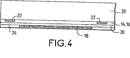
薄化されたシリコン層30の上方面を、表面の不具合を解消するために処理(ファインラッピング、化学洗浄、機械/化学研磨等)することができ、概略的な構造が図3の画像センサに係る断面図に示されるような形態を有するようになる。そして、モザイク状カラーフィルタ18は、層30(図4)の表面に堆積される。所望であれば、カラーフィルタの堆積前に、一つまたは複数の付加的な層、特に不動態化層、反射防止層および他の層、例えば堆積されたシリコン層の電気活性に必要な層(電気分極層)を堆積させることができる。
必要であれば、平坦化層24がモザイク状フィルタに堆積される。該層はフィルタを覆う場合透過性でなくてはならない。次に、カラーフィルタを支える仮基板20の前面が、最終の透過性基板40(ガラス又はプラスチック製)に移載される。該基板は、仮基板及び最初のシリコンウェハと同様の直径を有するウェハの形態である。最終基板の厚さは、加工中の構造の剛性を確保するために少なくとも数百マイクロメートルである(図5)。
仮基板の最終基板への移載は、接着(透過性の接着剤での)又は分子レベルで密着させることによってなされる。
The upper surface of the thinned
If necessary, a
The temporary substrate is transferred to the final substrate by adhesion (with a permeable adhesive) or adhesion at the molecular level.
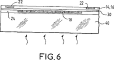
仮基板20の大部分又はさらには全体が、機械的及び/又は化学的手段、又は例えば上述したような水素注入による脆化によって除去される。この場合、基板20を部分的に除去するために、支持ウェハ20への水素注入は、シリコンウェハをウェハ20に最初に移載する前に行わなければならない。このことは、ウェハ20への移載と基板40への移載との間に、水素注入された平面で破損を引き起こす虞のある温度での作業は何ら実施されないことを意味する。
図6の場合、基板20は、接続パッド22が構造の表面と同一平面で重なるまで完全に除去されている。
図7の場合、基板20は部分的にのみ除去されている。わずかな厚さ(可能であれば最大数マイクロメートル)が残されており、該厚さには、接続パッド22へのアクセス領域を開放するために、化学腐食又は他の手段を用いて孔70が形成されることとなる。
Most or even the entire
In the case of FIG. 6, the
In the case of FIG. 7, the
図7の場合の接続パッドは「ワイヤボンディング」タイプのプリント回路基板との接続に使用されうる。光は透過性の最終基板40側から差し込まなければならないので、プリント回路基板は、感光活性領域と対向しているように面していなければならない。
図6の場合、接続パッド22は画像センサの上方面のレベルと同一平面で重なる。これらは、「ワイヤボンディング」又は「フリップチップ」タイプの接続(チップが、プリント回路基板の対応するパッドに対して該接続パッドと上下逆に配置される)に使用されうる。この場合、センサはプリント回路基板の上部から照射される。
接続パッド22が孔70内に押し込まれている図7のセンサでも同じくフリップチップタイプの組み立てを使用したい場合、以下の手順が行われることとなる:付加的な金属を堆積及びエッチングし、ここで該金属は孔70の底だけでなく、構造の外表面(つまり孔70が形成されている基板20の残りの部分の上方面)にも載せられる。構造の外部接続パッドはこうして孔70の外側に形成されることとなる。
The connection pads in the case of FIG. 7 can be used for connection to a “wire bonding” type printed circuit board. Since light must be inserted from the transmissive
In the case of FIG. 6, the
If the sensor of FIG. 7 with the
これら異なる実施形態において、基板40上に形成された構造は、接続パッドを用いてウェハ上で検査できる。該検査は、光の下、複数の画像パターン下、或いは他の条件下で実施できる。
構造は、加工プロセスの最後に、パッケージングのために各センサに切り分けられる。
カラーフィルタを支える薄化されたシリコン層に対して密接にあてがわれた最終基板は、フィルタとシリコンの双方を保護する。
In these different embodiments, the structure formed on the
The structure is carved into each sensor for packaging at the end of the fabrication process.
The final substrate, applied closely to the thinned silicon layer that supports the color filter, protects both the filter and the silicon.
Claims (5)
−ウェハ(10)の前面を仮の支持基板(20)の前面に対して移載することと、
−画像検出回路を備える薄い半導体層(30)を基板に残して、半導体ウェハの厚さの大部分を除去することと、
−薄化された半導体層上に、カラーフィルタ(18)を堆積させることと、
−該カラーフィルタの堆積後、仮基板の、カラーフィルタを支える側を、透過性の最終基板(40)に移載することと、
−半導体ウェハを保護する薄層を残して仮基板(20)を部分的に除去し、入力/出力パッド(22)にアクセスするための孔(70)を前記薄層に形成することと、
−最後に、基板を個々のセンサに切り分けること
からなる画像センサの製造方法。Forming on the front surface of the semiconductor wafer (10) a series of active areas (ZA) each comprising an image detection circuit and corresponding to each image sensor, wherein each active area is an input / output pad (22); -Transferring the front surface of the wafer (10) to the front surface of the temporary support substrate (20);
-Removing most of the thickness of the semiconductor wafer, leaving a thin semiconductor layer (30) with image detection circuitry on the substrate;
Depositing a color filter (18) on the thinned semiconductor layer;
-After depositing the color filter, transferring the side of the temporary substrate that supports the color filter to the transmissive final substrate (40);
-Partially removing the temporary substrate (20) leaving a thin layer protecting the semiconductor wafer and forming holes (70) in the thin layer for accessing the input / output pads (22);
-Finally, a method for manufacturing an image sensor, which comprises cutting the substrate into individual sensors.
Applications Claiming Priority (2)
| Application Number | Priority Date | Filing Date | Title |
|---|---|---|---|
| FR0111335A FR2829290B1 (en) | 2001-08-31 | 2001-08-31 | COLOR IMAGE SENSOR ON TRANSPARENT SUBSTRATE AND MANUFACTURING METHOD |
| PCT/FR2002/002977 WO2003019667A1 (en) | 2001-08-31 | 2002-08-30 | Colour image sensor on transparent substrate and method for making same |
Publications (3)
| Publication Number | Publication Date |
|---|---|
| JP2005501420A JP2005501420A (en) | 2005-01-13 |
| JP2005501420A5 JP2005501420A5 (en) | 2007-12-06 |
| JP4147187B2 true JP4147187B2 (en) | 2008-09-10 |
Family
ID=8866878
Family Applications (1)
| Application Number | Title | Priority Date | Filing Date |
|---|---|---|---|
| JP2003523013A Expired - Fee Related JP4147187B2 (en) | 2001-08-31 | 2002-08-30 | Manufacturing method of color image sensor on transparent substrate |
Country Status (10)
| Country | Link |
|---|---|
| US (1) | US6933585B2 (en) |
| EP (1) | EP1421622B1 (en) |
| JP (1) | JP4147187B2 (en) |
| KR (1) | KR100919964B1 (en) |
| CN (1) | CN100487899C (en) |
| CA (1) | CA2457899C (en) |
| DE (1) | DE60223263T2 (en) |
| FR (1) | FR2829290B1 (en) |
| IL (2) | IL160113A0 (en) |
| WO (1) | WO2003019667A1 (en) |
Families Citing this family (11)
| Publication number | Priority date | Publication date | Assignee | Title |
|---|---|---|---|---|
| FR2863773B1 (en) * | 2003-12-12 | 2006-05-19 | Atmel Grenoble Sa | PROCESS FOR THE PRODUCTION OF AMINCI SILICON ELECTRONIC CHIPS |
| KR100741920B1 (en) * | 2004-12-30 | 2007-07-24 | 동부일렉트로닉스 주식회사 | method for fabricating CMOS image sensor |
| JP4486043B2 (en) * | 2004-12-30 | 2010-06-23 | 東部エレクトロニクス株式会社 | CMOS image sensor and manufacturing method thereof |
| US8791006B2 (en) * | 2005-10-29 | 2014-07-29 | Stats Chippac, Ltd. | Semiconductor device and method of forming an inductor on polymer matrix composite substrate |
| US8158510B2 (en) | 2009-11-19 | 2012-04-17 | Stats Chippac, Ltd. | Semiconductor device and method of forming IPD on molded substrate |
| US8409970B2 (en) * | 2005-10-29 | 2013-04-02 | Stats Chippac, Ltd. | Semiconductor device and method of making integrated passive devices |
| DE102006014247B4 (en) * | 2006-03-28 | 2019-10-24 | Robert Bosch Gmbh | Image recording system and method for its production |
| US20090174018A1 (en) * | 2008-01-09 | 2009-07-09 | Micron Technology, Inc. | Construction methods for backside illuminated image sensors |
| JP5347520B2 (en) | 2009-01-20 | 2013-11-20 | ソニー株式会社 | Method for manufacturing solid-state imaging device |
| US8310021B2 (en) * | 2010-07-13 | 2012-11-13 | Honeywell International Inc. | Neutron detector with wafer-to-wafer bonding |
| US10985204B2 (en) * | 2016-02-16 | 2021-04-20 | G-Ray Switzerland Sa | Structures, systems and methods for electrical charge transport across bonded interfaces |
Family Cites Families (7)
| Publication number | Priority date | Publication date | Assignee | Title |
|---|---|---|---|---|
| US4758734A (en) * | 1984-03-13 | 1988-07-19 | Nec Corporation | High resolution image sensor array using amorphous photo-diodes |
| US4976802A (en) * | 1989-10-16 | 1990-12-11 | Xerox Corporation | Process for assembling smaller scanning or printing arrays together to form a longer array |
| JPH05183141A (en) * | 1991-07-12 | 1993-07-23 | Fuji Xerox Co Ltd | Color image sensor |
| US5244817A (en) * | 1992-08-03 | 1993-09-14 | Eastman Kodak Company | Method of making backside illuminated image sensors |
| US6059188A (en) * | 1993-10-25 | 2000-05-09 | Symbol Technologies | Packaged mirror including mirror travel stops |
| JPH0945886A (en) * | 1995-08-01 | 1997-02-14 | Sharp Corp | Amplifying semiconductor image pickup device |
| US6204087B1 (en) * | 1997-02-07 | 2001-03-20 | University Of Hawai'i | Fabrication of three-dimensional architecture for solid state radiation detectors |
-
2001
- 2001-08-31 FR FR0111335A patent/FR2829290B1/en not_active Expired - Fee Related
-
2002
- 2002-08-30 EP EP02796331A patent/EP1421622B1/en not_active Expired - Fee Related
- 2002-08-30 JP JP2003523013A patent/JP4147187B2/en not_active Expired - Fee Related
- 2002-08-30 CA CA2457899A patent/CA2457899C/en not_active Expired - Fee Related
- 2002-08-30 DE DE60223263T patent/DE60223263T2/en not_active Expired - Lifetime
- 2002-08-30 KR KR1020047001560A patent/KR100919964B1/en not_active IP Right Cessation
- 2002-08-30 IL IL16011302A patent/IL160113A0/en unknown
- 2002-08-30 US US10/485,694 patent/US6933585B2/en not_active Expired - Fee Related
- 2002-08-30 CN CNB028170423A patent/CN100487899C/en not_active Expired - Fee Related
- 2002-08-30 WO PCT/FR2002/002977 patent/WO2003019667A1/en active IP Right Grant
-
2004
- 2004-01-29 IL IL160113A patent/IL160113A/en not_active IP Right Cessation
Also Published As
| Publication number | Publication date |
|---|---|
| DE60223263D1 (en) | 2007-12-13 |
| IL160113A (en) | 2009-07-20 |
| FR2829290B1 (en) | 2004-09-17 |
| EP1421622A1 (en) | 2004-05-26 |
| FR2829290A1 (en) | 2003-03-07 |
| CN100487899C (en) | 2009-05-13 |
| CA2457899A1 (en) | 2003-03-06 |
| CN1550041A (en) | 2004-11-24 |
| DE60223263T2 (en) | 2008-08-14 |
| US6933585B2 (en) | 2005-08-23 |
| CA2457899C (en) | 2012-07-03 |
| WO2003019667A1 (en) | 2003-03-06 |
| EP1421622B1 (en) | 2007-10-31 |
| JP2005501420A (en) | 2005-01-13 |
| KR100919964B1 (en) | 2009-10-01 |
| IL160113A0 (en) | 2004-06-20 |
| US20040188792A1 (en) | 2004-09-30 |
| KR20040047783A (en) | 2004-06-05 |
Similar Documents
| Publication | Publication Date | Title |
|---|---|---|
| JP4064347B2 (en) | Color image sensor with improved colorimetry and manufacturing method thereof | |
| US6841454B2 (en) | Chip-like electronic components, a method of manufacturing the same, a pseudo wafer therefor and a method of manufacturing thereof | |
| US8501579B2 (en) | Process of fabricating chip | |
| TWI408790B (en) | Semiconductor device including through-electrode and method of manufacturing the same | |
| US20030151124A1 (en) | Integrated circuit device | |
| JP6147250B2 (en) | Imaging device manufacturing method and semiconductor device manufacturing method | |
| JP2000003889A (en) | Semiconductor wafer and manufacture of semiconductor | |
| KR20040110995A (en) | Method for manufacturing semiconductor device | |
| JP4147187B2 (en) | Manufacturing method of color image sensor on transparent substrate | |
| JP4180512B2 (en) | Method for manufacturing color image sensor in which contact hole is opened before thinning | |
| JP4733347B2 (en) | Method of manufacturing color image sensor having pad and support substrate to which pad is soldered | |
| JP4863214B2 (en) | Manufacturing method of electronic chip made of thinned silicon | |
| WO2021199679A1 (en) | Imaging element and method for manufacturing imaging element | |
| KR101287308B1 (en) | Thinned image sensor having trench-isolated contact pads | |
| US7705432B2 (en) | Three dimensional six surface conformal die coating | |
| TWI520312B (en) | Package process of backside illumination image sensor | |
| WO2021199695A1 (en) | Imaging element and method for manufacturing imaging element | |
| JP2674411B2 (en) | Method for manufacturing semiconductor device | |
| KR100513412B1 (en) | Semiconductor device equipped with a substrate bonded to the support | |
| JP2004165540A (en) | Semiconductor device and its manufacturing method | |
| JPS6324681A (en) | Manufacture of thin film of semiconductor element |
Legal Events
| Date | Code | Title | Description |
|---|---|---|---|
| A621 | Written request for application examination |
Free format text: JAPANESE INTERMEDIATE CODE: A621 Effective date: 20050816 |
|
| A977 | Report on retrieval |
Free format text: JAPANESE INTERMEDIATE CODE: A971007 Effective date: 20070425 |
|
| A131 | Notification of reasons for refusal |
Free format text: JAPANESE INTERMEDIATE CODE: A131 Effective date: 20070522 |
|
| A601 | Written request for extension of time |
Free format text: JAPANESE INTERMEDIATE CODE: A601 Effective date: 20070817 |
|
| A602 | Written permission of extension of time |
Free format text: JAPANESE INTERMEDIATE CODE: A602 Effective date: 20070824 |
|
| A601 | Written request for extension of time |
Free format text: JAPANESE INTERMEDIATE CODE: A601 Effective date: 20070919 |
|
| A524 | Written submission of copy of amendment under article 19 pct |
Free format text: JAPANESE INTERMEDIATE CODE: A524 Effective date: 20071003 |
|
| A602 | Written permission of extension of time |
Free format text: JAPANESE INTERMEDIATE CODE: A602 Effective date: 20071024 |
|
| A131 | Notification of reasons for refusal |
Free format text: JAPANESE INTERMEDIATE CODE: A131 Effective date: 20071211 |
|
| A601 | Written request for extension of time |
Free format text: JAPANESE INTERMEDIATE CODE: A601 Effective date: 20080311 |
|
| A602 | Written permission of extension of time |
Free format text: JAPANESE INTERMEDIATE CODE: A602 Effective date: 20080318 |
|
| A521 | Request for written amendment filed |
Free format text: JAPANESE INTERMEDIATE CODE: A523 Effective date: 20080411 |
|
| TRDD | Decision of grant or rejection written | ||
| A01 | Written decision to grant a patent or to grant a registration (utility model) |
Free format text: JAPANESE INTERMEDIATE CODE: A01 Effective date: 20080610 |
|
| A01 | Written decision to grant a patent or to grant a registration (utility model) |
Free format text: JAPANESE INTERMEDIATE CODE: A01 |
|
| A61 | First payment of annual fees (during grant procedure) |
Free format text: JAPANESE INTERMEDIATE CODE: A61 Effective date: 20080623 |
|
| R150 | Certificate of patent or registration of utility model |
Free format text: JAPANESE INTERMEDIATE CODE: R150 |
|
| FPAY | Renewal fee payment (event date is renewal date of database) |
Free format text: PAYMENT UNTIL: 20110627 Year of fee payment: 3 |
|
| FPAY | Renewal fee payment (event date is renewal date of database) |
Free format text: PAYMENT UNTIL: 20110627 Year of fee payment: 3 |
|
| FPAY | Renewal fee payment (event date is renewal date of database) |
Free format text: PAYMENT UNTIL: 20120627 Year of fee payment: 4 |
|
| FPAY | Renewal fee payment (event date is renewal date of database) |
Free format text: PAYMENT UNTIL: 20120627 Year of fee payment: 4 |
|
| FPAY | Renewal fee payment (event date is renewal date of database) |
Free format text: PAYMENT UNTIL: 20130627 Year of fee payment: 5 |
|
| LAPS | Cancellation because of no payment of annual fees |