JP4132546B2 - Light diffusing plate, method for manufacturing light diffusing plate, and display device - Google Patents
Light diffusing plate, method for manufacturing light diffusing plate, and display device Download PDFInfo
- Publication number
- JP4132546B2 JP4132546B2 JP2000053391A JP2000053391A JP4132546B2 JP 4132546 B2 JP4132546 B2 JP 4132546B2 JP 2000053391 A JP2000053391 A JP 2000053391A JP 2000053391 A JP2000053391 A JP 2000053391A JP 4132546 B2 JP4132546 B2 JP 4132546B2
- Authority
- JP
- Japan
- Prior art keywords
- light
- photosensitive
- sphere
- diffusing plate
- coloring material
- Prior art date
- Legal status (The legal status is an assumption and is not a legal conclusion. Google has not performed a legal analysis and makes no representation as to the accuracy of the status listed.)
- Expired - Fee Related
Links
- 238000004519 manufacturing process Methods 0.000 title claims description 29
- 238000000034 method Methods 0.000 title claims description 19
- 239000000463 material Substances 0.000 claims description 258
- 238000004040 coloring Methods 0.000 claims description 99
- 238000009792 diffusion process Methods 0.000 claims description 90
- 239000004973 liquid crystal related substance Substances 0.000 claims description 43
- 239000011230 binding agent Substances 0.000 claims description 41
- 239000000839 emulsion Substances 0.000 claims description 25
- 238000000149 argon plasma sintering Methods 0.000 claims description 19
- -1 silver halide Chemical class 0.000 claims description 16
- 230000002265 prevention Effects 0.000 claims description 15
- 229910052709 silver Inorganic materials 0.000 claims description 15
- 239000004332 silver Substances 0.000 claims description 15
- 239000011159 matrix material Substances 0.000 claims description 13
- 239000012954 diazonium Substances 0.000 claims description 12
- 150000001989 diazonium salts Chemical class 0.000 claims description 12
- 230000003287 optical effect Effects 0.000 claims description 10
- 239000003094 microcapsule Substances 0.000 claims description 8
- 239000002775 capsule Substances 0.000 claims description 5
- 238000005406 washing Methods 0.000 claims description 5
- 239000002243 precursor Substances 0.000 claims description 4
- 239000011358 absorbing material Substances 0.000 claims description 3
- AAAQKTZKLRYKHR-UHFFFAOYSA-N triphenylmethane Chemical compound C1=CC=CC=C1C(C=1C=CC=CC=1)C1=CC=CC=C1 AAAQKTZKLRYKHR-UHFFFAOYSA-N 0.000 claims description 3
- 239000011324 bead Substances 0.000 description 90
- 229920005989 resin Polymers 0.000 description 10
- 239000011347 resin Substances 0.000 description 10
- 238000002834 transmittance Methods 0.000 description 10
- 230000008569 process Effects 0.000 description 9
- 239000003086 colorant Substances 0.000 description 7
- 238000003745 diagnosis Methods 0.000 description 7
- 238000010586 diagram Methods 0.000 description 7
- 150000001875 compounds Chemical class 0.000 description 6
- 230000000694 effects Effects 0.000 description 5
- 230000031700 light absorption Effects 0.000 description 5
- 239000011248 coating agent Substances 0.000 description 4
- 238000000576 coating method Methods 0.000 description 4
- 125000000664 diazo group Chemical group [N-]=[N+]=[*] 0.000 description 4
- 238000010438 heat treatment Methods 0.000 description 4
- 239000006096 absorbing agent Substances 0.000 description 3
- 239000000203 mixture Substances 0.000 description 3
- 230000009467 reduction Effects 0.000 description 3
- OAZWDJGLIYNYMU-UHFFFAOYSA-N Leucocrystal Violet Chemical compound C1=CC(N(C)C)=CC=C1C(C=1C=CC(=CC=1)N(C)C)C1=CC=C(N(C)C)C=C1 OAZWDJGLIYNYMU-UHFFFAOYSA-N 0.000 description 2
- BQCADISMDOOEFD-UHFFFAOYSA-N Silver Chemical compound [Ag] BQCADISMDOOEFD-UHFFFAOYSA-N 0.000 description 2
- 230000009471 action Effects 0.000 description 2
- 239000000853 adhesive Substances 0.000 description 2
- 230000001070 adhesive effect Effects 0.000 description 2
- 239000000470 constituent Substances 0.000 description 2
- 238000005859 coupling reaction Methods 0.000 description 2
- 150000002148 esters Chemical class 0.000 description 2
- 239000003999 initiator Substances 0.000 description 2
- 239000000178 monomer Substances 0.000 description 2
- 229920000570 polyether Polymers 0.000 description 2
- 238000003825 pressing Methods 0.000 description 2
- 238000004062 sedimentation Methods 0.000 description 2
- 125000000391 vinyl group Chemical group [H]C([*])=C([H])[H] 0.000 description 2
- 229920002554 vinyl polymer Polymers 0.000 description 2
- 230000000007 visual effect Effects 0.000 description 2
- XLYOFNOQVPJJNP-UHFFFAOYSA-N water Substances O XLYOFNOQVPJJNP-UHFFFAOYSA-N 0.000 description 2
- BQCIDUSAKPWEOX-UHFFFAOYSA-N 1,1-Difluoroethene Chemical compound FC(F)=C BQCIDUSAKPWEOX-UHFFFAOYSA-N 0.000 description 1
- RNIPJYFZGXJSDD-UHFFFAOYSA-N 2,4,5-triphenyl-1h-imidazole Chemical class C1=CC=CC=C1C1=NC(C=2C=CC=CC=2)=C(C=2C=CC=CC=2)N1 RNIPJYFZGXJSDD-UHFFFAOYSA-N 0.000 description 1
- RSWGJHLUYNHPMX-UHFFFAOYSA-N Abietic-Saeure Natural products C12CCC(C(C)C)=CC2=CCC2C1(C)CCCC2(C)C(O)=O RSWGJHLUYNHPMX-UHFFFAOYSA-N 0.000 description 1
- 239000004925 Acrylic resin Substances 0.000 description 1
- 229920000178 Acrylic resin Polymers 0.000 description 1
- 108010010803 Gelatin Proteins 0.000 description 1
- 239000000020 Nitrocellulose Substances 0.000 description 1
- 229920002845 Poly(methacrylic acid) Chemical class 0.000 description 1
- 239000004952 Polyamide Substances 0.000 description 1
- 239000004721 Polyphenylene oxide Substances 0.000 description 1
- 239000004734 Polyphenylene sulfide Substances 0.000 description 1
- 239000004743 Polypropylene Substances 0.000 description 1
- 239000004793 Polystyrene Substances 0.000 description 1
- KHPCPRHQVVSZAH-HUOMCSJISA-N Rosin Natural products O(C/C=C/c1ccccc1)[C@H]1[C@H](O)[C@@H](O)[C@@H](O)[C@@H](CO)O1 KHPCPRHQVVSZAH-HUOMCSJISA-N 0.000 description 1
- XTXRWKRVRITETP-UHFFFAOYSA-N Vinyl acetate Chemical compound CC(=O)OC=C XTXRWKRVRITETP-UHFFFAOYSA-N 0.000 description 1
- BZHJMEDXRYGGRV-UHFFFAOYSA-N Vinyl chloride Chemical compound ClC=C BZHJMEDXRYGGRV-UHFFFAOYSA-N 0.000 description 1
- 238000002679 ablation Methods 0.000 description 1
- 239000002253 acid Substances 0.000 description 1
- 230000002238 attenuated effect Effects 0.000 description 1
- 230000005540 biological transmission Effects 0.000 description 1
- SKIMEKUYIQHJQV-UHFFFAOYSA-N bromomethylsulfonylbenzene Chemical compound BrCS(=O)(=O)C1=CC=CC=C1 SKIMEKUYIQHJQV-UHFFFAOYSA-N 0.000 description 1
- 239000006229 carbon black Substances 0.000 description 1
- 229920001577 copolymer Polymers 0.000 description 1
- 230000008878 coupling Effects 0.000 description 1
- 238000010168 coupling process Methods 0.000 description 1
- 238000004945 emulsification Methods 0.000 description 1
- 239000005038 ethylene vinyl acetate Substances 0.000 description 1
- 239000008273 gelatin Substances 0.000 description 1
- 229920000159 gelatin Polymers 0.000 description 1
- 235000019322 gelatine Nutrition 0.000 description 1
- 235000011852 gelatine desserts Nutrition 0.000 description 1
- 239000011521 glass Substances 0.000 description 1
- 230000007246 mechanism Effects 0.000 description 1
- 229920001220 nitrocellulos Polymers 0.000 description 1
- 239000002245 particle Substances 0.000 description 1
- CMCWWLVWPDLCRM-UHFFFAOYSA-N phenidone Chemical compound N1C(=O)CCN1C1=CC=CC=C1 CMCWWLVWPDLCRM-UHFFFAOYSA-N 0.000 description 1
- 229920001200 poly(ethylene-vinyl acetate) Polymers 0.000 description 1
- 229920003229 poly(methyl methacrylate) Polymers 0.000 description 1
- 229920002037 poly(vinyl butyral) polymer Polymers 0.000 description 1
- 229920002647 polyamide Polymers 0.000 description 1
- 229920000515 polycarbonate Polymers 0.000 description 1
- 239000004417 polycarbonate Substances 0.000 description 1
- 229920000728 polyester Polymers 0.000 description 1
- 229920001225 polyester resin Polymers 0.000 description 1
- 239000004645 polyester resin Substances 0.000 description 1
- 229920006149 polyester-amide block copolymer Polymers 0.000 description 1
- 229920013716 polyethylene resin Polymers 0.000 description 1
- 239000004926 polymethyl methacrylate Substances 0.000 description 1
- 229920000098 polyolefin Polymers 0.000 description 1
- 229920000069 polyphenylene sulfide Polymers 0.000 description 1
- 229920001155 polypropylene Polymers 0.000 description 1
- 229920002223 polystyrene Polymers 0.000 description 1
- 229920005990 polystyrene resin Polymers 0.000 description 1
- 229920000915 polyvinyl chloride Chemical class 0.000 description 1
- 230000035945 sensitivity Effects 0.000 description 1
- 239000010703 silicon Substances 0.000 description 1
- 229910052710 silicon Inorganic materials 0.000 description 1
- 239000002904 solvent Substances 0.000 description 1
- 229920001909 styrene-acrylic polymer Polymers 0.000 description 1
- 229920002803 thermoplastic polyurethane Polymers 0.000 description 1
- KHPCPRHQVVSZAH-UHFFFAOYSA-N trans-cinnamyl beta-D-glucopyranoside Natural products OC1C(O)C(O)C(CO)OC1OCC=CC1=CC=CC=C1 KHPCPRHQVVSZAH-UHFFFAOYSA-N 0.000 description 1
Images


Classifications
-
- G—PHYSICS
- G02—OPTICS
- G02B—OPTICAL ELEMENTS, SYSTEMS OR APPARATUS
- G02B5/00—Optical elements other than lenses
- G02B5/02—Diffusing elements; Afocal elements
- G02B5/0205—Diffusing elements; Afocal elements characterised by the diffusing properties
- G02B5/021—Diffusing elements; Afocal elements characterised by the diffusing properties the diffusion taking place at the element's surface, e.g. by means of surface roughening or microprismatic structures
- G02B5/0226—Diffusing elements; Afocal elements characterised by the diffusing properties the diffusion taking place at the element's surface, e.g. by means of surface roughening or microprismatic structures having particles on the surface
-
- G—PHYSICS
- G02—OPTICS
- G02B—OPTICAL ELEMENTS, SYSTEMS OR APPARATUS
- G02B5/00—Optical elements other than lenses
- G02B5/02—Diffusing elements; Afocal elements
- G02B5/0273—Diffusing elements; Afocal elements characterized by the use
- G02B5/0278—Diffusing elements; Afocal elements characterized by the use used in transmission
-
- G—PHYSICS
- G02—OPTICS
- G02F—OPTICAL DEVICES OR ARRANGEMENTS FOR THE CONTROL OF LIGHT BY MODIFICATION OF THE OPTICAL PROPERTIES OF THE MEDIA OF THE ELEMENTS INVOLVED THEREIN; NON-LINEAR OPTICS; FREQUENCY-CHANGING OF LIGHT; OPTICAL LOGIC ELEMENTS; OPTICAL ANALOGUE/DIGITAL CONVERTERS
- G02F1/00—Devices or arrangements for the control of the intensity, colour, phase, polarisation or direction of light arriving from an independent light source, e.g. switching, gating or modulating; Non-linear optics
- G02F1/01—Devices or arrangements for the control of the intensity, colour, phase, polarisation or direction of light arriving from an independent light source, e.g. switching, gating or modulating; Non-linear optics for the control of the intensity, phase, polarisation or colour
- G02F1/13—Devices or arrangements for the control of the intensity, colour, phase, polarisation or direction of light arriving from an independent light source, e.g. switching, gating or modulating; Non-linear optics for the control of the intensity, phase, polarisation or colour based on liquid crystals, e.g. single liquid crystal display cells
- G02F1/133—Constructional arrangements; Operation of liquid crystal cells; Circuit arrangements
- G02F1/1333—Constructional arrangements; Manufacturing methods
- G02F1/1335—Structural association of cells with optical devices, e.g. polarisers or reflectors
- G02F1/133504—Diffusing, scattering, diffracting elements
Landscapes
- Physics & Mathematics (AREA)
- General Physics & Mathematics (AREA)
- Optics & Photonics (AREA)
- Nonlinear Science (AREA)
- Mathematical Physics (AREA)
- Crystallography & Structural Chemistry (AREA)
- Chemical & Material Sciences (AREA)
- Optical Elements Other Than Lenses (AREA)
- Liquid Crystal (AREA)
- Materials For Photolithography (AREA)
- Non-Silver Salt Photosensitive Materials And Non-Silver Salt Photography (AREA)
- Photosensitive Polymer And Photoresist Processing (AREA)
- Heat Sensitive Colour Forming Recording (AREA)
Description
【0001】
【発明の属する技術分野】
本発明は、光拡散板、光拡散板の製造方法および表示装置の技術分野に属し、詳しくは、広視野角を有し、かつ、高コントラストな画像を表示する液晶ディスプレイを実現できる光拡散板、このような光拡散板を製造する光拡散板の製造方法およびこれらの光拡散板を利用する液晶ディスプレイ表示装置やマトリクス構造を有する画像表示装置などの表示装置に関する。
【0002】
【従来の技術】
近年、ワードプロセッサやパーソナルコンピュータ等の普及に伴い、さまざまな画像表示装置が開発され、画像を表示するために用いられている。
画像表示装置は、一般に、画像情報電気信号を画像光に変換して表示画面に表示する表示デバイスと、この表示デバイスを駆動する駆動回路と、この駆動回路に電力を供給する電源とから構成される。表示の光学的方式や表示デバイスの駆動方式により、いろいろな画像表示装置があるが、従来、最も普及しているのはCRT(Cathode Ray Tube) ディスプレイである。例えば、超音波診断、CT診断、MRI診断等の医療分野においては、白黒CRTディスプレイが用いられるが、この白黒CRTディスプレイは、デジタル的なマトリクス構造がないため、なめらかで自然な画像を得ることができる。
【0003】
これに対して、最近は、小型化が容易で、薄く、軽量である等の利点から液晶ディスプレイ(Liquid Crystal Display、以下、LCDという)がさまざまな分野で用いられるようになって来ている。特に、ワードプロセッサやコンピュータのディスプレイとして、LCDの使用頻度が大幅に増大している。また、LCDは、超音波診断装置、CT診断装置、MRI診断装置等の、従来は、CRTが主流であった医療用診断装置のモニタとしても利用が検討されている。
【0004】
【発明が解決しようとする課題】
LCDは、上述したように、小型化が容易である、薄い、軽量である等、非常に多くの利点を有する反面、視野角特性が悪く(視野角が狭く)、すなわち見る方向や角度によって画像のコントラスト比が急激に低下してしまい、また階調の反転も生じ、画像の見え方が異なる。そのため、観察者の位置等によっては、画像を適正に観察することができないという問題点が有る。
特に、前述のような医療用の用途では、画像の濃淡で診断を行うので、コントラスト比の高い画像が要求される上に、画像の非適正な認識は誤診や診断結果の食い違い等の原因となる。そのため、特に、広い視野角にわたってコントラスト比の高い画像が要求される。さらに、医療用のモニタでは、表示画像は、通常はモノクロ画像であるため、視野角に依存する画像コントラストの低下が激しく、より問題となる。
【0005】
また、広視野角のLCDとして、IPS(In-Plane Swiching) モード、MVA(Multi-domain Vertical Alignement)モード等のLCDも知られてはいるが、これらでも、モノクロ画像、特に医療用の用途に対して、十分に広い視野角を確保するには至っていない。
他方、広い視野角に渡って良好なコントラスト比の画像を得ることができるLCDとして、バックライトとしてコリメート光(直進光)を用い(コリメートバックライト)、さらに、液晶パネルを通過した光を、拡散板で拡散させる方法が知られている。
しかしながら、拡散板を用いて、医療用途でも十分な視野角を実現したLCDは、今だ実現されてはいない。また、拡散板を用いる方法では、拡散板に入射する外光も反射、散乱されてしまい、これによって観察画像のコントラストが低下して、やはり、好適な画像の観察を行うことができない場合も多い。
【0006】
一方、LCDのように、デジタル画素のマトリクス構造が明瞭で、シャープネスが高く、高精細なディスプレイは、CG(Computer Graphics) のような人工的な画像の表示に適している。
しかしながら、LCDはデジタル画素のマトリクス構造を有しているため、例えば、X線画像のような自然ななめらかさを持つ静止画像に対しては、このマトリクス構造の明瞭さが、逆にモザイク感を与えてしまい、画像がギザギザするいわゆるピクセリゼーション(あるいはジャギー)という好ましくない状態が発生するという問題がある。これは画素サイズが大きい時(例えば、15″XGA (Extended Graphics Array)で画素サイズが300μm程度)に、カラーフィルタのマトリクス構造の縦の筋がはっきり見えて、特に顕著である。
また、LCDに限らず、カラーCRTやPDP(Plasma Display Panel) 等でも、マトリクス構造を有するものは、同様に、上記ピクセリゼーションが発生するという問題がある。
【0007】
本発明の第1の課題は、上記従来技術の問題点を解消し、優れた光拡散性能を有し、かつ、表面反射によるコントラスト低下も好適に低減して、液晶ディスプレイに利用することにより、広い視野角に渡って良好なコントラスト比を有し、医療用の用途にも好適な液晶ディスプレイを実現できるより耐光性の高い光拡散板および光拡散板の製造方法を提供することにある。
本発明の第2の課題は、上記従来技術の問題点を解消し、上記光拡散板を利用する液晶ディスプレイ表示装置、特に、ピクセリゼーション(ジャギー)をなくし(すなわち、デピクセリゼーションし)、なめらかで自然な表示画像を得ることのできる表示装置を提供することにある。
【0008】
【課題を解決するための手段】
上記第1の課題を達成するために、本発明の第1の態様の光拡散板の製造方法は、光透過性の支持体と、拡散層を形成する光透過性の球体と、前記支持体および前記球体の間に介在する感光性発色材料とを有する光拡散板を製造するに際し、
この感光性発色材料は、少なくともジアゾニウム塩、カプラーおよび塩基を含み、現像後に、非露光部が発色し、露光部が非発色となるものであり、前記拡散層側から前記球体および前記感光性発色材料に略平行光を入射し、前記球体によって集光された光によって前記感光性発色材料を露光した後に、前記感光性発色材料を加熱現像して、前記感光性発色材料の非露光部を発色させ、露光部を非発色とさせることを特徴とする。
ここで、前記ジアゾニウム塩、前記カプラーおよび前記塩基の少なくとも一種が、マイクロカプセルに包含されているのが好ましい。
【0009】
また、前記感光性発色材料は、前記支持体および拡散層の間において感光性発色材料層を形成するのが好ましい。
また、前記感光性発色材料は、前記球体に接触する材料であるのが好ましい。
また、本発明の光拡散板の製造方法は、上記各光拡散板の製造方法であって、前記光拡散板は、さらに、前記球体に接触する材料を有し、前記感光性発色材料は、前記球体に接触する材料と前記支持体との間に配されていることを特徴とする。
また、前記球体に接触する材料は、光吸収材料を含有しているのが好ましい。
また、前記拡散層は、前記球体に接触する材料の層を先に形成した後に、前記球体を埋め込むことにより形成されるのが好ましい。
また、前記支持体の前記拡散層と逆側の面が、光非反射処理を施されているのが好ましい。
また、前記発色領域(光非通過領域)の作用によって、外光に対する反射率が10%以下であるのが好ましい。
【0010】
また、上記第1の課題を達成するために、本発明の第1の態様の光拡散板は、光透過性の支持体と、拡散層を形成する光透過性の球体と、前記球体に接触する材料と、前記球体に接触する材料と前記支持体との間に配される第1感光性発色材料とを有し、前記第1感光性発色材料は、少なくともジアゾニウム塩、カプラーおよび塩基を含み、現像後に、非露光部が発色し、露光部が非発色となり、前記球体に接触する材料は、現像後に、露光部が発色する第2感光性発色材料であり、前記拡散層側から前記球体および前記第1および前記第2感光性発色材料に略平行光を入射し、入射した略平行光によって前記第2感光性発色材料を露光するとともに、前記球体に入射して前記球体によって集光された光によって前記第1感光性発色材料を露光した後に、前記第1および前記第2感光性発色材料を現像して、前記第2感光性発色材料の露光部および前記第1感光性発色材料の非露光部を発色させ、前記第1感光性発色材料の露光部を非発色とさせてなるものであり、前記第1感光性発色材料の現像は、加熱現像であることを特徴とする。
ここで、前記ジアゾニウム塩、前記カプラーおよび前記塩基の少なくとも一種がマイクロカプセルに包含されているのが好ましい。
【0011】
また、前記第2感光性発色材料は、ネガ型ハロゲン化銀感光乳剤であり、その現像は、写真乳剤用現像、定着および水洗処理であるのが好ましい。
または、前記第2感光性発色材料は、トリフェニルメタン系ロイコ染料前駆体と光酸発生剤と光ラジカル発生剤とラジカルクエンチャーとを含むネガ型感光性熱現像材料であるのが好ましい。
また、前記第1感光性発色材料は、光吸収材料を含有しているのが好ましい。
また、前記拡散層は、前記球体に接触する材料の層を先に形成した後に、前記球体を埋め込むことにより形成されたものであるのが好ましい。
また、前記支持体の前記拡散層と逆側の面が、光非反射処理を施されているのが好ましい。
【0012】
また、本発明の光拡散板は 光透過性の支持体と、拡散層を形成する光透過性の球体と、前記球体に接触する材料と、前記球体に接触する材料と前記支持体との間に配される第1感光性発色材料とを有し、前記第1感光性発色材料は、現像後に、非露光部が発色し、露光部が非発色となり、前記球体に接触する材料は、現像後に、露光部が発色する第2感光性発色材料であり、前記拡散層側から前記球体および前記第1および前記第2感光性発色材料に略平行光を入射し、入射した略平行光によって前記第2感光性発色材料を露光するとともに、前記球体に入射して前記球体によって集光された光によって前記第1感光性発色材料を露光した後に、前記第1および前記第2感光性発色材料を現像して、前記第2感光性発色材料の露光部および前記第1感光性発色材料の非露光部を発色させ、前記第1感光性発色材料の露光部を非発色とさせてなるものであり、前記支持体の前記拡散層と逆側の面が、光非反射処理を施されていることを特徴とする。
【0013】
また、上記第2の課題を解決するために、本発明の第2の態様の表示装置は、液晶ディスプレイパネルと、前記液晶ディスプレイパネルに平行光を入射するバックライト部と、前記液晶ディスプレイパネルに対して前記バックライト部と逆側に配置される上記第1の態様の光拡散板の製造方法によって製造された光拡散板または上記第1の態様の光拡散板とを有することを特徴とする。
ここで、前記光拡散板は、光学的な屈折力を持つ視認不可能な構造を有し、マトリクス構造を有する画像表示デバイスの表示画面の観察側に配設されるのが好ましい。
また、前記拡散層は、前記光透過性の球体をバインダに固定してなるのが好ましい。
また、前記表示画面の観察側に配設された光拡散板の上に、さらに外光散乱防止シートを配設するのが好ましい。
【0014】
【発明の実施の形態】
本発明に係る光拡散板、光拡散板の製造方法および表示装置を添付の図面に示す好適実施例に基づいて以下に詳細に説明する。
【0015】
図1に、本発明の第1の態様の光拡散板を利用する、本発明の第2の態様の表示装置の一実施例を概念的に示す。
図1に示される表示装置10は、画像の表示手段として液晶パネル12を利用する、いわゆる液晶ディスプレイ(以下、LCDとする)であって、液晶パネル12と、液晶パネル12にコリメート光(直進光)を入射させるバックライト部14と、液晶パネル12を通過した画像を担持する光を拡散する、本発明の第1の態様の光拡散板16とを有する。また、液晶パネル12には、これを駆動するドライバ(図示省略)が接続され、さらに、表示装置10には、公知のLCDが有する各種の部材が、必要に応じて配置される。
本発明の第1の態様の光拡散板16を利用する本発明の表示装置10は、広い視野角に渡って、高いコントラスト比を実現できるので、医療用診断装置のモニタ等に好適に利用可能である。
【0016】
本発明の表示装置10に利用される液晶パネル12には、特に限定はなく、所定の間隙を持って配置される透明な支持体の間に液晶を充填して、透明電極を配し、このシート状の液晶挟持支持体の一面に検光板を、他面に偏光板を配置してなる、各種のLCDに用いられる公知の液晶パネルが全て利用可能である。
従って、本発明の表示装置10に用いられる液晶パネル12は、カラーでもモノクロでもよく、また、動作モードも、TN(Twisted Nematic) モード、STN(Super Twisted Nematic) モード、ECB(Electrically Controlled Birefringence) モード、IPS(In Plane Switching) モード、MVA(Multidomain Vertical Alignment)モード等の全ての動作モードが利用可能である。中でも特に、TNモードの液晶パネルは好適である。TNモードの液晶表示は、視野角特性が低いものの、IPSモードやMVAモード等の広視野角なモードに比べ、液晶パネルそのものの構成が簡単である。そのため、高分解能とした際のバックライトの利用効率が高く、高精細な画像表示を容易に行うことができる。さらに、スイッチング素子やマトリクスにも特に限定はない。
【0017】
バックライト部14も、画像の観察に十分な光量のコリメート光を射出可能なものであれば、各種の光源装置が全て利用可能である。一例として、散乱光の一部の光のみを通過させるルーバを利用するもの、オーバーヘッドプロジェクタのように、点光源からの発光光をレンズによって平行にしたもの、マイクロレンズ効果を利用して散乱光から指向性を持つ平行光をつくり出すもの、等が好適に例示される。
【0018】
本発明の光拡散板16は、光学的な屈折力(光学的なパワー)を有し、かつ、表示装置10の観察者が視認することができない微細な球形等の構造を有し、かつ、この構造側から入射する平行光が主に通過する領域(通過領域)に比して、それ以外の領域(非通過領域)の方が、相対的に低い光透過性を有し、好ましくは、非通過領域が光吸収性を有する(ブラックマスクとなっている)。ここで、通過領域の材料と非通過領域の材料とが同時に塗布されたものであることが必要である。
また、この非通過領域の作用によって、外光に対する反射率が10%以下であるのが好ましい。
【0019】
図2(A)に、本発明の第1の態様の光拡散板の一実施例の概念的断面模式図を示す。
同図に示される光拡散板16aは、本発明の光拡散板16の実施例の1つであって、光透過性の支持シート18に、拡散層を構成する光透過性の球体(以下、ビーズとする)20を、露光部が非発色となる感光性発色材料(の層)24によって固定してなる構造を有する。また、ビーズ20は、その一部が支持シート18に接触している。ビーズ20の下部およびその近傍の感光性発色材料24は、予め、ビーズ20の側からのコリメート光により露光されて透明化し、一方、このコリメート光の非通過領域は、その後の現像処理により、発色している。
【0020】
従って、図2(A)に一点鎖線で示されるように、バックライト部14から射出され、液晶パネル12を通過した、画像を担持するコリメート光は、球形のビーズ20によって屈折(拡散)されて、光の通過領域となるビーズ20と支持シート18との接触部およびその近傍(以下、単に接触部という)を通過して、十分に拡散される。しかも、感光性発色材料(以下、発色材という)24の未露光部は、発色現像により光吸収性を有するので、ビーズ20と支持シート18との接触部以外の非通過領域はブラックマスクとなり、観察者側からの外光が光拡散板16によって反射、散乱されることがなく、これによるコントラストの低下もない。
そのため、本発明によれば、広い視野角に渡って良好なコントラスト比を得られる表示装置10(LCD)が実現できる。
【0021】
支持シート18には特に限定はなく、十分な光透過性を有し、かつ、用途に応じた十分な機械的強度を有するものであれば、各種の材料が利用可能である。
具体的には、各種のガラス、ポリエステル、ポリオレフィン、ポリアミド、ポリエーテル、ポリスチレン、ポリエステルアミド、ポリカーボネート、ポリフェニレンスルフィド、ポリエーテルエステル、ポリ塩化ビニル、ポリメタクリル酸エステルなどの各種の樹脂材料が好適に例示される。
なお、図示例の光拡散板16aを初めとして、本発明の光拡散板16は、剛性を有する板状であってもよく、可撓性を有するシート状あるいはフィルム状であってもよいので、要求される機械的強度や用途によって、支持シート18の材料や厚さ等を選択してもよい。
【0022】
また、表示装置10の観察性をより良好にするために、支持シート18の観察面(ビーズ20と逆側の面)には、AR(Anti Reflection) コート等の公知の光非反射処理を施すことにより、光非反射処理層23を設けておくのが好ましい。
【0023】
ビーズ20は、拡散層を形成するものであって、光透過性で、かつ観察者が視認できないサイズの(略)球体で、一部を支持シート18に接触した状態または近接した状態で、感光性発色材料(発色材)24によって支持シート18に固定される。
本発明の光拡散板16aにおいて、ビーズ20は前述の光学的な屈折率を有する構造を主に構成するものである。従って、ビーズ20を用いる光拡散板16a等は、ビーズ20側を液晶パネル12に向けて配置、保持される。
【0024】
ビーズ20の材料には特に限定はなく、透明であれば各種の材料が利用可能であり、例えば、前述の支持シート18の材料が各種例示され、特に光学特性が良好である等の点で、(メタ)アクリル系の樹脂やガラスが好適に利用される。
また、ビーズ20のサイズにも特に限定はなく、表示装置10の用途等に応じて、観察者が視認できないサイズであればよいが、好ましくは、重量平均粒子径で、3μm〜40μmであるのが好ましく、より好ましくは、5μm〜20μmであるのがよい。なお、後述する本発明の第2の態様の画像表示装置の光拡散板のビーズとして用いる場合には、より好ましいビーズのサイズは10μm〜21μmであるのが良い。
【0025】
感光性発色材料24は、ポジ型感光性発色材料(発色材)であって、露光によって露光部が非発色となり、その後、熱や現像処理によって現像され、非露光部が発色し、光遮蔽部(光の非通過領域)となり、非発色露光部が光透過部(光の通過領域)となる材料である。
【0026】
なお、本出願人は、特願2000−009136号明細書にて、このようなポジ型発色材の好ましい一例として、電子供与性の無色染料を内包する熱応答性マイクロカプセル、同一分子内に電子受容部と重合性ビニルモノマー部とを有する化合物、および光重合開始剤を含む発色材等を例示している。なお、この発色材においては、これらの化合物および光重合開始剤は、熱応答性マイクロカプセルの外に存在する。
この発色材は、露光された部分は、熱応答性マイクロカプセルの外の組成物(硬化性組成物とする)が硬化(重合)して固定化され、その後の加熱によっても化合物は移動しないが、未露光部は、加熱によって、移動性を有する(固定化されていない)前述の電子受容部と重合性ビニルモノマー部とを有する化合物もしくは電子受容性化合物が発色材内を移動して、マイクロカプセル内の電子供与性の無色染料を発色させて、ポジ画像を形成する記録材料である。
この発色材は、特開平10−226174号公報に詳述されている。
【0027】
また、これ以外にも、ポジ型感光性材料であれば、特開平3−87827号や同4−211252号公報に開示される発色材(感光性熱現像記録材料)も好適に利用可能である。
本出願人は、特願2000−009136号明細書において、光拡散板に適用可能なポジ型発色材として以上のようなポジ型感光性材料を開示しているが、本発明は、このようなポジ型感光性材料を用いた光拡散板よりもさらに耐光性の高い光拡散板16を提供するものである。
【0028】
このように耐光性の高い本発明の光拡散板16に用いることのできる感光性発色材料24としては、以下のようなものを挙げることができる。
すなわち、本発明に用いられる感光性発色材料24の好ましい一例としては、露光部が非発色となる感光性発色材料が少なくともジアゾニウム塩とカプラーと塩基とを含み、未露光部を発色現像する現像手段が加熱であるポジ型ジアゾ感光感熱材料(感光性熱現像材料)を挙げることができる。
この感光性発色材料の好ましい形態としては、油溶性のジアゾニウム塩がマイクロカプセル中に包含され、カプラーと塩基がその他の増感剤などと共に乳化分散された形でカプセルの外側に配されたものである。露光された部分では、ジアゾニウム塩は、カップリング機能を失って発色しないのに対し、未露光部では、加熱により溶融したカプラー、塩基、増感剤がカプセル内に進入しジアゾニウム塩とカップリング反応を起こして発色する。
この発色材は、特開平4−261893号に詳述されている。
【0029】
また、別の好ましい一例としては、露光部が非発色となる感光性発色材料がポジ型ハロゲン化銀感光乳剤であり、未露光部を発色現像する現像手段が写真用の現像、定着および水洗処理であることを特徴とする感光性材料が挙げられる。
このポジ型ハロゲン化銀感光乳剤の好ましい例としては、マイクロデュープフィルム用直接反転乳剤やレントゲンデュープ用直接反転乳剤等が挙げられる。
通常のネガ型ハロゲン化銀感光乳剤においては、露光部に感光核が発生し、これが現像により、金属銀へと還元されて黒色画像を形成するが、このポジ型感光乳剤では、ハロゲン化銀は、あらかじめかぶらせておき、これに減感色素を加えておくと露光部が還元されず、非露光部が還元されて発色銀を形成する。
これらのポジ型直接反転乳剤については、例えば丸善書店発行の「科学写真便覧」に記載されている。
これらのポジ型ハロゲン化銀感光乳剤の現像、定着および水洗処理には、通常の白黒乳剤用の処理液が好適に用いられる。
【0030】
このような光拡散板16aの作製方法には特に限定はないが、例えば、感光性発色材料24にビーズ20を分散して塗料を調製し、この塗料を支持シート18に塗布して乾燥(硬化)してもよく、あるいは、感光性発色材料24を支持シート18に塗布し、その上にビーズ20を全面的に散布して、その後、感光性発色材料24を乾燥してもよい。
【0031】
図2(B)に、本発明の光拡散板の別の実施例の概念的断面模式図を示す。
同図に示される光拡散板16bは、露光部が非発色の、すなわちポジ型の感光性材料として、上述したポジ型ジアゾ感光感熱材料やポジ型ハロゲン化銀感光乳剤などのポジ型の感光性発色材料24を用いて、感光性材料層(感光性発色材料層)24を形成し、その上に透明なバインダ25でビーズ20を固定した後、露光現像して、ブラックマスクを形成する。
なお、図2(B)に示される光拡散板16bは、多くの構成要素が図2(A)に示される光拡散板16aと同一であるので、同一の構成要素には同じ符号を付し、以下の説明は、異なる部位を主に行う。
【0032】
図2(B)に示される光拡散板16bは、支持シート18の上に、黒色に発色した感光性材料層、例えば感光性発色材料層(発色材層)24を有し、発色材層24の上に、ビーズ20が固定されており、かつ、発色材層24は、バインダ25によって固定されたビーズ20によって屈折された光が通過する領域(通過領域)では、発色していない。
従って、この光拡散板16bによっても、先の図2(A)示される実施例と同様に、液晶パネル12を通過した画像が担持されたコリメート光は、ビーズ20によって屈折されて、発色材層24の非発色部(光の通過領域)を通過して、好適に拡散されると共に、発色材層24がブラックマスク(光の非通過領域)となるので、外光の反射・散乱によるコントラストの低下もなく、広い視野角に渡って良好なコントラスト比を得られる表示装置10(LCD)が実現できる。
【0033】
このような光拡散板16bは、以下のようにして作製することができる。
まず、支持シート18に、上述した発色材24を必要に応じて水または溶媒に溶解もしくは分散して、塗布し、乾燥させて、発色材層24を形成する。
次いで、発色材層24の上に、ビーズ20を固定する。例えば、ビーズ20をバインダ25に分散した塗料を塗布し、あるいはバインダ25を塗布した後、ビーズ20を全面的に散布し、バインダ25を乾燥して、ビーズ20を固定する。なお、ビーズ20の固定に先立ち、バインダ25上のビーズ20の押圧や沈降によってビーズ20と発色材層24とを接触させてもよい。
【0034】
ビーズ20を固定したら、ビーズ20側からコリメート光、好ましくは、バックライト部14が射出するのと同様のコリメート光を入射する。これにより、ビーズ20に入射した光が屈折されて、(加えて、ビーズ20に入射しない光も)発色材層24に入射し、その領域(の発色材24)が露光される。すなわち、発色材層24における光が通過する領域のみが露光され、現像されても発色しない光の通過領域となる。
なお、ビーズ20と発色材層24などとの接触領域およびその近傍領域からなる光通過(透過)領域が露光され、光非通過(遮蔽)領域を構成する、光通過領域以外の領域は露光されないが、これは、ビーズ20に入射した光は、ビーズ20によって光通過領域に集光されるので、光通過領域にある発色材層24を露光できるが、光非通過領域に入射する光は、ビーズ20によって集光されていないために、光非通過領域にある発色材層24を良く露光できないからである。
【0035】
次いで、発色材層(の発色材)24を熱や写真乳剤用現像処理液によって現像することにより、未露光部分のみが発色して、光の非通過領域となり、露光部は光の通過領域となる。この現像で発色するのは、前述のように、ビーズ20によって屈折された光すなわち拡散光等が通過しない領域のみである。従って、発色材層24は、観察者側からの外光を吸収するブラックマスクとして、好適に作用する。
【0036】
本態様においては、ビーズ20の固定にバインダ25を用いる場合には、バインダ25は、光透過性を有するもの、特に無色透明であるのが好ましく、ビーズ20を支持シート18に固定できるものであれば、各種の接着剤が利用可能であり、例えば酢酸ビニル樹脂、エチレン−酢酸ビニル共重合体、塩化ビニル樹脂、塩化ビニル−塩化ビニリデン共重合体、(メタ)アクリル酸エステル樹脂、ブチラール樹脂、シリコン樹脂、ポリエステル樹脂、フッ化ビニリデン樹脂、ニトロセルロース樹脂、ポリスチレン樹脂、スチレン−アクリル共重合体、ウレタン樹脂、ポリエチレン樹脂、ポリプロピレン樹脂、塩化ポリエチレン樹脂、ロジン誘導体、ゼラチンおよびこれらの混合物が好適に例示される。
【0037】
また、特に限定されるわけではないが、ビーズ20の固定にバインダ25を用いる場合には、ビーズ20とバインダ25は屈折率の差が小さいのが好ましく、特に屈折率の差が0.1以下であるのが好ましい。これにより、両者の界面での光反射を防止することができ、より好適な画像の観察が可能となる。
さらに、本態様においては、バインダ25とビーズ20の量比にも特に限定はないが、重量比で1〜5とするのが、表面状態や画像表示時の光拡散板表面の輝度等の点で好ましい。なお、本態様において、バインダ25は光透過性であるので、ビーズ20はバインダ25に埋没してもよい。
【0038】
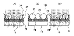
ところで、図3(A)および図4(A)に示すように、比較的高感度のポジ型感光性材料でブラックマスクとなる発色材層24をセルフアラインメントプロセスで形成する場合、ビーズ20とビーズ20との間隙の部分にも光が照射されて露光されるので、現像後に光を透過するようになる。これは、発色材24がブラックマスクとならず、図3(B)および図4(B)に示す拡散板16cや16dがブラックスクリーンとして期待する機能を損なうので、この部分は光を透過しなくなるような対策が必要である。
【0039】
このため、図3(B)に示す拡散板16cや図4(B)に示す拡散板16dを製造する際には、発色材層(感光性材料層)24自体またはその上層(露光光源に近い層)、例えばバインダ30を、露光光を中程度に吸収する層、すなわち露光光に対して中程度の濃度を持つ層として形成する。発色材層24自体、またはその上層のバインダ30を、このような中程度の濃度を持つ層として形成するには、発色材層24を形成する材料自体またはその上層のバインダ30自体が中程度の濃度を持つものを用いても良いが、発色材層24またはその上層のバインダ30に、露光光を中程度に吸収する光吸収剤を添加しても良い。
なお、このようなバインダ30の材料としては、バインダ25に用いられる材料を用いることができるが、バインダ25のように無色透明にする必要はなく、材料自体が無色透明である場合や材料自体では露光光の吸収が少ない場合には、露光光を中程度に吸収するように所要量のカーボンブラック等の光吸収剤を添加して光吸収性を付与したものでも良い。
【0040】
これによって、ビーズ20間の間隙部分(例えば、図3(A)に示す発色材層24や図4(A)に示すバインダ30)は、中程度の濃度を持ち、層厚が厚いので露光光は減衰して、発色材層24の感光性材料を十分露光せず、現像後に発色して可視光を遮蔽するようになる。一方、ビーズ20を透過する光は、光吸収層である図3(A)に示す発色材層24や図4(A)に示すバインダ30が薄いので、その光路にある発色材層24の感光性材料は露光されて現像後に発色せず、また、光吸収層が薄いから、所期の機能である光透過性を損なわない。
【0041】
従って、図3(B)に示すような拡散板16cを製造する場合には、透明な支持シート18にビーズ20を接着させるバインダーとして、その感光波長において中程度に濃度を有し、熱や現像処理による現像した後に可視光域で高濃度に発色する感光性材料を用いる。
例えば、まず、透明な支持シート18上にこのような特性を持つ感光性材料からなる発色材層24を塗布し、その上にビーズ20を全面的に散布し、必要に応じてビーズ20を押圧や沈降によって支持シート18と接触させた後、発色材層24を乾燥して、発色材層24によってビーズ20を支持シート18に接着して固定する。
【0042】
この後、図3(A)に示すように、ビーズ20側から露光光としてコリメート光を入射すると、ビーズ20に入射した光が屈折されて、ビーズ20の底部と支持シート18との間、または両者の接触部近傍の薄い発色材層24の領域に入射する。この領域の発色材層24も、中程度の濃度を持つが、薄いので、十分に露光光が照射され、その領域が十分に露光される。この時、露光光は、ビーズ20間の間隙部分の発色材層24にも入射するが、この間隙部分の発色材層24は厚いので、十分には露光されず、特に下部は未露光領域として残る。
【0043】
この後、発色材層24を熱や現像処理によって現像することにより、未露光領域のみが高濃度に発色して、光の非通過領域となり、露光領域は発色せず、光の通過領域となる。こうして、図3(B)に示すように、高濃度に発色した発色材層24がブラックマスクとして機能する拡散板16cが製造される。
図3(C)に示すように、こうして得られた拡散板16cを使用することにより、液晶パネル12を透過した画像を担持する光は、ビーズ20で屈折し、十分に拡散され、一方、ブラックマスクとして機能する発色材層24は、支持シート18の側(観察者側)からの外光をよく吸収する。
【0044】
また、図4(B)に示すような拡散板16dを製造する場合には、まず、透明な支持シート18に、熱や現像処理によって現像した後に可視光域で高濃度に発色する感光性発色材料24の層である発色材層24を形成し、その上にバインダー30として、その感光波長において中程度に濃度を有する樹脂を用いてビーズ20を接着させて、固定する。
この後、図4(A)に示すように、ビーズ20側から露光光としてコリメート光を入射すると、ビーズ20に入射した光が屈折されて、ビーズ20の底部と発色材層24との間、または両者の接触部近傍の薄いバインダ30の領域に入射する。この領域のバインダ30は、中程度の濃度を持つが、薄いので、露光光が透過し、その領域下の発色材層24が十分に露光される。この時、露光光は、ビーズ20間の間隙部分のバインダ30にも入射するが、この間隙部分のバインダ30は厚いので、その下の発色材層24は十分には露光されず、未露光領域として残る。
【0045】
この後、発色材層24を熱や現像処理によって現像することにより、未露光領域のみが高濃度に発色して、光の非通過領域となり、露光領域は発色せず、光の通過領域となる。こうして、図4(B)に示すように、高濃度に発色した発色材層24がブラックマスクとして機能する拡散板16dが製造される。
図4(C)に示すように、こうして得られた拡散板16dを使用することにより、液晶パネル12を透過した画像を担持する光は、ビーズ20で屈折し、十分に拡散され、一方、ブラックマスクとして機能する発色材層24は、支持シート18の側(観察者側)からの外光をよく吸収する。
【0046】
なお、上記実施例において、発色材層24がポジ型直接反転乳剤である場合には、発色材層24および/またはその上のバインダ30に添加される光を中程度吸収する光吸収剤は、現像、定着、水洗の処理中に該層から溶出するような水溶性の染料を用いることが好ましい。このことにより、現像処理の光通過領域の透明性はさらに向上する。
【0047】
次に、本発明のさらに別の実施態様を図5を用いて説明する。
図5(A)〜(C)に示す光各散板16eは、図4に示す光各散板16dと、バインダ30の代わりに、ネガ型の感光材料(の層)31を用いている点で異なる。
すなわち、この光拡散板16eにおいては、まず、透明支持体である支持シート18の上にポジ型の感光材料22の層(以下、第1発色材層22という)が配置され、この発色材層22に部分的に埋め込まれ、または隣接してビーズ20が配置され、上記第1発色材層22に隣接して、または中間層(図示せず)を介してネガ型の感光材料31の層(以下、第2発色材層31という)が設けられている。ビーズ20は、一部が第1発色材層22に、一部がネガ型の感光材料の第2発色材層31に接触している。
【0048】
このように各材料を配置した後、これらの材料に、図5(A)に示すごとく、ビーズ20の側からコリメートされた光を露光すると、ビーズ20を通過し、集光されてきた光によりビーズ20の下部の第1発色材層22のポジ型感光乳剤が露光される。さらに、ビーズ20とビーズ20のすき間から入射してきた光により、その領域の第2発色材層31のネガ型感光材料およびその下部の第1発色材層22のポジ型感光材料が露光される。その結果、これらの材料に熱または現像処理をすると、図5(B)に示されるごとく、ビーズ20の下部の露光部は透明となり、それ以外は、第2発色材層31のネガ型乳剤層および第1発色材層22のポジ型乳剤層の少なくともいずれか一方が発色し、支持シート18の側からの光は全く反射されない光拡散板が形成できる。
なお、図5(B)および(C)に示す第2発色材層31のネガ型感光層の黒化部分は、紙面奥行き方向のビーズ20とビーズ20の間隙の下部が露光された態様を示している。
【0049】
本実施態様におけるネガ型感光材料31の一例としては、通常のネガ型白黒用ハロゲン化銀感光材料がある。これらについても丸善書店「科学写真便覧」に記載されている。このネガ型白黒用ハロゲン化銀材料のネガ型白黒用ハロゲン化銀乳剤は、第1発色材層22のポジ型感光層として前述の直接反転型ハロゲン化銀乳剤層を用いる場合との組み合わせにおいて、特に好適に用いることができる。その理由は、これらの組み合わせでは、一度の露光および現像処理により、発色処理ができるからである。
【0050】
また、本実施態様におけるネガ型感光材料31の他の一例としては、トリフェニルメタン系ロイコ染料前駆体と光酸発生剤と光ラジカル発生剤とラジカルクエンチャーとを含むネガ型感光感熱材料がある。
この型の感光材料としては、マイクロカプセル中にロイコクリスタルバイオレットのようなロイコ染料前駆体とブロモメチルフェニルスルホンのような光酸発生剤とロフィンダイマーのような光ラジカル発生剤とを包含し、カプセルの外にフェニドンのようなラジカルクエンチャーを配したものを用いることができる。この感光材料において、露光部は、ラジカルが発生してロイコクリスタルバイオレットが酸化されて発色するのに対し、未露光部は、その後の加熱処理により、ラジカルクエンチャーがカプセル内に進入して、発色を阻止する機構により、安定なネガ型感光材料となっている。これらについては、特開平5−61190号および特開平9−218482号等に記載されている。
【0051】
このようなネガ型感光材料31は、第1発色材層22のポジ型感光層として用いられる前述したジアゾ系感光感熱材料や、上述の特願2000−009136号明細書に記載されたポジ型感光性熱現像材料との組み合わせにおいて、好適に用いることができる。その理由もまた、これらの組み合わせでは、一度の露光および加熱現像処理により、発色処理ができるからである。
【0052】
なお、これらの実施態様では、第1発色材層22および第2発色層31にそれぞれ現像手段または現像方法が同じポジ型発色材およびネガ型発色材を用いているが、本発明はこれに限定されず、両発色層22および31に異なる現像手段または現像方法のポジ型発色材およびネガ型発色材を組み合わせて用いてもよい。
【0053】
すなわち、第1発色材層22に用いられるポジ型発色材としては、ポジ型感光性発色材料であればどのようなものでもよく、上述したポジ型ジアゾ感光感熱材料、またはマイクロデュープフィルム用直接反転乳剤やレントゲンデュープ用直接反転乳剤等のポジ型ハロゲン化銀感光乳剤よりなる感光性材料、もしくは上述の2000−009136号明細書に開示されたポジ型感光性熱現像材料やポジ型熱アブレーション材料などを挙げることができる。
また、第2発色材層31に用いられるネガ型発色材としては、ネガ型感光性発色材料であればどのようなものでもよく、上述した通常のネガ型白黒用ハロゲン化銀感光材料のネガ型白黒用ハロゲン化銀乳剤やネガ型感光感熱材料などを挙げることができる。
【0054】
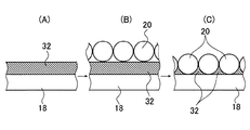
ところで、図6(A)〜(C)に示すように、ビーズ20の固定に先立ち、前述の如くビーズ20と接触する層32の上にあるビーズ20を押圧し、または沈降させて支持シート18に接触させてもよい。
すなわち、図6(A)に示すように、支持シート18上にビーズ20との接触層32を、例えば、図2(A)に示す発色材層24や図3(A)に示す発色材層24を塗布等により、形成した後、図6(B)に示すように、接触層32上に全面的にビーズ20を散布する。次に、接触層32上のビーズ20を押圧したり、沈降させたりすることにより、図6(C)に示すように、ビーズ20を支持シート18に接触させることができる。
【0055】
なお、図示しないが、ビーズ20を、発色材層24(図2(B)参照)や発色材層24(図4(A)参照)などに固定するのに先立って、バインダ25(図2(B),図2(C)参照)やバインダ30(図4(A)参照)上のビーズ20を押圧したり、沈降させたりすることにより、下層の発色材層24に接触させることもできるのは、もちろんである。
本発明の第1の態様の光拡散板、光拡散板の製造方法および本発明の第2の態様の表示装置は、基本的に以上のように構成される。
【0056】
次に、図7〜図9を参照して、本発明の第2の態様の表示装置の別の実施態様である画像表示装置について、詳細に説明する。
図7に、本発明の適用された画像表示装置の一例を概念的に示す。
図7に示される画像表示装置40は、図1に示される表示装置10と一部を除いて同一の構成要素を有するので、同一の構成要素には同一の参照符号を付し、その詳細な説明は省略し、異なる部分を主に説明する。
【0057】
図7に示される画像表示装置40は、画像の表示手段として液晶パネル12を利用する、いわゆる液晶ディスプレイ(LCD)である。画像表示装置40は、液晶パネル12と、液晶パネル12に光を入射するバックライト部14aと、液晶パネル12の表面に貼られ、液晶パネル12を通過した画像を担持する光を拡散する光拡散板16fと、さらにその上に貼られた外光散乱防止シート42とを有する。また、液晶パネル12には、マトリクス構造を有するカラーフィルタ(図示省略)が付設されるとともに、液晶パネル12を駆動するドライバ(図示省略)が接続され、さらに、画像表示装置40には、公知のLCDが有する各種の部材が必要に応じて配置される。
【0058】
また、本実施形態では、画像表示装置40の表示デバイスとしてLCDを用いているが、LCDに限定されるものではなく、マトリクス構造を有するものであれば、CRTでもPDPでもよい。
バックライト部14aも、画像の観察に充分な光量の光を射出可能なものであれば、コリメート光を射出する前述のバックライト部14も含め、各種の光源装置が全て利用可能である。なお、バックライト部14aから射出される光も特にコリメート光である必要はない。むしろ、ピクセリゼーションの抑制(デピクセリゼーション)のためには、光を拡散させ画像をぼけさせた方がよいので、コリメート光でない方が好ましい。
【0059】
光拡散板16fは、光学的な屈折力(光学的なパワー)を有し、かつ、画像表示装置40の観察者が視認することができない、微細な、球形等の構造を有している。
図8に、光拡散板16fの一例の概念図を示す。
図8に示される光拡散板16fは、光透過性の支持シート18に、光透過性の球体(以下、ビーズ20とする)をバインダ44によって固定してなる構成を有する。また、ビーズ20は、一部が支持シート18に接触している。
もちろん、本発明においては光拡散板16fとしては、上述した光拡散板16(16a〜16e)を用いるものである。
【0060】
本実施形態では、前述したようにバックライト光はとくにコリメートされておらず、好ましくは、バインダ44に光透過性のあるものを用いることで、図8に矢印で示されるように、液晶パネル12を通過した、画像を担持する光が、様々な方向から球形のビーズ20に入射し、該ビーズ20によって屈折されるため、充分に拡散される。
【0061】
バインダ44には特に限定はなく、ビーズ20を支持シート18に固定できれば、各種の接着剤が利用可能である。なお、本実施形態では、バインダ44は、光透過性を有するものであるのが好ましい。例えば、上述したバインダ25や30に用いられるバインダ材料を用いることができる。
【0062】
図9に、光拡散板16fと外光散乱防止シート42を拡大して示す。
外光散乱防止シート42は、光を吸収し、光透過率を落として外光の散乱を防止するものであり、特に限定されるものではないが、表面42aにAR処理を施すのが好ましい。外光散乱防止シート42としては、例えば、パーソナルコンピュータ等のモニタに取り付けて用いられるVDT(Visual Display Terminal)フィルタ(視覚表示端末用フィルタ)が好適に例示される。
【0063】
例えば、外光散乱防止シート42の光透過率が30%であるとすると、図9に矢印Aで示されるような、外光散乱防止シート42を一回透過する光は、入射光(100%)のうち、30%だけが透過する。一方、図9に矢印Bで示されるように、外から外光散乱防止シート42に入射し、光拡散板16fのビーズ20で反射され再び外光散乱シート42通過して行く光は、外光散乱シート42を2回通過するため、その透過率は30%の30%で、0.3×0.3=0.09、より9%となる。従って、外光の反射光の透過率は、外光散乱シート42の透過率の二乗で落ちるため、このように極めて小さくなり、外光の散乱が効果的に防止される。
【0064】
このように、本実施形態では、光拡散板16fをLCD12の表面に貼り付け、LCD12を通過した光を拡散させて、LCD12のマトリクス構造を視認できないようにさせ、なめらかで自然な画像を得ることができる。
また、このとき、光拡散板16fの上に外光散乱防止シート42を貼り付けることで、外光が光拡散板16fのビーズ20で散乱しコントラストを低下させるのを防止している。その結果、コントラストを落とさずに、デピクセリゼーションすることができ、例えば、特に医療に適用した場合には、診断に適したなめらかで自然な画像を画像表示装置に表示することができる。
【0065】
なお、上述したように、外光散乱防止シートは、その透過率を故意に落とし、外光の影響をその透過率の二乗にまで落とす、いわばCRTのフェースプレートの機能を有するものである。外光散乱防止シートを光拡散板の上に貼らずに、光拡散板の支持シートに外光散乱防止シートの機能を持たせるようにしてもよい。この場合、支持シートを、光透過率が例えば30%程度となるようにすればよい。
【0066】
以上、本発明に係る光拡散板、光拡散板の製造方法および表示装置について、種々の実施例を挙げて詳細に説明したが、本発明はこれらの実施例に限定されず、本発明の要旨を逸脱しない範囲において、各種の改良や設計の変更を行ってもよいのは、もちろんである。例えば、光拡散板も、本実施形態ではビーズを用いたものであったが、これに限定されるものではない。
【0067】
【発明の効果】
以上、詳細に説明したように、本発明の第1の態様の光拡散板の製造方法によって製造される光拡散板および本発明の第1の態様の光拡散板は、優れた光拡散性能を有する上に、外光の反射および散乱も少なく、かつ耐光性も高い、優れた特性を有する光拡散板である。
また、本発明の第2の態様の表示装置は、このような優れた特性を持つ本発明の第1の態様の光拡散板を用いているので、光拡散板のもつ優れた光拡散性能、および外光反射の低減によって、広い視野角に渡って良好なコントラスト比を有し、医療用の用途にも好適に利用可能な液晶ディスプレイである。
【0068】
本発明の第2の態様によれば、さらに、コントラストを落とさずに、表示画像のギザギザを解消すること(デピクセリゼーション)ができ、なめらかで自然な画像を画像表示装置に表示することができる。
従って、特に本発明を医療に適用した場合には、診断に適したなめらかで自然な画像が得られ、特にその効果を発揮することができる。
【図面の簡単な説明】
【図1】 本発明の表示装置の一実施例を概念的に示す分解斜視図である。
【図2】 (A)および(B)は、それぞれ本発明の光拡散板の一実施例を概念的に示す断面模式図である。
【図3】 (A)は、本発明の光拡散板の一実施例の製造工程の一例を概念的に示す断面模式図であり、(B)は、(A)で製造された光拡散板の断面模式図であり、(C)は、その使用形態の一例を概念的に示す断面模式図である。
【図4】 (A)は、本発明の光拡散板の別の実施例の製造工程の一例を概念的に示す断面模式図であり、(B)は、(A)で製造された光拡散板の断面模式図であり、(C)は、その使用形態の一例を概念的に示す断面模式図である。
【図5】 (A)は、本発明の光拡散板の別の実施例の製造工程の一例を概念的に示す断面模式図であり、(B)は、(A)で製造された光拡散板の断面模式図であり、(C)は、その使用形態の一例を概念的に示す断面模式図である。
【図6】 (A),(B)および(C)は、それぞれ本発明の光拡散板の別の実施例を製造する工程を概念的に示す断面模式図である。
【図7】 本発明の画像表示装置の一実施例を示す概念図である。
【図8】 図7に示す画像表示装置の液晶パネルと光拡散板を示す概略図である。
【図9】 図7に示す画像表示装置の光拡散板と外光散乱防止シートを示す概略図である。
【符号の説明】
10,40 (画像)表示装置
12 液晶パネル
14,14a バックライト部
16,16a16b,16c,16d,16e,16f 光拡散板
18 支持シート
20 ビーズ
25,30,44 バインダ
23 光非反射処理層
22 第1発色材層(ポジ型感光性発色材料)
24 発色材層(感光性発色材料)
31 第2発色材層(ネガ型感光性発色材料)
32 接触層
42 外光散乱防止シート[0001]
BACKGROUND OF THE INVENTION
The present invention provides a light diffusion plate, Manufacturing method of light diffusion plateAnd a light diffusing plate capable of realizing a liquid crystal display having a wide viewing angle and displaying a high-contrast image.Manufacturing method of light diffusing plate for manufacturing such a light diffusing plateAnd thisTheyThe present invention relates to a display device such as a liquid crystal display device using an optical diffusion plate or an image display device having a matrix structure.
[0002]
[Prior art]
In recent years, with the spread of word processors, personal computers, and the like, various image display devices have been developed and used for displaying images.
An image display apparatus is generally composed of a display device that converts an image information electrical signal into image light and displays it on a display screen, a drive circuit that drives the display device, and a power source that supplies power to the drive circuit. The There are various image display devices depending on the optical method of display and the driving method of the display device. Conventionally, the most popular is a CRT (Cathode Ray Tube) display. For example, in the medical field such as ultrasonic diagnosis, CT diagnosis, and MRI diagnosis, a black and white CRT display is used. Since this black and white CRT display does not have a digital matrix structure, a smooth and natural image can be obtained. it can.
[0003]
On the other hand, recently, liquid crystal displays (hereinafter referred to as LCDs) have come to be used in various fields because of their advantages such as easy miniaturization, thinness, and light weight. In particular, the frequency of use of LCDs as word processors and computer displays has increased significantly. In addition, the use of the LCD is also considered as a monitor for medical diagnostic apparatuses, which have conventionally been mainstream, such as ultrasonic diagnostic apparatuses, CT diagnostic apparatuses, and MRI diagnostic apparatuses.
[0004]
[Problems to be solved by the invention]
As described above, the LCD has many advantages such as being easy to miniaturize, thin and lightweight, but has poor viewing angle characteristics (narrow viewing angle), that is, an image depending on the viewing direction and angle. The contrast ratio of the image is drastically reduced, and gradation inversion occurs, resulting in a different image appearance. Therefore, there is a problem that the image cannot be properly observed depending on the position of the observer.
In particular, in medical applications such as those described above, diagnosis is performed based on the density of the image, so an image with a high contrast ratio is required, and improper recognition of the image may be a cause of misdiagnosis or a difference in diagnosis results. Become. Therefore, an image having a high contrast ratio over a wide viewing angle is particularly required. Further, in a medical monitor, since the display image is usually a monochrome image, the image contrast depending on the viewing angle is drastically lowered, which is more problematic.
[0005]
In addition, as LCDs with a wide viewing angle, LCDs such as IPS (In-Plane Swiching) mode and MVA (Multi-domain Vertical Alignement) mode are also known, but these are also suitable for monochrome images, especially for medical use. On the other hand, a sufficiently wide viewing angle has not been secured.
On the other hand, as an LCD that can obtain an image with a good contrast ratio over a wide viewing angle, collimated light (straight-ahead light) is used as the backlight (collimated backlight), and light that has passed through the liquid crystal panel is diffused. A method of diffusing with a plate is known.
However, an LCD that uses a diffusion plate to achieve a sufficient viewing angle even in medical applications has not yet been realized. In addition, in the method using a diffusion plate, external light incident on the diffusion plate is also reflected and scattered, which reduces the contrast of the observation image, and it is often impossible to observe a suitable image. .
[0006]
On the other hand, a high-definition display with a clear digital pixel matrix structure, high sharpness, and LCD like the LCD is suitable for displaying an artificial image such as CG (Computer Graphics).
However, since the LCD has a matrix structure of digital pixels, for example, for a still image having a natural smoothness such as an X-ray image, the clarity of this matrix structure gives a mosaic feeling. Therefore, there is a problem that an undesired state of so-called pixelization (or jaggy) occurs in which the image is jagged. This is particularly noticeable when the pixel size is large (for example, 15 ″ XGA (Extended Graphics Array) and the pixel size is about 300 μm), the vertical streaks of the matrix structure of the color filter can be clearly seen.
Further, not only the LCD but also a color CRT, a PDP (Plasma Display Panel) or the like having a matrix structure similarly has the problem that the above pixelation occurs.
[0007]
The first problem of the present invention is to solve the above-mentioned problems of the prior art, have excellent light diffusion performance, and suitably reduce contrast reduction due to surface reflection, and is used for a liquid crystal display. Light diffusion plate with higher light resistance that has a good contrast ratio over a wide viewing angle and can realize a liquid crystal display suitable for medical useAnd light diffusing plate manufacturing methodIs to provide.
The second problem of the present invention is to solve the above-mentioned problems of the prior art and to eliminate a pixelization (jaggy) (that is, to depixelize) a liquid crystal display device using the light diffusion plate. An object of the present invention is to provide a display device capable of obtaining a smooth and natural display image.
[0008]
[Means for Solving the Problems]
In order to achieve the first object, the light diffusion plate of the first aspect of the present inventionManufacturing methodHas a light-transmitting support, a light-transmitting sphere that forms a diffusion layer, and a photosensitive coloring material interposed between the support and the sphere.When manufacturing the light diffusion plate
This photosensitive coloring material contains at least a diazonium salt, a coupler, and a base, and after development, the non-exposed area is colored and the exposed area is non-colored.IsThen, substantially parallel light is incident on the sphere and the photosensitive coloring material from the diffusion layer side, and the photosensitive coloring material is exposed to light condensed by the sphere, and then the photosensitive coloring material is heated and developed. The non-exposed portion of the photosensitive coloring material is colored, and the exposed portion is non-colored.MakeIt is characterized by that.
Here, it is preferable that at least one of the diazonium salt, the coupler, and the base is included in a microcapsule.
[0009]
The photosensitive color forming material preferably forms a photosensitive color forming material layer between the support and the diffusion layer.
The photosensitive coloring material is preferably a material that contacts the sphere.
The light diffusion plate of the present inventionManufacturing methodEach of the above light diffusion platesManufacturing methodBecauseThe light diffusion plate isFurthermore, it has the material which contacts the said sphere, The said photosensitive coloring material is distribute | arranged between the material which contacts the said sphere, and the said support body, It is characterized by the above-mentioned.
Moreover, it is preferable that the material which contacts the said spherical body contains the light absorption material.
The diffusion layer is preferably formed by embedding the sphere after first forming a layer of a material in contact with the sphere.
Moreover, it is preferable that the surface on the opposite side to the said diffused layer of the said support body is given the light non-reflective process.
Moreover, it is preferable that the reflectance with respect to external light is 10% or less by the effect | action of the said color development area | region (light non-passing area | region).
[0010]
Also,In order to achieve the first problem,Of the present inventionOf the first aspectThe light diffusing plate is disposed between a light-transmitting support, a light-transmitting sphere that forms a diffusion layer, a material that contacts the sphere, a material that contacts the sphere, and the support. A first photosensitive coloring material, and the first photosensitive coloring material contains at least a diazonium salt, a coupler, and a base, and after development, the non-exposed portion develops color, the exposed portion becomes non-colored, and the sphere The material in contact is a second photosensitive coloring material that develops color at the exposed portion after development, and substantially parallel light is incident on the sphere and the first and second photosensitive coloring materials from the diffusion layer side. The second photosensitive color forming material is exposed by the substantially parallel light, and the first photosensitive color forming material is exposed by the light incident on the sphere and collected by the sphere, and then the first and the first 2Develop the photosensitive coloring material The exposed portion of the second photosensitive coloring material and the non-exposed portion of the first photosensitive coloring material are colored, and the exposed portion of the first photosensitive coloring material is non-colored. The development of the photosensitive coloring material is a heat development.
Here, it is preferable that at least one of the diazonium salt, the coupler, and the base is contained in a microcapsule.
[0011]
The second photosensitive color forming material is a negative silver halide photosensitive emulsion, and the development thereof is preferably photographic emulsion development, fixing and washing treatment.
Alternatively, the second photosensitive color developing material is preferably a negative photosensitive heat developing material containing a triphenylmethane leuco dye precursor, a photo acid generator, a photo radical generator and a radical quencher.
The first photosensitive coloring material preferably contains a light absorbing material.
The diffusion layer is preferably formed by embedding the sphere after first forming a layer of a material in contact with the sphere.
Moreover, it is preferable that the surface on the opposite side to the said diffused layer of the said support body is given the light non-reflective process.
[0012]
The light diffusing plate of the present invention includes a light-transmitting support, a light-transmitting sphere that forms a diffusion layer, a material that contacts the sphere, a material that contacts the sphere, and the support. A first photosensitive color-forming material disposed on the first photosensitive color-forming material, wherein the first photosensitive color-forming material develops a color at a non-exposed portion after development and an exposed portion becomes non-color-developed, and the material that contacts the sphere is developed A second photosensitive coloring material that develops an exposed portion later, substantially parallel light is incident on the sphere and the first and second photosensitive coloring materials from the diffusion layer side; After exposing the second photosensitive coloring material and exposing the first photosensitive coloring material with light incident on the sphere and collected by the sphere, the first and second photosensitive coloring materials are exposed. And developing to expose the exposed portion and the front of the second photosensitive coloring material. The non-exposed portion of the first photosensitive coloring material is colored, and the exposed portion of the first photosensitive coloring material is non-colored. The surface of the support opposite to the diffusion layer is It is characterized by being subjected to light non-reflection treatment.
[0013]
In order to solve the second problem, a display device according to a second aspect of the present invention includes a liquid crystal display panel, a backlight unit that emits parallel light to the liquid crystal display panel, and the liquid crystal display panel. In contrast, it is arranged on the opposite side of the backlight part.A light diffusing plate manufactured by the method of manufacturing a light diffusing plate of the first aspect;the aboveOf the first aspectAnd a light diffusing plateThe
Here, it is preferable that the light diffusing plate has an invisible structure having optical refractive power and is disposed on the observation side of the display screen of an image display device having a matrix structure.
The diffusion layer is preferably formed by fixing the light-transmitting sphere to a binder.
Moreover, it is preferable that an external light scattering prevention sheet is further provided on the light diffusion plate provided on the observation side of the display screen.
[0014]
DETAILED DESCRIPTION OF THE INVENTION
Light diffusing plate according to the present invention, Manufacturing method of light diffusion plateThe display device and the display device will be described in detail below on the basis of preferred embodiments shown in the accompanying drawings.
[0015]
FIG. 1 conceptually shows an embodiment of a display device according to the second aspect of the present invention, which utilizes the light diffusing plate according to the first aspect of the present invention.
A
Since the
[0016]
The
Accordingly, the
[0017]
As long as the
[0018]
The
Moreover, it is preferable that the reflectance with respect to external light is 10% or less by the effect | action of this non-passing area | region.
[0019]
FIG. 2A shows a schematic cross-sectional schematic view of one embodiment of the light diffusion plate of the first aspect of the present invention.
The
[0020]
Therefore, as shown by a one-dot chain line in FIG. 2A, collimated light that is emitted from the
Therefore, according to the present invention, a display device 10 (LCD) that can obtain a good contrast ratio over a wide viewing angle can be realized.
[0021]
The
Specifically, various resin materials such as various glasses, polyesters, polyolefins, polyamides, polyethers, polystyrenes, polyester amides, polycarbonates, polyphenylene sulfides, polyether esters, polyvinyl chlorides, polymethacrylic acid esters and the like are preferable examples. Is done.
In addition, the
[0022]
Further, in order to make the observability of the
[0023]
The
In the
[0024]
The material of the
Further, the size of the
[0025]
The
[0026]
In addition, in the specification of Japanese Patent Application No. 2000-009136, the applicant of the present invention is a thermoresponsive microcapsule encapsulating an electron-donating colorless dye as a preferred example of such a positive color former, and an electron in the same molecule. Illustrative examples include a compound having a receiving portion and a polymerizable vinyl monomer portion, and a coloring material containing a photopolymerization initiator. In the color former, these compounds and photopolymerization initiator are present outside the heat-responsive microcapsules.
In this color former, the exposed portion is cured (polymerized) by the composition outside the heat-responsive microcapsule (set as a curable composition) and fixed, and the compound does not move by subsequent heating. In the unexposed area, the compound (electron-accepting compound or the electron-accepting compound having the above-mentioned electron-accepting part and polymerizable vinyl monomer part having mobility (not fixed) is moved in the coloring material by heating, It is a recording material for forming a positive image by coloring an electron-donating colorless dye in a capsule.
This coloring material is described in detail in JP-A-10-226174.
[0027]
In addition to this, as long as it is a positive type photosensitive material, a color developing material (photosensitive heat-developable recording material) disclosed in JP-A Nos. 3-87827 and 4-21252 can be suitably used. .
In the specification of Japanese Patent Application No. 2000-009136, the present applicant discloses the above-described positive photosensitive material as a positive color forming material applicable to a light diffusion plate. Higher light resistance than light diffusing plates using positive photosensitive materialsLight diffusion plate 16Is to provide.
[0028]
Thus, the light diffusion plate of the present invention having high light resistance16Examples of the
That is, the present inventionInA preferred example of the
As a preferred form of this photosensitive coloring material, an oil-soluble diazonium salt is included in a microcapsule, and a coupler and a base are emulsified and dispersed together with other sensitizers and the like and arranged on the outside of the capsule. is there. In the exposed part, the diazonium salt loses the coupling function and does not develop color, whereas in the unexposed part, the coupler, base and sensitizer melted by heating enter the capsule and undergo a coupling reaction with the diazonium salt. Causes color development.
This coloring material is described in detail in JP-A-4-261893.
[0029]
As another preferred example, the photosensitive color developing material in which the exposed portion becomes non-colored is a positive silver halide photosensitive emulsion, and the developing means for color developing the unexposed portion is a photographic development, fixing and washing treatment. And a photosensitive material characterized by the following.
Preferable examples of this positive type silver halide photosensitive emulsion include a direct reversal emulsion for microdupe film and a direct reversal emulsion for X-ray duplication.
In ordinary negative silver halide emulsions, photosensitive nuclei are generated in the exposed areas, which are reduced to metallic silver by development to form a black image. In this positive photosensitive emulsion, If fogging is performed in advance and a desensitizing dye is added thereto, the exposed portion is not reduced, and the non-exposed portion is reduced to form colored silver.
These positive type direct reversal emulsions are described in, for example, “Science Photo Handbook” published by Maruzen Shoten.
For the development, fixing and washing with water of these positive silver halide light-sensitive emulsions, ordinary black-and-white emulsion processing solutions are preferably used.
[0030]
There is no particular limitation on the method of manufacturing such a
[0031]
FIG. 2B shows a schematic cross-sectional schematic diagram of another embodiment of the light diffusion plate of the present invention.
The
The
[0032]
A
Accordingly, also with this
[0033]
Such a
First, the
Next, the
[0034]
When the
Note that the light passing (transmitting) region composed of the contact region between the
[0035]
Next, the color developing material layer (the color developing material) 24 is developed with heat or a developing solution for photographic emulsion, so that only the unexposed portion is colored to become a light non-passing region. Become. As described above, the color developed by this development is only in the region where the light refracted by the
[0036]
In this embodiment, when the
[0037]
Further, although not particularly limited, when the
Further, in this embodiment, the amount ratio between the
[0038]
By the way, as shown in FIGS. 3 (A) and 4 (A), in the case where the color developing
[0039]
For this reason, FIG.BDiffusion plate shown in16cAnd Figure 4 (BDiffusion plate shown in16dIs produced, the color developing material layer (photosensitive material layer) 24 itself or its upper layer (a layer close to the exposure light source), for example, the
In addition, although the material used for the
[0040]
As a result, the gap between the beads 20 (for example, the
[0041]
Therefore, the diffusion plate as shown in FIG.16cIs produced as a binder for bonding the
For example, first, a
[0042]
Thereafter, as shown in FIG. 3A, when collimated light is incident as exposure light from the
[0043]
Thereafter, by developing the color developing
As shown in FIG. 3C, the diffusion plate thus obtained16c, The light carrying the image transmitted through the
[0044]
Also, a diffusion plate as shown in FIG.16dIs first formed on the
Thereafter, as shown in FIG. 4 (A), when collimated light is incident as exposure light from the
[0045]
Thereafter, by developing the color developing
As shown in FIG. 4C, the diffusion plate thus obtained16d, The light carrying the image transmitted through the
[0046]
In the above embodiment, when the color
[0047]
Next, still another embodiment of the present invention will be described with reference to FIG.
Each light scattering plate shown in FIGS. 5 (A) to (C)16eFIG. 4 shows each light scattering plate shown in FIG.16dThe difference is that a negative photosensitive material (layer) 31 is used instead of the
That is, this light diffusion plate16eFirst, a layer of a positive photosensitive material 22 (hereinafter referred to as a first color developing material layer 22) is disposed on a
[0048]
After arranging each material in this way, as shown in FIG. 5 (A), when these materials are exposed to light collimated from the side of the
Note that the blackened portion of the negative photosensitive layer of the second
[0049]
As an example of the negative
[0050]
Further, as another example of the negative
This type of photosensitive material includes a leuco dye precursor such as leuco crystal violet, a photoacid generator such as bromomethylphenylsulfone, and a photoradical generator such as lophine dimer in a microcapsule. In addition to the above, a radical quencher such as phenidone can be used. In this photosensitive material, radicals are generated in the photosensitive material and leuco crystal violet is oxidized to develop color, whereas in the unexposed part, the radical quencher enters the capsule by the subsequent heat treatment, causing color development. Due to this mechanism, the negative photosensitive material is stable. These are described in JP-A-5-61190 and JP-A-9-218482.
[0051]
Such a negative
[0052]
In these embodiments, the positive coloring material and the negative coloring material having the same developing means or developing method are used for the first
[0053]
That is, the positive color forming material used for the first color forming
Also,Second coloring material layer 31The negative color-developing material used in the present invention may be any negative photosensitive color-developing material, such as the negative-type black-and-white silver halide emulsions and negatives of the conventional negative-type black-and-white silver halide photosensitive materials described above. Type photosensitive heat-sensitive material.
[0054]
By the way, as shown in FIGS. 6A to 6C, prior to fixing the
That is, as shown in FIG. 6A, the
[0055]
Although not shown, prior to fixing the
The light diffusion plate of the first aspect of the present invention, Manufacturing method of light diffusion plateThe display device according to the second aspect of the present invention is basically configured as described above.
[0056]
Next, an image display device which is another embodiment of the display device according to the second aspect of the present invention will be described in detail with reference to FIGS.
FIG. 7 conceptually shows an example of an image display device to which the present invention is applied.
Since the
[0057]
The
[0058]
In this embodiment, an LCD is used as the display device of the
As long as the
[0059]
The
FIG. 8 shows a conceptual diagram of an example of the
The
Of course, in the present invention, the light diffusion plate 16 (16a to 16e) described above is used as the
[0060]
In the present embodiment, as described above, the backlight light is not particularly collimated, and preferably, by using a light-transmitting
[0061]
The
[0062]
In FIG.Light diffusion plate 16fThe outside light
The external light scattering
[0063]
For example, assuming that the light transmittance of the external light scattering
[0064]
As described above, in this embodiment, the
At this time, the external light scattering
[0065]
As described above, the external light scattering prevention sheet has a function of a CRT faceplate, that is, a function of deliberately reducing the transmittance and reducing the influence of external light to the square of the transmittance. You may make it give the function of an external light scattering prevention sheet to the support sheet of a light diffusion plate, without sticking an external light scattering prevention sheet on a light diffusion plate. In this case, the support sheet may have a light transmittance of about 30%, for example.
[0066]
As described above, the light diffusion plate according to the present invention., Manufacturing method of light diffusion plateAlthough the present invention has been described in detail with reference to various embodiments, the present invention is not limited to these embodiments, and various improvements and design changes are made without departing from the scope of the present invention. Of course, it's also good. For example, the light diffusing plate also uses beads in the present embodiment, but is not limited to this.
[0067]
【The invention's effect】
As explained in detail above,A light diffusion plate manufactured by the method for manufacturing a light diffusion plate according to the first aspect of the present invention, andThe light diffusing plate of the first aspect of the present invention is a light diffusing plate having excellent characteristics such as excellent light diffusing performance, little reflection and scattering of external light, and high light resistance.
Moreover, since the display device of the second aspect of the present invention uses the light diffusion plate of the first aspect of the present invention having such excellent characteristics, the excellent light diffusion performance of the light diffusion plate, The liquid crystal display has a good contrast ratio over a wide viewing angle by reducing external light reflection, and can be suitably used for medical applications.
[0068]
According to the second aspect of the present invention, the jaggedness of the display image can be eliminated without reducing the contrast (depixelation), and a smooth and natural image can be displayed on the image display device. it can.
Therefore, particularly when the present invention is applied to medical treatment, a smooth and natural image suitable for diagnosis can be obtained, and the effect can be exhibited particularly.
[Brief description of the drawings]
FIG. 1 is an exploded perspective view conceptually showing an embodiment of a display device of the present invention.
FIGS. 2A and 2B are schematic cross-sectional views conceptually showing an embodiment of a light diffusion plate of the present invention.
3A is a schematic cross-sectional view conceptually showing an example of a manufacturing process of an embodiment of the light diffusing plate of the present invention, and FIG. 3B is a light diffusing plate manufactured in FIG. (C) is a schematic cross-sectional view conceptually showing an example of the usage pattern.
4A is a schematic cross-sectional view conceptually showing an example of a manufacturing process of another embodiment of the light diffusing plate of the present invention, and FIG. 4B is a light diffusing manufactured in FIG. It is a section schematic diagram of a board, and (C) is a section schematic diagram showing an example of the form of use conceptually.
5A is a schematic cross-sectional view conceptually showing an example of a manufacturing process of another embodiment of the light diffusing plate of the present invention, and FIG. 5B is a light diffusing manufactured in FIG. It is a section schematic diagram of a board, and (C) is a section schematic diagram showing an example of the form of use conceptually.
FIGS. 6A, 6B, and 6C are schematic cross-sectional views conceptually showing processes for manufacturing another embodiment of the light diffusion plate of the present invention.
FIG. 7 is a conceptual diagram showing an embodiment of an image display device of the present invention.
8 is a schematic view showing a liquid crystal panel and a light diffusing plate of the image display device shown in FIG.
9 is a schematic view showing a light diffusion plate and an external light scattering prevention sheet of the image display device shown in FIG.
[Explanation of symbols]
10, 40 (image) display device
12 LCD panel
14, 14a Backlight part
16, 16a16b, 16c, 16d, 16e, 16f Light diffusing plate
18 Support sheet
20 beads
25, 30, 44 Binder
23 Light non-reflective treatment layer
22 First coloring material layer (positive photosensitive coloring material)
24 Coloring material layer (photosensitive coloring material)
31 Second coloring material layer (negative photosensitive coloring material)
32 Contact layer
42 Outside light scattering prevention sheet
Claims (20)
この感光性発色材料は、少なくともジアゾニウム塩、カプラーおよび塩基を含み、現像後に、非露光部が発色し、露光部が非発色となるものであり、
前記拡散層側から前記球体および前記感光性発色材料に略平行光を入射し、前記球体によって集光された光によって前記感光性発色材料を露光した後に、
前記感光性発色材料を加熱現像して、前記感光性発色材料の非露光部を発色させ、露光部を非発色とさせることを特徴とする光拡散板の製造方法。A light transmissive support, upon producing an optically transparent spheres forming a diffusion layer, a light diffusion plate for chromatic and photosensitive color material which is interposed between the support and the spherical,
The photosensitive coloring material comprises at least diazonium salt, a coupler and a base, after development, color development is non-exposed portion, the exposed portions Ri shall Der such a non-color,
After substantially parallel light is incident on the sphere and the photosensitive coloring material from the diffusion layer side, and the photosensitive coloring material is exposed by the light collected by the sphere,
It said photosensitive coloring material to heat development to the photosensitive allowed to develop the unexposed portions of the color forming material, manufacturing method of the light diffusion plate, characterized in that makes the exposed portion and the non-color.
前記光拡散板は、さらに、前記球体に接触する材料を有し、
前記感光性発色材料は、前記球体に接触する材料と前記支持体との間に配されていることを特徴とする光拡散板の製造方法。It is a manufacturing method of the light diffusing plate in any one of Claims 1-3,
The light diffusing plate further includes a material that contacts the sphere,
The method of manufacturing a light diffusing plate , wherein the photosensitive coloring material is disposed between a material that contacts the sphere and the support.
前記第1感光性発色材料は、少なくともジアゾニウム塩、カプラーおよび塩基を含み、現像後に、非露光部が発色し、露光部が非発色となり、
前記球体に接触する材料は、現像後に、露光部が発色する第2感光性発色材料であり、
前記拡散層側から前記球体および前記第1および前記第2感光性発色材料に略平行光を入射し、
入射した略平行光によって前記第2感光性発色材料を露光するとともに、前記球体に入射して前記球体によって集光された光によって前記第1感光性発色材料を露光した後に、
前記第1および前記第2感光性発色材料を現像して、前記第2感光性発色材料の露光部および前記第1感光性発色材料の非露光部を発色させ、前記第1感光性発色材料の露光部を非発色とさせてなるものであり、
前記第1感光性発色材料の現像は、加熱現像であることを特徴とする光拡散板。A light-transmitting support, a light-transmitting sphere that forms a diffusion layer, a material that contacts the sphere, and a first photosensitive color that is disposed between the material that contacts the sphere and the support. With materials,
The first photosensitive coloring material contains at least a diazonium salt, a coupler, and a base, and after development, the non-exposed portion is colored, and the exposed portion is non-colored,
The material that comes into contact with the sphere is a second photosensitive coloring material that develops an exposed portion after development,
From the diffusion layer side, substantially parallel light is incident on the sphere and the first and second photosensitive coloring materials,
After exposing the second photosensitive coloring material with incident substantially parallel light and exposing the first photosensitive coloring material with light incident on the sphere and collected by the sphere,
The first and second photosensitive color developing materials are developed to develop an exposed portion of the second photosensitive color developing material and a non-exposed portion of the first photosensitive color developing material. The exposed area is non-colored,
The light diffusing plate according to claim 1, wherein the development of the first photosensitive coloring material is heat development.
クロカプセルに包含されていることを特徴とする請求項9に記載の光拡散板。The light diffusing plate according to claim 9 , wherein at least one of the diazonium salt, the coupler, and the base is included in a microphone capsule.
その現像は、写真乳剤用現像、定着、水洗処理である請求項9または10に記載の光拡散板。The second photosensitive coloring material is a negative type silver halide photosensitive emulsion,
The light diffusing plate according to claim 9 or 10 , wherein the development is photographic emulsion development, fixing, and washing treatment.
前記第1感光性発色材料は、現像後に、非露光部が発色し、露光部が非発色となり、
前記球体に接触する材料は、現像後に、露光部が発色する第2感光性発色材料であり、
前記拡散層側から前記球体および前記第1および前記第2感光性発色材料に略平行光を入射し、
入射した略平行光によって前記第2感光性発色材料を露光するとともに、前記球体に入射して前記球体によって集光された光によって前記第1感光性発色材料を露光した後に、
前記第1および前記第2感光性発色材料を現像して、前記第2感光性発色材料の露光部および前記第1感光性発色材料の非露光部を発色させ、前記第1感光性発色材料の露光部を非発色とさせてなるものであり、
前記支持体の前記拡散層と逆側の面が、光非反射処理を施されていることを特徴とする光拡散板。A light-transmitting support, a light-transmitting sphere that forms a diffusion layer, a material that contacts the sphere, and a first photosensitive color that is disposed between the material that contacts the sphere and the support. With materials,
The first photosensitive color developing material, after development, the non-exposed portion is colored, the exposed portion is non-colored,
The material that comes into contact with the sphere is a second photosensitive coloring material that develops an exposed portion after development,
From the diffusion layer side, substantially parallel light is incident on the sphere and the first and second photosensitive coloring materials,
After exposing the second photosensitive coloring material with incident substantially parallel light and exposing the first photosensitive coloring material with light incident on the sphere and collected by the sphere,
The first and second photosensitive color developing materials are developed to develop an exposed portion of the second photosensitive color developing material and a non-exposed portion of the first photosensitive color developing material. The exposed area is non-colored,
A light diffusing plate, wherein a surface of the support opposite to the diffusion layer is subjected to a light non-reflection treatment.
Priority Applications (4)
| Application Number | Priority Date | Filing Date | Title |
|---|---|---|---|
| JP2000053391A JP4132546B2 (en) | 2000-02-29 | 2000-02-29 | Light diffusing plate, method for manufacturing light diffusing plate, and display device |
| EP01104786A EP1130421A3 (en) | 2000-02-29 | 2001-02-27 | Light diffusing plate and display apparatus |
| US09/794,399 US20010035926A1 (en) | 2000-02-29 | 2001-02-28 | Light diffusing plate and display apparatus |
| US12/164,398 US20090009701A1 (en) | 2000-02-29 | 2008-06-30 | Light Diffusing Plate and Display Apparatus |
Applications Claiming Priority (1)
| Application Number | Priority Date | Filing Date | Title |
|---|---|---|---|
| JP2000053391A JP4132546B2 (en) | 2000-02-29 | 2000-02-29 | Light diffusing plate, method for manufacturing light diffusing plate, and display device |
Publications (3)
| Publication Number | Publication Date |
|---|---|
| JP2001242309A JP2001242309A (en) | 2001-09-07 |
| JP2001242309A5 JP2001242309A5 (en) | 2005-11-10 |
| JP4132546B2 true JP4132546B2 (en) | 2008-08-13 |
Family
ID=18574784
Family Applications (1)
| Application Number | Title | Priority Date | Filing Date |
|---|---|---|---|
| JP2000053391A Expired - Fee Related JP4132546B2 (en) | 2000-02-29 | 2000-02-29 | Light diffusing plate, method for manufacturing light diffusing plate, and display device |
Country Status (3)
| Country | Link |
|---|---|
| US (2) | US20010035926A1 (en) |
| EP (1) | EP1130421A3 (en) |
| JP (1) | JP4132546B2 (en) |
Families Citing this family (24)
| Publication number | Priority date | Publication date | Assignee | Title |
|---|---|---|---|---|
| WO2004097915A1 (en) | 2003-04-25 | 2004-11-11 | Semiconductor Energy Laboratory Co., Ltd. | Droplet discharging device, method for forming pattern and method for manufacturing semiconductor device |
| US7273773B2 (en) * | 2004-01-26 | 2007-09-25 | Semiconductor Energy Laboratory Co., Ltd. | Display device, method for manufacturing thereof, and television device |
| US7462514B2 (en) | 2004-03-03 | 2008-12-09 | Semiconductor Energy Laboratory Co., Ltd. | Semiconductor device and method for manufacturing the same, liquid crystal television, and EL television |
| US20050196710A1 (en) * | 2004-03-04 | 2005-09-08 | Semiconductor Energy Laboratory Co., Ltd. | Method for forming pattern, thin film transistor, display device and method for manufacturing the same, and television apparatus |
| KR101192973B1 (en) * | 2004-03-19 | 2012-10-24 | 가부시키가이샤 한도오따이 에네루기 켄큐쇼 | Method for forming pattern, thin film transistor, display device and method for manufacturing the same, and television device |
| US7642038B2 (en) * | 2004-03-24 | 2010-01-05 | Semiconductor Energy Laboratory Co., Ltd. | Method for forming pattern, thin film transistor, display device, method for manufacturing thereof, and television apparatus |
| US8158517B2 (en) | 2004-06-28 | 2012-04-17 | Semiconductor Energy Laboratory Co., Ltd. | Method for manufacturing wiring substrate, thin film transistor, display device and television device |
| US7820465B2 (en) * | 2006-03-02 | 2010-10-26 | Semiconductor Energy Laboratory Co., Ltd. | Manufacturing method for a circuit pattern, a thin film transistor and an electronic appliance |
| TW200838471A (en) * | 2007-03-26 | 2008-10-01 | Wells Technology Co Ltd Dr | X-ray film reading device |
| US20110043543A1 (en) * | 2009-08-18 | 2011-02-24 | Hui Chen | Color tuning for electrophoretic display |
| CN102483474B (en) * | 2009-11-25 | 2014-04-23 | 夏普株式会社 | Light diffusion polarizing sheet, method for producing light diffusion polarizing sheet, and display device |
| KR102081158B1 (en) | 2012-10-22 | 2020-02-25 | 엘지디스플레이 주식회사 | Wire mesh type diffuser plate and method of fabricating the same, and liquid crystal display device having the wire mesh type diffuser plate |
| CN105324709B (en) | 2013-05-17 | 2018-11-09 | 伊英克加利福尼亚有限责任公司 | Colour display device with colored filter |
| TWI534520B (en) | 2013-10-11 | 2016-05-21 | 電子墨水加利福尼亞有限責任公司 | Color display device |
| US9513527B2 (en) | 2014-01-14 | 2016-12-06 | E Ink California, Llc | Color display device |
| WO2015127045A1 (en) | 2014-02-19 | 2015-08-27 | E Ink California, Llc | Color display device |
| US10380955B2 (en) | 2014-07-09 | 2019-08-13 | E Ink California, Llc | Color display device and driving methods therefor |
| US10891906B2 (en) | 2014-07-09 | 2021-01-12 | E Ink California, Llc | Color display device and driving methods therefor |
| US10147366B2 (en) | 2014-11-17 | 2018-12-04 | E Ink California, Llc | Methods for driving four particle electrophoretic display |
| CN109564927B (en) | 2016-07-29 | 2023-06-20 | 特里纳米克斯股份有限公司 | Optical sensor and detector for optical detection |
| EP3532864A1 (en) | 2016-10-25 | 2019-09-04 | trinamiX GmbH | Detector for an optical detection of at least one object |
| EP3571522B1 (en) | 2016-11-17 | 2023-05-10 | trinamiX GmbH | Detector for optically detecting at least one object |
| TWI714347B (en) | 2017-11-14 | 2020-12-21 | 美商伊英克加利福尼亞有限責任公司 | Electrophoretic active delivery system including porous conductive electrode layer |
| CN114728155B (en) | 2019-11-27 | 2024-04-26 | 伊英克公司 | Benefit agent delivery system including microcells with electrolytic seal layers |
Family Cites Families (20)
| Publication number | Priority date | Publication date | Assignee | Title |
|---|---|---|---|---|
| DE2448063C2 (en) * | 1974-10-09 | 1984-06-07 | Agfa-Gevaert Ag, 5090 Leverkusen | Color photographic recording material |
| US4127693A (en) * | 1975-02-10 | 1978-11-28 | Lemelson Jerome H | Reflex reflectors with pyramid-shaped indentations |
| US4299906A (en) * | 1979-06-01 | 1981-11-10 | American Hoechst Corporation | Light-sensitive color proofing film with surfactant in a light-sensitive coating |
| JP2701994B2 (en) * | 1990-01-30 | 1998-01-21 | 富士写真フイルム株式会社 | Photosensitive and thermosensitive recording materials |
| US5563738A (en) * | 1993-09-03 | 1996-10-08 | Jenmar Visual Systems | Light transmitting and dispersing filter having low reflectance |
| JP3127067B2 (en) * | 1993-11-08 | 2001-01-22 | 富士写真フイルム株式会社 | Diazo thermal recording material |
| WO1995031754A1 (en) * | 1994-05-11 | 1995-11-23 | Minnesota Mining And Manufacturing Company | Improved imaging process for imaging materials |
| TW373116B (en) * | 1994-12-15 | 1999-11-01 | Sharp Kk | Lighting apparatus |
| US5626800A (en) * | 1995-02-03 | 1997-05-06 | Minnesota Mining And Manufacturing Company | Prevention of groove tip deformation in brightness enhancement film |
| US5629785A (en) * | 1995-05-04 | 1997-05-13 | Motorola, Inc. | Polymer dispersed liquid crystal display device with asymmetric optical diffuser |
| US5751387A (en) * | 1995-07-28 | 1998-05-12 | Fujitsu Limited | Fresnel lens and liquid crystal display device |
| EP0853774B1 (en) * | 1995-10-06 | 2001-11-07 | Polaroid Corporation | Holographic medium and process |
| US6007960A (en) * | 1996-04-23 | 1999-12-28 | Agfa-Gevaert | Process for producing a colored image with reduced dot gain and colored image obtained thereby |
| US6262840B1 (en) * | 1996-05-30 | 2001-07-17 | Sony Corporation | Plano lens, rear-projection type projector screen employing the same, and rear-projection type video display apparatus |
| JPH10226174A (en) * | 1996-11-19 | 1998-08-25 | Fuji Photo Film Co Ltd | Photosensitive thermal recording material |
| JP4171933B2 (en) * | 1997-09-12 | 2008-10-29 | ソニー株式会社 | Planar lens manufacturing method |
| JPH11156951A (en) * | 1997-12-01 | 1999-06-15 | Sony Corp | Method for turning spherical body arrangement into image, measuring method and device, and manufacture of piano lens and device therefor |
| US6137258A (en) * | 1998-10-26 | 2000-10-24 | General Electric Company | System for speed-sensorless control of an induction machine |
| US6778239B2 (en) * | 1999-01-18 | 2004-08-17 | Fuji Photo Film Co., Ltd. | Light diffusing plate and display apparatus |
| JP2000275411A (en) * | 1999-01-18 | 2000-10-06 | Fuji Photo Film Co Ltd | Collimating plate and backlight system |
-
2000
- 2000-02-29 JP JP2000053391A patent/JP4132546B2/en not_active Expired - Fee Related
-
2001
- 2001-02-27 EP EP01104786A patent/EP1130421A3/en not_active Withdrawn
- 2001-02-28 US US09/794,399 patent/US20010035926A1/en not_active Abandoned
-
2008
- 2008-06-30 US US12/164,398 patent/US20090009701A1/en not_active Abandoned
Also Published As
| Publication number | Publication date |
|---|---|
| EP1130421A3 (en) | 2002-09-11 |
| US20010035926A1 (en) | 2001-11-01 |
| US20090009701A1 (en) | 2009-01-08 |
| JP2001242309A (en) | 2001-09-07 |
| EP1130421A2 (en) | 2001-09-05 |
Similar Documents
| Publication | Publication Date | Title |
|---|---|---|
| JP4132546B2 (en) | Light diffusing plate, method for manufacturing light diffusing plate, and display device | |
| US6327091B1 (en) | Collimating plate and backlight system | |
| JP2001116917A (en) | Member to improve image quality and image display device using the same | |
| JP2854986B2 (en) | Reflective image forming and display device viewed with holographic diffused ambient light | |
| US6657766B2 (en) | Reflective display device and retro-reflector used therefor | |
| US6424395B1 (en) | Light scattering film and liquid crystal display device | |
| JP2001242309A5 (en) | ||
| TW200402574A (en) | Mask, substrate with light reflective film, method for manufacturing light reflective film, liquid crystal display device, and electronic apparatus | |
| JP2000171619A (en) | Anisotropic light scattering film and liquid crystal display device using the same | |
| US6778239B2 (en) | Light diffusing plate and display apparatus | |
| JP2003295167A (en) | Liquid crystal display device | |
| JP2000298205A (en) | Optical diffusing plate and display device | |
| JPH11212491A (en) | Single sheet type display with patternable conductive trace | |
| JP4590729B2 (en) | Off-axis anisotropic light scattering film and display device using the same | |
| JP2002341333A (en) | Translucent liquid crystal display device and manufacturing method therefor | |
| JP3407641B2 (en) | Liquid crystal devices and electronic equipment | |
| JP2004240136A (en) | Method for manufacturing pattern layer formed body with various levels | |
| JP2005055620A (en) | Reflective display element | |
| JP3731414B2 (en) | Off-axis anisotropic light scattering film and display device using the same | |
| JP2000275411A (en) | Collimating plate and backlight system | |
| JPH11212111A (en) | Display device having optical patterning enabled conductive trace | |
| JP3379427B2 (en) | Liquid crystal devices and electronic equipment | |
| JP3261853B2 (en) | Reflective liquid crystal display | |
| JPH06110076A (en) | Liquid crystal display device | |
| JP2002341331A (en) | Translucent color liquid crystal display device and back electrode substrate |
Legal Events
| Date | Code | Title | Description |
|---|---|---|---|
| A521 | Request for written amendment filed |
Free format text: JAPANESE INTERMEDIATE CODE: A523 Effective date: 20050906 |
|
| A621 | Written request for application examination |
Free format text: JAPANESE INTERMEDIATE CODE: A621 Effective date: 20050906 |
|
| A711 | Notification of change in applicant |
Free format text: JAPANESE INTERMEDIATE CODE: A712 Effective date: 20061214 |
|
| A977 | Report on retrieval |
Free format text: JAPANESE INTERMEDIATE CODE: A971007 Effective date: 20070806 |
|
| A131 | Notification of reasons for refusal |
Free format text: JAPANESE INTERMEDIATE CODE: A131 Effective date: 20070814 |
|
| A521 | Request for written amendment filed |
Free format text: JAPANESE INTERMEDIATE CODE: A523 Effective date: 20071015 |
|
| A131 | Notification of reasons for refusal |
Free format text: JAPANESE INTERMEDIATE CODE: A131 Effective date: 20071113 |
|
| A521 | Request for written amendment filed |
Free format text: JAPANESE INTERMEDIATE CODE: A523 Effective date: 20080115 |
|
| TRDD | Decision of grant or rejection written | ||
| A01 | Written decision to grant a patent or to grant a registration (utility model) |
Free format text: JAPANESE INTERMEDIATE CODE: A01 Effective date: 20080520 |
|
| A01 | Written decision to grant a patent or to grant a registration (utility model) |
Free format text: JAPANESE INTERMEDIATE CODE: A01 |
|
| A61 | First payment of annual fees (during grant procedure) |
Free format text: JAPANESE INTERMEDIATE CODE: A61 Effective date: 20080602 |
|
| FPAY | Renewal fee payment (event date is renewal date of database) |
Free format text: PAYMENT UNTIL: 20110606 Year of fee payment: 3 |
|
| R150 | Certificate of patent or registration of utility model |
Free format text: JAPANESE INTERMEDIATE CODE: R150 |
|
| LAPS | Cancellation because of no payment of annual fees |