JP4128319B2 - Multi-chip bonding method and apparatus - Google Patents
Multi-chip bonding method and apparatus Download PDFInfo
- Publication number
- JP4128319B2 JP4128319B2 JP36616399A JP36616399A JP4128319B2 JP 4128319 B2 JP4128319 B2 JP 4128319B2 JP 36616399 A JP36616399 A JP 36616399A JP 36616399 A JP36616399 A JP 36616399A JP 4128319 B2 JP4128319 B2 JP 4128319B2
- Authority
- JP
- Japan
- Prior art keywords
- substrate
- bonding
- wafer ring
- supply
- adhesive
- Prior art date
- Legal status (The legal status is an assumption and is not a legal conclusion. Google has not performed a legal analysis and makes no representation as to the accuracy of the status listed.)
- Expired - Fee Related
Links
Images


Classifications
-
- H—ELECTRICITY
- H01—ELECTRIC ELEMENTS
- H01L—SEMICONDUCTOR DEVICES NOT COVERED BY CLASS H10
- H01L21/00—Processes or apparatus adapted for the manufacture or treatment of semiconductor or solid state devices or of parts thereof
- H01L21/67—Apparatus specially adapted for handling semiconductor or electric solid state devices during manufacture or treatment thereof; Apparatus specially adapted for handling wafers during manufacture or treatment of semiconductor or electric solid state devices or components ; Apparatus not specifically provided for elsewhere
- H01L21/67005—Apparatus not specifically provided for elsewhere
- H01L21/67011—Apparatus for manufacture or treatment
- H01L21/67144—Apparatus for mounting on conductive members, e.g. leadframes or conductors on insulating substrates
-
- H—ELECTRICITY
- H01—ELECTRIC ELEMENTS
- H01L—SEMICONDUCTOR DEVICES NOT COVERED BY CLASS H10
- H01L21/00—Processes or apparatus adapted for the manufacture or treatment of semiconductor or solid state devices or of parts thereof
- H01L21/02—Manufacture or treatment of semiconductor devices or of parts thereof
- H01L21/04—Manufacture or treatment of semiconductor devices or of parts thereof the devices having at least one potential-jump barrier or surface barrier, e.g. PN junction, depletion layer or carrier concentration layer
- H01L21/50—Assembly of semiconductor devices using processes or apparatus not provided for in a single one of the subgroups H01L21/06 - H01L21/326, e.g. sealing of a cap to a base of a container
- H01L21/60—Attaching or detaching leads or other conductive members, to be used for carrying current to or from the device in operation
-
- Y—GENERAL TAGGING OF NEW TECHNOLOGICAL DEVELOPMENTS; GENERAL TAGGING OF CROSS-SECTIONAL TECHNOLOGIES SPANNING OVER SEVERAL SECTIONS OF THE IPC; TECHNICAL SUBJECTS COVERED BY FORMER USPC CROSS-REFERENCE ART COLLECTIONS [XRACs] AND DIGESTS
- Y10—TECHNICAL SUBJECTS COVERED BY FORMER USPC
- Y10S—TECHNICAL SUBJECTS COVERED BY FORMER USPC CROSS-REFERENCE ART COLLECTIONS [XRACs] AND DIGESTS
- Y10S438/00—Semiconductor device manufacturing: process
- Y10S438/907—Continuous processing
Landscapes
- Engineering & Computer Science (AREA)
- Physics & Mathematics (AREA)
- Condensed Matter Physics & Semiconductors (AREA)
- General Physics & Mathematics (AREA)
- Manufacturing & Machinery (AREA)
- Computer Hardware Design (AREA)
- Microelectronics & Electronic Packaging (AREA)
- Power Engineering (AREA)
- Die Bonding (AREA)
- Container, Conveyance, Adherence, Positioning, Of Wafer (AREA)
Description
【0001】
【発明の属する技術分野】
本発明は、ハイブリット半導体装置の製造工程におけるマルチチップボンディング方法及び装置に関する。
【0002】
【従来の技術】
ハイブリット半導体装置は、図2に示すように、基板1に品種の異なる例えば2品種の半導体チップ2A、2Bを実装している。このように、基板1に品種の異なる半導体チップ2A、2Bを実装するマルチチップボンディング方法及び装置として、次のような方法が知られている。
【0003】
第1の方法は図3に示すように、1つの基板1毎にウェーハリング4(4A、4B・・)又はトレーを交換する方法である。以下、ウェーハリングの場合について説明する。
【0004】
図3に示すように、図示しないウェーハシート上に貼り付けられたウェーハ3は、縦横に格子状に分割して引き伸ばされて個々の半導体チップ2(2A、2B・・・)となっている。ウェーハシートの外周部はウェーハリング4(4A、4B・・・)に取付けられている。ウェーハリング4(4A、4B・・・)は、上下に一定間隔を保って積層する形でウェーハリングカセット5に収納されており、ウェーハリングカセット5は図示しないエレベータ装置に位置決め保持されている。ここで、ウェーハリングカセット5には、異なった品種の半導体チップ2A、2B・・・を有するウェーハリング4A、4B・・・が収納されている。即ち、半導体チップ2Aを有するウェーハリング4A、半導体チップ2Bを有するウェーハリング4B・・・等が収納されている。
【0005】
ウェーハリングカセット5の収納口側には一定距離離れてウェーハリング等保持装置6が配設されている。ウェーハリング等保持装置6のピックアップ位置7の下方には、半導体チップ2(2A、2B・・・)を突き上げる突き上げ針(図示せず)が配設されている。ウェーハリングカセット5内のウェーハリング4(4A、4B・・・)は、図示しないウェーハリング搬送手段によりチャックされてウェーハリング等保持装置6に搬送されて位置決め保持される。またウェーハリング等保持装置6に保持されたウェーハリング4(4A、4B・・・)は、ウェーハリング搬送手段によりチャックされてウェーハリングカセット5の元の位置に収納される。
【0006】
前記したウェーハリングカセット5、該ウェーハリングカセット5を位置決め保持する図示しないエレベータ装置、ウェーハリング等保持装置6及び図示しないウェーハリング搬送手段は、例えば特開平9−64147号公報、特開平9−64148号公報等が挙げられる。
【0007】
一方、基板1は、ローダ部10の基板カセット11に収納されており、基板カセット11より送り出された基板1は、基板搬送装置12により搬送され、基板1のボンディング部に接着材滴下装置20により接着材が滴下され、続いてボンディング部にボンディング装置30により半導体チップ2(2A、2B・・・)がボンディングされアンローダ部13の基板カセット14に収納される。
【0008】
接着材滴下装置20は、接着材を収納したプリフォームノズル21を有し、プリフォームノズル21は、Xテーブル22とYテーブル23とからなる周知のXYテーブル24のYテーブル23に上下動可能に設けられている。ボンディング装置30は、半導体チップ2(2A、2B・・・)を真空吸着保持して基板1にボンディングするボンディングツール31を有し、ボンディングツール31は、Xテーブル32とYテーブル33とからなる周知のXYテーブル34のYテーブル33に上下動可能に設けられている。
【0009】
次に作用について説明する。説明を簡単にするため、図2に示すように、基板1に2品種の半導体チップ2A、2Bをボンディングする場合について説明する。ウェーハリングカセット5内のウェーハリング4Aは、図示しないウェーハリング搬送手段により搬送され、ウェーハリング等保持装置6に位置決め保持される。そして、ピックアップされる半導体チップ2Aがピックアップ位置7に移動させられる。
【0010】
一方、ローダ部10の基板カセット11内の基板1が基板搬送装置12上に送り出される。基板1が基板搬送装置12によって接着材滴下装置20の接着材滴下ステーション部に搬送されて位置決めされると、接着材滴下装置20のXYテーブル24のXY軸方向の移動及びプリフォームノズル21の上下動により、基板1のボンディング部(図2の場合は6箇所)に接着材が滴下される。続いて接着材が滴下された基板1が基板搬送装置12によってボンディング装置30のボンディングステーションに搬送されて位置決めされると、後記する方法によってボンディング装置30のボンディングツール31がウェーハリング4A上の半導体チップ2Aを吸着保持して基板1の上方に移送し、基板1の半導体チップ2Aがボンディングされるボンディング部に半導体チップ2Aをボンディングする。
【0011】
前記したボンディングツール31によるウェーハリング4A上の半導体チップ2Aの吸着保持、基板1上への移送及びボンディングは次のように行われる。XYテーブル34によりボンディングツール31がピックアップ位置7の上方に移動して下降し、ピックアップ位置7の下方に配設された図示しない突き上げ針が上昇する。これにより、半導体チップ2Aを突き上げ、ボンディングツール31は半導体チップ2Aを真空により吸着保持する。ボンディングツール31は上昇し、XYテーブル34により基板1の半導体チップ2Aがボンディングされるボンディング部の上方に移動する。続いてボンディングツール31は下降し、基板1の前記ボンディング部に半導体チップ2Aをボンディングする。ボンディング後、ボンディングツール31の真空が切れ、ボンディングツール31は上昇する。前記したようにウェーハリング4Aより半導体チップ2Aがピックアップされると、次にピックアップされる半導体チップ2Aがピックアップ位置7に移動させられる。
【0012】
図2に示す基板1には、4個の半導体チップ2Aがボンディングされるので、前記したボンディングツール31がウェーハリング4Aより半導体チップ2Aを吸着保持して移送し、基板1のボンディング部に半導体チップ2Aをボンディングする動作は4回行われる。
【0013】
基板1への半導体チップ2Aのボンディングが全て終了すると、ウェーハリング等保持装置6に保持されたウェーハリング4Aは、図示しないウェーハリング搬送装置で搬送されてウェーハリングカセット5の元の位置に収納される。次にウェーハリングカセット5が図示しないエレベータ装置により上下動させられ、ウェーハリング4Bが搬送レベルに移動し、ウェーハリングカセット5内のウェーハリング4Bはウェーハリング搬送装置により搬送されてウェーハリング等保持装置6に位置決め保持される。
【0014】
そして、前記した方法により、ボンディングツール31がウェーハリング4Bより半導体チップ2Bを吸着保持して移送し、基板1の半導体チップ2Bがボンディングされるボンディング部に半導体チップ2Bがボンディングされる。図2に示す基板1には、2個の半導体チップ2Bがボンディングされるので、前記した半導体チップ2Bのボンディングは2回行われる。
【0015】
このようにして1枚の基板1への半導体チップ2A、2Bのボンディングが全て終了すると、基板1は基板搬送装置12により搬送されてアンローダ部13の基板カセット14内に収納される。前記した一連の工程によりローダ部10の基板カセット11内の基板1は、順次基板搬送装置12により搬送され、接着材滴下装置20によるボンディング部への接着材の滴下、ボンディング装置30によるボンディング部への半導体チップ2A、2Bのボンディングが行われる。この場合、半導体チップ2Aをボンディングするには、前記したようにウェーハリング等保持装置6にウェーハリング4Aが保持され、半導体チップ2Bをボンディングする場合にはウェーハリング4Aがウェーハリング4Bと交換されてウェーハリング等保持装置6にウェーハリング4Bが保持される。
【0016】
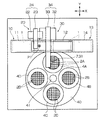
第2の方法は図4に示すように、品種の異なる複数のウェーハリング4A乃至4D又はトレーがウェーハリング等保持装置40に保持され、所望とするウェーハリング4A乃至4D又はトレーを選択的にピックアップ位置7に移動させる方法である。この場合もウェーハリング4A乃至4Dの場合について説明する。
【0017】
図4に示すように、ウェーハリング等保持装置40は、XY軸方向に駆動されると共に、中心軸41を中心として回転自在に支承され、図示しない回転駆動手段で回転させられる。またウェーハリング等保持装置40には、図4の例では品種の異なる4個のウェーハリング4A乃至4Dが位置決め保持されている。その他の構成であるローダ部10、基板カセット11、基板搬送装置12、アンローダ部13、基板カセット14、接着材滴下装置20及びボンディング装置30は図3と同じである。またウェーハリング等保持装置40のピックアップ位置7の下方には、半導体チップ2A乃至2Dを突き上げ針(図示せず)が配設されている。
【0018】
次に作用について説明する。この方法についても説明を簡単にするため、図2に示すように基板1に2種の半導体チップ2A、2Bをボンディングする場合について説明する。図4に示す方法は、図3に示す方法と次の点が異なるのみである。
【0019】
図3の方法は、1つの基板1における半導体チップ2Aのボンディング部にウェーハリング等保持装置6に保持されたウェーハリング4Aの半導体チップ2Aを全てボンディングした後、ウェーハリング等保持装置6に保持されているウェーハリング4Aをウェーハリング4Bに交換した後、前記基板1における半導体チップ2Bのボンディング部に半導体チップ2Bを全てボンディングした。その後、この全ての半導体チップ2A、2Bがボンディングされた基板1をアンローダ部13の基板カセット14に収納した。
【0020】
図4の方法は、ウェーハリング等保持装置40を回転させてウェーハリング4Aのピックアップされる半導体チップ2Aをピックアップ位置7に移動させる。そして、図3の場合と同様に、1つの基板1における半導体チップ2Aのボンディング部にウェーハリング4Aの半導体チップ2Aを全てボンディングした後、ウェーハリング等保持装置40を回転させてウェーハリング4Bのピックアップされる半導体チップ2Bをピックアップ位置7に移動させ、図3の場合と同様に、前記基板1にある半導体チップ2Bのボンディング部にウェーハリング4Bの半導体チップ2Bを全てボンディングする。その後、この全ての半導体チップ2A、2Bがボンディングされた基板1をアンローダ部13の基板カセット14に収納する。
【0021】
【発明が解決しようとする課題】
図3に示す第1の方法は、1つの基板1に対する半導体チップ2Aをボンディングするボンディング部にウェーハリング等保持装置6に保持されたウェーハリング4Aの半導体チップ2Aを全てボンディングした後、ウェーハリング等保持装置6に保持されたウェーハリング4Aをウェーハリング4Bと交換し、前記基板1に対する半導体チップ2Bをボンディングするボンディング部にウェーハリング等保持装置6に保持されたウェーハリング4Bの半導体チップ2Bを全てボンディングする。即ち、1つの基板1毎にウェーハリング4(4A、4B・・・)を交換する必要があるので、ウェーハリング4(4A、4B・・・)の交換頻度が多く、生産性が悪いという問題があった。
【0022】
図4に示す第2の方法は、ウェーハリング等保持装置40に複数のウェーハリング4A乃至4Dを保持させ、所望とするウェーハリング4A乃至4Dの選択は、ウェーハリング等保持装置40を回転させるのみで行えるので、生産性に優れている。しかし、ウェーハリング等保持装置40が大型化し、また装置が複雑になるという問題があった。図4の例では4個のウェーハリング4A乃至4Dを保持する場合を図示したが、5個以上のウェーハリングを保持させる場合には、更に大型化する。
【0023】
本発明の課題は、ウェーハリング等保持装置が大型化することもなく、かつ生産性の向上が図れるマルチチップボンディング方法及び装置を提供することにある。
【0024】
【課題を解決するための手段】
上記課題を解決するための本発明の手段は、基板を搬送する基板搬送装置と、この基板搬送装置の両端にそれぞれ設けられた第1及び第2の基板供給収納部と、前記基板搬送装置により搬送された基板のボンディング部に接着材を滴下する接着材滴下装置と、前記基板の接着材が滴下されたボンディング部に電子部品をボンディングするボンディング装置と、電子部品を有するウェーハリング又はトレーを保持するウェーハリング等保持装置とを備え、前記ウェーハリング等保持装置には、前記基板にボンディングする第1品種の電子部品を有する第1のウェーハリング又はトレーを保持し、前記第1の基板供給収納部から複数個の基板を基板搬送装置に順次送り出し、該基板の前記第1品種の電子部品をボンディングするボンディング部の全てに順次前記ウェーハリング等保持装置上の第1品種の電子部品をボンディングし、このボンディング完了後の基板を順次前記第2の基板供給収納部に収納し、その後、前記ウェーハリング等保持装置に保持された第1のウェーハリング又はトレーを前記基板にボンディングする第2品種の電子部品を有する第2のウェーハリング又はトレーにウェーハリング搬送装置によって交換して前記ウェーハリング等保持装置で保持し、前記第2の基板供給収納部に収納された基板を順次基板搬送装置に送り出し、これらの基板に前記第2品種の電子部品をボンディングするボンディング部の全てに順次前記ウェーハリング等保持装置上の第2品種の電子部品をボンディングし、このボンディング完了後の基板を順次前記第1の基板供給収納部に収納することを少なくとも行うマルチチップボンディング装置において、
前記接着材滴下装置のプリフォームノズルは、前記ボンディング装置のボンディングツールを保持するYテーブルと前記第1の基板供給収納部間と、前記Yテーブルと前記第2の基板供給収納部間に移動可能に構成され、前記第1の基板供給収納部から基板が送り出され時は、前記プリフォームノズルは、前記Yテーブルと前記第1の基板供給収納部間に位置して前記第1品種の電子部品のボンディング部に接着材が滴下され、前記第2の基板供給収納部から基板が送り出され時は、前記プリフォームノズルは、前記Yテーブルと前記第2の基板供給収納部間に位置して前記第2品種の電子部品のボンディング部に接着材が滴下されることを特徴とする。
【0027】
【発明の実施の形態】
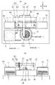
本発明の一実施の形態を図1により説明する。本実施の形態は、図3に示す方法の改良に関する。そこで、図3と同じ部材には同一符号を付して説明する。本実施の形態は、図3に示す構成及び方法が次の点で異なる。
【0028】
まず、構成の異なる点について説明する。図3に示すローダ部10及びアンローダ部13は、本実施の形態においてはそれぞれ第1、第2の基板供給収納部50、51となっている。また図3の基板搬送装置12は、ローダ部10からアンローダ部13にのみ基板1を搬送するようになっていたが、本実施の形態の基板搬送装置45は、第1の基板供給収納部50の基板カセット11より送り出された基板1を第2の基板供給収納部51の基板カセット14へ搬送して収納できると共に、第2の基板供給収納部51の基板カセット14より送り出された基板1を第1の基板供給収納部50の基板カセット11へ搬送して収納できるようになっている。
【0029】
また図3の接着材滴下装置20のプリフォームノズル21は、ボンディング装置30のYテーブル33とローダ部10間のみ移動可能に配設されている。本実施の形態の接着材滴下装置60のプリフォームノズル61は、ボンディング装置30のYテーブル33と第1の基板供給収納部50間は勿論のこと、Yテーブル33と第2の基板供給収納部51間も移動可能に構成されている。即ち、接着材滴下装置60のXテーブル61は、第1の基板供給収納部50側から第2の基板供給収納部51側に伸びてボンディング装置30のYテーブル33の上方に配設されている。そこで、プリフォームノズル21が上下動可能に設けられたYテーブル62とXテーブル61とでXYテーブル63を構成している。
【0030】
本実施の形態のその他のウェーハリングカセット5、ウェーハリング等保持装置6及びボンディング装置30は、それぞれ図3の構成とほぼ同じ構成となっているので、その説明は省略する。
【0031】
次に作用について説明する。説明を簡単にするため、図2に示すように、基板1に2品種の半導体チップ2A、2Bをボンディングする場合について説明する。ウェーハリングカセット5内のウェーハリング4Aは、図示しないウェーハリング搬送手段により搬送され、ウェーハリング等保持装置6に位置決め保持される。そして、ピックアップされる半導体チップ2Aがピックアップ位置7に移動させられる。
【0032】
一方、第1の基板供給収納部50の基板カセット11内の基板1が基板搬送装置45上に送り出される。基板1が基板搬送装置45によって接着材滴下装置60の接着材滴下ステーション部に搬送されて位置決めれると、接着材滴下装置60のXYテーブル63のXY軸方向の移動及びプリフォームノズル21の上下動により、基板1の半導体チップ2Aがボンディングされるボンディング部(図2の場合は4箇所)に接着材が滴下される。続いて接着材が滴下された基板1が基板搬送装置45によってボンディング装置30のボンディングステーションに搬送されて位置決めされると、後記する方法によってボンディング装置30のボンディングツール31がウェーハリング4A上の半導体チップ2Aを吸着保持して基板1の上方に移送し、基板1の半導体チップ2Aがボンディングされるボンディング部に半導体チップ2Aをボンディングする。
【0033】
前記したボンディングツール31によるウェーハリング4A上の半導体チップ2Aの吸着保持、基板1上への移送及びボンディングは、従来例と同様に次のように行われる。XYテーブル34によりボンディングツール31がピックアップ位置7の上方に移動して下降し、ピックアップ位置7の下方に配設された図示しない突き上げ針が上昇する。これにより、半導体チップ2Aを突き上げ、ボンディングツール31は半導体チップ2Aを真空により吸着保持する。ボンディングツール31は上昇し、XYテーブル34により基板1の半導体チップ2Aがボンディングされるボンディング部の上方に移動する。続いてボンディングツール31は下降し、基板1の前記ボンディング部に半導体チップ2Aをボンディングする。ボンディング後、ボンディングツール31の真空が切れ、ボンディングツール31は上昇する。前記したようにウェーハリング4Aより半導体チップ2Aがピックアップされると、次にピックアップされる半導体チップ2Aがピックアップ位置7に移動させられる。
【0034】
図2に示す基板1には、4個の半導体チップ2Aがボンディングされるので、前記したボンディングツール31がウェーハリング4Aより半導体チップ2Aを吸着保持して移送し、基板1のボンディング部に半導体チップ2Aをボンディングする動作は4回行われる。このようにして1枚の基板1への半導体チップ2Aのボンディングが全て終了すると、基板1は基板搬送装置45により搬送されて第2の基板供給収納部51の基板カセット14内に収納される。
【0035】
前記した一連の工程、即ち基板カセット11からの基板1の送り出し、基板1の半導体チップ2Aがボンディングされるボンディング部への接着材の滴下、基板1の半導体チップ2Aがボンディングされるボンディング部への半導体チップ2Aのボンディング、第2の基板供給収納部51の基板カセット14内に収納が、基板カセット11内の全ての基板1に対して行われる。
【0036】
基板カセット11内の全ての基板1に対して半導体チップ2Aのボンディングが終了して基板カセット14内に全て収納されると、基板1に対して半導体チップ2Bのボンディングが行われる。
【0037】
ウェーハリング等保持装置6に保持されたウェーハリング4Aは、図示しないウェーハリング搬送装置で搬送されてウェーハリングカセット5の元の位置に収納される。次にウェーハリングカセット5が図示しないエレベータ装置により上下動させられ、ウェーハリング4Bが搬送レベルに移動し、ウェーハリングカセット5内のウェーハリング4Bはウェーハリング搬送装置により搬送されてウェーハリング等保持装置6に位置決め保持される。
【0038】
またプリフォームノズル21が1点鎖線のように上昇し、Xテーブル61が駆動してYテーブルが2点鎖線のように、第2の基板供給収納部51とYテーブル33間の接着材滴下ステーション部に移動する。
【0039】
そして、今度は、第2の基板供給収納部51の基板カセット14内の基板1が基板搬送装置45上に送り出される。基板1が基板搬送装置45によって接着材滴下装置60の接着材滴下ステーション部に搬送されて位置決めされると、接着材滴下装置60のXYテーブル63のXY軸方向の移動及びプリフォームノズル21の上下動により、基板1の半導体チップ2Bがボンディングされるボンディング部(図2の場合は2箇所)に接着材が滴下される。続いて接着材が滴下された基板1が基板搬送装置45によってボンディング装置30のボンディングステーションに搬送されて位置決めされると、前記した方法によってボンディング装置30のボンディングツール31がウェーハリング4B上の半導体チップ2Bを吸着保持して基板1の上方に移送し、基板1の半導体チップ2Bがボンディングされるボンディング部に半導体チップ2Bをボンディングする。
【0040】
図2に示す基板1には、2個の半導体チップ2Bがボンディングされるので、前記したボンディングツール31がウェーハリング4Bより半導体チップ2Bを吸着保持して移送し、基板1のボンディング部に半導体チップ2Bをボンディングする動作は2回行われる。このようにして1枚の基板1への半導体チップ2Bのボンディングが全て終了すると、基板1は基板搬送装置45により搬送されて第1の基板供給収納部50の基板カセット11内に収納される。
【0041】
前記した一連の工程、即ち基板カセット14からの基板1の送り出し、基板1の半導体チップ2Bがボンディングされるボンディング部への接着材の滴下、基板1の半導体チップ2Bがボンディングされるボンディング部への半導体チップ2Bのボンディング、第1の基板供給収納部50の基板カセット11内に収納が、基板カセット14内の全ての基板1に対して行われる。
【0042】
このように、第1の基板供給収納部50の基板カセット11から複数個の基板1(実施の形態は基板カセット11内の基板1の全て)を基板搬送装置45に順次送り出し、該基板1の半導体チップ2Aをボンディングするボンディング部の全てに順次ウェーハリング等保持装置6上の半導体チップ2Aをボンディングする。このボンディング完了後の基板1を順次第2の基板供給収納部51の基板カセット14に収納する。その後、ウェーハリング等保持装置6に保持されたウェーハリング4Aを基板1にボンディングする半導体チップ2Bを有するウェーハリング4Bと交換してウェーハリング等保持装置6で保持する。そして、基板カセット14に収納された基板1を順次基板搬送装置45に送り出し、これらの基板1に半導体チップ2Bをボンディングするボンディング部の全てに順次ウェーハリング等保持装置6上の半導体チップ2Bをボンディングする。このボンディング完了後の基板1を順次基板カセット11に収納する。このため、ウェーハリング4(4A、4B・・・)の交換回数が大幅に減少し、生産性が向上する。またウェーハリング等保持装置6には1個のウェーハリング4(4A、4B・・・)を保持するのみでよいので、ウェーハリング等保持装置6が大型化することもない。
【0043】
本実施の形態においては、ウェーハリング等保持装置6にウェーハリング4(4A、4B・・・)を保持させた場合について説明したが、半導体チップ2A、2B・・・をそれぞれ収納したトレーを交換して保持させるようにしてもよい。
【0044】
また1つの基板1に2品種の半導体チップ2A、2Bをボンディングする場合について説明したが、3品種以上の半導体チップ2(2A、2B・・・)等をボンディングする場合も適用できることは言うまでもない。例えば3品種の半導体チップ2A、2B、2Cをボンディングする場合には、前記した方法により2品種の半導体チップ2A、2Bのボンディングが終了した基板1を収納した第1の基板供給収納部50の基板カセット11より更に基板1を基板搬送装置45に送り出し、実線で示す状態の接着材滴下装置60により半導体チップ2Cがボンディングされるボンディング部に接着材を滴下する。一方、ウェーハリング等保持装置6にはウェーハリング4Cを保持させる。そして、ボンディング装置30により基板1の半導体チップ2Cがボンディングされるボンディング部の全てに前記した方法により半導体チップ2Cをボンディングする。このボンディング終了後、基板搬送装置45により搬送して第2の基板供給収納部51に収納する。
【0045】
また本実施の形態においては、基板カセット11内の全ての基板1を順次送り出し、半導体チップ2Aのみをボンディングして基板カセット14内に収納し、その後基板カセット14内の全ての基板1を順次送り出し、半導体チップ2Bのみをボンディングして基板カセット11内に収納するように説明した。しかし、次の方法でもよい。第1、第2の基板供給収納部50、51にそれぞれ複数個の基板カセット11、14を設置し、第1の基板供給収納部50の1番目、2番目、3番目・・・の基板カセット11内の全ての基板1を順次送り出し、半導体チップ2Aのみをボンディングして第2の基板供給収納部51の1番目、2番目、3番目・・・の基板カセット14内に収納する。その後、第2の基板供給収納部51の1番目、2番目、3番目・・・の基板カセット14内の全ての基板1を順次送り出し、半導体チップ2Bのみをボンディングして第1の基板供給収納部50の1番目、2番目、3番目・・・の基板カセット11内に収納するようにしてもよい。
【0046】
また基板カセット11、14に変えて基板1を一時保持するバッファ部を設けてもよい。即ち、第1、第2の基板供給収納部50、51は、基板カセット11、14又はバッファ部に限定されなく、基板1のストック部であればよい。
【0048】
また電子部品として半導体チップの場合について説明したが、抵抗、コンデンサ等でもよいことは言うまでもい。
【0049】
【発明の効果】
本発明の請求項1又は2の構成によれば、ウェーハリング等保持装置が大型化することもなく、かつ生産性の向上が図れる。
【図面の簡単な説明】
【図1】本発明のマルチチップボンディング方法の一実施の形態を示し、(a)は平面図、(b)は一部断面正面図である。
【図2】ハイブリット半導体装置の1例を示す平面図である。
【図3】従来のマルチチップボンディング方法の1例を示す平面図である。
【図4】従来のマルチチップボンディング方法の他の例を示す平面図である。
【符号の説明】
1 基板
2(2A、2B・・・) 半導体チップ
3 ウェーハ
4(4A、4B・・・) ウェーハリング
5 ウェーハリングカセット
6 ウェーハリング等保持装置
7 ピックアップ位置
11、14 基板カセット
30 ボンディング装置
31 ボンディングツール
34 XYテーブル
45 基板搬送装置
50、51 基板供給収納部
60 接着材滴下装置
61 プリフォームノズル
63 XYテーブル[0001]
BACKGROUND OF THE INVENTION
The present invention relates to a multichip bonding method and apparatus in a manufacturing process of a hybrid semiconductor device.
[0002]
[Prior art]
In the hybrid semiconductor device, as shown in FIG. 2, different types of
[0003]
As shown in FIG. 3, the first method is a method of exchanging the wafer ring 4 (4A, 4B...) Or tray for each
[0004]
As shown in FIG. 3, the
[0005]
A
[0006]
The
[0007]
On the other hand, the
[0008]
The
[0009]
Next, the operation will be described. In order to simplify the description, a case where two types of
[0010]
On the other hand, the
[0011]
The above-described
[0012]
Since four
[0013]
When all the bonding of the
[0014]
Then, by the above-described method, the
[0015]
When the bonding of the
[0016]
In the second method, as shown in FIG. 4, a plurality of wafer rings 4A to 4D of different varieties or trays are holding devices such as wafer rings.40The wafer rings 4A to 4D or trays that are held in the desired position are selectively moved to the pickup position 7. Also in this case, the case of the wafer rings 4A to 4D will be described.
[0017]
As shown in FIG. 4, the wafer
[0018]
Next, the operation will be described. In order to simplify the description of this method, the case where two types of
[0019]
In the method of FIG. 3, after bonding all the semiconductor chips 2 </ b> A of the
[0020]
In the method of FIG. 4, the holding
[0021]
[Problems to be solved by the invention]
The first method shown in FIG. 3 is to bond all the
[0022]
In the second method shown in FIG. 4, a plurality of wafer rings 4 </ b> A to 4 </ b> D are held by the wafer
[0023]
An object of the present invention is to provide a multi-chip bonding method and apparatus capable of improving productivity without increasing the size of a holding device such as a wafer ring.
[0024]
[Means for Solving the Problems]
The present invention for solving the above problemshand ofThe stage includes a substrate transfer device for transferring a substrate, first and second substrate supply and storage units provided at both ends of the substrate transfer device, and a substrate transferred by the substrate transfer device.An adhesive dropping device for dropping an adhesive on the bonding portion of the substrate, and a bonding portion where the adhesive on the substrate is droppedA bonding device for bonding electronic components; and a wafer ring holding device for holding a wafer ring or tray having electronic components. The wafer ring holding device includes a first type of electronic component for bonding to the substrate. All of the bonding units that hold the first wafer ring or tray having the plurality of substrates from the first substrate supply and storage unit to the substrate transfer device and bond the electronic components of the first type on the substrate. The first kind of electronic components on the wafer ring holding device are sequentially bonded to each other, and the substrates after completion of the bonding are sequentially stored in the second substrate supply and storage unit, and then held on the wafer ring holding device. A second type of electronic component for bonding the first wafer ring or tray formed to the substrate; The substrate is exchanged to the second wafer ring or tray by the wafer ring transfer device and held by the holding device such as the wafer ring, and the substrates stored in the second substrate supply and storage unit are sequentially sent to the substrate transfer device. The second type electronic components on the wafer ring and other holding devices are sequentially bonded to all the bonding parts for bonding the second type electronic components to the first substrate supply and storage sequentially. At least to store in the departmentIn multi-chip bonding equipment,
The preform nozzle of the adhesive dripping device is movable between the Y table holding the bonding tool of the bonding device and the first substrate supply / storage unit, and between the Y table and the second substrate supply / storage unit. The preform nozzle is located between the Y table and the first substrate supply and storage unit when the substrate is sent out from the first substrate supply and storage unit. When the adhesive is dropped on the bonding portion of the substrate and the substrate is sent out from the second substrate supply and storage portion, the preform nozzle is positioned between the Y table and the second substrate supply and storage portion. Adhesive is dropped on the bonding part of the second kind of electronic componentsIt is characterized by that.
[0027]
DETAILED DESCRIPTION OF THE INVENTION
An embodiment of the present invention will be described with reference to FIG. The present embodiment relates to an improvement of the method shown in FIG. Therefore, the same members as those in FIG. This embodiment is different in the configuration and method shown in FIG.
[0028]
First, differences in configuration will be described. The
[0029]
Also, the
[0030]
The other
[0031]
Next, the operation will be described. In order to simplify the description, a case where two types of
[0032]
On the other hand, the
[0033]
The suction holding of the
[0034]
Since four
[0035]
The series of steps described above, that is, the delivery of the
[0036]
When the bonding of the
[0037]
The
[0038]
Further, the
[0039]
This time, the
[0040]
Since two
[0041]
The series of steps described above, that is, the delivery of the
[0042]
In this way, a plurality of substrates 1 (in the embodiment, all the
[0043]
In the present embodiment, the case where the wafer ring 4 (4A, 4B...) Is held by the wafer
[0044]
Further, the case where two kinds of
[0045]
Further, in the present embodiment, all the
[0046]
Further, instead of the
[0048]
Although the case of a semiconductor chip as an electronic component has been described, it goes without saying that it may be a resistor, a capacitor, or the like.
[0049]
【The invention's effect】
Of the present inventionAccording to the configuration of
[Brief description of the drawings]
1A and 1B show an embodiment of a multichip bonding method according to the present invention, in which FIG. 1A is a plan view and FIG.
FIG. 2 is a plan view showing an example of a hybrid semiconductor device.
FIG. 3 is a plan view showing an example of a conventional multi-chip bonding method.
FIG. 4 is a plan view showing another example of a conventional multi-chip bonding method.
[Explanation of symbols]
1 Substrate
2 (2A, 2B ...) Semiconductor chip
3 Wafer
4 (4A, 4B ...) Wafer ring
5 Wafer ring cassette
6 Wafer ring holding device
7 Pickup position
11, 14 Substrate cassette
30 Bonding equipment
31 Bonding tool
34 XY table
45 Substrate transfer device
50, 51 Substrate supply storage
60 Adhesive dropping device
61 preform nozzle
63 XY table
Claims (2)
前記接着材滴下装置のプリフォームノズルは、前記ボンディング装置のボンディングツールを保持するYテーブルと前記第1の基板供給収納部間と、前記Yテーブルと前記第2の基板供給収納部間に移動可能に構成され、前記第1の基板供給収納部から基板が送り出され時は、前記プリフォームノズルは、前記Yテーブルと前記第1の基板供給収納部間に位置して前記第1品種の電子部品のボンディング部に接着材が滴下され、前記第2の基板供給収納部から基板が送り出され時は、前記プリフォームノズルは、前記Yテーブルと前記第2の基板供給収納部間に位置して前記第2品種の電子部品のボンディング部に接着材が滴下されることを特徴とするマルチチップボンディング方法。 Adhesive material is dropped onto a substrate transfer device for transferring a substrate, first and second substrate supply and storage portions provided at both ends of the substrate transfer device, and a bonding portion of the substrate transferred by the substrate transfer device. The wafer ring comprising: an adhesive dropping device; a bonding device for bonding an electronic component to a bonding portion where the adhesive on the substrate is dropped; and a holding device such as a wafer ring or a tray for holding a tray. The equal holding device holds a first wafer ring or tray having a first kind of electronic component bonded to the substrate, and sequentially sends a plurality of substrates from the first substrate supply / accommodation unit to the substrate transfer device. The wafer ring and other holding devices are sequentially placed on all the bonding parts for bonding the first-type electronic components of the substrate. Bonding the first type of electronic components and sequentially storing the substrates after the bonding is completed in the second substrate supply / accommodating unit, and then the first wafer ring or tray held by the holding device such as the wafer ring is mounted. A second wafer ring or tray having a second type of electronic component bonded to the substrate is replaced by a wafer ring transfer device and held by the holding device such as the wafer ring, and is stored in the second substrate supply and storage unit. Next, the second type electronic components on the holding device such as the wafer ring are sequentially bonded to all the bonding parts for bonding the second type electronic components to these substrates. at least performing multichip ball to be housed sequentially said first substrate supply accommodating section the substrate after completion In the loading method,
The preform nozzle of the adhesive dripping device is movable between the Y table holding the bonding tool of the bonding device and the first substrate supply / storage unit, and between the Y table and the second substrate supply / storage unit. The preform nozzle is located between the Y table and the first substrate supply and storage unit when the substrate is sent out from the first substrate supply and storage unit. When the adhesive is dropped on the bonding portion of the substrate and the substrate is sent out from the second substrate supply and storage portion, the preform nozzle is positioned between the Y table and the second substrate supply and storage portion. A multi-chip bonding method, wherein an adhesive is dropped on a bonding portion of a second type of electronic component .
前記接着材滴下装置のプリフォームノズルは、前記ボンディング装置のボンディングツールを保持するYテーブルと前記第1の基板供給収納部間と、前記Yテーブルと前記第2の基板供給収納部間に移動可能に構成され、前記第1の基板供給収納部から基板が送り出され時は、前記プリフォームノズルは、前記Yテーブルと前記第1の基板供給収納部間に位置して前記第1品種の電子部品のボンディング部に接着材が滴下され、前記第2の基板 供給収納部から基板が送り出され時は、前記プリフォームノズルは、前記Yテーブルと前記第2の基板供給収納部間に位置して前記第2品種の電子部品のボンディング部に接着材が滴下されることを特徴とするマルチチップボンディング装置。 Adhesive material is dropped onto a substrate transfer device for transferring a substrate, first and second substrate supply and storage portions provided at both ends of the substrate transfer device, and a bonding portion of the substrate transferred by the substrate transfer device. The wafer ring comprising: an adhesive dropping device; a bonding device for bonding an electronic component to a bonding portion where the adhesive on the substrate is dropped; and a holding device such as a wafer ring or a tray for holding a tray. The equal holding device holds a first wafer ring or tray having a first kind of electronic component bonded to the substrate, and sequentially sends a plurality of substrates from the first substrate supply / accommodation unit to the substrate transfer device. The wafer ring and other holding devices are sequentially placed on all the bonding parts for bonding the first-type electronic components of the substrate. Bonding the first type of electronic components and sequentially storing the substrates after the bonding is completed in the second substrate supply / accommodating unit, and then the first wafer ring or tray held by the holding device such as the wafer ring is mounted. A second wafer ring or tray having a second type of electronic component bonded to the substrate is replaced by a wafer ring transfer device and held by the holding device such as the wafer ring, and is stored in the second substrate supply and storage unit. Next, the second type electronic components on the holding device such as the wafer ring are sequentially bonded to all the bonding parts for bonding the second type electronic components to these substrates. at least performing multichip ball to be housed sequentially said first substrate supply accommodating section the substrate after completion In the loading apparatus,
The preform nozzle of the adhesive dripping device is movable between the Y table holding the bonding tool of the bonding device and the first substrate supply / storage unit, and between the Y table and the second substrate supply / storage unit. The preform nozzle is located between the Y table and the first substrate supply and storage unit when the substrate is sent out from the first substrate supply and storage unit. When the adhesive is dropped on the bonding portion of the substrate and the substrate is sent out from the second substrate supply and storage portion, the preform nozzle is positioned between the Y table and the second substrate supply and storage portion. A multi-chip bonding apparatus , wherein an adhesive is dropped on a bonding portion of a second type of electronic component .
Priority Applications (4)
| Application Number | Priority Date | Filing Date | Title |
|---|---|---|---|
| JP36616399A JP4128319B2 (en) | 1999-12-24 | 1999-12-24 | Multi-chip bonding method and apparatus |
| TW089124040A TW533520B (en) | 1999-12-24 | 2000-11-14 | Multi-chip bonding method and apparatus |
| KR10-2000-0076964A KR100400106B1 (en) | 1999-12-24 | 2000-12-15 | Multichip bonding method and apparatus |
| US09/748,812 US6383844B2 (en) | 1999-12-24 | 2000-12-26 | Multi-chip bonding method and apparatus |
Applications Claiming Priority (1)
| Application Number | Priority Date | Filing Date | Title |
|---|---|---|---|
| JP36616399A JP4128319B2 (en) | 1999-12-24 | 1999-12-24 | Multi-chip bonding method and apparatus |
Publications (3)
| Publication Number | Publication Date |
|---|---|
| JP2001185565A JP2001185565A (en) | 2001-07-06 |
| JP2001185565A5 JP2001185565A5 (en) | 2006-04-27 |
| JP4128319B2 true JP4128319B2 (en) | 2008-07-30 |
Family
ID=18486081
Family Applications (1)
| Application Number | Title | Priority Date | Filing Date |
|---|---|---|---|
| JP36616399A Expired - Fee Related JP4128319B2 (en) | 1999-12-24 | 1999-12-24 | Multi-chip bonding method and apparatus |
Country Status (4)
| Country | Link |
|---|---|
| US (1) | US6383844B2 (en) |
| JP (1) | JP4128319B2 (en) |
| KR (1) | KR100400106B1 (en) |
| TW (1) | TW533520B (en) |
Families Citing this family (18)
| Publication number | Priority date | Publication date | Assignee | Title |
|---|---|---|---|---|
| JP3667241B2 (en) * | 2001-03-09 | 2005-07-06 | 松下電器産業株式会社 | Bonding method and apparatus |
| JP4800524B2 (en) * | 2001-09-10 | 2011-10-26 | ルネサスエレクトロニクス株式会社 | Semiconductor device manufacturing method and manufacturing apparatus |
| JP4390503B2 (en) | 2003-08-27 | 2009-12-24 | パナソニック株式会社 | Component mounting apparatus and component mounting method |
| US7244636B2 (en) * | 2005-10-19 | 2007-07-17 | Texas Instruments Incorporated | Semiconductor assembly for improved device warpage and solder ball coplanarity |
| EP1941536B8 (en) * | 2005-10-26 | 2019-06-19 | Kulicke and Soffa (Switzerland) Management GmbH | Method and device for the placement of electronic components, in particular semiconductor chips, on a substrate |
| JP4714026B2 (en) * | 2006-01-10 | 2011-06-29 | 株式会社東芝 | Electronic component mounting apparatus, electronic component mounting method, and electronic component apparatus |
| US7677431B2 (en) * | 2006-10-19 | 2010-03-16 | Asm Technology Singapore Pte Ltd. | Electronic device handler for a bonding apparatus |
| KR100787968B1 (en) | 2007-02-13 | 2007-12-24 | 세광테크 주식회사 | C.o.g apparatus having chip supplyer |
| EP2299486B1 (en) * | 2009-09-18 | 2015-02-18 | EV Group E. Thallner GmbH | Method for bonding chips to wafers |
| US8546802B2 (en) * | 2011-11-07 | 2013-10-01 | Taiwan Semiconductor Manufacturing Company, Ltd. | Pick-and-place tool for packaging process |
| US9105760B2 (en) | 2011-11-07 | 2015-08-11 | Taiwan Semiconductor Manufacturing Company, Ltd. | Pick-and-place tool for packaging process |
| JP5959949B2 (en) * | 2012-06-13 | 2016-08-02 | キヤノンマシナリー株式会社 | Chip mounting device |
| JP5959948B2 (en) * | 2012-06-13 | 2016-08-02 | キヤノンマシナリー株式会社 | Wafer ring exchange device and chip mounting device |
| KR101422401B1 (en) * | 2013-04-03 | 2014-07-22 | 세메스 주식회사 | Apparatus for bonding light-emitting device chips |
| TWI607587B (en) * | 2016-09-13 | 2017-12-01 | 台灣琭旦股份有限公司 | A Method For Fixing Chips |
| CN110891726B (en) * | 2017-04-04 | 2021-08-24 | 库利克和索夫工业公司 | Ultrasonic welding system and method of use |
| WO2023100831A1 (en) * | 2021-11-30 | 2023-06-08 | ボンドテック株式会社 | Chip periphery peeling apparatus, chip supply apparatus, chip supply system, chip bonding system, pickup apparatus, chip periphery peeling method, chip supply method, chip bonding method, and pickup method |
| CN115714101B (en) * | 2022-11-09 | 2023-11-14 | 长园半导体设备(珠海)有限公司 | Feeding device and switching method |
Family Cites Families (5)
| Publication number | Priority date | Publication date | Assignee | Title |
|---|---|---|---|---|
| US5528397A (en) * | 1991-12-03 | 1996-06-18 | Kopin Corporation | Single crystal silicon transistors for display panels |
| US5273622A (en) * | 1991-01-28 | 1993-12-28 | Sarcos Group | System for continuous fabrication of micro-structures and thin film semiconductor devices on elongate substrates |
| JP2666788B2 (en) * | 1995-10-19 | 1997-10-22 | 日本電気株式会社 | Manufacturing method of chip size semiconductor device |
| JP3504543B2 (en) * | 1999-03-03 | 2004-03-08 | 株式会社日立製作所 | Semiconductor device separation method and device, and semiconductor device mounting method |
| US6312974B1 (en) * | 2000-10-26 | 2001-11-06 | Industrial Technology Research Institute | Simultaneous bumping/bonding process utilizing edge-type conductive pads and device fabricated |
-
1999
- 1999-12-24 JP JP36616399A patent/JP4128319B2/en not_active Expired - Fee Related
-
2000
- 2000-11-14 TW TW089124040A patent/TW533520B/en not_active IP Right Cessation
- 2000-12-15 KR KR10-2000-0076964A patent/KR100400106B1/en not_active IP Right Cessation
- 2000-12-26 US US09/748,812 patent/US6383844B2/en not_active Expired - Fee Related
Also Published As
| Publication number | Publication date |
|---|---|
| TW533520B (en) | 2003-05-21 |
| JP2001185565A (en) | 2001-07-06 |
| KR20010062479A (en) | 2001-07-07 |
| US6383844B2 (en) | 2002-05-07 |
| US20010005602A1 (en) | 2001-06-28 |
| KR100400106B1 (en) | 2003-09-29 |
Similar Documents
| Publication | Publication Date | Title |
|---|---|---|
| JP4128319B2 (en) | Multi-chip bonding method and apparatus | |
| KR100564825B1 (en) | Cutting-and-Transferring System and Pellet Transferring Apparatus | |
| KR20080035500A (en) | Electronic device handler for a bonding apparatus | |
| CN108346585B (en) | Semiconductor manufacturing apparatus and method for manufacturing semiconductor device | |
| CN112772014B (en) | Part mounting device | |
| JP3304295B2 (en) | Die bonder | |
| JP2001176892A (en) | Die-bonding method and device thereof | |
| JP2019530248A (en) | Universal chip batch bonding apparatus and method | |
| JP2023158087A (en) | Semiconductor manufacturing apparatus and method of manufacturing semiconductor device | |
| JP2000208445A (en) | Splitting method for work | |
| US4878610A (en) | Die bonding apparatus | |
| JP6093125B2 (en) | Wafer cart and electronic component mounting apparatus | |
| JP2012175022A (en) | Wafer processing device | |
| JP5369313B2 (en) | Semiconductor chip mounting equipment | |
| JP2001320195A (en) | Composite mounting device | |
| CN111146128B (en) | Die transfer module and die bonding apparatus having the same | |
| JP3898401B2 (en) | Parts supply device | |
| KR20170042957A (en) | Die shuttle for transferring semiconductor dies and die bonding apparatus having the same | |
| JP4530504B2 (en) | Alignment parts handling equipment | |
| JP6549310B2 (en) | Substrate supply unit and bonding apparatus | |
| JP4245792B2 (en) | Component reversing apparatus and method | |
| KR100440780B1 (en) | Apparatus placing electronic part on tray | |
| TW202322227A (en) | Die bonding apparatus and die bonding method | |
| KR20220051082A (en) | Die stage, bonding module, and die bonding apparatus having the same | |
| CN112366176A (en) | Die pick-up device and method |
Legal Events
| Date | Code | Title | Description |
|---|---|---|---|
| A521 | Written amendment |
Free format text: JAPANESE INTERMEDIATE CODE: A523 Effective date: 20060313 |
|
| A621 | Written request for application examination |
Free format text: JAPANESE INTERMEDIATE CODE: A621 Effective date: 20060313 |
|
| A977 | Report on retrieval |
Free format text: JAPANESE INTERMEDIATE CODE: A971007 Effective date: 20080418 |
|
| TRDD | Decision of grant or rejection written | ||
| A01 | Written decision to grant a patent or to grant a registration (utility model) |
Free format text: JAPANESE INTERMEDIATE CODE: A01 Effective date: 20080507 |
|
| A01 | Written decision to grant a patent or to grant a registration (utility model) |
Free format text: JAPANESE INTERMEDIATE CODE: A01 |
|
| A61 | First payment of annual fees (during grant procedure) |
Free format text: JAPANESE INTERMEDIATE CODE: A61 Effective date: 20080514 |
|
| FPAY | Renewal fee payment (event date is renewal date of database) |
Free format text: PAYMENT UNTIL: 20110523 Year of fee payment: 3 |
|
| R150 | Certificate of patent or registration of utility model |
Free format text: JAPANESE INTERMEDIATE CODE: R150 |
|
| LAPS | Cancellation because of no payment of annual fees |