JP4112729B2 - Semiconductor device - Google Patents
Semiconductor device Download PDFInfo
- Publication number
- JP4112729B2 JP4112729B2 JP03695399A JP3695399A JP4112729B2 JP 4112729 B2 JP4112729 B2 JP 4112729B2 JP 03695399 A JP03695399 A JP 03695399A JP 3695399 A JP3695399 A JP 3695399A JP 4112729 B2 JP4112729 B2 JP 4112729B2
- Authority
- JP
- Japan
- Prior art keywords
- circuit
- signal
- memory cell
- read
- cpu
- Prior art date
- Legal status (The legal status is an assumption and is not a legal conclusion. Google has not performed a legal analysis and makes no representation as to the accuracy of the status listed.)
- Expired - Fee Related
Links
Images


Classifications
-
- G—PHYSICS
- G11—INFORMATION STORAGE
- G11C—STATIC STORES
- G11C7/00—Arrangements for writing information into, or reading information out from, a digital store
- G11C7/06—Sense amplifiers; Associated circuits, e.g. timing or triggering circuits
- G11C7/062—Differential amplifiers of non-latching type, e.g. comparators, long-tailed pairs
-
- G—PHYSICS
- G11—INFORMATION STORAGE
- G11C—STATIC STORES
- G11C7/00—Arrangements for writing information into, or reading information out from, a digital store
- G11C7/06—Sense amplifiers; Associated circuits, e.g. timing or triggering circuits
Description
【0001】
【発明の属する技術分野】
この発明は、メモリセルアレイを備える半導体装置に関し、特に、消費電力またはメモリセルの損耗を低減するための改良に関する。
【0002】
【従来の技術】
図24は、半導体メモリを備えた従来の半導体装置の概略構成を示すブロック図である。この従来装置150は、メモリセルアレイ91、読出回路93、ワード線デコーダ97、および、ビット線セレクタ98を備えている。メモリセルアレイ91には、複数のメモリセル(図示を略する)が配列されており、その各々は、ワード線Wの一つとビット線Bの一つとに接続されている。
【0003】
メモリセルに保持されているデータが読み出されるときには、装置150は、つぎのように動作する。まず、複数のメモリセルの中で、読み出しの対象とされる一つを指定するアドレス信号Aが入力される。すると、ワード線デコーダ97は、複数のワード線Wの中で、指定されたメモリセルが接続された一つを選択して駆動する。
【0004】
その結果、駆動されたワード線に接続された複数のメモリセルの保持信号が、それぞれ、複数のビット線Bを通じてビット線セレクタ98へ出力される。ビット線セレクタ98は、複数のビット線Bの中で、指定されたメモリセルが接続された一つを選択し、その保持信号を読出回路93へ伝える。読出回路93は、入力された保持信号が、ハイレベルおよびロウレベルのいずれであるかを判別し、判別されたレベルの信号を、イネーブル信号Eに同期して、データ線Dへと出力する。以上のようにして、選択された特定のメモリセルに保持されるデータが読み出される。
【0005】
【発明が解決しようとする課題】
ところで、CPUと、半導体メモリを含む周辺回路とが、単一の半導体チップへ組み込まれたMCU(マイクロコントローラ、または、マイクロコンピュータ)では、近年において、一層の高速性が要求されるとともに、環境への配慮という観点からも、より低い消費電力で動作することが、求められるようになっている。高速性に関しては、半導体メモリの読出回路の動作速度が、MCU全体の速度を規定するのが通例であり、消費電力に関しても、半導体メモリにおける消費電力が、MCU全体の消費電力の大半部を占めている。
【0006】
ところが、高速性と低消費電力とは、技術的に相反する要求であり、双方を両立的に充足することは、容易ではない。したがって、MCUを用いた製品を製作するMCUのユーザは、通例においては、それぞれの目的に応じて、高速性に優れるMCUと低消費電力のMCUとを、使い分けていた。しかしながら、ユーザが製作する製品によっては、高速性が優先する動作期間と、高速性は無用であり低消費電力が優先する動作期間とが混在する用途も有り得る。このような用途においても、高速動作が可能なMCUを用いる必要があり、電力を不必要に消費する結果となっていた。
【0007】
このような用途において、消費電力をできるだけ抑えるために、高速性に優れるMCUを用いつつも、低消費電力が優先するときには、MCUに備わるCPUの動作停止モード、または、ウェイトモードなどを利用することでMCUの無用な動作を抑えたり、MCUへ外部から供給する外部クロック信号の分周比を変更することでCPUが同期するクロック信号(すなわち、内部クロック信号)の周波数を低く抑えるなどの手だても、講じられていた。
【0008】
しかしながら、高速動作が可能なMCUでは、その読出回路には、消費電力の大きい電流駆動型であるカレントミラー回路が用いられている。カレントミラー回路では、定常的に流れる電流が大きいために、内部クロックを低速にして動作速度を緩めても、消費電力に大きな変化がない。このため、MCUの消費電力は、有効には節減されないという問題点があった。
【0009】
以上の説明は、MCUを例としたが、MCUに限らず、半導体メモリを搭載する半導体装置一般において、その用途や動作期間に応じて、読出回路の特性が、高速性を優先する要求と低消費電力を優先する要求とに、柔軟に対応し得る半導体装置が求められていた。
【0010】
また、不揮発性の半導体メモリにおいては、読出回路と対をなす書込回路の動作速度を不必要に高めると、データを保持するメモリセルの損耗が早まるという問題点があった。このため、書込回路の特性についても、半導体装置の用途や動作期間に応じて、高速性を優先する要求とメモリセルの保護を優先する要求とに、柔軟に対応し得ることが望まれていた。
【0011】
この発明は、従来の装置における上記した問題点を解消するためになされたもので、動作速度への要求の優先度に、読出回路または書込回路の特性が柔軟に対応でき、それによって、消費電力またはメモリセルの損耗を低減することのできる半導体装置を得ることを目的とする。
【0012】
なお、単に、共通のデータ線に複数の読出回路が接続された形態を開示する文献として、特開平5-81865号公報、および、特開平6-275081号公報が知られている。
【0013】
【課題を解決するための手段】
第1の発明の装置は、半導体装置であって、複数のメモリセルを有するメモリセルアレイと、前記複数のメモリセルの中で、指定されたものが保持する信号を読み出し、出力する第1読出回路と、前記複数のメモリセルの中で、指定されたものが保持する信号を読み出し、出力するとともに、前記第1読出回路よりも動作速度が遅く消費電力が低く、かつ、前記第1読出回路と排他的に動作する第2読出回路と、を備える。更に、クロック信号に同期して動作するとともに、前記メモリセルアレイにアクセスする CPU と、外部から入力される外部クロック信号を複数通りに分周し、複数の周期を有する信号を生成するとともに、その中の一つを選択して前記クロック信号として前記 CPU へ供給する分周器と、前記クロック信号の前記外部クロック信号に対する分周比を基準値と比較するコンパレータと、を備える。前記コンパレータの比較結果において前記分周比が前記基準値を境として大きいときには、前記第1および第2読出回路の中で、前記第2読出回路のみが動作し、逆に小さいときには、前記第1読出回路のみが動作する。
【0014】
第2の発明の装置は、第1の発明の半導体装置において、前記メモリセルアレイにアクセスするCPUを、さらに備え、当該CPUが、レジスタを備えており、前記第1および第2読出回路は、前記レジスタに保持される信号にもとづいて、排他的に動作する。
【0016】
第3の発明の装置は、第1の発明の半導体装置において、外部端子を、さらに備え、前記コンパレータは、前記外部端子から入力される信号が表現する値を前記基準値とする。
【0017】
第4の発明の装置は、半導体装置であって、複数のメモリセルを有するメモリセルアレイと、前記複数のメモリセルの中で、指定されたものが保持する信号を読み出し、出力する第1読出回路と、前記複数のメモリセルの中で、指定されたものが保持する信号を読み出し、出力するとともに、前記第1読出回路よりも動作速度が遅く消費電力が低く、かつ、前記第1読出回路と排他的に動作する第2読出回路と、を備える。更に、クロック信号に同期して動作するとともに、前記メモリセルアレイにアクセスするCPUと、前記クロック信号の1クロック周期の開始から一定時間後までの遅延時間を、前記1クロック周期ごとに表現するパルスを生成する基準遅延生成回路と、前記CPUが前記第1または第2読出回路の動作開始を指示する時期が、前記遅延時間以内であるか否かを判定する判定回路とを備える。前記判定回路の判定結果において、前記時期が前記遅延時間以内であるときには、前記第1および第2読出回路の中で、前記第1読出回路のみが動作し、逆に以内でないときには、前記第2読出回路のみが動作する。
【0018】
第5の発明の装置では、第1ないし第4のいずれかの発明の半導体装置において、前記第1および第2読出回路が読み出しの対象とするメモリセルが、互いに同一のメモリセルである。
【0020】
【発明の実施の形態】
<A. 実施の形態の概略>
図1は、本発明の実施の形態の概略を示すブロック図である。この装置100は、メモリセルアレイ1、読出回路3、ワード線デコーダ7、ビット線セレクタ8、および、選択回路4を備えている。メモリセルアレイ1には、複数のメモリセル(図示を略する)が、マトリクス状に配列されている。複数のメモリセルの各々は、ワード線Wの一つとビット線Bの一つとに接続されている。
【0021】
メモリセルに保持されているデータが読み出されるときには、装置100は、つぎのように動作する。まず、複数のメモリセルの中で、読み出しの対象とされる一つを指定するアドレス信号Aが入力される。すると、ワード線デコーダ7は、複数のワード線Wの中で、指定されたメモリセルが接続された一つを選択して駆動する。
【0022】
その結果、駆動されたワード線に接続された複数のメモリセルの保持信号が、それぞれ、複数のビット線Bを通じてビット線セレクタ8へ出力される。ビット線セレクタ8は、複数のビット線Bの中で、指定されたメモリセルが接続された一つを選択し、その保持信号を読出回路3へ伝える。読出回路3は、指定されたメモリセルが保持する保持信号を読み出してデータ線Dへと出力する回路であり、より具体的には、保持信号がハイレベルおよびロウレベルのいずれであるかを判別し、判別されたレベルの信号を、イネーブル信号Eに同期して、データ線Dへと出力する。
【0023】
以上のようにして、指定された特定のメモリセルに保持されるデータが読み出される。複数ビットのデータを同時に読み出すこと(すなわち、並列読み出し)を可能にするためには、メモリセルアレイ1、ビット線セレクタ8、および、読出回路3の組が、複数組設けられ、それぞれが、異なるデータ線Dへと接続される。
【0024】
装置100は、選択回路4が備わり、さらに、読出回路3が第1読出回路3aおよび第2読出回路3bを備えている点において、従来装置150とは、特徴的に異なっている。一方の第1読出回路3aは、第2読出回路3bに比べて、動作の高速性に優れるように構成され、他方の第2読出回路3bは、第1読出回路3aよりも、消費電力が低くなるように構成されている。
【0025】
選択回路4は、入力される選択信号Sにもとづいて、第1および第2読出回路3a,3bのいずれかを選択的に(すなわち、排他的に)動作させる。すなわち、選択回路4は、選択信号Sが第1読出回路3aを指定している期間では、第1読出回路3aのイネーブル信号として機能する制御信号Caを、イネーブル信号Eに同期してアクティブにする。逆に、選択信号Sが第2読出回路3bを指定する期間では、選択回路4は、第2読出回路3bのイネーブル信号として機能する制御信号Cbを、イネーブル信号Eに同期してアクティブにする。
【0026】
装置100では、読み出し動作が以上のように行われるので、高速性が要求される用途または動作期間においては、高速性を発揮することができ、高速性よりも低消費電力が要求されるときには、消費電力を低く抑えることができる。すでに述べたように、半導体メモリを備える半導体装置では、読出回路の速度が装置全体の速度を規定し、読出回路の消費電力が、装置全体の消費電力の無視できない部分を占めているので、装置100では、消費電力が効果的に節減される。選択信号Sを設定する形態には、様々な好ましい形態があり得る。これについては、実施の形態1〜5で説明する。
【0027】
読出回路だけでなく、図示しない書込回路についても、同様に、複数の特性を持った書込回路を備え、選択的に(すなわち、排他的に)動作させることが可能である。それによって、メモリセルの損耗の抑制を図ることができる。この形態については、実施の形態6で説明する。
【0028】
また、第1および第2読出回路3a,3bの各々が、読み出しの対象とするメモリセルは、必ずしも、同一である必要はなく、別個のメモリセルであって、アドレスのみが共通していてもよい。この形態については、変形例で説明する。
【0029】
<B.1. 実施の形態1>
はじめに、実施の形態1について説明する。
【0030】
<B.1.1. 装置の全体構成>
図2は、実施の形態1の半導体装置の構成を示すブロック図である。この装置101では、単一の半導体チップに、CPU11、半導体メモリ、データバス5、および、アドレスバス6が配設されている。半導体メモリには、メモリセルアレイ群10、ワード線デコーダ7、ビット線セレクタ8、読出回路3、および、選択回路4が備わっている。また、読出回路3は、高速動作に優れる第1読出回路3aと、低消費電力において優れる第2読出回路3bとを備えている。同一の読出回路3の中で、第1および第2読出回路3a,3bは、互いに並列に接続されている。
【0031】
装置101では、m(≧2)ビットのデータの並列読み出しが可能なように、メモリセルアレイ群10が、m個のメモリセルアレイ1を備えている。m個のメモリセルアレイ1には、互いに共通のアドレス空間が割り当てられている。ビット線セレクタ8、読出回路3、および、選択回路4も、それぞれ、m個備わっており、それぞれが、メモリセルアレイ1に、一対一で接続されている。m個の読出回路3は、データバス5を構成するデータ線D0〜Dmへ、一対一で接続されている。
【0032】
なお、選択回路4が、読出回路3ごとに個別に設けられる代わりに、m個の読出回路3が、単一の選択回路4に共通に接続されてもよい。このとき、装置101は、選択回路4を1個備えておれば足りる。
【0033】
CPU11は、半導体メモリにアクセス可能なように構成されている。すなわち、CPU11は、半導体メモリの動作を制御する。メモリセルに保持されているデータを読み出すときには、CPU11は、まず、アドレス信号Aをアドレスバス6へ出力する。ワード線デコーダ7は、アドレス信号Aをデコードすることにより、複数のワード線W1〜Wnの中で、アドレス信号Aが割り当てられたメモリセル、すなわち、読み出しの対象とされるメモリセルが接続されるワード線を駆動する。
【0034】
その結果、m個のメモリセルアレイ1のそれぞれにおいて、駆動されたワード線に接続された複数のメモリセルの保持信号が、ビット線B1〜Bkを通じてビット線セレクタ8へ出力される。ビット線セレクタ8は、アドレス信号Aをデコードすることにより、ビット線B1〜Bkの中で、アドレス信号Aが割り当てられたメモリセルが接続されるビット線を選択し、その保持信号を読出回路3へ伝える。したがって、m個の読出回路3へ、m個のメモリセルアレイ1から読み出されたmビットの保持信号が、個別に、しかも、同時に入力される。
【0035】
CPU11には、レジスタ12が備わっており、このレジスタ12には、選択信号Sが保持されている。そして、レジスタ12が保持する選択信号Sは、選択回路4へ入力されている。CPU11は、さらに、読出回路3へ保持信号が入力された後の適当な時期に、アクティブのイネーブル信号Eを選択回路4へ伝える。選択回路4は、これに同期して、制御信号Caまたは制御信号Cbのいずれかをアクティブにする。制御信号Ca,Cbのいずれが選択されるかは、選択信号Sにもとづいて決定される。
【0036】
制御信号Ca,Cbのいずれかがアクティブになると、それに応答して、m個の読出回路3の各々の中で、第1および第2読出回路3a,3bの一方のみが、動作を開始する。m個の第1読出回路3a、または、m個の第2読出回路3bが出力するハイレベルまたはロウレベルの信号は、データバス5を構成するm個のデータ線D0〜Dmに、個別に、かつ、同時に出力される。データバス5に出力されたmビットのデータは、CPU11によって読み取られる。
【0037】
以上のように、装置101では、選択信号Sが、CPU11に備わるレジスタ12の内容によって決定されるので、CPU11の動作を規定するプログラムによって、第1および第2読出回路3a,3bの間の切替を行うことが可能である。このプログラムは、メモリセルアレイ群10に搭載することも可能であり、また、装置101に接続され、CPU11がアクセス可能な外部の記憶媒体に搭載することも可能である。
【0038】
一般に、装置101のユーザが使用するアプリケーションプログラムには、高速動作を必要とするものと、必要としないものとが有り得る。また、同一のプログラムにおいても、その動作期間の中で、高速動作を必要とする期間と、必要としない期間とが有り得る。装置101は、このようなアプリケーションプログラムの内容に応じて、高速動作と消費電力の節減とを、選択的に実現する。
【0039】
<B.1.2. 読出回路>
つぎに、第1読出回路3aおよび第2読出回路3bの内部構成について説明する。図3は、第1読出回路3aの内部構成の好ましい例を示すブロック図である。この例では、第1読出回路3aは、センスアンプ15とバッファ16とを備えている。センスアンプ15は、ビット線セレクタ8を通じて入力されるメモリセルの保持信号I0のレベルを判別し、判別結果に応じたハイレベルまたはロウレベルの出力信号Jを生成する。センスアンプ15は、アクティブの制御信号Caに応答して、出力信号Jを出力する。
【0040】
バッファ16は、アクティブの制御信号Caに応答して、出力信号Jを、例えばデータ線D0へと出力する。センスアンプ15とバッファ16へ、同一の制御信号Caが入力される代わりに、それぞれに、別個の制御信号が入力されてもよい。それによって、センスアンプ15が出力信号Jを出力する時期よりも、バッファ16がデータを出力する時期を遅らせ、データ線D0へ安定した信号を出力することが可能となる。
【0041】
図4は、センスアンプ15の内部構成の一例を示す回路図である。このセンスアンプ15では、NMOS22,23、および、PMOS24,25によって、差動増幅器が構成されている。センスアンプ15には、さらに、差動増幅器をオン(導通)・オフ(遮断)するNMOS21が備わっている。このセンスアンプ15は、メモリセルアレイ1に備わるメモリセルの各々が、保持信号I0として、非反転信号INと反転信号IN*の対を記憶することを前提としている。
【0042】
NMOS22のゲート電極には、非反転信号INが入力され、NMOS23のゲート電極には、反転信号IN*が入力される。制御信号Caとして、アクティブ(この例では、ハイレベル)の信号が入力されると、NMOS21がオンすることにより、差動増幅器が動作状態となる。その結果、PMOS25のドレイン電極から、非反転信号INと反転信号IN*の差を増幅して得られるハイレベルまたはロウレベルの出力信号Jが出力される。
【0043】
制御信号Caがノーマルであるときには、NMOS21はオフするので、差動増幅器は休止状態となる。差動増幅器が休止状態にあるときには、センスアンプ15には、消費電流は流れない。しかしながら、差動増幅器が動作状態にあるときには、出力信号Jがハイレベルまたはロウレベルに定まっている定常状態においても、センスアンプ15には消費電流が流れ続ける。このように、図4のセンスアンプ15は、動作速度は高いが、消費電流は大きいという特性を有している。
【0044】
図5は、センスアンプ15の内部構成の別の一例を示す回路図である。このセンスアンプ15においても、NMOS22,23、および、PMOS24,25によって、差動増幅器が構成されている。また、差動増幅器をオン・オフするNMOS21が、さらに備わっている。このセンスアンプ15は、メモリセルの各々が、保持信号として、非反転信号のみを記憶するメモリセルアレイ1にも対応可能である。
【0045】
NMOS22のゲート電極には、保持信号I0が入力される。メモリセルの各々が、非反転信号INと非反転信号IN*の対を保持するときには、図5が例示するように、その一方のみが、保持信号I0として入力される。NMOS23のゲート電極には、図示しない基準電位生成回路で生成される基準電位Refが入力される。基準電位Refは、保持信号I0をハイレベルとロウレベルとに振り分ける境界の電位に設定される。基準電位生成回路を設置する代わりに、基準とすべきメモリセルを設定しておき、その保持信号を用いてもよい。
【0046】
制御信号Caとしてアクティブの信号が入力されることによって、差動増幅器が動作状態となると、PMOS24のドレイン電極から、保持信号I0と基準電位Refの差を増幅して得られるハイレベルまたはロウレベルの出力信号Jが出力される。図5のセンスアンプ15も、動作速度は高いが、消費電流は大きいという特性を有している。
【0047】
図6は、バッファ16の内部構成を示す回路図である。このバッファ16は、従来周知のトライステートバッファを備えている。トライステートバッファは、制御信号Caがアクティブであるときには、データ線D0へ出力信号Jをそのまま、あるいは、電流増幅して、出力し、制御信号Caがノーマルであるときには、出力をハイインピーダンス(遮断状態)にする。
【0048】
図7は、第2読出回路3bの内部構成を一例を示すブロック図である。この例では、第2読出回路3bには、センスアンプ15が設置されず、バッファ16のみが備わる。バッファ16は、例えば、図6と同様に、トライステートバッファを備える。ただし、バッファ16に含まれるトランジスタ素子のサイズが、第1読出回路3aでは大きく、第2読出回路3bでは小さく設定されている。あるいは、バッファ16が、第1読出回路3aではNMOS回路で構成され、第2読出回路3bではCMOS回路で構成される。したがって、第2読出回路3bは、第1読出回路3aに比べて、動作速度は劣るものの、消費電流は小さくなる。
【0049】
<B.1.3. 選択回路>
図8は、選択回路4の内部構成の一例を示す回路図である。この選択回路4は、AND回路27,28、および、インバータ29を備えている。AND回路27には、イネーブル信号Eが入力されるとともに、選択信号Sの反転信号がインバータ29を通じて入力される。AND回路28には、選択信号Sとイネーブル信号Eとが入力される。
【0050】
その結果、AND回路27は、選択信号Sがノーマルでイネーブル信号Eがアクティブであるときに限り、制御信号Caとしてアクティブの信号を出力する。また、AND回路28は、選択信号Sとイネーブル信号Eの双方がアクティブであるときに限り、制御信号Cbとしてアクティブの信号を出力する。すなわち、この例では、選択信号Sは、第1読出回路3aを選択すべき時にはノーマルとなり、第2読出回路3bを選択すべき時には、アクティブとなる。
【0051】
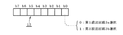
図9は、選択回路4へ入力される選択信号Sを保持するレジスタ12の内部構成を模式的に示す説明図である。図9の例では、レジスタ12は、8ビットレジスタとして構成され、最下位ビットb0に、選択信号Sが保持される。
【0052】
<B.2. 実施の形態2>
図10は、実施の形態2の半導体装置の構成を示すブロック図である。この装置102は、CPU11が配設されず、半導体メモリを制御するためのアドレス信号A、イネーブル信号E、および、選択信号Sが、装置の外部から入力される点において、実施の形態1の装置101とは特徴的に異なっている。
【0053】
装置101には、外部装置を接続することが可能な外部端子30〜33が、さらに備わっている。アドレス信号Aを伝達するアドレスバス6は、外部端子30に接続されている。また、選択信号Sおよびイネーブル信号Eを伝達する信号線は、それぞれ、外部端子31,32に接続されている。また、データ信号を伝達するデータバス5は、外部端子33へ接続されている。
【0054】
CPU11を備えない装置102においても、外部から選択信号Sを入力することによって、装置102の用途、または、動作期間に応じて、第1および第2読出回路3a,3bのいずれかを選択的に使用することが可能である。それによって、高速動作と低消費電流とを、選択自在に達成することができる。
【0055】
<B.3. 実施の形態3>
図11は、実施の形態3の半導体装置の構成の一部を示すブロック図である。図11は、図2との相違点を明瞭にするために、図2と同一部分の図示を省略している。この装置103は、分周器37およびコンパレータ36が、さらに備わっている点において、実施の形態1の装置101とは、特徴的に異なっている。そして、選択信号Sは、CPU11から直接に出力されるのではなく、コンパレータ36を通じて出力される。
【0056】
分周器37は、複数段に縦属接続された単位分周器38を備えている。各単位分周器38は、反復的に入力されるパルスを分周することにより、その周期を二倍に拡張する。装置103には、さらに、外部クロック信号EClkを外部から入力するための外部端子39が備わっている。外部クロック信号EClkは、外部端子39を通じて、分周器37の中の最前段の単位分周器38へ入力される。その結果、分周器37の内部では、外部クロック信号EClkを、2倍、4倍、・・・、32倍に分周して得られる複数の周期を持つパルスが生成される。
【0057】
CPU11には、レジスタ35が備わっている。分周器37は、レジスタ35に保持されるレジスタ値Vにもとづいて、複数のパルスの中から一つを選択し、クロック信号ClkとしてCPU11へ伝達する。CPU11は、このクロック信号Clkに同期して動作する。したがって、CPU11によって制御される半導体メモリも、クロック信号Clkに同期して動作する。
【0058】
コンパレータ36は、レジスタ値Vを基準値と比較し、その結果に応じて、選択信号Sの値を決定する。例えば、レジスタ値Vが基準値よりも小さく、その結果、分周比の低い(したがって、周波数の高い)クロック信号Clkが得られるときには、第1読出回路3aを選択するように、選択信号Sの値が決定される。逆に、レジスタ値Vが基準値以上であって、その結果、分周比の高い(したがって、周波数の低い)クロック信号Clkが得られるときには、第2読出回路3bを選択するように、選択信号Sの値が決定される。
【0059】
このように、装置103では、クロック信号Clkの外部クロック信号EClkに対する分周比の大きさに応じて、第1および第2読出回路3a,3bの間の切替が行われる。すなわち、CPU11が同期するクロック信号Clkの周波数に応じて、第1および第2読出回路3a,3bの間での適切な使い分けが、自動的に行われる。
【0060】
また、CPU11は、その動作を規定するプログラムにもとづいて、レジスタ値Vを書き換えることが可能である。したがって、プログラムの種類、または、一つのプログラムの中での様々な動作期間ごとに、必要に応じて、CPU11の動作速度を変えることが可能である。さらに、CPU11の動作速度の変化に応じて、選択信号Sの設定が、コンパレータ36によって行われるので、プログラムの中で、第1および第2読出回路3a,3bの間の使い分けについては、指示を行う必要がない。
【0061】
図12は、レジスタ35の構造を模式的に示す説明図である。この例では、レジスタ35は、8ビットレジスタとして構成され、最下位3ビットb0〜b2に、レジスタ値Vが保持される。そして、レジスタ値Vの値が1ずつ大きくなるのにともない、分周比が2倍ずつ高くなるように、レジスタ値Vと分周比との関係が設定されている。
【0062】
図13は、コンパレータ36の内部構成の一例を示す回路図である。この例は、レジスタ値Vと分周比との関係が、図12が示すように設定されていることを、前提としている。コンパレータ36は、ビットb0とビットb1の論理積を出力するAND回路40と、AND回路40の出力とビットb2との論理和を、選択信号Sとして出力するOR回路41とを、備えている。
【0063】
したがって、レジスタ値Vが、2進数で"011"以上であるときには、選択信号Sとしてハイレベルが出力され、"010"以下であるときには、ロウレベルが出力される。その結果、分周比が4分周以下であるときには、第1読出回路3aが選択され、分周比が8分周以上であるときには、第2読出回路3bが選択される。
【0064】
<B.4. 実施の形態4>
図14は、実施の形態4の半導体装置の構成の一部を示すブロック図である。図14は、図2と同一部分の図示を省略している。この装置104は、コンパレータが参照する基準値が、外部から入力可能なように構成される点において、実施の形態3の装置103とは、特徴的に異なっている。すなわち、装置104には、コンパレータ36の代わりに、コンパレータ36aが備わっており、基準値を表現する基準信号REを、コンパレータ36aへと伝えるための外部端子45および信号線46が、さらに備わっている。
【0065】
図15が示すように、コンパレータ36aには、例えば、3ビット幅のレジスタ値Vが、レジスタ35から入力されると同時に、それと同一幅の基準信号REが、外部端子45を通じて入力される。コンパレータ36aは、双方の値を比較し、レジスタ値Vが基準信号REよりも大きいか否かに応じて、選択信号Sの値を決定する。
【0066】
このように、装置104では、第1および第2読出回路3a,3bの間で使い分けを行うための分周比の基準値が、外部装置によって設定可能である。このため、外部クロック信号EClkの周波数に応じて、適切な基準値を設定することが可能である。すなわち、分周比だけでなく、外部クロック信号EClkの周波数が変わっても、それに応じた適切な第1および第2読出回路3a,3bの間の使い分けを行うことができる。
【0067】
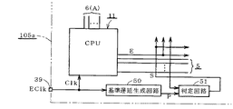
<B.5. 実施の形態5>
図16は、実施の形態5の半導体装置の構成の一部を示すブロック図である。図16は、図2と同一部分の図示を省略している。この装置105は、コンパレータ36の代わりに、基準遅延生成回路50および判定回路51が設置されている点において、実施の形態3の装置103とは、特徴的に異なっている。基準遅延生成回路50は、クロック信号Clkの立ち上がりエッジ(または、立ち下がりエッジ)で定義される1クロック周期の開始時期から、一定時間遅れた遅延時間を表現する基準遅延パルス信号Pを生成する。基準遅延生成回路50は、例えば、クロック信号Clkの立ち上がりエッジに同期して、一定パルス幅のパルスを生成する、従来周知のワンショットパルス生成回路によって構成される。
【0068】
判定回路51は、基準遅延パルス信号Pと、読出回路3の読み出し動作の開始を指示するイネーブル信号Eとを比較し、それにもとづいて選択信号Sを出力する回路であり、例えば、図17の回路図に示すように構成される。この例では、イネーブル信号Eをセット入力信号とするSRラッチ60、基準遅延パルス信号Pをセット入力とするSRラッチ61、SRラッチ60の出力を一方入力に受信するNAND回路66,および、NAND回路66の出力とSRラッチ61の出力とを二入力とするNAND回路67を備えている。SRラッチ60はNAND回路62,63を有しており、SRラッチ61はNAND回路64,65を有している。NAND回路67の出力は、選択信号Sとして選択回路4へ伝えられるとともに、NAND回路66の他方入力へ入力される。
【0069】
図18は、基準遅延生成回路50、判定回路51、および、選択回路4の動作を説明するタイミングチャートである。この例では、基準遅延生成回路50は、クロック信号Clkの立ち上がりから一定の遅延時間Tpを表現する基準遅延パルス信号Pを生成する。基準遅延パルス信号Pのロウレベルで表現される遅延時間Tpは、クロック信号Clkの周期が、長い周期T1であっても、短い周期T2であっても、不変である。
【0070】
イネーブル信号Eは、クロック信号Clkに同期して出力される。判定回路51は、基準遅延パルス信号Pとイネーブル信号Eとが立ち下がるときに、選択信号Sをロウレベルへとリセットする。判定回路51は、さらに、イネーブル信号Eがハイレベルに立ち上がったときの基準遅延パルス信号Pを読み取り、そのレベルに応じて、選択信号Sのレベルを設定する。
【0071】
クロック信号Clkが長い周期T1を持つときには、イネーブル信号Eを読み取る時期は、遅延時間Tpをすでに経過している。このため、読み取られるレベルP1は、ハイレベルとなる。このとき、判定回路51は、選択信号Sを、ハイレベルに設定する。したがって、イネーブル信号Eがハイレベル(アクティブ)となったときに、制御信号Cbがハイレベル(アクティブ)となり、制御信号Caはロウレベル(ノーマル)を維持する。その結果、第1および第2読出回路3a,3bの中で、第2読出回路3bのみが動作する。
【0072】
一方、クロック信号Clkが短い周期T2を持つときには、イネーブル信号Eを読み取る時期は、遅延時間Tpの範囲内にある。このため、読み取られるレベルP2は、ロウレベルとなる。このとき、判定回路51は、選択信号Sを、ロウレベルのままにとどめる。したがって、イネーブル信号Eがハイレベル(アクティブ)となったときに、制御信号Caがハイレベル(アクティブ)となり、制御信号Cbはロウレベル(ノーマル)を維持する。その結果、第1および第2読出回路3a,3bの中で、第1読出回路3aのみが動作する。
【0073】
このように、装置105では、クロック信号Clkの外部クロック信号EClkに対する分周比ではなく、クロック信号Clkそれ自体の周期が、一定の基準値と比較され、その結果に応じて、第1および第2読出回路3a,3bの間での選択が行われる。このため、クロック信号Clkが、分周比の変化だけでなく、外部クロック信号EClkの周波数の変化に由来して、変化した場合においても、常に、クロック信号Clkの周波数に応じた適切な選択が、第1および第2読出回路3a,3bの間で行われる。
【0074】
図17は、外部クロック信号EClkを分周してクロック信号ClkとしてCPU11へ供給する分周器37が備わる装置例を示したが、図19が示すように、分周器37が備わらず、外部端子39を通じて入力される外部クロック信号EClkが、クロック信号Clkとして、直接にCPU11へ供給されてもよい。この装置105aにおいても、基準遅延生成回路50には、クロック信号Clkが入力される。したがって、装置105と同様に、クロック信号Clkの周波数に応じた適切な選択が、第1および第2読出回路3a,3bの間で行われる。
【0075】
<B.6. 実施の形態6>
図20は、実施の形態6の半導体装置の構成を示すブロック図である。この装置106は、並列接続された特性の異なる二つの書込回路72a,72bを備えた書込回路72が設けられた点において、実施の形態1の装置101とは、特徴的に異なっている。読出回路3は、実施の形態1〜5のように、特性の異なる第1および第2読出回路3a,3bを備えてもよいし、また、単一の読出回路のみを備えてもよい。
【0076】
図20には、m個のメモリセルアレイ1の中の一部のみが、代表として示されているが、装置106では、選択回路71と書込回路72の組が、メモリセルアレイ1ごとに設けられている。そして、m個の書込回路72は、データバス5を構成するデータ線D0〜Dmへ、一対一で接続されている。
【0077】
書込回路72は、それが接続されるデータ線(例えば、データ線D0)が伝達するデータ信号を、イネーブル信号Ewに同期して、指定されたメモリセル70へ書き込むための回路である。選択回路71は、第1および第2書込回路72a,72bの双方が出力するデータ信号のいずれかを、選択信号Swにもとづいて選択し、メモリセルアレイ1に備わるすべてのメモリセル70へと伝達する。CPU11には、レジスタ73が備わっており、選択信号Swは、このレジスタ73に保持されている。イネーブル信号Ewも、CPU11から出力される。
【0078】
図21は、第1書込回路72a、第2書込回路72b、および、メモリセル70の内部構成を示す回路図である。メモリセル70は、互いに直列に接続された記憶素子75およびトランスファーゲート76を備えている。記憶素子75は、例えば、ゲート絶縁層に強誘電体を有するMOSトランジスタである。その一方主電極は接地電位線に接続され、ゲート電極は、選択回路71の出力信号を伝達する信号線に接続されている。また、トランスファーゲート76の一方主電極は、ビット線B1〜Bkの一つ(例えば、ビット線Bi)に接続され、そのゲート電極は、ワード線W1〜Wnの一つ(例えば、ワード線Wj)に接続されている。
【0079】
第1書込回路72aは、互いに縦属接続されたインバータ81、インバータ82、および、トランスファーゲート80を備えている。インバータ81の入力は、例えばデータ線D0へ接続され、トランスファーゲート80の一方主電極は、選択回路71の一方入力へ接続されている。また、トランスファーゲート80のゲート電極には、イネーブル信号Ewを伝える信号線が接続されている。
【0080】
第2書込回路72bでは、キャパシタ83と抵抗素子84とを有する積分回路と、トランスファーゲート80とが、縦属接続されている。積分回路の入力は、例えばデータ線D0へ接続され、トランスファーゲート80の一方主電極は、選択回路71の他方入力へ接続されている。トランスファーゲート80のゲート電極には、第1書込回路72aのトランスファーゲート80と同様に、イネーブル信号Ewが入力される。選択回路71は、例えば、従来周知の二入力型のセレクタで構成される。
【0081】
つぎに、図20および図21を参照しつつ、書き込み動作について説明する。メモリセル70にデータ信号を書き込むときには、CPU11は、まず、アドレス信号Aをアドレスバス6へ出力する。ワード線デコーダ7は、アドレス信号Aをデコードすることにより、複数のワード線W1〜Wnの中で、アドレス信号Aが割り当てられたメモリセル、すなわち、書き込みの対象とされるメモリセルが接続されるワード線(例えば、ワード線Wj)を駆動する。
【0082】
それと同時に、ビット線セレクタ8は、アドレス信号Aをデコードすることにより、ビット線B1〜Bkの中で、アドレス信号Aが割り当てられたメモリセルが接続されるビット線(例えば、ビット線Bi)を駆動する。その結果、ワード線Wjとビット線Biとに接続されるトランスファーゲート76がオンする。
【0083】
CPU11は、その後、イネーブル信号Eをアクティブ(図21の例では、ハイレベル)にする。その結果、例えばデータ線D0が伝達するデータ信号が、第1および第2書込回路72a,72bの双方を通じて、選択回路71の二入力へと入力される。選択回路71は、レジスタ73に保持される選択信号Swにもとづいて、第1および第2書込回路72a,72bの出力のいずれかを選択し、メモリセルアレイ1に属するすべての記憶素子75のゲート電極へ伝達する。
【0084】
メモリセルアレイ1に属する複数のメモリセル70の中で、アドレス信号Aで指定された一つ、すなわち、トランスファーゲート76がオンしている一つに限って、その記憶素子75の一対の主電極間に電圧が印加されているため、その記憶素子75にのみ、選択回路71が出力するデータ信号が書き込まれる。その後、イネーブル信号Ewが、ノーマルへと復帰することにより、書き込み動作が終了する。
【0085】
以上の書き込み動作において、第1および第2書込回路72a,72bのそれぞれが出力するデータ信号の波形は、図22の波形図によって描かれる。データ線(例えば、データ線D0)を通じて、第1および第2書込回路72a,72bへ入力されるデータ信号(図22の最上段の曲線)が、あるパルス幅を有する矩形パルスであれば、第1書込回路72aの出力信号は、同様の矩形パルスとなる。これに対して、第2書込回路72bの出力信号は、矩形パルスに緩やかに追随して立ち上がるパルスとなる。
【0086】
すなわち、第1書込回路72aの出力信号は、立ち上がりが急峻であるのに対し、第2書込回路72bの出力信号は、立ち上がりが緩やかである。言い換えると、第1書込回路72aは高速に動作し、第2書込回路72bは緩やかに動作する。
【0087】
メモリセル70は、書き込みおよび消去を反復的に受けることにより、経時的に劣化する場合がある。特に、メモリセル70が、図21に例示するような不揮発性のメモリセルである場合には、劣化が早く、書き込み可能な回数には制限がある。そして、メモリセル70が被る損傷は、印加されるパルス状のデータ信号の立ち上がりが急峻なほど、大きいことが知られている。
【0088】
装置106では、書込回路72として、動作速度が高く、高速書き込みを可能にする第1書込回路72aと、動作速度が低く、メモリセル70の損傷を少なくする第2書込回路72bとが、備わっており、選択回路71によって選択自在に、双方の出力の一方のみが、メモリセルアレイ1へと伝えられる。このため、高速書き込みを必要とする用途または動作期間には、高速書き込みを可能にし、そうでない用途または動作期間には、不必要な高速動作を抑え、メモリセル70の損傷を抑えることができる。
【0089】
特に、装置106では、選択信号Swが、CPU11に備わるレジスタ73の内容によって決定されるので、CPU11の動作を規定するプログラムによって、第1および第2書込回路72a,72bの間の切替を行うことが可能である。また、選択信号Swを決定する形態に関して、実施の形態2〜5と同様に、外部から入力する形態、クロック信号Clkの分周率にもとづいて決定する形態、および、クロック信号Clkの周期それ自体にもとづいて決定する形態、などを採ることも可能である。さらに、実施の形態1〜5と、実施の形態6とを組み合わせて、読出回路3と書込回路72の双方に関して、二つの回路が並列に接続された形態を採ることも可能である。
【0090】
さらに、装置106では、第1および第2書込回路72a,72bの双方が動作し、それら出力するデータ信号が、選択回路71によって選択されて、メモリセルアレイ1へと伝えられたが、選択回路71によって、第1および第2書込回路72a,72bの一方のみが動作するように、装置106を変形することも可能である。それによって、無用な消費電力を節減することが可能となる。装置106とその変形のいずれの形態においても、第1および第2書込回路72a,72bは、メモリセルアレイ1の中で、アドレス信号Aによって指定された特定のメモリセル70へ、排他的に(すなわち、一方のみが選択的に)データ信号を書き込むように動作する。
【0091】
<B.7. 変形例>
実施の形態1〜5では、第1および第2読出回路3a,3bの双方へ、共通のメモリセルの保持信号が入力される例を示した。しかしながら、図23のブロック図が示すように、アドレスが共通で別個のメモリセルの保持信号が、第1および第2読出回路3a,3bへ、個別に入力されるように、装置を構成することも可能である。
【0092】
この装置107では、メモリセルアレイ1には、アドレスを共通にする第1メモリセルアレイ1aおよび第2メモリセルアレイ1bが備わっている。ビット線セレクタ8には、第1メモリセルアレイ1aのビット線Bを選択する第1ビット線セレクタ8aと、第2メモリセルアレイ1bのビット線Bを選択する第2ビット線セレクタ8bとが備わっている。そして、第1ビット線セレクタ8aには第1読出回路3aが接続され、第2ビット線セレクタ8bには第2読出回路3bが接続されている。第1および第2読出回路3a,3bの双方の出力が、共通のデータ線Dに接続される点は、実施の形態1〜5と同様である。
【0093】
この装置107においても、第1および第2読出回路3a,3bのいずれかが、選択回路4によって、選択的に動作するので、消費電力を低減することができる。また、装置107では、第1メモリセルアレイ1aを高速動作に優れ、第2メモリセルアレイ1bを低消費電力に優れるように、構成することにより、高速性を必要としない場合の消費電力を、さらに節減することが可能となる。
【0094】
第1および第2ビット線セレクタ8a,8bの間でも、同様に特性を異ならせることによって、消費電力を一層節減することが可能となる。これに対して、実施の形態1〜5の各装置では、メモリセルアレイ1の半導体チップに占める面積を、装置107に比べて、約半分にまで小さく抑えることができるという、利点がある。
【0095】
【発明の効果】
第1の発明の装置では、動作速度が高い第1読出回路と消費電力が低い第2読出回路とが設けられ、排他的に(すなわち、いずれか一方のみが選択的に)動作するという、特開平5-81865号公報、および、特開平6-275081号公報のいずれにも開示のない特徴が備わる。このため、読み出し動作の高速性が要求されるときには、高速動作を実現し、高速動作が無用であるときには、不必要な消費電力を抑えることができる。すなわち、高速性と低消費電力とを選択自在に実現できるという従来技術にない効果が得られる。また、読み出し速度への要求が異なる様々な用途へ、単一の装置で対応することができる。更にクロック信号の分周比が基準値に対して大きいときには、低消費電力を実現する読出回路が動作し、逆に、小さいときには、高速動作を実現する読出回路が動作する。すなわち、分周比に応じて、適切な動作が自動的に実現する。
【0096】
第2の発明の装置では、CPUに備わるレジスタに保持される信号にもとづいて選択的に、第1および第2読出回路が動作するので、CPUの動作を規定するプログラム(ソフトウェア)によって、高速動作と低消費電力動作との間の切替を行うことができる。
【0098】
第3の発明の装置では、基準値が外部入力によって可変であるため、分周比だけでなく、外部クロック信号の周波数を変えたときにも、それに応じて、第1および第2読出回路の間で、適切な切替え動作を行うことができる。
【0099】
第4の発明の装置では、CPUがメモリセルアレイへのアクセスを開始する時期が、クロック信号の1クロック周期の開始から一定時間後までの遅延時間以内であるときには、高速動作を実現する読出回路が動作し、逆に、遅延時間以内でないときには、低消費電力を実現する読出回路が動作する。このため、CPUのクロック信号の周波数が変わっても、周波数に応じた適切な動作が自動的に実現する。
【0100】
第5の発明の装置では、第1および第2読出回路が保持信号のレベルを判別する対象とするメモリセルが、互いに同一のメモリセルであるので、互いにアドレスのみを共通にする別個のメモリセルを対象とする形態に比べて、メモリセルアレイが占める面積が、約半分に節減される。
【図面の簡単な説明】
【図1】 各実施の形態の概略を示すブロック図である。
【図2】 実施の形態1の装置のブロック図である。
【図3】 図2の第1読出回路のブロック図である。
【図4】 図3のセンスアンプの回路図である。
【図5】 図3のセンスアンプの別の例の回路図である。
【図6】 図3のバッファの回路図である。
【図7】 図2の第2読出回路のブロック図である。
【図8】 図2の選択回路の回路図である。
【図9】 図2のレジスタの構成を示す説明図である。
【図10】 実施の形態2の装置のブロック図である。
【図11】 実施の形態3の装置のブロック図である。
【図12】 図11のレジスタの構成を示す説明図である。
【図13】 図11のコンパレータの回路図である。
【図14】 実施の形態4の装置のブロック図である。
【図15】 図14のコンパレータの動作を示す説明図である。
【図16】 実施の形態5の装置のブロック図である。
【図17】 図16の判定回路の回路図である。
【図18】 図16の装置の動作を示すタイミングチャートである。
【図19】 実施の形態5の装置の変形例を示すブロック図である。
【図20】 実施の形態6の装置のブロック図である。
【図21】 図20の書込回路とメモリセルの構成を示す回路図である。
【図22】 図21の書込回路の動作を示す波形図である。
【図23】 変形例の装置のブロック図である。
【図24】 従来の装置のブロック図である。
【符号の説明】
1 メモリセルアレイ、3a 第1読出回路、3b 第2読出回路、4 選択回路、11 CPU、12 レジスタ、36 コンパレータ、37 分周器、45外部端子、50 基準遅延生成回路、51 判定回路、70 メモリセル、71 選択回路、72a 第1書込回路、72b 第2書込回路、A アドレス信号、Clk クロック信号、E イネーブル信号、Ew イネーブル信号、EClk 外部クロック信号、I0 保持信号、RE 基準信号、S 選択信号、Sw 選択信号、P 基準遅延パルス信号。[0001]
BACKGROUND OF THE INVENTION
The present invention relates to a semiconductor device including a memory cell array, and more particularly to an improvement for reducing power consumption or memory cell wear.
[0002]
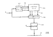
[Prior art]
FIG. 24 is a block diagram showing a schematic configuration of a conventional semiconductor device including a semiconductor memory. The
[0003]
When the data held in the memory cell is read, the
[0004]
As a result, the holding signals of the plurality of memory cells connected to the driven word line are output to the
[0005]
[Problems to be solved by the invention]
By the way, in recent years, an MCU (microcontroller or microcomputer) in which a CPU and a peripheral circuit including a semiconductor memory are incorporated in a single semiconductor chip is required to have higher speed and to the environment. From the viewpoint of consideration of the above, it is required to operate with lower power consumption. In terms of high-speed performance, the operation speed of the readout circuit of the semiconductor memory is usually governed by the speed of the entire MCU, and the power consumption of the semiconductor memory also accounts for the majority of the power consumption of the entire MCU. ing.
[0006]
However, high speed and low power consumption are technically conflicting requirements, and it is not easy to satisfy both of them simultaneously. Therefore, an MCU user who manufactures a product using an MCU usually uses a high-speed MCU and a low-power consumption MCU properly according to each purpose. However, depending on the product manufactured by the user, there may be an application in which an operation period in which high speed is prioritized and an operation period in which high speed is unnecessary and low power consumption is prioritized are mixed. Even in such applications, it is necessary to use an MCU capable of high-speed operation, resulting in unnecessary power consumption.
[0007]
In such applications, to reduce power consumption as much as possible, use a MCU with excellent high-speed performance, and when low power consumption is a priority, use the CPU's CPU halt mode or wait mode. Even if you suppress the unnecessary operation of the MCU or change the frequency division ratio of the external clock signal supplied from the outside to the MCU, the frequency of the clock signal that the CPU synchronizes (ie, the internal clock signal) can be kept low. , Was taken.
[0008]
However, in an MCU capable of high-speed operation, a current mirror circuit that is a current-driven type with high power consumption is used for its readout circuit. In the current mirror circuit, since the current that flows steadily is large, there is no significant change in power consumption even if the internal clock is slowed down and the operation speed is slowed down. Therefore, there is a problem that the power consumption of the MCU is not effectively saved.
[0009]
In the above description, an MCU is used as an example. However, in general semiconductor devices equipped with a semiconductor memory, not limited to an MCU, the characteristics of a readout circuit are less demanding to prioritize high speed depending on the application and operation period. There has been a demand for a semiconductor device that can flexibly meet demands for prioritizing power consumption.
[0010]
Further, in the nonvolatile semiconductor memory, there is a problem that if the operation speed of the writing circuit that is paired with the reading circuit is unnecessarily increased, the wear of the memory cell that holds data is accelerated. For this reason, it is desired that the characteristics of the write circuit can flexibly respond to the request that prioritizes high speed and the request that prioritizes protection of the memory cell according to the use and operation period of the semiconductor device. It was.
[0011]
The present invention has been made to solve the above-described problems in the conventional apparatus, and the characteristics of the read circuit or the write circuit can flexibly correspond to the priority of the operation speed requirement, thereby An object of the present invention is to obtain a semiconductor device capable of reducing power or wear of a memory cell.
[0012]
Note that Japanese Patent Laid-Open Nos. 5-81865 and 6-275081 are known as documents that simply disclose a configuration in which a plurality of readout circuits are connected to a common data line.
[0013]
[Means for Solving the Problems]
According to a first aspect of the present invention, there is provided a semiconductor device including a memory cell array having a plurality of memory cells, and a first readout circuit that reads and outputs a signal held by a specified one of the plurality of memory cells. And reading and outputting a signal held by a designated one of the plurality of memory cells, and having a lower operating speed and lower power consumption than the first reading circuit, and the first reading circuit A second readout circuit that operates exclusively.Furthermore, it operates in synchronization with the clock signal and accesses the memory cell array. CPU And dividing the external clock signal input from the outside in a plurality of ways, generating a signal having a plurality of periods, and selecting one of them as the clock signal CPU And a comparator that compares a frequency division ratio of the clock signal to the external clock signal with a reference value. In the comparison result of the comparator, when the frequency division ratio is large with the reference value as a boundary, only the second read circuit operates among the first and second read circuits, and conversely, when the frequency division ratio is small, the first read circuit Only the readout circuit operates.
[0014]
A device according to a second aspect of the present invention is the semiconductor device according to the first aspect, further comprising a CPU that accesses the memory cell array, wherein the CPU includes a register, and the first and second readout circuits are configured as described above. It operates exclusively based on the signal held in the register.
[0016]
First3The device of the invention1The semiconductor device according to the present invention further includes an external terminal, and the comparator uses a value expressed by a signal input from the external terminal as the reference value.
[0017]
First4The device of the invention ofA semiconductor device, a memory cell array having a plurality of memory cells, a first read circuit for reading and outputting a signal held by a specified one of the plurality of memory cells, and a plurality of memory cells Among them, the signal held by the designated one is read and output, and the second read operation is slower than the first read circuit and consumes less power and operates exclusively with the first read circuit. A circuit. Furthermore,The CPU operates in synchronization with the clock signal, and generates a pulse representing the delay time from the start of one clock cycle of the clock signal to a certain time later, for each CPU cycle, accessing the memory cell array. A reference delay generation circuit and a determination circuit for determining whether or not the time when the CPU instructs the start of the operation of the first or second readout circuit is within the delay timeAndPreparationTheIn the determination result of the determination circuit, when the time is within the delay time, only the first read circuit operates in the first and second read circuits. Only the readout circuit operates.
[0018]
First5In the apparatus of the invention, the first to the first4In the semiconductor device of any one of the above, the memory cells to be read by the first and second readout circuits are the same memory cells.
[0020]
DETAILED DESCRIPTION OF THE INVENTION
<A. Outline of the embodiment>
FIG. 1 is a block diagram showing an outline of an embodiment of the present invention. The
[0021]
When the data held in the memory cell is read, the
[0022]
As a result, the holding signals of the plurality of memory cells connected to the driven word line are output to the bit line selector 8 through the plurality of bit lines B, respectively. The bit line selector 8 selects one of the plurality of bit lines B to which the designated memory cell is connected, and transmits the hold signal to the
[0023]
As described above, the data held in the specified specific memory cell is read out. In order to enable simultaneous reading of data of a plurality of bits (that is, parallel reading), a plurality of sets of the
[0024]
The
[0025]
The selection circuit 4 selectively operates (that is, exclusively) one of the first and
[0026]
In the
[0027]
Similarly, not only the reading circuit but also the writing circuit (not shown) can include a writing circuit having a plurality of characteristics and can be operated selectively (that is, exclusively). Thereby, it is possible to suppress the wear of the memory cell. This form will be described in
[0028]
In addition, the memory cells to be read by each of the first and
[0029]
<B.1.
First, the first embodiment will be described.
[0030]
<B.1.1. Overall configuration of the device>
FIG. 2 is a block diagram showing a configuration of the semiconductor device of the first embodiment. In this device 101, a
[0031]
In the device 101, the memory
[0032]
Instead of providing the selection circuit 4 for each
[0033]
The
[0034]
As a result, in each of the m
[0035]
The
[0036]
When one of the control signals Ca and Cb becomes active, only one of the first and
[0037]
As described above, in the device 101, since the selection signal S is determined by the contents of the
[0038]
In general, application programs used by the user of the apparatus 101 can be those that require high-speed operation and those that do not. Even in the same program, there can be a period in which high-speed operation is required and a period in which it is not required in the operation period. The apparatus 101 selectively realizes high-speed operation and power consumption saving according to the contents of such application programs.
[0039]
<B.1.2. Read circuit>
Next, the internal configuration of the
[0040]
In response to the active control signal Ca, the
[0041]
FIG. 4 is a circuit diagram showing an example of the internal configuration of the
[0042]
The non-inverted signal IN is input to the gate electrode of the
[0043]
When the control signal Ca is normal, the
[0044]
FIG. 5 is a circuit diagram showing another example of the internal configuration of the
[0045]
The holding signal I 0 is input to the gate electrode of the
[0046]
When an active signal is input as the control signal Ca and the differential amplifier enters an operating state, a high level or low level output obtained by amplifying the difference between the holding signal I0 and the reference potential Ref from the drain electrode of the
[0047]
FIG. 6 is a circuit diagram showing the internal configuration of the
[0048]
FIG. 7 is a block diagram showing an example of the internal configuration of the
[0049]
<B.1.3. Selection circuit>
FIG. 8 is a circuit diagram showing an example of the internal configuration of the selection circuit 4. The selection circuit 4 includes AND
[0050]
As a result, the AND
[0051]
FIG. 9 is an explanatory diagram schematically showing the internal configuration of the
[0052]
<B.2.
FIG. 10 is a block diagram showing a configuration of the semiconductor device of the second embodiment. The
[0053]
The device 101 further includes
[0054]
Even in the
[0055]
<B.3. Third Embodiment>
FIG. 11 is a block diagram illustrating a part of the configuration of the semiconductor device according to the third embodiment. FIG. 11 omits the same parts as those in FIG. 2 in order to clarify the differences from FIG.
[0056]
The
[0057]
The
[0058]
The
[0059]
Thus, in the
[0060]
Further, the
[0061]
FIG. 12 is an explanatory diagram schematically showing the structure of the
[0062]
FIG. 13 is a circuit diagram showing an example of the internal configuration of the
[0063]
Accordingly, when the register value V is “011” or higher in binary, a high level is output as the selection signal S, and when it is “010” or lower, a low level is output. As a result, when the division ratio is 4 or less, the
[0064]
<B.4. Embodiment 4>
FIG. 14 is a block diagram showing a part of the configuration of the semiconductor device of the fourth embodiment. In FIG. 14, the same parts as those in FIG. 2 are not shown. This
[0065]
As shown in FIG. 15, for example, a register value V having a 3-bit width is input to the
[0066]
As described above, in the
[0067]
<B.5.
FIG. 16 is a block diagram illustrating a part of the configuration of the semiconductor device according to the fifth embodiment. In FIG. 16, the same parts as those in FIG. 2 are not shown. This
[0068]
The
[0069]
FIG. 18 is a timing chart for explaining operations of the reference
[0070]
The enable signal E is output in synchronization with the clock signal Clk. The
[0071]
When the clock signal Clk has a long period T1, the delay time Tp has already passed when the enable signal E is read. For this reason, the read level P1 becomes a high level. At this time, the
[0072]
On the other hand, when the clock signal Clk has a short period T2, the timing for reading the enable signal E is within the range of the delay time Tp. Therefore, the level P2 to be read is a low level. At this time, the
[0073]
In this way, the
[0074]
FIG. 17 shows an example of a device provided with a
[0075]
<B.6.
FIG. 20 is a block diagram showing a configuration of the semiconductor device of the sixth embodiment. This
[0076]
In FIG. 20, only a part of the m
[0077]
The
[0078]
FIG. 21 is a circuit diagram showing the internal configuration of
[0079]
The
[0080]
In the
[0081]
Next, the write operation will be described with reference to FIG. 20 and FIG. When writing a data signal to the
[0082]
At the same time, the bit line selector 8 decodes the address signal A, so that the bit line (for example, bit line Bi) to which the memory cell to which the address signal A is assigned is connected among the bit lines B1 to Bk. To drive. As a result, the
[0083]
Thereafter, the
[0084]
Of the plurality of
[0085]
In the above write operation, the waveform of the data signal output from each of the first and
[0086]
That is, the output signal of the
[0087]
The
[0088]
In the
[0089]
In particular, in the
[0090]
Further, in the
[0091]
<B.7. Modification>
In the first to fifth embodiments, the example in which the common memory cell holding signal is input to both the first and
[0092]
In this
[0093]
Also in this
[0094]
By similarly changing the characteristics between the first and second
[0095]
【The invention's effect】
The device of the first invention is provided with a first readout circuit having a high operating speed and a second readout circuit having a low power consumption, and operates exclusively (that is, only one of them selectively). Neither Kaihei 5-81865 nor Japanese Patent Laid-Open No. 6-275081 has features that are not disclosed. For this reason, high speed operation is realized when high speed read operation is required, and unnecessary power consumption can be suppressed when high speed operation is unnecessary. That is, there is an effect that is not available in the prior art in that high speed and low power consumption can be freely selected. In addition, it is possible to cope with various uses having different requirements for the reading speed with a single device.Further, when the frequency division ratio of the clock signal is large with respect to the reference value, the read circuit that realizes low power consumption operates. That is, an appropriate operation is automatically realized according to the frequency division ratio.
[0096]
In the device according to the second aspect of the invention, the first and second readout circuits are selectively operated based on signals held in a register provided in the CPU, so that a high-speed operation is performed by a program (software) that defines the operation of the CPU. And low power consumption operation can be switched.
[0098]
First3In the device of the invention, since the reference value is variable by the external input, not only the frequency division ratio but also the frequency of the external clock signal is changed between the first and second readout circuits accordingly. Therefore, an appropriate switching operation can be performed.
[0099]
First4In the device of the invention, when the timing at which the CPU starts accessing the memory cell array is within the delay time from the start of one clock cycle of the clock signal to a certain time later, the readout circuit that realizes high-speed operation operates. On the contrary, when it is not within the delay time, the readout circuit realizing low power consumption operates. For this reason, even if the frequency of the CPU clock signal changes, an appropriate operation corresponding to the frequency is automatically realized.
[0100]
First5In the device of the invention, since the memory cells for which the first and second readout circuits determine the level of the holding signal are the same memory cells, they are intended for separate memory cells that share only an address with each other. Compared with the embodiment, the area occupied by the memory cell array is reduced to about half.
[Brief description of the drawings]
FIG. 1 is a block diagram showing an outline of each embodiment.
FIG. 2 is a block diagram of an apparatus according to the first embodiment.
FIG. 3 is a block diagram of a first read circuit in FIG. 2;
4 is a circuit diagram of the sense amplifier of FIG. 3. FIG.
FIG. 5 is a circuit diagram of another example of the sense amplifier of FIG. 3;
6 is a circuit diagram of the buffer of FIG. 3. FIG.
7 is a block diagram of the second readout circuit of FIG. 2. FIG.
FIG. 8 is a circuit diagram of the selection circuit of FIG. 2;
FIG. 9 is an explanatory diagram showing a configuration of the register of FIG. 2;
FIG. 10 is a block diagram of an apparatus according to a second embodiment.
FIG. 11 is a block diagram of an apparatus according to a third embodiment.
12 is an explanatory diagram showing a configuration of the register of FIG. 11;
13 is a circuit diagram of the comparator in FIG.
FIG. 14 is a block diagram of an apparatus according to a fourth embodiment.
FIG. 15 is an explanatory diagram showing the operation of the comparator of FIG. 14;
FIG. 16 is a block diagram of an apparatus according to a fifth embodiment.
17 is a circuit diagram of the determination circuit in FIG. 16;
18 is a timing chart showing the operation of the apparatus shown in FIG.
FIG. 19 is a block diagram showing a modification of the apparatus according to the fifth embodiment.
FIG. 20 is a block diagram of an apparatus according to a sixth embodiment.
21 is a circuit diagram showing a configuration of a write circuit and a memory cell in FIG. 20;
22 is a waveform diagram showing an operation of the writing circuit of FIG. 21. FIG.
FIG. 23 is a block diagram of a modified apparatus.
FIG. 24 is a block diagram of a conventional apparatus.
[Explanation of symbols]
DESCRIPTION OF
Claims (5)
前記複数のメモリセルの中で、指定されたものが保持する信号を読み出し、出力する第1読出回路と、
前記複数のメモリセルの中で、指定されたものが保持する信号を読み出し、出力するとともに、前記第1読出回路よりも動作速度が遅く消費電力が低く、かつ、前記第1読出回路と排他的に動作する第2読出回路と、
クロック信号に同期して動作するとともに、前記メモリセルアレイにアクセスする CPU と、
外部から入力される外部クロック信号を複数通りに分周し、複数の周期を有する信号を生成するとともに、その中の一つを選択して前記クロック信号として前記 CPU へ供給する分周器と、
前記クロック信号の前記外部クロック信号に対する分周比を基準値と比較するコンパレータとを備え、
前記コンパレータの比較結果において前記分周比が前記基準値を境として大きいときには、前記第1および第2読出回路の中で、前記第2読出回路のみが動作し、逆に小さいときには、前記第1読出回路のみが動作する半導体装置。A memory cell array having a plurality of memory cells;
A first readout circuit for reading out and outputting a signal held by a designated one of the plurality of memory cells;
Reads and outputs a signal held by a designated one of the plurality of memory cells, and has a lower operating speed and lower power consumption than the first reading circuit, and is exclusive to the first reading circuit. A second readout circuit operating in
A CPU that operates in synchronization with the clock signal and accesses the memory cell array ;
A frequency divider that divides the external clock signal inputted from the outside in a plurality of ways, generates a signal having a plurality of cycles, and selects one of them to supply the CPU as the clock signal ;
A comparator that compares a division ratio of the clock signal to the external clock signal with a reference value;
In the comparison result of the comparator, when the frequency division ratio is large with the reference value as a boundary, only the second read circuit operates in the first and second read circuits. the semiconductor device only read circuit that runs.
当該CPUは、レジスタを備えており、
前記第1および第2読出回路は、前記レジスタに保持される信号にもとづいて、排他的に動作する、請求項1に記載の半導体装置。A CPU for accessing the memory cell array;
The CPU has a register,
2. The semiconductor device according to claim 1, wherein the first and second readout circuits operate exclusively based on a signal held in the register.
前記コンパレータは、前記外部端子から入力される信号が表現する値を前記基準値とする、請求項1に記載の半導体装置。 An external terminal is further provided,
The comparator, the you the value signal representing input from the external terminal and the reference value, the semiconductor device according to claim 1.
前記複数のメモリセルの中で、指定されたものが保持する信号を読み出し、出力する第1読出回路と、
前記複数のメモリセルの中で、指定されたものが保持する信号を読み出し、出力するとともに、前記第1読出回路よりも動作速度が遅く消費電力が低く、かつ、前記第1読出回路と排他的に動作する第2読出回路と、
クロック信号に同期して動作するとともに、前記メモリセルアレイにアクセスする CPU と、
前記クロック信号の1クロック周期の開始から一定時間後までの遅延時間を、前記1クロック周期ごとに表現するパルスを生成する基準遅延生成回路と、
前記 CPU が前記第1または第2読出回路の動作開始を指示する時期が、前記遅延時間以内であるか否かを判定する判定回路と
を備え、
前記判定回路の判定結果において前記時期が前記遅延時間以内であるときには、前記第1および第2読出回路の中で、前記第1読出回路のみが動作し、逆に以内でないときには、前記第2読出回路のみが動作する半導体装置。 A memory cell array having a plurality of memory cells;
A first readout circuit for reading out and outputting a signal held by a designated one of the plurality of memory cells;
Reads and outputs a signal held by a designated one of the plurality of memory cells, and has a lower operating speed and lower power consumption than the first reading circuit, and is exclusive to the first reading circuit. A second readout circuit operating in
A CPU that operates in synchronization with the clock signal and accesses the memory cell array ;
A reference delay generation circuit that generates a pulse expressing a delay time from the start of one clock cycle of the clock signal to a certain time later for each one clock cycle;
A determination circuit for determining whether or not a time when the CPU instructs to start the operation of the first or second readout circuit is within the delay time;
With
In the determination result of the determination circuit, when the time is within the delay time, only the first read circuit operates in the first and second read circuits, and conversely, when not within the delay time, the second read A semiconductor device in which only the circuit operates .
Priority Applications (2)
| Application Number | Priority Date | Filing Date | Title |
|---|---|---|---|
| JP03695399A JP4112729B2 (en) | 1999-02-16 | 1999-02-16 | Semiconductor device |
| US09/411,836 US6219300B1 (en) | 1999-02-16 | 1999-10-04 | Semiconductor device |
Applications Claiming Priority (1)
| Application Number | Priority Date | Filing Date | Title |
|---|---|---|---|
| JP03695399A JP4112729B2 (en) | 1999-02-16 | 1999-02-16 | Semiconductor device |
Publications (3)
| Publication Number | Publication Date |
|---|---|
| JP2000235796A JP2000235796A (en) | 2000-08-29 |
| JP2000235796A5 JP2000235796A5 (en) | 2005-10-27 |
| JP4112729B2 true JP4112729B2 (en) | 2008-07-02 |
Family
ID=12484121
Family Applications (1)
| Application Number | Title | Priority Date | Filing Date |
|---|---|---|---|
| JP03695399A Expired - Fee Related JP4112729B2 (en) | 1999-02-16 | 1999-02-16 | Semiconductor device |
Country Status (2)
| Country | Link |
|---|---|
| US (1) | US6219300B1 (en) |
| JP (1) | JP4112729B2 (en) |
Cited By (1)
| Publication number | Priority date | Publication date | Assignee | Title |
|---|---|---|---|---|
| JPH0751920A (en) * | 1993-08-19 | 1995-02-28 | Techno Sakato:Kk | Shaft device and cutter using it |
Families Citing this family (27)
| Publication number | Priority date | Publication date | Assignee | Title |
|---|---|---|---|---|
| JP2001222899A (en) * | 1999-11-30 | 2001-08-17 | Seiko Epson Corp | Semiconductor integrated circuit |
| US20030112665A1 (en) * | 2001-12-17 | 2003-06-19 | Nec Electronics Corporation | Semiconductor memory device, data processor, and method of determining frequency |
| US7106636B2 (en) * | 2004-06-22 | 2006-09-12 | Intel Corporation | Partitionable memory device, system, and method |
| KR100672147B1 (en) * | 2005-03-15 | 2007-01-19 | 주식회사 하이닉스반도체 | Page buffer for preventing program fail in check board program of non-volatile memory device |
| KR100756798B1 (en) | 2006-04-24 | 2007-09-07 | 주식회사 하이닉스반도체 | Radio frequency identification device |
| US7536570B2 (en) * | 2006-10-02 | 2009-05-19 | Silicon Laboratories Inc. | Microcontroller unit (MCU) with suspend mode |
| US7877551B2 (en) * | 2007-06-26 | 2011-01-25 | International Business Machines Corporation | Programmable partitioning for high-performance coherence domains in a multiprocessor system |
| US7802025B2 (en) | 2007-06-26 | 2010-09-21 | International Business Machines Corporation | DMA engine for repeating communication patterns |
| US7984448B2 (en) * | 2007-06-26 | 2011-07-19 | International Business Machines Corporation | Mechanism to support generic collective communication across a variety of programming models |
| US8010875B2 (en) | 2007-06-26 | 2011-08-30 | International Business Machines Corporation | Error correcting code with chip kill capability and power saving enhancement |
| US8108738B2 (en) | 2007-06-26 | 2012-01-31 | International Business Machines Corporation | Data eye monitor method and apparatus |
| US8458282B2 (en) | 2007-06-26 | 2013-06-04 | International Business Machines Corporation | Extended write combining using a write continuation hint flag |
| US8140925B2 (en) | 2007-06-26 | 2012-03-20 | International Business Machines Corporation | Method and apparatus to debug an integrated circuit chip via synchronous clock stop and scan |
| US7793038B2 (en) | 2007-06-26 | 2010-09-07 | International Business Machines Corporation | System and method for programmable bank selection for banked memory subsystems |
| US8509255B2 (en) | 2007-06-26 | 2013-08-13 | International Business Machines Corporation | Hardware packet pacing using a DMA in a parallel computer |
| US7827391B2 (en) | 2007-06-26 | 2010-11-02 | International Business Machines Corporation | Method and apparatus for single-stepping coherence events in a multiprocessor system under software control |
| US8756350B2 (en) | 2007-06-26 | 2014-06-17 | International Business Machines Corporation | Method and apparatus for efficiently tracking queue entries relative to a timestamp |
| US8103832B2 (en) * | 2007-06-26 | 2012-01-24 | International Business Machines Corporation | Method and apparatus of prefetching streams of varying prefetch depth |
| US8468416B2 (en) | 2007-06-26 | 2013-06-18 | International Business Machines Corporation | Combined group ECC protection and subgroup parity protection |
| US7886084B2 (en) | 2007-06-26 | 2011-02-08 | International Business Machines Corporation | Optimized collectives using a DMA on a parallel computer |
| US7873843B2 (en) * | 2007-06-26 | 2011-01-18 | International Business Machines Corporation | Static power reduction for midpoint-terminated busses |
| US8032892B2 (en) * | 2007-06-26 | 2011-10-04 | International Business Machines Corporation | Message passing with a limited number of DMA byte counters |
| US8230433B2 (en) | 2007-06-26 | 2012-07-24 | International Business Machines Corporation | Shared performance monitor in a multiprocessor system |
| EP2539897B1 (en) * | 2010-02-23 | 2020-03-18 | Rambus Inc. | Methods and circuits for dynamically scaling dram power and performance |
| JP5328957B2 (en) * | 2012-04-17 | 2013-10-30 | ルネサスエレクトロニクス株式会社 | Semiconductor memory device |
| TWI610179B (en) * | 2016-12-07 | 2018-01-01 | 慧榮科技股份有限公司 | Host device and methods for controlling a data transfer speed |
| JP2020004119A (en) * | 2018-06-28 | 2020-01-09 | ルネサスエレクトロニクス株式会社 | Semiconductor device and control system using same |
Family Cites Families (5)
| Publication number | Priority date | Publication date | Assignee | Title |
|---|---|---|---|---|
| JP2743653B2 (en) | 1991-09-20 | 1998-04-22 | 富士通株式会社 | Semiconductor storage device |
| JPH06275081A (en) | 1993-03-18 | 1994-09-30 | Fujitsu Ltd | Semiconductor storage |
| US5497355A (en) * | 1994-06-03 | 1996-03-05 | Intel Corporation | Synchronous address latching for memory arrays |
| JPH10275140A (en) * | 1997-03-31 | 1998-10-13 | Nec Ic Microcomput Syst Ltd | Microcomputer |
| JP3090104B2 (en) * | 1997-10-27 | 2000-09-18 | 日本電気株式会社 | Semiconductor memory device |
-
1999
- 1999-02-16 JP JP03695399A patent/JP4112729B2/en not_active Expired - Fee Related
- 1999-10-04 US US09/411,836 patent/US6219300B1/en not_active Expired - Lifetime
Cited By (1)
| Publication number | Priority date | Publication date | Assignee | Title |
|---|---|---|---|---|
| JPH0751920A (en) * | 1993-08-19 | 1995-02-28 | Techno Sakato:Kk | Shaft device and cutter using it |
Also Published As
| Publication number | Publication date |
|---|---|
| US6219300B1 (en) | 2001-04-17 |
| JP2000235796A (en) | 2000-08-29 |
Similar Documents
| Publication | Publication Date | Title |
|---|---|---|
| JP4112729B2 (en) | Semiconductor device | |
| US7227777B2 (en) | Mode selection in a flash memory device | |
| JP5661891B2 (en) | System and method for dynamic power saving in electrical memory operation | |
| TWI404063B (en) | Memory system and control method for memory | |
| US4961172A (en) | Decoder for a memory address bus | |
| JPH10242842A (en) | Microcontroller accessible macrocell | |
| JP2599841B2 (en) | Data processing device | |
| US10529407B2 (en) | Memory device including a plurality of power rails and method of operating the same | |
| JP3754593B2 (en) | Integrated circuit having memory cells for storing data bits and method for writing write data bits to memory cells in integrated circuits | |
| US5623221A (en) | Low noise MOSFET employing selective drive signals | |
| US6937515B2 (en) | Semiconductor memory device | |
| JPS6249676B2 (en) | ||
| JPS58139392A (en) | Semiconductor memory | |
| US6404688B2 (en) | Semiconductor memory device having a self-refresh operation | |
| JPH113596A (en) | A set of paired memories arranged on the same monolithic integrated circuit | |
| US7978547B2 (en) | Data I/O control signal generating circuit in a semiconductor memory apparatus | |
| US6157211A (en) | FPGA using RAM control signal lines as routing or logic resources after configuration | |
| JPH04360095A (en) | Semiconductor memory | |
| US6246633B1 (en) | Semiconductor memory device permitting stabilized operation and high-speed access | |
| JP2937203B2 (en) | Semiconductor memory device | |
| JPS61153895A (en) | Semiconductor memory device | |
| CN113948134A (en) | Storage device and input/output buffer control method thereof | |
| JPH07111834B2 (en) | Serial access memory | |
| JP2002230979A (en) | Semiconductor memory, and its control circuit | |
| JPH04113584A (en) | Semiconductor memory device |
Legal Events
| Date | Code | Title | Description |
|---|---|---|---|
| A521 | Written amendment |
Free format text: JAPANESE INTERMEDIATE CODE: A523 Effective date: 20050707 |
|
| A621 | Written request for application examination |
Free format text: JAPANESE INTERMEDIATE CODE: A621 Effective date: 20050707 |
|
| A131 | Notification of reasons for refusal |
Free format text: JAPANESE INTERMEDIATE CODE: A131 Effective date: 20080108 |
|
| A521 | Written amendment |
Free format text: JAPANESE INTERMEDIATE CODE: A523 Effective date: 20080227 |
|
| RD04 | Notification of resignation of power of attorney |
Free format text: JAPANESE INTERMEDIATE CODE: A7424 Effective date: 20080227 |
|
| TRDD | Decision of grant or rejection written | ||
| A01 | Written decision to grant a patent or to grant a registration (utility model) |
Free format text: JAPANESE INTERMEDIATE CODE: A01 Effective date: 20080408 |
|
| A61 | First payment of annual fees (during grant procedure) |
Free format text: JAPANESE INTERMEDIATE CODE: A61 Effective date: 20080410 |
|
| R150 | Certificate of patent or registration of utility model |
Free format text: JAPANESE INTERMEDIATE CODE: R150 |
|
| FPAY | Renewal fee payment (event date is renewal date of database) |
Free format text: PAYMENT UNTIL: 20110418 Year of fee payment: 3 |
|
| FPAY | Renewal fee payment (event date is renewal date of database) |
Free format text: PAYMENT UNTIL: 20110418 Year of fee payment: 3 |
|
| S111 | Request for change of ownership or part of ownership |
Free format text: JAPANESE INTERMEDIATE CODE: R313111 |
|
| FPAY | Renewal fee payment (event date is renewal date of database) |
Free format text: PAYMENT UNTIL: 20110418 Year of fee payment: 3 |
|
| R350 | Written notification of registration of transfer |
Free format text: JAPANESE INTERMEDIATE CODE: R350 |
|
| FPAY | Renewal fee payment (event date is renewal date of database) |
Free format text: PAYMENT UNTIL: 20120418 Year of fee payment: 4 |
|
| FPAY | Renewal fee payment (event date is renewal date of database) |
Free format text: PAYMENT UNTIL: 20120418 Year of fee payment: 4 |
|
| FPAY | Renewal fee payment (event date is renewal date of database) |
Free format text: PAYMENT UNTIL: 20130418 Year of fee payment: 5 |
|
| FPAY | Renewal fee payment (event date is renewal date of database) |
Free format text: PAYMENT UNTIL: 20140418 Year of fee payment: 6 |
|
| S531 | Written request for registration of change of domicile |
Free format text: JAPANESE INTERMEDIATE CODE: R313531 |
|
| R350 | Written notification of registration of transfer |
Free format text: JAPANESE INTERMEDIATE CODE: R350 |
|
| LAPS | Cancellation because of no payment of annual fees |