JP4112527B2 - Method for manufacturing light emitting device of system on panel type - Google Patents
Method for manufacturing light emitting device of system on panel type Download PDFInfo
- Publication number
- JP4112527B2 JP4112527B2 JP2004185758A JP2004185758A JP4112527B2 JP 4112527 B2 JP4112527 B2 JP 4112527B2 JP 2004185758 A JP2004185758 A JP 2004185758A JP 2004185758 A JP2004185758 A JP 2004185758A JP 4112527 B2 JP4112527 B2 JP 4112527B2
- Authority
- JP
- Japan
- Prior art keywords
- tft
- semiconductor film
- film
- light
- emitting device
- Prior art date
- Legal status (The legal status is an assumption and is not a legal conclusion. Google has not performed a legal analysis and makes no representation as to the accuracy of the status listed.)
- Active
Links
- 238000000034 method Methods 0.000 title claims description 27
- 238000004519 manufacturing process Methods 0.000 title claims description 18
- 239000004065 semiconductor Substances 0.000 claims description 195
- 239000000758 substrate Substances 0.000 claims description 58
- 239000012535 impurity Substances 0.000 claims description 41
- 239000007789 gas Substances 0.000 claims description 26
- XKRFYHLGVUSROY-UHFFFAOYSA-N Argon Chemical compound [Ar] XKRFYHLGVUSROY-UHFFFAOYSA-N 0.000 claims description 14
- 229910021332 silicide Inorganic materials 0.000 claims description 12
- FVBUAEGBCNSCDD-UHFFFAOYSA-N silicide(4-) Chemical compound [Si-4] FVBUAEGBCNSCDD-UHFFFAOYSA-N 0.000 claims description 12
- 238000005530 etching Methods 0.000 claims description 8
- 229910052786 argon Inorganic materials 0.000 claims description 7
- 238000000354 decomposition reaction Methods 0.000 claims description 7
- 239000001257 hydrogen Substances 0.000 claims description 4
- 229910052739 hydrogen Inorganic materials 0.000 claims description 4
- 239000001307 helium Substances 0.000 claims description 3
- 229910052734 helium Inorganic materials 0.000 claims description 3
- SWQJXJOGLNCZEY-UHFFFAOYSA-N helium atom Chemical compound [He] SWQJXJOGLNCZEY-UHFFFAOYSA-N 0.000 claims description 3
- 229910052743 krypton Inorganic materials 0.000 claims description 3
- DNNSSWSSYDEUBZ-UHFFFAOYSA-N krypton atom Chemical compound [Kr] DNNSSWSSYDEUBZ-UHFFFAOYSA-N 0.000 claims description 3
- 229910052754 neon Inorganic materials 0.000 claims description 3
- GKAOGPIIYCISHV-UHFFFAOYSA-N neon atom Chemical compound [Ne] GKAOGPIIYCISHV-UHFFFAOYSA-N 0.000 claims description 3
- 230000002093 peripheral effect Effects 0.000 claims description 3
- 229910052732 germanium Inorganic materials 0.000 claims description 2
- GNPVGFCGXDBREM-UHFFFAOYSA-N germanium atom Chemical compound [Ge] GNPVGFCGXDBREM-UHFFFAOYSA-N 0.000 claims description 2
- 125000004435 hydrogen atom Chemical class [H]* 0.000 claims 1
- 239000010408 film Substances 0.000 description 294
- 239000010410 layer Substances 0.000 description 78
- 230000015572 biosynthetic process Effects 0.000 description 20
- 238000002161 passivation Methods 0.000 description 19
- 229910052581 Si3N4 Inorganic materials 0.000 description 15
- HQVNEWCFYHHQES-UHFFFAOYSA-N silicon nitride Chemical compound N12[Si]34N5[Si]62N3[Si]51N64 HQVNEWCFYHHQES-UHFFFAOYSA-N 0.000 description 15
- 239000003990 capacitor Substances 0.000 description 14
- 229910052782 aluminium Inorganic materials 0.000 description 13
- 230000006870 function Effects 0.000 description 12
- 239000000463 material Substances 0.000 description 12
- 238000010586 diagram Methods 0.000 description 10
- 239000002356 single layer Substances 0.000 description 9
- XAGFODPZIPBFFR-UHFFFAOYSA-N aluminium Chemical compound [Al] XAGFODPZIPBFFR-UHFFFAOYSA-N 0.000 description 8
- 230000008569 process Effects 0.000 description 8
- 229920005989 resin Polymers 0.000 description 8
- 239000011347 resin Substances 0.000 description 8
- 239000010936 titanium Substances 0.000 description 8
- QVGXLLKOCUKJST-UHFFFAOYSA-N atomic oxygen Chemical compound [O] QVGXLLKOCUKJST-UHFFFAOYSA-N 0.000 description 7
- 239000001301 oxygen Substances 0.000 description 7
- 229910052760 oxygen Inorganic materials 0.000 description 7
- 230000001681 protective effect Effects 0.000 description 7
- IJGRMHOSHXDMSA-UHFFFAOYSA-N Atomic nitrogen Chemical compound N#N IJGRMHOSHXDMSA-UHFFFAOYSA-N 0.000 description 6
- 230000005684 electric field Effects 0.000 description 6
- 239000011521 glass Substances 0.000 description 6
- 238000002347 injection Methods 0.000 description 6
- 239000007924 injection Substances 0.000 description 6
- VYPSYNLAJGMNEJ-UHFFFAOYSA-N Silicium dioxide Chemical compound O=[Si]=O VYPSYNLAJGMNEJ-UHFFFAOYSA-N 0.000 description 5
- 239000000956 alloy Substances 0.000 description 5
- 239000013078 crystal Substances 0.000 description 5
- 238000002425 crystallisation Methods 0.000 description 5
- 230000008025 crystallization Effects 0.000 description 5
- 238000005192 partition Methods 0.000 description 5
- 229910052710 silicon Inorganic materials 0.000 description 5
- 239000000126 substance Substances 0.000 description 5
- 229910052719 titanium Inorganic materials 0.000 description 5
- RTAQQCXQSZGOHL-UHFFFAOYSA-N Titanium Chemical compound [Ti] RTAQQCXQSZGOHL-UHFFFAOYSA-N 0.000 description 4
- NIXOWILDQLNWCW-UHFFFAOYSA-N acrylic acid group Chemical group C(C=C)(=O)O NIXOWILDQLNWCW-UHFFFAOYSA-N 0.000 description 4
- 229910045601 alloy Inorganic materials 0.000 description 4
- 230000000694 effects Effects 0.000 description 4
- 238000007667 floating Methods 0.000 description 4
- 229910052751 metal Inorganic materials 0.000 description 4
- 239000002184 metal Substances 0.000 description 4
- 229920003023 plastic Polymers 0.000 description 4
- 239000004033 plastic Substances 0.000 description 4
- 239000000565 sealant Substances 0.000 description 4
- 229910052814 silicon oxide Inorganic materials 0.000 description 4
- 239000004642 Polyimide Substances 0.000 description 3
- XUIMIQQOPSSXEZ-UHFFFAOYSA-N Silicon Chemical compound [Si] XUIMIQQOPSSXEZ-UHFFFAOYSA-N 0.000 description 3
- 125000004429 atom Chemical group 0.000 description 3
- 239000010949 copper Substances 0.000 description 3
- 238000007865 diluting Methods 0.000 description 3
- 239000000945 filler Substances 0.000 description 3
- 230000005525 hole transport Effects 0.000 description 3
- 229910052757 nitrogen Inorganic materials 0.000 description 3
- 229920001721 polyimide Polymers 0.000 description 3
- 229920002620 polyvinyl fluoride Polymers 0.000 description 3
- 239000010703 silicon Substances 0.000 description 3
- 238000004544 sputter deposition Methods 0.000 description 3
- 239000010409 thin film Substances 0.000 description 3
- 229910052721 tungsten Inorganic materials 0.000 description 3
- 239000010937 tungsten Substances 0.000 description 3
- 229910017073 AlLi Inorganic materials 0.000 description 2
- 229920002799 BoPET Polymers 0.000 description 2
- ZOXJGFHDIHLPTG-UHFFFAOYSA-N Boron Chemical compound [B] ZOXJGFHDIHLPTG-UHFFFAOYSA-N 0.000 description 2
- RYGMFSIKBFXOCR-UHFFFAOYSA-N Copper Chemical compound [Cu] RYGMFSIKBFXOCR-UHFFFAOYSA-N 0.000 description 2
- UFHFLCQGNIYNRP-UHFFFAOYSA-N Hydrogen Chemical compound [H][H] UFHFLCQGNIYNRP-UHFFFAOYSA-N 0.000 description 2
- ZOKXTWBITQBERF-UHFFFAOYSA-N Molybdenum Chemical compound [Mo] ZOKXTWBITQBERF-UHFFFAOYSA-N 0.000 description 2
- 239000005041 Mylar™ Substances 0.000 description 2
- 239000004952 Polyamide Substances 0.000 description 2
- 229910018557 Si O Inorganic materials 0.000 description 2
- ATJFFYVFTNAWJD-UHFFFAOYSA-N Tin Chemical compound [Sn] ATJFFYVFTNAWJD-UHFFFAOYSA-N 0.000 description 2
- -1 Tungsten nitride Chemical class 0.000 description 2
- XLOMVQKBTHCTTD-UHFFFAOYSA-N Zinc monoxide Chemical compound [Zn]=O XLOMVQKBTHCTTD-UHFFFAOYSA-N 0.000 description 2
- 230000004888 barrier function Effects 0.000 description 2
- 229910052796 boron Inorganic materials 0.000 description 2
- DQXBYHZEEUGOBF-UHFFFAOYSA-N but-3-enoic acid;ethene Chemical compound C=C.OC(=O)CC=C DQXBYHZEEUGOBF-UHFFFAOYSA-N 0.000 description 2
- 229910052802 copper Inorganic materials 0.000 description 2
- KPUWHANPEXNPJT-UHFFFAOYSA-N disiloxane Chemical class [SiH3]O[SiH3] KPUWHANPEXNPJT-UHFFFAOYSA-N 0.000 description 2
- 239000005038 ethylene vinyl acetate Substances 0.000 description 2
- 230000005281 excited state Effects 0.000 description 2
- 239000011152 fibreglass Substances 0.000 description 2
- 230000005669 field effect Effects 0.000 description 2
- 230000005283 ground state Effects 0.000 description 2
- 238000010438 heat treatment Methods 0.000 description 2
- 229910003437 indium oxide Inorganic materials 0.000 description 2
- PJXISJQVUVHSOJ-UHFFFAOYSA-N indium(iii) oxide Chemical compound [O-2].[O-2].[O-2].[In+3].[In+3] PJXISJQVUVHSOJ-UHFFFAOYSA-N 0.000 description 2
- 239000011261 inert gas Substances 0.000 description 2
- CNQCVBJFEGMYDW-UHFFFAOYSA-N lawrencium atom Chemical compound [Lr] CNQCVBJFEGMYDW-UHFFFAOYSA-N 0.000 description 2
- 239000004973 liquid crystal related substance Substances 0.000 description 2
- 238000004020 luminiscence type Methods 0.000 description 2
- 239000007769 metal material Substances 0.000 description 2
- 229910052750 molybdenum Inorganic materials 0.000 description 2
- 239000011733 molybdenum Substances 0.000 description 2
- AHLBNYSZXLDEJQ-FWEHEUNISA-N orlistat Chemical compound CCCCCCCCCCC[C@H](OC(=O)[C@H](CC(C)C)NC=O)C[C@@H]1OC(=O)[C@H]1CCCCCC AHLBNYSZXLDEJQ-FWEHEUNISA-N 0.000 description 2
- 229920001200 poly(ethylene-vinyl acetate) Polymers 0.000 description 2
- 229920002037 poly(vinyl butyral) polymer Polymers 0.000 description 2
- 229920002647 polyamide Polymers 0.000 description 2
- 229920006267 polyester film Polymers 0.000 description 2
- 229920000915 polyvinyl chloride Polymers 0.000 description 2
- 239000004800 polyvinyl chloride Substances 0.000 description 2
- LIVNPJMFVYWSIS-UHFFFAOYSA-N silicon monoxide Inorganic materials [Si-]#[O+] LIVNPJMFVYWSIS-UHFFFAOYSA-N 0.000 description 2
- 229910001220 stainless steel Inorganic materials 0.000 description 2
- 239000010935 stainless steel Substances 0.000 description 2
- 239000007858 starting material Substances 0.000 description 2
- 229910052715 tantalum Inorganic materials 0.000 description 2
- GUVRBAGPIYLISA-UHFFFAOYSA-N tantalum atom Chemical compound [Ta] GUVRBAGPIYLISA-UHFFFAOYSA-N 0.000 description 2
- WFKWXMTUELFFGS-UHFFFAOYSA-N tungsten Chemical compound [W] WFKWXMTUELFFGS-UHFFFAOYSA-N 0.000 description 2
- XLYOFNOQVPJJNP-UHFFFAOYSA-N water Chemical compound O XLYOFNOQVPJJNP-UHFFFAOYSA-N 0.000 description 2
- 239000004925 Acrylic resin Substances 0.000 description 1
- 229920000178 Acrylic resin Polymers 0.000 description 1
- VEXZGXHMUGYJMC-UHFFFAOYSA-M Chloride anion Chemical compound [Cl-] VEXZGXHMUGYJMC-UHFFFAOYSA-M 0.000 description 1
- VYZAMTAEIAYCRO-UHFFFAOYSA-N Chromium Chemical compound [Cr] VYZAMTAEIAYCRO-UHFFFAOYSA-N 0.000 description 1
- KRHYYFGTRYWZRS-UHFFFAOYSA-M Fluoride anion Chemical compound [F-] KRHYYFGTRYWZRS-UHFFFAOYSA-M 0.000 description 1
- 229910052779 Neodymium Inorganic materials 0.000 description 1
- OAICVXFJPJFONN-UHFFFAOYSA-N Phosphorus Chemical compound [P] OAICVXFJPJFONN-UHFFFAOYSA-N 0.000 description 1
- 239000004372 Polyvinyl alcohol Substances 0.000 description 1
- 229910003902 SiCl 4 Inorganic materials 0.000 description 1
- NRTOMJZYCJJWKI-UHFFFAOYSA-N Titanium nitride Chemical compound [Ti]#N NRTOMJZYCJJWKI-UHFFFAOYSA-N 0.000 description 1
- 238000002048 anodisation reaction Methods 0.000 description 1
- 230000008901 benefit Effects 0.000 description 1
- 239000000919 ceramic Substances 0.000 description 1
- 238000006243 chemical reaction Methods 0.000 description 1
- 239000003795 chemical substances by application Substances 0.000 description 1
- SLLGVCUQYRMELA-UHFFFAOYSA-N chlorosilicon Chemical compound Cl[Si] SLLGVCUQYRMELA-UHFFFAOYSA-N 0.000 description 1
- 229910052804 chromium Inorganic materials 0.000 description 1
- 239000011651 chromium Substances 0.000 description 1
- 239000011248 coating agent Substances 0.000 description 1
- 238000000576 coating method Methods 0.000 description 1
- 239000004020 conductor Substances 0.000 description 1
- 238000010276 construction Methods 0.000 description 1
- 239000000356 contaminant Substances 0.000 description 1
- 230000008878 coupling Effects 0.000 description 1
- 238000010168 coupling process Methods 0.000 description 1
- 238000005859 coupling reaction Methods 0.000 description 1
- 239000002178 crystalline material Substances 0.000 description 1
- 238000000280 densification Methods 0.000 description 1
- 238000000151 deposition Methods 0.000 description 1
- 230000008021 deposition Effects 0.000 description 1
- 230000006866 deterioration Effects 0.000 description 1
- 238000010790 dilution Methods 0.000 description 1
- 239000012895 dilution Substances 0.000 description 1
- 238000005516 engineering process Methods 0.000 description 1
- 230000002708 enhancing effect Effects 0.000 description 1
- 239000003822 epoxy resin Substances 0.000 description 1
- 238000000605 extraction Methods 0.000 description 1
- 230000002349 favourable effect Effects 0.000 description 1
- 239000011888 foil Substances 0.000 description 1
- 229910052736 halogen Inorganic materials 0.000 description 1
- 150000002367 halogens Chemical class 0.000 description 1
- 150000002431 hydrogen Chemical class 0.000 description 1
- 230000006872 improvement Effects 0.000 description 1
- 150000002484 inorganic compounds Chemical class 0.000 description 1
- 229910010272 inorganic material Inorganic materials 0.000 description 1
- 239000005001 laminate film Substances 0.000 description 1
- 238000005224 laser annealing Methods 0.000 description 1
- 239000011159 matrix material Substances 0.000 description 1
- 230000004048 modification Effects 0.000 description 1
- 238000012986 modification Methods 0.000 description 1
- 229910021421 monocrystalline silicon Inorganic materials 0.000 description 1
- QEFYFXOXNSNQGX-UHFFFAOYSA-N neodymium atom Chemical compound [Nd] QEFYFXOXNSNQGX-UHFFFAOYSA-N 0.000 description 1
- 230000003472 neutralizing effect Effects 0.000 description 1
- 150000004767 nitrides Chemical class 0.000 description 1
- JMANVNJQNLATNU-UHFFFAOYSA-N oxalonitrile Chemical compound N#CC#N JMANVNJQNLATNU-UHFFFAOYSA-N 0.000 description 1
- 238000000059 patterning Methods 0.000 description 1
- 229910052698 phosphorus Inorganic materials 0.000 description 1
- 239000011574 phosphorus Substances 0.000 description 1
- 229920002120 photoresistant polymer Polymers 0.000 description 1
- 239000000049 pigment Substances 0.000 description 1
- 238000005268 plasma chemical vapour deposition Methods 0.000 description 1
- 238000009832 plasma treatment Methods 0.000 description 1
- 238000005498 polishing Methods 0.000 description 1
- 229920000647 polyepoxide Polymers 0.000 description 1
- 229920001296 polysiloxane Polymers 0.000 description 1
- 229920002451 polyvinyl alcohol Polymers 0.000 description 1
- 239000011148 porous material Substances 0.000 description 1
- 239000010453 quartz Substances 0.000 description 1
- 238000001552 radio frequency sputter deposition Methods 0.000 description 1
- 239000012495 reaction gas Substances 0.000 description 1
- 230000000717 retained effect Effects 0.000 description 1
- 229910052706 scandium Inorganic materials 0.000 description 1
- SIXSYDAISGFNSX-UHFFFAOYSA-N scandium atom Chemical compound [Sc] SIXSYDAISGFNSX-UHFFFAOYSA-N 0.000 description 1
- 238000009751 slip forming Methods 0.000 description 1
- 229920001187 thermosetting polymer Polymers 0.000 description 1
- 238000001771 vacuum deposition Methods 0.000 description 1
Images


Landscapes
- Electroluminescent Light Sources (AREA)
- Devices For Indicating Variable Information By Combining Individual Elements (AREA)
- Thin Film Transistor (AREA)
Description
本発明は、薄膜トランジスタを駆動回路及び画素部に用いた発光装置に関する。 The present invention relates to a light emitting device using a thin film transistor in a driver circuit and a pixel portion.
安価なガラス基板を用いて形成される半導体表示装置は、解像度が高くなるにつれて、実装に用いる画素部周辺の領域(額縁領域)の基板に占める割合が増大し、小型化が妨げられる傾向がある。そのため、単結晶のシリコンウェハを用いて形成されたICをガラス基板に実装する方式には限界があると考えられており、駆動回路を含む集積回路を画素部と同じガラス基板上に一体形成する技術、所謂システムオンパネル化が重要視されている。 In a semiconductor display device formed using an inexpensive glass substrate, as the resolution becomes higher, the ratio of the area around the pixel portion used for mounting (frame area) to the substrate tends to increase, and miniaturization tends to be hindered. . Therefore, it is considered that there is a limit to a method for mounting an IC formed using a single crystal silicon wafer on a glass substrate, and an integrated circuit including a driver circuit is integrally formed on the same glass substrate as a pixel portion. Technology, so-called system-on-panel construction, is regarded as important.
多結晶半導体膜を用いた薄膜トランジスタ(多結晶TFT)は、非晶質半導体膜を用いたTFTに比べて移動度が2桁以上高く、半導体表示装置の画素部とその周辺の駆動回路を同一基板上に一体形成できるという利点を有している。しかし非晶質半導体膜を用いた場合に比べて、半導体膜の結晶化のために工程が複雑化するため、その分歩留まりが低減し、コストが高まるという難点がある。 A thin film transistor using a polycrystalline semiconductor film (polycrystalline TFT) has a mobility that is two orders of magnitude higher than that of a TFT using an amorphous semiconductor film, and a pixel portion of a semiconductor display device and its peripheral drive circuit are formed on the same substrate. It has the advantage that it can be integrally formed on top. However, as compared with the case where an amorphous semiconductor film is used, the process is complicated for crystallization of the semiconductor film, so that there is a problem that the yield is reduced and the cost is increased accordingly.
例えば、多結晶半導体膜の形成に一般的に用いられているレーザアニール法の場合、結晶性を高めるのに必要なエネルギー密度を確保する必要がある。そのため、レーザビームの長軸の長さに限界があり、結晶化の工程におけるスループットを低下させたり、レーザビームのエッジ近傍において結晶性にばらつきが生じたりするため、基板の寸法に制限が生じている。また、レーザ光のエネルギー自体がばらつくことで、半導体膜の結晶性にばらつきが生じ、被処理物への処理を均一に行なうことが難しいという欠点を有している。 For example, in the case of a laser annealing method generally used for forming a polycrystalline semiconductor film, it is necessary to secure an energy density necessary for enhancing crystallinity. For this reason, there is a limit to the length of the long axis of the laser beam, which reduces the throughput in the crystallization process and causes variations in crystallinity in the vicinity of the edge of the laser beam. Yes. Further, since the energy of the laser beam itself varies, there is a disadvantage that the crystallinity of the semiconductor film varies and it is difficult to uniformly process the object to be processed.
しかしながら、非晶質半導体膜でチャネル形成領域を形成したTFTの電界効果移動度は大きくても0.4〜0.8cm2/V・sec程度しか得ることができない。それゆえ、画素部にスイッチング素子として用いることはできるが、画素を選択するための走査線駆動回路や、該選択された画素にビデオ信号を供給するための信号線駆動回路など、高速動作が要求される駆動回路には不向きであると考えられている。 However, the field effect mobility of a TFT in which a channel formation region is formed of an amorphous semiconductor film can be obtained only about 0.4 to 0.8 cm 2 / V · sec at most. Therefore, although it can be used as a switching element in the pixel portion, high-speed operation is required such as a scanning line driving circuit for selecting a pixel and a signal line driving circuit for supplying a video signal to the selected pixel. It is considered that it is not suitable for a drive circuit.
半導体表示装置の中でも特にアクティブマトリクス型の発光装置の場合、ビデオ信号の入力を制御するスイッチング素子として機能するトランジスタと、該発光素子への電流の供給を制御するためのトランジスタとの、少なくとも2つのトランジスタが画素内に設けられている。この発光素子への電流の供給を制御するためのトランジスタは、スイッチング素子として用いるトランジスタに比べて、より高いオン電流が得られる方が望ましく、よって発光装置の場合、画素部においてもよりTFTの移動度の向上が重要な課題となっている。 In particular, in the case of an active matrix light-emitting device among semiconductor display devices, at least two transistors, ie, a transistor that functions as a switching element that controls input of a video signal and a transistor that controls supply of current to the light-emitting element. A transistor is provided in the pixel. The transistor for controlling the supply of current to the light-emitting element should desirably have a higher on-current than the transistor used as the switching element. Therefore, in the case of a light-emitting device, the TFT is moved more in the pixel portion. Improvement of the degree is an important issue.
本発明は上述した問題に鑑み、TFTの工程を複雑化させることなくシステムオンパネル化を実現し、なおかつコストを抑えることができる発光装置の提案を課題とする。 In view of the above-described problems, an object of the present invention is to propose a light-emitting device capable of realizing a system-on-panel without complicating a TFT process and suppressing cost.
本発明は、非晶質半導体膜の中に結晶粒が分散するように存在しているセミアモルファス半導体膜を用い、薄膜トランジスタ(TFT)を作製し、該TFTを画素部または駆動回路に用いて発光装置を作製する。セミアモルファス半導体膜を用いたTFTは、その移動度が2〜10cm2/V・secと、非晶質半導体膜を用いたTFTの2〜20倍の移動度を有しているので、駆動回路の一部または全体を、画素部と同じ基板上に一体形成することができる。 In the present invention, a thin film transistor (TFT) is manufactured using a semi-amorphous semiconductor film in which crystal grains are dispersed in an amorphous semiconductor film, and the TFT is used for a pixel portion or a driver circuit to emit light. Make the device. A TFT using a semi-amorphous semiconductor film has a mobility of 2 to 10 cm 2 / V · sec, which is 2 to 20 times the mobility of a TFT using an amorphous semiconductor film. A part or the whole of the pixel portion can be integrally formed on the same substrate as the pixel portion.
そしてセミアモルファス半導体膜(微結晶半導体膜)は、多結晶半導体膜と異なり、セミアモルファス半導体膜として直接基板上に成膜することができる。具体的には、SiH4をH2で流量比2〜1000倍、好ましくは10〜100倍に希釈して、プラズマCVD法を用いて成膜することができる。上記方法を用いて作製されたセミアモルファス半導体膜は、0.5nm〜20nmの結晶粒を非晶質半導体中に含む微結晶半導体膜も含んでいる。よって、多結晶半導体膜を用いる場合と異なり、半導体膜の成膜後に結晶化の工程を設ける必要がない。そして、レーザ光を用いた結晶化のように、レーザビームの長軸の長さに限界があるために、基板の寸法に制限が生じるようなことがない。また、TFTの作製における工程数を削減することができ、その分、発光装置の歩留まりを高め、コストを抑えることができる。 Unlike a polycrystalline semiconductor film, a semi-amorphous semiconductor film (microcrystalline semiconductor film) can be directly formed on a substrate as a semi-amorphous semiconductor film. Specifically, SiH 4 can be formed into a film by using a plasma CVD method by diluting SiH 4 with H 2 at a flow rate ratio of 2 to 1000 times, preferably 10 to 100 times. The semi-amorphous semiconductor film manufactured using the above method also includes a microcrystalline semiconductor film including crystal grains of 0.5 nm to 20 nm in an amorphous semiconductor. Therefore, unlike the case of using a polycrystalline semiconductor film, it is not necessary to provide a crystallization step after the semiconductor film is formed. And since the length of the long axis of a laser beam has a limit like crystallization using a laser beam, the dimension of a board | substrate does not produce a restriction | limiting. Further, the number of steps in manufacturing the TFT can be reduced, and accordingly, the yield of the light-emitting device can be increased and the cost can be suppressed.
なお本発明では、セミアモルファス半導体膜を少なくともチャネル形成領域に用いていれば良い。またチャネル形成領域は、その膜厚方向において全てセミアモルファス半導体である必要はなく、少なくとも一部にセミアモルファス半導体を含んでいれば良い。 In the present invention, a semi-amorphous semiconductor film may be used at least in the channel formation region. In addition, the channel formation region does not necessarily have to be a semi-amorphous semiconductor in the film thickness direction, and it is sufficient that at least a part of the channel formation region includes a semi-amorphous semiconductor.
また本明細書において発光素子は、電流または電圧によって輝度が制御される素子をその範疇に含んでおり、具体的にはOLED(Organic Light Emitting Diode)や、FED(Field Emission Display)に用いられているMIM型の電子源素子(電子放出素子)等が含まれる。 In this specification, a light-emitting element includes, in its category, an element whose luminance is controlled by current or voltage. Specifically, the light-emitting element is used in an OLED (Organic Light Emitting Diode) or an FED (Field Emission Display). MIM type electron source elements (electron emitting elements) and the like are included.
また発光装置は、発光素子が封止された状態にあるパネルと、該パネルにコントローラを含むIC等を実装した状態にあるモジュールとを含む。さらに本発明は、該発光装置を作製する過程における、発光素子が完成する前の一形態に相当する素子基板に関し、該素子基板は、電流を発光素子に供給するための手段を複数の各画素に備える。素子基板は、具体的には、発光素子の画素電極のみが形成された状態であっても良いし、画素電極となる導電膜を成膜した後であって、パターニングして画素電極を形成する前の状態であっても良いし、あらゆる形態があてはまる。 The light-emitting device includes a panel in which the light-emitting element is sealed, and a module in which an IC including a controller or the like is mounted on the panel. Furthermore, the present invention relates to an element substrate corresponding to one mode before the light emitting element is completed in the process of manufacturing the light emitting device, and the element substrate includes a unit for supplying current to the light emitting element. Prepare for. Specifically, the element substrate may be in a state where only the pixel electrode of the light emitting element is formed, or after the conductive film to be the pixel electrode is formed, the pixel electrode is formed by patterning. The previous state may be used, and all forms are applicable.
発光素子の1つであるOLED(Organic Light Emitting Diode)は、電場を加えることで発生するルミネッセンス(Electroluminescence)が得られる電界発光材料を含む層(以下、電界発光層と記す)と、陽極層と、陰極層とを有している。電界発光層は陽極と陰極の間に設けられており、単層または複数の層で構成されている。具体的には、ホール注入層、ホール輸送層、発光層、電子注入層、電子輸送層等が電界発光層に含まれる。電界発光層を構成する層の中に、無機化合物を含んでいる場合もある。電界発光層におけるルミネッセンスには、一重項励起状態から基底状態に戻る際の発光(蛍光)と三重項励起状態から基底状態に戻る際の発光(リン光)とが含まれる。 An OLED (Organic Light Emitting Diode), which is one of the light emitting elements, includes a layer containing an electroluminescent material (hereinafter referred to as an electroluminescent layer) capable of obtaining luminescence generated by applying an electric field, an anode layer, And a cathode layer. The electroluminescent layer is provided between the anode and the cathode, and is composed of a single layer or a plurality of layers. Specifically, a hole injection layer, a hole transport layer, a light emitting layer, an electron injection layer, an electron transport layer, and the like are included in the electroluminescent layer. In some cases, the layer constituting the electroluminescent layer contains an inorganic compound. Luminescence in the electroluminescent layer includes light emission (fluorescence) when returning from the singlet excited state to the ground state and light emission (phosphorescence) when returning from the triplet excited state to the ground state.
本発明は、成膜後における半導体膜の結晶化の工程を削減することができ、TFTの工程を複雑化させることなく、発光装置のシステムオンパネル化を実現することができる。 The present invention can reduce the step of crystallizing a semiconductor film after film formation, and can realize a system-on-panel configuration of a light-emitting device without complicating the TFT process.
以下、本発明の実施の形態について図面を参照しながら説明する。但し、本発明は多くの異なる態様で実施することが可能であり、本発明の趣旨及びその範囲から逸脱することなくその形態及び詳細を様々に変更し得ることは当業者であれば容易に理解される。従って、本実施の形態の記載内容に限定して解釈されるものではない。 Hereinafter, embodiments of the present invention will be described with reference to the drawings. However, the present invention can be implemented in many different modes, and those skilled in the art can easily understand that the modes and details can be variously changed without departing from the spirit and scope of the present invention. Is done. Therefore, the present invention is not construed as being limited to the description of this embodiment mode.
次に、本発明の発光装置に用いられるTFTの構成について説明する。図1に、駆動回路に用いられるTFTの断面図と、画素部に用いられるTFTの断面図を示す。101は駆動回路に用いられるTFTの断面図に相当し、102は画素部に用いられるTFT断面図に相当し、103は該TFT102によって電流が供給される発光素子の断面図に相当する。TFT101、102は逆スタガ型(ボトムゲート型)である。なおセミアモルファスTFTはp型よりもn型の方が、移動度が高いので駆動回路に用いるのにより適しているが、本発明ではTFTはn型であってもp型であってもどちらでも良い。いずれの極性のTFTを用いる場合でも、同一の基板上に形成するTFTを全て同じ極性にそろえておくことが、工程数を抑えるためにも望ましい。 Next, the structure of the TFT used in the light emitting device of the present invention will be described. FIG. 1 shows a cross-sectional view of a TFT used in a driver circuit and a cross-sectional view of a TFT used in a pixel portion. 101 corresponds to a cross-sectional view of a TFT used in a driver circuit, 102 corresponds to a cross-sectional view of a TFT used in a pixel portion, and 103 corresponds to a cross-sectional view of a light-emitting element to which current is supplied by the TFT 102. The TFTs 101 and 102 are of an inverted stagger type (bottom gate type). Semi-amorphous TFTs are more suitable for use in a drive circuit because n-type TFTs are higher in mobility than p-type, but in the present invention, TFTs may be either n-type or p-type. good. Regardless of which polarity TFT is used, it is desirable that all TFTs formed on the same substrate have the same polarity in order to reduce the number of steps.
駆動回路のTFT101は、基板100上に形成されたゲート電極110と、ゲート電極110を覆っているゲート絶縁膜111と、ゲート絶縁膜111を間に挟んでゲート電極110と重なっている、セミアモルファス半導体膜で形成された第1の半導体膜112とを有している。さらにTFT101は、ソース領域またはドレイン領域として機能する一対の第2の半導体膜113と、第1の半導体膜112と第2の半導体膜113の間に設けられた第3の半導体膜114とを有している。
The
図1では、ゲート絶縁膜111が2層の絶縁膜で形成されているが、本発明はこの構成に限定されない。ゲート絶縁膜111が単層または3層以上の絶縁膜で形成されていても良い。
In FIG. 1, the gate
また第2の半導体膜113は、非晶質半導体膜またはセミアモルファス半導体膜で形成されており、該半導体膜に一導電型を付与する不純物が添加されている。そして一対の第2の半導体膜113は、第1の半導体膜112のチャネルが形成される領域を間に挟んで、向かい合っている。
The
また第3の半導体膜114は、非晶質半導体膜またはセミアモルファス半導体膜で形成されており、第2の半導体膜113と同じ導電型を有し、なおかつ第2の半導体膜113よりも導電性が低くなるような特性を有している。第3の半導体膜114はLDD領域として機能するので、ドレイン領域として機能する第2の半導体膜113の端部に集中する電界を緩和し、ホットキャリア効果を防ぐことができる。第3の半導体膜114は必ずしも設ける必要はないが、設けることでTFTの耐圧性を高め、信頼性を向上させることができる。なお、TFT101がn型である場合、第3の半導体膜114を形成する際に特にn型を付与する不純物を添加せずとも、n型の導電型が得られる。よって、TFT101がn型の場合、必ずしも第3の半導体膜114にn型の不純物を添加する必要はない。ただし、チャネルが形成される第1の半導体膜には、p型の導電性を付与する不純物を添加し、極力I型に近づくようにその導電型を制御しておく。
The
また、一対の第2の半導体膜113に接するように、配線115が形成されている。
A
駆動回路のTFT102は、基板100上に形成されたゲート電極120と、ゲート電極120を覆っているゲート絶縁膜111と、ゲート絶縁膜111を間に挟んでゲート電極120と重なっている、セミアモルファス半導体膜で形成された第1の半導体膜122とを有している。さらにTFT102は、ソース領域またはドレイン領域として機能する一対の第2の半導体膜123と、第1の半導体膜122と第2の半導体膜123の間に設けられた第3の半導体膜124とを有している。
The TFT 102 of the driver circuit is a semi-amorphous layer that overlaps with the
また第2の半導体膜123は、非晶質半導体膜またはセミアモルファス半導体膜で形成されており、該半導体膜に一導電型を付与する不純物が添加されている。そして一対の第2の半導体膜123は、第1の半導体膜122のチャネルが形成される領域を間に挟んで、向かい合っている。
The
また第3の半導体膜124は、非晶質半導体膜またはセミアモルファス半導体膜で形成されており、第2の半導体膜123と同じ導電型を有し、なおかつ第2の半導体膜123よりも導電性が低くなるような特性を有している。第3の半導体膜124はLDD領域として機能するので、ドレイン領域として機能する第2の半導体膜123の端部に集中する電界を緩和し、ホットキャリア効果を防ぐことができる。第3の半導体膜124は必ずしも設ける必要はないが、設けることでTFTの耐圧性を高め、信頼性を向上させることができる。なお、TFT102がn型である場合、第3の半導体膜124を形成する際に特にn型を付与する不純物を添加せずとも、n型の導電型が得られる。よって、TFT102がn型の場合、必ずしも第3の半導体膜124にn型の不純物を添加する必要はない。ただし、チャネルが形成される第1の半導体膜には、p型の導電性を付与する不純物を添加し、極力I型に近づくようにその導電型を制御しておく。
The
また、一対の第2の半導体膜123に接するように、配線125が形成されている。
A
また、TFT101、102及び配線115、125を覆うように、絶縁膜からなる第1のパッシベーション膜140、第2のパッシベーション膜141が形成されている。TFT101、102を覆うパッシベーション膜は2層に限らず、単層であっても良いし、3層以上であっても良い。例えば第1のパッシベーション膜140を窒化珪素、第2のパッシベーション膜141を酸化珪素で形成することができる。窒化珪素または窒化酸化珪素でパッシベーション膜を形成することで、TFT101、102が水分や酸素などの影響により、劣化するのを防ぐことができる。
A
そして、配線125の一方は、発光素子103の画素電極130に接続されている。また画素電極130上に接するように、電界発光層131が、該電界発光層131に接するように対向電極132が形成されている。なお発光素子103は陽極と陰極とを有しているが、いずれか一方を画素電極、他方を対向電極として用いる。
One end of the
本発明では、チャネル形成領域を含んでいる第1の半導体膜が、セミアモルファス半導体で形成されているので、非晶質半導体膜を用いたTFTに比べて高い移動度のTFTを得ることができ、よって駆動回路と画素部を同一の基板に形成することができる。 In the present invention, since the first semiconductor film including the channel formation region is formed using a semi-amorphous semiconductor, a TFT having a higher mobility than a TFT using an amorphous semiconductor film can be obtained. Therefore, the driver circuit and the pixel portion can be formed over the same substrate.
次に、本発明の発光装置が有する画素の構成について説明する。図2(A)に、画素の回路図の一形態を、図2(B)に図2(A)に対応する画素の断面構造の一形態を示す。 Next, a structure of a pixel included in the light emitting device of the present invention will be described. FIG. 2A illustrates one mode of a pixel circuit diagram, and FIG. 2B illustrates one mode of a cross-sectional structure of a pixel corresponding to FIG.
図2(A)、図2(B)において、201は画素へのビデオ信号の入力を制御するためのスイッチング用TFTに相当し、202は発光素子203への電流の供給を制御するための駆動用TFTに相当する。具体的には、スイッチング用TFT201を介して画素に入力されたビデオ信号の電位に従って、駆動用TFT202のドレイン電流が制御され、該ドレイン電流が発光素子203に供給される。なお204は、スイッチング用TFT201がオフのときに駆動用TFTのゲート/ソース間電圧(以下、ゲート電圧とする)を保持するための容量素子に相当し、必ずしも設ける必要はない。
2A and 2B,
具体的には、スイッチング用TFT201は、ゲート電極が走査線Gに接続されており、ソース領域とドレイン領域が、一方は信号線Sに他方は駆動用TFT202のゲートに接続されている。また駆動用TFT202のソース領域とドレイン領域は、一方が電源線Vに、他方が発光素子203の画素電極205に接続されている。容量素子204が有する2つの電極は、一方が駆動用TFT202のゲート電極に、他方が電源線Vに接続されている。
Specifically, the switching
なお図2(A)、図2(B)では、スイッチング用TFT201が、直列に接続され、なおかつゲート電極が接続された複数のTFTが、第1の半導体膜を共有しているような構成を有する、マルチゲート構造となっている。マルチゲート構造とすることで、スイッチング用TFT201のオフ電流を低減させることができる。具体的に図2(A)、図2(B)ではスイッチング用TFT201が2つのTFTが直列に接続されたような構成を有しているが、3つ以上のTFTが直列に接続され、なおかつゲート電極が接続されたようなマルチゲート構造であっても良い。また、スイッチング用TFTは必ずしもマルチゲート構造である必要はなく、ゲート電極とチャネル形成領域が単数である通常のシングルゲート構造のTFTであっても良い。
2A and 2B, the switching
次に、本発明の発光装置が有するTFTの、図1、図2とは異なる形態について説明する。図3に、駆動回路に用いられるTFTの断面図と、画素部に用いられるTFTの断面図を示す。301は駆動回路に用いられるTFTの断面図に相当し、302は画素部に用いられるTFTと、該TFT302によって電流が供給される発光素子303の断面図に相当する。
Next, a mode different from those in FIGS. 1 and 2 of the TFT included in the light emitting device of the present invention will be described. FIG. 3 shows a cross-sectional view of a TFT used in a driver circuit and a cross-sectional view of a TFT used in a pixel portion. 301 corresponds to a cross-sectional view of a TFT used in a driver circuit, and 302 corresponds to a cross-sectional view of a TFT used in a pixel portion and a light-emitting
駆動回路のTFT301と画素部のTFT302は、基板300上に形成されたゲート電極310、320と、ゲート電極310、320を覆っているゲート絶縁膜311と、ゲート絶縁膜311を間に挟んでゲート電極310、320と重なっている、セミアモルファス半導体膜で形成された第1の半導体膜312、322とをそれぞれ有している。そして、第1の半導体膜312、322のチャネル形成領域を覆うように、絶縁膜で形成されたチャネル保護膜330、331が形成されている。チャネル保護膜330、331は、TFT301、302の作製工程において、第1の半導体膜312、322のチャネル形成領域がエッチングされてしまうのを防ぐために設ける。さらにTFT301、302は、ソース領域またはドレイン領域として機能する一対の第2の半導体膜313、323と、第1の半導体膜312、322と第2の半導体膜313、323の間に設けられた第3の半導体膜314、324とをそれぞれ有している。
The
図3では、ゲート絶縁膜311が2層の絶縁膜で形成されているが、本発明はこの構成に限定されない。ゲート絶縁膜311が単層または3層以上の絶縁膜で形成されていても良い。
In FIG. 3, the
また第2の半導体膜313、323は、非晶質半導体膜またはセミアモルファス半導体膜で形成されており、該半導体膜に一導電型を付与する不純物が添加されている。そして一対の第2の半導体膜313、323は、第1の半導体膜312のチャネルが形成される領域を間に挟んで、向かい合っている。
The
また第3の半導体膜314、324は、非晶質半導体膜またはセミアモルファス半導体膜で形成されており、第2の半導体膜313、323と同じ導電型を有し、なおかつ第2の半導体膜313、323よりも導電性が低くなるような特性を有している。第3の半導体膜314、324はLDD領域として機能するので、ドレイン領域として機能する第2の半導体膜313、323の端部に集中する電界を緩和し、ホットキャリア効果を防ぐことができる。第3の半導体膜314、324は必ずしも設ける必要はないが、設けることでTFTの耐圧性を高め、信頼性を向上させることができる。なお、TFT301、302がn型である場合、第3の半導体膜314、324を形成する際に特にn型を付与する不純物を添加せずとも、n型の導電型が得られる。よって、TFT301、302がn型の場合、必ずしも第3の半導体膜314、324にn型の不純物を添加する必要はない。ただし、チャネルが形成される第1の半導体膜には、p型の導電性を付与する不純物を添加し、極力I型に近づくようにその導電型を制御しておく。
In addition, the
また、一対の第2の半導体膜313、323に接するように、配線315、325が形成されている。
In addition,
また、TFT301、302及び配線315、325を覆うように、絶縁膜からなる第1のパッシベーション膜340、第2のパッシベーション膜341が形成されている。TFT301、302を覆うパッシベーション膜は2層に限らず、単層であっても良いし、3層以上であっても良い。例えば第1のパッシベーション膜340を窒化珪素、第2のパッシベーション膜341を酸化珪素で形成することができる。窒化珪素または窒化酸化珪素でパッシベーション膜を形成することで、TFT301、302が水分や酸素などの影響により、劣化するのを防ぐことができる。
A
そして、配線325の一方は、発光素子303の画素電極370に接続されている。また画素電極370上に接するように、電界発光層371が、該電界発光層371に接するように対向電極332が形成されている。なお発光素子303は陽極と陰極とを有しているが、いずれか一方を画素電極、他方を対向電極として用いる。
One end of the
次に、本発明の発光装置に用いられる素子基板の構成を示す。 Next, the structure of the element substrate used for the light emitting device of the present invention is shown.
図4に、信号線駆動回路6013のみを別途形成し、基板6011上に形成された画素部6012と接続している素子基板の形態を示す。画素部6012及び走査線駆動回路6014は、セミアモルファスTFTを用いて形成する。セミアモルファスTFTよりも高い移動度が得られるトランジスタで信号線駆動回路を形成することで、走査線駆動回路よりも高い駆動周波数が要求される信号線駆動回路の動作を安定させることができる。なお、信号線駆動回路6013は、単結晶の半導体を用いたトランジスタ、多結晶の半導体を用いたTFT、またはSOIを用いたトランジスタであっても良い。画素部6012と、信号線駆動回路6013と、走査線駆動回路6014とに、それぞれ電源の電位、各種信号等が、FPC6015を介して供給される。
FIG. 4 illustrates a mode of an element substrate in which only the signal
なお、信号線駆動回路及び走査線駆動回路を、共に画素部と同じ基板上に形成しても良い。 Note that both the signal line driver circuit and the scan line driver circuit may be formed over the same substrate as the pixel portion.
また、駆動回路を別途形成する場合、必ずしも駆動回路が形成された基板を、画素部が形成された基板上に張り合わせる必要はなく、例えばFPC上に張り合わせるようにしても良い。図5(A)に、信号線駆動回路6023のみを別途形成し、基板6021上に形成された画素部6022及び走査線駆動回路6024と接続している素子基板の形態を示す。画素部6022及び走査線駆動回路6024は、セミアモルファスTFTを用いて形成する。信号線駆動回路6023は、FPC6025を介して画素部6022と接続されている。画素部6022と、信号線駆動回路6023と、走査線駆動回路6024とに、それぞれ電源の電位、各種信号等が、FPC6025を介して供給される。
In the case where the driver circuit is separately formed, the substrate on which the driver circuit is formed is not necessarily attached to the substrate on which the pixel portion is formed, and may be attached to, for example, an FPC. FIG. 5A illustrates a mode of an element substrate in which only the signal
また、信号線駆動回路の一部または走査線駆動回路の一部のみを、セミアモルファスTFTを用いて画素部と同じ基板上に形成し、残りを別途形成して画素部と電気的に接続するようにしても良い。図5(B)に、信号線駆動回路が有するアナログスイッチ6033aを、画素部6032、走査線駆動回路6034と同じ基板6031上に形成し、信号線駆動回路が有するシフトレジスタ6033bを別途異なる基板に形成して貼り合わせる素子基板の形態を示す。画素部6032及び走査線駆動回路6034は、セミアモルファスTFTを用いて形成する。信号線駆動回路が有するシフトレジスタ6033bは、FPC6035を介して画素部6032と接続されている。画素部6032と、信号線駆動回路と、走査線駆動回路6034とに、それぞれ電源の電位、各種信号等が、FPC6035を介して供給される。
Further, only a part of the signal line driver circuit or a part of the scanning line driver circuit is formed on the same substrate as the pixel portion using a semi-amorphous TFT, and the rest is separately formed and electrically connected to the pixel portion. You may do it. In FIG. 5B, an
図4、図5に示すように、本発明の発光装置は、駆動回路の一部または全部を、画素部と同じ基板上に、セミアモルファスTFTを用いて形成することができる。 As shown in FIGS. 4 and 5, in the light-emitting device of the present invention, part or all of the driver circuit can be formed on the same substrate as the pixel portion using a semi-amorphous TFT.
なお、別途形成した基板の接続方法は、特に限定されるものではなく、公知のCOG方法やワイヤボンディング方法、或いはTAB方法などを用いることができる。また接続する位置は、電気的な接続が可能であるならば、図4、図5に示した位置に限定されない。また、コントローラ、CPU、メモリ等を別途形成し、接続するようにしても良い。 Note that a method for connecting a separately formed substrate is not particularly limited, and a known COG method, wire bonding method, TAB method, or the like can be used. Further, the connection position is not limited to the positions shown in FIGS. 4 and 5 as long as electrical connection is possible. In addition, a controller, a CPU, a memory, and the like may be separately formed and connected.
なお本発明で用いる信号線駆動回路は、シフトレジスタとアナログスイッチのみを有する形態に限定されない。シフトレジスタとアナログスイッチに加え、バッファ、レベルシフタ、ソースフォロワ等、他の回路を有していても良い。また、シフトレジスタとアナログスイッチは必ずしも設ける必要はなく、例えばシフトレジスタの代わりにデコーダ回路のような信号線の選択ができる別の回路を用いても良いし、アナログスイッチの代わりにラッチ等を用いても良い。 Note that the signal line driver circuit used in the present invention is not limited to a mode having only a shift register and an analog switch. In addition to the shift register and the analog switch, other circuits such as a buffer, a level shifter, and a source follower may be included. The shift register and the analog switch are not necessarily provided. For example, another circuit that can select a signal line such as a decoder circuit may be used instead of the shift register, or a latch or the like may be used instead of the analog switch. May be.
図6(A)に本発明の発光装置のブロック図を示す。図6(A)に示す発光装置は、発光素子を備えた画素を複数有する画素部701と、各画素を選択する走査線駆動回路702と、選択された画素へのビデオ信号の入力を制御する信号線駆動回路703とを有する。
FIG. 6A shows a block diagram of the light-emitting device of the present invention. A light-emitting device illustrated in FIG. 6A controls a pixel portion 701 including a plurality of pixels each including a light-emitting element, a scan
図6(A)において信号線駆動回路703は、シフトレジスタ704、アナログスイッチ705を有している。シフトレジスタ704には、クロック信号(CLK)、スタートパルス信号(SP)が入力されている。クロック信号(CLK)とスタートパルス信号(SP)が入力されると、シフトレジスタ704においてタイミング信号が生成され、アナログスイッチ705に入力される。 In FIG. 6A, the signal line driver circuit 703 includes a shift register 704 and an analog switch 705. A clock signal (CLK) and a start pulse signal (SP) are input to the shift register 704. When the clock signal (CLK) and the start pulse signal (SP) are input, a timing signal is generated in the shift register 704 and input to the analog switch 705.
またアナログスイッチ705には、ビデオ信号(video signal)が与えられている。アナログスイッチ705は入力されるタイミング信号に従ってビデオ信号をサンプリングし、後段の信号線に供給する。 A video signal (video signal) is supplied to the analog switch 705. The analog switch 705 samples the video signal in accordance with the input timing signal and supplies it to the subsequent signal line.
次に、走査線駆動回路702の構成について説明する。走査線駆動回路702は、シフトレジスタ706、バッファ707を有している。また場合によってはレベルシフタを有していても良い。走査線駆動回路702において、シフトレジスタ706にクロック信号(CLK)及びスタートパルス信号(SP)が入力されることによって、選択信号が生成される。生成された選択信号はバッファ707において緩衝増幅され、対応する走査線に供給される。走査線には、1ライン分の画素のトランジスタのゲートが接続されている。そして、1ライン分の画素のトランジスタを一斉にONにしなくてはならないので、バッファ707は大きな電流を流すことが可能なものが用いられる。
Next, the configuration of the scan
フルカラーの発光装置で、R(赤)、G(緑)、B(青)に対応するビデオ信号を、順にサンプリングして対応する信号線に供給している場合、シフトレジスタ704とアナログスイッチ705とを接続するための端子数が、アナログスイッチ705と画素部701の信号線を接続するための端子数の1/3程度に相当する。よって、アナログスイッチ705を画素部701と同じ基板上に形成することで、アナログスイッチ705を画素部701と異なる基板上に形成した場合に比べて、別途形成した基板の接続に用いる端子の数を抑えることができ、接続不良の発生確率を抑え、歩留まりを高めることができる。 In a full-color light emitting device, when video signals corresponding to R (red), G (green), and B (blue) are sequentially sampled and supplied to corresponding signal lines, a shift register 704 and an analog switch 705 The number of terminals for connecting is equivalent to about one third of the number of terminals for connecting the analog switch 705 and the signal line of the pixel portion 701. Therefore, by forming the analog switch 705 over the same substrate as the pixel portion 701, the number of terminals used for connecting a separately formed substrate can be reduced as compared with the case where the analog switch 705 is formed over a different substrate from the pixel portion 701. Thus, the probability of occurrence of connection failure can be suppressed, and the yield can be increased.
図6(B)に、図6(A)とは異なる、本発明の発光装置のブロック図を示す。図6(B)において信号線駆動回路713は、シフトレジスタ714、ラッチA715、ラッチB716を有している。走査線駆動回路712は、図6(A)の場合と同じ構成を有しているものとする。
FIG. 6B is a block diagram of a light-emitting device of the present invention, which is different from FIG. 6A. In FIG. 6B, the signal line driver circuit 713 includes a shift register 714, a latch A 715, and a latch B 716. The scan
シフトレジスタ714には、クロック信号(CLK)、スタートパルス信号(SP)が入力されている。クロック信号(CLK)とスタートパルス信号(SP)が入力されると、シフトレジスタ714においてタイミング信号が生成され、一段目のラッチA715に順に入力される。ラッチA715にタイミング信号が入力されると、該タイミング信号に同期して、ビデオ信号が順にラッチA715に書き込まれ、保持される。なお、図6(B)ではラッチA715に順にビデオ信号を書き込んでいると仮定するが、本発明はこの構成に限定されない。複数のステージのラッチA715をいくつかのグループに分け、各グループごとに並行してビデオ信号を入力する、いわゆる分割駆動を行っても良い。なおこのときのグループの数を分割数と呼ぶ。例えば4つのステージごとにラッチをグループに分けた場合、4分割で分割駆動すると言う。 A clock signal (CLK) and a start pulse signal (SP) are input to the shift register 714. When the clock signal (CLK) and the start pulse signal (SP) are input, a timing signal is generated in the shift register 714 and sequentially input to the first-stage latch A715. When a timing signal is input to the latch A715, video signals are sequentially written and held in the latch A715 in synchronization with the timing signal. In FIG. 6B, it is assumed that video signals are sequentially written in the latch A 715, but the present invention is not limited to this structure. A plurality of stages of latches A715 may be divided into several groups, and so-called divided driving may be performed in which video signals are input in parallel for each group. Note that the number of groups at this time is called the number of divisions. For example, when the latches are divided into groups for every four stages, it is said that the driving is divided into four.
ラッチA715の全てのステージのラッチへの、ビデオ信号の書き込みが一通り終了するまでの時間を、ライン期間と呼ぶ。実際には、上記ライン期間に水平帰線期間が加えられた期間をライン期間に含むことがある。 The time until video signal writing to all the latches of the latch A 715 is completed is called a line period. Actually, the line period may include a period in which a horizontal blanking period is added to the line period.
1ライン期間が終了すると、2段目のラッチB716にラッチ信号(Latch Signal)が供給され、該ラッチ信号に同期してラッチA715に保持されているビデオ信号が、ラッチB716に一斉に書き込まれ、保持される。ビデオ信号をラッチB716に送出し終えたラッチA715には、再びシフトレジスタ714からのタイミング信号に同期して、次のビデオ信号の書き込みが順次行われる。この2順目の1ライン期間中には、ラッチB716に書き込まれ、保持されているビデオ信号が信号線に入力される。 When one line period ends, a latch signal (Latch Signal) is supplied to the second-stage latch B 716, and the video signal held in the latch A 715 is simultaneously written to the latch B 716 in synchronization with the latch signal, Retained. In the latch A 715 that has finished sending the video signal to the latch B 716, the next video signal is sequentially written in synchronization with the timing signal from the shift register 714 again. During this second line period, the video signal written and held in the latch B 716 is input to the signal line.
なお、図6(A)、図6(B)に示す構成は、本発明の発光装置の一形態を示したに過ぎず、信号線駆動回路と走査線駆動回路の構成はこれに限定されない。 Note that the structures illustrated in FIGS. 6A and 6B are merely examples of the light-emitting device of the present invention, and the structures of the signal line driver circuit and the scan line driver circuit are not limited thereto.
次に、本発明の発光装置の、具体的な作製方法について説明する。 Next, a specific manufacturing method of the light-emitting device of the present invention will be described.
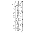
基板10はガラスや石英などの他に、プラスチック材料を用いることができる。また、ステンレスやアルミニウムなどの金属材料の上に絶縁膜を形成したものを用いても良い。この基板10上にゲート電極及びゲート配線(走査線)を形成するための第1導電膜11を形成する。第1導電膜11にはクロム、モリブデン、チタン、タンタル、タングステン、アルミニウムなどの金属材料またはその合金材料を用いる。この第1導電膜11はスパッタリング法や真空蒸着法で形成することができる。(図7(A))
The
第1導電膜11をエッチング加工してゲート電極12、13を形成する。ゲート電極上には第1の半導体膜や配線層を形成するので、その端部がテーパー状になるように加工することが望ましい。また第1導電膜11を、アルミニウムを主成分とする材料で形成する場合には、エッチング加工後に陽極酸化処理などをして表面を絶縁化しておくと良い。また、図示しないがこの工程でゲート電極に接続する配線も同時に形成することができる。(図7(B))
The first
第1絶縁膜14と第2絶縁膜15は、ゲート電極12、13の上層に形成することでゲート絶縁膜として機能させることができる。この場合、第1絶縁膜14として酸化珪素膜、第2絶縁膜15として窒化珪素膜を形成することが好ましい。これらの絶縁膜はグロー放電分解法やスパッタリング法で形成することができる。特に、低い成膜温度でゲートリーク電流が少ない緻密な絶縁膜を形成するには、アルゴンなどの希ガス元素を反応ガスに含ませ、形成される絶縁膜中に混入させると良い。
The first insulating
そして、このような第1、第2絶縁膜上に、第1の半導体膜16を形成する。第1の半導体膜16は、非晶質と結晶構造(単結晶、多結晶を含む)の中間的な構造の半導体を含む膜で形成する。この半導体は、自由エネルギー的に安定な第3の状態を有する半導体であって、短距離秩序を持ち格子歪みを有する結晶質なものであり、その粒径を0.5〜20nmとして非単結晶半導体中に分散させて存在せしめることが可能である。また、未結合手(ダングリングボンド)の中和剤として水素またはハロゲンを少なくとも1原子%またはそれ以上含ませている。ここでは便宜上、このような半導体をセミアモルファス半導体(SAS)と呼ぶ。さらに、ヘリウム、アルゴン、クリプトン、ネオンなどの希ガス元素を含ませて格子歪みをさらに助長させることで安定性が増し良好なSASが得られる。このようなSAS半導体に関する記述は、例えば、米国特許4,409,134号で開示されている。(図7(C))
Then, the
このSASは珪化物気体をグロー放電分解することにより得ることができる。代表的な珪化物気体としては、SiH4であり、その他にもSi2H6、SiH2Cl2、SiHCl3、SiCl4、SiF4などを用いることができる。この珪化物気体を水素、水素とヘリウム、アルゴン、クリプトン、ネオンから選ばれた一種または複数種の希ガス元素で希釈して用いることでSASの形成を容易なものとすることができる。希釈率は10倍〜1000倍の範囲で珪化物気体を希釈することが好ましい。勿論、グロー放電分解による被膜の反応生成は減圧下で行うが、圧力は概略0.1Pa〜133Paの範囲で行えば良い。グロー放電を形成するための電力は1MHz〜120MHz、好ましくは13MHz〜60MHzの高周波電力を供給すれば良い。基板加熱温度は300度以下が好ましく、100〜200度の基板加熱温度が推奨される。 This SAS can be obtained by glow discharge decomposition of a silicide gas. A typical silicide gas is SiH 4 , and in addition, Si 2 H 6 , SiH 2 Cl 2 , SiHCl 3 , SiCl 4 , SiF 4 and the like can be used. The formation of the SAS can be facilitated by diluting the silicide gas with one or plural kinds of rare gas elements selected from hydrogen, hydrogen and helium, argon, krypton, and neon. It is preferable to dilute the silicide gas at a dilution ratio in the range of 10 times to 1000 times. Of course, the reaction of the coating by glow discharge decomposition is performed under reduced pressure, but the pressure may be in the range of about 0.1 Pa to 133 Pa. The power for forming the glow discharge may be high frequency power of 1 MHz to 120 MHz, preferably 13 MHz to 60 MHz. The substrate heating temperature is preferably 300 ° C. or less, and a substrate heating temperature of 100 to 200 ° C. is recommended.
また、珪化物気体中に、CH4、C2H6などの炭化物気体、GeH4、GeF4などのゲルマニウム化気体を混入させて、エネルギーバンド幅を1.5〜2.4eV、若しくは0.9〜1.1eVに調節しても良い。 Further, a carbide gas such as CH 4 and C 2 H 6 and a germanium gas such as GeH 4 and GeF 4 are mixed in the silicide gas, and the energy band width is 1.5 to 2.4 eV, or 0.8. You may adjust to 9-1.1 eV.
また、SASは、価電子制御を目的とした不純物元素を意図的に添加しないときに弱いn型の電気伝導性を示すので、TFTのチャネル形成領域を設ける第1の半導体膜に対しては、p型を付与する不純物元素を、この成膜と同時に、或いは成膜後に添加することで、しきい値制御をすることが可能となる。p型を付与する不純物元素としては、代表的には硼素であり、B2H6、BF3などの不純物気体を1ppm〜1000ppmの割合で珪化物気体に混入させると良い。そしてボロンの濃度を、例えば1×10¹⁴〜6×10¹⁶atoms/cm3とすると良い。 In addition, since SAS exhibits weak n-type conductivity when an impurity element for the purpose of valence electron control is not intentionally added, the first semiconductor film provided with a TFT channel formation region is The threshold value can be controlled by adding an impurity element imparting p-type simultaneously with or after the film formation. The impurity element imparting p-type is typically boron, and an impurity gas such as B 2 H 6 or BF 3 may be mixed into the silicide gas at a rate of 1 ppm to 1000 ppm. The boron concentration is preferably 1 × 10 14 to 6 × 10 16 atoms / cm 3 , for example.
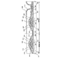
次に、図8(A)に示すように第2の半導体膜17を形成する。第2の半導体膜17は、価電子制御を目的とした不純物元素を意図的に添加しないで形成したものであり、第1の半導体膜16と同様にSASで形成することが好ましい。この第2の半導体膜17は、ソース及びドレインを形成する一導電型を有する第3の半導体膜18と第1の半導体膜16との間に形成することで、バッファ層(緩衝層)的な働きを持っている。従って、弱n型の電気伝導性を持って第1の半導体膜16に対して、同じ導電型で一導電型を有する第3の半導体膜18を形成する場合には必ずしも必要ない。しきい値制御をする目的において、p型を付与する不純物元素を添加する場合には、第2の半導体膜17は段階的に不純物濃度を変化させる効果を持ち、接合形成を良好にする上で好ましい形態となる。すなわち、形成されるTFTにおいては、チャネル形成領域とソースまたはドレイン領域の間に形成される低濃度不純物領域(LDD領域)としての機能を持たせることが可能となる。
Next, as shown in FIG. 8A, a
一導電型を有する第3の半導体膜18はnチャネル型のTFTを形成する場合には、代表的な不純物元素としてリンを添加すれば良く、珪化物気体にPH3などの不純物気体を加えれば良い。一導電型を有する第3の半導体膜18は、SASのような半導体、非晶質半導体、または微結晶半導体で形成することができる。
The
以上、第1絶縁膜14から一導電型を有する第3の半導体膜18までは大気に触れさせることなく連続して形成することが可能である。すなわち、大気成分や大気中に浮遊する汚染不純物元素に汚染されることなく各積層界面を形成することができるので、TFT特性のばらつきを低減することができる。
As described above, the first insulating
次に、フォトレジストを用いてマスク19を形成し、第1の半導体膜16、第2の半導体膜17、一導電型を有する第3の半導体膜18をエッチングして島状に分離形成する。(図8(B))
Next, a
その後、ソース及びドレインに接続する配線を形成するための第2導電膜20を形成する。第2導電膜20はアルミニウム、またはアルミニウムを主成分とする導電性材料で形成するが、半導体膜と接する側の層をチタン、タンタル、モリブデン、タングステン、銅またはこれらの元素の窒化物で形成した積層構造としても良い。例えば1層目がTaで2層目がW、1層目がTaNで2層目がAl、1層目がTaNで2層目がCu、1層目がTiで2層目がAlで3層目がTiといった組み合わせも考えられる。また1層目と2層目のいずれか一方にAgPdCu合金を用いても良い。W、AlとSiの合金(Al−Si)、TiNを順次積層した3層構造としてもよい。Wの代わりに窒化タングステンを用いてもよいし、AlとSiの合金(Al−Si)に代えてAlとTiの合金膜(Al−Ti)を用いてもよいし、TiNに代えてTiを用いてもよい。アルミニウムには耐熱性を向上させるためにチタン、シリコン、スカンジウム、ネオジウム、銅などの元素を0.5〜5原子%添加させても良い。(図8(C))
Thereafter, a second
次にマスク21を形成する。マスク21はソースおよびドレインと接続する配線を形成するためにパターン形成されたマスクであり、同時に第2の半導体膜17及び一導電型を有する第3の半導体膜18を取り除きチャネル形成領域、ソース、ドレイン領域及びLDD領域を形成するためのエッチングマスクとして併用されるものである。アルミニウムまたはこれを主成分とする導電膜のエチングはBCl3、Cl2などの塩化物気体を用いて行えば良い。このエッチング加工で配線23〜26を形成する。また、チャネル形成領域を形成するためのエッチングにはSF6、NF3、CF4などのフッ化物気体を用いてエッチングを行うが、この場合には下地となる第1の半導体膜16とのエッチング選択比をとれないので、処理時間を適宜調整して行うこととなる。以上のようにして、チャネルエッチ型のTFTの構造を形成することができる。(図9(A))
Next, a
次に、チャネル形成領域の保護を目的とした第3絶縁膜27を、窒化珪素膜で形成する。この窒化珪素膜はスパッタリング法やグロー放電分解法で形成可能であるが、大気中に浮遊する有機物や金属物、水蒸気などの汚染不純物の侵入を防ぐためのものであり、緻密な膜であることが要求される。第3絶縁膜27に窒化珪素膜を用いることで、第1の半導体膜16中の酸素濃度を5×10¹⁹atoms/cm3以下、好ましくは1×1019atoms/cm3以下とすることができる。この目的において、珪素をターゲットとして、窒素とアルゴンなどの希ガス元素を混合させたスパッタガスで高周波スパッタリングされた窒化珪素膜で、膜中の希ガス元素を含ませることにより緻密化が促進されることとなる。また、グロー放電分解法においても、珪化物気体をアルゴンなどの不活性ガスで100倍〜500倍に希釈して形成された窒化珪素膜は、100度以下の低温においても緻密な膜を形成可能であり好ましい。さらに必要があれば第4絶縁膜28を酸化珪素膜で積層形成しても良い。第3絶縁膜27と第4絶縁膜28はパッシベーション膜に相当する。
Next, a third insulating
第3絶縁膜27および/または第4絶縁膜28上には、好ましい形態として平坦化膜29を形成する。平坦化膜は、アクリル、ポリイミド、ポリアミドなどの有機樹脂、またはシロキサン系材料を出発材料として形成されたSi−O結合とSi−CHx結合手を含む絶縁膜で形成することが好ましい。これらの材料は含水性があるので、水分の侵入及び放出を防ぐバリア膜として第6絶縁膜30を併設することが好ましい。第6絶縁膜30としては上述のような窒化珪素膜を適用すれば良い。(図9(B))
A
画素電極31は、第6絶縁膜30、平坦化膜29、第3絶縁膜27、第4絶縁膜28にコンタクトホールを形成した後に形成する。(図9(C))
The
以上のようにして形成されたチャネルエッチ型のTFTは、SASでチャネル形成領域を構成することにより2〜10cm2/V・secの電界効果移動度を得ることができる。従って、このTFTを画素のスイッチング用素子として、さらに走査線(ゲート線)側の駆動回路を形成する素子として利用することができる。 The channel-etched TFT formed as described above can obtain a field effect mobility of 2 to 10 cm 2 / V · sec by forming a channel formation region with SAS. Therefore, the TFT can be used as a pixel switching element and an element for forming a driving circuit on the scanning line (gate line) side.
このような、画素のスイッチング素子と走査線側の駆動回路を同じTFTで素子基板は、ゲート電極形成用マスク、半導体領域形成用マスク、配線形成用マスク、コンタクトホール形成用マスク、画素電極形成用マスクの合計5枚のマスクで形成することができる。 The pixel switching element and the scanning line side drive circuit are the same TFT, and the element substrate is a gate electrode forming mask, a semiconductor region forming mask, a wiring forming mask, a contact hole forming mask, and a pixel electrode forming mask. A total of five masks can be formed.
図9(C)では画素のTFTがn型であるので、画素電極31として、陰極を用いるのが望ましいが、逆にp型の場合は陽極を用いるのが望ましい。具体的には、仕事関数が小さい公知の材料、例えば、Ca、Al、CaF、MgAg、AlLi等を用いることができる。
In FIG. 9C, since the TFT of the pixel is n-type, it is preferable to use a cathode as the
次に図10(A)に示すように、第6絶縁膜30上に、有機樹脂膜、無機絶縁膜または有機ポリシロキサンを用いて形成された隔壁33を形成する。隔壁33は開口部を有しており、該開口部において画素電極31が露出している。次に図10(B)に示すように、隔壁33の開口部において画素電極31と接するように、電界発光層34を形成する。電界発光層34は、単数の層で構成されていても、複数の層が積層されるように構成されていてもどちらでも良い。複数の層で構成されている場合、陰極を用いた画素電極31上に、電子注入層、電子輸送層、発光層、ホール輸送層、ホール注入層の順に積層する。
Next, as illustrated in FIG. 10A, a
そして電界発光層34を覆うように、陽極を用いた対向電極35を形成する。対向電極35は、ITO、IZO、ITSOの他、酸化インジウムに2〜20%の酸化亜鉛(ZnO)を混合した透明導電膜を用いることができる。対向電極35として上記透明導電膜の他に、窒化チタン膜またはチタン膜を用いても良い。図10(B)では、対向電極35としITOを用いている。対向電極35は、その表面が平坦化されるように、CMP法、ポリビニルアルコール系の多孔質体で拭浄し、研磨しても良い。またCMP法を用いた研磨後に、対向電極35の表面に紫外線照射、酸素プラズマ処理などを行ってもよい。隔壁33の開口部において、画素電極31と電界発光層34と対向電極35が重なり合うことで、発光素子36が形成されている。
Then, a
なお実際には、図10(B)まで完成したら、さらに外気に曝されないように気密性が高く、脱ガスの少ない保護フィルム(ラミネートフィルム、紫外線硬化樹脂フィルム等)やカバー材でパッケージング(封入)することが好ましい。 Actually, when completed to FIG. 10 (B), it is packaged (covered) with a protective film (laminate film, UV curable resin film, etc.) or cover material that is highly airtight and less degassed so that it is not exposed to the outside air. ) Is preferable.
なお、図7〜図10は、図1に示した構成を有するTFTの作製方法について示したが、図3に示した構成を有するTFTも同様に作製することができる。ただし、図3に示したTFTの場合は、ゲート電極310、320に重畳させて、SASで形成された第1の半導体膜312、322上にチャネル保護膜330、331を形成する点で、図7〜図10と異なっている。
7 to 10 show the manufacturing method of the TFT having the structure shown in FIG. 1, the TFT having the structure shown in FIG. 3 can be similarly manufactured. However, in the case of the TFT shown in FIG. 3, channel
また、図1と図3では、第3絶縁膜(第1のパッシベーション膜)、第4絶縁膜(第2のパッシベーション膜)にコンタクトホールを形成した後、画素電極を形成し、隔壁を形成したものである。隔壁は、アクリル、ポリイミド、ポリアミドなどの有機樹脂、またはシロキサン系材料を出発材料として形成されたSi−O結合とSi−CHx結合手を含む絶縁膜で形成すれば良く、特に感光性の材料を用い、画素電極上に開口部を形成し、その開口部の側壁が連続した曲率を持って形成される傾斜面となるように形成することが好ましい。 Further, in FIGS. 1 and 3, after forming contact holes in the third insulating film (first passivation film) and the fourth insulating film (second passivation film), pixel electrodes are formed, and barrier ribs are formed. Is. The partition wall may be formed of an insulating film including Si—O bonds and Si—CHx bonds formed using an organic resin such as acrylic, polyimide, or polyamide, or a siloxane-based material as a starting material. Preferably, an opening is formed on the pixel electrode, and the side wall of the opening is preferably formed as an inclined surface having a continuous curvature.
本発明で用いることができるセミアモルファスTFTは、n型であってもp型であってもどちらでも良い。ただしセミアモルファスTFTはp型よりもn型の方が、移動度が高く、発光装置の画素に用いるのにより適している。本実施例では、駆動用TFTがn型の場合を例に挙げて、画素の断面構造について説明する。 The semi-amorphous TFT that can be used in the present invention may be either n-type or p-type. However, the semi-amorphous TFT has higher mobility in the n-type than in the p-type, and is more suitable for use in the pixel of the light-emitting device. In this embodiment, a cross-sectional structure of a pixel will be described with an example in which a driving TFT is an n-type.
図11(A)に、駆動用TFT7001がn型で、発光素子7002から発せられる光が陽極7005側に抜ける場合の、画素の断面図を示す。図11(A)では、発光素子7002の陰極7003と駆動用TFT7001が電気的に接続されており、陰極7003上に電界発光層7004、陽極7005が順に積層されている。陰極7003は仕事関数が小さく、なおかつ光を反射する導電膜であれば公知の材料を用いることができる。例えば、Ca、Al、CaF、MgAg、AlLi等が望ましい。そして電界発光層7004は、単数の層で構成されていても、複数の層が積層されるように構成されていてもどちらでも良い。複数の層で構成されている場合、陰極7003上に電子注入層、電子輸送層、発光層、ホール輸送層、ホール注入層の順に積層する。なおこれらの層を全て設ける必要はない。陽極7005は光を透過する透明導電膜を用いて形成し、例えばITO、IZO、ITSOの他、酸化インジウムに2〜20%の酸化亜鉛(ZnO)を混合した透明導電膜を用いても良い。 FIG. 11A is a cross-sectional view of a pixel in the case where the driving TFT 7001 is n-type and light emitted from the light-emitting element 7002 passes to the anode 7005 side. In FIG. 11A, a cathode 7003 of a light emitting element 7002 and a driving TFT 7001 are electrically connected, and an electroluminescent layer 7004 and an anode 7005 are sequentially stacked over the cathode 7003. A known material can be used for the cathode 7003 as long as it has a small work function and reflects light. For example, Ca, Al, CaF, MgAg, AlLi, etc. are desirable. The electroluminescent layer 7004 may be composed of a single layer or a plurality of layers stacked. In the case of a plurality of layers, an electron injection layer, an electron transport layer, a light emitting layer, a hole transport layer, and a hole injection layer are stacked in this order on the cathode 7003. It is not necessary to provide all these layers. The anode 7005 is formed using a transparent conductive film that transmits light. For example, in addition to ITO, IZO, and ITSO, a transparent conductive film in which 2 to 20% zinc oxide (ZnO) is mixed with indium oxide may be used.
陰極7003と、電界発光層7004と、陽極7005とが重なっている部分が発光素子7002に相当する。図11(A)に示した画素の場合、発光素子7002から発せられる光は、白抜きの矢印で示すように陽極7005側に抜ける。 A portion where the cathode 7003, the electroluminescent layer 7004, and the anode 7005 overlap corresponds to the light emitting element 7002. In the case of the pixel shown in FIG. 11A, light emitted from the light-emitting element 7002 passes to the anode 7005 side as indicated by a white arrow.
図11(B)に、駆動用TFT7011がn型で、発光素子7012から発せられる光が陰極7013側に抜ける場合の、画素の断面図を示す。図11(B)では、駆動用TFT7011と電気的に接続された透明導電膜7017上に、発光素子7012の陰極7013が成膜されており、陰極7013上に電界発光層7014、陽極7015が順に積層されている。そして陽極7015を覆うように、光を反射または遮蔽するための遮蔽膜7016が成膜されている。陰極7013は、図11(A)の場合と同様に、仕事関数が小さい導電膜であれば公知の材料を用いることができる。ただしその膜厚は、光を透過する程度(好ましくは、5nm〜30nm程度)とする。例えば20nmの膜厚を有するAlを、陰極7013として用いることができる。そして電界発光層7014は、図11(A)と同様に、単数の層で構成されていても、複数の層が積層されるように構成されていてもどちらでも良い。陽極7015は光を透過する必要はないが、図11(A)と同様に、透明導電膜を用いて形成することができる。そして遮蔽膜7016は、例えば光を反射する金属等を用いることができるが、金属膜に限定されない。例えば黒の顔料添加した樹脂等を用いることもできる。 FIG. 11B is a cross-sectional view of a pixel in the case where the driving TFT 7011 is an n-type and light emitted from the light-emitting element 7012 passes to the cathode 7013 side. In FIG. 11B, a cathode 7013 of a light-emitting element 7012 is formed over a transparent conductive film 7017 electrically connected to the driving TFT 7011. An electroluminescent layer 7014 and an anode 7015 are sequentially formed over the cathode 7013. Are stacked. A shielding film 7016 for reflecting or shielding light is formed so as to cover the anode 7015. As in the case of FIG. 11A, a known material can be used for the cathode 7013 as long as it is a conductive film having a low work function. However, the film thickness is set so as to transmit light (preferably, about 5 nm to 30 nm). For example, Al having a thickness of 20 nm can be used as the cathode 7013. In addition, as in FIG. 11A, the electroluminescent layer 7014 may be formed of a single layer or a stack of a plurality of layers. The anode 7015 is not required to transmit light, but can be formed using a transparent conductive film as in FIG. The shielding film 7016 can be formed using, for example, a metal that reflects light, but is not limited to a metal film. For example, a resin to which a black pigment is added can be used.
陰極7013と、電界発光層7014と、陽極7015とが重なっている部分が発光素子7012に相当する。図11(B)に示した画素の場合、発光素子7012から発せられる光は、白抜きの矢印で示すように陰極7013側に抜ける。 A portion where the cathode 7013, the electroluminescent layer 7014, and the anode 7015 overlap corresponds to the light emitting element 7012. In the case of the pixel shown in FIG. 11B, light emitted from the light-emitting element 7012 passes to the cathode 7013 side as shown by a hollow arrow.
次に図11(C)を用いて、駆動用TFT7021がn型で、発光素子7022から発せられる光が陽極7025側と陰極7023側の両方から抜ける場合の、画素の断面図を示す。図11(C)では、駆動用TFT7021と電気的に接続された透明導電膜7027上に、発光素子7022の陰極7023が成膜されており、陰極7023上に電界発光層7024、陽極7025が順に積層されている。陰極7023は、図11(A)の場合と同様に、仕事関数が小さい導電膜であれば公知の材料を用いることができる。ただしその膜厚は、光を透過する程度とする。例えば20nmの膜厚を有するAlを、陰極7023として用いることができる。そして電界発光層7024は、図11(A)と同様に、単数の層で構成されていても、複数の層が積層されるように構成されていてもどちらでも良い。陽極7025は、図11(A)と同様に、光を透過する透明導電膜を用いて形成することができる。 Next, FIG. 11C is a cross-sectional view of a pixel in the case where the driving TFT 7021 is n-type and light emitted from the light-emitting element 7022 is emitted from both the anode 7025 side and the cathode 7023 side. In FIG. 11C, the cathode 7023 of the light-emitting element 7022 is formed over the transparent conductive film 7027 electrically connected to the driving TFT 7021. The electroluminescent layer 7024 and the anode 7025 are sequentially formed over the cathode 7023. Are stacked. As in the case of FIG. 11A, a known material can be used for the cathode 7023 as long as it is a conductive film having a low work function. However, the film thickness is set so as to transmit light. For example, Al having a thickness of 20 nm can be used as the cathode 7023. In addition, as in FIG. 11A, the electroluminescent layer 7024 may be formed of a single layer or a stack of a plurality of layers. The anode 7025 can be formed using a transparent conductive film that transmits light, as in FIG.
陰極7023と、電界発光層7024と、陽極7025とが重なっている部分が発光素子7022に相当する。図11(C)に示した画素の場合、発光素子7022から発せられる光は、白抜きの矢印で示すように陽極7025側と陰極7023側の両方に抜ける。 A portion where the cathode 7023, the electroluminescent layer 7024, and the anode 7025 overlap corresponds to the light-emitting element 7022. In the case of the pixel shown in FIG. 11C, light emitted from the light-emitting element 7022 passes through both the anode 7025 side and the cathode 7023 side as indicated by white arrows.
なお本実施例では、駆動用TFTと発光素子が電気的に接続されている例を示したが、駆動用TFTと発光素子との間に電流制御用TFTが接続されている構成であってもよい。 In this embodiment, an example in which the driving TFT and the light emitting element are electrically connected is shown. However, even in a configuration in which a current control TFT is connected between the driving TFT and the light emitting element. Good.
なお、図11(A)〜図11(C)に示す全ての画素において、発光素子を覆うように保護膜を成膜しても良い。保護膜は水分や酸素などの発光素子の劣化を促進させる原因となる物質を、他の絶縁膜と比較して透過させにくい膜を用いる。代表的には、例えばDLC膜、窒化炭素膜、RFスパッタ法で形成された窒化珪素膜等を用いるのが望ましい。また上述した水分や酸素などの物質を透過させにくい膜と、該膜に比べて水分や酸素などの物質を透過させやすい膜とを積層させて、保護膜として用いることも可能である。 Note that a protective film may be formed so as to cover the light-emitting elements in all the pixels illustrated in FIGS. As the protective film, a film that hardly transmits a substance that causes deterioration of the light-emitting element, such as moisture or oxygen, as compared with other insulating films is used. Typically, it is desirable to use, for example, a DLC film, a carbon nitride film, a silicon nitride film formed by an RF sputtering method, or the like. In addition, the above-described film that hardly transmits a substance such as moisture or oxygen and a film that easily allows a substance such as moisture or oxygen to pass through can be stacked to be used as a protective film.
また、図11(B)、図11(C)において、陰極側から光を得るためには、陰極の膜厚を薄くする方法の他に、Liを添加することで仕事関数が小さくなったITOを用いる方法もある。 In FIGS. 11B and 11C, in order to obtain light from the cathode side, in addition to the method of reducing the thickness of the cathode, ITO whose work function is reduced by adding Li is used. There is also a method using.
なお本発明の発光装置は、図11に示した構成に限定されるものではなく、本発明の技術的思想に基づく各種の変形が可能である。 The light emitting device of the present invention is not limited to the configuration shown in FIG. 11, and various modifications based on the technical idea of the present invention are possible.
本実施例では、本発明の発光装置が有する、セミアモルファスTFTを用いた画素のバリエーションについて説明する。 In this embodiment, a variation of a pixel using a semi-amorphous TFT included in the light-emitting device of the present invention will be described.
図12(A)に、本実施例の画素の一形態を示す。図12(A)に示す画素は、発光素子901と、画素へのビデオ信号の入力を制御するためのスイッチング素子として用いるスイッチング用TFT902と、発光素子901に流れる電流値を制御する駆動用TFT903と、発光素子901への電流の供給の有無を選択するための電流制御用TFT904とを有している。さらに本実施例のように、ビデオ信号の電位を保持するための容量素子905を画素に設けても良い。
FIG. 12A illustrates one mode of a pixel of this example. A pixel illustrated in FIG. 12A includes a light-emitting
スイッチング用TFT902、駆動用TFT903及び電流制御用TFT904はn型であってもp型であってもどちらでも良いが、全て同じ極性を有する。そして駆動用TFT903を飽和領域で、電流制御用TFT904を線形領域で動作させる。
The switching
また、駆動用TFT903のLをWより長く、電流制御用TFT904のLをWと同じか、それより短くてもよい。より望ましくは、駆動用TFT903のWに対するLの比が5以上にするとよい。上記構成によって、駆動用TFT903の特性の違いに起因する、画素間における発光素子901の輝度のばらつきをさらに抑えることができる。また、駆動用TFTのチャネル長をL1、チャネル幅をW1、電流制御用TFTのチャネル長をL2、チャネル幅をW2とすると、L1/W1:L2/W2=X:1のとき、Xは5以上6000以下とするのが望ましい。例えばX=6000の場合、L1/W1=500μm/3μm、L2/W2=3μm/100μmとするのが望ましい。
Further, L of the driving
スイッチング用TFT902のゲート電極は、走査線Gに接続されている。スイッチング用TFT902のソースとドレインは、一方が信号線Sに、もう一方が電流制御用TFT904のゲート電極に接続されている。駆動用TFT903のゲート電極は第2の電源線Vbに接続されている。そして駆動用TFT903及び電流制御用TFT904は、第1の電源線Vaから供給される電流が、駆動用TFT903及び電流制御用TFT904のドレイン電流として発光素子901に供給されるように、第1の電源線Va、発光素子901と接続されている。本実施例では、電流制御用TFT904のソースが第1の電源線Vaに接続され、駆動用TFT903のドレインが発光素子901の画素電極に接続される。
The gate electrode of the switching
なお駆動用TFT903のソースを第1の電源線Vaに接続し、電流制御用TFT904のドレインを発光素子901の画素電極に接続してもよい。
Note that the source of the driving
発光素子901は陽極と陰極と、陽極と陰極との間に設けられた電界発光層とからなる。図12(A)のように、陰極が駆動用TFT903と接続している場合、陰極が画素電極、陽極が対向電極となる。発光素子901の対向電極と、第1の電源線Vaのそれぞれには、発光素子901に順バイアス方向の電流が供給されるように、電位差が設けられている。発光素子901の対向電極は、補助電極Wと接続されている。
The light-emitting
容量素子905が有する2つの電極は、一方は第1の電源線Vaに接続されており、もう一方は電流制御用TFT904のゲート電極に接続されている。容量素子905はスイッチング用TFT902が非選択状態(オフ状態)にある時、容量素子905の電極間の電位差を保持するために設けられている。なお図12(A)では容量素子905を設ける構成を示したが、図12(A)に示す画素はこの構成に限定されず、容量素子905を設けない構成にしても良い。
One of the two electrodes of the
図12(A)では駆動用TFT903および電流制御用TFT904をn型とし、駆動用TFT903のドレインと発光素子901の陰極とを接続した。逆に駆動用TFT903および電流制御用TFT904をp型とするならば、駆動用TFT903のソースと発光素子901の陽極とを接続する。この場合、発光素子901の陽極が画素電極、陰極が対向電極となる。
In FIG. 12A, the driving
次に、図12(B)に、図12(A)に示した画素に、電流制御用TFT904を強制的にオフするためのTFT(消去用TFT)906を設けた画素の回路図を示す。なお図12(B)では、図12(A)において既に説明した素子については、同じ符号を付して示す。なお第1の走査線は第2の走査線と区別するために、Gaで示し、第2の走査線をGbとして示す。消去用TFT906は、ゲート電極が第2の走査線Gbに接続されており、ソースとドレインは、一方が電流制御用TFT904のゲート電極に、他方が第1の電源線Vaに接続されている。消去用TFT906はn型であってもp型であってもどちらでも良いが、画素内の他のTFTと同じ極性を有する。
Next, FIG. 12B is a circuit diagram of a pixel in which a TFT (erasing TFT) 906 for forcibly turning off the
次に、図12(C)に、図12(A)に示した画素において、駆動用TFT903のゲート電極を、第2の走査線Gbに接続する画素の回路図を示す。なお図12(C)では、図12(A)において既に説明した素子については、同じ符号を付して示す。図12(C)に示すように、駆動用TFT903のゲート電極に与える電位を切り替えることで、ビデオ信号が有する情報に関わらず、発光素子901の発光を強制的に終了させることができる。
Next, FIG. 12C is a circuit diagram of a pixel in which the gate electrode of the driving
次に、図12(D)に、図12(C)に示した画素において、電流制御用TFT904を強制的にオフするためのTFT(消去用TFT)906を設けた画素の回路図を示す。なお図12(D)では、図12(A)〜図12(D)及び図12(C)において既に説明した素子については、同じ符号を付して示す。消去用TFT906は、ゲート電極が第2の走査線Gbに接続されており、ソースとドレインは、一方が電流制御用TFT904のゲート電極に、他方が電源線Vに接続されている。消去用TFT906はn型であってもp型であってもどちらでも良いが、画素内の他のTFTと同じ極性を有する。
Next, FIG. 12D is a circuit diagram of a pixel provided with a TFT (erase TFT) 906 for forcibly turning off the
次に、図12(E)に、電流制御用TFTを設けない画素の構成を示す。図12(E)において、911は発光素子、912はスイッチング用TFT、913は駆動用TFT、915は容量素子、916は消去用TFT916に相当する。スイッチング用TFT912は、ゲート電極が第1の走査線Gaに接続されており、ソースとドレインが、一方は信号線Sに、他方が駆動用TFT913のゲート電極に接続されている。駆動用TFT913は、ソースが電源線Vに、ドレインが発光素子911の画素電極に接続されている。発光素子911の対向電極は補助電極Wに接続されている。消去用TFT916は、ゲート電極が第2の走査線Gbに、ソースとドレインは、一方が駆動用TFT913のゲート電極に、他方が電源線Vに接続されている。
Next, FIG. 12E illustrates a structure of a pixel in which a current control TFT is not provided. In FIG. 12E, 911 corresponds to a light emitting element, 912 corresponds to a switching TFT, 913 corresponds to a driving TFT, 915 corresponds to a capacitor element, and 916 corresponds to an erasing
なお、本発明の発光装置が有する画素の構成は、本実施例で示した構成に限定されない。 Note that the structure of the pixel included in the light-emitting device of the present invention is not limited to the structure shown in this embodiment.
本実施例では、本発明の発光装置が有するセミアモルファスTFTの、一形態について説明する。 In this example, one mode of a semi-amorphous TFT included in the light-emitting device of the present invention will be described.
図13(A)に、本実施例のセミアモルファスTFTの上面図を、図13(B)に、図13(A)のA−A’における断面図を示す。1301は、その一部がゲート電極として機能するゲート配線であり、ゲート絶縁膜を1302間に挟んで、セミアモルファス半導体で形成された第1の半導体膜1303と重なっている。また、第1の半導体膜1303と接するように、LDD領域として機能する第2の半導体膜1304a、1304bが形成されており、第2の半導体膜1304a、1304bに接するように、一導電型を有する第3の半導体膜1305a、1305bが形成されている。また1306、1307は、第3の半導体膜1305a、1305bとそれぞれ接する配線に相当する。
FIG. 13A is a top view of the semi-amorphous TFT of this example, and FIG. 13B is a cross-sectional view taken along line A-A ′ of FIG. A
図13に示すセミアモルファスTFTにおいて、第3の半導体膜1305aと第3の半導体膜1305bの間隔を一定にすることで、チャネル長を一定に保つことができる。また、第3の半導体膜1305bの端部を第3の半導体膜1305aで囲むようにレイアウトすることで、チャネル形成領域のドレイン領域側において、電界が集中するのを緩和することができる。さらに、チャネル長に対するチャネル幅の比を高くすることができるので、オン電流を高めることができる。
In the semi-amorphous TFT shown in FIG. 13, the channel length can be kept constant by keeping the distance between the
本実施例では、極性が全て同一のセミアモルファスTFTを用いた、シフトレジスタの一形態について説明する。図14(A)に、本実施例のシフトレジスタの構成を示す。図14(A)に示すシフトレジスタは、第1のクロック信号CLK、第2のクロック信号CLKb、スタートパルス信号SPを用いて動作する。1401はパルス出力回路であり、その具体的な構成を、図14(B)に示す。 In this embodiment, an example of a shift register using semi-amorphous TFTs having the same polarity will be described. FIG. 14A shows the structure of the shift register of this embodiment. The shift register illustrated in FIG. 14A operates using the first clock signal CLK, the second clock signal CLKb, and the start pulse signal SP. Reference numeral 1401 denotes a pulse output circuit, and its specific structure is shown in FIG.
パルス出力回路1401は、TFT801〜806と、容量素子807を有する。TFT801は、ゲートがノード2に、ソースがTFT805のゲートに接続されており、ドレインに電位Vddが与えられている。TFT802は、ゲートがTFT806のゲートに、ドレインがTFT805のゲートに接続されており、ソースに電位Vssが与えられている。TFT803は、ゲートがノード3に、ソースがTFT806のゲートに接続されており、ドレインに電位Vddが与えられている。TFT804は、ゲートがノード2に、ドレインがTFT805のゲートに接続されており、ソースに電位Vssが与えられている。TFT805は、ゲートが容量素子807の一方の電極に、ドレインがノード1に、ソースが容量素子807の他方の電極及びノード4に接続されている。またTFT806は、ゲートが容量素子807の一方の電極に、ドレインがノード4に接続されており、ソースに電位Vssが与えられている。
The pulse output circuit 1401 includes TFTs 801 to 806 and a capacitor 807. The TFT 801 has a gate connected to the node 2, a source connected to the gate of the TFT 805, and a potential Vdd applied to the drain. The TFT 802 has a gate connected to the gate of the TFT 806, a drain connected to the gate of the TFT 805, and a potential Vss applied to the source. The TFT 803 has a gate connected to the node 3, a source connected to the gate of the TFT 806, and a potential Vdd applied to the drain. The TFT 804 has a gate connected to the node 2, a drain connected to the gate of the TFT 805, and a potential Vss applied to the source. The TFT 805 has a gate connected to one electrode of the capacitor 807, a drain connected to the
次に、図14(B)に示すパルス出力回路1401の動作について説明する。ただし、CLK、CLKb、SPは、HレベルのときVdd、LレベルのときVssとし、さらに説明を簡単にするためVss=0と仮定する。 Next, operation of the pulse output circuit 1401 illustrated in FIG. 14B is described. However, it is assumed that CLK, CLKb, and SP are Vdd when the signal is at the H level and Vss when the signal is at the L level, and Vss = 0 for simplifying the description.
SPがHレベルになると、TFT801がオンになるため、TFT805のゲートの電位が上昇していく。そして最終的には、TFT805のゲートの電位がVdd−Vth(VthはTFT801〜806のしきい値とする)となったところで、TFT801がオフし、浮遊状態となる。一方、SPがHレベルになるとTFT804がオンになるため、TFT802、806のゲートの電位は下降し、最終的にはVssとなり、TFT802、806はオフになる。TFT803のゲートは、このときLレベルとなっており、オフしている。 When SP becomes H level, the TFT 801 is turned on, so that the gate potential of the TFT 805 rises. Finally, when the gate potential of the TFT 805 becomes Vdd-Vth (Vth is a threshold value of the TFTs 801 to 806), the TFT 801 is turned off and enters a floating state. On the other hand, when SP becomes H level, the TFT 804 is turned on, so that the gate potentials of the TFTs 802 and 806 are lowered to finally Vss, and the TFTs 802 and 806 are turned off. At this time, the gate of the TFT 803 is at the L level and is turned off.
次にSPはLレベルとなり、TFT801、804がオフし、TFT805のゲートの電位がVdd−Vthで保持される。ここで、TFT805のゲート/ソース間電圧がそのしきい値Vthを上回っていれば、TFT805がオンする。 Next, SP becomes L level, the TFTs 801 and 804 are turned off, and the gate potential of the TFT 805 is held at Vdd−Vth. Here, if the gate-source voltage of the TFT 805 exceeds the threshold value Vth, the TFT 805 is turned on.
次に、ノード1に与えられているCLKがLレベルからHレベルに変わると、TFT805がオンしているので、ノード4、すなわちTFT805のソースの電位が上昇を始める。そしてTFT805のゲート/ソース間には容量素子807による容量結合が存在しているため、ノード4の電位上昇に伴い、浮遊状態となっているTFT805のゲートの電位が再び上昇する。最終的には、TFT805のゲートの電位は、Vdd+Vthよりも高くなり、ノード4の電位はVddに等しくなる。そして、上述の動作を2段目以降のパルス出力回路1401において同様行なわれ、順にパルスが出力される。
Next, when the CLK applied to the
本実施例では、本発明の発光装置の一形態に相当するパネルの外観について、図15を用いて説明する。図15は、第1の基板上に形成されたセミアモルファスTFT及び発光素子を、第2の基板との間にシール材によって封止した、パネルの上面図であり、図15(B)は、図15(A)のA−A’における断面図に相当する。 In this example, the appearance of a panel corresponding to one embodiment of the light-emitting device of the present invention will be described with reference to FIG. FIG. 15 is a top view of a panel in which a semi-amorphous TFT and a light-emitting element formed over a first substrate are sealed with a sealant between the second substrate and FIG. This corresponds to a cross-sectional view taken along line AA ′ in FIG.
第1の基板4001上に設けられた画素部4002と、走査線駆動回路4004とを囲むようにして、シール材4005が設けられている。また画素部4002と、走査線駆動回路4004の上に第2の基板4006が設けられている。よって画素部4002と、走査線駆動回路4004とは、第1の基板4001とシール材4005と第2の基板4006とによって、充填材4007と共に密封されている。また第1の基板4001上のシール材4005によって囲まれている領域とは異なる領域に、別途用意された基板上に多結晶半導体膜で形成された信号線駆動回路4003が実装されている。なお本実施例では、多結晶半導体膜を用いたTFTを有する信号線駆動回路を、第1の基板4001に貼り合わせる例について説明するが、単結晶半導体を用いたトランジスタで信号線駆動回路を形成し、貼り合わせるようにしても良い。図15では、信号線駆動回路4003に含まれる、多結晶半導体膜で形成されたTFT4009を例示する。
A sealant 4005 is provided so as to surround the pixel portion 4002 provided over the
また第1の基板4001上に設けられた画素部4002と、走査線駆動回路4004は、TFTを複数有しており、図15(B)では、画素部4002に含まれるTFT4010とを例示している。なお本実施例では、TFT4010が駆動用TFTであると仮定するが、TFT4010は電流制御用TFTであっても良いし、消去用TFTであっても良い。TFT4010はセミアモルファス半導体を用いたTFTに相当する。
In addition, the pixel portion 4002 provided over the
また4011は発光素子に相当し、発光素子4011が有する画素電極は、TFT4010のドレインと、配線4017を介して電気的に接続されている。そして本実施例では、発光素子4011の対向電極と透明導電膜4012が電気的に接続されている。なお発光素子4011の構成は、本実施の形態に示した構成に限定されない。発光素子4011から取り出す光の方向や、TFT4010の極性などに合わせて、発光素子4011の構成は適宜変えることができる。
また、別途形成された信号線駆動回路4003と、走査線駆動回路4004または画素部4002に与えられる各種信号及び電位は、図15(B)に示す断面図では図示されていないが、引き回し配線4014及び4015を介して、接続端子4016から供給されている。
In addition, a variety of signals and potentials are supplied to the signal line driver circuit 4003 and the scan line driver circuit 4004 or the pixel portion 4002 which are separately formed, which are not illustrated in the cross-sectional view in FIG. And 4015 through a
本実施例では、接続端子4016が、発光素子4011が有する画素電極と同じ導電膜から形成されている。また、引き回し配線4014は、配線4017と同じ導電膜から形成されている。また引き回し配線4015は、TFT4010が有するゲート電極と、同じ導電膜から形成されている。
In this embodiment, the
接続端子4016は、FPC4018が有する端子と、異方性導電膜4019を介して電気的に接続されている。
The
なお、第1の基板4001、第2の基板4006としては、ガラス、金属(代表的にはステンレス)、セラミックス、プラスチックを用いることができる。プラスチックとしては、FRP(Fiberglass−Reinforced Plastics)板、PVF(ポリビニルフルオライド)フィルム、マイラーフィルム、ポリエステルフィルムまたはアクリル樹脂フィルムを用いることができる。また、アルミニウムホイルをPVFフィルムやマイラーフィルムで挟んだ構造のシートを用いることもできる。
Note that as the
但し、発光素子4011からの光の取り出し方向に位置する基板には、第2の基板は透明でなければならない。その場合には、ガラス板、プラスチック板、ポリエステルフィルムまたはアクリルフィルムのような透光性を有する材料を用いる。
However, the second substrate must be transparent to the substrate positioned in the light extraction direction from the
また、充填材4007としては窒素やアルゴンなどの不活性な気体の他に、紫外線硬化樹脂または熱硬化樹脂を用いることができ、PVC(ポリビニルクロライド)、アクリル、ポリイミド、エポキシ樹脂、シリコン樹脂、PVB(ポリビニルブチラル)またはEVA(エチレンビニルアセテート)を用いることができる。本実施例では充填材として窒素を用いた。 As the filler 4007, in addition to an inert gas such as nitrogen or argon, an ultraviolet curable resin or a thermosetting resin can be used. PVC (polyvinyl chloride), acrylic, polyimide, epoxy resin, silicon resin, PVB (Polyvinyl butyral) or EVA (ethylene vinyl acetate) can be used. In this example, nitrogen was used as the filler.
なお図15では、信号線駆動回路4003を別途形成し、第1の基板4001に実装している例を示しているが、本実施例はこの構成に限定されない。走査線駆動回路を別途形成して実装しても良いし、信号線駆動回路の一部または走査線駆動回路の一部のみを別途形成して実装しても良い。
Note that FIG. 15 illustrates an example in which the signal line driver circuit 4003 is separately formed and mounted on the
本実施例は、他の実施例に記載した構成と組み合わせて実施することが可能である。 This embodiment can be implemented in combination with the structure described in other embodiments.
発光素子を用いた発光装置は自発光型であるため、液晶ディスプレイに比べ、明るい場所での視認性に優れ、視野角が広い。従って、様々な電子機器の表示部に用いることができる。 Since a light-emitting device using a light-emitting element is a self-luminous type, it has excellent visibility in a bright place and a wide viewing angle compared to a liquid crystal display. Therefore, it can be used for display portions of various electronic devices.
本発明の発光装置を用いた電子機器として、ビデオカメラ、デジタルカメラ、ゴーグル型ディスプレイ(ヘッドマウントディスプレイ)、ナビゲーションシステム、音響再生装置(カーオーディオ、オーディオコンポ等)、ノート型パーソナルコンピュータ、ゲーム機器、携帯情報端末(モバイルコンピュータ、携帯電話、携帯型ゲーム機または電子書籍等)、記録媒体を備えた画像再生装置(具体的にはDVD:Digital Versatile Disc)等の記録媒体を再生し、その画像を表示しうるディスプレイを備えた装置)などが挙げられる。特に携帯用電子機器の場合、斜め方向から画面を見る機会が多く、視野角の広さが重要視されるため、発光装置を用いることが望ましい。また本発明では、半導体膜の成膜後に結晶化の工程を設ける必要がないので、比較的パネルの大型化が容易であるため、10〜50インチの大型のパネルを用いた電子機器に非常に有用である。それら電子機器の具体例を図16に示す。 As an electronic device using the light emitting device of the present invention, a video camera, a digital camera, a goggle type display (head mounted display), a navigation system, a sound reproduction device (car audio, audio component, etc.), a notebook personal computer, a game device, Play back a recording medium such as a portable information terminal (mobile computer, mobile phone, portable game machine or electronic book), an image playback device (specifically a DVD: Digital Versatile Disc) equipped with a recording medium, and display the image. A device having a display capable of displaying). In particular, in the case of a portable electronic device, it is desirable to use a light-emitting device because there are many opportunities to see the screen from an oblique direction and the wide viewing angle is important. In the present invention, since it is not necessary to provide a crystallization step after the formation of the semiconductor film, it is relatively easy to increase the size of the panel. Therefore, the present invention is very suitable for an electronic device using a large panel of 10-50 inches. Useful. Specific examples of these electronic devices are shown in FIGS.
図16(A)は表示装置であり、筐体2001、支持台2002、表示部2003、スピーカー部2004、ビデオ入力端子2005等を含む。本発明の発光装置を表示部2003に用いることで、本発明の表示装置が完成する。発光装置は自発光型であるためバックライトが必要なく、液晶ディスプレイよりも薄い表示部とすることができる。なお、発光素子表示装置は、パーソナルコンピュータ用、TV放送受信用、広告表示用などの全ての情報表示用表示装置が含まれる。
FIG. 16A illustrates a display device, which includes a
図16(B)はノート型パーソナルコンピュータであり、本体2201、筐体2202、表示部2203、キーボード2204、外部接続ポート2205、ポインティングマウス2206等を含む。本発明の発光装置を表示部2203に用いることで、本発明のノート型パーソナルコンピュータが完成する。
FIG. 16B illustrates a laptop personal computer, which includes a
図16(C)は記録媒体を備えた携帯型の画像再生装置(具体的にはDVD再生装置)であり、本体2401、筐体2402、表示部A2403、表示部B2404、記録媒体(DVD等)読み込み部2405、操作キー2406、スピーカー部2407等を含む。表示部A2403は主として画像情報を表示し、表示部B2404は主として文字情報を表示する。なお、記録媒体を備えた画像再生装置には家庭用ゲーム機器なども含まれる。本発明の発光装置を表示部A2403、B2404に用いることで、本発明の画像再生装置が完成する。
FIG. 16C illustrates a portable image reproducing device (specifically, a DVD reproducing device) provided with a recording medium, which includes a
また、発光装置は発光している部分が電力を消費するため、発光部分が極力少なくなるように情報を表示することが望ましい。従って、携帯情報端末、特に携帯電話や音響再生装置のような文字情報を主とする表示部に発光装置を用いる場合には、非発光部分を背景として文字情報を発光部分で形成するように駆動することが望ましい。 In addition, since the light emitting device consumes power in the light emitting portion, it is desirable to display information so that the light emitting portion is minimized. Therefore, when a light emitting device is used for a display unit mainly including character information, such as a portable information terminal, particularly a mobile phone or a sound reproduction device, it is driven so that character information is formed by the light emitting part with the non-light emitting part as the background. It is desirable to do.
以上の様に、本発明の適用範囲は極めて広く、あらゆる分野の電子機器に用いることが可能である。また、本実施例の電子機器は、実施例1〜4に示したいずれの構成の発光装置を用いても良い。
As described above, the applicable range of the present invention is so wide that it can be used for electronic devices in various fields. In addition, the electronic device of this embodiment may use the light emitting device having any structure shown in
100 基板
101 TFT
102 TFT
103 発光素子
110 ゲート電極
111 ゲート絶縁膜
112 第1の半導体膜
113 第2の半導体膜
114 第3の半導体膜
115 配線
120 ゲート電極
122 第1の半導体膜
123 第2の半導体膜
124 第3の半導体膜
125 配線
130 画素電極
131 電界発光層
132 対向電極
140 パッシベーション膜
141 パッシベーション膜
201 スイッチング用TFT
202 駆動用TFT
203 発光素子
204 容量素子
205 画素電極
300 基板
301 TFT
302 TFT
303 発光素子
310 ゲート電極
311 ゲート絶縁膜
312 第1の半導体膜
313 第2の半導体膜
314 第3の半導体膜
315 配線
325 配線
332 対向電極
340 パッシベーション膜
341 パッシベーション膜
330 チャネル保護膜
370 画素電極
371 電界発光層
701 画素部
702 走査線駆動回路
703 信号線駆動回路
704 シフトレジスタ
705 アナログスイッチ
706 シフトレジスタ
707 バッファ
712 走査線駆動回路
713 信号線駆動回路
714 シフトレジスタ
715 ラッチA
716 ラッチB
801 TFT
802 TFT
803 TFT
804 TFT
805 TFT
806 TFT
807 容量素子
901 発光素子
902 スイッチング用TFT
903 駆動用TFT
904 電流制御用TFT
905 容量素子
906 消去用TFT
911 発光素子
912 スイッチング用TFT
913 駆動用TFT
916 消去用TFT
100
102 TFT
103
202 Driving TFT
203
302 TFT
303 Light-Emitting
716 Latch B
801 TFT
802 TFT
803 TFT
804 TFT
805 TFT
806 TFT
807
903 Driving TFT
904 Current control TFT
905
911 Light-emitting
913 Driving TFT
916 TFT for erasing
Claims (6)
複数のゲート電極上にゲート絶縁膜を形成し、
前記ゲート絶縁膜上に、セミアモルファス構造を有する第1の半導体膜を、珪化物気体をグロー放電分解し、且つしきい値制御のための第1の不純物元素を前記第1の半導体膜がI型に近づくように添加しながら形成し、
前記第1の半導体膜上に、第2の半導体膜を前記第1の不純物元素を添加せずに形成し、
前記第2の半導体膜上に、前記第2の半導体膜よりも導電性が高く、一導電型を付与する不純物が添加された第3の半導体膜を、一導電型を付与する第2の不純物元素を添加しながら形成し、
前記第1乃至第3の半導体膜をエッチングして、複数の島状半導体膜を形成し、
前記複数のゲート電極、前記ゲート絶縁膜、及び前記複数の島状半導体膜を用いて、前記複数の逆スタガ型TFTを形成し、
前記第1乃至第3の半導体膜は、大気に触れさせることなく連続的に成膜することにより形成し、
前記第1の不純物元素は、前記第2の不純物元素と逆の導電性を付与する不純物元素であることを特徴とするシステムオンパネル型の発光装置の作製方法。 A method for manufacturing a system-on-panel type light emitting device provided with a plurality of inverted staggered TFTs,
Forming a gate insulating film on the plurality of gate electrodes;
A first semiconductor film having a semi-amorphous structure is formed on the gate insulating film by glow discharge decomposition of a silicide gas, and a first impurity element for controlling a threshold value is defined as I Form while adding so as to approach the mold ,
Forming a second semiconductor film on the first semiconductor film without adding the first impurity element ;
A third semiconductor film having conductivity higher than that of the second semiconductor film and added with an impurity imparting one conductivity type over the second semiconductor film is used as a second impurity imparting one conductivity type. Formed while adding elements ,
Etching the first to third semiconductor films to form a plurality of island-shaped semiconductor films;
Using the plurality of gate electrodes, the gate insulating film, and the plurality of island-shaped semiconductor films, the plurality of inverted staggered TFTs are formed,
The first to third semiconductor films are formed by continuously forming without being exposed to the atmosphere ,
The method for manufacturing a system-on-panel light-emitting device, wherein the first impurity element is an impurity element imparting conductivity opposite to that of the second impurity element .
複数のゲート電極上にゲート絶縁膜を形成し、
前記ゲート絶縁膜上に、セミアモルファス構造を有する第1の半導体膜を、珪化物気体をグロー放電分解し、且つしきい値制御のための第1の不純物元素を前記第1の半導体膜がI型に近づくように添加しながら形成し、
前記第1の半導体膜上に、アモルファス構造を有する第2の半導体膜を前記第1の不純物元素を添加せずに形成し、
前記第2の半導体膜上に、前記第2の半導体膜よりも導電性が高く、一導電型を付与する不純物が添加された第3の半導体膜を、一導電型を付与する第2の不純物元素を添加しながら形成し、
前記第1乃至第3の半導体膜をエッチングして、複数の島状半導体膜を形成し、
前記複数のゲート電極、前記ゲート絶縁膜、及び前記複数の島状半導体膜を用いて、前記複数の逆スタガ型TFTを形成し、
前記第1乃至第3の半導体膜は、大気に触れさせることなく連続的に成膜することにより形成し、
前記第1の不純物元素は、前記第2の不純物元素と逆の導電性を付与する不純物元素であることを特徴とするシステムオンパネル型の発光装置の作製方法。 A method for manufacturing a system-on-panel type light emitting device provided with a plurality of inverted staggered TFTs,
Forming a gate insulating film on the plurality of gate electrodes;
A first semiconductor film having a semi-amorphous structure is formed on the gate insulating film by glow discharge decomposition of a silicide gas, and a first impurity element for controlling a threshold value is defined as I Form while adding so as to approach the mold ,
Forming a second semiconductor film having an amorphous structure on the first semiconductor film without adding the first impurity element ;
A third semiconductor film having conductivity higher than that of the second semiconductor film and added with an impurity imparting one conductivity type over the second semiconductor film is used as a second impurity imparting one conductivity type. Formed while adding elements ,
Etching the first to third semiconductor films to form a plurality of island-shaped semiconductor films;
Using the plurality of gate electrodes, the gate insulating film, and the plurality of island-shaped semiconductor films, the plurality of inverted staggered TFTs are formed,
The first to third semiconductor films are formed by continuously forming without being exposed to the atmosphere ,
The method for manufacturing a system-on-panel light-emitting device, wherein the first impurity element is an impurity element imparting conductivity opposite to that of the second impurity element .
前記第1の不純物元素は、p型の導電性を付与する不純物元素であり、
前記第2の不純物元素は、n型の導電性を付与する不純物元素であることを特徴とするシステムオンパネル型の発光装置の作製方法。 According to claim 1 or claim 2,
The first impurity element is an impurity element imparting p-type conductivity,
The method of manufacturing a system-on-panel light-emitting device, wherein the second impurity element is an impurity element imparting n-type conductivity.
前記第1の半導体膜を、水素、ヘリウム、アルゴン、クリプトン及びネオンから選ばれた一種又は複数のガスで希釈した珪化物気体を用いて形成することを特徴とするシステムオンパネル型の発光装置の作製方法。 In any one of Claims 1 thru | or 3 ,
A system-on-panel type light-emitting device, wherein the first semiconductor film is formed using a silicide gas diluted with one or more gases selected from hydrogen, helium, argon, krypton, and neon. Manufacturing method.
前記第1の半導体膜を、炭化物気体又はゲルマニウム化気体を混入させた珪化物気体を用いて形成することを特徴とするシステムオンパネル型の発光装置の作製方法。 In any one of Claims 1 thru | or 4 ,
A method of manufacturing a light-emitting device of a system-on-panel type, wherein the first semiconductor film is formed using a silicide gas mixed with a carbide gas or a germanium gas.
前記システムオンパネル型の発光装置は、同一基板上に設けられた画素部と周辺駆動回路部とを有し、
前記複数の逆スタガ型TFTは、前記画素部及び前記周辺駆動回路部に配置されていることを特徴とするシステムオンパネル型の発光装置の作製方法。 In any one of Claims 1 thru | or 5 ,
The system-on-panel light-emitting device includes a pixel portion and a peripheral drive circuit portion provided on the same substrate,
The method of manufacturing a system-on-panel light-emitting device, wherein the plurality of inverted staggered TFTs are arranged in the pixel portion and the peripheral driver circuit portion.
Priority Applications (1)
| Application Number | Priority Date | Filing Date | Title |
|---|---|---|---|
| JP2004185758A JP4112527B2 (en) | 2003-07-14 | 2004-06-24 | Method for manufacturing light emitting device of system on panel type |
Applications Claiming Priority (2)
| Application Number | Priority Date | Filing Date | Title |
|---|---|---|---|
| JP2003273872 | 2003-07-14 | ||
| JP2004185758A JP4112527B2 (en) | 2003-07-14 | 2004-06-24 | Method for manufacturing light emitting device of system on panel type |
Related Child Applications (1)
| Application Number | Title | Priority Date | Filing Date |
|---|---|---|---|
| JP2007241214A Division JP4906106B2 (en) | 2003-07-14 | 2007-09-18 | Light emitting device |
Publications (3)
| Publication Number | Publication Date |
|---|---|
| JP2005051211A JP2005051211A (en) | 2005-02-24 |
| JP2005051211A5 JP2005051211A5 (en) | 2007-08-09 |
| JP4112527B2 true JP4112527B2 (en) | 2008-07-02 |
Family
ID=34277499
Family Applications (1)
| Application Number | Title | Priority Date | Filing Date |
|---|---|---|---|
| JP2004185758A Active JP4112527B2 (en) | 2003-07-14 | 2004-06-24 | Method for manufacturing light emitting device of system on panel type |
Country Status (1)
| Country | Link |
|---|---|
| JP (1) | JP4112527B2 (en) |
Families Citing this family (14)
| Publication number | Priority date | Publication date | Assignee | Title |
|---|---|---|---|---|
| JP4748954B2 (en) * | 2003-07-14 | 2011-08-17 | 株式会社半導体エネルギー研究所 | Liquid crystal display |
| EP1998373A3 (en) | 2005-09-29 | 2012-10-31 | Semiconductor Energy Laboratory Co, Ltd. | Semiconductor device having oxide semiconductor layer and manufacturing method thereof |
| KR101277606B1 (en) * | 2006-03-22 | 2013-06-21 | 삼성디스플레이 주식회사 | Display device and manufacturing method thereof |
| US7897971B2 (en) * | 2007-07-26 | 2011-03-01 | Semiconductor Energy Laboratory Co., Ltd. | Display device |
| CN101765917B (en) * | 2007-08-07 | 2012-07-18 | 株式会社半导体能源研究所 | Display device and electronic device having the display device, and method for manufacturing thereof |
| JP5395384B2 (en) * | 2007-09-07 | 2014-01-22 | 株式会社半導体エネルギー研究所 | Method for manufacturing thin film transistor |
| TWI371223B (en) * | 2008-02-20 | 2012-08-21 | Chimei Innolux Corp | Organic light emitting display device and fabrications thereof and electronic device |
| JP5525778B2 (en) * | 2008-08-08 | 2014-06-18 | 株式会社半導体エネルギー研究所 | Semiconductor device |
| US8283667B2 (en) * | 2008-09-05 | 2012-10-09 | Semiconductor Energy Laboratory Co., Ltd. | Thin film transistor |
| US8436353B2 (en) | 2008-09-16 | 2013-05-07 | Sharp Kabushiki Kaisha | Thin film transistor with recess |
| JP5711463B2 (en) * | 2009-01-16 | 2015-04-30 | 株式会社半導体エネルギー研究所 | Thin film transistor |
| KR20140054465A (en) * | 2010-09-15 | 2014-05-08 | 가부시키가이샤 한도오따이 에네루기 켄큐쇼 | Semiconductor device and display device |
| JP5982147B2 (en) * | 2011-04-01 | 2016-08-31 | 株式会社半導体エネルギー研究所 | Light emitting device |
| KR20210068637A (en) | 2014-10-28 | 2021-06-09 | 가부시키가이샤 한도오따이 에네루기 켄큐쇼 | Light-emitting device |
Family Cites Families (10)
| Publication number | Priority date | Publication date | Assignee | Title |
|---|---|---|---|---|
| JPS61104671A (en) * | 1984-10-29 | 1986-05-22 | Sharp Corp | Field effect transistor |
| JPH03222370A (en) * | 1990-01-26 | 1991-10-01 | Mitsubishi Electric Corp | Thin film transistor |
| JPH03233431A (en) * | 1990-02-09 | 1991-10-17 | Hitachi Ltd | Liquid crystal display panel |
| JP3054187B2 (en) * | 1990-11-09 | 2000-06-19 | 株式会社半導体エネルギー研究所 | Method for manufacturing insulated gate semiconductor device |
| JP2997737B2 (en) * | 1990-12-25 | 2000-01-11 | 株式会社半導体エネルギー研究所 | Liquid crystal display |
| JPH07131030A (en) * | 1993-11-05 | 1995-05-19 | Sony Corp | Thin film semiconductor device for display and fabrication thereof |
| JPH10256554A (en) * | 1997-03-13 | 1998-09-25 | Toshiba Corp | Thin film transistor and manufacture thereof |
| JPH1197705A (en) * | 1997-09-23 | 1999-04-09 | Semiconductor Energy Lab Co Ltd | Semiconductor integrated circuit |
| JPH1197706A (en) * | 1997-09-23 | 1999-04-09 | Semiconductor Energy Lab Co Ltd | Semiconductor device and manufacture of the same |
| JP4393662B2 (en) * | 2000-03-17 | 2010-01-06 | 株式会社半導体エネルギー研究所 | Method for manufacturing liquid crystal display device |
-
2004
- 2004-06-24 JP JP2004185758A patent/JP4112527B2/en active Active
Also Published As
| Publication number | Publication date |
|---|---|
| JP2005051211A (en) | 2005-02-24 |
Similar Documents
| Publication | Publication Date | Title |
|---|---|---|
| JP5143255B2 (en) | Light emitting device | |
| JP6827094B2 (en) | Display device | |
| JP4748954B2 (en) | Liquid crystal display | |
| JP5288666B2 (en) | Display device | |
| JP2004361424A (en) | Element substrate, light emitting device and driving method of light emitting device | |
| JP4112527B2 (en) | Method for manufacturing light emitting device of system on panel type | |
| JP4939737B2 (en) | Light emitting device | |
| JP4906106B2 (en) | Light emitting device |
Legal Events
| Date | Code | Title | Description |
|---|---|---|---|
| A521 | Request for written amendment filed |
Free format text: JAPANESE INTERMEDIATE CODE: A523 Effective date: 20070611 |
|
| A621 | Written request for application examination |
Free format text: JAPANESE INTERMEDIATE CODE: A621 Effective date: 20070611 |
|
| A521 | Request for written amendment filed |
Free format text: JAPANESE INTERMEDIATE CODE: A523 Effective date: 20070627 |
|
| A871 | Explanation of circumstances concerning accelerated examination |
Free format text: JAPANESE INTERMEDIATE CODE: A871 Effective date: 20070627 |
|
| A975 | Report on accelerated examination |
Free format text: JAPANESE INTERMEDIATE CODE: A971005 Effective date: 20070703 |
|
| A131 | Notification of reasons for refusal |
Free format text: JAPANESE INTERMEDIATE CODE: A131 Effective date: 20070724 |
|
| A521 | Request for written amendment filed |
Free format text: JAPANESE INTERMEDIATE CODE: A523 Effective date: 20070919 |
|
| A02 | Decision of refusal |
Free format text: JAPANESE INTERMEDIATE CODE: A02 Effective date: 20071204 |
|
| A521 | Request for written amendment filed |
Free format text: JAPANESE INTERMEDIATE CODE: A523 Effective date: 20080123 |
|
| A911 | Transfer to examiner for re-examination before appeal (zenchi) |
Free format text: JAPANESE INTERMEDIATE CODE: A911 Effective date: 20080226 |
|
| TRDD | Decision of grant or rejection written | ||
| A01 | Written decision to grant a patent or to grant a registration (utility model) |
Free format text: JAPANESE INTERMEDIATE CODE: A01 Effective date: 20080408 |
|
| A61 | First payment of annual fees (during grant procedure) |
Free format text: JAPANESE INTERMEDIATE CODE: A61 Effective date: 20080409 |
|
| R150 | Certificate of patent or registration of utility model |
Ref document number: 4112527 Country of ref document: JP Free format text: JAPANESE INTERMEDIATE CODE: R150 Free format text: JAPANESE INTERMEDIATE CODE: R150 |
|
| FPAY | Renewal fee payment (event date is renewal date of database) |
Free format text: PAYMENT UNTIL: 20110418 Year of fee payment: 3 |
|
| FPAY | Renewal fee payment (event date is renewal date of database) |
Free format text: PAYMENT UNTIL: 20110418 Year of fee payment: 3 |
|
| FPAY | Renewal fee payment (event date is renewal date of database) |
Free format text: PAYMENT UNTIL: 20110418 Year of fee payment: 3 |
|
| R250 | Receipt of annual fees |
Free format text: JAPANESE INTERMEDIATE CODE: R250 |
|
| FPAY | Renewal fee payment (event date is renewal date of database) |
Free format text: PAYMENT UNTIL: 20120418 Year of fee payment: 4 |
|
| FPAY | Renewal fee payment (event date is renewal date of database) |
Free format text: PAYMENT UNTIL: 20130418 Year of fee payment: 5 |
|
| R250 | Receipt of annual fees |
Free format text: JAPANESE INTERMEDIATE CODE: R250 |
|
| FPAY | Renewal fee payment (event date is renewal date of database) |
Free format text: PAYMENT UNTIL: 20130418 Year of fee payment: 5 |
|
| FPAY | Renewal fee payment (event date is renewal date of database) |
Free format text: PAYMENT UNTIL: 20140418 Year of fee payment: 6 |
|
| R250 | Receipt of annual fees |
Free format text: JAPANESE INTERMEDIATE CODE: R250 |
|
| R250 | Receipt of annual fees |
Free format text: JAPANESE INTERMEDIATE CODE: R250 |
|
| R250 | Receipt of annual fees |
Free format text: JAPANESE INTERMEDIATE CODE: R250 |
|
| R250 | Receipt of annual fees |
Free format text: JAPANESE INTERMEDIATE CODE: R250 |
|
| R250 | Receipt of annual fees |
Free format text: JAPANESE INTERMEDIATE CODE: R250 |
|
| R250 | Receipt of annual fees |
Free format text: JAPANESE INTERMEDIATE CODE: R250 |
|
| R250 | Receipt of annual fees |
Free format text: JAPANESE INTERMEDIATE CODE: R250 |
|
| R250 | Receipt of annual fees |
Free format text: JAPANESE INTERMEDIATE CODE: R250 |
|
| R250 | Receipt of annual fees |
Free format text: JAPANESE INTERMEDIATE CODE: R250 |
|
| R250 | Receipt of annual fees |
Free format text: JAPANESE INTERMEDIATE CODE: R250 |
|
| R250 | Receipt of annual fees |
Free format text: JAPANESE INTERMEDIATE CODE: R250 |