JP4111636B2 - Period correction frequency dividing circuit and period correction type oscillation circuit using the same - Google Patents
Period correction frequency dividing circuit and period correction type oscillation circuit using the same Download PDFInfo
- Publication number
- JP4111636B2 JP4111636B2 JP23375899A JP23375899A JP4111636B2 JP 4111636 B2 JP4111636 B2 JP 4111636B2 JP 23375899 A JP23375899 A JP 23375899A JP 23375899 A JP23375899 A JP 23375899A JP 4111636 B2 JP4111636 B2 JP 4111636B2
- Authority
- JP
- Japan
- Prior art keywords
- signal
- circuit
- clock
- initialization
- counter
- Prior art date
- Legal status (The legal status is an assumption and is not a legal conclusion. Google has not performed a legal analysis and makes no representation as to the accuracy of the status listed.)
- Expired - Fee Related
Links
- 230000010355 oscillation Effects 0.000 title claims description 49
- 230000004913 activation Effects 0.000 claims description 12
- 230000004044 response Effects 0.000 claims description 6
- 230000003213 activating effect Effects 0.000 claims description 4
- 102100040862 Dual specificity protein kinase CLK1 Human genes 0.000 description 7
- 101100328361 Schizosaccharomyces pombe (strain 972 / ATCC 24843) clr2 gene Proteins 0.000 description 7
- 239000003990 capacitor Substances 0.000 description 7
- 238000006243 chemical reaction Methods 0.000 description 7
- 102100040844 Dual specificity protein kinase CLK2 Human genes 0.000 description 5
- 101000749294 Homo sapiens Dual specificity protein kinase CLK1 Proteins 0.000 description 5
- 101000749291 Homo sapiens Dual specificity protein kinase CLK2 Proteins 0.000 description 5
- 230000007704 transition Effects 0.000 description 5
- 102100040856 Dual specificity protein kinase CLK3 Human genes 0.000 description 4
- 101000749304 Homo sapiens Dual specificity protein kinase CLK3 Proteins 0.000 description 4
- 101100328360 Schizosaccharomyces pombe (strain 972 / ATCC 24843) clr1 gene Proteins 0.000 description 4
- 238000010586 diagram Methods 0.000 description 4
- 102100032919 Chromobox protein homolog 1 Human genes 0.000 description 3
- 101000797584 Homo sapiens Chromobox protein homolog 1 Proteins 0.000 description 3
- 230000004048 modification Effects 0.000 description 3
- 238000012986 modification Methods 0.000 description 3
- 102100028043 Fibroblast growth factor 3 Human genes 0.000 description 2
- 108050002021 Integrator complex subunit 2 Proteins 0.000 description 2
- 239000013078 crystal Substances 0.000 description 2
- 230000000694 effects Effects 0.000 description 2
- 230000010354 integration Effects 0.000 description 2
- 230000000630 rising effect Effects 0.000 description 2
- 102100024061 Integrator complex subunit 1 Human genes 0.000 description 1
- 101710092857 Integrator complex subunit 1 Proteins 0.000 description 1
- 238000000034 method Methods 0.000 description 1
- 230000002093 peripheral effect Effects 0.000 description 1
- 230000008569 process Effects 0.000 description 1
Images


Classifications
-
- H—ELECTRICITY
- H03—ELECTRONIC CIRCUITRY
- H03K—PULSE TECHNIQUE
- H03K3/00—Circuits for generating electric pulses; Monostable, bistable or multistable circuits
- H03K3/02—Generators characterised by the type of circuit or by the means used for producing pulses
- H03K3/021—Generators characterised by the type of circuit or by the means used for producing pulses by the use, as active elements, of more than one type of element or means, e.g. BIMOS, composite devices such as IGBT
-
- H—ELECTRICITY
- H03—ELECTRONIC CIRCUITRY
- H03K—PULSE TECHNIQUE
- H03K3/00—Circuits for generating electric pulses; Monostable, bistable or multistable circuits
- H03K3/02—Generators characterised by the type of circuit or by the means used for producing pulses
- H03K3/023—Generators characterised by the type of circuit or by the means used for producing pulses by the use of differential amplifiers or comparators, with internal or external positive feedback
- H03K3/0231—Astable circuits
-
- H—ELECTRICITY
- H03—ELECTRONIC CIRCUITRY
- H03K—PULSE TECHNIQUE
- H03K4/00—Generating pulses having essentially a finite slope or stepped portions
- H03K4/02—Generating pulses having essentially a finite slope or stepped portions having stepped portions, e.g. staircase waveform
- H03K4/026—Generating pulses having essentially a finite slope or stepped portions having stepped portions, e.g. staircase waveform using digital techniques
Landscapes
- Stabilization Of Oscillater, Synchronisation, Frequency Synthesizers (AREA)
- Microcomputers (AREA)
Description
【0001】
【発明の属する技術分野】
本発明は、タイマーやクロック生成回路などとして用いられる、周期補正機能を備えた発振回路及び該周期補正機能を果たす周期補正分周回路に関する。
【0002】
【従来の技術】
図5は、従来の、ワンチップマイクロコンピュータ10と発振回路に関する外付回路とを示す。
【0003】
コンピュータ10内のCPU11は、通常動作モード時にクロックCLK1が供給される高周波クロック入力端HCKと、低消費電力モード時にクロックCLK2が供給される低周波クロック入力端LCKと、クロックCLK1及びCLK2をそれぞれカウンタ12及び22で分周したクロックCLK1A及びCLK2Aが供給されるタイマー割込信号入力端INT1及びINT2とを備えている。
【0004】
クロックCLK1及びCLK2はそれぞれ、例えば4MHz及び32kHzであって、発振回路13及び23により生成される。
【0005】
発振回路13では、ナンドゲート14の一方の入力端と出力端との間に抵抗15が接続され、ナンドゲート14の他方の入力端にモード信号MOD0がCPU11から供給される。抵抗15には、外付けのクリスタル発振子16が並列接続され、発振子16の一端及び他端とグランドラインVSSとの間にそれぞれ外付けキャパシタ17及び18が接続されている。発振回路23の構成要素24〜28はそれぞれ発振回路13の構成要素14〜18に対応している。ナンドゲート24の一方の入力端には、モード信号MOD1がCPU11から供給される。
【0006】
通常動作モード時には、モード信号MOD0及びMOD1がそれぞれ高レベル及び低レベルにされて、クロックCLK1が動作しクロックCLK2が停止する。低消費電力モード時には、モード信号MOD0及びMOD1がそれぞれ低レベル及び高レベルにされて、クロックCLK1が停止しクロックCLK2が動作する。カウンタ12と発振回路13とで構成されるタイマー(発振回路)、及び、カウンタ22と発振回路23とで構成されるタイマーは、高精度であるが、部品点数が多くてコスト高となり、また、ワンチップマイクロコンピュータ10の入力点数が多くなる原因となる。
【0007】
図6は、従来の他の、ワンチップマイクロコンピュータ10Aと発振回路に関する外付回路とを示す。
【0008】
CPU11Aは、通常動作モードでのみ動作し、その割込信号入力端INT2には、発振回路30で生成されたクロックCLK2Aが供給される。
【0009】
発振回路30は、コンピュータ10A内のシュミットトリガ回路31及びNMOSトランジスタ32と、コンピュータ10Aに外付けされた抵抗33及びキャパシタ34とからなる。シュミットトリガ回路31の入出力端はそれぞれ、NMOSトランジスタ32のドレイン及びゲートに接続されている。抵抗33とキャパシタ34とは、電源ラインVDDとグランドラインVSSとの間に直列接続されて、CR積分回路を構成している。抵抗33とキャパシタ34の接続ノードは、シュミットトリガ回路31の入力端に接続されている。
【0010】
シュミットトリガ回路31の入力信号SW1及び出力信号CLK2Aは、図7に示す如くなる。すなわち、鋸波SW1の電位が上昇してV1になると、シュミットトリガ回路31の出力が高レベルに遷移してNMOSトランジスタ32がオンになり、鋸波SW1の電位が降下する。この電位がV2になると、シュミットトリガ回路31の出力が低レベルに遷移してNMOSトランジスタ32がオフになり、鋸波SW1の電位が再度上昇する。
【0011】
CPU11Aは、クロックCLK2Aの立ち上がりに応答して、割込要求を受け付け、例えば、コンピュータ10A用バッテリーの電圧や押しボタンスイッチ(不図示)の状態をチェックして、その結果に応じた処理を行なう。
【0012】
図6の発振回路30は、図5のカウンタ22と発振回路23とで構成された発振回路よりも部品点数が少なく低コストであり、また、ワンチップマイクロコンピュータ10Aの入力点数も図5のそれより少なくなる。
【0013】
【発明が解決しようとする課題】
しかし、CR積分回路の時定数のばらつきが製品間で比較的大きいため、発振回路30の出力クロックCLK2Aの周期に大きなばらつきが生ずる。このばらつきを抑えるためには、高精度の抵抗33及びキャパシタ34を用いる必要があるので、コスト高となる。
【0014】
本発明の目的は、このような問題点に鑑み、低精度発振回路を使用しても周期が高精度となる周期補正型発振回路及びこれに用いられる周期補正分周回路を提供することにある。
【0015】
【課題を解決するための手段及びその作用効果】
本発明の第1実施態様の周期補正分周回路では、
クロックをカウントし、第1初期化信号の活性化により該カウントが初期化されるカウンタと、
該カウンタに結合され、キャプチャ信号の活性化に応答して該カウンタのカウントを保持する参照レジスタと、
該カウントと該参照レジスタの出力値とが等しくなった時に、一致信号を活性化する比較回路と、
第2初期化信号が活性であるとき、又は、イネーブル信号及び該一致信号が共に活性であるときに、該第1初期化信号を活性化し、該第2初期化信号の活性化から所定時間経過した後に、該キャプチャ信号を活性化する制御回路と、
を有する。
【0016】
この周期補正分周回路によれば、低精度発振回路で該クロックを生成しても、周期が高精度の一致信号をクロックとして得ることができる。
【0017】
本発明の第2実施態様の周期補正分周回路では、第1実施態様において、
上記制御回路は、
上記第2初期化信号を出力するビットと、上記イネーブル信号を出力するビットと、上記キャプチャ信号を出力するビットとを含む制御レジスタと、
上記第2初期化信号が活性であるとき、又は、上記イネーブル信号及び上記一致信号が共に活性であるときに、上記第1初期化信号を活性化する論理回路と、
を有する。
【0018】
本発明の第3実施態様の周期補正分周回路では、第2実施態様において、
上記一致信号を受け取って、上記一致信号を参照クロックとして該参照クロック周波数の整数倍の周波数のクロックを生成するPLL回路をさらに有する。
【0019】
本発明の第4実施態様の周期補正型発振回路では、
クロックを生成する発振回路と、
該クロックをカウントし、第1初期化信号の活性化により該カウントが初期化されるカウンタと、
該カウンタに結合され、キャプチャ信号の活性化に応答して該カウンタのカウントを保持する参照レジスタと、
該カウントと該参照レジスタの出力値とが等しくなった時に、一致信号を活性化する比較回路と、
第2初期化信号が活性であるとき、又は、イネーブル信号及び該一致信号が共に活性であるときに、該第1初期化信号を活性化し、該第2初期化信号の活性化から所定時間経過した後に、該キャプチャ信号を活性化する制御回路と、
を有する。
【0020】
本発明の第5実施態様の周期補正型発振回路では、第4実施態様において、
上記制御回路は、
上記第2初期化信号を出力するビットと、上記イネーブル信号を出力するビットと、上記キャプチャ信号を出力するビットとを含む制御レジスタと、
上記第2初期化信号が活性であるとき、又は、上記イネーブル信号及び上記一致信号が共に活性であるときに、上記第1初期化信号を活性化する論理回路と、
を有する。
本発明の第6実施態様の周期補正型発振回路では、第5実施態様において、
上記一致信号を受け取って、上記一致信号を参照クロックとして該参照クロック周波数の整数倍の周波数のクロックを生成するPLL回路をさらに有する。
【0021】
本発明の他の目的、構成及び効果は以下の説明から明らかになる。
【0022】
【発明の実施の形態】
以下、図面を参照して本発明の実施形態を説明する。
【0023】
[第1実施形態]
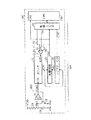
図1は、本発明の第1実施形態の、ワンチップマイクロコンピュータ10Bと周期補正型発振回路に関する外付回路とを示す。
【0024】
コンピュータ10Bは、CPU11Bと、周期補正型発振回路40の一部である周期補正分周回路とを備え、回路40はこの一部と、コンピュータ10Bに外付けされた低精度発振回路30Aとからなる。
【0025】
発振回路30Aは、図6の発振回路30と、回路としては同一であるが、素子定数が異なる。例えば発振回路30の積分回路の時定数が1.0秒であるのに対し、発振回路30Aのそれは1ミリ秒である。シュミットトリガ回路31の出力クロックCLK3は、コンピュータ10B内のカウンタ41のクロック入力端CKに供給される。
【0026】
ワンチップマイクロコンピュータ10B内では、カウンタ41の並列データ出力端が、レジスタ42のデータ入力端及び比較回路43の一方のデータ入力端に接続されている。比較回路43の他方のデータ入力端には、レジスタ42のデータ出力端が接続されている。
【0027】
周期補正型発振回路40は、制御回路として、制御レジスタ44、オアゲート45及びナンドゲート46を備えている。制御レジスタ44は、クリア信号CLR2、イネーブル信号EN及びキャプチャー信号CAPを出力するビットを備えており、これらはそれぞれ、オアゲート45の一方の入力端、ナンドゲート46の一方の入力端及びレジスタ42のクロック入力端CKに接続されている。ナンドゲート46の他方の入力端には、比較回路43の出力端が接続されて、一致信号EQが供給される。ナンドゲート46の出力端はオアゲート45の他方の入力端に接続され、オアゲート45の出力端はカウンタ41のリセット信号入力端RSTに接続され、これにクリア信号CLR1が供給される。
【0028】
CPU11Bは、制御レジスタ44にデータを設定することによりクリア信号CLR2及びイネーブル信号EN及びキャプチャー信号CAPを生成させ、割込信号入力端INTに供給される一致信号EQに応答して割込処理を行なう。制御レジスタ44のクリア信号CLR2及びキャプチャー信号CAPのビット回路はいずれも、‘1’の入力に対しパルスを出力する構成であっても、単なるフリップフロップであってもよい。
【0029】
次に、図2(A)を参照して、上記の如く構成された回路の動作を説明する。
【0030】
CPU11は、制御レジスタ44に対しクリア信号CLR2のパルスを生成させる。このパルスは、オアゲート45を通り、クリア信号CLR1としてカウンタ41のリセット信号入力端RSTに供給され、これによりカウンタ41のカウントCNがゼロクリアされる。
【0031】
CPU11は、クリア信号CLR2のパルスを生成させてから、所定命令実行時間の経過後に、制御レジスタ44に対しキャプチャー信号CAPのパルスを生成させると共に、イネーブル信号ENを高レベルに遷移させる。これにより、カウントCNが参照値RVとしてレジスタ42に保持される。CN=RVであるので、一致信号EQが高レベルとなり、クリア信号CLR1が高レベルとなって、カウンタ41がゼロクリアされる。これにより、一致信号EQが低レベルに遷移し、クリア信号CLR1が低レベルに遷移して、カウンタ41が計数可能となる。
【0032】
クリア信号CLR2及びキャプチャー信号CAPのパルスは、電源投入などによりコンピュータ10Bがリセットされた後、1回のみ生成すればよい。
【0033】
カウントCNが上昇して参照値RVに一致すると、一致信号EQが再度高レベルとなる。すなわち、最初のクリア信号CLR2の立ち上がりからキャプチャー信号CAPの立ち上がりまでの時間が経過する毎に、一致信号EQのパルスが生成される。これは、発振回路30Aの部品精度が低くて製品間でクロックCLK3の周期にばらつきがあっても、これに応じた値がレジスタ42に設定されて、一致信号EQの周期が発振回路30Aの部品精度によらず一定となるからである。この精度は、クロックCLK3の周期をTとすると、±0.75T程度であり、例えばRVが約1000であれば約±0.75T/1000T=±0.075%となる。
【0034】
図2(B)は、図2(A)の場合よりもクロックCLK3の周期が短い場合を示している。
【0035】
図3は、図1の回路の変形例である。
【0036】
この回路では、発振回路30Bがワンチップマイクロコンピュータ10Cに内蔵されて、図1の場合よりも部品点数が少なくなっており、システムを安価に構成することができる。内蔵可能であるのは、抵抗33とキャパシタ34とからなる積分回路の時定数が図6のそれに比し充分小さいからである。
【0037】
[第2実施形態]
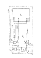
図4は、本発明の第2実施形態の周期補正型発振回路50を示す。
【0038】
この回路50は、図3の周期補正型発振回路40Aを備える共に、周波数逓倍回路51と直列/並列変換回路52とを備えている。
【0039】
周波数逓倍回路51は、一致信号EQを参照クロックとして、周波数がそのN倍のシステムクロックCLKを生成する。システムクロックCLKは、クロックに同期して動作する装置、例えばCPUやその周辺装置の動作クロックとして用いられる。周波数逓倍回路51は、位相比較器53、ローパスフィルタ54、電圧制御発振器55及びプログラマブルN分周回路56が環状接続されたPLL回路であり、位相比較器53は一致信号EQと分周回路56の出力信号の位相とを比較する。
【0040】
直列/並列変換回路52は、周期補正型発振回路50の入力点数を少なくするためのものであり、そのシリアルデータ入力端D及びシフトクロック入力端CKにはそれぞれ外部からシリアルデータSI及びシフトクロックSCKが供給される。直列/並列変換回路52の並列データ出力端は、プログラマブルN分周回路56のN設定データ入力端及び制御レジスタ44のデータ入力端に接続されている。制御レジスタ44のクロック入力端CK及分周回路56のロード信号入力端LDにはそれぞれ、外部からロード信号LD1及びLD2が供給される。
【0041】
次に、上記の如く構成された本第2実施形態の動作を説明する。
【0042】
プログラマブルN分周回路56の値Nを設定するために、シフトクロックSCKに同期してシリアルデータSIが直列/並列変換回路52に供給され、次にロード信号LD2のパルスにより直列/並列変換回路52の内容が値NとしてプログラマブルN分周回路56に設定される。
【0043】
次に、制御レジスタ44に対し上記第1実施形態で述べたデータを設定するために、直列/並列変換回路52にそのデータが設定され、次いでロード信号LD1のパルスによりこれが制御レジスタ44に設定される。
【0044】
本第2実施形態によれば、少ない部品点数で精度の高いタイマ用周期補正型発振回路を構成すると共に、システムクロック生成回路も構成するこができる。
【0045】
なお、本発明には外にも種々の変形例が含まれる。
【0046】
例えば、カウンタ41はダウンカウンタであってもよく、また、その初期化はゼロ以外の所定値であってもよい。
【0047】
イネーブル信号EN及びアンドゲート46を用いずに、一致信号EQを直接、オアゲート45に供給して、常時発振する構成であってもよい。
【図面の簡単な説明】
【図1】本発明の第1実施形態の、ワンチップマイクロコンピュータと周期補正型発振回路に関する外付回路とを示す図である。
【図2】(A)及び(B)はいずれも、図1中の周期補正型発振回路の動作を示すタイムチャートである。
【図3】図1の回路の変形例である。
【図4】本発明の第2実施形態の周期補正型発振回路を示す図である。
【図5】従来の、ワンチップマイクロコンピュータと発振回路に関する外付回路とを示す図である。
【図6】従来の他の、ワンチップマイクロコンピュータと発振回路に関する外付回路とを示す図である。
【図7】図6の回路の動作を示すタイムチャートである。
【符号の説明】
10、10A〜10C ワンチップマイクロコンピュータ
11、11A、11B CPU
12、22、41 カウンタ
13、23、30、30A、30B 発振回路
14、24 ナンドゲート
14A、21 インバータ
15、25、33 抵抗
16、26 クリスタル発振子
17、18、27、28、34 キャパシタ
31 シュミットトリガ回路
32 NMOSトランジスタ
40、40A、50 周期補正型発振回路
41 カウンタ
42 レジスタ
43 比較回路
44 制御レジスタ
45 オアゲート
46 ナンドゲート
51 周波数逓倍回路
52 直列/並列変換回路[0001]
BACKGROUND OF THE INVENTION
The present invention relates to an oscillation circuit having a period correction function used as a timer, a clock generation circuit, and the like, and a period correction frequency dividing circuit that performs the period correction function.
[0002]
[Prior art]
FIG. 5 shows a conventional one-
[0003]
The CPU 11 in the
[0004]
The clocks CLK1 and CLK2 are 4 MHz and 32 kHz, for example, and are generated by the
[0005]
In the
[0006]
In the normal operation mode, the mode signals MOD0 and MOD1 are set to a high level and a low level, respectively, the clock CLK1 operates and the clock CLK2 stops. In the low power consumption mode, the mode signals MOD0 and MOD1 are set to a low level and a high level, respectively, and the clock CLK1 is stopped and the clock CLK2 is operated. The timer (oscillation circuit) composed of the
[0007]
FIG. 6 shows another conventional one-chip microcomputer 10A and an external circuit related to an oscillation circuit.
[0008]
The
[0009]
The
[0010]
The input signal SW1 and the output signal CLK2A of the Schmitt
[0011]
In response to the rise of the clock CLK2A, the
[0012]
The
[0013]
[Problems to be solved by the invention]
However, since the variation in the time constant of the CR integration circuit is relatively large among products, a large variation occurs in the period of the output clock CLK2A of the
[0014]
In view of such problems, an object of the present invention is to provide a period correction type oscillation circuit whose period is highly accurate even when a low precision oscillation circuit is used, and a period correction frequency dividing circuit used therefor. .
[0015]
[Means for solving the problems and their effects]
In the period correction frequency dividing circuit of the first embodiment of the present invention ,
A counter that counts the clock and that is initialized by the activation of the first initialization signal;
A reference register coupled to the counter and holding a count of the counter in response to activation of the capture signal;
A comparison circuit that activates a match signal when the count and the output value of the reference register are equal;
When the second initialization signal is active, or when both the enable signal and the coincidence signal are active, the first initialization signal is activated, and a predetermined time has elapsed since the activation of the second initialization signal. And a control circuit for activating the capture signal;
Have
[0016]
According to this period correction frequency dividing circuit, even if the clock is generated by the low-accuracy oscillation circuit, a coincidence signal having a high period can be obtained as the clock.
[0017]
In the period correction frequency dividing circuit of the second embodiment of the present invention, in the first embodiment,
The control circuit is
A control register including a bit for outputting the second initialization signal, a bit for outputting the enable signal, and a bit for outputting the capture signal;
A logic circuit that activates the first initialization signal when the second initialization signal is active, or when both the enable signal and the coincidence signal are active;
Have
[0018]
In the period correction frequency dividing circuit of the third embodiment of the present invention, in the second embodiment,
It further includes a PLL circuit that receives the coincidence signal and generates a clock having a frequency that is an integral multiple of the reference clock frequency using the coincidence signal as a reference clock.
[0019]
In the period correction type oscillation circuit of the fourth embodiment of the present invention,
An oscillation circuit for generating a clock;
A counter that counts the clock and that is initialized by activation of a first initialization signal;
A reference register coupled to the counter and holding a count of the counter in response to activation of the capture signal;
A comparison circuit that activates a match signal when the count and the output value of the reference register are equal;
When the second initialization signal is active, or when both the enable signal and the coincidence signal are active, the first initialization signal is activated, and a predetermined time has elapsed since the activation of the second initialization signal. And a control circuit for activating the capture signal;
Have
[0020]
In the period correction type oscillation circuit of the fifth embodiment of the present invention, in the fourth embodiment,
The control circuit is
A control register including a bit for outputting the second initialization signal, a bit for outputting the enable signal, and a bit for outputting the capture signal;
A logic circuit that activates the first initialization signal when the second initialization signal is active, or when both the enable signal and the coincidence signal are active;
Have
In the period correction type oscillation circuit of the sixth embodiment of the present invention, in the fifth embodiment,
It further includes a PLL circuit that receives the coincidence signal and generates a clock having a frequency that is an integral multiple of the reference clock frequency using the coincidence signal as a reference clock.
[0021]
Other objects, configurations and effects of the present invention will become apparent from the following description.
[0022]
DETAILED DESCRIPTION OF THE INVENTION
Hereinafter, embodiments of the present invention will be described with reference to the drawings.
[0023]
[First Embodiment]
FIG. 1 shows a one-
[0024]
The
[0025]
The
[0026]
In the one-
[0027]
The period correction
[0028]
The
[0029]
Next, the operation of the circuit configured as described above will be described with reference to FIG.
[0030]
The CPU 11 causes the
[0031]
The CPU 11 generates the pulse of the clear signal CLR2 and then causes the
[0032]
The pulses of the clear signal CLR2 and the capture signal CAP need only be generated once after the
[0033]
When the count CN increases and coincides with the reference value RV, the coincidence signal EQ becomes high level again. That is, a pulse of the coincidence signal EQ is generated each time the time from the rising edge of the first clear signal CLR2 to the rising edge of the capture signal CAP elapses. This is because even when the component accuracy of the
[0034]
FIG. 2B illustrates a case where the cycle of the clock CLK3 is shorter than that in FIG.
[0035]
FIG. 3 is a modification of the circuit of FIG.
[0036]
In this circuit, the
[0037]
[Second Embodiment]
FIG. 4 shows a period correction
[0038]
The
[0039]
The
[0040]
The serial /
[0041]
Next, the operation of the second embodiment configured as described above will be described.
[0042]
In order to set the value N of the programmable N
[0043]
Next, in order to set the data described in the first embodiment in the
[0044]
According to the second embodiment, it is possible to configure a timer period correction type oscillation circuit with high accuracy with a small number of parts, and also to configure a system clock generation circuit.
[0045]
Note that the present invention includes various other modifications.
[0046]
For example, the
[0047]
Instead of using the enable signal EN and the AND
[Brief description of the drawings]
FIG. 1 is a diagram illustrating a one-chip microcomputer and an external circuit related to a period correction type oscillation circuit according to a first embodiment of the present invention.
FIGS. 2A and 2B are time charts showing the operation of the period correction type oscillation circuit in FIG.
FIG. 3 is a modification of the circuit of FIG.
FIG. 4 is a diagram showing a period correction type oscillation circuit according to a second embodiment of the present invention.
FIG. 5 is a diagram showing a conventional one-chip microcomputer and an external circuit related to an oscillation circuit.
FIG. 6 is a diagram showing another conventional one-chip microcomputer and an external circuit related to an oscillation circuit.
7 is a time chart showing the operation of the circuit of FIG.
[Explanation of symbols]
10, 10A-10C One-
12, 22, 41
Claims (6)
該カウンタに結合され、キャプチャ信号の活性化に応答して該カウンタのカウントを保持する参照レジスタと、
該カウントと該参照レジスタの出力値とが等しくなった時に、一致信号を活性化する比較回路と、
第2初期化信号が活性であるとき、又は、イネーブル信号及び該一致信号が共に活性であるときに、該第1初期化信号を活性化し、該第2初期化信号の活性化から所定時間経過した後に、該キャプチャ信号を活性化する制御回路と、
を有することを特徴とする周期補正分周回路。A counter that counts the clock and that is initialized by the activation of the first initialization signal;
A reference register coupled to the counter and holding a count of the counter in response to activation of the capture signal;
A comparison circuit that activates a match signal when the count and the output value of the reference register are equal;
When the second initialization signal is active, or when both the enable signal and the coincidence signal are active, the first initialization signal is activated, and a predetermined time has elapsed since the activation of the second initialization signal. And a control circuit for activating the capture signal;
And a period correction frequency dividing circuit.
上記第2初期化信号を出力するビットと、上記イネーブル信号を出力するビットと、上記キャプチャ信号を出力するビットとを含む制御レジスタと、
上記第2初期化信号が活性であるとき、又は、上記イネーブル信号及び上記一致信号が共に活性であるときに、上記第1初期化信号を活性化する論理回路と、
を有することを特徴とする請求項1記載の周期補正分周回路。 The control circuit is
A control register including a bit for outputting the second initialization signal, a bit for outputting the enable signal, and a bit for outputting the capture signal;
A logic circuit that activates the first initialization signal when the second initialization signal is active, or when both the enable signal and the coincidence signal are active;
The period correction frequency dividing circuit according to claim 1, further comprising:
該クロックをカウントし、第1初期化信号の活性化により該カウントが初期化されるカウンタと、
該カウンタに結合され、キャプチャ信号の活性化に応答して該カウンタのカウントを保持する参照レジスタと、
該カウントと該参照レジスタの出力値とが等しくなった時に、一致信号を活性化する比較回路と、
第2初期化信号が活性であるとき、又は、イネーブル信号及び該一致信号が共に活性であるときに、該第1初期化信号を活性化し、該第2初期化信号の活性化から所定時間経過した後に、該キャプチャ信号を活性化する制御回路と、
を有することを特徴とする周期補正型発振回路。 An oscillation circuit for generating a clock;
Counting the clock, a counter for the count is initialized by the activation of the first initialization signal,
A reference register coupled to the counter and holding a count of the counter in response to activation of the capture signal;
When the output value of said count and said reference register is equal, the comparison circuit activates No. one match signal,
When the second initialization signal is active, or when both the enable signal and the coincidence signal are active, the first initialization signal is activated, and a predetermined time has elapsed since the activation of the second initialization signal. And a control circuit for activating the capture signal;
A period-corrected oscillation circuit comprising:
上記第2初期化信号を出力するビットと、上記イネーブル信号を出力するビットと、上記キャプチャ信号を出力するビットとを含む制御レジスタと、
上記第2初期化信号が活性であるとき、又は、上記イネーブル信号及び上記一致信号が共に活性であるときに、上記第1初期化信号を活性化する論理回路と、
を有することを特徴とする請求項4記載の周期補正型発振回路。The control circuit is
A control register including a bit for outputting the second initialization signal, a bit for outputting the enable signal, and a bit for outputting the capture signal;
A logic circuit that activates the first initialization signal when the second initialization signal is active, or when both the enable signal and the coincidence signal are active;
The period-correcting oscillation circuit according to claim 4, wherein:
Priority Applications (2)
| Application Number | Priority Date | Filing Date | Title |
|---|---|---|---|
| JP23375899A JP4111636B2 (en) | 1999-08-20 | 1999-08-20 | Period correction frequency dividing circuit and period correction type oscillation circuit using the same |
| US09/640,723 US6486717B2 (en) | 1999-08-20 | 2000-08-18 | Divider with cycle time correction |
Applications Claiming Priority (1)
| Application Number | Priority Date | Filing Date | Title |
|---|---|---|---|
| JP23375899A JP4111636B2 (en) | 1999-08-20 | 1999-08-20 | Period correction frequency dividing circuit and period correction type oscillation circuit using the same |
Publications (3)
| Publication Number | Publication Date |
|---|---|
| JP2001060851A JP2001060851A (en) | 2001-03-06 |
| JP2001060851A5 JP2001060851A5 (en) | 2006-08-31 |
| JP4111636B2 true JP4111636B2 (en) | 2008-07-02 |
Family
ID=16960126
Family Applications (1)
| Application Number | Title | Priority Date | Filing Date |
|---|---|---|---|
| JP23375899A Expired - Fee Related JP4111636B2 (en) | 1999-08-20 | 1999-08-20 | Period correction frequency dividing circuit and period correction type oscillation circuit using the same |
Country Status (2)
| Country | Link |
|---|---|
| US (1) | US6486717B2 (en) |
| JP (1) | JP4111636B2 (en) |
Families Citing this family (5)
| Publication number | Priority date | Publication date | Assignee | Title |
|---|---|---|---|---|
| US7321651B2 (en) * | 2004-11-12 | 2008-01-22 | International Business Machines Corporation | High frequency circuit capable of error detection and correction of code patterns running at full speed |
| KR101162259B1 (en) * | 2010-12-03 | 2012-07-04 | 에스케이하이닉스 주식회사 | Semiconductor integrated circuit and a method of driving the semiconductor integrated circuit |
| JP2013038744A (en) * | 2011-08-11 | 2013-02-21 | Renesas Electronics Corp | Oscillation circuit and semiconductor integrated circuit having the same |
| US8754690B2 (en) * | 2012-10-26 | 2014-06-17 | International Business Machines Corporation | Programmable duty cycle setter employing time to voltage domain referenced pulse creation |
| US10637448B1 (en) * | 2019-06-03 | 2020-04-28 | Texas Instruments Incorporated | Low-power high-speed Schmitt Trigger with high noise rejection |
Family Cites Families (6)
| Publication number | Priority date | Publication date | Assignee | Title |
|---|---|---|---|---|
| US3836858A (en) * | 1971-06-30 | 1974-09-17 | Nippon Denso Co | Pulse width setting apparatus |
| JPS5983254A (en) * | 1982-11-04 | 1984-05-14 | Oki Electric Ind Co Ltd | Watchdog timer |
| JP3322893B2 (en) * | 1991-09-30 | 2002-09-09 | エヌイーシーマイクロシステム株式会社 | Microcomputer |
| KR970010638B1 (en) * | 1994-05-11 | 1997-06-28 | 삼성전자 주식회사 | Servo-address mark detection and compensation circuit |
| JPH1117528A (en) * | 1997-06-23 | 1999-01-22 | Mitsubishi Electric Corp | Output timer |
| JP3082721B2 (en) * | 1997-09-19 | 2000-08-28 | 日本電気株式会社 | Timer device |
-
1999
- 1999-08-20 JP JP23375899A patent/JP4111636B2/en not_active Expired - Fee Related
-
2000
- 2000-08-18 US US09/640,723 patent/US6486717B2/en not_active Expired - Lifetime
Also Published As
| Publication number | Publication date |
|---|---|
| US20020063591A1 (en) | 2002-05-30 |
| JP2001060851A (en) | 2001-03-06 |
| US6486717B2 (en) | 2002-11-26 |
Similar Documents
| Publication | Publication Date | Title |
|---|---|---|
| JP3023238B2 (en) | Power-on reset system and semiconductor memory device provided with the power-on reset system | |
| JP4725418B2 (en) | Time measurement circuit | |
| JP2001238435A (en) | Voltage-transforming circuit | |
| EP0590607B1 (en) | Low-power baud rate generator | |
| JP4111636B2 (en) | Period correction frequency dividing circuit and period correction type oscillation circuit using the same | |
| US10020815B2 (en) | Apparatus for data converter with internal trigger circuitry and associated methods | |
| JP3944226B2 (en) | Backup circuit | |
| EP0840956A1 (en) | Microcontroller having a minimal number of external components | |
| JPH1198007A (en) | Frequency divider | |
| JP3105510B2 (en) | Semiconductor integrated circuit | |
| US9362894B1 (en) | Clock generator circuit | |
| TWI382301B (en) | Control circuit for power-on-reset and its operating method | |
| JP4122128B2 (en) | Edge detection circuit | |
| JPS5828608B2 (en) | arithmetic processing unit | |
| JP2556038B2 (en) | Hybrid integrated circuit | |
| TW202410030A (en) | Monitoring circuits and storage systems | |
| JP2723741B2 (en) | Clock generation circuit for semiconductor integrated circuit | |
| JPS5936767B2 (en) | Auto clear circuit system | |
| JP2722348B2 (en) | Oscillation circuit | |
| JP2000194435A (en) | Stabilized oscillation detecting circuit, clock signal oscillator, and stabilized oscillation detecting method | |
| JPS5935219A (en) | Resetting circuit | |
| JPH07106926A (en) | Clock generating circuit and data processor | |
| JPS6035902Y2 (en) | Unadjusted battery life detection circuit | |
| KR100468678B1 (en) | System Clock Generator and Method | |
| JPS6349949Y2 (en) |
Legal Events
| Date | Code | Title | Description |
|---|---|---|---|
| A521 | Request for written amendment filed |
Free format text: JAPANESE INTERMEDIATE CODE: A523 Effective date: 20060710 |
|
| A621 | Written request for application examination |
Free format text: JAPANESE INTERMEDIATE CODE: A621 Effective date: 20060710 |
|
| A977 | Report on retrieval |
Free format text: JAPANESE INTERMEDIATE CODE: A971007 Effective date: 20071016 |
|
| A131 | Notification of reasons for refusal |
Free format text: JAPANESE INTERMEDIATE CODE: A131 Effective date: 20071113 |
|
| TRDD | Decision of grant or rejection written | ||
| A01 | Written decision to grant a patent or to grant a registration (utility model) |
Free format text: JAPANESE INTERMEDIATE CODE: A01 Effective date: 20080408 |
|
| A61 | First payment of annual fees (during grant procedure) |
Free format text: JAPANESE INTERMEDIATE CODE: A61 Effective date: 20080408 |
|
| R150 | Certificate of patent or registration of utility model |
Free format text: JAPANESE INTERMEDIATE CODE: R150 |
|
| FPAY | Renewal fee payment (event date is renewal date of database) |
Free format text: PAYMENT UNTIL: 20110418 Year of fee payment: 3 |
|
| S111 | Request for change of ownership or part of ownership |
Free format text: JAPANESE INTERMEDIATE CODE: R313111 |
|
| FPAY | Renewal fee payment (event date is renewal date of database) |
Free format text: PAYMENT UNTIL: 20110418 Year of fee payment: 3 |
|
| R350 | Written notification of registration of transfer |
Free format text: JAPANESE INTERMEDIATE CODE: R350 |
|
| FPAY | Renewal fee payment (event date is renewal date of database) |
Free format text: PAYMENT UNTIL: 20110418 Year of fee payment: 3 |
|
| S531 | Written request for registration of change of domicile |
Free format text: JAPANESE INTERMEDIATE CODE: R313531 |
|
| S533 | Written request for registration of change of name |
Free format text: JAPANESE INTERMEDIATE CODE: R313533 |
|
| FPAY | Renewal fee payment (event date is renewal date of database) |
Free format text: PAYMENT UNTIL: 20110418 Year of fee payment: 3 |
|
| R350 | Written notification of registration of transfer |
Free format text: JAPANESE INTERMEDIATE CODE: R350 |
|
| FPAY | Renewal fee payment (event date is renewal date of database) |
Free format text: PAYMENT UNTIL: 20120418 Year of fee payment: 4 |
|
| FPAY | Renewal fee payment (event date is renewal date of database) |
Free format text: PAYMENT UNTIL: 20130418 Year of fee payment: 5 |
|
| FPAY | Renewal fee payment (event date is renewal date of database) |
Free format text: PAYMENT UNTIL: 20130418 Year of fee payment: 5 |
|
| FPAY | Renewal fee payment (event date is renewal date of database) |
Free format text: PAYMENT UNTIL: 20140418 Year of fee payment: 6 |
|
| S111 | Request for change of ownership or part of ownership |
Free format text: JAPANESE INTERMEDIATE CODE: R313111 |
|
| R350 | Written notification of registration of transfer |
Free format text: JAPANESE INTERMEDIATE CODE: R350 |
|
| LAPS | Cancellation because of no payment of annual fees |