JP4095827B2 - Semiconductor device - Google Patents
Semiconductor device Download PDFInfo
- Publication number
- JP4095827B2 JP4095827B2 JP2002134952A JP2002134952A JP4095827B2 JP 4095827 B2 JP4095827 B2 JP 4095827B2 JP 2002134952 A JP2002134952 A JP 2002134952A JP 2002134952 A JP2002134952 A JP 2002134952A JP 4095827 B2 JP4095827 B2 JP 4095827B2
- Authority
- JP
- Japan
- Prior art keywords
- lead
- sealing body
- lead frame
- qfn
- semiconductor device
- Prior art date
- Legal status (The legal status is an assumption and is not a legal conclusion. Google has not performed a legal analysis and makes no representation as to the accuracy of the status listed.)
- Expired - Fee Related
Links
- 239000004065 semiconductor Substances 0.000 title claims abstract description 96
- 238000007789 sealing Methods 0.000 claims abstract description 69
- 239000000725 suspension Substances 0.000 claims abstract description 44
- 238000005452 bending Methods 0.000 claims description 5
- 238000004519 manufacturing process Methods 0.000 abstract description 37
- 239000002184 metal Substances 0.000 abstract description 22
- 229910052751 metal Inorganic materials 0.000 abstract description 22
- 238000005530 etching Methods 0.000 abstract description 9
- 238000003825 pressing Methods 0.000 abstract description 4
- 238000000034 method Methods 0.000 description 35
- 229920005989 resin Polymers 0.000 description 23
- 239000011347 resin Substances 0.000 description 23
- 229920002120 photoresistant polymer Polymers 0.000 description 15
- 229910000679 solder Inorganic materials 0.000 description 15
- 238000000465 moulding Methods 0.000 description 10
- 238000007747 plating Methods 0.000 description 5
- 238000007639 printing Methods 0.000 description 5
- 229910000881 Cu alloy Inorganic materials 0.000 description 3
- 229910001030 Iron–nickel alloy Inorganic materials 0.000 description 3
- 229910045601 alloy Inorganic materials 0.000 description 3
- 239000000956 alloy Substances 0.000 description 3
- 229910052802 copper Inorganic materials 0.000 description 3
- 238000006073 displacement reaction Methods 0.000 description 3
- 238000005476 soldering Methods 0.000 description 3
- 239000000853 adhesive Substances 0.000 description 2
- 230000001070 adhesive effect Effects 0.000 description 2
- 230000000694 effects Effects 0.000 description 2
- 238000009713 electroplating Methods 0.000 description 2
- 238000010438 heat treatment Methods 0.000 description 2
- 230000000873 masking effect Effects 0.000 description 2
- 230000003287 optical effect Effects 0.000 description 2
- 238000004080 punching Methods 0.000 description 2
- 239000000126 substance Substances 0.000 description 2
- 239000000758 substrate Substances 0.000 description 2
- 229920003002 synthetic resin Polymers 0.000 description 2
- 239000000057 synthetic resin Substances 0.000 description 2
- 230000015572 biosynthetic process Effects 0.000 description 1
- 239000004020 conductor Substances 0.000 description 1
- 238000005260 corrosion Methods 0.000 description 1
- 230000007797 corrosion Effects 0.000 description 1
- 238000005520 cutting process Methods 0.000 description 1
- 238000005516 engineering process Methods 0.000 description 1
- 239000003822 epoxy resin Substances 0.000 description 1
- 239000011888 foil Substances 0.000 description 1
- 239000003292 glue Substances 0.000 description 1
- 238000012986 modification Methods 0.000 description 1
- 230000004048 modification Effects 0.000 description 1
- 230000002093 peripheral effect Effects 0.000 description 1
- 229920000647 polyepoxide Polymers 0.000 description 1
- 230000003252 repetitive effect Effects 0.000 description 1
- 230000000630 rising effect Effects 0.000 description 1
- 238000007650 screen-printing Methods 0.000 description 1
Images


Classifications
-
- H—ELECTRICITY
- H01—ELECTRIC ELEMENTS
- H01L—SEMICONDUCTOR DEVICES NOT COVERED BY CLASS H10
- H01L21/00—Processes or apparatus adapted for the manufacture or treatment of semiconductor or solid state devices or of parts thereof
- H01L21/02—Manufacture or treatment of semiconductor devices or of parts thereof
- H01L21/04—Manufacture or treatment of semiconductor devices or of parts thereof the devices having potential barriers, e.g. a PN junction, depletion layer or carrier concentration layer
- H01L21/50—Assembly of semiconductor devices using processes or apparatus not provided for in a single one of the subgroups H01L21/06 - H01L21/326, e.g. sealing of a cap to a base of a container
- H01L21/56—Encapsulations, e.g. encapsulation layers, coatings
- H01L21/561—Batch processing
-
- H—ELECTRICITY
- H01—ELECTRIC ELEMENTS
- H01L—SEMICONDUCTOR DEVICES NOT COVERED BY CLASS H10
- H01L23/00—Details of semiconductor or other solid state devices
- H01L23/52—Arrangements for conducting electric current within the device in operation from one component to another, i.e. interconnections, e.g. wires, lead frames
-
- H—ELECTRICITY
- H01—ELECTRIC ELEMENTS
- H01L—SEMICONDUCTOR DEVICES NOT COVERED BY CLASS H10
- H01L21/00—Processes or apparatus adapted for the manufacture or treatment of semiconductor or solid state devices or of parts thereof
- H01L21/02—Manufacture or treatment of semiconductor devices or of parts thereof
- H01L21/04—Manufacture or treatment of semiconductor devices or of parts thereof the devices having potential barriers, e.g. a PN junction, depletion layer or carrier concentration layer
- H01L21/48—Manufacture or treatment of parts, e.g. containers, prior to assembly of the devices, using processes not provided for in a single one of the subgroups H01L21/06 - H01L21/326
- H01L21/4814—Conductive parts
- H01L21/4821—Flat leads, e.g. lead frames with or without insulating supports
- H01L21/4828—Etching
-
- H—ELECTRICITY
- H01—ELECTRIC ELEMENTS
- H01L—SEMICONDUCTOR DEVICES NOT COVERED BY CLASS H10
- H01L21/00—Processes or apparatus adapted for the manufacture or treatment of semiconductor or solid state devices or of parts thereof
- H01L21/02—Manufacture or treatment of semiconductor devices or of parts thereof
- H01L21/04—Manufacture or treatment of semiconductor devices or of parts thereof the devices having potential barriers, e.g. a PN junction, depletion layer or carrier concentration layer
- H01L21/50—Assembly of semiconductor devices using processes or apparatus not provided for in a single one of the subgroups H01L21/06 - H01L21/326, e.g. sealing of a cap to a base of a container
- H01L21/56—Encapsulations, e.g. encapsulation layers, coatings
- H01L21/565—Moulds
-
- H—ELECTRICITY
- H01—ELECTRIC ELEMENTS
- H01L—SEMICONDUCTOR DEVICES NOT COVERED BY CLASS H10
- H01L23/00—Details of semiconductor or other solid state devices
- H01L23/28—Encapsulations, e.g. encapsulating layers, coatings, e.g. for protection
- H01L23/31—Encapsulations, e.g. encapsulating layers, coatings, e.g. for protection characterised by the arrangement or shape
- H01L23/3107—Encapsulations, e.g. encapsulating layers, coatings, e.g. for protection characterised by the arrangement or shape the device being completely enclosed
-
- H—ELECTRICITY
- H01—ELECTRIC ELEMENTS
- H01L—SEMICONDUCTOR DEVICES NOT COVERED BY CLASS H10
- H01L23/00—Details of semiconductor or other solid state devices
- H01L23/48—Arrangements for conducting electric current to or from the solid state body in operation, e.g. leads, terminal arrangements ; Selection of materials therefor
- H01L23/488—Arrangements for conducting electric current to or from the solid state body in operation, e.g. leads, terminal arrangements ; Selection of materials therefor consisting of soldered or bonded constructions
- H01L23/495—Lead-frames or other flat leads
- H01L23/49503—Lead-frames or other flat leads characterised by the die pad
- H01L23/49506—Lead-frames or other flat leads characterised by the die pad an insulative substrate being used as a diepad, e.g. ceramic, plastic
-
- H—ELECTRICITY
- H01—ELECTRIC ELEMENTS
- H01L—SEMICONDUCTOR DEVICES NOT COVERED BY CLASS H10
- H01L23/00—Details of semiconductor or other solid state devices
- H01L23/48—Arrangements for conducting electric current to or from the solid state body in operation, e.g. leads, terminal arrangements ; Selection of materials therefor
- H01L23/488—Arrangements for conducting electric current to or from the solid state body in operation, e.g. leads, terminal arrangements ; Selection of materials therefor consisting of soldered or bonded constructions
- H01L23/495—Lead-frames or other flat leads
- H01L23/49541—Geometry of the lead-frame
- H01L23/49548—Cross section geometry
-
- H—ELECTRICITY
- H01—ELECTRIC ELEMENTS
- H01L—SEMICONDUCTOR DEVICES NOT COVERED BY CLASS H10
- H01L23/00—Details of semiconductor or other solid state devices
- H01L23/544—Marks applied to semiconductor devices or parts, e.g. registration marks, alignment structures, wafer maps
-
- H—ELECTRICITY
- H01—ELECTRIC ELEMENTS
- H01L—SEMICONDUCTOR DEVICES NOT COVERED BY CLASS H10
- H01L24/00—Arrangements for connecting or disconnecting semiconductor or solid-state bodies; Methods or apparatus related thereto
- H01L24/74—Apparatus for manufacturing arrangements for connecting or disconnecting semiconductor or solid-state bodies
- H01L24/78—Apparatus for connecting with wire connectors
-
- H—ELECTRICITY
- H01—ELECTRIC ELEMENTS
- H01L—SEMICONDUCTOR DEVICES NOT COVERED BY CLASS H10
- H01L24/00—Arrangements for connecting or disconnecting semiconductor or solid-state bodies; Methods or apparatus related thereto
- H01L24/80—Methods for connecting semiconductor or other solid state bodies using means for bonding being attached to, or being formed on, the surface to be connected
- H01L24/85—Methods for connecting semiconductor or other solid state bodies using means for bonding being attached to, or being formed on, the surface to be connected using a wire connector
-
- H—ELECTRICITY
- H01—ELECTRIC ELEMENTS
- H01L—SEMICONDUCTOR DEVICES NOT COVERED BY CLASS H10
- H01L24/00—Arrangements for connecting or disconnecting semiconductor or solid-state bodies; Methods or apparatus related thereto
- H01L24/93—Batch processes
- H01L24/95—Batch processes at chip-level, i.e. with connecting carried out on a plurality of singulated devices, i.e. on diced chips
- H01L24/97—Batch processes at chip-level, i.e. with connecting carried out on a plurality of singulated devices, i.e. on diced chips the devices being connected to a common substrate, e.g. interposer, said common substrate being separable into individual assemblies after connecting
-
- H—ELECTRICITY
- H01—ELECTRIC ELEMENTS
- H01L—SEMICONDUCTOR DEVICES NOT COVERED BY CLASS H10
- H01L2223/00—Details relating to semiconductor or other solid state devices covered by the group H01L23/00
- H01L2223/544—Marks applied to semiconductor devices or parts
- H01L2223/54473—Marks applied to semiconductor devices or parts for use after dicing
-
- H—ELECTRICITY
- H01—ELECTRIC ELEMENTS
- H01L—SEMICONDUCTOR DEVICES NOT COVERED BY CLASS H10
- H01L2224/00—Indexing scheme for arrangements for connecting or disconnecting semiconductor or solid-state bodies and methods related thereto as covered by H01L24/00
- H01L2224/01—Means for bonding being attached to, or being formed on, the surface to be connected, e.g. chip-to-package, die-attach, "first-level" interconnects; Manufacturing methods related thereto
- H01L2224/02—Bonding areas; Manufacturing methods related thereto
- H01L2224/04—Structure, shape, material or disposition of the bonding areas prior to the connecting process
- H01L2224/05—Structure, shape, material or disposition of the bonding areas prior to the connecting process of an individual bonding area
- H01L2224/0554—External layer
- H01L2224/0555—Shape
- H01L2224/05552—Shape in top view
- H01L2224/05554—Shape in top view being square
-
- H—ELECTRICITY
- H01—ELECTRIC ELEMENTS
- H01L—SEMICONDUCTOR DEVICES NOT COVERED BY CLASS H10
- H01L2224/00—Indexing scheme for arrangements for connecting or disconnecting semiconductor or solid-state bodies and methods related thereto as covered by H01L24/00
- H01L2224/01—Means for bonding being attached to, or being formed on, the surface to be connected, e.g. chip-to-package, die-attach, "first-level" interconnects; Manufacturing methods related thereto
- H01L2224/26—Layer connectors, e.g. plate connectors, solder or adhesive layers; Manufacturing methods related thereto
- H01L2224/31—Structure, shape, material or disposition of the layer connectors after the connecting process
- H01L2224/32—Structure, shape, material or disposition of the layer connectors after the connecting process of an individual layer connector
- H01L2224/3201—Structure
- H01L2224/32012—Structure relative to the bonding area, e.g. bond pad
- H01L2224/32014—Structure relative to the bonding area, e.g. bond pad the layer connector being smaller than the bonding area, e.g. bond pad
-
- H—ELECTRICITY
- H01—ELECTRIC ELEMENTS
- H01L—SEMICONDUCTOR DEVICES NOT COVERED BY CLASS H10
- H01L2224/00—Indexing scheme for arrangements for connecting or disconnecting semiconductor or solid-state bodies and methods related thereto as covered by H01L24/00
- H01L2224/01—Means for bonding being attached to, or being formed on, the surface to be connected, e.g. chip-to-package, die-attach, "first-level" interconnects; Manufacturing methods related thereto
- H01L2224/26—Layer connectors, e.g. plate connectors, solder or adhesive layers; Manufacturing methods related thereto
- H01L2224/31—Structure, shape, material or disposition of the layer connectors after the connecting process
- H01L2224/32—Structure, shape, material or disposition of the layer connectors after the connecting process of an individual layer connector
- H01L2224/3205—Shape
- H01L2224/32052—Shape in top view
- H01L2224/32055—Shape in top view being circular or elliptic
-
- H—ELECTRICITY
- H01—ELECTRIC ELEMENTS
- H01L—SEMICONDUCTOR DEVICES NOT COVERED BY CLASS H10
- H01L2224/00—Indexing scheme for arrangements for connecting or disconnecting semiconductor or solid-state bodies and methods related thereto as covered by H01L24/00
- H01L2224/01—Means for bonding being attached to, or being formed on, the surface to be connected, e.g. chip-to-package, die-attach, "first-level" interconnects; Manufacturing methods related thereto
- H01L2224/26—Layer connectors, e.g. plate connectors, solder or adhesive layers; Manufacturing methods related thereto
- H01L2224/31—Structure, shape, material or disposition of the layer connectors after the connecting process
- H01L2224/32—Structure, shape, material or disposition of the layer connectors after the connecting process of an individual layer connector
- H01L2224/321—Disposition
- H01L2224/32151—Disposition the layer connector connecting between a semiconductor or solid-state body and an item not being a semiconductor or solid-state body, e.g. chip-to-substrate, chip-to-passive
- H01L2224/32221—Disposition the layer connector connecting between a semiconductor or solid-state body and an item not being a semiconductor or solid-state body, e.g. chip-to-substrate, chip-to-passive the body and the item being stacked
- H01L2224/32245—Disposition the layer connector connecting between a semiconductor or solid-state body and an item not being a semiconductor or solid-state body, e.g. chip-to-substrate, chip-to-passive the body and the item being stacked the item being metallic
-
- H—ELECTRICITY
- H01—ELECTRIC ELEMENTS
- H01L—SEMICONDUCTOR DEVICES NOT COVERED BY CLASS H10
- H01L2224/00—Indexing scheme for arrangements for connecting or disconnecting semiconductor or solid-state bodies and methods related thereto as covered by H01L24/00
- H01L2224/01—Means for bonding being attached to, or being formed on, the surface to be connected, e.g. chip-to-package, die-attach, "first-level" interconnects; Manufacturing methods related thereto
- H01L2224/42—Wire connectors; Manufacturing methods related thereto
- H01L2224/44—Structure, shape, material or disposition of the wire connectors prior to the connecting process
- H01L2224/45—Structure, shape, material or disposition of the wire connectors prior to the connecting process of an individual wire connector
- H01L2224/45001—Core members of the connector
- H01L2224/4501—Shape
- H01L2224/45012—Cross-sectional shape
- H01L2224/45015—Cross-sectional shape being circular
-
- H—ELECTRICITY
- H01—ELECTRIC ELEMENTS
- H01L—SEMICONDUCTOR DEVICES NOT COVERED BY CLASS H10
- H01L2224/00—Indexing scheme for arrangements for connecting or disconnecting semiconductor or solid-state bodies and methods related thereto as covered by H01L24/00
- H01L2224/01—Means for bonding being attached to, or being formed on, the surface to be connected, e.g. chip-to-package, die-attach, "first-level" interconnects; Manufacturing methods related thereto
- H01L2224/42—Wire connectors; Manufacturing methods related thereto
- H01L2224/44—Structure, shape, material or disposition of the wire connectors prior to the connecting process
- H01L2224/45—Structure, shape, material or disposition of the wire connectors prior to the connecting process of an individual wire connector
- H01L2224/45001—Core members of the connector
- H01L2224/45099—Material
- H01L2224/451—Material with a principal constituent of the material being a metal or a metalloid, e.g. boron (B), silicon (Si), germanium (Ge), arsenic (As), antimony (Sb), tellurium (Te) and polonium (Po), and alloys thereof
- H01L2224/45138—Material with a principal constituent of the material being a metal or a metalloid, e.g. boron (B), silicon (Si), germanium (Ge), arsenic (As), antimony (Sb), tellurium (Te) and polonium (Po), and alloys thereof the principal constituent melting at a temperature of greater than or equal to 950°C and less than 1550°C
- H01L2224/45144—Gold (Au) as principal constituent
-
- H—ELECTRICITY
- H01—ELECTRIC ELEMENTS
- H01L—SEMICONDUCTOR DEVICES NOT COVERED BY CLASS H10
- H01L2224/00—Indexing scheme for arrangements for connecting or disconnecting semiconductor or solid-state bodies and methods related thereto as covered by H01L24/00
- H01L2224/01—Means for bonding being attached to, or being formed on, the surface to be connected, e.g. chip-to-package, die-attach, "first-level" interconnects; Manufacturing methods related thereto
- H01L2224/42—Wire connectors; Manufacturing methods related thereto
- H01L2224/47—Structure, shape, material or disposition of the wire connectors after the connecting process
- H01L2224/48—Structure, shape, material or disposition of the wire connectors after the connecting process of an individual wire connector
- H01L2224/4805—Shape
- H01L2224/4809—Loop shape
- H01L2224/48091—Arched
-
- H—ELECTRICITY
- H01—ELECTRIC ELEMENTS
- H01L—SEMICONDUCTOR DEVICES NOT COVERED BY CLASS H10
- H01L2224/00—Indexing scheme for arrangements for connecting or disconnecting semiconductor or solid-state bodies and methods related thereto as covered by H01L24/00
- H01L2224/01—Means for bonding being attached to, or being formed on, the surface to be connected, e.g. chip-to-package, die-attach, "first-level" interconnects; Manufacturing methods related thereto
- H01L2224/42—Wire connectors; Manufacturing methods related thereto
- H01L2224/47—Structure, shape, material or disposition of the wire connectors after the connecting process
- H01L2224/48—Structure, shape, material or disposition of the wire connectors after the connecting process of an individual wire connector
- H01L2224/481—Disposition
- H01L2224/48151—Connecting between a semiconductor or solid-state body and an item not being a semiconductor or solid-state body, e.g. chip-to-substrate, chip-to-passive
- H01L2224/48221—Connecting between a semiconductor or solid-state body and an item not being a semiconductor or solid-state body, e.g. chip-to-substrate, chip-to-passive the body and the item being stacked
- H01L2224/48245—Connecting between a semiconductor or solid-state body and an item not being a semiconductor or solid-state body, e.g. chip-to-substrate, chip-to-passive the body and the item being stacked the item being metallic
- H01L2224/48247—Connecting between a semiconductor or solid-state body and an item not being a semiconductor or solid-state body, e.g. chip-to-substrate, chip-to-passive the body and the item being stacked the item being metallic connecting the wire to a bond pad of the item
-
- H—ELECTRICITY
- H01—ELECTRIC ELEMENTS
- H01L—SEMICONDUCTOR DEVICES NOT COVERED BY CLASS H10
- H01L2224/00—Indexing scheme for arrangements for connecting or disconnecting semiconductor or solid-state bodies and methods related thereto as covered by H01L24/00
- H01L2224/01—Means for bonding being attached to, or being formed on, the surface to be connected, e.g. chip-to-package, die-attach, "first-level" interconnects; Manufacturing methods related thereto
- H01L2224/42—Wire connectors; Manufacturing methods related thereto
- H01L2224/47—Structure, shape, material or disposition of the wire connectors after the connecting process
- H01L2224/49—Structure, shape, material or disposition of the wire connectors after the connecting process of a plurality of wire connectors
- H01L2224/491—Disposition
- H01L2224/4912—Layout
- H01L2224/49171—Fan-out arrangements
-
- H—ELECTRICITY
- H01—ELECTRIC ELEMENTS
- H01L—SEMICONDUCTOR DEVICES NOT COVERED BY CLASS H10
- H01L2224/00—Indexing scheme for arrangements for connecting or disconnecting semiconductor or solid-state bodies and methods related thereto as covered by H01L24/00
- H01L2224/73—Means for bonding being of different types provided for in two or more of groups H01L2224/10, H01L2224/18, H01L2224/26, H01L2224/34, H01L2224/42, H01L2224/50, H01L2224/63, H01L2224/71
- H01L2224/732—Location after the connecting process
- H01L2224/73251—Location after the connecting process on different surfaces
- H01L2224/73265—Layer and wire connectors
-
- H—ELECTRICITY
- H01—ELECTRIC ELEMENTS
- H01L—SEMICONDUCTOR DEVICES NOT COVERED BY CLASS H10
- H01L2224/00—Indexing scheme for arrangements for connecting or disconnecting semiconductor or solid-state bodies and methods related thereto as covered by H01L24/00
- H01L2224/74—Apparatus for manufacturing arrangements for connecting or disconnecting semiconductor or solid-state bodies and for methods related thereto
- H01L2224/78—Apparatus for connecting with wire connectors
- H01L2224/7825—Means for applying energy, e.g. heating means
- H01L2224/783—Means for applying energy, e.g. heating means by means of pressure
- H01L2224/78301—Capillary
-
- H—ELECTRICITY
- H01—ELECTRIC ELEMENTS
- H01L—SEMICONDUCTOR DEVICES NOT COVERED BY CLASS H10
- H01L2224/00—Indexing scheme for arrangements for connecting or disconnecting semiconductor or solid-state bodies and methods related thereto as covered by H01L24/00
- H01L2224/74—Apparatus for manufacturing arrangements for connecting or disconnecting semiconductor or solid-state bodies and for methods related thereto
- H01L2224/78—Apparatus for connecting with wire connectors
- H01L2224/787—Means for aligning
- H01L2224/78703—Mechanical holding means
-
- H—ELECTRICITY
- H01—ELECTRIC ELEMENTS
- H01L—SEMICONDUCTOR DEVICES NOT COVERED BY CLASS H10
- H01L2224/00—Indexing scheme for arrangements for connecting or disconnecting semiconductor or solid-state bodies and methods related thereto as covered by H01L24/00
- H01L2224/80—Methods for connecting semiconductor or other solid state bodies using means for bonding being attached to, or being formed on, the surface to be connected
- H01L2224/85—Methods for connecting semiconductor or other solid state bodies using means for bonding being attached to, or being formed on, the surface to be connected using a wire connector
- H01L2224/8512—Aligning
- H01L2224/85148—Aligning involving movement of a part of the bonding apparatus
- H01L2224/85169—Aligning involving movement of a part of the bonding apparatus being the upper part of the bonding apparatus, i.e. bonding head, e.g. capillary or wedge
- H01L2224/8518—Translational movements
- H01L2224/85181—Translational movements connecting first on the semiconductor or solid-state body, i.e. on-chip, regular stitch
-
- H—ELECTRICITY
- H01—ELECTRIC ELEMENTS
- H01L—SEMICONDUCTOR DEVICES NOT COVERED BY CLASS H10
- H01L2224/00—Indexing scheme for arrangements for connecting or disconnecting semiconductor or solid-state bodies and methods related thereto as covered by H01L24/00
- H01L2224/91—Methods for connecting semiconductor or solid state bodies including different methods provided for in two or more of groups H01L2224/80 - H01L2224/90
- H01L2224/92—Specific sequence of method steps
- H01L2224/922—Connecting different surfaces of the semiconductor or solid-state body with connectors of different types
- H01L2224/9222—Sequential connecting processes
- H01L2224/92242—Sequential connecting processes the first connecting process involving a layer connector
- H01L2224/92247—Sequential connecting processes the first connecting process involving a layer connector the second connecting process involving a wire connector
-
- H—ELECTRICITY
- H01—ELECTRIC ELEMENTS
- H01L—SEMICONDUCTOR DEVICES NOT COVERED BY CLASS H10
- H01L2224/00—Indexing scheme for arrangements for connecting or disconnecting semiconductor or solid-state bodies and methods related thereto as covered by H01L24/00
- H01L2224/93—Batch processes
- H01L2224/95—Batch processes at chip-level, i.e. with connecting carried out on a plurality of singulated devices, i.e. on diced chips
- H01L2224/97—Batch processes at chip-level, i.e. with connecting carried out on a plurality of singulated devices, i.e. on diced chips the devices being connected to a common substrate, e.g. interposer, said common substrate being separable into individual assemblies after connecting
-
- H—ELECTRICITY
- H01—ELECTRIC ELEMENTS
- H01L—SEMICONDUCTOR DEVICES NOT COVERED BY CLASS H10
- H01L24/00—Arrangements for connecting or disconnecting semiconductor or solid-state bodies; Methods or apparatus related thereto
- H01L24/01—Means for bonding being attached to, or being formed on, the surface to be connected, e.g. chip-to-package, die-attach, "first-level" interconnects; Manufacturing methods related thereto
- H01L24/42—Wire connectors; Manufacturing methods related thereto
- H01L24/44—Structure, shape, material or disposition of the wire connectors prior to the connecting process
- H01L24/45—Structure, shape, material or disposition of the wire connectors prior to the connecting process of an individual wire connector
-
- H—ELECTRICITY
- H01—ELECTRIC ELEMENTS
- H01L—SEMICONDUCTOR DEVICES NOT COVERED BY CLASS H10
- H01L24/00—Arrangements for connecting or disconnecting semiconductor or solid-state bodies; Methods or apparatus related thereto
- H01L24/01—Means for bonding being attached to, or being formed on, the surface to be connected, e.g. chip-to-package, die-attach, "first-level" interconnects; Manufacturing methods related thereto
- H01L24/42—Wire connectors; Manufacturing methods related thereto
- H01L24/47—Structure, shape, material or disposition of the wire connectors after the connecting process
- H01L24/48—Structure, shape, material or disposition of the wire connectors after the connecting process of an individual wire connector
-
- H—ELECTRICITY
- H01—ELECTRIC ELEMENTS
- H01L—SEMICONDUCTOR DEVICES NOT COVERED BY CLASS H10
- H01L24/00—Arrangements for connecting or disconnecting semiconductor or solid-state bodies; Methods or apparatus related thereto
- H01L24/01—Means for bonding being attached to, or being formed on, the surface to be connected, e.g. chip-to-package, die-attach, "first-level" interconnects; Manufacturing methods related thereto
- H01L24/42—Wire connectors; Manufacturing methods related thereto
- H01L24/47—Structure, shape, material or disposition of the wire connectors after the connecting process
- H01L24/49—Structure, shape, material or disposition of the wire connectors after the connecting process of a plurality of wire connectors
-
- H—ELECTRICITY
- H01—ELECTRIC ELEMENTS
- H01L—SEMICONDUCTOR DEVICES NOT COVERED BY CLASS H10
- H01L24/00—Arrangements for connecting or disconnecting semiconductor or solid-state bodies; Methods or apparatus related thereto
- H01L24/73—Means for bonding being of different types provided for in two or more of groups H01L24/10, H01L24/18, H01L24/26, H01L24/34, H01L24/42, H01L24/50, H01L24/63, H01L24/71
-
- H—ELECTRICITY
- H01—ELECTRIC ELEMENTS
- H01L—SEMICONDUCTOR DEVICES NOT COVERED BY CLASS H10
- H01L2924/00—Indexing scheme for arrangements or methods for connecting or disconnecting semiconductor or solid-state bodies as covered by H01L24/00
- H01L2924/013—Alloys
- H01L2924/014—Solder alloys
-
- H—ELECTRICITY
- H01—ELECTRIC ELEMENTS
- H01L—SEMICONDUCTOR DEVICES NOT COVERED BY CLASS H10
- H01L2924/00—Indexing scheme for arrangements or methods for connecting or disconnecting semiconductor or solid-state bodies as covered by H01L24/00
- H01L2924/06—Polymers
- H01L2924/078—Adhesive characteristics other than chemical
- H01L2924/07802—Adhesive characteristics other than chemical not being an ohmic electrical conductor
-
- H—ELECTRICITY
- H01—ELECTRIC ELEMENTS
- H01L—SEMICONDUCTOR DEVICES NOT COVERED BY CLASS H10
- H01L2924/00—Indexing scheme for arrangements or methods for connecting or disconnecting semiconductor or solid-state bodies as covered by H01L24/00
- H01L2924/10—Details of semiconductor or other solid state devices to be connected
- H01L2924/11—Device type
- H01L2924/12—Passive devices, e.g. 2 terminal devices
- H01L2924/1204—Optical Diode
- H01L2924/12041—LED
-
- H—ELECTRICITY
- H01—ELECTRIC ELEMENTS
- H01L—SEMICONDUCTOR DEVICES NOT COVERED BY CLASS H10
- H01L2924/00—Indexing scheme for arrangements or methods for connecting or disconnecting semiconductor or solid-state bodies as covered by H01L24/00
- H01L2924/15—Details of package parts other than the semiconductor or other solid state devices to be connected
- H01L2924/181—Encapsulation
-
- H—ELECTRICITY
- H01—ELECTRIC ELEMENTS
- H01L—SEMICONDUCTOR DEVICES NOT COVERED BY CLASS H10
- H01L2924/00—Indexing scheme for arrangements or methods for connecting or disconnecting semiconductor or solid-state bodies as covered by H01L24/00
- H01L2924/30—Technical effects
- H01L2924/301—Electrical effects
- H01L2924/3025—Electromagnetic shielding
Landscapes
- Engineering & Computer Science (AREA)
- Computer Hardware Design (AREA)
- Microelectronics & Electronic Packaging (AREA)
- Power Engineering (AREA)
- Physics & Mathematics (AREA)
- Condensed Matter Physics & Semiconductors (AREA)
- General Physics & Mathematics (AREA)
- Manufacturing & Machinery (AREA)
- Ceramic Engineering (AREA)
- Geometry (AREA)
- Lead Frames For Integrated Circuits (AREA)
Abstract
Description
【0001】
【発明の属する技術分野】
本発明は、半導体装置およびその製造技術に関し、特に、パッケージの裏面に外部接続端子を有する樹脂封止型半導体装置を配線基板に高精度に実装する技術に関するものである。
【0002】
【従来の技術】
リードフレームに搭載された半導体チップをモールド樹脂からなる封止体によって封止した樹脂パッケージの一種にQFN(Quad Flat Non-leaded package)がある。
【0003】
QFNは、ボンディングワイヤを介して半導体チップと電気的に接続される複数のリードのそれぞれの一端部を封止体の外周部の裏面(下面)から露出させて外部接続端子を構成し、前記端子の露出面とは反対側の面、すなわち封止体の内部の端子面にボンディングワイヤを接続して前記端子と半導体チップとを電気的に接続する構造となっている。そして、これらの端子を配線基板の電極(フットプリント)に半田付けすることによって実装される。この構造は、リードがパッケージ(封止体)の側面から横方向に延びて端子を構成するQFP(Quad Flat Package)に比べて、実装面積が小さくなるという利点を備えている。
【0004】
上記QFNについては、例えば特開2001−189410号公報や特許第3072291号などに記載がある。
【0005】
【発明が解決しようとする課題】
リードが封止体の側面から横方向に延びて外部接続端子を構成しているQFPは、配線基板への実装時に外部接続端子の位置を上方から光学的に検出することができるので、配線基板と外部接続端子の位置合わせを容易に行うことができる。
【0006】
これに対し、外部接続端子が封止体の裏面(下面)に配置されているQFNは、外部接続端子の位置を上方から光学的に検出することができない。そのため、配線基板と外部接続端子の位置合わせを行う際には、外部接続端子の位置を斜め下方から光学的に検出する複雑な光学系を備えた高価な位置決め装置が必要となり、QFNの実装コストの上昇を招いている。
【0007】
本発明の目的は、複雑な光学系を備えた高価な位置決め装置を使用することなく、QFNの実装精度を向上させることのできる技術を提供することにある。
【0008】
本発明の前記ならびにその他の目的と新規な特徴は、本明細書の記述および添付図面から明らかになるであろう。
【0009】
【課題を解決するための手段】
本願において開示される発明のうち、代表的なものの概要を簡単に説明すれば、次のとおりである。
【0010】
本発明の半導体装置は、半導体チップと、前記半導体チップが搭載されたダイパッド部と、前記ダイパッド部を支持する吊りリードと、前記ダイパッド部の周囲に配置された複数のリードと、前記半導体チップと前記リードを電気的に接続する複数のワイヤと、前記半導体チップ、前記ダイパッド部、前記吊りリード、前記複数のリードおよび前記複数のワイヤを封止する封止体とを有しており、
前記複数のリードのそれぞれには、前記封止体の裏面から外部に突出する外部接続端子が選択的に設けられ、前記吊りリードは、その一部が前記封止体の上面から外部に露出し、前記封止体の上面から外部に露出した領域の前記吊りリードには、前記外部接続端子を配線基板に位置合わせするための認識マークが形成されているものである。
【0011】
これにより、上記半導体装置を配線基板に実装する際、認識マークの位置を上方から光学的に検出することにより、封止体の裏面側に配置された外部接続端子を配線基板に精度よく位置決めすることができる。
【0012】
【発明の実施の形態】
以下、本発明の実施の形態を図面に基づいて詳細に説明する。なお、実施の形態を説明するための全図において、同一の機能を有する部材には同一の符号を付し、その繰り返しの説明は省略する。また、以下の実施の形態では、特に必要なとき以外は同一または同様な部分の説明を原則として繰り返さない。
【0013】
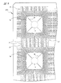
(実施の形態1)
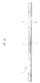
図1は、本実施の形態によるQFNの外観(表面側)を示す平面図、図2は、QFNの外観(裏面側)を示す平面図、図3は、QFNの内部構造(表面側)を示す平面図、図4は、QFNの内部構造(裏面側)を示す平面図、図5および図6は、QFNの断面図である。
【0014】
本実施の形態のQFN1は、1個の半導体チップ2を合成樹脂からなる封止体3によって封止した表面実装型のパッケージ構造を有しており、封止体3の外形寸法は、例えば縦×横=12mm×12mm、高さ=0.9mmである。
【0015】
半導体チップ2は、金属製のダイパッド部4上に搭載された状態で封止体3の中央部に配置されている。半導体チップ2の外形寸法は、例えば縦×横=4mm×4mm、厚さ=0.28mmである。また、ダイパッド部4は、例えば一辺のサイズが4mm〜7mmの範囲内にある異種の半導体チップ2を搭載可能とするために、その径を半導体チップ2の径よりも小さくした、いわゆる小タブ構造を有しており、本実施の形態では、例えば3mmの径を有している。
【0016】
半導体チップ2を搭載するダイパッド部4は、4本の吊りリード5bによって支持されている。これらの吊りリード5bの一端部側(半導体チップ2に近い側)は、ダイパッド部4に接続されており、他端部側は、封止体3のコーナー部に延在している。封止体3のコーナー部における吊りリード5bの幅は、他の部分の幅よりも広くなっている。
【0017】
ダイパッド部4の周囲には、複数本(例えば116本)のリード5がダイパッド部4を囲むように配置されている。これらのリード5の一端部側(半導体チップ2に近い側)5aは、Auワイヤ6を介して半導体チップ2の主面のボンディングパッド7に電気的に接続されている。また、これらのリード5の他端部側5cは、封止体3の側面で終端している。これらのリード5とダイパッド部4および吊りリード5bのそれぞれの厚さは、75μm程度である。
【0018】
図3に示すように、上記リード5のそれぞれは、半導体チップ2との距離を短くするために、一端部側5aが半導体チップ2の近傍まで引き回され、その先端のピッチ(P3)は他端部側5cのピッチよりも狭くなっている(例えば0.18mm〜0.2mm)。このように、リード5の一端部側5aをダイパッド部4の近傍まで引き回すことにより、リード5とボンディングパッド7を結線するAuワイヤ6の長さを短く(例えば3mm以下)することができる。これにより、QFN1を多ピン化した場合でも、またQFN1の多ピン化に伴ってリード5のピッチ、すなわちAuワイヤ6の間隔が狭くなった場合でも、QFN1の製造工程(例えばワイヤボンディング工程や樹脂モールド工程)でAuワイヤ6同士が接触する短絡不良の発生を抑制することができる。
【0019】
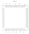
図2に示すように、QFN1の裏面(基板実装面)には、複数個(例えば116個)の外部接続端子5dが設けられている。これらの端子5dは、封止体3の各辺に沿って千鳥状に2列ずつ配置され、それぞれの端子5dの先端部分は、封止体3の裏面から露出し、かつ外側に突出している。また、これらの端子5dは、実装面積を確保するために、それらの幅がリード5の幅よりも広くなっている。端子5dの径(d)は、0.3mmであり、隣接する端子5dとのピッチは、同一列の端子5dとのピッチ(P1)が0.65mm、他の列の端子とのピッチ(P2)が0.325mmである。
【0020】
上記端子5dは、リード5と一体に形成されており、端子5dが形成された部分のリード5の厚さは、150μm程度である。封止体3の外側に突出した端子5dの先端部分には、メッキ法あるいは印刷法によって半田層9が被着されており、この半田層9を含む端子5dの高さ、すなわち封止体3の裏面から外側に突出する量(スタンドオフ量)が少なくとも50μm以上となるように、半田層9の膜厚が規定されている。本実施形態のQFN1は、これらの端子5dを配線基板の電極(フットプリント)に半田付けすることによって実装される。
【0021】
図1および図6に示すように、上記封止体3の表面側の対角線方向に沿った2つのコーナー部には、前記吊りリード5bの他端部側を露出させるための切り欠き部8が設けられている。これらの切り欠き部8から露出した吊りリード5bの一部には、例えば円形の平面形状を有する認識マーク15が設けられており、QFN1を配線基板に実装する際などに、封止体3の表面側から認識マーク15を光学的に認識できるようになっている。認識マーク15は、吊りリード5bを構成する金属板の一部をエッチングで除去、またはプレスで打ち抜くことによって形成される。
【0022】
図7は、本実施の形態のQFN1の製造に使用するリードフレームLF1の全体平面図、図8は、図7の一部(QFN約2個分の領域)を示す拡大平面図である。
【0023】
このリードフレームLF1は、Cu、Cu合金またはFe−Ni合金などの金属板からなり、前述したダイパッド部4、リード5、吊りリード5bなどのパターンが縦および横方向に繰り返し形成された構成になっている。すなわち、リードフレームLF1は、複数個(例えば24個)の半導体チップ2を搭載する多連構造になっている。
【0024】
上記リードフレームLF1を製造するには、図9に示すような板厚150μm程度のCu、Cu合金またはFe−Ni合金などからなる金属板10を用意し、ダイパッド部4、リード5および吊りリード5bを形成する箇所の片面をフォトレジスト膜11で被覆する。また、外部接続用の端子5dを形成する箇所は、両面をフォトレジスト膜11で被覆する。そして、この状態で金属板10を薬液によってエッチングし、片面がフォトレジスト膜11で被覆された領域の金属板10の板厚を半分程度(75μm程度)まで薄くする(ハーフエッチング)。このような方法でエッチングを行うことにより、両面共にフォトレジスト膜11で被覆されていない領域の金属板10は完全に消失し、片面がフォトレジスト膜11で被覆された領域に厚さ75μm程度のダイパッド部4、リード5および吊りリード5bが形成される。また、両面がフォトレジスト膜11で被覆された領域の金属板10は薬液によってエッチングされないので、エッチング前と同じ厚さ(150μm程度)を有する突起状の端子5dが形成される。次に、フォトレジスト膜11を除去し、続いて図9には示さない吊りリード5bの他端部側をプレスで打ち抜いて前述した認識マーク15を形成した後、リード5の一端部側5aの表面にAgメッキを施すことによって、リードフレームLF1が完成する。なお、認識マーク15は、上記フォトレジスト膜11をマスクに用いたエッチングでダイパッド部4、リード5、吊りリード5bおよび端子5dを形成する際に同時に形成することもできる。
【0025】
認識マーク15の形状は、例えば図10に示す四角形、図11に示す十字形など、封止体3の表面側から光学的に認識できる形状であれば任意の形状でよい。また、図12に示すように、2つのコーナー部に設ける認識マーク15を互いに異なる形状で構成してもよい。このようにすると、配線基板の実装面に水平な面内でQFN1が180度ずれた場合でも、そのずれを容易に検出することができる。
【0026】
上記リードフレームLF1を使ってQFN1を製造するには、まず図13に示すように、半導体チップ2の素子形成面を上に向けてダイパッド部4上に搭載し、Auペーストやエポキシ樹脂系接着剤を使って両者を接着する。
【0027】
次に、図14に示すように、周知のボールボンディング装置を使って半導体チップ2のボンディングパッド7とリード5の一端部側5aとの間をAuワイヤ6で結線する。図15に示すように、Auワイヤ6のボンディング時、あるいは前記半導体チップ2とダイパッド部4の接着時には、リードフレームLF1を支持する治具30Bの端子5dと対応する箇所に溝31を形成したり、ダイパッド部4と対応する箇所に突起32を形成したりしておくことにより、リードフレームLF1を安定して支持することができるので、Auワイヤ6とリード5の位置ずれや、半導体チップ2とダイパッド部4の位置ずれを防ぐことができる。
【0028】
次に、上記リードフレームLF1を図16に示すモールド金型40に装着して半導体チップ2を樹脂封止する。図16は、モールド金型40の一部(QFN約1個分の領域)を示す断面図である。
【0029】
モールド金型40を使って半導体チップ2を樹脂封止する際には、まず下型40Bの表面に薄い樹脂シート41を敷き、この樹脂シート41の上にリードフレームLF1を載置する。リードフレームLF1は、突起状の端子5dが形成された面を下に向けて載置し、端子5dと樹脂シート41とを接触させる。そしてこの状態で、樹脂シート41とリードフレームLF1を上型40Aと下型40Bで挟み付ける。このようにすると、図に示すように、リード5の下面に位置する端子5dが金型40(上型40Aおよび下型40B)の押圧力によって樹脂シート41を押さえ付けるので、その先端部分が樹脂シート41の中に食い込む。
【0030】
この結果、図17に示すように、上型40Aと下型40Bの隙間(キャビティ)に溶融樹脂を注入して封止体3を成形した後、上型40Aと下型40Bを分離すると、樹脂シート41の中に食い込んでいた端子5dの先端部分が封止体3の裏面から外側に突出する。このとき、図18に示すように、封止体3の表面側の2つのコーナー部には切り欠き部8が形成され、認識マーク15が形成された吊りリード5bの端部が露出する。
【0031】
図19は、上記金型40の上型40AがリードフレームLF1と接触する部分を斜線で示した平面図である。また、図20は、この金型40のゲートの位置と、キャビティに注入された樹脂の流れる方向を模式的に示した平面図である。
【0032】
図19に示すように、上記金型40は、リードフレームLF1の外枠部分、およびリード5とリード5の連結部分のみが上型40Aと接触し、それ以外の全ての領域は、樹脂が注入されるキャビティとして有効に利用される構造になっている。
【0033】
また、図20に示すように、上記金型40の一辺には複数のゲートG1〜G16が設けられており、例えば図の左端の縦方向に並んだ3つのキャビティC1〜C3には、ゲートG1、G2を通じて樹脂が注入され、これらに隣接する3つのキャビティC4〜C6には、ゲートG3、G4を通じて樹脂が注入される構造になっている。一方、上記ゲートG1〜G16と対向する他の一辺には、ダミーキャビティDC1〜DC8およびエアベント42が設けられており、例えばゲートG1、G2を通じてキャビティC1〜C3に樹脂が注入されると、キャビティC1〜C3内のエアーがダミーキャビティDC1に流入し、キャビティC3内の樹脂にボイドが生じるのを防止する構造になっている。
【0034】
図21は、上記キャビティC1〜C18に樹脂を注入して封止体3を成形した後、金型40から取り外したリードフレームLF1の平面図、図22は、図21のX−X’線に沿った断面図、図23は、リードフレームLF1の裏面側の平面図である。
【0035】
その後、リードフレームLF1の裏面に露出した端子5dの表面に半田層(9)を形成し、続いて封止体3の表面に製品名などのマークを印刷した後、図21に示すダイシングラインLに沿ってリードフレームLF1およびモールド樹脂の一部を切断することにより、前記図1〜図6に示した本実施形態のQFN1が完成する。
【0036】
図24は、本実施の形態のQFN1をSOP(Small Outline Package)、QFP(Quad Flat Package)といった他の表面実装型パッケージと共に配線基板20に実装した状態を示す平面図である。SOPおよびQFPは、パッケージの側面からリード33が外側に露出しているので、これらリード33の位置を配線基板20の上方から光学的に認識することによって、リード33と配線基板20の位置合わせを正確に行うことができる。
【0037】
一方、QFN1の場合は、封止体3の2つのコーナー部に露出した認識マーク15の位置を配線基板20の上方から光学的に認識することによって、端子5dと配線基板20との位置合わせを行う。前述したように、認識マーク15は、ダイパッド部4、リード5、吊りリード5bおよび端子5dと同時に形成されるため、認識マーク15と端子5dとの間には相対的な位置ずれがない。従って、認識マーク15の位置を配線基板20の上方から光学的に認識することによって、配線基板20の上方からは認識できない端子5dと配線基板20の位置合わせを正確に行うことができる。
【0038】
本実施の形態のQFN1は、ダイパッド部4、リード5、吊りリード5bおよび端子5dを形成する工程で認識マーク15を同時に形成するので、認識マーク15を形成するための特別な工程は不要である。
【0039】
また、本実施の形態のQFN1は、リード5の一端部側5aをダイパッド部4の近傍まで引き回しているので、一端部側5aと半導体チップ2との間の距離を短くすることができ、それら接続するAuワイヤ6の長さも短くすることができる。また、端子5dを千鳥状に配置してもリード5の一端部側5aの長さはほぼ等しいので、一端部側5aの先端が半導体チップ2の各辺に対してほぼ一列に並ぶ。従って、リード5の一端部側5aと半導体チップ2とを接続するAuワイヤ6の長さをほぼ均等にすることができると共に、Auワイヤ6のループ形状もほぼ均等にすることができる。
【0040】
これにより、隣接するAuワイヤ6同士が短絡したり、特に半導体チップ2の四隅近傍でAuワイヤ6同士が交差したりする不具合が生じないので、ワイヤボンディングの作業性が向上する。また、隣接するAuワイヤ6間のピッチを狭くすることができるので、QFN1の多ピン化を実現することができる。
【0041】
また、リード5の一端部側5aをダイパッド部4の近傍まで引き回したことにより、端子5dからリード5の一端部側5aまでの距離が長くなる。これにより、封止体3の外部に露出した端子5dを通じて封止体3の内部に浸入する水分が半導体チップ2に到達し難くなるので、水分によるボンディングパッド7の腐食を防止することができ、QFN1の信頼性が向上する。
【0042】
また、リード5の一端部側5aをダイパッド部4の近傍まで引き回すことにより、半導体チップ2をシュリンクしてもAuワイヤ6の長さの増加は極めて僅か(例えば半導体チップ2を4mm角から3mm角にシュリンクしても、Auワイヤ6の長さの増加は、平均0.7mm程度)であるため、半導体チップ2のシュリンクに伴うワイヤボンディングの作業性の低下を防止することができる。
【0043】
(実施の形態2)
前記実施の形態1では、小タブ構造のリードフレームLF1を使って製造したQFNについて説明したが、例えば図25および図26に示すように、リード5の一端部側5aに絶縁フィルムからなるチップ支持体34を貼り付けたリードフレームLF2を使用して製造することも可能である。
【0044】
また、前記実施の形態1のリードフレームLF1は、ダイパッド部4を4本の吊りリード5bで支持しているが、本実施の形態のリードフレームLF2は、チップ支持体34をリード5の一端部側5aで支持する構造になっているので、吊りリード5bは存在しない。そこで、本実施の形態では、図25に示すように、半導体チップ2に電気的に接続されない位置合わせ用リード5eを設け、この位置合わせ用リード5eの一部に認識マーク15を形成する。
【0045】
本実施形態で使用するリードフレームLF2は、前記実施の形態1のリードフレームLF1に準じた方法で製造することができる。すなわち、図27に示すような板厚150μm程度の金属板10を用意し、リード5を形成する箇所の片面をフォトレジスト膜11で被覆する。また、外部接続用の端子5dを形成する箇所には、両面にフォトレジスト膜11を形成する。図示はしないが、位置合わせ用リード5eを形成する箇所は、片面にフォトレジスト膜11を形成し、認識マーク15を形成する箇所のみ、両面共フォトレジスト膜11を形成しない。
【0046】
そして、前記実施の形態1で説明した方法で金属板10をハーフエッチングすることによって、厚さ75μm程度のリード5および位置合わせ用リード5eと厚さ150μm程度の端子5dを同時に形成した後、リード5の一端部側5aの表面にAgメッキを施し、最後にこの一端部側5aの片面にチップ支持体34を接着する。なお、チップ支持体34は、絶縁フィルムに代えて、薄い金属板のような導電材料によって構成してもよい。この場合は、リード5同士のショートを防ぐために、絶縁性の接着剤を使ってリード5とチップ支持体34を接着すればよい。また、金属箔の表面に絶縁性の樹脂を塗布したシートなどによってチップ支持体34を構成することもできる。
【0047】
上記のようなリードフレームLF2を使用する場合も、金属板10の一部の片面をフォトレジスト膜11でマスクしてハーフエッチングを施すことにより、リード5の板厚を金属板10の半分程度まで薄くすることができるので、リード5の一端部側5aのピッチが極めて狭い(例えば0.18mm〜0.2mmピッチ)リード5を精度よく加工することができる。また、金属板10の一部の両面をフォトレジスト膜11でマスクすることにより、突起状の端子5dをリード5と同時に形成することができる。
【0048】
上記リードフレームLF2は、チップ支持体34をリード5で支持するので、リード5の一端部側5aと半導体チップ2の距離が短くなり、Auワイヤ6の長さをさらに短くすることができる。さらに、ダイパッド部4を4本の吊りリード5bで支持する場合に比べてチップ支持体34を確実に支持できるので、モールド工程で金型内に溶融樹脂を注入した際、チップ支持体34の変位が抑制され、Auワイヤ6同士の短絡不良が防止できる。
【0049】
図28に示すように、このリードフレームLF2を使ったQFN1の製造方法は、前記実施の形態1で説明した方法と概略同一である。
【0050】
図29は、樹脂モールド工程が完了したリードフレームLF2の一部を示す平面図である。図に示すように、封止体3の表面側の対角線方向に沿った2つのコーナー部近傍には切り欠き部8が設けられ、前記認識マーク15が形成された位置合わせ用リード5eが露出している。従って、本実施の形態のQFN1においても、この認識マーク15の位置を上方から光学的に認識することによって、封止体3の表面側から見えない端子5dと配線基板の位置合わせを正確に行うことができる。
【0051】
(実施の形態3)
図30は、本実施の形態のQFNの外観(表面側)を示す平面図、図31は、QFNの外観(裏面側)を示す平面図、図32は、QFNの内部構造(表面側)を示す平面図、図33は、QFNの内部構造(裏面側)を示す平面図、図34〜図36は、QFNの断面図である。
【0052】
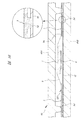
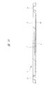
本実施の形態のQFN1は、1個の半導体チップ2を合成樹脂からなる封止体3によって封止した構造を有しており、封止体3の外形寸法は、例えば縦×横=12mm×12mm、高さ=0.5mmである。ダイパッド部4上に搭載された状態で封止体3の中央部に配置された半導体チップ2の外形寸法は、例えば縦×横=4mm×4mm、厚さは0.14mmである。ダイパッド部4は、小タブ構造を有しており、4本の吊りリード5bによって支持されている。ダイパッド部4の周囲に配置されたリード5の一端部側(半導体チップ2に近い側)5aは、Auワイヤ6を介して半導体チップ2の主面のボンディングパッド7に電気的に接続されており、他端部側5cは、封止体3の側面で終端している。リード5のそれぞれは、半導体チップ2との距離を短くするために、一端部側5aがダイパッド部4の近傍まで引き回され、その先端のピッチは他端部側5cよりも狭いピッチとなっている。
【0053】
図30に示すように、封止体3の表面の対角線方向に沿った2つのコーナー部近傍には、2本の吊りリード5bの各一部が露出している。吊りリード5bは、封止体3の表面に露出した部分が封止体3の内部にある部分に比べて幅が広くなっている。封止体3の表面に露出した吊りリード5bの一部には、認識マーク15が設けられており、QFN1を配線基板に実装する際などに、封止体3の表面側から認識マーク15を光学的に認識できるようになっている。
【0054】
図35に示すように、上記2本の吊りリード5bは、封止体3の表面に露出した部分、すなわち認識マーク15が設けられた部分が封止体3の表面と同じ高さとなるように上方に折り曲げられている。一方、図36に示すように、認識マーク15が設けられていない残り2本の吊りリード5bは、上方に折り曲げられていない。
【0055】
図31および図34に示すように、封止体3の裏面には、前記複数本のリード5のそれぞれの一部を下方に折り曲げて形成した複数個(例えば116個)の外部接続端子5dが、封止体3の各辺に沿って千鳥状に2列ずつ配置されている。これらの端子5dは、封止体3の裏面から外側に突出しており、その表面には、印刷法またはメッキ法によって半田層9が形成されている。半田層9を含む端子5dの高さ、すなわち封止体3の裏面からの突出量(スタンドオフ量)は、少なくとも50μm以上となるように、リード5の折り曲げ量および半田層9の膜厚が規定されている。それぞれの端子5dの幅は、配線基板との実装面積を確保するために、リード5の幅よりも広くなっている。
【0056】
図37は、本実施の形態のQFN1の製造に用いるリードフレームLF3の平面図である。このリードフレームLF3は、Cu、Cu合金またはFe−Ni合金からなる板厚100μm〜150μm程度の金属板からなり、前述したダイパッド部4、リード5、吊りリード5bなどのパターンが縦および横方向に繰り返し形成された多連構造を有し、例えば24個の半導体チップ2を搭載することができるようになっている。
【0057】
上記リードフレームLF3を製造するには、図38に示すように、まず金属板10をプレスで打ち抜いてリード5、吊りリード5b、ダイパッド部4、認識マーク15などのパターンを形成し、続いてリード5の中途部をプレスで下方に折り曲げることによって端子5dを形成する。またこのとき、図39に示すように、吊りリード5bの中途部(認識マーク15が形成された部分)をプレスで上方に折り曲げる。
【0058】
端子5dを形成するには、図40に示すように、金属板10をプレス金型50の上型50Aと下型50Bの間に挟み込む。そして、この状態で上型50Aに設けたパンチ51を下型50Bに設けたダイ52に押し込むと、各リード5の中途部が塑性変形して下方に折れ曲がり、端子5dが形成される。図示は省略するが、吊りリード5bを上方に折り曲げるには、下型50Bに設けたパンチ51を上型50Aに設けたダイ52に押し込めばよい。その後、リード5の一端部側5aの一面(Auワイヤ6をボンディングする領域)に電解メッキ法でAgメッキ層を形成することにより、リードフレームLF3が完成する。
【0059】
このように、本実施の形態では、金属板10をプレスで剪断加工することによって、リード5、吊りリード5b、ダイパッド部4、端子5d、認識マーク15などのパターンを形成するので、これらのパターンをエッチングで形成する場合に比べてリードフレームLF3の製造工程が簡略化され、その製造コストを低減することが可能となる。
【0060】
上記リードフレームLF3のダイパッド部4に半導体チップ2を搭載し、続いて半導体チップ2のボンディングパッド7とリード5の一端部側5aとの間をAuワイヤ6で結線した後、リードフレームLF3をモールド金型に装着して半導体チップ2を封止する方法は、前記実施の形態1と同じである。
【0061】
図41は、モールド金型から取り外したリードフレームLF3の表面側を示す要部平面図、図42は、リードフレームLF3の裏面側を示す要部平面図である。図に示すように、リードフレームLF3をモールド金型から取り外すと、封止体3の表面には2本の吊りリード5bの各一部(認識マーク15が形成された部分)が露出し、封止体3の裏面には複数の端子5dが露出する。
【0062】
次に、図43に示すように、封止体3の裏面から露出した端子5dの表面に半田層9を形成する。半田層9を形成するには、電解メッキ法または印刷法を用いるが、短時間で厚い半田層9を形成できる半田印刷法が好ましい。半田印刷法を用いる場合は、メタルマスクを用いたスクリーン印刷法で膜厚30μm〜100μm程度の半田を印刷し、次いで加熱炉内でリードフレームLF3を加熱することによって半田をリフローする。
【0063】
図示は省略するが、その後、封止体3の表面に製品名などのマークを印刷し、続いて封止体3の外部に露出したリード5の連結部をダイシングまたはダイパンチによって切断して封止体3を個片化することにより、前記図30〜図36に示した本実施の形態のQFN1が完成する。
【0064】
本実施の形態のQFN1は、封止体3の裏面から外側に突出した上記複数個の端子5dを配線基板の電極(フットプリント)に半田付けすることによって実装される。その際、封止体3の2つのコーナー部に露出した認識マーク15の位置を配線基板の上方から光学的に認識することによって、端子5dと配線基板との位置合わせを行う。認識マーク15は、ダイパッド部4、リード5、吊りリード5bおよび端子5dと同時に形成されるため、認識マーク15と端子5dとの間には相対的な位置ずれがない。従って、認識マーク15の位置を配線基板の上方から光学的に認識することによって、配線基板20の上方からは認識できない端子5dと配線基板20の位置合わせを正確に行うことができる。
【0065】
また、本実施の形態によれば、リード5、吊りリード5b、ダイパッド部4、端子5d、認識マーク15などのパターンをプレスで形成するので、これらのパターンをエッチングで形成する場合に比べてリードフレームLF3の製造工程が簡略化される。これにより、リードフレームLF3の製造コストを低減することができるので、このリードフレームLF3を使ったQFN1の製造コストを低減することができる。
【0066】
端子5dの平面形状は、四角形、楕円形など、種々の形状を採用することができる。さらに、端子数が比較的少ないQFNの場合には、多ピンのQFNに比べてリード5の幅が広いため、端子5dの幅をリード5の幅と同じにしてもよい。
【0067】
以上、本発明者によってなされた発明を発明の実施の形態に基づき具体的に説明したが、本発明は前記発明の実施の形態に限定されるものではなく、その要旨を逸脱しない範囲で種々変更可能であることは言うまでもない。
【0068】
【発明の効果】
本願において開示される発明のうち、代表的なものによって得られる効果を簡単に説明すれば以下のとおりである。
【0069】
QFNを構成する封止体の上面にリードの一部を露出させ、そこに認識マークを形成することにより、QFNを配線基板に実装する際、認識まマークの位置を配線基板の上方から光学的に認識することによって、封止体の裏面に配置された外部接続端子と配線基板との位置合わせを高精度に行うことができる。
【図面の簡単な説明】
【図1】本発明の一実施の形態である半導体装置の外観(表面側)を示す平面図である。
【図2】本発明の一実施の形態である半導体装置の外観(裏面側)を示す平面図である。
【図3】本発明の一実施の形態である半導体装置の内部構造(表面側)を示す平面図である。
【図4】本発明の一実施の形態である半導体装置の内部構造(裏面側)を示す平面図である。
【図5】本発明の一実施の形態である半導体装置の断面図である。
【図6】本発明の一実施の形態である半導体装置の断面図である。
【図7】本発明の一実施の形態である半導体装置の製造に用いるリードフレームの全体平面図である。
【図8】図7に示すリードフレームの一部を示す拡大平面図である。
【図9】図7に示すリードフレームの製造方法を示す断面図である。
【図10】吊りリードの一部に形成された認識マークの形状の一例を示すリードフレームの要部平面図である。
【図11】吊りリードの一部に形成された認識マークの形状の一例を示すリードフレームの要部平面図である。
【図12】吊りリードの一部に形成された認識マークの形状の一例を示すリードフレームの要部平面図である。
【図13】本発明の一実施の形態である半導体装置の製造方法を示す半導体チップ接着後のリードフレームの要部平面図である。
【図14】本発明の一実施の形態である半導体装置の製造方法を示すワイヤボンディング後のリードフレームの要部平面図である。
【図15】本発明の一実施の形態である半導体装置の製造方法を示す概略断面図である。
【図16】本発明の一実施の形態である半導体装置の製造方法を示すモールド金型およびリードフレームの要部断面図である。
【図17】本発明の一実施の形態である半導体装置の製造方法を示すモールド金型およびリードフレームの要部断面図である。
【図18】本発明の一実施の形態である半導体装置の製造方法を示すモールド金型およびリードフレームの要部断面図である。
【図19】本発明の一実施の形態である半導体装置の製造方法を示すモールド金型(上型)とリードフレームとの接触部分を示す平面図である。
【図20】本発明の一実施の形態である半導体装置の製造方法を示すモールド金型のゲート位置とキャビティに注入される樹脂の流れる方向を模式的に示す平面図である。
【図21】本発明の一実施の形態である半導体装置の製造方法を示すモールド後のリードフレームの平面図である。
【図22】図21のX−X’線に沿ったリードフレームの断面図である。
【図23】本発明の一実施の形態である半導体装置の製造方法を示すモールド後のリードフレームの平面図である。
【図24】本発明の一実施の形態である半導体装置を他の表面実装型半導体装置と共に配線基板に実装した状態を示す平面図である。
【図25】本発明の他の実施の形態である半導体装置の製造に用いるリードフレームの要部平面図である。
【図26】本発明の他の実施の形態である半導体装置の製造に用いるリードフレームの要部断面図である。
【図27】図25に示すリードフレームの製造方法を示す断面図である。
【図28】本発明の他の実施の形態である半導体装置の製造方法を示すリードフレームの要部断面図である。
【図29】本発明の他の実施の形態である半導体装置の製造方法を示すモールド後のリードフレームの要部平面図である。
【図30】本発明の他の実施の形態である半導体装置の外観(表面側)を示す平面図である。
【図31】本発明の他の実施の形態である半導体装置の外観(裏面側)を示す平面図である。
【図32】本発明の他の実施の形態である半導体装置の内部構造(表面側)を示す平面図である。
【図33】本発明の他の実施の形態である半導体装置の内部構造(裏面側)を示す平面図である。
【図34】本発明の他の実施の形態である半導体装置の断面図である。
【図35】本発明の他の実施の形態である半導体装置の断面図である。
【図36】本発明の他の実施の形態である半導体装置の断面図である。
【図37】本発明の他の実施の形態である半導体装置の製造に用いるリードフレームの全体平面図である。
【図38】図37に示すリードフレームの製造方法を示す断面図である。
【図39】図37に示すリードフレームの製造方法を示す断面図である。
【図40】本発明の他の実施の形態である半導体装置の製造方法を示すプレス金型およびリードフレームの要部断面図である。
【図41】本発明の他の実施の形態である半導体装置の製造方法を示すモールド後のリードフレームの要部平面図である。
【図42】本発明の他の実施の形態である半導体装置の製造方法を示すモールド後のリードフレームの要部平面図である。
【図43】本発明の他の実施の形態である半導体装置の製造方法を示すモールド後のリードフレームの要部断面図である。
【符号の説明】
1 QFN
2 半導体チップ
3 封止体
4 ダイパッド部
5 リード
5a リードの一端部側
5b 吊りリード
5c リードの他端部側
5d 外部接続端子
5e 位置合わせ用リード
6 Auワイヤ
7 ボンディングパッド
8 切り欠き部
9 半田層
10 金属板
11 フォトレジスト膜
15 認識マーク
20 配線基板
30B 治具
31 溝
32 突起
33 リード
34 チップ支持体
40 モールド金型
40A 上型
40B 下型
41 樹脂シート
42 エアベント
50 プレス金型
50A 上型
50B 下型
51 パンチ
52 ダイ
53 突起
d 端子の径
G1〜G16 ゲート
C1〜C24 キャビティ
DC1〜DC8 ダミーキャビティ
LF1〜LF3 リードフレーム
P1 端子間ピッチ(同一列)
P2 端子間ピッチ(異なる列)
P3 リード一端部側先端ピッチ[0001]
BACKGROUND OF THE INVENTION
The present invention relates to a semiconductor device and a manufacturing technique thereof, and more particularly to a technology for mounting a resin-encapsulated semiconductor device having an external connection terminal on a back surface of a package on a wiring board with high accuracy.
[0002]
[Prior art]
There is a QFN (Quad Flat Non-leaded package) as a kind of a resin package in which a semiconductor chip mounted on a lead frame is sealed with a sealing body made of a mold resin.
[0003]
The QFN constitutes an external connection terminal by exposing one end portion of each of a plurality of leads electrically connected to the semiconductor chip via a bonding wire from the back surface (lower surface) of the outer peripheral portion of the sealing body. A bonding wire is connected to a surface opposite to the exposed surface, that is, a terminal surface inside the sealing body to electrically connect the terminal and the semiconductor chip. These terminals are mounted by soldering to the electrodes (footprints) of the wiring board. This structure has an advantage that the mounting area is reduced as compared with a QFP (Quad Flat Package) in which the leads extend in the lateral direction from the side surface of the package (sealing body) to form the terminals.
[0004]
The QFN is described in, for example, Japanese Patent Application Laid-Open No. 2001-189410 and Japanese Patent No. 3072291.
[0005]
[Problems to be solved by the invention]
The QFP in which the lead extends laterally from the side surface of the sealing body to constitute the external connection terminal can optically detect the position of the external connection terminal from above when mounted on the wiring board. And external connection terminals can be easily aligned.
[0006]
On the other hand, the QFN in which the external connection terminal is disposed on the back surface (lower surface) of the sealing body cannot optically detect the position of the external connection terminal from above. For this reason, when positioning the wiring board and the external connection terminal, an expensive positioning device having a complicated optical system for optically detecting the position of the external connection terminal from an obliquely lower side is required, and the mounting cost of the QFN is required. Has been rising.
[0007]
An object of the present invention is to provide a technique capable of improving the mounting accuracy of a QFN without using an expensive positioning device having a complicated optical system.
[0008]
The above and other objects and novel features of the present invention will be apparent from the description of this specification and the accompanying drawings.
[0009]
[Means for Solving the Problems]
Of the inventions disclosed in the present application, the outline of typical ones will be briefly described as follows.
[0010]
The semiconductor device of the present invention includes a semiconductor chip, a die pad portion on which the semiconductor chip is mounted, a suspension lead that supports the die pad portion, a plurality of leads disposed around the die pad portion, and the semiconductor chip. A plurality of wires that electrically connect the leads; and a sealing body that seals the semiconductor chip, the die pad portion, the suspension leads, the plurality of leads, and the plurality of wires.
Each of the plurality of leads is selectively provided with an external connection terminal protruding outside from the back surface of the sealing body, and a part of the suspension lead is exposed to the outside from the top surface of the sealing body. A recognition mark for aligning the external connection terminal with the wiring board is formed on the suspension lead in a region exposed to the outside from the upper surface of the sealing body.
[0011]
Accordingly, when the semiconductor device is mounted on the wiring board, the position of the recognition mark is optically detected from above, so that the external connection terminals arranged on the back side of the sealing body are accurately positioned on the wiring board. be able to.
[0012]
DETAILED DESCRIPTION OF THE INVENTION
Hereinafter, embodiments of the present invention will be described in detail with reference to the drawings. Note that components having the same function are denoted by the same reference symbols throughout the drawings for describing the embodiments, and the repetitive description thereof will be omitted. In the following embodiments, the description of the same or similar parts will not be repeated in principle unless particularly necessary.
[0013]
(Embodiment 1)
1 is a plan view showing the appearance (front side) of the QFN according to the present embodiment, FIG. 2 is a plan view showing the appearance (back side) of the QFN, and FIG. 3 shows the internal structure (front side) of the QFN. FIG. 4 is a plan view showing the internal structure (back side) of the QFN, and FIGS. 5 and 6 are cross-sectional views of the QFN.
[0014]
The
[0015]
The
[0016]
The
[0017]
Around the
[0018]
As shown in FIG. 3, in order to shorten the distance from the
[0019]
As shown in FIG. 2, a plurality (for example, 116) of
[0020]
The terminal 5d is formed integrally with the
[0021]
As shown in FIGS. 1 and 6, at two corner portions along the diagonal direction on the surface side of the sealing
[0022]
FIG. 7 shows a lead frame LF used for manufacturing the
[0023]
This lead frame LF 1 Is made of a metal plate such as Cu, Cu alloy or Fe—Ni alloy, and has a configuration in which the patterns such as the
[0024]
[0025]
The shape of the
[0026]
Lead frame LF 1 First, as shown in FIG. 13, the
[0027]
Next, as shown in FIG. 14, the
[0028]
Next, the lead frame LF 1 Is mounted on a
[0029]
When resin-sealing the
[0030]
As a result, as shown in FIG. 17, after the molten resin is injected into the gap (cavity) between the
[0031]
FIG. 19 shows that the
[0032]
As shown in FIG. 19, the
[0033]
Further, as shown in FIG. 20, a plurality of gates G are provided on one side of the
[0034]
FIG. 21 shows the cavity C 1 ~ C 18 The lead frame LF removed from the
[0035]
After that, lead frame LF 1 After a solder layer (9) is formed on the surface of the terminal 5d exposed on the back surface of the substrate, a mark such as a product name is printed on the surface of the sealing
[0036]
FIG. 24 is a plan view showing a state in which the
[0037]
On the other hand, in the case of
[0038]
In the
[0039]
In addition, since the
[0040]
As a result, there is no inconvenience that
[0041]
Further, since the one
[0042]
Further, by extending the one
[0043]
(Embodiment 2)
In the first embodiment, the lead frame LF having a small tab structure 1 The QFN manufactured by using the lead frame LF has been described. For example, as shown in FIGS. 25 and 26, a lead frame LF in which a
[0044]
The lead frame LF of the first embodiment 1 The
[0045]
Lead frame LF used in this embodiment 2 Is the lead frame LF of the first embodiment 1 It can manufacture by the method according to. That is, a
[0046]
Then, by half-etching the
[0047]
Lead frame LF as above 2 Can be reduced to about half the thickness of the
[0048]
Lead frame LF 2 Since the
[0049]
As shown in FIG. 28, this lead frame LF 2 The manufacturing method of QFN1 using is substantially the same as the method described in the first embodiment.
[0050]
FIG. 29 shows the lead frame LF after the resin molding process is completed. 2 It is a top view which shows a part of. As shown in the figure,
[0051]
(Embodiment 3)
30 is a plan view showing the appearance (front side) of the QFN of the present embodiment, FIG. 31 is a plan view showing the appearance (back side) of the QFN, and FIG. 32 shows the internal structure (front side) of the QFN. FIG. 33 is a plan view showing the internal structure (back side) of the QFN, and FIGS. 34 to 36 are cross-sectional views of the QFN.
[0052]
The
[0053]
As shown in FIG. 30, a part of each of the two suspension leads 5 b is exposed in the vicinity of two corner portions along the diagonal direction of the surface of the sealing
[0054]
As shown in FIG. 35, the two suspension leads 5b are arranged such that the portion exposed on the surface of the sealing
[0055]
As shown in FIGS. 31 and 34, a plurality of (for example, 116)
[0056]
FIG. 37 shows a lead frame LF used for manufacturing the
[0057]
Lead frame LF Three 38, first, the
[0058]
In order to form the terminal 5d, the
[0059]
As described above, in this embodiment, the
[0060]
Lead frame LF Three After the
[0061]
FIG. 41 shows the lead frame LF removed from the mold. Three FIG. 42 is a plan view of the main part showing the surface side of the lead frame LF. Three It is a principal part top view which shows the back surface side. As shown in the figure, the lead frame LF Three Is removed from the mold, each part of the two suspension leads 5b (the part where the
[0062]
Next, as shown in FIG. 43, a
[0063]
Although illustration is omitted, after that, a mark such as a product name is printed on the surface of the sealing
[0064]
The
[0065]
In addition, according to the present embodiment, patterns such as the
[0066]
Various shapes such as a quadrangle and an ellipse can be adopted as the planar shape of the terminal 5d. Further, in the case of the QFN having a relatively small number of terminals, the width of the
[0067]
Although the invention made by the present inventor has been specifically described based on the embodiments of the invention, the present invention is not limited to the embodiments of the invention, and various modifications can be made without departing from the scope of the invention. It goes without saying that it is possible.
[0068]
【The invention's effect】
Among the inventions disclosed in the present application, effects obtained by typical ones will be briefly described as follows.
[0069]
By exposing a part of the lead on the upper surface of the sealing body constituting the QFN and forming a recognition mark there, when the QFN is mounted on the wiring board, the position of the recognition mark is optically viewed from above the wiring board. By recognizing the above, the alignment between the external connection terminal disposed on the back surface of the sealing body and the wiring board can be performed with high accuracy.
[Brief description of the drawings]
FIG. 1 is a plan view showing an appearance (front side) of a semiconductor device according to an embodiment of the present invention;
FIG. 2 is a plan view showing the appearance (back side) of a semiconductor device according to an embodiment of the present invention;
FIG. 3 is a plan view showing an internal structure (surface side) of a semiconductor device according to an embodiment of the present invention;
FIG. 4 is a plan view showing an internal structure (back side) of a semiconductor device according to an embodiment of the present invention;
FIG. 5 is a cross-sectional view of a semiconductor device according to an embodiment of the present invention.
FIG. 6 is a cross-sectional view of a semiconductor device according to an embodiment of the present invention.
FIG. 7 is an overall plan view of a lead frame used for manufacturing a semiconductor device according to an embodiment of the present invention;
8 is an enlarged plan view showing a part of the lead frame shown in FIG. 7; FIG.
9 is a cross-sectional view showing a manufacturing method of the lead frame shown in FIG. 7; FIG.
FIG. 10 is a plan view of a principal part of a lead frame showing an example of a shape of a recognition mark formed on a part of a suspension lead.
FIG. 11 is a plan view of a principal part of a lead frame showing an example of a shape of a recognition mark formed on a part of a suspension lead.
FIG. 12 is a plan view of a main part of a lead frame showing an example of a shape of a recognition mark formed on a part of a suspension lead.
FIG. 13 is a plan view of relevant parts of a lead frame after semiconductor chip bonding, showing a method for manufacturing a semiconductor device according to an embodiment of the present invention;
FIG. 14 is a plan view of relevant parts of a lead frame after wire bonding showing a method for manufacturing a semiconductor device according to an embodiment of the present invention;
FIG. 15 is a schematic cross sectional view showing the method for manufacturing the semiconductor device according to one embodiment of the present invention.
16 is a cross-sectional view of main parts of a mold and a lead frame showing a method for manufacturing a semiconductor device according to an embodiment of the present invention; FIG.
17 is a cross-sectional view of main parts of a mold and a lead frame showing a method for manufacturing a semiconductor device according to an embodiment of the present invention; FIG.
18 is a cross-sectional view of main parts of a mold and a lead frame showing a method for manufacturing a semiconductor device according to an embodiment of the present invention; FIG.
19 is a plan view showing a contact portion between a mold die (upper die) and a lead frame showing a method for manufacturing a semiconductor device according to an embodiment of the present invention; FIG.
FIG. 20 is a plan view schematically showing the gate position of the mold and the flow direction of the resin injected into the cavity in the method for manufacturing the semiconductor device according to one embodiment of the present invention.
FIG. 21 is a plan view of the lead frame after molding showing the manufacturing method of the semiconductor device according to the embodiment of the invention;
22 is a cross-sectional view of the lead frame taken along line XX ′ in FIG. 21. FIG.
FIG. 23 is a plan view of the lead frame after molding showing the manufacturing method of the semiconductor device according to the embodiment of the invention;
FIG. 24 is a plan view showing a state in which the semiconductor device according to one embodiment of the present invention is mounted on a wiring board together with another surface-mount type semiconductor device.
25 is a substantial part plan view of a lead frame used for manufacturing a semiconductor device in another embodiment of the invention; FIG.
FIG. 26 is a fragmentary cross-sectional view of a lead frame used for manufacturing a semiconductor device in another embodiment of the invention;
27 is a cross-sectional view showing a manufacturing method of the lead frame shown in FIG. 25; FIG.
FIG. 28 is a cross-sectional view of the principal part of the lead frame showing the method of manufacturing a semiconductor device according to another embodiment of the present invention.
29 is a substantial part plan view of a lead frame after molding showing a method for manufacturing a semiconductor device in another embodiment of the invention; FIG.
30 is a plan view showing the appearance (surface side) of a semiconductor device according to another embodiment of the present invention; FIG.
FIG. 31 is a plan view showing the appearance (back side) of a semiconductor device according to another embodiment of the present invention;
FIG. 32 is a plan view showing an internal structure (surface side) of a semiconductor device according to another embodiment of the present invention;
FIG. 33 is a plan view showing an internal structure (back side) of a semiconductor device according to another embodiment of the present invention;
FIG. 34 is a cross-sectional view of a semiconductor device in another embodiment of the invention.
FIG. 35 is a cross-sectional view of a semiconductor device in another embodiment of the invention.
36 is a sectional view of a semiconductor device in another embodiment of the invention; FIG.
FIG. 37 is an overall plan view of a lead frame used for manufacturing a semiconductor device in another embodiment of the invention;
38 is a cross-sectional view showing a manufacturing method of the lead frame shown in FIG. 37;
39 is a cross-sectional view showing a manufacturing method of the lead frame shown in FIG. 37;
FIG. 40 is a cross-sectional view of main parts of a press die and a lead frame showing a method for manufacturing a semiconductor device according to another embodiment of the present invention.
41 is a substantial part plan view of a lead frame after molding showing a method for manufacturing a semiconductor device in another embodiment of the invention; FIG.
42 is a substantial part plan view of a lead frame after molding showing a method for manufacturing a semiconductor device in another embodiment of the invention; FIG.
43 is a substantial part sectional view of a lead frame after molding, illustrating a method for manufacturing a semiconductor device in another embodiment of the invention; FIG.
[Explanation of symbols]
1 QFN
2 Semiconductor chip
3 Sealing body
4 Die pad section
5 Lead
5a One end side of the lead
5b Hanging lead
5c The other end of the lead
5d External connection terminal
5e Positioning lead
6 Au wire
7 Bonding pads
8 Notch
9 Solder layer
10 Metal plate
11 Photoresist film
15 Recognition mark
20 Wiring board
30B Jig
31 groove
32 Protrusions
33 Lead
34 Chip support
40 Mold
40A Upper mold
40B Lower mold
41 resin sheet
42 Air Vent
50 press mold
50A Upper mold
50B Lower mold
51 punch
52 die
53 Protrusions
d Terminal diameter
G 1 ~ G 16 Gate
C 1 ~ C twenty four cavity
DC 1 ~ DC 8 Dummy cavity
LF 1 ~ LF Three Lead frame
P 1 Terminal pitch (same row)
P 2 Terminal pitch (different rows)
P Three Lead one end side tip pitch
Claims (3)
前記複数のリードのそれぞれには、前記封止体の裏面から外部に突出する外部接続端子が選択的に設けられ、
前記吊りリードの一部は、前記吊りリードの一部を上方に折り曲げることによって前記封止体の上面から外部に露出し、
前記封止体の上面から外部に露出した領域の前記吊りリードには、前記外部接続端子を配線基板に位置合わせするための認識マークが形成されていることを特徴とする半導体装置。Electrically connecting a semiconductor chip, a die pad portion on which the semiconductor chip is mounted, a suspension lead that supports the die pad portion, a plurality of leads arranged around the die pad portion, and the semiconductor chip and the plurality of leads a plurality of wires connecting the plurality of wires and contact the semiconductor chip to a semiconductor device and a sealing member for sealing the,
Each of the plurality of leads is selectively provided with an external connection terminal protruding outside from the back surface of the sealing body,
A part of the suspension lead is exposed to the outside from the upper surface of the sealing body by bending a part of the suspension lead upward ,
2. A semiconductor device according to claim 1, wherein a recognition mark for aligning the external connection terminal with the wiring board is formed on the suspension lead in a region exposed to the outside from the upper surface of the sealing body.
Priority Applications (5)
| Application Number | Priority Date | Filing Date | Title |
|---|---|---|---|
| JP2002134952A JP4095827B2 (en) | 2002-05-10 | 2002-05-10 | Semiconductor device |
| TW92108798A TW200405529A (en) | 2002-05-10 | 2003-04-16 | Semiconductor device and its manufacturing method |
| KR1020030029000A KR20040007244A (en) | 2002-05-10 | 2003-05-07 | Semiconductor device and its manufacturing method |
| US10/430,189 US20030209815A1 (en) | 2002-05-10 | 2003-05-07 | Semiconductor device and its manufacturing method |
| CN03122392A CN1457094A (en) | 2002-05-10 | 2003-05-09 | Semiconductor device and manufacturing method thereof |
Applications Claiming Priority (1)
| Application Number | Priority Date | Filing Date | Title |
|---|---|---|---|
| JP2002134952A JP4095827B2 (en) | 2002-05-10 | 2002-05-10 | Semiconductor device |
Related Child Applications (1)
| Application Number | Title | Priority Date | Filing Date |
|---|---|---|---|
| JP2005124039A Division JP4031005B2 (en) | 2005-04-21 | 2005-04-21 | Manufacturing method of semiconductor device |
Publications (3)
| Publication Number | Publication Date |
|---|---|
| JP2003332513A JP2003332513A (en) | 2003-11-21 |
| JP2003332513A5 JP2003332513A5 (en) | 2005-09-29 |
| JP4095827B2 true JP4095827B2 (en) | 2008-06-04 |
Family
ID=29397479
Family Applications (1)
| Application Number | Title | Priority Date | Filing Date |
|---|---|---|---|
| JP2002134952A Expired - Fee Related JP4095827B2 (en) | 2002-05-10 | 2002-05-10 | Semiconductor device |
Country Status (5)
| Country | Link |
|---|---|
| US (1) | US20030209815A1 (en) |
| JP (1) | JP4095827B2 (en) |
| KR (1) | KR20040007244A (en) |
| CN (1) | CN1457094A (en) |
| TW (1) | TW200405529A (en) |
Families Citing this family (23)
| Publication number | Priority date | Publication date | Assignee | Title |
|---|---|---|---|---|
| JP2005093494A (en) * | 2003-09-12 | 2005-04-07 | Sanyo Electric Co Ltd | Semiconductor device and its manufacturing method |
| JP4421934B2 (en) * | 2004-04-30 | 2010-02-24 | 株式会社ルネサステクノロジ | Manufacturing method of semiconductor device |
| JP2005347299A (en) * | 2004-05-31 | 2005-12-15 | Shinko Electric Ind Co Ltd | Method for manufacturing built-in chip substrate |
| JP4646661B2 (en) * | 2005-03-18 | 2011-03-09 | 株式会社リコー | Printed wiring board printing method, mounting method, and program |
| KR100748628B1 (en) * | 2005-06-07 | 2007-08-10 | (주) 인텍플러스 | Method And Apparatus For Inspecting Marking Of Semiconductor Device |
| CN100463166C (en) * | 2005-11-18 | 2009-02-18 | 鸿富锦精密工业(深圳)有限公司 | A chip |
| US7675157B2 (en) * | 2006-01-30 | 2010-03-09 | Marvell World Trade Ltd. | Thermal enhanced package |
| KR101012943B1 (en) * | 2006-04-25 | 2011-02-08 | 엘지전자 주식회사 | Suction apparatus capable of corner cleaning |
| JP4143666B2 (en) * | 2006-12-08 | 2008-09-03 | シャープ株式会社 | IC chip mounting package and image display device having the same |
| US8120152B2 (en) * | 2008-03-14 | 2012-02-21 | Advanced Semiconductor Engineering, Inc. | Advanced quad flat no lead chip package having marking and corner lead features and manufacturing methods thereof |
| JP4939583B2 (en) * | 2009-09-09 | 2012-05-30 | 日東電工株式会社 | Suspension board assembly sheet with circuit and manufacturing method thereof |
| US8659169B2 (en) * | 2010-09-27 | 2014-02-25 | Xilinx, Inc. | Corner structure for IC die |
| JP5618873B2 (en) * | 2011-03-15 | 2014-11-05 | ルネサスエレクトロニクス株式会社 | Manufacturing method of semiconductor device |
| US9788424B2 (en) * | 2011-07-25 | 2017-10-10 | Kyocera Corporation | Wiring substrate, electronic device, and electronic module |
| JP5752026B2 (en) * | 2011-12-16 | 2015-07-22 | ルネサスエレクトロニクス株式会社 | Semiconductor device |
| JP5851897B2 (en) * | 2012-03-19 | 2016-02-03 | ルネサスエレクトロニクス株式会社 | Manufacturing method of semiconductor device |
| JP5919087B2 (en) * | 2012-05-10 | 2016-05-18 | ルネサスエレクトロニクス株式会社 | Semiconductor device manufacturing method and semiconductor device |
| JP6150469B2 (en) * | 2012-07-12 | 2017-06-21 | 株式会社三井ハイテック | Lead frame manufacturing method |
| US8937379B1 (en) * | 2013-07-03 | 2015-01-20 | Stats Chippac Ltd. | Integrated circuit packaging system with trenched leadframe and method of manufacture thereof |
| JP5910950B2 (en) * | 2014-09-29 | 2016-04-27 | 大日本印刷株式会社 | Resin-sealed semiconductor device, multi-surface resin-sealed semiconductor device, lead frame, and method for manufacturing resin-sealed semiconductor device |
| JP7144157B2 (en) * | 2018-03-08 | 2022-09-29 | エイブリック株式会社 | Semiconductor device and its manufacturing method |
| JP7185502B2 (en) * | 2018-11-16 | 2022-12-07 | ローム株式会社 | Semiconductor device, display driver and display device |
| JP7128362B2 (en) * | 2019-08-30 | 2022-08-30 | 株式会社Fuji | work machine |
Family Cites Families (1)
| Publication number | Priority date | Publication date | Assignee | Title |
|---|---|---|---|---|
| EP0895287A3 (en) * | 1997-07-31 | 2006-04-05 | Matsushita Electric Industrial Co., Ltd. | Semiconductor device and lead frame for the same |
-
2002
- 2002-05-10 JP JP2002134952A patent/JP4095827B2/en not_active Expired - Fee Related
-
2003
- 2003-04-16 TW TW92108798A patent/TW200405529A/en unknown
- 2003-05-07 KR KR1020030029000A patent/KR20040007244A/en not_active Application Discontinuation
- 2003-05-07 US US10/430,189 patent/US20030209815A1/en not_active Abandoned
- 2003-05-09 CN CN03122392A patent/CN1457094A/en active Pending
Also Published As
| Publication number | Publication date |
|---|---|
| KR20040007244A (en) | 2004-01-24 |
| JP2003332513A (en) | 2003-11-21 |
| US20030209815A1 (en) | 2003-11-13 |
| TW200405529A (en) | 2004-04-01 |
| CN1457094A (en) | 2003-11-19 |
Similar Documents
| Publication | Publication Date | Title |
|---|---|---|
| JP4095827B2 (en) | Semiconductor device | |
| JP4173346B2 (en) | Semiconductor device | |
| US7019388B2 (en) | Semiconductor device | |
| JP3046024B1 (en) | Lead frame and method of manufacturing resin-encapsulated semiconductor device using the same | |
| KR20060042872A (en) | A method of surface mounting a semiconductor device | |
| JP2000188366A (en) | Semiconductor device | |
| JP3866127B2 (en) | Semiconductor device | |
| US20030003627A1 (en) | Method for manufacturing a resin-sealed semiconductor device | |
| JP3893624B2 (en) | Semiconductor device substrate, lead frame, semiconductor device and manufacturing method thereof, circuit board, and electronic apparatus | |
| JP3072291B1 (en) | Lead frame, resin-encapsulated semiconductor device using the same and method of manufacturing the same | |
| US20040262752A1 (en) | Semiconductor device | |
| JP4243270B2 (en) | Manufacturing method of semiconductor device | |
| JP4031005B2 (en) | Manufacturing method of semiconductor device | |
| JP2008113021A (en) | Manufacturing method of semiconductor device | |
| JP2011142337A (en) | Method of manufacturing semiconductor device | |
| US10840171B2 (en) | Integrated circuit package including inward bent leads | |
| JP4747188B2 (en) | Manufacturing method of semiconductor device | |
| JP2006216979A (en) | Manufacturing method for semiconductor device | |
| JP2002164496A (en) | Semiconductor device and method for manufacturing the same | |
| JP2007294637A (en) | Method for manufacturing semiconductor device | |
| JP2001077273A (en) | Lead frame and manufacture of resin-sealed semiconductor device using the same | |
| JPH03284868A (en) | Lead frame and semiconductor device using the same |
Legal Events
| Date | Code | Title | Description |
|---|---|---|---|
| A711 | Notification of change in applicant |
Free format text: JAPANESE INTERMEDIATE CODE: A711 Effective date: 20050315 |
|
| A521 | Written amendment |
Free format text: JAPANESE INTERMEDIATE CODE: A523 Effective date: 20050421 |
|
| A621 | Written request for application examination |
Free format text: JAPANESE INTERMEDIATE CODE: A621 Effective date: 20050421 |
|
| A977 | Report on retrieval |
Free format text: JAPANESE INTERMEDIATE CODE: A971007 Effective date: 20050922 |
|
| A131 | Notification of reasons for refusal |
Free format text: JAPANESE INTERMEDIATE CODE: A131 Effective date: 20070220 |
|
| A521 | Written amendment |
Free format text: JAPANESE INTERMEDIATE CODE: A523 Effective date: 20070418 |
|
| TRDD | Decision of grant or rejection written | ||
| A01 | Written decision to grant a patent or to grant a registration (utility model) |
Free format text: JAPANESE INTERMEDIATE CODE: A01 Effective date: 20080226 |
|
| A61 | First payment of annual fees (during grant procedure) |
Free format text: JAPANESE INTERMEDIATE CODE: A61 Effective date: 20080310 |
|
| FPAY | Renewal fee payment (event date is renewal date of database) |
Free format text: PAYMENT UNTIL: 20110314 Year of fee payment: 3 |
|
| R150 | Certificate of patent or registration of utility model |
Free format text: JAPANESE INTERMEDIATE CODE: R150 |
|
| FPAY | Renewal fee payment (event date is renewal date of database) |
Free format text: PAYMENT UNTIL: 20110314 Year of fee payment: 3 |
|
| S111 | Request for change of ownership or part of ownership |
Free format text: JAPANESE INTERMEDIATE CODE: R313111 |
|
| FPAY | Renewal fee payment (event date is renewal date of database) |
Free format text: PAYMENT UNTIL: 20110314 Year of fee payment: 3 |
|
| R350 | Written notification of registration of transfer |
Free format text: JAPANESE INTERMEDIATE CODE: R350 |
|
| FPAY | Renewal fee payment (event date is renewal date of database) |
Free format text: PAYMENT UNTIL: 20110314 Year of fee payment: 3 |
|
| FPAY | Renewal fee payment (event date is renewal date of database) |
Free format text: PAYMENT UNTIL: 20120314 Year of fee payment: 4 |
|
| FPAY | Renewal fee payment (event date is renewal date of database) |
Free format text: PAYMENT UNTIL: 20130314 Year of fee payment: 5 |
|
| FPAY | Renewal fee payment (event date is renewal date of database) |
Free format text: PAYMENT UNTIL: 20130314 Year of fee payment: 5 |
|
| FPAY | Renewal fee payment (event date is renewal date of database) |
Free format text: PAYMENT UNTIL: 20140314 Year of fee payment: 6 |
|
| S531 | Written request for registration of change of domicile |
Free format text: JAPANESE INTERMEDIATE CODE: R313531 |
|
| R350 | Written notification of registration of transfer |
Free format text: JAPANESE INTERMEDIATE CODE: R350 |
|
| LAPS | Cancellation because of no payment of annual fees |