JP4095514B2 - Optical disc playback apparatus and optical disc playback method - Google Patents
Optical disc playback apparatus and optical disc playback method Download PDFInfo
- Publication number
- JP4095514B2 JP4095514B2 JP2003318392A JP2003318392A JP4095514B2 JP 4095514 B2 JP4095514 B2 JP 4095514B2 JP 2003318392 A JP2003318392 A JP 2003318392A JP 2003318392 A JP2003318392 A JP 2003318392A JP 4095514 B2 JP4095514 B2 JP 4095514B2
- Authority
- JP
- Japan
- Prior art keywords
- signal
- wobble
- amplitude
- phase detection
- phase
- Prior art date
- Legal status (The legal status is an assumption and is not a legal conclusion. Google has not performed a legal analysis and makes no representation as to the accuracy of the status listed.)
- Expired - Fee Related
Links
Images


Classifications
-
- G—PHYSICS
- G11—INFORMATION STORAGE
- G11B—INFORMATION STORAGE BASED ON RELATIVE MOVEMENT BETWEEN RECORD CARRIER AND TRANSDUCER
- G11B20/00—Signal processing not specific to the method of recording or reproducing; Circuits therefor
- G11B20/10—Digital recording or reproducing
- G11B20/10009—Improvement or modification of read or write signals
- G11B20/10305—Improvement or modification of read or write signals signal quality assessment
- G11B20/10324—Improvement or modification of read or write signals signal quality assessment asymmetry of the recorded or reproduced waveform
- G11B20/10333—Improvement or modification of read or write signals signal quality assessment asymmetry of the recorded or reproduced waveform wherein the asymmetry is linked to domain bloom
-
- G—PHYSICS
- G11—INFORMATION STORAGE
- G11B—INFORMATION STORAGE BASED ON RELATIVE MOVEMENT BETWEEN RECORD CARRIER AND TRANSDUCER
- G11B7/00—Recording or reproducing by optical means, e.g. recording using a thermal beam of optical radiation by modifying optical properties or the physical structure, reproducing using an optical beam at lower power by sensing optical properties; Record carriers therefor
- G11B7/004—Recording, reproducing or erasing methods; Read, write or erase circuits therefor
- G11B7/005—Reproducing
- G11B7/0053—Reproducing non-user data, e.g. wobbled address, prepits, BCA
-
- G—PHYSICS
- G11—INFORMATION STORAGE
- G11B—INFORMATION STORAGE BASED ON RELATIVE MOVEMENT BETWEEN RECORD CARRIER AND TRANSDUCER
- G11B7/00—Recording or reproducing by optical means, e.g. recording using a thermal beam of optical radiation by modifying optical properties or the physical structure, reproducing using an optical beam at lower power by sensing optical properties; Record carriers therefor
- G11B7/24—Record carriers characterised by shape, structure or physical properties, or by the selection of the material
- G11B7/2407—Tracks or pits; Shape, structure or physical properties thereof
- G11B7/24073—Tracks
- G11B7/24082—Meandering
Landscapes
- Engineering & Computer Science (AREA)
- Signal Processing (AREA)
- Optical Recording Or Reproduction (AREA)
- Signal Processing For Digital Recording And Reproducing (AREA)
Description
この発明は、情報記録トラックをウォブル変調することによりアドレス情報が記録された光ディスクを再生する光ディスク再生装置及び光ディスク再生方法に関する。 The present invention relates to an optical disc reproducing apparatus and an optical disc reproducing method for reproducing an optical disc on which address information is recorded by performing wobble modulation on an information recording track.
周知のように、近年では、情報の高密度記録技術が促進されており、片面1層に4.7GB(Giga Byte)もの記録容量を有する光ディスクが実用化されている。 As is well known, in recent years, high-density recording technology of information has been promoted, and an optical disc having a recording capacity of 4.7 GB (Giga Byte) per layer on one side has been put into practical use.
この光ディスクとしては、例えば、再生専用のDVD−ROM(Digital Versatile Disk−Read Only Memory)、書き替え可能なDVD−RAM(Random Access Memory)、DVD−RW(Rewritable)、+RW、追記可能なDVD−R(Recordable)等がある。 As this optical disk, for example, a reproduction-only DVD-ROM (Digital Versatile Disk-Read Only Memory), a rewritable DVD-RAM (Random Access Memory), a DVD-RW (Rewritable), a + RW, and a recordable DVD- R (Recordable) and the like.
この種の光ディスクは、透明基板上に形成された情報記録層にレーザ光を集光することにより、情報の記録再生を行なっている。この場合、光ディスクの情報記録層には、物理的な凹部あるいは凸部でなるトラックが形成されており、このトラックに沿って情報の記録再生が行なわれる。 This type of optical disc records and reproduces information by focusing laser light on an information recording layer formed on a transparent substrate. In this case, the information recording layer of the optical disc has a track formed of a physical concave or convex portion, and information is recorded / reproduced along this track.
また、このトラック上には、情報を記録再生する空間的な位置を特定するための位置情報である物理アドレスが記録されている。この物理アドレスの記録は、DVD−RAMにおいては、トラックの所定長毎に微小な凹凸でなるプリピットを形成することにより行なわれている。 On this track, a physical address, which is position information for specifying a spatial position for recording and reproducing information, is recorded. In the DVD-RAM, recording of the physical address is performed by forming prepits having minute irregularities for each predetermined length of the track.
これに対し、+RWでは、トラックを光ディスクの径方向に小さく蛇行(ウォブル)させ、そのウォブルに周波数変調または位相変調を施す、いわゆるウォブル変調を利用することによって物理アドレスを記録している。 On the other hand, in + RW, a physical address is recorded by using a so-called wobble modulation, in which a track is meandered (wobbled) in the radial direction of the optical disk and frequency modulation or phase modulation is performed on the wobble.
このようなウォブル変調によって物理アドレスを記録する手段は、トラックの途中にプリピットを形成する手段に比べて、トラックを遮断しないため、ユーザ情報を記録する領域を広くとることができ、フォーマット効率が高いという利点や、再生専用メディアとの互換がとりやすいといった利点を有している。 Since the means for recording the physical address by such wobble modulation does not block the track as compared with the means for forming the prepit in the middle of the track, the area for recording the user information can be widened, and the format efficiency is high. And the advantage of being easily compatible with a reproduction-only medium.
ここで、位相変調されたウォブルから物理アドレスを再生するには、同期検波法や遅延検波法等を用いて位相検波したウォブル波形を、積分器またはLPF(Low Pass Filter)等に通過させた後、所定の閾値と比較することによって、物理アドレスを示す2値符号を判定する手法がある。 Here, in order to reproduce the physical address from the phase-modulated wobble, the wobble waveform phase-detected using the synchronous detection method, the delay detection method, or the like is passed through an integrator or LPF (Low Pass Filter) or the like. There is a method of determining a binary code indicating a physical address by comparing with a predetermined threshold.
また、ウォブルに同期したクロックを用いて、直接ウォブル信号を積分することにより物理アドレスを再生する手法もある。例えば、特許文献1では、位相検波信号を積分タイミング信号によって所定の区間積分し、その出力値を固定閾値と比較することにより位相復調を行なっている。
There is also a method of reproducing a physical address by directly integrating a wobble signal using a clock synchronized with the wobble. For example, in
しかしながら、この特許文献1の技術においては、位相検波信号の積分値を所定の固定閾値と比較しているため、位相検波信号のレベルが変動した場合等に、物理アドレスの符号判定に誤りが生じる可能性がある。
However, in the technique of
例えばDVD−Rのように、CLV(Constant Linear Velocity)方式で記録再生する光ディスクでは、その半径位置によって、隣接するトラック間でのウォブルの位相関係が異なっている。 For example, in the case of an optical disc that is recorded and reproduced by a CLV (Constant Linear Velocity) method, such as a DVD-R, the wobble phase relationship between adjacent tracks differs depending on the radial position.
このため、所定のトラックから再生されたウォブル信号の位相や振幅が、隣接するトラックのウォブルによるクロストークによって変動する。そして、ウォブル信号の位相や振幅が変動した場合、位相検波信号の振幅や中心レベルが変動して波形に非対称性が生じるため、固定閾値との比較では2値符号の判定に誤りが生じる可能性がある。
そこで、この発明は上記事情を考慮してなされたもので、所定のトラックから再生されたウォブル信号の位相や振幅が、隣接するトラックのウォブルによるクロストークによって変動しても、そのウォブル信号から信頼性の高い情報再生を行なうことができるようにした光ディスク再生装置及び光ディスク再生方法を提供することを目的とする。 Therefore, the present invention has been made in consideration of the above circumstances, and even if the phase and amplitude of a wobble signal reproduced from a predetermined track fluctuate due to crosstalk caused by wobble of an adjacent track, the present invention can be trusted from the wobble signal. An object of the present invention is to provide an optical disc reproducing apparatus and an optical disc reproducing method capable of performing highly reliable information reproduction.
この発明に係る光ディスク再生装置は、トラックに形成されたウォブルを位相変調することによりアドレス情報が記録された光ディスクから、所定のトラックに形成されたウォブルに対応した信号を読み取るウォブル信号読み取り手段と、このウォブル信号読み取り手段で読み取られたウォブル信号に位相検波処理を施し、得られた位相検波信号の振幅を所定の閾値と比較することにより2値化して、アドレス情報を再生するアドレス情報再生手段と、ウォブル信号読み取り手段による所定のトラックからのウォブル信号の読み取り時に、アドレス情報再生手段で得られた位相検波信号に生じる振幅の非対称性を、所定の閾値に対して補正する補正手段とを備えるようにしたものである。 An optical disk reproducing device according to the present invention comprises a wobble signal reading means for reading a signal corresponding to a wobble formed on a predetermined track from an optical disk on which address information is recorded by phase-modulating the wobble formed on the track. Address information reproducing means for performing phase detection processing on the wobble signal read by the wobble signal reading means, binarizing the obtained phase detection signal by comparing it with a predetermined threshold value, and reproducing address information And a correction means for correcting the amplitude asymmetry generated in the phase detection signal obtained by the address information reproducing means when the wobble signal reading means reads the wobble signal from the predetermined track with respect to a predetermined threshold value. It is a thing.
この発明に係る光ディスク再生方法は、トラックに形成されたウォブルを位相変調することによりアドレス情報が記録された光ディスクから、所定のトラックに形成されたウォブルに対応した信号を読み取る工程と、読み取ったウォブル信号に位相検波処理を施し、得られた位相検波信号の振幅を所定の閾値と比較することにより2値化して、アドレス情報を再生する工程と、所定のトラックからのウォブル信号の読み取り時に、位相検波信号に生じる振幅の非対称性を、所定の閾値に対して補正する工程とを備えるようにしたものである。 An optical disk reproducing method according to the present invention includes a step of reading a signal corresponding to a wobble formed on a predetermined track from an optical disk on which address information is recorded by phase-modulating the wobble formed on the track, and the read wobble Phase detection processing is performed on the signal, and the amplitude of the obtained phase detection signal is binarized by comparing it with a predetermined threshold value to reproduce the address information, and at the time of reading the wobble signal from the predetermined track, And a step of correcting the amplitude asymmetry generated in the detection signal with respect to a predetermined threshold value.
上記した構成及び方法によれば、所定のトラックからのウォブル信号の読み取り時に、隣接トラックのウォブル信号によって位相検波信号に生じる振幅の非対称性を、位相検波信号を2値化するための所定の閾値に対して補正するようにしたので、所定のトラックから再生されたウォブル信号の位相や振幅が、隣接するトラックのウォブルによるクロストークによって変動しても、そのウォブル信号から信頼性の高い情報再生を行なうことができるようになる。 According to the above-described configuration and method, when reading a wobble signal from a predetermined track, the amplitude asymmetry generated in the phase detection signal by the wobble signal of the adjacent track is detected, and the predetermined threshold value for binarizing the phase detection signal is detected. Therefore, even if the phase and amplitude of the wobble signal reproduced from a given track fluctuates due to crosstalk caused by wobble in an adjacent track, reliable information reproduction from the wobble signal is possible. You can do it.
以下、この発明の実施の形態について図面を参照して詳細に説明する。 Hereinafter, embodiments of the present invention will be described in detail with reference to the drawings.
〈光ディスク装置の基本的な説明〉
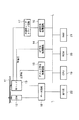
図1は、この実施の形態で説明する光ディスク装置の概略を示している。すなわち、符号11は書き替え可能な光ディスクである。この光ディスク11は、ディスクモータ12によって回転駆動される。そして、この回転状態で、径方向に移動可能に支持された光ヘッド13により、光ディスク11に対して情報の記録または再生が行なわれる。
<Basic description of optical disk device>
FIG. 1 shows an outline of an optical disc apparatus described in this embodiment. That is,
この光ヘッド13は、その内部に設置された半導体レーザから出射されるレーザ光を、光ディスク11の情報記録層に集光させ、その反射光を、後述するPD(Photo Detector)によって受光する。
The
このPDは、その受光領域が、光学的に光ディスク11の径方向に2分割されており、光ヘッド13は、2つの受光領域の各出力信号を加算した和信号と、2つの受光領域の各出力信号の差をとった差信号とを出力する。
In this PD, the light receiving area is optically divided into two in the radial direction of the
そして、光ヘッド13から出力された和信号が、HF(High Frequency)信号処理回路14に供給されることによって、主映像、副映像及び音声等の各種信号が復調される。これらの信号は、光ディスク装置の外部に出力されて映像表示や音声再生に供されるようになり、ここに、光ディスク11に対する情報再生が行なわれる。
The sum signal output from the
また、光ヘッド13から出力された差信号は、ラジアルプッシュプル信号とも称され、所定のトラックのウォブルに対応したウォブル信号となっている。そして、このウォブル信号が、アドレス信号処理回路15に供給されることにより、光ディスク11上の位置を示す物理アドレスが得られる。
The difference signal output from the
一方、光ディスク11に記録すべき情報は、光ディスク装置の外部から記録信号処理回路16に供給される。この記録信号処理回路16は、外部から供給された記録信号を光ディスク11への記録に適したフォーマットに変換し、半導体レーザドライブ回路17に出力する。
On the other hand, information to be recorded on the
そして、この半導体レーザドライブ回路17が、記録信号処理回路16から出力された記録信号に基づいて、光ヘッド13内の半導体レーザを制御することにより、記録信号が光ディスク11に書き込まれ、ここに、光ディスクに対する情報記録が行なわれる。
Then, the semiconductor
なお、上記ディスクモータ12の回転制御、光ヘッド13の光ディスク11の径方向への制御、光ヘッド13内の対物レンズに対するトラッキング方向やフォーカス方向への制御等は、サーボ回路18によって行なわれている。
The
上記した光ディスク11に対する一連の記録再生動作は、CPU(Central Processing Unit)19によって統括的に制御されている。このCPU19は、アドレス信号処理回路15から得られた物理アドレスに基づいて、光ディスク11に対する情報の記録再生位置を制御している。
A series of recording / reproducing operations with respect to the
この場合、CPU19は、ROM20に格納された制御プログラムに基づき、RAM21をワークエリアとして使用しながら、操作部22の操作内容を反映させるように、各回路を制御している。
In this case, the
図2は、上記光ヘッド13における和信号と差信号との生成手段を示している。すなわち、PD23は、前述したように、光学的に光ディスク11の径方向に分割された2つの受光領域23a,23bを備えている。
FIG. 2 shows a means for generating a sum signal and a difference signal in the
そして、一方の受光領域23aからの出力を増幅回路24で増幅した信号と、他方の受光領域23bからの出力を増幅回路25で増幅した信号とを、加算回路26で加算することにより、和信号が生成される。
Then, a signal obtained by amplifying the output from one
また、一方の受光領域23aからの出力を増幅回路24で増幅した信号から、他方の受光領域23bからの出力を増幅回路25で増幅した信号を、減算回路27で減算することにより、差信号が生成される。
Further, the
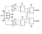
なお、図3に示すように、光ヘッド13内のPD28が、光学的に光ディスク11の径方向に2分割されるとともに、接線方向にも2分割された4つの受光領域28a〜28dを備えている場合もある。
As shown in FIG. 3, the
この場合は、光ディスク11の接線方向に分割された2つの受光領域28a,28bからの各出力を、それぞれ増幅回路29,30で増幅した信号を加算回路31で加算する。また、光ディスク11の接線方向に分割された2つの受光領域28c,28dからの各出力を、それぞれ増幅回路32,33で増幅した信号を加算回路34で加算する。
In this case, the outputs from the two
そして、加算回路31の出力信号と加算回路34の出力信号とを加算回路35で加算することにより、和信号が生成される。また、加算回路31の出力信号から加算回路34の出力信号を減算回路36で減算することにより、差信号が生成される。
The sum signal is generated by adding the output signal of the
〈光ディスクとランドアンドグルーブ記録の説明〉
ここで、上記光ディスク11は、透明基板上に形成された情報記録層の情報記録エリアに、グルーブと呼ばれる案内溝を有している。この案内溝を形成することによりできる凹凸構造はトラックと呼ばれ、情報の記録再生は、このトラックに沿って行なわれる。
<Description of optical disc and land and groove recording>
Here, the
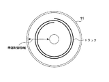
このトラックには、図4に示すように、光ディスク11の内周側から外周側まで連続して繋がるスパイラル型と、複数の同心円から形成される同心円型とがある。
As shown in FIG. 4, the track includes a spiral type continuously connected from the inner peripheral side to the outer peripheral side of the
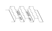
図5及び図6は、トラックを拡大して示している。トラックは、情報記録層の凹凸によって形成されており、一方をグルーブトラック、他方をランドトラックと称している。 5 and 6 show the enlarged track. The track is formed by unevenness of the information recording layer, and one is called a groove track and the other is called a land track.
DVD−RAMでは、図5に示すように、ランドトラックとグルーブトラックとの両方に相変化によるマークを形成して情報を記録可能となっている。また、+RW等では、図6に示すように、グルーブトラックのみに相変化によるマークを形成して情報を記録可能となっている。 In the DVD-RAM, as shown in FIG. 5, information can be recorded by forming marks due to phase change on both the land track and the groove track. In addition, in + RW or the like, as shown in FIG. 6, information can be recorded by forming a mark due to a phase change only on the groove track.
〈ウォブル信号とプッシュプルとの関係の説明〉
図7は、トラックを上面から見た状態を示している。光ディスク11のトラックは、半径方向にわずかに蛇行しており、これをウォブルと称する。このウォブルされたトラックに沿って、集光されたビームスポットを走査していくと、ウォブルの周波数はトラッキングサーボ信号の帯域に比べて高い周波数であるため、ビームスポットはトラックの中心をほぼ直進する。
<Description of relationship between wobble signal and push-pull>
FIG. 7 shows a state in which the track is viewed from above. The track of the
このとき、和信号はほとんど変化せず、半径方向の差信号すなわちラジアルプッシュプル信号のみがウォブルにあわせて変化する。これをウォブル信号と称する。このウォブル信号は、ディスクモータ12の回転周波数の調整や、記録クロックのリファレンス、物理アドレス情報として利用される。
At this time, the sum signal hardly changes, and only the radial difference signal, that is, the radial push-pull signal, changes in accordance with the wobble. This is called a wobble signal. This wobble signal is used as adjustment of the rotation frequency of the
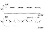
図8(a)は和信号を示し、図8(b)は、差信号つまりラジアルプッシュプル信号(ウォブル信号)を示している。 FIG. 8A shows a sum signal, and FIG. 8B shows a difference signal, that is, a radial push-pull signal (wobble signal).
〈ウォブル信号の説明〉
光ディスク11では、このウォブル信号を変調することによって、光ディスク11の情報記録領域における物理的な位置を示す物理アドレス情報を記録している。
<Description of wobble signal>
The
すなわち、トラックに付与するウォブルに、図9に示すように、互いに周波数の異なる第1周波数と第2周波数との2種類の周波数を切り替える周波数変調を施して物理アドレス情報を記録する手法と、図10に示すように、互いに位相の反転した第1位相と第2位相とを切り替える位相変調を施して物理アドレス情報を記録する手法とがある。 That is, a method of recording physical address information by performing frequency modulation to switch between two types of frequencies, a first frequency and a second frequency, which are different from each other, as shown in FIG. As shown in FIG. 10, there is a method of recording physical address information by performing phase modulation for switching between a first phase and a second phase whose phases are reversed.
記録された物理アドレス情報は、詳細は後述するが、例えば図13に示すような復調回路を用いることで、読み取ることが可能になる。 The recorded physical address information can be read by using, for example, a demodulation circuit as shown in FIG.
図11は、光ディスク11の情報記録領域の構造を示している。光ディスク11では、情報記録領域の物理的な位置を特定するために、記録トラックは、一定長のアドレスセグメント毎に区切られている。各アドレスセグメントには、物理的な位置を示すために、番地等を示す情報がウォブル変調によって予め記録されている。
FIG. 11 shows the structure of the information recording area of the
このウォブル変調によるアドレスセグメントは、例えば図12に示すように構成されている。図12では、アドレスセグメントは複数のアドレスユニットから構成されており、各アドレスユニットは変調領域と無変調領域とからなる。 The address segment by this wobble modulation is configured as shown in FIG. 12, for example. In FIG. 12, the address segment includes a plurality of address units, and each address unit includes a modulation area and a non-modulation area.
そして、変調領域には、アドレス再生のタイミング生成等に用いられる同期パターンやアドレス情報(セグメント、トラック、ゾーン等)がウォブル変調により記録されている。変調領域と無変調領域との割合は、ウォブルの周波数とアドレスセグメントの長さ及びアドレスセグメント当たりに記録されるアドレス情報に依存する。 In the modulation area, a synchronization pattern and address information (segment, track, zone, etc.) used for generating timing of address reproduction and the like are recorded by wobble modulation. The ratio of the modulation area to the non-modulation area depends on the wobble frequency, the length of the address segment, and the address information recorded per address segment.
〈位相復調方法の説明〉
図13は、図1に示した位相変調されたウォブル信号から物理アドレス情報を得るためのアドレス信号処理回路15の一例を示している。ウォブル信号には、記録媒体に固有の雑音や、隣接するトラックに記録されたHF信号からのクロストーク雑音等が含まれている。
<Description of phase demodulation method>
FIG. 13 shows an example of an address
このため、前記減算回路27で生成されたウォブル信号を、BPF(Band Pass Filter)37に通して、ウォブル信号の周波数帯域以外の雑音を取り除く必要がある。この際、位相変化点における波形の周波数は、ウォブル信号の周波数と異なっているため、位相変化点ではBPF処理によって振幅の減衰が生じる。
For this reason, it is necessary to pass the wobble signal generated by the
図14(a)は、減算回路27から出力される位相変調されたウォブル信号を示している。図14(b)は、同図(a)に示すウォブル信号をBPF37に通した信号波形を示している。位相変化点で振幅が減衰しているのがわかる。
FIG. 14A shows a phase-modulated wobble signal output from the
BPF37によって雑音を除去されたウォブル信号は、位相検波回路38に供給されるとともに、搬送波信号を生成するためにPLL(Phase Locked Loop)回路39に入力される。
The wobble signal from which noise has been removed by the
このうち、PLL回路39では、入力されたウォブル信号に対する位相同期処理が行なわれ、ウォブル信号に位相同期した図14(c)に示すような搬送波信号と、ウォブルクロックとが生成される。
Among them, the
また、位相検波回路38では、ウォブル信号とこれに同期した搬送波信号とによって、位相検波処理が行なわれる。ここでは、位相検波処理として、ウォブル信号と搬送波信号とを乗算して位相の極性を判別する手法を用いる。この場合、ウォブル信号は、搬送波信号を乗算することにより、図14(d)に示すように、第1位相と第2位相とでレベルがオフセットされた形で検波される。
The
このため、この位相検波処理によって生じた信号から、LPF40を用いて高周波成分を除去する。そして、LPF40から出力された信号を、スライス回路41によって所定の閾値レベルと比較することで2値化する。
For this reason, a high frequency component is removed from the signal generated by the phase detection process using the
この2値化された波形からアドレスのビット情報を得るには、アドレスビットに同期したクロック(以下シンボルクロックという)が必要となる。アドレスデコーダ42では、PLL回路39から出力されるウォブル周期に同期したウォブルクロックと、スライス回路41から出力される2値化信号とを用いて、シンボルクロックに同期したクロックを生成しアドレスを再生する。
In order to obtain bit information of an address from this binarized waveform, a clock synchronized with the address bit (hereinafter referred to as a symbol clock) is required. The
また、図1に示したアドレス信号処理回路15をデジタル処理で構成する場合は、図15に示すような構成も考えられる。図15において、図13と同一部分には同一符号を付して説明する。すなわち、BPF37を通過したウォブル信号は、A/D(Analog/Digital)コンバータ43によってデジタル信号に変換される。
Further, when the address
このデジタル信号に変換されたウォブル信号は、デジタル処理対応の位相検波回路38及びPLL回路39によって上記と同様に位相検波される。この位相検波された波形は、積分回路44によりウォブルクロック単位で積分処理される。この処理は、LPF40と同様の効果がある。
The wobble signal converted into the digital signal is phase-detected in the same manner as described above by the
そして、積分された波形は、S/H(Sample/Hold)回路45に供給されてウォブルクロックによりサンプルホールドされた後、デジタル処理対応のアドレスデコーダ42に入力されることにより、シンボルクロックに同期したクロックが生成されアドレスが再生される。
The integrated waveform is supplied to an S / H (Sample / Hold)
〈隣接ウォブルによるクロストークの影響〉
しかしながら、記録容量を増加させるために径方向の記録密度を高めた場合、トラックピッチに比べてビームスポット径が相対的に大きくなってしまい、本来走査したいトラックのウォブル信号だけでなく、隣接するトラックのウォブル信号も得られるようになる。これにより、得られたウォブル信号同士が干渉し合い、本来必要とするウォブル信号の振幅や位相に悪影響を及ぼす場合がある。
<Influence of crosstalk by adjacent wobble>
However, if the recording density in the radial direction is increased in order to increase the recording capacity, the beam spot diameter becomes relatively larger than the track pitch, so that not only the wobble signal of the track to be originally scanned but also the adjacent track The wobble signal is also obtained. As a result, the obtained wobble signals may interfere with each other and adversely affect the originally required amplitude and phase of the wobble signal.
例えば、追記型の光ディスク(DVD−R等)のようにCLV方式で記録再生を行なう光ディスクは、半径方向にウォブル位相が揃っていないため、これに該当する。CLV記録再生方式では、図16に示すように、自己トラックと、その内周側及び外周側の隣接トラックとの間で、ウォブルに位相差が生じている。 For example, an optical disc that performs recording and reproduction by the CLV method, such as a write-once optical disc (DVD-R, etc.) corresponds to this because wobble phases are not aligned in the radial direction. In the CLV recording / reproducing system, as shown in FIG. 16, there is a phase difference in wobble between the self track and the adjacent track on the inner and outer peripheral sides.
このウォブルの位相差によって、自己トラックから読み出されたウォブル信号は、隣接トラックのウォブル信号の影響を受け振幅及び位相が変動する。この変動をウォブルビートと称する。 Due to the phase difference of the wobble, the amplitude and phase of the wobble signal read from the self track are affected by the wobble signal of the adjacent track. This fluctuation is called a wobble beat.
内周側ウォブルと自己ウォブルとの位相差をαとした場合、自己ウォブルと外周側ウォブルとの位相差はα+βで表わすことができる。βの値は、ウォブル長とトラックピッチとによって決定される。 When the phase difference between the inner wobble and the self wobble is α, the phase difference between the self wobble and the outer wobble can be expressed as α + β. The value of β is determined by the wobble length and the track pitch.
例えば、ウォブル長WLが9.486μm、トラックピッチTPが0.4μmの光ディスク11においては、
β=2π×(TP/WL)×360
=2π×(0.4/9.486)×360
=95.3deg
となる。
For example, in the
β = 2π × (TP / WL) × 360
= 2π × (0.4 / 9.486) × 360
= 95.3deg
It becomes.
また、αは、最内周トラックのウォブルと、これに隣接するトラックのウォブルとの初期位相差をa0、トラック番号をNによって定義すると
α=a0+[N×(β−1)]deg
と表わすことができる。
Α is defined as a0 and the track number is defined by the initial phase difference between the wobble of the innermost track and the wobble of the adjacent track, and α = a0 + [N × (β-1)] deg
Can be expressed as
この場合、自己トラックと隣接トラックとのウォブルの位相差は、およそトラック4周分の周期で循環することになる。つまり、ウォブルビートの周期はβの値によって決定され、トラック換算では360/βトラックが1周期となる。 In this case, the wobble phase difference between the self track and the adjacent track circulates in a cycle of about four tracks. That is, the wobble beat cycle is determined by the value of β, and 360 / β track is one cycle in track conversion.
ただし、周波数軸上でウォブルビートを観測した場合、ウォブルビートはトラック間のウォブル位相差によって生じるため、トラック長が短くなる光ディスク11の内周側ほどウォブルビートの周波数は高く、外周側ほど低くなる。
However, when the wobble beat is observed on the frequency axis, the wobble beat is caused by the wobble phase difference between the tracks. Therefore, the wobble beat frequency is higher on the inner peripheral side of the
図17(a)〜(c)は、α=90、β=185.3とした場合のウォブル信号の位相関係を示し、図18(a)〜(c)は、隣接トラックからのウォブル信号の干渉を含んだウォブル信号と、そのときの位相検波波形とを示している。 17A to 17C show the phase relationship of the wobble signal when α = 90 and β = 185.3, and FIGS. 18A to 18C show the wobble signal from the adjacent track. A wobble signal including interference and a phase detection waveform at that time are shown.
なお、隣接トラックからのウォブル信号の振幅は、自己トラックのウォブル振幅再生時の30%である。隣接トラックからのウォブルのクロストークにより、第1位相と第2位相のウォブル信号振幅と位相とがそれぞれ影響を受けるため、位相検波波形の信号レベルに非対称性が生じていることがわかる。 Note that the amplitude of the wobble signal from the adjacent track is 30% of the wobble amplitude reproduction of the self track. It can be seen that the wobble signal amplitude and phase of the first phase and the second phase are influenced by the crosstalk of the wobble from the adjacent track, and asymmetry occurs in the signal level of the phase detection waveform.
この場合、図13及び図15に示した構成のアドレス信号処理回路15では、位相検波波形の非対称性を補正する手段を備えていないため、媒体に固有の雑音や隣接トラックに記録されたHF信号の影響等で、ウォブル信号の信号対雑音比が悪化した場合に2値化の判定を誤る可能性が生じる。
In this case, since the address
図19は、αを0〜360degの範囲で変化させた場合のウォブル振幅変動を示し、図20はウォブル位相変動を示し、図21は位相検波波形の変動を示している。図19〜図21において、その右側に記載してある3桁の数字は、それぞれウォブルの変調位相を示している。 19 shows the wobble amplitude fluctuation when α is changed in the range of 0 to 360 deg., FIG. 20 shows the wobble phase fluctuation, and FIG. 21 shows the fluctuation of the phase detection waveform. 19 to 21, the three-digit numbers written on the right side indicate the wobble modulation phase.
例えば、000は内周側隣接トラック、自己トラック、外周側隣接トラックが全て第1位相であること、010は内周側隣接トラックが第1位相、自己トラックが第2位相、外周側隣接トラックが第1位相であることを意味している。 For example, 000 indicates that the inner peripheral side adjacent track, the self track, and the outer peripheral side adjacent track are all in the first phase, 010 indicates that the inner peripheral side adjacent track is in the first phase, the self track is in the second phase, and the outer peripheral side adjacent track is in the first phase. It means that it is the first phase.
これらの変化の周期は、先に記載したβの値に依存し、360/βトラックが1周期となる。図21において、変調領域同士が隣接しないようにウォブルが変調されたアドレスフォーマットであった場合、変調領域での位相検波振幅としては000または010のパターンのみ表われることとなる。 The period of these changes depends on the value of β described above, and 360 / β track is one period. In FIG. 21, when the address format is such that the wobble is modulated so that the modulation areas are not adjacent to each other, only the pattern of 000 or 010 appears as the phase detection amplitude in the modulation area.
この場合、位相検波波形の2値化閾値を補正することで、アドレス検出率を向上させることが可能である。このようなアドレスフォーマットは、図12に示した変調領域と無変調領域との比率において、無変調領域を多くとることで実現が可能である。 In this case, it is possible to improve the address detection rate by correcting the binarization threshold value of the phase detection waveform. Such an address format can be realized by increasing the non-modulation area in the ratio between the modulation area and the non-modulation area shown in FIG.
〈2値化閾値の補正方法〉
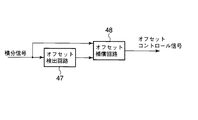
図22は、図1に示した2値化閾値の補正手段を備えたアドレス信号処理回路15を示している。図22において、図15と同一部分には同一符号を付して説明する。すなわち、積分されサンプルホールドされた位相検波波形は、オフセットコントロール回路46に入力される。このオフセットコントロール回路46では、位相検波波形の非対称性を補正している。このことは、2値化閾値を補正することと同等である。
<Binarization threshold correction method>
FIG. 22 shows the address
図23及び図24は、それぞれオフセットコントロール回路46の例を示している。図23はフィードフォーワード型、図24はフィードバック型のオフセットコントロール回路46を示している。
23 and 24 show examples of the offset
図23に示すオフセットコントロール回路46では、オフセット検出回路47で位相検波波形(積分信号)の非対称量を算出し、この算出されたオフセット補償値を用いてオフセット補償回路48で位相検波波形の非対称性を補償している。
In the offset
また、図24に示すオフセットコントロール回路46では、オフセット補償回路49の出力からオフセット検出回路50により非対称量を検出し、その検出されたオフセット補償値をオフセット補償回路49にフィードバックして非対称性を補償している。これらのオフセット補償回路48,49は、減算回路を用いることで簡易に構成することが可能である。
In the offset
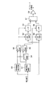
図25は、フィードフォーワード型のオフセットコントロール回路46に使用されるオフセット検出回路47を示している。まず、入力された積分波形の極性を、極性検出回路51により検出する。極性検出回路51から出力される極性信号は、そのままS/H回路52及びLPF53の制御に供されるとともに、ノット回路54を介してS/H回路55及びLPF56の制御に供される。
FIG. 25 shows an offset detection circuit 47 used in the feedforward type offset
これにより、正極性の積分波形振幅がS/H回路52でサンプリングされ、負極性の積分波形振幅がS/H回路55でサンプリングされる。この処理は、ウォブル変調の変調比が異なる場合に必要となる。S/H回路52,55でサンプルホールドされた値は、それぞれLPF53,56を介した後、加算回路57で加算される。
As a result, the positive integrated waveform amplitude is sampled by the S /
このLPF53,56のカットオフ周波数は、ウォブルビートの影響を補正するために光ディスク11の内周側のウォブルビートの周波数帯域よりも高く設定する必要がある。そして、LPF53,56を介し加算された値は、積分波形振幅の非対称補償値となる。この値に増幅回路58によって所定のゲイン調整を施すことにより、オフセット補償値が生成される。
The cut-off frequency of the
図26は、フィードバック型のオフセットコントロール回路46に使用されるオフセット検出回路50を示している。まず、入力された積分波形の極性を、極性検出回路59により検出する。極性検出回路59から出力される極性信号は、そのままS/H回路60の制御に供されるとともに、ノット回路61を介してS/H回路62の制御に供される。
FIG. 26 shows an offset
これにより、正極性の積分波形振幅がS/H回路60でサンプリングされ、負極性の積分波形振幅がS/H回路62でサンプリングされる。これらのS/H回路60,62でサンプルホールドされた両極性の積分波形値を加算回路63で加算した値は、波形の非対称値となる。
As a result, the positive integrated waveform amplitude is sampled by the S /
この非対称値から高周波の雑音成分を除去するために積分回路64を通し、増幅回路65によって所定のゲイン調整をした後出力する。このゲイン調整値は、オフセットコントロール回路46のフィードバック係数となり、オフセットコントロール回路46の制御帯域はこのゲインによって決定される。
In order to remove a high frequency noise component from the asymmetric value, the signal is passed through an
上記したフィードフォーワード型のオフセットコントロール回路46と同様に、フィードバック型のオフセットコントロール回路46の制御帯域も、光ディスク11の内周側のウォブルビート周波数よりも高い帯域に設定する必要がある。具体的には、フィードバック制御系の閉ループ伝達関数より導かれるゲイン特性において、ウォブルビート周波数のゲイン圧縮率が20dB以上あるのが望ましい。
Similar to the feedforward type offset
また、図27及び図28は、それぞれ図25及び図26に示したオフセット検出回路47,50について、ウォブルの変調領域についてのみオフセット補正係数を算出するように変形した回路構成を示している。
27 and 28 show circuit configurations in which the offset
図27及び図28において、それぞれ、図25及び図26と同一部分には同一符号を付して説明すると、変調領域検出回路66,67が新たに追加されている。一般に、ウォブル変調を用いてアドレスを形成する場合、変調領域到来を知らせるためのタイミング信号生成のために所定の同期パターンが記録されている。変調領域検出回路66,67では、この同期パターンを検出することにより、変調領域部分で開、無変調領域部分で閉となるゲート信号を出力する。
In FIGS. 27 and 28, the same reference numerals are given to the same portions as those in FIGS. 25 and 26, and modulation
そして、図27では、アンド回路68,69により、極性信号及びそれをノット回路54によって反転させた信号を、変調領域検出回路66の出力でゲートすることにより、積分信号を変調領域部分でサンプルホールドさせるように制御している。
In FIG. 27, the AND
また、図28では、アンド回路70,71により、極性信号及びそれをノット回路61によって反転させた信号を、変調領域検出回路67の出力でゲートすることにより、積分信号を変調領域部分でサンプルホールドさせるように制御している。さらに、アンド回路70,71の出力をオア回路72でゲートした出力で、積分回路64を駆動させるようにしている。
Also, in FIG. 28, the integration signal is sampled and held in the modulation region portion by gating the polarity signal and the signal obtained by inverting it with the
同期パターンの検出方法としては、FIR(Finite Impulse Response)型のフィルタ等を用いて構成されるマッチドフィルタを用いて、その出力を閾値検出するものが代表的である。このゲート信号と極性検出信号の論理積を後段回路のイネーブル信号とすることで変調領域でのみオフセット補正係数の算出が可能となる。 A typical sync pattern detection method is to detect a threshold value of the output using a matched filter configured using an FIR (Finite Impulse Response) type filter or the like. By calculating the logical product of the gate signal and the polarity detection signal as an enable signal for the subsequent circuit, the offset correction coefficient can be calculated only in the modulation region.
〈2値化閾値の補正の効果〉
図29は、オフセット補正をしない場合の、アドレスデコーダ42に供給される積分波形の例を示し、図30は、オフセット補正をした場合の、アドレスデコーダ42に供給される積分波形の例を示している。
<Effect of binarization threshold correction>
FIG. 29 shows an example of an integrated waveform supplied to the
これらの図より、オフセット補正をすることで波形の非対称性が補正され、閾値レベルである0を境として対称にレベル分布されていることがわかる。アドレスビットは、この積分出力を閾値検出することで復号されるため、0レベルからの距離があるほど信頼性の高い復号が可能となる。 From these figures, it can be seen that the asymmetry of the waveform is corrected by performing the offset correction, and the level distribution is symmetrical with respect to the threshold level of 0. Since the address bits are decoded by detecting the threshold value of this integrated output, the more reliable the distance from the 0 level, the more reliable the decoding is possible.
また、非対称補正を用いることにより、クロストークによる性能劣化を補償することができるため、より光ディスク11のトラックピッチを狭めることが可能となる。一般に、トラックピッチを狭めた場合、隣接トラックのウォブルによるクロストークの影響で、ウォブル信号の信号レベルが減少するのと同時に、隣接トラックに記録されたHF信号が雑音として加わるために雑音レベルが上昇する。
In addition, by using asymmetric correction, it is possible to compensate for performance degradation due to crosstalk, so that the track pitch of the
このうち、隣接トラックのウォブルによるクロストークの影響を、閾値補正によって補償することで、ウォブル信号の信号レベルを確保することが可能となり、閾値補正をしない場合に比べてよりトラックピッチを狭めることができるようになり、記録容量を高めることが可能となる。 Of these, the signal level of the wobble signal can be ensured by compensating for the influence of crosstalk due to the wobble of the adjacent track by threshold correction, and the track pitch can be narrowed more than without threshold correction. As a result, the recording capacity can be increased.
〈非対称補正の流れ〉
図31は、上記した非対称補正動作をまとめたフローチャートを示している。図31において、実線は信号の流れを示し、点線は処理の流れを示している。積分回路44またはLPF40を通過した位相検波波形に対して非対称補正処理が開始されると、まず、変調領域の検出がなされる。
<Asymmetric correction flow>
FIG. 31 shows a flowchart summarizing the asymmetric correction operation described above. In FIG. 31, a solid line indicates a signal flow, and a dotted line indicates a processing flow. When the asymmetric correction processing is started on the phase detection waveform that has passed through the
一般に、ウォブル変調を用いてアドレスを形成する場合、変調領域の到来を知らせるためのタイミング信号生成のために、所定の同期パターンが記録されている。変調領域は、この同期パターンやアドレス記録部より検出する。 Generally, when an address is formed using wobble modulation, a predetermined synchronization pattern is recorded for generating a timing signal for notifying the arrival of a modulation area. The modulation area is detected from the synchronization pattern and the address recording unit.
また、同期パターンやアドレス記録部の到来タイミングに周期性がある場合には、これを利用することもできる。現在の波形が無変調領域のものであった場合、非対称量の検出は行なわずに、前のステップおいて求められた非対称量を用いて入力波形に対する非対称補正処理を行なう。 Further, when there is periodicity in the arrival timing of the synchronization pattern or the address recording unit, this can be used. If the current waveform is in the non-modulation region, the asymmetry correction processing is performed on the input waveform using the asymmetry obtained in the previous step without detecting the asymmetry.
変調領域の波形であった場合には、波形の極性判別をする。波形が正極性の場合には、その振幅値を検出し保持する。また、波形が負極性の場合には、その振幅値を検出し保持する。波形極性のデューティー比が、非対称補正制御を行なう帯域において50対50であった場合、極性検出の必要はなくなる。次に、各極性の保持された振幅値より非対称量を計算し記録する。最後に記録された非対称量の値を用いて非対称補正をし、波形を出力する。 If the waveform is in the modulation region, the polarity of the waveform is determined. When the waveform is positive, the amplitude value is detected and held. When the waveform is negative, the amplitude value is detected and held. When the duty ratio of the waveform polarity is 50 to 50 in the band where the asymmetry correction control is performed, it is not necessary to detect the polarity. Next, the amount of asymmetry is calculated and recorded from the amplitude value held for each polarity. Finally, the asymmetry correction is performed using the value of the asymmetry amount recorded, and a waveform is output.
なお、この発明は上記した実施の形態そのままに限定されるものではなく、実施段階ではその要旨を逸脱しない範囲で構成要素を種々変形して具体化することができる。また、上記した実施の形態に開示されている複数の構成要素を適宜に組み合わせることにより、種々の発明を形成することができる。例えば、実施の形態に示される全構成要素からいくつかの構成要素を削除しても良いものである。 Note that the present invention is not limited to the above-described embodiments as they are, and can be embodied by variously modifying the constituent elements without departing from the scope of the invention in the implementation stage. Various inventions can be formed by appropriately combining a plurality of constituent elements disclosed in the above-described embodiments. For example, some components may be deleted from all the components shown in the embodiment.
11…光ディスク、12…ディスクモータ、13…光ヘッド、14…HF信号処理回路、15…アドレス信号処理回路、16…記録信号処理回路、17…半導体レーザドライブ回路、18…サーボ回路、19…CPU、20…ROM、21…RAM、22…操作部、23…PD、24,25…増幅回路、26…加算回路、27…減算回路、28…PD、29,30…増幅回路、31…加算回路、32,33…増幅回路、34,35…加算回路、36…減算回路、37…BPF、38…位相検波回路、39…PLL回路、40…LPF、41…スライス回路、42…アドレスデコーダ、43…A/Dコンバータ、44…積分回路、45…S/H回路、46…オフセットコントロール回路、47…オフセット検出回路、48,49…オフセット補償回路、50…オフセット検出回路、51…極性検出回路、52…S/H回路、53…LPF、54…ノット回路、55…S/H回路、56…LPF、57…加算回路、58…増幅回路、59…極性検出回路、60…S/H回路、61…ノット回路、62…S/H回路、63…加算回路、64…積分回路、65…増幅回路、66,67…変調領域検出回路、68〜71…アンド回路、72…オア回路。
DESCRIPTION OF
Claims (10)
このウォブル信号読み取り手段で読み取られたウォブル信号に位相検波処理を施し、得られた位相検波信号の振幅を所定の閾値と比較することにより2値化して、前記アドレス情報を再生するアドレス情報再生手段と、
前記ウォブル信号読み取り手段による前記所定のトラックからのウォブル信号の読み取り時に、前記アドレス情報再生手段で得られた位相検波信号に生じる振幅の非対称性を、前記所定の閾値に対して補正する補正手段とを具備したことを特徴とする光ディスク再生装置。 Wobble signal reading means for reading a signal corresponding to the wobble formed on a predetermined track from the optical disk on which address information is recorded by phase-modulating the wobble formed on the track;
Address information reproducing means for performing phase detection processing on the wobble signal read by the wobble signal reading means, binarizing the obtained phase detection signal by comparing it with a predetermined threshold value, and reproducing the address information When,
Correction means for correcting amplitude asymmetry generated in the phase detection signal obtained by the address information reproducing means when the wobble signal reading means reads the wobble signal from the predetermined track with respect to the predetermined threshold; An optical disc reproducing apparatus comprising:
前記アドレス情報再生手段で得られた位相検波信号の振幅の非対称量を算出するオフセット検出手段と、
このオフセット検出手段で算出された非対称量に基づいて、前記位相検波信号の振幅の非対称性を補償するオフセット補償手段とを具備したことを特徴とする請求項1記載の光ディスク再生装置。 The correction means includes
Offset detecting means for calculating an asymmetry amount of amplitude of the phase detection signal obtained by the address information reproducing means;
2. The optical disk reproducing apparatus according to claim 1, further comprising offset compensating means for compensating for the asymmetry of the amplitude of the phase detection signal based on the amount of asymmetry calculated by the offset detecting means.
前記アドレス情報再生手段で得られた位相検波信号の正負の極性を検出する極性検出手段と、
この極性検出手段により前記位相検波信号の正極性が検出された状態で、前記位相検波信号の振幅を保持する第1の保持手段と、
この第1の保持手段の出力信号から高周波成分を除去する第1のフィルタと、
前記極性検出手段により前記位相検波信号の負極性が検出された状態で、前記位相検波信号の振幅を保持する第2の保持手段と、
この第2の保持手段の出力信号から高周波成分を除去する第2のフィルタと、
前記第1のフィルタの出力信号と前記第2のフィルタの出力信号とを加算して、前記位相検波信号の振幅の非対称量を算出する加算手段とを具備したことを特徴とする請求項2記載の光ディスク再生装置。 The offset detection means includes
Polarity detection means for detecting the polarity of the phase detection signal obtained by the address information reproduction means;
First holding means for holding the amplitude of the phase detection signal in a state where the polarity of the phase detection signal is detected by the polarity detection means;
A first filter for removing high frequency components from the output signal of the first holding means;
Second holding means for holding the amplitude of the phase detection signal in a state where the negative polarity of the phase detection signal is detected by the polarity detection means;
A second filter for removing high-frequency components from the output signal of the second holding means;
3. An adding means for adding an output signal of the first filter and an output signal of the second filter to calculate an amplitude asymmetry of the phase detection signal. Optical disk playback device.
前記ウォブル信号読み取り手段で読み取られたウォブル信号の位相変調領域を検出する変調領域検出手段と、
この変調領域検出手段の検出結果に基づいて前記第1の保持手段及び前記第2の保持手段の保持動作を制御する制御手段とを具備したことを特徴とする請求項3記載の光ディスク再生装置。 The offset detection means includes
A modulation area detecting means for detecting a phase modulation area of the wobble signal read by the wobble signal reading means;
4. An optical disk reproducing apparatus according to claim 3, further comprising a control means for controlling a holding operation of the first holding means and the second holding means based on a detection result of the modulation area detecting means.
前記アドレス情報再生手段で得られた位相検波信号の振幅の非対称量に基づいて、前記位相検波信号の振幅の非対称性を補償するオフセット補償手段と、
このオフセット補償手段から出力される前記位相検波信号の振幅の非対称量を算出し、前記オフセット補償手段にフィードバックするオフセット検出手段とを具備したことを特徴とする請求項1記載の光ディスク再生装置。 The correction means includes
Offset compensation means for compensating for the amplitude asymmetry of the phase detection signal based on the amplitude asymmetry of the phase detection signal obtained by the address information reproducing means;
2. An optical disk reproducing apparatus according to claim 1, further comprising offset detecting means for calculating an asymmetry amount of the amplitude of the phase detection signal output from the offset compensating means and feeding back to the offset compensating means.
前記アドレス情報再生手段で得られた位相検波信号の正負の極性を検出する極性検出手段と、
この極性検出手段により前記位相検波信号の正極性が検出された状態で、前記位相検波信号の振幅を保持する第1の保持手段と、
前記極性検出手段により前記位相検波信号の負極性が検出された状態で、前記位相検波信号の振幅を保持する第2の保持手段と、
前記第1の保持手段に保持された振幅と前記第2の保持手段に保持された振幅とを加算する加算手段と、
この加算手段の出力信号に積分処理を施して、前記位相検波信号の振幅の非対称量を算出する積分手段とを具備したことを特徴とする請求項5記載の光ディスク再生装置。 The offset detection means includes
Polarity detection means for detecting the polarity of the phase detection signal obtained by the address information reproduction means;
First holding means for holding the amplitude of the phase detection signal in a state where the polarity of the phase detection signal is detected by the polarity detection means;
Second holding means for holding the amplitude of the phase detection signal in a state where the negative polarity of the phase detection signal is detected by the polarity detection means;
Adding means for adding the amplitude held in the first holding means and the amplitude held in the second holding means;
6. The optical disk reproducing apparatus according to claim 5, further comprising an integrating unit that performs an integration process on the output signal of the adding unit to calculate an asymmetry amount of the amplitude of the phase detection signal.
前記ウォブル信号読み取り手段で読み取られたウォブル信号の位相変調領域を検出する変調領域検出手段と、
この変調領域検出手段の検出結果に基づいて前記第1の保持手段及び前記第2の保持手段の駆動を制御する第1の制御手段と、
この第1の制御手段の制御により前記第1の保持手段または前記第2の保持手段が駆動された状態で、前記積分手段を駆動させる第2の制御手段とを具備したことを特徴とする請求項6記載の光ディスク再生装置。 The offset detection means includes
A modulation area detecting means for detecting a phase modulation area of the wobble signal read by the wobble signal reading means;
First control means for controlling the driving of the first holding means and the second holding means based on the detection result of the modulation area detecting means;
And a second control means for driving the integration means in a state where the first holding means or the second holding means is driven by the control of the first control means. Item 7. The optical disk playback device according to Item 6.
読み取ったウォブル信号に位相検波処理を施し、得られた位相検波信号の振幅を所定の閾値と比較することにより2値化して、前記アドレス情報を再生する工程と、
前記所定のトラックからのウォブル信号の読み取り時に、前記位相検波信号に生じる振幅の非対称性を、前記所定の閾値に対して補正する工程とを具備したことを特徴とする光ディスク再生方法。 Reading a signal corresponding to the wobble formed on a predetermined track from an optical disk on which address information is recorded by phase-modulating the wobble formed on the track;
Performing a phase detection process on the read wobble signal, binarizing the obtained phase detection signal by comparing it with a predetermined threshold value, and reproducing the address information;
An optical disk reproducing method comprising: correcting amplitude asymmetry generated in the phase detection signal with respect to the predetermined threshold when reading a wobble signal from the predetermined track.
ウォブル信号の位相変調領域を検出する工程と、
位相変調領域が検出された状態で前記位相検波信号の正負の極性を検出する工程と、
正極性が検出された状態で前記位相検波信号の振幅を保持する工程と、
負極性が検出された状態で前記位相検波信号の振幅を保持する工程と、
保持された正極性の振幅と負極制の振幅とに基づいて前記位相検波信号の振幅の非対称量を算出する工程と、
算出された非対称量に基づいて前記位相検波信号の振幅の非対称性を補償する工程とを具備したことを特徴とする請求項9記載の光ディスク再生方法。 The correcting step includes
Detecting a phase modulation region of the wobble signal;
Detecting a positive / negative polarity of the phase detection signal in a state where a phase modulation region is detected;
Maintaining the amplitude of the phase detection signal in a state where positive polarity is detected;
Maintaining the amplitude of the phase detection signal in a state where negative polarity is detected;
Calculating an asymmetry amount of the amplitude of the phase detection signal based on the held positive polarity amplitude and negative polarity amplitude;
10. The optical disk reproducing method according to claim 9, further comprising a step of compensating for the asymmetry of the amplitude of the phase detection signal based on the calculated asymmetry amount.
Priority Applications (3)
| Application Number | Priority Date | Filing Date | Title |
|---|---|---|---|
| JP2003318392A JP4095514B2 (en) | 2003-09-10 | 2003-09-10 | Optical disc playback apparatus and optical disc playback method |
| US10/935,183 US7342864B2 (en) | 2003-09-10 | 2004-09-08 | Optical disk reproduction apparatus and optical disk reproduction method |
| CN200410077135.4A CN1288642C (en) | 2003-09-10 | 2004-09-10 | Optical disc reproducing device and optical disc reproducing method |
Applications Claiming Priority (1)
| Application Number | Priority Date | Filing Date | Title |
|---|---|---|---|
| JP2003318392A JP4095514B2 (en) | 2003-09-10 | 2003-09-10 | Optical disc playback apparatus and optical disc playback method |
Publications (3)
| Publication Number | Publication Date |
|---|---|
| JP2005085407A JP2005085407A (en) | 2005-03-31 |
| JP2005085407A5 JP2005085407A5 (en) | 2006-04-13 |
| JP4095514B2 true JP4095514B2 (en) | 2008-06-04 |
Family
ID=34417687
Family Applications (1)
| Application Number | Title | Priority Date | Filing Date |
|---|---|---|---|
| JP2003318392A Expired - Fee Related JP4095514B2 (en) | 2003-09-10 | 2003-09-10 | Optical disc playback apparatus and optical disc playback method |
Country Status (3)
| Country | Link |
|---|---|
| US (1) | US7342864B2 (en) |
| JP (1) | JP4095514B2 (en) |
| CN (1) | CN1288642C (en) |
Families Citing this family (8)
| Publication number | Priority date | Publication date | Assignee | Title |
|---|---|---|---|---|
| KR100675355B1 (en) * | 2005-02-18 | 2007-01-29 | 삼성전자주식회사 | Method for correcting wave form level with considering asymmetric fine error and system thereof |
| US7738326B2 (en) * | 2005-04-13 | 2010-06-15 | Nec Corporation | Signal processing method of wobble signal, recording and reproducing method of optical disc, optical disc apparatus, program, and recording medium |
| US7821889B1 (en) * | 2006-05-11 | 2010-10-26 | Marvell International Ltd. | Offset loop for wobble |
| US8355302B1 (en) * | 2006-05-11 | 2013-01-15 | Marvell International Ltd. | Offset loop for wobble |
| JP4501902B2 (en) * | 2006-06-30 | 2010-07-14 | 日本ビクター株式会社 | Optical disc recording / reproducing apparatus and optical disc recording / reproducing method |
| JP4501934B2 (en) * | 2006-12-28 | 2010-07-14 | 日本ビクター株式会社 | Optical disc recording / reproducing apparatus and recording / reproducing method thereof |
| JP2010049746A (en) * | 2008-08-21 | 2010-03-04 | Sony Corp | Demodulating apparatus, demodulating method, information reproducing apparatus, and computer program |
| US8582405B1 (en) * | 2012-09-25 | 2013-11-12 | Oracle International Corporation | Matched pattern signal decoding |
Family Cites Families (8)
| Publication number | Priority date | Publication date | Assignee | Title |
|---|---|---|---|---|
| US6069870A (en) * | 1996-10-22 | 2000-05-30 | Hitachi, Ltd. | Information recording medium which indicates information according to the wobbling of a track and information recording and reproducing apparatus |
| CN1206904A (en) | 1997-05-20 | 1999-02-03 | 先锋株式会社 | Pre concave groove testing device and method |
| JP3938449B2 (en) | 1999-06-02 | 2007-06-27 | パイオニア株式会社 | Optical disc recording method, optical disc recording apparatus, optical disc, and optical disc reproducing apparatus |
| US6345018B1 (en) * | 1999-08-04 | 2002-02-05 | Ricoh Company, Ltd. | Demodulation circuit for demodulating wobbling signal |
| JP2001209937A (en) | 2000-01-27 | 2001-08-03 | Ricoh Co Ltd | Demodulation device and information recording/ reproducing device |
| US6912190B2 (en) * | 2000-11-15 | 2005-06-28 | Matsushita Electric Industrial Co., Ltd. | Optical disc apparatus and method for reading information from an optical disk having tracks and spaces between the tracks on which address information is recorded |
| US6809997B2 (en) * | 2001-11-17 | 2004-10-26 | Lg Electronics Inc. | Apparatus and method for detecting wobble signal read from optical disc |
| US7200080B2 (en) * | 2002-01-16 | 2007-04-03 | Yamaha Corporation | Optical disk recorder with reproduction quality control |
-
2003
- 2003-09-10 JP JP2003318392A patent/JP4095514B2/en not_active Expired - Fee Related
-
2004
- 2004-09-08 US US10/935,183 patent/US7342864B2/en not_active Expired - Fee Related
- 2004-09-10 CN CN200410077135.4A patent/CN1288642C/en not_active Expired - Fee Related
Also Published As
| Publication number | Publication date |
|---|---|
| CN1595502A (en) | 2005-03-16 |
| US7342864B2 (en) | 2008-03-11 |
| CN1288642C (en) | 2006-12-06 |
| US20050094515A1 (en) | 2005-05-05 |
| JP2005085407A (en) | 2005-03-31 |
Similar Documents
| Publication | Publication Date | Title |
|---|---|---|
| US7333408B2 (en) | Demodulator, disk drive device, and phase adjustment method | |
| EP1184850A2 (en) | Recording and/or reproducing apparatus and recording and/or reproducing method capable of detecting a land pre-pit on disc securely at a high precision | |
| JP2000099952A (en) | Optical disk and optical disk device | |
| JP3929207B2 (en) | Pre-pit detection device for optical recording medium | |
| JP4095514B2 (en) | Optical disc playback apparatus and optical disc playback method | |
| US6639882B2 (en) | Pre-pit detecting apparatus | |
| JP2002074678A (en) | Optical recording medium | |
| JP4317810B2 (en) | Optical disc recording / reproducing apparatus | |
| JP4775378B2 (en) | Optical disc signal reproduction method and optical disc apparatus | |
| JP4403344B2 (en) | Disk drive device | |
| JP3714117B2 (en) | Pre-pit detection device, pre-pit detection method, position and frequency signal detection circuit | |
| JP4172494B2 (en) | Demodulation device, disk drive device, and demodulation method | |
| JP3797074B2 (en) | Recording and / or reproducing apparatus and method | |
| JP4403393B2 (en) | Demodulation device, disk drive device, and demodulation method | |
| JP4442342B2 (en) | Integral phase determination method, demodulation method, demodulation device, disk drive device | |
| JP4618454B2 (en) | Timing signal generator | |
| JP2005158168A (en) | Information reading device and prepit detecting circuit | |
| WO2005101388A1 (en) | Optical disc recording/reproduction device | |
| JP3876601B2 (en) | Land pre-pit detection device and optical disk device using the same | |
| JP2002367185A (en) | Optical disk device | |
| JP3921435B2 (en) | Optical disk device, optimal radial tilt or optimal track offset calculation method | |
| JP2004087029A (en) | Optical disk and optical disk device | |
| JP2009158052A (en) | Optical disk processing apparatus and optical disk processing method | |
| JP2007035145A (en) | Optical disk processing device and optical disk processing method | |
| JP2006338716A (en) | Pll circuit and optical disk drive using it |
Legal Events
| Date | Code | Title | Description |
|---|---|---|---|
| A521 | Request for written amendment filed |
Free format text: JAPANESE INTERMEDIATE CODE: A523 Effective date: 20060224 |
|
| A621 | Written request for application examination |
Free format text: JAPANESE INTERMEDIATE CODE: A621 Effective date: 20060224 |
|
| A977 | Report on retrieval |
Free format text: JAPANESE INTERMEDIATE CODE: A971007 Effective date: 20080225 |
|
| TRDD | Decision of grant or rejection written | ||
| A01 | Written decision to grant a patent or to grant a registration (utility model) |
Free format text: JAPANESE INTERMEDIATE CODE: A01 Effective date: 20080304 |
|
| A61 | First payment of annual fees (during grant procedure) |
Free format text: JAPANESE INTERMEDIATE CODE: A61 Effective date: 20080307 |
|
| FPAY | Renewal fee payment (event date is renewal date of database) |
Free format text: PAYMENT UNTIL: 20110314 Year of fee payment: 3 |
|
| FPAY | Renewal fee payment (event date is renewal date of database) |
Free format text: PAYMENT UNTIL: 20110314 Year of fee payment: 3 |
|
| FPAY | Renewal fee payment (event date is renewal date of database) |
Free format text: PAYMENT UNTIL: 20120314 Year of fee payment: 4 |
|
| LAPS | Cancellation because of no payment of annual fees |