JP4086023B2 - Micromechanical electrostatic vibrator - Google Patents
Micromechanical electrostatic vibrator Download PDFInfo
- Publication number
- JP4086023B2 JP4086023B2 JP2004244835A JP2004244835A JP4086023B2 JP 4086023 B2 JP4086023 B2 JP 4086023B2 JP 2004244835 A JP2004244835 A JP 2004244835A JP 2004244835 A JP2004244835 A JP 2004244835A JP 4086023 B2 JP4086023 B2 JP 4086023B2
- Authority
- JP
- Japan
- Prior art keywords
- vibrating body
- substrate
- vibrator
- electrode
- vibration
- Prior art date
- Legal status (The legal status is an assumption and is not a legal conclusion. Google has not performed a legal analysis and makes no representation as to the accuracy of the status listed.)
- Expired - Fee Related
Links
- 230000008859 change Effects 0.000 claims abstract description 16
- 239000000758 substrate Substances 0.000 claims description 202
- 230000005284 excitation Effects 0.000 claims description 124
- XUIMIQQOPSSXEZ-UHFFFAOYSA-N Silicon Chemical compound [Si] XUIMIQQOPSSXEZ-UHFFFAOYSA-N 0.000 claims description 50
- 229910052710 silicon Inorganic materials 0.000 claims description 50
- 239000010703 silicon Substances 0.000 claims description 50
- 239000012212 insulator Substances 0.000 claims description 24
- 239000011521 glass Substances 0.000 claims description 23
- 150000003377 silicon compounds Chemical class 0.000 claims description 2
- 239000010410 layer Substances 0.000 description 191
- 238000000034 method Methods 0.000 description 67
- 230000008569 process Effects 0.000 description 36
- 238000006073 displacement reaction Methods 0.000 description 34
- 230000002829 reductive effect Effects 0.000 description 31
- 238000004519 manufacturing process Methods 0.000 description 30
- 239000010408 film Substances 0.000 description 28
- 230000000052 comparative effect Effects 0.000 description 24
- 239000000463 material Substances 0.000 description 21
- 239000004065 semiconductor Substances 0.000 description 21
- 238000005530 etching Methods 0.000 description 18
- 230000003071 parasitic effect Effects 0.000 description 16
- 229910021420 polycrystalline silicon Inorganic materials 0.000 description 16
- 239000004020 conductor Substances 0.000 description 15
- 230000008602 contraction Effects 0.000 description 15
- 229920005591 polysilicon Polymers 0.000 description 15
- 238000005452 bending Methods 0.000 description 14
- VYPSYNLAJGMNEJ-UHFFFAOYSA-N silicon dioxide Inorganic materials O=[Si]=O VYPSYNLAJGMNEJ-UHFFFAOYSA-N 0.000 description 14
- 238000009826 distribution Methods 0.000 description 10
- 230000007423 decrease Effects 0.000 description 9
- 229910004298 SiO 2 Inorganic materials 0.000 description 7
- 230000015572 biosynthetic process Effects 0.000 description 7
- 239000000919 ceramic Substances 0.000 description 7
- 238000005229 chemical vapour deposition Methods 0.000 description 7
- 238000005516 engineering process Methods 0.000 description 7
- 238000000206 photolithography Methods 0.000 description 7
- 235000012239 silicon dioxide Nutrition 0.000 description 7
- 238000004544 sputter deposition Methods 0.000 description 7
- 229910052782 aluminium Inorganic materials 0.000 description 6
- XAGFODPZIPBFFR-UHFFFAOYSA-N aluminium Chemical compound [Al] XAGFODPZIPBFFR-UHFFFAOYSA-N 0.000 description 6
- 239000012071 phase Substances 0.000 description 6
- 229920002120 photoresistant polymer Polymers 0.000 description 6
- 239000010453 quartz Substances 0.000 description 6
- 229920003002 synthetic resin Polymers 0.000 description 6
- 239000000057 synthetic resin Substances 0.000 description 6
- OAICVXFJPJFONN-UHFFFAOYSA-N Phosphorus Chemical compound [P] OAICVXFJPJFONN-UHFFFAOYSA-N 0.000 description 5
- 238000010586 diagram Methods 0.000 description 5
- 230000005484 gravity Effects 0.000 description 5
- 229910052751 metal Inorganic materials 0.000 description 5
- 239000002184 metal Substances 0.000 description 5
- 229910052698 phosphorus Inorganic materials 0.000 description 5
- 239000011574 phosphorus Substances 0.000 description 5
- 238000012545 processing Methods 0.000 description 5
- 239000000470 constituent Substances 0.000 description 4
- 230000003247 decreasing effect Effects 0.000 description 4
- 238000011161 development Methods 0.000 description 4
- 239000011347 resin Substances 0.000 description 4
- 229920005989 resin Polymers 0.000 description 4
- 239000000377 silicon dioxide Substances 0.000 description 4
- 229910001218 Gallium arsenide Inorganic materials 0.000 description 3
- -1 Si 3 N 4 Chemical compound 0.000 description 3
- 230000008901 benefit Effects 0.000 description 3
- 238000004891 communication Methods 0.000 description 3
- 238000001514 detection method Methods 0.000 description 3
- 238000001704 evaporation Methods 0.000 description 3
- 238000010438 heat treatment Methods 0.000 description 3
- 238000012986 modification Methods 0.000 description 3
- 230000004048 modification Effects 0.000 description 3
- 238000000059 patterning Methods 0.000 description 3
- 230000002093 peripheral effect Effects 0.000 description 3
- 239000011148 porous material Substances 0.000 description 3
- 239000011241 protective layer Substances 0.000 description 3
- 238000003980 solgel method Methods 0.000 description 3
- 239000004925 Acrylic resin Substances 0.000 description 2
- 229920000178 Acrylic resin Polymers 0.000 description 2
- RYGMFSIKBFXOCR-UHFFFAOYSA-N Copper Chemical compound [Cu] RYGMFSIKBFXOCR-UHFFFAOYSA-N 0.000 description 2
- 241001442234 Cosa Species 0.000 description 2
- 244000126211 Hericium coralloides Species 0.000 description 2
- 229910052581 Si3N4 Inorganic materials 0.000 description 2
- 229910010413 TiO 2 Inorganic materials 0.000 description 2
- 238000013459 approach Methods 0.000 description 2
- 238000005513 bias potential Methods 0.000 description 2
- 239000003990 capacitor Substances 0.000 description 2
- 238000000576 coating method Methods 0.000 description 2
- 150000001875 compounds Chemical class 0.000 description 2
- 229910052802 copper Inorganic materials 0.000 description 2
- 239000010949 copper Substances 0.000 description 2
- 239000013078 crystal Substances 0.000 description 2
- 238000001312 dry etching Methods 0.000 description 2
- 235000013372 meat Nutrition 0.000 description 2
- 229910044991 metal oxide Inorganic materials 0.000 description 2
- 150000004706 metal oxides Chemical class 0.000 description 2
- HQVNEWCFYHHQES-UHFFFAOYSA-N silicon nitride Chemical compound N12[Si]34N5[Si]62N3[Si]51N64 HQVNEWCFYHHQES-UHFFFAOYSA-N 0.000 description 2
- LFQSCWFLJHTTHZ-UHFFFAOYSA-N Ethanol Chemical compound CCO LFQSCWFLJHTTHZ-UHFFFAOYSA-N 0.000 description 1
- 229910000577 Silicon-germanium Inorganic materials 0.000 description 1
- 229910021417 amorphous silicon Inorganic materials 0.000 description 1
- 238000004458 analytical method Methods 0.000 description 1
- 230000005540 biological transmission Effects 0.000 description 1
- 238000004364 calculation method Methods 0.000 description 1
- 239000011248 coating agent Substances 0.000 description 1
- 238000001035 drying Methods 0.000 description 1
- 230000000694 effects Effects 0.000 description 1
- 238000000227 grinding Methods 0.000 description 1
- 238000009499 grossing Methods 0.000 description 1
- 238000009616 inductively coupled plasma Methods 0.000 description 1
- 238000003780 insertion Methods 0.000 description 1
- 230000037431 insertion Effects 0.000 description 1
- 239000011810 insulating material Substances 0.000 description 1
- 238000009413 insulation Methods 0.000 description 1
- 239000007788 liquid Substances 0.000 description 1
- 239000004973 liquid crystal related substance Substances 0.000 description 1
- 238000004518 low pressure chemical vapour deposition Methods 0.000 description 1
- 230000000873 masking effect Effects 0.000 description 1
- 238000005459 micromachining Methods 0.000 description 1
- 230000003647 oxidation Effects 0.000 description 1
- 238000007254 oxidation reaction Methods 0.000 description 1
- 235000011837 pasties Nutrition 0.000 description 1
- 230000000149 penetrating effect Effects 0.000 description 1
- 238000005268 plasma chemical vapour deposition Methods 0.000 description 1
- 238000005498 polishing Methods 0.000 description 1
- 238000007639 printing Methods 0.000 description 1
- 238000011160 research Methods 0.000 description 1
- 230000004044 response Effects 0.000 description 1
- 239000002904 solvent Substances 0.000 description 1
- 238000004528 spin coating Methods 0.000 description 1
- 230000007480 spreading Effects 0.000 description 1
- 238000003892 spreading Methods 0.000 description 1
- 238000000992 sputter etching Methods 0.000 description 1
- 230000003068 static effect Effects 0.000 description 1
- 239000000126 substance Substances 0.000 description 1
- 239000010409 thin film Substances 0.000 description 1
- 238000007740 vapor deposition Methods 0.000 description 1
- 238000001947 vapour-phase growth Methods 0.000 description 1
- 239000013585 weight reducing agent Substances 0.000 description 1
- 238000001039 wet etching Methods 0.000 description 1
Images


Classifications
-
- H—ELECTRICITY
- H03—ELECTRONIC CIRCUITRY
- H03H—IMPEDANCE NETWORKS, e.g. RESONANT CIRCUITS; RESONATORS
- H03H9/00—Networks comprising electromechanical or electro-acoustic devices; Electromechanical resonators
- H03H9/24—Constructional features of resonators of material which is not piezoelectric, electrostrictive, or magnetostrictive
- H03H9/2405—Constructional features of resonators of material which is not piezoelectric, electrostrictive, or magnetostrictive of microelectro-mechanical resonators
- H03H9/2431—Ring resonators
-
- H—ELECTRICITY
- H03—ELECTRONIC CIRCUITRY
- H03H—IMPEDANCE NETWORKS, e.g. RESONANT CIRCUITS; RESONATORS
- H03H3/00—Apparatus or processes specially adapted for the manufacture of impedance networks, resonating circuits, resonators
- H03H3/007—Apparatus or processes specially adapted for the manufacture of impedance networks, resonating circuits, resonators for the manufacture of electromechanical resonators or networks
- H03H3/0072—Apparatus or processes specially adapted for the manufacture of impedance networks, resonating circuits, resonators for the manufacture of electromechanical resonators or networks of microelectro-mechanical resonators or networks
-
- H—ELECTRICITY
- H03—ELECTRONIC CIRCUITRY
- H03H—IMPEDANCE NETWORKS, e.g. RESONANT CIRCUITS; RESONATORS
- H03H9/00—Networks comprising electromechanical or electro-acoustic devices; Electromechanical resonators
- H03H9/02—Details
- H03H9/02244—Details of microelectro-mechanical resonators
- H03H9/02259—Driving or detection means
-
- H—ELECTRICITY
- H03—ELECTRONIC CIRCUITRY
- H03H—IMPEDANCE NETWORKS, e.g. RESONANT CIRCUITS; RESONATORS
- H03H9/00—Networks comprising electromechanical or electro-acoustic devices; Electromechanical resonators
- H03H9/02—Details
- H03H9/02244—Details of microelectro-mechanical resonators
- H03H9/02433—Means for compensation or elimination of undesired effects
-
- H—ELECTRICITY
- H03—ELECTRONIC CIRCUITRY
- H03H—IMPEDANCE NETWORKS, e.g. RESONANT CIRCUITS; RESONATORS
- H03H9/00—Networks comprising electromechanical or electro-acoustic devices; Electromechanical resonators
- H03H9/02—Details
- H03H9/05—Holders; Supports
- H03H9/10—Mounting in enclosures
- H03H9/1057—Mounting in enclosures for microelectro-mechanical devices
-
- H—ELECTRICITY
- H03—ELECTRONIC CIRCUITRY
- H03H—IMPEDANCE NETWORKS, e.g. RESONANT CIRCUITS; RESONATORS
- H03H9/00—Networks comprising electromechanical or electro-acoustic devices; Electromechanical resonators
- H03H9/24—Constructional features of resonators of material which is not piezoelectric, electrostrictive, or magnetostrictive
- H03H9/2405—Constructional features of resonators of material which is not piezoelectric, electrostrictive, or magnetostrictive of microelectro-mechanical resonators
- H03H9/2436—Disk resonators
-
- H—ELECTRICITY
- H03—ELECTRONIC CIRCUITRY
- H03H—IMPEDANCE NETWORKS, e.g. RESONANT CIRCUITS; RESONATORS
- H03H9/00—Networks comprising electromechanical or electro-acoustic devices; Electromechanical resonators
- H03H9/24—Constructional features of resonators of material which is not piezoelectric, electrostrictive, or magnetostrictive
- H03H9/2405—Constructional features of resonators of material which is not piezoelectric, electrostrictive, or magnetostrictive of microelectro-mechanical resonators
- H03H9/2447—Beam resonators
- H03H9/2457—Clamped-free beam resonators
-
- H—ELECTRICITY
- H03—ELECTRONIC CIRCUITRY
- H03H—IMPEDANCE NETWORKS, e.g. RESONANT CIRCUITS; RESONATORS
- H03H9/00—Networks comprising electromechanical or electro-acoustic devices; Electromechanical resonators
- H03H9/24—Constructional features of resonators of material which is not piezoelectric, electrostrictive, or magnetostrictive
- H03H9/2405—Constructional features of resonators of material which is not piezoelectric, electrostrictive, or magnetostrictive of microelectro-mechanical resonators
- H03H9/2447—Beam resonators
- H03H9/2463—Clamped-clamped beam resonators
-
- H—ELECTRICITY
- H03—ELECTRONIC CIRCUITRY
- H03H—IMPEDANCE NETWORKS, e.g. RESONANT CIRCUITS; RESONATORS
- H03H9/00—Networks comprising electromechanical or electro-acoustic devices; Electromechanical resonators
- H03H9/02—Details
- H03H9/02244—Details of microelectro-mechanical resonators
- H03H2009/02488—Vibration modes
- H03H2009/02496—Horizontal, i.e. parallel to the substrate plane
- H03H2009/02503—Breath-like, e.g. Lam? mode, wine-glass mode
-
- H—ELECTRICITY
- H03—ELECTRONIC CIRCUITRY
- H03H—IMPEDANCE NETWORKS, e.g. RESONANT CIRCUITS; RESONATORS
- H03H9/00—Networks comprising electromechanical or electro-acoustic devices; Electromechanical resonators
- H03H9/02—Details
- H03H9/02244—Details of microelectro-mechanical resonators
- H03H2009/02488—Vibration modes
- H03H2009/02519—Torsional
Landscapes
- Physics & Mathematics (AREA)
- Acoustics & Sound (AREA)
- Engineering & Computer Science (AREA)
- Manufacturing & Machinery (AREA)
- Micromachines (AREA)
- Piezo-Electric Or Mechanical Vibrators, Or Delay Or Filter Circuits (AREA)
- General Electrical Machinery Utilizing Piezoelectricity, Electrostriction Or Magnetostriction (AREA)
Abstract
Description
本発明はマイクロメカニカル静電振動子に係り、特に、MEMS(Micro Electro Mechanical Systems)技術を用いて基板上に形成された振動体を有する高周波振動子として好適なマイクロメカニカル静電振動子の構造に関する。 The present invention relates to a micromechanical electrostatic vibrator, and more particularly, to a structure of a micromechanical electrostatic vibrator suitable as a high-frequency vibrator having a vibrator formed on a substrate using MEMS (Micro Electro Mechanical Systems) technology. .
近年、世界的な高度情報化社会の到来により、パーソナルユースの携帯電話の普及やインターネットを媒体とした新しいビジネスの誕生など、通信・マルチメディア市場は飛躍的な発展を遂げている。その中でも情報化時代の牽引役とも言える携帯電話の機能は単純な電話としての機能だけでなくなってきた。例えば、音声、文字、静止画に加え、高品質な音楽、カラー動画像などの高速・大容量データの送受信のように従来の機能から大きく進化している。このようなこれまでにない機能を携帯電話などに搭載するには、スペースの制約から電子部品の「小型化・軽量化」が一段と求められる。また、携帯電話の筐体の小型化傾向は、操作上の制限から限界が現れ始めているが、今後は「薄型化」への要求も高まるものと考えられる。一方、無線LANの普及の本格化、ブルートゥース製品の登場、米国でのUWB(Ultra Wide Band)の民間利用認可など情報の大容量化に伴った「高周波化」の市場要求が近年顕著に現れ始めている。さらに通信機器の用途は車載用センサやノートパソコンなど幅広い分野で使われるようになった。このような様々な環境下で高い特性を維持するこれまでにない「高信頼性」が必要とされている。 In recent years, with the advent of the world's advanced information society, the communication and multimedia markets have undergone dramatic development, such as the spread of personal use mobile phones and the birth of new businesses using the Internet. Among them, the functions of mobile phones, which can be said to be the driving force in the information age, have become more than functions as simple telephones. For example, in addition to voice, text, and still images, it has greatly evolved from the conventional functions such as transmission / reception of high-speed and large-capacity data such as high quality music and color moving images. In order to mount such an unprecedented function in a mobile phone or the like, “miniaturization and weight reduction” of electronic components is further required due to space constraints. In addition, the trend toward miniaturization of mobile phone casings has started to appear due to operational limitations, but it is thought that the demand for “thinning” will increase in the future. On the other hand, in recent years, market demand for “higher frequency” due to the increased capacity of information, such as the widespread use of wireless LAN, the appearance of Bluetooth products, and the approval of private use of UWB (Ultra Wide Band) in the United States, has begun to appear prominently in recent years. Yes. In addition, communication devices have come to be used in a wide range of fields such as in-vehicle sensors and laptop computers. There is a need for unprecedented "high reliability" that maintains high characteristics in such various environments.
上記のような各種の要求を達成する手段としてMEMS(Micro Electro Mechanical Systems)テクノロジーが挙げられる。このMEMS、すなわち微小な電気機械システムは、半導体の微細加工技術を基本とした「マイクロマシニング」で作る高付加価値の部品である。回路を始め、微細構造体やセンサ、さらにアクチュエータやエネルギー源などを小型に集積化できる。携帯電話や無線LAN、無線機能付きセンサなど、ワイヤレス機器の需要が増大していることから、この分野でRF(Radio Frequency) MEMSの研究が盛んである。このRF MEMSは、RF回路の小型化を実現する技術として高い注目を集めている。すなわち、RF回路の受動部品、例えば、アンテナ切換スイッチ、RFフィルタ、共振器などをRF MEMS技術によって製作することで、通信機器全体の小型化、高性能化につながるものと期待されている。 A MEMS (Micro Electro Mechanical Systems) technology is mentioned as means for achieving the above various requirements. This MEMS, that is, a minute electromechanical system, is a high-value-added part made by “micromachining” based on a semiconductor microfabrication technology. Including circuits, fine structures, sensors, actuators and energy sources can be integrated in a small size. Since the demand for wireless devices such as mobile phones, wireless LANs, and sensors with wireless functions is increasing, research on RF (Radio Frequency) MEMS is actively conducted in this field. This RF MEMS attracts high attention as a technology for realizing the miniaturization of the RF circuit. That is, it is expected that passive components of an RF circuit, for example, an antenna changeover switch, an RF filter, a resonator, and the like are manufactured by RF MEMS technology, leading to miniaturization and high performance of the entire communication device.
従来のRF MEMS技術を用いた高周波振動子には、交流電力に基づく静電力により振動体の機械的振動を励起し、この振動体の機械的振動に起因する静電容量の変化を用いるマイクロメカニカル静電振動子がある。このマイクロメカニカル静電振動子としては、櫛歯構造を有する電極が噛み合うように対向配置された櫛歯型振動子が知られている(例えば、以下の非特許文献1参照)。この振動子は、電極部が櫛歯構造であるため表面積が広く比較的低電圧で駆動できるとともに、変位とキャパシタ変化が線形であるため、線形応答が得られるという利点がある。 In a conventional high frequency vibrator using RF MEMS technology, mechanical vibration of a vibrating body is excited by an electrostatic force based on AC power, and a change in capacitance caused by the mechanical vibration of the vibrating body is used. There is an electrostatic vibrator. As this micromechanical electrostatic vibrator, there is known a comb-shaped vibrator disposed so as to face each other so that electrodes having a comb-tooth structure are engaged with each other (for example, see Non-Patent Document 1 below). This vibrator has an advantage that since the electrode portion has a comb-tooth structure, it has a large surface area and can be driven at a relatively low voltage, and since the displacement and the change in the capacitor are linear, a linear response can be obtained.
また、現在提案されているものとしては、梁部左右若しくは上下に電極を設け、この電極に交流電力を供給することで梁部にて両端が支持された振動部を振動させるものが知られている(例えば、以下の非特許文献2参照)。 Moreover, what is currently proposed is one in which electrodes are provided on the left and right or top and bottom of the beam part, and by supplying AC power to this electrode, the vibrating part supported at both ends by the beam part is vibrated. (For example, see Non-Patent Document 2 below).
さらに、中央部を支持してなる円盤の外周部の両側に一対の電極を対向配置し、これらの電極に交流電力を印加することで円盤を高次モードで伸縮振動させるものが知られている(例えば、以下の非特許文献3参照)。 Furthermore, there are known ones in which a pair of electrodes are arranged opposite to each other on both sides of the outer peripheral portion of the disc supporting the central portion, and the disc is stretched and vibrated in a higher order mode by applying AC power to these electrodes. (For example, see Non-Patent Document 3 below).
上記の各種のマイクロメカニカル静電振動子のうち、上記の梁部にて両端が支持された櫛歯電極構造その他の可動部を備えたマイクロメカニカル静電振動子においては、梁部の屈曲によって振動が生ずるので屈曲モード(屈曲振動)の振動子とよばれる。また、上記の円盤の両側に一対の電極を対向配置してなるマイクロメカニカル静電振動子は円盤の伸縮振動を利用するので伸縮モード(伸縮振動)の振動子と呼ばれる。
ところで、上記の屈曲モードのマイクロメカニカル静電振動子においては、振動時の変位を大きくとることが可能であり、比較的低い駆動電圧でも、大きな出力信号を得ることができる。しかしながら、実現可能な振動周波数が通常数十kHz〜数百kHz程度であり、高々数MHzと低いため、振動子(共振子)の高周波化が困難であるという問題点がある。 By the way, in the above-described bending mode micromechanical electrostatic vibrator, a large displacement can be obtained during vibration, and a large output signal can be obtained even with a relatively low driving voltage. However, since the realizable vibration frequency is usually about several tens of kHz to several hundreds of kHz and as low as several MHz at most, there is a problem that it is difficult to increase the frequency of the vibrator (resonator).
また、上記従来の櫛歯状構造を備えたマイクロメカニカル静電振動子では、櫛歯状構造を採用することにより駆動電極と可動電極との間の静電容量が大きくなる。また、櫛歯状構造を採用することにより駆動電極及び可動電極の平面投影面積が大きくなることにより、上記の電極と基板との間の静電容量も大きくなる。 In the micromechanical electrostatic vibrator having the conventional comb-like structure, the capacitance between the drive electrode and the movable electrode is increased by adopting the comb-like structure. Further, by adopting the comb-like structure, the planar projection areas of the drive electrode and the movable electrode are increased, so that the capacitance between the electrode and the substrate is also increased.
さらに、櫛歯状構造を備えた振動子に限られるものではないが、上記電極に導電接続された配線部分や接続端子(ボンディングパッド)と基板との間にも静電容量が存在する。
この静電容量は、配線抵抗の増大や導電接続処理の要請から微細化することが困難であるので、マイクロメカニカル静電振動子の電極構造が微細化されればされるほど、相対的に大きくなる。
Furthermore, although not limited to a vibrator having a comb-like structure, there is also a capacitance between a wiring portion or a connection terminal (bonding pad) conductively connected to the electrode and the substrate.
Since this capacitance is difficult to miniaturize due to increased wiring resistance and demand for conductive connection processing, the capacitance becomes relatively larger as the electrode structure of the micromechanical electrostatic vibrator becomes smaller. Become.
上記の静電容量はいずれも可動電極の動作に依存しない定常成分であるが、可動電極の平面スライド動作に起因する静電容量の変動成分は、上記の静電容量の定常成分に較べてかなり小さい。すなわち、静電振動子の出力動作に寄与するのは可動電極によって変動する静電容量の変動成分であるが、この静電容量の変動成分の割合が小さい。したがって、静電振動子から充分な信号出力を得るためには駆動電圧を高くする必要があることから、低電圧化を図ることが難しく、省電力化が困難であるという点が実用化、製品化の大きな障害となっている。 All of the above-mentioned capacitances are stationary components that do not depend on the operation of the movable electrode, but the capacitance fluctuation component due to the plane slide operation of the movable electrode is considerably larger than the steady-state component of the capacitance described above. small. That is, it is the capacitance variation component that varies depending on the movable electrode that contributes to the output operation of the electrostatic vibrator, but the proportion of the capacitance variation component is small. Therefore, in order to obtain a sufficient signal output from the electrostatic vibrator, it is necessary to increase the drive voltage. Therefore, it is difficult to reduce the voltage and it is difficult to save power. It has become a major obstacle.
一方、高周波化を図る上では伸縮モードの静電振動子が最も好ましく、前述の円盤型振動子は高周波振動子を構成する上で有効である。しかし、この伸縮モードの振動子は振動時の変位(振幅)が小さいため、出力信号も小さくなる。振動変位を大きくしようとすると、静電力を大きくする必要があるので、電極に供給される入力電圧も高くする必要がある。すなわち、上記と同様に、入力電圧に対する出力電圧の比を高めることが困難であり、低電圧化を図ることが難しく、省電力化が困難であるという問題点がある。 On the other hand, an expansion-mode electrostatic vibrator is most preferable for achieving a high frequency, and the above-described disk-type vibrator is effective for constituting a high-frequency vibrator. However, since the transducer in the expansion / contraction mode has a small displacement (amplitude) during vibration, the output signal is also small. If an attempt is made to increase the vibration displacement, it is necessary to increase the electrostatic force, and therefore it is necessary to increase the input voltage supplied to the electrodes. That is, similarly to the above, it is difficult to increase the ratio of the output voltage to the input voltage, it is difficult to reduce the voltage, and it is difficult to save power.
また、この振動子では、高周波化を図るためには円盤状の振動体の厚みを大きくするか、或いは、円盤形状の半径を小さくする必要がある。振動体の厚みを大きくするには、製造時に長いプロセス時間が必要になるから振動体の厚みを増やすことにも限界がある。また、円盤形状を小さくすることによって静電容量の変化量を検出することがさらに難しくなるので、出力を取り出すことが難しく、また駆動電圧が大きくなるとともに、振動子に対して支持部を占める割合が大きくなることから損失も大きくなるという問題点がある。 Further, in this vibrator, in order to increase the frequency, it is necessary to increase the thickness of the disk-shaped vibrating body or to decrease the disk-shaped radius. In order to increase the thickness of the vibrating body, a long process time is required at the time of manufacturing, so there is a limit to increasing the thickness of the vibrating body. Moreover, since it becomes more difficult to detect the amount of change in capacitance by reducing the disk shape, it is difficult to take out the output, the drive voltage is increased, and the ratio of the support portion to the vibrator There is a problem that the loss also increases because of the increase of.
そこで、本発明は上記課題を解決するものであり、その目的は、マイクロメカニカル静電振動子において、従来よりも容易に高周波化を図ることのできる方法或いは構造を提供することにある。また、他の目的は、従来よりも入力電圧に対する出力電圧の比を大きくすることができ、低駆動電圧化や省電力化を図ることのできるマイクロメカニカル静電振動子を提供することにある。 Therefore, the present invention solves the above-described problems, and an object of the present invention is to provide a method or structure capable of achieving a higher frequency in a micromechanical electrostatic vibrator more easily than in the past. Another object of the present invention is to provide a micromechanical electrostatic vibrator that can increase the ratio of the output voltage to the input voltage as compared with the prior art, and can achieve low drive voltage and power saving.
本発明のマイクロメカニカル静電振動子は、板状の振動体と、該振動体の両側に前記振動体の外周部に対し空隙を介してそれぞれ対向配置される一対の加振電極と、該一対の加振電極に同相の交流電力を印加するための給電手段と、前記振動体と前記電極との間の静電容量の変化に対応した出力を得るための検出手段とを有するマイクロメカニカル静電振動子において、前記振動体の平面形状は、少なくとも2つの円がお互いに重なった形状の輪郭を備え、前記振動体の平面形状の輪郭は、円弧部と、該円弧部に両端が滑らかに連結されたくびれ部とからなり、少なくとも2つの円がお互いに重なった形状であることによって形成される前記くびれ部を備えた曲線状の輪郭を有する形状であることを特徴とする。
The micromechanical electrostatic vibrator according to the present invention includes a plate-like vibrating body, a pair of excitation electrodes disposed on both sides of the vibrating body with a gap between the outer peripheral portion of the vibrating body, and the pair of vibrating electrodes. A micromechanical electrostatic device having power supply means for applying in-phase AC power to the excitation electrode and detection means for obtaining an output corresponding to a change in capacitance between the vibrating body and the electrode In the vibrator, the planar shape of the vibrating body includes an outline in which at least two circles overlap each other, and the planar shape outline of the vibrating body is connected to an arc portion and both ends smoothly to the arc portion. consists of a has been constricted portion, characterized in that it is a shape having a curved contour with said constricted portion formed by a shape in which at least two circles overlapping one another.
本願発明者が鋭意検討した結果、板状の振動体の平面形状を、くびれを備えた曲線状の輪郭を有する形状としたことにより、従来の円形の平面形状を備えた振動体を用いる場合よりも高い周波数を得ることができることが判明した。これによって、振動体の厚みを増大させたり、振動体の半径を減少させたりすることなしに高周波化を図ることができるので、製造時間の増大、検出レベルの減少などを招くことなく、高周波振動子を容易に実現できる。 As a result of intensive studies by the inventor of the present application, the planar shape of the plate-like vibrating body is changed to a shape having a curved outline with a constriction, so that a conventional vibrating body having a circular planar shape is used. It was found that even higher frequencies can be obtained. As a result, it is possible to increase the frequency without increasing the thickness of the vibrating body or decreasing the radius of the vibrating body, so that high-frequency vibration can be achieved without increasing the manufacturing time and decreasing the detection level. A child can be realized easily.
本発明においては、前記振動体の平面形状の輪郭は、円弧部と、該円弧部に対し両端が滑らかに連結されたくびれ部とからなる。これによれば、振動体の輪郭に角部が存在しないので、上記のように高周波化を容易に実現しつつ、安定した固有振動を得ることができるとともに、損失を低減することができる。この場合、円弧部は、厳密に円弧となっている必要はなく、全体として弧状に構成されているのであれば、楕円弧であっても、曲率が徐々に変化するものであっても構わない。ただし、この振動体の平面形状は、一対の電極に対して対称な形状(例えば、一対の電極の中心部を結ぶ線分の垂直二等分線を対称軸とする線対称)であることが好ましい。
In the present invention, the planar contour of the vibrating body includes an arc portion and a constricted portion in which both ends are smoothly connected to the arc portion. According to this, since there is no corner in the outline of the vibrating body, stable natural vibration can be obtained and loss can be reduced while easily realizing high frequency as described above. In this case, the arc portion does not need to be strictly an arc, and may be an elliptical arc or a gradually changing curvature as long as it is configured as an arc as a whole. However, the planar shape of the vibrating body is symmetric with respect to the pair of electrodes (for example, line symmetry with the perpendicular bisector connecting the center portions of the pair of electrodes as the symmetry axis). preferable.
本発明において、前記振動体は、基板上に形成された支持部により支持され、前記支持部の周囲に広がる形状に構成されていることが好ましい。これによれば、基板上に形成された支持部により振動体が支持され、振動体が支持部の周囲に広がる形状に構成されていることにより、伸縮振動時において支持部の影響が低減され、振動体の平面形状に応じた高い周波数を容易に実現できる。ここで、上記基板は絶縁体で構成されることが好ましい。これによって振動子構造体と基板との間の寄生容量による影響を回避できる。 In the present invention, it is preferable that the vibrating body is configured to be supported by a support portion formed on a substrate and spread around the support portion. According to this, the vibration body is supported by the support portion formed on the substrate, and the vibration body is configured in a shape spreading around the support portion, thereby reducing the influence of the support portion at the time of stretching vibration, A high frequency corresponding to the planar shape of the vibrating body can be easily realized. Here, the substrate is preferably made of an insulator. This can avoid the influence of the parasitic capacitance between the vibrator structure and the substrate.
本発明において、前記振動体は、前記基板であるシリコン基板上に構成されたシリコン層若しくはシリコン化合物層(ICプロセスで用いられる膜:例えばPoly-Si、SiNなど)で構成されていることが好ましい。これによれば、シリコン基板上にシリコン層で構成された振動体を有することにより、通常のシリコン半導体の製造プロセスにより容易に振動子を形成できる。 In the present invention, the vibrator is preferably composed of a silicon layer or a silicon compound layer (a film used in an IC process: for example, Poly-Si, SiN, etc.) formed on the silicon substrate that is the substrate. . According to this, the vibrator can be easily formed by a normal silicon semiconductor manufacturing process by having the vibrating body composed of the silicon layer on the silicon substrate.
本各発明において、前記振動体又は前記加振電極に導電接続された配線層を有し、前記配線層と前記基板の距離が前記振動体又は前記加振電極と前記基板の距離よりも大きいことが好ましい。この発明によれば、配線層と基板との距離が振動体又は加振電極と基板との距離よりも大きいことにより、配線層と基板との間に発生する静電容量を低減することができるので、静電容量の定常成分が小さくなり、その分、振動に起因する静電容量の変動成分の割合を高めることが可能になるため、静電振動子の出力特性を向上させることができ、駆動電圧の低減を図ることが可能になる。
In each of the present inventions, a wiring layer electrically connected to the vibrating body or the excitation electrode is provided, and a distance between the wiring layer and the substrate is larger than a distance between the vibrating body or the excitation electrode and the substrate. Is preferred. According to the present invention, since the distance between the wiring layer and the substrate is larger than the distance between the vibrating body or the excitation electrode and the substrate, the capacitance generated between the wiring layer and the substrate can be reduced. As a result, the steady-state component of the electrostatic capacitance is reduced, and the proportion of the fluctuation component of the electrostatic capacitance due to vibration can be increased accordingly, so that the output characteristics of the electrostatic vibrator can be improved. The drive voltage can be reduced.
ここで、上記配線層とは、上記の振動体や加振電極に電位を供給し、或いは、上記振動体や加振電極から信号を取り出すための導電経路を構成するもの、例えば、以下の実施形態における配線部や接続端子(ボンディングパッド)などを言う。上記の振動体や加振電極は、相互間に静電力を生じさせることによって少なくとも振動体が可動に構成されたものであればよい。 Here, the wiring layer supplies a potential to the vibrating body or the excitation electrode, or constitutes a conductive path for taking out a signal from the vibrating body or the excitation electrode. It refers to a wiring part or a connection terminal (bonding pad) in the form. The vibrating body and the excitation electrode may be any structure in which at least the vibrating body is movable by generating an electrostatic force between them.
本発明において、前記配線層は、前記振動体又は前記加振電極の形成表面よりも前記基板から離れた表面を備えた絶縁層上に形成されていることが好ましい。これによれば、配線層が絶縁層上に形成されていることによって、振動体又は加振電極よりも基板から離れた位置に配線層を容易かつ確実に設けることができる。 In this invention, it is preferable that the said wiring layer is formed on the insulating layer provided with the surface away from the said board | substrate rather than the formation surface of the said vibrating body or the said excitation electrode. According to this, since the wiring layer is formed on the insulating layer, the wiring layer can be easily and reliably provided at a position farther from the substrate than the vibrating body or the excitation electrode.
この場合において、前記振動体又は前記加振電極は前記基板上に形成された絶縁体の表面上に構成され、前記絶縁層は前記絶縁体よりも低い誘電率を有することが望ましい。このようにすると、絶縁層を絶縁体と同じ誘電率を有するものとした場合(同一の絶縁層で構成した場合)や、絶縁体よりも高い誘電率を有するものとした場合に比べて、配線層と基板との間の静電容量をさらに低減することができる。 In this case, it is desirable that the vibrator or the excitation electrode is formed on a surface of an insulator formed on the substrate, and the insulating layer has a dielectric constant lower than that of the insulator. In this case, the wiring layer is compared with the case where the insulating layer has the same dielectric constant as that of the insulator (when the insulating layer is made of the same insulating layer) or when the insulating layer has a higher dielectric constant than that of the insulator. The capacitance between the layer and the substrate can be further reduced.
また、前記絶縁層は多孔質膜であることが好ましい。これによれば、絶縁層を多孔質膜とすることで、絶縁層の誘電率を低下させることができるため、配線層と基板との間の静電容量をさらに低減することができる。 The insulating layer is preferably a porous film. According to this, since the dielectric constant of an insulating layer can be reduced by making an insulating layer into a porous film, the electrostatic capacitance between a wiring layer and a board | substrate can further be reduced.
本発明において、前記配線層と前記基板との間には空間が設けられていることが好ましい。これによれば、配線層と基板との間に空間が設けられていることによって配線層と基板との間の実質的な誘電率をさらに低下させることができるため、配線層と基板との間の静電容量をさらに低減することができる。 In the present invention, it is preferable that a space is provided between the wiring layer and the substrate. According to this, since a substantial dielectric constant between the wiring layer and the substrate can be further reduced by providing a space between the wiring layer and the substrate, the space between the wiring layer and the substrate can be reduced. The electrostatic capacity of can be further reduced.
上記各発明においては、前記基板はシリコン基板であることが好ましい。これによれば、シリコン基板に半導体集積回路などを適宜に形成することができるので、半導体集積回路などの回路構造と静電振動子とを一体に構成することができる。この場合には、上述のように、シリコン基板上に絶縁層を介して圧電体薄膜、電極及び配線層を形成することが望ましい。また、基板はSiGeやGaAsといったIC作成可能な半導体基板であっても良い。 In each of the above inventions, the substrate is preferably a silicon substrate. According to this, since a semiconductor integrated circuit and the like can be appropriately formed on the silicon substrate, a circuit structure such as the semiconductor integrated circuit and the electrostatic vibrator can be integrally formed. In this case, as described above, it is desirable to form the piezoelectric thin film, the electrode, and the wiring layer on the silicon substrate via the insulating layer. Further, the substrate may be a semiconductor substrate such as SiGe or GaAs capable of creating an IC.
また、前記基板と前記振動体又は前記加振電極との間に絶縁層が形成されていることが好ましい。これによって振動子構造体と基板との間の寄生容量を全体として低減することができる。 Moreover, it is preferable that an insulating layer is formed between the substrate and the vibrating body or the excitation electrode. As a result, the parasitic capacitance between the vibrator structure and the substrate can be reduced as a whole.
また、前記振動体又は前記加振電極としては、ポリシリコンやアモルファスシリコンなどで構成されることが好ましい。これらの素材は半導体製造技術によって容易に形成することができ、特に、シリコン基板上に静電振動子を構成する場合にプロセス上有利である。 Moreover, it is preferable that the vibrating body or the excitation electrode is made of polysilicon, amorphous silicon, or the like. These materials can be easily formed by a semiconductor manufacturing technique, and are particularly advantageous in terms of process when an electrostatic vibrator is formed on a silicon substrate.
また、上記各発明において、前記基板は絶縁体からなる基板であることが好ましい。これによれば、絶縁体からなる基板を用いてマイクロメカニカル静電振動子が形成されているため、基板上に形成される振動子構造体と基板との間の寄生容量を低減することができる。この結果として、寄生容量を介して流れる電流が大幅に減少されるため、振動子の性能を向上させることができる。 In each of the above inventions, the substrate is preferably a substrate made of an insulator. According to this, since the micromechanical electrostatic vibrator is formed using the substrate made of an insulator, the parasitic capacitance between the vibrator structure formed on the substrate and the substrate can be reduced. . As a result, the current flowing through the parasitic capacitance is greatly reduced, so that the performance of the vibrator can be improved.
また、基板がガラスからなることにより、基板の材料コストを低減することができるとともに、ガラス基板に対する微細加工に際して例えば液晶表示素子の製造において確立された技術を用いることができるため、製造コストを低減しつつ高性能のマイクロメカニカル振動子を得ることができる。 Further, since the substrate is made of glass, the material cost of the substrate can be reduced, and the technology established in the manufacture of a liquid crystal display element, for example, can be used for fine processing on the glass substrate, thereby reducing the manufacturing cost. In addition, a high-performance micromechanical vibrator can be obtained.
[第1実施形態]
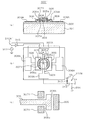
次に、添付図面を参照して本発明の第1実施形態について詳細に説明する。図1は、本発明に係る第1実施形態のマイクロメカニカル静電振動子100の構造を回路構成とともに示す概略平面図(a)及び縦断面図(b)である。
[First Embodiment]
Next, a first embodiment of the present invention will be described in detail with reference to the accompanying drawings. FIG. 1 is a schematic plan view (a) and a longitudinal sectional view (b) showing a structure of a micromechanical
このマイクロメカニカル静電振動子100においては、シリコン基板などで構成される基板101の表面上に、振動子構造体を絶縁するために必要に応じて絶縁膜102が形成されている。この基板101又は絶縁膜102上には、出力電極103、支持部104及び振動体105が構成されている。また、振動体105の両側(図示例では図1(a)の上下両側、図1(b)の前後両側)には、振動体105の外周部に空隙106を介して対向配置される、一対の加振電極107,107が形成されている。
In the micromechanical
また、このマイクロメカニカル静電振動子100には、上記一対の加振電極107,107に同相の交流電力を印加するための給電手段を構成する給電回路110が設けられている。この給電回路110には、交流電源111と、この交流電源111と加振電極107とを接続する給電線112とが設けられている。この給電回路110は基板101の内部にモノリシックに構成されていることが好ましいが、基板101とは別に構成されていてもよく、或いは、外部から交流電力を供給するための配線構造のみで構成されていてもよい。
Further, the micromechanical
さらに、本実施形態には、出力電極103とともに振動体105の伸縮振動に応じた出力信号を出力するための検出手段を構成する出力回路120が設けられている。この出力回路120においては、電源電位123と出力電極103の出力線121の出力電位との間に接続されたインダクタンス122と、上記出力電位と接地電位との間に接続された負荷抵抗125とが存在し、その先に出力端子126が設けられ、出力電極103と負荷抵抗125及び出力端子126との間にキャパシタンス124が介在している。
Furthermore, in this embodiment, an
本実施形態では、振動体105は、その平面形状が一対の加振電極107,107の間で平面的に伸縮する態様の振動を生じ、この伸縮振動に応じて空隙106が変化することによって、振動体105と加振電極107との間の静電容量が増減する。この静電容量の増減は、出力回路120に生ずる出力電流Ioとして現れるので、この出力電流Ioと付加抵抗125に応じた出力電位Voが出力端子126に出力される。この出力電位Voは、振動体105の固有振動周波数に対応する振動波形を備えたものとなる。
In the present embodiment, the vibrating
振動体105の伸縮振動は、板状の振動体105の平面形状の輪郭(外周部)の形状変化を伴う径方向の振動であり、振動体105と加振電極107,107との間の静電力に起因するものである。この振動モードにおいて、振動体105は、その平面形状、厚み、及び、構成素材の密度や弾性特性(例えば、ヤング率やポアソン比など)によって定まる固有振動周波数を有する。
The expansion and contraction vibration of the vibrating
振動体105は、基板101上に形成された支持部104により支持され、振動体105が支持部104の周囲に広がる形状に構成されていることにより、伸縮振動時において支持部104の影響が低減され、振動体の平面形状に応じた高い周波数を容易に実現できるように構成されている。
The vibrating
振動体105の平面形状は、図示のようにくびれを備えた曲線状の輪郭形状を備えている。具体的には、図2(a)に示すように、振動体105の輪郭は、円弧状に構成された複数(図示例では2つ)の円弧部105a,105bと、これらの円弧部間に両端が滑らかに連結された複数(図示例では2つ)のくびれ部105c,105dとからなるものである。図示例の場合、円弧部105aと105bとは対称形状であり、くびれ部105cと105dとは対称形状である。
The planar shape of the vibrating
そして、図1に実線で示す加振電極107,107は、上記振動体105のくびれ部105c、105dに対してそれぞれ対向配置されている。ただし、電極構造としては、図1に一点鎖線で示すように、くびれ部105c,105dを中心としてその両側の円弧部105a,105bにも対向するように配置された加振電極107′,107′であってもよく、また、図1に2点鎖線で示すように、円弧部105a,105bの中央部分に対向配置される加振電極107″,107″であっても構わない。
The
ここで、図2(a)に2点鎖線で示すように、円弧部105a,105b間の幅とくびれ部105c,105d間の幅とが逆相で伸縮する振動モードで、本実施形態に基づく実施例と図2(c)に示す円盤形状の振動体を用いた比較例とを比較した。ここで、比較例では、本実施形態の円弧部105a,105b間の幅と等しい直径rを有する円盤状の振動体を用い、振動体の厚みt、給電手段に接続された電極構造は同一とした。ちなみに、実施例及び比較例のいずれにおいても、振動体の厚みはt=1μm、上記直径r=10μm、振動体の構成素材はポリシリコンである。また、双方とも振動子の中央部に直径1μmの円形状の支持部を設け、固有値解析を実施した。この計算に用いた振動体の材料定数は、ヤング率:160GPa、ポアソン比:0.3、密度:2500kg/m3とした。
この結果、比較例の固有振動周波数は約385MHzであったのに対して、本実施形態の固有振動周波数は約441MHzとなった。また、図2(b)に示すように、本実施形態の振動体105における、円弧部105a,105b間の幅とくびれ部105c,105d間の幅とが同相で伸縮する振動モードの固有振動周波数は983MHzとなった。このように、本実施形態のマイクロメカニカル振動子は、従来構造の比較例に対して高周波化を図ることができることが確認された。
Here, as shown by a two-dot chain line in FIG. 2A, this is a vibration mode in which the width between the
As a result, the natural vibration frequency of the comparative example was about 385 MHz, whereas the natural vibration frequency of the present embodiment was about 441 MHz. In addition, as shown in FIG. 2B, in the vibrating
[第2実施形態]
次に、図3を参照して、本発明に係る第2実施形態のマイクロメカニカル静電振動子200について説明する。この振動子200は、上記第1実施形態の振動体とほぼ同様の平面形状を有する振動体205を有するが、この振動体205は、一対のくびれ部の中央部が梁状の支持部204に接続されることによって支持されている点で上記第1実施形態とは異なる。この支持部204は、振動体205を両側から梁状に支持し、ほぼ水平に(すなわち基板201の表面と平行に)伸びるように構成されている。また、支持部204の反対側は出力電極203に接続されている。
[Second Embodiment]
Next, a micromechanical
また、本実施形態では、振動体205の円弧部の中央部分に対して一対の加振電極207,207がそれぞれ対向配置されている。そして、これらの加振電極207,207には同相の交流電力が給電回路210の交流電源211及び給電線212により印加される。また、出力電極203には、出力回路220が接続されている。出力回路220には、第1実施形態と同様の、出力線221、インダクタンス222、電源電位223、キャパシタンス224、負荷抵抗225、出力端子226が設けられる。
In the present embodiment, a pair of
この実施形態においても、先の第1実施形態と同様に振動体205の高周波化を図ることができる。また、振動体205と支持部204とを同じ層で同じ高さを有するものとして構成することができるため、第1実施形態よりも成膜プロセスに余裕が生じ、迅速にかつ高い再現性をもって振動体を形成することが可能になる。
Also in this embodiment, it is possible to increase the frequency of the vibrating
[その他の実施形態]
図4は、上記振動体の代わりに用いることのできる異なる平面形状を有する振動体の平面図である。図4(a)に示す振動体2305の平面形状は、中心の周りに3つの円弧部2305a,2305b,2305cが設けられ、これらの円弧部間にそれぞれくびれ部2305d,2305e,2305fが連結された輪郭を有する。また、図4(b)に示す振動体2405の平面形状は、4つの円弧部2405a,2405b,2405c,2405dが設けられ、これらの円弧部間にそれぞれくびれ部2405e,2405f,2405g,2405hが連結された輪郭を有する。
[Other Embodiments]
FIG. 4 is a plan view of a vibrating body having a different planar shape that can be used in place of the vibrating body. The planar shape of the vibrating
[製造方法]
図5及び図6には、上記第1実施形態のマイクロメカニカル静電振動子100を製造するプロセス例を示す工程断面図を示す。このプロセスでは、最初に、図5(a)に示すように、シリコン基板などで構成される基板101上にSiO2で構成される絶縁層102Aと、Si3N4で構成される絶縁層102Bとを形成する。絶縁層102Aは熱酸化法などで形成でき、また、絶縁層102BはプラズマCVD法などで形成できる。絶縁層102Aと絶縁層102Bは、上記の絶縁膜102を構成する。
[Production method]
5 and 6 are process cross-sectional views illustrating a process example for manufacturing the micromechanical
次に、図5(b)に示すように、フォトリソグラフィ法などを用いて絶縁層102A,102Bに開口102xを形成し、その上に、図5(c)に示すように蒸着法やスパッタリング法などを用いてアルミニウムなどの金属などからなる導電層103pを形成する。
そして、フォトリソグラフィ法などでパターニングを行うことにより、図5(d)に示すように、出力電極103と、入力電極107pを形成する。
Next, as shown in FIG. 5B,
Then, an
その後、図5(e)に示すようにPSG(リンドープガラス)膜などからなる犠牲層108をCVD法などで形成し、さらに図5(f)に示すように開口108xを形成する。
その後、図6(g)に示すように、ポリシリコンなどで導電層105Sを成膜する。このとき、開口108x内には支持部104が同時に形成される。さらに、図6(h)に示すように、レジストなどでマスク109を形成し、このマスク109を介して導電層105Sをパターニングすることで、図6(i)に示すように、振動体105、空隙106、及び、電極107を形成する。
Thereafter, a
Thereafter, as shown in FIG. 6G, a
最後に、図6(j)に示すように、犠牲層108をエッチングなどで除去することにより、図1に示す振動子構造体が完成する。ここで、加振電極107は図示しない支持層(上記犠牲層などで構成される。)上に支持された状態となっており、また、加振電極107は図示しないコンタクトホールなどを介して基板上の入力電極107pに導電接続される。
Finally, as shown in FIG. 6J, the
上記のように、本発明は、振動体の平面形状の輪郭にくびれを設けることにより、高周波化が可能になるとともに、このくびれによって振動体の伸縮振動モード(その輪郭が変動する態様の振動モード)の制御が容易になり、より安定した伸縮振動を発生させることが可能になる。例えば、くびれ部を設けることによって複数の固有振動周波数をもつことになるため、電極構造や印加周波数などによって一つの振動体を異なる振動周波数で使い分けることも可能になる。また、第1実施形態の加振電極107と107″のように異なる方位において振動体に対向配置される複数組の加振電極を設けておき、必要な周波数特性に応じて加振電極の組を使い分けることも可能である。
As described above, according to the present invention, it is possible to increase the frequency by providing a constriction in the contour of the planar shape of the vibration body, and the vibration mode of the vibration body (vibration mode in which the contour fluctuates due to the constriction). ) Can be easily controlled, and more stable stretching vibration can be generated. For example, by providing the constricted portion, it has a plurality of natural vibration frequencies, so that it is possible to use one vibration body at different vibration frequencies depending on the electrode structure, the applied frequency, and the like. Further, a plurality of sets of excitation electrodes arranged opposite to the vibrating body in different directions, such as the
本実施形態では、振動体は、その両側に配置される一対の加振電極に対して対称な平面形状となり得るものであることが安定した振動を発生させることができる点で好ましい。
ここで、一対の加振電極に対して対称な形状とは、例えば、一対の加振電極の中心部を結ぶ線分の垂直二等分線を対称軸としたときの線対称形状であることを意味する。この場合にはさらに、一対の電極の中心部を結ぶ線分を対称軸とした線対称形状でもあることが望ましい。例えば、上記第1及び第2実施形態の振動体105,205や図4(b)に示す振動体405は、このような高い対称性を実現しうる形状である。
In the present embodiment, it is preferable that the vibrating body can have a plane shape that is symmetric with respect to the pair of excitation electrodes arranged on both sides of the vibrating body in that stable vibration can be generated.
Here, the shape symmetric with respect to the pair of excitation electrodes is, for example, a line symmetry shape with a perpendicular bisector connecting the center portions of the pair of excitation electrodes as a symmetry axis. Means. In this case, it is also desirable that the line segment connecting the center portions of the pair of electrodes has a line symmetrical shape with the axis of symmetry as the axis of symmetry. For example, the vibrating
尚、本発明のマイクロメカニカル静電振動子は、上述の図示例にのみ限定されるものではなく、本発明の要旨を逸脱しない範囲内において種々変更を加え得ることは勿論である。例えば、上記実施形態のマイクロメカニカル静電振動子は、入力回路と出力回路とを別々に有するものとして構成されているが、振動子の利用態様に応じて、入力回路と出力回路とを共通の回路構造で実現するなど、種々の構成を採用することができる。 Note that the micromechanical electrostatic vibrator of the present invention is not limited to the illustrated examples described above, and it is needless to say that various modifications can be made without departing from the gist of the present invention. For example, the micromechanical electrostatic vibrator of the above embodiment is configured to have an input circuit and an output circuit separately, but the input circuit and the output circuit are shared depending on the usage mode of the vibrator. Various configurations such as realization with a circuit structure can be employed.
[第3実施形態]
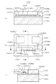
図7は、本発明に係る第3実施形態のマイクロメカニカル静電振動子300の構造を示す概略縦断面図(a)、概略平面図(b)及び振動体305の形状を示す拡大斜視図(c)である。この静電振動子300は、基板301上に絶縁層302を形成し、この絶縁層302上に、振動子構造体を形成したものである。基板301としては、シリコン単結晶、GaAsやInP等の化合物半導体などの半導体基板であることが好ましいが、ガラス、石英、セラミックス、合成樹脂などの他の素材で構成されたものであっても構わない。
また、絶縁層302は、基板301が絶縁体である場合には不要であるが、基板301が半導体や導体である場合、或いは、基板301は絶縁体であるがその表面上に導体パターンなどの導電体が存在している場合には必要となる。
[Third Embodiment]
FIG. 7: is a schematic longitudinal cross-sectional view (a) which shows the structure of the micro mechanical
The insulating
振動子構造体は、基準電極303上に配置された支持体304を介して支持部305aが支持されてなる振動体305と、この振動体305の外縁305bに対向する加振電極306とを有する。基準電極303、支持体304及び振動体305は相互に導電接続されている。これらは或る程度の導電性を有する素材、例えばポリシリコンなどで構成される。振動体305は中央部を支持体304により支持された支持部305aとする板状体として構成されている。図示例では、振動体305は円盤状に形成されている。
The vibrator structure includes a vibrating
この振動体305の両側(図示左右側)には一対の加振電極306,306が配置されている。加振電極306は、振動体305の外縁305bに沿って伸びる電極面306aを有する。図示例では振動体305の外縁305bは円弧状に伸びた円筒凸面となっているので、加振電極306の電極面306aは、外縁305bの面形状に対応する面形状、すなわち円弧状に伸びた円筒凹面になっている。このように、振動体305の外縁305bと、加振電極306の電極面306aとの間には、両者の対向部の全体に亘って一定の間隔が存するように構成されている。
A pair of
図示例の場合、基準電極303には接続端子(ボンディングパッド)303Aが導電接続され、加振電極306には接続端子(ボンディングパッド)306Aが導電接続されている。ただし、これらの接続端子303A,306Aを設けずに、例えば、基準電極303及び加振電極306を基板301に形成した回路内に導電接続しても構わない。
In the illustrated example, a connection terminal (bonding pad) 303A is conductively connected to the
本実施形態では、図7(b)に示すように、加振電極306に入力回路310Aが導電接続され、基準電極303に出力回路310Bが導電接続されている。入力回路310Aは加振電極306に駆動電圧を供給するものであり、例えば、交流電源311が設けられる。また、出力回路310Bは基準電極303の電位に基づいて出力電圧を出力するものであり、例えば、基準電極303とバイアス電位Vbとの間に接続されたインダクタンス312と、基準電極303と出力電位Voとの間に接続されたキャパシタンス313と、出力電位Voと接地電位との間に接続された抵抗314とを備えている。バイアス電圧Vbは基準電極303にバイアス電圧を印加するためのものである。ここで、出力電位Voはキャパシタンス313の充放電電流と抵抗314とによって得られた、基準電極303の電位変動に相当する電位変化を示す。
In this embodiment, as shown in FIG. 7B, the
本実施形態では、上記入力回路310Aに相当する部分から供給される入力信号を、振動体305と加振電極306の振動特性によって変調し、出力電位Voを得ることのできる高周波フィルタとして動作する。そのフィルタ特性は、振動体305の伸縮振動モードの特性に依存することになる。具体的には、入力信号によって振動体305と加振電極306との間に静電力が発生し、この静電力の変化(向きの交代)によって振動体305が伸縮振動する。振動体305が振動すると、振動体305と加振電極306との間の距離が変動するため、両者間の静電容量も変動し、この静電容量の変動に応じて出力電位Voも周期的に変化する。
In the present embodiment, an input signal supplied from a portion corresponding to the
振動体305は、図7(c)に示すように、支持体304によって支持される支持部305aから外縁305bに向けて厚さが増大する形状を有している。具体的には、図示例の場合、支持部305aから半径方向外側に向けて所定範囲に亘って厚さの等しい部分があり、その外側に段差面305cが設けられ、この段差面305cよりも半径方向外側にある部分の厚さは、段差面305cよりも半径方向内側にある部分よりも大きくなっている。図示例の場合、段差面305cは振動体305の表面側と裏面側の双方に設けられている。また、段差面305cは外縁305bとは反対側、すなわち、中心側を向いた面となっている。
As shown in FIG. 7C, the vibrating
振動体305は、加振電極306によって板状体の主面(図示水平面)を振動面として伸縮変形し、伸縮モードの振動を行う。ここで、振動体305の上記厚さは振動面と直交する方向の幅である。振動体305はその厚さ方向に対称な形状(すなわち表裏対称形状)を有する。これによって、振動面上の振動状態を安定させ、振動面上にない副次的な振動モードの発生を抑制することができるため、振動エネルギーの無駄な散逸を防止することができる。
The vibrating
加振電極306に電力が供給されると、振動体305の外縁305bと加振電極306との間に静電力が発生し、加振電極306に印加される電圧が交流電圧(交代電圧)であれば、振動体305の外縁305bと加振電極306との間に静電斥力と静電引力とが交互に及ぼされる。これによって、振動体305は一対の加振電極306の間において周期的に収縮と伸長を繰り返すことになり、伸縮モードの振動が励起される。
When power is supplied to the
このとき、加振電極306に印加される入力電圧の周波数が振動体305の伸縮モードの固有周波数と一致すれば、振動体305は共振し、その出力信号は大きくなる。したがって、本実施形態の静電振動子300はバンドパスフィルタや発振器として用いることができる。ここで、振動体305の直径が1〜100μm程度、厚さが0.1〜10μm程度であるとき、振動体305に励起された伸縮振動の固有周波数は10MHz〜1GHz程度となる。
At this time, if the frequency of the input voltage applied to the
本実施形態では、振動体305は、その支持部305aから外縁305bに向けて厚さが増大する形状となっているため、外縁305bと加振電極306との対向面積を増加させることができることから振動体305が受ける静電力が大きくなるとともに、振動体305の重量分布が外縁305b寄りに偏ったものとなるので、振動体305の伸縮振動に対する実効的な弾性率を高めることができる。したがって、振動体305の伸縮変位量を増加させることができることになるため、入力電圧に対する出力電圧の比を従来よりも高めることができる。
In the present embodiment, since the vibrating
本実施形態の静電振動子300は、絶縁層302と振動体305及び加振電極306との間にSiO2、PSG(リンドープガラス)、有機樹脂などで構成される犠牲層を形成し、振動体305及び加振電極306を形成してから犠牲層をエッチングなどで取り除くことによって容易に形成できる。振動体305及び加振電極306はアルミニウムや銅などの金属のほか、ポリシリコンなどの半導体でも形成することができる。いずれの場合でも、蒸着法、スパッタリング法、CVD法などの成膜技術と、フォトリソグラフィなどのパターニング技術とによって上記構造を形成することができる。
In the
[第4実施形態]
次に、図8を参照して、本発明に係る第4実施形態の静電振動子300′について説明する。この実施形態において、上記第3実施形態と同一部分には同一符号を付し、それらの説明は省略する。
[Fourth Embodiment]
Next, an
この実施形態は、基本的に上記第3実施形態に設けられている要素の全てを含んでいるが、振動体305の段差面305cに対向配置される第2の加振電極307X,307Yがさらに設けられている点で、上記第3実施形態と異なる。ここで、第2の加振電極307Xは振動体305の裏面(下面)上に設けられた段差面305cに対向配置され、その段差面305c側にある加振電極306の電極面306aに向いている。第2の加振電極307Yは振動体305の表面(上面)上に設けられた段差面305cに対向配置され、その段差面305c側にある加振電極306の電極面306aに向いている。ここで、第2の加振電極307X,307Yのうちいずれか一方のみを設けても構わない。
Although this embodiment basically includes all the elements provided in the third embodiment, the
第2の加振電極307X,307Yは、共通の接続端子(ボンディングパッド)307Aに導電接続されている。図8(b)に示すように、第2の加振電極307X,307Yには、入力回路310A′に設けられた反転回路315から、上記加振電極306とは逆相の交流電圧(交代電圧)が供給される。これによって、図8(c)に示すように、振動体305の外縁305bと加振電極306との間に静電斥力が発生しているときには、振動体305の段差面305cと第2の加振電極307X,307Yとの間に静電引力が発生し、振動体305の外縁305bと加振電極306との間に静電引力が発生しているときには、振動体305の段差面305cと第2の加振電極307X,307Yとの間に静電斥力が発生するというように駆動することができる。これによって、振動体305の伸縮振動を発生させるための静電力が増加するので、振動体305の伸縮変位量を増加させることができ、その結果、出力電圧(出力信号の振幅)を高めることができ、入力電圧に対する出力電圧の比を従来よりもさらに高めることができる。
The
この実施形態では、第2の加振電極307X,307Yを形成するために、第2の加振電極307Xと振動体305との間、及び、振動体305と第2の加振電極307Yとの間にそれぞれ犠牲層を介在させ、最後に犠牲層をエッチングなどにより取り除くことによって第3実施形態と同様に製造することができる。
In this embodiment, in order to form the
[実施例と比較例との対比]
次に、上記第3実施形態の実施例と、第3実施形態の振動体305に代えて支持部305aから外縁305bまで同一の厚さを有する平行板状の振動体を用いた比較例とを対比した結果について説明する。なお、実施例と比較例とは、振動体の重量及び平均厚さが同一である。したがって、実施例の振動体は、比較例の中央側の部分の肉を一定量取り去り、その一定量の肉を外縁側に付加した形状となっている。
[Contrast between Example and Comparative Example]
Next, an example of the third embodiment and a comparative example using a parallel plate-like vibrating body having the same thickness from the
円盤型振動子の共振周波数fは、f=(α/R)(E/ρ)1/2で表される。ここで、αは振動体のポアソン比と振動モードに依存する係数、Rは振動体の直径、Eは振動体のヤング率、ρは振動体の密度である。この式から、共振周波数は直径Rに反比例することがわかる。 The resonance frequency f of the disk-type vibrator is represented by f = (α / R) (E / ρ) 1/2 . Here, α is a coefficient depending on the Poisson's ratio and vibration mode of the vibrating body, R is the diameter of the vibrating body, E is the Young's modulus of the vibrating body, and ρ is the density of the vibrating body. From this equation, it can be seen that the resonance frequency is inversely proportional to the diameter R.
図9は、実施例と比較例における振動体の直径と固有周波数との関係を示すグラフである。実施例と比較例のいずれも上記の式を反映し、振動数が直径に反比例する態様となっている。また、実施例は比較例に対して共振周波数がやや低くなっているが、実施例においても、基本的には数百MHzという高い周波数で振動することがわかる。ここで、振動体の材料はSiであり、ヤング率160Gpa、密度2500kg/m3としてある。 FIG. 9 is a graph showing the relationship between the diameter of the vibrating body and the natural frequency in the example and the comparative example. Each of the example and the comparative example reflects the above formula, and the frequency is inversely proportional to the diameter. In addition, although the resonance frequency of the example is slightly lower than that of the comparative example, it can be seen that the example also basically vibrates at a high frequency of several hundred MHz. Here, the material of the vibrating body is Si, and the Young's modulus is 160 Gpa and the density is 2500 kg / m 3 .
図10は、比較例の振動体における直径及び厚さと固有周波数との関係を示すグラフである。この図にてわかるように、円盤型振動子では、直径を小さくすれば固有周波数が高くなるが、厚さが変化しても固有周波数の変化はきわめて少ない。ところが、円盤型振動子の場合、伸縮モードで振動させるため、直径が小さくなると伸縮変位量がさらに小さくなり、入力電圧に対する出力電圧の比がさらに低下する。したがって、実施例の構造を用いて伸縮変位量を高めることにより、振動体の直径を小さくした場合でも、入力電圧に対する出力電圧の比を大きくすることができるという利点があることが理解できる。 FIG. 10 is a graph showing the relationship between the natural frequency and the diameter and thickness of the vibrator of the comparative example. As can be seen from this figure, in the disk-type vibrator, the natural frequency increases as the diameter decreases, but the natural frequency changes very little even if the thickness changes. However, in the case of a disk-type vibrator, since it vibrates in an expansion / contraction mode, the amount of expansion / contraction displacement is further reduced when the diameter is reduced, and the ratio of the output voltage to the input voltage is further reduced. Therefore, it can be understood that there is an advantage that the ratio of the output voltage to the input voltage can be increased by increasing the expansion / contraction displacement amount using the structure of the embodiment, even when the diameter of the vibrating body is reduced.
図11は、振動体を片持ち梁形状として屈曲モードで振動させた場合の、片持ち梁の支持部より先の長さと、固有周波数との関係を示すグラフである。屈曲モードの振動体では振動の変位量を大きく採ることができるが、図示のように、固有周波数は数MHz程度であり、高周波化に適しないことがわかる。 FIG. 11 is a graph showing the relationship between the natural frequency and the length beyond the cantilever beam support when the vibrating body is cantilever-shaped and vibrated in the bending mode. A bending mode vibrating body can take a large amount of vibration displacement. However, as shown in the figure, the natural frequency is about several MHz, which is not suitable for high frequency.
次に、実施例と比較例の伸縮振動時における変位量を比較した。その結果を図16及び図17に示す。図16は実施例の変位量の分布を等変位量線で示し、図17は比較例の変位量の分布を等変位量線で示したものである。ここで、振動子の材料はSiであり、ヤング率170GPa、密度2500kg/m3とした。実施例と比較例の質量は同一で、同一荷重を与えて振動させるものとし、さらに同一モードで振動していると仮定し、変位量分布を求めた。図示のように、図17に示す実施例の方が図16に示す比較例に較べて変位量が大きくなっている。また、各振動子のばね定数を求めると、実施例では643N/m、比較例では1103N/mとなった。実施例でばね定数が低下することは、周波数が低下することも意味するが、同じ荷重を与えた場合には変位量(振幅)が大きくなることを意味する。ここで、実施例と比較例に同一の入力電圧を加えると、実施例の外縁305bの面積は比較例よりも大きいため、実施例の受ける応力(静電力)は比較例よりも大きくなるから、上記の図16と図17に示す場合よりも変位量の差はさらに大きくなるものと考えられる。
Next, the displacement amount at the time of stretching vibration of the example and the comparative example was compared. The results are shown in FIGS. FIG. 16 shows the displacement distribution of the example with an equal displacement curve, and FIG. 17 shows the displacement distribution of the comparative example with an equal displacement curve. Here, the material of the vibrator was Si, the Young's modulus was 170 GPa, and the density was 2500 kg / m 3 . The masses of the example and the comparative example are the same, and the same load is applied to vibrate, and further, the displacement distribution is obtained assuming that the vibration is performed in the same mode. As shown in the figure, the displacement amount in the embodiment shown in FIG. 17 is larger than that in the comparative example shown in FIG. Further, the spring constant of each vibrator was found to be 643 N / m in the example and 1103 N / m in the comparative example. Decreasing the spring constant in the embodiment also means that the frequency decreases, but the displacement (amplitude) increases when the same load is applied. Here, when the same input voltage is applied to the example and the comparative example, since the area of the
[その他の実施形態]
図12は、上記とは異なる振動体405の形状を示す概略斜視図である。この振動体405は上記第3及び第4実施形態の振動体の代わりに用いることができるものである。振動体405は、中心の支持部405aから外縁405bまでの間の複数箇所(図示例では2箇所)に段差面405c、405dが設けられている。このようにすると、重量分布はさらに外縁405b側に偏ることになるため、振動時の変位量をさらに高めることができる。
[Other Embodiments]
FIG. 12 is a schematic perspective view showing a shape of a vibrating
図13は、さらに異なる振動体505の概略縦断面図である。この振動体505も上記第3及び第4実施形態の振動体の代わりに用いることができる。この振動体505では、支持体504によって支持される中央の支持部505aから外縁505bに向けて厚さが徐々に大きくなっている。このようにしても、外縁505b側に重量分布が偏ることになるとともに、外縁505bの面積を増大させることができるので、振動時の変位量をさらに高めることができる。
FIG. 13 is a schematic longitudinal sectional view of a further
図14は、別の振動体605の概略斜視図である。この振動体605もまた上記第3及び第4実施形態の振動体の代わりに用いることができる。この振動体605では、支持体604によって支持される支持部605aと、外縁605bとの間が2本の梁部605sによってのみ接続されている点で上記の振動体と異なる。この場合には、中心側の所定の半径位置における厚さの平均値よりも外縁側の所定の半径位置における厚さの平均値が大きくなっている。2本の梁部605sは支持部605aから相互に反対側に伸び、リング状の外縁605bに接続されている。
FIG. 14 is a schematic perspective view of another vibrating
図15は、さらに別の振動体705の概略斜視図である。この振動体705もまた上記第3及び第4実施形態の振動体の代わりに用いることができる。この振動体705では、支持体704によって支持される支持部705aと外縁705bとの間が4つの梁部705sによって接続されている。このように、支持部と外縁とを接続する梁部は何本であっても構わない。この場合にも、中心側の所定の半径位置における厚さの平均値よりも外縁側の所定の半径位置における厚さの平均値が大きくなっている。
FIG. 15 is a schematic perspective view of still another vibrating
尚、本発明のマイクロメカニカル静電振動子は、上述の図示例にのみ限定されるものではなく、本発明の要旨を逸脱しない範囲内において種々変更を加え得ることは勿論である。例えば、上記第3及び第4実施形態では、振動体の平面形状を円形としたが、本発明はこのような平面形状に限られず、円形以外の種々の平面形状(楕円、長円、矩形など)であっても構わない。また、上記第3及び第4実施形態では、振動体の中心が支持部となっているが、伸縮モードで振動するのであれば、振動体が片持ち支持されるなど、支持部が振動体の中心ではなく偏った位置にあっても構わない。 Note that the micromechanical electrostatic vibrator of the present invention is not limited to the illustrated examples described above, and it is needless to say that various modifications can be made without departing from the gist of the present invention. For example, in the third and fourth embodiments, the planar shape of the vibrating body is circular, but the present invention is not limited to such a planar shape, and various planar shapes other than circular (an ellipse, an ellipse, a rectangle, etc.) ). Further, in the third and fourth embodiments, the center of the vibrating body is the support portion. However, if the vibrating body vibrates in the expansion / contraction mode, the supporting portion of the vibrating body is supported, for example, the vibrating body is cantilevered. It does not matter if it is not at the center but at a biased position.
[第5実施形態]
図18は、本発明に係る第5実施形態のマイクロメカニカル静電振動子800の構造を示す概略縦断面図(a)及び概略平面図(b)である。このマイクロメカニカル静電振動子800は、基板801上に絶縁層802を形成し、この絶縁層802上に、振動子構造体を形成したものである。基板801としては、シリコン単結晶、GaAsやInP等の化合物半導体などの半導体基板であることが好ましいが、ガラス、石英、セラミックス、合成樹脂などの他の素材で構成されたものであっても構わない。また、絶縁層802は、基板801が絶縁体である場合には不要であるが、基板801が半導体や導体である場合、或いは、基板801は絶縁体であるがその表面上に導体パターンなどの導電体が存在している場合には必要となる。
[Fifth Embodiment]
FIG. 18 is a schematic longitudinal sectional view (a) and a schematic plan view (b) showing the structure of the micromechanical
振動子構造体は、基準電極803上に接続されてなる振動体805と、この振動体805に隣接配置された加振電極806とを有する。基準電極803及び振動体805は相互に導電接続されている。これらは或る程度の導電性を有する素材、例えばポリシリコンなどで構成される。振動体805は、基準電極803に下端が固定された支持部805aと、この支持部805aの上部に接続された従動部805bとを有している。従動部805bは、支持部805aよりも平面的に拡大された範囲に広がる形状を有している。具体的には、従動部805bは支持部805aが中心位置(重心位置でもある。)に接続されてなる板状体として構成されている。従動部805bは支持部805aを中心とする回転方向に見て変化する形状、すなわち、形状変化のない任意の物体を回転させたときの回転軌跡を占有する形状である回転体形状以外の形状を有する。図示例では、従動部805bは楕円盤状に形成されている。この実施形態において、従動部805bは、円柱状に形成された支持部805aの上部に片持ち支持された状態となっている。なお、図示例とは異なるが、従動部805bを上下の支持部によって両持ち状態で支持した構造としてもよい。
The vibrator structure includes a vibrating
この振動体805の両側(図示左右側)には一対の加振電極806,806が配置されている。加振電極806は、振動体805の外縁805cに沿って伸びる電極面806aを有する。図示例では振動体805の外縁805cは楕円弧状に伸びた楕円筒凸面となっているので、加振電極806の電極面806aは、外縁805cの面形状に対応する面形状、すなわち楕円弧状に伸びた楕円筒凹面になっている。加振電極806の電極面806aは、振動体805の外縁805cのうち、支持部805aの軸線を中心とする回転方向の成分を有する方向を向いた表面部分に対向している。すなわち、加振電極806は、振動体805に対してそれぞれ偏心した位置(長軸及び短軸から回転方向にずれた位置)において対向配置されている。
A pair of
図示例の場合、基準電極803には接続端子(ボンディングパッド)803Aが導電接続され、加振電極806には接続端子(ボンディングパッド)806Aが導電接続されている。ただし、これらの接続端子803A,806Aを設けずに、例えば、基準電極803及び加振電極806を基板801に形成した回路内に導電接続しても構わない。
In the illustrated example, a connection terminal (bonding pad) 803A is conductively connected to the
本実施形態では、図18(b)に示すように、加振電極806に入力回路810Aが導電接続され、基準電極803に出力回路810Bが導電接続されている。入力回路810Aは加振電極806に駆動電圧を供給するものであり、例えば、交流電源811が設けられる。また、出力回路810Bは基準電極803の電位に基づいて出力電圧を出力するものであり、例えば、基準電極803とバイアス電位Vbとの間に接続されたインダクタンス812と、基準電極803と出力電位Voとの間に接続されたキャパシタンス813と、出力電位Voと接地電位との間に接続された抵抗814とを備えている。バイアス電圧Vbは基準電極803にバイアス電圧を印加するためのものである。ここで、出力電位Voはキャパシタンス813の充放電電流と抵抗814とによって得られた、基準電極803の電位変動に相当する電位変化を示す。
In this embodiment, as shown in FIG. 18B, the
本実施形態では、上記入力回路810Aに相当する部分から供給される入力信号を、振動体805と加振電極806の振動特性によって変調し、出力電位Voを得ることのできる高周波フィルタとして動作する。そのフィルタ特性は、振動体805の捩れ振動モードの特性に依存することになる。具体的には、入力信号によって振動体805と加振電極806との間に静電力が発生し、この静電力の変化(向きの交代)によって振動体805が捩れ振動する。振動体805が振動すると、振動体805と加振電極806との間の距離が変動するため、両者間の静電容量も変動し、この静電容量の変動に応じて出力電位Voも周期的に変化する。
In the present embodiment, the input signal supplied from the portion corresponding to the
図19は、振動体805の振動態様を示す説明図(a)及び(b)である。図19(a)に示すように、従動部805bと加振電極806との間に静電斥力が発生するときには、振動体805は図示反時計回りに回転させようとする回転トルクを受けることになり、その弾性特性に応じた捩れ変位が発生する。次に、従動部805bと加振電極806との間に静電引力が発生するときには、振動体805は図示時計回りに回転させようとする回転トルクを受けることになり、その弾性特性に応じた捩れ変位が発生する。したがって、従動部805と加振電極806との間に静電斥力と静電引力とを交互に発生させることによって振動体805は捩れ振動する。
FIGS. 19A and 19B are explanatory diagrams (a) and (b) illustrating a vibration mode of the vibrating
なお、振動体805に捩れ振動を生じさせる方法としては、上記のように静電斥力と静電引力とを交互に印加する方法に限らず、静電斥力と静電引力のいずれか一方を周期的に印加する方法であっても構わない。また、実施形態では、振動体805に対して一対の加振電極806が設けられているが、一つの加振電極だけを設けてもよく、或いは、3以上の加振電極806を設けてもよい。
Note that the method of generating torsional vibration in the vibrating
上記のように振動体805が振動するとき、加振電極806に印加される入力電圧の周波数が振動体805の捩れモードの固有周波数と一致すれば、振動体805は共振し、その出力信号は大きくなる。したがって、本実施形態のマイクロメカニカル静電振動子800はバンドパスフィルタや共振器として用いることができる。ここで、例えば、振動体805の上部の長径が10μm、短径が5μm、厚さが2μmであり、支持部805aの直径が2μm、長さが5μm、振動体105の構成材料がポリシリコンであるとき、振動体805の捩れ振動の固有周波数は約15〜20MHz程度となる。
When the vibrating
本実施形態では、振動体805の捩れ振動を用いているため、屈曲振動を用いる場合よりも高い周波数で振動させることができるとともに、伸縮振動(縦振動)を用いる場合よりも大きな変位量を得ることができることから、入力電圧に対する出力電圧の比を従来よりも高めることができ、入力電圧(駆動電圧)の低電圧化を図ることができる。特に、振動体805が支持部805aと、この支持部805aに接続された拡大された従動部805bとによって構成されているので、静電力により受ける回転トルクが大きくなり、効率的に捩れ振動を生じさせることができるとともに、捩れ振動の変位量を大きくすることができるので、入力電圧に対する出力電圧の比を大きくすることができる。
In the present embodiment, since the torsional vibration of the vibrating
本実施形態では、支持部805aが従動部805bの重心位置に接続されているので、従動部805bの支持部805aによる支持状態が安定しているため、駆動電極806から静電力を受けたときでも、捩れ方向以外の振動が生じにくいことから、安定した姿勢で捩れ振動することができ、振動エネルギーのロスも少ない。
In this embodiment, since the
本実施形態の静電振動子800は、絶縁層802と振動体805及び加振電極806との間にSiO2、PSG(リンドープガラス)、有機樹脂などで構成される犠牲層を形成し、振動体805及び加振電極806を形成してから犠牲層をエッチングなどで取り除くことによって容易に形成できる。振動体805及び加振電極806はアルミニウムや銅などの金属のほか、ポリシリコンで形成することもできる。特に、振動体805及び加振電極806をポリシリコンで構成する場合には、シリコン半導体プロセスをそのまま適用することができ、特にシリコン基板上に形成する場合にきわめて容易に製造することができる。いずれの場合でも、蒸着法、スパッタリング法、CVD法などの成膜技術と、フォトリソグラフィなどのパターニング技術とによって上記構造を形成することができる。
In the
[第6実施形態]
次に、図20を参照して、本発明に係る第6実施形態の静電振動子900について説明する。この実施形態において、振動体905及び駆動電極906以外の構成は、上記第5実施形態と同一に構成することができるため、それらの説明は省略する。
[Sixth Embodiment]
Next, an
この実施形態において、振動体905は、下端が固定された支持部905aと、この支持部905aの上端に接続された従動部905bとを有する。従動部905bは、支持部905aに対する接続部分から周囲に放射状に伸びる複数の輻状部905sと、これらの輻状部905sの先端に接続された環状の外輪部905cとを備えている。図示例では、輻状部905sは90度間隔で4本設けられている。輻状部905sの間は、捩れ振動の振動面と直交する方向に貫通する開口部905tとなっている。
In this embodiment, the vibrating
一方、加振電極906は上記の開口部905tの内部に配置されている。図示例では複数の開口部905tにそれぞれ加振電極906が配置されている。加振電極906は、静電力が印加されていない初期状態においては、開口部905tのうち、軸線周りの回転方向のいずれか一方に偏った位置に配置され、輻状部905sの側面905saに対向配置されている。そして、従動部905bと加振電極906との間に静電斥力が生じるようにすると、加振電極906から輻状部905sが離反する方向に振動体905が回転し、図21(a)に示すように、振動体905は図示反時計回りに捩れる。また、従動部905bと加振電極906との間に静電引力が生じるようにすると、加振電極906に輻状部905sが接近する方向に振動体905が回転し、図21(b)に示すように、振動体905が図示時計回りに捩れる。したがって、振動体905と加振電極906との間に静電斥力と静電引力とを交互に発生させることによって振動体905は捩れ振動する。
On the other hand, the
なお、振動体905に捩れ振動を生じさせる方法としては、上記のように静電斥力と静電引力とを交互に印加する方法に限らず、静電斥力と静電引力のいずれか一方を周期的に印加する方法であっても構わない。また、実施形態では、振動体905に対して4つの加振電極906が設けられているが、加振電極906の数は任意である。さらに、上記実施形態では振動体905の一端(下端)のみを固定しているが、両端支持であっても構わない。
Note that the method of generating torsional vibration in the vibrating
本実施形態でも、支持部905aが従動部905bの重心位置に接続されているので、従動部905bの支持部905aによる支持状態が安定しているため、駆動電極906から静電力を受けたときでも、捩れ方向以外の振動が生じにくいことから、安定した姿勢で捩れ振動することができ、振動エネルギーのロスも少ない。
Also in this embodiment, since the support portion 905a is connected to the position of the center of gravity of the driven
[振動モードと振動子の固有振動数との関係]
次に、上記第5及び第6実施形態の捩れ振動を用いた振動子と、屈曲振動を用いた振動子と、伸縮振動(縦振動)を用いた振動子との関係について説明する。
[Relationship between vibration mode and natural frequency of vibrator]
Next, the relationship between the vibrator using torsional vibration, the vibrator using bending vibration, and the vibrator using stretching vibration (longitudinal vibration) according to the fifth and sixth embodiments will be described.
捩れ振動を用いる振動子の固有振動数fbは、振動体を長さLの棒状体とした場合、
fb=(Bn/2L)(G/ρ)1/2 …(1)
で表される。ここで、Bnは振動体の棒端の条件と、振動次数によって定まる係数であり、両端固定の場合、Bn=n=1,2,3,・・・となり、一端固定、他端自由の場合、Bn=n−1/2=1/2,3/2,5/2,・・・である。また、GはG=E/{2・(1+σ)}(Eはヤング率、σはポアソン比)であり、ρは密度である。
The natural frequency fb of a vibrator that uses torsional vibration is, when the vibrating body is a rod-shaped body having a length L,
fb = (Bn / 2L) (G / ρ) 1/2 (1)
It is represented by Here, Bn is a coefficient determined by the condition of the rod end of the vibrating body and the vibration order. When both ends are fixed, Bn = n = 1, 2, 3,... Bn = n−1 / 2 = 1/2, 3/2, 5/2,. G is G = E / {2 · (1 + σ)} (E is Young's modulus, σ is Poisson's ratio), and ρ is density.
一方、屈曲振動(曲げ振動)を用いる振動子の固有振動数faは、振動体を長さLの棒状体とした場合、
fa=(An/L2)(EI/m)1/2 …(2)
で表される。ここで、Anは振動体の棒端の条件と、振動次数によって定まる係数であり、両端固定の場合、A1=4.730、A2=7.853、A3=10.996,・・・(1−coshA・cosA=0の解)となり、一端固定、他端自由の場合、A1=1.875、A2=4.694、A3=7.855,・・・(1+coshA・cosA=0の解)である。また、Eはヤング率、Iは振動体の断面2次モーメントであり、例えば、断面が円の場合にはI=πd4/64(dは直径)である。mは振動体の断面積Sと密度ρの積である。
On the other hand, the natural frequency fa of the vibrator using bending vibration (bending vibration) is, when the vibrating body is a rod-shaped body having a length L,
fa = (An / L 2 ) (EI / m) 1/2 (2)
It is represented by Here, An is a coefficient determined by the condition of the rod end of the vibrating body and the vibration order. When both ends are fixed, A1 = 4.730, A2 = 7.853, A3 = 10.996,. -CoshA · cosA = 0), and when one end is fixed and the other end is free, A1 = 1.875, A2 = 4.694, A3 = 7.855,... (1 + coshA · cosA = 0 solution) It is. Further, E is Young's modulus, I is a geometrical moment of inertia of the vibrating body, for example, in the case the cross section is circular is I = πd 4/64 (d in diameter). m is the product of the cross-sectional area S and the density ρ of the vibrating body.
さらに、伸縮振動(縦振動)を用いる振動子の固有振動数fsは、振動体を長さLの棒状体とした場合、
fs=(Bn/2L)(E/ρ)1/2 …(3)
で表される。ここで、Bnは振動体の棒端の条件と、振動次数によって定まる係数であり、両端固定の場合、Bn=n=1,2,3,・・・となり、一端固定、他端自由の場合、Bn=n−1/2=1/2,3/2,5/2,・・・である。また、Eはヤング率、ρは密度である。
Furthermore, the natural frequency fs of the vibrator using the stretching vibration (longitudinal vibration) is, when the vibrating body is a rod-shaped body having a length L,
fs = (Bn / 2L) (E / ρ) 1/2 (3)
It is represented by Here, Bn is a coefficient determined by the condition of the rod end of the vibrating body and the vibration order. When both ends are fixed, Bn = n = 1, 2, 3,... Bn = n−1 / 2 = 1/2, 3/2, 5/2,. E is Young's modulus and ρ is density.
捩れ振動と屈曲振動とを比較すると、固有振動数は振動体の長さLの値によって大小関係が変化する。具体的には、L=Lx=(2An/Bn)・(2(1+σ)I/S)1/2(Sは振動体の断面積)を境として捩れ振動と屈曲振動の固有振動数の大小が入れ替わる。すなわち、振動体の長さLがLxよりも長くなると捩れ振動の固有振動数の方が高くなり、振動体の長さLがLxよりも短くなると屈曲振動の固有振動数の方が高くなる。通常の実用範囲においては、長さLと断面積Sとの関係で、捩れ振動の方が屈曲振動よりも固有振動数は高くなる。また、実際には、屈曲振動においてはLを小さくすれば振動数が増大するが、振動変位量は逆に小さくなるため、入力電圧に対する出力電圧の比が小さくなる。 When the torsional vibration and the bending vibration are compared, the magnitude relationship of the natural frequency varies depending on the value of the length L of the vibrating body. Specifically, L = Lx = (2An / Bn) · (2 (1 + σ) I / S) 1/2 (S is the cross-sectional area of the vibrating body), and the natural frequency of torsional vibration and flexural vibration is the magnitude. Will be replaced. That is, when the length L of the vibrating body is longer than Lx, the natural frequency of torsional vibration is higher, and when the length L of the vibrating body is shorter than Lx, the natural frequency of bending vibration is higher. In the normal practical range, due to the relationship between the length L and the cross-sectional area S, the torsional vibration has a higher natural frequency than the bending vibration. Actually, in bending vibration, if L is decreased, the frequency increases. However, since the vibration displacement amount decreases, the ratio of the output voltage to the input voltage decreases.
また、捩れ振動と伸縮振動(縦振動)とを比較すると、両者の固有振動数の比は、[1/{2・(1+σ)}]1/2となり、常に捩れ振動の方が低い固有振動数を有するが、その差は僅かである。一方、捩れ振動では、上記実施形態のように支持部と拡大された従動部とを有する形状などによって振動変位量を大きくとることができるが、伸縮振動では振動変位量は僅かであり、入力電圧に対する出力電圧の比は小さい。 Also, comparing torsional vibration and stretching vibration (longitudinal vibration), the ratio of the natural frequency of both is [1 / {2 · (1 + σ)}] 1/2 , and the torsional vibration is always lower. Number, but the difference is slight. On the other hand, in torsional vibration, the amount of vibration displacement can be increased by the shape having the support portion and the enlarged follower portion as in the above embodiment, but in the case of stretching vibration, the amount of vibration displacement is small, and the input voltage The ratio of output voltage to is small.
以上のように、本実施形態では、捩れ振動モードを用いていることによって、或る程度の高周波化が可能でありながら、振動変位量を大きく確保できるため、入力電圧に対する出力電圧の比を大きくし、入力電圧の低減を図ることができる。 As described above, in the present embodiment, since the torsional vibration mode is used, a large amount of vibration displacement can be ensured while a certain degree of high frequency is possible, so the ratio of the output voltage to the input voltage is increased. In addition, the input voltage can be reduced.
尚、本発明のマイクロメカニカル静電振動子は、上述の図示例にのみ限定されるものではなく、本発明の要旨を逸脱しない範囲内において種々変更を加え得ることは勿論である。例えば、上記第5及び第6実施形態では、振動体を円柱状の支持部の上に板状の静電力を受ける部分が接続されてなる構造としたが、本発明はこのような平面形状に限られず、従動部が支持部よりも拡大された範囲に広がる形状を有するものであればよく、例えば、支持部に接続される部分から半径方向外側に伸びる棒状の従動部を有する構造であっても構わない。また、上記第5及び第6実施形態の振動体では、支持部が従動部の重心位置に接続されているが、支持部を従動部の重心位置からずれた位置に接続させてなるものであっても構わない。さらに、上記第5及び第6実施形態は、基本的には従動部が静電力を受けることにより支持部が捩れ変形するように構成されているが、支持部とともに従動部もまた捩れ変形するように構成されたものであってもよく、或いは、支持部はほとんど変形しないが、従動部が主として捩れ変形するように構成されたものであっても構わない。 Note that the micromechanical electrostatic vibrator of the present invention is not limited to the illustrated examples described above, and it is needless to say that various modifications can be made without departing from the gist of the present invention. For example, in the fifth and sixth embodiments, the vibrating body has a structure in which a portion that receives a plate-like electrostatic force is connected to a cylindrical support portion. However, the present invention has such a planar shape. Any structure may be used as long as the driven portion has a shape that extends in a range expanded from the support portion.For example, the follower portion has a rod-like follower portion that extends radially outward from a portion connected to the support portion. It doesn't matter. In the vibrating bodies of the fifth and sixth embodiments, the support portion is connected to the gravity center position of the driven portion. However, the support portion is connected to a position shifted from the gravity center position of the driven portion. It doesn't matter. Furthermore, although the fifth and sixth embodiments are basically configured such that the support portion is twisted and deformed when the driven portion receives an electrostatic force, the follower portion is also twisted and deformed together with the support portion. Alternatively, the support portion may be hardly deformed, but the driven portion may be mainly twisted and deformed.
[第7実施形態]
図22は、本発明に係る第7実施形態のマイクロメカニカル静電振動子1000のを示す概略縦断面図、すなわち(b)に示すA−A線に沿った断面を示す概略断面図(a)、概略平面図(b)、及び、上記(a)と直交する断面、すなわち(b)のC−C線に沿った断面を示す概略断面図(c)である。
[Seventh Embodiment]
FIG. 22 is a schematic longitudinal sectional view showing a micromechanical
このマイクロメカニカル静電振動子1000の基本構成は、シリコン基板、ガラス基板、石英基板、セラミック基板などで構成される基板1001の上にSiO2、PSG(リンドープガラス)、TiO2、Ta2O5などの金属酸化物、Si3N4などの窒化シリコン、アクリル樹脂などの合成樹脂などで構成される絶縁層1002が形成されている。
絶縁層1002は、基板1001が導電体基板である場合や半導体基板であるときに、基板と、その上層の導電体との間を絶縁するためのものである。
The basic configuration of the micromechanical
The insulating
基板1001としては、シリコン基板であっても、導電体或いは半導体であって、或る程度の導電性を有する場合と、真性半導体のような絶縁性を有する場合とがあるが、前者の場合には特に絶縁層1002が必要となる。また、後者の場合には絶縁層1002は必ずしも必要ない。さらに、基板1001としてはガラス基板、石英基板、セラミック基板などの絶縁体を用いることも可能であり、このような場合でも、絶縁層1002は不要となる。なお、絶縁性を有する基板1001を用いている場合でも、その表面上に配線パターンなどの導電膜が形成されている場合には、上層との絶縁を確保するために絶縁層1002が必要となる場合がある。この絶縁層1002として、半導体集積回路が構成されたシリコン基板上の表面被覆用の絶縁層をそのまま用いることも可能である。
As the
絶縁層1002の上には、ポリシリコンなどで構成された電極層1004S及び1004Mを備えた電極部である振動子構造体1004が形成されている。ここで、電極層1004Sの電極1004Sa及び電極層1004Mの電極1004Maは共に下層(絶縁層1002)に対して離反した形で相互に対向配置されている。本実施形態では、電極層1004Sと1004Mとの間に所定電圧を印加し、電極1004Saと電極1004Maとの間に静電力を発生させることにより、主として電極1004Maが電極1004Saに対して接近及び離反する方向に移動するように構成されている。このとき、電極1004Saは下層に固定され、電極1004Maのみが下層に対して離反した状態に構成されていてもよい。また、電極1004Saと1004Maの双方が共に移動するように構成されていてもよい。
On the insulating
また、上記振動子構造体1004の形成領域に隣接する領域には絶縁層1003が形成されている。この絶縁層1003は、図示例では振動子構造体1004の形成領域の片側に設けられているが、当該形成領域の両側にそれぞれ設けられていてもよい。絶縁層1003は、SiO2、PSG(リンドープガラス)、TiO2、Ta2O5などの金属酸化物、Si3N4などの窒化シリコン、アクリル樹脂などの合成樹脂などで構成される。絶縁層1003は誘電率の低い素材、特に、絶縁層1002よりも低い誘電率を有するもので構成されていることが好ましい。絶縁層1003の誘電率を低くするには、絶縁層1003を本質的な低誘電率素材で構成するほか、絶縁層1003を多孔質素材で構成したり、後述するように空間を設けたりする方法が挙げられる。多孔質素材の例としては多孔質シリカ、例えばメソポーラスシリカが挙げられる。絶縁層1003の厚さtiは、絶縁層1002の厚さよりも少なくとも厚く形成されていることが好ましい。
An insulating
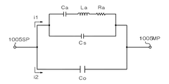
絶縁層1003の表面(上面)には、上記電極層1004S及び1004Mに導電接続された配線部1005SL,1005MLが伸びているとともに、これらの配線部1005SL,1005MLに導電接続された接続端子1005SP,1005MPが設けられている。これらの配線部1005SL,1005ML及び接続端子1005SP,1005MPは上記の配線層を構成する。配線層はアルミニウムなどの良導体で構成されることが好ましい。
On the surface (upper surface) of the insulating
本実施形態では、絶縁層1002上に電極層1004S,1004Mが形成され、絶縁層1002上にさらに積層されてなる絶縁層1003上に配線部1005SL,1005MLの一部及び接続端子1005SP,1005MPが形成されているが、配線部1005SL,1005MLの全てが絶縁層1003上に構成されていてもよく、さらに、図22(b)に点線で示すように絶縁層1003に延長部1003′を形成することで、電極層1004S,1004Mのうち電極1004Sa,1004Ma以外の部分を絶縁層1003上に形成してもよい。また、本実施形態では、一対の軸状の電極層1004S,1004Mが並列に配向配置されているが、従来構造のような櫛歯形状を備えた電極同士が相互に噛合する態様で対向配置されたものとしてもよい。
In this embodiment,
本実施形態のマイクロメカニカル静電振動子1000は、上記において説明した振動子構造体1004に相互に対向する電極1004Saと1004Maとを設けて、これらの電極のうちの少なくとも一方を振動させるようにし、図示例のように上記の電極のうちの主として振動する一方の電極1004Maが振動体であり、他方の電極1004Saは加振電極として構成される。ただし、上記の電極1004Maの代わりに上記第1乃至第6実施形態の振動体若しくは従動部を設け、上記の電極1004Saの代わりに上記第1乃至第6実施形態の加振電極を設けてもよい。このように構成することで、上記第1乃至第6実施形態の振動体又は加振電極に導電接続された配線層を有し、配線層と基板の距離が振動体又は加振電極と基板の距離よりも大きくなるように構成することができるため、振動子構造体と基板との間の寄生容量を低減することができる。
The micromechanical
図23は、本実施形態のマイクロメカニカル静電振動子1000をパッケージ内に封止した状態を示す概略縦断面図である。このマイクロメカニカル静電振動子1000は、上記電極層1004Mの電極1004Maを機械的に振動させることによって動作するものであるので、セラミックスや合成樹脂など絶縁素材で構成されるパッケージ1011,1012内に収容することが好ましい。特に、電極の振動を容易にするためには、パッケージ内を真空状態(真空パッケージ)とすることが好ましい。パッケージ1011には、内部端子1013S,1013Mと、この内部端子1013S,1013Mにそれぞれ導電接続された外部端子1014S,1014Mが形成されている。そして、上記接続端子1005SP,1005MPは、導電ワイヤ1015などによって内部端子1013S,1013Mにそれぞれ導電接続されている。
FIG. 23 is a schematic longitudinal sectional view showing a state in which the micromechanical
また、本実施形態のマイクロメカニカル静電振動子1000において、基板1001をシリコン基板などで構成することによって、基板1001内に所定の回路構造(例えば、半導体集積回路)を設けることができる。そして、この場合には、内部端子1016及びこれに導電接続された外部端子1017を設け、内部端子1016に導電ワイヤ1018などを介して上記回路構造を導電接続させることもできる。このようにすると、マイクロメカニカル静電振動子1000と所定の回路構造とを一体に構成することが可能になる。
なお、このマイクロメカニカル静電振動子1000は、図示例のようにパッケージ1011,1012に収容するのではなく、表面実装デバイス(SMD)などのように回路基板などに直接実装して用いることも可能である。
In the micromechanical
Note that the micromechanical
[製造方法]
次に、図25を参照して上記第7実施形態の製造方法について説明する。最初に、図25(a)に示すように、基板1001の表面上に絶縁層1002を形成する。絶縁層1002は、CVD法などで直接成膜してもよく、或いは、液状やペースト状の基材をスピンコーティング法、ロールコーティング法、印刷法などによって塗布し、加熱処理などによって硬化させてもよい。
[Production method]
Next, the manufacturing method of the seventh embodiment will be described with reference to FIG. First, as shown in FIG. 25A, an insulating
次に、図25(b)に示すように、絶縁層1002上にポリシリコンなどで構成される第1導体層1004C′と、SiO2、PSG(リンドープガラス)、有機樹脂などで構成される第1犠牲層1004D′とを形成する。これらはそれぞれフォトリソグラフィ法などを用いることによって容易に構成できる。その後、上記第1導体層1004C′の上にさらに同じ導体材料を配置し、上記第1犠牲層1004D′の上にさらに同じ犠牲材料を配置することによって、図25(c)に示すように、犠牲層1004Dによって支持された電極1004Sa,1004Ma(1004Saは図示せず)を有する電極層1004S,1004Mを形成する。ここで、上記各導体層はCVD法やスパッタリング法などで形成することができ、上記犠牲層はスパッタリング法やゾル−ゲル法などで形成することができる。
Next, as shown in FIG. 25 (b), the
次に、図26(a)に示すように、上記のように構成された電極構造をPSGや合成樹脂などで構成される保護層1006で被覆した状態とし、図26(b)に示すように、CVD法やスパッタリング法、ゾル−ゲル法などにより、電極形成領域に隣接する領域に絶縁層1003を形成する。この絶縁層1003は上記絶縁層1002と同様の方法で構成できるが、多孔質素材で絶縁層1003を構成する場合にはゾル−ゲル法を用いることができる。例えば、多孔質シリカは、アルコキシシランなどのガラス構成材料を含む溶液を塗布し、乾燥させる(アルコールなどの溶媒を揮発させる)ことによって構成できる。
Next, as shown in FIG. 26 (a), the electrode structure configured as described above is covered with a
本実施形態の場合、絶縁層1003は上記電極1004Sa,1004Maが動作する動作領域には形成されていない。このような選択的な絶縁層1003の形成方法としては、マスキング法、リフトオフ法、フォトリソグラフィ法などを用いることができる。このように、絶縁層1003を基板1001上において部分的に形成することは、絶縁層1003を全面的に基板1001上に形成した場合に生ずる可能性のある基板1001の反りなどを防止する上で有効である。また、絶縁層1003を動作領域の両側に形成したり、動作領域を取り囲むように形成したりすることにより、製造工程において動作領域上に構成された可動部分を有する脆弱な電極構造を保護することができるという利点もある。
In the case of this embodiment, the insulating
その後、上記の保護層1006を除去し、絶縁層1002,1003の表面上にアルミニウムなどの導体を蒸着法、スパッタリング法などを用いて成膜し、フォトリソグラフィ法等によってパターニングすることによって、図26(c)に示すように、上述の配線層、すなわち、配線部1005SL,1005ML及び接続端子1005SP,1005MPを形成する。そして、最後に、上記の犠牲層1004Dをエッチングなどによって除去することにより、図22に示す振動子構造体が形成される。
Thereafter, the
[作用効果]
図27は、上記実施形態のマイクロメカニカル静電振動子の等価回路図である。マイクロメカニカル静電振動子1000の等価回路には、接続端子1005SPと1005MPとの間に静電容量Ca,インダクタンスLa,抵抗Raの直列回路と、この直列回路と並列に接続される並列容量(short Capacitance)Csとが存在する。ここで、上記直列回路部分は静電振動子の入出力特性をもたらす部分であり、並列容量Csは電極1004Saと1004Maとの間の静電容量の定常成分に相当するものである。
[Function and effect]
FIG. 27 is an equivalent circuit diagram of the micromechanical electrostatic vibrator of the above embodiment. The equivalent circuit of the micromechanical
本実施形態のマイクロメカニカル静電振動子では、以上の回路構成に対してさらに並列に、電極層1004S、1004M、配線部1005SL、1005ML及び接続端子1005SP,1005MPと、基板1001との間の静電容量である寄生容量Coが存在する。そして、上記のように、配線部1005SL,1005ML及び接続端子1005SP,1005MPで構成される配線層が絶縁層1003の厚さti(図22(c)参照)分だけ電極1004Sa,1004Maよりも基板1001から離れた位置に配置されていることにより、上記の寄生容量Coは低減される。すなわち、配線層と基板1001との間に生ずる静電容量は、C=εS/t(Cは静電容量、εは誘電率、Sは電極面積、tは電極間距離)の式において電極間距離tが上記絶縁層1003の厚さti分だけ大きくなることによって小さくなる。また、この静電容量は、絶縁層1003の誘電率が絶縁層1002(上記請求項18の絶縁体に相当する。)の誘電率よりも小さくなれば、上記の式において誘電率εが実質的に小さくなることによってさらに小さくなる。
In the micromechanical electrostatic vibrator of the present embodiment, the electrostatic capacitance between the electrode layers 1004S and 1004M, the wiring portions 1005SL and 1005ML, the connection terminals 1005SP and 1005MP, and the
このように、上記配線層を電極よりも基板1001から離反させることにより寄生容量Coを小さくすることができるので、容量Co、Cs、Caに配分されていた電気エネルギーがより多くCsとCaに配分されるようになる。その結果、マイクロメカニカル静電振動子1000の出力電圧を大きくすることができ、また、駆動電圧を低減することも可能になる。
As described above, since the parasitic capacitance Co can be reduced by separating the wiring layer from the
図28は、本実施形態のマイクロメカニカル静電振動子1000のインピーダンスの周波数依存性を模式的に示すグラフである。ここで、図示二点鎖線は本実施形態のインピーダンスを示し、図示点線は従来構造の静電振動子のインピーダンスを示している。上記のように構成することによって寄生容量Coを小さくすることができるため、本実施形態では従来構造よりもインピーダンスが低減されている。
FIG. 28 is a graph schematically showing the frequency dependence of the impedance of the micromechanical
なお、上記実施形態では、絶縁層1002の上に絶縁層1003を部分的に積層しているが、絶縁層1002を動作領域に限定して形成し、絶縁層1003を動作領域に隣接する領域において基板1001上に直接形成してもよい。また、基板1001上に一体の絶縁層を形成しておき、この絶縁層のうち、動作領域上に形成されている部分を選択的にエッチングなどによって薄肉化することによって上記実施形態と同様の表面段差を形成するようにしてもよい。
Note that although the insulating
[第8実施形態]
図24は、本発明に係る第8実施形態のマイクロメカニカル静電振動子1100を示す概略縦断面図である。この実施形態では、基板1101、絶縁層1102、電極層1104S,1104M、電極1104Sa,1104Ma、配線部2005SL,2005ML、接続端子2005SP,2005MPはそれぞれ上記第1実施形態と同様であるので、それらの説明は省略する。
[Eighth Embodiment]
FIG. 24 is a schematic longitudinal sectional view showing a micromechanical
このマイクロメカニカル静電振動子1100においては、配線部1105SL,1105ML及び接続端子1105SP,1105MPで構成される配線層が絶縁層1103上に構成されている点では、上記第7実施形態と同様である。ただし、絶縁層1103の内部には空間1103aが設けられている。これによって、配線層と基板1101との間の誘電体の実質的な誘電率が空間1103aの厚さ分だけ絶縁層1103の誘電率よりもさらに低下するために、配線層と基板1101との間の静電容量もさらに低下する。したがって、上記の寄生容量Coをさらに低減できる。
The micromechanical
上記空間1103aは、例えば、絶縁層1103の第1層を形成した後に、図示しない犠牲層(ポリシリコン、PSG、有機樹脂などで構成できる。)を形成し、この犠牲層上にさらに絶縁層1103の第2層を積層し、その後、上記の犠牲層をエッチングなどで除去することによって構成できる。
In the space 1103 a, for example, after forming the first layer of the insulating
本実施形態において、上記空間は絶縁層1103の内部に形成されているが、本発明はこのような態様に限らず、空間が絶縁層1103と配線層の間に設けられていたり、絶縁層1103と絶縁層1102との間に設けられていたりしてもよいなど、配線層と基板1101との間であればいずれに空間が設けられていても構わない。
In this embodiment, the space is formed inside the insulating
[第9実施形態]
図29は、本発明に係る第9実施形態のマイクロメカニカル静電振動子の縦断面図である。このマイクロメカニカル静電振動子1200は、ガラス、石英、セラミックスなどの絶縁体で構成された基板1201上に、出力電極1203と、この出力電極1203に導電接続された支持部1204と、支持部1204に導電接続されて支持される振動体1205と、この振動体1205の両側において振動体1205の外縁に対向するように配置される一対の加振電極1207,1207とを備えた振動子構造体を有している。なお、この実施形態では、基板1201上に構成された振動子構造体が上記第1実施形態と同様に構成されているので、上記振動子構造体の詳細については説明を省略する。
[Ninth Embodiment]
FIG. 29 is a longitudinal sectional view of the micromechanical electrostatic vibrator of the ninth embodiment according to the present invention. The micromechanical
本実施形態では、基板1201が絶縁体からなるので、上記の振動子構造体と基板1201との間に寄生容量が生じないことから、寄生容量に起因する出力電圧の低下やエネルギー効率の低下を防止することができる。この点は、上記第7及び第8実施形態において説明したところと同様であるので、これ以上の詳細は省略する。ただし、本実施形態では、基板1201を絶縁体からなるものとすることにより、上記第7及び第8実施形態のように基板との間の寄生容量を低減するのではなく、当該寄生容量そのものがほとんど発生しないという点で、より効果的な構成となっている。特に、基板1201をガラスで構成することにより、基板材料を安価に入手できるとともに、製造時の各種処理を容易に実施することができるため、製造コストを低減することができる。
In this embodiment, since the
[第10実施形態]
図30は、本発明に係る第10実施形態のマイクロメカニカル静電振動子の縦断面図である。このマイクロメカニカル静電振動子1300は、ガラス、石英、セラミックスなどの絶縁体で構成された基板1301上に、基準電極1303と、この基準電極1303に導電接続された支持部1304と、支持部1304に導電接続されて支持される振動体1305と、この振動体1305の両側において振動体1305の外縁に対向するように配置される一対の加振電極1307,1307とを備えた振動子構造体を有している。なお、この実施形態では、基板1301上に構成された振動子構造体が上記第3実施形態と同様に構成されているので、上記振動子構造体の詳細については説明を省略する。
[Tenth embodiment]
FIG. 30 is a longitudinal sectional view of the micromechanical electrostatic vibrator according to the tenth embodiment of the present invention. The micromechanical
本実施形態では、基板1301が絶縁体からなるので、上記の振動子構造体と基板1301との間に寄生容量が生じないことから、寄生容量に起因する出力電圧の低下やエネルギー効率の低下を防止することができる。この点は、上記第9実施形態と同様である。また、基板1301をガラスで構成することにより、基板材料を安価に入手できるとともに、製造時の各種処理を容易に実施することができるため、製造コストを低減することができる。
In the present embodiment, since the
なお、上記の第2、第4乃至第8実施形態においても、上記の第9及び第10実施形態と同様に、その基板を絶縁体で構成することができる。これらの場合には、基板上に形成される絶縁層は不要となる。ただし、この絶縁層を他の目的、例えば、基板表面を平滑化する目的、基板上に構成される上記振動子構造体の密着性を高める目的などで絶縁体からなる基板上に形成することを何等妨げるものではない。 In the second, fourth to eighth embodiments, as in the ninth and tenth embodiments, the substrate can be made of an insulator. In these cases, an insulating layer formed on the substrate is not necessary. However, this insulating layer may be formed on a substrate made of an insulator for other purposes, for example, for the purpose of smoothing the surface of the substrate or for improving the adhesion of the vibrator structure formed on the substrate. It does not prevent anything.
[第11実施形態]
図31及び図32は、本発明に係る第11実施形態のマイクロメカニカル静電振動子の製造方法を示す工程図である。ここで、本実施形態は、上記第9実施形態のマイクロメカニカル静電振動子1200を製造する場合を例示するものであり、図31及び図32において、図29に示した部分と同一部分には同一の符号を付してある。また、以下の説明においてはSOI(Silicon On Insulator)基板1260を用いてマイクロメカニカル静電振動子1200を製造する場合を例に挙げて説明するが、シリコン基板1261上に絶縁膜及びポリシリコン(p−SiO)膜を形成することで、SOI基板1260を用いる場合とほぼ同様の工程で製造することもできる。
[Eleventh embodiment]
31 and 32 are process diagrams showing a method for manufacturing a micromechanical electrostatic vibrator of an eleventh embodiment according to the present invention. Here, this embodiment exemplifies the case of manufacturing the micromechanical
本実施形態では、図31(a)に示す通り、シリコン基板1261上に絶縁膜としての二酸化珪素(SiO2)からなる絶縁膜1262及び減圧気相成長(減圧CVD(Chemical Vapor Deposition))法を用いて形成され、その半導体層としてのシリコン層1263が順に形成されたSOI基板1260を用いる。上記シリコン基板1261は両面が研磨されており、厚さが約500μm程度である。また、絶縁膜1262は厚さが0.1μm程度に形成され、シリコン層1263は厚さが10〜20μm程度に形成される。
In this embodiment, as shown in FIG. 31A, an insulating
まず、図31(a)に示すSOI基板1260に形成されたシリコン層1263の上面全体に亘ってフォトレジスト(不図示)を塗布し、このフォトレジストに対して露光処理及び現像処理を行って、所定形状のレジストパターンを形成する。この処理で形成されるレジストパターンには、図29に示す振動子構造体の形成領域に開口部が形成される。より具体的には、振動体1205及び加振電極1207となるべき領域に開口部が形成される。ただし、出力電極1203及び支持部1204となるべき領域には開口部は形成されない。
First, a photoresist (not shown) is applied over the entire upper surface of the
次いで、このレジストパターンをマスクとしてSOI基板1260のシリコン層1263に対してエッチング処理を行い、シリコン層1263を数μm程度除去する。エッチング処理が完了すると、図31(b)に示す通り、シリコン層1263における振動体1205及び加振電極1207となるべき領域に凹部1263aが形成される。ただし、出力電極1203及び支持部1204となるべき箇所のシリコン層1263の領域1263bは除去されずに残される。その後、シリコン層1263上に形成されているレジストパターンは除去される。以上は上記の凹部形成工程を構成する。
Next, the
なお、上記の工程において、エッチングによって凹部1263aを形成するのではなく、図31(a)に点線で示すように、パターニングされたシリコン層を繰り返し積層することによって、図31(b)に示す凹部1263aを含む表面構造を形成してもよい。 In the above process, the concave portion 1263a is not formed by etching, but the patterned silicon layer is repeatedly laminated as shown by the dotted line in FIG. 31A, thereby forming the concave portion shown in FIG. A surface structure including 1263a may be formed.
次に、SOI基板1260に形成されたシリコン層1263とガラス等で構成される基板1201の表面とを向かい合わせて陽極接合により接合する。ここで陽極接合とは、ガラス等の絶縁基板とシリコン基板又は金属等とを密着接合する方法であって、重ね合わせた基板を加熱しするとともにシリコン基板を陽極として両者の間に高電圧を付加することにより、電気的二重層を発生させ、静電引力により基板同士を接合する方法である。基板1201としてガラス基板を用いる場合には、ガラス基板が軟化する程度に加熱が行われる。この陽極接合を用いることにより、図25(c)に示す通り、基板1201上にSOI基板1260が接合される。尚、SOI基板1260と基板1201とを陽極接合する際に、基板1201上に予め電極を形成し、この電極とシリコン層1263の上記出力電極1203や加振電極1207となるべき部位とが電気的に接続されるようにすることが好ましい。以上が上記の基板接合工程である。
Next, the
以上の工程が終了すると、基板1201に接合されたSOI基板1260の薄板化を行う。この処理では、SOI基板1260の絶縁膜1262をエッチングストップ層として用い、エッチングによりシリコン基板1261を除去する。このときのエッチングについては、ウェットエッチング及びドライエッチングの何れを用いることもできる。ドライエッチングを採用した場合、例えば誘導結合プラズマ(ICP)等を利用することができる。尚、このエッチングに先だって、絶縁膜1262が露出する直前までシリコン基板1261を研削(粗研磨)し、その後、上記のエッチングを行って残りのシリコン基板1261を除去することが好ましい。このようにすれば、処理時間を短縮して生産性を向上することができる。シリコン基板1261の研削にはCMP法(化学的機械的研磨法)を用いるのが好ましい。
When the above steps are completed, the
シリコン基板1201の除去を行うと、図32(a)に示す通り、基板1201上にシリコン層1263と絶縁膜1262とが形成された状態になる。次に、基板1201上に形成された絶縁膜1262上の全面に亘ってフォトレジスト(不図示)を塗布し、このフォトレジストに対して露光処理及び現像処理を行って所定形状のレジストパターンを形成する。次いで、このレジストパターンをマスクとして絶縁膜1262に対してエッチング処理を行って、図32(b)に示す通り、D−RIE(Deep Reactiv Ion Etching)用のマスクを形成する。マスクの形成が終了すると、絶縁膜1262上に形成されているレジストパターンを除去する。
When the
以上の工程が終了すると、絶縁膜1262をマスクとしてD−RIEによりシリコン層1263のエッチングを行い、図32(c)に示すように、基板1201上に出力電極1203、支持部1204、振動体1205及び加振電極1207を形成する。これが上記の振動子形成工程である。以上の工程を終えると、図31(b)に示す上記の凹部1263aに相当する部分が振動体1205及び加振電極1207と基板1201との間の空隙になり、図29に示すマイクロメカニカル静電振動子1200が形成される。
When the above steps are completed, the
[第12実施形態]
次に、本発明に係る第12実施形態のマイクロメカニカル静電振動子の製造方法について説明する。図33は、本実施形態のマイクロメカニカル静電振動子の製造方法の一部を示す工程図である。尚、図33において、図29に示した部分に対応する部分には同一の符号に′を付して示してある。この第12実施形態についても、上記の第11実施形態と同様に、上記の第9実施形態のマイクロメカニカル静電振動子1200に相当するものを製造する例を示したものである。したがって、上記第11実施形態と同様に他の実施形態のマイクロメカニカル静電振動子を製造する場合にも適用できる。また、上記の第11実施形態と同様に、以下の説明においてはSOI基板1260′を用いて製造する場合を例に挙げて説明するが、シリコン基板1261′上に絶縁膜及びポリシリコン(p−SiO)膜を形成することで、SOI基板1260′を用いる場合とほぼ同様の工程で製造することもできる。
[Twelfth embodiment]
Next, a manufacturing method of the micromechanical electrostatic vibrator according to the twelfth embodiment of the present invention will be described. FIG. 33 is a process diagram showing a part of the method for manufacturing the micromechanical electrostatic vibrator of the present embodiment. In FIG. 33, parts corresponding to those shown in FIG. 29 are denoted by the same reference numerals with '. In the twelfth embodiment as well, as in the eleventh embodiment, an example of manufacturing the one corresponding to the micromechanical
本実施形態では、まず図33(a)に示す通り、基板1201′の表面の全面に亘ってフォトレジスト(不図示)を塗布し、このフォトレジストに対して露光処理及び現像処理を行って、所定形状のレジストパターンを形成する。この処理で形成されるレジストパターンには、後の工程で張り合わされるSOI基板1260′の振動子構造体(振動体1205′及び加振電極1207′)が形成されるべき位置に向き合う部分に開口が形成されている。
In the present embodiment, first, as shown in FIG. 33A, a photoresist (not shown) is applied over the entire surface of the substrate 1201 ', and an exposure process and a development process are performed on the photoresist. A resist pattern having a predetermined shape is formed. In the resist pattern formed by this process, an opening is formed at a portion facing the position where the vibrator structure (vibrating
次いで、このレジストパターンをマスクとして基板1201′の表面に対してエッチング処理を行い、基板1201′の表面を数μm程度除去する。尚、支持部1204′となるべき箇所が接合される部位1201b′は除去せずに残しておく。エッチング処理が完了し、基板1201′上に形成されているレジストパターンを除去すると、上記部位1201b′に出力電極1203′を形成する。この出力電極1203′はアルミニウム等の金属やポリシリコンなどの半導体などで構成することができる。
Next, an etching process is performed on the surface of the
次に、SOI基板1260′に形成されたシリコン層1263′と基板1201′の表面とを向かい合わせて陽極接合により接合する。この陽極接合により、図33(b)に示す通り、基板1201′上にSOI基板1260′が接合される。尚、本実施形態においてもSOI基板1260′と基板1201とを陽極接合する際に、基板1201上に形成されている出力電極1203′やその他の配線などとシリコン層1263とが電気的に接続される。
Next, the
基板1201′とSOI基板1260′との接合を終えると、上記の実施形態と同様に、SOI基板1260′のシリコン基板1261′を除去する工程、D−RIEのマスクを絶縁膜1262′を用いて形成する工程、及び、絶縁膜1262をマスクとしてD−RIEを用いたエッチング工程を行うことにより、図33(c)に示すように、振動体1205′及び加振電極1207′が形成され、最終的に上記の図29に示すマイクロメカニカル静電振動子1200と等価な構造が構成される。
When the bonding between the
以上説明した通り、本実施形態においては、絶縁体の基板1201,1201′の表面とSOI基板1260,1260′のシリコン膜(活性層)1263,1263′とを向かい合わせて接合し、SOI基板1260,1260′に対して処理の加工を施し、振動子構造体を形成しているため、これらの振動子構造体と基板1201,1201′との間の寄生容量が生じないマイクロメカニカル静電振動子1200を安価に効率よく製造することができる。
As described above, in the present embodiment, the surfaces of the insulating
また、SOI基板1260,1260′と基板1201,1201′とを接合する前に、SOI基板1260,1260′に形成されたシリコン層1263,1263′、又は、基板1201,1201′の表面をエッチングにより除去して凹部1263a,1201a′を形成しているため、これらの凹部によって振動体1205,1205′と基板1201,1201′との間に空隙をきわめて容易に設けることができる。また、絶縁体の基板としてガラス基板を用いることにより、低い製造コストで高性能のマイクロメカニカル静電振動子を得ることができる。
Further, before bonding the
100…マイクロメカニカル静電振動子、101…基板、102…絶縁層、103…出力電極、104…支持部、105…振動体、105a,105b…円弧部、105c,105d…くびれ部、106…空隙、107…電極、110…入力回路、120…出力回路、300…マイクロメカニカル静電振動子、301…基板、302…絶縁層、303…基準電極、304…支持体、305…振動体、305a…支持部(中心部)、305b…外縁、305c…段差面、306…加振電極、307X,307Y…第2の加振電極、310A…入力回路、310B…出力回路、800…マイクロメカニカル静電振動子、801…基板、802…絶縁層、803…基準電極、805…振動体、805a…支持部、805b…従動部、805c…外縁、806…加振電極、810A…入力回路、810B…出力回路、1000…マイクロメカニカル静電振動子、1001…基板、1002…絶縁層、1003…絶縁層、1004S,1004M…電極層、1004Sa,1004Ma…電極、1005SL,1005ML…配線部、1005SP,1005MP…接続端子、1006…保護層、1103a…空間。
DESCRIPTION OF
Claims (10)
向配置される一対の加振電極と、該一対の加振電極に同相の交流電力を印加するための給
電手段と、前記振動体と前記加振電極との間の静電容量の変化に対応した出力を得るため
の検出手段とを有するマイクロメカニカル静電振動子において、
前記振動体の平面形状の輪郭は、円弧部と、該円弧部に両端が滑らかに連結されたくび
れ部とからなり、
前記振動体の平面形状は、少なくとも2つの円がお互いに重なった形状の輪郭を備え、
前記少なくとも2つの円がお互いに重なった形状であることによって形成される前記くび
れ部を備えた曲線状の輪郭を有する形状であることを特徴とするマイクロメカニカル静電
振動子。 A plate-like vibrating body, a pair of excitation electrodes disposed on both sides of the vibrating body with a gap to the outer periphery of the vibrating body, and in-phase AC power applied to the pair of excitation electrodes In a micromechanical electrostatic vibrator having power supply means for detecting and detecting means for obtaining an output corresponding to a change in capacitance between the vibrating body and the excitation electrode,
The outline of the planar shape of the vibrating body includes an arc portion and a constricted portion in which both ends are smoothly connected to the arc portion,
The planar shape of the vibrating body has an outline of a shape in which at least two circles overlap each other,
A micromechanical electrostatic vibrator having a curved outline having the constricted portion formed by the at least two circles overlapping each other.
形状に構成されていることを特徴とする請求項1に記載のマイクロメカニカル静電振動子
。 2. The micromechanical electrostatic vibrator according to claim 1, wherein the vibrating body is configured to be supported by a support portion formed on a substrate and spread around the support portion.
ン化合物層で構成されていることを特徴とする請求項1又は2に記載のマイクロメカニカ
ル静電振動子。 3. The micromechanical electrostatic vibrator according to claim 1, wherein the vibrating body includes a silicon layer or a silicon compound layer formed on a silicon substrate that is the substrate.
離が前記振動体又は前記加振電極と前記基板の距離よりも大きいことを特徴とする請求項
2又は3に記載のマイクロメカニカル静電振動子。 A wiring layer electrically connected to the vibrating body or the excitation electrode is provided, and a distance between the wiring layer and the substrate is larger than a distance between the vibrating body or the excitation electrode and the substrate. Item 4. The micromechanical electrostatic vibrator according to Item 2 or 3.
を備えた絶縁層上に形成されていることを特徴とする請求項4に記載のマイクロメカニカ
ル静電振動子。 The micro mechanical electrostatic according to claim 4, wherein the wiring layer is formed on an insulating layer having a surface farther from the substrate than a surface on which the vibrating body or the excitation electrode is formed. Vibrator.
記絶縁層は前記絶縁体よりも低い誘電率を有することを特徴とする請求項5に記載のマイ
クロメカニカル静電振動子。 The said vibrating body or the said excitation electrode is comprised on the surface of the insulator formed on the said board | substrate, and the said insulating layer has a dielectric constant lower than the said insulator. Micromechanical electrostatic vibrator.
カル静電振動子。 The micromechanical electrostatic vibrator according to claim 5, wherein the insulating layer is a porous film.
7のいずれか一項に記載のマイクロメカニカル静電振動子。 Micromechanical electrostatic vibrator as claimed in any one of claims 4 to 7, characterized in that the space is provided between the substrate and the wiring layer.
ロメカニカル静電振動子。 4. The micromechanical electrostatic vibrator according to claim 2, wherein the substrate is a substrate made of an insulator.
電振動子。 The micromechanical electrostatic vibrator according to claim 9, wherein the substrate is made of glass.
Priority Applications (7)
| Application Number | Priority Date | Filing Date | Title |
|---|---|---|---|
| JP2004244835A JP4086023B2 (en) | 2003-12-04 | 2004-08-25 | Micromechanical electrostatic vibrator |
| US10/990,411 US7215061B2 (en) | 2003-12-04 | 2004-11-18 | Micromechanical electrostatic resonator |
| ES04027961T ES2277188T3 (en) | 2003-12-04 | 2004-11-25 | MICROMECHANICAL ELECTROSTATIC RESONATOR. |
| AT04027961T ATE352900T1 (en) | 2003-12-04 | 2004-11-25 | MICROMECHANICAL ELECTROSTATIC RESONATOR |
| DE602004004484T DE602004004484T2 (en) | 2003-12-04 | 2004-11-25 | Micromechanical electrostatic resonator |
| EP04027961A EP1538747B1 (en) | 2003-12-04 | 2004-11-25 | Micromechanical electrostatic resonator |
| CNB2004100955860A CN100438334C (en) | 2003-12-04 | 2004-12-02 | Micromechanical electrostatic resonator |
Applications Claiming Priority (5)
| Application Number | Priority Date | Filing Date | Title |
|---|---|---|---|
| JP2003405839 | 2003-12-04 | ||
| JP2004038468 | 2004-02-16 | ||
| JP2004054182 | 2004-02-27 | ||
| JP2004054180 | 2004-02-27 | ||
| JP2004244835A JP4086023B2 (en) | 2003-12-04 | 2004-08-25 | Micromechanical electrostatic vibrator |
Publications (3)
| Publication Number | Publication Date |
|---|---|
| JP2005271191A JP2005271191A (en) | 2005-10-06 |
| JP2005271191A5 JP2005271191A5 (en) | 2007-06-14 |
| JP4086023B2 true JP4086023B2 (en) | 2008-05-14 |
Family
ID=34468539
Family Applications (1)
| Application Number | Title | Priority Date | Filing Date |
|---|---|---|---|
| JP2004244835A Expired - Fee Related JP4086023B2 (en) | 2003-12-04 | 2004-08-25 | Micromechanical electrostatic vibrator |
Country Status (7)
| Country | Link |
|---|---|
| US (1) | US7215061B2 (en) |
| EP (1) | EP1538747B1 (en) |
| JP (1) | JP4086023B2 (en) |
| CN (1) | CN100438334C (en) |
| AT (1) | ATE352900T1 (en) |
| DE (1) | DE602004004484T2 (en) |
| ES (1) | ES2277188T3 (en) |
Cited By (1)
| Publication number | Priority date | Publication date | Assignee | Title |
|---|---|---|---|---|
| US7649426B2 (en) | 2006-09-12 | 2010-01-19 | Cts Corporation | Apparatus and method for temperature compensation of crystal oscillators |
Families Citing this family (89)
| Publication number | Priority date | Publication date | Assignee | Title |
|---|---|---|---|---|
| US7654140B2 (en) * | 2002-03-12 | 2010-02-02 | Cornell Research Foundation, Inc. | Heat pumped parametric MEMS device |
| FR2872501B1 (en) * | 2004-07-01 | 2006-11-03 | Commissariat Energie Atomique | COMPOSITE MICRO-DETERIORATOR WITH HIGH DEFORMATION |
| CN101103515B (en) * | 2005-01-07 | 2010-10-13 | 波士顿大学托管委员会 | Nanomechanical oscillator |
| US20110068834A1 (en) * | 2005-01-07 | 2011-03-24 | Trustees Of Boston University | Electro-mechanical oscillating devices and associated methods |
| JP4484778B2 (en) * | 2005-07-08 | 2010-06-16 | 富士フイルム株式会社 | Small thin film movable element, small thin film movable element array, and driving method of small thin film movable element |
| US7843283B2 (en) * | 2005-11-09 | 2010-11-30 | Cornell Research Foundation, Inc. | MEMS controlled oscillator |
| US7808253B2 (en) * | 2005-12-02 | 2010-10-05 | Semiconductor Energy Laboratory Co., Ltd. | Test method of microstructure body and micromachine |
| US9130602B2 (en) * | 2006-01-18 | 2015-09-08 | Qualcomm Incorporated | Method and apparatus for delivering energy to an electrical or electronic device via a wireless link |
| US8447234B2 (en) * | 2006-01-18 | 2013-05-21 | Qualcomm Incorporated | Method and system for powering an electronic device via a wireless link |
| JP5309316B2 (en) * | 2006-02-06 | 2013-10-09 | 国立大学法人東北大学 | Chip element |
| JP2008092788A (en) * | 2006-09-04 | 2008-04-17 | Seiko Epson Corp | Electric motor, method of manufacturing the electric motor, electric motor for electromagnetic coil, electronic equipment and equipment using fuel cells |
| US8314665B2 (en) * | 2006-09-20 | 2012-11-20 | Trustees Of Boston University | Nano electromechanical integrated-circuit filter |
| US8487715B2 (en) * | 2006-09-20 | 2013-07-16 | Trustees Of Boston University | Nano electromechanical integrated-circuit bank and switch |
| US7545239B2 (en) * | 2006-12-20 | 2009-06-09 | Sitime Inc. | Serrated MEMS resonators |
| US7545238B2 (en) * | 2006-12-20 | 2009-06-09 | Sitime Inc. | Serrated MEMS resonators |
| US7545237B2 (en) * | 2006-12-20 | 2009-06-09 | Sitime Inc. | Serrated MEMS resonators |
| US9774086B2 (en) | 2007-03-02 | 2017-09-26 | Qualcomm Incorporated | Wireless power apparatus and methods |
| US8482157B2 (en) * | 2007-03-02 | 2013-07-09 | Qualcomm Incorporated | Increasing the Q factor of a resonator |
| JP5028646B2 (en) * | 2007-06-07 | 2012-09-19 | 独立行政法人 宇宙航空研究開発機構 | Small oscillator |
| US9124120B2 (en) * | 2007-06-11 | 2015-09-01 | Qualcomm Incorporated | Wireless power system and proximity effects |
| JP2009014768A (en) | 2007-06-29 | 2009-01-22 | Fujitsu Ltd | Micro electro mechanical systems device and method of manufacturing the same |
| JP5028185B2 (en) * | 2007-08-28 | 2012-09-19 | 三洋電機株式会社 | Electrostatic generator |
| JP5055596B2 (en) * | 2007-08-29 | 2012-10-24 | セイコーインスツル株式会社 | Oscillator and oscillator having the oscillator |
| EP2188863A1 (en) * | 2007-09-13 | 2010-05-26 | QUALCOMM Incorporated | Maximizing power yield from wireless power magnetic resonators |
| CN101828300A (en) * | 2007-09-17 | 2010-09-08 | 高通股份有限公司 | Transmitters and receivers for wireless energy transfer |
| JP2009088854A (en) * | 2007-09-28 | 2009-04-23 | Sanyo Electric Co Ltd | Micro mechanical resonator and its manufacturing method |
| US8772999B2 (en) | 2007-10-11 | 2014-07-08 | Sand 9, Inc. | Signal amplification by hierarchal resonating structures |
| US8373514B2 (en) | 2007-10-11 | 2013-02-12 | Qualcomm Incorporated | Wireless power transfer using magneto mechanical systems |
| US8629576B2 (en) * | 2008-03-28 | 2014-01-14 | Qualcomm Incorporated | Tuning and gain control in electro-magnetic power systems |
| US7990229B2 (en) | 2008-04-01 | 2011-08-02 | Sand9, Inc. | Methods and devices for compensating a signal using resonators |
| US8044736B2 (en) * | 2008-04-29 | 2011-10-25 | Sand9, Inc. | Timing oscillators and related methods |
| US8044737B2 (en) * | 2008-04-29 | 2011-10-25 | Sand9, Inc. | Timing oscillators and related methods |
| US8410868B2 (en) | 2009-06-04 | 2013-04-02 | Sand 9, Inc. | Methods and apparatus for temperature control of devices and mechanical resonating structures |
| US8766512B2 (en) * | 2009-03-31 | 2014-07-01 | Sand 9, Inc. | Integration of piezoelectric materials with substrates |
| US8476809B2 (en) | 2008-04-29 | 2013-07-02 | Sand 9, Inc. | Microelectromechanical systems (MEMS) resonators and related apparatus and methods |
| US20090273242A1 (en) * | 2008-05-05 | 2009-11-05 | Nigelpower, Llc | Wireless Delivery of power to a Fixed-Geometry power part |
| CN102037644B (en) * | 2008-05-19 | 2014-12-31 | Nxp股份有限公司 | Improved mems resonator |
| US20090299918A1 (en) * | 2008-05-28 | 2009-12-03 | Nigelpower, Llc | Wireless delivery of power to a mobile powered device |
| JP5505596B2 (en) | 2008-06-18 | 2014-05-28 | セイコーエプソン株式会社 | Resonant circuit, oscillation circuit, filter circuit, and electronic device |
| US8111108B2 (en) * | 2008-07-29 | 2012-02-07 | Sand9, Inc. | Micromechanical resonating devices and related methods |
| DE102008042350A1 (en) * | 2008-09-25 | 2010-04-01 | Robert Bosch Gmbh | Micromechanical component and method for its production |
| US20100155883A1 (en) * | 2008-10-31 | 2010-06-24 | Trustees Of Boston University | Integrated mems and ic systems and related methods |
| US8686614B2 (en) * | 2008-12-17 | 2014-04-01 | Sand 9, Inc. | Multi-port mechanical resonating devices and related methods |
| US8689426B2 (en) | 2008-12-17 | 2014-04-08 | Sand 9, Inc. | Method of manufacturing a resonating structure |
| WO2010077313A1 (en) | 2008-12-17 | 2010-07-08 | Sand9, Inc. | Mechanical resonating structures including a temperature compensation structure |
| US8456250B2 (en) * | 2009-02-04 | 2013-06-04 | Sand 9, Inc. | Methods and apparatus for tuning devices having resonators |
| US8395456B2 (en) * | 2009-02-04 | 2013-03-12 | Sand 9, Inc. | Variable phase amplifier circuit and method of use |
| WO2010090731A2 (en) * | 2009-02-04 | 2010-08-12 | Sand9, Inc. | Methods and apparatus for tuning devices having mechanical resonators |
| WO2010110918A1 (en) * | 2009-03-26 | 2010-09-30 | Sand9, Inc. | Mechanical resonating structures and methods |
| US9048811B2 (en) | 2009-03-31 | 2015-06-02 | Sand 9, Inc. | Integration of piezoelectric materials with substrates |
| US8174170B1 (en) | 2009-05-13 | 2012-05-08 | Sand 9, Inc. | Methods and apparatus for mechanical resonating structures |
| US8115573B2 (en) * | 2009-05-29 | 2012-02-14 | Infineon Technologies Ag | Resonance frequency tunable MEMS device |
| US8513863B2 (en) | 2009-06-11 | 2013-08-20 | Qualcomm Mems Technologies, Inc. | Piezoelectric resonator with two layers |
| US8063720B2 (en) * | 2009-08-31 | 2011-11-22 | Georgia Tech Research Corporation | MEMS resonators having resonator bodies therein with concave-shaped sides that support high quality factor and low temperature coefficient of resonant frequency |
| US8664836B1 (en) | 2009-09-18 | 2014-03-04 | Sand 9, Inc. | Passivated micromechanical resonators and related methods |
| FR2954021B1 (en) * | 2009-12-10 | 2012-08-03 | Commissariat Energie Atomique | COMPENSATED MICRO / RESONATOR WITH IMPROVED CAPACITIVE DETECTION AND METHOD FOR PRODUCING THE SAME |
| US8704604B2 (en) | 2009-12-23 | 2014-04-22 | Sand 9, Inc. | Oscillators having arbitrary frequencies and related systems and methods |
| US8604888B2 (en) * | 2009-12-23 | 2013-12-10 | Sand 9, Inc. | Oscillators having arbitrary frequencies and related systems and methods |
| US8228127B2 (en) * | 2009-12-23 | 2012-07-24 | Sand 9, Inc. | Oscillators having arbitrary frequencies and related systems and methods |
| WO2011109382A1 (en) | 2010-03-01 | 2011-09-09 | Sand9, Inc. | Microelectromechanical gyroscopes and related apparatus and methods |
| JP5627258B2 (en) * | 2010-03-23 | 2014-11-19 | キヤノン株式会社 | Vibration type actuator and manufacturing method thereof |
| JP5930595B2 (en) * | 2010-04-06 | 2016-06-08 | キヤノン株式会社 | Vibrating actuator, vibrator and vibrator manufacturing method |
| WO2011133682A1 (en) | 2010-04-20 | 2011-10-27 | Guiti Zolfagharkhani | Microelectromechanical gyroscopes and related apparatus and methods |
| JP5355515B2 (en) | 2010-05-06 | 2013-11-27 | 株式会社村田製作所 | Touch panel, touch input device, and control method thereof |
| KR101158200B1 (en) * | 2010-06-04 | 2012-06-19 | 삼성전기주식회사 | Optical Image Stabilizer and Method of manufacturing the same |
| EP2400662B1 (en) | 2010-06-18 | 2015-11-04 | Nxp B.V. | Micro-electromechanical resonator geometry |
| WO2012040043A1 (en) | 2010-09-20 | 2012-03-29 | Sand9, Inc. | Resonant sensing using extensional modes of a plate |
| JP2012119822A (en) | 2010-11-30 | 2012-06-21 | Seiko Epson Corp | Electronic device, electronic apparatus, and manufacturing method of the electronic device |
| JP5630243B2 (en) | 2010-11-30 | 2014-11-26 | セイコーエプソン株式会社 | Electronic device, electronic apparatus, and method of manufacturing electronic device |
| JP2012178710A (en) * | 2011-02-25 | 2012-09-13 | Sanyo Electric Co Ltd | Mems device and manufacturing method thereof |
| US8501515B1 (en) | 2011-02-25 | 2013-08-06 | Integrated Device Technology Inc. | Methods of forming micro-electromechanical resonators using passive compensation techniques |
| JP5875243B2 (en) * | 2011-04-06 | 2016-03-02 | キヤノン株式会社 | Electromechanical transducer and method for manufacturing the same |
| US8610336B1 (en) | 2011-09-30 | 2013-12-17 | Integrated Device Technology Inc | Microelectromechanical resonators having resistive heating elements therein configured to provide frequency tuning through convective heating of resonator bodies |
| US9383208B2 (en) | 2011-10-13 | 2016-07-05 | Analog Devices, Inc. | Electromechanical magnetometer and applications thereof |
| JP5516904B2 (en) * | 2011-11-11 | 2014-06-11 | セイコーエプソン株式会社 | Manufacturing method of semiconductor device |
| JP5516903B2 (en) * | 2011-11-11 | 2014-06-11 | セイコーエプソン株式会社 | Manufacturing method of semiconductor device |
| US9299910B1 (en) | 2012-05-17 | 2016-03-29 | Analog Devices, Inc. | Resonator anchors and related apparatus and methods |
| US9954513B1 (en) | 2012-12-21 | 2018-04-24 | Analog Devices, Inc. | Methods and apparatus for anchoring resonators |
| US9634227B1 (en) | 2013-03-06 | 2017-04-25 | Analog Devices, Inc. | Suppression of spurious modes of vibration for resonators and related apparatus and methods |
| US9601267B2 (en) | 2013-07-03 | 2017-03-21 | Qualcomm Incorporated | Wireless power transmitter with a plurality of magnetic oscillators |
| JP2015080012A (en) * | 2013-10-15 | 2015-04-23 | セイコーエプソン株式会社 | Vibrator, oscillator, electronic apparatus and movable body |
| JP2015080013A (en) * | 2013-10-15 | 2015-04-23 | セイコーエプソン株式会社 | Vibrator, oscillator, electronic apparatus and movable body |
| JP2016040984A (en) * | 2014-08-13 | 2016-03-24 | セイコーエプソン株式会社 | Piezoelectric drive device and drive method of the same, robot and drive method of the robot |
| CN105375812A (en) | 2014-08-13 | 2016-03-02 | 精工爱普生株式会社 | Piezoelectric driving device and driving method therefor, and robot and driving method therefor |
| DE102016112101B4 (en) * | 2016-07-01 | 2018-08-02 | Physik Instrumente (Pi) Gmbh & Co. Kg | Device comprising an ultrasonic actuator and a mounting device, wherein the ultrasonic actuator is arranged on the mounting device |
| US10800649B2 (en) | 2016-11-28 | 2020-10-13 | Analog Devices International Unlimited Company | Planar processing of suspended microelectromechanical systems (MEMS) devices |
| CN107147370B (en) * | 2017-04-10 | 2020-05-22 | 西安交通大学 | MEMS oscillator based on vibration mode coupling and control method |
| US10843920B2 (en) | 2019-03-08 | 2020-11-24 | Analog Devices International Unlimited Company | Suspended microelectromechanical system (MEMS) devices |
| CN111131949A (en) * | 2019-12-25 | 2020-05-08 | 中国航空工业集团公司西安飞机设计研究所 | Flexible vibration device |
Family Cites Families (8)
| Publication number | Priority date | Publication date | Assignee | Title |
|---|---|---|---|---|
| US6369374B1 (en) | 1999-10-15 | 2002-04-09 | Agere Systems Guardian Corp. | Filter including a micro-mechanical resonator |
| US6628177B2 (en) * | 2000-08-24 | 2003-09-30 | The Regents Of The University Of Michigan | Micromechanical resonator device and micromechanical device utilizing same |
| US20020070816A1 (en) * | 2000-08-24 | 2002-06-13 | Wan-Thai Hsu | Method for making micromechanical structures having at least one lateral, small gap therebetween and micromechanical device produced thereby |
| AU2003290513A1 (en) * | 2002-08-07 | 2004-04-08 | Georgia Tech Research Corporation | Capacitive resonators and methods of fabrication |
| US6985051B2 (en) * | 2002-12-17 | 2006-01-10 | The Regents Of The University Of Michigan | Micromechanical resonator device and method of making a micromechanical device |
| US6894586B2 (en) * | 2003-05-21 | 2005-05-17 | The Regents Of The University Of California | Radial bulk annular resonator using MEMS technology |
| US7056757B2 (en) * | 2003-11-25 | 2006-06-06 | Georgia Tech Research Corporation | Methods of forming oxide masks with submicron openings and microstructures formed thereby |
| WO2005074502A2 (en) * | 2004-01-21 | 2005-08-18 | The Regents Of The University Of Michigan | High-q micromechanical resonator devices and filters utilizing same |
-
2004
- 2004-08-25 JP JP2004244835A patent/JP4086023B2/en not_active Expired - Fee Related
- 2004-11-18 US US10/990,411 patent/US7215061B2/en not_active Expired - Fee Related
- 2004-11-25 ES ES04027961T patent/ES2277188T3/en active Active
- 2004-11-25 DE DE602004004484T patent/DE602004004484T2/en active Active
- 2004-11-25 AT AT04027961T patent/ATE352900T1/en active
- 2004-11-25 EP EP04027961A patent/EP1538747B1/en not_active Not-in-force
- 2004-12-02 CN CNB2004100955860A patent/CN100438334C/en not_active Expired - Fee Related
Cited By (1)
| Publication number | Priority date | Publication date | Assignee | Title |
|---|---|---|---|---|
| US7649426B2 (en) | 2006-09-12 | 2010-01-19 | Cts Corporation | Apparatus and method for temperature compensation of crystal oscillators |
Also Published As
| Publication number | Publication date |
|---|---|
| CN100438334C (en) | 2008-11-26 |
| CN1625046A (en) | 2005-06-08 |
| ES2277188T3 (en) | 2007-07-01 |
| EP1538747A1 (en) | 2005-06-08 |
| EP1538747B1 (en) | 2007-01-24 |
| DE602004004484T2 (en) | 2007-11-08 |
| ATE352900T1 (en) | 2007-02-15 |
| DE602004004484D1 (en) | 2007-03-15 |
| US20050151442A1 (en) | 2005-07-14 |
| JP2005271191A (en) | 2005-10-06 |
| US7215061B2 (en) | 2007-05-08 |
Similar Documents
| Publication | Publication Date | Title |
|---|---|---|
| JP4086023B2 (en) | Micromechanical electrostatic vibrator | |
| US8742873B2 (en) | MEMS resonator devices | |
| US9923545B2 (en) | Compound spring MEMS resonators for frequency and timing generation | |
| JP4645227B2 (en) | Vibrator structure and manufacturing method thereof | |
| JP4690436B2 (en) | MEMS resonator, MEMS oscillation circuit, and MEMS device | |
| JP4838149B2 (en) | Torsional resonator and filter using the same | |
| US7522019B2 (en) | Internal electrostatic transduction structures for bulk-mode micromechanical resonators | |
| WO2004013893A2 (en) | Piezo electric on seminconductor on- insulator resonator | |
| US9866200B2 (en) | Multiple coil spring MEMS resonator | |
| JP2022529131A (en) | Micro electromechanical resonator | |
| JP4458081B2 (en) | Flap vibrator and integrated circuit including flap vibrator | |
| US20070035200A1 (en) | Microelectromechanical system comprising a beam that undergoes flexural deformation | |
| JP2007175577A (en) | Mems vibrator | |
| JP2012129605A (en) | Mems vibrator, oscillator, and manufacturing method of mems vibrator | |
| US9160305B1 (en) | Capacitively and piezoelectrically transduced micromechanical resonators | |
| JP5671742B2 (en) | Method for arranging electrode structure element and vibration structure element close to each other and MEMS device using the same | |
| JP2006319387A (en) | Mems resonator | |
| JP2009088685A (en) | Electromechanical element, and semiconductor device | |
| TW201401773A (en) | MEMS resonator and the method of processing the signal and manufacturing | |
| JP2009212887A (en) | Electrostatic vibrator and use thereof | |
| JP2009212888A (en) | Electrostatic vibrator and use thereof | |
| JP2006303558A (en) | Mems resonator | |
| JP5135628B2 (en) | Oscillator and oscillator using the same | |
| JP4739261B2 (en) | MEMS vibrator | |
| US8760234B2 (en) | MEMS vibrator and oscillator |
Legal Events
| Date | Code | Title | Description |
|---|---|---|---|
| A521 | Request for written amendment filed |
Free format text: JAPANESE INTERMEDIATE CODE: A523 Effective date: 20070420 |
|
| A871 | Explanation of circumstances concerning accelerated examination |
Free format text: JAPANESE INTERMEDIATE CODE: A871 Effective date: 20070420 |
|
| A975 | Report on accelerated examination |
Free format text: JAPANESE INTERMEDIATE CODE: A971005 Effective date: 20070514 |
|
| A131 | Notification of reasons for refusal |
Free format text: JAPANESE INTERMEDIATE CODE: A131 Effective date: 20070522 |
|
| A521 | Request for written amendment filed |
Free format text: JAPANESE INTERMEDIATE CODE: A523 Effective date: 20070719 |
|
| A131 | Notification of reasons for refusal |
Free format text: JAPANESE INTERMEDIATE CODE: A131 Effective date: 20070821 |
|
| A521 | Request for written amendment filed |
Free format text: JAPANESE INTERMEDIATE CODE: A523 Effective date: 20071015 |
|
| A131 | Notification of reasons for refusal |
Free format text: JAPANESE INTERMEDIATE CODE: A131 Effective date: 20071106 |
|
| A521 | Request for written amendment filed |
Free format text: JAPANESE INTERMEDIATE CODE: A523 Effective date: 20071227 |
|
| TRDD | Decision of grant or rejection written | ||
| A01 | Written decision to grant a patent or to grant a registration (utility model) |
Free format text: JAPANESE INTERMEDIATE CODE: A01 Effective date: 20080129 |
|
| A61 | First payment of annual fees (during grant procedure) |
Free format text: JAPANESE INTERMEDIATE CODE: A61 Effective date: 20080211 |
|
| FPAY | Renewal fee payment (event date is renewal date of database) |
Free format text: PAYMENT UNTIL: 20110228 Year of fee payment: 3 |
|
| R150 | Certificate of patent or registration of utility model |
Ref document number: 4086023 Country of ref document: JP Free format text: JAPANESE INTERMEDIATE CODE: R150 Free format text: JAPANESE INTERMEDIATE CODE: R150 |
|
| FPAY | Renewal fee payment (event date is renewal date of database) |
Free format text: PAYMENT UNTIL: 20110228 Year of fee payment: 3 |
|
| FPAY | Renewal fee payment (event date is renewal date of database) |
Free format text: PAYMENT UNTIL: 20120229 Year of fee payment: 4 |
|
| FPAY | Renewal fee payment (event date is renewal date of database) |
Free format text: PAYMENT UNTIL: 20130228 Year of fee payment: 5 |
|
| FPAY | Renewal fee payment (event date is renewal date of database) |
Free format text: PAYMENT UNTIL: 20130228 Year of fee payment: 5 |
|
| S531 | Written request for registration of change of domicile |
Free format text: JAPANESE INTERMEDIATE CODE: R313531 |
|
| R350 | Written notification of registration of transfer |
Free format text: JAPANESE INTERMEDIATE CODE: R350 |
|
| LAPS | Cancellation because of no payment of annual fees |