JP4073265B2 - Inspection apparatus and inspection method - Google Patents
Inspection apparatus and inspection methodInfo
- Publication number
- JP4073265B2 JP4073265B2 JP2002199595A JP2002199595A JP4073265B2 JP 4073265 B2 JP4073265 B2 JP 4073265B2 JP 2002199595 A JP2002199595 A JP 2002199595A JP 2002199595 A JP2002199595 A JP 2002199595A JP 4073265 B2 JP4073265 B2 JP 4073265B2
- Authority
- JP
- Japan
- Prior art keywords
- inspection
- defect
- data
- sensitivity
- pattern
- Prior art date
- Legal status (The legal status is an assumption and is not a legal conclusion. Google has not performed a legal analysis and makes no representation as to the accuracy of the status listed.)
- Expired - Fee Related
Links
Images


Classifications
-
- G—PHYSICS
- G06—COMPUTING; CALCULATING OR COUNTING
- G06T—IMAGE DATA PROCESSING OR GENERATION, IN GENERAL
- G06T7/00—Image analysis
- G06T7/0002—Inspection of images, e.g. flaw detection
- G06T7/0004—Industrial image inspection
- G06T7/0006—Industrial image inspection using a design-rule based approach
-
- G—PHYSICS
- G01—MEASURING; TESTING
- G01N—INVESTIGATING OR ANALYSING MATERIALS BY DETERMINING THEIR CHEMICAL OR PHYSICAL PROPERTIES
- G01N21/00—Investigating or analysing materials by the use of optical means, i.e. using sub-millimetre waves, infrared, visible or ultraviolet light
- G01N21/84—Systems specially adapted for particular applications
- G01N21/88—Investigating the presence of flaws or contamination
- G01N21/95—Investigating the presence of flaws or contamination characterised by the material or shape of the object to be examined
- G01N21/956—Inspecting patterns on the surface of objects
- G01N21/95607—Inspecting patterns on the surface of objects using a comparative method
-
- G—PHYSICS
- G03—PHOTOGRAPHY; CINEMATOGRAPHY; ANALOGOUS TECHNIQUES USING WAVES OTHER THAN OPTICAL WAVES; ELECTROGRAPHY; HOLOGRAPHY
- G03F—PHOTOMECHANICAL PRODUCTION OF TEXTURED OR PATTERNED SURFACES, e.g. FOR PRINTING, FOR PROCESSING OF SEMICONDUCTOR DEVICES; MATERIALS THEREFOR; ORIGINALS THEREFOR; APPARATUS SPECIALLY ADAPTED THEREFOR
- G03F1/00—Originals for photomechanical production of textured or patterned surfaces, e.g., masks, photo-masks, reticles; Mask blanks or pellicles therefor; Containers specially adapted therefor; Preparation thereof
- G03F1/68—Preparation processes not covered by groups G03F1/20 - G03F1/50
- G03F1/82—Auxiliary processes, e.g. cleaning or inspecting
- G03F1/84—Inspecting
-
- G—PHYSICS
- G06—COMPUTING; CALCULATING OR COUNTING
- G06T—IMAGE DATA PROCESSING OR GENERATION, IN GENERAL
- G06T2207/00—Indexing scheme for image analysis or image enhancement
- G06T2207/30—Subject of image; Context of image processing
- G06T2207/30108—Industrial image inspection
- G06T2207/30148—Semiconductor; IC; Wafer
Landscapes
- Physics & Mathematics (AREA)
- Engineering & Computer Science (AREA)
- General Physics & Mathematics (AREA)
- Chemical & Material Sciences (AREA)
- Biochemistry (AREA)
- Theoretical Computer Science (AREA)
- Health & Medical Sciences (AREA)
- Life Sciences & Earth Sciences (AREA)
- Quality & Reliability (AREA)
- Analytical Chemistry (AREA)
- Computer Vision & Pattern Recognition (AREA)
- General Health & Medical Sciences (AREA)
- Immunology (AREA)
- Pathology (AREA)
- Testing Or Measuring Of Semiconductors Or The Like (AREA)
- Investigating Materials By The Use Of Optical Means Adapted For Particular Applications (AREA)
- Preparing Plates And Mask In Photomechanical Process (AREA)
Description
【0001】
【発明の属する技術分野】
本発明は、検査装置及び検査方法に関し、特にフォトマスクまたはウェハーを検査する検査装置及び検査方法に関する。
【0002】
【従来の技術】
LSI(Large-Scale Integrated circuit)の微細化が進むなかで、近年、ウェハーのみならず、LSI作成時に用いられる、レチクルなどのフォトマスクの精度も高まっている。
【0003】
一方、フォトマスクやウェハーの欠陥を検出する検査装置においても、検査感度の向上が求められている。
図12は、従来の検査装置の構成を示すブロック図である。
【0004】
検査装置100は、実パターンを描画する時に使用した設計データと比較する「die to database検査」を行う検査装置100である。ここで、検査装置100は、設計データをもとに検査用の検査データを生成する検査データ生成部101と、検査条件を設定する検査条件設定部102と、被検査対象110であるフォトマスクやウェハーの実パターンを画像データとして取り込む画像取得部103と、比較のために、検査データ及び被検査データを画像変換する画像変換部104、105と、被検査データと検査データとを比較して欠陥を検出する比較判断部106と、比較されて検出された欠陥を記憶する欠陥記憶部107と、被検査対象110を載せるためのステージ108aの駆動及び、検査装置100全体を制御する検査/駆動制御部108と、から構成される。
【0005】
この検査装置100において、検査データ生成部101に設計データが入力されると、検査に適したフォーマットの検査データが生成される。さらに、検査条件設定部102において検査感度などを設定すると、検査が開始される。ここで、検査データは、画像変換部104にて画像に変換され比較判断部106に入力される。これと同期して、画像取得部103で得られた被検査対象110の実パターンが被検査データとして画像変換部105に送られ、ここで画像変換されて比較判断部106に入力される。比較判断部106では、検査条件設定部102で設定された検査感度を参照し、2つの画像データを比較して、欠陥があるか否かを判断する。ここで、欠陥が検出された場合、欠陥は欠陥記憶部107に記憶される。検査/駆動制御部108では、ステージ108aをスキャンすることにより、被検査対象110の全てのエリアについて検査を行う。
【0006】
このように、従来の検査装置100は、被検査データと検査データを比較し、それが異なれば、欠陥として検出するようにしていた。
【0007】
【発明が解決しようとする課題】
しかし、従来の検査装置100では、検査感度を上げた場合、無欠陥箇所であるにもかかわらず、欠陥と誤認されてしまう擬似欠陥が発生するという問題があった。また、フォトマスクやウェハーの欠陥場所によっては、性能や特性に影響されない欠陥もあり、問題のない欠陥に対しても修正するなどの工数をかけており、手間であるという問題があった。
【0008】
本発明はこのような点に鑑みてなされたものであり、検査から修正までの時間短縮が可能な検査装置を提供することを目的とする。
また、本発明の他の目的は、検査から修正までの時間短縮が可能な検査方法を提供することである。
【0009】
【課題を解決するための手段】
本発明では上記課題を解決するために、図1に示すような検査装置10において、設計データをもとに、所定のパターンが有するクロック信号線、アドレス信号線、データ入出力信号線、制御信号線、または電源線のいずれかを含むパターン機能を、検査感度で区分する検査感度区分情報を含む、検査データを生成する検査データ生成部11と、検査感度区分情報ごとに所望の検査感度を割り当てる検査感度設定部12と、被検査対象20であるフォトマスクまたはウェハーを撮像して、被検査データを生成する画像取得部13と、被検査データと検査データとを比較して欠陥を検出する比較判断部14と、検出された欠陥が存在する検査データ内の領域を抽出する検査データ抽出部15と、抽出された領域に含まれるパターンに対して設定された検査感度区分情報を参照し、欠陥を登録するか否かを判定する欠陥登録判定部16と、欠陥を記憶する欠陥記憶部17と、から構成される検査装置10が提供される。
【0010】
上記構成によれば、パターン機能が検査感度区分情報によって区別され、パターン機能ごとに検査感度が設定される。
【0011】
【発明の実施の形態】
以下本発明の実施の形態を図面を参照して説明する。
図1は、本発明の実施の形態の検査装置の概略の構成を示すブロック図である。
【0012】
検査装置10は、設計データをもとに、パターン機能を検査感度で区分する検査感度区分情報を含む、検査データを生成する検査データ生成部11と、検査感度区分情報に所望の検査感度を割り当てる検査感度設定部12と、被検査対象20であるフォトマスクまたはウェハーを撮像して、被検査データを生成する画像取得部13と、被検査データと検査データとを比較して欠陥を検出する比較判断部14と、検出された欠陥が存在する検査データ内の領域を抽出する検査データ抽出部15と、抽出された検査データの検査感度区分情報を参照し、欠陥を登録するか否かを判定する欠陥登録判定部16と、欠陥を記憶する欠陥記憶部17と、から構成される。
【0013】
検査データ生成部11では、設計データをもとに、信号線や電源線など所定のパターン機能ごとに、検査感度区分情報を付加した検査データを生成する。検査感度区分情報は、パターン機能を検査感度で区分するための情報である。例えば、検査感度区分情報として数字を付加した場合、信号線は検査感度区分番号1で、電源線は検査感度区分番号2などとパターン機能ごとに区分する。また、数字以外に、文字や記号を用いて区分するようにしてもよい。
【0014】
検査感度設定部12は、検査感度区分番号1のパターン機能は検査感度0.5μm、検査感度区分番号2のパターン機能は検査感度1.0μmなどと、検査感度区分情報に、所望の検査感度を割り当てる。
【0015】
画像取得部13は、被検査対象20であるフォトマスクまたはウェハーを撮像して被検査データを生成する。
比較判断部14は、被検査データと、検査データ生成部11で生成された検査データとを比較して、その相違から欠陥を検出する。この際、検査領域内に複数の検査感度区分情報を有するパターン機能が存在する場合には、検査感度区分情報に対応付けられた検査感度を参照して、最小の検査感度で検査を行い、欠陥を検出する。
【0016】
検査データ抽出部15は、比較判断部14で検出された欠陥が存在する、検査データ内の領域を抽出する。
欠陥登録判定部16は、抽出された検査データ内の領域において欠陥がどのパターン機能における欠陥か検証し、パターン機能の検査感度区分情報と、それに割り当てられた検査感度を参照して、欠陥として登録するか否かを判定する。例えば、検査感度以上の欠陥なら登録し、検査感度未満の欠陥であれば未登録とする。また、複数の検査感度区分情報のパターン機能にまたがった欠陥の場合、検査感度の高いパターン機能を優先する。詳細については後述する。
【0017】
欠陥記憶部17は登録すると判定された欠陥を記憶する。
以下、検査装置10の動作を説明する。
検査データ生成部11に、被検査対象20と対応した設計データが入力されると、設計データのパターン機能ごとに、検査感度区分情報を付加した検査データを生成する。さらに検査感度設定部12で、検査感度区分情報に検査感度を割り当てる。被検査対象20であるフォトマスクやウェハーは、画像取得部13で被検査データとして検査装置10に入力される。入力された被検査データは、検査データと比較判断部14で比較され、欠陥があるか否か判断される。ここで、欠陥が検出された場合、その検出された欠陥が存在する、検査データ内の領域を抽出する。欠陥登録判定部16では、抽出された検査データ内の領域において欠陥がどのパターン機能における欠陥か検証し、パターン機能の検査感度区分情報と、それに割り当てられた検査感度を参照して、欠陥として登録するか否かを判定する。登録すると判定された欠陥は、欠陥記憶部17に記憶される。
【0018】
以下フローチャートを用いて、検査装置10における検査方法の概略について説明する。
図2は、検査方法を示すフローチャートである。
【0019】
S1:検査データの生成
設計データをもとに、検査データ生成部11ではパターン機能ごとに、検査感度区分情報を付加した検査データを生成する。
【0020】
S2:検査感度の設定
検査データの検査感度区分情報ごとに検査感度を割り当てる。
S3:フォトマスクまたはウェハーを撮像し被検査データを生成
画像取得部13において、フォトマスクまたはウェハーを撮像し、被検査データを生成する。
【0021】
S4:検査データと被検査データとの比較
検査データと、被検査データとを比較判断部14で比較し、その相違から欠陥を検出する。
【0022】
S5:欠陥が検出されたか否かの判断
ステップS4の検査データと、被検査データとの比較から、欠陥が検出された場合はステップS6に進み、欠陥が検出されなかった場合は処理を終了する。
【0023】
S6:検出した欠陥が存在する検査データ内の領域の抽出
比較判断部14で検出された欠陥が存在する、検査データ内の領域を検査データ抽出部15で抽出する。
【0024】
S7:欠陥を登録するか否かの判断
ステップS6において抽出された検査データ内の領域において、欠陥登録判定部16では、欠陥がどのパターン機能における欠陥か検証し、パターン機能の検査感度区分情報と、それに割り当てられた検査感度を参照して、欠陥として登録するか否かを判定する。
【0025】
ここで、欠陥として登録すると判定された場合はステップS8に進み、登録しないと判定された場合は処理を終了する。
S8:欠陥記憶
ステップS7で登録すると判定された欠陥を、欠陥記憶部に記憶させる。
【0026】
上記のように、検査データ内のパターン機能ごとに、検査感度区分情報をもたせることで、パターン機能を区別することができる。また、検査感度区分情報に所望の検査感度を設定して、検査感度に応じて欠陥登録の判定を行うことにより、性能に影響されない欠陥の登録を抑えられる。これにより、性能に影響されない欠陥の修正時間を不要とするため、検査から修正までのトータル的な時間短縮が可能となる。
【0027】
以下、本発明の実施の形態の検査装置及び検査方法の詳細を説明する。
図3は、本発明の実施の形態の検査装置の構成を示すブロック図である。
検査装置30は、設計データをもとに、所定のパターン機能を検査感度で区分する検査感度区分情報を含む、検査データを生成する検査データ生成部31と、ユーザの入力により、検査感度区分情報に検査感度を割り当てる検査感度設定部32と、被検査対象50であるレチクルなどのフォトマスクまたはウェハーを撮像し被検査データを生成する画像取得部33と、検査データを画像変換する画像変換部34と、被検査データを画像変換する画像変換部35と、画像変換処理された被検査データと、検査データとを比較して欠陥を検出する比較判断部36と、検出された欠陥が存在する検査データ内の領域(以下検査データエリアと呼ぶ)を抽出する検査データ抽出部37と、抽出された検査データエリアの検査感度区分情報を参照し、欠陥を登録するか否かを判定する欠陥登録判定部38と、欠陥を記憶する欠陥記憶部39と、被検査対象50を載せるためのステージ40aの駆動及び、検査装置30全体を制御する検査/駆動制御部40と、から構成される。
【0028】
検査データ生成部31は、パターン機能ごとに、検査感度で区分するための検査感度区分情報を含めた検査データを生成する。パターン機能の種類として、クロック信号線、アドレス信号線、データ入出力信号線、制御信号線及び電源線などがある。これらのデータに、例えば、数字や、記号、文字などによる検査感度区分情報を付加する。検査データのフォーマットについては後述する。
【0029】
検査感度設定部32は、検査感度区分情報に、所望の検査感度を割り当てる。
この際、クロック信号線に付加された検査感度区分情報に、最も高い検査感度を割り当て、電源線に付加された検査感度区分情報には、最も低い検査感度を割り当て、その他の信号線は同レベルの検査感度を割り当てるようにすることが望ましい。具体的には、検査感度区分情報として数字を用いた場合には、検査感度区分番号1には検査感度を0.5μm、検査感度区分番号2には検査感度を1.0μm、などと任意に検査感度を設定する。
【0030】
画像取得部33は、被検査対象50であるフォトマスクやウェハーを撮像し、被検査データを生成する。ここで、画像取得部33は、光を電気信号に変換するための図示しないCCD(Charge Coupled Device)などのセンサ及び、撮像した実パターンを、デジタルの被検査データとして処理する信号処理回路などからなる。
【0031】
画像変換部34、35は、検査データと、被検査データとを比較するために、画像変換を施す機能を有する。これらは、図1では省略してある。
比較判断部36は、画像変換後の検査データと、被検査データとを比較して被検査対象50に欠陥があるか否かを判断する。
【0032】
検査データ抽出部37は、比較判断部36で検出された欠陥が属する領域の、検査データエリアを抽出する。
欠陥登録判定部38は、抽出された検査データエリアにおいて、検査感度区分番号が付加されたパターン機能を所定の割合で拡大した欠陥判定範囲を作成し、検出された欠陥の領域(以下欠陥パターンエリアと呼ぶ)と重ねあわせ、検査感度に応じた欠陥の登録判定を行う。
【0033】
欠陥記憶部39は、欠陥登録判定部38で登録と判定された欠陥を記憶する。検査/駆動制御部40は、被検査対象50を設置するステージ40aのスキャン制御や、制御信号線は省略したが、検査装置30全体の制御を行う。なお、検査/駆動制御部40は図1では省略してある。
【0034】
以下検査装置30の動作を説明する。
例えば、図示しないデータベースなどから、検査装置30の検査データ生成部31にステージ40aに設置されたフォトマスクやウェハーなどの被検査対象50の設計データが入力されると、検査データ生成部31では、それをもとに検査に適したフォーマットの検査データを生成する。
【0035】
検査データにおいて、設計データに記載されたパターン機能ごとに、検査感度で区分するための、検査感度区分情報が付加される。以下、検査感度区分情報として、数字を適用した場合について説明する。この場合、検査感度区分情報を、検査感度区分番号と呼ぶことにする。
【0036】
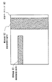
図4は、検査データの1領域を示す図である。
従来の検査データにおいては、パターン機能の区別がなされていなかった。これに対し、本発明の実施の形態では、例えば、図4のように、検査データの1領域である検査データエリア60内において、信号配線61には検査感度区分番号1が、電源配線62には検査感度区分番号2が付加されて区別される。
【0037】
次に、パターン機能ごとに付加された検査感度区分番号に対応した検査感度が、検査感度設定部32において割り当てられる。この設定は、例えば、検査条件の設定時に、ユーザより、パターン機能ごとに要求する検査感度を入力するようにしてもよい。この際、検査感度設定部32は、入力された検査感度を検査感度区分番号に対応付けるようにする。
【0038】
一方、被検査対象50は、ステージ40aに設置されており、検査/駆動制御部40の制御のもと、ステージスキャンされ、被検査対象50の所定の位置におけるパターンが画像取得部33において撮像される。さらに、信号処理によってデジタルの被検査データに変換される。
【0039】
さらに、検査データ及び被検査データは、それぞれ、画像変換部34、35で画像変換が行われ、比較判断部36で画像データの比較が行われる。この比較の際、検査感度設定部32で設定された検査感度を参照して、例えば、図4のような複数の異なる検査感度区分番号が付加されたパターン機能が検査データエリア60内に存在する場合には、検査感度が最小のものを採用して、欠陥を検出する。
【0040】
図5は、検出された欠陥の例である。
これは、画像変換後、比較判断部36で、図4で示された検査データエリア60の検査データと比較して検出された被検査対象50(ここではレチクルとする)の欠陥の例である。
【0041】
図5のように、例えば、レーザなどによる遮光膜の昇華によって発生するピンホールPh1、Ph2、Ph3及び、エッチング時に所望の場所以外に遮光膜のクロムが残った部分であるクロム残Cr1、Cr2、Cr3といった欠陥が検出される。
【0042】
比較判断部36では、さらに、欠陥検出時に、検出された欠陥のパターン重心座標と欠陥サイズを検出し、欠陥パターンエリアを算出する。
図6は、欠陥パターンエリア算出方法を説明する図である。
【0043】
ここでは、図5で示したクロム残Cr3について、欠陥パターンエリアの算出方法を説明する。
欠陥の検出時には、X−Y座標で示された、欠陥サイズと、パターン重心座標が検出される。例えば、図のようにX方向の大きさであるXサイズは4.5μm、Y方向の大きさであるYサイズは2.5μm、パターン重心座標は、X:5047.750μm、Y:179.500μmなどと算出される。さらに、これらより、図6のA、Bの対角で示される領域からなる欠陥パターンエリア70が算出される。
【0044】
ここで、検査データのフォーマットを説明する。
図7は、検査データエリアを示す図である。
検査データは、図のように、X方向のセグメント番号と、Y方向のストライプ番号で表される複数のデータエリアから構成されている。
【0045】
検査データ抽出部37では、図7のように表される検査データより、例えば、図6で示した欠陥パターンエリア70が属するデータエリアを抽出する。
例えば、図6のA及びBの座標は、欠陥サイズと、パターン重心座標から算出されるので、これらを検査データの単位セグメント及び単位ストライプの長さで割ることで、欠陥パターンエリア70が検査データ内で属するデータエリアを算出できる。ここで、算出された検査データのデータエリアを抽出する。例えば、図6で示したクロム残Cr3の欠陥パターンエリア70が、セグメント番号4、ストライプ番号4の検査データエリア60に属すると算出された場合は、図7において、検査データエリア60が抽出される。
【0046】
次に、欠陥登録判定部38の動作を説明する。
欠陥登録判定部38では、まず、検査データ抽出部37で抽出された検査データエリア60をもとに、欠陥判定範囲を作成する。
【0047】
図8は、欠陥判定範囲の作成方法を説明する図である。
抽出された検査データエリア60において、検査感度区分番号で区分されたパターン機能に所定量のシフト処理を行ない、欠陥判定範囲を作成する。図8は、パターン機能に1μmのシフトをかけた場合のものであり、検査感度区分番号1の信号配線61からなる欠陥判定範囲81と、検査感度区分番号2の電源配線62からなる欠陥判定範囲82とが形成される。
【0048】
次に、前述の図6のようにして、決定された欠陥パターンエリア70を、欠陥判定範囲81、82と合成する。
図9は、欠陥判定範囲と欠陥パターンエリアとを合成した図である。
【0049】
図9では、欠陥判定範囲81、82の両方に、欠陥パターンエリア70が重なり合っている場合について示した。欠陥判定の際、欠陥判定範囲81、82と、欠陥パターンエリア70との重なり部分を調べるため、AND処理を行なう。まず、高い検査感度が割り当てられた検査感度区分番号1の欠陥判定範囲81と、欠陥パターンエリア70とのAND処理を優先的に行ない、その結果が1の場合、欠陥パターンエリア70で示される欠陥は検査感度区分番号1の欠陥判定範囲に属する欠陥として登録される。一方、図9では欠陥パターンエリア70は欠陥判定範囲81、82の両方と重なっているが、例えば、欠陥判定範囲81との重なりがない場合、すなわち、AND処理の結果が0の場合、続いて、検査感度区分番号2の欠陥判定範囲82と、欠陥パターンエリア70とのAND処理を行なう。ここで、その結果が1の場合、欠陥パターンエリア70で示される欠陥は検査感度区分番号2の欠陥判定範囲に属する欠陥とする。ただしこの際、欠陥のサイズと、検査感度区分番号2に割り当てられた検査感度を参照して、欠陥のサイズが検査感度より小さい欠陥の場合は、欠陥として登録しない。
【0050】
以下、図5における各欠陥における欠陥判定を説明する。
図10は、図5で示した欠陥と、欠陥判定範囲及びパターン機能を合成した様子を示す図である。
【0051】
ここで、ピンホールPh1のサイズが0.5μm、ピンホールPh2は0.8μm、ピンホールPh3は1.0μm、クロム残Cr1のサイズが1.0μm、クロム残Cr2は0.9μm、クロム残Cr3は4.5μmであるとする。
【0052】
さらに、検査感度区分番号1には検査感度0.5μm、検査感度区分番号2には検査感度1.0μmが割り当てられているとして説明する。
ここで、ピンホールPh1は、検査感度区分番号1の欠陥判定範囲81のみに属する欠陥で、欠陥サイズが0.5μmであり、検査感度区分番号1に割り当てられた検査感度以上であるので、欠陥として登録する。
【0053】
ピンホールPh2は、検査感度区分番号2の欠陥判定範囲82のみに属する欠陥であるが、欠陥サイズが0.8μmであり、検査感度区分番号2に割り当てられた検査感度1.0μmより小さい欠陥であるので、欠陥として登録しない。
【0054】
また、ピンホールPh3は、検査感度区分番号2の欠陥判定範囲82のみに属する欠陥で、欠陥サイズが1.0μmであり、検査感度区分番号2に割り当てられた検査感度以上であるので、欠陥として登録する。
【0055】
一方、クロム残Cr1は、どちらの欠陥判定範囲81、82にも属さない欠陥であるので、欠陥として登録しない。
クロム残Cr2は、検査感度区分番号2の欠陥判定範囲82のみに属する欠陥であるが、欠陥サイズが0.9μmであり、検査感度区分番号2に割り当てられた検査感度1.0μmより小さい欠陥であるので、欠陥として登録しない。
【0056】
クロム残Cr3は、前述したが、検査感度区分番号1、2の欠陥判定範囲81、82の両方に属する欠陥であるので、より高い検査感度が割り当てられた検査感度区分番号1を優先して、欠陥として登録する。
【0057】
なお、上記では、欠陥判定範囲81、82に属さない欠陥を、登録しないようにしたが、パターン機能以外の部分にも、検査感度区分番号を付加し、検査感度を割り当てるようにしてもよい。その場合、例えば、クロム残Cr1は、割り当てられた検査感度を参照して、その検査感度以上の大きさであれば、欠陥として登録する。
【0058】
上記のようにして、欠陥登録判定部38で欠陥として判定された欠陥は、欠陥記憶部39に記憶される。
次に、前述した検査装置30での検査方法をフローチャートを用いて説明する。
【0059】
図11は、検査方法を示すフローチャートである。
S10:検査データ生成
設計データのパターン機能ごとに、検査感度で区分するための検査感度区分情報を含めた検査データを生成する。
【0060】
S11:被検査対象セット
検査装置30のステージ40aに被検査対象50であるフォトマスクやウェハーをセットする。
【0061】
S12:検査感度設定
検査感度区分情報に、所望の検査感度を割り当てる。
S13:ステージスキャン
検査/駆動制御部40の制御のもと、ステージ40aを駆動させて、被検査対象50の所定の位置から検査を開始する。
【0062】
S14:実パターン取り込み
画像取得部33により、被検査対象50であるフォトマスクやウェハーの実パターンを画像として取り込み、デジタルデータに変換し、被検査データを生成する。
【0063】
S15:被検査データ画像変換
検査データとの画像データの比較のために、被検査データを画像変換する。
S16:検査データの取り込み
取り込んだ実パターンに対応する検査データを取り込む。
【0064】
S17:検査データ画像変換
被検査データとの画像データの比較のために、検査データを画像変換する。
S18:画像データ比較
比較判断部36で被検査データと、検査データの比較が行われる。この比較の際、ステップS12で設定された検査感度を参照して、検査領域である検査データ内に、例えば図4のような複数の異なる検査感度区分番号が付加されたパターン機能が存在する場合には、検査感度が最小のものを採用して、欠陥を検出する。
【0065】
S19:欠陥が検出されたか否かの判断
ステップS18における、画像データの比較で、欠陥が検出されたか否かの判断を行なう。ここで欠陥が検出されなければ、ステップS20に進み、欠陥が検出されたと判断されればステップS21に進む。
【0066】
S20:スキャンが終了したか否かの判断
検査/駆動制御部40の制御のもと、被検査対象50のステージスキャンが終了したか否かを判断し、スキャンが終了したと判断された場合、被検査対象50の検査は終了となり処理を終了する。また、スキャンがまだ終了していない場合は、ステップS13に戻る。
【0067】
S21:検査データ抽出
図7のように表される検査データより、図6で示したような欠陥パターンエリア70が属するデータエリアを抽出する。
【0068】
S22:欠陥判定範囲算出
図8で示したように、検査感度区分情報で区分されたパターン機能にシフト処理を行ない、欠陥判定範囲を作成する。
【0069】
S23:欠陥範囲判定
図9で示したように、例えば、欠陥パターンエリア70と、欠陥判定範囲81、82とを合成して、欠陥パターンエリア70が、どの欠陥判定範囲81、82に属する欠陥か判定する。
【0070】
S24:優先度判定
ここでは、例えば、図9のように欠陥パターンエリア70が複数の欠陥判定範囲81、82に属する場合、パターン機能の検査感度区分情報に割り当てられた検査感度を参照して、その優先度を判定する。
【0071】
S25:欠陥を登録するか否かの判断
ステップS24での優先度に従って、優先する欠陥判定範囲81、82を決定し、その検査感度区分情報に対応付けられている検査感度を参照して、欠陥を登録するか否かを判断する。ここで、欠陥を登録する場合は、ステップS26に進み、欠陥を登録しない場合は、ステップS20に戻る。
【0072】
S26:欠陥記憶
ステップS25で、検出した欠陥を登録すると判定されたのを受けて、検出した欠陥を欠陥記憶部39に記憶させる。その後ステップS20に戻る。
【0073】
このようにして、検査データに、パターン機能を検査感度で区別するための、検査感度区分情報を付加し、検査感度区分情報に検査感度を割り当てることで、パターン機能に応じた検査感度で検査を行うことができる。
【0074】
【発明の効果】
以上説明したように本発明では、検査データ内の所定のパターンが有するパターン機能ごとに、検査感度区分情報をもたせることで、クロック信号線、アドレス信号線、データ入出力信号線、制御信号線、または電源線といったパターン機能を区別することができる。また、検査感度区分情報に所望の検査感度を設定して、検査感度に応じて欠陥登録の判定を行うことにより、性能に影響されない欠陥の登録を抑えられる。これにより、性能に影響されない欠陥の修正時間を不要とするため、検査から修正までのトータル的な時間短縮が可能となる。
【図面の簡単な説明】
【図1】本発明の実施の形態の検査装置の概略の構成を示すブロック図である。
【図2】検査方法を示すフローチャートである。
【図3】本発明の実施の形態の検査装置の構成を示すブロック図である。
【図4】検査データの1領域を示す図である。
【図5】検出された欠陥の例である。
【図6】欠陥パターンエリア算出方法を説明する図である。
【図7】検査データエリアを示す図である。
【図8】欠陥判定範囲の作成方法を説明する図である。
【図9】欠陥判定範囲と欠陥パターンエリアとを合成した図である。
【図10】 図5で示した欠陥と、欠陥判定範囲及びパターン機能を合成した様子を示す図である。
【図11】検査方法を示すフローチャートである。
【図12】従来の検査装置の構成を示すブロック図である。
【符号の説明】
10 検査装置
11 検査データ生成部
12 検査感度設定部
13 画像取得部
14 比較判断部
15 検査データ抽出部
16 欠陥登録判定部
17 欠陥記憶部
20 被検査対象[0001]
BACKGROUND OF THE INVENTION
The present invention relates to an inspection apparatus and an inspection method, and more particularly to an inspection apparatus and an inspection method for inspecting a photomask or a wafer.
[0002]
[Prior art]
With the progress of miniaturization of LSI (Large-Scale Integrated circuit), in recent years, not only wafers but also the accuracy of photomasks such as reticles used for LSI production are increasing.
[0003]
On the other hand, improvement in inspection sensitivity is also required for inspection apparatuses that detect defects in photomasks and wafers.
FIG. 12 is a block diagram showing a configuration of a conventional inspection apparatus.
[0004]
The
[0005]
In this
[0006]
As described above, the
[0007]
[Problems to be solved by the invention]
However, in the
[0008]
The present invention has been made in view of these points, and an object thereof is to provide an inspection apparatus capable of shortening the time from inspection to correction.
Another object of the present invention is to provide an inspection method capable of shortening the time from inspection to correction.
[0009]
[Means for Solving the Problems]
In the present invention, in order to solve the above-mentioned problem, in an
[0010]
According to the above configuration, the pattern functions are distinguished by the inspection sensitivity classification information, and the inspection sensitivity is set for each pattern function.
[0011]
DETAILED DESCRIPTION OF THE INVENTION
Embodiments of the present invention will be described below with reference to the drawings.
FIG. 1 is a block diagram showing a schematic configuration of an inspection apparatus according to an embodiment of the present invention.
[0012]
The
[0013]
The inspection
[0014]
The inspection
[0015]
The
The
[0016]
The inspection
The defect
[0017]
The
Hereinafter, the operation of the
When design data corresponding to the
[0018]
Hereinafter, an outline of an inspection method in the
FIG. 2 is a flowchart showing the inspection method.
[0019]
S1: Generation of inspection data
Based on the design data, the inspection
[0020]
S2: Setting of inspection sensitivity
An inspection sensitivity is assigned for each inspection sensitivity classification information of inspection data.
S3: Image data generated by inspecting photomask or wafer
In the
[0021]
S4: Comparison between inspection data and inspection data
The inspection data and the data to be inspected are compared by the comparison /
[0022]
S5: Determination of whether or not a defect has been detected
From the comparison between the inspection data in step S4 and the data to be inspected, if a defect is detected, the process proceeds to step S6, and if no defect is detected, the process is terminated.
[0023]
S6: Extraction of the area in the inspection data where the detected defect exists
The inspection
[0024]
S7: Determination of whether or not to register a defect
In the region in the inspection data extracted in step S6, the defect
[0025]
If it is determined to register as a defect, the process proceeds to step S8. If it is determined not to register, the process ends.
S8: Defect memory
The defect determined to be registered in step S7 is stored in the defect storage unit.
[0026]
As described above, the pattern functions can be distinguished by providing inspection sensitivity classification information for each pattern function in the inspection data. Further, by setting a desired inspection sensitivity in the inspection sensitivity classification information and performing defect registration determination according to the inspection sensitivity, it is possible to suppress registration of defects that are not affected by performance. This eliminates the need for a defect correction time that is not affected by the performance, thereby reducing the total time from inspection to correction.
[0027]
Hereinafter, details of the inspection apparatus and the inspection method according to the embodiment of the present invention will be described.
FIG. 3 is a block diagram showing the configuration of the inspection apparatus according to the embodiment of the present invention.
The
[0028]
The inspection
[0029]
The inspection
At this time, the highest inspection sensitivity is assigned to the inspection sensitivity classification information added to the clock signal line, the lowest inspection sensitivity is assigned to the inspection sensitivity classification information added to the power supply line, and the other signal lines are at the same level. It is desirable to assign the inspection sensitivity. Specifically, when numbers are used as inspection sensitivity classification information, inspection
[0030]
The
[0031]
The
The
[0032]
The inspection
In the extracted inspection data area, the defect
[0033]
The
[0034]
Hereinafter, the operation of the
For example, when design data of an
[0035]
In the inspection data, inspection sensitivity classification information for classification by inspection sensitivity is added for each pattern function described in the design data. Hereinafter, a case where numbers are applied as the inspection sensitivity classification information will be described. In this case, the inspection sensitivity classification information is referred to as inspection sensitivity classification number.
[0036]
FIG. 4 is a diagram showing one region of inspection data.
In the conventional inspection data, the pattern function is not distinguished. In contrast, in the embodiment of the present invention, for example, as shown in FIG. 4, the inspection
[0037]
Next, inspection sensitivity corresponding to the inspection sensitivity classification number added for each pattern function is assigned by the inspection
[0038]
On the other hand, the
[0039]
Further, the inspection data and the data to be inspected are subjected to image conversion by the
[0040]
FIG. 5 is an example of a detected defect.
This is an example of the defect of the inspection object 50 (here, a reticle) detected by the comparison /
[0041]
As shown in FIG. 5, for example, pinholes Ph1, Ph2, and Ph3 generated by sublimation of the light shielding film by a laser or the like, and chromium remaining Cr1, Cr2, which are portions where the chromium of the light shielding film remains in a desired place other than a desired place during etching, A defect such as Cr3 is detected.
[0042]
The
FIG. 6 is a diagram for explaining a defect pattern area calculation method.
[0043]
Here, a method for calculating the defect pattern area for the chromium residual Cr3 shown in FIG. 5 will be described.
When a defect is detected, the defect size and the pattern barycentric coordinates indicated by the XY coordinates are detected. For example, as shown in the figure, the X size that is the size in the X direction is 4.5 μm, the Y size that is the size in the Y direction is 2.5 μm, and the pattern barycentric coordinates are X: 5047.750 μm, Y: 179.500 μm. And so on. Further, from these, a
[0044]
Here, the format of the inspection data will be described.
FIG. 7 is a diagram showing an inspection data area.
As shown in the figure, the inspection data is composed of a plurality of data areas represented by segment numbers in the X direction and stripe numbers in the Y direction.
[0045]
The inspection
For example, the coordinates of A and B in FIG. 6 are calculated from the defect size and the pattern barycentric coordinates. By dividing these by the length of the unit segment and unit stripe of the inspection data, the
[0046]
Next, the operation of the defect
The defect
[0047]
FIG. 8 is a diagram illustrating a method for creating a defect determination range.
In the extracted
[0048]
Next, as shown in FIG. 6 described above, the determined
FIG. 9 is a diagram in which the defect determination range and the defect pattern area are combined.
[0049]
FIG. 9 shows a case where the
[0050]
Hereinafter, the defect determination for each defect in FIG. 5 will be described.
FIG. 5 The defect shown in, and the defect determination range and pattern function were synthesized Diagram showing the situation It is.
[0051]
Here, the size of the pinhole Ph1 is 0.5 μm, the pinhole Ph2 is 0.8 μm, the pinhole Ph3 is 1.0 μm, the size of the chromium residual Cr1 is 1.0 μm, the chromium residual Cr2 is 0.9 μm, and the chromium residual Cr3 Is 4.5 μm.
[0052]
Further, it is assumed that inspection sensitivity 0.5 is assigned to inspection
Here, the pinhole Ph1 is a defect that belongs only to the
[0053]
The pinhole Ph2 is a defect that belongs only to the
[0054]
Further, the pinhole Ph3 is a defect that belongs only to the
[0055]
On the other hand, the chromium residual Cr1 is not registered as a defect because it is a defect that does not belong to any
The chromium residual Cr2 is a defect that belongs only to the
[0056]
As described above, the chromium residual Cr3 is a defect belonging to both of the defect determination ranges 81 and 82 of the inspection
[0057]
In the above description, defects that do not belong to the defect determination ranges 81 and 82 are not registered, but inspection sensitivity classification numbers may be added to portions other than the pattern function to assign inspection sensitivity. In this case, for example, the chromium residual Cr1 is registered as a defect if it is larger than the inspection sensitivity with reference to the assigned inspection sensitivity.
[0058]
The defects determined as defects by the defect
Next, the inspection method in the above-described
[0059]
FIG. 11 is a flowchart showing the inspection method.
S10: Inspection data generation
Inspection data including inspection sensitivity classification information for classification by inspection sensitivity is generated for each pattern function of the design data.
[0060]
S11: Inspection target set
A photomask or wafer that is the
[0061]
S12: Inspection sensitivity setting
A desired inspection sensitivity is assigned to the inspection sensitivity classification information.
S13: Stage scan
Under the control of the inspection /
[0062]
S14: Capture actual pattern
The
[0063]
S15: Inspection data image conversion
The data to be inspected is converted into an image for comparison of the image data with the inspection data.
S16: Import inspection data
The inspection data corresponding to the acquired actual pattern is acquired.
[0064]
S17: Inspection data image conversion
In order to compare the image data with the data to be inspected, the inspection data is converted into an image.
S18: Image data comparison
The
[0065]
S19: Determination of whether or not a defect has been detected
In step S18, it is determined whether or not a defect has been detected by comparing the image data. If no defect is detected, the process proceeds to step S20. If it is determined that a defect is detected, the process proceeds to step S21.
[0066]
S20: Judgment whether or not scanning is completed
Under the control of the inspection /
[0067]
S21: Inspection data extraction
A data area to which the
[0068]
S22: Defect determination range calculation
As shown in FIG. 8, a shift process is performed on the pattern function divided by the inspection sensitivity classification information to create a defect determination range.
[0069]
S23: Defect range determination
As shown in FIG. 9, for example, the
[0070]
S24: Priority determination
Here, for example, when the
[0071]
S25: Determination of whether or not to register a defect
In accordance with the priority in step S24, the defect determination ranges 81 and 82 to be prioritized are determined, and it is determined whether or not to register a defect with reference to the inspection sensitivity associated with the inspection sensitivity classification information. Here, when registering a defect, it progresses to step S26, and when not registering a defect, it returns to step S20.
[0072]
S26: Defect memory
In step S25, in response to the determination that the detected defect is registered, the detected defect is stored in the
[0073]
In this way, inspection sensitivity classification information for distinguishing pattern functions by inspection sensitivity is added to inspection data, and inspection sensitivity is assigned to inspection sensitivity classification information, so that inspection can be performed with inspection sensitivity according to the pattern function. It can be carried out.
[0074]
【The invention's effect】
As described above, in the present invention, by providing inspection sensitivity classification information for each pattern function of a predetermined pattern in inspection data, Clock signal line, address signal line, data input / output signal line, control signal line, power supply line, etc. The pattern function can be distinguished. Further, by setting a desired inspection sensitivity in the inspection sensitivity classification information and performing defect registration determination according to the inspection sensitivity, it is possible to suppress registration of defects that are not affected by performance. This eliminates the need for a defect correction time that is not affected by the performance, thereby reducing the total time from inspection to correction.
[Brief description of the drawings]
FIG. 1 is a block diagram showing a schematic configuration of an inspection apparatus according to an embodiment of the present invention.
FIG. 2 is a flowchart showing an inspection method.
FIG. 3 is a block diagram showing a configuration of the inspection apparatus according to the embodiment of the present invention.
FIG. 4 is a diagram showing one region of inspection data.
FIG. 5 is an example of a detected defect.
FIG. 6 is a diagram illustrating a defect pattern area calculation method.
FIG. 7 is a diagram showing an inspection data area.
FIG. 8 is a diagram illustrating a method for creating a defect determination range.
FIG. 9 is a diagram in which a defect determination range and a defect pattern area are synthesized.
FIG. 10 5 It is a figure which shows a mode that the defect shown by (3), the defect determination range, and the pattern function were synthesize | combined.
FIG. 11 is a flowchart showing an inspection method.
FIG. 12 is a block diagram showing a configuration of a conventional inspection apparatus.
[Explanation of symbols]
10 Inspection equipment
11 Inspection data generator
12 Inspection sensitivity setting section
13 Image acquisition unit
14 Comparison judgment part
15 Inspection data extraction unit
16 Defect registration determination unit
17 Defect storage
20 Inspected
Claims (10)
設計データをもとに、所定のパターンが有するクロック信号線、アドレス信号線、データ入出力信号線、制御信号線、または電源線のいずれかを含むパターン機能を、検査感度で区分する検査感度区分情報を含む、検査データを生成する検査データ生成部と、
前記検査感度区分情報ごとに、所望の検査感度を割り当てる検査感度設定部と、
前記フォトマスクまたはウェハーを撮像して、被検査データを生成する画像取得部と、
前記被検査データと、前記検査データとを比較し、欠陥を検出する比較判断部と、
検出された前記欠陥が存在する、前記検査データ内の領域を抽出する検査データ抽出部と、
前記領域に含まれるパターンに対して設定された前記検査感度区分情報を参照し、前記欠陥を登録するか否かを判定する欠陥登録判定部と、
登録すると判定された前記欠陥を記憶する欠陥記憶部と、
を有することを特徴とする検査装置。In inspection equipment for inspecting photomasks or wafers,
Based on the design data, a clock signal line having a predetermined pattern, the address signal lines, the data input and output signal lines, control signal lines or a pattern functions including any of the power line, inspection sensitivity classification for distinguishing the inspection sensitivity An inspection data generation unit for generating inspection data including information;
An inspection sensitivity setting unit that assigns a desired inspection sensitivity for each inspection sensitivity classification information,
An image acquisition unit that images the photomask or wafer and generates data to be inspected;
A comparison judgment unit that compares the inspection data with the inspection data and detects a defect;
An inspection data extraction unit for extracting an area in the inspection data where the detected defect exists;
A defect registration determination unit that determines whether or not to register the defect with reference to the inspection sensitivity classification information set for the pattern included in the region;
A defect memory unit that stores the defect is determined to be registered,
An inspection apparatus comprising:
設計データをもとに、所定のパターンが有するクロック信号線、アドレス信号線、データ入出力信号線、制御信号線、または電源線のいずれかを含むパターン機能を、検査感度で区分する検査感度区分情報を含む検査データを生成し、
前記検査感度区分情報ごとに、所望の検査感度を割り当て、
前記フォトマスクまたはウェハーを撮像して被検査データを生成し、
前記被検査データと、前記検査データとを比較して欠陥を検出し、
検出された前記欠陥が存在する、前記検査データ内の領域を抽出し、
前記領域に含まれるパターンに対して設定された前記検査感度区分情報を参照して、前記欠陥を登録するか否かを判定し、
登録すると判定された前記欠陥を記憶することを特徴とする検査方法。In an inspection method for inspecting a photomask or wafer,
Based on the design data, a clock signal line having a predetermined pattern, the address signal lines, the data input and output signal lines, control signal lines or a pattern functions including any of the power line, inspection sensitivity classification for distinguishing the inspection sensitivity Generate inspection data including information,
For each inspection sensitivity category information, assign a desired inspection sensitivity,
Imaging the photomask or wafer to generate inspection data,
Detecting the defect by comparing the inspection data and the inspection data;
Extracting an area in the inspection data where the detected defect exists;
With reference to the inspection sensitivity classification information set for the pattern included in the region, determine whether to register the defect,
An inspection method characterized by storing the defect determined to be registered.
Priority Applications (2)
| Application Number | Priority Date | Filing Date | Title |
|---|---|---|---|
| JP2002199595A JP4073265B2 (en) | 2002-07-09 | 2002-07-09 | Inspection apparatus and inspection method |
| US10/607,039 US7424145B2 (en) | 2002-07-09 | 2003-06-27 | Device and method for inspecting photomasks and products fabricated using the same |
Applications Claiming Priority (1)
| Application Number | Priority Date | Filing Date | Title |
|---|---|---|---|
| JP2002199595A JP4073265B2 (en) | 2002-07-09 | 2002-07-09 | Inspection apparatus and inspection method |
Publications (2)
| Publication Number | Publication Date |
|---|---|
| JP2004045066A JP2004045066A (en) | 2004-02-12 |
| JP4073265B2 true JP4073265B2 (en) | 2008-04-09 |
Family
ID=30112473
Family Applications (1)
| Application Number | Title | Priority Date | Filing Date |
|---|---|---|---|
| JP2002199595A Expired - Fee Related JP4073265B2 (en) | 2002-07-09 | 2002-07-09 | Inspection apparatus and inspection method |
Country Status (2)
| Country | Link |
|---|---|
| US (1) | US7424145B2 (en) |
| JP (1) | JP4073265B2 (en) |
Families Citing this family (69)
| Publication number | Priority date | Publication date | Assignee | Title |
|---|---|---|---|---|
| US7698665B2 (en) * | 2003-04-06 | 2010-04-13 | Luminescent Technologies, Inc. | Systems, masks, and methods for manufacturable masks using a functional representation of polygon pattern |
| US7124394B1 (en) * | 2003-04-06 | 2006-10-17 | Luminescent Technologies, Inc. | Method for time-evolving rectilinear contours representing photo masks |
| US9002497B2 (en) | 2003-07-03 | 2015-04-07 | Kla-Tencor Technologies Corp. | Methods and systems for inspection of wafers and reticles using designer intent data |
| US7135344B2 (en) * | 2003-07-11 | 2006-11-14 | Applied Materials, Israel, Ltd. | Design-based monitoring |
| US7234128B2 (en) * | 2003-10-03 | 2007-06-19 | Taiwan Semiconductor Manufacturing Company, Ltd. | Method for improving the critical dimension uniformity of patterned features on wafers |
| JP2005158780A (en) | 2003-11-20 | 2005-06-16 | Hitachi Ltd | Method and device for inspecting defect of pattern |
| US7646906B2 (en) | 2004-01-29 | 2010-01-12 | Kla-Tencor Technologies Corp. | Computer-implemented methods for detecting defects in reticle design data |
| JP4904034B2 (en) | 2004-09-14 | 2012-03-28 | ケーエルエー−テンカー コーポレイション | Method, system and carrier medium for evaluating reticle layout data |
| JP2006170922A (en) * | 2004-12-20 | 2006-06-29 | Topcon Corp | Visual inspection method and its apparatus |
| JP4954469B2 (en) * | 2004-12-20 | 2012-06-13 | 株式会社トプコン | Appearance inspection method |
| JP4644210B2 (en) | 2005-01-14 | 2011-03-02 | 富士通セミコンダクター株式会社 | Pattern defect inspection method |
| US7769225B2 (en) | 2005-08-02 | 2010-08-03 | Kla-Tencor Technologies Corp. | Methods and systems for detecting defects in a reticle design pattern |
| JP4185515B2 (en) * | 2005-08-29 | 2008-11-26 | アドバンスド・マスク・インスペクション・テクノロジー株式会社 | Sample inspection method, program, and sample inspection apparatus |
| KR101330344B1 (en) * | 2005-09-13 | 2013-11-15 | 루미네슨트 테크놀로지, 인크. | Systems, masks, and methods for photolithography |
| JP4738114B2 (en) * | 2005-09-16 | 2011-08-03 | 株式会社東芝 | Mask defect inspection method |
| WO2007041600A2 (en) * | 2005-10-03 | 2007-04-12 | Luminescent Technologies, Inc. | Mask-pattern determination using topology types |
| WO2007041602A2 (en) * | 2005-10-03 | 2007-04-12 | Luminescent Technologies, Inc. | Lithography verification using guard bands |
| US7793253B2 (en) * | 2005-10-04 | 2010-09-07 | Luminescent Technologies, Inc. | Mask-patterns including intentional breaks |
| WO2007044557A2 (en) | 2005-10-06 | 2007-04-19 | Luminescent Technologies, Inc. | System, masks, and methods for photomasks optimized with approximate and accurate merit functions |
| US8041103B2 (en) | 2005-11-18 | 2011-10-18 | Kla-Tencor Technologies Corp. | Methods and systems for determining a position of inspection data in design data space |
| US7676077B2 (en) | 2005-11-18 | 2010-03-09 | Kla-Tencor Technologies Corp. | Methods and systems for utilizing design data in combination with inspection data |
| KR101613048B1 (en) * | 2005-11-18 | 2016-04-15 | 케이엘에이-텐코 코포레이션 | Methods and systems for utilizing design data in combination with inspection data |
| US7570796B2 (en) | 2005-11-18 | 2009-08-04 | Kla-Tencor Technologies Corp. | Methods and systems for utilizing design data in combination with inspection data |
| US8331645B2 (en) * | 2006-09-20 | 2012-12-11 | Luminescent Technologies, Inc. | Photo-mask and wafer image reconstruction |
| WO2008039674A2 (en) * | 2006-09-20 | 2008-04-03 | Luminescent Technologies, Inc. | Photo-mask and wafer image reconstruction |
| WO2008077100A2 (en) | 2006-12-19 | 2008-06-26 | Kla-Tencor Corporation | Systems and methods for creating inspection recipes |
| US8194968B2 (en) | 2007-01-05 | 2012-06-05 | Kla-Tencor Corp. | Methods and systems for using electrical information for a device being fabricated on a wafer to perform one or more defect-related functions |
| US7738093B2 (en) * | 2007-05-07 | 2010-06-15 | Kla-Tencor Corp. | Methods for detecting and classifying defects on a reticle |
| US7962863B2 (en) | 2007-05-07 | 2011-06-14 | Kla-Tencor Corp. | Computer-implemented methods, systems, and computer-readable media for determining a model for predicting printability of reticle features on a wafer |
| US8213704B2 (en) | 2007-05-09 | 2012-07-03 | Kla-Tencor Corp. | Methods and systems for detecting defects in a reticle design pattern |
| US7796804B2 (en) | 2007-07-20 | 2010-09-14 | Kla-Tencor Corp. | Methods for generating a standard reference die for use in a die to standard reference die inspection and methods for inspecting a wafer |
| US7711514B2 (en) | 2007-08-10 | 2010-05-04 | Kla-Tencor Technologies Corp. | Computer-implemented methods, carrier media, and systems for generating a metrology sampling plan |
| US7975245B2 (en) | 2007-08-20 | 2011-07-05 | Kla-Tencor Corp. | Computer-implemented methods for determining if actual defects are potentially systematic defects or potentially random defects |
| JP2009071136A (en) * | 2007-09-14 | 2009-04-02 | Hitachi High-Technologies Corp | Data management device, inspection system and defect reviewing apparatus |
| JP4870704B2 (en) * | 2008-03-21 | 2012-02-08 | 株式会社ニューフレアテクノロジー | Pattern inspection apparatus and pattern inspection method |
| US8139844B2 (en) | 2008-04-14 | 2012-03-20 | Kla-Tencor Corp. | Methods and systems for determining a defect criticality index for defects on wafers |
| KR101841897B1 (en) | 2008-07-28 | 2018-03-23 | 케이엘에이-텐코어 코오포레이션 | Computer-implemented methods, computer-readable media, and systems for classifying defects detected in a memory device area on a wafer |
| US8775101B2 (en) | 2009-02-13 | 2014-07-08 | Kla-Tencor Corp. | Detecting defects on a wafer |
| US8204297B1 (en) | 2009-02-27 | 2012-06-19 | Kla-Tencor Corp. | Methods and systems for classifying defects detected on a reticle |
| US8112241B2 (en) * | 2009-03-13 | 2012-02-07 | Kla-Tencor Corp. | Methods and systems for generating an inspection process for a wafer |
| JP4933601B2 (en) | 2009-08-18 | 2012-05-16 | 株式会社ニューフレアテクノロジー | Inspection apparatus and inspection method |
| US8797721B2 (en) | 2010-02-02 | 2014-08-05 | Apple Inc. | Portable electronic device housing with outer glass surfaces |
| US8463016B2 (en) * | 2010-02-05 | 2013-06-11 | Luminescent Technologies, Inc. | Extending the field of view of a mask-inspection image |
| US8781781B2 (en) | 2010-07-30 | 2014-07-15 | Kla-Tencor Corp. | Dynamic care areas |
| US8555214B2 (en) | 2010-09-14 | 2013-10-08 | Luminescent Technologies, Inc. | Technique for analyzing a reflective photo-mask |
| US8612903B2 (en) | 2010-09-14 | 2013-12-17 | Luminescent Technologies, Inc. | Technique for repairing a reflective photo-mask |
| US8386968B2 (en) | 2010-11-29 | 2013-02-26 | Luminescent Technologies, Inc. | Virtual photo-mask critical-dimension measurement |
| US8458622B2 (en) | 2010-11-29 | 2013-06-04 | Luminescent Technologies, Inc. | Photo-mask acceptance technique |
| US9005852B2 (en) | 2012-09-10 | 2015-04-14 | Dino Technology Acquisition Llc | Technique for repairing a reflective photo-mask |
| US9170211B2 (en) | 2011-03-25 | 2015-10-27 | Kla-Tencor Corp. | Design-based inspection using repeating structures |
| US9087367B2 (en) | 2011-09-13 | 2015-07-21 | Kla-Tencor Corp. | Determining design coordinates for wafer defects |
| US8831334B2 (en) | 2012-01-20 | 2014-09-09 | Kla-Tencor Corp. | Segmentation for wafer inspection |
| JP6184473B2 (en) * | 2012-03-20 | 2017-08-23 | ケーエルエー−テンカー コーポレイション | Using reflection and transmission maps to detect reticle degradation |
| US9858658B2 (en) | 2012-04-19 | 2018-01-02 | Applied Materials Israel Ltd | Defect classification using CAD-based context attributes |
| US9595091B2 (en) * | 2012-04-19 | 2017-03-14 | Applied Materials Israel, Ltd. | Defect classification using topographical attributes |
| US9207070B2 (en) * | 2012-05-24 | 2015-12-08 | Qualcomm Incorporated | Transmission of affine-invariant spatial mask for active depth sensing |
| US8826200B2 (en) | 2012-05-25 | 2014-09-02 | Kla-Tencor Corp. | Alteration for wafer inspection |
| US9189844B2 (en) | 2012-10-15 | 2015-11-17 | Kla-Tencor Corp. | Detecting defects on a wafer using defect-specific information |
| US9053527B2 (en) | 2013-01-02 | 2015-06-09 | Kla-Tencor Corp. | Detecting defects on a wafer |
| US9134254B2 (en) | 2013-01-07 | 2015-09-15 | Kla-Tencor Corp. | Determining a position of inspection system output in design data space |
| US9311698B2 (en) | 2013-01-09 | 2016-04-12 | Kla-Tencor Corp. | Detecting defects on a wafer using template image matching |
| WO2014149197A1 (en) | 2013-02-01 | 2014-09-25 | Kla-Tencor Corporation | Detecting defects on a wafer using defect-specific and multi-channel information |
| US9091935B2 (en) | 2013-03-11 | 2015-07-28 | Kla-Tencor Corporation | Multistage extreme ultra-violet mask qualification |
| US9494854B2 (en) | 2013-03-14 | 2016-11-15 | Kla-Tencor Corporation | Technique for repairing an EUV photo-mask |
| US9865512B2 (en) | 2013-04-08 | 2018-01-09 | Kla-Tencor Corp. | Dynamic design attributes for wafer inspection |
| US9310320B2 (en) | 2013-04-15 | 2016-04-12 | Kla-Tencor Corp. | Based sampling and binning for yield critical defects |
| IL260417B (en) | 2018-07-04 | 2021-10-31 | Tinyinspektor Ltd | System and method for automated visual inspection |
| IL272752B2 (en) * | 2020-02-13 | 2023-06-01 | Inspekto A M V Ltd | User interface device for autonomous machine vision inspection |
| EP4104100A4 (en) * | 2020-02-13 | 2024-01-10 | Inspekto A M V Ltd | User interface device for autonomous machine vision inspection |
Family Cites Families (12)
| Publication number | Priority date | Publication date | Assignee | Title |
|---|---|---|---|---|
| JPS63225153A (en) * | 1987-03-14 | 1988-09-20 | Omron Tateisi Electronics Co | Method for inspecting substrate |
| JP2000004079A (en) * | 1998-06-12 | 2000-01-07 | Omron Corp | Solder inspection equipment |
| JP2000146857A (en) * | 1998-11-13 | 2000-05-26 | Toshiba Corp | Pattern defect inspection method, and device therefor |
| JP2000346627A (en) * | 1999-06-07 | 2000-12-15 | Toray Eng Co Ltd | Inspection system |
| JP3524819B2 (en) * | 1999-07-07 | 2004-05-10 | 株式会社日立製作所 | Pattern inspection method and apparatus by image comparison |
| US6507944B1 (en) * | 1999-07-30 | 2003-01-14 | Fujitsu Limited | Data processing method and apparatus, reticle mask, exposing method and apparatus, and recording medium |
| US6482557B1 (en) * | 2000-03-24 | 2002-11-19 | Dupont Photomasks, Inc. | Method and apparatus for evaluating the runability of a photomask inspection tool |
| JP2002100660A (en) * | 2000-07-18 | 2002-04-05 | Hitachi Ltd | Defect detecting method, defect observing method and defect detecting apparatus |
| JP2002148779A (en) * | 2000-11-07 | 2002-05-22 | Toshiba Corp | Mask pattern correcting method, photomask, and computer-readable recording medium stored with mask pattern correcting program |
| JP2002162366A (en) * | 2000-11-27 | 2002-06-07 | Hitachi Ltd | Defect inspection method and its system, and defective area detection method for automatic defect classification |
| US6598211B2 (en) * | 2001-03-30 | 2003-07-22 | Intel Corporation | Scaleable approach to extracting bridges from a hierarchically described VLSI layout |
| JP4104840B2 (en) * | 2001-08-23 | 2008-06-18 | 株式会社東芝 | Mask pattern evaluation system and method |
-
2002
- 2002-07-09 JP JP2002199595A patent/JP4073265B2/en not_active Expired - Fee Related
-
2003
- 2003-06-27 US US10/607,039 patent/US7424145B2/en not_active Expired - Fee Related
Also Published As
| Publication number | Publication date |
|---|---|
| US7424145B2 (en) | 2008-09-09 |
| JP2004045066A (en) | 2004-02-12 |
| US20040008880A1 (en) | 2004-01-15 |
Similar Documents
| Publication | Publication Date | Title |
|---|---|---|
| JP4073265B2 (en) | Inspection apparatus and inspection method | |
| US8355562B2 (en) | Pattern shape evaluation method | |
| JP2984633B2 (en) | Reference image creation method and pattern inspection device | |
| JP5202110B2 (en) | Pattern shape evaluation method, pattern shape evaluation device, pattern shape evaluation data generation device, and semiconductor shape evaluation system using the same | |
| US7275006B2 (en) | Workpiece inspection apparatus assisting device, workpiece inspection method and computer-readable recording media storing program therefor | |
| WO2005096181A1 (en) | Learning type classification device and learning type classification method | |
| JP2007086617A (en) | Sample inspection device, sample inspection method, and program | |
| JP2011197120A (en) | Pattern evaluation method and pattern evaluation device | |
| US7149340B2 (en) | Mask defect analysis for both horizontal and vertical processing effects | |
| JP2008020235A (en) | Defect inspection device and defect inspection method | |
| JP4044297B2 (en) | Pattern defect inspection system | |
| JP4982125B2 (en) | Defect inspection method and pattern extraction method | |
| JP2009294027A (en) | Pattern inspection device and method of inspecting pattern | |
| JP4629086B2 (en) | Image defect inspection method and image defect inspection apparatus | |
| JP2001266126A (en) | Method and device for detecting defect and method of manufacturing for mask | |
| JP2924859B2 (en) | Appearance inspection method and device | |
| JP2000147748A (en) | Apparatus for inspecting appearance of photomask | |
| JPH08272078A (en) | Method and apparatus for inspecting pattern | |
| US6327379B2 (en) | Pattern inspection method and apparatus | |
| JP2000122265A (en) | Photomask appearance inspection device | |
| JP4428112B2 (en) | Appearance inspection method and appearance inspection apparatus | |
| JP2000258349A (en) | Apparatus for visual examination of photomask | |
| US20080244308A1 (en) | Defect inspection apparatus, defect inspection program, recording medium storing defect inspection program, figure drawing apparatus and figure drawing system | |
| JP2000258352A (en) | Apparatus for visual examination of photomask | |
| JP3116438B2 (en) | Inspection apparatus and inspection method for printed wiring board |
Legal Events
| Date | Code | Title | Description |
|---|---|---|---|
| A621 | Written request for application examination |
Free format text: JAPANESE INTERMEDIATE CODE: A621 Effective date: 20050315 |
|
| A977 | Report on retrieval |
Free format text: JAPANESE INTERMEDIATE CODE: A971007 Effective date: 20070301 |
|
| A131 | Notification of reasons for refusal |
Free format text: JAPANESE INTERMEDIATE CODE: A131 Effective date: 20070403 |
|
| A521 | Request for written amendment filed |
Free format text: JAPANESE INTERMEDIATE CODE: A523 Effective date: 20070530 |
|
| A02 | Decision of refusal |
Free format text: JAPANESE INTERMEDIATE CODE: A02 Effective date: 20071002 |
|
| A521 | Request for written amendment filed |
Free format text: JAPANESE INTERMEDIATE CODE: A523 Effective date: 20071121 |
|
| A911 | Transfer to examiner for re-examination before appeal (zenchi) |
Free format text: JAPANESE INTERMEDIATE CODE: A911 Effective date: 20071218 |
|
| TRDD | Decision of grant or rejection written | ||
| A01 | Written decision to grant a patent or to grant a registration (utility model) |
Free format text: JAPANESE INTERMEDIATE CODE: A01 Effective date: 20080122 |
|
| A61 | First payment of annual fees (during grant procedure) |
Free format text: JAPANESE INTERMEDIATE CODE: A61 Effective date: 20080122 |
|
| FPAY | Renewal fee payment (event date is renewal date of database) |
Free format text: PAYMENT UNTIL: 20110201 Year of fee payment: 3 |
|
| R150 | Certificate of patent or registration of utility model |
Free format text: JAPANESE INTERMEDIATE CODE: R150 |
|
| S111 | Request for change of ownership or part of ownership |
Free format text: JAPANESE INTERMEDIATE CODE: R313111 |
|
| FPAY | Renewal fee payment (event date is renewal date of database) |
Free format text: PAYMENT UNTIL: 20110201 Year of fee payment: 3 |
|
| R350 | Written notification of registration of transfer |
Free format text: JAPANESE INTERMEDIATE CODE: R350 |
|
| LAPS | Cancellation because of no payment of annual fees |