JP4068883B2 - Method for forming conductive film wiring, method for manufacturing film structure, method for manufacturing electro-optical device, and method for manufacturing electronic apparatus - Google Patents
Method for forming conductive film wiring, method for manufacturing film structure, method for manufacturing electro-optical device, and method for manufacturing electronic apparatus Download PDFInfo
- Publication number
- JP4068883B2 JP4068883B2 JP2002119448A JP2002119448A JP4068883B2 JP 4068883 B2 JP4068883 B2 JP 4068883B2 JP 2002119448 A JP2002119448 A JP 2002119448A JP 2002119448 A JP2002119448 A JP 2002119448A JP 4068883 B2 JP4068883 B2 JP 4068883B2
- Authority
- JP
- Japan
- Prior art keywords
- substrate
- conductive film
- liquid material
- film wiring
- liquid
- Prior art date
- Legal status (The legal status is an assumption and is not a legal conclusion. Google has not performed a legal analysis and makes no representation as to the accuracy of the status listed.)
- Expired - Lifetime
Links
Images


Classifications
-
- H—ELECTRICITY
- H05—ELECTRIC TECHNIQUES NOT OTHERWISE PROVIDED FOR
- H05K—PRINTED CIRCUITS; CASINGS OR CONSTRUCTIONAL DETAILS OF ELECTRIC APPARATUS; MANUFACTURE OF ASSEMBLAGES OF ELECTRICAL COMPONENTS
- H05K3/00—Apparatus or processes for manufacturing printed circuits
- H05K3/10—Apparatus or processes for manufacturing printed circuits in which conductive material is applied to the insulating support in such a manner as to form the desired conductive pattern
- H05K3/12—Apparatus or processes for manufacturing printed circuits in which conductive material is applied to the insulating support in such a manner as to form the desired conductive pattern using thick film techniques, e.g. printing techniques to apply the conductive material or similar techniques for applying conductive paste or ink patterns
- H05K3/1241—Apparatus or processes for manufacturing printed circuits in which conductive material is applied to the insulating support in such a manner as to form the desired conductive pattern using thick film techniques, e.g. printing techniques to apply the conductive material or similar techniques for applying conductive paste or ink patterns by ink-jet printing or drawing by dispensing
- H05K3/125—Apparatus or processes for manufacturing printed circuits in which conductive material is applied to the insulating support in such a manner as to form the desired conductive pattern using thick film techniques, e.g. printing techniques to apply the conductive material or similar techniques for applying conductive paste or ink patterns by ink-jet printing or drawing by dispensing by ink-jet printing
-
- G—PHYSICS
- G02—OPTICS
- G02F—OPTICAL DEVICES OR ARRANGEMENTS FOR THE CONTROL OF LIGHT BY MODIFICATION OF THE OPTICAL PROPERTIES OF THE MEDIA OF THE ELEMENTS INVOLVED THEREIN; NON-LINEAR OPTICS; FREQUENCY-CHANGING OF LIGHT; OPTICAL LOGIC ELEMENTS; OPTICAL ANALOGUE/DIGITAL CONVERTERS
- G02F1/00—Devices or arrangements for the control of the intensity, colour, phase, polarisation or direction of light arriving from an independent light source, e.g. switching, gating or modulating; Non-linear optics
- G02F1/01—Devices or arrangements for the control of the intensity, colour, phase, polarisation or direction of light arriving from an independent light source, e.g. switching, gating or modulating; Non-linear optics for the control of the intensity, phase, polarisation or colour
- G02F1/13—Devices or arrangements for the control of the intensity, colour, phase, polarisation or direction of light arriving from an independent light source, e.g. switching, gating or modulating; Non-linear optics for the control of the intensity, phase, polarisation or colour based on liquid crystals, e.g. single liquid crystal display cells
-
- H—ELECTRICITY
- H01—ELECTRIC ELEMENTS
- H01J—ELECTRIC DISCHARGE TUBES OR DISCHARGE LAMPS
- H01J9/00—Apparatus or processes specially adapted for the manufacture, installation, removal, maintenance of electric discharge tubes, discharge lamps, or parts thereof; Recovery of material from discharge tubes or lamps
- H01J9/02—Manufacture of electrodes or electrode systems
-
- G—PHYSICS
- G02—OPTICS
- G02F—OPTICAL DEVICES OR ARRANGEMENTS FOR THE CONTROL OF LIGHT BY MODIFICATION OF THE OPTICAL PROPERTIES OF THE MEDIA OF THE ELEMENTS INVOLVED THEREIN; NON-LINEAR OPTICS; FREQUENCY-CHANGING OF LIGHT; OPTICAL LOGIC ELEMENTS; OPTICAL ANALOGUE/DIGITAL CONVERTERS
- G02F1/00—Devices or arrangements for the control of the intensity, colour, phase, polarisation or direction of light arriving from an independent light source, e.g. switching, gating or modulating; Non-linear optics
- G02F1/01—Devices or arrangements for the control of the intensity, colour, phase, polarisation or direction of light arriving from an independent light source, e.g. switching, gating or modulating; Non-linear optics for the control of the intensity, phase, polarisation or colour
- G02F1/13—Devices or arrangements for the control of the intensity, colour, phase, polarisation or direction of light arriving from an independent light source, e.g. switching, gating or modulating; Non-linear optics for the control of the intensity, phase, polarisation or colour based on liquid crystals, e.g. single liquid crystal display cells
- G02F1/133—Constructional arrangements; Operation of liquid crystal cells; Circuit arrangements
- G02F1/136—Liquid crystal cells structurally associated with a semi-conducting layer or substrate, e.g. cells forming part of an integrated circuit
- G02F1/1362—Active matrix addressed cells
- G02F1/136286—Wiring, e.g. gate line, drain line
- G02F1/136295—Materials; Compositions; Manufacture processes
-
- H—ELECTRICITY
- H01—ELECTRIC ELEMENTS
- H01J—ELECTRIC DISCHARGE TUBES OR DISCHARGE LAMPS
- H01J2217/00—Gas-filled discharge tubes
- H01J2217/38—Cold-cathode tubes
- H01J2217/49—Display panels, e.g. not making use of alternating current
- H01J2217/492—Details
- H01J2217/49207—Electrodes
-
- H—ELECTRICITY
- H10—SEMICONDUCTOR DEVICES; ELECTRIC SOLID-STATE DEVICES NOT OTHERWISE PROVIDED FOR
- H10K—ORGANIC ELECTRIC SOLID-STATE DEVICES
- H10K71/00—Manufacture or treatment specially adapted for the organic devices covered by this subclass
- H10K71/10—Deposition of organic active material
- H10K71/12—Deposition of organic active material using liquid deposition, e.g. spin coating
- H10K71/13—Deposition of organic active material using liquid deposition, e.g. spin coating using printing techniques, e.g. ink-jet printing or screen printing
-
- Y—GENERAL TAGGING OF NEW TECHNOLOGICAL DEVELOPMENTS; GENERAL TAGGING OF CROSS-SECTIONAL TECHNOLOGIES SPANNING OVER SEVERAL SECTIONS OF THE IPC; TECHNICAL SUBJECTS COVERED BY FORMER USPC CROSS-REFERENCE ART COLLECTIONS [XRACs] AND DIGESTS
- Y10—TECHNICAL SUBJECTS COVERED BY FORMER USPC
- Y10T—TECHNICAL SUBJECTS COVERED BY FORMER US CLASSIFICATION
- Y10T428/00—Stock material or miscellaneous articles
- Y10T428/24—Structurally defined web or sheet [e.g., overall dimension, etc.]
- Y10T428/24802—Discontinuous or differential coating, impregnation or bond [e.g., artwork, printing, retouched photograph, etc.]
- Y10T428/24917—Discontinuous or differential coating, impregnation or bond [e.g., artwork, printing, retouched photograph, etc.] including metal layer
Landscapes
- Engineering & Computer Science (AREA)
- Manufacturing & Machinery (AREA)
- Physics & Mathematics (AREA)
- Nonlinear Science (AREA)
- Microelectronics & Electronic Packaging (AREA)
- General Physics & Mathematics (AREA)
- Optics & Photonics (AREA)
- Chemical & Material Sciences (AREA)
- Crystallography & Structural Chemistry (AREA)
- Manufacturing Of Printed Wiring (AREA)
- Electrodes Of Semiconductors (AREA)
- Liquid Crystal (AREA)
- Internal Circuitry In Semiconductor Integrated Circuit Devices (AREA)
- Electroluminescent Light Sources (AREA)
Description
【0001】
【発明の属する技術分野】
本発明は、基板上に導電膜配線を形成する技術に関し、特に、液体吐出手段を介して金属微粒子を含む液体材料を基板上に配置し、基板上に所定パターンの導電膜配線を形成する方法に関する。
【0002】
【従来の技術】
基板上に導電膜配線を形成する技術としては、スピンコート法などの塗布技術を用いて基板上に導電膜配線用の材料膜を形成し、この膜をフォトリソグラフィ法を用いて所望のパターンに形成する方法が知られている。
【0003】
【発明が解決しようとする課題】
これに対して、近年、液体材料を基板上の所望の位置に配置し、基板上に直接導電膜配線のパターンを形成する技術が提案されている。この技術では、上記フォトリソグラフィに関する工程を省略または簡略化することができる。
【0004】
基板上の所望の位置に液体材料を配置する技術としては、液体吐出手段に設けられたノズルを介して液体材料を液滴として吐出する技術がある。この技術は、スピンコート法などの塗布技術に比べて、液体材料の消費に無駄が少なく、基板上に配置する液体材料の量や位置の制御を行いやすいという利点がある。
【0005】
しかしながら、液体吐出手段を介して基板上に液体材料を配置する技術では、導電膜配線の細線化を図るのが難しい。基板の表面を撥液性に制御することにより、導電膜配線の細線化を図ることは可能であるが、この場合、基板に対する導電膜配線の密着力の低下を招きやすい。
【0006】
本発明は、上記事情に鑑みてなされたものであり、導電膜配線の細線化とともに、基板に対する導電膜配線の密着力を高めることができる導電膜配線の形成方法を提供することを目的とする。
また、本発明の別の目的は、細線化及び密着性の向上を図ることができる導電膜配線を備える膜構造体を提供することにある。
また、本発明の他の目的は、配線不良が生じにくい電気光学装置及び電子機器を提供することにある。
【0007】
【課題を解決するための手段】
本発明の導電膜配線の形成方法は、液体吐出手段を介して第1の金属粒子を含む第1の液体材料を基板上に配置し、該基板上に導電膜配線を形成する方法であって、前記第1の液体材料を前記基板上に配置する前に、前記基板の表面を前記第1の液体材料および前記第1の液体材料とは異なる第2の液体材料に対して撥液性に制御する表面処理工程と、前記表面処理工程の後に、液体吐出手段を介して前記第2の液体材料を前記基板の撥液性に制御された表面上に配置し、前記基板に対する前記導電膜配線の密着力を向上させる中間層を形成する中間層形成工程とを有し、前記第2の液体材料は、前記第1の金属粒子と異なる第2の粒子を含み、前記第2の粒子は、マンガン、クロム、ニッケル、チタン、マグネシウム、シリコン、バナジウムからなる群より選ばれる少なくとも一つの金属または前記金属の酸化物を含有する粒子であることを特徴とする。ここで、撥液性とは、液体材料に対して非親和性を示す特性をいう。
【0008】
上記の導電膜配線の形成方法では、導電膜配線用の第1の液体材料を、液体吐出手段を介して基板上に配置するので、フォトリソグラフィ法を用いた技術に比べて、プロセスの簡略化や材料の消費量の低減化が図られる。しかも、基板の表面を撥液性に制御することにより、基板上に配置した第1の液体材料の広がりが抑制され、導電膜配線の細線化が図られる。また、上記の導電膜配線の形成方法では、撥液性に制御された基板上に第2の液体材料からなる中間層を形成することで、第2の液体材料が含有する物質が第1の金属微粒子と基板の両方に対するの結合性を向上させることから、基板に対する導電膜配線の密着力を高めることができる。
【0009】
上記の導電膜配線の形成方法において、前記中間層を、前記導電膜配線の形状に対応して前記基板の一部に形成することもできる。
前記中間層を、前記導電膜配線と同一のパターンに形成し、該中間層のパターンの上に前記第1の液体材料を配置するのが好ましい。
この場合、中間層のパターンの外側では撥液性に制御された基板の表面に第1の液体材料がはじかれるので、中間層のパターン上に第1の液体材料が確実に配置される。これにより、第1の液体材料が所定パターンに良好に配置される。
前記中間層は複数の膜が互いに離間した状態で配置されてなる技術を採用することができる。
【0010】
また、上記の導電膜配線の形成方法において、前記第1の液体材料を前記基板上に配置する前に、前記基板上に配置された前記第2の液体材料の分散媒の少なくとも一部を除去するのが好ましい。
第2の液体材料の分散媒を少なくとも一部除去することにより、第2の液体材料の層の上に第1の液体材料を良好に配置できる。なお、第2の液体材料の分散媒はその一部を除去すればよく、必ずしもすべてを除去する必要はないが、すべての分散媒を除去しても問題ない。また、分散媒を除去した後に焼成して第2の液体材料に含まれる金属微粒子を焼結させ、または酸化させてもよい。
【0011】
また、上記の導電膜配線の形成方法において、前記基板上に配置された前記第1の液体材料と前記第2の液体材料とを熱処理または光処理によってまとめて膜に変換する工程を有するとよい。
第1の液体材料と第2の液体材料とをまとめて熱処理または光処理することにより、スループットの向上が図られる。
【0012】
また、上記の導電膜配線の形成方法において、前記第2の液体材料としては、前記第1の金属微粒子とは異なる第2の微粒子が用いられる。このような第2の微粒子としては、例えば、マンガン、クロム、ニッケル、チタン、マグネシウム、シリコン、バナジウム、またはそれら合金、またはそれらの酸化物を含有する微粒子が用いられる。さらに、上記金属の有機金属化合物を含有する。
第2の液体材料に上記の微粒子が含まれる場合、その液体材料を用いて中間層を形成すると、それらの酸化物が形成されやすい。それらの酸化物は、黒色であることが多いため、例えば、表示電極の近傍に配置されるバス電極など、視認可能な位置に黒色の中間層が配置されることにより、ブラックマトリクス的な効果を奏し、表示コントラストの向上を図ることが可能となる。
【0013】
さらに、前記基板の表面には、例えば、透明電極膜が形成されており、前記第1の液体材料としては、例えば、銀の微粒子を含むものが用いられる。
透明電極膜上に銀の膜を形成する場合、両者が反応して色の変化を招く場合があるものの、両者の間にマンガン等を含む中間層を設けることにより、上記色の変化を防止できる。
【0014】
本発明の膜構造体は、基板と、該基板上に形成された所定パターンの導電膜配線とを備える膜構造体であって、前記導電膜配線は、上記記載の導電膜配線の形成方法によって形成されたことを特徴とする。
この膜構造体では、導電膜配線が簡略なプロセスで形成可能なために低コスト化が図られる。また、導電膜配線の細線化及び密着性の向上が図られる。
【0015】
本発明の膜構造体の製造方法は、上記の本発明の導電膜の形成方法を用いることを特徴とする。
本発明の電気光学装置の製造方法は、上記の本発明の膜構造体の形成方法を用いることを特徴とする。
本発明の電子機器の製造方法は、上記の本発明の電気光学装置の形成方法を用いることを特徴とする。
電気光学装置としては、例えば、液晶表示装置、有機エレクトロルミネッセンス表示装置、プラズマ型表示装置などを例示できる。
本発明の膜構造体の製造方法によれば、導電膜が簡略なプロセスで形成可能なために低コスト化が図られる。また、導電膜の細線化及び密着性の向上が図られる。
本発明の電気光学装置の製造方法、及び電子機器の製造方法によれば、導電膜配線の密着性が高いので、配線不良が生じにくい電気光学装置または電子機器を製造することができる。
【0016】
【発明の実施の形態】
次に、本発明に係る実施形態の一例として、基板上に導電膜配線を形成する方法について説明する。
図1(a)〜(c)は、本実施形態に係る配線形成方法を模式的に示す図である。この配線形成方法は、液体材料を基板上に配置し、その基板上に配線用の導電膜パターンを形成するものであり、表面処理工程、中間層形成工程(図1(a))、材料配置工程(図1(b))、及び熱処理/光処理工程(図1(c))等を備えている。
ここで、中間層形成工程は、基板と導電膜配線との間に配置される中間層を形成する工程であり、この中間層は、基板に対する導電膜配線の密着性を高める役割を有する。
また、中間層形成工程及び材料配置工程では、それぞれ所定の液体材料を基板上に配置する。すなわち、材料配置工程では、導電膜配線形成用の第一の金属微粒子を含む液体材料(第1の液体材料)を用い、中間層形成工程では、上記第1のとは異なる液体材料(第2の液体材料)を用いる。なお、これらの液体材料の配置には、液体吐出ヘッドのノズルを介して液体材料を液滴として吐出する液体吐出法、いわゆるインクジェット法を用いる。
まず、材料配置工程及び中間層形成工程で用いられる液体材料について説明する。
【0017】
材料配置工程で用いられる液体材料としては、本例では、金属微粒子を分散媒に分散させた分散液が用いられる。ここで用いられる導電性微粒子は、銀、金、銅、パラジウム、及びニッケルのうちのいずれかを含有する金属微粒子が用いられる。
これらの金属微粒子は、分散性を向上させるために表面に有機物などをコーティングして使うこともできる。
導電性微粒子の粒径は1nm以上0.1μm以下であることが好ましい。0.1μmより大きいと、上記液体吐出ヘッドのノズルに目詰まりが生じるおそれがある。また、1nmより小さいと、金属微粒子の分散性が悪くなる、金属微粒子に対するコーテイング剤の体積比が大きくなり、得られる膜中の有機物の割合が過多となる、などの問題が生じる。
【0018】
金属微粒子を含有する液体の分散媒としては、室温での蒸気圧が0.001mmHg以上200mmHg以下(約0.133Pa以上26600Pa以下)であるものが好ましい。蒸気圧が200mmHgより高い場合には、吐出後に分散媒が急激に蒸発してしまい、良好な膜を形成することが困難となる。
また、分散媒の蒸気圧は0.001mmHg以上50mmHg以下(約0.133Pa以上6650Pa以下)であることがより好ましい。蒸気圧が50mmHgより高い場合には、インクジェット法で液滴を吐出する際に乾燥によるノズル詰まりが起こりやすく、安定な吐出が困難となる。
一方、室温での蒸気圧が0.001mmHgより低い分散媒の場合、乾燥が遅くて膜中に分散媒が残留しやすくなり、後工程の熱および/または光処理後に良質の導電膜が得られにくい。
【0019】
上記分散媒としては、上記の導電性微粒子を分散できるもので、凝集を起こさないものであれば特に限定されないが、水の他に、メタノール、エタノール、プロパノール、ブタノールなどのアルコール類、n−ヘプタン、n−オクタン、デカン、トルエン、キシレン、シメン、デュレン、インデン、ジペンテン、テトラヒドロナフタレン、デカヒドロナフタレン、シクロヘキシルベンゼンなどの炭化水素系化合物、またエチレングリコールジメチルエーテル、エチレングリコールジエチルエーテル、エチレングリコールメチルエチルエーテル、ジエチレングリコールジメチルエーテル、ジエチレングリコールジエチルエーテル、ジエチレングリコールメチルエチルエーテル、1,2−ジメトキシエタン、ビス(2−メトキシエチル)エーテル、p−ジオキサンなどのエーテル系化合物、更にプロピレンカーボネート、γ−ブチロラクトン、N−メチル−2−ピロリドン、ジメチルホルムアミド、ジメチルスルホキシド、シクロヘキサノンなどの極性化合物を挙げることができる。これらのうち、微粒子の分散性と分散液の安定性、またインクジェット法への適用のしやすさの点で、水、アルコール類、炭化水素系化合物、エーテル系化合物が好ましく、更に好ましい分散媒としては水、炭化水素系化合物を挙げることができる。これらの分散媒は、単独でも、あるいは2種以上の混合物としても使用できる。
【0020】
上記導電性微粒子を分散媒に分散する場合の分散質濃度は1質量%以上80質量%以下であり、所望の導電膜の膜厚に応じて調整することができる。80質量%を超えると凝集をおこしやすくなり、均一な膜が得にくい。
【0021】
上記導電性微粒子の分散液の表面張力は0.02N/m以上0.07N/m以下の範囲に入ることが好ましい。インクジェット法にて液体を吐出する際、表面張力が0.02N/m未満であると、インク組成物のノズル面に対する濡れ性が増大するため飛行曲りが生じやすくなり、0.07N/mを超えるとノズル先端でのメニスカスの形状が安定しないため吐出量、吐出タイミングの制御が困難になる。
【0022】
表面張力を調整するため、上記分散液には、基板との接触角を不当に低下させない範囲で、フッ素系、シリコーン系、ノニオン系などの表面張力調節剤を微量添加するとよい。ノニオン系表面張力調節剤は、液体の基板への濡れ性を良好化し、膜のレベリング性を改良し、膜の微細な凹凸の発生などの防止に役立つものである。
上記分散液は、必要に応じて、アルコール、エーテル、エステル、ケトン等の有機化合物を含んでいてもよい。
【0023】
上記分散液の粘度は1mPa・s以上50mPa・s以下であることが好ましい。インクジェット法にて吐出する際、粘度が1mPa・sより小さい場合にはノズル周辺部がインクの流出により汚染されやすく、また粘度が50mPa・sより大きい場合は、ノズル孔での目詰まり頻度が高くなり円滑な液滴の吐出が困難となる。
【0024】
一方、中間層形成工程で用いられる液体材料としては、本例では、金属微粒子を分散媒に分散させた分散液が用いられる。ここで用いられる金属微粒子は、後述する熱処理/光処理工程を経ることで、上述した第1の金属微粒子と基板との結合性を向上させる作用を有することが確かめられたものが用いられる。また、この微粒子としては、導電性でもよく、非導電性でもよい。例えば、微粒子として、マンガン、銅、及びクロム、ニッケル、チタン、マグネシウム、シリコン、バナジウム、またはそれらの合金、またはそれらの酸化物うちのいずれかを含有する金属微粒子などが用いられる。また、上記液体材料は上記の金属の有機金属化合物を含有していても良い。
【0025】
中間層形成工程で用いられる金属微粒子の粒径は1nm以上0.1μm以下であることが好ましい。0.1μmより大きいと、上記液体吐出ヘッドのノズルに目詰まりが生じるおそれがある。
【0026】
中間層形成工程で用いられる金属微粒子を含有する液体の分散媒としては、材料配置工程で用いられる金属微粒子の分散媒と同様なものを用いることができるので、ここでは説明を省略する。微粒子を上記分散媒に分散する場合の分散質濃度も同様である。また、上記微粒子分散液の表面張力や添加物についても同様であるので説明を省略する。
【0027】
次に、上記各工程について詳しく説明する。
(表面処理工程)
表面処理工程では、導電膜配線を形成する基板の表面を、材料配置工程で用いられる液体材料および中間層形成工程で用いられる液体材料に対して撥液性に加工する。具体的には、上記液体材料に対する所定の接触角が、30[deg]以上、60[deg]以下となるように表面処理を施す。
導電膜配線用の基板としては、Siウエハ、石英ガラス、ガラス、プラスチックフィルム、金属板など各種のものを用いることができる。また、これら各種の素材基板の表面に半導体膜、金属膜、誘電体膜、有機膜などが下地層として形成されたものを導電膜配線を形成すべき基板として用いてもよい。
表面の撥液性(濡れ性)を制御する方法としては、例えば、基板の表面に自己組織化膜を形成する方法、プラズマ処理法等を採用できる。
【0028】
自己組織膜形成法では、導電膜配線を形成すべき基板の表面に、有機分子膜などからなる自己組織化膜を形成する。
基板表面を処理するための有機分子膜は、基板に結合可能な官能基と、その反対側に親液基あるいは撥液基といった基板の表面性を改質する(表面エネルギーを制御する)官能基と、これらの官能基を結ぶ炭素の直鎖あるいは一部分岐した炭素鎖を備えており、基板に結合して自己組織化して分子膜、例えば単分子膜を形成する。
【0029】
ここで、自己組織化膜とは、基板など下地層等構成原子と反応可能な結合性官能基とそれ以外の直鎖分子とからなり、該直鎖分子の相互作用により極めて高い配向性を有する化合物を、配向させて形成された膜である。この自己組織化膜は、単分子を配向させて形成されているので、極めて膜厚を薄くすることができ、しかも、分子レベルで均一な膜となる。すなわち、膜の表面に同じ分子が位置するため、膜の表面に均一でしかも優れた撥液性や親液性を付与することができる。
【0030】
上記の高い配向性を有する化合物として、例えばフルオロアルキルシランを用いることにより、膜の表面にフルオロアルキル基が位置するように各化合物が配向されて自己組織化膜が形成され、膜の表面に均一な撥液性が付与される。
【0031】
自己組織化膜を形成する化合物としては、ヘプタデカフルオロ−1,1,2,2テトラヒドロデシルトリエトキシシラン、ヘプタデカフルオロ−1,1,2,2テトラヒドロデシルトリメトキシシラン、ヘプタデカフルオロ−1,1,2,2テトラヒドロデシルトリクロロシラン、トリデカフルオロ−1,1,2,2テトラヒドロオクチルトリエトキシシラン、トリデカフルオロ−1,1,2,2テトラヒドロオクチルトリメトキシシラン、トリデカフルオロ−1,1,2,2テトラヒドロオクチルトリクロロシラン、トリフルオロプロピルトリメトキシシラン等のフルオロアルキルシラン(以下「FAS」という)を挙げることができる。使用に際しては、一つの化合物を単独で用いてもよく、2種以上の化合物を組み合わせて使用してもよい。なお、FASを用いることにより、基板との密着性と良好な撥液性とを得ることができる。
【0032】
FASは、一般的に構造式RnSiX(4-n)で表される。ここでnは1以上3以下の整数を表し、Xはメトキシ基、エトキシ基、ハロゲン原子などの加水分解基である。またRはフルオロアルキル基であり、(CF3)(CF2)x(CH2)yの(ここでxは0以上10以下の整数を、yは0以上4以下の整数を表す)構造を持ち、複数個のR又はXがSiに結合している場合には、R又はXはそれぞれすべて同じでもよく、異なっていてもよい。Xで表される加水分解基は加水分解によりシラノールを形成して、基板(ガラス、シリコン)等の下地のヒドロキシル基と反応してシロキサン結合で基板と結合する。一方、Rは表面に(CF3)等のフルオロ基を有するため、基板等の下地表面を濡れない(表面エネルギーが低い)表面に改質する。
【0033】
有機分子膜などからなる自己組織化膜は、上記の原料化合物と基板とを同一の密閉容器中に入れておき、室温の場合は2〜3日程度の間放置すると基板上に形成される。また、密閉容器全体を100℃に保持することにより、3時間程度で基板上に形成される。以上に述べたのは、気相からの形成法であるが、液相からも自己組織化膜を形成できる。例えば、原料化合物を含む溶液中に基板を浸積し、洗浄、乾燥することで基板上に自己組織化膜が得られる。
なお、自己組織化膜を形成する前に、基板表面に紫外光を照射したり、溶媒により洗浄したりして、前処理を施すことが望ましい。
【0034】
プラズマ処理法では、常圧又は真空中で基板にプラズマ照射する。プラズマ処理に用いるガス種は、導電膜配線を形成すべき基板の表面材質等を考慮して種々選択できる。処理ガスとしては、例えば、4フッ化メタン、パーフルオロヘキサン、パーフルオロデカン等が例示できる。
【0035】
なお、基板の表面を撥液性に加工する処理は、所望の撥液性を有するフィルム、例えば4フッ化エチレン加工されたポリイミドフィルム等を基板表面に貼着することによっても行うことができる。また、上記のポリイミドフィルムをそのまま基板として用いてもよい。
また、基板表面が所望の撥液性よりも高い撥液性を有する場合、170〜400nmの紫外光を照射したり、基板をオゾン雰囲気に曝したりすることにより、基板表面を親液化する処理を行って表面の状態を制御するとよい。
【0036】
(中間層形成工程)
図2(a)及び(b)は、基板上に中間層を形成する手順の一例を模式的に示す図である。前述したように、この中間層は、基板に対する導電膜配線の密着性を高めるためのものである。
中間層形成工程は、撥液性に加工された基板上に液体材料を配置する第1工程(図2(a))と、基板上に配置された液体材料に含まれる媒質(分散媒)の少なくとも一部を除去する第2工程(図2(b))とを含む。
【0037】
第1工程では、図2(a)に示すように、基板11に対して液体吐出ヘッド10を相対的に移動させながら、液体吐出ヘッド10を介して、中間層形成用の液体材料を液滴L1にして吐出し、その液滴L1を一定の距離(ピッチP1)ごとに基板11上に配置する。本例では、液滴L1の配置ピッチP1は、基板11上に配置した直後の液滴L1の直径よりも小さくなるように定められている。これにより、基板11上に配置された直後の液滴L1同士が互いに重なり、連続したラインW1が形成される。ただし、基板11は液体材料に対して30°〜60°の接触角をもつような表面処理を行なっているので、液滴同士の重なりが大きすぎると、ライン状につながった液体は容易にライン内を移動してしまい、バルジと呼ばれるふくらみを形成し、それ以外の部分のラインは細くなって断線を生じてしまう。そのために、液滴同士の重なりは、基板11上に配置されたときの液滴の直径に対して1〜10%となるように設定する必要がある。
そして、こうした液滴の配置動作を基板の表面全体に対して行い、基板11上に所定のパターンからなる膜を形成する。この膜のパターンは、導電膜配線の配線パターンと同一のパターンである。
なお、後述する材料配置工程のように、液滴の配置ピッチを、基板上に配置した直後の液滴の直径よりも大きくしてもよい。この場合、途中に乾燥過程を挟んだ後、開始位置をずらしながら、同じ部位に対して複数回繰り返し液滴の配置を行うことにより、連続したラインが形成される。
【0038】
液滴の吐出条件、特に、液滴の体積及び液滴の配置ピッチは、基板11上に形成されるラインの縁部の形状が凹凸の微小な良好な状態となるように定められている。なお、基板11の表面は予め撥液性に加工されているので、基板11上に配置した液滴の広がりが抑制される。
【0039】
図3は、基板上に形成される中間層用の膜の一例として、直線状のラインを示す平面図である。上述したように、複数の液滴を繰り返し基板11上に配置することにより、こうした連続したラインW1を基板11上に形成できる。
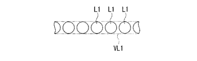
なお、中間層用の膜は、必ずしも連続したラインである必要はない。例えば、図4に示すように、導電膜配線を形成する仮想のラインVL1上に、液滴L1を離間した状態に配置し、中間層用の膜を、断続状態に形成してもよい。
また、中間層用の膜の厚みは、後述する導電膜配線用の膜の厚みに比べて薄くてよい。
【0040】
図2(b)に戻り、第2工程では、基板11上に配置された液体材料に含まれる分散媒の除去を行う。本例では、分散媒をすべて除去するのではなく、その一部だけを除去し、中間層用の膜を完全に乾燥させなくてもよい。乾燥しても微粒子は堆積しているだけで焼結しているわけではないため、その上に配置される導電膜配線用の液体材料の分散媒によって、堆積した微粒子はある程度再溶解する。従って、分散媒を一部除去しただけで、完全に除去した場合と同様の効果が期待できる。また、このような一部乾燥は、乾燥時間の短縮も目的としている。
分散媒の除去は、単に室温で放置するだけでもよく、加熱手段を用いて行ってもよい。例えば、ホットプレート、電気炉、熱風発生機などの加熱手段を用いた一般的な加熱処理の他に、ランプアニールを用いて行ってもよい。 なお、この際、液滴に含まれる分散媒がすべて除去され、乾燥膜に変換されるまで、加熱や光照射の度合いを高めても差し支えない。ただし、膜変換は、すべての液体材料の配置が終了してから、熱処理/光処理工程においてまとめて行えばよいので、ここでは、分散媒をある程度除去できれば十分であり、例えば、室温(25℃程度)で数分程度放置すればよい。しかし、中間層形成工程後に、加熱焼成や光処理にて中間層の膜変換を行なっても(例えば300℃程度の熱処理で)かまわない。
また、こうした処理は液体材料の吐出と並行して同時に進行させることも可能である。例えば、基板を予め加熱しておいたり、液体吐出ヘッドの冷却とともに沸点の低い分散媒を使用したりすることにより、基板に液滴を配置した直後から、その液滴の乾燥を進行させることができる。
【0041】
(材料配置工程)
次に、材料配置工程では、図1(b)に示すように、基板11上に形成された中間層用の膜W1の上に、液体吐出ヘッド10を介して、上記導電膜配線用の液体材料を液滴L2にして配置する。
ここで、図5(a)〜(c)は、基板上に上記液体材料を配置する過程をより具体的に示す図である。
【0042】
まず、図5(a)に示すように、液体吐出ヘッド10から吐出した液滴L2を、一定の間隔をあけて中間層の膜W1の上に順次配置する。本例では、液滴L2の配置ピッチP2は、基板11上に配置した直後の液滴L2の直径よりも大きくなるように定められている。また、液滴L2の配置ピッチP2は、基板11上に配置した直後の液滴L2の直径の2倍以下となるように定められている。
【0043】
次に、図5(b)に示すように、上述した液滴の配置動作を繰り返す。すなわち、図5(a)に示した前回と同様に、液体吐出ヘッド10から液体材料を液滴L3にして吐出し、その液滴L3を一定距離ごとに基板11に配置する。
このとき、液滴L3の体積(1つの液滴あたりの液体材料の量)、及びその配置ピッチP3は前回の液滴L2と同じである。また、液滴L3の配置位置を前回の液滴L2から1/2ピッチだけシフトさせ、基板11上に配置されている前回の液滴L2同士の中間位置に今回の液滴L3を配置する。
【0044】
上述したように、基板11上の液滴L2の配置ピッチP2は、基板11上に配置した直後の液滴L2の直径よりも大きくかつ、その直径の2倍以下である。そのため、液滴L2の中間位置に液滴L3が配置されることにより、液滴L2に液滴L3が一部重なり、液滴L2同士の間の隙間が埋まる。これにより、図5(c)に示すように、中間層の膜Wの上に、導電膜配線用の液体材料からなる連続したラインW2が形成される。そして、こうした液滴の配置動作を基板の表面全体に対して行うことにより、基板11上に所定のパターンからなる配線用の膜が形成される。
【0045】
このとき、前述したように、基板11の表面が撥液性に加工されていることから、液体材料は、中間層の膜W1の外側でははじかれ、中間層の膜W1上に確実に配置される。また、前述したように、中間層の膜W1は、導電膜配線用の液体材料の分散媒に対してある程度の再溶解があるため、上記液体材料との親和性が比較的高い。そのため、中間層の膜W1上に配置された液体材料は、中間層の膜W1の内側で良好に濡れ広がる。さらに、前述したように、中間層の膜W1は、導電膜配線の配線パターンと同一のパターンで形成されているので、中間層の膜W1の内側で濡れ広がった液体材料は、所望の配線パターンに良好に配置される。
【0046】
なお、基板11上に液滴を配置した後に、分散媒の一部除去を行うために、必要に応じて乾燥処理を行ってもよい。この乾燥処理は、例えば、一連の液滴の配置動作ごとに行われる。なお、この乾燥処理の目的と、その方法や装置は、中間層配置工程の第2工程と同じなので、ここでの説明は省略する。
【0047】
また、上述した液滴の配置動作の繰り返し回数を増やすことにより、基板11上に液滴が順次重なり、導電膜配線用の膜W2の厚みが増す。この膜厚は、最終的な導電膜配線に必要とされる所望の膜厚に応じて定められ、それに応じて、上記液滴の配置動作の繰り返し回数が定められる。
なお、液滴の配置ピッチや、繰り返しの際のシフト量などは任意に設定可能である。例えば、先の図2に示したように、吐出直後同士の液滴同士が一部重なるように液滴を吐出してもよい。
【0048】
(熱処理/光処理工程)
熱処理/光処理工程は、基板上に配置された液体材料に含まれる分散媒あるいはコーティング剤を完全に除去するとともに、金属微粒子同士の接触もしくは焼結をはかり、電気抵抗を下げるために行なわれる。なお、本例では、中間層用の液体材料の熱処理と導電膜配線用の液体材料の熱処理を同時に行なう。
【0049】
熱処理及び/又は光処理は通常大気中で行なわれるが、必要に応じて、窒素、アルゴン、ヘリウムなどの不活性ガス雰囲気中で行なうこともできる。熱処理及び/又は光処理の処理温度は、分散媒の沸点(蒸気圧)、雰囲気ガスの種類や圧力、微粒子の分散性や酸化性等の熱的挙動、コーティング材の有無や量、基材の耐熱温度などを考慮して適宜決定される。
たとえば、有機物からなるコーティング材を除去するためには、通常は200℃以上で焼成することが必要である。また、プラスチックなどの基板を使用する場合には、室温以上100℃以下で行なうことが好ましい。
【0050】
熱処理及び/又は光処理は通常のホットプレート、電気炉などによる処理の他、ランプアニールによって行なうこともできる。ランプアニールに使用する光の光源としては、特に限定されないが、赤外線ランプ、キセノンランプ、YAGレーザー、アルゴンレーザー、炭酸ガスレーザー、XeF、XeCl、XeBr、KrF、KrCl、ArF、ArClなどのエキシマレーザーなどを光源として使用することができる。これらの光源は一般には、出力10W以上5000W以下の範囲のものが用いられるが、本実施形態では100W以上1000W以下の範囲で十分である。
【0051】
上記熱処理及び/又は光処理により、導電膜配線用の膜W2は、液体材料に含まれていた導電性微粒子間の電気的接触が確保され、導電膜に変換される。
また、中間層用の膜W1は、液体材料に含まれていた微粒子の作用により、導電膜配線用の導電性微粒子と基板11との結合性を向上させる。
【0052】
本実施形態により形成される導電膜配線は、分散液一滴の基板上に着弾後の直径とほぼ同等の幅で形成することが可能である。また、中間層に含まれる金属微粒子によって、導電膜配線に含まれる金属微粒子と基板の両方に対する結合性が向上することから、基板に対する導電膜配線の密着力が高まる。
したがって、本実施形態によれば、導電膜配線の細線化とともに、基板に対する導電膜配線の密着力を高めることができる。
【0053】
(実施例1)
ここで、上記した導電膜配線の形成方法の実施形態に基づいて、ガラス基板上に導電膜配線を形成した実施例について説明する。
ガラス基板を洗浄し、さらに波長254nmの紫外線を10mW/cm2の強度で10分間照射して洗浄を行なった。これにより基板の表面は親液性となる。この基板と、ヘプタデカフルオロ−1,1,2,2,−テトラヒドロデシルトリエトキシシラン1gとを容量50リットルの密閉容器に入れて、120℃にて2時間放置した。これにより、基板表面全体にフルオロアルキル基を有する単分子膜が形成された。この表面と後述の金属微粒子が分散された液体材料との接触角は、中間層用、配線形成用の液体材料とも70°であった。さらに、この基板に上記と同じ紫外線を2分間照射して基板表面の液体材料との接触角を30°とした。
導電膜配線用の液体材料としては、粒径5nm程度の銀超微粒子が有機溶剤に分散した液体(真空冶金社製、商品名「パーフェクトシルバー」)の分散媒をテトラデカンに置換して、濃度が60重量%、粘度が8mPa・sとなるように調整した液を用いた。また、中間層用の液体材料としても、同様に粒径5nm程度のマンガンの超微粒子がテトラデカンに分散した液を用いた。このマンガン分散液の分散質濃度は4重量%であり、粘度は4mPa・sであった。これらの液体をセイコーエプソン製のインクジェットプリンターヘッド(市販プリンター商品名PM950Cと同等ヘッドを耐有機溶剤使用に改造したもの)を用いて基板上に所定パターンで吐出した。
まず、上記の接触角を30°とした基板表面に、マンガン分散液を所定のパターンで吐出した。液滴の大きさは約5ピコリットルであり、その直径は20μmであった。この液滴は基板に着弾後は40μm程度に広がった。このような液滴を38μmごとに(隣接した基板上の液滴と2μm、すなわち液滴の直径の5%の重なりが生じるように)吐出し、ライン状のパターンを形成した。基板の表面は撥液処理されているため、液滴が滲むようなことはなく、正確なエッジ形状のラインが形成された。
さらに、その後、分散媒を一部除去するために、室温(25℃程度)で2分間放置乾燥した後、銀の分散液を同様にしてマンガンの分散液と同じパターンで吐出した。その際、液滴の大きさは5ピコリットルで、マンガンのパターン上に40μmごとに吐出を行なった結果、マンガンのパターンと同じ形にぬれ広がり、外には出なかった。その後100℃の熱風を15秒間基板全体に吹き付けた後、再び銀の分散液を同様に40μmピッチで吐出した。さらに同様の熱風乾燥と40μmピッチの吐出を数回繰り返した。
最後に、基板全体を大気中で300℃にて30分間焼成し、膜厚3μm、線幅40μm、抵抗率2μΩcmの導電膜パターンが形成された。この導電膜パターンについての密着力試験としてテープ剥離試験を行なったところ、全く剥がれずに良好な密着力を示した。比較例として、上記ど同様の工程で中間層のない配線パターンを形成して同様に密着力を測定したところ、中間層があるほうが密着力が高かった。
(実施例2)
実施例1と同様の工程で、実施例1のマンガンの微粒子をそれぞれ、クロム、ニッケル、チタン、マグネシウム、シリコン、バナジウムの微粒子に変更して導電膜配線を形成したところ、いずれも実施例1と同様に密着力改善の効果が得られた。
【0054】
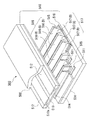
次に、本発明の電気光学装置の一例として、プラズマ型表示装置について説明する。
図6は本実施形態のプラズマ型表示装置500の分解斜視図を示している。
プラズマ型表示装置500は、互いに対向して配置されたガラス基板501、502、及びこれらの間に形成される放電表示部510を含んで構成される。
【0055】
ガラス基板501の上面には所定の間隔でストライプ状にアドレス電極511が形成され、アドレス電極511とガラス基板501の上面とを覆うように誘電体層519が形成されている。誘電体層519上には、アドレス電極511、511間に位置しかつ各アドレス電極511に沿うように隔壁515が形成されている。 また、隔壁515によって区画されるストライプ状の領域の内側には蛍光体517が配置されている。蛍光体517は、赤、緑、青の何れかの蛍光を発光するもので、赤色放電室516(R)の底部および側面には赤色蛍光体517(R)が、緑色放電室516(G)の底部および側面には緑色蛍光体517(G)が、青色放電室516(B)の底部および側面には青色蛍光体517(B)が各々配置されている。
【0056】
一方、ガラス基板502側には、先のアドレス電極511と直交する方向に複数の透明導電膜からなる表示電極512がストライプ状に所定の間隔で形成されるとともに、抵抗の高い表示電極512を補うために表示電極512上にバス電極512aが形成されている。またこれらを覆って誘電体層513が形成され、更にMgOなどからなる保護膜514が形成されている。
ガラス基板501とガラス基板502とは、前記アドレス電極511…と表示電極512…を互いに直交させるように対向させて相互に貼り合わされている。放電表示部510は、複数の放電室516が集合されたものである。複数の放電室516のうち、赤色放電室516(R)、緑色放電室516(G)、青色放電室516(B)の3つの放電室516が対になった部分と、一対の表示電極に囲まれた領域が1画素を構成するように配置されている。
上記アドレス電極511と表示電極512は図示略の交流電源に接続されている。各電極に通電することにより、放電表示部510において蛍光体517が励起発光し、カラー表示が可能となる。
【0057】
本実施形態では、上記バス電極512a、およびアドレス電極511が先の図1に示した導電膜配線の形成方法を用いて形成されている。そのため、バス電極512aとアドレス電極511の密着性が高く、配線不良が生じにくい。
なお、中間層がマンガン化合物(マンガンの酸化物)からなる場合、マンガンの酸化物は非導電性であるものの、そのマンガン層を非常に薄くかつポーラス状にすることで、表示電極512とバス電極512aとの必要な導電性は確保される。また、この場合、中間層が黒くなることから、この中間層がブラックマトリクス的な効果を奏し、表示コントラストの向上を図ることができる。
【0058】
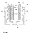
次に、本発明の電気光学装置の他の例として、液晶装置について説明する。
図7は、本実施形態に係る液晶装置の第1基板上の信号電極等の平面レイアウトを示すものである。本実施形態に係る液晶装置は、この第1基板と、走査電極等が設けられた第2基板(図示せず)と、第1基板と第2基板との間に封入された液晶(図示せず)とから概略構成されている。
【0059】
図7に示すように、第1基板300上の画素領域303には、複数の信号電極310…が多重マトリクス状に設けられている。特に各信号電極310…は、各画素に対応して設けられた複数の画素電極部分310a…とこれらを多重マトリクス状に接続する信号配線部分310b…とから構成されており、Y方向に伸延している。
また、符号350は1チップ構造の液晶駆動回路で、この液晶駆動回路350と信号配線部分310b…の一端側(図中下側)とが第1引き回し配線331…を介して接続されている。
また、符号340…は上下導通端子で、この上下導通端子340…と、図示しない第2基板上に設けられた端子とが上下導通材341…によって接続されている。また、上下導通端子340…と液晶駆動回路350とが第2引き回し配線332…を介して接続されている。
【0060】
本実施形態例では、上記第1基板300上に設けられた信号配線部分310b…、第1引き回し配線331…、及び第2引き回し配線332…がそれぞれ、先の図1に示した導電膜配線の形成方法に基づいて形成されている。そのため、配線の密着性が高く、配線不良が生じにくい。また、大型化した液晶用基板の製造に適用した場合においても、配線用材料を効率的に使用することができ、低コスト化が図れる。なお、本発明が適用できるデバイスは、これらの電気光学装置に限られず、例えば導電膜配線が形成される回路基板や、半導体の実装配線等、他のデバイス製造にも適用が可能である。
【0061】
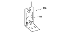
次に、本発明の電子機器の具体例について説明する。
図8は、携帯電話の一例を示した斜視図である。図9において、600は携帯電話本体を示し、601は先の図7に示した液晶装置を備えた液晶表示部を示している。
図9は、ワープロ、パソコンなどの携帯型情報処理装置の一例を示した斜視図である。図9において、700は情報処理装置、701はキーボードなどの入力部、703は情報処理本体、702は先の図7に示した液晶装置を備えた液晶表示部を示している。
図10は、腕時計型電子機器の一例を示した斜視図である。図10において、800は時計本体を示し、801は先の図7に示した液晶装置を備えた液晶表示部を示している。
図8〜図10に示す電子機器は、上記実施形態の液晶装置を備えたものであるので、配線の密着性が高く、配線不良が生じにくい。
なお、本実施形態の電子機器は液晶装置を備えるものとしたが、有機エレクトロルミネッセンス表示装置、プラズマ型表示装置等、他の電気光学装置を備えた電子機器とすることもできる。
【0062】
以上、添付図面を参照しながら本発明に係る好適な実施形態について説明したが、本発明は係る例に限定されないことは言うまでもない。上述した例において示した各構成部材の諸形状や組み合わせ等は一例であって、本発明の主旨から逸脱しない範囲において設計要求等に基づき種々変更可能である。
【0063】
【発明の効果】
本発明の導電膜配線の形成方法によれば、基板の表面を撥液性に制御する表面処理工程と、中間層を形成する中間層形成工程とを有することにより、導電膜配線の細線化とともに、基板に対する導電膜配線の密着力を高めることができる。
【0064】
本発明の膜構造体によれば、導電膜配線の細線化及び密着性の向上を図ることができる。
【0065】
本発明の電気光学装置によれば、配線不良が生じにくく、品質の向上を図ることができる。
【図面の簡単な説明】
【図1】 本実施形態に係る配線形成方法を模式的に示す図である。
【図2】 基板上に中間層を形成する手順の一例を模式的に示す図である。
【図3】 基板上に形成される中間層用の膜の一例として、直線状のラインを示す平面図である。
【図4】 基板上に形成される中間層用の膜の一例として、断続状態のラインを示す平面図である。
【図5】 基板上に液体材料を配置する過程をより具体的に示す図である。
【図6】 本発明の電気光学装置を、プラズマ型表示装置に適用した例を示す分解斜視図である。
【図7】 本発明の電気光学装置を、液晶装置に適用した例を示す平面図である。
【図8】 本発明の電子機器を、液晶表示装置を備えた携帯電話に適用した例を示す図である。
【図9】 本発明の電子機器を、液晶表示装置を備えた携帯型上方処理装置に適用した例を示す図である。
【図10】 本発明の電子機器を、液晶表示装置を備えた腕時計型電子機器に適用した例を示す図である。
【符号の説明】
10…液体吐出ヘッド(液体吐出手段)、11…基板、W1…中間層、W2…導電膜配線、L1、L2、L3…液滴、P1、P2、P3…ピッチ。[0001]
BACKGROUND OF THE INVENTION
The present invention provides a substrate onConductive film wiringIn particular, a liquid material containing metal fine particles is disposed on a substrate via a liquid discharge means, and a predetermined pattern is formed on the substrate.Conductive film wiringIt relates to a method of forming.
[0002]
[Prior art]
As a technique for forming the conductive film wiring on the substrate, a material film for the conductive film wiring is formed on the substrate using a coating technique such as a spin coating method, and this film is formed into a desired pattern using a photolithography method. Methods of forming are known.
[0003]
[Problems to be solved by the invention]
On the other hand, in recent years, a technique has been proposed in which a liquid material is disposed at a desired position on a substrate and a pattern of conductive film wiring is directly formed on the substrate. In this technique, the steps related to photolithography can be omitted or simplified.
[0004]
As a technique for arranging the liquid material at a desired position on the substrate, there is a technique for ejecting the liquid material as droplets via a nozzle provided in the liquid ejection means. This technique has advantages in that the consumption of the liquid material is less wasteful than the coating technique such as the spin coating method, and the amount and position of the liquid material arranged on the substrate can be easily controlled.
[0005]
However, it is difficult to thin the conductive film wiring by the technique of disposing the liquid material on the substrate through the liquid discharging means. By controlling the surface of the substrate to be liquid repellent, it is possible to reduce the thickness of the conductive film wiring. However, in this case, the adhesion of the conductive film wiring to the substrate tends to decrease.
[0006]
The present invention has been made in view of the above circumstances,Conductive film wiringAs the wire becomes thinner,Conductive film wiringCan improve the adhesion ofConductive film wiringIt aims at providing the formation method of this.
In addition, another object of the present invention is to achieve thinning and improved adhesion.Conductive film wiringIt is providing a membrane structure provided with.
Another object of the present invention is to provide an electro-optical device and an electronic apparatus that are unlikely to cause wiring defects.
[0007]
[Means for Solving the Problems]
The method for forming a conductive film wiring of the present invention is a method of disposing a first liquid material containing first metal particles on a substrate via a liquid discharge means, and forming the conductive film wiring on the substrate. Before placing the first liquid material on the substrate, the surface of the substrate is made liquid repellent with respect to the first liquid material and a second liquid material different from the first liquid material. A surface treatment step to be controlled; and after the surface treatment step, the second liquid material is applied to the substrate via a liquid discharge means.Surface controlled by liquid repellencyAnd an intermediate layer forming step for forming an intermediate layer for improving the adhesion of the conductive film wiring to the substrate, wherein the second liquid material is a second different from the first metal particles. The second particles are particles containing at least one metal selected from the group consisting of manganese, chromium, nickel, titanium, magnesium, silicon, and vanadium or an oxide of the metal. And Here, “liquid repellency” refers to a characteristic that exhibits non-affinity for a liquid material.
[0008]
In the above method for forming a conductive film wiring, the first liquid material for the conductive film wiring is arranged on the substrate through the liquid discharge means, so that the process is simplified compared to the technique using the photolithography method. And material consumption can be reduced. In addition, by controlling the surface of the substrate to be liquid repellent, the spread of the first liquid material disposed on the substrate is suppressed, and the conductive film wiring can be thinned. Further, in the above method for forming the conductive film wiring, the intermediate layer made of the second liquid material is formed on the substrate controlled to be liquid repellent so that the substance contained in the second liquid material is the first. Since the bonding property to both the metal fine particles and the substrate is improved, the adhesion of the conductive film wiring to the substrate can be increased.
[0009]
In the above method for forming a conductive film wiring, the intermediate layer may be formed on a part of the substrate corresponding to the shape of the conductive film wiring.
Preferably, the intermediate layer is formed in the same pattern as the conductive film wiring, and the first liquid material is disposed on the pattern of the intermediate layer.
In this case, since the first liquid material is repelled on the surface of the substrate controlled to be liquid repellent outside the intermediate layer pattern, the first liquid material is reliably disposed on the intermediate layer pattern. Thereby, the first liquid material is satisfactorily arranged in the predetermined pattern.
The intermediate layer may employ a technique in which a plurality of films are arranged in a state of being separated from each other.
[0010]
In the conductive film wiring forming method, at least a part of the dispersion medium of the second liquid material disposed on the substrate is removed before the first liquid material is disposed on the substrate. It is preferable to do this.
By removing at least part of the dispersion medium of the second liquid material, the first liquid material can be satisfactorily disposed on the second liquid material layer. Note that it is only necessary to remove a part of the dispersion medium of the second liquid material, and it is not always necessary to remove all of the dispersion medium. Alternatively, the fine metal particles contained in the second liquid material may be sintered or oxidized after the dispersion medium is removed.
[0011]
The conductive film wiring forming method may further include a step of collectively converting the first liquid material and the second liquid material disposed on the substrate into a film by heat treatment or light treatment. .
Through throughput of the first liquid material and the second liquid material can be improved by heat treatment or light treatment.
[0012]
In the method for forming a conductive film wiring, second fine particles different from the first metal fine particles are used as the second liquid material. As such second fine particles, for example, fine particles containing manganese, chromium, nickel, titanium, magnesium, silicon, vanadium, alloys thereof, or oxides thereof are used. Furthermore, the organometallic compound of the said metal is contained.
When the above-mentioned fine particles are contained in the second liquid material, when the intermediate layer is formed using the liquid material, oxides thereof are easily formed. Since these oxides are often black, for example, a black intermediate layer is disposed at a visible position such as a bus electrode disposed in the vicinity of the display electrode, thereby providing a black matrix effect. It is possible to improve the display contrast.
[0013]
Further, for example, a transparent electrode film is formed on the surface of the substrate, and as the first liquid material, for example, a material containing silver fine particles is used.
When a silver film is formed on a transparent electrode film, both may react to cause a color change, but by providing an intermediate layer containing manganese or the like between the two, the above color change can be prevented. .
[0014]
The film structure of the present invention is a film structure including a substrate and a conductive film wiring having a predetermined pattern formed on the substrate, and the conductive film wiring is formed by the conductive film wiring forming method described above. It is formed.
In this film structure, since the conductive film wiring can be formed by a simple process, the cost can be reduced. Further, the conductive film wiring can be made thinner and the adhesion can be improved.
[0015]
The method for producing a film structure of the present invention is characterized by using the above-described method for forming a conductive film of the present invention.
A method for manufacturing an electro-optical device according to the present invention is characterized by using the above-described method for forming a film structure according to the present invention.
An electronic apparatus manufacturing method according to the present invention is characterized by using the above-described method for forming an electro-optical device according to the present invention.
Examples of the electro-optical device include a liquid crystal display device, an organic electroluminescence display device, and a plasma display device.
According to the method for manufacturing a film structure of the present invention, since the conductive film can be formed by a simple process, the cost can be reduced. In addition, thinning of the conductive film and improvement in adhesion can be achieved.
According to the electro-optical device manufacturing method and the electronic device manufacturing method of the present invention, since the conductive film wiring has high adhesion, it is possible to manufacture an electro-optical device or electronic device in which wiring defects are unlikely to occur.
[0016]
DETAILED DESCRIPTION OF THE INVENTION
Next, as an example of an embodiment according to the present invention, a method for forming a conductive film wiring on a substrate will be described.
FIGS. 1A to 1C are diagrams schematically illustrating a wiring forming method according to the present embodiment. In this wiring forming method, a liquid material is placed on a substrate, and a conductive film pattern for wiring is formed on the substrate. The surface treatment step, the intermediate layer forming step (FIG. 1A), the material placement A process (FIG. 1B), a heat treatment / light treatment process (FIG. 1C), and the like.
Here, the intermediate layer forming step is a step of forming an intermediate layer disposed between the substrate and the conductive film wiring, and this intermediate layer has a role of improving the adhesion of the conductive film wiring to the substrate.
In the intermediate layer forming step and the material arranging step, predetermined liquid materials are arranged on the substrate. That is, in the material arranging step, a liquid material (first liquid material) containing first metal fine particles for forming the conductive film wiring is used, and in the intermediate layer forming step, a liquid material (second liquid) different from the first is used. Liquid material). For the arrangement of these liquid materials, a liquid discharge method in which the liquid material is discharged as droplets via a nozzle of a liquid discharge head, a so-called inkjet method is used.
First, the liquid material used in the material arranging step and the intermediate layer forming step will be described.
[0017]
In this example, a liquid dispersion in which metal fine particles are dispersed in a dispersion medium is used as the liquid material used in the material arranging step. The conductive fine particles used here are metal fine particles containing any of silver, gold, copper, palladium, and nickel.
These metal fine particles can be used by coating the surface with an organic substance or the like in order to improve dispersibility.
The particle diameter of the conductive fine particles is preferably 1 nm or more and 0.1 μm or less. If it is larger than 0.1 μm, the nozzle of the liquid discharge head may be clogged. On the other hand, when the particle size is smaller than 1 nm, the dispersibility of the metal fine particles is deteriorated, the volume ratio of the coating agent to the metal fine particles is increased, and the ratio of the organic matter in the obtained film is excessive.
[0018]
As the liquid dispersion medium containing metal fine particles, those having a vapor pressure at room temperature of 0.001 mmHg to 200 mmHg (about 0.133 Pa to 26600 Pa) are preferable. When the vapor pressure is higher than 200 mmHg, the dispersion medium rapidly evaporates after ejection, making it difficult to form a good film.
The vapor pressure of the dispersion medium is more preferably 0.001 mmHg to 50 mmHg (about 0.133 Pa to 6650 Pa). When the vapor pressure is higher than 50 mmHg, nozzle clogging due to drying tends to occur when droplets are ejected by the ink jet method, and stable ejection becomes difficult.
On the other hand, in the case of a dispersion medium having a vapor pressure lower than 0.001 mmHg at room temperature, drying is slow and the dispersion medium tends to remain in the film, and a high-quality conductive film can be obtained after heat and / or light treatment in the subsequent process. Hateful.
[0019]
The dispersion medium is not particularly limited as long as it can disperse the conductive fine particles and does not cause aggregation. In addition to water, alcohols such as methanol, ethanol, propanol, and butanol, n-heptane , N-octane, decane, toluene, xylene, cyclone, durene, indene, dipentene, tetrahydronaphthalene, decahydronaphthalene, cyclohexylbenzene and other hydrocarbon compounds, ethylene glycol dimethyl ether, ethylene glycol diethyl ether, ethylene glycol methyl ethyl ether , Diethylene glycol dimethyl ether, diethylene glycol diethyl ether, diethylene glycol methyl ethyl ether, 1,2-dimethoxyethane, bis (2-methoxyethyl) ether Ether compounds such as p- dioxane, propylene carbonate, .gamma.-butyrolactone, N- methyl-2-pyrrolidone, dimethylformamide, dimethyl sulfoxide, may be mentioned polar compounds such as cyclohexanone. Of these, water, alcohols, hydrocarbon compounds, and ether compounds are preferred from the viewpoints of fine particle dispersibility, dispersion stability, and ease of application to the inkjet method, and more preferred dispersion media. Can include water and hydrocarbon compounds. These dispersion media can be used alone or as a mixture of two or more.
[0020]
The dispersoid concentration in the case where the conductive fine particles are dispersed in the dispersion medium is 1% by mass or more and 80% by mass or less, and can be adjusted according to the desired film thickness of the conductive film. If it exceeds 80% by mass, aggregation tends to occur and it is difficult to obtain a uniform film.
[0021]
The surface tension of the conductive fine particle dispersion is preferably in the range of 0.02 N / m to 0.07 N / m. When the liquid is ejected by the ink jet method, if the surface tension is less than 0.02 N / m, the wettability of the ink composition to the nozzle surface increases, and thus flight bending tends to occur, exceeding 0.07 N / m. Since the shape of the meniscus at the nozzle tip is not stable, it becomes difficult to control the discharge amount and the discharge timing.
[0022]
In order to adjust the surface tension, a small amount of a surface tension adjusting agent such as a fluorine-based, silicone-based, or nonionic-based material may be added to the dispersion within a range that does not unduly reduce the contact angle with the substrate. The nonionic surface tension modifier improves the wettability of the liquid to the substrate, improves the leveling property of the film, and helps prevent the occurrence of fine irregularities in the film.
The dispersion liquid may contain an organic compound such as alcohol, ether, ester, or ketone, if necessary.
[0023]
The viscosity of the dispersion is preferably 1 mPa · s to 50 mPa · s. When discharging by the inkjet method, if the viscosity is less than 1 mPa · s, the nozzle periphery is easily contaminated by the outflow of ink, and if the viscosity is more than 50 mPa · s, the nozzle hole is clogged frequently. Therefore, it becomes difficult to smoothly discharge droplets.
[0024]
On the other hand, as the liquid material used in the intermediate layer forming step, a dispersion liquid in which metal fine particles are dispersed in a dispersion medium is used in this example. As the metal fine particles used here, those that have been confirmed to have an effect of improving the bonding property between the first metal fine particles and the substrate described above through a heat treatment / light treatment process described later are used. The fine particles may be conductive or non-conductive. For example, as the fine particles, manganese, copper, and metal fine particles containing any of chromium, nickel, titanium, magnesium, silicon, vanadium, alloys thereof, or oxides thereof are used. The liquid material may contain an organometallic compound of the above metal.
[0025]
The particle diameter of the metal fine particles used in the intermediate layer forming step is preferably 1 nm or more and 0.1 μm or less. If it is larger than 0.1 μm, the nozzle of the liquid discharge head may be clogged.
[0026]
As the liquid dispersion medium containing the metal fine particles used in the intermediate layer forming step, the same dispersion medium as the metal fine particle used in the material arranging step can be used, and the description thereof is omitted here. The same applies to the dispersoid concentration when the fine particles are dispersed in the dispersion medium. The same applies to the surface tension and additives of the fine particle dispersion, and a description thereof will be omitted.
[0027]
Next, the above steps will be described in detail.
(Surface treatment process)
In the surface treatment process, the surface of the substrate on which the conductive film wiring is formed is processed to be liquid repellent with respect to the liquid material used in the material arranging process and the liquid material used in the intermediate layer forming process. Specifically, the surface treatment is performed so that a predetermined contact angle with respect to the liquid material is 30 [deg] or more and 60 [deg] or less.
Various substrates such as Si wafer, quartz glass, glass, plastic film, and metal plate can be used as the conductive film wiring substrate. Further, a substrate in which a semiconductor film, a metal film, a dielectric film, an organic film or the like is formed as a base layer on the surface of these various material substrates may be used as a substrate on which conductive film wiring is to be formed.
As a method for controlling the liquid repellency (wetting property) of the surface, for example, a method of forming a self-assembled film on the surface of the substrate, a plasma treatment method, or the like can be employed.
[0028]
In the self-assembled film forming method, a self-assembled film made of an organic molecular film or the like is formed on the surface of a substrate on which conductive film wiring is to be formed.
The organic molecular film for treating the substrate surface has a functional group that can bind to the substrate and a functional group that modifies the surface properties of the substrate, such as a lyophilic group or a liquid repellent group, on the opposite side (controls the surface energy). And a carbon straight chain or a partially branched carbon chain connecting these functional groups, and is bonded to a substrate and self-assembles to form a molecular film, for example, a monomolecular film.
[0029]
Here, the self-assembled film is composed of a binding functional group capable of reacting with constituent atoms such as a base layer such as a substrate and other linear molecules, and has extremely high orientation due to the interaction of the linear molecules. It is a film formed by orienting a compound. Since this self-assembled film is formed by orienting single molecules, the film thickness can be extremely reduced, and the film is uniform at the molecular level. That is, since the same molecule is located on the surface of the film, uniform and excellent liquid repellency and lyophilicity can be imparted to the surface of the film.
[0030]
By using, for example, fluoroalkylsilane as the compound having high orientation, each compound is oriented so that the fluoroalkyl group is located on the surface of the film, and a self-assembled film is formed. Liquid repellency is imparted.
[0031]
Examples of compounds that form a self-assembled film include heptadecafluoro-1,1,2,2 tetrahydrodecyltriethoxysilane, heptadecafluoro-1,1,2,2 tetrahydrodecyltrimethoxysilane, heptadecafluoro-1 , 1,2,2 tetrahydrodecyltrichlorosilane, tridecafluoro-1,1,2,2 tetrahydrooctyltriethoxysilane, tridecafluoro-1,1,2,2 tetrahydrooctyltrimethoxysilane, tridecafluoro-1 , 1,2,2 tetrahydrooctyltrichlorosilane, trifluoropropyltrimethoxysilane, and other fluoroalkylsilanes (hereinafter referred to as “FAS”). In use, one compound may be used alone, or two or more compounds may be used in combination. Note that by using FAS, adhesion to the substrate and good liquid repellency can be obtained.
[0032]
FAS generally has the structural formula RnSiX(4-n)It is represented by Here, n represents an integer of 1 to 3, and X is a hydrolyzable group such as a methoxy group, an ethoxy group, or a halogen atom. R is a fluoroalkyl group, and (CFThree) (CF2) X (CH2) Y (where x represents an integer from 0 to 10 and y represents an integer from 0 to 4), and when a plurality of R or X are bonded to Si, R or Each X may be the same or different. The hydrolyzable group represented by X forms silanol by hydrolysis, reacts with the hydroxyl group of the base such as the substrate (glass, silicon), etc., and bonds to the substrate with a siloxane bond. On the other hand, since R has a fluoro group such as (CF3) on the surface, the base surface such as a substrate is modified to a surface that does not get wet (surface energy is low).
[0033]
A self-assembled film made of an organic molecular film or the like is formed on a substrate when the above raw material compound and the substrate are placed in the same sealed container and left at room temperature for about 2 to 3 days. Further, by holding the entire sealed container at 100 ° C., it is formed on the substrate in about 3 hours. What has been described above is the formation method from the gas phase, but the self-assembled film can also be formed from the liquid phase. For example, the self-assembled film can be obtained on the substrate by immersing the substrate in a solution containing the raw material compound, washing and drying.
Note that before the self-assembled film is formed, it is desirable to perform pretreatment by irradiating the substrate surface with ultraviolet light or washing with a solvent.
[0034]
In the plasma processing method, the substrate is irradiated with plasma under normal pressure or vacuum. Various types of gas used for the plasma treatment can be selected in consideration of the surface material of the substrate on which the conductive film wiring is to be formed. Examples of the processing gas include tetrafluoromethane, perfluorohexane, perfluorodecane, and the like.
[0035]
In addition, the process which processes the surface of a board | substrate to liquid repellency can also be performed by sticking to the board | substrate surface the film which has desired liquid repellency, for example, the polyimide film etc. which were tetrafluoroethylene processed. Moreover, you may use said polyimide film as a board | substrate as it is.
In addition, when the substrate surface has a liquid repellency higher than the desired liquid repellency, a treatment to make the substrate surface lyophilic by irradiating with ultraviolet light of 170 to 400 nm or exposing the substrate to an ozone atmosphere. Go and control the surface condition.
[0036]
(Intermediate layer forming process)
2A and 2B are diagrams schematically showing an example of a procedure for forming an intermediate layer on a substrate. As described above, this intermediate layer is for improving the adhesion of the conductive film wiring to the substrate.
The intermediate layer forming step includes a first step (FIG. 2 (a)) for disposing a liquid material on a substrate processed to be liquid repellent, and a medium (dispersion medium) contained in the liquid material disposed on the substrate. And a second step (FIG. 2B) for removing at least a part.
[0037]
In the first step, as shown in FIG. 2A, the liquid material for forming the intermediate layer is dropped through the
Then, such a droplet placement operation is performed on the entire surface of the substrate to form a film having a predetermined pattern on the
Note that, as in the material arranging step described later, the arrangement pitch of the droplets may be larger than the diameter of the droplets immediately after being arranged on the substrate. In this case, a continuous line is formed by repeatedly placing the liquid droplets a plurality of times on the same portion while shifting the start position after the drying process is sandwiched in the middle.
[0038]
The droplet discharge conditions, in particular, the volume of the droplets and the arrangement pitch of the droplets are determined so that the shape of the edge of the line formed on the
[0039]
FIG. 3 is a plan view showing a straight line as an example of the intermediate layer film formed on the substrate. As described above, such a continuous line W <b> 1 can be formed on the
Note that the film for the intermediate layer is not necessarily a continuous line. For example, as shown in FIG. 4, the droplet L1 may be arranged on the virtual line VL1 forming the conductive film wiring so as to be separated, and the intermediate layer film may be formed in an intermittent state.
The thickness of the intermediate layer film may be smaller than the thickness of the conductive film wiring film described later.
[0040]
Returning to FIG. 2B, in the second step, the dispersion medium contained in the liquid material disposed on the
The removal of the dispersion medium may be simply left at room temperature or may be performed using a heating means. For example, lamp annealing may be used in addition to general heat treatment using a heating means such as a hot plate, an electric furnace, or a hot air generator. At this time, the degree of heating or light irradiation may be increased until all of the dispersion medium contained in the droplets is removed and converted into a dry film. However, since the film conversion may be performed collectively in the heat treatment / light treatment process after the arrangement of all the liquid materials is completed, it is sufficient here that the dispersion medium can be removed to some extent, for example, at room temperature (25 ° C. Just leave it for a few minutes. However, after the intermediate layer formation step, film conversion of the intermediate layer may be performed by heating and baking or light treatment (for example, by heat treatment at about 300 ° C.).
Also, such processing can proceed simultaneously with the discharge of the liquid material. For example, by previously heating the substrate or using a dispersion medium having a low boiling point along with cooling of the liquid discharge head, drying of the droplet can proceed immediately after the droplet is placed on the substrate. it can.
[0041]
(Material placement process)
Next, in the material arranging step, as shown in FIG. 1B, the liquid for the conductive film wiring is formed on the intermediate layer film W <b> 1 formed on the
Here, FIGS. 5A to 5C are diagrams more specifically showing the process of arranging the liquid material on the substrate.
[0042]
First, as shown in FIG. 5A, the droplets L2 ejected from the
[0043]
Next, as shown in FIG. 5B, the above-described droplet placement operation is repeated. That is, as in the previous time shown in FIG. 5A, the liquid material is ejected from the
At this time, the volume of the droplet L3 (the amount of the liquid material per droplet) and the arrangement pitch P3 thereof are the same as those of the previous droplet L2. Further, the arrangement position of the droplet L3 is shifted by 1/2 pitch from the previous droplet L2, and the current droplet L3 is arranged at an intermediate position between the previous droplets L2 arranged on the
[0044]
As described above, the arrangement pitch P2 of the droplets L2 on the
[0045]
At this time, as described above, since the surface of the
[0046]
In addition, after arrange | positioning a droplet on the board |
[0047]
In addition, by increasing the number of repetitions of the above-described droplet placement operation, the droplets sequentially overlap the
The arrangement pitch of the droplets, the shift amount at the time of repetition, and the like can be arbitrarily set. For example, as shown in FIG. 2, the droplets may be ejected so that the droplets immediately after ejection partially overlap each other.
[0048]
(Heat treatment / light treatment process)
The heat treatment / light treatment step is performed to completely remove the dispersion medium or coating agent contained in the liquid material arranged on the substrate, and to contact or sinter metal fine particles to lower the electrical resistance. In this example, the heat treatment of the liquid material for the intermediate layer and the heat treatment of the liquid material for the conductive film wiring are performed simultaneously.
[0049]
The heat treatment and / or light treatment is usually performed in the air, but may be performed in an inert gas atmosphere such as nitrogen, argon, helium, etc., if necessary. The treatment temperature of heat treatment and / or light treatment depends on the boiling point (vapor pressure) of the dispersion medium, the type and pressure of the atmospheric gas, the thermal behavior such as fine particle dispersibility and oxidation, the presence and amount of coating material, It is determined appropriately in consideration of the heat resistant temperature.
For example, in order to remove a coating material made of an organic material, it is usually necessary to bake at 200 ° C. or higher. Moreover, when using a board | substrate, such as a plastic, it is preferable to carry out at room temperature or more and 100 degrees C or less.
[0050]
The heat treatment and / or light treatment can be performed by lamp annealing in addition to the treatment by a normal hot plate, electric furnace or the like. The light source used for lamp annealing is not particularly limited, but excimer laser such as infrared lamp, xenon lamp, YAG laser, argon laser, carbon dioxide laser, XeF, XeCl, XeBr, KrF, KrCl, ArF, ArCl, etc. Can be used as a light source. In general, these light sources have an output in the range of 10 W to 5000 W, but in the present embodiment, a range of 100 W to 1000 W is sufficient.
[0051]
By the heat treatment and / or light treatment, the conductive film wiring film W2 is converted into a conductive film while ensuring electrical contact between the conductive fine particles contained in the liquid material.
The intermediate layer film W1 improves the bonding between the conductive fine particles for conductive film wiring and the
[0052]
The conductive film wiring formed according to the present embodiment can be formed on the substrate of one droplet of the dispersion liquid with a width substantially equal to the diameter after landing. In addition, since the metal fine particles contained in the intermediate layer improve the bonding property to both the metal fine particles contained in the conductive film wiring and the substrate, the adhesion of the conductive film wiring to the substrate is enhanced.
Therefore, according to the present embodiment, the adhesion of the conductive film wiring to the substrate can be increased along with the thinning of the conductive film wiring.
[0053]
(Example 1)
Here, the Example which formed the electrically conductive film wiring on the glass substrate based on embodiment of the formation method of the above electrically conductive film wiring is demonstrated.
The glass substrate was washed, and further washed by irradiating ultraviolet rays having a wavelength of 254 nm with an intensity of 10 mW / cm 2 for 10 minutes. This makes the surface of the substrate lyophilic. This substrate and 1 g of heptadecafluoro-1,1,2,2, -tetrahydrodecyltriethoxysilane were put in a sealed container having a capacity of 50 liters and left at 120 ° C. for 2 hours. As a result, a monomolecular film having a fluoroalkyl group was formed on the entire substrate surface. The contact angle between this surface and the liquid material in which metal fine particles described later were dispersed was 70 ° for both the intermediate layer and the wiring formation liquid material. Further, this substrate was irradiated with the same ultraviolet rays as described above for 2 minutes, so that the contact angle with the liquid material on the substrate surface was 30 °.
As a liquid material for conductive film wiring, a dispersion medium of a liquid (trade name “Perfect Silver” manufactured by Vacuum Metallurgical Co., Ltd.) in which silver ultrafine particles having a particle diameter of about 5 nm are dispersed in an organic solvent is replaced with tetradecane, and the concentration A liquid adjusted to 60% by weight and a viscosity of 8 mPa · s was used. Similarly, a liquid in which ultrafine manganese particles having a particle diameter of about 5 nm are dispersed in tetradecane was used as the liquid material for the intermediate layer. The manganese dispersion had a dispersoid concentration of 4% by weight and a viscosity of 4 mPa · s. These liquids were ejected in a predetermined pattern onto a substrate using an ink-jet printer head manufactured by Seiko Epson (a head equivalent to a commercial printer product name PM950C modified to use an organic solvent).
First, a manganese dispersion was discharged in a predetermined pattern onto the substrate surface with the contact angle of 30 °. The droplet size was about 5 picoliters and its diameter was 20 μm. The droplet spread to about 40 μm after landing on the substrate. Such droplets were discharged every 38 μm (so that the droplets on the adjacent substrate were 2 μm, that is, 5% of the diameter of the droplets overlapped) to form a line pattern. Since the surface of the substrate was subjected to a liquid repellent treatment, the droplets did not bleed and an accurate edge-shaped line was formed.
Further, in order to remove a part of the dispersion medium, the film was left to dry at room temperature (about 25 ° C.) for 2 minutes, and then the silver dispersion liquid was discharged in the same pattern as the manganese dispersion liquid. At that time, the size of the droplet was 5 picoliters. As a result of discharging every 40 μm on the manganese pattern, the droplet spread out in the same shape as the manganese pattern and did not come out. Thereafter, hot air of 100 ° C. was blown over the entire substrate for 15 seconds, and then the silver dispersion was similarly discharged at a pitch of 40 μm. Further, similar hot air drying and 40 μm pitch discharge were repeated several times.
Finally, the entire substrate was baked at 300 ° C. for 30 minutes in the atmosphere to form a conductive film pattern having a film thickness of 3 μm, a line width of 40 μm, and a resistivity of 2 μΩcm. When a tape peeling test was conducted as an adhesion test for this conductive film pattern, it showed good adhesion without peeling off at all. As a comparative example, when a wiring pattern without an intermediate layer was formed in the same process as described above and the adhesion was measured in the same manner, the adhesion was higher when the intermediate layer was present.
(Example 2)
In the same process as Example 1, the manganese fine particles of Example 1 were changed to chromium, nickel, titanium, magnesium, silicon, and vanadium fine particles, respectively, and conductive film wiring was formed. Similarly, the effect of improving the adhesion was obtained.
[0054]
Next, a plasma display device will be described as an example of the electro-optical device of the present invention.
FIG. 6 is an exploded perspective view of the
The
[0055]
[0056]
On the other hand, on the
The
The
[0057]
In the present embodiment, the
When the intermediate layer is made of a manganese compound (manganese oxide), the manganese oxide is non-conductive, but the manganese layer is made very thin and porous so that the
[0058]
Next, a liquid crystal device will be described as another example of the electro-optical device of the invention.
FIG. 7 shows a planar layout of signal electrodes and the like on the first substrate of the liquid crystal device according to this embodiment. The liquid crystal device according to this embodiment includes the first substrate, a second substrate (not shown) provided with scanning electrodes and the like, and a liquid crystal (not shown) sealed between the first substrate and the second substrate. )).
[0059]
As shown in FIG. 7, a plurality of
Further,
[0060]
In the present embodiment example, the
[0061]
Next, specific examples of the electronic device of the present invention will be described.
FIG. 8 is a perspective view showing an example of a mobile phone. In FIG. 9,
FIG. 9 is a perspective view showing an example of a portable information processing apparatus such as a word processor or a personal computer. In FIG. 9,
FIG. 10 is a perspective view showing an example of a wristwatch type electronic apparatus. In FIG. 10,
Since the electronic apparatus shown in FIGS. 8 to 10 includes the liquid crystal device according to the above-described embodiment, the adhesion of wiring is high, and wiring defects are unlikely to occur.
In addition, although the electronic device of this embodiment shall be provided with a liquid crystal device, it can also be set as the electronic device provided with other electro-optical devices, such as an organic electroluminescent display apparatus and a plasma type display apparatus.
[0062]
As described above, the preferred embodiments according to the present invention have been described with reference to the accompanying drawings, but the present invention is not limited to the examples. Various shapes, combinations, and the like of the constituent members shown in the above-described examples are examples, and various modifications can be made based on design requirements and the like without departing from the gist of the present invention.
[0063]
【The invention's effect】
According to the method for forming a conductive film wiring of the present invention, by having a surface treatment step for controlling the surface of the substrate to be liquid repellent and an intermediate layer forming step for forming an intermediate layer, along with the thinning of the conductive film wiring The adhesion of the conductive film wiring to the substrate can be increased.
[0064]
According to the film structure of the present invention, it is possible to reduce the thickness of the conductive film wiring and improve the adhesion.
[0065]
According to the electro-optical device of the present invention, poor wiring hardly occurs and quality can be improved.
[Brief description of the drawings]
FIG. 1 is a diagram schematically showing a wiring forming method according to an embodiment.
FIG. 2 is a diagram schematically showing an example of a procedure for forming an intermediate layer on a substrate.
FIG. 3 is a plan view showing a straight line as an example of a film for an intermediate layer formed on a substrate.
FIG. 4 is a plan view showing an intermittent line as an example of a film for an intermediate layer formed on a substrate.
FIG. 5 is a diagram more specifically showing a process of disposing a liquid material on a substrate.
FIG. 6 is an exploded perspective view showing an example in which the electro-optical device of the invention is applied to a plasma display device.
FIG. 7 is a plan view showing an example in which the electro-optical device of the invention is applied to a liquid crystal device.
FIG. 8 is a diagram illustrating an example in which the electronic apparatus of the invention is applied to a mobile phone including a liquid crystal display device.
FIG. 9 is a diagram showing an example in which the electronic apparatus of the present invention is applied to a portable upper processing apparatus equipped with a liquid crystal display device.
FIG. 10 is a diagram showing an example in which the electronic apparatus of the present invention is applied to a wristwatch type electronic apparatus equipped with a liquid crystal display device.
[Explanation of symbols]
DESCRIPTION OF
Claims (10)
前記第1の液体材料を前記基板上に配置する前に、
前記基板の表面を前記第1の液体材料および前記第1の液体材料とは異なる第2の液体材料に対して撥液性に制御する表面処理工程と、
前記表面処理工程の後に、液体吐出手段を介して前記第2の液体材料を前記基板の撥液性に制御された表面上に配置し、前記基板に対する前記導電膜配線の密着力を向上させる中間層を形成する中間層形成工程とを有し、
前記第2の液体材料は、前記第1の金属粒子と異なる第2の粒子を含み、
前記第2の粒子は、マンガン、クロム、ニッケル、チタン、マグネシウム、バナジウムからなる群より選ばれる少なくとも一つの金属または前記金属の酸化物を含有する粒子であることを特徴とする導電膜配線の形成方法。A method of disposing a first liquid material containing first metal particles on a substrate via a liquid discharge means and forming a conductive film wiring on the substrate,
Before placing the first liquid material on the substrate,
A surface treatment step of controlling the surface of the substrate to be liquid repellent with respect to the first liquid material and a second liquid material different from the first liquid material;
After the surface treatment step, the second liquid material is disposed on the surface of the substrate controlled to be liquid repellent via a liquid discharge means, and an intermediate for improving the adhesion of the conductive film wiring to the substrate An intermediate layer forming step of forming a layer,
The second liquid material includes second particles different from the first metal particles;
The second particle is a particle containing at least one metal selected from the group consisting of manganese, chromium, nickel, titanium, magnesium, and vanadium or an oxide of the metal. Method.
前記中間層を、前記導電膜配線の形状に対応して前記基板の一部に形成することを特徴とする導電膜配線の形成方法。In the formation method of electrically conductive film wiring according to claim 1,
The intermediate layer is formed on a part of the substrate corresponding to the shape of the conductive film wiring.
前記中間層を、前記導電膜配線と同一のパターンに形成し、該中間層のパターンの上に前記第1の液体材料を配置することを特徴とする導電膜配線の形成方法。In the formation method of the electrically conductive film wiring of Claim 2,
A method of forming a conductive film wiring, wherein the intermediate layer is formed in the same pattern as the conductive film wiring, and the first liquid material is disposed on the pattern of the intermediate layer.
前記中間層は複数の膜が互いに離間した状態で配置されてなることを特徴とする導電膜配線の形成方法。In the formation method of the electrically conductive film wiring of Claim 2,
The method for forming a conductive film wiring, wherein the intermediate layer is formed by arranging a plurality of films apart from each other.
前記第1の液体材料を前記基板上に配置する前に、前記基板上に配置された前記第2の液体材料の分散媒の少なくとも一部を除去することを特徴とする導電膜配線の形成方法。In the formation method of electrically conductive film wiring given in any 1 paragraph of Claims 1-4,
Before forming the first liquid material on the substrate, at least a part of the dispersion medium of the second liquid material arranged on the substrate is removed. .
前記基板上に配置された前記第1の液体材料と前記第2の液体材料とを熱処理または光処理によってまとめて膜に変換する工程を有することを特徴とする導電膜配線の形成方法。In the formation method of the electrically conductive film wiring according to claim 5,
A method for forming a conductive film wiring, comprising: a step of collectively converting the first liquid material and the second liquid material disposed on the substrate into a film by heat treatment or light treatment.
前記第1の金属粒子は、金、銀、銅、パラジウム、ニッケル、のいずれかの金属の超微粒子、または前記金属を含む合金の超微粒子であることを特徴とする導電膜配線の形成方法。In the formation method of the electrically conductive film wiring according to any one of claims 1 to 6,
The method for forming a conductive film wiring, wherein the first metal particles are ultrafine particles of any one of gold, silver, copper, palladium, and nickel, or ultrafine particles of an alloy containing the metal.
Priority Applications (6)
| Application Number | Priority Date | Filing Date | Title |
|---|---|---|---|
| JP2002119448A JP4068883B2 (en) | 2002-04-22 | 2002-04-22 | Method for forming conductive film wiring, method for manufacturing film structure, method for manufacturing electro-optical device, and method for manufacturing electronic apparatus |
| KR10-2003-0023891A KR100484323B1 (en) | 2002-04-22 | 2003-04-16 | Method for forming conductive layer wiring, layer structural member, electro-optic device, and electronic apparatus |
| EP03252478.7A EP1357772B1 (en) | 2002-04-22 | 2003-04-17 | Manufacturing method for conductive layer wiring, electro-optic device, and electronic apparatus |
| TW092108953A TW583903B (en) | 2002-04-22 | 2003-04-17 | Manufacturing method for conductive layer wiring, layered structure member, electro-optic device, and electronic apparatus |
| US10/417,805 US20030232128A1 (en) | 2002-04-22 | 2003-04-17 | Manufacturing method for conductive layer wiring, layered structure member, electro-optic device, and electronic apparat |
| CNB031225268A CN1284997C (en) | 2002-04-22 | 2003-04-18 | Forming method of electroconductive film distribution film structural body, electrooptical apparatus and electronic instrument |
Applications Claiming Priority (1)
| Application Number | Priority Date | Filing Date | Title |
|---|---|---|---|
| JP2002119448A JP4068883B2 (en) | 2002-04-22 | 2002-04-22 | Method for forming conductive film wiring, method for manufacturing film structure, method for manufacturing electro-optical device, and method for manufacturing electronic apparatus |
Publications (3)
| Publication Number | Publication Date |
|---|---|
| JP2003315813A JP2003315813A (en) | 2003-11-06 |
| JP2003315813A5 JP2003315813A5 (en) | 2005-09-29 |
| JP4068883B2 true JP4068883B2 (en) | 2008-03-26 |
Family
ID=28786748
Family Applications (1)
| Application Number | Title | Priority Date | Filing Date |
|---|---|---|---|
| JP2002119448A Expired - Lifetime JP4068883B2 (en) | 2002-04-22 | 2002-04-22 | Method for forming conductive film wiring, method for manufacturing film structure, method for manufacturing electro-optical device, and method for manufacturing electronic apparatus |
Country Status (6)
| Country | Link |
|---|---|
| US (1) | US20030232128A1 (en) |
| EP (1) | EP1357772B1 (en) |
| JP (1) | JP4068883B2 (en) |
| KR (1) | KR100484323B1 (en) |
| CN (1) | CN1284997C (en) |
| TW (1) | TW583903B (en) |
Families Citing this family (35)
| Publication number | Priority date | Publication date | Assignee | Title |
|---|---|---|---|---|
| JP2004146796A (en) * | 2002-09-30 | 2004-05-20 | Seiko Epson Corp | Method of forming film pattern, thin-film forming apparatus, electrically conductive film wiring, electrooptic device, electronic apparatus, and non-contact card medium |
| JP4244382B2 (en) * | 2003-02-26 | 2009-03-25 | セイコーエプソン株式会社 | Functional material fixing method and device manufacturing method |
| JP4572868B2 (en) * | 2003-05-12 | 2010-11-04 | セイコーエプソン株式会社 | Wiring pattern forming method, non-contact card medium manufacturing method, electro-optical device manufacturing method, and active matrix substrate manufacturing method |
| JP3823981B2 (en) * | 2003-05-12 | 2006-09-20 | セイコーエプソン株式会社 | PATTERN AND WIRING PATTERN FORMING METHOD, DEVICE AND ITS MANUFACTURING METHOD, ELECTRO-OPTICAL DEVICE, ELECTRONIC DEVICE, AND ACTIVE MATRIX SUBSTRATE MANUFACTURING METHOD |
| JP4624078B2 (en) * | 2003-11-14 | 2011-02-02 | 株式会社半導体エネルギー研究所 | Method for manufacturing liquid crystal display device |
| KR101030056B1 (en) | 2003-11-14 | 2011-04-21 | 가부시키가이샤 한도오따이 에네루기 켄큐쇼 | Method for manufacturing liquid crystal display device |
| KR101130232B1 (en) | 2003-11-14 | 2012-03-27 | 가부시키가이샤 한도오따이 에네루기 켄큐쇼 | Display device and method for manufacturing the same |
| WO2005048222A1 (en) | 2003-11-14 | 2005-05-26 | Semiconductor Energy Laboratory Co., Ltd. | Light emitting display device, method for manufacturing the same, and tv set |
| JP2005262598A (en) * | 2004-03-18 | 2005-09-29 | Asahi Kasei Corp | Laminate and its production method |
| WO2005095097A1 (en) * | 2004-03-31 | 2005-10-13 | Toray Industries, Inc. | Laminated film |
| JP2005351975A (en) * | 2004-06-08 | 2005-12-22 | Seiko Epson Corp | Alignment layer forming device, alignment layer forming method, drawing device and drawing method |
| JP4275644B2 (en) * | 2004-06-23 | 2009-06-10 | シャープ株式会社 | Active matrix substrate, method for manufacturing the same, and electronic device |
| JP4168984B2 (en) * | 2004-06-28 | 2008-10-22 | セイコーエプソン株式会社 | Method for forming wiring board |
| JP2006035184A (en) * | 2004-07-30 | 2006-02-09 | Seiko Epson Corp | Method and apparatus for applying droplet, electrooptical device, and electronic equipment |
| JP4051631B2 (en) | 2004-08-20 | 2008-02-27 | セイコーエプソン株式会社 | Etching method, microstructure manufacturing method, conductive wire forming method, thin film transistor manufacturing method, and electronic device manufacturing method |
| JP4583848B2 (en) * | 2004-09-07 | 2010-11-17 | 富士フイルム株式会社 | Manufacturing method of matrix array substrate, matrix array substrate, liquid crystal display device, manufacturing method of data electrode for PDP, data electrode for PDP, and PDP |
| JP4100385B2 (en) * | 2004-09-22 | 2008-06-11 | セイコーエプソン株式会社 | Multilayer structure forming method, wiring board manufacturing method, and electronic device manufacturing method |
| JP4158755B2 (en) * | 2004-09-30 | 2008-10-01 | セイコーエプソン株式会社 | Method for producing functional film, method for producing thin film transistor |
| US20060073337A1 (en) * | 2004-10-01 | 2006-04-06 | Krzysztof Nauka | Conductive path made of metallic nanoparticles and conductive organic material |
| JP4389747B2 (en) | 2004-10-12 | 2009-12-24 | セイコーエプソン株式会社 | Pattern forming method and wiring forming method |
| JP2006128228A (en) * | 2004-10-26 | 2006-05-18 | Seiko Epson Corp | Forming method of conductive film, wiring board, electronic device, and electronic equipment |
| JP4151652B2 (en) * | 2005-01-11 | 2008-09-17 | セイコーエプソン株式会社 | Identification code drawing method |
| TWI569441B (en) | 2005-01-28 | 2017-02-01 | 半導體能源研究所股份有限公司 | Semiconductor device, electronic device, and method of manufacturing semiconductor device |
| TWI505473B (en) | 2005-01-28 | 2015-10-21 | Semiconductor Energy Lab | Semiconductor device, electronic device, and method of manufacturing semiconductor device |
| JP4293181B2 (en) * | 2005-03-18 | 2009-07-08 | セイコーエプソン株式会社 | Metal particle dispersion, method for producing metal particle dispersion, method for producing conductive film-formed substrate, electronic device and electronic apparatus |
| KR100683766B1 (en) * | 2005-03-30 | 2007-02-15 | 삼성에스디아이 주식회사 | Flat panel display and method for fabricating the same |
| JP2006318835A (en) | 2005-05-16 | 2006-11-24 | Seiko Epson Corp | Formation method of multilayered film, multilayered film, electrooptical device and electronic apparatus |
| US7867561B2 (en) * | 2005-06-22 | 2011-01-11 | Canon Kabushiki Kaisha | Circuit pattern forming method and circuit pattern forming device |
| JP2008010353A (en) | 2006-06-30 | 2008-01-17 | Seiko Epson Corp | Manufacturing method of mask, manufacturing method of wiring pattern, and manufacturing method of plasma display |
| US20080044634A1 (en) * | 2006-08-16 | 2008-02-21 | Lexmark International, Inc. | Fluid composition receiving layer for printed conductive layers and methods therefor |
| US7709307B2 (en) * | 2006-08-24 | 2010-05-04 | Kovio, Inc. | Printed non-volatile memory |
| CN101743623A (en) | 2007-07-18 | 2010-06-16 | 株式会社理光 | Laminate structure, electronic device, and display device |
| CN101489346B (en) * | 2008-01-15 | 2011-11-16 | 欣兴电子股份有限公司 | Pattern structure of circuit board |
| EP2946400A4 (en) | 2013-01-21 | 2016-09-07 | Camtek Ltd | Surface pretreatment and drop spreading control on multi component surfaces |
| CN110085370B (en) * | 2013-10-30 | 2021-12-10 | 株式会社尼康 | Method for producing thin film |
Family Cites Families (18)
| Publication number | Priority date | Publication date | Assignee | Title |
|---|---|---|---|---|
| GB406933A (en) * | 1933-08-31 | 1934-03-08 | Shellmar Products Co | Improvements in or relating to methods of printing |
| US4411980A (en) * | 1981-09-21 | 1983-10-25 | E. I. Du Pont De Nemours And Company | Process for the preparation of flexible circuits |
| US4668533A (en) * | 1985-05-10 | 1987-05-26 | E. I. Du Pont De Nemours And Company | Ink jet printing of printed circuit boards |
| JPH0797696B2 (en) * | 1986-07-05 | 1995-10-18 | 株式会社豊田自動織機製作所 | Hybrid IC substrate and circuit pattern forming method |
| US4808274A (en) * | 1986-09-10 | 1989-02-28 | Engelhard Corporation | Metallized substrates and process for producing |
| US5132248A (en) * | 1988-05-31 | 1992-07-21 | The United States Of America As Represented By The United States Department Of Energy | Direct write with microelectronic circuit fabrication |
| US5114744A (en) * | 1989-08-21 | 1992-05-19 | Hewlett-Packard Company | Method for applying a conductive trace pattern to a substrate |
| DE69510170T2 (en) | 1994-12-26 | 1999-11-04 | Toshiba Kawasaki Kk | Screen and method of making the same |
| JP4346684B2 (en) * | 1996-04-17 | 2009-10-21 | コーニンクレッカ フィリップス エレクトロニクス エヌ ヴィ | Method for manufacturing sintered body on substrate |
| US6461678B1 (en) * | 1997-04-29 | 2002-10-08 | Sandia Corporation | Process for metallization of a substrate by curing a catalyst applied thereto |
| EP1027723B1 (en) * | 1997-10-14 | 2009-06-17 | Patterning Technologies Limited | Method of forming an electric capacitor |
| JP4003273B2 (en) | 1998-01-19 | 2007-11-07 | セイコーエプソン株式会社 | Pattern forming method and substrate manufacturing apparatus |
| JP3606047B2 (en) * | 1998-05-14 | 2005-01-05 | セイコーエプソン株式会社 | Substrate manufacturing method |
| EP0980097B1 (en) * | 1998-08-10 | 2013-01-09 | Ulvac, Inc. | Dispersion containing Cu ultrafine particles individually dispersed therein |
| JP2000158639A (en) * | 1998-11-30 | 2000-06-13 | Canon Inc | Apparatus and method for imaging |
| US6630274B1 (en) * | 1998-12-21 | 2003-10-07 | Seiko Epson Corporation | Color filter and manufacturing method therefor |
| JP3646784B2 (en) * | 2000-03-31 | 2005-05-11 | セイコーエプソン株式会社 | Thin film pattern manufacturing method and microstructure |
| JP5008216B2 (en) * | 2000-10-13 | 2012-08-22 | 株式会社アルバック | Inkjet ink manufacturing method |
-
2002
- 2002-04-22 JP JP2002119448A patent/JP4068883B2/en not_active Expired - Lifetime
-
2003
- 2003-04-16 KR KR10-2003-0023891A patent/KR100484323B1/en active IP Right Grant
- 2003-04-17 EP EP03252478.7A patent/EP1357772B1/en not_active Expired - Lifetime
- 2003-04-17 TW TW092108953A patent/TW583903B/en not_active IP Right Cessation
- 2003-04-17 US US10/417,805 patent/US20030232128A1/en not_active Abandoned
- 2003-04-18 CN CNB031225268A patent/CN1284997C/en not_active Expired - Lifetime
Also Published As
| Publication number | Publication date |
|---|---|
| KR20030084608A (en) | 2003-11-01 |
| JP2003315813A (en) | 2003-11-06 |
| TW200401594A (en) | 2004-01-16 |
| US20030232128A1 (en) | 2003-12-18 |
| EP1357772A2 (en) | 2003-10-29 |
| EP1357772A3 (en) | 2005-01-19 |
| CN1284997C (en) | 2006-11-15 |
| TW583903B (en) | 2004-04-11 |
| KR100484323B1 (en) | 2005-04-20 |
| CN1453608A (en) | 2003-11-05 |
| EP1357772B1 (en) | 2013-06-19 |
Similar Documents
| Publication | Publication Date | Title |
|---|---|---|
| JP4068883B2 (en) | Method for forming conductive film wiring, method for manufacturing film structure, method for manufacturing electro-optical device, and method for manufacturing electronic apparatus | |
| JP4604743B2 (en) | Method for manufacturing functional substrate, functional substrate, fine pattern forming method, conductive film wiring, electro-optical device, and electronic apparatus | |
| JP3948247B2 (en) | Method for forming a film pattern | |
| JP3966292B2 (en) | Pattern forming method and pattern forming apparatus, device manufacturing method, conductive film wiring, electro-optical device, and electronic apparatus | |
| JP4103830B2 (en) | Pattern forming method and pattern forming apparatus, device manufacturing method, and active matrix substrate manufacturing method | |
| JP2003133691A (en) | Method and device for forming film pattern, conductive film wiring, electro-optical device, electronic equipment, and non-contact card medium | |
| JP2005081335A (en) | Pattern forming method, conductive thin film, electro-optic device, electronic device | |
| JP2003311196A (en) | Method and apparatus for forming film pattern, conductive film wiring, electrooptical apparatus, electronic device, non-contact type card medium, piezoelectric element, and ink-jet recording head | |
| JP2004146796A (en) | Method of forming film pattern, thin-film forming apparatus, electrically conductive film wiring, electrooptic device, electronic apparatus, and non-contact card medium | |
| JP3966293B2 (en) | Pattern forming method and device manufacturing method | |
| JP3966294B2 (en) | Pattern forming method and device manufacturing method | |
| JP2004311957A (en) | Device, its manufacturing method, electro-optical device, and electronic apparatus | |
| JP4742487B2 (en) | Film pattern forming method | |
| JP4023422B2 (en) | Pattern formation method | |
| JP2004305990A (en) | Pattern forming method, pattern forming apparatus, conductive film wiring, production method for device, electro-optical device and electronic equipment | |
| JP3951792B2 (en) | Film pattern forming method, film pattern forming apparatus, conductive film wiring, electro-optical device, electronic apparatus, and non-contact card medium | |
| JP2004296668A (en) | Forming method of pattern, manufacturing method of device, conductive film wiring, electrooptical device, and electronic equipment | |
| JP3821079B2 (en) | Film pattern forming method, film pattern forming apparatus, conductive film wiring, electro-optical device, electronic apparatus, and non-contact card medium | |
| JP2004127676A (en) | Ink for wiring pattern, forming method of wiring pattern, conductive film wiring, electrooptical device, as well as electronic equipment | |
| JP4068884B2 (en) | Plasma display and manufacturing method thereof | |
| JP4748108B2 (en) | Film pattern forming method, film pattern forming apparatus, conductive film wiring, electro-optical device, electronic device, non-contact card medium | |
| JP2004349639A (en) | Method and device for forming pattern, method of manufacturing device, electrooptic device, and electronic equipment | |
| JP2005052835A (en) | Method for forming membrane pattern, conductive membrane wiring, electro-optic apparatus, electronic device, noncontact card medium, and thin-film transistor | |
| JP2004241701A (en) | Functional fluid storing method, wiring pattern forming method, conductive film wiring, electro-optical device and electronic apparatus | |
| JP2005177625A (en) | Method for forming film pattern, conductive film wiring, electro-optical device, electronic appliance and non-contact card medium |
Legal Events
| Date | Code | Title | Description |
|---|---|---|---|
| A521 | Request for written amendment filed |
Free format text: JAPANESE INTERMEDIATE CODE: A523 Effective date: 20050421 |
|
| A621 | Written request for application examination |
Free format text: JAPANESE INTERMEDIATE CODE: A621 Effective date: 20050421 |
|
| A521 | Request for written amendment filed |
Free format text: JAPANESE INTERMEDIATE CODE: A821 Effective date: 20050425 |
|
| A977 | Report on retrieval |
Free format text: JAPANESE INTERMEDIATE CODE: A971007 Effective date: 20070521 |
|
| A131 | Notification of reasons for refusal |
Free format text: JAPANESE INTERMEDIATE CODE: A131 Effective date: 20070605 |
|
| A521 | Request for written amendment filed |
Free format text: JAPANESE INTERMEDIATE CODE: A523 Effective date: 20070726 |
|
| A131 | Notification of reasons for refusal |
Free format text: JAPANESE INTERMEDIATE CODE: A131 Effective date: 20071016 |
|
| A521 | Request for written amendment filed |
Free format text: JAPANESE INTERMEDIATE CODE: A523 Effective date: 20071120 |
|
| TRDD | Decision of grant or rejection written | ||
| A01 | Written decision to grant a patent or to grant a registration (utility model) |
Free format text: JAPANESE INTERMEDIATE CODE: A01 Effective date: 20080108 |
|
| A61 | First payment of annual fees (during grant procedure) |
Free format text: JAPANESE INTERMEDIATE CODE: A61 Effective date: 20080111 |
|
| FPAY | Renewal fee payment (event date is renewal date of database) |
Free format text: PAYMENT UNTIL: 20110118 Year of fee payment: 3 |
|
| R150 | Certificate of patent or registration of utility model |
Free format text: JAPANESE INTERMEDIATE CODE: R150 Ref document number: 4068883 Country of ref document: JP Free format text: JAPANESE INTERMEDIATE CODE: R150 |
|
| FPAY | Renewal fee payment (event date is renewal date of database) |
Free format text: PAYMENT UNTIL: 20120118 Year of fee payment: 4 |
|
| FPAY | Renewal fee payment (event date is renewal date of database) |
Free format text: PAYMENT UNTIL: 20120118 Year of fee payment: 4 |
|
| FPAY | Renewal fee payment (event date is renewal date of database) |
Free format text: PAYMENT UNTIL: 20130118 Year of fee payment: 5 |
|
| FPAY | Renewal fee payment (event date is renewal date of database) |
Free format text: PAYMENT UNTIL: 20130118 Year of fee payment: 5 |
|
| FPAY | Renewal fee payment (event date is renewal date of database) |
Free format text: PAYMENT UNTIL: 20140118 Year of fee payment: 6 |
|
| S531 | Written request for registration of change of domicile |
Free format text: JAPANESE INTERMEDIATE CODE: R313531 |
|
| R350 | Written notification of registration of transfer |
Free format text: JAPANESE INTERMEDIATE CODE: R350 |
|
| R250 | Receipt of annual fees |
Free format text: JAPANESE INTERMEDIATE CODE: R250 |
|
| R250 | Receipt of annual fees |
Free format text: JAPANESE INTERMEDIATE CODE: R250 |
|
| R250 | Receipt of annual fees |
Free format text: JAPANESE INTERMEDIATE CODE: R250 |
|
| R250 | Receipt of annual fees |
Free format text: JAPANESE INTERMEDIATE CODE: R250 |
|
| EXPY | Cancellation because of completion of term |