JP4065660B2 - Translation index buffer with distributed functions in parallel - Google Patents
Translation index buffer with distributed functions in parallel Download PDFInfo
- Publication number
- JP4065660B2 JP4065660B2 JP2000379986A JP2000379986A JP4065660B2 JP 4065660 B2 JP4065660 B2 JP 4065660B2 JP 2000379986 A JP2000379986 A JP 2000379986A JP 2000379986 A JP2000379986 A JP 2000379986A JP 4065660 B2 JP4065660 B2 JP 4065660B2
- Authority
- JP
- Japan
- Prior art keywords
- tlb
- cache
- data
- tag
- integer
- Prior art date
- Legal status (The legal status is an assumption and is not a legal conclusion. Google has not performed a legal analysis and makes no representation as to the accuracy of the status listed.)
- Expired - Fee Related
Links
Images


Classifications
-
- G—PHYSICS
- G06—COMPUTING; CALCULATING OR COUNTING
- G06F—ELECTRIC DIGITAL DATA PROCESSING
- G06F12/00—Accessing, addressing or allocating within memory systems or architectures
- G06F12/02—Addressing or allocation; Relocation
- G06F12/08—Addressing or allocation; Relocation in hierarchically structured memory systems, e.g. virtual memory systems
- G06F12/10—Address translation
- G06F12/1027—Address translation using associative or pseudo-associative address translation means, e.g. translation look-aside buffer [TLB]
- G06F12/1045—Address translation using associative or pseudo-associative address translation means, e.g. translation look-aside buffer [TLB] associated with a data cache
- G06F12/1054—Address translation using associative or pseudo-associative address translation means, e.g. translation look-aside buffer [TLB] associated with a data cache the data cache being concurrently physically addressed
-
- G—PHYSICS
- G06—COMPUTING; CALCULATING OR COUNTING
- G06F—ELECTRIC DIGITAL DATA PROCESSING
- G06F12/00—Accessing, addressing or allocating within memory systems or architectures
- G06F12/02—Addressing or allocation; Relocation
- G06F12/08—Addressing or allocation; Relocation in hierarchically structured memory systems, e.g. virtual memory systems
- G06F12/10—Address translation
- G06F12/1027—Address translation using associative or pseudo-associative address translation means, e.g. translation look-aside buffer [TLB]
Landscapes
- Engineering & Computer Science (AREA)
- Theoretical Computer Science (AREA)
- Physics & Mathematics (AREA)
- General Engineering & Computer Science (AREA)
- General Physics & Mathematics (AREA)
- Memory System Of A Hierarchy Structure (AREA)
Description
【0001】
【発明の属する技術分野】
本発明の属する技術分野には、変換索引バッファを事前検査済み(prevalidated)キャッシュタグ設計に使用するコンピュータシステムが包含される。
【0002】
【従来の技術】
コンピュータシステムは、マルチレベル階層のメモリシステムを使用する。そのマルチレベル階層のメモリシステムは、最上位レベルの階層には、比較的高速かつ高価であるが容量が制限されるメモリから、最下位レベルの階層には、比較的低速かつ低コストであるが容量の大きいメモリに至る階層構造を有する。階層は、物理的にプロセッサ内に一体化されるか、あるいは物理的にプロセッサに近接して取り付けられる、キャッシュと呼ばれる小型かつ高速のメモリを速度を得るために含むことができる。コンピュータシステムは、命令キャッシュとデータキャッシュを別個に採用することも可能である。さらに、コンピュータシステムは、マルチレベルのキャッシュを使用することも可能である。キャッシュの使用は、命令レベルにおいてコンピュータプログラムにとって透過的であるため、命令セットを変更せずに、または既存のプログラムに対する修正を必要とせずにコンピュータアーキテクチャに追加可能である。
【0003】
プロセッサがキャッシュからある項目を要求し、その項目がキャッシュに存在する場合、キャッシュヒットが発生する。一方、プロセッサがキャッシュからある項目を要求し、その項目がキャッシュに存在しない場合、キャッシュミスが発生する。キャッシュミスの場合、プロセッサは、要求された項目を、より低いレベルのメモリ階層から検索する。多くのプロセッサ設計において、キャッシュヒットのために、項目にアクセスするのに要する時間は、設計者が単一サイクルのキャッシュアクセス時間を求めている(seek)場合には、プロセッサのクロックレートの主要なリミッタの1つである。他の設計において、キャッシュアクセス時間は、複数サイクルとしてもよいが、プロセッサの性能は、サイクル単位でのキャッシュアクセス時間が短縮されるほとんどの場合には、改善可能である。したがって、キャッシュヒットのためにアクセス時間を最適化することは、コンピュータシステムの性能にとって重要である。
【0004】
キャッシュ設計には、仮想記憶装置の概念が結びつけられる。仮想記憶システムにより、コンピュータプログラマは、メモリを単一レベルの一定の1つの記憶ユニットとして考えることができるが、実際には、補助記憶装置と高速記憶装置(キャッシュ)との間で、ページ上のプログラムブロックをオンデマンドで自動的に移動させる動的アドレス変換ユニットが提供されている。
【0005】
また、キャッシュ設計には、フルアソシエイティブまたは内容指定メモリ(CAM:Content Addressable Memory)の概念も結びつけられる。内容指定メモリは、従来のハード的に組み込まれたアドレス指定機構を有することに加え、所望のビット位置との比較を可能にして、1つのメモリサイクル時間中にすべてのエントリが同時に指定のマッチングをされるようにハード的に組み込まれた論理も有するランダムアクセスメモリである。したがって、その内容の一部を使用することでエントリにアクセスできるため、所望のエントリの特定アドレスを知る必要はない。指定されたビット位置と一致するすべてのエントリにはフラグが立てられ、現在または後続のメモリサイクルにおいてアドレス指定が可能である。
【0006】
メモリは、ワードに編成されても良い(たとえば、1ワードあたり32ビットまたは64ビット)。キャッシュと次に下位レベルのメモリ階層との間で転送可能な最小メモリ量をラインまたはブロックという。1ラインは、複数のワードとしてもよい(たとえば、16ワード/ライン)。また、メモリをページまたはセグメントに分割して、各ページが多数のラインを有するようにしてもよい。コンピュータシステムによっては、ページサイズを可変にすることも可能である。
【0007】
今日のコンピュータメモリアーキテクチャにおいて、中央処理装置(CPU)は、ハードウェアとソフトウェアとの組合せにより物理アドレスに変換される仮想アドレスを生成する。物理アドレスは、物理的なメインメモリにアクセスするために使用される。一群の仮想アドレスを、各ページに動的に割り当てることが可能である。仮想メモリでは、仮想アドレスを物理アドレスに変換する、ページテーブルと呼ばれることもあるデータ構造が必要とされる。アドレス変換時間を短縮するために、コンピュータは、変換索引バッファ(TLB:Translation Lookaside Buffer)と呼ばれるアドレス位置専用の特殊な連想キャッシュを使用してもよい。
【0008】
キャッシュは、多数のセグメントまたはウェイ(way)を含むことができる。キャッシュがデータとともにラインアドレス全体を記憶し、キャッシュ内の任意の場所に任意のラインを配置することが可能な場合、そのキャッシュはフルアソシエイティブであるという。任意のラインが任意の場所に配置できる大容量キャッシュの場合、キャッシュに項目があるか否か、そしてどこにあるかを迅速に決定するために要するハードウェアは、極めて大型かつ高価になる可能性がある。キャッシュが大容量であるほど、高速かつ省スペースの代替物が、アドレスのサブセット(インデックスと呼ばれる)を用いてキャッシュ内のライン位置を指定し、次いでタグと呼ばれる各物理アドレスのより上位ビットの残りのセットをデータとともに記憶する。索引づけを行うキャッシュにおいて、特定アドレスを有する項目は、インデックス(索引)により指定されるラインのセット内にしか配置することができない。所定アドレスのインデックスがサブセットまたはウェイにおける1ラインに正確にマッピングするようにキャッシュが構成される場合、そのキャッシュは直接マッピング式であるといわれる。インデックスが、サブセットまたはウェイにおいて2ライン以上にマッピングする場合、そのキャッシュはセットアソシエイティブであるといわれる。アドレス空間をセットに分割するセットインデックスを提供するためにアドレスの一部または全部をハッシュしてもよい。
【0009】
直接マッピングでは、あるラインが要求されると、キャッシュの1ラインのみが、一致するインデックスビットを有する。したがって、アドレスの残りが一致するか否かをコンピュータシステムが決定する前に、データは直ちに検索され、データバスに送り込むことが可能である。データは、有効であっても無効であってもよいが、データが有効である通常の場合には、データビットは、コンピュータシステムが有効性を決定する前に、データバスにおいて使用可能である。セットアソシエイティブキャッシュでは、コンピュータシステムは、完全なアドレスを比較するまで、どのラインがアドレスに対応しているか分からない。すなわち、セットアソシエイティブキャッシュでは、タグの比較結果を使用して、1セットのラインにおけるどのラインのデータビットがプロセッサに供給されるかを選択する。
【0010】
【発明が解決しようとする課題】
TLBを有するキャッシュにおいて、ヒットのためのクリティカルタイミングパスは、以下の4つの動作のシーケンスを必要とする。すなわち、1)仮想タグをTLBにおけるCAMに提示して、TLBのランダムアクセスメモリ(RAM)において対応する物理タグの位置を決定する必要がある、2)次に、物理タグをTLBランダムアクセスメモリから検索する必要がある、3)次に、TLB RAMからの物理タグを、キャッシュのタグセクションからアクセスした物理タグと比較する必要がある、そして、4)適切なデータラインを選択する必要がある。この4つの動作のシーケンスは、キャッシュを読み出すために必要とされ、プロセッサ周波数およびプロセッサ性能に対するリミッタとなり得る。
【0011】
【課題を解決するための手段】
事前検査済みタグキャッシュは、従来の慣例のようにアドレス情報ではなく、変換索引バッファ(TLB)からのヒット情報を保有する。すなわち、TLBからの出力として物理アドレスが提供されるのではなく、仮想アドレスがTLBに提供される場合、TLBヒットビットが提供される。次に、TLBヒットビットは、(TLBヒット情報を保有している)事前検査済みキャッシュタグと比較され、キャッシュヒットが発生したか、またはキャッシュミスが発生したかを決定する。処理速度を高めるために、TLBは、たとえば、32エントリと小さくしてもよい。TLBは、整数ロード動作等、要求されるレイテンシーが短い動作に使用される。
【0012】
小型TLBは、たとえば、キャッシュの性能を低下させるというスラッシング、すなわち、ページまたはTLBエントリをスワップアウトするという、潜在的な問題を呈する。TLBが小さいので、TLBエントリが非常に素早く排除できるため、事実上、キャッシュからデータが損失する。すなわち、事前検査済みキャッシュタグは、TLBのヒット情報を含み、物理アドレスを含まないため、TLBエントリが変化すると、ヒット情報は有効ではなくなり、古い方のTLBエントリと関連づけられたデータがいずれも失われる。
【0013】
このマイクロアーキテクチャにおいて、TLBエントリを小さいまま、TLBのスラッシングを防ぐために、別個の大型TLBを、ストア動作等、より長いレイテンシーで対処できるプロセス動作に追加してもよい。この大型TLBは、たとえば浮動小数点演算に対して、より大きい帯域幅を提供することもできる。小型TLBにおいて必要とされるTLBエントリを、たとえば、整数ロードに必要とされるTLBエントリに限定し、他のすべてのTLBエントリを大型TLBに転送してもよい。TLBは、並列に動作する。さらに、すべての例外および特権の検査を大型TLBにおいて実行してもよく、大型TLBには、整数ロードアクセス時間を短縮する作用もある。この並列TLBアーキテクチャを使用することで、小型および大型TLBが直列にアクセスされると発生する可能性のあるパイプラインの機能停止を低減する利点がさらにある。
【0014】
物理アドレスの代わりにTLBヒット情報のみを有するキャッシュタグのさらなる結果として、キャッシュラインを更新および無効にする機構を設けてもよい。この機構において、小型TLBの機構および整数ロードデータパスとは別にキャッシュラインを探索、更新および/または無効にする並列構造を設けることができる。さらに、状況によっては、データキャッシュに単なる物理アドレスが設けられる。適切なキャッシュラインを見つけるために、物理アドレスのみに基づいて、物理アドレスを有するタグと大型TLBの周りをバイパスする物理アドレスとを含むコントロールが提供される。
【0015】
【発明の実施の形態】
以下、図面を参照して並列分散機能変換索引バッファを説明する。図中、同様の符号は同様の要素を表す。
【0016】
物理タグをTLBから検索する必要のない、TLBを有するキャッシュは、TLBを有するキャッシュにアクセスするためにクリティカルパスの全体時間を改良できる。かかる設計において、物理タグをキャッシュに記憶する代わりに、キャッシュは、物理タグが記憶されるTLB内の位置を記憶する。TLBは、2つ以上のCAMを含むことができる。キャッシュヒットにおいて、TLBにおけるCAMの1つは、物理アドレスが記憶されるTLB内の位置を指定するベクトルを生成することができる。このベクトルを、キャッシュに記憶されている位置ベクトルと比較してもよい。位置ベクトルの比較により、物理アドレスを実際に検索することを必要とせずに、1セット内の1つのデータラインの選択を可能にするのに十分な情報が提供される。その結果、相当な時間を消費する動作(物理アドレス検索)が、キャッシュヒットのクリティカルタイムパスから排除される。さらに、物理タグではなく位置ベクトルを比較することで、従来のディジタル比較器に比べて高速かつ単純な比較論理の使用が可能になる。
【0017】
図1は、従来技術のキャッシュの一例を示す。システム10は、仮想アドレス12と、ランダムアクセスメモリアレイ14と、比較器16と、物理アドレスレジスタ18と、を含む。システム10は、セットアソシエイティブ論理を採用している。ランダムアクセスメモリアレイ14は、2個の仮想ページアドレスビットを必要とする合計128(4個)のエントリを含む。4個の各セットは、ランダムアクセスアレイの1物理ワード(水平方向)の部分であるため、かかるワードが128個あり、7個のアドレスインデックスビットが必要とされる。キャッシュページがあるか否か、そして、どこにあるかを決定するために、アドレス変換において、合計仮想ページ数アドレスn=9が使用される必要がある。下位ビットnは、ページ内のバイトを表すが、変換される必要はない。7個の仮想ビットは、128セットの1つを直接選択するために使用される。セットから読み出されたワードは、比較器16を使用して、同時に仮想アドレスと比較される。比較の1つが「YES」である場合、ランダムアクセスメモリアレイにある、キャッシュにおけるページの正しい実アドレスまたは物理アドレスは、物理キャッシュアドレスレジスタ18にゲートされる。この物理アドレスが次のサイクルで使用され、キャッシュアレイ(図示せず)から正しい情報を入手する。
【0018】
図2は、別の従来技術のキャッシュを示す。4ウェイのセットアソシエイティブキャッシュが説明のために用いられる。仮想アドレス100は、下位インデックスビット102と上位(仮想)タグビット104からなる。インデックスビット102は、一般に、仮想アドレスおよび物理アドレスについて同一である。インデックスビット102は、キャッシュのデータセクション106において、1セットのデータのラインを選択するために使用される。データセクション106の出力は4つのデータライン108である。また、インデックスビット102は、キャッシュのタグセクション110において1セットの物理タグを選択するためにも使用される。タグセクション110の出力は4つの物理タグ112であり、それぞれが1つのデータライン108に対応している。仮想タグビット104は、TLB114内のCAM116における1つのエントリを選択するために使用される。TLB114は、仮想タグと物理タグの両方を記憶する。仮想タグビット104の一致がCAM116にない場合、TLBミスが発生する。図2に示すシステムにおいて、複数の仮想タグを1つの物理タグにマッピングしてもよい。TLBヒットに関して、選択されたCAMエントリは、仮想タグ104に対応する物理タグについて、TLB RAM118におけるアドレスを指定する。そして、TLB RAM118から物理タグが検索される。4個のディジタル比較器120のそれぞれは、TLB RAM118からの物理タグを、タグセクション110からの物理タグ112と比較する。一致する一対の物理タグは、論理122を介して、データの4ラインのうちどのラインがマルチプレクサ124により選択されるかを示す。特定のインデックスビットに関して、一致する一対の物理タグが存在しないこともあり、この場合、キャッシュミスが発生する。
【0019】
図3は、4ウェイのセットアソシエイティブキャッシュ200を有するコンピュータマイクロアーキテクチャを示す。キャッシュ200は、インデックスビット202と、データセクション203と、マルチプレクサ205と、を含む。キャッシュタグセクション204は、データラインに対応する物理TLBヒットタグを含む。物理アドレスタグがキャッシュタグセクション204に記憶されるのではなく、新たなデータのラインがキャッシュ200に配置されると、ベクトル212(物理TLBヒットベクトルと呼ばれる)がキャッシュタグセクション204に記憶される。
【0020】
事前検査済みキャッシュアーキテクチャに関するさらなる詳細については、1997年10月22日付けで出願された「CACHE MEMORY WITH REDUCED ACCESS TIME」と題する同時係属中の米国特許出願第08/955,821号に提示されている。その開示は、参照することにより、本明細書に組み込まれる。
【0021】
キャッシュ200において、TLB210は、物理タグを含む物理CAM206、および仮想タグを含む仮想CAM208の2つのCAMを有する。新たな仮想タグ207が仮想CAM208に記憶されると、対応する物理タグ209もコンピュータオペレーティングシステムを用いて入手可能となり、この対応する物理タグ209が物理CAM206に記憶される。物理TLBヒットベクトル212は、物理タグ209を有する物理CAM206における各位置に対応するバイナリ「1」を有する。新たなラインをキャッシュ200に入力すると、この新たなラインの物理タグ209の物理CAM206におけるすべてのインスタンスの位置を示す物理TLBヒットベクトル212が、物理CAM206により生成され、インデックスビット202により決定される行位置およびセット配置アルゴリズムにより決定される列位置において、キャッシュタグセクション204へ記憶される。
【0022】
キャッシュアクセスに関して、仮想タグ207は、仮想CAM208により使用され、仮想TLBヒットベクトル214を生成する。TLBミスがある場合、仮想TLBヒットベクトル214は、すべてバイナリ「0」になる。TLBヒットがある場合、仮想TLBヒットベクトル214は、仮想CAM208における仮想タグ207の位置を示す単一のバイナリ「1」を有する。TLB210における各仮想タグ207は、一意でなければならない。
【0023】
キャッシュアクセスに関して、インデックスビット202は、キャッシュタグセクション204において、4個の物理TLBヒットベクトル212の1セットを選択する。キャッシュタグセクション204における4個の物理TLBヒットベクトル212のそれぞれは、4個の比較器216の1個を使用して、仮想CAM208からの仮想TLBヒットベクトル214と比較される。任意の所定セットのインデックスビット202に関して、キャッシュタグセクション204における4個の選択された物理タグの1個だけが、TLB210からの仮想TLBヒットベクトル214と固定ページサイズに関して一致する。固定ページサイズに関して、4個の物理TLBヒットベクトル212における単一対をなす一致する「1」は、次に、どのデータラインがマルチプレクサ205により選択されるかを決定する。所定セットのインデックスビット202に関して、比較された4個の物理TLBヒットベクトル212において一致する「1」がない場合、キャッシュミスが発生する。
【0024】
キャッシュ200において、TLB210からの物理タグは、キャッシュアクセスのために検索されない。TLB210からの物理タグの検索動作を無くすことにより、キャッシュアクセスのクリティカルタイムパスの時間が実質的に短縮される。キャッシュ200は一対の一致する論理「1」を検索して一致を決定するため、比較器216は、単純なANDゲートに続いて大きいファンインのORゲートとしてもよい。
【0025】
図3に示すマイクロアーキテクチャは、事前検査済みタグキャッシュを含む。事前検査は、コンピュータマイクロアーキテクチャ設計者がキャッシュロードのレイテンシーを最小にしつつ全帯域幅を最大にしようとする場合にマイクロアーキテクチャにおけるTLBがどのように動作するかについて制限を加える。たとえば、事前検査済みタグキャッシュは、特定のロードについて極めて高速なアクセス時間を提供するが、マイクロアーキテクチャ設計者は、仮想アドレスと物理アドレスとの間の変換を制限し、かつ異なるキャッシュレベルの中での処理の分散を制限するように選択してもよい。マイクロアーキテクチャは、たとえば、高速整数ロードおよび大きい帯域幅の浮動小数点ロードを提供するようにしてもよい。すなわち、整数ロードデータは、高速アクセス時間を有する必要があるが、その動作設定サイズは一般的に小さい。整数ロードのレイテンシーを最適化するために、プロセッサの中には、小型だが高速の第1のレベルキャッシュを提供するものもある。仮想アドレス変換を提供し、かつアドレスエイリアシング問題を回避するために、プロセッサの中にはTLBにアクセスして、データがキャッシュに存在しているか否かを決定するためにキャッシュタグによる確認を行うための物理アドレスを提供する必要があるものもある。高速整数データアクセスの目的で、メモリのレイテンシーを減らすために、TLBサイズを最小数のエントリ(16〜32等)に制限してもよい。これは、256以上のTLBエントリを必要とする可能性がある大型キャッシュ構造を有するプロセッサ上で必要とされる多数のエントリと競合する。
【0026】
図3に示すような事前検査済みキャッシュタグシステムにおいて、TLBエントリは、キャッシュラインを識別するためにキャッシュタグにおいて論理的に使用される。TLBエントリが除去されると、通常、コントロールを使用して、除去されたTLBエントリと関連づけられた事前検査済みキャッシュタグにおけるデータをすべて無効にする。しかしながら、1つのTLBエントリをデータキャッシュの大部分またはすべてにマッピングできるため、このアクションは、処理を遅らせる可能性がある。従ってTLBは、プログラム実行を支援するのではなく、メモリへ及びメモリからページを連続的にスワッピング(すなわち、スラッシング)することができる。
【0027】
浮動小数点データ処理の性能は、通常、浮動小数点実行ユニットへの及びそれからのメモリ帯域幅により制限される。短いレイテンシーを必要とする整数ロードデータアクセスとは対照的に、通常、浮動小数点アクセスはスケジュールされることができるため、潜在期間(latency period)を長くすることができる。同様に、整数データサイズは通常小さいが、浮動小数点データセットは、通常、非常に大きい。理想的には、浮動小数点ロード/ストア動作のTLB動作は、大きい帯域幅かつ大型データスペースの変換(アクセスされた大量のTLBエントリ)の両方を提供する。1つの設計は、すべてのメモリポートに全帯域幅を提供するとともに、浮動小数点要求の変換については大型であるが遅いTLBを提供する。さらに、メモリポートの使用は、制限されなくてもよいため、より多くのロードとストアの組合せを可能にする。
【0028】
事前検査済み整数ロードデータキャッシュへの記憶、またはこのデータキャッシュの無効化は、キャッシュラインの物理アドレスがキャッシュタグにおいて使用可能でないため困難であるが、これは、キャッシュタグが事前検査済みTLBヒット情報を保有しているにすぎないことによる。さらに、TLBが、高速のレイテンシーの必要性により小さい(たとえば、16または32エントリ)ため、小型の整数ロードデータキャッシュTLBはストア変換に使用されない。1つのオプションは、より大型かつ低速のTLBへのストアTLBアクセスを分離して、(浮動小数点ストア等)第1レベルのキャッシュにおいて実行されないおそれがあるストア動作、およびフラッシュキャッシュ、バススヌープ等の他の無効化動作に対して、事前検査済み整数ロードキャッシュを無効化するための機構を提供することである。
【0029】
浮動小数点ロードおよびストア、パージ、挿入およびプローブを含むTLB支援命令、整数ストア等の多数のコンピュータ命令は、高速整数データキャッシュに即座にアクセスする必要がない。コンピュータ命令の一部は、より小型キャッシュのスラッシングを回避するために、高速整数ロードキャッシュにあるデータを有するものでなくてもよい。高速整数データキャッシュのより良好な使用を支援するため、このタイプのデータが整数データキャッシュをロードしないようにする機構を設けてもよい。これらの命令が整数キャッシュをバイバスできるために、すべての例外情報が大型TLBにのみ記憶され、大型TLBが、たとえば、すべてのストア動作、浮動小数点ロード、またはTLB参照(読み出し)と更新命令を含むTLB支援命令でのみアクセスされる必要があるようにしてもよい。
【0030】
最後に、すべての命令を第1レベルのTLB(高速にするためには小型であることが必要とされる)に通過させることで、TLBミス率が高くなるため、プロセッサにおいてパイプライン機能停止が生じることがある。したがって、図3に示すマイクロアーキテクチャは、TLBミス率およびパイプライン機能停止を低減する並列TLB構造を使用するように適合されても良い。
【0031】
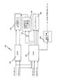
図4は、並列分散機能TLB構造を採用するコンピュータマイクロアーキテクチャ250を示す。コンピュータマイクロアーキテクチャ250は、整数ロード命令ではない命令によって必要とされるエントリにより小型TLBをスラッシュしないことによって高速整数ロードデータアクセスに対し、小型TLBを効率よく使用できるようにする。マイクロアーキテクチャ250は、小型TLBにおけるスラッシングを減少させることによって事前検査済みキャッシュタグ設計のキャッシュデータ無効化を減少させ、減少したメモリポートの帯域を提供して、小型(整数ロードデータ)TLBの設計をより小型かつ高速にする。マイクロアーキテクチャ250は、より大型キャッシュにある浮動小数点アプリケーション等大型データ構造に対処するためにより大型のTLBを提供し、かつ、浮動小数点アプリケーションの大きい帯域幅の必要性に対処するために大きい帯域幅のTLBを提供する。また、マイクロアーキテクチャ250は、高速整数データキャッシュを中断(disrupt)することなくストアおよび無効化の要求変換を処理する方法も提供する。最後に、マイクロアーキテクチャ250は、アドレス指定するための例外および保護コントロールに単一の位置を提供するが、これは、整数ロードデータキャッシュにおいて、小型TLBとは別のものである。
【0032】
コンピュータマイクロアーキテクチャ250は、整数ロードデータTLB(L0TLB)252と、マスタTLB(DTLB)254とからなる並列TLBを含む。また、マイクロアーキテクチャ250は、整数ロードデータキャッシュ(L0D)264、L1データキャッシュ266、および並列物理タグ検索を有するストア/無効化コントロール262も含む。図4に示すように、TLBは、4個のメモリポート0〜3を介してアクセスされる。しかしながら、マイクロアーキテクチャ250は、この構成に制限されるものではなく、任意の数のメモリポートがTLBにアクセスできる。
【0033】
L0TLB252は、整数ロードデータに短いレイテンシーを提供するように設計される。これを達成するために、L0TLB252にはいくつかの制限が加えられる。図4に示す例では、4個のメモリポートの2個のみがL0TLB252にアクセスすることを許されて、L0TLB252のサイズおよび複雑性を低減させ、従ってその速度が増加する。この低減は、整数ロードを4個のメモリポートの2個にのみ割り当てることによって可能である。さらに、整数ストア命令は、L0TLB252にアクセスしないが、DTLB254において処理される。この構成は、マイクロアーキテクチャ250がL0TLB252においてロード専用TLBエントリを割り付けることを可能とし、TLBエントリのスラッシングを低減させ、事前検査済みタグキャッシュ設計においてはキャッシュラインを無効化するという副作用を有する。
【0034】
次に、浮動小数点ロードおよびストアならびにその他の様々なTLBアクセス命令は、L0TLB252にアクセスしなくてもよく、L0TLB252におけるTLBエントリのスラッシングを低減させる。浮動小数点アクセスは、L1データキャッシュ266により処理され、DTLB254を介して変換される。
【0035】
例外および保護の情報は、L0TLB252に含まれないため、より小型でより高速の設計が可能になる。整数ロード命令は、例外および保護情報がDTLB254にのみ存在することから、L0TLB252とDTLB254の両方において、処理されるべき有効キャッシュヒットのエントリを有する。最後に、すべての整数ロード命令を検索してキャッシュヒットを決定するためのパスが、L0TLB252からL0D264まで提供される。
【0036】
DTLB254は、大量のTLBエントリを提供し、かつL0TLB252の場合より長いレイテンシーを有する大きい帯域幅を提供するように設計される。DTLB254は、すべてのTLBアクセスにパラレルポートを提供して、1サイクルにつき4つのメモリ動作の実行を支援するための大きい帯域幅を提供する。しかしながら、上述したように、マイクロアーキテクチャ250は、4個のメモリポートに制限されるものではない。また、DTLB254は、各メモリポートがロードまたはストアをサービスできるように汎用メモリポートをさらに提供する。L0D264は、1サイクルにつき2個のロードまたは2個のストアに制限され、高速のレイテンシーを提供するので、DTLB254は、1サイクルあたり最大4個の浮動小数点ロードまたは最大4個の浮動小数点ストアの実行を可能にする。
【0037】
DTLB254は、すべての4個のメモリポートに例外および保護の情報を提供する。これにより、この情報を必要とすることなく、L0TLB252がより小型かつ高速になるようにL0TLB252を構成することができる。DTLB254は、整数データパスに対する変換パスを、ストアアドレス更新およびキャッシュライン無効化機能に提供する。最後に、DTLB254は、L1データキャッシュ266に対するパスを提供し、すべての浮動小数点ロードおよびストア動作についてキャッシュ検索を実行する。
【0038】
マイクロアーキテクチャ250において、整数ストア更新アドレスおよび無効化アドレスがL0D264に提供されてもよい。コントロール262により、マイクロアーキテクチャ250は、キャッシュラインの物理アドレスを、事前検査済みキャッシュタグエントリと並列で記憶することができる。さらに、パス261がDTLB254からストア更新およびストア無効化の整数データパスまで、提供される。DTLB254アドレスは、物理アドレスキャッシュタグ構造におけるあらゆる方式の連想性(associativity)と比較され、どの方式の連想性が現在のストアまたは無効化要求に一致するかを検出する。コントロール262により、事前検査済みタグキャッシュL0D264の有効状態が無効化要求に応じて更新され、整数ストア動作に応じて整数ロードデータキャッシュを更新する。最後に、例外情報モジュール268は、4個のメモリポート0〜3すべてについてDTLB254からの例外情報を受信する。
【0039】
以上、例示および説明の目的で、機能が並列に分散された変換索引バッファについて説明してきた。本記載は、これをもってすべてとするものでもなければ、本発明を開示される厳密な形式に制限するものでもなく、上記の教示に照らして他の修正および変形も可能である。本記載は、機能が並列に分散された変換索引バッファおよびその実用的な適用の原理を説明することで、当業者が、企図された特定用途に適合される各種実施態様および修正案において最もよく使用できるようにしたものである。
【0040】
本発明を要約すると次のようになる。コンピュータシステムにおいて、機能が並列に分散された変換索引バッファ(TLB)は、小型で高速のTLB(252)及び大型であるがより低速の別のTLB(254)を含む。2つのTLBは並列に動作する。小型のTLB(252)は整数ロードデータを受信し、大型のTLB(254)は他の仮想アドレス情報を受信する。2つのTLB間において、ロードとストア命令、整数と浮動小数点命令等の機能を分散することにより、小型のTLBは短いレイテンシーで動作でき、スラッシング及び類似の問題を回避する一方、大型のTLBはメモリの集約的な動作に対して、大きい帯域幅を提供する。この機構は、事前検査済みキャッシュタグ設計に特に有用である並列ストア更新および無効化機構(262)も提供する。
【0041】
以下においては、本発明の種々の構成要件の組み合わせからなる例示的な実施態様を示す。
1.第1のデータを受信するように適合される第1の変換索引バッファ(TLB)(252)と、
前記第1のTLB(252)と並列な第2のTLB(254)であって、前記第1のデータを受信し、かつ前記第1のTLBにおいて前記第1のデータの受信と並列に第2のデータを受信するように適合される第2のTLB(254)と、
を含むコンピュータマイクロアーキテクチャ。
2.前記第1のデータが整数ロードデータからなり、前記第2のデータは、整数ストアデータ、浮動小数点ロードまたはストアデータ、TLB参照および更新命令、ならびに例外およびキャッシュミスのための整数ロードデータの1つ以上を含む、上記1記載のコンピュータマイクロアーキテクチャ。
3.第1のキャッシュ(264)と、
第2のキャッシュ(266)とをさらに含み、
前記第1のTLB(252)が、受信した第1のデータに基づいてTLBヒット情報を提供し、前記第1のキャッシュ(264)が、前記TLBヒット情報を保有し、
前記第2のTLB(254)が物理アドレス情報を提供し、前記第2のキャッシュ(266)が、前記物理アドレス情報を保有する、上記1記載のコンピュータマイクロアーキテクチャ。
4.事前検査済みキャッシュタグエントリの物理アドレスを保持するコントロール(262)をさらに含む、上記1記載のコンピュータマイクロアーキテクチャ。5.前記第1のTLB(252)は、第1および第2のメモリポートによってアクセスされ、前記第2のTLB(254)は、前記第1および第2のメモリポート、ならびに第3および第4のメモリポートによってアクセスされ、かつ前記第2のTLB(254)は、例外および特権の情報を記憶する、上記1記載のコンピュータマイクロアーキテクチャ。
6.事前検査済みタグキャッシュを有するコンピュータマイクロアーキテクチャにおいて、
整数ロードTLB(252)と、
前記整数ロードTLB(252)と並列に動作するマスタTLB(254)であって、整数ロードが前記整数ロードTLBに供給され、かつロードおよびストアが前記マスタTLB(254)に提供される、マスタTLB(254)と、
前記整数ロードTLB(252)からの出力を受信する整数ロードデータキャッシュ(264)と、及び
前記マスタTLB(254)からの出力を受信するデータキャッシュ(266)であって、前記整数ロードTLBが、仮想アドレスに基づいてTLBヒット情報を提供するとともに、前記整数ロードデータキャッシュが前記TLBヒット情報を記憶し、かつ前記マスタTLBが、物理アドレスを前記データキャッシュに提供するとともに、前記データキャッシュが前記物理アドレスを保持する、データキャッシュ(266)と、
を含む変換索引バッファ(TLB)構造。
7.前記マスタTLB(254)および前記整数ロードデータキャッシュ(264)に結合され、前記整数ロードデータキャッシュのキャッシュラインに更新信号または無効化信号を提供する、ストア更新および無効化コントロール(262)と、及び
前記マスタTLBが例外および特権の情報を受信する、例外および特権の情報モジュール(268)と、
をさらに含む、前記6記載の変換索引バッファ(TLB)構造。
8.コンピュータシステムにおける仮想アドレス情報変換の方法であって、
第1の変換索引バッファ(TLB)(252)において第1の仮想アドレス情報を受信するステップと、及び
同時に、第2のTLB(254)において第2の仮想アドレス情報を受信するステップとを含む方法。
9.前記第1の仮想アドレス情報は整数ロード情報からなり、前記第2の仮想アドレス情報は、整数ストアデータ、浮動小数点ロードおよびストアデータ、ならびにTLB参照および更新命令の1つ以上を含む、上記8記載の方法。
10.前記第1の仮想アドレス情報をTLBヒット情報に変換するステップと、
前記TLBヒット情報を第1のキャッシュに提供するステップと、
前記第2の仮想アドレス情報を物理アドレス情報に変換するステップと、
前記物理アドレス情報を前記第1のキャッシュおよび第2のキャッシュに提供するステップと、
前記第2のTLBに例外および特権の情報を記憶するステップと、
をさらに含む、上記8記載の方法。
【0042】
【発明の効果】
本発明により、変換索引バッファを有するキャッシュにおいて、キャッシュヒットのためのアクセス時間が最適化され、コンピュータシステムの性能が改善される。
【図面の簡単な説明】
【図1】従来技術のキャッシュ構造を示す。
【図2】従来技術のキャッシュ構造を示す。
【図3】事前検査済みタグキャッシュを有するコンピュータシステムを示す。
【図4】図3の事前検査済みタグキャッシュとともに使用される並列分散型変換索引バッファ構造を示す。
【符号の説明】
250 コンピュータマイクロアーキテクチャ
252 整数ロードTLB(L0TLB)
254 マスタTLB(DTLB)
262 ストア/無効化コントロール
264 整数ロードデータキャッシュ(L0D)
266 L1データキャッシュ[0001]
BACKGROUND OF THE INVENTION
The technical field to which this invention pertains includes computer systems that use translation index buffers for prevalidated cache tag design.
[0002]
[Prior art]
Computer systems use a multi-level hierarchical memory system. The multi-level hierarchy memory system is relatively fast and expensive for the top level hierarchy, but is limited in capacity, but is relatively slow and low cost for the bottom level hierarchy. It has a hierarchical structure that leads to a memory with a large capacity. The hierarchy can include a small, fast memory called a cache for speed, either physically integrated within the processor or physically attached in close proximity to the processor. The computer system may employ an instruction cache and a data cache separately. Further, the computer system can use a multi-level cache. Since the use of the cache is transparent to the computer program at the instruction level, it can be added to the computer architecture without changing the instruction set or requiring modifications to existing programs.
[0003]
If the processor requests an item from the cache and the item exists in the cache, a cache hit occurs. On the other hand, if the processor requests an item from the cache and the item does not exist in the cache, a cache miss occurs. In the case of a cache miss, the processor retrieves the requested item from a lower level memory hierarchy. In many processor designs, the time it takes to access an item due to a cache hit is a major factor in the processor clock rate if the designer seeks a single cycle cache access time. One of the limiters. In other designs, the cache access time may be multiple cycles, but the processor performance can be improved in most cases where the cache access time per cycle is reduced. Therefore, optimizing access time for cache hits is important for the performance of the computer system.
[0004]
Cache design is linked to the concept of virtual storage. Virtual storage systems allow computer programmers to think of memory as a single level, constant single storage unit, but in practice, between the auxiliary storage and the fast storage (cache) on the page A dynamic address translation unit is provided that automatically moves program blocks on demand.
[0005]
The cache design is also associated with the concept of fully associative or content addressable memory (CAM). In addition to having a traditional hardware built-in addressing mechanism, the content-specific memory allows comparison with the desired bit position so that all entries can be specified and matched simultaneously during one memory cycle time. It is a random access memory that also has hardware built-in logic. Therefore, since the entry can be accessed by using a part of the contents, there is no need to know the specific address of the desired entry. All entries that match the specified bit position are flagged and can be addressed in the current or subsequent memory cycle.
[0006]
The memory may be organized into words (eg, 32 bits or 64 bits per word). The minimum amount of memory that can be transferred between the cache and the next lower level memory hierarchy is called a line or block. One line may be a plurality of words (eg, 16 words / line). Also, the memory may be divided into pages or segments so that each page has a number of lines. Depending on the computer system, the page size may be variable.
[0007]
In today's computer memory architecture, a central processing unit (CPU) generates virtual addresses that are converted to physical addresses by a combination of hardware and software. The physical address is used to access the physical main memory. A group of virtual addresses can be dynamically assigned to each page. Virtual memory requires a data structure, sometimes called a page table, that translates virtual addresses into physical addresses. In order to shorten the address translation time, the computer may use a special associative cache dedicated to an address location called a translation lookaside buffer (TLB).
[0008]
A cache can include multiple segments or ways. A cache is fully associative if it stores the entire line address along with the data and can place any line anywhere in the cache. For large caches where any line can be placed anywhere, the hardware required to quickly determine if and where an item is in the cache can be very large and expensive. is there. The larger the cache, the faster and space-saving alternatives use a subset of addresses (called indexes) to specify line locations in the cache, and then the rest of the higher bits of each physical address called a tag Is stored with the data. In an indexing cache, an item with a specific address can only be placed within a set of lines specified by the index. A cache is said to be a direct mapping expression if the cache is configured so that the index at a given address maps exactly to one line in the subset or way. A cache is said to be set associative if the index maps to more than one line in a subset or way. Some or all of the addresses may be hashed to provide a set index that divides the address space into sets.
[0009]
In direct mapping, when a line is requested, only one line in the cache has a matching index bit. Thus, the data can be immediately retrieved and sent to the data bus before the computer system determines whether the rest of the addresses match. The data may be valid or invalid, but in the normal case where the data is valid, the data bits are available on the data bus before the computer system determines validity. In a set associative cache, the computer system does not know which line corresponds to an address until it compares the complete address. That is, in the set associative cache, the comparison result of the tag is used to select which line of data bits in one set of lines is supplied to the processor.
[0010]
[Problems to be solved by the invention]
In a cache with a TLB, the critical timing path for hits requires the following four sequences of operations: That is, 1) It is necessary to present the virtual tag to the CAM in the TLB and determine the position of the corresponding physical tag in the random access memory (RAM) of the TLB. 2) Next, the physical tag is retrieved from the TLB random access memory. 3) Next, the physical tag from the TLB RAM needs to be compared with the physical tag accessed from the tag section of the cache, and 4) the appropriate data line needs to be selected. This sequence of four operations is required to read the cache and can be a limiter on processor frequency and processor performance.
[0011]
[Means for Solving the Problems]
The pre-checked tag cache holds hit information from the translation index buffer (TLB) instead of address information as in conventional practice. That is, when a virtual address is provided to the TLB instead of being provided as an output from the TLB, a TLB hit bit is provided. The TLB hit bit is then compared to a pre-checked cache tag (which has TLB hit information) to determine whether a cache hit or a cache miss has occurred. In order to increase the processing speed, the TLB may be reduced to 32 entries, for example. The TLB is used for operations with a short required latency, such as integer load operations.
[0012]
Small TLB presents the potential problem of, for example, thrashing, which reduces cache performance, ie, swapping out pages or TLB entries. Since the TLB is small, TLB entries can be eliminated very quickly, effectively losing data from the cache. That is, since the pre-inspected cache tag includes TLB hit information and does not include a physical address, if the TLB entry changes, the hit information is no longer valid and any data associated with the older TLB entry is lost. Is called.
[0013]
In this microarchitecture, a separate large TLB may be added to a process operation that can handle a longer latency, such as a store operation, in order to prevent TLB thrashing while keeping the TLB entry small. This large TLB can also provide greater bandwidth, for example, for floating point operations. For example, the TLB entries required in the small TLB may be limited to those required for integer loads, and all other TLB entries may be forwarded to the large TLB. TLBs operate in parallel. In addition, all exception and privilege checks may be performed on the large TLB, which also has the effect of reducing the integer load access time. Using this parallel TLB architecture has the added benefit of reducing pipeline outages that can occur when small and large TLBs are accessed in series.
[0014]
As a further result of a cache tag having only TLB hit information instead of a physical address, a mechanism for updating and invalidating cache lines may be provided. In this mechanism, a parallel structure can be provided that searches, updates and / or invalidates cache lines separately from the small TLB mechanism and the integer load data path. Further, in some situations, a simple physical address is provided in the data cache. In order to find an appropriate cache line, a control is provided that includes a tag with a physical address and a physical address that bypasses around the large TLB, based solely on the physical address.
[0015]
DETAILED DESCRIPTION OF THE INVENTION
The parallel distributed function conversion index buffer will be described below with reference to the drawings. In the drawings, like reference numerals denote like elements.
[0016]
A cache with a TLB that does not need to retrieve physical tags from the TLB can improve the overall critical path time to access a cache with a TLB. In such a design, instead of storing the physical tag in the cache, the cache stores the location in the TLB where the physical tag is stored. A TLB can include more than one CAM. In a cache hit, one of the CAMs in the TLB can generate a vector that specifies the location in the TLB where the physical address is stored. This vector may be compared to a position vector stored in the cache. The position vector comparison provides enough information to allow the selection of one data line in a set without having to actually retrieve the physical address. As a result, an operation that consumes a considerable amount of time (physical address search) is eliminated from the critical time path of the cache hit. Furthermore, by comparing position vectors rather than physical tags, it is possible to use comparison logic that is faster and simpler than conventional digital comparators.
[0017]
FIG. 1 shows an example of a prior art cache.
[0018]
FIG. 2 shows another prior art cache. A 4-way set associative cache is used for illustration. The
[0019]
FIG. 3 shows a computer microarchitecture with a 4-way set
[0020]
Further details regarding the pre-inspected cache architecture are presented in copending US patent application Ser. No. 08 / 955,821, entitled “CACHE MEMORY WITH REDUCED ACCESS TIME”, filed Oct. 22, 1997. Yes. The disclosure of which is hereby incorporated by reference.
[0021]
In the
[0022]
For cache access, the
[0023]
For cache access,
[0024]
In
[0025]
The microarchitecture shown in FIG. 3 includes a pre-validated tag cache. The pre-check puts a limit on how the TLB in the microarchitecture works when the computer microarchitecture designer attempts to maximize the total bandwidth while minimizing cache load latency. For example, pre-inspected tag caches provide very fast access times for specific loads, but microarchitecture designers limit the translation between virtual and physical addresses, and within different cache levels You may choose to limit the distribution of these processes. The microarchitecture may, for example, provide a fast integer load and a large bandwidth floating point load. That is, the integer load data needs to have a high-speed access time, but its operation setting size is generally small. To optimize integer load latency, some processors provide a small but fast first level cache. To provide virtual address translation and to avoid address aliasing problems, some processors access the TLB and check with a cache tag to determine if data is in the cache Some need to provide a physical address. For the purpose of fast integer data access, the TLB size may be limited to a minimum number of entries (16-32, etc.) to reduce memory latency. This conflicts with the large number of entries required on a processor with a large cache structure that may require more than 256 TLB entries.
[0026]
In the pre-checked cache tag system as shown in FIG. 3, the TLB entry is logically used in the cache tag to identify the cache line. When a TLB entry is removed, controls are typically used to invalidate all data in the pre-checked cache tag associated with the removed TLB entry. However, this action can delay processing because one TLB entry can be mapped to most or all of the data cache. Thus, the TLB does not support program execution, but can continuously swap pages (ie, thrash) pages into and out of memory.
[0027]
The performance of floating point data processing is usually limited by the memory bandwidth to and from the floating point execution unit. In contrast to integer load data accesses that require short latencies, floating point accesses can usually be scheduled, thus increasing the latency period. Similarly, integer data sizes are usually small, but floating point data sets are usually very large. Ideally, the TLB operation of the floating point load / store operation provides both large bandwidth and large data space conversion (large number of TLB entries accessed). One design provides full bandwidth for all memory ports and a large but slow TLB for conversion of floating point requests. Furthermore, the use of memory ports may be unrestricted, allowing for more load and store combinations.
[0028]
Storage in the pre-inspected integer load data cache or invalidation of this data cache is difficult because the physical address of the cache line is not available in the cache tag, but this is because the cache tag has pre-inspected TLB hit information. It is because it is only holding. In addition, the small integer load data cache TLB is not used for store translation because the TLB is smaller (eg, 16 or 32 entries) than the need for fast latency. One option is to separate store TLB accesses to larger and slower TLBs, store operations that may not be performed in the first level cache (such as floating point stores), and other such as flash cache, bus snoop, etc. To provide a mechanism for invalidating the pre-inspected integer load cache for the invalidation operation.
[0029]
Many computer instructions such as TLB support instructions, including floating point loads and stores, purges, inserts and probes, integer stores, do not require immediate access to the fast integer data cache. Some of the computer instructions may not have data in the fast integer load cache to avoid smaller cache thrashing. In order to support better use of the fast integer data cache, a mechanism may be provided to prevent this type of data from loading the integer data cache. Because these instructions can bypass the integer cache, all exception information is stored only in the large TLB, which includes, for example, all store operations, floating point loads, or TLB references (reads) and update instructions. It may be necessary to access only with the TLB support instruction.
[0030]
Finally, by passing all instructions through the first level TLB (which needs to be small for high speed), the TLB miss rate increases, so the pipeline stalls in the processor. May occur. Thus, the microarchitecture shown in FIG. 3 may be adapted to use a parallel TLB structure that reduces TLB miss rates and pipeline outages.
[0031]
FIG. 4 shows a
[0032]
The
[0033]
L0TLB252 is designed to provide short latency for integer load data. In order to achieve this, some restrictions are placed on L0TLB252. In the example shown in FIG. 4, only two of the four memory ports are allowed to access
[0034]
Next, floating point load and store and various other TLB access instructions may not access
[0035]
Since exception and protection information is not included in L0TLB252, a smaller and faster design is possible. The integer load instruction has entries for valid cache hits to be processed in both
[0036]
[0037]
The
[0038]
In
[0039]
In the foregoing, for the purposes of illustration and description, a translation index buffer having functions distributed in parallel has been described. This description is not intended to be exhaustive or to limit the invention to the precise form disclosed, and other modifications and variations are possible in light of the above teaching. This description explains the principles of the translation index buffer and its practical application in which functions are distributed in parallel, so that those skilled in the art are best in various implementations and proposed modifications adapted to the intended specific use. It can be used.
[0040]
The present invention is summarized as follows. In a computer system, a translation index buffer (TLB) with functions distributed in parallel includes a small and fast TLB (252) and another large but slower TLB (254). The two TLBs operate in parallel. The small TLB (252) receives integer load data, and the large TLB (254) receives other virtual address information. By distributing functions such as load and store instructions, integer and floating point instructions between two TLBs, small TLBs can operate with short latency, avoiding thrashing and similar problems, while large TLBs are memory Provides a large bandwidth for the intensive operation of This mechanism also provides a parallel store update and invalidation mechanism (262) that is particularly useful for pre-checked cache tag designs.
[0041]
In the following, exemplary embodiments consisting of combinations of various constituents of the present invention are shown.
1. A first translation index buffer (TLB) (252) adapted to receive the first data;
A second TLB (254) in parallel with the first TLB (252) for receiving the first data and receiving a second in parallel with the reception of the first data in the first TLB; A second TLB (254) adapted to receive the data of
Including computer microarchitecture.
2. The first data comprises integer load data, and the second data is one of integer store data, floating point load or store data, TLB reference and update instructions, and integer load data for exceptions and cache misses. The computer microarchitecture according to 1 above, including the above.
3. A first cache (264);
A second cache (266),
The first TLB (252) provides TLB hit information based on the received first data, and the first cache (264) holds the TLB hit information,
The computer microarchitecture of
4). The computer microarchitecture of
6). In a computer microarchitecture with a pre-inspected tag cache,
Integer load TLB (252),
A master TLB (254) operating in parallel with the integer load TLB (252), wherein an integer load is provided to the integer load TLB, and loads and stores are provided to the master TLB (254) (254)
An integer load data cache (264) for receiving output from the integer load TLB (252); and
A data cache (266) that receives an output from the master TLB (254), wherein the integer load TLB provides TLB hit information based on a virtual address, and the integer load data cache includes the TLB hit information A data cache (266), wherein the master TLB provides a physical address to the data cache and the data cache holds the physical address;
A translation index buffer (TLB) structure containing
7). A store update and invalidation control (262) coupled to the master TLB (254) and the integer load data cache (264) and providing an update signal or invalidation signal to a cache line of the integer load data cache; and
An exception and privilege information module (268), wherein the master TLB receives exception and privilege information;
The transform index buffer (TLB) structure of claim 6, further comprising:
8). A method of virtual address information conversion in a computer system, comprising:
Receiving first virtual address information at a first translation index buffer (TLB) (252); and
Simultaneously receiving second virtual address information in a second TLB (254).
9. 9. The 8 above, wherein the first virtual address information comprises integer load information, and the second virtual address information includes one or more of integer store data, floating point load and store data, and TLB reference and update instructions. the method of.
10. Converting the first virtual address information into TLB hit information;
Providing the TLB hit information to a first cache;
Converting the second virtual address information into physical address information;
Providing the physical address information to the first cache and a second cache;
Storing exception and privilege information in the second TLB;
The method according to 8 above, further comprising:
[0042]
【The invention's effect】
The present invention optimizes access time for cache hits and improves computer system performance in a cache with a translation index buffer.
[Brief description of the drawings]
FIG. 1 illustrates a prior art cache structure.
FIG. 2 illustrates a prior art cache structure.
FIG. 3 illustrates a computer system having a pre-validated tag cache.
FIG. 4 illustrates a parallel distributed translation index buffer structure used with the pre-checked tag cache of FIG.
[Explanation of symbols]
250 computer microarchitecture
252 integer load TLB (L0TLB)
254 Master TLB (DTLB)
262 Store / Disable Control
264 Integer load data cache (L0D)
266 L1 data cache
Claims (3)
整数ロードデータを受信するように適合された整数ロード変換索引バッファ(TLB)と、及び
前記整数ロードTLBと並列に接続され、前記整数ロードデータを受信し、かつ前記整数ロードTLBにおける前記整数ロードデータの受信と並列に、整数ストアデータ、浮動小数点ロードまたはストアデータ、及びTLB参照命令および更新命令のうちの1つ又は複数を受信するように適合されたマスタTLBとを含み、
前記整数ロードTLBが、第1および第2のメモリポートによってアクセスされ、前記マスタTLBが、前記第1および第2のメモリポート、ならびに第3および第4のメモリポートによってアクセスされる、コンピュータマイクロアーキテクチャ。A computer microarchitecture,
An integer load transform index buffer (TLB) adapted to receive integer load data; and connected in parallel with the integer load TLB, receiving the integer load data, and the integer load data in the integer load TLB In parallel with receiving a master TLB adapted to receive one or more of integer store data , floating point load or store data, and TLB reference and update instructions ;
A computer microarchitecture in which the integer load TLB is accessed by first and second memory ports, and the master TLB is accessed by the first and second memory ports and third and fourth memory ports. .
データセクションとタグセクションを有する整数ロードデータキャッシュであって、当該データセクションに格納されているキャッシュデータの、物理タグの、前記整数ロードTLBにおける位置を示す物理TLBヒットを当該タグセクションに保持し、前記整数ロードTLBから提供される前記仮想TLBヒットと前記タグセクションに保持されている前記物理TLBヒットとを用いてヒット判定を行う整数ロードデータキャッシュと、
前記整数ロードTLBと並列に動作し、ロード及びストアのための仮想アドレスが供給されるマスタTLBであって、当該仮想アドレスに対応する仮想タグのための物理タグを提供するマスタTLBと、
データセクションとタグセクションを有するデータキャッシュであって、当該データセクションに格納されているキャッシュデータの物理タグを当該タグセクションに保持し、前記マスタTLBから提供される物理タグと当該タグセクションに保持されている物理タグとを用いてヒット判定を行うデータキャッシュとを含む、装置。 An integer load TLB to which a virtual address for integer loading is supplied, the integer loading TLB providing a virtual TLB hit indicating the position of the virtual tag corresponding to the virtual address in the integer load TLB;
An integer load data cache having a data section and a tag section, the physical TLB hit indicating the position of the physical tag of the cache data stored in the data section in the integer load TLB is held in the tag section; An integer load data cache that performs a hit determination using the virtual TLB hit provided from the integer load TLB and the physical TLB hit held in the tag section;
A master TLB that operates in parallel with the integer load TLB and is supplied with virtual addresses for load and store , and provides a physical tag for a virtual tag corresponding to the virtual address ;
A data cache having a data section and a tag section , wherein a physical tag of cache data stored in the data section is held in the tag section, and is held in the physical tag and the tag section provided from the master TLB. And a data cache that performs hit determination using a physical tag .
Applications Claiming Priority (2)
| Application Number | Priority Date | Filing Date | Title |
|---|---|---|---|
| US09/466,494 US6625714B1 (en) | 1999-12-17 | 1999-12-17 | Parallel distributed function translation lookaside buffer |
| US09/466494 | 1999-12-17 |
Publications (3)
| Publication Number | Publication Date |
|---|---|
| JP2001195303A JP2001195303A (en) | 2001-07-19 |
| JP2001195303A5 JP2001195303A5 (en) | 2005-07-07 |
| JP4065660B2 true JP4065660B2 (en) | 2008-03-26 |
Family
ID=23851970
Family Applications (1)
| Application Number | Title | Priority Date | Filing Date |
|---|---|---|---|
| JP2000379986A Expired - Fee Related JP4065660B2 (en) | 1999-12-17 | 2000-12-14 | Translation index buffer with distributed functions in parallel |
Country Status (2)
| Country | Link |
|---|---|
| US (2) | US6625714B1 (en) |
| JP (1) | JP4065660B2 (en) |
Families Citing this family (27)
| Publication number | Priority date | Publication date | Assignee | Title |
|---|---|---|---|---|
| US6625714B1 (en) * | 1999-12-17 | 2003-09-23 | Hewlett-Packard Development Company, L.P. | Parallel distributed function translation lookaside buffer |
| US6907600B2 (en) * | 2000-12-27 | 2005-06-14 | Intel Corporation | Virtual translation lookaside buffer |
| US6820170B1 (en) * | 2002-06-24 | 2004-11-16 | Applied Micro Circuits Corporation | Context based cache indexing |
| US20040054867A1 (en) * | 2002-09-13 | 2004-03-18 | Paulus Stravers | Translation lookaside buffer |
| US7234034B2 (en) * | 2002-09-16 | 2007-06-19 | Texas Instruments Incorporated | Self-clocking memory device |
| US7243208B2 (en) * | 2003-08-13 | 2007-07-10 | Renesas Technology Corp. | Data processor and IP module for data processor |
| US7225316B2 (en) * | 2003-11-17 | 2007-05-29 | Intel Corporation | Memory mapping apparatus, systems, and methods |
| US20060224857A1 (en) * | 2005-03-29 | 2006-10-05 | O'connor Dennis M | Locking entries into translation lookaside buffers |
| US20070094476A1 (en) * | 2005-10-20 | 2007-04-26 | Augsburg Victor R | Updating multiple levels of translation lookaside buffers (TLBs) field |
| JP2007233615A (en) * | 2006-02-28 | 2007-09-13 | Fujitsu Ltd | Address conversion device |
| US8185716B2 (en) * | 2007-10-22 | 2012-05-22 | Qimonda Ag | Memory system and method for using a memory system with virtual address translation capabilities |
| US8015386B1 (en) * | 2008-03-31 | 2011-09-06 | Xilinx, Inc. | Configurable memory manager |
| US8099580B2 (en) * | 2009-06-09 | 2012-01-17 | Freescale Semiconductor, Inc | Translation look-aside buffer with a tag memory and method therefor |
| US8255629B2 (en) * | 2009-06-22 | 2012-08-28 | Arm Limited | Method and apparatus with data storage protocols for maintaining consistencies in parallel translation lookaside buffers |
| US8181131B2 (en) | 2010-04-30 | 2012-05-15 | International Business Machines Corporation | Enhanced analysis of array-based netlists via reparameterization |
| US8146034B2 (en) | 2010-04-30 | 2012-03-27 | International Business Machines Corporation | Efficient Redundancy Identification, Redundancy Removal, and Sequential Equivalence Checking within Designs Including Memory Arrays. |
| US8566764B2 (en) | 2010-04-30 | 2013-10-22 | International Business Machines Corporation | Enhanced analysis of array-based netlists via phase abstraction |
| US8478574B2 (en) | 2010-04-30 | 2013-07-02 | International Business Machines Corporation | Tracking array data contents across three-valued read and write operations |
| US8336016B2 (en) | 2010-05-07 | 2012-12-18 | International Business Machines Corporation | Eliminating, coalescing, or bypassing ports in memory array representations |
| US8307313B2 (en) | 2010-05-07 | 2012-11-06 | International Business Machines Corporation | Minimizing memory array representations for enhanced synthesis and verification |
| US8291359B2 (en) | 2010-05-07 | 2012-10-16 | International Business Machines Corporation | Array concatenation in an integrated circuit design |
| WO2013058745A1 (en) | 2011-10-18 | 2013-04-25 | Soft Machines, Inc. | Methods and systems for managing synonyms in virtually indexed physically tagged caches |
| US20130179642A1 (en) * | 2012-01-10 | 2013-07-11 | Qualcomm Incorporated | Non-Allocating Memory Access with Physical Address |
| US9311239B2 (en) | 2013-03-14 | 2016-04-12 | Intel Corporation | Power efficient level one data cache access with pre-validated tags |
| US10776281B2 (en) * | 2018-10-04 | 2020-09-15 | International Business Machines Corporation | Snoop invalidate filter for distributed memory management unit to reduce snoop invalidate latency |
| US11580031B2 (en) * | 2019-07-31 | 2023-02-14 | Intel Corporation | Hardware for split data translation lookaside buffers |
| US11061828B1 (en) * | 2020-02-25 | 2021-07-13 | International Business Machines Corporation | Using multi-tiered cache to satisfy input/output requests |
Family Cites Families (9)
| Publication number | Priority date | Publication date | Assignee | Title |
|---|---|---|---|---|
| US5412787A (en) * | 1990-11-21 | 1995-05-02 | Hewlett-Packard Company | Two-level TLB having the second level TLB implemented in cache tag RAMs |
| US5644748A (en) * | 1992-01-30 | 1997-07-01 | Fujitsu Limited | Processor system including an index buffer circuit and a translation look-aside buffer control circuit for processor-to-processor interfacing |
| JP3740195B2 (en) * | 1994-09-09 | 2006-02-01 | 株式会社ルネサステクノロジ | Data processing device |
| US5860017A (en) | 1996-06-28 | 1999-01-12 | Intel Corporation | Processor and method for speculatively executing instructions from multiple instruction streams indicated by a branch instruction |
| US5859999A (en) | 1996-10-03 | 1999-01-12 | Idea Corporation | System for restoring predicate registers via a mask having at least a single bit corresponding to a plurality of registers |
| US6014732A (en) * | 1997-10-22 | 2000-01-11 | Hewlett-Packard Company | Cache memory with reduced access time |
| US6351797B1 (en) * | 1997-12-17 | 2002-02-26 | Via-Cyrix, Inc. | Translation look-aside buffer for storing region configuration bits and method of operation |
| US6272597B1 (en) * | 1998-12-31 | 2001-08-07 | Intel Corporation | Dual-ported, pipelined, two level cache system |
| US6625714B1 (en) * | 1999-12-17 | 2003-09-23 | Hewlett-Packard Development Company, L.P. | Parallel distributed function translation lookaside buffer |
-
1999
- 1999-12-17 US US09/466,494 patent/US6625714B1/en not_active Expired - Fee Related
-
2000
- 2000-12-14 JP JP2000379986A patent/JP4065660B2/en not_active Expired - Fee Related
-
2003
- 2003-08-27 US US10/648,405 patent/US6874077B2/en not_active Expired - Lifetime
Also Published As
| Publication number | Publication date |
|---|---|
| US6874077B2 (en) | 2005-03-29 |
| JP2001195303A (en) | 2001-07-19 |
| US6625714B1 (en) | 2003-09-23 |
| US20040039893A1 (en) | 2004-02-26 |
Similar Documents
| Publication | Publication Date | Title |
|---|---|---|
| JP4065660B2 (en) | Translation index buffer with distributed functions in parallel | |
| US6772316B2 (en) | Method and apparatus for updating and invalidating store data | |
| US6014732A (en) | Cache memory with reduced access time | |
| US8984254B2 (en) | Techniques for utilizing translation lookaside buffer entry numbers to improve processor performance | |
| US4332010A (en) | Cache synonym detection and handling mechanism | |
| US6493812B1 (en) | Apparatus and method for virtual address aliasing and multiple page size support in a computer system having a prevalidated cache | |
| EP0856798B1 (en) | A cache system | |
| US6532528B1 (en) | Data processor and data processor system having multiple modes of address indexing and operation | |
| US5586283A (en) | Method and apparatus for the reduction of tablewalk latencies in a translation look aside buffer | |
| US5623627A (en) | Computer memory architecture including a replacement cache | |
| KR920005280B1 (en) | High speed cache system | |
| US6161166A (en) | Instruction cache for multithreaded processor | |
| US4797814A (en) | Variable address mode cache | |
| US5668968A (en) | Two-level virtual/real set associative cache system and method with improved synonym detection | |
| US7136967B2 (en) | Multi-level cache having overlapping congruence groups of associativity sets in different cache levels | |
| JP3666689B2 (en) | Virtual address translation method | |
| US5715427A (en) | Semi-associative cache with MRU/LRU replacement | |
| US6356990B1 (en) | Set-associative cache memory having a built-in set prediction array | |
| KR20010101695A (en) | Techniques for improving memory access in a virtual memory system | |
| US5737575A (en) | Interleaved key memory with multi-page key cache | |
| JP3431878B2 (en) | Instruction cache for multithreaded processors | |
| JP3210637B2 (en) | Method and system for accessing a cache memory in a data processing system | |
| JP2000339221A (en) | System and method for invalidating entry of conversion device | |
| US7076635B1 (en) | Method and apparatus for reducing instruction TLB accesses | |
| JPS623354A (en) | Cache memory access system |
Legal Events
| Date | Code | Title | Description |
|---|---|---|---|
| A521 | Request for written amendment filed |
Free format text: JAPANESE INTERMEDIATE CODE: A523 Effective date: 20041026 |
|
| A621 | Written request for application examination |
Free format text: JAPANESE INTERMEDIATE CODE: A621 Effective date: 20041026 |
|
| A977 | Report on retrieval |
Free format text: JAPANESE INTERMEDIATE CODE: A971007 Effective date: 20070525 |
|
| A131 | Notification of reasons for refusal |
Free format text: JAPANESE INTERMEDIATE CODE: A131 Effective date: 20070605 |
|
| A601 | Written request for extension of time |
Free format text: JAPANESE INTERMEDIATE CODE: A601 Effective date: 20070905 |
|
| A602 | Written permission of extension of time |
Free format text: JAPANESE INTERMEDIATE CODE: A602 Effective date: 20070910 |
|
| A521 | Request for written amendment filed |
Free format text: JAPANESE INTERMEDIATE CODE: A523 Effective date: 20071203 |
|
| TRDD | Decision of grant or rejection written | ||
| A01 | Written decision to grant a patent or to grant a registration (utility model) |
Free format text: JAPANESE INTERMEDIATE CODE: A01 Effective date: 20071218 |
|
| A61 | First payment of annual fees (during grant procedure) |
Free format text: JAPANESE INTERMEDIATE CODE: A61 Effective date: 20080107 |
|
| R150 | Certificate of patent or registration of utility model |
Free format text: JAPANESE INTERMEDIATE CODE: R150 |
|
| FPAY | Renewal fee payment (event date is renewal date of database) |
Free format text: PAYMENT UNTIL: 20110111 Year of fee payment: 3 |
|
| LAPS | Cancellation because of no payment of annual fees |