JP4043693B2 - Optical device - Google Patents
Optical device Download PDFInfo
- Publication number
- JP4043693B2 JP4043693B2 JP2000137227A JP2000137227A JP4043693B2 JP 4043693 B2 JP4043693 B2 JP 4043693B2 JP 2000137227 A JP2000137227 A JP 2000137227A JP 2000137227 A JP2000137227 A JP 2000137227A JP 4043693 B2 JP4043693 B2 JP 4043693B2
- Authority
- JP
- Japan
- Prior art keywords
- signal
- awr
- dimensional array
- wavelength
- grating
- Prior art date
- Legal status (The legal status is an assumption and is not a legal conclusion. Google has not performed a legal analysis and makes no representation as to the accuracy of the status listed.)
- Expired - Fee Related
Links
Images


Classifications
-
- G—PHYSICS
- G02—OPTICS
- G02B—OPTICAL ELEMENTS, SYSTEMS OR APPARATUS
- G02B6/00—Light guides; Structural details of arrangements comprising light guides and other optical elements, e.g. couplings
- G02B6/10—Light guides; Structural details of arrangements comprising light guides and other optical elements, e.g. couplings of the optical waveguide type
- G02B6/12—Light guides; Structural details of arrangements comprising light guides and other optical elements, e.g. couplings of the optical waveguide type of the integrated circuit kind
- G02B6/12007—Light guides; Structural details of arrangements comprising light guides and other optical elements, e.g. couplings of the optical waveguide type of the integrated circuit kind forming wavelength selective elements, e.g. multiplexer, demultiplexer
- G02B6/12009—Light guides; Structural details of arrangements comprising light guides and other optical elements, e.g. couplings of the optical waveguide type of the integrated circuit kind forming wavelength selective elements, e.g. multiplexer, demultiplexer comprising arrayed waveguide grating [AWG] devices, i.e. with a phased array of waveguides
- G02B6/12019—Light guides; Structural details of arrangements comprising light guides and other optical elements, e.g. couplings of the optical waveguide type of the integrated circuit kind forming wavelength selective elements, e.g. multiplexer, demultiplexer comprising arrayed waveguide grating [AWG] devices, i.e. with a phased array of waveguides characterised by the optical interconnection to or from the AWG devices, e.g. integration or coupling with lasers or photodiodes
-
- G—PHYSICS
- G02—OPTICS
- G02B—OPTICAL ELEMENTS, SYSTEMS OR APPARATUS
- G02B6/00—Light guides; Structural details of arrangements comprising light guides and other optical elements, e.g. couplings
- G02B6/24—Coupling light guides
- G02B6/26—Optical coupling means
- G02B6/28—Optical coupling means having data bus means, i.e. plural waveguides interconnected and providing an inherently bidirectional system by mixing and splitting signals
- G02B6/293—Optical coupling means having data bus means, i.e. plural waveguides interconnected and providing an inherently bidirectional system by mixing and splitting signals with wavelength selective means
- G02B6/29304—Optical coupling means having data bus means, i.e. plural waveguides interconnected and providing an inherently bidirectional system by mixing and splitting signals with wavelength selective means operating by diffraction, e.g. grating
- G02B6/29305—Optical coupling means having data bus means, i.e. plural waveguides interconnected and providing an inherently bidirectional system by mixing and splitting signals with wavelength selective means operating by diffraction, e.g. grating as bulk element, i.e. free space arrangement external to a light guide
- G02B6/2931—Diffractive element operating in reflection
-
- G—PHYSICS
- G02—OPTICS
- G02B—OPTICAL ELEMENTS, SYSTEMS OR APPARATUS
- G02B6/00—Light guides; Structural details of arrangements comprising light guides and other optical elements, e.g. couplings
- G02B6/24—Coupling light guides
- G02B6/26—Optical coupling means
- G02B6/28—Optical coupling means having data bus means, i.e. plural waveguides interconnected and providing an inherently bidirectional system by mixing and splitting signals
- G02B6/293—Optical coupling means having data bus means, i.e. plural waveguides interconnected and providing an inherently bidirectional system by mixing and splitting signals with wavelength selective means
- G02B6/29304—Optical coupling means having data bus means, i.e. plural waveguides interconnected and providing an inherently bidirectional system by mixing and splitting signals with wavelength selective means operating by diffraction, e.g. grating
- G02B6/29305—Optical coupling means having data bus means, i.e. plural waveguides interconnected and providing an inherently bidirectional system by mixing and splitting signals with wavelength selective means operating by diffraction, e.g. grating as bulk element, i.e. free space arrangement external to a light guide
- G02B6/29311—Diffractive element operating in transmission
-
- G—PHYSICS
- G02—OPTICS
- G02B—OPTICAL ELEMENTS, SYSTEMS OR APPARATUS
- G02B6/00—Light guides; Structural details of arrangements comprising light guides and other optical elements, e.g. couplings
- G02B6/24—Coupling light guides
- G02B6/26—Optical coupling means
- G02B6/28—Optical coupling means having data bus means, i.e. plural waveguides interconnected and providing an inherently bidirectional system by mixing and splitting signals
- G02B6/293—Optical coupling means having data bus means, i.e. plural waveguides interconnected and providing an inherently bidirectional system by mixing and splitting signals with wavelength selective means
- G02B6/29304—Optical coupling means having data bus means, i.e. plural waveguides interconnected and providing an inherently bidirectional system by mixing and splitting signals with wavelength selective means operating by diffraction, e.g. grating
- G02B6/29305—Optical coupling means having data bus means, i.e. plural waveguides interconnected and providing an inherently bidirectional system by mixing and splitting signals with wavelength selective means operating by diffraction, e.g. grating as bulk element, i.e. free space arrangement external to a light guide
- G02B6/29313—Optical coupling means having data bus means, i.e. plural waveguides interconnected and providing an inherently bidirectional system by mixing and splitting signals with wavelength selective means operating by diffraction, e.g. grating as bulk element, i.e. free space arrangement external to a light guide characterised by means for controlling the position or direction of light incident to or leaving the diffractive element, e.g. for varying the wavelength response
-
- G—PHYSICS
- G02—OPTICS
- G02B—OPTICAL ELEMENTS, SYSTEMS OR APPARATUS
- G02B6/00—Light guides; Structural details of arrangements comprising light guides and other optical elements, e.g. couplings
- G02B6/24—Coupling light guides
- G02B6/26—Optical coupling means
- G02B6/28—Optical coupling means having data bus means, i.e. plural waveguides interconnected and providing an inherently bidirectional system by mixing and splitting signals
- G02B6/293—Optical coupling means having data bus means, i.e. plural waveguides interconnected and providing an inherently bidirectional system by mixing and splitting signals with wavelength selective means
- G02B6/29379—Optical coupling means having data bus means, i.e. plural waveguides interconnected and providing an inherently bidirectional system by mixing and splitting signals with wavelength selective means characterised by the function or use of the complete device
- G02B6/29395—Optical coupling means having data bus means, i.e. plural waveguides interconnected and providing an inherently bidirectional system by mixing and splitting signals with wavelength selective means characterised by the function or use of the complete device configurable, e.g. tunable or reconfigurable
-
- H—ELECTRICITY
- H04—ELECTRIC COMMUNICATION TECHNIQUE
- H04J—MULTIPLEX COMMUNICATION
- H04J14/00—Optical multiplex systems
- H04J14/02—Wavelength-division multiplex systems
-
- H—ELECTRICITY
- H04—ELECTRIC COMMUNICATION TECHNIQUE
- H04Q—SELECTING
- H04Q11/00—Selecting arrangements for multiplex systems
- H04Q11/0001—Selecting arrangements for multiplex systems using optical switching
- H04Q11/0005—Switch and router aspects
-
- G—PHYSICS
- G02—OPTICS
- G02B—OPTICAL ELEMENTS, SYSTEMS OR APPARATUS
- G02B6/00—Light guides; Structural details of arrangements comprising light guides and other optical elements, e.g. couplings
- G02B6/24—Coupling light guides
- G02B6/26—Optical coupling means
- G02B6/35—Optical coupling means having switching means
- G02B6/351—Optical coupling means having switching means involving stationary waveguides with moving interposed optical elements
- G02B6/3512—Optical coupling means having switching means involving stationary waveguides with moving interposed optical elements the optical element being reflective, e.g. mirror
-
- G—PHYSICS
- G02—OPTICS
- G02B—OPTICAL ELEMENTS, SYSTEMS OR APPARATUS
- G02B6/00—Light guides; Structural details of arrangements comprising light guides and other optical elements, e.g. couplings
- G02B6/24—Coupling light guides
- G02B6/26—Optical coupling means
- G02B6/35—Optical coupling means having switching means
- G02B6/354—Switching arrangements, i.e. number of input/output ports and interconnection types
- G02B6/3554—3D constellations, i.e. with switching elements and switched beams located in a volume
- G02B6/3556—NxM switch, i.e. regular arrays of switches elements of matrix type constellation
-
- G—PHYSICS
- G02—OPTICS
- G02B—OPTICAL ELEMENTS, SYSTEMS OR APPARATUS
- G02B6/00—Light guides; Structural details of arrangements comprising light guides and other optical elements, e.g. couplings
- G02B6/24—Coupling light guides
- G02B6/26—Optical coupling means
- G02B6/35—Optical coupling means having switching means
- G02B6/354—Switching arrangements, i.e. number of input/output ports and interconnection types
- G02B6/356—Switching arrangements, i.e. number of input/output ports and interconnection types in an optical cross-connect device, e.g. routing and switching aspects of interconnecting different paths propagating different wavelengths to (re)configure the various input and output links
-
- H—ELECTRICITY
- H04—ELECTRIC COMMUNICATION TECHNIQUE
- H04J—MULTIPLEX COMMUNICATION
- H04J14/00—Optical multiplex systems
- H04J14/02—Wavelength-division multiplex systems
- H04J14/0201—Add-and-drop multiplexing
- H04J14/0202—Arrangements therefor
- H04J14/021—Reconfigurable arrangements, e.g. reconfigurable optical add/drop multiplexers [ROADM] or tunable optical add/drop multiplexers [TOADM]
- H04J14/0212—Reconfigurable arrangements, e.g. reconfigurable optical add/drop multiplexers [ROADM] or tunable optical add/drop multiplexers [TOADM] using optical switches or wavelength selective switches [WSS]
-
- H—ELECTRICITY
- H04—ELECTRIC COMMUNICATION TECHNIQUE
- H04J—MULTIPLEX COMMUNICATION
- H04J14/00—Optical multiplex systems
- H04J14/02—Wavelength-division multiplex systems
- H04J14/0201—Add-and-drop multiplexing
- H04J14/0202—Arrangements therefor
- H04J14/0213—Groups of channels or wave bands arrangements
-
- H—ELECTRICITY
- H04—ELECTRIC COMMUNICATION TECHNIQUE
- H04Q—SELECTING
- H04Q11/00—Selecting arrangements for multiplex systems
- H04Q11/0001—Selecting arrangements for multiplex systems using optical switching
- H04Q11/0005—Switch and router aspects
- H04Q2011/0007—Construction
- H04Q2011/0022—Construction using fibre gratings
-
- H—ELECTRICITY
- H04—ELECTRIC COMMUNICATION TECHNIQUE
- H04Q—SELECTING
- H04Q11/00—Selecting arrangements for multiplex systems
- H04Q11/0001—Selecting arrangements for multiplex systems using optical switching
- H04Q11/0005—Switch and router aspects
- H04Q2011/0007—Construction
- H04Q2011/0026—Construction using free space propagation (e.g. lenses, mirrors)
-
- H—ELECTRICITY
- H04—ELECTRIC COMMUNICATION TECHNIQUE
- H04Q—SELECTING
- H04Q11/00—Selecting arrangements for multiplex systems
- H04Q11/0001—Selecting arrangements for multiplex systems using optical switching
- H04Q11/0005—Switch and router aspects
- H04Q2011/0007—Construction
- H04Q2011/0032—Construction using static wavelength routers (e.g. arrayed waveguide grating router [AWGR] )
Landscapes
- Physics & Mathematics (AREA)
- General Physics & Mathematics (AREA)
- Optics & Photonics (AREA)
- Engineering & Computer Science (AREA)
- Computer Networks & Wireless Communication (AREA)
- Microelectronics & Electronic Packaging (AREA)
- Signal Processing (AREA)
- Optical Integrated Circuits (AREA)
- Optical Communication System (AREA)
- Variable-Direction Aerials And Aerial Arrays (AREA)
- Waveguide Aerials (AREA)
Abstract
Description
【0001】
【発明の属する技術分野】
本発明は、波長分割多重(WDM)システムにおいて使用される多重波光ルータに関し、特に、このようなルータにより処理可能な波長チャネルの数を増大させるように自由空間と導波光学系を組み合わせたルータに関する。
【0002】
【従来の技術】
波長分割多重(WDM)伝送システムは現在、集積光アレイ導波路ルータ(AWR:arrayed waveguide router)を用いて、複数の波長信号を単一のファイバ上に多重化するとともに、ファイバを通じて受信される信号を分離化している。しかし、WDM伝送システムにおいて使用されるチャネル数が増大するにつれて、適当なAWRを設計および製造するのはますます困難になる。その場合に困難な点としては、平坦な通過帯域を形成することや、多くの出力ラインからのチャネル間クロストークを抑圧することがある。今日の技術を使用すれば、50GHz間隔で128チャネルのルータを製造することは可能なはずであるが、さらにチャネル数を増大させるにはおそらく新たなアプローチが必要であろう。
【0003】
【発明が解決しようとする課題】
WDM伝送システムで使用可能なチャネル数を増大させる技術が必要とされている。
【0004】
【課題を解決するための手段】
本発明の方法および装置によれば、WDM伝送システムで使用されるチャネル数を5倍以上増大させるように自由空間と導波光学系を組み合わせたルータが実現される。本発明の発明者が認識したところによれば、アレイ導波路ルータ(AWR)の部分的分離化特性を自由空間光ルータと組み合わせることにより、入力WDM信号を完全に分離化することができる。この2段ルータを用いて、1次元および2次元のいずれのアレイにおいても、出力波長信号を得ることができる。
【0005】
具体的には、本発明によれば、光装置は、M個(M>1)の波長チャネルを有する入力波長分割多重(WDM)信号を受信する光アレイ導波路ルータ(AWR)と、AWRからのWDM信号を出力するN出力(1<N<M)の1次元アレイとを有する。各出力n(1≦n≦N)は、WDM信号の複数の波長チャネルn,n+N,n+2N,...,n+[M/N−1]Nを有する部分的に分離化された信号を含む。自由空間光波長チャネルデマルチプレクサが、それぞれの部分分離化信号を受信し、それからM個の波長チャネルを生成する。これらのM個の波長チャネルはそれぞれ、M個の出力のうちの相異なる出力から出力される。
【0006】
本発明の他の特徴によれば、自由空間光波長チャネルデマルチプレクサは、1つ以上のレンズと透過または反射グレーティングの組合せを用いて実現される。本発明の他の特徴によれば、M個の出力は、ファイバの1次元アレイや、ファイバまたはミラー素子の2次元アレイで終端することが可能である。別の特徴によれば、ミラー素子アレイの各ミラー素子は、関連する波長を反射して、装置を通りもとのAWRまたは第2のAWRに戻すように独立に制御され、多重化された波長信号のスイッチングなどの制御を実現する。
【0007】
【発明の実施の形態】
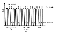
図1は、従来技術の4チャネルアレイ導波路ルータ(AWR)のブロック図である。このようなAWRは、米国特許第5,136,671号(発行日:1992年8月4日)に記載されている。図において、AWRは、入力導波路110、第1自由空間領域111、複数のチャープ導波路112、第2自由空間領域113、および複数の出力導波路102を有する。最初に、入力WDM信号は4つの波長1〜4を含むと仮定する。図示のように、AWRデバイス100は、デバイスの自由スペクトルレンジ(FSR)内に含まれるWDM入力信号101の4つの波長1〜4を、4つの異なる出力102へ分離する。通常、AWRは、FSR内に制限された波長範囲で用いられる。ここでは、AWRは、16個の波長を含むWDM信号を受信し、追加波長はFSRの外側にあると仮定する。この状況では、WDM信号は16個の波長を含むため、FSRの外側の追加波長もまた、波長ルータの「ラップアラウンド」性により、出力のうちの1つへルーティングされる。
【0008】
図2は、16個の波長の信号強度伝送レベルと、これらの波長が、図1のAWRの4つの出力チャネル102にどのように巡回的に分配される(すなわち、どのようにラップアラウンドする)かを示すグラフである。図示のように、FSRの4倍の波長レンジにわたる16個の波長チャネルを含む広いスペクトルのWDM入力信号に対して、4個の出力ポートはそれぞれ(約)1FSRだけ離れた4個の波長を出力することになる。すなわち、図2に示すように、出力ポート1は、波長1、5、9、および13を含み、出力ポート2は、波長2、6、10、および14を含み、などとなる。一般的には、M個(M>1)の波長チャネルを有する入力波長分割多重(WDM)信号を受信すると、N個(1<N<M)の出力の1次元アレイで、各出力n(1≦n≦N)は、WDM信号のチャネルn,n+N,n+2N,...,n+[M/N−1]Nを含むことになる。
【0009】
図1のAWRの各出力ポートの4個の重ね合わされた波長は、もちろん、各ポートごとに別のAWRを用いて個々の波長にさらに分離することができる。このような構成は、"Composite optical router with hierarchical routing levels and increased port capacity"という発明の名称の米国特許出願(出願日:1997年4月2日、発明者:M. Nuss, J. Start, and J. A. Walker)に記載されている。本発明の発明者の認識したところでは、AWRのこの部分的分離化特性を自由空間光ルータと組み合わせることにより、入力WDM信号を完全に分離化することができる。本発明による新規な2段光ルータは、有効に処理されるチャネル数を5倍以上に増大させるように、導波光学系段を自由空間段と組み合わせる。
【0010】
図3に示すように、本発明の一実施例は、AWRのすべての部分分離化出力ポート信号を、平面回折格子(グレーティング)を通して最終分離化出力面に投影することによって自由空間光波長を分離化し、完全に分離化された波長の2次元(2D)アレイスポットを生成する。図示のように、16波長WDM入力信号はAWR100(図1)の入力で受信され、4個の出力102からの部分分離化1次元信号アレイ102はレンズ301でコリメートされる。コリメートされた1次元信号アレイ102は、透過型平面回折格子(グレーティング)302に送られる。グレーティング302は、1次元信号アレイ102のそれぞれの部分分離化信号を個々の波長に分離化する。その結果、分離化された波長信号λ1〜λ16の2次元アレイが得られ、これらの波長はレンズ303により出力ファイバアレイ304へ集光される。波長信号λ1〜λ16の2次元アレイの集光された光スポット間隔(レイアウトパターン)は平面305に示される。
【0011】
スポットレイアウトパターン305は、グレーティング302の向きおよび空間周波数に依存する。図3に示すように、グレーティング302は、グレーティングを用いたラスタ走査波長スポットの長方形アレイを形成する。ここで、グレーティングラインは、部分分離化波長出力の行にほぼ平行である。
【0012】
図示のように、分離された波長λ1〜λ16は、波長分離化焦点面305に位置する2次元ファイバアレイ304の個々のファイバに送られ、各波長が出力ファイバのうちの1つに結合するようにされる。2次元ファイバアレイ304は、シングルモードファイバ結合に必要な精度で製造し位置合わせ(アラインメント)するのは困難であるが、このようなアレイは、例えば、面内にV溝アラインメント構造を有するシリコン基板のスタックとして組み立てたファイバを用いて製造することができる。このような2Dアレイは、文献において周知であり、シングルモードおよびマルチモードファイバ用のアレイコネクタを製造するために使用されている(例えば、A. R. Mickelson, N. R. Basavanhally, and Y. C. Lee, "Optoelectronic Packaging", John Wiley & Sons, 1997, Chapter 9, Section 4、を参照)。アラインメントの都合、小型化、単純化および頑強性のために、図3に示す透過型グレーティング302よりもむしろ反射型回折格子を使用するのが好ましい場合もある。
【0013】
図4に、図3のグレーティング302によって行われるのとほぼ同一の分離化機能を実行する反射型グレーティング401を用いた、本発明による導波/自由空間波長ルータの組合せのもう1つの実施例を示す。この構成では、レンズ301は、部分分離化信号アレイ102と、グレーティング401から反射された分離化信号アレイ402の両方のために使用される。この構成では、単一のレンズ301が、信号の1次元アレイ102をコリメートしてグレーティング401へ送り、そこで信号は反射され回折される。反射され回折された2次元の信号は、レンズ301により集光されて、分離化された信号アレイ402を形成し、これがファイバアレイ304に送られる。
【0014】
図5に示すもう1つの実施例では、部分的に分離化された複数の波長信号102は、グレーティング501を用いることにより1次元アレイへ送られる。グレーティング501の向きは、部分分離化導波路出力102の行にほぼ直交する。図示のように、部分分離化信号アレイ102は、レンズ301によってコリメートされ、反射型グレーティング501に送られる。反射型グレーティング501の直交する向きにより、部分分離化導波路出力102のそれぞれの波長は、部分分離化信号アレイ102に平行な1次元アレイ(502〜505)に分離化される。1次元アレイ502〜505の平行アラインメントにより、AWR100を有する導波路基板510は、分離化出力のための導波路511としても使用することができる。この構成により、2Dファイバアレイを使わずに済む。1次元出力ファイバアレイ512は、従来のAWRで用いられるのと同じシリコンオプティカルベンチのアラインメント技術を用いてAWRに接続される。なお、図5に示した導波路レイアウトは例示であり、チャネル間クロストーク、曲げおよび交差損失のような多くの考慮点が、実際のレイアウトで用いられる導波路形状を規定することになる。
【0015】
なお、さらに好ましい実施例では、1次元出力ファイバアレイ512を、レンズ301からの1次元スポットアレイ513に直接に結合することにより、2度目に導波路基板510に結合することによる追加損失が避けられる。これは、単に、導波路基板510の下に1次元出力ファイバアレイ512を配置することによって実現される。このような構成では、水平導波路511は不要であり、出力ファイバアレイ512は、部分分離化導波路出力102の真下にくることになる。
【0016】
多波長合分波スイッチのようなアプリケーションでは、多波長信号を分離化し、各波長を独立に操作した後、再び多重化する必要がある。空間光学系に基づき、微小機械傾斜ミラーを用いた1つの従来技術の光波長合分波スイッチ(OADM)が、"Reconfigurable Wavelength Division Multiplex Add/Drop Using Micromirrors"という発明の名称の米国特許出願(出願日:1997年11月12日、発明者:V. A. Aksyuk et al.)に記載されている。図6に、本発明による、導波/自由空間波長ルータと、微小機械傾斜ミラースイッチの2次元アレイの組合せを用いた実現されるWDM合分波スイッチの例を示す。
【0017】
図6に示すように、サーキュレータ601は、入力(IN)ポートにおいて受信WDM信号をAWR1に結合する。AWR1およびAWR2は、AWR100と同じように実現され動作する。なお、明確化のため、図6には、AWR1からの4個の部分分離化出力605のうちの1つのみからの波長を示す。AWR1からの部分分離化出力605は、レンズ606によりコリメートされて透過型平面回折格子(グレーティング)607に送られ、グレーティング607は1次元信号アレイ607aを生成する。レンズ608は、この1次元信号アレイを集光し、微小機械傾斜ミラースイッチ610の2次元(2D)アレイの対応する列609に送る。AWR1からの他の部分分離化出力605a〜605c(図示せず)もまた、レンズ606によりコリメートされて透過型平面回折格子607に送られ、グレーティング607は、AWR1からの部分分離化出力605a〜605cのそれぞれに対して1次元信号アレイ607aを生成する。こうして、グレーティング607は、分離化波長信号の2次元アレイを形成し、これはレンズ608によって、微小機械傾斜ミラースイッチ610の2次元(2D)アレイのそれぞれの列609、609a〜609cに集光される。微小機械傾斜ミラースイッチ610は、前掲のV. A. Aksyuk et al.の文献に記載されているように実現することが可能である。それぞれの傾斜ミラー素子は、同じパス(例えば607a)に沿って入射波長を反射するように独立に制御され、または、異なるパス611aへ波長を偏向させるように傾斜される。傾斜ミラー素子は、電気信号(図示せず)を用いて独立に制御される。
【0018】
ミラー素子609−2が、そのミラー素子に送られる電気信号(図示せず)によって制御されて第1角だけ傾斜していると仮定すると、パス608−2上の波長信号は、パス608−2に沿って反射され、レンズ608、グレーティング607、レンズ606を通り、パス605を通じてAWR1に戻り、サーキュレータ601に出力され、そこで、PASS(通過)ポートを出る。これは、図6のOADMを通って「通過」する波長がたどるパスを示す。これに対して、ミラー素子609−2が動作(傾斜)していない場合、パス608−2上の波長信号はレンズ611へ反射される。レンズ611は、ミラーアレイ610の非動作ミラー素子から反射されたすべての信号をグレーティング612に集光(611a)し、グレーティング612は、これらの波長を合成して合成信号612aをレンズ613に送る。レンズ613は、信号614をAWR2のポート615に集光する。AWR2の出力は、サーキュレータ602に出力され、そこで、DROP(分波)ポートを出る。これは、図6のOADMによって「分波」される波長がたどるパスを示す。
【0019】
なお、AWR1からの他の部分分離化出力605a〜605cのすべての「分波」される波長は、微小機械傾斜ミラースイッチの2次元(2D)アレイ610のそれぞれの列609、609a〜609cから反射され、同じくレンズ611によって透過型平面回折格子612に集光され、グレーティング612は、1次元信号アレイ612aを生成する。次に、レンズ613は、これらの信号をそれぞれAWR2の対応するポートに集光し、AWR2は、それらの信号を1つの合成信号に合成し、この合成信号はサーキュレータ602に結合され、そこで、DROPポートを出る。
【0020】
「合波」(ADD)される波長は、サーキュレータ602のADDポートに入り、AWR2を通じてレンズ613に結合され、グレーティング612、レンズ611を通り、アレイ610内のその波長に対応するミラー素子に至る。「合波」波長に対応するミラー素子は動作(検車)しており、「合波」波長を、「通過」パスに沿って反射し、この波長は、レンズ608、グレーティング607、レンズ606、AWR2、サーキュレータ601を通り、サーキュレータ601のINポートからの「通過」波長とともに、サーキュレータ601のPASSポートを出る。
【0021】
図6に示すように、個々のアプリケーションに応じて、2Dミラー素子アレイ610を用いて個々の波長信号を処理することにより、光を図3の2Dファイバアレイ304に結合すること(これは実現するのが困難あるいは高価である)が不要になる。さらに、2Dミラーデバイスアレイ610は、損失のある反射器(リフレクタ)として構成することが可能であり、これにより、米国特許第5,745,271号に記載されているデバイスと同様に機能するように、個々の波長信号の強度を減衰させるために使用することができる。プレーナ製造技術のため、ミラーデバイスの2Dアレイ610の設計および製造は、ファイバの2Dアレイに接続するよりもずっと容易に実現される。
【0022】
プレーナ製造技術の使用は、AWR(アレイ導波路ルータ)への入力スペクトルがFSR(自由スペクトルレンジ)を超え、AWRからの各出力がほぼFSRだけ離れた複数の信号を伝送することができる場合に特に有用である。プレーナ製造技術は、出力チャネルのピッチ(図2の202を参照)が出力チャネルの各「ラップアラウンド」ごとにわずかに変化するときに必要な正確なチャネル間隔に整合する能力を提供する。
【0023】
図6のWDM合分波スイッチ(OADM)は、前掲の従来技術の空間光学系に基づくOADMに比べて次の点で改善されている。
(1)処理可能なチャネル数が増大する(チャネルの2Dアレイのため)。
(2)各チャネルの素子性能が大幅に改善される。
この第2の利点が得られるのは、空間光学系に基づくOADMでは、デバイスの列が、通信チャネルどうしの間の間隔を0またはほぼ0とした連続波長信号によって照射されるためである。これに対して、図6のOADMでは、デバイスの各列は、少なくとも1つの完全なチャネル幅の「デッドスペース」だけ分離された別々の信号によって照射される。図2に示したように、このデッドスペースは、強度ピーク間の領域201である。強度ピークどうしの間のこのデッドスペースにより、機能の分離が可能となる。例えば、図7では、光信号701が、傾斜ミラースイッチユニット610のミラー素子702に入射している。図示のように、波長701と706の間のデッドスペース705を増大させることにより、ミラー素子702および703を大きくすることが可能となり、これにより、光強度ピーク(すなわち、光スポット704)がミラー素子702の中央領域に入り、ミラーの辺縁に触れないことになる可能性が高くなる。これが重要であるのは、好ましくない損失、散乱およびスイッチングクロストークはほとんどすべて、光スポット704がミラー素子702の辺縁で散乱されることにより生じるからである。また、デッドスペース705の増大により、パッキング密度が低減し、ミラー素子702の傾斜回路のための余裕が増大する。また、デッドスペース705の増大により、スポット704とミラー素子702の中心の間に要求されるアラインメント誤差が緩やかになる。
【0024】
図1において、導波路出力チャネル102は、好ましくない非一様なグリッド上で許容される伝送通過帯域(これにより光が比較的小さい損失で透過する)を規定する。しかし、図8に示すように、ABで示されるラインでAWRを終端することによって、出力をチャネル化することなく導波路から出ることも可能である。図8のラインABは、AWRの自由空間領域801の端部を単に劈開、エッチング、または研磨することにより形成することができる。
【0025】
導波路をABで終端した場合、出力は、連続広帯域光源(波長範囲はFSRのN倍)から自由空間に放射される。その結果、図9の901に示すように、N個の重ね合わされたスペクトルセグメントのセットが得られる。図6および図9をあわせて参照すると、このスペクトルは、図6の平面回折格子(例えば607)を通って分配されると、重ね合わされたセグメントは、それらをさらにチャネル化することなく分離される(902)。グレーティング607を照射するスペクトルパワー分布は、N個の連続スペクトルセグメントのセットとなる。図9に示すグレーティングの向きは、厳密に直交するグレーティングに対するスペクトル分布の、より正確な表現である。実際には、グレーティングは、照射スポットと整列するように数度だけ回転することができる。ユニット(あるいはアレイ)610のミラー素子は、個々のミラー素子(あるいはデバイス)がそれぞれ適当な空間位置に配置されるように配列される。
【0026】
一般に、図8の劈開アレイ導波路ルータの波長分散特性を、図6で用いられるAWR1およびAWR2の代わりに使用することが可能である。このような構成では、部分分離化信号は、切頭ルータAWR1を出て、自由空間光素子606、607および608を用いて(前述のように)処理され、ミラーアレイ610で反射された後、自由空間光素子606、607および608を通る2回目のパスで再結合されるか、第2の切頭ルータAWR2で多重化される。
【0027】
【発明の効果】
以上述べたごとく、本発明によれば、WDM伝送システムで使用されるチャネル数を5倍以上増大させるように自由空間と導波光学系を組み合わせたルータが実現される。
【図面の簡単な説明】
【図1】従来技術の4チャネルアレイ導波路ルータ(AWR)のブロック図である。
【図2】図1のAWRを通る信号強度伝送のグラフの図である。
【図3】本発明による、導波/自由空間波長ルータと2次元出力アレイの組合せの図である。
【図4】本発明による、導波/自由空間波長ルータと2次元出力アレイの組合せのもう1つの実施例の図である。
【図5】本発明による、導波/自由空間波長ルータと1次元出力アレイの組合せの実施例の図である。
【図6】本発明による、導波/自由空間波長ルータと、微小機械傾斜ミラースイッチの2次元アレイの組合せを用いて実現される光合分波マルチプレクサ(OADM:optical add/drop multiplexer)の図である。
【図7】ミラー素子に入射する光信号の図である。
【図8】AWRの変形例の図である。
【図9】図8の変形AWRからの分散出力の図である。
【符号の説明】
100 AWRデバイス
101 WDM入力信号
102 出力導波路
110 入力導波路
111 第1自由空間領域
112 チャープ導波路
113 第2自由空間領域
301 レンズ
302 透過型平面回折格子(グレーティング)
303 レンズ
304 出力ファイバアレイ
305 波長分離化焦点面
401 反射型グレーティング
402 分離化された信号アレイ
501 反射型グレーティング
502〜505 1次元アレイ
510 導波路基板
511 導波路
512 1次元出力ファイバアレイ
601 サーキュレータ
602 サーキュレータ
605 部分分離化出力
606 レンズ
607 透過型平面回折格子
607a 1次元信号アレイ
608 レンズ
610 微小機械傾斜ミラースイッチ
611 レンズ
612 透過型平面回折格子(グレーティング)
612a 合成信号
613 レンズ
701 光信号
702 ミラー素子
703 ミラー素子
704 光スポット
705 デッドスペース
801 自由空間領域[0001]
BACKGROUND OF THE INVENTION
The present invention relates to a multi-wave optical router used in a wavelength division multiplexing (WDM) system, and more particularly to a router combining free space and waveguide optics to increase the number of wavelength channels that can be processed by such a router. About.
[0002]
[Prior art]
Wavelength division multiplexing (WDM) transmission systems currently use integrated optical array waveguide routers (AWRs) to multiplex multiple wavelength signals onto a single fiber and receive signals through the fiber. Is separated. However, as the number of channels used in a WDM transmission system increases, it becomes increasingly difficult to design and manufacture a suitable AWR. Difficult points in that case include forming a flat pass band and suppressing cross-channel crosstalk from many output lines. Using today's technology, it would be possible to produce a 128 channel router at 50 GHz intervals, but a new approach would probably be needed to further increase the number of channels.
[0003]
[Problems to be solved by the invention]
There is a need for a technique that increases the number of channels that can be used in a WDM transmission system.
[0004]
[Means for Solving the Problems]
According to the method and apparatus of the present invention, a router combining free space and a waveguide optical system is realized so as to increase the number of channels used in a WDM transmission system by five times or more. The inventor of the present invention has recognized that the input WDM signal can be completely separated by combining the partial separation characteristics of the arrayed waveguide router (AWR) with the free space optical router. Using this two-stage router, an output wavelength signal can be obtained in both one-dimensional and two-dimensional arrays.
[0005]
Specifically, according to the present invention, an optical device includes an optical array waveguide router (AWR) that receives an input wavelength division multiplexing (WDM) signal having M (M> 1) wavelength channels, and an AWR. And a one-dimensional array of N outputs (1 <N <M) that output WDM signals. Each output n (1 ≦ n ≦ N) includes a partially separated signal having a plurality of wavelength channels n, n + N, n + 2N,..., N + [M / N−1] N of the WDM signal. . A free space optical wavelength channel demultiplexer receives each partially separated signal and then generates M wavelength channels. Each of these M wavelength channels is output from a different output of the M outputs.
[0006]
According to another aspect of the invention, a free space optical wavelength channel demultiplexer is implemented using a combination of one or more lenses and a transmissive or reflective grating. According to another feature of the invention, the M outputs can be terminated with a one-dimensional array of fibers or a two-dimensional array of fibers or mirror elements. According to another feature, each mirror element of the mirror element array is independently controlled and multiplexed wavelength to reflect the associated wavelength and pass the device back to the original AWR or the second AWR. Controls such as signal switching.
[0007]
DETAILED DESCRIPTION OF THE INVENTION
FIG. 1 is a block diagram of a prior art 4-channel array waveguide router (AWR). Such an AWR is described in US Pat. No. 5,136,671 (issue date: August 4, 1992). In the figure, the AWR has an
[0008]
FIG. 2 shows signal strength transmission levels of 16 wavelengths and how these wavelengths are cyclically distributed (ie how wrap around) to the four
[0009]
The four superimposed wavelengths of each output port of the AWR of FIG. 1 can of course be further separated into individual wavelengths using a separate AWR for each port. Such a configuration is based on the US patent application entitled “Composite optical router with hierarchical routing levels and increased port capacity” (Filing date: April 2, 1997, Inventor: M. Nuss, J. Start, and JA Walker). The inventors of the present invention have recognized that the input WDM signal can be completely separated by combining this partial separation characteristic of the AWR with a free space optical router. The novel two-stage optical router according to the present invention combines a waveguide optics stage with a free space stage so as to increase the number of effectively processed channels by more than five times.
[0010]
As shown in FIG. 3, one embodiment of the present invention separates free-space light wavelengths by projecting all partially separated output port signals of the AWR onto a final separated output surface through a planar grating (grating). To produce a two-dimensional (2D) array spot of fully separated wavelengths. As shown, a 16 wavelength WDM input signal is received at the input of the AWR 100 (FIG. 1), and the partially separated one-
[0011]
The
[0012]
As shown, the separated wavelengths λ 1 -λ 16 are sent to individual fibers of a two-
[0013]
FIG. 4 illustrates another embodiment of a waveguide / free space wavelength router combination according to the present invention using a reflective grating 401 that performs substantially the same separation function as performed by the grating 302 of FIG. Show. In this configuration, the
[0014]
In another embodiment shown in FIG. 5, a plurality of partially separated wavelength signals 102 are sent to a one-dimensional array by using a grating 501. The orientation of the grating 501 is substantially orthogonal to the row of partially separated waveguide outputs 102. As illustrated, the partially separated
[0015]
In a further preferred embodiment, the 1-dimensional
[0016]
In applications such as multi-wavelength multiplexing / demultiplexing switches, it is necessary to demultiplex multi-wavelength signals, operate each wavelength independently, and then multiplex again. One prior art optical wavelength multiplexing / demultiplexing switch (OADM) based on spatial optics and using micromechanical tilting mirrors is a US patent application entitled “Reconfigurable Wavelength Division Multiplex Add / Drop Using Micromirrors”. Date: November 12, 1997, inventor: VA Aksyuk et al.). FIG. 6 shows an example of a WDM multiplexing / demultiplexing switch realized using a combination of a waveguide / free space wavelength router and a two-dimensional array of micro mechanical tilt mirror switches according to the present invention.
[0017]
As shown in FIG. 6,
[0018]
Assuming that mirror element 609-2 is tilted by a first angle controlled by an electrical signal (not shown) sent to that mirror element, the wavelength signal on path 608-2 is the path 608-2. , Passes through
[0019]
Note that all “demultiplexed” wavelengths of the other partially separated
[0020]
A wavelength that is “multiplexed” (ADD) enters the ADD port of
[0021]
As shown in FIG. 6, depending on the particular application, the light is coupled to the
[0022]
The use of planar manufacturing technology is when the input spectrum to the AWR (arrayed waveguide router) exceeds FSR (free spectral range) and each output from the AWR can carry multiple signals separated by approximately FSR. It is particularly useful. Planar manufacturing techniques provide the ability to match the exact channel spacing required when the output channel pitch (see 202 in FIG. 2) varies slightly for each “wraparound” of the output channel.
[0023]
The WDM multiplexing / demultiplexing switch (OADM) shown in FIG. 6 is improved in the following points as compared with the OADM based on the above-described prior art spatial optical system.
(1) The number of channels that can be processed increases (due to a 2D array of channels).
(2) The device performance of each channel is greatly improved.
This second advantage is obtained because in OADMs based on spatial optics, a column of devices is illuminated by a continuous wavelength signal with zero or nearly zero spacing between communication channels. In contrast, in the OADM of FIG. 6, each column of devices is illuminated by a separate signal separated by a “dead space” of at least one full channel width. As shown in FIG. 2, this dead space is a
[0024]
In FIG. 1, the
[0025]
When the waveguide is terminated with AB, the output is emitted into free space from a continuous broadband light source (wavelength range N times FSR). The result is a set of N superimposed spectral segments, as shown at 901 in FIG. Referring to FIGS. 6 and 9 together, when this spectrum is distributed through the planar diffraction grating (eg, 607) of FIG. 6, the superimposed segments are separated without further channeling them. (902). The spectral power distribution that illuminates the grating 607 is a set of N consecutive spectral segments. The grating orientation shown in FIG. 9 is a more accurate representation of the spectral distribution for a strictly orthogonal grating. In practice, the grating can be rotated by a few degrees to align with the illumination spot. The mirror elements of the unit (or array) 610 are arranged so that the individual mirror elements (or devices) are arranged at appropriate spatial positions.
[0026]
In general, the chromatic dispersion characteristics of the cleaved array waveguide router of FIG. 8 can be used in place of AWR1 and AWR2 used in FIG. In such a configuration, the partially separated signal exits the truncated router AWR1, is processed using free space
[0027]
【The invention's effect】
As described above, according to the present invention, a router in which free space and a waveguide optical system are combined so as to increase the number of channels used in a WDM transmission system by five times or more is realized.
[Brief description of the drawings]
FIG. 1 is a block diagram of a prior art 4-channel array waveguide router (AWR).
2 is a graph of signal strength transmission through the AWR of FIG.
FIG. 3 is a diagram of a combination waveguide / free space wavelength router and two-dimensional output array in accordance with the present invention.
FIG. 4 is a diagram of another embodiment of a combination waveguide / free space wavelength router and two-dimensional output array in accordance with the present invention.
FIG. 5 is a diagram of an embodiment of a combination waveguide / free space wavelength router and one-dimensional output array in accordance with the present invention.
FIG. 6 is a diagram of an optical add / drop multiplexer (OADM) implemented using a two-dimensional array of waveguide / free space wavelength routers and micromechanical tilt mirror switches according to the present invention. is there.
FIG. 7 is a diagram of an optical signal incident on a mirror element.
FIG. 8 is a diagram of a modified example of AWR.
FIG. 9 is a diagram of distributed output from the modified AWR of FIG.
[Explanation of symbols]
100
303
612a Composite signal 613
Claims (14)
コリメートするレンズとグレーティングとを含んでなる自由空間光波長チャネルデマルチプレクサであって、部分分離化信号チャネルのN個の自由空間光信号の各々を受信して、M個の波長チャネルを生成する自由空間光波長チャネルデマルチプレクサを備え、M個の波長チャネルの各々がM個の出力のうちの相異なる出力から出力されることを特徴とする光装置。N (1 <N <M) outputs that receive input wavelength division multiplexed (hereinafter “WDM”) signals having M (M> 1) wavelength channels and output WDM signals within the free spectral range Each of the outputs n (1 ≦ n ≦ N) for outputting an optical signal to a free space is a plurality of WDM signals, each having one optical array waveguide router (hereinafter “AWR”) having one one-dimensional array of A partially demultiplexed signal having wavelength channels n, n + N, n + 2N,..., N + [M / N−1] N,
A free-space optical wavelength channel demultiplexer comprising a collimating lens and a grating , receiving each of the N free-space optical signals of the partially separated signal channel and generating M wavelength channels An optical device comprising a spatial light wavelength channel demultiplexer, wherein each of M wavelength channels is output from a different output of M outputs.
N個の出力の1次元アレイからの部分分離化信号チャネルをグレーティング上へコリメートする第1レンズを含み、
前記グレーティングは、部分分離化信号の1次元アレイをそれぞれ個々の波長チャネルに分離化して波長チャネルの2次元アレイを形成する透過型グレーティングであり、さらに、
波長チャネルの2次元アレイを素子の2次元アレイに集光する第2レンズを含むことを特徴とする請求項1に記載の装置。The free space optical wavelength channel demultiplexer comprises:
A first lens that collimates a partially separated signal channel from a one-dimensional array of N outputs onto the grating;
The grating is a transmissive grating that separates a one-dimensional array of partially separated signals into individual wavelength channels to form a two-dimensional array of wavelength channels;
The apparatus of claim 1 including a second lens that focuses the two-dimensional array of wavelength channels onto the two-dimensional array of elements.
該第2グレーティングは、同じ部分分離化信号からの反射された波長チャネルの各々を1つの合成信号に多重化する透過型グレーティングであり、そして
該合成信号は、第4レンズにより、第2AWRに集光されることを特徴とする請求項5に記載の装置。When the second control signal is sent to the mirror element, the mirror element reflects the wavelength channel, and the reflected wavelength channel is condensed on the second grating by the third lens;
The second grating is a transmissive grating that multiplexes each of the reflected wavelength channels from the same partially separated signal into one composite signal, and the composite signal is collected by the fourth lens at the second AWR. 6. The device of claim 5, wherein the device is illuminated.
前記第2AWRとの間で信号を結合する第2サーキュレータとをさらに有することを特徴とする請求項6に記載の装置。A first circulator for coupling a signal to and from the AWR;
The apparatus according to claim 6, further comprising a second circulator that couples a signal to and from the second AWR.
WDM信号を受信する入力導波路と、
前記入力導波路と、チャープ導波路のセットの第1端との両方に接続された第1自由空間領域と、
前記チャープ導波路のセットの第2端と、N個の出力の1次元アレイで終端するN個の出力導波路のセットとの両方に接続された第2自由空間領域とを有することを特徴とする請求項8に記載の装置。The AWR and the second AWR are respectively
An input waveguide for receiving a WDM signal;
A first free space region connected to both the input waveguide and a first end of a set of chirped waveguides;
A second free space region connected to both a second end of the set of chirped waveguides and a set of N output waveguides terminating in a one-dimensional array of N outputs. The apparatus according to claim 8.
N個の出力の1次元アレイからの部分分離化信号チャネルをグレーティング上に集光する第1レンズを有し、
前記グレーティングは、部分分離化信号の1次元アレイをそれぞれ個々の波長チャネルに分離化して波長チャネルの1次元アレイを形成する反射型グレーティングであり、さらに、
前記第1レンズは、波長チャネルの1次元アレイを素子の1次元アレイに集光することを特徴とする請求項1に記載の装置。The free space optical wavelength channel demultiplexer comprises:
A first lens for concentrating partially separated signal channels from a one-dimensional array of N outputs onto the grating;
The grating is a reflective grating that forms a one-dimensional array of wavelength channels by separating the one-dimensional array of partially separated signals into individual wavelength channels, respectively.
The apparatus of claim 1, wherein the first lens focuses a one-dimensional array of wavelength channels onto a one-dimensional array of elements.
コリメートするレンズとグレーティングとを含んでなる自由空間光波長チャネルデマルチプレクサであって、AWR出力からの自由空間光信号を受信して、M個の波長チャネルを生成する自由空間光波長チャネルデマルチプレクサとを備え、
前記自由空間光波長チャネルデマルチプレクサは、AWRとは異なる平面に方向付けられ、M個の波長チャネルの各々がM個の出力のうちの相異なる出力から出力されることを特徴とする光装置。One planar optical array waveguide router (see below) having an output that receives an input wavelength division multiplexed (hereinafter “WDM”) signal having M (M> 1) wavelength channels and outputs the optical signal to free space ( Hereinafter referred to as “AWR”),
A free space optical wavelength channel demultiplexer comprising a collimating lens and a grating, the free space optical wavelength channel demultiplexer receiving a free space optical signal from an AWR output and generating M wavelength channels; With
The free space optical wavelength channel demultiplexer is directed to a plane different from the AWR, and each of the M wavelength channels is output from a different output of the M outputs.
WDM信号を受信する入力導波路と、
前記入力導波路と、チャープ導波路のセットの第1端との両方に接続された第1自由空間領域と、
前記チャープ導波路のセットの第2端に接続された第2自由空間領域の第1側と、
前記AWRの出力として作用する直線端部を形成する第2自由空間領域の第2側とを含むことを特徴とする請求項13に記載の装置。The AWR is
An input waveguide for receiving a WDM signal;
A first free space region connected to both the input waveguide and a first end of a set of chirped waveguides;
A first side of a second free space region connected to a second end of the set of chirped waveguides;
14. The apparatus of claim 13, including a second side of a second free space region forming a straight end that acts as an output of the AWR.
Applications Claiming Priority (2)
| Application Number | Priority Date | Filing Date | Title |
|---|---|---|---|
| US09/311544 | 1999-05-13 | ||
| US09/311,544 US6263127B1 (en) | 1999-05-13 | 1999-05-13 | Free-space/arrayed-waveguide router |
Publications (2)
| Publication Number | Publication Date |
|---|---|
| JP2000347065A JP2000347065A (en) | 2000-12-15 |
| JP4043693B2 true JP4043693B2 (en) | 2008-02-06 |
Family
ID=23207383
Family Applications (1)
| Application Number | Title | Priority Date | Filing Date |
|---|---|---|---|
| JP2000137227A Expired - Fee Related JP4043693B2 (en) | 1999-05-13 | 2000-05-10 | Optical device |
Country Status (5)
| Country | Link |
|---|---|
| US (1) | US6263127B1 (en) |
| EP (1) | EP1052868B1 (en) |
| JP (1) | JP4043693B2 (en) |
| AT (1) | ATE410847T1 (en) |
| DE (1) | DE60040431D1 (en) |
Families Citing this family (100)
| Publication number | Priority date | Publication date | Assignee | Title |
|---|---|---|---|---|
| DE19815404A1 (en) * | 1998-04-06 | 1999-10-14 | Siemens Ag | Arrangement for spatial separation and / or merging of optical wavelength channels |
| US7127172B1 (en) * | 1999-06-02 | 2006-10-24 | Massachusetts Institute Of Technology | Optical frequency filter |
| US6788849B1 (en) * | 1999-11-12 | 2004-09-07 | Cme Telemetrix Inc. | Volume or stacked holographic diffraction gratings for wavelength division multiplexing and spectroscopy |
| US6535311B1 (en) | 1999-12-09 | 2003-03-18 | Corning Incorporated | Wavelength selective cross-connect switch using a MEMS shutter array |
| CA2300780C (en) * | 2000-03-15 | 2007-08-07 | Nortel Networks Corporation | Integrated photonic switch |
| US6763163B1 (en) * | 2000-07-26 | 2004-07-13 | Lucent Technologies Inc. | Method and apparatus for spatial-shift wavelength multiplexing in communication systems |
| US6381387B1 (en) * | 2000-08-02 | 2002-04-30 | Networks Photonics, Inc. | Athermalization of a wavelength routing element |
| US6532318B1 (en) * | 2000-10-18 | 2003-03-11 | Corning Incorporated | Symmetric wavelength selective switch for interconnecting two WDM rings |
| DE10053498A1 (en) * | 2000-10-27 | 2002-05-16 | Zeiss Carl | Cross coupler for optical communications |
| WO2002043202A1 (en) * | 2000-11-27 | 2002-05-30 | Zhongshan Liu | Multi-group multi-wavelength laser matrix |
| CA2328696C (en) * | 2000-12-18 | 2008-08-12 | Jds Uniphase Inc. | Periodic arrayed waveguide grating multiplexer/demultiplexer |
| US6978062B2 (en) | 2001-02-21 | 2005-12-20 | Ibsen Photonics A/S | Wavelength division multiplexed device |
| WO2002071672A2 (en) * | 2001-03-01 | 2002-09-12 | Zolo Technologies, Inc. | (de)multiplexer with interleaver for producing a flat-top filter function and enhanced channel separation |
| US20020131683A1 (en) * | 2001-03-15 | 2002-09-19 | Doerr Christopher Richard | Planar lightwave wavelength blocker devices using micromachines |
| US6625346B2 (en) * | 2001-03-19 | 2003-09-23 | Capella Photonics, Inc. | Reconfigurable optical add-drop multiplexers with servo control and dynamic spectral power management capabilities |
| US6751372B2 (en) * | 2001-03-19 | 2004-06-15 | At&T Corp | Four-port wavelength-selective crossbar switches (4WCS) using reciprocal WDM MUX-DEMUX and optical circulator combination |
| WO2002075410A1 (en) * | 2001-03-19 | 2002-09-26 | Capella Photonics, Inc. | Reconfigurable optical add-drop multiplexers |
| US7019883B2 (en) * | 2001-04-03 | 2006-03-28 | Cidra Corporation | Dynamic optical filter having a spatial light modulator |
| WO2002082166A2 (en) * | 2001-04-03 | 2002-10-17 | Cidra Corporation | Variable optical source |
| US7126740B2 (en) * | 2001-04-03 | 2006-10-24 | Cidra Corporation | Multifunctional optical device having a spatial light modulator with an array of micromirrors |
| US20030090756A1 (en) * | 2001-09-25 | 2003-05-15 | Cidra Corporation | Optical channel monitor having an array of micro-mirrors |
| US6922277B2 (en) | 2001-09-25 | 2005-07-26 | Cidra Corporation | Optical interleaver/deinterleaver device having an array of micro-mirrors |
| US6956687B2 (en) * | 2001-04-03 | 2005-10-18 | Cidra Corporation | Optical blocking filter having an array of micro-mirrors |
| US20030095307A1 (en) * | 2001-09-25 | 2003-05-22 | Cidra Corporation | Reconfigurable optical add/drop multiplexer having an array of micro-mirrors |
| US6934069B2 (en) | 2001-04-03 | 2005-08-23 | Cidra Corporation | Chromatic dispersion compensation device having an array of micromirrors |
| GB2374457A (en) * | 2001-04-09 | 2002-10-16 | Bookham Technology Plc | Hybridised Fibre Amplifier/Waveguide Structures |
| US20020172454A1 (en) * | 2001-05-15 | 2002-11-21 | Chromux Technologies, Inc. | Reconfigurable optical add/drop module |
| US20020181876A1 (en) * | 2001-05-18 | 2002-12-05 | Chromux Technologies, Inc | Reconfigurable optical add/drop module |
| US7463828B2 (en) * | 2001-06-01 | 2008-12-09 | John Moon | Optical channel monitor |
| US7253897B2 (en) | 2001-06-01 | 2007-08-07 | Cidra Corporation | Optical spectrum analyzer |
| CA2351990A1 (en) * | 2001-06-26 | 2002-12-26 | Ibm Canada Limited-Ibm Canada Limitee | Rule based engine for validating financial transactions |
| US6625342B2 (en) * | 2001-07-03 | 2003-09-23 | Network Photonics, Inc. | Systems and methods for overcoming stiction using a lever |
| US6873447B2 (en) * | 2001-07-03 | 2005-03-29 | Pts Corporation | Two-dimensional free-space optical wavelength routing element based on stepwise controlled tilting mirrors |
| US6707959B2 (en) * | 2001-07-12 | 2004-03-16 | Jds Uniphase Inc. | Wavelength switch |
| JP2003029168A (en) * | 2001-07-17 | 2003-01-29 | Fujitsu Ltd | Variable wavelength dispersion compensator |
| CA2454631A1 (en) | 2001-07-20 | 2003-01-30 | Essex Corporation | Method and apparatus for optical signal processing using an optical tapped delay line |
| US6842239B2 (en) | 2001-08-10 | 2005-01-11 | Ibsen Photonics A/S | Alignment of multi-channel diffractive WDM device |
| US7298540B2 (en) * | 2001-08-22 | 2007-11-20 | Avanex Corporation | Equalizing optical wavelength routers |
| US7085492B2 (en) | 2001-08-27 | 2006-08-01 | Ibsen Photonics A/S | Wavelength division multiplexed device |
| US7164859B2 (en) * | 2001-08-29 | 2007-01-16 | Capella Photonics, Inc. | Free-space dynamic wavelength routing systems with interleaved channels for enhanced performance |
| GB0121308D0 (en) | 2001-09-03 | 2001-10-24 | Thomas Swan & Company Ltd | Optical processing |
| US7106920B2 (en) * | 2001-11-13 | 2006-09-12 | Zhongshan Liu | Laser array for generating stable multi-wavelength laser outputs |
| FR2832812B1 (en) * | 2001-11-29 | 2004-01-23 | Commissariat Energie Atomique | OPTICAL CHANNEL MATRIX MULTIPLEXING DEVICE, APPLICATION TO WAVELENGTH MULTIPLEXING AND INSERTION-EXTRACTION |
| US6658181B2 (en) | 2002-01-02 | 2003-12-02 | Wavesplitter Technologies, Inc. | Polarization interleaver |
| WO2003065097A2 (en) * | 2002-01-28 | 2003-08-07 | Cidra Corporation | Multifunctional optical device having a spatial light modulator with an array of micromirrors |
| US20040208584A1 (en) * | 2002-01-29 | 2004-10-21 | Keller Robert C. | Reconfigurable optical add-drop multiplexer using an analog mirror device |
| US7116910B1 (en) | 2002-04-10 | 2006-10-03 | Terabeam Corporation | Free space optical tap and multi/demultiplexer |
| JP4487089B2 (en) * | 2002-05-20 | 2010-06-23 | ジェーディーエス・ユニフェーズ・コーポレーション | Reconfigurable optical add / drop module, system and method |
| WO2003098962A2 (en) * | 2002-05-20 | 2003-11-27 | Metconnex Canada Inc. | Wavelength cross-connect |
| ATE341173T1 (en) * | 2002-05-20 | 2006-10-15 | Metconnex Canada Inc | WAVELENGTH SELECTIVE SWITCH |
| US20040018019A1 (en) * | 2002-07-26 | 2004-01-29 | Lacey Jonathan P. | Interleaver-based multiplexer and demultiplexer |
| WO2004015469A1 (en) * | 2002-08-08 | 2004-02-19 | The Regents Of The University Of California | Wavelength-selective 1xn2 switches with two-dimensional input/output fiber arrays |
| JP3852409B2 (en) * | 2003-02-04 | 2006-11-29 | 富士通株式会社 | Optical functional device |
| JP4031998B2 (en) * | 2003-02-20 | 2008-01-09 | 富士通株式会社 | Wavelength multiplexing processor |
| US7203398B2 (en) * | 2003-03-20 | 2007-04-10 | Texas Instruments Incorporated | Compact DMD-based optical module |
| US7181095B1 (en) * | 2003-07-29 | 2007-02-20 | Cisco Technology, Inc. | Low loss, noise filtering multiplexer/demultiplexer for reconfigurable OADMs |
| US20050078911A1 (en) * | 2003-10-14 | 2005-04-14 | Mikes Thomas L. | System and method for using a concentric spectrometer to multiplex or demultiplex optical signals |
| US7099528B2 (en) * | 2004-01-07 | 2006-08-29 | International Business Machines Corporation | Methods and devices for coupling electromagnetic radiation using diffractive optical elements |
| JP3721565B2 (en) * | 2004-02-27 | 2005-11-30 | 学校法人慶應義塾 | Optical functional waveguide, optical modulator, arrayed waveguide diffraction grating, and dispersion compensation circuit |
| JP4513471B2 (en) * | 2004-09-14 | 2010-07-28 | 沖電気工業株式会社 | Demultiplexer |
| JP4368286B2 (en) | 2004-10-08 | 2009-11-18 | 富士通株式会社 | Optical switch device |
| JP4568579B2 (en) * | 2004-10-29 | 2010-10-27 | 富士通株式会社 | Light switch |
| JP4445373B2 (en) * | 2004-10-29 | 2010-04-07 | 富士通株式会社 | Light switch |
| JP4530805B2 (en) * | 2004-11-02 | 2010-08-25 | 富士通株式会社 | Optical switch and optical transmission device |
| JP4382635B2 (en) * | 2004-11-10 | 2009-12-16 | 富士通株式会社 | Optical transmission equipment |
| JP4505313B2 (en) * | 2004-11-12 | 2010-07-21 | 富士通株式会社 | Optical device and optical control method |
| JP4476140B2 (en) * | 2005-03-07 | 2010-06-09 | 富士通株式会社 | Wavelength selective switch |
| JP4545023B2 (en) * | 2005-03-14 | 2010-09-15 | 富士通株式会社 | Chromatic dispersion and dispersion slope compensator |
| JP4500720B2 (en) * | 2005-03-29 | 2010-07-14 | 富士通株式会社 | Light switch |
| JP4493538B2 (en) * | 2005-03-31 | 2010-06-30 | 富士通株式会社 | Wavelength selective switch |
| US7362930B2 (en) * | 2005-04-11 | 2008-04-22 | Capella Photonics | Reduction of MEMS mirror edge diffraction in a wavelength selective switch using servo-based rotation about multiple non-orthogonal axes |
| US7352927B2 (en) | 2005-04-11 | 2008-04-01 | Capella Photonics | Optical add-drop multiplexer architecture with reduced effect of mirror edge diffraction |
| US7346234B2 (en) * | 2005-04-11 | 2008-03-18 | Capella Photonics | Reduction of MEMS mirror edge diffraction in a wavelength selective switch using servo-based multi-axes rotation |
| US7756368B2 (en) * | 2005-04-11 | 2010-07-13 | Capella Photonics, Inc. | Flex spectrum WSS |
| US7539371B2 (en) | 2005-04-11 | 2009-05-26 | Capella Photonics, Inc. | Optical apparatus with reduced effect of mirror edge diffraction |
| WO2007006142A1 (en) * | 2005-07-08 | 2007-01-18 | Jds Uniphase Corporation | Wavelength cross connect with per port performance characteristics |
| US7567756B2 (en) * | 2005-08-03 | 2009-07-28 | Capella Photonics | Method of automatic adjustment of dither amplitude of MEMS mirror arrays |
| DE102005051290A1 (en) * | 2005-10-26 | 2007-05-03 | Siemens Ag | Add-drop device for wavelength multiplexed signals |
| JP4908838B2 (en) * | 2005-12-13 | 2012-04-04 | 富士通株式会社 | Multi-wavelength spectrometer |
| AU2008205423B2 (en) * | 2007-08-13 | 2013-09-12 | Lumentum Operations Llc | Light steering using an array of tunable phase delay elements |
| US8175427B2 (en) * | 2007-09-18 | 2012-05-08 | Rockwell Automation Technologies, Inc. | Apparatus and methods for use of a tunable optical source in safety curtain applications |
| JP4960294B2 (en) * | 2008-04-17 | 2012-06-27 | 日本電信電話株式会社 | Wavelength selective switch |
| JP5015881B2 (en) * | 2008-09-02 | 2012-08-29 | 日本電信電話株式会社 | Variable dispersion compensator |
| JP5651904B2 (en) * | 2011-04-14 | 2015-01-14 | 独立行政法人産業技術総合研究所 | N × N wavelength selective switch |
| CA2871072C (en) | 2012-04-19 | 2020-07-14 | Zolo Technologies, Inc. | In-furnace retro-reflectors with steerable tunable diode laser absorption spectrometer |
| US8867920B2 (en) | 2012-07-24 | 2014-10-21 | International Business Machines Corporation | Optical de-multiplexing device |
| GB2504970A (en) | 2012-08-15 | 2014-02-19 | Swan Thomas & Co Ltd | Optical device and methods to reduce cross-talk |
| CN103197388B (en) * | 2013-04-19 | 2015-09-16 | 武汉邮电科学研究院 | C+L band wavelength selector switch and its implementation and processing unit |
| US9025958B1 (en) | 2013-09-03 | 2015-05-05 | Avago Technologies General Ip (Singapore) Pte. Ltd. | Planar lightwave circuit optical multiplexer for non-sequential wavelength channels |
| AU2016333145B2 (en) | 2015-09-28 | 2020-04-02 | Baraja Pty Ltd | Spatial profiling system and method |
| CA3044075A1 (en) | 2016-11-16 | 2018-05-24 | Baraja Pty Ltd | An optical beam director |
| CA3046812A1 (en) | 2016-12-16 | 2018-06-21 | Baraja Pty Ltd | Estimation of spatial profile of environment |
| US10578807B2 (en) | 2017-02-28 | 2020-03-03 | Nokia Of America Corporation | Optical apparatus with paired input and output planar waveguides coupled to a reflective modulator |
| CA3073095A1 (en) | 2017-08-25 | 2019-02-28 | Baraja Pty Ltd | Estimation of spatial profile of environment |
| CA3074245A1 (en) * | 2017-09-06 | 2019-03-14 | Baraja Pty Ltd | An optical beam director |
| EP3756287A1 (en) * | 2018-02-22 | 2020-12-30 | 8 Rivers Capital, LLC | System for multi-channel, diverged-beam optical wireless communication |
| JP7372783B2 (en) | 2019-08-26 | 2023-11-01 | 株式会社Subaru | Free space optical communication receiver |
| CN113448022B (en) * | 2020-03-24 | 2022-04-22 | 华为技术有限公司 | Optical transmitter, optical module, optical transceiver, and optical communication system |
| GB2595863A (en) * | 2020-06-08 | 2021-12-15 | Rushmere Tech Limited | Optical apparatus and associated methods |
| WO2021250393A1 (en) | 2020-06-08 | 2021-12-16 | Rushmere Technology Limited | Optical apparatus for and methods of generating optical signals to increase the amount of data in an optical network |
Family Cites Families (5)
| Publication number | Priority date | Publication date | Assignee | Title |
|---|---|---|---|---|
| US5701371A (en) * | 1994-10-31 | 1997-12-23 | Nippon Telegraph And Telephone Corporation | Tunable optical filter |
| US5726786A (en) * | 1995-11-21 | 1998-03-10 | The Aerospace Corporation | Free-space star-coupled optical data bus |
| GB2316759A (en) * | 1996-07-30 | 1998-03-04 | Northern Telecom Ltd | Optical multiplexer/demultiplexer having diffraction gratings in tandem |
| US5889906A (en) * | 1997-05-28 | 1999-03-30 | Lucent Technologies Inc. | Signal router with coupling of multiple waveguide modes for provicing a shaped multi-channel radiation pattern |
| US6049640A (en) * | 1997-09-04 | 2000-04-11 | Lucent Technologies Inc. | Wavelength-division-multiplexing cross-connect using angular dispersive elements and phase shifters |
-
1999
- 1999-05-13 US US09/311,544 patent/US6263127B1/en not_active Expired - Lifetime
-
2000
- 2000-05-03 DE DE60040431T patent/DE60040431D1/en not_active Expired - Fee Related
- 2000-05-03 AT AT00303681T patent/ATE410847T1/en not_active IP Right Cessation
- 2000-05-03 EP EP00303681A patent/EP1052868B1/en not_active Expired - Lifetime
- 2000-05-10 JP JP2000137227A patent/JP4043693B2/en not_active Expired - Fee Related
Also Published As
| Publication number | Publication date |
|---|---|
| EP1052868A3 (en) | 2004-04-07 |
| EP1052868B1 (en) | 2008-10-08 |
| ATE410847T1 (en) | 2008-10-15 |
| JP2000347065A (en) | 2000-12-15 |
| US6263127B1 (en) | 2001-07-17 |
| DE60040431D1 (en) | 2008-11-20 |
| EP1052868A2 (en) | 2000-11-15 |
Similar Documents
| Publication | Publication Date | Title |
|---|---|---|
| JP4043693B2 (en) | Optical device | |
| JP3852409B2 (en) | Optical functional device | |
| US7236660B2 (en) | Reconfigurable optical add-drop module, system and method | |
| US7509048B2 (en) | Method and apparatus for optical signal processing using an optical tapped delay line | |
| US7321704B2 (en) | Wavelength cross connect with per port performance characteristics | |
| JP4254776B2 (en) | Optical functional device | |
| US20070041683A1 (en) | Tunable Optical Filter | |
| US6959129B2 (en) | Bidirectional multiplexer and demultiplexer based on a single echelle waveguide grating | |
| US7529441B2 (en) | Wavelength routing optical switch | |
| EP1506689B1 (en) | Wavelength selective switch | |
| US7079728B2 (en) | Wavelength multiplexing processing apparatus | |
| US6496616B2 (en) | Miniature monolithic optical demultiplexer | |
| US20030063385A1 (en) | Optical multiplexer/demultiplexer and adjustment method thereof | |
| CA2245389A1 (en) | Multiplexer/demultiplexer for wdm optical signals | |
| US20020081062A1 (en) | Optical grating based multi-input demultiplexer for multiple sets of interleaved wavelength channels | |
| US6904203B2 (en) | Passband flattened demultiplexer employing segmented reflectors and other devices derived therefrom | |
| US6754410B1 (en) | Integrated wavelength-selective cross connect | |
| US6798951B2 (en) | Wavelength router with a transmissive dispersive element | |
| JPH0918423A (en) | Optical connecting element and optical connector | |
| EP1329046A2 (en) | Multiplexer, demultiplexer and add/drop multiplexer for single mode optical fiber communication links | |
| US7006727B2 (en) | Combined multiplexer and demultiplexer for optical communication systems | |
| WO2001086825A2 (en) | Miniature monolithic optical devices for dwdm | |
| JP2003121684A (en) | Light wavelength multiplexer/demultiplexer |
Legal Events
| Date | Code | Title | Description |
|---|---|---|---|
| A131 | Notification of reasons for refusal |
Free format text: JAPANESE INTERMEDIATE CODE: A131 Effective date: 20040216 |
|
| A521 | Request for written amendment filed |
Free format text: JAPANESE INTERMEDIATE CODE: A523 Effective date: 20040517 |
|
| A131 | Notification of reasons for refusal |
Free format text: JAPANESE INTERMEDIATE CODE: A131 Effective date: 20040616 |
|
| A601 | Written request for extension of time |
Free format text: JAPANESE INTERMEDIATE CODE: A601 Effective date: 20040916 |
|
| A602 | Written permission of extension of time |
Free format text: JAPANESE INTERMEDIATE CODE: A602 Effective date: 20040922 |
|
| A521 | Request for written amendment filed |
Free format text: JAPANESE INTERMEDIATE CODE: A523 Effective date: 20041216 |
|
| A02 | Decision of refusal |
Free format text: JAPANESE INTERMEDIATE CODE: A02 Effective date: 20050124 |
|
| A521 | Request for written amendment filed |
Free format text: JAPANESE INTERMEDIATE CODE: A523 Effective date: 20070920 |
|
| A61 | First payment of annual fees (during grant procedure) |
Free format text: JAPANESE INTERMEDIATE CODE: A61 Effective date: 20071114 |
|
| R150 | Certificate of patent or registration of utility model |
Free format text: JAPANESE INTERMEDIATE CODE: R150 |
|
| FPAY | Renewal fee payment (event date is renewal date of database) |
Free format text: PAYMENT UNTIL: 20101122 Year of fee payment: 3 |
|
| LAPS | Cancellation because of no payment of annual fees |