JP4041663B2 - Semiconductor device and its inspection device - Google Patents
Semiconductor device and its inspection device Download PDFInfo
- Publication number
- JP4041663B2 JP4041663B2 JP2001276530A JP2001276530A JP4041663B2 JP 4041663 B2 JP4041663 B2 JP 4041663B2 JP 2001276530 A JP2001276530 A JP 2001276530A JP 2001276530 A JP2001276530 A JP 2001276530A JP 4041663 B2 JP4041663 B2 JP 4041663B2
- Authority
- JP
- Japan
- Prior art keywords
- semiconductor device
- pads
- inspection
- substrate
- pad
- Prior art date
- Legal status (The legal status is an assumption and is not a legal conclusion. Google has not performed a legal analysis and makes no representation as to the accuracy of the status listed.)
- Expired - Fee Related
Links
Images

Classifications
-
- H—ELECTRICITY
- H01—ELECTRIC ELEMENTS
- H01L—SEMICONDUCTOR DEVICES NOT COVERED BY CLASS H10
- H01L22/00—Testing or measuring during manufacture or treatment; Reliability measurements, i.e. testing of parts without further processing to modify the parts as such; Structural arrangements therefor
-
- H—ELECTRICITY
- H01—ELECTRIC ELEMENTS
- H01L—SEMICONDUCTOR DEVICES NOT COVERED BY CLASS H10
- H01L22/00—Testing or measuring during manufacture or treatment; Reliability measurements, i.e. testing of parts without further processing to modify the parts as such; Structural arrangements therefor
- H01L22/30—Structural arrangements specially adapted for testing or measuring during manufacture or treatment, or specially adapted for reliability measurements
- H01L22/32—Additional lead-in metallisation on a device or substrate, e.g. additional pads or pad portions, lines in the scribe line, sacrificed conductors
-
- G—PHYSICS
- G11—INFORMATION STORAGE
- G11C—STATIC STORES
- G11C29/00—Checking stores for correct operation ; Subsequent repair; Testing stores during standby or offline operation
- G11C29/04—Detection or location of defective memory elements, e.g. cell constructio details, timing of test signals
- G11C29/08—Functional testing, e.g. testing during refresh, power-on self testing [POST] or distributed testing
- G11C29/12—Built-in arrangements for testing, e.g. built-in self testing [BIST] or interconnection details
- G11C29/1201—Built-in arrangements for testing, e.g. built-in self testing [BIST] or interconnection details comprising I/O circuitry
-
- G—PHYSICS
- G11—INFORMATION STORAGE
- G11C—STATIC STORES
- G11C29/00—Checking stores for correct operation ; Subsequent repair; Testing stores during standby or offline operation
- G11C29/04—Detection or location of defective memory elements, e.g. cell constructio details, timing of test signals
- G11C29/08—Functional testing, e.g. testing during refresh, power-on self testing [POST] or distributed testing
- G11C29/12—Built-in arrangements for testing, e.g. built-in self testing [BIST] or interconnection details
- G11C2029/1206—Location of test circuitry on chip or wafer
-
- H—ELECTRICITY
- H01—ELECTRIC ELEMENTS
- H01L—SEMICONDUCTOR DEVICES NOT COVERED BY CLASS H10
- H01L22/00—Testing or measuring during manufacture or treatment; Reliability measurements, i.e. testing of parts without further processing to modify the parts as such; Structural arrangements therefor
- H01L22/30—Structural arrangements specially adapted for testing or measuring during manufacture or treatment, or specially adapted for reliability measurements
- H01L22/34—Circuits for electrically characterising or monitoring manufacturing processes, e. g. whole test die, wafers filled with test structures, on-board-devices incorporated on each die, process control monitors or pad structures thereof, devices in scribe line
-
- H—ELECTRICITY
- H01—ELECTRIC ELEMENTS
- H01L—SEMICONDUCTOR DEVICES NOT COVERED BY CLASS H10
- H01L2224/00—Indexing scheme for arrangements for connecting or disconnecting semiconductor or solid-state bodies and methods related thereto as covered by H01L24/00
- H01L2224/01—Means for bonding being attached to, or being formed on, the surface to be connected, e.g. chip-to-package, die-attach, "first-level" interconnects; Manufacturing methods related thereto
- H01L2224/02—Bonding areas; Manufacturing methods related thereto
- H01L2224/04—Structure, shape, material or disposition of the bonding areas prior to the connecting process
- H01L2224/05—Structure, shape, material or disposition of the bonding areas prior to the connecting process of an individual bonding area
- H01L2224/0554—External layer
- H01L2224/0555—Shape
- H01L2224/05552—Shape in top view
- H01L2224/05554—Shape in top view being square
Landscapes
- Engineering & Computer Science (AREA)
- Manufacturing & Machinery (AREA)
- Computer Hardware Design (AREA)
- Microelectronics & Electronic Packaging (AREA)
- Power Engineering (AREA)
- Testing Or Measuring Of Semiconductors Or The Like (AREA)
- Semiconductor Integrated Circuits (AREA)
- Tests Of Electronic Circuits (AREA)
- Measuring Leads Or Probes (AREA)
Description
【0001】
【発明の属する技術分野】
本発明は、半導体装置及びその検査装置に関する。
【0002】
【従来の技術】
半導体装置を用いた電子機器等の高密度実装、高機能化等を反映して、半導体装置自体の高集積化の要求が増加している。
【0003】
一般に、半導体装置の高集積化は、半導体装置を構成する回路素子の微細化により達成される。すなわち、回路素子を構成する配線あるいは接続孔等の微細加工により高集積化が図られる。
【0004】
一方、半導体装置のコスト削減、歩留まりの向上を図るためには、1枚のウエハ内に形成される半導体チップの数をできるだけ増加させる技術が必要とされる。すなわち、同一機能を実現できる回路をできるだけ小さなチップ面積で実現するように設計及び製造プロセスを最適化して微細化する技術が必要となる。
【0005】
例えば、DRAM(Dynamic Random Access Memory)のように、同一機能が実現される同一世代の製品群では、市場投入の初期の段階では比較的設計ルールの緩い条件で設計が行われる。このため、チップサイズは比較的大きくなり、コストもそれに対応して幾分高くなる。
【0006】
ところが、市場投入の中期あるいは後期の段階では、微細化の努力の結果、チップサイズが縮小され、チップ1個あたりのコストの削減と歩留まりの向上とが同時に達成されるようになる。
【0007】
このようなチップサイズの縮小は、同一世代の製品群で数次にわたって実施され、また、製品の世代が変わるごとにチップサイズの縮小が繰り返される。この結果、チップ表面に形成される配線パターンも同時に縮小され、それに従い、半導体装置を検査するための検査用パッドのサイズ及びパッドピッチも必然的に縮小される。
【0008】
このように、パッドピッチの縮小、1ウエハ当たりのチップ数の増加による検査パッドの増加により、これまでの検査方式では検査すること自体が困難となっている。
【0009】
そこで、特開平11−274251号公報に記載されているように、半導体装置と同じシリコン基板にプローブ、梁、配線、2次電極パッドが検査用基板に形成され、複数の梁のそれぞれに形成された突起状のプローブが、半導体装置に形成された所定のパッドに接触されて、検査を行う方法などが開発されている。
【0010】
また、特開2000−227459号公報に記載されているように、半導体チップにBIST(Built-In Self Test)回路を組み込んで、簡単な検査を行えるような工夫がされているものも有る。
【0011】
【発明が解決しようとする課題】
しかしながら、さらに半導体装置における高集積化が望まれており、パッド数の増加と配置領域の縮小化に伴い、パッドピッチのさらなる縮小化が必要となっているが、半導体装置のパッドピッチの縮小化に対応可能な検査装置の検査用基板の製作が困難となる恐れがある。
【0012】
つまり、上述したように、半導体装置の検査装置は、シリコン基板にプローブ、梁、配線、2次電極パッドが形成されるが、プローブ半導体装置のパッドピッチに縮小化に伴い、複数の梁も、その幅を狭くする必要があり、従来と同様なパッドの配置のままであると、それに対応させて形成する複数の梁は強度的に問題があり、制作困難となる。
【0013】
本発明の目的は、チップサイズが縮小化され、パッドピッチが縮小化された半導体装置であっても、検査装置により有効に検査可能な半導体装置及びその検査装置を実現することである。
【0014】
【課題を解決するための手段】
上記目的を達成するため、本発明は、次のように構成される。
(1)半導体基板の主面上に複数の入出力用のパッドを有する半導体装置において、BIST回路を備え、上記複数の入出力用のパッドは、上記主面の両端部に分割して、少なくとも一列に配置され、これら複数のパッドは半導体装置の電気的検査に用いられる複数の検査用パッドを含み、これら検査用パッドは2つの群に分割され、上記主面を、この主面の四隅のうちの一つをそれぞれ含む4つの領域に分割したとき、対角配置となる領域に形成された複数のパッドに、上記2つに分割された検査用パッドのそれぞれが含まれ、かつ、上記対角配置となる領域のいずれか一方の領域に形成された検査用パッドは上記BIST回路専用のパッドである。
【0015】
(2)複数の梁と、これら複数の梁のそれぞれに形成され、半導体装置に形成される電気的検査用のパッドに接触されるプローブと、これらのプローブに接続線を介して電気的に接続され、信号の入出力用の複数の2次電極パッドとを有する基板を備え、上記(1)に記載の半導体装置の検査を行う検査装置において、上記複数の梁は、2つの群に分割され、上記基板を、この基板の四隅のうちの一つをそれぞれ含む4つの領域に分割したとき、対角配置となる領域であって、上記プローブが基板の端部領域に位置するように形成される。
【0016】
(3)複数の梁と、これら複数の梁のそれぞれに形成され、半導体装置に形成される電気的検査用のパッドに接触されるプローブと、これらのプローブに接続線を介して電気的に接続され、信号の入出力用の複数の2次電極パッドとを有する基板を備え、上記( 1 )に記載の半導体装置の検査を行う検査装置において、上記複数の梁は、2つの群に分割され、上記基板を、この基板の四隅のうちの一つをそれぞれ含む4つの領域に分割したとき、対角配置となる領域であって、上記プローブが基板の中央領域の近辺に位置するように形成される。
【0019】
検査用パッドが半導体装置の、対角配置となる領域に形成されると、これら検査用パッドに接触するための検査装置のプローブが形成される複数の梁が、対角領域に二分割することができる。上記複数の梁を、対角配置ではなく、対向配置とすると、強度的に問題があり、検査装置の制作が困難となる。
【0020】
対角配置の領域に梁を形成することにより、検査装置における基板の強度的な問題は解消し、検査装置の制作上の困難性も解消することができる。
【0021】
【発明の実施の形態】
以下、本発明に係る実施の形態を添付図面を参照して説明する。
図1は、本発明の一実施形態である半導体装置のパッド位置の説明図である。図1において、半導体基板1の主面上の両端部には、複数のパッド2a、2bが一列に形成されている。これは、半導体装置の縮小化、回路素子の増加に伴い、パッドの増加及びパッドピッチが縮小化され、これに対処すべく、複数のパッドを両端部に分離して配置したものである。
【0022】
そして、入力パッド群2aが図1の半導体装置1の左端に配置され、入出力パッド群2bが図1の半導体装置1の右端に配置される。
【0023】
また、BIST(Built-In Self Test)回路10は、図1の半導体装置1の左端上側部分に配置され、このBIST回路10の近辺に位置されたパッドがBIST専用パッド3aとなる。
【0024】
ここで、BIST用のパッドは、多数必要であるが、上述したように、入力パッド等の増加に伴い、BIST用のパッドを配置する領域が制限され、全てのBIST用のパッドを半導体装置1の一端側に一列に配置することはできない。
【0025】
このため、BIST用のパッドの配置領域を半導体装置の両端部に分割し、かつ、BIST回路10の近辺に配置されたものを、BIST専用パッド3aとし、他の領域に配置されるものをBIST用と他の用途の共用パッド3bとする。
【0026】
さらに、BIST専用パッド3aと3bとは、半導体装置1の上領域と下領域とに分割して配置する。したがって、BIST専用パッド3aは、半導体装置1の左端上領域に配置され、共用パッド3bは、半導体装置1の右端下領域に配置される。
【0027】
その理由は、BIST専用パッド3aを半導体装置1の左端上領域に配置し、共用パッド3bを半導体装置1の右端上領域に配置すると、パッド3aに接触するための検査装置のプローブが形成される梁と、パッド3b接触するためのプローブが形成される梁とは、共にシリコン基板からなる検査装置の上領域に形成されることとなる。
【0028】
上記多数の梁を全て、検査装置の上領域に形成すると、強度的に問題があり、検査装置の制作が困難となる。
【0029】
そこで、BIST専用パッド3aを半導体装置1の左端上領域に配置し、共用パッド3bを半導体装置1の右端下領域に配置することにより、検査装置の多数の梁を、そのシリコン基板の左端上領域と、右端下領域とに分けて配置する。これにより、検査装置のシリコン基板の上領域のみ、又は下領域のみに、多数の梁を形成する必要はないので、強度的な問題は解消し、検査装置の制作上の困難性も解消することができる。
【0030】
ここで、左端上領域とは、半導体基板1の図1上の左端面から測定して、1パッド分の寸法の距離の位置から1〜2パッド分の寸法までの端部側領域であって、半導体基板1を図1上の上下方向に二分割したときの上領域とする。
【0031】
また、右端下領域とは、半導体基板1の図1上の右端面から測定して、1パッド分の寸法の距離の位置から1〜2パッド分の寸法までの端部側領域であって、半導体基板1を図1上の上下方向に二分割したときの下領域とする。
【0032】
したがって、パッド3aと3bとは、半導体装置1の主面を、この主面の四隅のうちの一つをそれぞれ含む4つの領域に分割したとき、対角配置となる領域に形成されたパッド群に含まれることとなる。
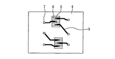
【0033】
図2は、本発明の一実施形態である検査装置の一方の面からみた平面図である。また、図3は、本発明の一実施形態である検査装置の他方の面からみた平面図である。
図3において、シリコン基板4の他方の面の左端上領域と、右端下領域とに分割して複数の梁6が形成されている。そして、これら複数の梁のそれぞれにプローブ5が形成されている。これら複数のプローブ5が、半導体装置のBIST専用パッド3a及び共用パッド3bに接触するように、これらパッド3a及び3bの位置に対応する位置に配置されている。
【0034】
プローブ5は、金属配線9と接続され、この金属配線9は、貫通孔7を介して、シリコン基板4の一方の面に延びている。
【0035】
そして、図2に示すように、金属配線9は、2次電極パッド8に接続される。この2次電極パッド8には、検査信号発生回路(図示せず)からの検査信号が供給される。
【0036】
さて、一般に半導体装置は次のような検査を受けるが、この検査は、半導体基板上に形成された複数の検査用パッド3a、3bと、テスタとの導通を得ることにより行われる。
【0037】
P検と呼ばれる各素子の電気信号の導通を検査するものや、バーンインと呼ばれる、回路に熱的、電気的ストレスを付与して不良を加速選別するものなどがある。P検は通常、プローブ装置を用いて各プローブを回路中の電極パッドに一つずつ接触させて行われる。
【0038】
一方、バーンイン検査では、BIST回路10を用いることにより、検査に必要なパッドを1チップあたり6個程度に抑えることができる。BIST回路とは、半導体装置自体に予め作り込まれた、検査を行うための回路のことをいい、ここでは最低限検査に必要な電源線と信号線のみをまとめて引き出すための回路である。
【0039】
上述したような検査が図2及び図3に示した検査装置により行われる。
【0040】
以上のように、本発明の一実施形態である半導体装置によれば、入出力用の多数のパッドを半導体装置の両端部に分割して配列し、これら多数のパッドのうち、BIST用のパッドの配置領域を半導体装置の一方端の上領域と他方端の下領域とに分割して配置し、一方の領域に配置されるBIST用のパッドを、他の用途と共用とされる。
【0041】
これにより、チップサイズが縮小化され、パッドピッチが縮小化された半導体装置であっても、検査装置により有効に検査可能な半導体装置を実現することができる。
【0042】
また、半導体装置の検査装置において、多数の梁を、シリコン基板の左端上領域と、右端下領域とに分けて配置することにより、つまり、多数の梁を、2つの群に分割し、上記シリコン基板を、このシリコン基板の四隅のうちの一つをそれぞれ含む4つの領域に分割したとき、対角配置となる領域であって、プローブがシリコン基板の端部領域に位置するように形成することにより、シリコン基板の上領域のみ、又は下領域のみに多数の梁を形成する必要はなく、強度的な問題は解消し、検査装置の制作上の困難性も解消することができる。
【0043】
したがって、チップサイズが縮小化され、パッドピッチが縮小化された半導体装置であっても、有効に検査可能な検査装置を実現することができる。
【0044】
さて、複数の半導体装置を複数の検査装置により、一括して検査する方式、つまり、チップ単位に切断される前の、ウエハ上の複数の半導体装置を複数の検査装置により検査する方式が近年採用されている。
【0045】
この場合の、本発明の他の実施形態である検査装置について説明する。
図4は、本発明の一実施形態である半導体装置1が複数個配置されて、検査される場合の状態の説明図である。
【0046】
複数の半導体装置1は互いに隣接して配置され、一つの検査装置により、一方の半導体装置1の共用パッド3bと隣接する他方の半導体装置1のBIST専用パッド3aとが検査される。
【0047】
図5は、本発明の他の実施形態である検査装置の一方の面の平面図であり、図6は、本発明の上記他の実施形態である検査装置の他方の面の平面図である。
【0048】
図6において、シリコン基板4の他方の面の中央左側上領域と、中央右側下領域とに分割して複数の梁6が形成されている。そして、これら複数の梁6のそれぞれにプローブ5が形成されている。これら複数のプローブ5が、一方の半導体装置1のBIST専用パッド3a及び他方の半導体装置1の共用パッド3bに接触するように、これらパッド3a及び3bの位置に対応する位置に配置されている。
【0049】
つまり、多数の梁6は、2つの群に分割され、基板4を、この基板4の四隅のうちの一つをそれぞれ含む4つの領域に分割したとき、対角配置となる領域であって、プローブ5が基板の中央領域の近辺に位置するように形成される。
【0050】
プローブ5は、金属配線9と接続され、この金属配線9は、貫通孔7を介して、シリコン基板4の一方の面に延びている。
【0051】
そして、図5に示すように、金属配線9は、シリコン基板4の両端側に配置された2次電極パッド8に接続される。この2次電極パッド8には、検査信号発生回路(図示せず)からの検査信号が供給される。
【0052】
以上のように、本発明の他の実施形態である検査装置によれば、チップサイズが縮小化され、パッドピッチが縮小化された半導体装置であっても、有効に検査可能な検査装置を実現することができる。
【0053】
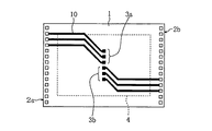
図7は、本発明の他の実施形態である半導体装置のパッド位置の説明図である。図7において、半導体基板1の両端部には、複数のパッド2a、2bが形成されている。
【0054】
そして、半導体装置1の中央部には、BIST専用パッド3a(プローブ接触用パッド)と、共用パッド3b(プローブ接触用パッド)とが形成されており、BIST専用パッド3aは、半導体装置1の左端上領域のパッド2aに配線10により接続され、共用パッド3bは、半導体装置1の右端下領域のパッド2bに配線10により接続されている。
【0055】
この図7の例は、半導体装置1の中央領域にパッド3a、3bを形成可能な空き領域が存在する場合やWPP(Wafer Process Package)のように、半導体装置上にさらに一層再配線層を形成し、半導体装置の中央領域にパッドを形成可能な場合の例である。
【0056】
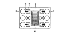
図8は、図7に示した半導体装置1を検査するための検査装置であって、本発明のさらに他の実施形態である検査装置の一方の面の平面図であり、図9は、図8に示した検査装置の他方の面の平面図である。
【0057】
図9において、シリコン基板4の他方の面の中央領域に複数の梁6が形成されている。そして、これら複数の梁6のそれぞれにプローブ5が形成されている。これら複数のプローブ5が、半導体装置1のBIST専用パッド3a及び共用パッド3bに接触するように、これらパッド3a及び3bの位置に対応する位置に配置されている。
【0058】
プローブ5は、金属配線9と接続され、この金属配線9は、貫通孔7を介して、シリコン基板4の一方の面に延びている。
【0059】
そして、図8に示すように、金属配線9は、シリコン基板4の両端側に配置された2次電極パッド8に接続される。この2次電極パッド8には、検査信号発生回路(図示せず)からの検査信号が供給される。
【0060】
以上のように、本発明の他の実施形態である半導体装置によれば、チップサイズが縮小化され、パッドピッチが縮小化された半導体装置であっても、有効に検査可能な検査装置を実現することができる。
【0061】
また、チップサイズが縮小化され、パッドピッチが縮小化された半導体装置であっても、有効に検査可能な検査装置を実現することができる。
【0062】
また、本発明のさらに他の実施形態である検査装置によれば、多数の梁6が2箇所に分割されず形成されるので、検査装置全体の面積を小さくすることができ、検査のための位置決めスペースを多く確保することができる。
【0063】
なお、本発明の実施形態である半導体装置において、入出力パッド群2a、2bは、半導体基板2の端面からどの位の位置まで形成し得るかにより、パッドの形成領域が決定され、形成し得るパッドの数も決定される。本発明の実子形態においては、半導体基板2の端面から1パッド分の寸法まで、パッドを形成し得る領域とすることができる。
【0064】
【発明の効果】
本発明によれば、チップサイズが縮小化され、パッドピッチが縮小化された半導体装置であっても、検査装置により有効に検査可能な半導体装置及びその検査装置を実現することができる。
【図面の簡単な説明】
【図1】本発明の一実施形態である半導体装置のパッド位置の説明図である。
【図2】本発明の一実施形態である検査装置の一方の面からみた平面図である。
【図3】本発明の一実施形態である検査装置の他方の面からみた平面図である。
【図4】本発明の他の実施形態である検査装置の説明図である。
【図5】本発明の他の実施形態である検査装置の一方の面からみた平面図である。
【図6】本発明の他の実施形態である検査装置の他方の面からみた平面図である。
【図7】本発明の他の実施形態である半導体装置のパッド位置の説明図である。
【図8】本発明のさらに他の実施形態である検査装置の一方の面からみた平面図である。
【図9】本発明のさらに他の実施形態である検査装置の他方の面からみた平面図である。
【符号の説明】
1 半導体装置基板
2a、2b パッド群
3a BIST専用パッド
3b 共用パッド
4 シリコン基板
5 プローブ
6 梁
7 貫通孔
8 2次電極パッド
9 配線
10 BIST回路[0001]
BACKGROUND OF THE INVENTION
The present invention relates to a semiconductor device and an inspection device thereof.
[0002]
[Prior art]
Reflecting high-density mounting and high functionality of electronic devices using semiconductor devices, there is an increasing demand for high integration of the semiconductor devices themselves.
[0003]
In general, high integration of a semiconductor device is achieved by miniaturization of circuit elements constituting the semiconductor device. That is, high integration can be achieved by microfabrication of wirings or connection holes constituting circuit elements.
[0004]
On the other hand, in order to reduce the cost of the semiconductor device and improve the yield, a technique for increasing the number of semiconductor chips formed in one wafer as much as possible is required. That is, a technique for optimizing and miniaturizing the design and manufacturing process is required so that circuits capable of realizing the same function can be realized with as small a chip area as possible.
[0005]
For example, a product group of the same generation that realizes the same function, such as a DRAM (Dynamic Random Access Memory), is designed under relatively loose design rules at the initial stage of market introduction. For this reason, the chip size is relatively large and the cost is correspondingly higher.
[0006]
However, in the middle or late stage of market introduction, as a result of miniaturization efforts, the chip size is reduced, and the cost per chip is reduced and the yield is improved at the same time.
[0007]
Such chip size reduction is performed over several orders in the same generation product group, and the chip size reduction is repeated every time the product generation changes. As a result, the wiring pattern formed on the chip surface is simultaneously reduced, and accordingly, the size and pad pitch of the inspection pads for inspecting the semiconductor device are inevitably reduced.
[0008]
Thus, due to the reduction in the pad pitch and the increase in the number of inspection pads due to the increase in the number of chips per wafer, it is difficult to inspect with the conventional inspection methods.
[0009]
Therefore, as described in Japanese Patent Laid-Open No. 11-274251, probes, beams, wirings, and secondary electrode pads are formed on the inspection substrate on the same silicon substrate as the semiconductor device, and are formed on each of the plurality of beams. A method has been developed in which a protruding probe is in contact with a predetermined pad formed on a semiconductor device for inspection.
[0010]
In addition, as described in Japanese Patent Application Laid-Open No. 2000-227459, there is a device in which a BIST (Built-In Self Test) circuit is incorporated in a semiconductor chip so that a simple inspection can be performed.
[0011]
[Problems to be solved by the invention]
However, higher integration in semiconductor devices is desired, and with the increase in the number of pads and the reduction in arrangement area, further reduction in pad pitch is necessary. There is a risk that it may be difficult to manufacture an inspection substrate for an inspection apparatus that can cope with the above.
[0012]
In other words, as described above, the inspection apparatus for a semiconductor device has a probe, a beam, a wiring, and a secondary electrode pad formed on a silicon substrate. It is necessary to reduce the width, and if the arrangement of the pads is the same as in the conventional case, a plurality of beams formed corresponding to this have a problem in strength, and it is difficult to produce.
[0013]
An object of the present invention is to realize a semiconductor device that can be effectively inspected by an inspection apparatus and the inspection apparatus even if the semiconductor device has a reduced chip size and a reduced pad pitch.
[0014]
[Means for Solving the Problems]
In order to achieve the above object, the present invention is configured as follows.
(1) In a semiconductor device having a plurality of input / output pads on a main surface of a semiconductor substrate, the semiconductor device includes a BIST circuit, and the plurality of input / output pads are divided at both ends of the main surface, Arranged in a row, the plurality of pads include a plurality of inspection pads used for electrical inspection of the semiconductor device, the inspection pads are divided into two groups, and the main surface is divided into four corners of the main surface. When divided into four areas each including one of them, the plurality of pads formed in the diagonally arranged areas include each of the two divided inspection pads , and the pair The inspection pads formed in any one of the corner arrangement regions are dedicated pads for the BIST circuit.
[0015]
(2) A plurality of beams, probes formed on each of the plurality of beams and in contact with pads for electrical inspection formed on the semiconductor device, and electrically connected to these probes via connection lines And a substrate having a plurality of secondary electrode pads for signal input / output, and inspecting the semiconductor device according to (1) above, the plurality of beams are divided into two groups. When the substrate is divided into four regions each including one of the four corners of the substrate, the substrate is formed in a diagonal arrangement, and the probe is positioned in the end region of the substrate. The
[0016]
(3) A plurality of beams, probes formed on each of the plurality of beams and in contact with pads for electrical inspection formed on the semiconductor device, and electrically connected to these probes via connection lines And a substrate having a plurality of secondary electrode pads for signal input / output, and inspecting the semiconductor device according to ( 1 ) above, the plurality of beams are divided into two groups. When the substrate is divided into four regions each including one of the four corners of the substrate, it is a region that is diagonally arranged and that the probe is positioned in the vicinity of the central region of the substrate. Is done.
[0019]
When the inspection pads are formed in the diagonal region of the semiconductor device, the plurality of beams on which the inspection device probes for contacting the inspection pads are divided into two diagonal regions. Can do. If the plurality of beams are arranged opposite to each other instead of diagonally, there is a problem in strength, and it is difficult to produce an inspection apparatus.
[0020]
By forming the beams in the diagonally arranged region, the problem of the strength of the substrate in the inspection apparatus can be solved, and the difficulty in producing the inspection apparatus can also be eliminated.
[0021]
DETAILED DESCRIPTION OF THE INVENTION
Embodiments of the present invention will be described below with reference to the accompanying drawings.
FIG. 1 is an explanatory diagram of pad positions of a semiconductor device according to an embodiment of the present invention. In FIG. 1, a plurality of
[0022]
The
[0023]
Also, a BIST (Built-In Self Test)
[0024]
Here, a large number of BIST pads are required. However, as described above, as the number of input pads and the like increases, the area where the BIST pads are arranged is limited, and all the BIST pads are placed in the semiconductor device 1. They cannot be arranged in a row on one end side.
[0025]
For this reason, the BIST pad arrangement area is divided into both ends of the semiconductor device, and those arranged in the vicinity of the
[0026]
Furthermore, the BIST
[0027]
The reason is that if the BIST-dedicated
[0028]
If all of the many beams are formed in the upper region of the inspection apparatus, there is a problem in strength, and it becomes difficult to produce the inspection apparatus.
[0029]
Therefore, the BIST-dedicated
[0030]
Here, the upper left end region is an end side region from the position of the distance of one pad to the size of one or two pads as measured from the left end surface of the semiconductor substrate 1 in FIG. The upper region when the semiconductor substrate 1 is divided into two in the vertical direction in FIG.
[0031]
Further, the lower right end region is an end portion side region from the position of the distance corresponding to one pad to the size corresponding to one or two pads as measured from the right end surface on the semiconductor substrate 1 in FIG. A lower region when the semiconductor substrate 1 is divided into two in the vertical direction in FIG.
[0032]
Therefore, the
[0033]
FIG. 2 is a plan view seen from one surface of the inspection apparatus according to one embodiment of the present invention. FIG. 3 is a plan view seen from the other surface of the inspection apparatus according to the embodiment of the present invention.
In FIG. 3, a plurality of
[0034]
The
[0035]
As shown in FIG. 2, the
[0036]
In general, a semiconductor device is subjected to the following inspection. This inspection is performed by obtaining electrical continuity between a plurality of
[0037]
There is a method called a P test for checking the electrical signal conduction of each element, and a method called burn-in for applying a thermal or electrical stress to a circuit and accelerating selection of defects. The P test is usually performed by using a probe device to bring each probe into contact with an electrode pad in the circuit one by one.
[0038]
On the other hand, in the burn-in inspection, by using the
[0039]
The inspection as described above is performed by the inspection apparatus shown in FIGS.
[0040]
As described above, according to the semiconductor device of one embodiment of the present invention, a large number of input / output pads are divided and arranged at both ends of the semiconductor device, and among these many pads, a BIST pad is arranged. The arrangement area is divided into an upper area at one end and a lower area at the other end of the semiconductor device, and the BIST pads arranged in one area are shared with other applications.
[0041]
As a result, it is possible to realize a semiconductor device that can be effectively inspected by the inspection apparatus even if the semiconductor device has a reduced chip size and a reduced pad pitch.
[0042]
Further, in a semiconductor device inspection apparatus, a large number of beams are divided into an upper left end region and a lower right end region of a silicon substrate, that is, a large number of beams are divided into two groups. When the substrate is divided into four regions each including one of the four corners of the silicon substrate, it is formed so as to be a diagonally arranged region in which the probe is located in the end region of the silicon substrate. Therefore, it is not necessary to form a large number of beams only in the upper region or only in the lower region of the silicon substrate, the strength problem can be solved, and the difficulty in producing the inspection apparatus can be solved.
[0043]
Therefore, it is possible to realize an inspection apparatus that can effectively inspect even a semiconductor device in which the chip size is reduced and the pad pitch is reduced.
[0044]
In recent years, a system in which a plurality of semiconductor devices are inspected collectively by a plurality of inspection apparatuses, that is, a system in which a plurality of semiconductor devices on a wafer before being cut into chips is inspected by a plurality of inspection apparatuses has been adopted. Has been.
[0045]
An inspection apparatus according to another embodiment of the present invention in this case will be described.
FIG. 4 is an explanatory diagram of a state where a plurality of semiconductor devices 1 according to an embodiment of the present invention are arranged and inspected.
[0046]
The plurality of semiconductor devices 1 are disposed adjacent to each other, and the
[0047]
FIG. 5 is a plan view of one surface of an inspection apparatus according to another embodiment of the present invention, and FIG. 6 is a plan view of the other surface of the inspection apparatus according to another embodiment of the present invention. .
[0048]
In FIG. 6, a plurality of
[0049]
That is, the
[0050]
The
[0051]
Then, as shown in FIG. 5, the
[0052]
As described above, according to the inspection apparatus of another embodiment of the present invention, an inspection apparatus that can effectively inspect even a semiconductor device with a reduced chip size and a reduced pad pitch is realized. can do.
[0053]
FIG. 7 is an explanatory diagram of pad positions of a semiconductor device according to another embodiment of the present invention. In FIG. 7, a plurality of
[0054]
A BIST
[0055]
In the example of FIG. 7, a redistribution layer is further formed on the semiconductor device, such as when there is a vacant region in which the
[0056]
8 is an inspection apparatus for inspecting the semiconductor device 1 shown in FIG. 7, and is a plan view of one surface of an inspection apparatus which is still another embodiment of the present invention. FIG. 9 is a plan view of the other surface of the inspection apparatus shown in FIG.
[0057]
In FIG. 9, a plurality of
[0058]
The
[0059]
As shown in FIG. 8, the
[0060]
As described above, according to the semiconductor device of another embodiment of the present invention, an inspection apparatus capable of effectively inspecting even when the semiconductor device has a reduced chip size and a reduced pad pitch is realized. can do.
[0061]
Further, it is possible to realize an inspection apparatus that can effectively inspect even a semiconductor device in which the chip size is reduced and the pad pitch is reduced.
[0062]
Further, according to the inspection apparatus which is still another embodiment of the present invention, since the
[0063]
In the semiconductor device according to the embodiment of the present invention, the input /
[0064]
【The invention's effect】
ADVANTAGE OF THE INVENTION According to this invention, even if it is a semiconductor device with which chip size was reduced and the pad pitch was reduced, the semiconductor device which can be test | inspected effectively with an inspection apparatus, and its inspection apparatus are realizable.
[Brief description of the drawings]
FIG. 1 is an explanatory diagram of pad positions of a semiconductor device according to an embodiment of the present invention.
FIG. 2 is a plan view seen from one surface of an inspection apparatus according to an embodiment of the present invention.
FIG. 3 is a plan view seen from the other surface of the inspection apparatus according to the embodiment of the present invention.
FIG. 4 is an explanatory diagram of an inspection apparatus according to another embodiment of the present invention.
FIG. 5 is a plan view seen from one surface of an inspection apparatus according to another embodiment of the present invention.
FIG. 6 is a plan view seen from the other surface of an inspection apparatus according to another embodiment of the present invention.
FIG. 7 is an explanatory diagram of pad positions of a semiconductor device according to another embodiment of the present invention.
FIG. 8 is a plan view seen from one surface of an inspection apparatus according to still another embodiment of the present invention.
FIG. 9 is a plan view seen from the other surface of an inspection apparatus according to still another embodiment of the present invention.
[Explanation of symbols]
DESCRIPTION OF SYMBOLS 1
Claims (3)
BIST回路を備え、
上記複数の入出力用のパッドは、上記主面の両端部に分割して、少なくとも一列に配置され、これら複数のパッドは半導体装置の電気的検査に用いられる複数の検査用パッドを含み、これら検査用パッドは2つの群に分割され、上記主面を、この主面の四隅のうちの一つをそれぞれ含む4つの領域に分割したとき、対角配置となる領域に形成された複数のパッドに、上記2つに分割された検査用パッドのそれぞれが含まれ、かつ、上記対角配置となる領域のいずれか一方の領域に形成された検査用パッドは上記BIST回路専用のパッドであることを特徴とする半導体装置。In a semiconductor device having a plurality of input / output pads on a main surface of a semiconductor substrate,
A BIST circuit,
The plurality of input / output pads are divided into both ends of the main surface and arranged in at least one row, and the plurality of pads include a plurality of inspection pads used for electrical inspection of a semiconductor device. The inspection pads are divided into two groups, and when the main surface is divided into four regions each including one of the four corners of the main surface, a plurality of pads formed in regions that are diagonally arranged Each of the test pads divided into two, and the test pad formed in one of the diagonally arranged regions is a pad dedicated to the BIST circuit. A semiconductor device characterized by the above.
上記複数の梁は、2つの群に分割され、上記基板を、この基板の四隅のうちの一つをそれぞれ含む4つの領域に分割したとき、対角配置となる領域であって、上記プローブが基板の端部領域に位置するように形成されることを特徴とする半導体装置の検査装置。A plurality of beams, probes formed on each of the plurality of beams and in contact with pads for electrical inspection formed on the semiconductor device, and signals electrically connected to these probes through connection lines comprising a substrate and a plurality of secondary electrode pads for the input and output, in the inspection the inspection apparatus for performing a semiconductor device according to claim 1,
The plurality of beams are divided into two groups. When the substrate is divided into four regions each including one of the four corners of the substrate, the beams are diagonally arranged, and the probe is An inspection apparatus for a semiconductor device, wherein the inspection apparatus is formed so as to be positioned in an end region of a substrate.
上記複数の梁は、2つの群に分割され、上記基板を、この基板の四隅のうちの一つをそれぞれ含む4つの領域に分割したとき、対角配置となる領域であって、上記プローブが基板の中央領域の近辺に位置するように形成されることを特徴とする半導体装置の検査装置。A plurality of beams, probes formed on each of the plurality of beams and in contact with pads for electrical inspection formed on the semiconductor device, and signals electrically connected to these probes through connection lines comprising a substrate and a plurality of secondary electrode pads for the input and output, in the inspection the inspection apparatus for performing a semiconductor device according to claim 1,
The plurality of beams are divided into two groups. When the substrate is divided into four regions each including one of the four corners of the substrate, the beams are diagonally arranged, and the probe is An inspection apparatus for a semiconductor device, wherein the inspection apparatus is formed so as to be positioned near a central region of a substrate.
Priority Applications (5)
| Application Number | Priority Date | Filing Date | Title |
|---|---|---|---|
| JP2001276530A JP4041663B2 (en) | 2001-09-12 | 2001-09-12 | Semiconductor device and its inspection device |
| TW091113300A TW546756B (en) | 2001-09-12 | 2002-06-18 | Semiconductor device and test device thereof |
| US10/218,596 US6885208B2 (en) | 2001-09-12 | 2002-08-15 | Semiconductor device and test device for same |
| CNB021421846A CN1213470C (en) | 2001-09-12 | 2002-08-29 | Semiconductor device and checkup apparatus thereof |
| KR10-2002-0054725A KR100467913B1 (en) | 2001-09-12 | 2002-09-10 | Semiconductor apparatus and thereof apparatus |
Applications Claiming Priority (1)
| Application Number | Priority Date | Filing Date | Title |
|---|---|---|---|
| JP2001276530A JP4041663B2 (en) | 2001-09-12 | 2001-09-12 | Semiconductor device and its inspection device |
Publications (2)
| Publication Number | Publication Date |
|---|---|
| JP2003084042A JP2003084042A (en) | 2003-03-19 |
| JP4041663B2 true JP4041663B2 (en) | 2008-01-30 |
Family
ID=19101212
Family Applications (1)
| Application Number | Title | Priority Date | Filing Date |
|---|---|---|---|
| JP2001276530A Expired - Fee Related JP4041663B2 (en) | 2001-09-12 | 2001-09-12 | Semiconductor device and its inspection device |
Country Status (5)
| Country | Link |
|---|---|
| US (1) | US6885208B2 (en) |
| JP (1) | JP4041663B2 (en) |
| KR (1) | KR100467913B1 (en) |
| CN (1) | CN1213470C (en) |
| TW (1) | TW546756B (en) |
Families Citing this family (8)
| Publication number | Priority date | Publication date | Assignee | Title |
|---|---|---|---|---|
| US7342248B2 (en) | 2003-05-15 | 2008-03-11 | Shinko Electric Industries Co., Ltd. | Semiconductor device and interposer |
| KR20050011082A (en) * | 2003-07-21 | 2005-01-29 | 매그나칩 반도체 유한회사 | Semiconductor device with extension internal probing pad |
| JP2005136246A (en) * | 2003-10-31 | 2005-05-26 | Renesas Technology Corp | Manufacturing method of semiconductor integrate circuit device |
| BRPI0620316A2 (en) * | 2005-12-21 | 2011-11-08 | Wyeth Corp | Low viscosity protein formulations and their uses |
| US8399973B2 (en) * | 2007-12-20 | 2013-03-19 | Mosaid Technologies Incorporated | Data storage and stackable configurations |
| KR101212723B1 (en) * | 2010-05-31 | 2012-12-14 | 에스케이하이닉스 주식회사 | Semiconductor Apparatus |
| KR102107147B1 (en) | 2013-02-01 | 2020-05-26 | 삼성전자주식회사 | Package on package device |
| CN108206140B (en) * | 2016-12-19 | 2020-11-24 | 中芯国际集成电路制造(上海)有限公司 | Semiconductor device, manufacturing method thereof and electronic device |
Family Cites Families (19)
| Publication number | Priority date | Publication date | Assignee | Title |
|---|---|---|---|---|
| CA954635A (en) * | 1972-06-06 | 1974-09-10 | Microsystems International Limited | Mounting leads and method of fabrication |
| JPS61148829A (en) * | 1984-12-24 | 1986-07-07 | Toshiba Seiki Kk | Wire bonding method |
| JPS63148829A (en) * | 1986-12-11 | 1988-06-21 | 古河電池株式会社 | Constant current circuit |
| JPH04174538A (en) * | 1990-08-02 | 1992-06-22 | Hitachi Ltd | Manufacture of semiconductor integrated circuit device |
| JPH04278560A (en) * | 1991-03-07 | 1992-10-05 | Nec Yamagata Ltd | Manufacture of semiconductor device |
| JPH09107048A (en) * | 1995-03-30 | 1997-04-22 | Mitsubishi Electric Corp | Semiconductor package |
| US5929650A (en) * | 1997-02-04 | 1999-07-27 | Motorola, Inc. | Method and apparatus for performing operative testing on an integrated circuit |
| JPH1154562A (en) * | 1997-08-05 | 1999-02-26 | Shinko Electric Ind Co Ltd | Semiconductor package |
| US6427222B1 (en) * | 1997-09-30 | 2002-07-30 | Jeng-Jye Shau | Inter-dice wafer level signal transfer methods for integrated circuits |
| JPH11243120A (en) * | 1998-02-25 | 1999-09-07 | Matsushita Electron Corp | Semiconductor device and its manufacture |
| JP4006081B2 (en) | 1998-03-19 | 2007-11-14 | 株式会社ルネサステクノロジ | Manufacturing method of semiconductor device |
| JPH11281757A (en) * | 1998-03-30 | 1999-10-15 | Fujitsu Ltd | Atmospheric pollutant measurement system |
| US6061814A (en) * | 1998-04-21 | 2000-05-09 | Lsi Logic Corporation | Test circuitry for determining the defect density of a semiconductor process as a function of individual metal layers |
| US6456099B1 (en) * | 1998-12-31 | 2002-09-24 | Formfactor, Inc. | Special contact points for accessing internal circuitry of an integrated circuit |
| JP2000227459A (en) | 1999-02-05 | 2000-08-15 | Sharp Corp | Semiconductor integrated circuit, its test method, and probe jig used for test |
| JP2000332077A (en) | 1999-05-17 | 2000-11-30 | Sony Corp | Method and structure for inspecting wiring defect of semiconductor integrated circuit |
| JP2001091543A (en) * | 1999-09-27 | 2001-04-06 | Hitachi Ltd | Semiconductor inspecting device |
| JP2002110751A (en) * | 2000-10-03 | 2002-04-12 | Hitachi Ltd | Apparatus for inspecting semiconductor integrated circuit device, and its manufacturing method |
| JP2003208686A (en) * | 2002-01-10 | 2003-07-25 | Moritoshi Sato | Air pollution observation data transmission/reception system |
-
2001
- 2001-09-12 JP JP2001276530A patent/JP4041663B2/en not_active Expired - Fee Related
-
2002
- 2002-06-18 TW TW091113300A patent/TW546756B/en not_active IP Right Cessation
- 2002-08-15 US US10/218,596 patent/US6885208B2/en not_active Expired - Fee Related
- 2002-08-29 CN CNB021421846A patent/CN1213470C/en not_active Expired - Fee Related
- 2002-09-10 KR KR10-2002-0054725A patent/KR100467913B1/en not_active IP Right Cessation
Also Published As
| Publication number | Publication date |
|---|---|
| US6885208B2 (en) | 2005-04-26 |
| KR20030023510A (en) | 2003-03-19 |
| JP2003084042A (en) | 2003-03-19 |
| CN1213470C (en) | 2005-08-03 |
| KR100467913B1 (en) | 2005-01-24 |
| US20030047731A1 (en) | 2003-03-13 |
| TW546756B (en) | 2003-08-11 |
| CN1404123A (en) | 2003-03-19 |
Similar Documents
| Publication | Publication Date | Title |
|---|---|---|
| JP3135825B2 (en) | Probe card and probing test method for semiconductor integrated circuit using the probe card | |
| US5262719A (en) | Test structure for multi-layer, thin-film modules | |
| JP2005209239A (en) | Semiconductor integrated circuit apparatus | |
| JP2008527328A (en) | Probe head array | |
| JP4041663B2 (en) | Semiconductor device and its inspection device | |
| US20070035318A1 (en) | Donut-type parallel probe card and method of testing semiconductor wafer using same | |
| US4778771A (en) | Process of forming input/output wiring areas for semiconductor integrated circuit | |
| CN110531125B (en) | Space transformer, probe card and manufacturing method thereof | |
| US20080106279A1 (en) | Probe card layout | |
| EP0374466B1 (en) | In-line process monitors for thin film wiring | |
| US7535239B1 (en) | Probe card configured for interchangeable heads | |
| JP3453526B2 (en) | Semiconductor element inspection socket, semiconductor device, semiconductor device manufacturing method, and semiconductor device inspection method | |
| KR100798724B1 (en) | Method for wafer test and probe card for the same | |
| US9069015B2 (en) | Interface board of a testing head for a test equipment of electronic devices and corresponding probe head | |
| KR200423446Y1 (en) | Probe card | |
| KR100679167B1 (en) | The probe card using coaxial cable for semiconductor wafer | |
| KR100519658B1 (en) | Probe card | |
| JPH05206383A (en) | Semiconductor wafer and method for inspecting the same | |
| JP5333829B2 (en) | Probe assembly | |
| KR20050029066A (en) | Probe card | |
| KR100794629B1 (en) | Apparatus for inspecting electric condition and method for manufacturing the same | |
| JP7488492B2 (en) | Semiconductor Wafers | |
| EP2872906B1 (en) | Interface board of a testing head for a test equipment of electronic devices and corresponding testing head | |
| JP2001077162A (en) | Probing test method for semiconductor integrated circuit | |
| KR100906498B1 (en) | Merged Memory and Logic Device |
Legal Events
| Date | Code | Title | Description |
|---|---|---|---|
| A621 | Written request for application examination |
Free format text: JAPANESE INTERMEDIATE CODE: A621 Effective date: 20041026 |
|
| A977 | Report on retrieval |
Free format text: JAPANESE INTERMEDIATE CODE: A971007 Effective date: 20050822 |
|
| A131 | Notification of reasons for refusal |
Free format text: JAPANESE INTERMEDIATE CODE: A131 Effective date: 20070731 |
|
| A521 | Request for written amendment filed |
Free format text: JAPANESE INTERMEDIATE CODE: A523 Effective date: 20070927 |
|
| TRDD | Decision of grant or rejection written | ||
| A01 | Written decision to grant a patent or to grant a registration (utility model) |
Free format text: JAPANESE INTERMEDIATE CODE: A01 Effective date: 20071106 |
|
| A61 | First payment of annual fees (during grant procedure) |
Free format text: JAPANESE INTERMEDIATE CODE: A61 Effective date: 20071112 |
|
| FPAY | Renewal fee payment (event date is renewal date of database) |
Free format text: PAYMENT UNTIL: 20101116 Year of fee payment: 3 |
|
| R150 | Certificate of patent or registration of utility model |
Free format text: JAPANESE INTERMEDIATE CODE: R150 |
|
| FPAY | Renewal fee payment (event date is renewal date of database) |
Free format text: PAYMENT UNTIL: 20111116 Year of fee payment: 4 |
|
| FPAY | Renewal fee payment (event date is renewal date of database) |
Free format text: PAYMENT UNTIL: 20111116 Year of fee payment: 4 |
|
| S111 | Request for change of ownership or part of ownership |
Free format text: JAPANESE INTERMEDIATE CODE: R313111 |
|
| FPAY | Renewal fee payment (event date is renewal date of database) |
Free format text: PAYMENT UNTIL: 20111116 Year of fee payment: 4 |
|
| R350 | Written notification of registration of transfer |
Free format text: JAPANESE INTERMEDIATE CODE: R350 |
|
| FPAY | Renewal fee payment (event date is renewal date of database) |
Free format text: PAYMENT UNTIL: 20111116 Year of fee payment: 4 |
|
| FPAY | Renewal fee payment (event date is renewal date of database) |
Free format text: PAYMENT UNTIL: 20121116 Year of fee payment: 5 |
|
| FPAY | Renewal fee payment (event date is renewal date of database) |
Free format text: PAYMENT UNTIL: 20121116 Year of fee payment: 5 |
|
| FPAY | Renewal fee payment (event date is renewal date of database) |
Free format text: PAYMENT UNTIL: 20131116 Year of fee payment: 6 |
|
| S531 | Written request for registration of change of domicile |
Free format text: JAPANESE INTERMEDIATE CODE: R313531 |
|
| R350 | Written notification of registration of transfer |
Free format text: JAPANESE INTERMEDIATE CODE: R350 |
|
| LAPS | Cancellation because of no payment of annual fees |