JP4036923B2 - Display device and drive circuit thereof - Google Patents
Display device and drive circuit thereof Download PDFInfo
- Publication number
- JP4036923B2 JP4036923B2 JP20857097A JP20857097A JP4036923B2 JP 4036923 B2 JP4036923 B2 JP 4036923B2 JP 20857097 A JP20857097 A JP 20857097A JP 20857097 A JP20857097 A JP 20857097A JP 4036923 B2 JP4036923 B2 JP 4036923B2
- Authority
- JP
- Japan
- Prior art keywords
- channel
- tft
- type tft
- drain
- power supply
- Prior art date
- Legal status (The legal status is an assumption and is not a legal conclusion. Google has not performed a legal analysis and makes no representation as to the accuracy of the status listed.)
- Expired - Fee Related
Links
- 239000004973 liquid crystal related substance Substances 0.000 claims description 103
- 239000000758 substrate Substances 0.000 claims description 43
- 239000004065 semiconductor Substances 0.000 claims description 23
- 238000005401 electroluminescence Methods 0.000 claims description 2
- 239000010408 film Substances 0.000 description 66
- 239000010410 layer Substances 0.000 description 37
- 239000011159 matrix material Substances 0.000 description 27
- 238000000034 method Methods 0.000 description 26
- 238000010586 diagram Methods 0.000 description 17
- PXHVJJICTQNCMI-UHFFFAOYSA-N Nickel Chemical compound [Ni] PXHVJJICTQNCMI-UHFFFAOYSA-N 0.000 description 16
- 239000012535 impurity Substances 0.000 description 16
- 238000010438 heat treatment Methods 0.000 description 12
- 229910021417 amorphous silicon Inorganic materials 0.000 description 10
- 238000004519 manufacturing process Methods 0.000 description 10
- 230000002093 peripheral effect Effects 0.000 description 10
- 239000012298 atmosphere Substances 0.000 description 9
- 230000003287 optical effect Effects 0.000 description 9
- 230000008569 process Effects 0.000 description 9
- 230000015556 catabolic process Effects 0.000 description 8
- 229910052736 halogen Inorganic materials 0.000 description 8
- 150000002367 halogens Chemical class 0.000 description 8
- VYPSYNLAJGMNEJ-UHFFFAOYSA-N silicon dioxide Inorganic materials O=[Si]=O VYPSYNLAJGMNEJ-UHFFFAOYSA-N 0.000 description 8
- 239000010409 thin film Substances 0.000 description 8
- 239000000872 buffer Substances 0.000 description 7
- 230000008859 change Effects 0.000 description 7
- 238000002425 crystallisation Methods 0.000 description 7
- 230000008025 crystallization Effects 0.000 description 7
- 230000007547 defect Effects 0.000 description 7
- 229910052759 nickel Inorganic materials 0.000 description 7
- 239000010453 quartz Substances 0.000 description 7
- 238000004088 simulation Methods 0.000 description 7
- 230000015572 biosynthetic process Effects 0.000 description 6
- 230000006866 deterioration Effects 0.000 description 6
- 230000000694 effects Effects 0.000 description 6
- 150000002500 ions Chemical group 0.000 description 6
- 230000004044 response Effects 0.000 description 6
- 229910052581 Si3N4 Inorganic materials 0.000 description 5
- 238000004458 analytical method Methods 0.000 description 5
- 239000000969 carrier Substances 0.000 description 5
- 239000003054 catalyst Substances 0.000 description 5
- 238000005247 gettering Methods 0.000 description 5
- 239000011521 glass Substances 0.000 description 5
- HQVNEWCFYHHQES-UHFFFAOYSA-N silicon nitride Chemical compound N12[Si]34N5[Si]62N3[Si]51N64 HQVNEWCFYHHQES-UHFFFAOYSA-N 0.000 description 5
- IJGRMHOSHXDMSA-UHFFFAOYSA-N Atomic nitrogen Chemical compound N#N IJGRMHOSHXDMSA-UHFFFAOYSA-N 0.000 description 4
- UFHFLCQGNIYNRP-UHFFFAOYSA-N Hydrogen Chemical compound [H][H] UFHFLCQGNIYNRP-UHFFFAOYSA-N 0.000 description 4
- 239000010407 anodic oxide Substances 0.000 description 4
- QVGXLLKOCUKJST-UHFFFAOYSA-N atomic oxygen Chemical compound [O] QVGXLLKOCUKJST-UHFFFAOYSA-N 0.000 description 4
- 239000013078 crystal Substances 0.000 description 4
- 230000005684 electric field Effects 0.000 description 4
- 230000006870 function Effects 0.000 description 4
- 229910052739 hydrogen Inorganic materials 0.000 description 4
- 239000001257 hydrogen Substances 0.000 description 4
- 229910052760 oxygen Inorganic materials 0.000 description 4
- 239000001301 oxygen Substances 0.000 description 4
- ZOXJGFHDIHLPTG-UHFFFAOYSA-N Boron Chemical compound [B] ZOXJGFHDIHLPTG-UHFFFAOYSA-N 0.000 description 3
- VEXZGXHMUGYJMC-UHFFFAOYSA-N Hydrochloric acid Chemical compound Cl VEXZGXHMUGYJMC-UHFFFAOYSA-N 0.000 description 3
- KDLHZDBZIXYQEI-UHFFFAOYSA-N Palladium Chemical compound [Pd] KDLHZDBZIXYQEI-UHFFFAOYSA-N 0.000 description 3
- XUIMIQQOPSSXEZ-UHFFFAOYSA-N Silicon Chemical compound [Si] XUIMIQQOPSSXEZ-UHFFFAOYSA-N 0.000 description 3
- 230000001133 acceleration Effects 0.000 description 3
- 229910052796 boron Inorganic materials 0.000 description 3
- 239000003990 capacitor Substances 0.000 description 3
- 230000003197 catalytic effect Effects 0.000 description 3
- 239000003086 colorant Substances 0.000 description 3
- 150000001875 compounds Chemical class 0.000 description 3
- 239000011229 interlayer Substances 0.000 description 3
- 238000000059 patterning Methods 0.000 description 3
- BASFCYQUMIYNBI-UHFFFAOYSA-N platinum Chemical compound [Pt] BASFCYQUMIYNBI-UHFFFAOYSA-N 0.000 description 3
- 229910052710 silicon Inorganic materials 0.000 description 3
- 239000010703 silicon Substances 0.000 description 3
- OKTJSMMVPCPJKN-UHFFFAOYSA-N Carbon Chemical compound [C] OKTJSMMVPCPJKN-UHFFFAOYSA-N 0.000 description 2
- OAICVXFJPJFONN-UHFFFAOYSA-N Phosphorus Chemical compound [P] OAICVXFJPJFONN-UHFFFAOYSA-N 0.000 description 2
- NINIDFKCEFEMDL-UHFFFAOYSA-N Sulfur Chemical compound [S] NINIDFKCEFEMDL-UHFFFAOYSA-N 0.000 description 2
- 229910052782 aluminium Inorganic materials 0.000 description 2
- XAGFODPZIPBFFR-UHFFFAOYSA-N aluminium Chemical compound [Al] XAGFODPZIPBFFR-UHFFFAOYSA-N 0.000 description 2
- 238000000137 annealing Methods 0.000 description 2
- 229910052799 carbon Inorganic materials 0.000 description 2
- 239000000460 chlorine Substances 0.000 description 2
- 239000010949 copper Substances 0.000 description 2
- 238000006731 degradation reaction Methods 0.000 description 2
- 239000007789 gas Substances 0.000 description 2
- 239000010931 gold Substances 0.000 description 2
- 229910000041 hydrogen chloride Inorganic materials 0.000 description 2
- IXCSERBJSXMMFS-UHFFFAOYSA-N hydrogen chloride Substances Cl.Cl IXCSERBJSXMMFS-UHFFFAOYSA-N 0.000 description 2
- 238000005224 laser annealing Methods 0.000 description 2
- 229910052751 metal Inorganic materials 0.000 description 2
- 239000002184 metal Substances 0.000 description 2
- 229910052757 nitrogen Inorganic materials 0.000 description 2
- 239000012299 nitrogen atmosphere Substances 0.000 description 2
- 238000007254 oxidation reaction Methods 0.000 description 2
- 229910052698 phosphorus Inorganic materials 0.000 description 2
- 239000011574 phosphorus Substances 0.000 description 2
- 229920001721 polyimide Polymers 0.000 description 2
- 229910052717 sulfur Inorganic materials 0.000 description 2
- 239000011593 sulfur Substances 0.000 description 2
- DFGKGUXTPFWHIX-UHFFFAOYSA-N 6-[2-[4-[2-(2,3-dihydro-1H-inden-2-ylamino)pyrimidin-5-yl]piperazin-1-yl]acetyl]-3H-1,3-benzoxazol-2-one Chemical compound C1C(CC2=CC=CC=C12)NC1=NC=C(C=N1)N1CCN(CC1)CC(=O)C1=CC2=C(NC(O2)=O)C=C1 DFGKGUXTPFWHIX-UHFFFAOYSA-N 0.000 description 1
- ZAMOUSCENKQFHK-UHFFFAOYSA-N Chlorine atom Chemical compound [Cl] ZAMOUSCENKQFHK-UHFFFAOYSA-N 0.000 description 1
- RYGMFSIKBFXOCR-UHFFFAOYSA-N Copper Chemical compound [Cu] RYGMFSIKBFXOCR-UHFFFAOYSA-N 0.000 description 1
- XEEYBQQBJWHFJM-UHFFFAOYSA-N Iron Chemical compound [Fe] XEEYBQQBJWHFJM-UHFFFAOYSA-N 0.000 description 1
- 239000004988 Nematic liquid crystal Substances 0.000 description 1
- 229910021586 Nickel(II) chloride Inorganic materials 0.000 description 1
- 239000004642 Polyimide Substances 0.000 description 1
- 230000009471 action Effects 0.000 description 1
- 230000002411 adverse Effects 0.000 description 1
- 229910052785 arsenic Inorganic materials 0.000 description 1
- RQNWIZPPADIBDY-UHFFFAOYSA-N arsenic atom Chemical compound [As] RQNWIZPPADIBDY-UHFFFAOYSA-N 0.000 description 1
- 230000008901 benefit Effects 0.000 description 1
- 239000000919 ceramic Substances 0.000 description 1
- 229910052801 chlorine Inorganic materials 0.000 description 1
- 229910017052 cobalt Inorganic materials 0.000 description 1
- 239000010941 cobalt Substances 0.000 description 1
- GUTLYIVDDKVIGB-UHFFFAOYSA-N cobalt atom Chemical compound [Co] GUTLYIVDDKVIGB-UHFFFAOYSA-N 0.000 description 1
- 229910052802 copper Inorganic materials 0.000 description 1
- 229910021419 crystalline silicon Inorganic materials 0.000 description 1
- 238000000354 decomposition reaction Methods 0.000 description 1
- 238000006356 dehydrogenation reaction Methods 0.000 description 1
- 238000001514 detection method Methods 0.000 description 1
- 239000004815 dispersion polymer Substances 0.000 description 1
- PCHJSUWPFVWCPO-UHFFFAOYSA-N gold Chemical compound [Au] PCHJSUWPFVWCPO-UHFFFAOYSA-N 0.000 description 1
- 229910052737 gold Inorganic materials 0.000 description 1
- 150000002366 halogen compounds Chemical group 0.000 description 1
- 238000005468 ion implantation Methods 0.000 description 1
- 239000000463 material Substances 0.000 description 1
- 238000005259 measurement Methods 0.000 description 1
- QMMRZOWCJAIUJA-UHFFFAOYSA-L nickel dichloride Chemical compound Cl[Ni]Cl QMMRZOWCJAIUJA-UHFFFAOYSA-L 0.000 description 1
- 238000010899 nucleation Methods 0.000 description 1
- 230000006911 nucleation Effects 0.000 description 1
- 230000003647 oxidation Effects 0.000 description 1
- 229910052763 palladium Inorganic materials 0.000 description 1
- 238000005268 plasma chemical vapour deposition Methods 0.000 description 1
- 229910052697 platinum Inorganic materials 0.000 description 1
- 230000010287 polarization Effects 0.000 description 1
- 229910021420 polycrystalline silicon Inorganic materials 0.000 description 1
- 229920000642 polymer Polymers 0.000 description 1
- 230000009467 reduction Effects 0.000 description 1
- 239000011347 resin Substances 0.000 description 1
- 229920005989 resin Polymers 0.000 description 1
- 229910052706 scandium Inorganic materials 0.000 description 1
- SIXSYDAISGFNSX-UHFFFAOYSA-N scandium atom Chemical compound [Sc] SIXSYDAISGFNSX-UHFFFAOYSA-N 0.000 description 1
- 239000000565 sealant Substances 0.000 description 1
- 239000003566 sealing material Substances 0.000 description 1
- 229910052814 silicon oxide Inorganic materials 0.000 description 1
- 125000006850 spacer group Chemical group 0.000 description 1
- 238000004528 spin coating Methods 0.000 description 1
- 238000002230 thermal chemical vapour deposition Methods 0.000 description 1
- 230000007704 transition Effects 0.000 description 1
Images


Classifications
-
- H—ELECTRICITY
- H01—ELECTRIC ELEMENTS
- H01L—SEMICONDUCTOR DEVICES NOT COVERED BY CLASS H10
- H01L27/00—Devices consisting of a plurality of semiconductor or other solid-state components formed in or on a common substrate
- H01L27/02—Devices consisting of a plurality of semiconductor or other solid-state components formed in or on a common substrate including semiconductor components specially adapted for rectifying, oscillating, amplifying or switching and having potential barriers; including integrated passive circuit elements having potential barriers
- H01L27/12—Devices consisting of a plurality of semiconductor or other solid-state components formed in or on a common substrate including semiconductor components specially adapted for rectifying, oscillating, amplifying or switching and having potential barriers; including integrated passive circuit elements having potential barriers the substrate being other than a semiconductor body, e.g. an insulating body
-
- G—PHYSICS
- G09—EDUCATION; CRYPTOGRAPHY; DISPLAY; ADVERTISING; SEALS
- G09G—ARRANGEMENTS OR CIRCUITS FOR CONTROL OF INDICATING DEVICES USING STATIC MEANS TO PRESENT VARIABLE INFORMATION
- G09G2310/00—Command of the display device
- G09G2310/02—Addressing, scanning or driving the display screen or processing steps related thereto
- G09G2310/0264—Details of driving circuits
- G09G2310/0289—Details of voltage level shifters arranged for use in a driving circuit
-
- G—PHYSICS
- G09—EDUCATION; CRYPTOGRAPHY; DISPLAY; ADVERTISING; SEALS
- G09G—ARRANGEMENTS OR CIRCUITS FOR CONTROL OF INDICATING DEVICES USING STATIC MEANS TO PRESENT VARIABLE INFORMATION
- G09G3/00—Control arrangements or circuits, of interest only in connection with visual indicators other than cathode-ray tubes
- G09G3/20—Control arrangements or circuits, of interest only in connection with visual indicators other than cathode-ray tubes for presentation of an assembly of a number of characters, e.g. a page, by composing the assembly by combination of individual elements arranged in a matrix no fixed position being assigned to or needed to be assigned to the individual characters or partial characters
- G09G3/34—Control arrangements or circuits, of interest only in connection with visual indicators other than cathode-ray tubes for presentation of an assembly of a number of characters, e.g. a page, by composing the assembly by combination of individual elements arranged in a matrix no fixed position being assigned to or needed to be assigned to the individual characters or partial characters by control of light from an independent source
- G09G3/36—Control arrangements or circuits, of interest only in connection with visual indicators other than cathode-ray tubes for presentation of an assembly of a number of characters, e.g. a page, by composing the assembly by combination of individual elements arranged in a matrix no fixed position being assigned to or needed to be assigned to the individual characters or partial characters by control of light from an independent source using liquid crystals
- G09G3/3611—Control of matrices with row and column drivers
- G09G3/3685—Details of drivers for data electrodes
- G09G3/3688—Details of drivers for data electrodes suitable for active matrices only
Landscapes
- Engineering & Computer Science (AREA)
- Power Engineering (AREA)
- Physics & Mathematics (AREA)
- Condensed Matter Physics & Semiconductors (AREA)
- General Physics & Mathematics (AREA)
- Computer Hardware Design (AREA)
- Microelectronics & Electronic Packaging (AREA)
- Liquid Crystal (AREA)
- Thin Film Transistor (AREA)
- Liquid Crystal Display Device Control (AREA)
- Control Of Indicators Other Than Cathode Ray Tubes (AREA)
Description
【0001】
【発明が属する技術分野】
本発明は、マトリクス状に配置された画素TFTを駆動することによって画像の表示を行う表示装置の駆動回路に関する。特に、このような駆動回路の高耐圧化に関する。また、このような駆動回路を有する液晶表示装置および液晶プロジェクタに関する。
【0002】
【従来の技術】
【0003】
最近、安価なガラス基板上に半導体薄膜を形成した半導体装置、例えば薄膜トランジスタ(TFT)を作製する技術が急速に発達してきている。その理由は、アクティブマトリクス型液晶表示装置の需要が高まってきたことによる。
【0004】
アクティブマトリクス型液晶表示装置は、マトリクス状に配置された数十〜数百万個もの画素領域にそれぞれTFTが配置され、各画素電極に出入りする電荷をTFTのスイッチング機能により制御するものである。
【0005】
図1に従来のアクティブマトリクス型の液晶表示装置の構成を示す。シフトレジスタやバッファ回路は一般に周辺駆動回路と総称され、近年、アクティブマトリクス回路と同一基板上に一体形成される。
【0006】
アクティブマトリクス回路には、ガラス基板上に形成されたアモルファスシリコンを利用した薄膜トランジスタが配置されている。
【0007】
また、基板として石英を利用し、多結晶珪素膜でもって薄膜トランジスタを作製する構成も知られている。この場合、周辺駆動回路もアクティブマトリクス回路も石英基板上に形成される薄膜トランジスタでもって構成される。
【0008】
また、レーザーアニール等の技術を利用することにより、ガラス基板上に結晶性珪素膜を用いた薄膜トランジスタを作製する技術も知られている。この技術を利用すると、ガラス基板にアクティブマトリクス回路と周辺駆動回路とを集積化することができる。
【0009】
図1に示すような構成においては、ソース線側駆動回路のシフトレジスタ回路(水平走査用のシフトレジスタ)からの信号により、画像信号線に供給される画像信号が(B)に示すようなタイミングで選択される。そして対応するソース信号線に所定の画像信号が供給される。
【0010】
ソース信号線に供給された画像信号は、画素の薄膜トランジスタにより選択され、所定の画素電極に書き込まれる。
【0011】
画素の薄膜トランジスタは、ゲイト線側駆動回路のシフトレジスタ(垂直走査用のシフトレジスタ)からゲイト信号線を介して供給される選択信号により動作する。
【0012】
この動作をソース線側駆動回路のシフトレジスタからの信号とゲイト線側駆動回路のシフトレジスタからの信号により、適当なタイミング設定により順次繰り返し行うことによって、マトリクス状に配置された各画素に順次情報が書き込まれる。
【0013】
1画面分の画像情報を書き込んだら、次の画面の画像情報の書込みを行う。こうして画像の表示が次々に行われる。普通、この1画面分の情報の書込みは、1秒間に30回、あるいは60回行われる。
【0014】
【発明が解決しようとする課題】
【0015】
近年、扱う情報量の急激な増加に伴い、表示容量の増大化および表示解像度の高精細化が図られてきた。ここで、一般に用いられているコンピュータの表示解像度の例を、画素数と規格名とによって下記に示す。
【0016】
画素数(横×縦) : 規格名
640×400 : EGA
640×480 : VGA
800×600 : SVGA
1024×768 : XGA
1280×1024 : SXGA
【0017】
また、最近では、パーソナルコンピュータの分野においても、ディスプレイ上で性格の異なる複数の表示を行うソフトウェアが普及しているため、VGAやSVGA規格よりも、さらに表示解像度の高いXGAやSXGA規格に対応する表示装置へと移行してきている。
【0018】
さらに、上記の表示解像度の高い液晶表示装置が、パーソナルコンピュータにおけるデータ信号の表示以外にテレビジョン信号の表示にも用いられるようになってきた。
【0019】
そこで、最近アクティブマトリクス型液晶パネルを用いた投射型表示装置、いわゆるプロジェクタが、急速にその市場を拡大してきている。液晶プロジェクタは、液晶パネルに強い光を照射し、レンズによってスクリーンに映像を映し出すものである。液晶プロジェクタは、その特性上、100インチや200インチのスクリーンに映像を映し出すこともできる。
【0020】
また、液晶プロジェクタは、CRTを用いたプロジェクタと比較して、色再現性がよく、小型、軽量、低消費電力であること等が上げられる。
【0021】
上述したように、大画面、高精細、高解像度の液晶パネルあるいは液晶プロジェクタを実現するためには、それに伴い画素TFTの数を増加させなければならない。この場合、アクティブマトリクス回路の選択している行の全てのTFTのゲイトに所望の電圧が印加されるように、ゲイト信号線に従来よりも高い電圧を印加しなければならない。
【0022】
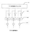
図2に上記のような、ゲイト信号線に高電圧の印加を必要とする液晶表示装置のゲイト信号線側駆動回路(ドライバ)の一例を示す。201はシフトレジスタ回路、202はインバータ、203はレベルシフタ、204は最終段のインバータである。最終段のインバータ204は、対応するゲイト信号線に接続されている。
【0023】
シフトレジスタ回路は、複数のフリップフロップ回路によって構成されている。シフトレジスタ回路に入力されるスタートパルス信号の入力により、シフトレジスタが所定のタイミングで動作を開始する。また、所定のクロック信号がシフトレジスタに入力される。このシフトレジスタ回路は、ゲイト信号線に対応した回路に動作タイミングを決定する信号を供給する機能を有している。
【0024】
シフトレジスタ201からの信号は、インバータ202へ出力される。インバータ202は、入力された上記信号を反転させ、レベルシフタ203へ出力する。
【0025】
レベルシフタ203の入力信号は、レベルシフタ203を通ることによって高電圧化され、ゲイト信号線に接続されている最終段のインバータ204へ出力される。その後、最終段のインバータ204によって反転した信号がゲイト信号線に出力される。
【0026】
この場合、ドライバの電源は2つ必要である。つまり、シフトレジスタ201、およびインバータ202には低電圧電源を、レベルシフタ203、および最終段のインバータ204には高電圧電源を用いてゲイト信号線へ高電圧の信号を供給している。
【0027】
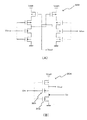
ここで、従来用いられているレベルシフタ203、およびインバータ204の回路の例を図3に示す。レベルシフタ203、およびインバータ204の電源電圧Vddhは16Vである。なお、図3(B)では、説明の便宜上、2つのNチャンネルTFTを区別するために、それぞれ符号301および302がつけられている。
【0028】
レベルシフタ203においては、Vinに入力された信号の高電圧化された反転信号が、Voutから出力されるように設計されている。レベルシフタ203のVoutから出力される信号は、最終段のインバータ204のVinに入力される。最終段のインバータ204に入力された信号は、反転され、Voutから対応するゲイト信号線に出力される。
【0029】
図4に、最終段のインバータ204の電圧変化をシミュレートした結果を示す。図4において、シンボル○は電源電圧Vddh(=16V)を、シンボル△は入力信号Vinを、シンボル▽は出力信号Voutを、シンボル□は、図3(B)に示すように、2つのNチャンネルTFTのソース・ドレイン間の電圧Vxを示す。なお、図4において、縦軸はVddh、Vout、およびVxの電圧値(V)を示し、横軸はVinの電圧値(V)を示す。
【0030】
また、図5に、最終段のインバータ204からゲイト信号線に出力される信号の波形を示す。図5において、縦軸は電圧値(V)、横軸は時間(μs)を示す。
【0031】
図4に示されるシミュレーション結果を検討すると、入力信号Vinが低いときには、VxがVoutに比較してかなり小さいことから、NチャンネルTFT301に電源電圧のほとんどの電圧がかかっており、NチャンネルTFT302には、わずかな電圧しかかかっていないことが理解される(図3)。
【0032】
よって、NチャンネルTFT301にかかる負荷が大きく、NチャンネルTFT301の劣化が生じてしまう。
【0033】
このことは、TFTに高電圧が印加された場合、ドレイン領域に発生する加速された高いエネルギーを持つホットキャリアによって、TFTのしきい値電圧などが変動し、経時変化が引き起こされることによる。
【0034】
ホットキャリアによるTFTの劣化は、ゲート・ソース間電圧が2V付近のときが最も大きいことが知られている。
【0035】
上述したようなNチャンネルTFT301の劣化によってゲイト信号線への信号の供給が絶たれ、結果として線欠陥などの表示欠陥が生じ、画質の低下を招くことになる。
【0036】
また、上記のようなアクティブマトリクス型の液晶表示装置には、一般的にTNモード(ツイストネマチックモード)による液晶の駆動がよく用いられている。TNモードによる液晶の駆動では、ネマチック液晶を90°捩じれた状態に配向させる。また、電圧を印加することによって捩じれ状態をとき、光学状態を変化させる。TN液晶内部では、直線偏光の偏光軸が回転するといった現象を利用して、一対の偏光板を通過する直線偏光によって所望の映像を得ることができる。
【0037】
TNモードでは、液晶を数ボルトといった低電圧で駆動することができ、数百万の画素一つ一つに対応するTFTを駆動する周辺駆動回路にかかる負担も比較的軽い。しかし、TNモードは、視野角が狭い、応答速度が遅いなどといった欠点を数多く有している。
【0038】
そこで、新しい液晶の駆動モードが研究されてきた。その中には、例えば、電界制御複屈折(ECB)モードやゲスト・ホストモードなどがある。これらのモードの中には、液晶にTNモードよりも高い電圧を印加することを必要とするモードもある。このような場合も、インバータ202からの出力をレベルシフタ203によって高電圧化し、最終段のインバータ204に出力する手段が採用されている。
【0039】
このように、液晶の駆動に高電圧を印加する場合も、上述したようなホットキャリアによるTFTの劣化の問題が生じてくる。
【0040】
そこで、本発明は、ゲイト信号線に高電圧を印加することを必要とし、周辺駆動回路の電源電圧を高電圧と低電圧との2つにした場合、高電圧側のCMOS回路のTFTの劣化を防ぎ、高耐圧化をはかり、駆動マージンの大きい駆動回路を提供することを目的とする。
【0041】
また、このような駆動回路を用いた液晶表示装置を提供することを目的とする。
【0042】
【課題を解決するための手段】
【0043】
本発明のある実施態様によると、
3つの電源Vdd1、Vdd2、およびVssと、
出力端子と、入力端子と、前記電源Vdd2と前記出力端子との間に接続される少なくとも1つのPチャンネル型TFTと、前記出力端子と前記Vssとの間に接続される2つのゲイト電極を有するNチャンネル型TFTと、から成る絶縁基板上に形成される複数のCMOS回路と、
を備えた表示装置の駆動回路であって、
前記Vdd2>前記Vdd1>前記Vssであり、前記Nチャンネル型TFTの前記2つのゲイト電極のうち、Pチャンネル型TFTに近い側のゲイト電極は前記Vdd1に接続されており、もう一方のゲイト電極は入力端子に接続されている駆動回路が提供される。このことによって上記目的が達成される。
【0044】
前記CMOS回路を有するレベルシフタおよびインバータあるいはバッファを含んでいてもよい。
【0045】
前記2つのゲイト電極を有するNチャンネル型TFTは、同一半導体層に形成されてもよい。
【0046】
前記Pチャンネル型TFTは、2つのゲイト電極を有していてもよい。
【0047】
また、本発明のある実施態様によると、
絶縁基板上に形成される、複数の画素TFTおよび前記画素TFTを駆動する駆動回路と、
前記複数の画素TFTによって光学応答が制御される表示媒体と、
を備える表示装置であって、
前記駆動回路は、3つの電源Vdd1、Vdd2、およびVssと、
出力端子と、入力端子と、前記電源Vdd2と前記出力端子との間に接続される少なくとも1つのPチャンネル型TFTと、前記出力端子と前記Vssとの間に接続される2つのゲイト電極を有するNチャンネル型TFTと、から成る絶縁基板上に形成される複数のCMOS回路と、を備えており、前記Vdd2>前記Vdd1>前記Vssであり、前記Nチャンネル型TFTの前記2つのゲイト電極のうち、Pチャンネル型TFTに近い側のゲイト電極は前記Vdd1に接続されており、もう一方のゲイト電極は入力端子に接続されている駆動回路を有する表示装置が提供される。このことによって上記目的が達成される。
【0048】
前記CMOS回路を有するレベルシフタおよびインバータを含んでいてもよい。
【0049】
前記2つのゲイト電極を有するNチャンネル型TFTは、同一半導体層に形成されてもよい。
【0050】
前記Pチャンネル型TFTは、2つのゲイト電極を有していてもよい。
【0051】
前記表示媒体は液晶であってもよい。
【0052】
前記液晶は反強誘電性液晶であってもよい。
【0053】
また、本発明のある実施態様によると、
2つの電源VddおよびVssと、
出力端子と、入力端子と、前記Vddと前記出力端子との間に接続される少なくとも1つのPチャネルエンハンスメント型TFTと、ソースあるいはドレインのいずれか一方が前記Vssに接続されるNチャンネルエンハンスメント型TFTと、前記Nチャンネルエンハンスメント型TFTのもう一方と前記出力端子との間に接続されるNチャンネルデプレッション型TFT、から成る絶縁基板上に形成された複数のCMOS回路を含む表示装置の駆動回路であって、
前記Vdd>前記Vssであり、前記Nチャンネルデプレッション型TFTのゲイト電極は、前記Nチャンネルデプレッション型TFTと前記Nチャンネルエンハンスメント型TFTとの接続部に接続されている表示装置の駆動回路が提供される。このことによって上記目的が達成される。
【0054】
前記CMOS回路を有するレベルシフタおよびインバータを含んでいてもよい。
【0055】
前記Nチャンネルエンハンスメント型TFTと前記Nチャンネルデプレッション型TFTとは、同一半導体層に形成されてもよい。
【0056】
前記Pチャンネルエンハンスメント型TFTと前記出力端子との間に、さらにPチャンネルエンハンスメント型TFTを含んでいてもよい。
【0057】
また、本発明のある実施態様によると、
絶縁基板上に形成される、複数の画素TFTと、
前記画素TFTを駆動する駆動回路と、
前記画素TFTによって光学応答が制御される液晶層と、
を備える表示装置であって、
前記駆動回路は、2つの電源VddおよびVssと、
出力端子と、入力端子と、前記Vddと前記出力端子との間に接続される少なくとも1つのPチャネルエンハンスメント型TFTと、ソースあるいはドレインのいずれか一方が前記Vssに接続されるNチャンネルエンハンスメント型TFTと、前記Nチャンネルエンハンスメント型TFTのもう一方と前記出力端子との間に接続されるNチャンネルデプレッション型TFT、から成る絶縁基板上に形成される複数のCMOS回路を含んでおり、
前記Vdd>前記Vssであり、前記Nチャンネルデプレッション型TFTのゲイト電極は、前記Nチャンネルデプレッション型TFTと前記Nチャンネルエンハンスメント型TFTとの接続部に接続されている表示装置が提供される。このことによって上記目的が達成される。
【0058】
前記CMOS回路を有するレベルシフタおよびインバータを含んでいてもよい。
【0059】
前記少なくとも1個のNチャンネル型TFTと前記Nチャンネルデプレッション型TFTとは、同一半導体層に形成されていてもよい。
【0060】
前記Pチャンネルエンハンスメント型TFTと前記出力端子との間に、さらにPチャンネルエンハンスメント型TFTを含んでいてもよい。
【0061】
また、本発明のある実施態様によると、
3つの電源Vdd1、Vdd2、およびVssと、
低電源電圧駆動部と、
高電源電圧駆動部と、
を含む表示装置の駆動回路であって、
前記Vdd2>前記Vdd1>前記Vssであり、
前記高電源電圧駆動部は、出力端子と、入力端子と、前記電源Vdd2と前記出力端子との間に接続される少なくとも1つのPチャンネル型TFTと、前記出力端子と前記Vssとの間に接続される2つのゲイト電極を有するNチャンネル型TFTと、から成る絶縁基板上に形成される複数のCMOS回路と、を備えており、
前記Nチャンネル型TFTの前記2つのゲイト電極のうち、Pチャンネル型TFTに近い側のゲイト電極は前記Vdd1に接続されており、もう一方のゲイト電極は入力端子に接続されており、
前記低電源電圧駆動部の電源には、前記Vdd1が印加される表示装置の駆動回路が提供される。このことによって上記目的が達成される。
【0062】
【発明の実施の形態】
【0063】
【実施例】
【0064】
本発明の液晶表示装置は、そのゲイト信号線側のドライバ回路には、低電源電圧駆動部と高電源電圧駆動部とを有している。本発明によると、高電源電圧駆動部の回路の高耐圧化を実現できる。
【0065】
(実施例1)
【0066】
本実施例では、高耐圧化を実現できるゲイト信号線側のドライバ回路について、シミュレーション結果をもとに説明する。
【0067】
図6に上記のような、ゲイト信号線に高電圧の印加を必要とする液晶表示装置のゲイト信号線側駆動回路(ドライバ)の一例を示す。601はシフトレジスタ回路、602はインバータ、603はレベルシフタ、604は最終段のインバータである。最終段のインバータ604は、対応するゲイト信号線に接続されている。なお、アナログバッファ回路、アナログスイッチ回路、あるいはその他の回路が必要に応じて用いられる。また、本実施例では、便宜上、シフトレジスタ回路は3つのフリップフロップ回路のみによって示されているが、画素の数に応じて適時その数が変更される。また、本実施例の駆動回路には、3つの電源Vdd1、Vdd2、GND(Vdd2>Vdd1>GND)が使用されている。シフトレジスタ601からインバータ602までの回路の電源には、Vdd1が用いられており、この部分を低電源電圧駆動部と呼ぶ。また、レベルシフタ603から最終段のインバータまでの回路の電源には、Vdd2が用いられており、この部分を高電源電圧駆動部と呼ぶ。
【0068】
シフトレジスタ回路601は、複数のフリップフロップ回路によって構成されている。シフトレジスタ回路601に入力されるSPは、スタートパルスの略であり、このスタートパルス信号の入力により、シフトレジスタが所定のタイミングで動作を開始する。また、シフトレジスタ回路601に入力されるCLKは、クロック信号の略であり、所定のクロック信号がシフトレジスタに入力される。このシフトレジスタ回路は、ゲイト信号線に対応した回路に動作タイミングを決定する信号を供給する機能を有している。
【0069】
シフトレジスタ601からの信号は、インバータ602へ出力される。インバータ602は、入力された上記信号を反転させ、レベルシフタ603へ出力する。
【0070】
レベルシフタ603は、2つの入力VinおよびVinbを有しており、本実施例では、シフトレジスタ回路601からの信号がVinに入力され、その反転信号がVinbに入力される。
【0071】
レベルシフタ603の入力信号は、レベルシフタ603を通ることによって高電圧化され、ゲイト信号線に接続されている最終段のインバータ604へ出力される。その後、最終段のインバータ604によって反転した信号がゲイト信号線に出力される。
【0072】
図7に本実施例のゲイト信号線側の高電圧側のドライバ回路を示す。図7(A)は、レベルシフタ603の回路を、図7(B)は、ゲイト信号線に接続される最終段のインバータ604の回路を示す。図7(A)および(B)においては、それぞれのTFTにTr1〜Tr11の符号が付けられている。
【0073】
なお、本実施例では、レベルシフタ回路および最終段のインバータ回路のみについて説明するが、必要に応じて、シフトレジスタ回路、アナログバッファ回路などがゲイト信号線側ドライバに用いられる。
【0074】
図7(A)を参照する。本実施例のレベルシフタ603は、8個のエンハンスメント型のTFTから構成されており、電源電圧Vdd2(高電圧電源)が印加されている。また、レベルシフタ603の2つのNチャンネルTFTTr3およびTr7には、上記電源電圧とは異なる電源電圧であるバイアス電圧Vdd1(低電圧電源)が印加されている。また、Tr4およびTr8はGNDに接続されている。なお、本実施例では、Vdd1=10V、Vdd2=16Vである。
【0075】
VinにHiの信号が入力されるときは、Vinbにその反転信号Loが入力される。なお、レベルシフタ603のVinにHiの信号が入力されたときは、信号の出力端に接続された出力端子VoutからはLoの信号が出力される。また、レベルシフタ603のVinにLoの信号が入力されたときは、出力Voutからは電圧レベルが16VにシフトされたHiの信号が出力される。つまり、レベルシフタ603では、Vinに入力された信号のレベルは反転されかつ高電位にシフトし、最終段のインバータ604へ送出される。
【0076】
図7(B)には、ゲイト信号線に接続される最終段のインバータ604の回路が示される。インバータ604は、シングルゲイトのPチャネルエンハンスメント型TFTTr9とダブルゲイトのNチャネルエンハンスメント型TFTTr10およびTr11とから成るCMOS回路によって構成されている。なお、Tr10およびTr11は、同一の半導体活性層によって形成される。つまり、Tr10およびTr11は、同一の半導体活性層上に2つのゲイト電極が形成されることによって構成される。
【0077】
また、インバータ604にも電源電圧Vdd2(高電圧電源)が印加されており、NチャンネルTFTTr10には、前記電源電圧とは異なる電源電圧であるバイアス電圧Vdd1(低電圧電源)が印加されている。また、Tr12はGNDに接続されている。なお本実施では、上記レベルシフタ603と同じように、Vdd1=10V、Vdd2=16Vである。
【0078】
図7(A)に示されるレベルシフタ603からの出力信号Voutが、図7(B)に示されるインバータ回路の入力端子Vinに入力され、その反転信号が信号の出力端に接続された出力端子Voutから出力され、ゲイト信号線に出力される。
【0079】
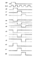
ここで、シフトレジスタ回路601、インバータ602、レベルシフタ603、および最終段のインバータ604の動作を、図8に示されるタイミングチャートを用いて説明する。
【0080】
シフトレジスタ回路601から送出される信号をa0〜a2とし、インバータ602から送出される信号をb0〜b2とし、レベルシフタ603から送出される信号をc0〜c2とし、最終段のインバータ604から対応するゲイト信号線に送出される信号をd0〜d2とする。
【0081】
シフトレジスタ回路601から送出される信号a0は分岐され、一方はレベルシフタ603のVinへ入力され、もう一方はインバータ602によって反転され(b0)、レベルシフタ603のVinbに入力される。その後、レベルシフタ603からレベルが高電位にシフトされたc0が出力される。次に、出力c0は最終段のインバータ604に入力され、その反転信号d0が対応するゲイト信号線に出力される。よって、レベルシフタ603は、ゲイト信号線に信号を供給するタイミングで負の信号が出力されるように設計されている。
【0082】
このゲイト信号線に送出される信号と、ソース側のドライバによって供給される信号(図示せず)とによって画素TFTがスイッチングされ、所望の画素を点灯あるいは消灯させることができる。
【0083】
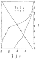
ここで、図9に本実施例のインバータの電圧変化のシミュレーション結果を示す。図9において、シンボル○は電源電圧Vdd2(=16V)を、シンボル△は入力信号Vinを、シンボル▽は出力信号Voutを、シンボル□は、図7(B)に示される2つのNチャンネルTFTTr10およびTr11のソース・ドレイン間の電圧Vxを示す。なお、図9において、縦軸はVdd2、VoutおよびVxの電圧値を示し、横軸はVinの電圧値を示す。
【0084】
このシミュレーション結果を検討すると、入力Vinの大きさにかかわらず、2つのNチャネル型TFTTr10とTr11とのソース・ドレイン間の電圧Vxが、出力Voutのほぼ半分の値をとることがわかる。言い換えると、2つのNチャンネルTFTTr10とTr11とには、ほぼ均一に電圧がかかることが分かる。従って、電源電圧が16Vと比較的高い場合にも、2つのNチャンネルTFTTr10およびTr11には、ほぼ均等に負荷がかかり、一方のTFTのみに高負荷がかかることはない。
【0085】
ここで、図10に、本実施例の最終段のインバータ604からのゲイト信号線への出力Voutの波形を示す。図10において、シンボル○は出力Voutを、シンボル□は入力Vinを示している。また、図10において、縦軸は電圧(V)、横軸は時間(μs)を示す。
【0086】
ここで、図10と、図5に示した従来の最終段のインバータからのゲイト信号線への出力波形とを比較すると、本実施例のインバータからの出力のほうがやや立ち下がりが遅くなる傾向がみられる。これは、図7(B)のTr10のゲイト電圧に制限があるためと考えられる。しかし、このことはTFTのサイズを最適化することによって解決できると考えられ、あまり問題ではない。
【0087】
また、レベルシフタのシミュレーション結果は、本実施例の説明においては特に用いなかったが、2つのNチャンネルTFTTr3およびTr7にはバイアス電圧Vdd1が印加されているので、本実施例の最終段のインバータ604と同様の効果が得られることは言うまでもない。
【0088】
以上のことから、本実施例のレベルシフタ603および最終段のインバータ604を用いると、レベルシフタ603および最終段のインバータ604を構成するTFTの電圧マージンを高くすることができる。よって、ゲイト信号線の駆動に高電圧の印加が必要な場合にも、ホットキャリアによって、TFTのしきい値電圧などが変動する経時変化が引き起こされることを防ぐことができる。結果として、ゲイト信号線の欠陥による線欠陥などを防ぐことができ、画質の低下を防ぐことができる。
【0089】
なお、本実施例では、レベルシフタ603と最終段のインバータ604との間に、更なるインバータあるいはバッファを複数追加してもよい。この場合追加されるインバータあるいはバッファを構成するCMOS回路のNチャンネルTFTの一つには、本実施例の最終段のインバータ604のように、バイアス電圧が印加される。
【0090】
また、本実施例の駆動回路は、ゲイト信号線の駆動に高電圧を要する場合でも、低電圧で駆動する回路と高電圧で駆動する回路とに分けており、全ての回路を高電圧で駆動する必要がないので、低消費電力化がはかれる。
【0091】
(実施例2)
【0092】
本実施例では、ゲイト信号線側ドライバの高電源電圧駆動部のレベルシフタと最終段のインバータとを構成する回路の一例を示す。
【0093】
図11を参照する。図11(A)には、Tr1〜Tr12の12個のTFTを用いて構成されるレベルシフタと最終段のインバータとの回路が示される。
【0094】
図11(A)において、1101〜1106は半導体層であり、エンハンスメント型TFTTr1〜Tr12を構成している。1107は第1の配線層であり、TFTのゲイト電極や出力用の引き出し配線として利用している。また、1108は第2の配線層であり、入力端子(VinおよびVinb)と、電源端子(Vdd1、Vdd2、およびVss端子)と、TFTとを接続している。また、図中において、1109で示したように黒く塗りつぶされている部分は、その下部の配線あるいは半導体層とコンタクトをとっていることを示している。なお、図中において同一柄の配線は全て同一の配線層である。なお、出力端子Voutはゲイト信号線に接続されている。
【0095】
なお、本実施例においては、Tr1〜Tr12のチャネル長(L)とチャネル幅(W)は以下のように設計された。
Tr1、Tr2、Tr5、Tr6;L=4μm、W=60μm
Tr3、Tr4、Tr7、Tr8;L=4μm、W=40μm
Tr9、Tr10 ;L=4μm、W=120μm
Tr11、Tr12 ;L=4μm、W=80μm
【0096】
また、図11(B)には、図11(A)の等価回路が示される。
【0097】
なお、本実施例では、電源としてVdd1、Vdd2、およびVssを用い、Vdd2−Vss=16V、Vdd1−Vss=10Vとした。
【0098】
本実施例のレベルシフタは、VinおよびVinbの2つの入力に信号が入力される。
本実施例のレベルシフタにおいては、VinがHiのとき、最終段のインバータにLoが送出され、VinがLoのとき最終段のインバータにHiが送出されるように設計されている。
【0099】
本実施例のような構成を有するゲイト信号線の駆動回路では、レベルシフタおよびゲイト信号線に接続されている最終段のインバータのCMOS回路において、Pチャンネル型TFTに近い方のNチャンネル型TFTにバイアス電圧が印加されている。よって、実施例1で示したように、レベルシフタおよび最終段のインバータを構成するTFTの電圧マージンを高くすることができる。
【0100】
また、ゲイト信号線の駆動に高電圧の印加が必要な場合にも、ホットキャリアによって、TFTのしきい値電圧などが変動する経時変化を引き起こすことを防ぐことができる。結果として、ゲイト信号線の欠陥による線欠陥などを防ぐことができ、画質の低下を防ぐことができる。
【0101】
(実施例3)
【0102】
本実施例では、実施例1あるいは2で用いたドライバ回路を有する液晶表示装置の作製工程について説明する。
【0103】
本実施例では絶縁表面を有する基板上に複数のTFTを形成し、画素マトリクス回路とドライバ回路を含む周辺回路とをモノリシックに構成する例を図12〜図16に示す。なお、本実施例ではドライバ回路やロジック回路等の周辺回路の例として、基本回路であるCMOS回路を示す。なお、本実施例では、Pチャンネル型とNチャンネル型とがそれぞれ1つのゲイト電極を備えたCMOS回路について、その作製工程を説明するが、ダブルゲイト型のような複数のゲイト電極を備えたCMOS回路も同様に作製することができる。
【0104】
図12を参照する。まず、絶縁表面を有する基板として石英基板1201を準備する。石英基板の代わりに熱酸化膜を形成したシリコン基板を用いることもできる。また、石英基板上に一旦非晶質珪素膜を形成し、それを完全に熱酸化して絶縁膜とする様な方法をとっても良い。さらに、絶縁膜として窒化珪素膜を形成した石英基板、セラミックス基板またはシリコン基板を用いても良い。
【0105】
1202は非晶質珪素膜であり、最終的な膜厚(熱酸化後の膜減りを考慮した膜厚)が10〜75nm(好ましくは15〜45nm)となる様に調節する。なお、成膜に際して膜中の不純物濃度の管理を徹底的に行うことは重要である。
【0106】
本実施例の場合、非晶質珪素膜1202中において代表的な不純物であるC(炭素)、N(窒素)、O(酸素)、S(硫黄)の濃度はいずれも5×10 18 atoms/cm 3 未満(好ましくは1×10 18 atoms/cm 3 以下)となる様に管理している。各不純物がこれ以上の濃度で存在すると、結晶化の際に悪影響を及ぼし、結晶化後の膜質を低下させる原因となりうる。
【0107】
なお、非晶質珪素膜1202中の水素濃度も非常に重要なパラメータであり、水素含有量を低く抑えた方が結晶性の良い膜が得られる様である。そのため、非晶質珪素膜1202の成膜は減圧熱CVD法であることが好ましい。なお、成膜条件を最適化することでプラズマCVD法を用いることも可能である。
【0108】
次に、非晶質珪素膜1202の結晶化工程を行う。結晶化の手段としては特開平7−130652号公報記載の技術を用いる。同公報の実施例1および実施例2のどちらの手段でも良いが、本実施例では、同公報の実施例2に記載した技術内容(特開平8−78329号公報に詳しい)を利用するのが好ましい。
【0109】
特開平8−78329号公報記載の技術は、まず触媒元素の添加領域を選択するマスク絶縁膜1203を形成する。マスク絶縁膜1203は触媒元素を添加するために複数箇所の開口部を有している。この開口部の位置によって結晶領域の位置を決定することができる。
【0110】
そして、非晶質珪素膜の結晶化を助長する触媒元素としてニッケル(Ni)を含有した溶液をスピンコート法により塗布し、Ni含有層1204を形成する。なお、触媒元素としてはニッケル以外にも、コバルト(Co)、鉄(Fe)、パラジウム(Pd)、白金(Pt)、銅(Cu)、金(Au)等を用いることができる(図12(A))。
【0111】
また、上記触媒元素の添加工程は、レジストマスクを利用したイオン注入法またはプラズマドーピング法を用いることもできる。この場合、添加領域の占有面積の低減、横成長領域の成長距離の制御が容易となるので、微細化した回路を構成する際に有効な技術となる。
【0112】
次に、触媒元素の添加工程が終了したら、450℃で1時間程度の水素出しの後、不活性雰囲気、水素雰囲気または酸素雰囲気中において500〜700℃(代表的には550〜650℃)の温度で4〜24時間の加熱処理を加えて非晶質珪素膜1202の結晶化を行う。本実施例では窒素雰囲気で570℃で14時間の加熱処理を行う。
【0113】
この時、非晶質珪素膜1202の結晶化はニッケルを添加した領域1205および1206で発生した核から優先的に進行し、基板1201の基板面に対してほぼ平行に成長した結晶領域1207および1208が形成される。この結晶領域1207および1208を横成長領域と呼ぶ。横成長領域は比較的揃った状態で個々の結晶が集合しているため、全体的な結晶性に優れるという利点がある(図12(B))。
【0114】
なお、上述の特開平7−130652号公報の実施例1に記載された技術を用いた場合も微視的には横成長領域と呼びうる領域が形成されている。しかしながら、核発生が面内において不均一に起こるので結晶粒界の制御性の面で難がある。
【0115】
結晶化のための加熱処理が終了したら、マスク絶縁膜1203を除去してパターニングを行い、横成長領域1207および1208でなる島状半導体層(活性層)1209、1210、および1211を形成する(図12(C))。
【0116】
ここで1209はCMOS回路を構成するN型TFTの活性層、1210はCMOS回路を構成するP型TFTの活性層、1211は画素マトリクス回路を構成するN型TFT(画素TFT)の活性層である。
【0117】
活性層1209、1210、および1211を形成したら、その上に珪素を含む絶縁膜でなるゲイト絶縁膜1212を成膜する。
【0118】
そして、次に図12(D)に示す様に触媒元素(ニッケル)を除去または低減するための加熱処理(触媒元素のゲッタリングプロセス)を行う。この加熱処理は処理雰囲気中にハロゲン元素を含ませ、ハロゲン元素による金属元素のゲッタリング効果を利用するものである。
【0119】
なお、ハロゲン元素によるゲッタリング効果を十分に得るためには、上記加熱処理を700℃を超える温度で行なうことが好ましい。この温度以下では処理雰囲気中のハロゲン化合物の分解が困難となり、ゲッタリング効果が得られなくなる恐れがある。
【0120】
そのため本実施例ではこの加熱処理を700℃を超える温度で行い、好ましくは800〜1000℃(代表的には950℃)とし、処理時間は0.1〜6hr、代表的には0.5〜1hrとする。
【0121】
なお、本実施例では酸素雰囲気中に対して塩化水素(HCl)を0.5〜10体積%(本実施例では3体積%)の濃度で含有させた雰囲気中において、950℃で、30分の加熱処理を行う例を示す。HCl濃度を上記濃度以上とすると、活性層1209、1210、および1211の表面に膜厚程度の凹凸が生じてしまうため好ましくない。
【0122】
また、ハロゲン元素を含む化合物してHClガスを用いる例を示したが、それ以外のガスとして、代表的にはHF、NF 3 、HBr、Cl 2 、ClF 3 、BCl 3 、F 2 、Br 2 等のハロゲンを含む化合物から選ばれた一種または複数種のものを用いることが出来る。
【0123】
この工程においては活性層1209、1210、および1211中のニッケルが塩素の作用によりゲッタリングされ、揮発性の塩化ニッケルとなって大気中へ離脱して除去されると考えられる。そして、この工程により活性層1209、1210、および1211中のニッケルの濃度は5×10¹⁷atoms/cm3以下にまで低減される。
【0124】
なお、5×10¹⁷atoms/cm3という値はSIMS(質量二次イオン分析)の検出下限である。本発明者らが試作したTFTを解析した結果、1×10 18 atoms/cm 3 以下(好ましくは 5×10¹⁷atoms/cm3以下)ではTFT特性に対するニッケルの影響は確認されなかった。ただし、本明細書中における不純物濃度は、SIMS分析の測定結果の最小値でもって定義される。
【0125】
また、上記加熱処理により活性層1209、1210、および1211とゲイト絶縁膜1212の界面では熱酸化反応が進行し、熱酸化膜の分だけゲイト絶縁膜1212の膜厚は増加する。この様にして熱酸化膜を形成すると、非常に界面準位の少ない半導体/絶縁膜界面を得ることができる。また、活性層端部における熱酸化膜の形成不良(エッジシニング)を防ぐ効果もある。
【0126】
さらに、上記ハロゲン雰囲気における加熱処理を施した後に、窒素雰囲気中で950℃で1時間程度の加熱処理を行なうことで、ゲイト絶縁膜1212の膜質の向上を図ることも有効である。
【0127】
なお、SIMS分析により活性層1209、1210、および1211中にはゲッタリング処理に使用したハロゲン元素が、1×10¹⁵atoms/cm3〜1×1020atoms/cm3の濃度で残存することも確認されている。また、その際、活性層1209、1210、および1211と加熱処理によって形成される熱酸化膜との間に前述のハロゲン元素が高濃度に分布することがSIMS分析によって確かめられている。
【0128】
また、他の元素についてもSIMS分析を行った結果、代表的な不純物であるC(炭素)、N(窒素)、O(酸素)、S(硫黄)はいずれも5×10¹⁸atoms/cm3未満(典型的には1×1018atoms/cm3以下)であることが確認された。
【0129】
次に、図示しないアルミニウムを主成分とする金属膜を成膜し、パターニングによって後のゲイト電極の原型1213、1214、および1215を形成する。本実施例では2wt%のスカンジウムを含有したアルミニウム膜を用いる(図13(A))。
【0130】
次に、特開平7−135318号公報記載の技術により多孔性の陽極酸化膜1216、1217、および1218、無孔性の陽極酸化膜1219、1220、および1221、ゲイト電極1222、1223、および1224を形成する(図13(B))。
【0131】
こうして図13(B)の状態が得られたら、次にゲイト電極1222、1223、および1224、多孔性の陽極酸化膜1216、1217、および1218をマスクとしてゲイト絶縁膜1212をエッチングする。そして、多孔性の陽極酸化膜1216、1217、および1218を除去して図13(C)の状態を得る。なお、図13(C)において1225、1226、および1227で示されるのは加工後のゲイト絶縁膜である。
【0132】
次に、一導電性を付与する不純物元素の添加工程を行う。不純物元素としてはN型ならばP(リン)またはAs(砒素)、P型ならばB(ボロン)を用いれば良い。
【0133】
本実施例では、不純物添加を2回の工程に分けて行う。まず、1回目の不純物添加(本実施例ではP(リン)を用いる)を高加速電圧80keV程度で行い、n − 領域を形成する。このn − 領域は、Pイオン濃度が1×10¹⁸atoms/cm3〜1×1019atoms/cm3となるように調節する。
【0134】
さらに、2回目の不純物添加を低加速電圧10keV程度で行い、n + 領域を形成する。この時は、加速電圧が低いので、ゲイト絶縁膜がマスクとして機能する。また、このn+領域は、シート抵抗が500Ω以下(好ましくは300Ω以下)となるように調節する。
【0135】
以上の工程を経て、CMOS回路を構成するN型TFTのソース領域1228、ドレイン領域1229、低濃度不純物領域1230、チャネル形成領域1231が形成される。また、画素TFTを構成するN型TFTのソース領域1232、ドレイン領域1233、低濃度不純物領域1234、チャネル形成領域1235が確定する(図13(D))。
【0136】
なお、図13(D)に示す状態ではCMOS回路を構成するP型TFTの活性層もN型TFTの活性層と同じ構成となっている。
【0137】
次に、図14(A)に示すように、N型TFTを覆ってレジストマスク1236を設け、P型を付与する不純物イオン(本実施例ではボロンを用いる)の添加を行う。
【0138】
この工程も前述の不純物添加工程と同様に2回に分けて行うが、N型をP型に反転させる必要があるため、前述のPイオンの添加濃度の数倍程度の濃度のB(ボロン)イオンを添加する。
【0139】
こうしてCMOS回路を構成するP型TFTのソース領域1237、ドレイン領域1238、低濃度不純物領域1239、チャネル形成領域1240が形成される(図14(A))。
【0139】
以上の様にして活性層が完成したら、ファーネスアニール、レーザーアニール、ランプアニール等の組み合わせによって不純物イオンの活性化を行う。それと同時に添加工程で受けた活性層の損傷も修復される。
【0140】
次に、層間絶縁膜1241として酸化珪素膜と窒化珪素膜との積層膜を形成し、コンタクトホールを形成した後、ソース電極1242、1243、および1244、ドレイン電極1245、1246を形成して図14(B)に示す状態を得る。
【0141】
次に、10〜50nmの厚さの窒化珪素膜1247、ブラックマスク1248を形成する(図14(C))。
【0142】
図14(C)の構成では、窒化珪素膜1247を介して、ドレイン電極1246とブラックマスク1248との間で補助容量を形成する。
【0143】
このように、図14(C)の構成では、ブラックマスク1248が補助容量の上部電極を兼ねる点が特徴である。
【0144】
なお、図14(C)に示すような構成では、広い面積を占めやすい補助容量をTFTの上に形成することで開口率の低下を防ぐことが可能である。また、誘電率の高い窒化珪素膜を25nm程度の厚さで利用できるので、少ない面積で非常に大きな容量を確保することが可能である。
【0145】
次に、有機性樹脂膜でなる第2の層間絶縁膜1249を0.5〜3μmの厚さに形成する。そして、層間絶縁膜1249上に導電膜を形成しパターニングすることにより画素電極1250を形成する。本実施例は透過型の例であるため画素電極1250を構成する導電膜としてITO等の透明導電膜を用いる。
【0146】
次に、基板全体を350℃の水素雰囲気で1〜2時間加熱し、素子全体の水素化を行うことで膜中(特に活性層中)のダングリングボンド(不対結合手)を補償する。以上の工程を経て同一基板上にCMOS回路および画素マトリクス回路を作製することができる。
【0147】
次に、図15に示すように、上記の工程によって作製されたアクティブマトリクス基板をもとに、液晶パネルを作製する工程を説明する。
【0148】
図14(C)の状態のアクティブマトリクス基板に配向膜1251を形成する。本実施例では、配向膜1251には、ポリイミドを用いた。次に、対向基板を用意する。対向基板は、ガラス基板1252、透明導電膜1253、配向膜1254とで構成される。
【0149】
なお、本実施例では、配向膜には、液晶分子が基板に対して垂直に配向するようなポリイミド膜を用いた。なお、配向膜形成後、ラビング処理を施すことにより、液晶分子がある一定のプレチルト角を持って垂直配向するようにした。
【0150】
なお、対向基板には必要に応じてブラックマスクやカラーフィルタなどが形成されるが、ここでは省略する。
【0151】
次に、上記の工程を経たアクティブマトリクス基板と対向基板とを公知のセル組み工程によって、シール材やスペーサ(図示せず)などを介して貼り合わせる。その後、両基板の間に液晶材料1255を注入し、封止剤(図示せず)によって完全に封止する。よって、図15に示すような透過型の液晶パネルが完成する。
【0152】
なお、本実施例では、液晶パネルが、ECB(電界制御複屈折)モードによって表示を行うようにした。そのため、1対の偏光板(図示せず)がクロスニコル(1対の偏光板が、それぞれの偏光軸を直交させるような状態)で、液晶パネルを挟持するように配置された。
【0153】
よって、本実施例では、液晶パネルに電圧が印加されていないとき黒表示となる、ノーマリブラックモードで表示を行うことが理解される。
【0154】
また、図14(C)に示した様なアクティブマトリクス基板の外観を図16に簡略化して示す。図16において、1601は石英基板、1602は画素マトリクス回路、1603はソースドライバ回路、1604はゲイトドライバ回路、1605はロジック回路である。
【0155】
図16において、ゲイトドライバ回路1604に形成される、本発明のレベルシフタ、およびゲイト信号線に接続される最終段のインバータを構成するCMOS回路の一方のNチャンネルTFTには、実施例1あるいは2で説明されたようにバイアス電圧が印加されている。よって、ゲイトドライバ回路の高耐圧化がはかられている。
【0156】
ロジック回路1605は広義的にはTFTで構成される論理回路全てを含むが、ここでは従来から画素マトリクス回路、ドライバ回路と呼ばれている回路と区別するため、それ以外の信号処理回路(メモリ、D/Aコンバータ、パルスジェネレータ等)を指す。
【0157】
また、こうして形成された液晶パネルには外部端子としてFPC(Flexible Print Circuit)端子が取り付けられる。一般的に液晶モジュールと呼ばれるのはFPCを取り付けた状態の液晶パネルである。
【0158】
また、本実施例の液晶パネルは、本発明のレベルシフタおよび最終段のインバータをゲイト信号線の駆動回路に用いており、プロジェクタ用の2インチ程度の液晶パネルから、十数インチ程度の大画面の液晶パネルまであらゆるサイズの液晶パネルが実現できる。
【0159】
(実施例4)
【0160】
図17を参照する。本実施例のゲイト信号線側ドライバの高電源電圧駆動部のレベルシフタ1701、およびゲイト信号線に接続される最終段のインバータ1702には、レベルシフタ以前の低電源電圧駆動部(シフトレジスタ回路、インバータなど)よりも高い電源電圧が印加される。
【0161】
本実施例のレベルシフタ1701において、Tr3およびTr7はデプレッション型TFTであり、他のTrは、エンハンスメント型TFTである(図17(A))。図17(A)および(B)においては、それぞれのTFTにTr1〜Tr11の符号が付けられている。
【0162】
また、本実施例のインバータ1702において、Tr10はデプレッション型TFTであり、Tr9およびTr11はエンハンスメント型TFTである。
【0163】
なお、本実施例では、レベルシフタ回路および最終段のインバータ回路のみについて説明するが、必要に応じて、シフトレジスタ回路、アナログバッファ回路などがゲイト信号線側ドライバに用いられる。
【0164】
図17(A)を参照する。本実施例のレベルシフタ1701は2つのCMOS回路から構成されており、電源電圧Vddが印加されている。Tr4およびTr8はGNDに接続されている。また、Tr3およびTr4のソース・ドレイン間の電圧がTr3のゲイト電極に印加されるように設計されている。また、同様に、Tr7およびTr8のソース・ドレイン間の電圧がTr7のゲイト電極に印加されるように設計されている。よって、Tr3とTr4とに印加される電位は、ほぼ半分になる。また、Tr7とTr8とに印加される電位は分配される。よって、一方のTFTのみに高負荷がかかることはなく、TFTの高耐圧化をはかることができる。
【0165】
シフトレジスタ回路(図示せず)からのレベルシフタ1701への入力信号は、VinにHiの信号が入力されるときは、Vinbにその反転信号Loが入力される。なお、レベルシフタ1701のVinにHiの信号が入力されたときは、出力VoutからはLoの信号が出力される。また、レベルシフタ1701のVinにLoの信号が入力されたときは、出力Voutからは電圧レベルが16VにシフトされたHiの信号が出力される。つまり、このレベルシフタ回路では、Vinに入力された信号のレベルは反転されかつ高電位にシフトし、最終段のインバータ1702へ送出される。
【0166】
図17(B)には、ゲイト信号線に接続される最終段のインバータ1702の回路が示される。インバータ1702は、シングルゲイトのPチャネル型TFTTr9とダブルゲイトのNチャネル型TFTTr10およびTr11とから成るCMOS回路によって構成されている。なお、Tr10およびTr11は、同一の半導体活性層によって形成される。つまり、Tr10およびTr11は、同一の半導体活性層上に2つのゲイト電極が形成されることによって構成される。
【0167】
また、インバータ1702にも電源電圧Vddが印加されており、NチャンネルTFTTr10には、Tr10およびTr11のソース・ドレイン間の電位がTr10のゲイト電極に印加されるように設計されている。よって、Tr10とTr11とに印加される電位は分配される。よって、一方のTFTのみに高負荷がかかることはない。
【0168】
図17(A)に示されるレベルシフタ1701からの出力信号Voutが、図17(B)に示されるインバータ1702のVinに入力され、その反転信号がVoutから出力され、ゲイト信号線に出力される。
【0169】
本実施例のレベルシフタ1701およびインバータ1702は、Tr3、Tr7、Tr10にデプレッション型のTFTを用いており、実施例3で説明したCMOS回路の作製工程において、イオンドーピングの工程を変化させることによって作製され得る。
【0170】
また、本実施例のレベルシフタ1701およびインバータ1702は、Tr3、Tr7、Tr10のゲイト電極には、電源電圧よりも低い電圧が印加されるように設計されている。よって、TFTの高耐圧化がはかれる。
【0171】
(実施例5)
【0172】
本実施例では、上記実施例1、2、あるいは4に示したような、本発明のドライバを含む周辺回路一体型の液晶パネルを組み込んだ3板式のプロジェクタについて説明する。
【0173】
図18を参照する。図18に、本実施例3の液晶パネルを用いた3板式の液晶プロジェクタを示す。1801は光源であり、1802、1803は、それぞれR(赤)とG(緑)との波長領域の光を選択的に反射するダイクロイックミラーである。1804、1805、および1806は、全反射ミラーであり、1807、1808、および1809は、それぞれR、G、Bに対応した透過型液晶パネルである。1810はダイクロイックプリズムであり、1811は投射レンズであり、1812はスクリーンである。
【0174】
本実施例の3板式の液晶プロジェクタは、3枚の白黒表示の液晶パネル1807、1808、および1809にそれぞれ赤、青、緑の3原色に対応した画像を表示し、それに対応する3原色の光で上記液晶パネルを照明する。そして、得られた各原色成分の画像をダイクロイックプリズム1810により合成してスクリーン1812に投射する。従って、3板式の液晶プロジェクタは、表示性能(解像度、スクリーン照度、色純度)に優れている。
【0175】
(実施例6)
【0176】
本実施例では、上記実施例1、2、あるいは4に示したような、本発明のドライバを含む周辺回路一体型の液晶パネルを組み込んだ単板式のプロジェクタについて説明する。
【0177】
本実施例の単板式の液晶プロジェクタの構成を図19に示す。1901は光源、1902は集光レンズ、1903は液晶パネル、1904は投射レンズ、1905はスクリーンである。なお、液晶パネル1903にはカラーフィルタが取り付けられている。
【0178】
なお、本実施例の単板式の液晶プロジェクタでは、カラーフィルタを用いて直視型の液晶表示装置と同じ方式によって、R、G、Bの各画素をそれぞれ駆動する方法で、得られた各画素に対応する光をスクリーンへ投射している。
【0179】
なお、単板式の液晶プロジェクタは、実施例5の3板式の液晶プロジェクタと比較して、光学部品が1/3で済むことから、価格やサイズなどにおいて優れている。しかし、3板式と従来の単板式とで同じ液晶パネルを用いた場合、3板式は1つの画素に3色を重ねているのに対して、単板式は1つの画素を一色の画素としてしか利用できないため、単板式は3板式に比べて画質が劣る。しかも、上記の単板式の液晶プロジェクタは、光源からの白色光のうち不要な成分をカラーフィルタに吸収させることによって所望の色の画像を得ている。よって、液晶パネルに入射した白色光は、1/3しか透過せず、光の利用効率が比較的低い。
【0180】
よって、実施例5の3板式のプロジェクタと本実施例の単板式のプロジェクタとがその用途に応じて使用され得る。
【0181】
(実施例7)
【0182】
本実施例では、実施例5あるいは実施例6に示された液晶プロジェクタを、光学エンジンとしてセットに組み込んだプロジェクタ(プロジェクションTV)について説明する。
【0183】
図20に、本実施例のプロジェクションTVの外観図を示す。本実施例のプロジェクションTVは、一般的に、リア型プロジェクタとも呼ばれるタイプである
。なお、図20(A)は側面図であり、内部構造を簡略化して示されている。また、図20(B)は、本実施例のプロジェクションTVを斜めから見た図である。
【0184】
図20(A)および(B)において、2001は本体、2002は実施例4あるいは実施例5の液晶プロジェクタが組み込まれた光学エンジン、2003はリフレクター、2004はスクリーンである。実際には、その他の光学系が加わって複雑な構成となるが、本実施例では概略の構成のみを示すこととする。
【0185】
なお、実施例5あるいは実施例6の液晶パネルには、周辺駆動回路および論理回路とが画素領域とともに一体形成されている。よって、NTSC方式、PAL方式、ディジタル方式の信号にも対応させることができる。
【0186】
また、ビデオ信号がXGA、SXGA、UXGAといった様に、異なる解像度に対応していても、論理回路等で不必要な箇所(画像非表示部)を黒表示するなどの工夫により解像度の低下を防ぎ、かつコントラストの高い映像を提供することができる。
【0187】
(実施例8)
【0188】
本実施例では、実施例7とは異なる構成の液晶プロジェクタについて説明する。本実施例の液晶プロジェクタにも、実施例3の液晶パネルが用いられる。なお、本実施例で示す装置は、一般的にはフロント型プロジェクタと呼ばれているタイプである。
【0189】
図21に、本実施例のフロント型プロジェクタの構成図を示す。図21において、2101はプロジェクタ本体、2102は投射レンズ、2103はスクリーンである。
【0190】
プロジェクタ本体2101には、実施例5に示したプロジェクタを用いる。プロジェクタ本体2101から映像情報を含む光が供給され、投射レンズ2102によって、映像がスクリーン2103に投射される。
【0191】
フロント型プロジェクタの最大の特徴は、映像が大画面スクリーンに映し出されることである。よって、会議やプレゼンテーション用のアプリケーションとしての需要が高い。なお、スクリーンには100インチ型、200インチ型といったものがよく用いられる。
【0192】
なお、本実施例のフロント型プロジェクタにも、実施例5の3板式のプロジェクタと実施例6の単板式のプロジェクタとがその用途に応じて使用され得る。
【0193】
(実施例9)
【0194】
本実施例では、本発明のドライバ回路を有する反強誘電性液晶を用いた液晶表示装置について説明する。
【0195】
本実施例で用いた画素TFTおよびドライバTFTを含むアクティブマトリクス基板の作製方法は、実施例3を引用する。
【0196】
本実施例の液晶表示装置は、反強誘電性液晶が用いられている。反強誘電性液晶は、2つの配向状態を有し、画素TFTによって電圧が印加されると、第1あるいは第2の配向状態にある液晶分子が第2あるいは第1の安定な配向状態に選択的に変化する。この第1あるいは第2の安定な配向状態にある液晶分子の割合を、印加する電圧の大きさによって変化させることができる。したがって、印加電圧を制御することによって、中間調状態を制御することができる。
【0197】
本実施例の反強誘電性液晶を用いた液晶表示装置は、そのドライバ回路に、本発明のレベルシフタおよび最終段のインバータが用いられているので、比較的高い電圧を印加する場合にも、ドライバ回路の劣化を生じることはない。
【0198】
また、本実施例の反強誘電性液晶を用いた液晶表示装置は、TNモードの液晶表示装置と比較して、応答速度が早く、周波数特性がよい。よって、良好な画像を表示することができる。
【0199】
(実施例10)
【0200】
上記実施例3〜8では、本発明のドライバ回路をECB(電界制御複屈折)モードで表示を行う液晶パネルに用いたが、ECBモードのうちでもIPS(横電界)モードで表示を行う液晶パネルに用いてもよいし、TN(ツイストネマチック)やSTN(スーパーツイストネマチック)などのモードで表示を行う液晶パネルに用いてもよい。
【0201】
また、上記実施例3〜8では、透過型の液晶パネルについて説明してきたが、本発明のレベルシフタおよび最終段のインバータを有する駆動回路は、反射型の液晶パネルにも用いられるのは言うまでもない。
【0202】
また、上記実施例1〜9では、表示媒体として液晶を用いる場合について説明してきたが、本発明の駆動回路は、液晶と高分子との混合層、いわゆる高分子分散型液晶表示装置にも用いることができる。また、本発明の駆動回路は、印加電圧に応答して光学的特性が変調され得るその他のいかなる表示媒体を有する表示装置に用いてもよい。例えば、エレクトロルミネセンス素子などを表示媒体として用いてもよい。
【0203】
【発明の効果】
【0204】
本発明によると、ゲイト信号線の駆動に比較的高い電圧を必要とし、高電圧のドライバの電源を用いる場合にも、従来問題であったホットキャリアによるTFTの劣化を防ぐことができ、ドライバが扱うことのできる電圧のマージンを大きくとることができ、ドライバの高耐圧化が達成される。
【図面の簡単な説明】
【図1】 従来のアクティブマトリクス型液晶表示装置の概略図である。
【図2】 従来のアクティブマトリクス型液晶表示装置のゲイト信号線側駆動回路の概略図である。
【図3】 従来のレベルシフタおよび最終段のインバータの回路図である。
【図4】 従来の最終段のインバータの電圧変化のシミュレーション結果を示す図である。
【図5】 従来の最終段のインバータの出力波形を示す図である。
【図6】 本実施例のアクティブマトリクス型液晶表示装置のゲイト信号線側駆動回路の概略図である。
【図7】 本発明によるレベルシフタおよび最終段のインバータの回路図である。
【図8】 本実施例のシフトレジスタ、レベルシフタ、および最終段のインバータの動作を示すタイミングチャートである。
【図9】 本発明による最終段のインバータの電圧変化のシミュレーション結果を示す図である。
【図10】 本発明によるインバータの出力波形を示す図である。
【図11】 本発明によるレベルシフタおよび最終段のインバータの回路図である。
【図12】 本発明による液晶表示装置の作製工程を示す図である。
【図13】 本発明による液晶表示装置の作製工程を示す図である。
【図14】 本発明による液晶表示装置の作製工程を示す図である。
【図15】 本発明による液晶表示装置の断面図である。
【図16】 本発明による液晶表示装置のアクティブマトリクス基板の斜視図である。
【図17】 本発明によるレベルシフタおよび最終段のインバータの回路図である。
【図18】 本発明による液晶表示装置を備えた3板式プロジェクタの構成図である。
【図19】 本発明による液晶表示装置を備えた単板式プロジェクタの構成図である。
【図20】 本発明による液晶表示装置を備えたリアプロジェクタの構成図である。
【図21】 本発明による液晶表示装置を備えたフロントプロジェクタの構成図である。
【符号の説明】
201 シフトレジスタ
202 NANDゲート
203 インバータ
204 レベルシフタ
205 最終段のインバータ
901、902、903、904 半導体層
905 第1の配線層
906 第2の配線層
907 コンタクト[0001]
[Technical field to which the invention belongs]
The present invention relates to a drive circuit for a display device that displays an image by driving pixel TFTs arranged in a matrix. In particular, the present invention relates to an increase in breakdown voltage of such a drive circuit. The present invention also relates to a liquid crystal display device and a liquid crystal projector having such a drive circuit.
[0002]
[Prior art]
[0003]
Recently, a technique for manufacturing a semiconductor device in which a semiconductor thin film is formed on an inexpensive glass substrate, for example, a thin film transistor (TFT) has been rapidly developed. The reason is that the demand for active matrix liquid crystal display devices has increased.
[0004]
In an active matrix liquid crystal display device, TFTs are arranged in several tens to several millions of pixel regions arranged in a matrix, and charges entering and exiting each pixel electrode are controlled by a switching function of the TFTs.
[0005]
FIG. 1 shows a configuration of a conventional active matrix liquid crystal display device. The shift register and the buffer circuit are generally referred to as a peripheral drive circuit, and are recently integrally formed on the same substrate as the active matrix circuit.
[0006]
In the active matrix circuit, a thin film transistor using amorphous silicon formed on a glass substrate is arranged.
[0007]
In addition, a configuration in which quartz is used as a substrate and a thin film transistor is manufactured using a polycrystalline silicon film is also known. In this case, both the peripheral drive circuit and the active matrix circuit are constituted by thin film transistors formed on a quartz substrate.
[0008]
In addition, a technique for manufacturing a thin film transistor using a crystalline silicon film on a glass substrate by utilizing a technique such as laser annealing is also known. By utilizing this technique, the active matrix circuit and the peripheral drive circuit can be integrated on the glass substrate.
[0009]
In the configuration as shown in FIG. 1, the timing at which the image signal supplied to the image signal line is indicated by (B) by the signal from the shift register circuit (horizontal scanning shift register) of the source line side drive circuit. Selected. Then, a predetermined image signal is supplied to the corresponding source signal line.
[0010]
The image signal supplied to the source signal line is selected by the thin film transistor of the pixel and written to a predetermined pixel electrode.
[0011]
The thin film transistor of the pixel operates in accordance with a selection signal supplied via a gate signal line from a shift register (shift register for vertical scanning) of the gate line side driving circuit.
[0012]
By sequentially repeating this operation with a signal from the shift register of the source line side driving circuit and a signal from the shift register of the gate line side driving circuit with appropriate timing settings, information is sequentially transmitted to each pixel arranged in a matrix. Is writtenThisThe
[0013]
After the image information for one screen is written, the image information for the next screen is written. In this way, images are displayed one after another. Normally, writing of information for one screen is performed 30 times or 60 times per second.
[0014]
[Problems to be solved by the invention]
[0015]
In recent years, with the rapid increase in the amount of information handled, the display capacity has been increased and the display resolution has been increased. Here, an example of a display resolution of a computer generally used is shown below by the number of pixels and the standard name.
[0016]
Number of pixels (horizontal x vertical): Standard name
640x400: EGA
640 × 480: VGA
800 × 600: SVGA
1024 × 768: XGA
1280 × 1024: SXGA
[0017]
Recently, in the field of personal computers, software for displaying a plurality of displays with different personalities on the display has become widespread, and therefore supports XGA and SXGA standards having higher display resolution than the VGA and SVGA standards. Transition to display devices.
[0018]
Further, the liquid crystal display device having a high display resolution has been used for displaying a television signal in addition to displaying a data signal in a personal computer.
[0019]
Therefore, recently, a projection display device using an active matrix liquid crystal panel, a so-called projector, has rapidly expanded its market. A liquid crystal projector irradiates a liquid crystal panel with strong light and projects an image on a screen by a lens. The liquid crystal projector can project an image on a 100-inch or 200-inch screen due to its characteristics.
[0020]
In addition, a liquid crystal projector has better color reproducibility, is smaller, lighter, and consumes less power than a projector using a CRT.
[0021]
As described above, in order to realize a large screen, high definition, high resolution liquid crystal panel or liquid crystal projector, the number of pixel TFTs must be increased accordingly. In this case, a higher voltage than before must be applied to the gate signal line so that a desired voltage is applied to the gates of all TFTs in the selected row of the active matrix circuit.
[0022]
FIG. 2 shows an example of the gate signal line side driver circuit (driver) of the liquid crystal display device that requires application of a high voltage to the gate signal line as described above. 201 is a shift register circuit, 202 is an inverter, 203 is a level shifter, and 204 is a final stage inverter. Final stage inverter204Are connected to the corresponding gate signal lines.
[0023]
The shift register circuit includes a plurality of flip-flop circuits. In response to the input of the start pulse signal input to the shift register circuit, the shift register starts operation at a predetermined timing. A predetermined clock signal is input to the shift register. This shift register circuit has a function of supplying a signal for determining operation timing to a circuit corresponding to the gate signal line.
[0024]
A signal from the
[0025]
The input signal of the
[0026]
In this case, two power supplies are required for the driver. That is, a high voltage signal is supplied to the gate signal line using a low voltage power source for the
[0027]
Here, FIG. 3 shows an example of a circuit of the
[0028]
The
[0029]
FIG. 4 shows the result of simulating the voltage change of the
[0030]
FIG. 5 shows a waveform of a signal output from the
[0031]
When the simulation result shown in FIG. 4 is examined, when the input signal Vin is low, since Vx is considerably smaller than Vout, most of the power supply voltage is applied to the N-
[0032]
Therefore, the load applied to the N-
[0033]
This is because when a high voltage is applied to the TFT, the threshold voltage of the TFT fluctuates due to accelerated hot carriers generated in the drain region, causing a change with time.
[0034]
It is known that the degradation of TFT due to hot carriers is greatest when the gate-source voltage is around 2V.
[0035]
Due to the deterioration of the N-
[0036]
In the active matrix liquid crystal display device as described above, generally, driving of liquid crystal by a TN mode (twisted nematic mode) is often used. In driving the liquid crystal in the TN mode, the nematic liquid crystal is aligned in a state twisted by 90 °. Moreover, when the twisted state is applied by applying a voltage, the optical state is changed. Inside the TN liquid crystal, a phenomenon that the polarization axis of the linearly polarized light rotates is used to make a pair.BiasA desired image can be obtained by linearly polarized light passing through the optical plate.
[0037]
In the TN mode, the liquid crystal can be driven at a low voltage such as several volts, and the burden on the peripheral drive circuit that drives the TFT corresponding to each of millions of pixels is relatively light. However, the TN mode has many drawbacks such as a narrow viewing angle and a slow response speed.
[0038]
Therefore, new liquid crystal drive modes have been studied. Among these are, for example, an electric field controlled birefringence (ECB) mode and a guest / host mode. Some of these modes apply a higher voltage to the liquid crystal than the TN mode.TheSome modes are required. Even in such a case, the output from the
[0039]
Thus, even when a high voltage is applied to drive the liquid crystal, the problem of TFT deterioration due to hot carriers as described above arises.
[0040]
Therefore, the present invention requires that a high voltage be applied to the gate signal line, and if the power supply voltage of the peripheral drive circuit is set to the high voltage and the low voltage, the TFT of the CMOS circuit on the high voltage side is deteriorated. An object of the present invention is to provide a driving circuit with a large driving margin, which prevents the above-mentioned problem, increases the withstand voltage, and increases the driving margin.
[0041]
It is another object of the present invention to provide a liquid crystal display device using such a drive circuit.
[0042]
[Means for Solving the Problems]
[0043]
According to an embodiment of the present invention,
Three power supplies Vdd1, Vdd2, and Vss;
An output terminal; an input terminal; at least one P-channel TFT connected between the power supply Vdd2 and the output terminal; and two gate electrodes connected between the output terminal and the Vss. A plurality of CMOS circuits formed on an insulating substrate comprising an N-channel TFT;
A drive circuit for a display device comprising:
Vdd2> Vdd1> Vss. Of the two gate electrodes of the N-channel TFT, the gate electrode closer to the P-channel TFT is connected to the Vdd1, and the other gate electrode is A drive circuit connected to the input terminal is provided. This achieves the above object.
[0044]
A level shifter and inverter or buffer having the CMOS circuit may be included.
[0045]
The N-channel TFT having the two gate electrodes may be formed in the same semiconductor layer.
[0046]
The P-channel TFT may have two gate electrodes.
[0047]
Also, according to an embodiment of the present invention,
A plurality of pixel TFTs formed on an insulating substrate and a drive circuit for driving the pixel TFTs;
A display medium whose optical response is controlled by the plurality of pixel TFTs;
A display device comprising:
The drive circuit includes three power supplies Vdd1, Vdd2, and Vss;
An output terminal; an input terminal; at least one P-channel TFT connected between the power supply Vdd2 and the output terminal; and two gate electrodes connected between the output terminal and the Vss. A plurality of CMOS circuits formed on an insulating substrate composed of an N-channel TFT, wherein Vdd2> Vdd1> Vss, and of the two gate electrodes of the N-channel TFT. A gate electrode on the side close to the P-channel TFT is connected to the Vdd1, and a display device having a drive circuit in which the other gate electrode is connected to the input terminal is provided. This achieves the above object.
[0048]
A level shifter and an inverter having the CMOS circuit may be included.
[0049]
The N-channel TFT having the two gate electrodes may be formed in the same semiconductor layer.
[0050]
The P-channel TFT may have two gate electrodes.
[0051]
The display medium may be a liquid crystal.
[0052]
The liquid crystal may be an antiferroelectric liquid crystal.
[0053]
Also, according to an embodiment of the present invention,
Two power supplies Vdd and Vss;
An output terminal, an input terminal, at least one P-channel enhancement type TFT connected between the Vdd and the output terminal, and an N-channel enhancement type TFT whose source or drain is connected to the Vss And a drive circuit for a display device including a plurality of CMOS circuits formed on an insulating substrate comprising an N-channel depletion type TFT connected between the other end of the N-channel enhancement type TFT and the output terminal. And
A drive circuit for a display device is provided in which Vdd> Vss and the gate electrode of the N-channel depletion type TFT is connected to a connection portion between the N-channel depletion type TFT and the N-channel enhancement type TFT. . This achieves the above object.
[0054]
A level shifter and an inverter having the CMOS circuit may be included.
[0055]
The N channel enhancement type TFT and the N channel depletion type TFT may be formed in the same semiconductor layer.
[0056]
A P channel enhancement type TFT may be further included between the P channel enhancement type TFT and the output terminal.
[0057]
Also, according to an embodiment of the present invention,
A plurality of pixel TFTs formed on an insulating substrate;
A drive circuit for driving the pixel TFT;
A liquid crystal layer whose optical response is controlled by the pixel TFT;
A display device comprising:
The driving circuit includes two power sources Vdd and Vss,
An output terminal, an input terminal, at least one P-channel enhancement type TFT connected between the Vdd and the output terminal, and an N-channel enhancement type TFT whose source or drain is connected to the Vss And a plurality of CMOS circuits formed on an insulating substrate comprising an N-channel depletion type TFT connected between the other of the N-channel enhancement type TFTs and the output terminal,
There is provided a display device in which Vdd> Vss and the gate electrode of the N-channel depletion type TFT is connected to a connection portion between the N-channel depletion type TFT and the N-channel enhancement type TFT. This achieves the above object.
[0058]
A level shifter and an inverter having the CMOS circuit may be included.
[0059]
The at least one N-channel TFT and the N-channel depletion TFT may be formed in the same semiconductor layer.
[0060]
A P channel enhancement type TFT may be further included between the P channel enhancement type TFT and the output terminal.
[0061]
Also, according to an embodiment of the present invention,
Three power supplies Vdd1, Vdd2, and Vss;
A low power supply voltage drive unit;
A high power supply voltage drive unit;
A display device drive circuit comprising:
Vdd2> Vdd1> Vss,
The high power supply voltage driver is connected between an output terminal, an input terminal, at least one P-channel TFT connected between the power supply Vdd2 and the output terminal, and between the output terminal and the Vss. An N-channel TFT having two gate electrodes, and a plurality of CMOS circuits formed on an insulating substrate.
Of the two gate electrodes of the N-channel TFT, the gate electrode closer to the P-channel TFT is connected to the Vdd1, and the other gate electrode is connected to the input terminal.
A driving circuit of the display device to which the Vdd1 is applied is provided as a power source of the low power source voltage driving unit. This achieves the above object.
[0062]
DETAILED DESCRIPTION OF THE INVENTION
[0063]
【Example】
[0064]
In the liquid crystal display device of the present invention, the driver circuit on the gate signal line side has a low power supply voltage drive unit and a high power supply voltage drive unit. According to the present invention, it is possible to realize a high breakdown voltage of the circuit of the high power supply voltage driving unit.
[0065]
Example 1
[0066]
In this embodiment, a driver circuit on the gate signal line side capable of realizing a high breakdown voltage will be described based on the simulation result.
[0067]
FIG. 6 shows an example of a gate signal line side driver circuit (driver) of the liquid crystal display device that requires application of a high voltage to the gate signal line as described above.
[0068]
The
[0069]
A signal from the
[0070]
The
[0071]
The input signal of the
[0072]
FIG. 7 shows a driver circuit on the high voltage side on the gate signal line side of this embodiment. FIG. 7A illustrates a circuit of the level shifter 603.7(B) shows a circuit of the
[0073]
In this embodiment, only the level shifter circuit and the inverter circuit at the final stage will be described, but a shift register circuit, an analog buffer circuit, and the like are used for the gate signal line side driver as necessary.
[0074]
Reference is made to FIG. The
[0075]
VWhen a Hi signal is input to in, the inverted signal Lo is input to Vinb. When a Hi signal is input to Vin of the
[0076]
FIG. 7B shows a circuit of the
[0077]
A power supply voltage Vdd2 (high voltage power supply) is also applied to the
[0078]
The output signal Vout from the
[0079]
Here, the operations of the
[0080]
The signals sent from the
[0081]
The signal a0 sent from the
[0082]
A pixel TFT is switched by a signal sent to the gate signal line and a signal (not shown) supplied by a driver on the source side to turn on a desired pixel.lightOr disappearlightCan be made.
[0083]
Here, the simulation result of the voltage change of the inverter of a present Example is shown in FIG. In FIG. 9, the symbol ◯ indicates the power supply voltage Vdd2 (= 16V), the symbol Δ indicates the input signal Vin, the symbol ▽ indicates the output signal Vout, and the symbol □ indicates that in FIG.IndicationThe voltage Vx between the source and drain of the two N-channel TFTs Tr10 and Tr11 to be used is shown. Figure9, The vertical axis indicates the voltage values of Vdd2, Vout, and Vx, and the horizontal axis indicates the voltage value of Vin.
[0084]
Examining this simulation result, it can be seen that the voltage Vx between the source and drain of the two N-channel TFTs Tr10 and Tr11 takes almost half of the output Vout regardless of the magnitude of the input Vin. In other words, it can be seen that the voltages are applied almost uniformly to the two N-channel TFTs Tr10 and Tr11. Accordingly, even when the power supply voltage is relatively high at 16 V, the two N-channel TFTs Tr10 and Tr11 are almost equally loaded, and only one of the TFTs is not heavily loaded.
[0085]
FIG. 10 shows the waveform of the output Vout from the
[0086]
Here, comparing FIG. 10 with the output waveform of the conventional final stage inverter shown in FIG. 5 to the gate signal line, the output from the inverter of this embodiment tends to be slightly slower in falling. Be looked at. This is presumably because the gate voltage of Tr10 in FIG. 7B is limited. However, this can be solved by optimizing the size of the TFT and is not a problem.
[0087]
The level shifter simulation results are not particularly used in the description of the present embodiment, but since the bias voltage Vdd1 is applied to the two N-channel TFTs Tr3 and Tr7, the
[0088]
From the above, when the
[0089]
In this embodiment, a plurality of further inverters or buffers may be added between the
[0090]
The driving circuit of this embodiment is divided into a circuit driven at a low voltage and a circuit driven at a high voltage even when a high voltage is required for driving the gate signal line, and all the circuits are driven at a high voltage. Therefore, low power consumption can be achieved.
[0091]
(Example 2)
[0092]
In the present embodiment, an example of a circuit constituting the level shifter of the high power supply voltage driving unit of the gate signal line side driver and the inverter at the final stage is shown.
[0093]
Please refer to FIG. Figure11(A) shows a circuit of a level shifter configured using 12 TFTs Tr1 to Tr12 and an inverter at the final stage.
[0094]
In FIG. 11A,
[0095]
In this embodiment, the channel length (L) and the channel width (W) of Tr1 to Tr12 are designed as follows.
Tr1, Tr2, Tr5, Tr6; L = 4 μm, W = 60 μm
Tr3, Tr4, Tr7, Tr8; L = 4 μm, W = 40 μm
Tr9, Tr10; L = 4 μm, W = 120 μm
Tr11, Tr12; L = 4 μm, W = 80 μm
[0096]
FIG. 11B shows an equivalent circuit of FIG.
[0097]
In this embodiment, Vdd1, Vdd2, and Vss are used as power sources, and Vdd2-Vss = 16V and Vdd1-Vss = 10V.
[0098]
In the level shifter of this embodiment, signals are input to two inputs of Vin and Vinb.
The level shifter of this embodiment is designed such that when Vin is Hi, Lo is sent to the final stage inverter, and when Vin is Lo, Hi is sent to the final stage inverter.
[0099]
In the gate signal line drive circuit having the configuration as in this embodiment, the levelRushiIn the CMOS circuit of the final stage inverter connected to the lid and the gate signal line, a bias voltage is applied to the N-channel TFT closer to the P-channel TFT. Therefore, as shown in the first embodiment, the voltage margin of the TFTs constituting the level shifter and the final stage inverter can be increased.
[0100]
Also, when a high voltage is required to drive the gate signal line, hot carriers are used.WhatIt is possible to prevent a change over time in which the threshold voltage of the TFT fluctuates. As a result, it is possible to prevent a line defect due to a defect of the gate signal line and to prevent a deterioration in image quality.
[0101]
(Example 3)
[0102]
In this embodiment, a manufacturing process of a liquid crystal display device having a driver circuit used in
[0103]
In this embodiment, an example in which a plurality of TFTs are formed on a substrate having an insulating surface and a pixel matrix circuit and a peripheral circuit including a driver circuit are configured monolithically is shown in FIGS. In this embodiment, a CMOS circuit which is a basic circuit is shown as an example of a peripheral circuit such as a driver circuit or a logic circuit. In this embodiment, the P channel typeAnd NA manufacturing process of a CMOS circuit having one gate electrode for each channel type will be described, but a CMOS circuit having a plurality of gate electrodes such as a double gate type can be similarly manufactured.
[0104]
Please refer to FIG. First, a
[0105]
[0106]
In this embodiment, the concentrations of C (carbon), N (nitrogen), O (oxygen), and S (sulfur), which are typical impurities in the
[0107]
Note that the hydrogen concentration in the
[0108]
Next, a crystallization process of the
[0109]
In the technique described in Japanese Patent Application Laid-Open No. 8-78329, first, a
[0110]
Then, a solution containing nickel (Ni) as a catalyst element that promotes crystallization of the amorphous silicon film is applied by a spin coating method to form a Ni-containing
[0111]
The catalyst element addition step may be performed by an ion implantation method or a plasma doping method using a resist mask. In this case, since the area occupied by the added region can be reduced and the growth distance of the lateral growth region can be easily controlled, this is an effective technique for configuring a miniaturized circuit.
[0112]
Next, after the catalyst element addition step is completed, after dehydrogenation at 450 ° C. for about 1 hour, 500 to 700 ° C. (typically 550 to 650 ° C.) in an inert atmosphere, hydrogen atmosphere or oxygen atmosphere. The
[0113]
At this time, the crystallization of the
[0114]
Even when the technique described in Example 1 of the above-mentioned Japanese Patent Laid-Open No. 7-130652 is used, a region that can be microscopically referred to as a lateral growth region is formed. However, since nucleation occurs non-uniformly in the plane, there is a difficulty in controlling the grain boundary.
[0115]
After the heat treatment for crystallization is completed, the
[0116]
Here, 1209 is an active layer of an N-type TFT constituting a CMOS circuit, 1210 is an active layer of a P-type TFT constituting a CMOS circuit, and 1211 is an active layer of an N-type TFT (pixel TFT) constituting a pixel matrix circuit. .
[0117]
After the
[0118]
Then, as shown in FIG. 12D, heat treatment (catalyst element gettering process) for removing or reducing the catalytic element (nickel) is performed. In this heat treatment, a halogen element is included in the treatment atmosphere, and the gettering effect of the metal element by the halogen element is used.
[0119]
Note that the heat treatment is preferably performed at a temperature exceeding 700 ° C. in order to obtain a sufficient gettering effect by the halogen element. Below this temperature, decomposition of the halogen compound in the processing atmosphere becomes difficult, and the gettering effect may not be obtained.
[0120]
Therefore, in this embodiment, this heat treatment is performed at a temperature exceeding 700 ° C., preferably 800 to 1000 ° C. (typically 950 ° C.), and the treatment time is 0.1 to 6 hr, typically 0.5 to 1 hr.
[0121]
In this example, hydrogen chloride (HCl) was contained at a concentration of 0.5 to 10% by volume (3% by volume in this example) in an oxygen atmosphere at 950 ° C. for 30 minutes. An example of performing the heat treatment will be described. If the HCl concentration is equal to or higher than the above concentration, the surface of the
[0122]
In addition, an example in which HCl gas is used as a compound containing a halogen element has been shown, but as other gases, typically HF, NF 3 , HBr, Cl 2 , ClF 3 , BCl 3 , F 2 , Br 2 One or more compounds selected from halogen-containing compounds such as the above can be used.
[0123]
In this step, it is considered that nickel in the
[0124]
5 × 10¹⁷atoms / cm3The value is the detection lower limit of SIMS (mass secondary ion analysis). As a result of analyzing the TFT prototyped by the inventors, 1 × 10 18 atoms / cm 3 Below (preferably 5 × 10¹⁷atoms / cm3In the following, no influence of nickel on TFT characteristics was confirmed. However, the impurity concentration in this specification is defined by the minimum value of the measurement result of SIMS analysis.
[0125]
Further, the heat treatment causes a thermal oxidation reaction to proceed at the interface between the
[0126]
Further, it is effective to improve the film quality of the gate insulating film 1212 by performing heat treatment at 950 ° C. for about 1 hour in a nitrogen atmosphere after the heat treatment in the halogen atmosphere.
[0127]
Note that the halogen elements used for the gettering treatment are 1 × 10 6 in the
[0128]
In addition, as a result of performing SIMS analysis on other elements, typical impurities C (carbon), N (nitrogen), O (oxygen), and S (sulfur) are all 5 × 10 5.18atoms / cm3Less (typically 1 x 10¹⁸atoms / cm3The following was confirmed.
[0129]
Next, a metal film (not shown) containing aluminum as a main component is formed, and later
[0130]
Next, porous
[0131]
13B is obtained, the gate insulating film 1212 is etched using the
[0132]
Next, an impurity element adding step for imparting one conductivity is performed. As the impurity element, P (phosphorus) or As (arsenic) may be used for the N type, and B (boron) may be used for the P type.
[0133]
In this embodiment, the impurity addition is performed in two steps. First, the first impurity addition (P (phosphorus) is used in this embodiment) is performed at a high acceleration voltage of about 80 keV, and n − Form a region. This n − The region has a P ion concentration of 1 × 10¹⁸atoms / cm3~ 1x10¹⁹atoms / cm3Adjust so that
[0134]
Further, the second impurity addition is performed at a low acceleration voltage of about 10 keV, and n + Form a region. At this time, since the acceleration voltage is low, the gate insulating film functions as a mask. This n+The region is adjusted so that the sheet resistance is 500Ω or less (preferably 300Ω or less).
[0135]
Through the above steps, a
[0136]
In the state shown in FIG. 13D, the active layer of the P-type TFT constituting the CMOS circuit has the same configuration as the active layer of the N-type TFT.
[0137]
Next, as shown in FIG. 14A, a resist
[0138]
This process is also performed in two steps, similar to the impurity addition process described above. However, since it is necessary to invert the N-type to the P-type, B (boron) having a concentration several times higher than the aforementioned P-ion addition concentration. Add ions.
[0139]
Thus, a
[0139]
When the active layer is completed as described above, impurity ions are activated by a combination of furnace annealing, laser annealing, lamp annealing and the like. At the same time, the damage of the active layer received in the addition process is also repaired.
[0140]
Next, after a stacked film of a silicon oxide film and a silicon nitride film is formed as the
[0141]
Next, a
[0142]
In the structure of FIG. 14C, an auxiliary capacitor is formed between the
[0143]
As described above, the structure of FIG. 14C is characterized in that the
[0144]
Note that in the structure shown in FIG. 14C, an aperture ratio can be prevented from being lowered by forming an auxiliary capacitor over the TFT which easily occupies a large area. In addition, since a silicon nitride film having a high dielectric constant can be used with a thickness of about 25 nm, it is possible to secure a very large capacity with a small area.
[0145]
Next, a second
[0146]
Next, the entire substrate is heated in a hydrogen atmosphere at 350 ° C. for 1 to 2 hours, and the entire device is hydrogenated to compensate for dangling bonds (unpaired bonds) in the film (particularly in the active layer). Through the above steps, a CMOS circuit and a pixel matrix circuit can be manufactured on the same substrate.
[0147]
Next, as shown in FIG. 15, a process of manufacturing a liquid crystal panel based on the active matrix substrate manufactured by the above process will be described.
[0148]
An
[0149]
In this embodiment, a polyimide film in which liquid crystal molecules are aligned perpendicular to the substrate is used as the alignment film. Note that after the alignment film is formed, a rubbing process is performed so that the liquid crystal molecules are vertically aligned with a certain pretilt angle.
[0150]
Note that a black mask, a color filter, and the like are formed on the counter substrate as necessary, but are omitted here.
[0151]
Next, the active matrix substrate and the counter substrate that have undergone the above-described steps are bonded to each other via a sealing material, a spacer (not shown), or the like by a known cell assembling step. After that,
[0152]
In this embodiment, the liquid crystal panel performs display in the ECB (electric field control birefringence) mode. Therefore, a pair of polarizing plates (not shown) are arranged so as to sandwich the liquid crystal panel in a crossed Nicols state (a pair of polarizing plates in which the respective polarizing axes are orthogonal to each other).
[0153]
Therefore, in this embodiment, it is understood that display is performed in a normally black mode in which black display is performed when no voltage is applied to the liquid crystal panel.
[0154]
Further, the appearance of the active matrix substrate as shown in FIG. 14C is simplified and shown in FIG. In FIG. 16, 1601 is a quartz substrate, 1602 is a pixel matrix circuit, 1603 is a source driver circuit, 1604 is a gate driver circuit, and 1605 is a logic circuit.
[0155]
In FIG. 16, one of the N-channel TFTs of the CMOS circuit constituting the level shifter of the present invention formed in the
[0156]
The
[0157]
In addition, an FPC (Flexible Print Circuit) terminal is attached to the liquid crystal panel thus formed as an external terminal. In general, a liquid crystal module is called a liquid crystal panel with an FPC attached.
[0158]
Further, the liquid crystal panel of this embodiment uses the level shifter of the present invention and the inverter at the final stage in the gate signal line drive circuit, and has a large screen of about ten inches from a liquid crystal panel of about 2 inches for projectors. Liquid crystal panels of all sizes can be realized, including liquid crystal panels.
[0159]
Example 4
[0160]
Refer to FIG. The
[0161]
In the
[0162]
In the
[0163]
In this embodiment, only the level shifter circuit and the final stage inverter circuit will be described. However, a shift register circuit, an analog buffer circuit, and the like are used for the gate signal line side driver as necessary.
[0164]
Reference is made to FIG. The
[0165]
As for the input signal to the
[0166]
FIG. 17B shows a circuit of the
[0167]
The power supply voltage Vdd is also applied to the
[0168]
An output signal Vout from the
[0169]
The
[0170]
Further, the
[0171]
(Example 5)
[0172]
In this embodiment, a three-plate projector incorporating a liquid crystal panel integrated with a peripheral circuit including the driver of the present invention as shown in the first, second, or fourth embodiment will be described.
[0173]
Please refer to FIG. FIG. 18 shows a three-plate type liquid crystal projector using the liquid crystal panel of the third embodiment.
[0174]
The three-plate type liquid crystal projector of this embodiment displays images corresponding to the three primary colors of red, blue, and green on three monochrome
[0175]
(Example 6)
[0176]
In this embodiment, a single-plate projector incorporating a peripheral circuit integrated liquid crystal panel including the driver of the present invention as described in the first, second, or fourth embodiment will be described.
[0177]
FIG. 19 shows the configuration of a single-plate liquid crystal projector of this embodiment.
[0178]
In the single-plate type liquid crystal projector of this embodiment, each pixel obtained by the method of driving each of the R, G, and B pixels by using the color filter and the same method as the direct view type liquid crystal display device is used. The corresponding light is projected onto the screen.
[0179]
Note that the single-panel liquid crystal projector is the same as that of Example 5-3.BoardCompared with a liquid crystal projector of the type, only one third of the optical components are required, which is superior in price and size. However, when the same liquid crystal panel is used for the three-plate type and the conventional single-plate type, the three-plate type uses three colors on one pixel, whereas the single-plate type uses only one pixel as one color pixel. Because it is not possible, single plate type is 3BoardImage quality is inferior to the formula. Moreover, the single-plate liquid crystal projector described above obtains an image of a desired color by causing the color filter to absorb unnecessary components of the white light from the light source. Therefore, the white light incident on the liquid crystal panel transmits only 1/3, and the light use efficiency is relatively low.
[0180]
Therefore, the three-plate projector of the fifth embodiment and the single-plate projector of the present embodiment can be used depending on the application.
[0181]
(Example 7)
[0182]
In the present embodiment, a projector (projection TV) in which the liquid crystal projector shown in the fifth or sixth embodiment is incorporated in a set as an optical engine will be described.
[0183]
FIG. 20 shows an external view of the projection TV of this embodiment. The projection TV of this embodiment is a type generally called a rear projector.
. Note that FIG. 20A is a side view and shows a simplified internal structure. FIG. 20B is a diagram of the projection TV according to the present embodiment viewed from an oblique direction.
[0184]
20A and 20B,
[0185]
In the liquid crystal panel of Example 5 or Example 6, the peripheral drive circuit and the logic circuit are integrally formed with the pixel region. Therefore, it is possible to deal with NTSC, PAL, and digital signals.
[0186]
In addition, even if the video signal corresponds to different resolutions such as XGA, SXGA, and UXGA, the resolution is prevented from being lowered by means such as displaying black in an unnecessary part (image non-display part) with a logic circuit or the like. In addition, an image with high contrast can be provided.
[0187]
(Example 8)
[0188]
In the present embodiment, a liquid crystal projector having a configuration different from that of the seventh embodiment will be described. The liquid crystal panel of the third embodiment is also used for the liquid crystal projector of the present embodiment. Note that the apparatus shown in this embodiment is a type generally called a front type projector.
[0189]
FIG. 21 shows a configuration diagram of the front type projector of this embodiment. In FIG. 21, 2101 is a projector main body, 2102 is a projection lens, and 2103 is a screen.
[0190]
As the projector
[0191]
The biggest feature of the front projector is that the image is displayed on a large screen. Therefore, there is a high demand for applications for conferences and presentations. Note that screens such as 100-inch type and 200-inch type are often used.
[0192]
It should be noted that the three-plate projector of the fifth embodiment and the single-plate projector of the sixth embodiment can also be used for the front projector of the present embodiment depending on the application.
[0193]
Example 9
[0194]
In this embodiment, a liquid crystal display device using an antiferroelectric liquid crystal having the driver circuit of the present invention will be described.
[0195]
Pixel TFT used in this exampleOhThe method for manufacturing the active matrix substrate including the driver TFT is referred to Example 3.
[0196]
The liquid crystal display device of this embodiment uses an antiferroelectric liquid crystal. The antiferroelectric liquid crystal has two alignment states, and when a voltage is applied by the pixel TFT, the liquid crystal molecules in the first or second alignment state are selected as the second or first stable alignment state. Changes. The ratio of the liquid crystal molecules in the first or second stable alignment state can be changed depending on the magnitude of the applied voltage. Therefore, the halftone state can be controlled by controlling the applied voltage.
[0197]
In the liquid crystal display device using the antiferroelectric liquid crystal of this embodiment, the driver circuit uses the level shifter of the present invention and the final stage inverter, so that the driver can be applied even when a relatively high voltage is applied. There is no degradation of the circuit.
[0198]
In addition, the liquid crystal display device using the antiferroelectric liquid crystal of this embodiment has a faster response speed and better frequency characteristics than the TN mode liquid crystal display device. Therefore, a good image can be displayed.
[0199]
(Example 10)
[0200]
In the above embodiments 3 to 8, the driver circuit of the present invention is used for a liquid crystal panel that performs display in an ECB (electric field control birefringence) mode. However, a liquid crystal panel that performs display in an IPS (lateral electric field) mode among ECB modes. It may be used for a liquid crystal panel that performs display in a mode such as TN (twisted nematic) or STN (super twisted nematic).
[0201]
In the third to eighth embodiments, the transmissive liquid crystal panel has been described. Needless to say, the driving circuit having the level shifter and the final stage inverter of the present invention is also used in the reflective liquid crystal panel.
[0202]
In Examples 1 to 9, the liquid crystal is used as the display medium.NoAs described above, the drive circuit of the present invention can also be used for a mixed layer of liquid crystal and polymer, that is, a so-called polymer dispersion type liquid crystal display device. Further, the drive circuit of the present invention may be used for a display device having any other display medium whose optical characteristics can be modulated in response to an applied voltage. For example, an electroluminescence element or the like may be used as the display medium.
[0203]
【The invention's effect】
[0204]
According to the present invention, a relatively high voltage is required for driving the gate signal line, and even when a high-voltage driver power supply is used, TFT deterioration due to hot carriers, which has been a problem in the past, can be prevented. The margin of the voltage that can be handled can be increased, and the high breakdown voltage of the driver can be achieved.
[Brief description of the drawings]
FIG. 1 is a schematic view of a conventional active matrix liquid crystal display device.
FIG. 2 is a schematic diagram of a gate signal line side drive circuit of a conventional active matrix liquid crystal display device.
FIG. 3 is a circuit diagram of a conventional level shifter and a final-stage inverter.
FIG. 4 is a diagram showing a simulation result of a voltage change of a conventional final-stage inverter.
FIG. 5 is a diagram illustrating an output waveform of a conventional final-stage inverter.
FIG. 6 is a schematic diagram of a gate signal line side driving circuit of the active matrix type liquid crystal display device of the present embodiment.
FIG. 7 is a circuit diagram of a level shifter and a final stage inverter according to the present invention.
FIG. 8 is a timing chart illustrating operations of the shift register, the level shifter, and the final stage inverter according to the present exemplary embodiment.
FIG. 9 is a diagram showing a simulation result of a voltage change of the final-stage inverter according to the present invention.
FIG. 10 is a diagram showing an output waveform of the inverter according to the present invention.
FIG. 11 is a circuit diagram of a level shifter and a final stage inverter according to the present invention.
FIG. 12 is a diagram showing a manufacturing process of a liquid crystal display device according to the present invention.
FIG. 13 is a view showing a manufacturing process of a liquid crystal display device according to the present invention.
FIG. 14 is a view showing a manufacturing process of a liquid crystal display device according to the present invention.
FIG. 15 is a cross-sectional view of a liquid crystal display device according to the present invention.
FIG. 16 is a perspective view of an active matrix substrate of a liquid crystal display device according to the present invention.
FIG. 17 is a circuit diagram of a level shifter and a final stage inverter according to the present invention.
FIG. 18 is a configuration diagram of a three-plate projector including a liquid crystal display device according to the present invention.
FIG. 19 is a configuration diagram of a single-plate projector provided with a liquid crystal display device according to the present invention.
FIG. 20 is a configuration diagram of a rear projector including a liquid crystal display device according to the present invention.
FIG. 21 is a configuration diagram of a front projector including a liquid crystal display device according to the present invention.
[Explanation of symbols]
201 Shift register
202 NAND gate
203 Inverter
204 Level shifter
205 Final inverter
901, 902, 903, 904 Semiconductor layer
905 First wiring layer
906 Second wiring layer
907 contacts
Claims (24)
第1のPチャンネル型TFTのソースは、前記電源電圧Vdd2の電源に接続され、
前記第1のPチャンネル型TFTのドレインは、第2のPチャンネル型TFTのソースに接続され、
前記第2のPチャンネル型TFTのドレインは、第1のNチャンネル型TFTのドレインに接続され、
前記第1のNチャンネル型TFTのソースは、第2のNチャンネル型TFTのドレインに接続され、
前記第2のNチャンネルTFTのソースは、前記電源電圧Vssの電源に接続され、
第3のPチャンネル型TFTのソースは、前記電源電圧Vdd2の電源に接続され、
前記第3のPチャンネル型TFTのドレインは、第4のPチャンネル型TFTのソースに接続され、
前記第4のPチャンネル型TFTのドレインは、第3のNチャンネル型TFTのドレインに接続され、
前記第3のNチャンネル型TFTのソースは、第4のNチャンネル型TFTのドレインに接続され、
前記第4のNチャンネル型TFTのソースは、前記電源電圧Vssの電源に接続され、
前記第1のNチャンネル型TFTのゲイトおよび前記第3のNチャンネル型TFTのゲイトは、前記電源電圧Vdd1の電源に接続され、
前記第2のPチャンネル型TFTのゲイトおよび前記第2のNチャンネル型TFTのゲイトは、前記第1の入力端子に接続され、
前記第4のPチャンネル型TFTのゲイトおよび前記第4のNチャンネル型TFTのゲイトは、前記第2の入力端子に接続され、
前記第1のPチャンネル型TFTのゲイトは、前記第4のPチャンネル型TFTのドレインおよび前記第3のNチャンネル型TFTのドレインに接続され、
前記第3のPチャンネル型TFTのゲイトは、第2のPチャンネル型TFTのドレインおよび前記第1のNチャンネル型TFTのドレインに接続され、
前記第3のPチャンネル型TFTのゲイトの電位が前記出力端子に出力され、
前記電源電圧は、Vdd2>Vdd1>Vssの関係を満たすレベルシフタを備えた表示装置の駆動回路。Power supply of power supply voltage Vdd1, power supply of power supply voltage Vdd2, power supply of power supply voltage Vss, first input terminal, second input terminal, output terminal, four P-channel TFTs, and four N Channel type TFT,
The source of the first P-channel TFT is connected to the power supply of the power supply voltage Vdd2,
The drain of the first P-channel TFT is connected to the source of the second P-channel TFT,
The drain of the second P-channel TFT is connected to the drain of the first N-channel TFT,
The source of the first N-channel TFT is connected to the drain of the second N-channel TFT,
The source of the second N-channel TFT is connected to the power supply of the power supply voltage Vss,
The source of the third P-channel TFT is connected to the power supply of the power supply voltage Vdd2,
The drain of the third P-channel TFT is connected to the source of the fourth P-channel TFT,
The drain of the fourth P-channel TFT is connected to the drain of the third N-channel TFT,
The source of the third N-channel TFT is connected to the drain of the fourth N-channel TFT,
The source of the fourth N-channel TFT is connected to the power supply of the power supply voltage Vss,
The gate of the first N-channel TFT and the gate of the third N-channel TFT are connected to the power supply of the power supply voltage Vdd1,
The gate of the second P-channel TFT and the gate of the second N-channel TFT are connected to the first input terminal,
The gate of the fourth P-channel TFT and the gate of the fourth N-channel TFT are connected to the second input terminal,
The gate of the first P-channel type TFT is connected to the drain of said fourth P-channel-type drain of the TFT and the third N-channel type TFT,
The gate of the third P-channel TFT is connected to the drain of the second P-channel TFT and the drain of the first N-channel TFT,
A gate potential of the third P-channel TFT is output to the output terminal;
The power supply voltage is a drive circuit for a display device including a level shifter that satisfies a relationship of Vdd2>Vdd1> Vss.
第1のPチャンネルエンハンスメント型TFTのソースは、前記電源電圧Vddの電源に接続され、
前記第1のPチャンネルエンハンスメント型TFTのドレインは、第2のPチャンネルエンハンスメント型TFTのソースに接続され、
前記第2のPチャンネルエンハンスメント型TFTのドレインは、第1のNチャンネルデプレッション型TFTのドレインに接続され、
前記第1のNチャンネルデプレッション型TFTのソースは、第1のNチャンネルエンハンスメント型TFTのドレインに接続され、
前記第1のNチャンネルエンハンスメントTFTのソースは、前記電源電圧Vssの電源に接続され、
第3のPチャンネルエンハンスメント型TFTのソースは、前記電源電圧Vddの電源に接続され、
前記第3のPチャンネルエンハンスメント型TFTのドレインは、第4のPチャンネルエンハンスメント型TFTのソースに接続され、
前記第4のPチャンネルエンハンスメント型TFTのドレインは、第2のNチャンネルデプレッション型TFTのドレインに接続され、
前記第2のNチャンネルデプレッション型TFTのソースは、第2のNチャンネルエンハンスメント型TFTのドレインに接続され、
前記第2のNチャンネルエンハンスメント型TFTのソースは、前記電源電圧Vssの電源に接続され、
前記第2のPチャンネルエンハンスメント型TFTのゲイトおよび前記第1のNチャンネルエンハンスメント型TFTのゲイトは、前記第1の入力端子に接続され、
前記第4のPチャンネルエンハンスメント型TFTのゲイトおよび前記第2のNチャンネルエンハンスメント型TFTのゲイトは、前記第2の入力端子に接続され、
前記第1のPチャンネルエンハンスメント型TFTのゲイトは、前記第4のPチャンネルエンハンスメント型TFTのドレインおよび前記第2のNチャンネルデプレッション型TFTのドレインに接続され、
前記第3のPチャンネルエンハンスメント型TFTのゲイトは、前記第2のPチャンネルエンハンスメント型TFTのドレインおよび前記第1のNチャンネルデプレッション型TFTのドレインに接続され、
前記第1のNチャンネルデプレッション型TFTのゲイトは、前記第1のNチャンネルデプレッション型TFTのソースおよび前記第1のNチャンネルエンハンスメント型TFTのドレインに接続され、
前記第2のNチャンネルデプレッション型TFTのゲイトは、前記第2のNチャンネルデプレッション型TFTのソースおよび前記第2のNチャンネルエンハンスメント型TFTのドレインに接続され、
前記第3のPチャンネルエンハンスメント型TFTのゲイトの電位が前記出力端子に出力され、
前記電源電圧は、Vdd>Vssの関係を満たすレベルシフタを備えた表示装置の駆動回路。A power supply of a power supply voltage Vdd, a power supply of a power supply voltage Vss, a first input terminal, a second input terminal, an output terminal, four P-channel enhancement type TFTs, two N-channel depletion type TFTs, With two N-channel enhancement type TFTs,
The source of the first P-channel enhancement type TFT is connected to the power source of the power source voltage Vdd,
The drain of the first P-channel enhancement type TFT is connected to the source of the second P-channel enhancement type TFT,
The drain of the second P-channel enhancement type TFT is connected to the drain of the first N-channel depletion type TFT,
A source of the first N-channel depletion type TFT is connected to a drain of the first N-channel enhancement type TFT;
The source of the first N-channel enhancement TFT is connected to the power supply of the power supply voltage Vss,
The source of the third P-channel enhancement type TFT is connected to the power source of the power source voltage Vdd,
The drain of the third P-channel enhancement type TFT is connected to the source of the fourth P-channel enhancement type TFT,
The drain of the fourth P-channel enhancement type TFT is connected to the drain of the second N-channel depletion type TFT,
The source of the second N-channel depletion type TFT is connected to the drain of the second N-channel enhancement type TFT,
The source of the second N-channel enhancement type TFT is connected to the power source of the power source voltage Vss ,
Gate and gate of said first N-channel enhancement type TFT before Symbol second P-channel enhancement type TFT is connected to said first input terminal,
The gate of the fourth P-channel enhancement type TFT and the gate of the second N-channel enhancement type TFT are connected to the second input terminal,
The gate of the first P-channel enhancement type TFT is connected to the drain of the fourth drain and the second P-channel enhancement type TFT of the N-channel depletion type TFT,
The gate of the third P channel enhancement type TFT is connected to the drain of the second P channel enhancement type TFT and the drain of the first N channel depletion type TFT,
The gate of the first N-channel depletion type TFT is connected to the drain of said first N source and said channel depletion type TFT first N-channel enhancement type TFT,
The gate of the second N-channel depletion type TFT is connected to the drain of the second N source channel depletion type TFT and the second N-channel enhancement type TFT,
The gate potential of the third P-channel enhancement type TFT is output to the output terminal,
The power supply voltage is a drive circuit for a display device including a level shifter that satisfies a relationship of Vdd> Vss.
を備え、
前記駆動回路は、電源電圧Vdd1の電源と、電源電圧Vdd2の電源と、電源電圧Vssの電源と、第1の入力端子と、第2の入力端子と、出力端子と、4つのPチャンネル型TFTと、4つのNチャンネル型TFTとを有し、
第1のPチャンネル型TFTのソースは、前記電源電圧Vdd2の電源に接続され、
前記第1のPチャンネル型TFTのドレインは、第2のPチャンネル型TFTのソースに接続され、
前記第2のPチャンネル型TFTのドレインは、第1のNチャンネル型TFTのドレインに接続され、
前記第1のNチャンネル型TFTのソースは、第2のNチャンネル型TFTのドレインに接続され、
前記第2のNチャンネルTFTのソースは、前記電源電圧Vssの電源に接続され、
第3のPチャンネル型TFTのソースは、前記電源電圧Vdd2の電源に接続され、
前記第3のPチャンネル型TFTのドレインは、第4のPチャンネル型TFTのソースに接続され、
前記第4のPチャンネル型TFTのドレインは、第3のNチャンネル型TFTのドレインに接続され、
前記第3のNチャンネル型TFTのソースは、第4のNチャンネル型TFTのドレインに接続され、
前記第4のNチャンネル型TFTのソースは、前記電源電圧Vssの電源に接続され、
前記第1のNチャンネル型TFTのゲイトおよび前記第3のNチャンネル型TFTのゲイトは、前記電源電圧Vdd1の電源に接続され、
前記第2のPチャンネル型TFTのゲイトおよび前記第2のNチャンネル型TFTのゲイトは、前記第1の入力端子に接続され、
前記第4のPチャンネル型TFTのゲイトおよび前記第4のNチャンネル型TFTのゲイトは、前記第2の入力端子に接続され、
前記第1のPチャンネル型TFTのゲイトは、前記第4のPチャンネル型TFTのドレインおよび前記第3のNチャンネル型TFTのドレインに接続され、
前記第3のPチャンネル型TFTのゲイトは、前記第2のPチャンネル型TFTのドレインおよび前記第1のNチャンネル型TFTのドレインに接続され、
前記第3のPチャンネル型TFTのゲイトの電位が前記出力端子に出力され、
前記電源電圧は、Vdd2>Vdd1>Vssの関係を満たすレベルシフタを備えた駆動回路を有する表示装置。A plurality of pixel TFTs formed on a substrate having an insulating surface and a drive circuit for driving the pixel TFTs;
With
The drive circuit includes a power supply of a power supply voltage Vdd1, a power supply of a power supply voltage Vdd2, a power supply of a power supply voltage Vss, a first input terminal, a second input terminal, an output terminal, and four P-channel TFTs. And four N-channel TFTs,
The source of the first P-channel TFT is connected to the power supply of the power supply voltage Vdd2,
The drain of the first P-channel TFT is connected to the source of the second P-channel TFT,
The drain of the second P-channel TFT is connected to the drain of the first N-channel TFT,
The source of the first N-channel TFT is connected to the drain of the second N-channel TFT,
The source of the second N-channel TFT is connected to the power supply of the power supply voltage Vss,
The source of the third P-channel TFT is connected to the power supply of the power supply voltage Vdd2,
The drain of the third P-channel TFT is connected to the source of the fourth P-channel TFT,
The drain of the fourth P-channel TFT is connected to the drain of the third N-channel TFT,
The source of the third N-channel TFT is connected to the drain of the fourth N-channel TFT,
The source of the fourth N-channel TFT is connected to the power supply of the power supply voltage Vss,
The gate of the first N-channel TFT and the gate of the third N-channel TFT are connected to the power supply of the power supply voltage Vdd1,
The gate of the second P-channel TFT and the gate of the second N-channel TFT are connected to the first input terminal,
The gate of the fourth P-channel TFT and the gate of the fourth N-channel TFT are connected to the second input terminal,
The gate of the first P-channel type TFT is connected to the drain of said fourth P-channel-type drain of the TFT and the third N-channel type TFT,
The gate of the third P-channel TFT is connected to the drain of the second P-channel TFT and the drain of the first N-channel TFT,
A gate potential of the third P-channel TFT is output to the output terminal;
The display device having a driving circuit including a level shifter in which the power supply voltage satisfies a relationship of Vdd2>Vdd1> Vss.
を備え、
前記駆動回路は、電源電圧Vddの電源と、電源電圧Vssの電源と、第1の入力端子と、第2の入力端子と、出力端子と、4つのPチャンネルエンハンスメント型TFTと、2つのNチャンネルデプレッション型TFTと、2つのNチャンネルエンハンスメント型TFTとを有し、
第1のPチャンネルエンハンスメント型TFTのソースは、前記電源電圧Vddの電源に接続され、
前記第1のPチャンネルエンハンスメント型TFTのドレインは、第2のPチャンネルエンハンスメント型TFTのソースに接続され、
前記第2のPチャンネルエンハンスメント型TFTのドレインは、第1のNチャンネルデプレッション型TFTのドレインに接続され、
前記第1のNチャンネルデプレッション型TFTのソースは、第1のNチャンネルエンハンスメント型TFTのドレインに接続され、
前記第1のNチャンネルエンハンスメントTFTのソースは、前記電源電圧Vssの電源に接続され、
第3のPチャンネルエンハンスメント型TFTのソースは、前記電源電圧Vddの電源に接続され、
前記第3のPチャンネルエンハンスメント型TFTのドレインは、第4のPチャンネルエンハンスメント型TFTのソースに接続され、
前記第4のPチャンネルエンハンスメント型TFTのドレインは、第2のNチャンネルデプレッション型TFTのドレインに接続され、
前記第2のNチャンネルデプレッション型TFTのソースは、第2のNチャンネルエンハンスメント型TFTのドレインに接続され、
前記第2のNチャンネルエンハンスメント型TFTのソースは、前記電源電圧Vssの電源に接続され、
前記第2のPチャンネルエンハンスメント型TFTのゲイトおよび前記第1のNチャンネルエンハンスメント型TFTのゲイトは、前記第1の入力端子に接続され、
前記第4のPチャンネルエンハンスメント型TFTのゲイトおよび前記第2のNチャンネルエンハンスメント型TFTのゲイトは、前記第2の入力端子に接続され、
前記第1のPチャンネルエンハンスメント型TFTのゲイトは、前記第4のPチャンネルエンハンスメント型TFTのドレインおよび前記第2のNチャンネルデプレッション型TFTのドレインに接続され、
前記第3のPチャンネルエンハンスメント型TFTのゲイトは、前記第2のPチャンネ ルエンハンスメント型TFTのドレインおよび前記第1のNチャンネルデプレッション型TFTのドレインに接続され、
前記第1のNチャンネルデプレッション型TFTのゲイトは、前記第1のNチャンネルデプレッション型TFTのソースおよび前記第1のNチャンネルエンハンスメント型TFTのドレインに接続され、
前記第2のNチャンネルデプレッション型TFTのゲイトは、前記第2のNチャンネルデプレッション型TFTのソースおよび前記第2のNチャンネルエンハンスメント型TFTのドレインに接続され、
前記第3のPチャンネルエンハンスメント型TFTのゲイトの電位が前記出力端子に出力され、
前記電源電圧は、Vdd>Vssの関係を満たすレベルシフタを備えた駆動回路を有する表示装置。A plurality of pixel TFTs formed on a substrate having an insulating surface and a drive circuit for driving the pixel TFTs;
With
The drive circuit includes a power supply voltage Vdd, a power supply voltage Vss, a first input terminal, a second input terminal, an output terminal, four P-channel enhancement type TFTs, and two N-channels. It has a depletion type TFT and two N-channel enhancement type TFTs.
The source of the first P-channel enhancement type TFT is connected to the power source of the power source voltage Vdd,
The drain of the first P-channel enhancement type TFT is connected to the source of the second P-channel enhancement type TFT,
The drain of the second P-channel enhancement type TFT is connected to the drain of the first N-channel depletion type TFT,
A source of the first N-channel depletion type TFT is connected to a drain of the first N-channel enhancement type TFT;
The source of the first N-channel enhancement TFT is connected to the power supply of the power supply voltage Vss,
The source of the third P-channel enhancement type TFT is connected to the power source of the power source voltage Vdd,
The drain of the third P-channel enhancement type TFT is connected to the source of the fourth P-channel enhancement type TFT,
The drain of the fourth P-channel enhancement type TFT is connected to the drain of the second N-channel depletion type TFT,
The source of the second N-channel depletion type TFT is connected to the drain of the second N-channel enhancement type TFT,
The source of the second N-channel enhancement type TFT is connected to the power source of the power source voltage Vss ,
Gate and gate of said first N-channel enhancement type TFT before Symbol second P-channel enhancement type TFT is connected to said first input terminal,
The gate of the fourth P-channel enhancement type TFT and the gate of the second N-channel enhancement type TFT are connected to the second input terminal,
The gate of the first P-channel enhancement type TFT is connected to the drain of the fourth drain and the second P-channel enhancement type TFT of the N-channel depletion type TFT,
The gate of the third P-channel enhancement type TFT is connected to the drain of the second P channel Le enhancement type TFT drain and the first N-channel depletion type TFT,
The gate of the first N-channel depletion type TFT is connected to the drain of said first N source and said channel depletion type TFT first N-channel enhancement type TFT,
The gate of the second N-channel depletion type TFT is connected to the drain of the second N source channel depletion type TFT and the second N-channel enhancement type TFT,
The gate potential of the third P-channel enhancement type TFT is output to the output terminal,
The power supply voltage is a display device having a drive circuit including a level shifter that satisfies a relationship of Vdd> Vss.
Priority Applications (6)
| Application Number | Priority Date | Filing Date | Title |
|---|---|---|---|
| JP20857097A JP4036923B2 (en) | 1997-07-17 | 1997-07-17 | Display device and drive circuit thereof |
| US09/115,841 US6292183B1 (en) | 1997-07-17 | 1998-07-15 | Display device and drive circuit therefor |
| KR1019980028526A KR100635084B1 (en) | 1997-07-17 | 1998-07-15 | Display device and drive circuit therefor |
| DE19832297.6A DE19832297B4 (en) | 1997-07-17 | 1998-07-17 | Display device and driver circuit therefor |
| TW087111683A TW401583B (en) | 1997-07-17 | 1998-07-17 | Display device and drive circuit therefor |
| US09/946,364 US6525719B2 (en) | 1997-07-17 | 2001-09-06 | Display device and drive circuit therefor |
Applications Claiming Priority (1)
| Application Number | Priority Date | Filing Date | Title |
|---|---|---|---|
| JP20857097A JP4036923B2 (en) | 1997-07-17 | 1997-07-17 | Display device and drive circuit thereof |
Publications (2)
| Publication Number | Publication Date |
|---|---|
| JPH1138447A JPH1138447A (en) | 1999-02-12 |
| JP4036923B2 true JP4036923B2 (en) | 2008-01-23 |
Family
ID=16558380
Family Applications (1)
| Application Number | Title | Priority Date | Filing Date |
|---|---|---|---|
| JP20857097A Expired - Fee Related JP4036923B2 (en) | 1997-07-17 | 1997-07-17 | Display device and drive circuit thereof |
Country Status (5)
| Country | Link |
|---|---|
| US (2) | US6292183B1 (en) |
| JP (1) | JP4036923B2 (en) |
| KR (1) | KR100635084B1 (en) |
| DE (1) | DE19832297B4 (en) |
| TW (1) | TW401583B (en) |
Families Citing this family (45)
| Publication number | Priority date | Publication date | Assignee | Title |
|---|---|---|---|---|
| JP4053136B2 (en) * | 1998-06-17 | 2008-02-27 | 株式会社半導体エネルギー研究所 | Reflective semiconductor display device |
| US6469317B1 (en) | 1998-12-18 | 2002-10-22 | Semiconductor Energy Laboratory Co., Ltd. | Semiconductor device and method of fabricating the same |
| JP4576652B2 (en) * | 1999-02-18 | 2010-11-10 | ソニー株式会社 | Liquid crystal display |
| GB2349996A (en) * | 1999-05-12 | 2000-11-15 | Sharp Kk | Voltage level converter for an active matrix LCD |
| US6545656B1 (en) * | 1999-05-14 | 2003-04-08 | Semiconductor Energy Laboratory Co., Ltd. | Liquid crystal display device in which a black display is performed by a reset signal during one sub-frame |
| JP2000347159A (en) * | 1999-06-09 | 2000-12-15 | Hitachi Ltd | Liquid crystal display device |
| US6967633B1 (en) * | 1999-10-08 | 2005-11-22 | Semiconductor Energy Laboratory Co., Ltd. | Display device |
| US7348953B1 (en) | 1999-11-22 | 2008-03-25 | Semiconductor Energy Laboratory Co., Ltd. | Method of driving liquid crystal display device |
| TW525122B (en) | 1999-11-29 | 2003-03-21 | Semiconductor Energy Lab | Electronic device |
| TW493152B (en) * | 1999-12-24 | 2002-07-01 | Semiconductor Energy Lab | Electronic device |
| TW507258B (en) * | 2000-02-29 | 2002-10-21 | Semiconductor Systems Corp | Display device and method for fabricating the same |
| JP4416901B2 (en) | 2000-03-14 | 2010-02-17 | 株式会社半導体エネルギー研究所 | Level shifter |
| US7633471B2 (en) | 2000-05-12 | 2009-12-15 | Semiconductor Energy Laboratory Co., Ltd. | Light-emitting device and electric appliance |
| US6788281B2 (en) * | 2000-05-31 | 2004-09-07 | Kabushiki Kaisha Toshiba | Circuit panel and flat-panel display device |
| KR100385459B1 (en) * | 2000-06-30 | 2003-05-27 | 천지득 | Decoding Algorithm of R.G.B Barcode using CIE Color chart |
| JP3866070B2 (en) * | 2000-10-20 | 2007-01-10 | 株式会社 日立ディスプレイズ | Display device |
| JP2002236472A (en) * | 2001-02-08 | 2002-08-23 | Semiconductor Energy Lab Co Ltd | Liquid crystal display device and its driving method |
| JP4785271B2 (en) * | 2001-04-27 | 2011-10-05 | 株式会社半導体エネルギー研究所 | Liquid crystal display device, electronic equipment |
| JP2003060199A (en) * | 2001-08-10 | 2003-02-28 | Sanyo Electric Co Ltd | Semiconductor device and its manufacturing method |
| AU2003240026A1 (en) * | 2002-06-15 | 2003-12-31 | Samsung Electronics Co., Ltd. | Method of driving a shift register, a shift register, a liquid crystal display device having the shift register |
| DE10227332A1 (en) | 2002-06-19 | 2004-01-15 | Akt Electron Beam Technology Gmbh | Control device with improved test properties |
| CN100412630C (en) * | 2002-07-11 | 2008-08-20 | 精工爱普生株式会社 | Electrooptical apparatus, driving device and method for electrooptical apparatus, and electronic equipment |
| KR100908654B1 (en) * | 2002-11-27 | 2009-07-21 | 엘지디스플레이 주식회사 | Level shifter and latch with built-in |
| KR100899628B1 (en) * | 2002-12-24 | 2009-05-27 | 엘지디스플레이 주식회사 | Tft-lcd panel with gate high level voltage and gate low level voltage lines |
| JP3974124B2 (en) * | 2003-07-09 | 2007-09-12 | シャープ株式会社 | Shift register and display device using the same |
| JP2005072264A (en) * | 2003-08-25 | 2005-03-17 | Seiko Epson Corp | Method of manufacturing transistor, transistor, circuit board, electrooptic device, and electronic equipment |
| US7274350B2 (en) * | 2004-01-22 | 2007-09-25 | Au Optronics Corp. | Analog buffer for LTPS amLCD |
| US7319335B2 (en) | 2004-02-12 | 2008-01-15 | Applied Materials, Inc. | Configurable prober for TFT LCD array testing |
| US6833717B1 (en) | 2004-02-12 | 2004-12-21 | Applied Materials, Inc. | Electron beam test system with integrated substrate transfer module |
| US20050184407A1 (en) * | 2004-02-20 | 2005-08-25 | Takahiro Korenari | Transistor circuit, thin film transistor circuit and display device |
| JP4869569B2 (en) * | 2004-06-23 | 2012-02-08 | 株式会社 日立ディスプレイズ | Display device |
| KR100685814B1 (en) * | 2005-02-18 | 2007-02-22 | 삼성에스디아이 주식회사 | Scan Driver and Flat Panel Display Device for having the same |
| JP4821954B2 (en) * | 2005-03-25 | 2011-11-24 | 日本電気株式会社 | Analog buffer circuit |
| US7323924B2 (en) * | 2005-04-19 | 2008-01-29 | Semiconductor Energy Laboratory Co., Ltd. | Level shifter circuit |
| US7535238B2 (en) | 2005-04-29 | 2009-05-19 | Applied Materials, Inc. | In-line electron beam test system |
| JP4864408B2 (en) * | 2005-09-30 | 2012-02-01 | シャープ株式会社 | Active matrix substrate |
| KR100714014B1 (en) * | 2005-12-13 | 2007-05-04 | 삼성에스디아이 주식회사 | Organic luminescence display device |
| TW200746022A (en) * | 2006-04-19 | 2007-12-16 | Ignis Innovation Inc | Stable driving scheme for active matrix displays |
| US7786742B2 (en) | 2006-05-31 | 2010-08-31 | Applied Materials, Inc. | Prober for electronic device testing on large area substrates |
| US7443202B2 (en) * | 2006-06-02 | 2008-10-28 | Semiconductor Energy Laboratory Co., Ltd. | Semiconductor device and electronic apparatus having the same |
| CN101287329B (en) * | 2007-04-13 | 2011-04-20 | 群康科技(深圳)有限公司 | Display device |
| US8586987B2 (en) * | 2009-09-11 | 2013-11-19 | Sharp Kabushiki Kaisha | Active matrix substrate and active matrix display device |
| JP5101669B2 (en) * | 2010-08-02 | 2012-12-19 | 株式会社ジャパンディスプレイイースト | Display device |
| TWI563488B (en) * | 2016-02-01 | 2016-12-21 | Sitronix Technology Corp | Gate driving circuit |
| CN115295560A (en) * | 2022-08-05 | 2022-11-04 | 厦门天马显示科技有限公司 | Display panel and display device |
Family Cites Families (26)
| Publication number | Priority date | Publication date | Assignee | Title |
|---|---|---|---|---|
| JPS5929155B2 (en) * | 1979-11-12 | 1984-07-18 | 富士通株式会社 | semiconductor storage device |
| JPH0738583B2 (en) | 1985-01-26 | 1995-04-26 | 株式会社東芝 | Semiconductor integrated circuit |
| US5264720A (en) * | 1989-09-22 | 1993-11-23 | Nippondenso Co., Ltd. | High withstanding voltage transistor |
| US5105187A (en) * | 1990-04-18 | 1992-04-14 | General Electric Company | Shift register for active matrix display devices |
| JP3107312B2 (en) * | 1990-11-28 | 2000-11-06 | シャープ株式会社 | Active matrix display device |
| JPH04343520A (en) * | 1991-05-21 | 1992-11-30 | Mitsubishi Electric Corp | Level shifting circuit |
| JP3079675B2 (en) * | 1991-08-22 | 2000-08-21 | ソニー株式会社 | Level conversion circuit |
| JPH05113771A (en) * | 1991-10-23 | 1993-05-07 | Sharp Corp | Level shifter circuit for liquid crystal display device |
| JP2567179B2 (en) * | 1992-03-18 | 1996-12-25 | 株式会社東芝 | Level conversion circuit |
| JPH05304462A (en) * | 1992-04-24 | 1993-11-16 | Mitsubishi Electric Corp | Level converter |
| FR2691307A1 (en) * | 1992-05-18 | 1993-11-19 | Lausanne Ecole Polytechnique F | An intermediate circuit between a low voltage logic circuit and a high voltage output stage realized in standard CMOS technology. |
| JP3374492B2 (en) * | 1992-12-02 | 2003-02-04 | セイコーエプソン株式会社 | Level shift circuit and high voltage drive circuit using the same |
| JPH0774616A (en) * | 1993-07-06 | 1995-03-17 | Seiko Epson Corp | Signal voltage level converting circuit and output buffer circuit |
| JPH0738583A (en) | 1993-07-16 | 1995-02-07 | Furukawa Electric Co Ltd:The | Data communication system |
| JP3431033B2 (en) | 1993-10-29 | 2003-07-28 | 株式会社半導体エネルギー研究所 | Semiconductor fabrication method |
| TW264575B (en) | 1993-10-29 | 1995-12-01 | Handotai Energy Kenkyusho Kk | |
| TW299897U (en) | 1993-11-05 | 1997-03-01 | Semiconductor Energy Lab | A semiconductor integrated circuit |
| JP2759415B2 (en) | 1993-11-05 | 1998-05-28 | 株式会社半導体エネルギー研究所 | Method for manufacturing semiconductor device |
| US5510748A (en) * | 1994-01-18 | 1996-04-23 | Vivid Semiconductor, Inc. | Integrated circuit having different power supplies for increased output voltage range while retaining small device geometries |
| JP3407975B2 (en) | 1994-05-20 | 2003-05-19 | 株式会社半導体エネルギー研究所 | Thin film semiconductor integrated circuit |
| EP0696024A3 (en) * | 1994-08-01 | 1996-08-21 | At & T Corp | Method and device for driving a liquid crystal display |
| JP3464287B2 (en) | 1994-09-05 | 2003-11-05 | 株式会社半導体エネルギー研究所 | Method for manufacturing semiconductor device |
| US6075524A (en) * | 1995-07-28 | 2000-06-13 | 1294339 Ontario, Inc. | Integrated analog source driver for active matrix liquid crystal display |
| JP3647523B2 (en) * | 1995-10-14 | 2005-05-11 | 株式会社半導体エネルギー研究所 | Matrix type liquid crystal display device |
| JPH09129382A (en) * | 1995-10-17 | 1997-05-16 | Internatl Business Mach Corp <Ibm> | Detector and information processing system for anomaly in discharge tube circuit |
| KR970059904A (en) * | 1996-01-22 | 1997-08-12 | 김광호 | Image mute control device and control method using microcomputer |
-
1997
- 1997-07-17 JP JP20857097A patent/JP4036923B2/en not_active Expired - Fee Related
-
1998
- 1998-07-15 US US09/115,841 patent/US6292183B1/en not_active Expired - Lifetime
- 1998-07-15 KR KR1019980028526A patent/KR100635084B1/en not_active IP Right Cessation
- 1998-07-17 DE DE19832297.6A patent/DE19832297B4/en not_active Expired - Fee Related
- 1998-07-17 TW TW087111683A patent/TW401583B/en not_active IP Right Cessation
-
2001
- 2001-09-06 US US09/946,364 patent/US6525719B2/en not_active Expired - Lifetime
Also Published As
| Publication number | Publication date |
|---|---|
| US6525719B2 (en) | 2003-02-25 |
| JPH1138447A (en) | 1999-02-12 |
| KR19990013868A (en) | 1999-02-25 |
| DE19832297B4 (en) | 2016-10-20 |
| KR100635084B1 (en) | 2007-01-31 |
| TW401583B (en) | 2000-08-11 |
| US6292183B1 (en) | 2001-09-18 |
| US20020008695A1 (en) | 2002-01-24 |
| DE19832297A1 (en) | 1999-01-21 |
Similar Documents
| Publication | Publication Date | Title |
|---|---|---|
| JP4036923B2 (en) | Display device and drive circuit thereof | |
| US7375715B2 (en) | Active matrix type display device | |
| US7746311B2 (en) | Thin-film transistor circuit and a semiconductor display using the same | |
| US6774882B2 (en) | Thin film transistor circuit and semiconductor display device using the same | |
| JP4198477B2 (en) | Liquid crystal display device driving circuit and liquid crystal display device | |
| JP4940288B2 (en) | Liquid crystal display device | |
| JPH11167373A (en) | Semiconductor display device and driving method thereof | |
| JP2003295829A (en) | Electro-optical device and its driving method and electronic apparatus and projection type display device | |
| JPH11298002A (en) | Liquid crystal display device | |
| JPH10333650A (en) | Display device | |
| JPH11352521A (en) | Liquid crystal display device | |
| JP4476391B2 (en) | Driving method of semiconductor display device | |
| JP2005227798A (en) | Driving circuit for electrooptical apparatus, electrooptical apparatus, and electronic equipment | |
| JP2007058230A (en) | Active matrix display apparatus | |
| JP2000004130A (en) | Thin film transistor circuit and semiconductor display device using the same | |
| JP2009093188A (en) | Semiconductor display device | |
| JP2001100712A (en) | Display device | |
| JP2003309456A (en) | Thin-film transistor circuit and semiconductor display apparatus using the same |
Legal Events
| Date | Code | Title | Description |
|---|---|---|---|
| A621 | Written request for application examination |
Free format text: JAPANESE INTERMEDIATE CODE: A621 Effective date: 20040715 |
|
| A521 | Request for written amendment filed |
Free format text: JAPANESE INTERMEDIATE CODE: A523 Effective date: 20040824 |
|
| A977 | Report on retrieval |
Free format text: JAPANESE INTERMEDIATE CODE: A971007 Effective date: 20060904 |
|
| A131 | Notification of reasons for refusal |
Free format text: JAPANESE INTERMEDIATE CODE: A131 Effective date: 20070403 |
|
| A521 | Request for written amendment filed |
Free format text: JAPANESE INTERMEDIATE CODE: A523 Effective date: 20070530 |
|
| TRDD | Decision of grant or rejection written | ||
| A01 | Written decision to grant a patent or to grant a registration (utility model) |
Free format text: JAPANESE INTERMEDIATE CODE: A01 Effective date: 20071030 |
|
| A61 | First payment of annual fees (during grant procedure) |
Free format text: JAPANESE INTERMEDIATE CODE: A61 Effective date: 20071031 |
|
| R150 | Certificate of patent or registration of utility model |
Free format text: JAPANESE INTERMEDIATE CODE: R150 |
|
| FPAY | Renewal fee payment (event date is renewal date of database) |
Free format text: PAYMENT UNTIL: 20101109 Year of fee payment: 3 |
|
| FPAY | Renewal fee payment (event date is renewal date of database) |
Free format text: PAYMENT UNTIL: 20101109 Year of fee payment: 3 |
|
| FPAY | Renewal fee payment (event date is renewal date of database) |
Free format text: PAYMENT UNTIL: 20101109 Year of fee payment: 3 |
|
| FPAY | Renewal fee payment (event date is renewal date of database) |
Free format text: PAYMENT UNTIL: 20111109 Year of fee payment: 4 |
|
| FPAY | Renewal fee payment (event date is renewal date of database) |
Free format text: PAYMENT UNTIL: 20111109 Year of fee payment: 4 |
|
| FPAY | Renewal fee payment (event date is renewal date of database) |
Free format text: PAYMENT UNTIL: 20121109 Year of fee payment: 5 |
|
| FPAY | Renewal fee payment (event date is renewal date of database) |
Free format text: PAYMENT UNTIL: 20121109 Year of fee payment: 5 |
|
| FPAY | Renewal fee payment (event date is renewal date of database) |
Free format text: PAYMENT UNTIL: 20131109 Year of fee payment: 6 |
|
| R250 | Receipt of annual fees |
Free format text: JAPANESE INTERMEDIATE CODE: R250 |
|
| R250 | Receipt of annual fees |
Free format text: JAPANESE INTERMEDIATE CODE: R250 |
|
| R250 | Receipt of annual fees |
Free format text: JAPANESE INTERMEDIATE CODE: R250 |
|
| LAPS | Cancellation because of no payment of annual fees |