JP4031329B2 - Semiconductor device and manufacturing method thereof - Google Patents
Semiconductor device and manufacturing method thereof Download PDFInfo
- Publication number
- JP4031329B2 JP4031329B2 JP2002273409A JP2002273409A JP4031329B2 JP 4031329 B2 JP4031329 B2 JP 4031329B2 JP 2002273409 A JP2002273409 A JP 2002273409A JP 2002273409 A JP2002273409 A JP 2002273409A JP 4031329 B2 JP4031329 B2 JP 4031329B2
- Authority
- JP
- Japan
- Prior art keywords
- cavity
- region
- semiconductor
- semiconductor substrate
- semiconductor device
- Prior art date
- Legal status (The legal status is an assumption and is not a legal conclusion. Google has not performed a legal analysis and makes no representation as to the accuracy of the status listed.)
- Expired - Fee Related
Links
- 239000004065 semiconductor Substances 0.000 title claims description 174
- 238000004519 manufacturing process Methods 0.000 title claims description 42
- 239000000758 substrate Substances 0.000 claims description 73
- 238000002955 isolation Methods 0.000 claims description 61
- 238000000034 method Methods 0.000 claims description 32
- 239000010410 layer Substances 0.000 description 54
- XUIMIQQOPSSXEZ-UHFFFAOYSA-N Silicon Chemical compound [Si] XUIMIQQOPSSXEZ-UHFFFAOYSA-N 0.000 description 20
- 229910052710 silicon Inorganic materials 0.000 description 20
- 239000010703 silicon Substances 0.000 description 20
- 239000000463 material Substances 0.000 description 18
- VYPSYNLAJGMNEJ-UHFFFAOYSA-N Silicium dioxide Chemical compound O=[Si]=O VYPSYNLAJGMNEJ-UHFFFAOYSA-N 0.000 description 12
- 229910052814 silicon oxide Inorganic materials 0.000 description 12
- 239000003990 capacitor Substances 0.000 description 11
- 229910052581 Si3N4 Inorganic materials 0.000 description 8
- HQVNEWCFYHHQES-UHFFFAOYSA-N silicon nitride Chemical compound N12[Si]34N5[Si]62N3[Si]51N64 HQVNEWCFYHHQES-UHFFFAOYSA-N 0.000 description 8
- 239000011229 interlayer Substances 0.000 description 7
- 230000000694 effects Effects 0.000 description 6
- 238000009792 diffusion process Methods 0.000 description 5
- 238000005530 etching Methods 0.000 description 5
- 239000012535 impurity Substances 0.000 description 5
- 238000001020 plasma etching Methods 0.000 description 5
- 238000000137 annealing Methods 0.000 description 4
- 230000001590 oxidative effect Effects 0.000 description 4
- 238000005229 chemical vapour deposition Methods 0.000 description 3
- 239000004020 conductor Substances 0.000 description 3
- 239000000470 constituent Substances 0.000 description 3
- 230000004048 modification Effects 0.000 description 3
- 238000012986 modification Methods 0.000 description 3
- 238000003860 storage Methods 0.000 description 3
- 238000001459 lithography Methods 0.000 description 2
- 230000002093 peripheral effect Effects 0.000 description 2
- 229920002120 photoresistant polymer Polymers 0.000 description 2
- 238000012545 processing Methods 0.000 description 2
- 238000011160 research Methods 0.000 description 2
- 238000000638 solvent extraction Methods 0.000 description 2
- 241000293849 Cordylanthus Species 0.000 description 1
- UFHFLCQGNIYNRP-UHFFFAOYSA-N Hydrogen Chemical compound [H][H] UFHFLCQGNIYNRP-UHFFFAOYSA-N 0.000 description 1
- QVGXLLKOCUKJST-UHFFFAOYSA-N atomic oxygen Chemical compound [O] QVGXLLKOCUKJST-UHFFFAOYSA-N 0.000 description 1
- 230000015572 biosynthetic process Effects 0.000 description 1
- 230000008859 change Effects 0.000 description 1
- 230000007547 defect Effects 0.000 description 1
- 238000005516 engineering process Methods 0.000 description 1
- 230000006870 function Effects 0.000 description 1
- 239000001257 hydrogen Substances 0.000 description 1
- 229910052739 hydrogen Inorganic materials 0.000 description 1
- 238000009413 insulation Methods 0.000 description 1
- 239000012212 insulator Substances 0.000 description 1
- 238000005468 ion implantation Methods 0.000 description 1
- 230000005012 migration Effects 0.000 description 1
- 238000013508 migration Methods 0.000 description 1
- 230000003647 oxidation Effects 0.000 description 1
- 238000007254 oxidation reaction Methods 0.000 description 1
- 239000001301 oxygen Substances 0.000 description 1
- 229910052760 oxygen Inorganic materials 0.000 description 1
- 230000008569 process Effects 0.000 description 1
- 238000000926 separation method Methods 0.000 description 1
- 230000003068 static effect Effects 0.000 description 1
- 238000009279 wet oxidation reaction Methods 0.000 description 1
Images


Classifications
-
- H—ELECTRICITY
- H10—SEMICONDUCTOR DEVICES; ELECTRIC SOLID-STATE DEVICES NOT OTHERWISE PROVIDED FOR
- H10B—ELECTRONIC MEMORY DEVICES
- H10B12/00—Dynamic random access memory [DRAM] devices
- H10B12/01—Manufacture or treatment
- H10B12/09—Manufacture or treatment with simultaneous manufacture of the peripheral circuit region and memory cells
-
- H—ELECTRICITY
- H01—ELECTRIC ELEMENTS
- H01L—SEMICONDUCTOR DEVICES NOT COVERED BY CLASS H10
- H01L21/00—Processes or apparatus adapted for the manufacture or treatment of semiconductor or solid state devices or of parts thereof
- H01L21/70—Manufacture or treatment of devices consisting of a plurality of solid state components formed in or on a common substrate or of parts thereof; Manufacture of integrated circuit devices or of parts thereof
- H01L21/71—Manufacture of specific parts of devices defined in group H01L21/70
- H01L21/76—Making of isolation regions between components
- H01L21/762—Dielectric regions, e.g. EPIC dielectric isolation, LOCOS; Trench refilling techniques, SOI technology, use of channel stoppers
- H01L21/7624—Dielectric regions, e.g. EPIC dielectric isolation, LOCOS; Trench refilling techniques, SOI technology, use of channel stoppers using semiconductor on insulator [SOI] technology
- H01L21/76264—SOI together with lateral isolation, e.g. using local oxidation of silicon, or dielectric or polycristalline material refilled trench or air gap isolation regions, e.g. completely isolated semiconductor islands
- H01L21/76283—Lateral isolation by refilling of trenches with dielectric material
-
- H—ELECTRICITY
- H01—ELECTRIC ELEMENTS
- H01L—SEMICONDUCTOR DEVICES NOT COVERED BY CLASS H10
- H01L21/00—Processes or apparatus adapted for the manufacture or treatment of semiconductor or solid state devices or of parts thereof
- H01L21/70—Manufacture or treatment of devices consisting of a plurality of solid state components formed in or on a common substrate or of parts thereof; Manufacture of integrated circuit devices or of parts thereof
- H01L21/71—Manufacture of specific parts of devices defined in group H01L21/70
- H01L21/76—Making of isolation regions between components
- H01L21/762—Dielectric regions, e.g. EPIC dielectric isolation, LOCOS; Trench refilling techniques, SOI technology, use of channel stoppers
- H01L21/7624—Dielectric regions, e.g. EPIC dielectric isolation, LOCOS; Trench refilling techniques, SOI technology, use of channel stoppers using semiconductor on insulator [SOI] technology
- H01L21/76264—SOI together with lateral isolation, e.g. using local oxidation of silicon, or dielectric or polycristalline material refilled trench or air gap isolation regions, e.g. completely isolated semiconductor islands
- H01L21/76289—Lateral isolation by air gap
-
- H—ELECTRICITY
- H01—ELECTRIC ELEMENTS
- H01L—SEMICONDUCTOR DEVICES NOT COVERED BY CLASS H10
- H01L21/00—Processes or apparatus adapted for the manufacture or treatment of semiconductor or solid state devices or of parts thereof
- H01L21/70—Manufacture or treatment of devices consisting of a plurality of solid state components formed in or on a common substrate or of parts thereof; Manufacture of integrated circuit devices or of parts thereof
- H01L21/71—Manufacture of specific parts of devices defined in group H01L21/70
- H01L21/76—Making of isolation regions between components
- H01L21/764—Air gaps
-
- H—ELECTRICITY
- H01—ELECTRIC ELEMENTS
- H01L—SEMICONDUCTOR DEVICES NOT COVERED BY CLASS H10
- H01L21/00—Processes or apparatus adapted for the manufacture or treatment of semiconductor or solid state devices or of parts thereof
- H01L21/70—Manufacture or treatment of devices consisting of a plurality of solid state components formed in or on a common substrate or of parts thereof; Manufacture of integrated circuit devices or of parts thereof
- H01L21/77—Manufacture or treatment of devices consisting of a plurality of solid state components or integrated circuits formed in, or on, a common substrate
- H01L21/78—Manufacture or treatment of devices consisting of a plurality of solid state components or integrated circuits formed in, or on, a common substrate with subsequent division of the substrate into plural individual devices
- H01L21/82—Manufacture or treatment of devices consisting of a plurality of solid state components or integrated circuits formed in, or on, a common substrate with subsequent division of the substrate into plural individual devices to produce devices, e.g. integrated circuits, each consisting of a plurality of components
- H01L21/84—Manufacture or treatment of devices consisting of a plurality of solid state components or integrated circuits formed in, or on, a common substrate with subsequent division of the substrate into plural individual devices to produce devices, e.g. integrated circuits, each consisting of a plurality of components the substrate being other than a semiconductor body, e.g. being an insulating body
-
- H—ELECTRICITY
- H01—ELECTRIC ELEMENTS
- H01L—SEMICONDUCTOR DEVICES NOT COVERED BY CLASS H10
- H01L27/00—Devices consisting of a plurality of semiconductor or other solid-state components formed in or on a common substrate
- H01L27/02—Devices consisting of a plurality of semiconductor or other solid-state components formed in or on a common substrate including semiconductor components specially adapted for rectifying, oscillating, amplifying or switching and having potential barriers; including integrated passive circuit elements having potential barriers
- H01L27/04—Devices consisting of a plurality of semiconductor or other solid-state components formed in or on a common substrate including semiconductor components specially adapted for rectifying, oscillating, amplifying or switching and having potential barriers; including integrated passive circuit elements having potential barriers the substrate being a semiconductor body
- H01L27/10—Devices consisting of a plurality of semiconductor or other solid-state components formed in or on a common substrate including semiconductor components specially adapted for rectifying, oscillating, amplifying or switching and having potential barriers; including integrated passive circuit elements having potential barriers the substrate being a semiconductor body including a plurality of individual components in a repetitive configuration
- H01L27/105—Devices consisting of a plurality of semiconductor or other solid-state components formed in or on a common substrate including semiconductor components specially adapted for rectifying, oscillating, amplifying or switching and having potential barriers; including integrated passive circuit elements having potential barriers the substrate being a semiconductor body including a plurality of individual components in a repetitive configuration including field-effect components
-
- H—ELECTRICITY
- H01—ELECTRIC ELEMENTS
- H01L—SEMICONDUCTOR DEVICES NOT COVERED BY CLASS H10
- H01L27/00—Devices consisting of a plurality of semiconductor or other solid-state components formed in or on a common substrate
- H01L27/02—Devices consisting of a plurality of semiconductor or other solid-state components formed in or on a common substrate including semiconductor components specially adapted for rectifying, oscillating, amplifying or switching and having potential barriers; including integrated passive circuit elements having potential barriers
- H01L27/12—Devices consisting of a plurality of semiconductor or other solid-state components formed in or on a common substrate including semiconductor components specially adapted for rectifying, oscillating, amplifying or switching and having potential barriers; including integrated passive circuit elements having potential barriers the substrate being other than a semiconductor body, e.g. an insulating body
- H01L27/1203—Devices consisting of a plurality of semiconductor or other solid-state components formed in or on a common substrate including semiconductor components specially adapted for rectifying, oscillating, amplifying or switching and having potential barriers; including integrated passive circuit elements having potential barriers the substrate being other than a semiconductor body, e.g. an insulating body the substrate comprising an insulating body on a semiconductor body, e.g. SOI
-
- H—ELECTRICITY
- H01—ELECTRIC ELEMENTS
- H01L—SEMICONDUCTOR DEVICES NOT COVERED BY CLASS H10
- H01L29/00—Semiconductor devices specially adapted for rectifying, amplifying, oscillating or switching and having potential barriers; Capacitors or resistors having potential barriers, e.g. a PN-junction depletion layer or carrier concentration layer; Details of semiconductor bodies or of electrodes thereof ; Multistep manufacturing processes therefor
- H01L29/02—Semiconductor bodies ; Multistep manufacturing processes therefor
- H01L29/06—Semiconductor bodies ; Multistep manufacturing processes therefor characterised by their shape; characterised by the shapes, relative sizes, or dispositions of the semiconductor regions ; characterised by the concentration or distribution of impurities within semiconductor regions
- H01L29/0603—Semiconductor bodies ; Multistep manufacturing processes therefor characterised by their shape; characterised by the shapes, relative sizes, or dispositions of the semiconductor regions ; characterised by the concentration or distribution of impurities within semiconductor regions characterised by particular constructional design considerations, e.g. for preventing surface leakage, for controlling electric field concentration or for internal isolations regions
- H01L29/0642—Isolation within the component, i.e. internal isolation
- H01L29/0649—Dielectric regions, e.g. SiO2 regions, air gaps
-
- H—ELECTRICITY
- H01—ELECTRIC ELEMENTS
- H01L—SEMICONDUCTOR DEVICES NOT COVERED BY CLASS H10
- H01L29/00—Semiconductor devices specially adapted for rectifying, amplifying, oscillating or switching and having potential barriers; Capacitors or resistors having potential barriers, e.g. a PN-junction depletion layer or carrier concentration layer; Details of semiconductor bodies or of electrodes thereof ; Multistep manufacturing processes therefor
- H01L29/66—Types of semiconductor device ; Multistep manufacturing processes therefor
- H01L29/68—Types of semiconductor device ; Multistep manufacturing processes therefor controllable by only the electric current supplied, or only the electric potential applied, to an electrode which does not carry the current to be rectified, amplified or switched
- H01L29/76—Unipolar devices, e.g. field effect transistors
- H01L29/772—Field effect transistors
- H01L29/78—Field effect transistors with field effect produced by an insulated gate
- H01L29/7841—Field effect transistors with field effect produced by an insulated gate with floating body, e.g. programmable transistors
-
- H—ELECTRICITY
- H10—SEMICONDUCTOR DEVICES; ELECTRIC SOLID-STATE DEVICES NOT OTHERWISE PROVIDED FOR
- H10B—ELECTRONIC MEMORY DEVICES
- H10B12/00—Dynamic random access memory [DRAM] devices
- H10B12/50—Peripheral circuit region structures
-
- H—ELECTRICITY
- H01—ELECTRIC ELEMENTS
- H01L—SEMICONDUCTOR DEVICES NOT COVERED BY CLASS H10
- H01L27/00—Devices consisting of a plurality of semiconductor or other solid-state components formed in or on a common substrate
- H01L27/02—Devices consisting of a plurality of semiconductor or other solid-state components formed in or on a common substrate including semiconductor components specially adapted for rectifying, oscillating, amplifying or switching and having potential barriers; including integrated passive circuit elements having potential barriers
- H01L27/0203—Particular design considerations for integrated circuits
- H01L27/0214—Particular design considerations for integrated circuits for internal polarisation, e.g. I2L
- H01L27/0218—Particular design considerations for integrated circuits for internal polarisation, e.g. I2L of field effect structures
-
- H—ELECTRICITY
- H01—ELECTRIC ELEMENTS
- H01L—SEMICONDUCTOR DEVICES NOT COVERED BY CLASS H10
- H01L29/00—Semiconductor devices specially adapted for rectifying, amplifying, oscillating or switching and having potential barriers; Capacitors or resistors having potential barriers, e.g. a PN-junction depletion layer or carrier concentration layer; Details of semiconductor bodies or of electrodes thereof ; Multistep manufacturing processes therefor
- H01L29/66—Types of semiconductor device ; Multistep manufacturing processes therefor
- H01L29/66007—Multistep manufacturing processes
- H01L29/66075—Multistep manufacturing processes of devices having semiconductor bodies comprising group 14 or group 13/15 materials
- H01L29/66083—Multistep manufacturing processes of devices having semiconductor bodies comprising group 14 or group 13/15 materials the devices being controllable only by variation of the electric current supplied or the electric potential applied, to one or more of the electrodes carrying the current to be rectified, amplified, oscillated or switched, e.g. two-terminal devices
- H01L29/66181—Conductor-insulator-semiconductor capacitors, e.g. trench capacitors
-
- H—ELECTRICITY
- H10—SEMICONDUCTOR DEVICES; ELECTRIC SOLID-STATE DEVICES NOT OTHERWISE PROVIDED FOR
- H10B—ELECTRONIC MEMORY DEVICES
- H10B10/00—Static random access memory [SRAM] devices
-
- H—ELECTRICITY
- H10—SEMICONDUCTOR DEVICES; ELECTRIC SOLID-STATE DEVICES NOT OTHERWISE PROVIDED FOR
- H10B—ELECTRONIC MEMORY DEVICES
- H10B12/00—Dynamic random access memory [DRAM] devices
- H10B12/01—Manufacture or treatment
- H10B12/02—Manufacture or treatment for one transistor one-capacitor [1T-1C] memory cells
- H10B12/03—Making the capacitor or connections thereto
- H10B12/038—Making the capacitor or connections thereto the capacitor being in a trench in the substrate
- H10B12/0387—Making the trench
-
- H—ELECTRICITY
- H10—SEMICONDUCTOR DEVICES; ELECTRIC SOLID-STATE DEVICES NOT OTHERWISE PROVIDED FOR
- H10B—ELECTRONIC MEMORY DEVICES
- H10B12/00—Dynamic random access memory [DRAM] devices
- H10B12/30—DRAM devices comprising one-transistor - one-capacitor [1T-1C] memory cells
- H10B12/37—DRAM devices comprising one-transistor - one-capacitor [1T-1C] memory cells the capacitor being at least partially in a trench in the substrate
-
- H—ELECTRICITY
- H10—SEMICONDUCTOR DEVICES; ELECTRIC SOLID-STATE DEVICES NOT OTHERWISE PROVIDED FOR
- H10B—ELECTRONIC MEMORY DEVICES
- H10B12/00—Dynamic random access memory [DRAM] devices
- H10B12/30—DRAM devices comprising one-transistor - one-capacitor [1T-1C] memory cells
- H10B12/48—Data lines or contacts therefor
- H10B12/482—Bit lines
-
- H—ELECTRICITY
- H10—SEMICONDUCTOR DEVICES; ELECTRIC SOLID-STATE DEVICES NOT OTHERWISE PROVIDED FOR
- H10B—ELECTRONIC MEMORY DEVICES
- H10B53/00—Ferroelectric RAM [FeRAM] devices comprising ferroelectric memory capacitors
-
- H—ELECTRICITY
- H10—SEMICONDUCTOR DEVICES; ELECTRIC SOLID-STATE DEVICES NOT OTHERWISE PROVIDED FOR
- H10B—ELECTRONIC MEMORY DEVICES
- H10B69/00—Erasable-and-programmable ROM [EPROM] devices not provided for in groups H10B41/00 - H10B63/00, e.g. ultraviolet erasable-and-programmable ROM [UVEPROM] devices
Landscapes
- Engineering & Computer Science (AREA)
- Power Engineering (AREA)
- Microelectronics & Electronic Packaging (AREA)
- Physics & Mathematics (AREA)
- Condensed Matter Physics & Semiconductors (AREA)
- General Physics & Mathematics (AREA)
- Computer Hardware Design (AREA)
- Manufacturing & Machinery (AREA)
- Ceramic Engineering (AREA)
- Element Separation (AREA)
- Thin Film Transistor (AREA)
- Metal-Oxide And Bipolar Metal-Oxide Semiconductor Integrated Circuits (AREA)
Description
【0001】
【発明の属する技術分野】
この発明は、半導体装置及びその製造方法に関する。特に、SON(Silicon on Nothing)基板を用いたシステムLSIに使用される技術に関するものである。
【0002】
【従来の技術】
SOI(Silicon on Insulator)は、絶縁膜上にシリコン層を形成した構造として、従来から広く知られている。このようなSOI上に半導体素子を形成することにより、半導体集積回路の低消費電力化や動作速度の高速化を図ることが出来る。SOIの形成方法としては、2枚の基板を貼り合わせる方法やSIMOX(Separation by Implanted Oxygen)法等がある。しかしSOIは、製造コストが高いこと、更には欠陥の少ないシリコン層の形成が非常に困難である、といった欠点があった。
【0003】
そこで、近年では、空洞上にシリコン層を形成したSON構造が注目されてきている。SONは究極のSOI構造と言うことが出来、SOIと同様のメリットが得られる。現在、SONに関する研究は活発に行われており、半導体基板とシリコン層との絶縁方法(例えば特許文献1参照)、微細化可能なSONの製造方法(例えば特許文献2参照)、SONを用いたダブルゲートMOSトランジスタの製造方法(例えば特許文献3参照)、更にはSONを用いた赤外センサ(例えば特許文献4参照)等、その研究は種々に渡っている。
【0004】
SON構造を利用した従来の半導体装置の構造について、図24を用いて説明する(詳しくは、例えば特許文献5参照)。図24はSON上に形成されたMOSトランジスタの断面図である。
【0005】
図示するように、半導体基板100中に空洞110が形成されている。そして、空洞110上の素子領域AA10内に、ソース・ドレイン領域120、120が形成され、また素子領域AA10上に、ゲート絶縁膜130を介在してゲート電極140が形成されることで、MOSトランジスタが形成されている。ゲート電極130の側壁には、側壁絶縁膜170が形成されている。隣接するMOSトランジスタ同士は、互いの間に形成された素子分離領域150によって電気的に分離されている。素子分離領域150は、素子の微細化の観点から、通常はSTI(Shallow Trench Isolation)技術によって形成される。
【0006】
このように、SONを利用することにより、半導体集積回路の低消費電力化や動作速度の高速化を図る試みが、盛んに行われている。今後、例えばDRAM(Dynamic Random Access Memory)を混載したシステムLSI等にも、SONが用いられることが予想される。
【0007】
【特許文献1】
特開平5−206257号公報
【0008】
【特許文献2】
特開平8−288381号公報
【0009】
【特許文献3】
特開2001−257358号公報
【0010】
【特許文献4】
特開2001−281051号公報
【0011】
【特許文献5】
特開2001−144276号公報(第23頁、第24図)
【0012】
【発明が解決しようとする課題】
しかしながら、上記従来のSON構造であると、半導体装置の微細化が困難であるという問題があった。
【0013】
すなわち、図24に示すように、SONとSTI技術とを用いた場合、その構造上、素子分離領域150は空洞110に接しないようにしなければならない。なぜなら、STI技術では、半導体基板に溝を形成し、その溝を絶縁膜で埋め込むことによって素子分離領域を形成するからである。そして、その溝が空洞110に接してしまうと、空洞110上の素子領域AA10を支持するものが失われてしまうからである。従って、空洞110と素子分離領域150との間には、図24に示す例えばd1の距離を持たせなければならない。この間隔は、場合によっては全く無駄な領域となり、素子面積を増加させる原因となる。
【0014】
更に従来構造であると、空洞110と素子分離領域150との間の領域によって、空洞110上の素子領域AA10と、半導体基板100とが電気的に接続されてしまう。そのため、SOI構造では不要であったウェル領域160を用いて、両者を電気的に分離する必要がある。その結果、半導体素子の隣接間隔を狭めることが困難となり、半導体装置の微細化の妨げとなっていた。
【0015】
この発明は、上記事情に鑑みてなされたもので、微細化可能なSON構造を有する半導体装置及びその製造方法を提供することにある。
【0016】
【課題を解決するための手段】
この発明の第1の態様に係る半導体装置は、半導体基板と、前記半導体基板内に形成された平板状の空洞と、前記半導体基板の表面内に、前記空洞の面内方向における端部に接するようにして形成され、前記空洞上に位置する素子領域を区画形成する素子分離領域とを具備し、前記素子分離領域の底面は、前記空洞の底面よりも浅く、且つ前記空洞の上面よりも深い位置にあり、前記空洞上面の面積は、前記素子領域の底面の面積よりも大きい。
【0017】
またこの発明の第2の態様に係る半導体装置は、半導体基板と、前記半導体基板内に複数形成された平板状の空洞と、隣接する前記空洞間の前記半導体基板表面内に、前記空洞の面内方向における端部に接するようにして形成され、前記空洞上に位置する素子領域を区画形成する素子分離領域とを具備し、前記素子分離領域の底面は、前記空洞の底面よりも浅く、且つ前記空洞の上面よりも深い位置にあり、前記空洞上面の面積は、前記素子領域の底面の面積よりも大きい。
【0018】
更に、この発明の一態様に係る半導体装置の製造方法は、半導体基板中に、平板状の空洞を部分的に形成する工程と、隣接する前記空洞間の前記半導体基板表面に、該空洞の面内方向端部に接するように絶縁膜を形成して、隣接する空洞上に位置する素子領域間を電気的に分離する工程と、前記素子領域上に半導体素子を形成する工程とを具備し、前記分離する工程により前記素子領域は区画形成され、前記絶縁膜の底面は、前記空洞の底面よりも浅く、且つ前記空洞の上面よりも深い位置に形成され、前記空洞上面の面積は前記素子領域の底面の面積よりも大きく形成される。
【0020】
更にこの発明の第3の態様に係る半導体装置は、半導体基板の第1領域上に形成された第1半導体層と、前記半導体基板の第2領域上に、空洞を介在して形成された第2半導体層と、前記第1、第2半導体層間の前記半導体基板上に、前記空洞の面内方向における端部に接するようにして形成され、前記第1、第2半導体層を電気的に分離する素子分離領域とを具備し、前記素子分離領域の底面は、前記空洞の底面よりも浅く、且つ前記空洞の上面よりも深い位置にあり、前記空洞上面の面積は、前記第2半導体層の底面の面積よりも大きい。
【0022】
【発明の実施の形態】
以下、この発明の実施形態を図面を参照して説明する。この説明に際し、全図にわたり、共通する部分には共通する参照符号を付す。
【0023】
この発明の第1の実施形態に係る半導体装置及びその製造方法について、図1(a)、(b)を用いて説明する。図1(a)は、SONを用いたMOSトランジスタの平面図、図1(b)は(a)図のX1−X1’線に沿った断面図である。
【0024】
図示するように、半導体基板10内に平板状の空洞11が形成されている。また空洞11上には、半導体層12が形成されている。半導体層12の表面(または裏面)の面積は、空洞11の上面(または底面)の面積より小さく、且つ、半導体層12は空洞11とオーバーラップしている。すなわち、空洞11上に、半導体層12が戴置されている格好となっている。半導体層12の周囲には、素子分離領域13が形成されている。この素子分離領域13は、隣接する空洞11間の半導体基板10中にも形成されており、空洞11の、半導体基板10における面内方向端部に接している。従って、空洞11上の半導体層12は、下面を空洞によって、側面を素子分離領域13によって取り囲まれており、半導体基板10とは電気的に分離されている。なお、素子分離領域13は、半導体基板10表面から、空洞11の底面より浅く且つ空洞11の上面より深くまで達するようにして形成されている。
【0025】
半導体層12内には、ソース・ドレイン領域14、14が、互いに離隔して形成されている。そして、ソース・ドレイン領域14、14間の半導体層12上には、ゲート絶縁膜15を介在してゲート電極16が形成されている。また、ゲート電極16の側壁には、側壁絶縁膜17が形成されている。
【0026】
ゲート電極16は、所定の方向に沿って延設され、その端部では半導体層12から素子分離領域13上まで引き出されている。そして、素子分離領域13上に設けられたコンタクト領域18において、ゲート電極16に電位が与えられる。
【0027】
上記のようにして、ソース・ドレイン領域14、14、ゲート絶縁膜15及びゲート電極16を備えたMOSトランジスタが、SON構造上に形成されている。
【0028】
次に、上記半導体装置の製造方法について、図2乃至図10を用いて説明する。図2乃至図10は、半導体装置の製造工程を順次示す断面図である。
【0029】
まず図2に示すように、半導体基板(例えばシリコン基板)10上にマスク材20を形成する。引き続き、マスク材20上に、レジスト21を塗布する。そして、リソグラフィ技術によりレジスト21を図示するようにパターニングする。
【0030】
次に図3に示すように、RIE(Reactive Ion Etching)等の異方性エッチングにより、マスク材20をエッチングして、マスク材20にフォトレジストパターンを転写する。
【0031】
次に、レジスト21を灰化して除去する。その後図4に示すように、パターニングされたマスク材20をマスクに用いて、半導体基板10をRIEによりエッチングし、図示するような複数のトレンチ22を形成する。従って、マスク材20は、異方性エッチング時にシリコン基板10とのエッチングレート差が大きい材料が好ましく、例えばシリコン酸化膜や、シリコン酸化膜とシリコン窒化膜の積層膜等が用いられる。また、これらのトレンチ22は、空洞11の形成予定領域に形成される。トレンチ22の半径は、例えば0.2μm、深さは2μm、隣接するトレンチ間距離は0.7μm程度である。トレンチ22の半径をR、隣接するトレンチ間距離をDとすれば、D<3.5Rを満たすようにしてトレンチ22を形成することで、空洞11は形成可能である。
【0032】
次に、マスク材20を除去する。そして、減圧下における非酸化性雰囲気中、例えば温度1100℃、圧力10Torrの状態下における100%水素雰囲気中での高温アニールを行う。すると図5に示すように、トレンチ21の開口面が閉ざされて空洞23が形成される。更にアニールを続けることで、図6に示すように、空洞23同士が一体化し、その結果、平板状の空洞11が形成される。これは、シリコン基板10表面のシリコン酸化膜(マスク材20)が除去された後、表面エネルギーを最小にするように生じるシリコンの表面マイグレーションによるものである。
【0033】
次に、LOCOS(LOCal Oxidation of Silicon)法を用いて素子分離領域13を形成する。すなわち図7に示すように、まず半導体基板10上に、マスク材となる例えばシリコン酸化膜24及びシリコン窒化膜25を、CVD(Chemical Vapor Deposition)法等により形成する。引き続き、シリコン窒化膜25上にレジスト26を塗布する。そして、リソグラフィ技術によりレジスト26を図示するようにパターニングする。すなわち、素子分離領域13の形成予定領域におけるレジスト26を除去する。素子分離領域13形成予定領域とは、隣接する空洞11間の領域であり、且つ、半導体基板10における空洞11上を取り囲む領域である。
【0034】
次に図8に示すように、RIE法等の異方性エッチングによりシリコン窒化膜25及びシリコン酸化膜24を順次エッチングして、シリコン酸化膜24及びシリコン窒化膜25に、フォトレジストパターンを転写する。その後、レジスト26を灰化して除去する。
【0035】
次に図9に示すように、例えばウェット酸化法等により、シリコン酸化膜24及びシリコン窒化膜25によって露出された半導体基板10表面を酸化する。その結果、半導体基板10が酸化されて得られたシリコン酸化膜によって、素子分離領域13が形成される。なお、この際、素子分離領域13が、空洞11に達するようにする。
【0036】
次に、シリコン酸化膜24及びシリコン窒化膜25を除去する。その結果、図10に示すようなSON基板が完成する。半導体基板10における空洞上11の領域を、半導体層12と呼ぶことにする。すると、半導体層12は、空洞11と完全にオーバーラップしており、その底部の全面は空洞11に接している。また、半導体層12の側面は素子分離領域13によって取り囲まれている。従って、半導体層12は半導体基板10と電気的に分離されている。
【0037】
その後は、周知の技術により、半導体層12内にソース・ドレイン領域14、14及びゲート電極16を形成して、図1(a)、(b)に示すMOSトランジスタが完成する。
【0038】
上記のように、この発明の第1の実施形態に係る半導体装置及びその製造方法によれば、隣接する空洞11間に素子分離領域13をLOCOS法を用いて形成している。従って、STI技術を用いる場合と異なり、素子分離領域13を空洞11に接するように形成することが出来る。すなわち、従来のように、空洞11と素子分離領域13との間に無駄なスペースを持たせる必要が無い。換言すれば、素子分離領域13によって半導体層12は支持されている。更に、半導体層12の下部は全て空洞11となっている。そのため、空洞11と素子分離領域13によって、半導体層12を半導体基板10から電気的に分離できるので、従来のようにウェル分離を行う必要がない。従って、半導体素子の占有面積が削減でき、半導体装置の更なる微細化が可能となる。ひいては半導体装置の製造コストが削減される。
【0039】
また、半導体層12を、1つの素子領域AAとすれば、素子領域AAと空洞11とを、1対1対応で形成できる。すなわち、空洞11の横幅はほぼ素子領域AAと同程度であり、比較的小さいサイズで十分である。従って、半導体装置の製造工程を簡単化出来ると共に、製造歩留まりを向上できる。なお、本実施形態では、1つの素子領域AA(半導体層12)には1つのMOSトランジスタが形成される場合を例に挙げて示した。しかし、電気的に接続された複数の半導体素子が1つの素子領域AA内に形成されていても構わない。
【0040】
この発明の第2の実施形態に係る半導体装置及びその製造方法について、図11(a)、(b)を用いて説明する。図11(a)は、SONを用いたMOSトランジスタの平面図、図11(b)は(a)図のX2−X2’線に沿った断面図である。
【0041】
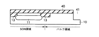
図示するように、本実施形態に係る半導体装置は、空洞11が形成されたSON領域と、空洞11の形成されないバルク領域とを備えている。SON領域の構造は、上記第1の実施形態と同様であるので説明は省略する。
【0042】
バルク領域においては、半導体基板10表面にウェル領域30が形成されている。このウェル領域30の表面に、ソース・ドレイン領域31、31が互いに離隔して形成されている。そして、ソース・ドレイン領域31、31間のウェル領域30上に、ゲート絶縁膜32を介在してゲート電極33が形成されている。また、ゲート電極33の側壁には、側壁絶縁膜34が形成されている。
【0043】
上記のようにして形成されたバルク領域内のMOSトランジスタは、素子分離領域13及び素子分離領域35によって周囲を取り囲まれている。ゲート電極33は、所定の方向に沿って延設され、その端部ではウェル領域30上から素子分離領域35上まで引き出されている。そして、素子分離領域35上に設けられたコンタクト領域36において、ゲート電極33に電位が与えられる。
【0044】
次に、上記半導体装置の製造方法について、図12乃至図16を用いて説明する。図12乃至図16は、半導体装置の製造工程を順次示す断面図である。
【0045】
まず、第1の実施形態で説明した工程に従って、半導体基板(例えばシリコン基板)10におけるSON領域に、空洞11及び素子分離領域13を形成する。すなわち図12に示すように、まず半導体基板10のSON領域に、トレンチ21を形成する。これらのトレンチ21は、空洞11の形成予定領域に形成される。
【0046】
次に、図13に示すように、マスク材20を除去し、非酸化性雰囲気中で高温アニールを行う。その結果、図示するような平板状の空洞11が、SON領域内に形成される。
【0047】
引き続き図14に示すように、SON領域にLOCOS法を用いて素子分離領域13を形成する。勿論、素子分離領域13は、空洞11の面内方向端部に接するようにして形成される。
【0048】
次に、半導体基板10のバルク領域内に、STI技術により素子分離領域35を形成する。すなわち、まず半導体基板10上に、マスク材40をCVD法等により形成する。マスク材40は、例えばシリコン酸化膜やシリコン窒化膜である。そして、リソグラフィ技術とRIEとによりマスク材40をパターニングして、素子分離領域35形成予定領域のマスク材40を除去する。更に、パターニングされたマスク材40をマスクに用いて半導体基板10をエッチングし、バルク領域の半導体基板10に図15に示すようなトレンチ41を形成する。
【0049】
次に、トレンチ41内をシリコン酸化膜等の絶縁膜で埋め込んだ後、マスク材40を除去し、素子分離領域35を形成する。その結果、図16に示すような、SON領域とバルク領域とが同一基板内に存在する構造が完成する。
【0050】
その後は、イオン注入法等によりバルク領域内にウェル領域30を形成する。更に、周知の方法により、SON領域及びバルク領域内に、それぞれMOSトランジスタを形成して、図11(a)、(b)に示す構造が完成する。
【0051】
上記のように、この発明の第2の実施形態に係る半導体装置及びその製造方法によれば、SON領域内の素子分離領域13をLOCOS法により形成しており、上記第1の実施形態と同様の効果が得られる。
【0052】
また、本実施形態に係る構造では、空洞11を設けたSON領域と、空洞11を設けないバルク領域とを、同一半導体基板内に形成している。この点に付き以下説明する。
【0053】
システムLSIにおいては、SONの使用の良否は回路毎に異なる。これはSONが本来的に有する基板浮遊効果の為である。すなわち、空洞11上の半導体層12は、半導体基板10と電気的に絶縁されているため、半導体層12の電位はフローティングである。すると、ディジタル動作を行う半導体素子は、空洞11上の半導体層12に形成されることが望ましい。他方、アナログ動作を行う半導体素子は、電位の安定しない半導体層12上に形成されることは望ましくない。
【0054】
本実施形態によれば、同一半導体基板上において、SON(半導体層12)上のMOSトランジスタと半導体基板10上のMOSトランジスタとを、半導体素子の特性によって使い分けることが出来る。従って、システムLSIの高速・高性能化が実現できる。
【0055】
なお、同一半導体基板10内にSON領域とバルク領域とを形成する方法は、上記図12乃至図16に示す方法に限られるものではない。図17乃至図19は、本実施形態の変形例に係る半導体装置の製造方法を順次示す断面図である。
【0056】
すなわち、図17に示すように、まずバルク領域内に素子分離領域35をSTI技術により形成する。次に図18に示すように、SON領域内に平板状の空洞11を形成する。その後図19に示すように、SON領域内に、空洞11に接する素子分離領域13を形成しても良い。
【0057】
次に、この発明の第3の実施形態に係る半導体装置について、図20を用いて説明する。本実施形態は、上記第2の実施形態を、DRAM混載型システムLSIに適用したものであり、図20は、DRAM混載型システムLSIの平面図である。
【0058】
図示するように、バルク領域にはDRAMセルアレイが設けられ、SON領域にはロジック回路が設けられている。そして、SON領域と接するバルク領域(以下境界領域と呼ぶ)に、DRAMセルのダミーパターンが設けられている。
【0059】
バルク領域中には複数の素子領域AA1が千鳥状に配置されている。図20において斜線の付された領域が素子領域AA1を示している。素子領域AA1以外の領域には素子分離領域が設けられている。素子領域は、長手方向が4F(F:最小加工寸法)、長手方向に直交する方向が2Fの幅で形成されている。DRAMセルアレイは、素子領域AA1内に設けられたセルトランジスタと、素子領域AA1の長手方向の両端部に接するようにして設けられたトレンチ型のセルキャパシタTCとを有するメモリセルを複数備えている。そして、同一列に位置するメモリセルにビット線コンタクトプラグBCを介して電気的に接続された複数のビット線BLが、素子領域AA1の長手方向に沿って設けられている。更に、同一行のセルトランジスタのゲート電極に電気的に接続された複数のワード線WLが、素子領域AA1の長手方向に直交する方向に沿って設けられている。
【0060】
境界領域には、DRAMセルと同様のパターンの素子領域AA1が形成されている。この素子領域はDRAMセルの形成には使用されないダミーパターンである。DRAM等では、膨大な数のメモリセルが規則性を持ってアレイ状に配置されている。しかし、DRAMセルアレイ端部ではその規則性が崩れる。すると、DRAMセルアレイ端部におけるリソグラフィ条件やエッチング条件に変動が起こり易くなり、メモリセルとしての信頼性の維持が困難となる。そのため、DRAMセルアレイの外部に、DRAMセルアレイと同一パターンのダミーパターンを形成することにより、DRAMセルアレイ内のメモリセルの信頼性を維持する手法が広く用いられている。本実施形態では、このダミーパターンを、バルク領域とSON領域との境界領域に設けている。
【0061】
SON領域中にはロジック回路が設けられる。ロジック回路の構成については省略する。
【0062】
次に図20に示すシステムLSIの断面構造について、図21を用いて説明する。図21は、図20におけるX3−X3’線方向に沿った断面図である。まずバルク領域内のDRAMセルアレイの構造について説明する。
【0063】
p型シリコン基板50中には、トレンチキャパシタTC形成用のトレンチ51が設けられている。このトレンチ51の上部を除いた内周面上にはキャパシタ絶縁膜52が設けられている。更にトレンチ51の上部を除いた内周面上で、且つキャパシタ絶縁膜52よりも上部には、キャパシタ絶縁膜52よりも膜厚の大きいカラー酸化膜53が設けられている。また、トレンチ51内にはストレージノード電極54がトレンチ51内部を途中まで埋め込むようにして設けられ、ストレージノード電極54上に更に導電体層55が設けられている。また、トレンチ51内の開口近傍に低抵抗の導電体層56が更に設けられている。そして、シリコン基板50中にキャパシタ絶縁膜52と接するようにしてn+型不純物拡散層57が設けられている。このn+型不純物拡散層57はプレート電極として機能する。更にシリコン基板50中には、複数のn+型不純物拡散層57と共通接続されたn型ウェル領域58が設けられている。以上のようにして、トレンチ型のセルキャパシタTCが形成されている。
【0064】
シリコン基板50上には、ゲート絶縁膜32を介在してゲート電極33が設けられており、絶縁膜34がゲート電極33を取り囲むようにして設けられている。また、シリコン基板50表面内にn+型ソース・ドレイン領域31、31が設けられることによりセルトランジスタが形成されている。そして、セルトランジスタのソース領域31とセルキャパシタTCの導電体層56とが電気的に接続されている。以上のようなセルトランジスタとセルキャパシタとを含むDRAMセルが、DRAMセルアレイ内に複数設けられている。またDRAMセルは、素子分離領域35によって電気的に互いに分離された素子領域AA1内に2個づつ配置され、ドレイン領域31を共有している。なお、上記第2の実施形態で説明したように、バルク領域中の素子分離領域35は、STI技術によって形成される。
【0065】
そして、上記DRAMセルを被覆するようにして、シリコン基板50上に層間絶縁膜60が設けられている。層間絶縁膜60内には、層間絶縁膜60表面からドレイン領域31に達するビット線コンタクトプラグBCが設けられている。そして層間絶縁膜60上に、ビット線コンタクトプラグBCと電気的に接続されたビット線BLが設けられている。
【0066】
境界領域、すなわちSON領域と接するバルク領域には、DRAMセルと同様のパターンの素子領域AA1が形成されているのみであり、半導体素子は形成されていない。但し、セルトランジスタのn+型不純物拡散層57と接続されるn型ウェル領域61が、シリコン基板50の表面に達するように形成されている。この領域において、n型ウェル領域61にプレート電位が与えられる。
【0067】
SON領域においては、上記第1、第2の実施形態で説明したように、半導体基板50の表面内に空洞11が形成されている。そして、空洞11上の半導体層12は、素子分離領域13によって取り囲まれている。勿論、素子分離領域13は、半導体基板50をLOCOS法によって酸化して形成したシリコン酸化膜であり、半導体層12は半導体基板50の一部である。半導体層12中には、ソース・ドレイン領域14、14が形成され、半導体層12上にはゲート絶縁膜15を介在してゲート電極16が形成されている。更に、ゲート電極の周囲を取り囲むようにして絶縁膜17が形成され、半導体基板50上には層間絶縁膜60が形成されている。
【0068】
そして上記DRAMセルアレイ、ダミーパターン、及びロジック回路を層間絶縁膜62が被覆している。
【0069】
上記のように、この発明の第3の実施形態に係る半導体装置によれば、リーク電流や閾値電圧に対して高度の制御性を求める回路、例えばDRAMセルアレイやセンスアンプ等をバルク領域内に形成し、ディジタル動作を行うロジック回路等をSON領域に形成している。従って、DRAMセルアレイやセンスアンプ、並びにロジック回路を、最適な条件下で動作させることが出来る。よって、システムLSIの高速化・高性能化が実現される。
【0070】
なお、本実施形態では境界領域には素子領域AA1を設けるのみであったが、更にトレンチキャパシタを形成しても良い。勿論、ダミーのメモリセルを形成しても良い。また、DRAM混載のシステムLSIに限らず、例えばSRAM(Static RAM)やフラッシュメモリ、Ferroelectric RAM、MRAM(Magnetoresistive RAM)等を有するシステムLSIであっても良い。また、本実施形態は半導体記憶装置を有するLSIに限られず、ロジック回路及びディジタル回路が混載された半導体装置であれば、広く一般に適用できる。
【0071】
上記のように、この発明の第1乃至第3の実施形態に係る半導体装置及びその製造方法によれば、SON構造における空洞間の素子分離領域を、LOCOS法によって形成している。また、素子分離領域は、空洞の面内方向端部に接するように形成される。従って、空洞と素子分離領域との間に無駄なスペースを必要とせず、またウェル分離等も必要としないので、半導体装置の微細化が可能となる。また、空洞のサイズはほぼ素子領域と同じで済むため、製造が容易となり、半導体装置の製造歩留まりが向上される。更に、ディジタル動作を行う回路に対してはSON構造を使用し、アナログ動作を行う回路に対してはバルクシリコンを使用することで、各回路が最適な条件下で動作出来る。その結果、システムLSIの高速化・高性能化が実現できる。
【0072】
なお、SON上のMOSトランジスタについて図22を用いて説明する。図22は、SON構造の断面図である。図示するように、最小加工寸法が0.1μmの世代のMOSトランジスタでは、半導体層12(素子領域AA)の幅W1は、約5000〜6000Å程度である。また、その厚さd2は、〜500Å程度である。なお、SON上のMOSトランジスタでは、半導体層12が薄いほどショートチャネル効果を防止できることが知られている。特に、ゲート長の1/4以下にすることが望ましい。
【0073】
半導体層12の膜厚は、図23に示すように、空洞11を形成するためのトレンチ22の開口幅によってほぼ決定される。すなわち、トレンチ22の開口幅をa1とすると、その後のアニールによって形成される半導体層12の膜厚もほぼa1となる。従って、半導体層12の膜厚d2を500Åにしたい場合には、トレンチ22の開口幅a1を500Åにすれば良い。
【0074】
このように、空洞11上の半導体層12の膜厚は非常に小さい。従って、素子分離領域13の深さも浅くて済む。すなわち、半導体層12とほぼ同程度の膜厚で済む。そのため、素子分離領域13をLOCOS法で形成したとしても、バーズビークは殆ど問題にならず、半導体装置の微細化が妨げられるものではない。
【0075】
なお、本願発明は上記実施形態に限定されるものではなく、実施段階ではその要旨を逸脱しない範囲で種々に変形することが可能である。更に、上記実施形態には種々の段階の発明が含まれており、開示される複数の構成要件における適宜な組み合わせにより種々の発明が抽出されうる。例えば、実施形態に示される全構成要件からいくつかの構成要件が削除されても、発明が解決しようとする課題の欄で述べた課題が解決でき、発明の効果の欄で述べられている効果が得られる場合には、この構成要件が削除された構成が発明として抽出されうる。
【0076】
【発明の効果】
以上説明したように、この発明によれば、微細化可能なSON構造を有する半導体装置及びその製造方法を提供出来る。
【図面の簡単な説明】
【図1】この発明の第1の実施形態に係る半導体装置を示しており、(a)図は平面図、(b)図は(a)図におけるX1−X1’線に沿った断面図。
【図2】この発明の第1の実施形態に係る半導体装置の第1の製造工程の断面図。
【図3】この発明の第1の実施形態に係る半導体装置の第2の製造工程の断面図。
【図4】この発明の第1の実施形態に係る半導体装置の第3の製造工程の断面図。
【図5】この発明の第1の実施形態に係る半導体装置の第4の製造工程の断面図。
【図6】この発明の第1の実施形態に係る半導体装置の第5の製造工程の断面図。
【図7】この発明の第1の実施形態に係る半導体装置の第6の製造工程の断面図。
【図8】この発明の第1の実施形態に係る半導体装置の第7の製造工程の断面図。
【図9】この発明の第1の実施形態に係る半導体装置の第8の製造工程の断面図。
【図10】この発明の第1の実施形態に係る半導体装置の第9の製造工程の断面図。
【図11】この発明の第2の実施形態に係る半導体装置を示しており、(a)図は平面図、(b)図は(a)図におけるX2−X2’線に沿った断面図。
【図12】この発明の第2の実施形態に係る半導体装置の第1の製造工程の断面図。
【図13】この発明の第2の実施形態に係る半導体装置の第2の製造工程の断面図。
【図14】この発明の第2の実施形態に係る半導体装置の第3の製造工程の断面図。
【図15】この発明の第2の実施形態に係る半導体装置の第4の製造工程の断面図。
【図16】この発明の第2の実施形態に係る半導体装置の第5の製造工程の断面図。
【図17】この発明の第2の実施形態の変形例に係る半導体装置の第1の製造工程の断面図。
【図18】この発明の第2の実施形態の変形例に係る半導体装置の第2の製造工程の断面図。
【図19】この発明の第2の実施形態の変形例に係る半導体装置の第3の製造工程の断面図。
【図20】この発明の第3の実施形態に係る半導体装置の平面図。
【図21】図20におけるX3−X3’線に沿った断面図。
【図22】この発明の第1乃至第3の実施形態に係る半導体装置の一部断面図。
【図23】この発明の第1乃至第3の実施形態に係る半導体装置の製造方法の一部工程の断面図。
【図24】従来の半導体装置の断面図。
【符号の説明】
10、50、100…半導体基板
11、23、110…空洞
12…半導体層
13、35、150…素子分離領域
14、31、120…ソース・ドレイン領域
15、32、130…ゲート絶縁膜
16、33、140…ゲート電極
17、34、170…側壁絶縁膜
18、36…コンタクト領域
20、24、25…マスク材
21、26…レジスト
22、51…トレンチ
30、160…ウェル領域
52…キャパシタ絶縁膜
53…絶縁膜
54…ストレージノード電極
55、56…導電膜
57…プレート電極
58、61…不純物拡散層
60、62…層間絶縁膜[0001]
BACKGROUND OF THE INVENTION
The present invention relates to a semiconductor device and a manufacturing method thereof. In particular, the present invention relates to a technique used for a system LSI using a SON (Silicon on Nothing) substrate.
[0002]
[Prior art]
SOI (Silicon on Insulator) has been widely known as a structure in which a silicon layer is formed on an insulating film. By forming a semiconductor element on such an SOI, it is possible to reduce the power consumption and the operation speed of the semiconductor integrated circuit. As a method for forming SOI, there are a method of bonding two substrates, a SIMOX (Separation by Implanted Oxygen) method, and the like. However, SOI has drawbacks such as high manufacturing cost and extremely difficult formation of a silicon layer with few defects.
[0003]
Therefore, in recent years, attention has been paid to a SON structure in which a silicon layer is formed on a cavity. SON can be said to be the ultimate SOI structure, and the same merit as SOI can be obtained. Currently, research on SON is actively conducted, and a method of insulating a semiconductor substrate and a silicon layer (see, for example, Patent Document 1), a method for manufacturing a miniaturized SON (see, for example, Patent Document 2), and SON Various researches have been made on a manufacturing method of a double gate MOS transistor (see, for example, Patent Document 3) and an infrared sensor using SON (see, for example, Patent Document 4).
[0004]
A structure of a conventional semiconductor device using the SON structure will be described with reference to FIG. 24 (for details, see, for example, Patent Document 5). FIG. 24 is a sectional view of a MOS transistor formed on the SON.
[0005]
As illustrated, a
[0006]
As described above, attempts to reduce the power consumption and the operating speed of the semiconductor integrated circuit by using the SON have been actively made. In the future, for example, SON is expected to be used in a system LSI or the like in which DRAM (Dynamic Random Access Memory) is embedded.
[0007]
[Patent Document 1]
JP-A-5-206257
[0008]
[Patent Document 2]
JP-A-8-288381
[0009]
[Patent Document 3]
JP 2001-257358 A
[0010]
[Patent Document 4]
JP 2001-281051 A
[0011]
[Patent Document 5]
Japanese Patent Laid-Open No. 2001-144276 (
[0012]
[Problems to be solved by the invention]
However, the conventional SON structure has a problem that it is difficult to miniaturize a semiconductor device.
[0013]
That is, as shown in FIG. 24, when the SON and STI techniques are used, the
[0014]
Further, in the conventional structure, the element region AA10 on the
[0015]
The present invention has been made in view of the above circumstances, and it is an object of the present invention to provide a semiconductor device having a SON structure that can be miniaturized and a method for manufacturing the same.
[0016]
[Means for Solving the Problems]
A semiconductor device according to a first aspect of the present invention is in contact with a semiconductor substrate, a flat cavity formed in the semiconductor substrate, and an end portion in the in-plane direction of the cavity in the surface of the semiconductor substrate. Formed as And partitioning the element region located on the cavity An element isolation region, and a bottom surface of the element isolation region is shallower than a bottom surface of the cavity and deeper than an upper surface of the cavity. The area of the upper surface of the cavity is larger than the area of the bottom surface of the element region. .
[0017]
According to a second aspect of the present invention, there is provided a semiconductor device including: a semiconductor substrate; a plurality of flat cavities formed in the semiconductor substrate; and the cavity in the surface of the semiconductor substrate between the adjacent cavities. End in the in-plane direction Formed in contact with And partitioning the element region located on the cavity An element isolation region, and a bottom surface of the element isolation region is shallower than a bottom surface of the cavity and deeper than an upper surface of the cavity. The area of the upper surface of the cavity is larger than the area of the bottom surface of the element region. .
[0018]
Furthermore, the method for manufacturing a semiconductor device according to one aspect of the present invention includes a step of partially forming a flat cavity in a semiconductor substrate, and a surface of the cavity on the surface of the semiconductor substrate between the adjacent cavities. Forming an insulating film so as to be in contact with an inward end, electrically separating element regions located on adjacent cavities, and forming a semiconductor element on the element region; The element region is partitioned by the separating step, The bottom surface of the insulating film is shallower than the bottom surface of the cavity and deeper than the top surface of the cavity. And the area of the upper surface of the cavity is larger than the area of the bottom surface of the element region. .
[0020]
Furthermore, a semiconductor device according to a third aspect of the present invention includes a first semiconductor layer formed on a first region of a semiconductor substrate and a second semiconductor layer formed on the second region of the semiconductor substrate with a cavity interposed therebetween. Two cavities on the semiconductor substrate between the two semiconductor layers and the first and second semiconductor layers End in the in-plane direction And an element isolation region that electrically isolates the first and second semiconductor layers, and the bottom surface of the element isolation region is shallower than the bottom surface of the cavity, and Deeper than the top surface The area of the upper surface of the cavity is larger than the area of the bottom surface of the second semiconductor layer. .
[0022]
DETAILED DESCRIPTION OF THE INVENTION
Embodiments of the present invention will be described below with reference to the drawings. In the description, common parts are denoted by common reference symbols throughout the drawings.
[0023]
A semiconductor device and a manufacturing method thereof according to a first embodiment of the present invention will be described with reference to FIGS. 1A is a plan view of a MOS transistor using SON, and FIG. 1B is a cross-sectional view taken along line X1-X1 ′ in FIG.
[0024]
As shown in the figure, a
[0025]
In the
[0026]
The
[0027]
As described above, the MOS transistor including the source /
[0028]
Next, a method for manufacturing the semiconductor device will be described with reference to FIGS. 2 to 10 are cross-sectional views sequentially showing manufacturing steps of the semiconductor device.
[0029]
First, as shown in FIG. 2, a
[0030]
Next, as shown in FIG. 3, the
[0031]
Next, the resist 21 is ashed and removed. Thereafter, as shown in FIG. 4, the
[0032]
Next, the
[0033]
Next, the
[0034]
Next, as shown in FIG. 8, the
[0035]
Next, as shown in FIG. 9, the surface of the
[0036]
Next, the
[0037]
Thereafter, the source /
[0038]
As described above, according to the semiconductor device and the manufacturing method thereof according to the first embodiment of the present invention, the
[0039]
If the
[0040]
A semiconductor device and a manufacturing method thereof according to the second embodiment of the present invention will be described with reference to FIGS. 11A is a plan view of a MOS transistor using SON, and FIG. 11B is a cross-sectional view taken along line X2-X2 ′ of FIG.
[0041]
As shown in the drawing, the semiconductor device according to the present embodiment includes an SON region in which the
[0042]
In the bulk region, a
[0043]
The MOS transistor in the bulk region formed as described above is surrounded by the
[0044]
Next, a method for manufacturing the semiconductor device will be described with reference to FIGS. 12 to 16 are cross-sectional views sequentially showing the manufacturing steps of the semiconductor device.
[0045]
First, according to the process described in the first embodiment, the
[0046]
Next, as shown in FIG. 13, the
[0047]
Subsequently, as shown in FIG. 14, the
[0048]
Next, an
[0049]
Next, after the
[0050]
Thereafter, the
[0051]
As described above, according to the semiconductor device and the manufacturing method thereof according to the second embodiment of the present invention, the
[0052]
In the structure according to this embodiment, the SON region provided with the
[0053]
In a system LSI, the quality of use of SON varies from circuit to circuit. This is because of the substrate floating effect inherent in SON. That is, since the
[0054]
According to this embodiment, on the same semiconductor substrate, the MOS transistor on the SON (semiconductor layer 12) and the MOS transistor on the
[0055]
The method for forming the SON region and the bulk region in the
[0056]
That is, as shown in FIG. 17, first, the
[0057]
Next, a semiconductor device according to a third embodiment of the present invention will be described with reference to FIG. In the present embodiment, the second embodiment is applied to a DRAM-embedded system LSI, and FIG. 20 is a plan view of the DRAM-embedded system LSI.
[0058]
As shown in the figure, a DRAM cell array is provided in the bulk region, and a logic circuit is provided in the SON region. A dummy pattern of a DRAM cell is provided in a bulk region (hereinafter referred to as a boundary region) in contact with the SON region.
[0059]
A plurality of element regions AA1 are arranged in a staggered pattern in the bulk region. In FIG. 20, the shaded area indicates the element area AA1. An element isolation region is provided in a region other than the element region AA1. The element region is formed with a width of 4F in the longitudinal direction (F: minimum processing dimension) and 2F in the direction orthogonal to the longitudinal direction. The DRAM cell array includes a plurality of memory cells each having a cell transistor provided in the element region AA1 and a trench type cell capacitor TC provided in contact with both ends in the longitudinal direction of the element region AA1. A plurality of bit lines BL electrically connected to the memory cells located in the same column via the bit line contact plug BC are provided along the longitudinal direction of the element region AA1. Further, a plurality of word lines WL electrically connected to the gate electrodes of the cell transistors in the same row are provided along a direction orthogonal to the longitudinal direction of the element region AA1.
[0060]
In the boundary region, an element region AA1 having the same pattern as that of the DRAM cell is formed. This element region is a dummy pattern that is not used for forming a DRAM cell. In a DRAM or the like, a huge number of memory cells are arranged in an array with regularity. However, the regularity is broken at the end of the DRAM cell array. As a result, the lithography conditions and the etching conditions at the edge of the DRAM cell array easily change, and it becomes difficult to maintain the reliability of the memory cell. Therefore, a technique for maintaining the reliability of the memory cells in the DRAM cell array by forming a dummy pattern having the same pattern as the DRAM cell array outside the DRAM cell array is widely used. In the present embodiment, this dummy pattern is provided in the boundary region between the bulk region and the SON region.
[0061]
A logic circuit is provided in the SON region. The configuration of the logic circuit is omitted.
[0062]
Next, a cross-sectional structure of the system LSI shown in FIG. 20 will be described with reference to FIG. 21 is a cross-sectional view taken along the line X3-X3 ′ in FIG. First, the structure of the DRAM cell array in the bulk region will be described.
[0063]
In the p-
[0064]
A
[0065]
An interlayer insulating
[0066]
In the boundary region, that is, the bulk region in contact with the SON region, only the element region AA1 having the same pattern as the DRAM cell is formed, and no semiconductor element is formed. However, n of the cell transistor + An n-
[0067]
In the SON region, as described in the first and second embodiments, the
[0068]
An interlayer insulating
[0069]
As described above, according to the semiconductor device of the third embodiment of the present invention, a circuit for obtaining a high degree of controllability with respect to leakage current and threshold voltage, for example, a DRAM cell array, a sense amplifier, etc. is formed in the bulk region. In addition, a logic circuit or the like that performs digital operation is formed in the SON region. Therefore, the DRAM cell array, sense amplifier, and logic circuit can be operated under optimum conditions. Therefore, high speed and high performance of the system LSI can be realized.
[0070]
In the present embodiment, only the element region AA1 is provided in the boundary region, but a trench capacitor may be further formed. Of course, a dummy memory cell may be formed. Further, the system LSI is not limited to a DRAM-embedded system LSI, and may be, for example, a system LSI having SRAM (Static RAM), flash memory, Ferroelectric RAM, MRAM (Magnetoresistive RAM), or the like. Further, the present embodiment is not limited to an LSI having a semiconductor memory device, and can be widely applied to any semiconductor device in which a logic circuit and a digital circuit are mixedly mounted.
[0071]
As described above, according to the semiconductor device and the manufacturing method thereof according to the first to third embodiments of the present invention, the element isolation region between the cavities in the SON structure is formed by the LOCOS method. The element isolation region is formed so as to be in contact with the in-plane direction end of the cavity. Therefore, no wasteful space is required between the cavity and the element isolation region, and well isolation is not required, so that the semiconductor device can be miniaturized. Further, since the size of the cavity can be almost the same as that of the element region, the manufacturing is facilitated, and the manufacturing yield of the semiconductor device is improved. Further, by using the SON structure for circuits that perform digital operations and using bulk silicon for circuits that perform analog operations, each circuit can operate under optimum conditions. As a result, the system LSI can be increased in speed and performance.
[0072]
The MOS transistor on the SON will be described with reference to FIG. FIG. 22 is a cross-sectional view of the SON structure. As shown in the figure, in a generation MOS transistor having a minimum processing dimension of 0.1 μm, the width W1 of the semiconductor layer 12 (element region AA) is about 5000 to 6000 mm. The thickness d2 is about ˜500 mm. It is known that the MOS transistor on the SON can prevent the short channel effect as the
[0073]
The film thickness of the
[0074]
Thus, the film thickness of the
[0075]
Note that the present invention is not limited to the above-described embodiment, and various modifications can be made without departing from the scope of the invention in the implementation stage. Furthermore, the above embodiments include inventions at various stages, and various inventions can be extracted by appropriately combining a plurality of disclosed constituent elements. For example, even if some constituent requirements are deleted from all the constituent requirements shown in the embodiment, the problem described in the column of the problem to be solved by the invention can be solved, and the effect described in the column of the effect of the invention Can be extracted as an invention.
[0076]
【The invention's effect】
As described above, according to the present invention, it is possible to provide a semiconductor device having a SON structure that can be miniaturized and a manufacturing method thereof.
[Brief description of the drawings]
1A and 1B show a semiconductor device according to a first embodiment of the present invention, in which FIG. 1A is a plan view, and FIG. 1B is a cross-sectional view taken along line X1-X1 ′ in FIG.
FIG. 2 is a cross-sectional view of a first manufacturing process of the semiconductor device according to the first embodiment of the invention.
FIG. 3 is a cross-sectional view of a second manufacturing step of the semiconductor device according to the first embodiment of the invention.
FIG. 4 is a cross-sectional view of a third manufacturing process of the semiconductor device according to the first embodiment of the invention.
FIG. 5 is a cross-sectional view of a fourth manufacturing process of the semiconductor device according to the first embodiment of the invention.
FIG. 6 is a cross-sectional view of a fifth manufacturing process of the semiconductor device according to the first embodiment of the invention.
FIG. 7 is a cross-sectional view of a sixth manufacturing process of the semiconductor device according to the first embodiment of the invention.
FIG. 8 is a cross-sectional view of a seventh manufacturing process of the semiconductor device according to the first embodiment of the invention.
FIG. 9 is a cross-sectional view of an eighth manufacturing process of the semiconductor device according to the first embodiment of the invention.
FIG. 10 is a cross-sectional view of a ninth manufacturing process of the semiconductor device according to the first embodiment of the invention.
11A and 11B show a semiconductor device according to a second embodiment of the present invention, in which FIG. 11A is a plan view, and FIG. 11B is a cross-sectional view taken along line X2-X2 ′ in FIG.
FIG. 12 is a cross-sectional view of the first manufacturing process of the semiconductor device according to the second embodiment of the invention.
FIG. 13 is a cross-sectional view of a second manufacturing process of the semiconductor device according to the second embodiment of the invention.
FIG. 14 is a cross-sectional view of a third manufacturing process of the semiconductor device according to the second embodiment of the invention.
FIG. 15 is a sectional view of a fourth manufacturing process of the semiconductor device according to the second embodiment of the invention.
FIG. 16 is a cross-sectional view of a fifth manufacturing process of the semiconductor device according to the second embodiment of the invention.
FIG. 17 is a cross-sectional view of a first manufacturing process of a semiconductor device according to a variation of the second embodiment of the present invention.
FIG. 18 is a cross-sectional view of a second manufacturing process of a semiconductor device according to a variation of the second embodiment of the present invention.
FIG. 19 is a cross-sectional view of a third manufacturing process of the semiconductor device according to the modification of the second embodiment of the present invention.
FIG. 20 is a plan view of a semiconductor device according to a third embodiment of the present invention.
21 is a cross-sectional view taken along line X3-X3 ′ in FIG.
FIG. 22 is a partial cross-sectional view of the semiconductor device according to the first to third embodiments of the present invention.
FIG. 23 is a cross-sectional view of a part of the manufacturing method of the semiconductor device according to the first to third embodiments of the present invention;
FIG. 24 is a cross-sectional view of a conventional semiconductor device.
[Explanation of symbols]
10, 50, 100 ... Semiconductor substrate
11, 23, 110 ... hollow
12 ... Semiconductor layer
13, 35, 150 ... element isolation region
14, 31, 120 ... source / drain regions
15, 32, 130 ... gate insulating film
16, 33, 140 ... gate electrode
17, 34, 170 ... sidewall insulating film
18, 36 ... contact area
20, 24, 25 ... mask material
21, 26 ... resist
22, 51 ... trench
30, 160 ... well region
52. Capacitor insulating film
53. Insulating film
54 ... Storage node electrode
55, 56 ... conductive film
57 ... Plate electrode
58, 61 ... Impurity diffusion layer
60, 62 ... interlayer insulation film
Claims (4)
前記半導体基板内に形成された平板状の空洞と、
前記半導体基板の表面内に、前記空洞の面内方向における端部に接するようにして形成され、前記空洞上に位置する素子領域を区画形成する素子分離領域と
を具備し、前記素子分離領域の底面は、前記空洞の底面よりも浅く、且つ前記空洞の上面よりも深い位置にあり、前記空洞上面の面積は、前記素子領域の底面の面積よりも大きいことを特徴とする半導体装置。A semiconductor substrate;
A flat cavity formed in the semiconductor substrate;
An element isolation region that is formed in the surface of the semiconductor substrate so as to be in contact with an end portion in the in-plane direction of the cavity, and that forms an element region located on the cavity; bottom, shallower than the bottom of the cavity, and Ri position near deeper than the upper surface of said cavity, the area of the cavity top surface, wherein a greater than the area of the bottom surface of the device region.
前記半導体基板内に複数形成された平板状の空洞と、
隣接する前記空洞間の前記半導体基板表面内に、前記空洞の面内方向における端部に接するようにして形成され、前記空洞上に位置する素子領域を区画形成する素子分離領域と
を具備し、前記素子分離領域の底面は、前記空洞の底面よりも浅く、且つ前記空洞の上面よりも深い位置にあり、前記空洞上面の面積は、前記素子領域の底面の面積よりも大きいことを特徴とする半導体装置。A semiconductor substrate;
A plurality of flat cavities formed in the semiconductor substrate;
An element isolation region that is formed in the surface of the semiconductor substrate between the adjacent cavities so as to be in contact with an end portion in the in-plane direction of the cavity, and that defines an element region located on the cavity; bottom of the device isolation region is shallower than a bottom surface of the cavity, and the area of the deep position near is, the cavity top surface than the top surface of the cavity, and being greater than the area of the bottom surface of the device region Semiconductor device.
前記半導体基板の第2領域上に、空洞を介在して形成された第2半導体層と、
前記第1、第2半導体層間の前記半導体基板上に、前記空洞の面内方向における端部に接するようにして形成され、前記第1、第2半導体層を電気的に分離する素子分離領域と
を具備し、前記素子分離領域の底面は、前記空洞の底面よりも浅く、且つ前記空洞の上面よりも深い位置にあり、前記空洞上面の面積は、前記第2半導体層の底面の面積よりも大きいことを特徴とする半導体装置。A first semiconductor layer formed on the first region of the semiconductor substrate;
A second semiconductor layer formed on the second region of the semiconductor substrate with a cavity interposed therebetween;
An element isolation region formed on the semiconductor substrate between the first and second semiconductor layers so as to be in contact with an end portion in the in-plane direction of the cavity and electrically separating the first and second semiconductor layers; comprising a bottom surface of the isolation region is shallower than a bottom surface of the cavity, and Ri position near deeper than the upper surface of said cavity, the area of the cavity top surface, from the area of the bottom surface of the second semiconductor layer A large semiconductor device.
隣接する前記空洞間の前記半導体基板表面に、該空洞の面内方向端部に接するように絶縁膜を形成して、隣接する空洞上に位置する素子領域間を電気的に分離する工程と、
前記素子領域上に半導体素子を形成する工程と
を具備し、前記分離する工程により前記素子領域は区画形成され、前記絶縁膜の底面は、前記空洞の底面よりも浅く、且つ前記空洞の上面よりも深い位置に形成され、前記空洞上面の面積は前記素子領域の底面の面積よりも大きく形成されることを特徴とする半導体装置の製造方法。A step of partially forming a flat cavity in a semiconductor substrate;
Forming an insulating film on the surface of the semiconductor substrate between the adjacent cavities so as to be in contact with the in-plane direction end of the cavities, and electrically separating element regions located on the adjacent cavities;
Forming a semiconductor element on the element region, wherein the element region is defined by the separating step , and the bottom surface of the insulating film is shallower than the bottom surface of the cavity and from the top surface of the cavity. The method for manufacturing a semiconductor device is characterized in that the upper surface area of the cavity is formed larger than the area of the bottom surface of the element region .
Priority Applications (3)
| Application Number | Priority Date | Filing Date | Title |
|---|---|---|---|
| JP2002273409A JP4031329B2 (en) | 2002-09-19 | 2002-09-19 | Semiconductor device and manufacturing method thereof |
| US10/665,614 US7009273B2 (en) | 2002-09-19 | 2003-09-19 | Semiconductor device with a cavity therein and a method of manufacturing the same |
| US11/315,796 US7145215B2 (en) | 2002-09-19 | 2005-12-22 | Semiconductor device with a cavity therein and a method of manufacturing the same |
Applications Claiming Priority (1)
| Application Number | Priority Date | Filing Date | Title |
|---|---|---|---|
| JP2002273409A JP4031329B2 (en) | 2002-09-19 | 2002-09-19 | Semiconductor device and manufacturing method thereof |
Publications (3)
| Publication Number | Publication Date |
|---|---|
| JP2004111721A JP2004111721A (en) | 2004-04-08 |
| JP2004111721A5 JP2004111721A5 (en) | 2005-08-25 |
| JP4031329B2 true JP4031329B2 (en) | 2008-01-09 |
Family
ID=32270175
Family Applications (1)
| Application Number | Title | Priority Date | Filing Date |
|---|---|---|---|
| JP2002273409A Expired - Fee Related JP4031329B2 (en) | 2002-09-19 | 2002-09-19 | Semiconductor device and manufacturing method thereof |
Country Status (2)
| Country | Link |
|---|---|
| US (2) | US7009273B2 (en) |
| JP (1) | JP4031329B2 (en) |
Families Citing this family (60)
| Publication number | Priority date | Publication date | Assignee | Title |
|---|---|---|---|---|
| JP4074051B2 (en) * | 1999-08-31 | 2008-04-09 | 株式会社東芝 | Semiconductor substrate and manufacturing method thereof |
| US7173841B2 (en) * | 2004-12-03 | 2007-02-06 | Taiwan Semiconductor Manufacturing Company, Ltd. | Magnetic memory array |
| US7071047B1 (en) * | 2005-01-28 | 2006-07-04 | International Business Machines Corporation | Method of forming buried isolation regions in semiconductor substrates and semiconductor devices with buried isolation regions |
| EP1770055B1 (en) * | 2005-09-28 | 2008-05-28 | STMicroelectronics S.r.l. | Process for manufacturing thick suspended structures of semiconductor material |
| US8395199B2 (en) * | 2006-03-25 | 2013-03-12 | 4D-S Pty Ltd. | Systems and methods for fabricating self-aligned memory cell |
| US7285480B1 (en) * | 2006-04-07 | 2007-10-23 | International Business Machines Corporation | Integrated circuit chip with FETs having mixed body thicknesses and method of manufacture thereof |
| US7932548B2 (en) * | 2006-07-14 | 2011-04-26 | 4D-S Pty Ltd. | Systems and methods for fabricating self-aligned memory cell |
| US8305829B2 (en) * | 2009-02-23 | 2012-11-06 | Taiwan Semiconductor Manufacturing Company, Ltd. | Memory power gating circuit for controlling internal voltage of a memory array, system and method for controlling the same |
| US8305790B2 (en) * | 2009-03-16 | 2012-11-06 | Taiwan Semiconductor Manufacturing Company, Ltd. | Electrical anti-fuse and related applications |
| US8957482B2 (en) * | 2009-03-31 | 2015-02-17 | Taiwan Semiconductor Manufacturing Company, Ltd. | Electrical fuse and related applications |
| US8912602B2 (en) * | 2009-04-14 | 2014-12-16 | Taiwan Semiconductor Manufacturing Company, Ltd. | FinFETs and methods for forming the same |
| US8461015B2 (en) * | 2009-07-08 | 2013-06-11 | Taiwan Semiconductor Manufacturing Company, Ltd. | STI structure and method of forming bottom void in same |
| US8759943B2 (en) | 2010-10-08 | 2014-06-24 | Taiwan Semiconductor Manufacturing Company, Ltd. | Transistor having notched fin structure and method of making the same |
| US8629478B2 (en) * | 2009-07-31 | 2014-01-14 | Taiwan Semiconductor Manufacturing Company, Ltd. | Fin structure for high mobility multiple-gate transistor |
| US8187928B2 (en) | 2010-09-21 | 2012-05-29 | Taiwan Semiconductor Manufacturing Company, Ltd. | Methods of forming integrated circuits |
| US8264032B2 (en) | 2009-09-01 | 2012-09-11 | Taiwan Semiconductor Manufacturing Company, Ltd. | Accumulation type FinFET, circuits and fabrication method thereof |
| US8482073B2 (en) * | 2010-03-25 | 2013-07-09 | Taiwan Semiconductor Manufacturing Company, Ltd. | Integrated circuit including FINFETs and methods for forming the same |
| US8264021B2 (en) * | 2009-10-01 | 2012-09-11 | Taiwan Semiconductor Manufacturing Company, Ltd. | Finfets and methods for forming the same |
| US8497528B2 (en) | 2010-05-06 | 2013-07-30 | Taiwan Semiconductor Manufacturing Company, Ltd. | Method for fabricating a strained structure |
| US8623728B2 (en) * | 2009-07-28 | 2014-01-07 | Taiwan Semiconductor Manufacturing Company, Ltd. | Method for forming high germanium concentration SiGe stressor |
| US8298925B2 (en) | 2010-11-08 | 2012-10-30 | Taiwan Semiconductor Manufacturing Company, Ltd. | Mechanisms for forming ultra shallow junction |
| US8472227B2 (en) * | 2010-01-27 | 2013-06-25 | Taiwan Semiconductor Manufacturing Company, Ltd. | Integrated circuits and methods for forming the same |
| US9484462B2 (en) * | 2009-09-24 | 2016-11-01 | Taiwan Semiconductor Manufacturing Company, Ltd. | Fin structure of fin field effect transistor |
| US8440517B2 (en) | 2010-10-13 | 2013-05-14 | Taiwan Semiconductor Manufacturing Company, Ltd. | FinFET and method of fabricating the same |
| US8980719B2 (en) | 2010-04-28 | 2015-03-17 | Taiwan Semiconductor Manufacturing Company, Ltd. | Methods for doping fin field-effect transistors |
| US9343463B2 (en) * | 2009-09-29 | 2016-05-17 | Headway Technologies, Inc. | Method of high density memory fabrication |
| US20110097867A1 (en) * | 2009-10-22 | 2011-04-28 | Taiwan Semiconductor Manufacturing Company, Ltd. | Method of controlling gate thicknesses in forming fusi gates |
| US9040393B2 (en) | 2010-01-14 | 2015-05-26 | Taiwan Semiconductor Manufacturing Company, Ltd. | Method of forming semiconductor structure |
| US8674472B2 (en) * | 2010-08-10 | 2014-03-18 | International Business Machines Corporation | Low harmonic RF switch in SOI |
| US8603924B2 (en) | 2010-10-19 | 2013-12-10 | Taiwan Semiconductor Manufacturing Company, Ltd. | Methods of forming gate dielectric material |
| US9048181B2 (en) | 2010-11-08 | 2015-06-02 | Taiwan Semiconductor Manufacturing Company, Ltd. | Mechanisms for forming ultra shallow junction |
| US8769446B2 (en) | 2010-11-12 | 2014-07-01 | Taiwan Semiconductor Manufacturing Company, Ltd. | Method and device for increasing fin device density for unaligned fins |
| US8592915B2 (en) | 2011-01-25 | 2013-11-26 | Taiwan Semiconductor Manufacturing Company, Ltd. | Doped oxide for shallow trench isolation (STI) |
| US8877602B2 (en) | 2011-01-25 | 2014-11-04 | Taiwan Semiconductor Manufacturing Company, Ltd. | Mechanisms of doping oxide for forming shallow trench isolation |
| US8431453B2 (en) | 2011-03-31 | 2013-04-30 | Taiwan Semiconductor Manufacturing Company, Ltd. | Plasma doping to reduce dielectric loss during removal of dummy layers in a gate structure |
| JP5891597B2 (en) * | 2011-04-07 | 2016-03-23 | 富士電機株式会社 | Manufacturing method of semiconductor substrate or semiconductor device |
| CN102842615B (en) * | 2011-06-20 | 2016-02-17 | 中国科学院微电子研究所 | A kind of semiconductor structure and manufacture method thereof |
| CN102856360B (en) * | 2011-06-27 | 2015-09-16 | 中国科学院微电子研究所 | A kind of semiconductor structure and manufacture method thereof |
| CN102856375B (en) * | 2011-06-27 | 2015-05-20 | 中国科学院微电子研究所 | Semiconductor structure and manufacturing method thereof |
| US8994127B2 (en) | 2011-11-24 | 2015-03-31 | Infineon Technologies Ag | Method of fabricating isolating semiconductor structures using a layout of trenches and openings |
| CN103377925A (en) * | 2012-04-13 | 2013-10-30 | 中国科学院微电子研究所 | Semiconductor structure and manufacture method thereof |
| CN103730361B (en) * | 2012-10-10 | 2018-02-13 | 中国科学院微电子研究所 | Method, semi-conductor device manufacturing method |
| US9437470B2 (en) | 2013-10-08 | 2016-09-06 | Cypress Semiconductor Corporation | Self-aligned trench isolation in integrated circuits |
| CN104681556B (en) * | 2013-11-28 | 2017-12-05 | 中芯国际集成电路制造(上海)有限公司 | A kind of integrated circuit and its manufacture method and electronic installation |
| US9252026B2 (en) | 2014-03-12 | 2016-02-02 | Cypress Semiconductor Corporation | Buried trench isolation in integrated circuits |
| DE102016119799B4 (en) * | 2016-10-18 | 2020-08-06 | Infineon Technologies Ag | INTEGRATED CIRCUIT CONTAINING A CURVED CAVE AND PRODUCTION METHOD |
| US10461152B2 (en) | 2017-07-10 | 2019-10-29 | Globalfoundries Inc. | Radio frequency switches with air gap structures |
| US10833153B2 (en) | 2017-09-13 | 2020-11-10 | Globalfoundries Inc. | Switch with local silicon on insulator (SOI) and deep trench isolation |
| US10109638B1 (en) * | 2017-10-23 | 2018-10-23 | Globalfoundries Singapore Pte. Ltd. | Embedded non-volatile memory (NVM) on fully depleted silicon-on-insulator (FD-SOI) substrate |
| US10446643B2 (en) | 2018-01-22 | 2019-10-15 | Globalfoundries Inc. | Sealed cavity structures with a planar surface |
| US10156676B1 (en) | 2018-02-26 | 2018-12-18 | Globalfoundries Inc. | Waveguides with multiple airgaps arranged in and over a silicon-on-insulator substrate |
| US10393960B1 (en) | 2018-02-26 | 2019-08-27 | Globalfoundries Inc. | Waveguides with multiple-level airgaps |
| US11056382B2 (en) * | 2018-03-19 | 2021-07-06 | Globalfoundries U.S. Inc. | Cavity formation within and under semiconductor devices |
| CN108682649B (en) * | 2018-04-17 | 2021-02-05 | 中芯集成电路(宁波)有限公司 | SOI substrate, semiconductor device and forming method thereof |
| US11410872B2 (en) | 2018-11-30 | 2022-08-09 | Globalfoundries U.S. Inc. | Oxidized cavity structures within and under semiconductor devices |
| US10923577B2 (en) | 2019-01-07 | 2021-02-16 | Globalfoundries U.S. Inc. | Cavity structures under shallow trench isolation regions |
| CN109935628B (en) * | 2019-03-27 | 2021-01-19 | 中国科学院上海微系统与信息技术研究所 | Anti-radiation transistor based on graphical SOI substrate and manufacturing method thereof |
| US11127816B2 (en) | 2020-02-14 | 2021-09-21 | Globalfoundries U.S. Inc. | Heterojunction bipolar transistors with one or more sealed airgap |
| KR20230013753A (en) * | 2021-07-20 | 2023-01-27 | 삼성전자주식회사 | Semiconductor device |
| US11650382B1 (en) * | 2021-10-26 | 2023-05-16 | Globalfoundries U.S. Inc. | Optical components undercut by a sealed cavity |
Family Cites Families (12)
| Publication number | Priority date | Publication date | Assignee | Title |
|---|---|---|---|---|
| US5227658A (en) | 1991-10-23 | 1993-07-13 | International Business Machines Corporation | Buried air dielectric isolation of silicon islands |
| US5567982A (en) * | 1994-09-30 | 1996-10-22 | Bartelink; Dirk J. | Air-dielectric transmission lines for integrated circuits |
| JPH08288381A (en) | 1995-04-19 | 1996-11-01 | Nissan Motor Co Ltd | Manufacture of semiconductor device |
| JP3762136B2 (en) * | 1998-04-24 | 2006-04-05 | 株式会社東芝 | Semiconductor device |
| JP4074051B2 (en) | 1999-08-31 | 2008-04-09 | 株式会社東芝 | Semiconductor substrate and manufacturing method thereof |
| JP3571989B2 (en) | 2000-03-13 | 2004-09-29 | 株式会社東芝 | Semiconductor device and manufacturing method thereof |
| JP3946406B2 (en) | 2000-03-30 | 2007-07-18 | 株式会社東芝 | Manufacturing method of thermal infrared sensor |
| US6670234B2 (en) * | 2001-06-22 | 2003-12-30 | International Business Machines Corporation | Method of integrating volatile and non-volatile memory cells on the same substrate and a semiconductor memory device thereof |
| US6630714B2 (en) * | 2001-12-27 | 2003-10-07 | Kabushiki Kaisha Toshiba | Semiconductor device formed in semiconductor layer arranged on substrate with one of insulating film and cavity interposed between the substrate and the semiconductor layer |
| JP2003243528A (en) * | 2002-02-13 | 2003-08-29 | Toshiba Corp | Semiconductor device |
| JP4277481B2 (en) | 2002-05-08 | 2009-06-10 | 日本電気株式会社 | Semiconductor substrate manufacturing method and semiconductor device manufacturing method |
| US6830987B1 (en) * | 2003-06-13 | 2004-12-14 | Advanced Micro Devices, Inc. | Semiconductor device with a silicon-on-void structure and method of making the same |
-
2002
- 2002-09-19 JP JP2002273409A patent/JP4031329B2/en not_active Expired - Fee Related
-
2003
- 2003-09-19 US US10/665,614 patent/US7009273B2/en not_active Expired - Fee Related
-
2005
- 2005-12-22 US US11/315,796 patent/US7145215B2/en not_active Expired - Fee Related
Also Published As
| Publication number | Publication date |
|---|---|
| US20040129998A1 (en) | 2004-07-08 |
| US7009273B2 (en) | 2006-03-07 |
| US7145215B2 (en) | 2006-12-05 |
| US20060157789A1 (en) | 2006-07-20 |
| JP2004111721A (en) | 2004-04-08 |
Similar Documents
| Publication | Publication Date | Title |
|---|---|---|
| JP4031329B2 (en) | Semiconductor device and manufacturing method thereof | |
| KR100671876B1 (en) | Semiconductor device and method of producing the same | |
| JP3825688B2 (en) | Manufacturing method of semiconductor device | |
| US6376316B2 (en) | Method for manufacturing semiconductor integrated circuit device having deposited layer for gate insulation | |
| JP3963970B2 (en) | DRAM cell and method of forming the same | |
| KR100525331B1 (en) | Semiconductor device | |
| JP3934507B2 (en) | Semiconductor memory device and manufacturing method of semiconductor memory device | |
| KR0163759B1 (en) | Semiconductor device and semiconductor memory device | |
| US10062581B2 (en) | Methods of forming an isolation structure and methods of manufacturing a semiconductor device including the same | |
| US9202921B2 (en) | Semiconductor device and method of making the same | |
| JP2008010503A (en) | Semiconductor memory device and its manufacturing method | |
| JP2004214379A (en) | Semiconductor device, method for manufacturing the same dynamic type semiconductor storage device, | |
| JPH10321813A (en) | Semiconductor memory device and its manufacture | |
| JP2004281782A (en) | Semiconductor device and its manufacturing method | |
| KR20090107822A (en) | Semiconductor device and method for manufacturing the same | |
| JP5583315B2 (en) | Semiconductor device and manufacturing method thereof | |
| JP2006049413A (en) | Semiconductor device and its manufacturing method | |
| KR101287733B1 (en) | Semiconductor device, method for manufacturing same, and semiconductor storage device | |
| US20080157162A1 (en) | Method of combining floating body cell and logic transistors | |
| US20040248364A1 (en) | Method of forming a memory cell with a single sided buried strap | |
| JP2006073813A (en) | Direct tunneling semiconductor memory and manufacturing method thereof | |
| JPH05190795A (en) | Memory cell array | |
| JP2013069770A (en) | Semiconductor device and manufacturing method of the same | |
| US20050184326A1 (en) | Deep-trench 1t-sram with buried out diffusion well merged with an ion implantation well | |
| JP5132120B2 (en) | GAIN CELL AND METHOD FOR MANUFACTURING AND USING THE SAME |
Legal Events
| Date | Code | Title | Description |
|---|---|---|---|
| A521 | Request for written amendment filed |
Free format text: JAPANESE INTERMEDIATE CODE: A523 Effective date: 20050208 |
|
| A621 | Written request for application examination |
Free format text: JAPANESE INTERMEDIATE CODE: A621 Effective date: 20050208 |
|
| A977 | Report on retrieval |
Free format text: JAPANESE INTERMEDIATE CODE: A971007 Effective date: 20060814 |
|
| A131 | Notification of reasons for refusal |
Free format text: JAPANESE INTERMEDIATE CODE: A131 Effective date: 20060829 |
|
| A521 | Request for written amendment filed |
Free format text: JAPANESE INTERMEDIATE CODE: A523 Effective date: 20061030 |
|
| A131 | Notification of reasons for refusal |
Free format text: JAPANESE INTERMEDIATE CODE: A131 Effective date: 20070710 |
|
| A521 | Request for written amendment filed |
Free format text: JAPANESE INTERMEDIATE CODE: A523 Effective date: 20070906 |
|
| TRDD | Decision of grant or rejection written | ||
| A01 | Written decision to grant a patent or to grant a registration (utility model) |
Free format text: JAPANESE INTERMEDIATE CODE: A01 Effective date: 20071016 |
|
| A61 | First payment of annual fees (during grant procedure) |
Free format text: JAPANESE INTERMEDIATE CODE: A61 Effective date: 20071018 |
|
| FPAY | Renewal fee payment (event date is renewal date of database) |
Free format text: PAYMENT UNTIL: 20101026 Year of fee payment: 3 |
|
| FPAY | Renewal fee payment (event date is renewal date of database) |
Free format text: PAYMENT UNTIL: 20111026 Year of fee payment: 4 |
|
| FPAY | Renewal fee payment (event date is renewal date of database) |
Free format text: PAYMENT UNTIL: 20111026 Year of fee payment: 4 |
|
| FPAY | Renewal fee payment (event date is renewal date of database) |
Free format text: PAYMENT UNTIL: 20121026 Year of fee payment: 5 |
|
| FPAY | Renewal fee payment (event date is renewal date of database) |
Free format text: PAYMENT UNTIL: 20131026 Year of fee payment: 6 |
|
| LAPS | Cancellation because of no payment of annual fees |