JP4025366B2 - Optical device for laser diode systems - Google Patents
Optical device for laser diode systems Download PDFInfo
- Publication number
- JP4025366B2 JP4025366B2 JP52135996A JP52135996A JP4025366B2 JP 4025366 B2 JP4025366 B2 JP 4025366B2 JP 52135996 A JP52135996 A JP 52135996A JP 52135996 A JP52135996 A JP 52135996A JP 4025366 B2 JP4025366 B2 JP 4025366B2
- Authority
- JP
- Japan
- Prior art keywords
- optical device
- axis
- emitter
- collimating
- emitters
- Prior art date
- Legal status (The legal status is an assumption and is not a legal conclusion. Google has not performed a legal analysis and makes no representation as to the accuracy of the status listed.)
- Expired - Fee Related
Links
Images


Classifications
-
- G—PHYSICS
- G02—OPTICS
- G02B—OPTICAL ELEMENTS, SYSTEMS OR APPARATUS
- G02B19/00—Condensers, e.g. light collectors or similar non-imaging optics
- G02B19/0033—Condensers, e.g. light collectors or similar non-imaging optics characterised by the use
- G02B19/0047—Condensers, e.g. light collectors or similar non-imaging optics characterised by the use for use with a light source
- G02B19/0052—Condensers, e.g. light collectors or similar non-imaging optics characterised by the use for use with a light source the light source comprising a laser diode
- G02B19/0057—Condensers, e.g. light collectors or similar non-imaging optics characterised by the use for use with a light source the light source comprising a laser diode in the form of a laser diode array, e.g. laser diode bar
-
- G—PHYSICS
- G02—OPTICS
- G02B—OPTICAL ELEMENTS, SYSTEMS OR APPARATUS
- G02B19/00—Condensers, e.g. light collectors or similar non-imaging optics
- G02B19/0004—Condensers, e.g. light collectors or similar non-imaging optics characterised by the optical means employed
- G02B19/0009—Condensers, e.g. light collectors or similar non-imaging optics characterised by the optical means employed having refractive surfaces only
- G02B19/0014—Condensers, e.g. light collectors or similar non-imaging optics characterised by the optical means employed having refractive surfaces only at least one surface having optical power
-
- G—PHYSICS
- G02—OPTICS
- G02B—OPTICAL ELEMENTS, SYSTEMS OR APPARATUS
- G02B27/00—Optical systems or apparatus not provided for by any of the groups G02B1/00 - G02B26/00, G02B30/00
- G02B27/09—Beam shaping, e.g. changing the cross-sectional area, not otherwise provided for
-
- G—PHYSICS
- G02—OPTICS
- G02B—OPTICAL ELEMENTS, SYSTEMS OR APPARATUS
- G02B27/00—Optical systems or apparatus not provided for by any of the groups G02B1/00 - G02B26/00, G02B30/00
- G02B27/09—Beam shaping, e.g. changing the cross-sectional area, not otherwise provided for
- G02B27/0938—Using specific optical elements
- G02B27/095—Refractive optical elements
- G02B27/0955—Lenses
- G02B27/0966—Cylindrical lenses
-
- G—PHYSICS
- G02—OPTICS
- G02B—OPTICAL ELEMENTS, SYSTEMS OR APPARATUS
- G02B6/00—Light guides; Structural details of arrangements comprising light guides and other optical elements, e.g. couplings
- G02B6/24—Coupling light guides
- G02B6/42—Coupling light guides with opto-electronic elements
- G02B6/4201—Packages, e.g. shape, construction, internal or external details
- G02B6/4249—Packages, e.g. shape, construction, internal or external details comprising arrays of active devices and fibres
-
- H—ELECTRICITY
- H01—ELECTRIC ELEMENTS
- H01S—DEVICES USING THE PROCESS OF LIGHT AMPLIFICATION BY STIMULATED EMISSION OF RADIATION [LASER] TO AMPLIFY OR GENERATE LIGHT; DEVICES USING STIMULATED EMISSION OF ELECTROMAGNETIC RADIATION IN WAVE RANGES OTHER THAN OPTICAL
- H01S5/00—Semiconductor lasers
- H01S5/40—Arrangement of two or more semiconductor lasers, not provided for in groups H01S5/02 - H01S5/30
- H01S5/4025—Array arrangements, e.g. constituted by discrete laser diodes or laser bar
-
- G—PHYSICS
- G02—OPTICS
- G02B—OPTICAL ELEMENTS, SYSTEMS OR APPARATUS
- G02B6/00—Light guides; Structural details of arrangements comprising light guides and other optical elements, e.g. couplings
- G02B6/24—Coupling light guides
- G02B6/42—Coupling light guides with opto-electronic elements
- G02B6/4201—Packages, e.g. shape, construction, internal or external details
- G02B6/4249—Packages, e.g. shape, construction, internal or external details comprising arrays of active devices and fibres
- G02B6/425—Optical features
-
- H—ELECTRICITY
- H01—ELECTRIC ELEMENTS
- H01S—DEVICES USING THE PROCESS OF LIGHT AMPLIFICATION BY STIMULATED EMISSION OF RADIATION [LASER] TO AMPLIFY OR GENERATE LIGHT; DEVICES USING STIMULATED EMISSION OF ELECTROMAGNETIC RADIATION IN WAVE RANGES OTHER THAN OPTICAL
- H01S3/00—Lasers, i.e. devices using stimulated emission of electromagnetic radiation in the infrared, visible or ultraviolet wave range
- H01S3/005—Optical devices external to the laser cavity, specially adapted for lasers, e.g. for homogenisation of the beam or for manipulating laser pulses, e.g. pulse shaping
-
- H—ELECTRICITY
- H01—ELECTRIC ELEMENTS
- H01S—DEVICES USING THE PROCESS OF LIGHT AMPLIFICATION BY STIMULATED EMISSION OF RADIATION [LASER] TO AMPLIFY OR GENERATE LIGHT; DEVICES USING STIMULATED EMISSION OF ELECTROMAGNETIC RADIATION IN WAVE RANGES OTHER THAN OPTICAL
- H01S5/00—Semiconductor lasers
- H01S5/005—Optical components external to the laser cavity, specially adapted therefor, e.g. for homogenisation or merging of the beams or for manipulating laser pulses, e.g. pulse shaping
-
- H—ELECTRICITY
- H01—ELECTRIC ELEMENTS
- H01S—DEVICES USING THE PROCESS OF LIGHT AMPLIFICATION BY STIMULATED EMISSION OF RADIATION [LASER] TO AMPLIFY OR GENERATE LIGHT; DEVICES USING STIMULATED EMISSION OF ELECTROMAGNETIC RADIATION IN WAVE RANGES OTHER THAN OPTICAL
- H01S5/00—Semiconductor lasers
- H01S5/40—Arrangement of two or more semiconductor lasers, not provided for in groups H01S5/02 - H01S5/30
- H01S5/4012—Beam combining, e.g. by the use of fibres, gratings, polarisers, prisms
Landscapes
- Physics & Mathematics (AREA)
- General Physics & Mathematics (AREA)
- Optics & Photonics (AREA)
- Condensed Matter Physics & Semiconductors (AREA)
- Electromagnetism (AREA)
- Semiconductor Lasers (AREA)
- Optical Couplings Of Light Guides (AREA)
Description
【技術分野】
【0001】
本発明は、光電要素からの光線を互いに垂直で且つ光学軸に垂直な2つの座標方向に視準し及び次いで高い光線密度で焦点に集光する装置に関し、特に特許請求の範囲第1項の前提部分による装置に関する。
【背景技術】
【0002】
半導体ダイオードレーザの光線は大きく分散されることを特徴とし、しかもレーザ光線は数mradの範囲内で僅かな光線の分散を伴って数ミリの直径を有する他の従来のレーザ光線源とは異なり、半導体ダイオードレーザの分散は1000mrad以上であることは既に知られている。
【0003】
半導体ダイオードレーザ光線を利用できるようにするため視準及び焦点合わせを行なうマイクロ光学又は光学装置が必要である。この場合、半導体レーザダイオードは通常、複数のエミッタ又はエミッタ群を一列に、しかも数100ミクロンの間隔で備えていることを考慮すべきである。光学装置又はマイクロ光学器械を設計する場合、使用されるレンズはその時の半導体ダイオードレーザもしくは相応のレーザ装置に又はチップに密集して設置されねばならないので、個々のエミッタ又はエミッタ群のレーザ光線は光学装置に入る前に殆ど重ならず、他の場合には許容し得ない又は適切でない投射角に基づき光の散乱により相当なビーム損失が生じることを考慮しなければならない。さらに、半導体レーザダイオードでは活性層に垂直な面(Fast-Axis)における分散角は活性層の面(Slow-Axis)における分散角より大きいことも光学装置を設計する際に考慮すべきである。
【0004】
エミッタ又はエミッタ群の分散するレーザ光線を光学軸に相前後して配置された2つの円筒レンズによって視準することは既に知られており、その場合第1の円筒レンズによって速動軸(Fast-Axis)、即ち活性層の面に垂直な軸線方向の視準を行い及びレーザダイオード装置から一層離れた第2の円筒レンズによって緩動軸(Slow-Axis)の方向の視準を行なう。
【0005】
この場合、特にまた光学装置(US 3396344)が知られており、該装置では複数のレーザダイオード又はエミッタもしくはエミッタ群が少なくとも2列に重ねられて設置され、その各列は第1の座標方向において活性層の面に複数のエミッタ又はエミッタ群を備え及び2つの列は活性層に垂直な第2の座標方向に配置される。個々の光線を視準するため、その上第2の座標方向(速動軸)の視準を行なうため視準光学装置としての各列に第1の円筒レンズが備えられる。第1の座標方向(緩動軸)の視準のため第2の視準光学装置を形成する円筒レンズ装置は複数の円筒レンズ要素を備え、それらのレンズ要素は該レンズ要素の各々が2つの重ね合わされたエミッタのレーザ光線のために作用するように設置され、2つの隣接する列において併置され且つ直接隣接する。
【0006】
第1の視準光学装置の、特に第2の視準光学装置の互いに隣接する円筒レンズ要素は、所期の視準のため、決められたレンズ高さと決められた曲率半径、従ってまた決められた空間的な大きさを必要とするので、個々のエミッタ又はエミッタ群の間隔は各列において比較的大きくなる。このことは、たとえチップ技術から又は強力な冷却機の開発を考慮して、さらに高い収容密度、従ってさらに高い出力が可能になっても、レーザダイオード装置を形成するチップの収容密度が比較的小さいことを意味する。
【0007】
さらに既知の光学装置では、及び特に各列の多数のエミッタ又はエミッタ群では、焦点におけるレーザ光線の焦点合わせもしくは写像が生じ、第1の座標方向の焦点径は第2の座標方向のものより大きい、という欠点がある。
【発明の開示】
【発明が解決しようとする課題】
【0008】
本発明の目的は、比較的単純な構造で上記欠点を解消し、そして特にエミッタ又はエミッタ群の列の該エミッタ又はエミッタ群の間の間隔をかなり小さくし、従ってレーザダイオード装置を形成するチップの収容密度をかなり高め、高い出力を可能にする光学装置を提供することである。
【課題を解決するための手段】
【0009】
上記課題を解決するため、特許請求の範囲第1項の特徴部分による光学装置が形成される。
本発明の特質は一つの列の隣接するエミッタ又はエミッタ群のレーザ光線が次のように偏向されることである。即ち、隣接したエミッタ又はエミッタ群の視準されたレーザ光線が第2の視準光学装置を通過した後に種々の相対して設置された光線面(光線の広がりを示すエッジラインで形成される面)に、即ち例えば活性層の面に垂直な軸線方向に相対して設置された光線面において互いに平行になるように偏向される。これらの面で、レーザ光線は緩動軸において、即ち活性層が位置する第1の座標方向において視準されるので、このために使用される視準要素、例えば第2の視準光学装置の円筒レンズ要素がこれらの光線面に配置され及び種々の光線面に設置される視準要素が重ね合わされ得る。これによって個々のエミッタ又はエミッタ群の間の間隔を小さくでき且つ高い収容密度を実現できる。使用される光線面の数をnとし、互いに隣接するエミッタ又はエミッタ群を備える間隔をaとすれば、第2の視準光学装置において各光線面内の視準要素の間隔nxaが生じ、即ち間隔aを小さくして収容密度を高くすることによって、各光線面における構造上の理由から必要とされる視準要素の間隔が実現される。
【0010】
「非中心に写像する視準光学」又は「円筒状に作用する視準光学」は、本発明の意味では概して円筒光学又は円筒レンズと同じ又は類似の写像を生じる光学と理解されたい。
2つの平面に視準されたレーザ光線は焦点光学器械を通して共通の空間区域又は焦点に写像され得る。
【発明の効果】
【0011】
本発明の特別な利益は、比較的単純な構造を保持して高い収容密度及び高い出力を有するレーザダイオードシステムの使用を可能にすることであり、光の散乱による損失を伴わないことである。従ってまた、処理用に備えられる高出力冷却機技術の使用によって半導体ダイオードレーザは最高度の出力が実現される。
【0012】
さらに本発明は1列のエミッタ又はエミッタ群の数が予め決められた場合、光線面の数を適当に選択することによって、所望の仕方で焦点の形を形成することができ、例えば円形又は円形に近い形の焦点を形成し得る利点がある。
本発明の簡略な実施形態ではエミッタ又はエミッタ群はただ1列に配置される。本発明ではまた、そのようなエミッタ又はエミッタ群を活性層の面に垂直な座標方向に複数列に設置することも可能である。
【発明を実施するための最良の形態】
【0013】
本発明の進展した形態は特許請求の範囲の従属項の対象になっている。
次に図面を参照のもとに実施例により本発明を詳細に説明する。
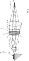
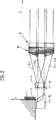
図1は簡略化された側面図であって、この紙面に垂直な座標方向(X軸)に相前後して配置された複数のエミッタ又はエミッタ群を備え及び個々のエミッタの光線を共通の焦点に集光するための本発明による光学装置の一例を備えたレーザダイオードシステムを示す。
【0014】
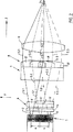
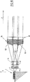
図2は図1のレーザダイオードシステム及びその一部を成す光学装置の平面図、即ち図1の実施例を90度回した状態で示したもので、図1の紙面に垂直なX軸方向に3つのエミッタ又はエミッタ群が連続して備えられた状態を示す。
図3は図2に類似の図であって、レーザダイオードシステムの活性層に平行に、即ちX軸に総計6つのエミッタ又はエミッタ群が備えられた実施例を示す。
【0015】
図4及び図5は図1に類似の図で、本発明の他の可能な実施例を示す。
図6は他の実施例を示す図1に類似の図で、この実施例では活性層に垂直な面において複数列のエミッタ又はエミッタ群が重なり合って配置され、各列のエミッタ又はエミッタ群はこの図の紙面に相前後して配置され、及び全てのエミッタ又はエミッタ群の光線を共通の焦点に集光するための光学装置を示す。
【0016】
図7及び図8は他の可能な実施例を示す図1及び図2に類似の図を示す。
図9、図10及び図11は第1の視準光学装置の点で異なる他の実施例を示す図である。
図12、図13及び図14は本発明の他の可能な実施例を部分的に示す図である。
【0017】
図において、X、Y及びZで、X軸、Y軸及びZ軸で示される互いに垂直な3つの座標方向を示す。
図1及び図2は図示及び説明を簡単にするため全体で3つのエミッタ又はエミッタ群2を有するレーザダイオードチップの型のレーザダイオードシステム1を示し、それらのエミッタ又はエミッタ群はX軸に、これらのエミッタの活性層の方向に予め与えられた距離aの間隔で一列に連続して配置される。
【0018】
個々のエミッタ又はエミッタ群2は上記のように、活性層に垂直な面(図1の紙面)において活性層の面(図2の面)よりかなり強く分散する光線を発する。理解を容易にするため、3つのエミッタ群2の光線のエッジラインを図1及び図2においてそれぞれS1、S2、S3で示す。
エミッタ群2の光線を充分に利用できるようにするため、2つの面において、即ちエミッタ群2の活性層に垂直な平面及び該活性層に平行な平面において可能な限り同じ大きさの焦点径が生じ、即ち可能な限り丸い焦点が得られ、これが例えば点3において図示しないファイバ光学装置に光を供給するために必要な又は少なくとも合理的であるように、これらの光線を共通点3に集光することが必要である。
【0019】
この焦点に集光することは図1及び図2中に同様に示された光学装置によって達成される。これは次に述べる要素からなり、それらの要素はこの光学装置の光学軸の方向にもしくはZ軸の方向にレーザダイオードシステム1から始まる次のリストの順番に互いに接続し、その場合、図示の実施例では焦点3を貫通する光学軸はX軸に垂直な及びエミッタ群の活性層の平面に生じる。即ち、
非球面の円筒面を有する円筒レンズ要素又は円筒レンズ4、
光学軸に垂直な方向に及びエミッタ群2の活性面に、即ちX軸の方向に相前後して配置された複数のプリズム要素6'を有し、その数及び間隔はエミッタ群2の数及びその間隔aに等しい第1のプリズムブロック6、
光学軸に垂直で且つエミッタ群2の活性面に垂直な座標方向、即ちY軸方向に連続して備えられた全体で3つの種々のプリズム要素7'を有する第2のプリズムブロック7、
複数の円筒レンズ要素8'を有し、それらの円筒レンズ要素はそれらの円筒軸がY軸の座標方向に配置され且つY軸に関し3つの面で該面のX軸に重ね合わせに、該面にエミッタ群2の間隔に等しい値で配置される円筒レンズ装置8、
光学軸もしくはZ軸に関し軸対称に配置され及び図示の実施例では両面凸レンズである凸レンズ9、によって構成される。
【0020】
この凸レンズの代りに、他の光学の焦点合わせ装置、例えば多レンズの焦点合わせ装置を備えることもできる。
この光学装置の作用は以下に示すように行なわれる。即ち、活性層に平行な各面及び活性層に垂直な各面でも大きな分散角を有する各エミッタ群2のレーザ光線S1−S3は、その円筒軸線がX軸に配置される円筒レンズ装置4を通して、活性層に垂直な面(Y−Z面)に直ちに数mradの分散まで視準される。このため円筒レンズ装置4は前述のように、非球面の円筒面を有する。視準後の各レーザ光線の測定値は例えば0.5〜1.5mmである。活性層に垂直な各Y−Z面において視準された各エミッタ群のレーザ光線は第1のプリズムブロック6のそれらのエミッタ群のために備えられたプリズム要素6'に入る。
【0021】
個々のプリズム要素6'は活性層に垂直な面において種々の形態でレーザ光線の偏向を起こすように形成され、即ち外側のエミッタ群2のレーザ光線S1はそこに所属のプリズム要素6'を通して或る中心角、例えば図1に選択された形態では10度の角度を上方に偏向され、中間のエミッタ群2のレーザ光線S2はそこに所属のプリズム要素6'を通して偏向されることなく案内され及び他の外側のエミッタ群2のレーザ光線S3は図1に選択された形態では或る角度、即ちこの実施例では光線S1と同じ角度、例えば10度の角度を下方に変更されるように形成される。X軸方向のプリズム要素6'の幅はこの場合、正確にエミッタ群2の間隔aに一致する。
【0022】
Y−Z面で視準され及びX−Z面で分散する偏向された光線S1−S3はさらに大きな第2のプリズムブロック7、もしくは各光線S1−S3のためそこに備えられ及び各エミッタ群2のため区分されて備えられたプリズム要素7'に入る。プリズムブロック6に向き且つY−Z面に垂直なプリズム要素7'の面は光学軸もしくはZ軸に対し傾斜し、もしくはこの軸線に対し、プリズムブロック7内で3つの光線面において互いに平行なレーザ光線S1−S3が生じるような角度で接合する。
【0023】
プリズムブロック6から遠方のプリズムブロック7の側には円筒レンズ装置8が備えられ、例えば光学軸(Z軸)に垂直な面内に在るプリズムブロック7の平らな側面上に上記したシステムにおける個々の半円筒レンズ要素8'が3列に互いにパテで結合されることによって備えられる。各円筒レンズ要素8'はさらに光線S1−S3に割り当てられ且つX−Z面においてこれらの光線S1、S2及びS3の視準を行なうので、各光線は円筒レンズ装置8を過ぎるとX軸及びY軸においても視準され及びそのように視準された光線S1−S3は従来の凸レンズ9によって共通の焦点3に写像され得る。平凸の円筒レンズ要素8'は球面状または非球面状であってもよい。
【0024】
上記の光学装置は3つ以上のエミッタ群を有するエミッタ装置にも用い得ることは理解されよう。この場合、例えばプリズム要素6'の個数、従って3つの光線面で偏向される光線S1−Snの個数が増加され、その場合、各光線面の比較的大きなプリズムブロック7において2又はそれ以上の光線が並んで備えられ及び円筒レンズ装置8は各面に少なくとも2つの円筒レンズ要素8'を有し、該要素8'は各面において、レーザダイオードシステム1におけるエミッタ群の間隔aにプリズムブロック7における光線面の数を乗じたものに等しい間隔をその間に有する。さらに、プリズムブロック6及び7の相応の形態はY軸において3つ以上の光線面を、例えば5つの光線面を積み重ねて備えることもできる。
【0025】
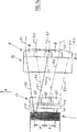
図3は図2に類似の形態の実施例を示すものであって、この例ではレーザダイオードシステム1aは合計6つのエミッタ群2を有し、それらのレーザ光線はプリズムブロック6aを通して次のように偏向される。即ち、プリズムブロック7aの内側で、Y軸方向に重なり合う3つの光線面が生じ、且つそれらの各光線面でX軸の方向に並んで2つの独立の光線が即ち上側の面には光線S1とS1'が、中間面には光線S2とS2'が、及び下側の面には光線S3とS3'が配置されるように偏向される。プリズム要素6'の数はエミッタ群の数と同じである。プリズム要素7'の数は光線面の数と同じである。その上、プリズム要素6'は、或るエミッタ群2の光線が、nをY軸に重ねて配置された光線面の数とすれば、エミッタ群の列においてそのエミッタ群の次のエミッタ群nに相応する光線面に入るその光線と共に偏向されるように形成される。円筒レンズ装置8の代りに図3では円筒レンズ装置8aが用いられ、該装置8aは各光線面に2つの円筒円筒レンズ要素8'を備え、それらの要素は光線面から光線面に、さらにX軸において間隔aで置かれ且つこの軸線において各光線面にnxaの距離を有する。
【0026】
本発明による形態はエミッタ群のレーザ光線を2つの光線面に分配する場合に、特に焦点合わせに関し、異なる光線面にレーザ光線を分配することが予見されない既知の光学装置に対し、著しい改良を達成した。それに関しては次の表1に示す。その表1にはX軸に10mmの長さ、800ミクロンのエミッタ間隔及び400ミクロンのエミッタの幅を有するレーザダイオードシステムの写像特性の比較を、3つの異なる光学装置につき、さらに単に一つの光線面を有する、即ち偏向のない(1−面)装置、図1−図3に関し記載した3つの光線面をもつ(3−面)装置及びY軸に重ね合わせて配置された5つの光線面で偏向が行なわれる(5−面)光学装置につき、示した。
【0027】
レーザダイオードのチップ又はバーには13のエミッタ群が配置される。第1の視準光学装置、即ち円筒レンズ装置4の影響を査定するため、このレンズ装置を通してレーザ光線を伝導した後にY軸に20mradの全分散角を採用した。理想的な間隔はレーザダイオードチップの2つのエミッタ群の光線の重なりの位置を遠ざけることによって予め与えられるので、個々のエミッタ群2の分散角はレーザダイオードシステムもしくはレーザダイオードチップの円筒レンズ装置8もしくは円筒レンズ要素8'の間隔を決定する。X−Z面における分散角は計算のため10度を採用した。凸レンズ9による焦点合わせのため0.2の数値上の開きが基礎とされ、これは石英ファイバのファイバ結合のための通常の数値上の開きに相当する。その開き角度は23度である。
【0028】
【表1】

この表は、単一の平面を有する光学装置の場合、「緩動軸光学」の、即ちX軸で視準を生じさせる光学の非常に小さな焦点距離に基づいて、該軸において焦点の最大の広がりが在ることを証明している。他方ではエミッタ群の光線は本発明が予見するように複数の光線面に分配されるので、かなり小さな焦点径が特にまたX軸において達成され、相応の数の光線面が在る場合、X軸及びY軸においてほぼ丸い焦点3、即ち同じ焦点径を得ることができる。
【0030】
本発明ではまた、円筒レンズ装置8もしくは8aに入るまでに、各場合に種々の光線面への光線の分離が完了するので、この装置にとって形態(2又はそれ以上の面)に依り焦点距離として10〜20mmが得られることは重要である。レンズの高さ1mm、各プリズム要素6'の出口側と各プリズム要素7'の入口側との間の間隔5mm、これらの要素の屈折率1.5の場合、3つの光線面を使用することにより約20度のプリズム要素6'の正及び負の傾斜面の傾斜角が得られる。この角度は例えばプリズム要素6'と7'の屈折率を高めることにより、レンズ要素8'のレンズ高さを小さくすることにより及びプリズムブロック6と7の間の間隔を大きくすることによって小さくすることができる。
【0031】
図4は他の可能な実施例を示すもので、この形態が図1の実施例と異なる点は分離されたプリズムブロック6及び7の代りに結合形のプリズムブロック10を用いた点であり、該ブロック10は円筒レンズ要素4に向いた側にプリズム要素6'を備え及び円筒レンズ装置8bに向いた出口側にプリズム要素7'もしくはそれに相応のプリズム面を有する。円筒レンズ装置8bは円筒レンズ装置8又は8aに相当し、このため光学的に中立の円板11からなるプリズムブロック10から離れており、該円板に円筒レンズ要素8'が接着される。
【0032】
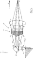
図5は他の実施例を示すものであって、この例はプリズムブロック6もしくは透明な要素の代りに反射要素12を用いた点で図1の実施例とは異なり、該反射要素は各エミッタ群2のため種々の反射面12'を有し、種々の光線面において光線S1−S3もしくはS1−S3'の上記の偏向を達成する。
図6は複数のレーザダイオードシステム1又は1aがY軸において重ね合わせに配置された実施例を示し、この場合各レーザダイオードシステム1又は1aはX軸において多数のエミッタ又はエミッタ群2を有する。
【0033】
エミッタ群の個々の光線を種々の光線面に、即ち各レーザダイオードシステムのため図6に選択された形態では3つの光線面に分配し及びX軸とY軸において視準するため、各レーザダイオードシステム1又は1aには円筒レンズ装置8を備えたプリズムブロック6及び7が配置される。この実施例では凸レンズ9の代りに全てのレーザダイオードシステム1もしくは1aに共通な凸レンズ13が設置され、該凸レンズによってレーザ光線は共通の焦点14に集められ、もしくは写像される。
【0034】
図7及び図8は次の点で図1及び図2の実施例とは本質的に異なる実施例を示し、即ち円筒レンズ装置4に向いたプリズムブロック6の側にプリズム要素6'の傾斜面が在り、及びプリズムブロック7の代りにプリズムブロック15が備えられ、該ブロックはY軸の方向に置かれる3つの光線面を得るため3つのプリズム要素15'を備え、それらのプリズム要素の両方の外側のプリズム面はX−Y平面に対し或る角度で交わり及び中間のプリズム要素15'は該平面に平行である。
【0035】
プリズムブロック6に面する中間のプリズム要素15'はプリズムブロック15のくぼみ15"の底部からなり、該底部によりプリズムブロック15を通る光路の長さが中央において短くなっている。従って、この形態においてレーザ光線S1−S3の相差又は走時差の補償が行なわれるので、全ての光線を面に正確に焦点合わせすることが可能になる。
【0036】
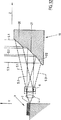
図9は第1の視準光学装置として円筒レンズ装置4の代りに鏡16を用いる点で図7及び図8の実施例と本質的に異なる実施例を示すもので、該鏡は一つの軸線、即ちX軸に平行な軸線のまわりに凹状にわん曲し及びX軸方向に延びる。この鏡によって同時にレーザ光線S1−S3の90度の偏向が行なわれるので、この実施例ではレーザダイオードシステム1のエミッタ又はエミッタ群2はX−Y面に配置される。この場合の特別な利益は共通のX−Y面に複数列のエミッタ群がある場合に特に、全てのエミッタ群に共通の冷却装置を設けることができるので冷却用の手段を著しく単純化することができる。複数列のエミッタ群を備えるそのようなレーザダイオードシステムのエミッタ群の列はY軸に重ね合わせに設置され、しかもその間に置かれ且つエミッタ群を支持する基礎の一部でもあり得る鏡16が備えられる。
【0037】
図10及び図11に示す実施例は図7及び図8の実施例に対し、第1の視準光学装置として円筒レンズ装置4を用いる代りに、自筆的に(ホログラフィックに)作用し、レーザ光線S1−S3を透光する光学要素17(図10)もしくは反射要素18(図11)を備えることで本質的に異なる。
【0038】
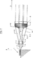
図12は他の可能な実施例を部分的に示すものであって、この実施例が図1の実施例と本質的に異なる点はプリズムブロック7の代りに反射装置又は鏡19を備えることであり、該装置はプリズムブロック6を通して種々の角度で偏向された各レーザ光線S1−S3のための反射面又は鏡20−22を有する。これらの面はそれぞれ図12の紙面に垂直に延びるX軸に平行もしくはY−Z面に垂直な面内に在り且つX−Y面に種々の角度で交わり、しかも光線S2のための鏡面21の角度は鏡20の角度より大きく、及び鏡面22の角度は鏡面21の角度より大きい。さらに鏡面20−21の傾斜は、この実施例ではそれらの反射された光線がY軸の方向ではなくZ軸の方向に相対して設けられる種々の光線面に在って互いに平行になるように、選定される。反射された平行な光線S1−S3はこの図には示されていないが図1に対し約90度回して設置される円筒レンズ装置8に導入される。
【0039】
図13と図14は図1と図2に類似する図であるが、本発明のさらに他の可能な実施例を示し、次の点で図1及び図2の実施例と本質的に異なる。即ち、2つの偏向装置を構成するプリズムブロック6及び7の代りに、もしくはプリズム要素6'及び7'の代りに、回折光学要素、即ち光屈折要素が、しかもこの実施例では伝導装置23と24が備えられることであり、これらの装置はX軸の方向に、この座標方向に備えられた3つのエミッタ群2もしくはその光線S1−S3のため、さらに備えられた3つの光回折区域23'もしくは24'を有し、該装置23において光線はさらにZ軸に対し種々の角度で偏向され、次いで装置24においてY軸方向に相対して平行な光線になるように偏向される。
【0040】
これらの装置23と24もしくは区域23'と24'はそれぞれ光の回折に適した格子状の構造物である。
レーザ光線S1−S3の向きを変えるため、非伝導の、即ち光を回折する反射する要素、さらには反射要素12又は19に類似の要素も考えられ、その場合、そこに置かれる反射面又は鏡面を、光の回折により反射作用する相応の構造物で置き換えられる。
【0041】
図7−図14には凸レンズ9もしくは14は示されていない。これらの実施例でも視準された光線が共通の焦点3もしくは14に写像される際はそれぞれ凸レンズが使用される。明らかなように、図7ないし図14の実施例でも原則として複数列のエミッタ又はエミッタ群を備えることは可能である。
本発明はこれまで実施例に関し記載したが、本発明に基づく発明思想から離れることなく他の変形及び変態が可能なことが理解されよう。従って、それぞれ群を形成する複数のエミッタの代りに、同じ方法で単一のエミッタ又はそれぞれ下部の群に形成される複数の群を扱い、その場合、各下部の群が多数のエミッタを備えるようにすることも可能である。
【図面の簡単な説明】
【0042】
【図1】本発明による光学装置の一例を備えたレーザダイオードシステムを示す簡略化された側面図である。
【図2】図1のレーザダイオードシステム及びその一部を成す光学装置の平面図である。
【図3】図2に類似の図である。
【図4】本発明の他の実施例を示す図1に類似の図である。
【図5】同じく本発明の他の実施例を示す図1に類似の図である。
【図6】同じく本発明の他の実施例を示す図1に類似の図である。
【図7】本発明の他の実施例を示す図1及び図2に類似の図である。
【図8】本発明の他の実施例を示す図1及び図2に類似の図である。
【図9】第1の視準光学装置の点で異なる他の実施例を示す図である。
【図10】同じく第1の視準光学装置の点で異なる他の実施例を示す図である。
【図11】同じく第1の視準光学装置の点で異なる他の実施例を示す図である。
【図12】本発明の他の可能な実施例を部分的に示す図である。
【図13】同じく本発明の他の可能な実施例を部分的に示す図である。
【図14】同じく本発明の他の可能な実施例を部分的に示す図である。
【符号の説明】
【0043】
1、1a レーザダイオードシステム
2 エミッタ群
3 焦点
4 円筒レンズ装置(視準光学装置)
6、7、6a、7a プリズムブロック(偏向手段)
6'、7' プリズム要素(偏向手段)
8、8a、8b 円筒レンズ装置(視準光学装置)
8' 円筒レンズ要素(視準光学装置)
9 凸レンズ(視準光学装置)
10 プリズムブロック(偏向手段)
11 円板
12 反射要素(偏向手段)
12' 反射面
13 凸レンズ(視準光学装置)
14 焦点
15 プリズムブロック(偏向手段)
15' プリズム要素(偏向手段)
15" くぼみ
16 鏡(偏向手段)
17、18 偏向光学装置(偏向手段)
19 鏡(偏向手段)
20−22 鏡面(偏向手段)
23、24 光回折装置(偏向手段)
23'、24' 光回折区域(偏向手段) 【Technical field】
[0001]
The present invention relates to a device for collimating light rays from a photoelectric element in two coordinate directions perpendicular to each other and perpendicular to the optical axis and then condensing at a high light density at the focal point, in particular according to
[Background]
[0002]
Semiconductor diode laser beamGreatly dispersedUnlike other conventional laser beam sources having a diameter of several millimeters with a slight beam dispersion in the range of several mrad, the laser beam has a dispersion of 1000 mrad or more. It is already known.
[0003]
There is a need for micro-optics or optical devices that collimate and focus in order to be able to use semiconductor diode laser beams. In this case, it should be taken into account that the semiconductor laser diode usually comprises a plurality of emitters or groups of emitters in a row and at intervals of several hundred microns. When designing optical devices or micro-optical instruments, the laser beam used for each emitter or group of emitters is optical because the lenses used must be placed closely on the current semiconductor diode laser or corresponding laser device or on the chip. It must be taken into account that light does not overlap before entering the device and that considerable beam loss is caused by light scattering based on projection angles that are otherwise unacceptable or not appropriate. Furthermore, it should be considered when designing an optical device that the dispersion angle in the plane perpendicular to the active layer (Fast-Axis) is larger than the dispersion angle in the plane of the active layer (Slow-Axis) in the semiconductor laser diode.
[0004]
It is already known to collimate a laser beam dispersed by an emitter or a group of emitters with two cylindrical lenses arranged one after the other with respect to the optical axis, in which case a fast axis (Fast- Axis), that is, collimation in the direction of the axis perpendicular to the surface of the active layer and collimation in the direction of the slow axis with the second cylindrical lens further away from the laser diode device.
[0005]
In this case, in particular also an optical device (US Pat. No. 3,396,344) is known, in which a plurality of laser diodes or emitters or emitter groups are arranged in at least two rows, each row being in the first coordinate direction. A plurality of emitters or groups of emitters on the surface of the active layer and the two columns are in a second coordinate direction perpendicular to the active layerArrangedPlaced. A first cylindrical lens is provided in each column as a collimating optical device for collimating each light ray and collimating in the second coordinate direction (fast axis). The cylindrical lens device forming the second collimating optical device for collimation in the first coordinate direction (slow axis) comprises a plurality of cylindrical lens elements, each of which has two lens elements. Installed to act for the laser beams of the superimposed emitters, juxtaposed in two adjacent rows and directly adjacent.
[0006]
The cylindrical lens elements adjacent to each other of the first collimating optical device, in particular the second collimating optical device, for the intended collimation, are also determined with a determined lens height and a determined radius of curvature. The space between individual emitters or groups of emitters is relatively large in each row. This means that the chip density forming the laser diode device is relatively small, even though higher packing density and therefore higher power is possible, even from chip technology or considering the development of powerful coolers Means that.
[0007]
Furthermore, with known optical devices, and in particular with a large number of emitters or groups of emitters in each row, focusing or mapping of the laser beam at the focal point occurs, the focal diameter in the first coordinate direction being larger than that in the second coordinate direction. , There is a drawback.
DISCLOSURE OF THE INVENTION
[Problems to be solved by the invention]
[0008]
The object of the present invention is to eliminate the above drawbacks with a relatively simple structure, and in particular to reduce the spacing between the emitters or groups of emitters in a row of emitters or groups of emitters, and thus of the chips forming the laser diode device. It is to provide an optical device that can significantly increase the housing density and enable high output.
[Means for Solving the Problems]
[0009]
In order to solve the above problems, an optical device according to the characterizing portion of
A feature of the present invention is that the laser beams of adjacent emitters or groups of emitters in a row are deflected as follows. That is, the various collimated light planes after the collimated laser beam of an adjacent emitter or group of emitters has passed through the second collimating optical device(Surface formed by edge lines indicating the spread of light rays)In other words, for example, the light beams are deflected so as to be parallel to each other in the light beam plane disposed in the axial direction perpendicular to the surface of the active layer. In these planes, the laser beam is in the slow axis, i.e.Active layer is locatedSince it is collimated in the first coordinate direction, the collimating elements used for this, for example the cylindrical lens elements of the second collimating optical device, are arranged in these ray planes and installed in various ray planes. Collimating elements can be superimposed. As a result, the spacing between individual emitters or emitter groups can be reduced and a high accommodation density can be realized. If the number of light planes used is n and the distance between adjacent emitters or groups of emitters is a, the collimating element spacing nxa in each light plane occurs in the second collimating optical device, ie By reducing the distance a and increasing the accommodation density, the collimating element distance required for structural reasons on each light plane is realized.
[0010]
"Non-centered collimating optics" or "cylindrical collimating optics" should be understood in the sense of the present invention as optics that generally produce the same or similar mapping as cylindrical optics or cylindrical lenses.
Laser beams collimated in two planes can be mapped through a focus optic to a common spatial area or focus.
【The invention's effect】
[0011]
A particular advantage of the present invention is that it allows the use of a laser diode system having a high housing density and high power while retaining a relatively simple structure, without loss due to light scattering. Therefore, the highest output of the semiconductor diode laser is also realized by the use of high power cooler technology provided for processing.
[0012]
Further, the present invention can form a focal shape in a desired manner by selecting an appropriate number of ray planes when the number of emitters or emitter groups in a row is predetermined, for example, circular or circular. There is an advantage that a focal point having a shape close to that can be formed.
In a simple embodiment of the invention, the emitters or emitter groups are arranged in only one row. In the present invention, it is also possible to arrange such emitters or emitter groups in a plurality of rows in a coordinate direction perpendicular to the plane of the active layer.
BEST MODE FOR CARRYING OUT THE INVENTION
[0013]
The advanced forms of the invention are subject to the dependent claims.
Next, the present invention will be described in detail by way of examples with reference to the drawings.
FIG.Is a simplified side view, comprising a plurality of emitters or groups of emitters arranged one after the other in a coordinate direction (X axis) perpendicular to the plane of the drawing, and collecting the rays of the individual emitters at a common focus. 1 shows a laser diode system with an example of an optical device according to the invention for illuminating.
[0014]
FIG.IsFIG.A plan view of the laser diode system and the optical device forming part thereof;FIG.Is shown in a state rotated 90 degrees,FIG.3 shows a state in which three emitters or emitter groups are continuously provided in the X-axis direction perpendicular to the paper surface.
FIG.IsFIG.Figure 6 shows an embodiment with a total of six emitters or groups of emitters parallel to the active layer of the laser diode system, i.e. in the X axis.
[0015]
FIG.as well asFIG.IsFIG.Figure 6 shows another possible embodiment of the invention in a similar figure.
FIG.Shows another embodimentFIG.In this embodiment, in this embodiment, a plurality of rows of emitters or emitter groups are arranged to overlap each other in a plane perpendicular to the active layer, and the emitters or emitter groups of each row are arranged one after the other on the paper surface of this figure, And an optical device for condensing the rays of all emitters or groups of emitters at a common focal point.
[0016]
FIG.as well asFIG.Shows other possible embodimentsFIG.as well asFIG.A similar figure is shown.
FIG.,FIG.as well asFIG.FIG. 10 is a diagram showing another embodiment which is different from the first collimating optical device.
FIG.,FIG.as well asFIG.FIG. 4 partially illustrates another possible embodiment of the present invention.
[0017]
In the figure, X, Y, and Z indicate three coordinate directions that are perpendicular to each other and that are indicated by the X, Y, and Z axes.
FIG.as well asFIG.Shows a
[0018]
Each emitter or
In order to make full use of the rays of the
[0019]
Focusing on this focusFIG.as well asFIG.This is achieved by the optical device shown in the same way. This consists of the following elements, which are connected to each other in the order of the following list starting from the
A cylindrical lens element or
It has a plurality of
A
A plurality of
It is arranged symmetrically with respect to the optical axis or the Z axis, and is constituted by a
[0020]
Instead of the convex lens, another optical focusing device, for example, a multi-lens focusing device may be provided.
The operation of this optical device is performed as follows. That is, the laser beams S1-S3 of each
[0021]
The individual prism elements 6 'are formed to cause the deflection of the laser beam in various forms in the plane perpendicular to the active layer, ie the laser beam S1 of the
[0022]
The deflected rays S1-S3 collimated in the YZ plane and dispersed in the XZ plane are provided there for a larger
[0023]
On the side of the
[0024]
It will be appreciated that the optical device described above can also be used with emitter devices having more than two emitter groups. In this case, for example, the number of prism elements 6 'and thus the number of rays S1-Sn deflected by three ray planes is increased, in which case two or more rays in a relatively
[0025]
FIG.IsFIG.In this example, the
[0026]
The configuration according to the invention achieves a significant improvement when distributing the laser beam of the emitter group to two beam planes, especially with respect to focusing, over known optical devices where it is not foreseen to distribute the laser beam to different beam planes. did. In that regard the following table1Shown in The table1Compare the mapping characteristics of laser diode systems with a length of 10 mm on the X-axis, an emitter spacing of 800 microns and an emitter width of 400 microns, with just one ray plane for three different optical devices, A non-deflection (1-plane) device,FIG.−FIG.The three-plane (3-plane) device described with reference to FIG. 5 and the five-plane optical device in which the deflection is performed with five ray planes arranged superimposed on the Y axis are shown.
[0027]
Thirteen emitter groups are arranged on the laser diode chip or bar. In order to assess the influence of the first collimating optical device, ie the
[0028]
[Table 1]
This table shows that in the case of an optical device with a single plane, the maximum focal length in that axis is based on the very small focal length of “slow axis optics”, ie the optics that cause collimation in the X axis. Prove that there is a spread. On the other hand, the rays of the emitter group are distributed over a plurality of ray planes as the present invention predicts, so that a fairly small focal diameter is also achieved, especially in the X axis, where there is a corresponding number of ray planes, the X axis. And a substantially round
[0030]
The present invention also completes the separation of the rays into the various ray planes in each case before entering the
[0031]
FIG.Shows other possible embodiments, this formFIG.The difference from the first embodiment is that instead of the separated prism blocks 6 and 7, a combined
[0032]
FIG.Shows another embodiment, and this example uses a
FIG.Shows an embodiment in which a plurality of
[0033]
The individual beams of the emitter group are on different beam planes, ie for each laser diode systemFIG.In the form selected in the above, each
[0034]
FIG.as well asFIG.IsFIG.as well asFIG.An embodiment which is essentially different from the above embodiment is shown, that is, the inclined surface of the
[0035]
The
[0036]
FIG.Is that a
[0037]
FIG.as well asFIG.Examples shown inFIG.as well asFIG.For this embodiment, instead of using the
[0038]
FIG.Is a partial illustration of another possible embodiment,FIG.In essence, this embodiment is provided with a reflector or
[0039]
FIG.WhenFIG.IsFIG.WhenFIG.Is a diagram similar to, but illustrates yet another possible embodiment of the present invention in the following respects:FIG.as well asFIG.This embodiment is essentially different from the first embodiment. That is, instead of the prism blocks 6 and 7 constituting the two deflecting devices, or instead of the prism elements 6 'and 7', a diffractive optical element, i.e. a photorefractive element, and in this embodiment the conducting
[0040]
These
In order to change the direction of the laser beams S1-S3, non-conducting, i.e. reflecting elements that diffract light, and also elements similar to the reflecting
[0041]
FIG.−FIG.No
While the invention has been described with reference to exemplary embodiments, it will be understood that other variations and modifications can be made without departing from the inventive concept based on the invention. Thus, instead of a plurality of emitters each forming a group, a single emitter or a plurality of groups each formed in a lower group are treated in the same way, with each lower group comprising a number of emitters. It is also possible to make it.
[Brief description of the drawings]
[0042]
FIG. 1 is a simplified side view illustrating a laser diode system with an example of an optical device according to the present invention.
[Figure 2]FIG. 2 is a plan view of the laser diode system of FIG. 1 and an optical device forming a part thereof.
[Fig. 3]FIG. 3 is a view similar to FIG. 2.
[Fig. 4]It is a figure similar to FIG. 1 which shows the other Example of this invention.
[Figure 5]It is a figure similar to FIG. 1 which similarly shows the other Example of this invention.
[Fig. 6]It is a figure similar to FIG. 1 which similarly shows the other Example of this invention.
[Fig. 7]It is a figure similar to FIG.1 and FIG.2 which shows the other Example of this invention.
[Fig. 8]It is a figure similar to FIG.1 and FIG.2 which shows the other Example of this invention.
FIG. 9It is a figure which shows the other Example different in the point of a 1st collimation optical apparatus.
FIG. 10It is a figure which similarly shows the other Example different in the point of a 1st collimation optical apparatus.
FIG. 11It is a figure which similarly shows the other Example different in the point of a 1st collimation optical apparatus.
FIG.FIG. 6 partially illustrates another possible embodiment of the present invention.
FIG. 13FIG. 6 also partially shows another possible embodiment of the invention.
FIG. 14FIG. 6 also partially shows another possible embodiment of the invention.
[Explanation of symbols]
[0043]
1, 1a Laser diode system
2 Emitter group
3 Focus
4 Cylindrical lens device(Collimation optics)
6, 7, 6a, 7a Prism block(Deflection means)
6 ', 7' prism element(Deflection means)
8, 8a, 8b Cylindrical lens device(Collimation optics)
8 'cylindrical lens element(Collimation optics)
9 Convex lens(Collimation optics)
10 Prism block(Deflection means)
11 disc
12 Reflective elements(Deflection means)
12 'Reflective surface
13 Convex lens(Collimation optics)
14 Focus
15 Prism block(Deflection means)
15 'prism element(Deflection means)
15 "indentation
16 mirrors(Deflection means)
17, 18 Deflection optical device(Deflection means)
19 mirror(Deflection means)
20-22 Mirror surface(Deflection means)
23, 24 Optical diffraction device(Deflection means)
23 ', 24' light diffraction area(Deflection means)
Claims (20)
前記活性層が位置する第1の座標方向(X軸)に垂直な第1の面(Y−Z面)において、前記エミッタ又はエミッタ群(2)の複数のレーザ光線(S1−S3、S1'−S3')の視準を行なう円筒状に作用する第1の視準光学装置(4、16、17、18)と、
前記第1の面(Y−Z面)に垂直で第2の座標方向(Y軸)に垂直な第2の面(X−Z面)において前記エミッタ又はエミッタ群(2)のレーザ光線(S1−S3、S1'−S3')の視準を行なう円筒状に作用する第2の視準光学装置(8、8a、8b)と、
前記円筒状に作用する第2の光学視準装置(8、8a、8b)を通過した後に、前記各列のエミッタ又はエミッタ群(2)の視準されたレーザ光線(S1−S3、S1'−S3')が、前記第2の座標方向(Y軸)に互いにずらされた種々の光線面内に位置して互いに平行になるよう、前記第1の面(Y−Z面)において前記エミッタ又はエミッタ群(2)のレーザ光線(S1−S3、S1'−S3')を偏向させるための偏向手段(6、6a、7、7a、7b、12、15、19)を備えたことを特徴とするレーザダイオードシステム用の光学装置。A plurality of emitters or emitter groups (2) are arranged in a row or a plurality of rows, and the emitters or emitter groups (2) in each row are arranged in advance in one axial direction with their active layers positioned in one common plane. With respect to the laser diode system (1, 1a) arranged at a predetermined interval (a), the laser beams (S1-S3, S1′-S3 ′) of the plurality of emitters or emitter groups (2) are viewed. Equivalent optical device,
On a first surface (YZ plane) perpendicular to the first coordinate direction (X axis) where the active layer is located, a plurality of laser beams (S1-S3, S1 ′) of the emitter or emitter group (2) A first collimating optical device (4, 16, 17, 18) acting in a cylindrical shape for collimating -S3 ′);
A laser beam (S1) of the emitter or emitter group (2) on a second surface (XZ plane) perpendicular to the first surface (YZ plane) and perpendicular to the second coordinate direction (Y axis) A second collimating optical device (8, 8a, 8b) acting in a cylindrical shape for collimating -S3, S1'-S3 ');
After passing through the cylindrical second optical collimation device (8, 8a, 8b), collimated laser beams (S1-S3, S1 ′) of the emitters or emitter groups (2) in each row -S3 ') in the first plane (Y-Z plane) such that the emitters are positioned in parallel to each other in the various ray planes shifted from each other in the second coordinate direction (Y-axis). Alternatively, it is provided with deflection means (6, 6a, 7, 7a, 7b, 12, 15, 19) for deflecting the laser beam (S1-S3, S1′-S3 ′) of the emitter group (2). An optical device for a laser diode system.
Applications Claiming Priority (5)
| Application Number | Priority Date | Filing Date | Title |
|---|---|---|---|
| DE19500513.9 | 1995-01-11 | ||
| DE19500513A DE19500513C1 (en) | 1995-01-11 | 1995-01-11 | Optical arrangement for chip formed multiple semiconductor laser array |
| DE19544488A DE19544488A1 (en) | 1995-01-11 | 1995-11-29 | Optical arrangement for use in a laser diode arrangement |
| DE19544488.4 | 1995-11-29 | ||
| PCT/DE1995/001813 WO1996021877A1 (en) | 1995-01-11 | 1995-12-19 | Optical arrangement for use in a laser diode system |
Publications (2)
| Publication Number | Publication Date |
|---|---|
| JPH10508122A JPH10508122A (en) | 1998-08-04 |
| JP4025366B2 true JP4025366B2 (en) | 2007-12-19 |
Family
ID=26011522
Family Applications (1)
| Application Number | Title | Priority Date | Filing Date |
|---|---|---|---|
| JP52135996A Expired - Fee Related JP4025366B2 (en) | 1995-01-11 | 1995-12-19 | Optical device for laser diode systems |
Country Status (9)
| Country | Link |
|---|---|
| US (1) | US5808803A (en) |
| EP (1) | EP0803075B1 (en) |
| JP (1) | JP4025366B2 (en) |
| AU (1) | AU4326196A (en) |
| CA (1) | CA2210192A1 (en) |
| DE (1) | DE59510499D1 (en) |
| DK (1) | DK0803075T3 (en) |
| ES (1) | ES2188681T3 (en) |
| WO (1) | WO1996021877A1 (en) |
Families Citing this family (42)
| Publication number | Priority date | Publication date | Assignee | Title |
|---|---|---|---|---|
| US5940998A (en) * | 1996-09-06 | 1999-08-24 | Brauer; William R. | Illuminating apparatus for use with medical diagnostic imaging film |
| US5986794A (en) * | 1997-02-01 | 1999-11-16 | Laserline Gesellschaft Fur Entwicklung Und Vertrieb Von Diodenlasern Mbh | Laser optics and diode laser |
| US6392813B1 (en) * | 1997-11-05 | 2002-05-21 | Patrick J. Reardon | Integrated molded plastic optical system for a laser diode collimating and aberration correction configuration |
| DE19800590B4 (en) * | 1998-01-09 | 2005-12-01 | Jenoptik Ag | Optical arrangement for balancing the radiation of one or more superimposed high-power diode lasers |
| US6075912A (en) * | 1998-03-17 | 2000-06-13 | Polaroid Corporation | Apparatus for coupling radiation beams into an optical waveguide |
| US6324320B1 (en) * | 1998-03-17 | 2001-11-27 | Polaroid Corporation | Optical apparatus for producing a high-brightness multi-laser radiation source |
| DE19839902C1 (en) * | 1998-09-02 | 2000-05-25 | Laserline Ges Fuer Entwicklung | Optical arrangement for use in a laser diode arrangement and diode laser |
| US6377599B1 (en) * | 1999-01-12 | 2002-04-23 | Iridex Corporation | Focusability enhancing optic for a laser diode |
| US6819646B1 (en) * | 1999-01-19 | 2004-11-16 | Matsushita Electric Industrial Co., Ltd. | Optical pickup, optical information recording/reproducing apparatus using the same, and phase variable wave plate used in the pickup and the apparatus |
| ES2184703T3 (en) | 1999-03-31 | 2003-04-16 | Fraunhofer Ges Forschung | OPTICAL DSIPOSITIVE TO MAKE THE RADIATIONS OF BIDIMENSIONAL NETWORKS OF LASER DIODES SIMETRIC. |
| ITMI991271A1 (en) * | 1999-06-08 | 2000-12-08 | Bright Solutions Soluzioni Las | METHOD AND DEVICE TO CONDITION THE LIGHT EMISSION OF A LASER DIODE SET |
| US6400513B1 (en) * | 2000-03-15 | 2002-06-04 | Quantum Devices, Inc. | Optical beam coupling of multiple wavelengths into an output channel using spatial wavefront segmentation |
| DE10016377B4 (en) * | 2000-04-04 | 2009-01-08 | Leica Microsystems Cms Gmbh | Device for combining light |
| EP1150097A1 (en) * | 2000-04-26 | 2001-10-31 | Leica Geosystems AG | Optical rangefinder |
| US6451152B1 (en) | 2000-05-24 | 2002-09-17 | The Boeing Company | Method for heating and controlling temperature of composite material during automated placement |
| EP1215523A3 (en) * | 2000-12-16 | 2004-05-26 | Hentze-Lissotschenko Patentverwaltungs GmbH & Co.KG | Radiation system with beam transformation for generating modulated radiation |
| JP4129233B2 (en) * | 2001-10-17 | 2008-08-06 | ライカ ジオシステムズ アクチエンゲゼルシャフト | Optical distance measuring device |
| FI116010B (en) | 2002-05-22 | 2005-08-31 | Cavitar Oy | Method and laser device for producing high optical power density |
| US20030233580A1 (en) * | 2002-05-29 | 2003-12-18 | Keeler James D. | Authorization and authentication of user access to a distributed network communication system with roaming features |
| KR100474430B1 (en) * | 2002-12-30 | 2005-03-10 | 삼성전자주식회사 | Multi-beam laser scanning unit |
| CA2531122A1 (en) * | 2003-07-03 | 2005-02-10 | Pd-Ld, Inc. | Use of volume bragg gratings for the conditioning of laser emission characteristics |
| US20060221459A1 (en) * | 2005-04-01 | 2006-10-05 | Sagan Stephen F | Optical system for projecting a line of illumination from an array of lasers |
| CN101473259A (en) * | 2006-06-16 | 2009-07-01 | 皇家飞利浦电子股份有限公司 | Light collimation and mixing of remote light sources |
| US7515346B2 (en) | 2006-07-18 | 2009-04-07 | Coherent, Inc. | High power and high brightness diode-laser array for material processing applications |
| DE102009010693A1 (en) * | 2009-02-26 | 2010-09-02 | Limo Patentverwaltung Gmbh & Co. Kg | Device for homogenizing laser radiation |
| GB201107948D0 (en) * | 2011-05-12 | 2011-06-22 | Powerphotonic Ltd | Multi-wavelength diode laser array |
| US10971896B2 (en) | 2013-04-29 | 2021-04-06 | Nuburu, Inc. | Applications, methods and systems for a laser deliver addressable array |
| US10562132B2 (en) | 2013-04-29 | 2020-02-18 | Nuburu, Inc. | Applications, methods and systems for materials processing with visible raman laser |
| US11646549B2 (en) | 2014-08-27 | 2023-05-09 | Nuburu, Inc. | Multi kW class blue laser system |
| CN107045197B (en) * | 2016-02-05 | 2021-09-17 | 苏州旭创科技有限公司 | Optical path control system and optical module |
| EP3422495A4 (en) * | 2016-02-22 | 2019-03-20 | Mitsubishi Electric Corporation | Laser light source device and method for manufacturing laser light source device |
| WO2017189982A1 (en) | 2016-04-29 | 2017-11-02 | Nuburu, Inc. | Visible laser additive manufacturing |
| US11612957B2 (en) * | 2016-04-29 | 2023-03-28 | Nuburu, Inc. | Methods and systems for welding copper and other metals using blue lasers |
| US20220072659A1 (en) * | 2016-04-29 | 2022-03-10 | Nuburu, Inc. | Methods and Systems for Reducing Hazardous Byproduct from Welding Metals Using Lasers |
| JPWO2018037663A1 (en) * | 2016-08-26 | 2019-06-20 | パナソニックIpマネジメント株式会社 | Laser module |
| JP6911153B2 (en) | 2017-01-31 | 2021-07-28 | ヌブル インク | Methods and systems for welding copper using a blue laser |
| WO2018195510A1 (en) | 2017-04-21 | 2018-10-25 | Nuburu, Inc. | Multi-clad optical fiber |
| US10969560B2 (en) | 2017-05-04 | 2021-04-06 | Lightpath Technologies, Inc. | Integrated optical assembly and manufacturing the same |
| CN110999000B (en) | 2017-06-13 | 2021-10-08 | 努布鲁有限公司 | High-density wavelength beam combined laser system |
| WO2020107030A1 (en) | 2018-11-23 | 2020-05-28 | Nuburu, Inc | Multi-wavelength visible laser source |
| CA3127651A1 (en) | 2019-02-02 | 2020-08-06 | Nuburu, Inc. | High reliability, high power, high brightness blue laser diode systems and methods of making the same |
| WO2024075595A1 (en) * | 2022-10-05 | 2024-04-11 | ヌヴォトンテクノロジージャパン株式会社 | Semiconductor laser device |
Family Cites Families (9)
| Publication number | Priority date | Publication date | Assignee | Title |
|---|---|---|---|---|
| GB1040792A (en) * | 1964-02-24 | 1966-09-01 | Nat Res Dev | Optical systems for lasers |
| JPS58192015A (en) * | 1982-05-04 | 1983-11-09 | Toshiba Corp | Plural luminous flux scanner |
| US4530574A (en) * | 1982-07-28 | 1985-07-23 | Xerox Corporation | Beam collimation and focusing of multi-emitter or broad emitter lasers |
| EP0312652B1 (en) * | 1987-10-19 | 1993-09-01 | Hitachi, Ltd. | Optical device with phase-locked diodelaser array |
| JPH02153328A (en) * | 1988-12-05 | 1990-06-13 | Sumitomo Electric Ind Ltd | Light source device |
| US5216562A (en) * | 1990-09-25 | 1993-06-01 | International Business Machines Corporation | Multi-beam optical recording system and method |
| CH682698A5 (en) * | 1990-11-01 | 1993-10-29 | Fisba Optik Ag Bystronic Laser | Method in which several, arranged in one or more rows of radiation sources are imaged and apparatus therefor. |
| JPH04255280A (en) * | 1991-02-07 | 1992-09-10 | Nippon Steel Corp | Semiconductor laser excitation solid-state laser device |
| US5453814A (en) * | 1994-04-13 | 1995-09-26 | Nikon Precision Inc. | Illumination source and method for microlithography |
-
1995
- 1995-12-19 EP EP95942017A patent/EP0803075B1/en not_active Expired - Lifetime
- 1995-12-19 CA CA002210192A patent/CA2210192A1/en not_active Abandoned
- 1995-12-19 JP JP52135996A patent/JP4025366B2/en not_active Expired - Fee Related
- 1995-12-19 US US08/860,472 patent/US5808803A/en not_active Expired - Lifetime
- 1995-12-19 WO PCT/DE1995/001813 patent/WO1996021877A1/en active IP Right Grant
- 1995-12-19 ES ES95942017T patent/ES2188681T3/en not_active Expired - Lifetime
- 1995-12-19 DE DE59510499T patent/DE59510499D1/en not_active Expired - Lifetime
- 1995-12-19 AU AU43261/96A patent/AU4326196A/en not_active Abandoned
- 1995-12-19 DK DK95942017T patent/DK0803075T3/en active
Also Published As
| Publication number | Publication date |
|---|---|
| DK0803075T3 (en) | 2003-03-31 |
| EP0803075A1 (en) | 1997-10-29 |
| DE59510499D1 (en) | 2003-01-16 |
| US5808803A (en) | 1998-09-15 |
| AU4326196A (en) | 1996-07-31 |
| JPH10508122A (en) | 1998-08-04 |
| WO1996021877A1 (en) | 1996-07-18 |
| CA2210192A1 (en) | 1996-07-18 |
| EP0803075B1 (en) | 2002-12-04 |
| ES2188681T3 (en) | 2003-07-01 |
Similar Documents
| Publication | Publication Date | Title |
|---|---|---|
| JP4025366B2 (en) | Optical device for laser diode systems | |
| US6337873B1 (en) | Optical arrangement for balancing the beam of one or more high power diode lasers arranged one above another | |
| US7110183B2 (en) | Device for the optical beam transformation of a linear arrangement of several light sources | |
| JP3649737B2 (en) | Beam guidance formation mechanism from linear laser diode array | |
| US5319496A (en) | Optical beam delivery system | |
| US6778732B1 (en) | Generation of high-power, high brightness optical beams by optical cutting and beam-shaping of diode lasers | |
| US6443594B1 (en) | One-piece lens arrays for collimating and focusing light and led light generators using same | |
| US6356395B1 (en) | Light intensity distribution converting device and optical data storage apparatus | |
| US7016393B2 (en) | Apparatus for projecting a line of light from a diode-laser array | |
| US6757106B2 (en) | Optical lens, optical lens unit, stacked type optical lens, optical system and semiconductor laser apparatus | |
| JPH08240793A (en) | Refration ellipse optical face without spherical aberration | |
| US6765725B1 (en) | Fiber pigtailed high power laser diode module with high brightness | |
| US6356380B1 (en) | Apparatus for imaging light from multifaceted laser diodes onto a multichannel spatial light modulator | |
| JPH10510933A (en) | Apparatus for focusing and shaping emitted light of multiple diode laser arrays | |
| US5301249A (en) | Catoptric coupling to an optical fiber | |
| US7035014B2 (en) | Device for collimating light emanating from a laser light source and beam transformer for said arrangement | |
| US4565421A (en) | Plural-beam scanning apparatus | |
| JP2003057588A (en) | Shaping optical system for laser bar layered body and laser light source | |
| KR100288967B1 (en) | Optical system for beam shaping and optical pickup employing the same | |
| CN114296089B (en) | Optical system and laser radar | |
| KR19990024008A (en) | Optical Disc Device | |
| US5452384A (en) | Optical integrated lensed connector for focussing oblique incident light | |
| US6768838B2 (en) | Optical module | |
| CN217606192U (en) | Laser coupling device and semiconductor laser system | |
| JP2004085589A (en) | Module for light source and light source device |
Legal Events
| Date | Code | Title | Description |
|---|---|---|---|
| A131 | Notification of reasons for refusal |
Free format text: JAPANESE INTERMEDIATE CODE: A131 Effective date: 20050809 |
|
| A601 | Written request for extension of time |
Free format text: JAPANESE INTERMEDIATE CODE: A601 Effective date: 20051108 |
|
| A602 | Written permission of extension of time |
Free format text: JAPANESE INTERMEDIATE CODE: A602 Effective date: 20051226 |
|
| A521 | Written amendment |
Free format text: JAPANESE INTERMEDIATE CODE: A523 Effective date: 20060118 |
|
| A131 | Notification of reasons for refusal |
Free format text: JAPANESE INTERMEDIATE CODE: A131 Effective date: 20060801 |
|
| A601 | Written request for extension of time |
Free format text: JAPANESE INTERMEDIATE CODE: A601 Effective date: 20061024 |
|
| A602 | Written permission of extension of time |
Free format text: JAPANESE INTERMEDIATE CODE: A602 Effective date: 20061211 |
|
| A521 | Written amendment |
Free format text: JAPANESE INTERMEDIATE CODE: A523 Effective date: 20070122 |
|
| TRDD | Decision of grant or rejection written | ||
| A01 | Written decision to grant a patent or to grant a registration (utility model) |
Free format text: JAPANESE INTERMEDIATE CODE: A01 Effective date: 20071002 |
|
| A61 | First payment of annual fees (during grant procedure) |
Free format text: JAPANESE INTERMEDIATE CODE: A61 Effective date: 20071005 |
|
| R150 | Certificate of patent or registration of utility model |
Free format text: JAPANESE INTERMEDIATE CODE: R150 |
|
| FPAY | Renewal fee payment (event date is renewal date of database) |
Free format text: PAYMENT UNTIL: 20101012 Year of fee payment: 3 |
|
| FPAY | Renewal fee payment (event date is renewal date of database) |
Free format text: PAYMENT UNTIL: 20101012 Year of fee payment: 3 |
|
| FPAY | Renewal fee payment (event date is renewal date of database) |
Free format text: PAYMENT UNTIL: 20111012 Year of fee payment: 4 |
|
| FPAY | Renewal fee payment (event date is renewal date of database) |
Free format text: PAYMENT UNTIL: 20111012 Year of fee payment: 4 |
|
| FPAY | Renewal fee payment (event date is renewal date of database) |
Free format text: PAYMENT UNTIL: 20121012 Year of fee payment: 5 |
|
| FPAY | Renewal fee payment (event date is renewal date of database) |
Free format text: PAYMENT UNTIL: 20121012 Year of fee payment: 5 |
|
| FPAY | Renewal fee payment (event date is renewal date of database) |
Free format text: PAYMENT UNTIL: 20131012 Year of fee payment: 6 |
|
| LAPS | Cancellation because of no payment of annual fees |