JP4017248B2 - Semiconductor device - Google Patents
Semiconductor device Download PDFInfo
- Publication number
- JP4017248B2 JP4017248B2 JP09869498A JP9869498A JP4017248B2 JP 4017248 B2 JP4017248 B2 JP 4017248B2 JP 09869498 A JP09869498 A JP 09869498A JP 9869498 A JP9869498 A JP 9869498A JP 4017248 B2 JP4017248 B2 JP 4017248B2
- Authority
- JP
- Japan
- Prior art keywords
- voltage
- power supply
- command
- memory
- circuit
- Prior art date
- Legal status (The legal status is an assumption and is not a legal conclusion. Google has not performed a legal analysis and makes no representation as to the accuracy of the status listed.)
- Expired - Lifetime
Links
Images


Classifications
-
- G—PHYSICS
- G11—INFORMATION STORAGE
- G11C—STATIC STORES
- G11C5/00—Details of stores covered by group G11C11/00
- G11C5/06—Arrangements for interconnecting storage elements electrically, e.g. by wiring
- G11C5/063—Voltage and signal distribution in integrated semi-conductor memory access lines, e.g. word-line, bit-line, cross-over resistance, propagation delay
-
- G—PHYSICS
- G11—INFORMATION STORAGE
- G11C—STATIC STORES
- G11C11/00—Digital stores characterised by the use of particular electric or magnetic storage elements; Storage elements therefor
- G11C11/21—Digital stores characterised by the use of particular electric or magnetic storage elements; Storage elements therefor using electric elements
- G11C11/34—Digital stores characterised by the use of particular electric or magnetic storage elements; Storage elements therefor using electric elements using semiconductor devices
- G11C11/40—Digital stores characterised by the use of particular electric or magnetic storage elements; Storage elements therefor using electric elements using semiconductor devices using transistors
- G11C11/401—Digital stores characterised by the use of particular electric or magnetic storage elements; Storage elements therefor using electric elements using semiconductor devices using transistors forming cells needing refreshing or charge regeneration, i.e. dynamic cells
- G11C11/406—Management or control of the refreshing or charge-regeneration cycles
- G11C11/40615—Internal triggering or timing of refresh, e.g. hidden refresh, self refresh, pseudo-SRAMs
-
- G—PHYSICS
- G11—INFORMATION STORAGE
- G11C—STATIC STORES
- G11C11/00—Digital stores characterised by the use of particular electric or magnetic storage elements; Storage elements therefor
- G11C11/21—Digital stores characterised by the use of particular electric or magnetic storage elements; Storage elements therefor using electric elements
- G11C11/34—Digital stores characterised by the use of particular electric or magnetic storage elements; Storage elements therefor using electric elements using semiconductor devices
- G11C11/40—Digital stores characterised by the use of particular electric or magnetic storage elements; Storage elements therefor using electric elements using semiconductor devices using transistors
- G11C11/401—Digital stores characterised by the use of particular electric or magnetic storage elements; Storage elements therefor using electric elements using semiconductor devices using transistors forming cells needing refreshing or charge regeneration, i.e. dynamic cells
- G11C11/406—Management or control of the refreshing or charge-regeneration cycles
- G11C11/40618—Refresh operations over multiple banks or interleaving
-
- G—PHYSICS
- G11—INFORMATION STORAGE
- G11C—STATIC STORES
- G11C11/00—Digital stores characterised by the use of particular electric or magnetic storage elements; Storage elements therefor
- G11C11/21—Digital stores characterised by the use of particular electric or magnetic storage elements; Storage elements therefor using electric elements
- G11C11/34—Digital stores characterised by the use of particular electric or magnetic storage elements; Storage elements therefor using electric elements using semiconductor devices
- G11C11/40—Digital stores characterised by the use of particular electric or magnetic storage elements; Storage elements therefor using electric elements using semiconductor devices using transistors
- G11C11/401—Digital stores characterised by the use of particular electric or magnetic storage elements; Storage elements therefor using electric elements using semiconductor devices using transistors forming cells needing refreshing or charge regeneration, i.e. dynamic cells
- G11C11/4063—Auxiliary circuits, e.g. for addressing, decoding, driving, writing, sensing or timing
- G11C11/407—Auxiliary circuits, e.g. for addressing, decoding, driving, writing, sensing or timing for memory cells of the field-effect type
- G11C11/4074—Power supply or voltage generation circuits, e.g. bias voltage generators, substrate voltage generators, back-up power, power control circuits
-
- G—PHYSICS
- G11—INFORMATION STORAGE
- G11C—STATIC STORES
- G11C11/00—Digital stores characterised by the use of particular electric or magnetic storage elements; Storage elements therefor
- G11C11/21—Digital stores characterised by the use of particular electric or magnetic storage elements; Storage elements therefor using electric elements
- G11C11/34—Digital stores characterised by the use of particular electric or magnetic storage elements; Storage elements therefor using electric elements using semiconductor devices
- G11C11/40—Digital stores characterised by the use of particular electric or magnetic storage elements; Storage elements therefor using electric elements using semiconductor devices using transistors
- G11C11/401—Digital stores characterised by the use of particular electric or magnetic storage elements; Storage elements therefor using electric elements using semiconductor devices using transistors forming cells needing refreshing or charge regeneration, i.e. dynamic cells
- G11C11/4063—Auxiliary circuits, e.g. for addressing, decoding, driving, writing, sensing or timing
- G11C11/407—Auxiliary circuits, e.g. for addressing, decoding, driving, writing, sensing or timing for memory cells of the field-effect type
- G11C11/4076—Timing circuits
-
- G—PHYSICS
- G11—INFORMATION STORAGE
- G11C—STATIC STORES
- G11C11/00—Digital stores characterised by the use of particular electric or magnetic storage elements; Storage elements therefor
- G11C11/21—Digital stores characterised by the use of particular electric or magnetic storage elements; Storage elements therefor using electric elements
- G11C11/34—Digital stores characterised by the use of particular electric or magnetic storage elements; Storage elements therefor using electric elements using semiconductor devices
- G11C11/40—Digital stores characterised by the use of particular electric or magnetic storage elements; Storage elements therefor using electric elements using semiconductor devices using transistors
- G11C11/401—Digital stores characterised by the use of particular electric or magnetic storage elements; Storage elements therefor using electric elements using semiconductor devices using transistors forming cells needing refreshing or charge regeneration, i.e. dynamic cells
- G11C11/4063—Auxiliary circuits, e.g. for addressing, decoding, driving, writing, sensing or timing
- G11C11/407—Auxiliary circuits, e.g. for addressing, decoding, driving, writing, sensing or timing for memory cells of the field-effect type
- G11C11/408—Address circuits
- G11C11/4087—Address decoders, e.g. bit - or word line decoders; Multiple line decoders
-
- G—PHYSICS
- G11—INFORMATION STORAGE
- G11C—STATIC STORES
- G11C11/00—Digital stores characterised by the use of particular electric or magnetic storage elements; Storage elements therefor
- G11C11/21—Digital stores characterised by the use of particular electric or magnetic storage elements; Storage elements therefor using electric elements
- G11C11/34—Digital stores characterised by the use of particular electric or magnetic storage elements; Storage elements therefor using electric elements using semiconductor devices
- G11C11/40—Digital stores characterised by the use of particular electric or magnetic storage elements; Storage elements therefor using electric elements using semiconductor devices using transistors
- G11C11/401—Digital stores characterised by the use of particular electric or magnetic storage elements; Storage elements therefor using electric elements using semiconductor devices using transistors forming cells needing refreshing or charge regeneration, i.e. dynamic cells
- G11C11/4063—Auxiliary circuits, e.g. for addressing, decoding, driving, writing, sensing or timing
- G11C11/407—Auxiliary circuits, e.g. for addressing, decoding, driving, writing, sensing or timing for memory cells of the field-effect type
- G11C11/409—Read-write [R-W] circuits
- G11C11/4091—Sense or sense/refresh amplifiers, or associated sense circuitry, e.g. for coupled bit-line precharging, equalising or isolating
-
- G—PHYSICS
- G11—INFORMATION STORAGE
- G11C—STATIC STORES
- G11C5/00—Details of stores covered by group G11C11/00
- G11C5/14—Power supply arrangements, e.g. power down, chip selection or deselection, layout of wirings or power grids, or multiple supply levels
-
- G—PHYSICS
- G11—INFORMATION STORAGE
- G11C—STATIC STORES
- G11C5/00—Details of stores covered by group G11C11/00
- G11C5/14—Power supply arrangements, e.g. power down, chip selection or deselection, layout of wirings or power grids, or multiple supply levels
- G11C5/147—Voltage reference generators, voltage or current regulators; Internally lowered supply levels; Compensation for voltage drops
-
- G—PHYSICS
- G11—INFORMATION STORAGE
- G11C—STATIC STORES
- G11C7/00—Arrangements for writing information into, or reading information out from, a digital store
- G11C7/10—Input/output [I/O] data interface arrangements, e.g. I/O data control circuits, I/O data buffers
- G11C7/1072—Input/output [I/O] data interface arrangements, e.g. I/O data control circuits, I/O data buffers for memories with random access ports synchronised on clock signal pulse trains, e.g. synchronous memories, self timed memories
-
- G—PHYSICS
- G11—INFORMATION STORAGE
- G11C—STATIC STORES
- G11C8/00—Arrangements for selecting an address in a digital store
- G11C8/12—Group selection circuits, e.g. for memory block selection, chip selection, array selection
-
- G—PHYSICS
- G11—INFORMATION STORAGE
- G11C—STATIC STORES
- G11C2207/00—Indexing scheme relating to arrangements for writing information into, or reading information out from, a digital store
- G11C2207/22—Control and timing of internal memory operations
- G11C2207/2227—Standby or low power modes
-
- G—PHYSICS
- G11—INFORMATION STORAGE
- G11C—STATIC STORES
- G11C2211/00—Indexing scheme relating to digital stores characterized by the use of particular electric or magnetic storage elements; Storage elements therefor
- G11C2211/401—Indexing scheme relating to cells needing refreshing or charge regeneration, i.e. dynamic cells
- G11C2211/406—Refreshing of dynamic cells
- G11C2211/4067—Refresh in standby or low power modes
-
- G—PHYSICS
- G11—INFORMATION STORAGE
- G11C—STATIC STORES
- G11C2211/00—Indexing scheme relating to digital stores characterized by the use of particular electric or magnetic storage elements; Storage elements therefor
- G11C2211/401—Indexing scheme relating to cells needing refreshing or charge regeneration, i.e. dynamic cells
- G11C2211/406—Refreshing of dynamic cells
- G11C2211/4068—Voltage or leakage in refresh operations
Landscapes
- Engineering & Computer Science (AREA)
- Microelectronics & Electronic Packaging (AREA)
- Computer Hardware Design (AREA)
- Power Engineering (AREA)
- Dram (AREA)
- Static Random-Access Memory (AREA)
- Semiconductor Memories (AREA)
Description
【0001】
【発明の属する利用分野】
本発明は半導体メモリの電源回路に係わり、特に低消費電力化に適した制御方式に関する。
【0002】
【従来の技術】
この明細書で参照される文献は以下の通りである。 [文献1]:特開平7−105682号公報。 [文献2]:特開平9−161481号公報。
【0003】
半導体チップ上で外部電源電圧を降圧した内部電圧を発生し、これを電源として用いるいわゆるオンチップ電圧リミッタ方式(降圧方式)が、半導体メモリなどで広く用いられている。これは、回路の消費電流を低減するため、あるいは微細素子の信頼性を確保するためである。この目的のために内部電源電圧を発生する回路が、電圧リミッタ回路(降圧回路)である。
【0004】
電圧リミッタ回路は、半導体メモリが待機状態の時でも、出力電圧レベルを維持するために定常電流を消費する。待機時の消費電流を低減するための方法の一つとして[文献1]は、4個のメモリセルアレイ毎に2個ずつ設けられた合計8個の電圧リミッタ回路と、全体に共通に設けられた1個の共通電圧リミッタ回路を記載する([文献1]の図3)。共通電圧リミッタ回路は常時動作し、8個の電圧リミッタ回路はメモリアクセスがある時に、8個が一斉に動作を開始し、所定期間経過後に4個が動作するように制御される。
【0005】
また、[文献2]には、第1及び第2バンクに対応して設けられた、第1及び第2電圧リミッタとその動作タイミングが記載される。第1バンクの活性化が指示されると第1電圧リミッタが内部電圧の発生を行い、第1バンクの活性化したまま引き続き第2バンクの活性化が指示されると第2電圧リミッタも第1電圧リミッタと合わせて内部電圧を発生することが記載される([文献2]の図12)。
【0006】
【発明が解決しようとする課題】
本願発明者等は、本願に先立ちSDRAM(シンクロナス・ダイナミック・ランダム・アクセス・メモリ)のアクティブスタンバイ状態の消費電流について検討した。SDRAMにおけるアクティブスタンバイ状態とは、メモリアクセスに備え、メモリバンクを活性化して特定の1ワード分のデータをセンスアンプに保持し、読出し/書込みコマンドを印加せずに放置されている状態である。ダイナミックメモリセルからのデータの読み出しは、比較的時間を要するのに対して、一旦センスアンプに保持されれば、そのセンスアンプの保持データはあたかも1列分のSRAM(スタティック・ランダム・アクセス・メモリ)のようなものであるため高速に読み出すことができる。
【0007】
アクティブスタンバイ状態とするためにバンク活性化コマンド印加後には、ワード線が選択されてセンスアンプが動作するため、大電流が流れるが、その後放置されているときには原理的には消費電流は流れないはずである。しかし電圧リミッタ回路があると、これの消費電流が流れる。このときには待機時用の回路と動作時用の回路の両方が動作していると、電圧リミッタの消費電流はかなり大きく(通常数mAないし数十mA)なってしまう。特にシンクロナスDRAMの場合は、高速データ転送の利点を活かすため、あらかじめバンクを活性化して放置しておくという使われ方が多い。そのため、アクティブスタンバイ電流がシステム全体の消費電流を大きく左右することになる。
【0008】
前述した[文献1]の構成では、SDRAMに特有なバンクに依存した動作が考慮されていないために、8個もの電圧リミッタ回路が同時に動作することとなりピーク時の動作電流が大きくなりすぎる点が考慮されていない。アクティブスタンバイ状態でも4個(共通電圧リミッタ回路を含めれば5個)もの電圧リミッタ回路が動作することになり、アクティブスタンバイ電流が不必要に大きくなってしまう。
【0009】
また、[文献2]においては、アクティブスタンバイ状態が考慮されておらず、複数のメモリバンクを次々に活性化すると対応する電圧リミッタ回路が加算的に動作してしまい、複数のメモリバンクをアクティブスタンバイ状態にするとリミッタ回路の動作電流が不必要に加算されてしまう点が考慮されていない。これは特にバンク数が多い場合、重大な問題になる。
【0010】
【課題を解決するための手段】
上記課題を解決するための代表的なものの構成は以下の通りである。即ち、第1及び第2コマンドによりそれぞれ活性化される第1及び第2メモリバンクと、前記第1及び第2メモリバンクに渡って配線され、前記第1及び第2メモリバンクに所定電圧を供給するための電源配線と、上記第1及び第2メモリバンクのそれぞれに対応して設けられ、それぞれの出力ノードが前記電源配線に結合され、前記所定電圧を発生する第1及び第2電源回路とを備え、前記第1コマンドに応答して、前記第1電源回路は前記所定電圧の発生を開始し、前記第1メモリバンクの活性状態を維持した状態で前記第2コマンドが入力される時、前記第1電源回路は前記第2コマンドに応答して前記所定電圧の発生を停止し、前記第2電源回路は前記第2コマンドに応答して前記所定電圧の発生を開始させる。
【0011】
【発明の実施の形態】
以下本発明の実施例を図面を用いて詳細に説明する。実施例の各ブロックを構成する回路素子は、特に制限されないが、公知のCMOS(相補型MOSトランジスタ)等の集積回路技術によって、単結晶シリコンのような1個の半導体基板上に形成される。MOSFETの回路記号は矢印をつけないものはN形MOSFET(NMOS)を表し、矢印をつけたP形MOSFET(PMOS)と区別される。
【0012】
〔実施例1〕
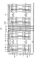
図1に本発明を適用した4バンク構成のシンクロナスDRAMを示す。図中、CHIPは半導体メモリチップ、BANK0〜BANK3はメモリバンク、CKTは全バンクに共通な周辺回路、VDL0〜VDL3およびVDLSは外部電源VDDからメモリアレー用内部電源電圧VDL(第1内部電圧)を発生するための電圧リミッタ回路(又は降圧回路、より一般的には電源回路)、VCL4〜VCL6およびVCLSはVDDから周辺回路用内部電源電圧VCL(第2内部電圧)を発生するための電圧リミッタ回路である。電圧値の一例を示せば、VDD = 3.3 V、 VCL = 2.2 V、VDL = 1.8 Vである。即ち、外部電源電圧VDDから発生された、VDDよりも電圧の低い2種類の内部電圧VCLとVDLが内部回路ブロックに供給されている。VDLはVCLよりも低い電圧とされる。
【0013】
CTL0はVDL0〜VDL3を制御する制御回路、CTL1はVCL4〜VCL6を制御する制御回路である。CTL0とCTL1はCKT内に配置されている。CKT内にはこの他に、ボンディングパッド、入力バッファ、出力バッファ、主制御回路(後述)、メインアンプ、リフレッシュカウンタなどが配置されている。特に制限されないが、入力バッファおよび出力バッファは外部から供給される電源電圧VDDで動作する。
【0014】
各バンクの構成の一例を図2に示す。図中、MAはメモリセルがマトリックス状に配置されたメモリアレー、SCはセンス回路、SWDはサブワード線ドライバ、ISはセンスアンプとサブワード線ドライバとの交点の領域であり、後述のようにセンスアンプ駆動回路が配置されている。
【0015】
第1内部電圧VDLは、センスアンプ駆動回路の電源として用いられる。VDLの配線は寄生抵抗低減のため、メモリアレー上を第2層および第3層メタルを用いてメッシュ状に配置されている。そして、このVDLの配線は図1に示すようにBANK0〜BANK3に渡って配線されている。VDLはまた、VDLの1/2の電圧を発生するVDL/2発生回路(図示せず)にも供給される。電圧VDL/2は後述のように、メモリセルのプレート電極およびビット線プリチャージ用の電源として用いられる。
【0016】
一方、第2内部電圧VCLは、ロウデコーダXD0およびXD1、カラムデコーダYD0およびYD1、バンク専用の周辺回路BCKT、共通周辺回路CKTに供給される。、バンク専用の周辺回路BCKTにはアドレスラッチ、プリデコーダなどが含まれている。ロウデコーダ、カラムデコーダ、および周辺回路BCKT、CKTはVCLを電源として動作するので、VCLの配線がこれらの回路の中を通っている。VCLの配線も図1に示すようにBANK0〜BANK3に渡って配線されている。なお、共通周辺回路CKTに含まれる回路のうち、入力バッファおよび出力バッファは前述のようにVDDで動作するが、その他の大多数の回路は低消費電力化のためVDDよりも低いVCLを電源として動作する。たとえば、主制御回路、メインアンプ、リフレッシュカウンタ、さらには制御回路CTL0およびCTL1もVCLを電源として動作する。
【0017】
図3にメモリアレーMA、センス回路SC、センスアンプ駆動回路ISの詳細を示す。サブワード線SWLとビット線対BL、/BLとの交点にスイッチMOSFETのソース・ドレイン経路の一端に接続されたキャパシタを含むダイナミック形メモリセルMCが周知の折り返し形データ線対方式で配置されている。キャパシタの残る一端であるプレート電極には、VDL/2が共通に供給される。センス回路部には、ビット線対上の信号電圧を増幅するためのセンスアンプSA(交差結合された2つのCOMSインバータ)、ビット線対をVDLの1/2のレベルにプリチャージするためのビット線プリチャージ回路PCなどが配置されている。センスアンプSAを駆動するための1対の信号線NCS、PCSがセンスアンプ駆動回路まで配線されている。信号線NCS、PCSの間にもビット線プリチャージ回路と同様なプリチャージ回路CSPCが設けられVDL/2が供給されている。センスアンプ駆動回路ISは、3個のMOSトランジスタMN1〜MN3から成る。
【0018】
NCSとPCSはいずれも増幅動作をしない時にはCSPCによりVDLの1/2のレベルにプリチャージされている。増幅動作を行うときは、まずMN1とMN2をオンにする。これにより、NCSと接地が、PCSと外部電源VDDがそれぞれ接続されるので、NCSの電位が下降、PCSの電位が上昇する。PCSの電位がVDLレベル近くまで上昇したところで、MN2をオフに、MN3をオンにする。これにより、PCSと内部電源VDLが接続される。最終的にはNCS = 0 V、PCS = VDLとなり、ビット線対の一方が0 V、他方がVDLレベルとなって、増幅動作が完了する。PCSを最初からVDLに接続せずに一旦VDDに接続するのは、増幅動作を高速化するため、およびVDL電圧リミッタ回路の負担を軽減するためである。これはオーバードライブと言われている手法である。
【0019】
図4に各回路間の接続関係を示す。第1内部電圧VDLを発生する電圧リミッタ回路VDL0〜VDL3およびVDLSは、基準電圧発生回路RVG(図1では記載を省略)により発生された基準電圧VRDを参照して、内部電源電圧VDLを発生する。このうち、VDLSは常時動作している、電流供給能力は小さいが消費電流の小さい回路である。VDL0〜VDL3は、消費電流が比較的大きく電流供給能力も大きい回路であり、制御回路CTL0により発生された活性化信号LD0〜LD3によりオン/オフされる。図4でリミッタ回路をあらわす箱の大きさは、各リミッタ回路の電流供給能力の大小を現している。VDL0〜VDL3およびVDLSの出力同士は、図1、図2に示すように、メモリアレー上に第2層(図1、2の実線)および第3層メタル配線(図1、2の点線)を縦横に配置して、接続されている。
【0020】
第2内部電圧VCLを発生する電圧リミッタ回路VCL4〜VCL6およびVCLSは、基準電圧発生回路RVGにより発生された基準電圧VRCを参照して、内部電源電圧VCLを発生する。このうち、VCLSは常時動作している、電流供給能力は小さいが消費電流の小さい回路である。VCL4〜VCL6は、消費電流が比較的大きく電流供給能力も大きい回路である。VCL4は制御回路CTL1により発生された活性化信号LC4によってオン/オフされ、VCL5とVCL6は活性化信号LC5によってオン/オフされる。VCL4〜VCL6およびVCLSの出力同士も接続されている。
【0021】
主制御回路CTLM(図1では記載を省略)は、クロック信号CLK、チップセレクト信号/CS(信号名の前の斜線"/"は補信号であることを示す)、ロウアドレスストローブ/RAS、カラムアドレスストローブ/CAS、書込みエネーブル信号/WE、クロックエネーブル信号CKEなどの信号を受けて、コマンドを解釈し、動作モードを設定する回路である。シンクロナスDRAMでは、クロック信号CLKの立上り時の/CS、/RAS、/CAS、/WE、CKEなどの信号の組み合わせによってコマンドを指定する方法が標準化されており、本実施例もその標準化された方法に従っている。
【0022】
この実施例の特徴は、複数の電圧リミッタの出力同士が接続されていること、および以下に説明するようにメモリの動作モードによって細かく各回路をオン/オフすることである。
【0023】
次に制御回路CTL0について、図5の回路図および図6、図7の動作波形図を参照しながら説明する。入力信号BA0〜BA3はバンクアクティブ信号であり、それぞれメモリバンク0〜3が活性化されているとき"1"、非活性のとき"0"となる。SDRAMで標準化されたバンクアクティブコマンドACTVは、/CS=L、/RAS=L、/CAS=H、/WE=H、ロウアドレス(ワード線を指定するアドレス)、バンクアドレス(バンクの番号を指定するアドレス)により指定される。より一般的なバンクの活性化とは、バンクの場所とそのバンクの中の1ワードを指定し、その1ワード分のデータを対応する複数のセンスアンプに読み出し、ラッチする動作である。RFはリフレッシュ信号であり、メモリがリフレッシュ中のとき"1"になる。出力信号LD0〜LD3は、前述のように、それぞれVDLリミッタ回路VDL0〜VDL3をオン/オフする信号である("1"のときオン、"0"のときオフ)。
【0024】
図6は通常動作の場合の動作波形図である。時刻t0、t1、t2、t3において、それぞれバンク0、バンク1、バンク2、バンク3の活性化コマンド(ACTV 0、ACTV 1、ACTV 2、ACTV 3)が入力され、時刻t4において全バンクプリチャージコマンド(PRE ALL)が入力された場合の波形である。PRE ALLが入力されると、全バンクは非活性となり、各バンクのデータ線対及びセンスアンプ駆動線対はプリチャージ電位VDL/2にプリチャージされる。実際の使用状態においては、バンク活性化とプリチャージとの間に読出しもしくは書込みコマンドが入力されるのが普通であるが、簡単のためここでは省略している。まずBA0が"1"になると、インバータ100-0とワンショットパルス発生回路101-0の働きにより、信号OS0が所定の時間だけ"0"になる。これにより、NANDゲート103-0と104-0とにより構成されたラッチの出力LT0が"1"になり、出力信号LD0が"1"になる。次にBA1が"1"になると、信号OS1が所定の時間だけ"0"になる。これにより、NANDゲート103-1と104-1とにより構成されたラッチの出力LT1が"1"になるとともに、LT0が"0"になる。出力信号LD1は"1"になり、LD0は遅延回路105-0の働きにより所定の時間だけ遅れて"0"になる。次にBA2が"1"になると、同様にして、出力信号LD2が"1"になり、LD1が所定時間だけ遅れて"0"になる。次にBA3が"1"になると、同様にして、出力信号LD3が"1"になり、LD2が所定時間だけ遅れて"0"になる。最後に時刻t4においてBA0〜BA3がすべて"0"になると、ORゲート106の出力IDBが"0"になるので、この時点まで"1"であった信号LT3が"0"になる。出力信号LD3は所定の時間だけ遅れて"0"になる。
【0025】
上の説明から明らかなように、各電圧リミッタ回路VDL0〜VDL3は、自分の近くのメモリバンクの活性化コマンドが入力されたときオンになり、他のバンクの活性化コマンドが入力されたときオフになる。バンク活性化コマンドが入力された直後は、センスアンプが動作するため大電流が流れる。この期間に流れる電流はバンクの近傍にある電圧リミッタ回路から供給される。センスアンプ動作後は電圧レベルを保持するための電流しか流れないので、バンクから遠い回路、あるいは待機時用の電圧リミッタ回路VDLSからでも十分電流を供給できる。前述のように電圧リミッタ回路の出力同士が接続されているからである。このような制御方法をとることにより、複数のメモリバンクが活性化されても、(一時的に2個以上の電圧リミッタ回路がオンになることはあるが)ほとんどの時間帯はオンになっている電圧リミッタ回路はVDLSを除いては1個だけになる。もちろんアクティブスタンバイ状態においても、オンになっている電圧リミッタ回路はVDLSを除いては1個だけである。そのため、動作時はすべての電圧リミッタ回路をオンにする従来方式に比べて、アクティブスタンバイ時の消費電流を著しく低減することができる。シンクロナスDRAMでは、高速データ転送の利点を活かすため、あらかじめバンクを活性化して放置しておくという使われ方が多いので、アクティブスタンバイ電流の低減はシステム全体の消費電流の低減に大きく寄与する。
【0026】
なお、各電圧リミッタ回路を、他バンクの活性化コマンドが入力されたときただちにオフにせずに、所定の時間を置いてからオフにするのは、次のような理由による。前述のようにバンク活性化コマンドが入力された直後は大電流が流れる。大電流が流れる時間は使用するプロセス技術や設計によって異なるが、10〜30ns程度である。一方、バンク活性化コマンドが続けて入力される間隔はシンクロナスDRAMの仕様で定められており、普通は2クロックサイクルである。たとえばクロックの周波数が100MHzならば20nsである。したがって、バンク0の活性化コマンドが入力されて2クロックサイクル後にバンク1の活性化コマンドが入力されたとき、バンク0にまだ大電流が流れている可能性がある。ここでただちに電圧リミッタ回路VDL0をオフすると、その大電流はバンク0から遠い回路VDL1から供給されることになり、配線抵抗による電圧降下によって誤動作あるいは動作遅延が生ずる可能性があり、好ましくない。
【0027】
図7はリフレッシュ時(標準化されたSDRAMのコマンドREFで表されるオートリフレッシュ)の動作波形である。オートリフレッシュコマンドが入力されるとすべてのバンクが同時に活性化され、各バンク毎にリフレッシュカウンタが示すワード線を立ち上げて1ワード分のメモリセルがリフレッシュされる。時刻t5においてリフレッシュコマンド(REF)が入力されると、すべてのバンクアクティブ信号BA0〜BA3、およびリフレッシュ信号RFが"1"になる。これにより、ラッチの出力LT0〜LT3が"1"になり、出力信号LD0〜LD3が"1"になる。チップ内部でリフレッシュ動作が終了すると(このときはコマンドを入力する必要はない)、信号RFおよびBA0〜BA3が"0"になり、ORゲート106の出力IDBが"0"になり、ラッチの出力LT0〜LT3が"0"になり、所定の時間だけ遅れて出力信号LD0〜LD3が"0"になる。すなわち、リフレッシュ時には電圧リミッタ回路VDL0〜VDL3が同時にオンになる。これはリフレッシュ時にはすべてのバンクが同時に動作するので、通常動作時の4倍の電流を供給できるようにするためである。待機時用の電圧リミッタ回路VDLSは常にオンである。
【0028】
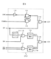
次に制御回路CTL1について、図8の回路図および図9〜図12の動作波形図を参照しながら説明する。入力信号CKEは外部から入力されるクロックエネーブル信号である。PDMBは、後述のパワーダウンモードまたはセルフリフレッシュモードのとき"0"、その他のとき"1"になる信号である。RFはリフレッシュ信号であり、メモリがリフレッシュ中のとき"1"になる。BAはバンクアクティブコマンドが入力されたときに"1"になる信号である。RDおよびWRはそれぞれ、読出しモード、書込みモードにあるときに"1"になる信号である。出力信号LC4は、前述のようにVCLリミッタ回路VCL4をオン/オフする信号である("1"のときオン、"0"のときオフ)。出力信号LC5は、前述のようにVCLリミッタ回路VCL5およびVCL6をオン/オフする信号である("1"のときオン、"0"のときオフ)。
【0029】
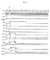
図9はバンク0を活性化しデータを読み出した場合の動作波形図である。時刻t6においてバンク0の活性化コマンド(ACTV 0)が入力されると、信号BAがコマンドが入力されている間だけ"1"になり、遅延回路106の出力DLY1が所定の時間だけ"1"になる。次に、時刻t7においてバンク0の読出しコマンド(READ 0)が入力されると、読出しモードに入るので信号RDが"1"になり、遅延回路108の出力DLY2も"1"になる。時刻t8においてバンク0のプリチャージコマンド(PRE 0)が入力されると、RDが"0"になり、やや遅れてDLY2も"0"になる。出力信号LC5はDLY1とDLY2とのORであるから、バンク活性化コマンド入力直後と読出しモードのときに"1"になる。出力信号LC4は、クロックエネーブル信号CKEが"1"であるから、常に"1"である。
【0030】
したがって、バンク活性化コマンド入力直後と読出しモードのときは電圧リミッタ回路VCL4〜VCL6およびVCLSがすべてオンになり、その他のときはVCL4とVCLSのみがオンでVCL5とVCL6はオフになる。バンク活性化コマンド入力直後は、アドレスバッファやロウデコーダなどが動作するため、大電流が流れる。また読出しモードのときも、カラムデコーダ、メインアンプ、出力バッファなどが動作するために大電流が流れる。そこで、これらの期間にはすべての電圧リミッタ回路をオンにして大電流を供給できるようにしている。その他の期間に流れる電流は小さいため、一部の回路をオフにしている。即ちVCL5やVCL6の動作期間は、バンク活性化や読み出しに伴って動作するロウデコーダやカラムデコーダ等の動作期間とほぼ同じか余裕を見て少し長くなるように設定する。このような制御方法をとることにより、アクティブスタンバイ状態(バンク活性化から読出しコマンドまでの間)にはオンになっている電圧リミッタ回路はVCLSを除いては1個だけになる。そのため、動作時はすべての電圧リミッタ回路をオンにする従来方式に比べて、アクティブスタンバイ時の消費電流を著しく低減することができる。
【0031】
上に述べたのは読出しの場合であるが、書込みの場合も信号RDのかわりにWRが"1"になることを除いては、動作は同じであり、同様にアクティブスタンバイ電流を低減することができる。
【0032】
図10はリフレッシュ時(オートリフレッシュ)の動作波形である。図7の場合と同様に、時刻t5においてリフレッシュコマンド(REF)が入力されると、リフレッシュ動作が行われている間だけリフレッシュ信号RFが"1"になる。出力信号LC5は、ワンショットパルス発生回路114と遅延回路116の働きによって、RFの立上りから所定の時間だけ"1"になり、その後は"0"になる。クロックエネーブル信号CKEが"1"であるから、出力信号LC4は常に"1"である。したがって、リフレッシュ動作開始直後は電圧リミッタ回路VCL4〜VCL6とVCLSがすべてオンになり、その後はVCL5とVCL6はオフになる。リフレッシュ動作開始直後はロウデコーダなどが動作するため、大電流が流れる。そこで、この期間にはすべての電圧リミッタ回路をオンにして大電流を供給できるようにしている。その後はほとんど電流が流れないため、一部の回路をオフにし、消費電流の低減を図っている。
【0033】
図11はパワーダウンモード時の動作波形である。パワーダウンモードとは、通常のDRAMにおける待機状態(全てのデータ線をVDL/2にプリチャージしている状態)に相当する低消費電力モードのことである。クロックエネーブル信号CKEなどによってパワーダウンモード開始/終了を指定する方法が標準化されており、本実施例もその標準化された方法に従っている。時刻t9においてパワーダウンモード開始コマンド(PDM Entry)が入力されると、信号PDMBが"0"になるので、出力信号LC4が"0"になる。時刻t10においてパワーダウンモード終了コマンド(PDM Exit)が入力されるが、信号CKEがそれに先立って"1"になっているので、この時点でLC4が"1"になる。パワーダウンモードの間はLC4もLC5も"0"になるから、電圧リミッタ回路VCL4〜VCL6はすべてオフになり、待機時用電圧リミッタ回路VCLSのみがオンである。したがって、パワーダウンモードの間の消費電流はきわめて少なくなる。
【0034】
なお、信号LC4の立下りはPDMBによって決めているが、立上りはCKEによって決めている理由は次のとおりである。シンクロナスDRAMの規格によれば、パワーダウンモード終了はクロック信号CLKの立上りエッジでのCKEを"1"にすることによって指定する。CKEを"1"にするのはCLKの立上りよりもセットアップ時間(普通は2〜3ns)だけ前でなければならない。したがって、パワーダウンモード終了をCKEによって判断する方がPDMBによって判断するよりも、LC4の立上りを早くできる。パワーダウンモード終了コマンドの次のクロックサイクルにはバンクアクティブなどのコマンドが入力される可能性があるので、これに備えて電圧リミッタVCL4を早めにオンにしておくのが望ましい。
【0035】
図12はセルフリフレッシュモード時の動作波形である。セルフリフレッシュコマンドが入力されるとセルフリフレッシュ終了コマンドが入力されるまで、SDRAMは内部タイマーにより周期的にリフレッシュを実行する。時刻t11においてセルフリフレッシュモード開始コマンド(SELF Entry)が入力されると、信号PDMBが"0"になるので、出力信号LC4が"0"になる。チップ上に設けられたタイマーによって時刻t12にリフレッシュ動作が開始されると、信号RFが"1"になる。出力信号LC4はRFが"1"になっている間"1"になる。出力信号LC5はRFの立上りから所定の時間だけ"1"になる。時刻t13においてセルフリフレッシュモード終了コマンド(SELF Exit)が入力されるが、信号CKEがそれに先立って"1"になっているので、この時点でLC4が"1"になる。したがってセルフリフレッシュモードのときは、電圧リミッタ回路VCL4〜VCL6は、実際にリフレッシュ動作が行われているときにはオンになるが、その他の時間帯はオフである。リフレッシュ動作が行われる間隔は普通数十〜数百μsであり、1回のリフレッシュ動作は数十nsで完了するから、リフレッシュ動作が行われている時間は全体の時間の0.1%以下である。その他の大部分の時間帯には、電圧リミッタ回路VCL4〜VCL6はすべてオフになり、待機時用電圧リミッタ回路VCLSのみがオンであるから、セルフリフレッシュモードの消費電流はきわめて少なくなる。
【0036】
図13はVCL電圧リミッタ回路の一例である。この回路は差動増幅器DAと出力段FSから成る。差動増幅器DAは、活性化信号LCiが"1"(高レベル)のとき活性化され、出力電圧VCLを2個のPチャネルMOSトランジスタM19、M20で分圧した電圧VFBと基準電圧VRCとを比較する。その出力PGは出力段のPチャネルMOSトランジスタM16のゲートに入力されている。VCLの電位が低下したときはPGの電位が下がり、M16がオンしてVDDからVCLに電荷が供給される。VCLの電位が上がり過ぎたときは、NチャネルMOSトランジスタM17、M18から成るリーク回路を通して電荷が放電される。活性化信号LCiが"0"(低レベル)のときは、NチャネルMOSトランジスタM1がオフ、PチャネルMOSトランジスタM8、M9、M15がオン、NチャネルMOSトランジスタM14がオンになる。これにより、PチャネルMOSトランジスタM4〜M7およびNチャネルMOSトランジスタM12、M13がオフになるので、差動増幅器DAに流れていた電流はすべてカットオフされる。さらに、出力段のM16およびM18もオフになる。したがって、消費電流は分圧回路M19、M20に流れる電流のみとなり、動作状態に比べてきわめて少なくなる。M19、M20に常時電流を流しておくには、次に差動増幅器DAが動作開始するときに備えて、電圧VFBのレベルを安定に保持しておくためである。
【0037】
図14はVDL電圧リミッタの一例である。図13の回路との相違点は、出力電圧VDLの電位が上昇し過ぎたときに電荷を放電する機能が強化されていることである。差動増幅器DAは2つの出力PG、NGを有する。PGは図13の回路と同様に、PチャネルMOSトランジスタM16に入力されており、一方NGはNチャネルMOSトランジスタM25のゲートに入力されている。VDLの電位が上昇し過ぎたときは、NGの電位が上がり、M25を通してVDLの電荷が放電される。オーバードライブ方式(図3参照)を用いている場合はVDLの電位が上昇し過ぎる可能性があるので、これに対処するためである。 本実施例は、4個のバンクを例にして説明したが、バンクの数は整数であれば良いが、2、4、8、16、32のような2のべき乗であれば更に好ましい。残る実施例も4バンク構成を例に取るが、バンク数は同様に4個には制限されない。
【0038】
第1内部電圧VDLを発生する電圧リミッタ回路(待機時用を除く)の数は、バンク数(本実施例では4)に等しくすることにより、上述のような制御が可能になる。一方、第2内部電圧VCLを発生する電圧リミッタ回路(待機時用を除く)は、本実施例では3個であるが、2個以上であればよい。すなわち、制御信号LC4とLC5で制御される回路がそれぞれ1個以上あればよい。待機時用の電圧リミッタ回路は、VDL用とVCL用が各1個以上あればよいが、待機時消費電流低減のためには各1個とするのが望ましい。
【0039】
〔実施例2〕
次に、本発明の第2の実施例について説明する。回路の配置は図1と同じであるからここでは省略し、図15に回路間の接続関係を示す。図4との相違点は、電圧リミッタ回路VDL0とVDL1とをまとめて、活性化信号LD0で制御していることである。VDL2とVDL3についても同様に、活性化信号LD2で制御している。
【0040】
制御回路CTL0の回路図を図16に、動作波形を図17に示す。図6の場合と同様に、時刻t0、t1、t2、t3において、それぞれバンク0、バンク1、バンク2、バンク3の活性化コマンドが入力され、時刻t4において全バンクプリチャージコマンドが入力された場合の波形である。まずBA0が"1"になると、図6の場合と同様に、信号OS0が所定の時間だけ"0"になり、NANDゲート103-0と104-0とにより構成されたラッチの出力LT0が"1"になり、出力信号LD0が"1"になる。次にBA1が"1"になると、信号OS1が所定の時間だけ"0"になるが、このときはラッチの出力LT0、LT2は変化しない。次にBA2が"1"になると、信号OS2が所定の時間だけ"0"になる。これにより、NANDゲート103-2と104-2とにより構成されたラッチの出力LT2が"1"になるとともに、LT0が"0"になる。出力信号LD2は"1"になり、LD0は遅延回路105-0の働きにより所定の時間だけ遅れて"0"になる。次にBA3が"1"になると、信号OS3が所定の時間だけ"0"になるが、このときはラッチの出力LT0、LT2は変化しない。最後に時刻t4においてBA0〜BA3がすべて"0"になると、ORゲート106の出力IDBが"0"になるので、この時点まで"1"であった信号LT2が"0"になる。出力信号LD2は所定の時間だけ遅れて"0"になる。
【0041】
なお、電圧リミッタ回路VDL0とVDL1とは、常に同時にオン/オフされるので、まとめて1つの回路としてもよい。VDL2とVDL3についても同様である。
【0042】
本実施例では、2個の電圧リミッタをまとめて1つの活性化信号で制御しているため、ほとんどの時間帯にはVDLS以外に2個の電圧リミッタ回路がオンになっている。したがって、消費電流低減効果は実施例1に比べて劣るが、制御回路が簡単になり、活性化信号の数も少なくなるという利点がある。これは特にバンク数が多い場合に有効である。たとえば、16個のバンクを有するメモリの場合、各バンクに1個の電圧リミッタ回路を個別に制御すれば16本の活性化信号が必要であるが、4個ずつまとめて制御すれば4本の活性化信号ですむ。
【0043】
制御回路CTL1は実施例1(図8)と同じであるから、説明は省略する。
【0044】
本実施例では、VDL用電圧リミッタ回路(待機時用を除く)の数はバンク数と同じく4個としているが、VDL0とVDL1は同じ制御信号LD0によって制御され、同時にオン/オフされるので、まとめて1つの回路としてもよい。VDL2とVDL3についても同様である。このように同じ制御信号で制御される回路を1つにまとめると、VDL用電圧リミッタ回路の数はバンク数の約数となる。
【0045】
〔実施例3〕
図18に本発明の第3の実施例を示す。図1との相違点はVDL用の電圧リミッタ回路VDL4が追加されていることである。この回路は、図19に示すように活性化信号LC4によって制御される。
【0046】
制御回路CTL0の回路図を図20に、動作波形を図21に示す。図6、図17の場合と同様に、時刻t0、t1、t2、t3において、それぞれバンク0、バンク1、バンク2、バンク3の活性化コマンドが入力され、時刻t4において全バンクプリチャージコマンドが入力された場合の波形である。まずBA0が"1"になると、ワンショットパルス発生回路108-0の出力OS10が所定の時間だけ"1"になる。これにより、出力信号LD0が"1"になり、遅延回路105-0の働きにより所定の時間だけ遅れて"0"になる。BA1、BA2、BA3が"1"になったときも同様に、それぞれLD1、LD2、LD3が所定の時間だけ"1"になる。一方、LC4はここでは常に"1"である。
【0047】
したがって、各電圧リミッタ回路VDL0〜VDL3は、自分の近くのメモリバンクの活性化コマンドが入力された直後のみオンになり、VDL4は常にオンである。バンク活性化コマンドが入力された直後は、センスアンプが動作するため大電流が流れる。この期間に流れる電流は主としてバンクの近傍にある電圧リミッタ回路から供給される。センスアンプ動作後に流れる電流は小さいので、VDL4あるいはVDLSからでも十分供給できる。このような制御方法をとることにより、複数のメモリバンクが活性化されても、(一時的に2個以上の電圧リミッタ回路がオンになることはあるが)ほとんどの時間帯はオンになっている電圧リミッタ回路はVDLSとVDL4だけである。もちろんアクティブスタンバイ状態においても、オンになっている電圧リミッタ回路はVDLSとVDL4だけである。そのため、動作時はすべての電圧リミッタ回路をオンにする従来方式に比べて、アクティブスタンバイ時の消費電流を著しく低減することができる。
【0048】
以上の説明から明らかなように、電圧リミッタ回路VDL4の電流供給能力はVDL0〜VDL3に比べて小さくてもよい。しかし、VDLSよりは大きいことが望ましい。なぜならば、書き込みモードのときには、ビット線対の電位を反転するための電流が流れ、この電流は(VDL0〜VDL3がオフになっているので)VDL4から供給されるからである。なお、VDL4は活性化信号LC4によって制御されているので、パワーダウンモードやセルフリフレッシュのときにはオフになる(図11、12参照)。
【0049】
本実施例の利点は、制御回路CTL0が簡単になることである。これは図20と図5、図16を比較してみれば明らかである。
【0050】
制御回路CTL1は実施例1(図8)と同じであるから、説明は省略する。
【0051】
本実施例の場合は、バンクの数を変えた時、VDL用電圧リミッタ回路(待機時用を除く)の数はバンク数+1以上であればよい。すなわち、各バンクに対応した回路が1個ずつと、LC4によって制御される回路が1個以上である。
【0052】
〔実施例4〕
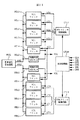
図22に本発明の第4の実施例を示す。本実施例の特徴は、VCL用の電圧リミッタ回路にVDL用と同様の制御方式(実施例3)を適用したことである。VCL用の電圧リミッタ回路は、各バンクの近傍に1個ずつ(VCL0〜VCL3)配置され、中央にVCL4と待機時用のVCLSが配置されている。図4に各回路間の接続関係を示す。VDL用電圧リミッタ回路VDL0〜VDL4はそれぞれ、実施例3(図19)と同様に、活性化信号LD0、LD1、LD2、LD3、LC4によって制御される。VCL用電圧リミッタ回路VCL0〜VCL4はそれぞれ、活性化信号LC0、LC1、LC2、LC3、LC4によって制御される。
【0053】
制御回路CTL0は実施例3(図20)と同じであるから説明は省略し、制御回路CTL1について図24の回路図と図25の動作波形図を用いて説明する。図9の場合と同様に、バンク0を活性化しデータを読み出した場合である。まず時刻t6においてバンク0活性化コマンドが入力され、信号BA0が"1"になると、ワンショットパルス発生回路120-0の出力OS20が所定の時間だけ"1"になる。これにより、出力信号LC0が"1"になり、遅延回路122-0の働きにより所定の時間だけ遅れて"0"になる。次に、時刻t7においてバンク0の読出しコマンドが入力されると、読出しモードに入るので信号RDが"1"になり、出力信号LC0〜LC3がすべて"1"になる。時刻t8においてバンク0のプリチャージコマンド(PRE 0)が入力されると、RDが"0"になり、やや遅れてLC0〜LC3も"0"になる。出力信号LC4は、クロックエネーブル信号CKEが"1"であるから、常に"1"である。
【0054】
したがって、バンク活性化コマンド入力直後は電圧リミッタ回路VCL0、VCL4、VCLSがオンになり、読出しモードのときはVCL0〜VCL4およびVCLSがすべてオンになり、その他のときはVCL4とVCLSのみがオンになる。バンク活性化コマンド入力直後と読出しモードのときは大電流が流れるので、これらの期間にはオンにする電圧リミッタ回路の数を多くして大電流を供給できるようにしている。その他の期間に流れる電流は小さいため、オンにする電圧リミッタ回路の数を少なくしている。このような制御方法をとることにより、アクティブスタンバイ状態(バンク活性化から読出しコマンドまでの間)にはオンになっている電圧リミッタ回路はVCL4とVCLSだけになる。そのため、動作時はすべての電圧リミッタ回路をオンにする従来方式に比べて、アクティブスタンバイ時の消費電流を著しく低減することができる。
【0055】
以上の説明から明らかなように、電圧リミッタ回路VCL4の電流供給能力はVCL0〜VCL3に比べて小さくてもよい。しかし、VCLSよりは大きいことが望ましい。なぜならば、アクティブスタンバイ状態でもごく一部の回路(クロック信号CLKの入力バッファなど)は動作しているからである。なお、VCL4は活性化信号LC4によって制御されているので、パワーダウンモードやセルフリフレッシュのときにはオフになる(図11、12参照)。
【0056】
上に述べたのは読出しの場合であるが、書込みの場合も信号RDのかわりにWRが"1"になることを除いては、動作は同じであり、同様にアクティブスタンバイ電流を低減することができる。
【0057】
本実施例の場合は、VDL用、VCL用とも電圧リミッタ回路(待機時用を除く)の数はバンク数+1以上であればよい。すなわち、各バンクに対応した回路が1個ずつと、LC4によって制御される回路が1個以上である。
【0058】
〔実施例5〕
図26に本発明の第5の実施例を示す。実施例1との相違点は、入力バッファ用に専用の内部電源電圧VIIを発生していること、およびメモリアレー用内部電源電圧VDLと周辺回路用内部電源電圧VCLのレベルが等しいことである。電圧値の一例を示せば、VDD = 3.3 V、VCL = VDL = 1.8 V、VII = 2.5 Vである。入力バッファは入力信号の高レベルVIH、低レベルVILなどの規格を満足するため、電源電圧が安定であることが望ましい。そこで、専用電源を電圧リミッタ回路VII0〜VII2およびVIISによって発生している。前述のように入力バッファは周辺回路CKT内に配置されているので、VIIの配線がCKT内を通っている。
【0059】
図27に各回路間の接続関係を示す。大要は実施例1(図4)と同じであるから、相違点についてのみ説明する。内部電源電圧VIIを発生するために、電圧リミッタ回路VII0〜VII2およびVIISが追加されている。これらの回路は、基準電圧発生回路RVG(図26では記載を省略)により発生された基準電圧VRIを参照して、内部電源電圧VIIを発生する。このうち、VIISは常時動作している、電流供給能力は小さいが消費電流の小さい回路である。VII0〜VII2は、消費電流が比較的大きく電流供給能力も大きい回路であり、活性化信号LC4によってオン/オフされる。したがって、VII0〜VII2はパワーダウンモードやセルフリフレッシュのとき以外は常にオンである。
【0060】
内部電源電圧VDLとVCLのレベルが等しいため、VDL電圧リミッタ回路とVCL電圧リミッタ回路は、共通の基準電圧VRCを利用している。また、待機時用VDL電圧リミッタ回路VDLSが省略されている。そのかわりに、VDLとVCLとが適当な抵抗(図27ではMOSトランジスタMCで代用)で接続されている。全バンクが非活性状態の時は電圧リミッタ回路VDL0〜VDL3はオフであるから、このときのVDLのレベルはMCを通してVCL電圧リミッタ回路によって保持される。このように、VDLとVCLのレベルが等しいときは、VDLSを省略することにより、パワーダウンモードやセルフリフレッシュのときの消費電流をその分だけ低減することができる。
【0061】
本実施例では、VDL用とVCL用の電圧リミッタ回路(待機時用を除く)の数は、実施例1と同様に選ぶことができる。また、VII用電圧リミッタ回路(待機時用は除く)は本実施例では3個設けているが、1個以上であればよい。本実施例の場合、上述のように待機時用VDL電圧リミッタ回路を省略できるのが特徴である。
【0062】
以上、本発明をシンクロナスDRAMに適用した実施例を示した。しかし本発明は、複数のバンクを有し、コマンドに動作が指定され半導体メモリ(例えば、DDR(ダブル・データ・レート)-SDRAM、Synclink-DRAM、Rambus-DRAM)ならば、具体的なコマンドの形式は異なっても適用可能である。1つのチップに同様なDRAMと論理回路、CPUなどを混載した半導体装置にも適用可能である。SDRAMのアクティブスタンバイ状態と同様にセンスアンプにデータを読み出しラッチして保持するメモリを有する半導体装置に適用するのが特に効果的である。
【0063】
【発明の効果】
以上説明したように、本発明によれば、アクティブスタンバイ状態にあるときのオンチップ電圧リミッタ回路の消費電流を低減できる。
【図面の簡単な説明】
【図1】本発明の第1の実施例であるシンクロナスDRAMを示す図である。
【図2】図1のシンクロナスDRAMの1つのバンクの構成図である。
【図3】図2のバンクの一部の詳細回路図である。
【図4】図1のシンクロナスDRAMの電源回路の構成図である。
【図5】図1のシンクロナスDRAMの電圧リミッタ制御回路CTL0の回路図である。
【図6】図5の制御回路の動作波形図である。
【図7】図5の制御回路の動作波形図である。
【図8】図1のシンクロナスDRAMの電圧リミッタ制御回路CTL1の回路図である。
【図9】図8の制御回路の動作波形図である。
【図10】図8の制御回路の動作波形図である。
【図11】図8の制御回路の動作波形図である。
【図12】図8の制御回路の動作波形図である。
【図13】図1のシンクロナスDRAMの電圧リミッタ回路VDL0〜VDL3の回路図である。
【図14】図1のシンクロナスDRAMの電圧リミッタ回路VCL4〜VCL6の回路図である。
【図15】本発明の第2の実施例であるシンクロナスDRAMの電源回路の構成図である。
【図16】図15のシンクロナスDRAMの電圧リミッタ制御回路CTL0の回路図である。
【図17】図16の制御回路の動作波形図である。
【図18】本発明の第3の実施例であるシンクロナスDRAMを示す図である。
【図19】図18のシンクロナスDRAMの電源回路の構成図である。
【図20】図18のシンクロナスDRAMの電圧リミッタ制御回路CTL0の回路図である。
【図21】図20の制御回路の動作波形図である。
【図22】本発明の第4の実施例であるシンクロナスDRAMを示す図である。
【図23】図22のシンクロナスDRAMの電源回路の構成図である。
【図24】図22のシンクロナスDRAMの電圧リミッタ制御回路CTL1の回路図である。
【図25】図24の制御回路の動作波形図である。
【図26】本発明の第5の実施例であるシンクロナスDRAMを示す図である。
【図27】図26のシンクロナスDRAMの電源回路の構成図である。
【符号の説明】
CHIP……チップ、BANK0、BANK1、BANK2、BANK3……メモリバンク、CKT……周辺回路、VDL0〜VDL4……動作時用VDL電圧リミッタ回路、VDLS……待機時用VDL電圧リミッタ回路、VCL0〜VCL6……動作時用VDD電圧リミッタ回路、VCLS……待機時用VDD電圧リミッタ回路、CTL0……VDL電圧リミッタ制御回路、CTL1……VDD電圧リミッタ制御回路、CTLM……主制御回路、RVG……基準電圧発生回路。[0001]
BACKGROUND OF THE INVENTION
The present invention relates to a power supply circuit for a semiconductor memory, and more particularly to a control method suitable for low power consumption.
[0002]
[Prior art]
References referred to in this specification are as follows. [Document 1]: JP-A-7-105682. [Document 2]: JP-A-9-161481.
[0003]
A so-called on-chip voltage limiter method (step-down method) that generates an internal voltage obtained by stepping down an external power supply voltage on a semiconductor chip and uses this as a power source is widely used in semiconductor memories and the like. This is to reduce the current consumption of the circuit or to ensure the reliability of the fine elements. A circuit that generates an internal power supply voltage for this purpose is a voltage limiter circuit (step-down circuit).
[0004]
The voltage limiter circuit consumes a steady current to maintain the output voltage level even when the semiconductor memory is in a standby state. As one of the methods for reducing the current consumption during standby, [Document 1] is provided in common with a total of eight voltage limiter circuits, two for each of four memory cell arrays. One common voltage limiter circuit is described (FIG. 3 of [Document 1]). The common voltage limiter circuit always operates, and the eight voltage limiter circuits are controlled so that when the memory is accessed, the eight start the operation all at once, and the four operate after a predetermined period.
[0005]
[Document 2] describes the first and second voltage limiters provided corresponding to the first and second banks and their operation timing. When the activation of the first bank is instructed, the first voltage limiter generates an internal voltage. When the activation of the second bank is instructed while the first bank is still activated, the second voltage limiter is also the first voltage limiter. It is described that an internal voltage is generated together with a voltage limiter (FIG. 12 of [Document 2]).
[0006]
[Problems to be solved by the invention]
Prior to the present application, the inventors of the present application examined the current consumption in the active standby state of the SDRAM (Synchronous Dynamic Random Access Memory). The active standby state in the SDRAM is a state in which a memory bank is activated to hold data for one specific word in the sense amplifier in preparation for memory access and is left without applying a read / write command. Reading data from a dynamic memory cell takes a relatively long time, but once it is held in a sense amplifier, the data held in that sense amplifier is as if it were an SRAM (static random access memory). ) So that it can be read out at high speed.
[0007]
After applying the bank activation command to set the active standby state, the word line is selected and the sense amplifier operates, so that a large current flows, but in principle, no current consumption should flow when left unattended. It is. However, if there is a voltage limiter circuit, the current consumption flows. At this time, if both the standby circuit and the operation circuit are operating, the current consumption of the voltage limiter is considerably large (usually several mA to several tens of mA). In particular, in the case of a synchronous DRAM, in order to take advantage of the high-speed data transfer, the bank is often activated and left in advance. Therefore, the active standby current greatly affects the current consumption of the entire system.
[0008]
In the configuration of [Reference 1] described above, since the operation depending on the bank peculiar to the SDRAM is not considered, as many as eight voltage limiter circuits operate simultaneously, and the peak operating current becomes too large. Not considered. Even in the active standby state, as many as four voltage limiter circuits operate (including the common voltage limiter circuit), the active standby current becomes unnecessarily large.
[0009]
In [Document 2], the active standby state is not taken into consideration, and when a plurality of memory banks are activated one after another, the corresponding voltage limiter circuit additionally operates, and the plurality of memory banks are set to active standby. It does not take into consideration that the operating current of the limiter circuit is unnecessarily added in this state. This becomes a serious problem especially when the number of banks is large.
[0010]
[Means for Solving the Problems]
A typical configuration for solving the above problems is as follows. That is, the first and second memory banks activated by the first and second commands, respectively, are wired across the first and second memory banks, and a predetermined voltage is supplied to the first and second memory banks. And first and second power supply circuits provided corresponding to each of the first and second memory banks, each output node being coupled to the power supply wiring, and generating the predetermined voltage. In response to the first command, the first power supply circuit starts generating the predetermined voltage, and when the second command is input while maintaining the active state of the first memory bank, The first power supply circuit stops generating the predetermined voltage in response to the second command, and the second power supply circuit starts generating the predetermined voltage in response to the second command.
[0011]
DETAILED DESCRIPTION OF THE INVENTION
Embodiments of the present invention will be described below in detail with reference to the drawings. The circuit elements constituting each block of the embodiment are not particularly limited, but are formed on a single semiconductor substrate such as single crystal silicon by a known integrated circuit technology such as CMOS (complementary MOS transistor). A MOSFET circuit symbol without an arrow represents an N-type MOSFET (NMOS) and is distinguished from a P-type MOSFET (PMOS) with an arrow.
[0012]
[Example 1]
FIG. 1 shows a 4-bank synchronous DRAM to which the present invention is applied. In the figure, CHIP is a semiconductor memory chip, BANK0 to BANK3 are memory banks, CKT is a peripheral circuit common to all banks, VDL0 to VDL3 and VDLS are internal power supply voltage VDL (first internal voltage) for memory array from external power supply VDD Voltage limiter circuit for generating voltage (or step-down circuit, more generally power supply circuit), VCL4 to VCL6 and VCLS are voltage limiter circuits for generating internal power supply voltage VCL (second internal voltage) for peripheral circuits from VDD It is. An example of voltage values is VDD = 3.3 V, VCL = 2.2 V, and VDL = 1.8 V. That is, two types of internal voltages VCL and VDL generated from the external power supply voltage VDD and having a voltage lower than VDD are supplied to the internal circuit block. VDL is a voltage lower than VCL.
[0013]
CTL0 is a control circuit that controls VDL0 to VDL3, and CTL1 is a control circuit that controls VCL4 to VCL6. CTL0 and CTL1 are arranged in CKT. In addition to this, a bonding pad, an input buffer, an output buffer, a main control circuit (described later), a main amplifier, a refresh counter, and the like are arranged in the CKT. Although not particularly limited, the input buffer and the output buffer operate with the power supply voltage VDD supplied from the outside.
[0014]
An example of the configuration of each bank is shown in FIG. In the figure, MA is a memory array in which memory cells are arranged in a matrix, SC is a sense circuit, SWD is a sub-word line driver, IS is an area at the intersection of the sense amplifier and the sub-word line driver. A drive circuit is arranged.
[0015]
The first internal voltage VDL is used as a power source for the sense amplifier driving circuit. The VDL wiring is arranged in a mesh shape on the memory array using the second layer and the third layer metal to reduce parasitic resistance. The VDL wiring is routed across BANK0 to BANK3 as shown in FIG. VDL is also supplied to a VDL / 2 generation circuit (not shown) that generates a voltage half that of VDL. As will be described later, voltage VDL / 2 is used as a power supply for the plate electrode and bit line precharge of the memory cell.
[0016]
On the other hand, the second internal voltage VCL is supplied to the row decoders XD0 and XD1, the column decoders YD0 and YD1, the bank-specific peripheral circuit BCKT, and the common peripheral circuit CKT. The bank-specific peripheral circuit BCKT includes an address latch, a predecoder, and the like. Since the row decoder, the column decoder, and the peripheral circuits BCKT and CKT operate using VCL as a power source, the wiring of the VCL passes through these circuits. VCL wiring is also routed across BANK0 to BANK3 as shown in FIG. Of the circuits included in the common peripheral circuit CKT, the input buffer and the output buffer operate at VDD as described above. However, most other circuits use VCL lower than VDD as the power source to reduce power consumption. Operate. For example, the main control circuit, the main amplifier, the refresh counter, and the control circuits CTL0 and CTL1 also operate using VCL as a power source.
[0017]
FIG. 3 shows details of the memory array MA, the sense circuit SC, and the sense amplifier drive circuit IS. A dynamic memory cell MC including a capacitor connected to one end of the source / drain path of the switch MOSFET is arranged at the intersection of the sub word line SWL and the bit line pair BL, / BL by a well-known folded data line pair system. . VDL / 2 is commonly supplied to the plate electrode which is the other end of the capacitor. The sense circuit section includes a sense amplifier SA (two cross-coupled COMS inverters) for amplifying the signal voltage on the bit line pair, and a bit for precharging the bit line pair to a level half of VDL. A line precharge circuit PC and the like are arranged. A pair of signal lines NCS and PCS for driving the sense amplifier SA are wired to the sense amplifier drive circuit. A precharge circuit CSPC similar to the bit line precharge circuit is also provided between the signal lines NCS and PCS, and VDL / 2 is supplied. The sense amplifier drive circuit IS is composed of three MOS transistors MN1 to MN3.
[0018]
Both NCS and PCS are precharged to half the level of VDL by CSPC when not performing an amplification operation. When performing an amplification operation, first, MN1 and MN2 are turned on. As a result, the NCS and the ground are connected, and the PCS and the external power supply VDD are connected to each other, so that the potential of the NCS decreases and the potential of the PCS increases. When the PCS potential rises to near the VDL level, MN2 is turned off and MN3 is turned on. As a result, the PCS and the internal power supply VDL are connected. Eventually, NCS = 0 V and PCS = VDL, one of the bit line pairs becomes 0 V, and the other becomes the VDL level, and the amplification operation is completed. The reason why PCS is once connected to VDD without being connected to VDL from the beginning is to speed up the amplification operation and to reduce the burden on the VDL voltage limiter circuit. This is a technique called overdrive.
[0019]
Fig. 4 shows the connection between the circuits. Voltage limiter circuits VDL0 to VDL3 and VDLS that generate first internal voltage VDL generate internal power supply voltage VDL by referring to reference voltage VRD generated by reference voltage generation circuit RVG (not shown in FIG. 1). . Among these, VDLS is a circuit that is always operating and has a small current supply capability but a small current consumption. VDL0 to VDL3 are circuits having a relatively large current consumption and a large current supply capability, and are turned on / off by activation signals LD0 to LD3 generated by the control circuit CTL0. The size of the box representing the limiter circuit in FIG. 4 represents the magnitude of the current supply capability of each limiter circuit. As shown in FIGS. 1 and 2, the outputs of VDL0 to VDL3 and VDLS are connected to the second layer (solid lines in FIGS. 1 and 2) and the third layer metal wiring (dotted lines in FIGS. 1 and 2) on the memory array. They are connected vertically and horizontally.
[0020]
Voltage limiter circuits VCL4 to VCL6 and VCLS for generating second internal voltage VCL generate internal power supply voltage VCL with reference to reference voltage VRC generated by reference voltage generation circuit RVG. Among them, the VCLS is always operating, and is a circuit that has a small current supply capability but a small current consumption. VCL4 to VCL6 are circuits with relatively large current consumption and large current supply capability. VCL4 is turned on / off by an activation signal LC4 generated by the control circuit CTL1, and VCL5 and VCL6 are turned on / off by an activation signal LC5. The outputs of VCL4 to VCL6 and VCLS are also connected.
[0021]
The main control circuit CTLM (not shown in FIG. 1) includes a clock signal CLK, a chip select signal / CS (the hatched “/” in front of the signal name indicates a complementary signal), a row address strobe / RAS, a column This circuit receives signals such as the address strobe / CAS, write enable signal / WE, and clock enable signal CKE, interprets the command, and sets the operation mode. In synchronous DRAM, the method of specifying commands by combining signals such as / CS, / RAS, / CAS, / WE, and CKE at the rising edge of the clock signal CLK has been standardized, and this example has also been standardized. Follow the method.
[0022]
The feature of this embodiment is that the outputs of a plurality of voltage limiters are connected to each other, and that each circuit is finely turned on / off depending on the operation mode of the memory as described below.
[0023]
Next, the control circuit CTL0 will be described with reference to the circuit diagram of FIG. 5 and the operation waveform diagrams of FIGS. The input signals BA0 to BA3 are bank active signals, which are “1” when the
[0024]
FIG. 6 is an operation waveform diagram in the normal operation. At time t0, t1, t2, t3, activation commands (
[0025]
As apparent from the above description, each of the voltage limiter circuits VDL0 to VDL3 is turned on when an activation command of a memory bank near itself is inputted, and is turned off when an activation command of another bank is inputted. become. Immediately after the bank activation command is input, a large current flows because the sense amplifier operates. The current flowing during this period is supplied from a voltage limiter circuit in the vicinity of the bank. Since only a current for holding the voltage level flows after the sense amplifier operation, a sufficient current can be supplied from a circuit far from the bank or the voltage limiter circuit VDLS for standby. This is because the outputs of the voltage limiter circuit are connected as described above. By adopting such a control method, even when a plurality of memory banks are activated, two or more voltage limiter circuits may be temporarily turned on (although it may be temporarily turned on), most of the time zones are turned on. There is only one voltage limiter circuit except for VDLS. Of course, even in the active standby state, only one voltage limiter circuit is turned on except for VDLS. Therefore, the current consumption during active standby can be significantly reduced as compared with the conventional method in which all voltage limiter circuits are turned on during operation. In synchronous DRAM, in order to take advantage of high-speed data transfer, the bank is often activated and left in advance, so the reduction of the active standby current greatly contributes to the reduction of the current consumption of the entire system.
[0026]
It is to be noted that each voltage limiter circuit is not turned off immediately after an activation command of another bank is input, but is turned off after a predetermined time, for the following reason. As described above, a large current flows immediately after the bank activation command is input. The time during which a large current flows is about 10 to 30 ns, although it depends on the process technology and design used. On the other hand, the interval at which the bank activation command is continuously input is determined by the specification of the synchronous DRAM, and is usually two clock cycles. For example, if the clock frequency is 100 MHz, it is 20 ns. Therefore, when the
[0027]
FIG. 7 shows operation waveforms at the time of refresh (auto refresh represented by a standard SDRAM command REF). When an auto-refresh command is input, all banks are activated at the same time, and the word line indicated by the refresh counter is raised for each bank to refresh memory cells for one word. When a refresh command (REF) is input at time t5, all the bank active signals BA0 to BA3 and the refresh signal RF become “1”. As a result, the latch outputs LT0 to LT3 become "1", and the output signals LD0 to LD3 become "1". When the refresh operation is finished inside the chip (in this case, it is not necessary to input a command), the signal RF and BA0 to BA3 become "0", the output IDB of the
[0028]
Next, the control circuit CTL1 Will be described with reference to the circuit diagram of FIG. 8 and the operation waveform diagrams of FIGS. The input signal CKE is a clock enable signal input from the outside. PDMB is a signal that is “0” in a power-down mode or self-refresh mode, which will be described later, and “1” in other cases. RF is a refresh signal and becomes “1” when the memory is being refreshed. BA is a signal that becomes "1" when a bank active command is input. RD and WR are signals that become "1" when in read mode and write mode, respectively. As described above, the output signal LC4 is a signal for turning on / off the VCL limiter circuit VCL4 (on when "1", off when "0"). Output signal LC5 As described above, the VCL limiter circuit VCL5 and VCL6 This is a signal to turn on / off ("1" is on, "0" is off).
[0029]
FIG. 9 is an operation waveform diagram when
[0030]
Therefore, voltage limiter circuits VCL4 to VCL6 and VCLS are all turned on immediately after the bank activation command is input and in the read mode, and only VCL4 and VCLS are on and VCL5 and VCL6 are off in other cases. Immediately after the bank activation command is input, a large current flows because the address buffer, row decoder, and the like operate. Also in the read mode, a large current flows because the column decoder, main amplifier, output buffer, etc. operate. Therefore, during these periods, all voltage limiter circuits are turned on so that a large current can be supplied. Since the current flowing in other periods is small, some circuits are turned off. That is, the operation period of VCL5 and VCL6 is set to be almost the same as the operation period of the row decoder, the column decoder or the like that operates in association with bank activation or reading, or a little longer with a margin. By adopting such a control method, in the active standby state (between bank activation and read command), only one voltage limiter circuit is turned on except for VCLS. Therefore, the current consumption during active standby can be significantly reduced as compared with the conventional method in which all voltage limiter circuits are turned on during operation.
[0031]
The above is the case for reading, but the operation is the same for writing, except that WR becomes "1" instead of signal RD, and the active standby current should be reduced as well. Can do.
[0032]
FIG. 10 shows operation waveforms during refresh (auto-refresh). As in the case of FIG. 7, when the refresh command (REF) is input at time t5, the refresh signal RF becomes “1” only during the refresh operation. The output signal LC5 becomes “1” for a predetermined time from the rise of RF by the action of the one-shot
[0033]
FIG. 11 shows operation waveforms in the power down mode. The power down mode is a low power consumption mode corresponding to a standby state in a normal DRAM (a state where all data lines are precharged to VDL / 2). A method for designating the start / end of the power down mode by the clock enable signal CKE or the like has been standardized, and this embodiment also follows the standardized method. When a power down mode start command (PDM Entry) is input at time t9, the signal PDMB becomes “0”, so the output signal LC4 becomes “0”. At time t10, the power down mode end command (PDM Exit) is input, but since the signal CKE is “1” prior to that, LC4 becomes “1” at this time. Since both LC4 and LC5 are "0" during the power down mode, the voltage limiter circuits VCL4 to VCL6 are all turned off, and only the standby voltage limiter circuit VCLS is turned on. Therefore, current consumption during the power down mode is very low.
[0034]
The falling edge of the signal LC4 is determined by the PDMB, but the rising edge is determined by the CKE for the following reasons. According to the synchronous DRAM standard, the end of the power-down mode is designated by setting CKE at the rising edge of the clock signal CLK to “1”. CKE must be set to "1" by the setup time (usually 2 to 3ns) before the rising edge of CLK. Therefore, the rise of LC4 can be made faster when judging the end of the power-down mode by CKE than by judging by PDMB. Since there is a possibility that a command such as bank activation may be input in the next clock cycle after the power down mode end command, it is desirable to turn on the voltage limiter VCL4 early in preparation for this.
[0035]
FIG. 12 shows operation waveforms in the self-refresh mode. When a self-refresh command is input, the SDRAM periodically refreshes with an internal timer until a self-refresh end command is input. When a self-refresh mode start command (SELF Entry) is input at time t11, the signal PDMB becomes “0”, so the output signal LC4 becomes “0”. When the refresh operation is started at time t12 by the timer provided on the chip, the signal RF becomes “1”. The output signal LC4 is “1” while RF is “1”. The output signal LC5 becomes “1” for a predetermined time from the rise of RF. At time t13, a self-refresh mode end command (SELF Exit) is input, but since the signal CKE is "1" prior to that, LC4 becomes "1" at this time. Therefore, in the self-refresh mode, the voltage limiter circuits VCL4 to VCL6 are turned on when the refresh operation is actually performed, but are turned off in other time zones. The interval at which the refresh operation is performed is usually several tens to several hundreds μs, and one refresh operation is completed in several tens ns. Therefore, the time during which the refresh operation is performed is 0.1% or less of the entire time. In most other time zones, the voltage limiter circuits VCL4 to VCL6 are all off, and only the standby voltage limiter circuit VCLS is on, so that the current consumption in the self-refresh mode is extremely small.
[0036]
FIG. 13 shows an example of a VCL voltage limiter circuit. This circuit comprises a differential amplifier DA and an output stage FS. The differential amplifier DA is activated when the activation signal LCi is “1” (high level), and the voltage VFB obtained by dividing the output voltage VCL by the two P-channel MOS transistors M19 and M20 and the reference voltage VRC are obtained. Compare. The output PG is input to the gate of the P-channel MOS transistor M16 in the output stage. When the potential of VCL decreases, the potential of PG decreases, M16 is turned on, and charge is supplied from VDD to VCL. When the potential of VCL rises too much, electric charges are discharged through a leak circuit composed of N-channel MOS transistors M17 and M18. When activation signal LCi is “0” (low level), N-channel MOS transistor M1 is turned off, P-channel MOS transistors M8, M9, and M15 are turned on, and N-channel MOS transistor M14 is turned on. As a result, P-channel MOS transistors M4 to M7 and N-channel MOS transistors M12 and M13 are turned off, so that all of the current flowing through differential amplifier DA is cut off. Further, the output stages M16 and M18 are also turned off. Therefore, the current consumption is only the current flowing through the voltage dividing circuits M19 and M20, which is extremely small compared to the operating state. The reason why the current is always supplied to M19 and M20 is to keep the level of the voltage VFB stable in preparation for the next operation of the differential amplifier DA.
[0037]
FIG. 14 is an example of a VDL voltage limiter. The difference from the circuit of FIG. 13 is that the function of discharging the charge when the potential of the output voltage VDL increases excessively is enhanced. The differential amplifier DA has two outputs PG and NG. Similar to the circuit of FIG. 13, PG is input to the P-channel MOS transistor M16, while NG is input to the gate of the N-channel MOS transistor M25. When the VDL potential rises too much, the NG potential rises and the VDL charge is discharged through M25. If the overdrive method (see Fig. 3) is used, the potential of the VDL may rise too much, and this is to cope with this. Although the present embodiment has been described with four banks as an example, the number of banks may be an integer, but is preferably a power of 2, such as 2, 4, 8, 16, 32. The remaining embodiments are also exemplified by a four-bank configuration, but the number of banks is not limited to four as well.
[0038]
By making the number of voltage limiter circuits (except for standby time) that generate the first internal voltage VDL equal to the number of banks (4 in this embodiment), the above-described control can be performed. On the other hand, the number of voltage limiter circuits (excluding for standby) for generating the second internal voltage VCL is three in this embodiment, but it may be two or more. That is, it is sufficient that each of the circuits controlled by the control signals LC4 and LC5 is one or more. One or more voltage limiter circuits for standby may be used for each of VDL and VCL, but it is desirable to use one each for reducing standby current consumption.
[0039]
[Example 2]
Next, a second embodiment of the present invention will be described. Since the circuit arrangement is the same as in FIG. 1, it is omitted here, and FIG. 15 shows the connection relationship between the circuits. The difference from FIG. 4 is that the voltage limiter circuits VDL0 and VDL1 are collectively controlled by the activation signal LD0. Similarly, VDL2 and VDL3 are controlled by the activation signal LD2.
[0040]
The circuit diagram of the control circuit CTL0 is shown in FIG. 16, and the operation waveform is shown in FIG. As in the case of FIG. 6, activation commands for
[0041]
Note that the voltage limiter circuits VDL0 and VDL1 are always turned on / off at the same time, and may be combined into one circuit. The same applies to VDL2 and VDL3.
[0042]
In this embodiment, since the two voltage limiters are collectively controlled by one activation signal, the two voltage limiter circuits other than VDLS are turned on in most time zones. Therefore, although the current consumption reduction effect is inferior to that of the first embodiment, there is an advantage that the control circuit is simplified and the number of activation signals is reduced. This is particularly effective when the number of banks is large. For example, in the case of a memory having 16 banks, if one voltage limiter circuit is individually controlled in each bank, 16 activation signals are required. An activation signal is sufficient.
[0043]
Since the control circuit CTL1 is the same as that of the first embodiment (FIG. 8), description thereof is omitted.
[0044]
In this embodiment, the number of VDL voltage limiter circuits (except for standby time) is set to four, the same as the number of banks, but VDL0 and VDL1 are controlled by the same control signal LD0 and are simultaneously turned on / off. It is good also as one circuit collectively. The same applies to VDL2 and VDL3. When the circuits controlled by the same control signal are combined into one, the number of VDL voltage limiter circuits is a divisor of the number of banks.
[0045]
Example 3
FIG. 18 shows a third embodiment of the present invention. A difference from FIG. 1 is that a voltage limiter circuit VDL4 for VDL is added. This circuit is controlled by an activation signal LC4 as shown in FIG.
[0046]
A circuit diagram of the control circuit CTL0 is shown in FIG. 20, and operation waveforms are shown in FIG. As in FIGS. 6 and 17, activation commands for
[0047]
Therefore, each of the voltage limiter circuits VDL0 to VDL3 is turned on only immediately after the activation command of the memory bank near itself is input, and VDL4 is always on. Immediately after the bank activation command is input, a large current flows because the sense amplifier operates. The current flowing during this period is supplied mainly from a voltage limiter circuit in the vicinity of the bank. Since the current that flows after the operation of the sense amplifier is small, it can be sufficiently supplied from VDL4 or VDLS. By adopting such a control method, even when a plurality of memory banks are activated, two or more voltage limiter circuits may be temporarily turned on (although it may be temporarily turned on), most of the time zones are turned on. The only voltage limiter circuits are VDLS and VDL4. Of course, even in the active standby state, the only voltage limiter circuits that are turned on are VDLS and VDL4. Therefore, the current consumption during active standby can be significantly reduced as compared with the conventional method in which all voltage limiter circuits are turned on during operation.
[0048]
As is clear from the above description, the current supply capability of the voltage limiter circuit VDL4 may be smaller than that of VDL0 to VDL3. However, it is desirable to be larger than VDLS. This is because in the write mode, a current for inverting the potential of the bit line pair flows, and this current is supplied from VDL4 (since VDL0 to VDL3 are off). Since VDL4 is controlled by the activation signal LC4, it is turned off in the power-down mode or self-refresh (see FIGS. 11 and 12).
[0049]
The advantage of this embodiment is that the control circuit CTL0 is simplified. This is clear by comparing FIG. 20, FIG. 5, and FIG.
[0050]
Since the control circuit CTL1 is the same as that of the first embodiment (FIG. 8), description thereof is omitted.
[0051]
In the case of the present embodiment, when the number of banks is changed, the number of VDL voltage limiter circuits (except for standby) may be equal to or greater than the number of banks + 1. That is, there is one circuit corresponding to each bank, and one or more circuits controlled by LC4.
[0052]
Example 4
FIG. 22 shows a fourth embodiment of the present invention. The feature of this embodiment is that the same control method (embodiment 3) as that for VDL is applied to the voltage limiter circuit for VCL. One VCL voltage limiter circuit (VCL0 to VCL3) is arranged in the vicinity of each bank, and VCL4 and a standby VCLS are arranged in the center. Fig. 4 shows the connection between the circuits. The VDL voltage limiter circuits VDL0 to VDL4 are controlled by activation signals LD0, LD1, LD2, LD3, and LC4, respectively, as in the third embodiment (FIG. 19). The VCL voltage limiter circuits VCL0 to VCL4 are controlled by activation signals LC0, LC1, LC2, LC3, and LC4, respectively.
[0053]
Since the control circuit CTL0 is the same as that of the third embodiment (FIG. 20), description thereof is omitted, and the control circuit CTL1 will be described with reference to the circuit diagram of FIG. 24 and the operation waveform diagram of FIG. As in the case of FIG. 9,
[0054]
Therefore, the voltage limiter circuits VCL0, VCL4, and VCLS are turned on immediately after the bank activation command is input, VCL0 to VCL4 and VCLS are all turned on in read mode, and only VCL4 and VCLS are turned on in other cases. . Since a large current flows immediately after the bank activation command is input and in the read mode, a large current can be supplied by increasing the number of voltage limiter circuits to be turned on during these periods. Since the current flowing in other periods is small, the number of voltage limiter circuits to be turned on is reduced. By adopting such a control method, in the active standby state (between the bank activation and the read command), the voltage limiter circuits that are turned on are only VCL4 and VCLS. Therefore, the current consumption during active standby can be significantly reduced as compared with the conventional method in which all voltage limiter circuits are turned on during operation.
[0055]
As is clear from the above description, the current supply capability of the voltage limiter circuit VCL4 may be smaller than that of VCL0 to VCL3. However, it is desirable to be larger than VCLS. This is because only a part of circuits (such as an input buffer for the clock signal CLK) are operating even in the active standby state. Since VCL4 is controlled by the activation signal LC4, it is turned off in the power-down mode or self-refresh (see FIGS. 11 and 12).
[0056]
The above is the case for reading, but the operation is the same for writing, except that WR becomes "1" instead of signal RD, and the active standby current should be reduced as well. Can do.
[0057]
In the case of the present embodiment, the number of voltage limiter circuits (except for standby) for VDL and VCL may be equal to or more than the number of banks + 1. That is, there is one circuit corresponding to each bank, and one or more circuits controlled by LC4.
[0058]
Example 5
FIG. 26 shows a fifth embodiment of the present invention. The difference from the first embodiment is that a dedicated internal power supply voltage VII is generated for the input buffer, and that the levels of the memory array internal power supply voltage VDL and the peripheral circuit internal power supply voltage VCL are equal. For example, VDD = 3.3 V, VCL = VDL = 1.8 V, and VII = 2.5 V. Since the input buffer satisfies standards such as high level VIH and low level VIL of the input signal, it is desirable that the power supply voltage is stable. Therefore, the dedicated power source is generated by the voltage limiter circuits VII0 to VII2 and VIIS. Since the input buffer is arranged in the peripheral circuit CKT as described above, the wiring of VII passes through the CKT.
[0059]
FIG. 27 shows the connection relationship between the circuits. Since the outline is the same as that of the first embodiment (FIG. 4), only differences will be described. In order to generate the internal power supply voltage VII, voltage limiter circuits VII0 to VII2 and VIIS are added. These circuits generate an internal power supply voltage VII with reference to a reference voltage VRI generated by a reference voltage generation circuit RVG (not shown in FIG. 26). Of these, the VIIS is always operating, and is a circuit with a small current supply capability but a small current consumption. VII0 to VII2 are circuits having a relatively large current consumption and a large current supply capability, and are turned on / off by an activation signal LC4. Therefore, VII0 to VII2 are always on except in the power down mode and the self refresh mode.
[0060]
Since the levels of the internal power supply voltages VDL and VCL are equal, the VDL voltage limiter circuit and the VCL voltage limiter circuit use a common reference voltage VRC. Further, the standby VDL voltage limiter circuit VDLS is omitted. Instead, VDL and VCL are connected by an appropriate resistor (in FIG. 27, the MOS transistor MC is substituted). Since the voltage limiter circuits VDL0 to VDL3 are off when all the banks are inactive, the level of VDL at this time is held by the VCL voltage limiter circuit through the MC. As described above, when the levels of VDL and VCL are equal, by omitting VDLS, the current consumption in the power-down mode or the self-refresh can be reduced accordingly.
[0061]
In the present embodiment, the number of VDL and VCL voltage limiter circuits (except for standby) can be selected in the same manner as in the first embodiment. Further, although three VII voltage limiter circuits (except for standby) are provided in this embodiment, one or more voltage limiter circuits may be used. The feature of the present embodiment is that the standby VDL voltage limiter circuit can be omitted as described above.
[0062]
As described above, the embodiment in which the present invention is applied to the synchronous DRAM has been shown. However, the present invention has a plurality of banks, and if the operation is specified in the command and the semiconductor memory (for example, DDR (Double Data Rate) -SDRAM, Synclink-DRAM, Rambus-DRAM), the specific command Different formats are applicable. The present invention can also be applied to a semiconductor device in which a similar DRAM, logic circuit, CPU, and the like are mounted on one chip. As in the active standby state of the SDRAM, it is particularly effective to apply to a semiconductor device having a memory that reads and latches data in a sense amplifier and holds it.
[0063]
【The invention's effect】
As described above, according to the present invention, the current consumption of the on-chip voltage limiter circuit when in the active standby state can be reduced.
[Brief description of the drawings]
FIG. 1 is a diagram showing a synchronous DRAM according to a first embodiment of the present invention.
FIG. 2 is a configuration diagram of one bank of the synchronous DRAM of FIG. 1;
FIG. 3 is a detailed circuit diagram of a part of the bank of FIG. 2;
4 is a configuration diagram of a power supply circuit of the synchronous DRAM of FIG. 1. FIG.
5 is a circuit diagram of a voltage limiter control circuit CTL0 of the synchronous DRAM of FIG.
6 is an operation waveform diagram of the control circuit of FIG. 5;
7 is an operation waveform diagram of the control circuit of FIG. 5;
8 is a circuit diagram of a voltage limiter control circuit CTL1 of the synchronous DRAM of FIG.
FIG. 9 is an operation waveform diagram of the control circuit of FIG. 8;
10 is an operation waveform diagram of the control circuit of FIG. 8;
FIG. 11 is an operation waveform diagram of the control circuit of FIG. 8;
12 is an operation waveform diagram of the control circuit of FIG. 8;
13 is a circuit diagram of voltage limiter circuits VDL0 to VDL3 of the synchronous DRAM of FIG. 1. FIG.
14 is a circuit diagram of voltage limiter circuits VCL4 to VCL6 of the synchronous DRAM of FIG. 1. FIG.
FIG. 15 is a configuration diagram of a power supply circuit of a synchronous DRAM according to a second embodiment of the present invention.
16 is a circuit diagram of a voltage limiter control circuit CTL0 of the synchronous DRAM of FIG.
FIG. 17 is an operation waveform diagram of the control circuit of FIG. 16;
FIG. 18 is a diagram showing a synchronous DRAM according to a third embodiment of the present invention.
19 is a configuration diagram of a power supply circuit of the synchronous DRAM of FIG.
20 is a circuit diagram of a voltage limiter control circuit CTL0 of the synchronous DRAM of FIG.
FIG. 21 is an operation waveform diagram of the control circuit of FIG. 20;
FIG. 22 is a diagram showing a synchronous DRAM according to a fourth embodiment of the present invention.
23 is a configuration diagram of a power supply circuit of the synchronous DRAM of FIG.
24 is a circuit diagram of a voltage limiter control circuit CTL1 of the synchronous DRAM of FIG.
FIG. 25 is an operation waveform diagram of the control circuit of FIG. 24;
FIG. 26 is a diagram showing a synchronous DRAM according to a fifth embodiment of the present invention.
27 is a configuration diagram of a power supply circuit of the synchronous DRAM of FIG. 26. FIG.
[Explanation of symbols]
CHIP: Chip, BANK0, BANK1, BANK2, BANK3: Memory bank, CKT: Peripheral circuit, VDL0 to VDL4: VDL voltage limiter circuit for operation, VDLS: VDL voltage limiter circuit for standby, VCL0 to VCL6 ... VDD voltage limiter circuit for operation, VCLS ... VDD voltage limiter circuit for standby, CTL0 ... VDL voltage limiter control circuit, CTL1 ... VDD voltage limiter control circuit, CTLM ... Main control circuit, RVG ... Reference Voltage generation circuit.
Claims (12)
前記第1及び第2メモリバンクに渡って配線され、前記第1及び第2メモリバンクに所定電圧を供給するための電源配線と、
上記第1及び第2メモリバンクのそれぞれの近傍に設けられ、それぞれの出力ノードが前記電源配線に結合され、前記所定電圧を発生する第1及び第2電源回路とを備え、
前記第1コマンドに応答して、前記第1電源回路は前記所定電圧の発生を開始し、
前記第1メモリバンクの活性状態を維持した状態で前記第2コマンドが入力される時、前記第2電源回路は前記第2コマンドに応答して前記所定電圧の発生を開始し、
前記第1電源回路は、前記第2電源回路が前記所定電圧の発生を開始して所定期間経過後に前記所定電圧の発生を停止することを特徴とする半導体装置。First and second memory banks activated by first and second commands, respectively;
A power supply wiring routed across the first and second memory banks for supplying a predetermined voltage to the first and second memory banks;
First and second power supply circuits provided near each of the first and second memory banks, each output node being coupled to the power supply wiring and generating the predetermined voltage;
In response to the first command, the first power supply circuit starts generating the predetermined voltage,
When the second command is input while maintaining the active state of the first memory bank, the second power supply circuit starts generating the predetermined voltage in response to the second command,
The semiconductor device according to claim 1, wherein the first power supply circuit stops the generation of the predetermined voltage after a lapse of a predetermined period after the second power supply circuit starts generating the predetermined voltage.
前記第1及び第2メモリバンクを同時に非活性とすることを指示する第3コマンドが入力されると、前記所定電圧を発生している前記第1及び第2電源回路は、前記第3コマンドに応答して前記所定電圧の発生を停止することを特徴とする半導体装置。In claim 1,
When a third command is input to inactivate the first and second memory banks at the same time, the first and second power supply circuits that generate the predetermined voltage receive the third command. In response, the semiconductor device stops generating the predetermined voltage.
前記第1及び第2メモリバンクに含まれる複数のメモリセルのリフレッシュを指示する第4コマンドが入力される時、前記第1及び第2電源回路は、前記第4コマンドに応答して前記所定電圧の発生を開始するとともに、所定の期間の経過後に前記所定電圧の発生を停止することを特徴とする半導体装置。In claim 1 or 2,
When a fourth command for instructing refresh of a plurality of memory cells included in the first and second memory banks is input, the first and second power supply circuits respond to the fourth command with the predetermined voltage. And the generation of the predetermined voltage is stopped after the elapse of a predetermined period.
前記第1メモリバンクは、複数の第1ワード線と複数の第1データ線の所定の交点に設けられた複数の第1メモリセルと、前記複数の第1データ線に対応して設けられた複数の第1センスアンプとを有し、
前記第2メモリバンクは、複数の第2ワード線と複数の第2データ線の所定の交点に設けられた複数の第2メモリセルと、前記複数の第2データ線に対応して設けられた複数の第2センスアンプとを有し、
前記電源配線は、前記所定電圧を前記複数の第1及び第2センスアンプに供給するための配線であり、
前記第1コマンドは、前記複数の第1ワード線の一つを選択するとともに該選択された第1ワード線に結合される前記第1メモリセルからのデータを前記複数の第1センスアンプに保持する動作を指示し、
前記第2コマンドは、前記複数の第2ワード線の一つを選択するとともに該選択された第2ワード線に結合される前記第2メモリセルからのデータを前記複数の第2センスアンプに保持する動作を指示することを特徴とする半導体装置。In any one of Claim 1 to 3,
The first memory bank is provided corresponding to the plurality of first memory cells provided at predetermined intersections of the plurality of first word lines and the plurality of first data lines, and the plurality of first data lines. A plurality of first sense amplifiers;
The second memory bank is provided corresponding to the plurality of second memory cells provided at predetermined intersections of the plurality of second word lines and the plurality of second data lines, and the plurality of second data lines. A plurality of second sense amplifiers;
The power supply wiring is a wiring for supplying the predetermined voltage to the plurality of first and second sense amplifiers,
The first command selects one of the plurality of first word lines and holds data from the first memory cell coupled to the selected first word line in the plurality of first sense amplifiers. Instructing the action to be performed,
The second command selects one of the plurality of second word lines and holds data from the second memory cell coupled to the selected second word line in the plurality of second sense amplifiers. A semiconductor device characterized by instructing an operation to be performed.
前記第1メモリバンクは、複数の第1ワード線と複数の第1データ線の所定の交点に設けられた複数の第1メモリセルと、前記第1ワード線の選択するための第1ロウデコーダと、前記第1データ線を選択するための第1カラムデコーダとを有し、
前記第2メモリバンクは、複数の第2ワード線と複数の第2データ線の所定の交点に設けられた複数の第2メモリセルと、前記第2ワード線の選択するための第2ロウデコーダと、前記第2データ線を選択するための第2カラムデコーダとを有し、
前記第1コマンドは、前記第1ワード線を前記第1ロウデコーダにより選択する動作を指示し、
前記第2コマンドは、前記第2ワード線を前記第2ロウデコーダにより選択する動作を指示することを特徴とする半導体装置。In any one of Claim 1-4,
The first memory bank includes a plurality of first memory cells provided at predetermined intersections of a plurality of first word lines and a plurality of first data lines, and a first row decoder for selecting the first word lines. And a first column decoder for selecting the first data line,
The second memory bank includes a plurality of second memory cells provided at predetermined intersections of the plurality of second word lines and the plurality of second data lines, and a second row decoder for selecting the second word line. And a second column decoder for selecting the second data line ,
The first command before SL is the first word line to direct the operation selected by the first row decoder,
The semiconductor device according to claim 2, wherein the second command instructs an operation of selecting the second word line by the second row decoder.
前記半導体装置は更に、出力ノードが前記電源配線に結合され、常時前記所定電圧を発生し、前記第1及び第2電源回路よりも電流供給能力の小さな第3電源回路とを備え、
前記第1、第2、及び第3電源回路は、前記半導体装置に供給される外部電源電圧から、前記外部電源電圧よりも電圧の小さな前記所定電圧を発生する電圧リミッタ回路であり、
前記第1及び第2メモリバンクのそれぞれは、複数のダイナミック形メモリセルを含むことを特徴とする半導体装置。In any one of Claim 1 to 5,
The semiconductor device further includes a third power supply circuit whose output node is coupled to the power supply wiring, constantly generates the predetermined voltage, and has a smaller current supply capability than the first and second power supply circuits,
The first, second, and third power supply circuits are voltage limiter circuits that generate the predetermined voltage having a voltage smaller than the external power supply voltage from an external power supply voltage supplied to the semiconductor device,
Each of the first and second memory banks includes a plurality of dynamic memory cells.
前記複数の第1データ線に対応して設けられた複数の第1センスアンプと、
前記第1ワード線を選択するための第1ロウデコーダと、
前記第1データ線を選択するための第1カラムデコーダとを有する第1メモリブロックと、
複数の第2ワード線と複数の第2データ線の所定の交点に設けられた複数の第2メモリセルと、
前記複数の第2データ線に対応して設けられた複数の第2センスアンプと、
前記第2ワード線を選択するための第2ロウデコーダと、
前記第2データ線を選択するための第2カラムデコーダとを有する第2メモリブロックと、
前記第1及び第2メモリブロックに渡って配線され、前記複数の第1及び第2センスアンプに第1電圧を供給するための第1電源供給配線と、
前記第1及び第2メモリブロックに渡って配線され、前記第1及び第2ロウデコーダ及び前記第1及び第2カラムデコーダに第2電圧を供給するための第2電源供給配線と、
上記第1メモリブロックに対応して設けられ、前記第1電源供給配線にその出力ノードが結合され、前記第1電圧を発生する第1電源回路と、
上記第2メモリブロックに対応して設けられ、前記第1電源供給配線にその出力ノードが結合され、前記第1電圧を発生する第2電源回路と、
前記第2電源配線にその出力ノードが結合され、前記第2電圧を発生する第3電源回路とを備え、
第1コマンドが入力され、前記複数の第1ワード線の一つが前記第1ロウデコーダにより選択されるとともに該選択された第1ワード線に接続される前記第1メモリセルからのデータが前記複数の第1センスアンプにより保持される動作において、前記第1電源回路は、前記第1コマンドに応答して前記第1電圧を発生を開始し、前記第3電源回路は、前記第1コマンドに応答して所定期間前記第2電圧を発生した後停止し、
前記複数の第1センスアンプによるデータの保持状態を維持したまま第2コマンドが入力され、前記複数の第2ワード線の一つが選択されるとともに該選択された第2ワード線に接続される前記第2メモリセルからのデータが前記複数の第2センスアンプにより保持される動作において、前記第2電源回路は、前記第2コマンドに応答して前記第1電圧の発生を開始し、前記第1電源回路は、前記第2コマンドの入力後所定期間経過後に前記第1電圧の発生を停止し、前記第3電源回路は、前記第2コマンドの入力に応じて所定期間前記第2電圧を発生した後停止することを特徴とする半導体装置。A plurality of first memory cells provided at predetermined intersections of the plurality of first word lines and the plurality of first data lines;
A plurality of first sense amplifiers provided corresponding to the plurality of first data lines;
A first row decoder for selecting the first word line;
A first memory block having a first column decoder for selecting the first data line;
A plurality of second memory cells provided at predetermined intersections of the plurality of second word lines and the plurality of second data lines;
A plurality of second sense amplifiers provided corresponding to the plurality of second data lines;
A second row decoder for selecting the second word line;
A second memory block having a second column decoder for selecting the second data line;
A first power supply line that is wired across the first and second memory blocks and supplies a first voltage to the plurality of first and second sense amplifiers;
A second power supply wiring that is wired across the first and second memory blocks and supplies a second voltage to the first and second row decoders and the first and second column decoders;
A first power supply circuit provided corresponding to the first memory block, the output node of which is coupled to the first power supply wiring and generating the first voltage;
A second power supply circuit provided corresponding to the second memory block, the output node of which is coupled to the first power supply wiring and generating the first voltage;
A third power supply circuit having an output node coupled to the second power supply wiring and generating the second voltage;
When a first command is input, one of the plurality of first word lines is selected by the first row decoder, and data from the first memory cell connected to the selected first word line is the plurality. In the operation held by the first sense amplifier, the first power supply circuit starts generating the first voltage in response to the first command, and the third power supply circuit responds to the first command. And after generating the second voltage for a predetermined period,
The second command is input while maintaining the data holding state by the plurality of first sense amplifiers, and one of the plurality of second word lines is selected and connected to the selected second word line. In an operation in which data from the second memory cell is held by the plurality of second sense amplifiers, the second power supply circuit starts generating the first voltage in response to the second command, and The power supply circuit stops generating the first voltage after a lapse of a predetermined period after the input of the second command, and the third power supply circuit generates the second voltage for a predetermined period in response to the input of the second command. A semiconductor device which is stopped afterward.
第4コマンドが入力され、前記複数の第1及び第2センスアンプが、所定のメモリセル群のリフレッシュのための増幅動作を並行して行う動作において、前記第1及び第2電源回路は、前記第4コマンドに応答して前記第1電圧を発生するとともに、所定期間経過後に前記第1電圧の発生を停止することを特徴とする半導体装置。In claim 7,
In an operation in which a fourth command is input and the plurality of first and second sense amplifiers perform an amplification operation for refreshing a predetermined memory cell group in parallel, the first and second power supply circuits A semiconductor device, wherein the first voltage is generated in response to a fourth command, and the generation of the first voltage is stopped after a predetermined period.
第3コマンドが入力され、前記複数の第1及び第2センスアンプの動作を停止し、前記複数の第1及び第2データ線をプリチャージ電位にプリチャージする動作において、前記第1電圧を発生している前記第1及び第2電源回路は、前記第3コマンドに応答して前記第1電圧の発生を停止することを特徴とする半導体装置。In claim 7 or 8,
When the third command is input, the operations of the plurality of first and second sense amplifiers are stopped, and the first voltage is generated in the operation of precharging the plurality of first and second data lines to a precharge potential. It said and to first and second power supply circuits, the semiconductor device characterized by stopping the generation of the first voltage in response to the third command.
前記半導体装置は更に、出力ノードが前記第1電源配線に結合され、常時前記第1電圧を発生し、前記第1及び第2電源回路よりも電流供給能力の小さな第4電源回路と、
出力ノードが前記第2電源配線に結合され、常時前記第2電圧を発生し、前記第3電源回路よりも電流供給能力の小さな第5電源回路を備え、
前記第1、第2、及び第4電源回路は、前記半導体装置に供給される外部電源電圧から、前記外部電源電圧よりも電圧の小さな前記第1電圧を発生する第1電圧リミッタ回路であり、
前記第3、及び第5電源回路は、前記半導体装置に供給される外部電源電圧から、前記外部電源電圧よりも電圧が小さく前記第1電圧よりも電圧の大きな前記第2電圧を発生する第2電圧リミッタ回路であり、
前記第1及び第2メモリセルのそれぞれは、ダイナミック形メモリセルであることを特徴とする半導体装置。In any of claims 7 to 9,
The semiconductor device further includes a fourth power supply circuit whose output node is coupled to the first power supply wiring, generates the first voltage at all times, and has a smaller current supply capability than the first and second power supply circuits;
An output node is coupled to the second power supply wiring, generates the second voltage at all times, and includes a fifth power supply circuit having a smaller current supply capability than the third power supply circuit,
The first, second, and fourth power supply circuits are first voltage limiter circuits that generate the first voltage having a voltage smaller than the external power supply voltage from an external power supply voltage supplied to the semiconductor device,
The third and fifth power supply circuits generate a second voltage having a voltage smaller than the external power supply voltage and larger than the first voltage from an external power supply voltage supplied to the semiconductor device. A voltage limiter circuit,
Each of the first and second memory cells is a dynamic memory cell.
外部クロック信号と、クロックエネーブル信号と、チップセレクト信号と、ロウアドレスストローブ信号と、カラムアドレスストローブ信号と、書込みエネーブル信号とを受けコマンドを出力する制御回路と、
第1電圧が入力され、第2電圧を出力し、前記複数のメモリバンクに対応して設けられた複数の電源回路とを具備し、
前記第1メモリバンクに対する第1バンク活性化信号に応じて、前記第1メモリバンクに対応する第1電源回路がオン状態となり、
前記第2メモリバンクに対する第2バンク活性化信号に応じて、前記第2メモリバンクに対応する第2電源回路がオン状態となり、
前記第1電源回路がオン状態となっているときに、前記第2電源回路がオン状態となった場合に、前記第1電源回路は、前記第2バンク活性化信号が入力された後所定時間経過後にオフ状態となることを特徴とする半導体装置。A plurality of memory banks including first and second memory banks;
A control circuit that receives an external clock signal, a clock enable signal, a chip select signal, a row address strobe signal, a column address strobe signal, and a write enable signal, and outputs a command;
A first voltage is input, a second voltage is output, and a plurality of power supply circuits provided corresponding to the plurality of memory banks are provided,
In response to the first bank activation signal for the first memory bank, the first power supply circuit corresponding to the first memory bank is turned on,
In response to the second bank activation signal for the second memory bank, the second power supply circuit corresponding to the second memory bank is turned on.
When the second power supply circuit is turned on when the first power supply circuit is in the on state, the first power supply circuit waits for a predetermined time after the second bank activation signal is input. A semiconductor device which is turned off after a lapse of time.
前記第1電圧は前記第2電圧よりも高いことを特徴とする半導体装置。12. The second voltage output from the first and second power supply circuits according to claim 11, is supplied to sense amplifiers in the first and second memory banks,
The semiconductor device, wherein the first voltage is higher than the second voltage.
Priority Applications (16)
| Application Number | Priority Date | Filing Date | Title |
|---|---|---|---|
| JP09869498A JP4017248B2 (en) | 1998-04-10 | 1998-04-10 | Semiconductor device |
| TW088103961A TW419661B (en) | 1998-04-10 | 1999-03-15 | Semiconductor device |
| KR1019990012711A KR100583338B1 (en) | 1998-04-10 | 1999-04-10 | Semiconductor device |
| US09/289,660 US6195306B1 (en) | 1998-04-10 | 1999-04-12 | Semiconductor device |
| US09/759,244 US20010008497A1 (en) | 1998-04-10 | 2001-01-16 | Semiconductor device |
| US09/759,897 US20010001262A1 (en) | 1998-04-10 | 2001-01-16 | Semiconductor device |
| US10/259,579 US6680875B2 (en) | 1998-04-10 | 2002-09-30 | Semiconductor device, such as a synchronous DRAM, including a control circuit for reducing power consumption |
| US10/724,781 US6870790B2 (en) | 1998-04-10 | 2003-12-02 | Semiconductor device having a power down mode |
| KR1020040024693A KR100583337B1 (en) | 1998-04-10 | 2004-04-10 | Semiconductor device |
| KR1020040024692A KR100590640B1 (en) | 1998-04-10 | 2004-04-10 | Semiconductor device |
| US11/084,138 US7072202B2 (en) | 1998-04-10 | 2005-03-21 | Semiconductor device having a power down mode |
| US11/183,802 US7082074B2 (en) | 1998-04-10 | 2005-07-19 | Semiconductor device having a power down mode |
| US11/483,649 US7298662B2 (en) | 1998-04-10 | 2006-07-11 | Semiconductor device with power down arrangement for reduce power consumption |
| US11/727,429 US7411855B2 (en) | 1998-04-10 | 2007-03-27 | Semiconductor device with improved power supply arrangement |
| US11/727,430 US7411856B2 (en) | 1998-04-10 | 2007-03-27 | Semiconductor device with improved power supply arrangement |
| US12/165,681 US7688670B2 (en) | 1998-04-10 | 2008-07-01 | Semiconductor device with improved power supply control for a plurality of memory arrays |
Applications Claiming Priority (1)
| Application Number | Priority Date | Filing Date | Title |
|---|---|---|---|
| JP09869498A JP4017248B2 (en) | 1998-04-10 | 1998-04-10 | Semiconductor device |
Related Child Applications (2)
| Application Number | Title | Priority Date | Filing Date |
|---|---|---|---|
| JP2004112617A Division JP4050717B2 (en) | 2004-04-07 | 2004-04-07 | Semiconductor device |
| JP2004112616A Division JP4026772B2 (en) | 2004-04-07 | 2004-04-07 | DRAM |
Publications (2)
| Publication Number | Publication Date |
|---|---|
| JPH11297071A JPH11297071A (en) | 1999-10-29 |
| JP4017248B2 true JP4017248B2 (en) | 2007-12-05 |
Family
ID=14226622
Family Applications (1)
| Application Number | Title | Priority Date | Filing Date |
|---|---|---|---|
| JP09869498A Expired - Lifetime JP4017248B2 (en) | 1998-04-10 | 1998-04-10 | Semiconductor device |
Country Status (4)
| Country | Link |
|---|---|
| US (11) | US6195306B1 (en) |
| JP (1) | JP4017248B2 (en) |
| KR (3) | KR100583338B1 (en) |
| TW (1) | TW419661B (en) |
Cited By (1)
| Publication number | Priority date | Publication date | Assignee | Title |
|---|---|---|---|---|
| US9793092B2 (en) | 2014-01-22 | 2017-10-17 | Hitachi High-Tech Science Corporation | Charged particle beam apparatus and processing method |
Families Citing this family (121)
| Publication number | Priority date | Publication date | Assignee | Title |
|---|---|---|---|---|
| JP3853513B2 (en) | 1998-04-09 | 2006-12-06 | エルピーダメモリ株式会社 | Dynamic RAM |
| JP4017248B2 (en) * | 1998-04-10 | 2007-12-05 | 株式会社日立製作所 | Semiconductor device |
| US6535415B2 (en) | 1999-02-22 | 2003-03-18 | Hitachi, Ltd. | Semiconductor device |
| JP2000243085A (en) * | 1999-02-22 | 2000-09-08 | Hitachi Ltd | Semiconductor device |
| JP3319429B2 (en) * | 1999-04-23 | 2002-09-03 | 日本電気株式会社 | Semiconductor storage device |
| JP4034923B2 (en) * | 1999-05-07 | 2008-01-16 | 富士通株式会社 | Semiconductor memory device operation control method and semiconductor memory device |
| DE19934723A1 (en) * | 1999-07-23 | 2001-02-01 | Infineon Technologies Ag | Controllable current source circuit and phase locked loop equipped therewith |
| JP2001211640A (en) * | 2000-01-20 | 2001-08-03 | Hitachi Ltd | Electronic device, semiconductor integrated circuit, and information processing system |
| TW527601B (en) * | 2000-01-31 | 2003-04-11 | Fujitsu Ltd | Internal supply voltage generating circuit in a semiconductor memory device and method for controlling the same |
| JP4804609B2 (en) * | 2000-02-16 | 2011-11-02 | 富士通セミコンダクター株式会社 | Memory circuit that prevents cell array power supply from rising |
| JP4485637B2 (en) * | 2000-02-24 | 2010-06-23 | 富士通マイクロエレクトロニクス株式会社 | Semiconductor device and internal power generation method for semiconductor device |
| US6477108B2 (en) | 2000-09-01 | 2002-11-05 | Mitsubishi Denki Kabushiki Kaisha | Semiconductor device including memory with reduced current consumption |
| KR100353538B1 (en) * | 2000-10-24 | 2002-09-27 | 주식회사 하이닉스반도체 | Voltage generator control circuit of semiconductor device |
| KR100380409B1 (en) * | 2001-01-18 | 2003-04-11 | 삼성전자주식회사 | Pad Arrangement in Semiconductor Memory Device AND Method for driving the Semiconductor Device |
| KR100396897B1 (en) * | 2001-08-14 | 2003-09-02 | 삼성전자주식회사 | Voltage generating circuit for periphery, Semiconductor memory device having the circuit and method thereof |
| KR100403343B1 (en) * | 2001-09-13 | 2003-11-01 | 주식회사 하이닉스반도체 | Rambus dram |
| JP2003099414A (en) * | 2001-09-21 | 2003-04-04 | Mitsubishi Electric Corp | Semiconductor integrated circuit |
| JP2003100075A (en) * | 2001-09-25 | 2003-04-04 | Mitsubishi Electric Corp | Semiconductor memory device |
| JP2003273245A (en) * | 2002-03-15 | 2003-09-26 | Hitachi Ltd | Semiconductor memory device |
| KR100437463B1 (en) * | 2002-07-18 | 2004-06-23 | 삼성전자주식회사 | Method and device for controlling internal power supply voltage generating circuit in semiconductor memory device |
| KR100437468B1 (en) | 2002-07-26 | 2004-06-23 | 삼성전자주식회사 | Semiconductor memory device with data input/output organization of a multiple of 9 |
| US6962399B2 (en) * | 2002-12-30 | 2005-11-08 | Lexmark International, Inc. | Method of warning a user of end of life of a consumable for an ink jet printer |
| KR100558475B1 (en) * | 2003-04-16 | 2006-03-07 | 삼성전자주식회사 | Semiconductor memory device and arrangement method thereof |
| US7177981B2 (en) * | 2003-05-09 | 2007-02-13 | Via-Cyrix, Inc. | Method and system for cache power reduction |
| JP2005005622A (en) * | 2003-06-13 | 2005-01-06 | Toyota Industries Corp | Limiter circuit and its semiconductor integrated circuit |
| US7030664B2 (en) * | 2003-06-30 | 2006-04-18 | Sun Microsystems, Inc. | Half-rail differential driver circuit |
| JP2005092963A (en) * | 2003-09-16 | 2005-04-07 | Renesas Technology Corp | Nonvolatile memory |
| US6862238B1 (en) * | 2003-09-25 | 2005-03-01 | Infineon Technologies Ag | Memory system with reduced refresh current |
| KR100560297B1 (en) * | 2003-10-29 | 2006-03-10 | 주식회사 하이닉스반도체 | Semiconductor device having power supply circuit for delay locked loop |
| JP4632114B2 (en) * | 2003-11-25 | 2011-02-16 | エルピーダメモリ株式会社 | Semiconductor integrated circuit device |
| DE102004004785A1 (en) * | 2004-01-30 | 2005-08-25 | Infineon Technologies Ag | Voltage pump arrangement for semiconductor devices |
| JP2005222315A (en) * | 2004-02-05 | 2005-08-18 | Sony Corp | Nonvolatile memory control method and unit |
| DE102004047764B4 (en) * | 2004-09-30 | 2006-08-10 | Infineon Technologies Ag | Memory arrangement, method for operating and using such |
| US7257678B2 (en) * | 2004-10-01 | 2007-08-14 | Advanced Micro Devices, Inc. | Dynamic reconfiguration of cache memory |
| US7158434B2 (en) * | 2005-04-29 | 2007-01-02 | Infineon Technologies, Ag | Self-refresh circuit with optimized power consumption |
| KR100951420B1 (en) | 2005-06-08 | 2010-04-07 | 후지쯔 마이크로일렉트로닉스 가부시키가이샤 | Semiconductor storage apparatus and electronic device |
| US8359187B2 (en) * | 2005-06-24 | 2013-01-22 | Google Inc. | Simulating a different number of memory circuit devices |
| US8244971B2 (en) | 2006-07-31 | 2012-08-14 | Google Inc. | Memory circuit system and method |
| US8397013B1 (en) | 2006-10-05 | 2013-03-12 | Google Inc. | Hybrid memory module |
| US8041881B2 (en) | 2006-07-31 | 2011-10-18 | Google Inc. | Memory device with emulated characteristics |
| US7590796B2 (en) * | 2006-07-31 | 2009-09-15 | Metaram, Inc. | System and method for power management in memory systems |
| US8060774B2 (en) | 2005-06-24 | 2011-11-15 | Google Inc. | Memory systems and memory modules |
| US10013371B2 (en) | 2005-06-24 | 2018-07-03 | Google Llc | Configurable memory circuit system and method |
| US8327104B2 (en) | 2006-07-31 | 2012-12-04 | Google Inc. | Adjusting the timing of signals associated with a memory system |
| US8386722B1 (en) | 2008-06-23 | 2013-02-26 | Google Inc. | Stacked DIMM memory interface |
| US7386656B2 (en) * | 2006-07-31 | 2008-06-10 | Metaram, Inc. | Interface circuit system and method for performing power management operations in conjunction with only a portion of a memory circuit |
| US8130560B1 (en) | 2006-11-13 | 2012-03-06 | Google Inc. | Multi-rank partial width memory modules |
| US7392338B2 (en) * | 2006-07-31 | 2008-06-24 | Metaram, Inc. | Interface circuit system and method for autonomously performing power management operations in conjunction with a plurality of memory circuits |
| US7472220B2 (en) * | 2006-07-31 | 2008-12-30 | Metaram, Inc. | Interface circuit system and method for performing power management operations utilizing power management signals |
| US20080082763A1 (en) | 2006-10-02 | 2008-04-03 | Metaram, Inc. | Apparatus and method for power management of memory circuits by a system or component thereof |
| US8438328B2 (en) | 2008-02-21 | 2013-05-07 | Google Inc. | Emulation of abstracted DIMMs using abstracted DRAMs |
| US8796830B1 (en) | 2006-09-01 | 2014-08-05 | Google Inc. | Stackable low-profile lead frame package |
| US8090897B2 (en) * | 2006-07-31 | 2012-01-03 | Google Inc. | System and method for simulating an aspect of a memory circuit |
| US9507739B2 (en) | 2005-06-24 | 2016-11-29 | Google Inc. | Configurable memory circuit system and method |
| US20070014168A1 (en) * | 2005-06-24 | 2007-01-18 | Rajan Suresh N | Method and circuit for configuring memory core integrated circuit dies with memory interface integrated circuit dies |
| US8335894B1 (en) | 2008-07-25 | 2012-12-18 | Google Inc. | Configurable memory system with interface circuit |
| US8089795B2 (en) * | 2006-02-09 | 2012-01-03 | Google Inc. | Memory module with memory stack and interface with enhanced capabilities |
| US20080028136A1 (en) | 2006-07-31 | 2008-01-31 | Schakel Keith R | Method and apparatus for refresh management of memory modules |
| US8077535B2 (en) * | 2006-07-31 | 2011-12-13 | Google Inc. | Memory refresh apparatus and method |
| US8081474B1 (en) | 2007-12-18 | 2011-12-20 | Google Inc. | Embossed heat spreader |
| US9542352B2 (en) * | 2006-02-09 | 2017-01-10 | Google Inc. | System and method for reducing command scheduling constraints of memory circuits |
| US9171585B2 (en) | 2005-06-24 | 2015-10-27 | Google Inc. | Configurable memory circuit system and method |
| US7580312B2 (en) * | 2006-07-31 | 2009-08-25 | Metaram, Inc. | Power saving system and method for use with a plurality of memory circuits |
| US8111566B1 (en) | 2007-11-16 | 2012-02-07 | Google, Inc. | Optimal channel design for memory devices for providing a high-speed memory interface |
| US8055833B2 (en) | 2006-10-05 | 2011-11-08 | Google Inc. | System and method for increasing capacity, performance, and flexibility of flash storage |
| US7609567B2 (en) * | 2005-06-24 | 2009-10-27 | Metaram, Inc. | System and method for simulating an aspect of a memory circuit |
| KR100725362B1 (en) | 2005-07-11 | 2007-06-07 | 삼성전자주식회사 | Dynamic random access memory and communication terminal comprising the same |
| KR100729356B1 (en) * | 2005-08-23 | 2007-06-15 | 삼성전자주식회사 | Layout structure for use in flash memory device |
| KR101303518B1 (en) | 2005-09-02 | 2013-09-03 | 구글 인코포레이티드 | Methods and apparatus of stacking drams |
| US20070069809A1 (en) * | 2005-09-29 | 2007-03-29 | Hynix Semiconductor Inc. | Internal voltage generator |
| KR100715147B1 (en) * | 2005-10-06 | 2007-05-10 | 삼성전자주식회사 | Multi-Chip Semiconductor Memory Device having Internal Power Voltage Generating Circuit with reducing current consumption |
| KR100642395B1 (en) * | 2005-10-12 | 2006-11-10 | 주식회사 하이닉스반도체 | Semiconductor device |
| US9632929B2 (en) | 2006-02-09 | 2017-04-25 | Google Inc. | Translating an address associated with a command communicated between a system and memory circuits |
| US7555659B2 (en) * | 2006-02-28 | 2009-06-30 | Mosaid Technologies Incorporated | Low power memory architecture |
| KR100715525B1 (en) | 2006-03-28 | 2007-05-04 | 엠텍비젼 주식회사 | Multi-port memory device including clk and dq power which are independent |
| KR100886628B1 (en) * | 2006-05-10 | 2009-03-04 | 주식회사 하이닉스반도체 | Internal voltage generation circuit in semiconductor device |
| US7440354B2 (en) * | 2006-05-15 | 2008-10-21 | Freescale Semiconductor, Inc. | Memory with level shifting word line driver and method thereof |
| JP5261888B2 (en) * | 2006-05-18 | 2013-08-14 | 富士通セミコンダクター株式会社 | Semiconductor memory device |
| US20080028135A1 (en) * | 2006-07-31 | 2008-01-31 | Metaram, Inc. | Multiple-component memory interface system and method |
| US20080028137A1 (en) * | 2006-07-31 | 2008-01-31 | Schakel Keith R | Method and Apparatus For Refresh Management of Memory Modules |
| US20080025136A1 (en) * | 2006-07-31 | 2008-01-31 | Metaram, Inc. | System and method for storing at least a portion of information received in association with a first operation for use in performing a second operation |
| US7724589B2 (en) * | 2006-07-31 | 2010-05-25 | Google Inc. | System and method for delaying a signal communicated from a system to at least one of a plurality of memory circuits |
| KR100826649B1 (en) * | 2006-11-24 | 2008-05-06 | 주식회사 하이닉스반도체 | Deep power down mode control circuit |
| US7900018B2 (en) | 2006-12-05 | 2011-03-01 | Electronics And Telecommunications Research Institute | Embedded system and page relocation method therefor |
| KR100941977B1 (en) * | 2006-12-05 | 2010-02-12 | 한국전자통신연구원 | Embeded system and method of page relocation for the same |
| KR100818103B1 (en) * | 2006-12-15 | 2008-04-01 | 주식회사 하이닉스반도체 | Voltage control circuit, voltage control method and a semiconductor memory device having the voltage control circuit |
| JP2008159145A (en) * | 2006-12-22 | 2008-07-10 | Elpida Memory Inc | Semiconductor memory device |
| JP2008159128A (en) * | 2006-12-22 | 2008-07-10 | Elpida Memory Inc | Semiconductor memory device |
| KR100872165B1 (en) * | 2006-12-28 | 2008-12-09 | 삼성전자주식회사 | Nonvolatile memory device using variable resistive element |
| EP1953762B1 (en) * | 2007-01-25 | 2013-09-18 | Imec | Memory device with reduced standby power consumption and method for operating same |
| KR100849224B1 (en) * | 2007-02-01 | 2008-07-31 | 삼성전자주식회사 | Method and memory card system for supplying power with a memory card of the memory card system |
| US8209479B2 (en) * | 2007-07-18 | 2012-06-26 | Google Inc. | Memory circuit system and method |
| JP2009038306A (en) * | 2007-08-03 | 2009-02-19 | Elpida Memory Inc | Semiconductor memory device |
| US8080874B1 (en) | 2007-09-14 | 2011-12-20 | Google Inc. | Providing additional space between an integrated circuit and a circuit board for positioning a component therebetween |
| KR101450255B1 (en) * | 2008-10-22 | 2014-10-13 | 삼성전자주식회사 | Internal source voltage generator of semiconductor memory device |
| KR100956786B1 (en) * | 2008-11-12 | 2010-05-12 | 주식회사 하이닉스반도체 | Semiconductor memory apparatus |
| JP5246123B2 (en) * | 2009-01-29 | 2013-07-24 | 富士通セミコンダクター株式会社 | Semiconductor memory device, semiconductor device and electronic apparatus |
| JP2010192013A (en) * | 2009-02-16 | 2010-09-02 | Panasonic Corp | Semiconductor integrated circuit |
| JP2010257528A (en) * | 2009-04-24 | 2010-11-11 | Toshiba Corp | Semiconductor integrated circuit device |
| KR101608218B1 (en) * | 2009-05-29 | 2016-04-01 | 삼성전자주식회사 | Memory device and memory system including the same |
| WO2010144624A1 (en) * | 2009-06-09 | 2010-12-16 | Google Inc. | Programming of dimm termination resistance values |
| KR20110033611A (en) | 2009-09-25 | 2011-03-31 | 삼성전자주식회사 | Multi-channel semiconductor integrated circuit device controlling dc generator according to control mode |
| KR101620348B1 (en) | 2009-10-16 | 2016-05-12 | 삼성전자주식회사 | Apparatus for generating internal power supply and multichannel memory having the same, and processing system employing the multichannel memory |
| KR101185553B1 (en) * | 2009-12-29 | 2012-09-24 | 에스케이하이닉스 주식회사 | Internal voltage control circuit |
| JP5706635B2 (en) | 2010-06-24 | 2015-04-22 | ルネサスエレクトロニクス株式会社 | Semiconductor device and control method of internal circuit thereof |
| US8582348B2 (en) | 2010-08-06 | 2013-11-12 | Semiconductor Energy Laboratory Co., Ltd. | Semiconductor device and method for driving semiconductor device |
| US8422272B2 (en) | 2010-08-06 | 2013-04-16 | Semiconductor Energy Laboratory Co., Ltd. | Semiconductor device and driving method thereof |
| KR101157024B1 (en) * | 2010-09-03 | 2012-06-21 | 에스케이하이닉스 주식회사 | Semiconductor Integrated Circuit |
| JP2012203807A (en) * | 2011-03-28 | 2012-10-22 | Elpida Memory Inc | Memory module |
| KR102035612B1 (en) * | 2012-12-21 | 2019-10-24 | 에스케이하이닉스 주식회사 | Self refresh control device |
| US10034899B2 (en) | 2013-11-27 | 2018-07-31 | BioPharmX, Inc. | Solid oral dosage form for breast symptoms |
| US9671855B2 (en) * | 2014-06-30 | 2017-06-06 | Micron Technology, Inc. | Apparatuses and methods of entering unselected memories into a different power mode during multi-memory operation |
| KR20160029396A (en) * | 2014-09-05 | 2016-03-15 | 에스케이하이닉스 주식회사 | Semiconductor Memory Apparatus |
| KR101619293B1 (en) | 2014-11-12 | 2016-05-11 | 현대오트론 주식회사 | Method and apparatus for controlling power source semiconductor |
| US20170206031A1 (en) | 2016-01-15 | 2017-07-20 | Samsung Electronics Co., Ltd. | Fine grain level memory power consumption control mechanism |
| JP6802009B2 (en) * | 2016-08-29 | 2020-12-16 | エルジー ディスプレイ カンパニー リミテッド | Pressure detector and its driving method |
| CN109791786B (en) | 2016-10-31 | 2023-01-17 | 英特尔公司 | Applying chip selection for storage device identification and power management control |
| US10049719B1 (en) * | 2017-06-12 | 2018-08-14 | Nanya Technology Corporation | Voltage system and method for operating the same |
| US10431291B1 (en) * | 2018-08-08 | 2019-10-01 | Micron Technology, Inc. | Systems and methods for dynamic random access memory (DRAM) cell voltage boosting |
| US10998076B1 (en) * | 2019-11-01 | 2021-05-04 | Realtek Semiconductor Corporation | Signal calibration method used in memory apparatus |
| KR20210093607A (en) | 2020-01-20 | 2021-07-28 | 삼성전자주식회사 | Word line driver circuits of memory device and methods of operating the same |
Family Cites Families (17)
| Publication number | Priority date | Publication date | Assignee | Title |
|---|---|---|---|---|
| US4781494A (en) * | 1986-05-16 | 1988-11-01 | Daymarc Corporation | Air-assist accumulating and transfer unit for an electronic device test handler |
| US5179539A (en) * | 1988-05-25 | 1993-01-12 | Hitachi, Ltd., Hitachi Vlsi Engineering Corporation | Large scale integrated circuit having low internal operating voltage |
| JPH03149876A (en) | 1989-11-07 | 1991-06-26 | Hitachi Ltd | Semiconductor integrated circuit |
| JP2758504B2 (en) | 1990-07-06 | 1998-05-28 | 松下電器産業株式会社 | Semiconductor storage device |
| KR100231393B1 (en) * | 1991-04-18 | 1999-11-15 | 나시모토 류조 | Semiconductor integrated circuit |
| JPH07105682A (en) * | 1993-10-06 | 1995-04-21 | Nec Corp | Dynamic memory device |
| JP3577112B2 (en) | 1994-09-08 | 2004-10-13 | 株式会社ルネサステクノロジ | Synchronous semiconductor memory device |
| KR0172333B1 (en) * | 1995-01-16 | 1999-03-30 | 김광호 | Voltage boost circuit of semiconductor memory apparatus |
| JPH08195083A (en) | 1995-01-17 | 1996-07-30 | Toshiba Microelectron Corp | Semiconductor memory |
| JP3412064B2 (en) | 1995-09-04 | 2003-06-03 | 日本テキサス・インスツルメンツ株式会社 | Semiconductor device and semiconductor memory device |
| JP3834103B2 (en) | 1995-10-06 | 2006-10-18 | 株式会社ルネサステクノロジ | Semiconductor memory device |
| KR100200922B1 (en) * | 1995-12-27 | 1999-06-15 | 윤종용 | Pumping voltage generator of semiconductor memory device |
| KR100234389B1 (en) * | 1996-09-13 | 1999-12-15 | 윤종용 | Voltage detecting circuit |
| JP3319960B2 (en) * | 1996-10-17 | 2002-09-03 | 富士通株式会社 | Semiconductor device |
| JPH10269800A (en) * | 1997-03-27 | 1998-10-09 | Mitsubishi Electric Corp | Semiconductor memory device |
| JP3235516B2 (en) | 1997-06-12 | 2001-12-04 | 日本電気株式会社 | Semiconductor integrated circuit |
| JP4017248B2 (en) * | 1998-04-10 | 2007-12-05 | 株式会社日立製作所 | Semiconductor device |
-
1998
- 1998-04-10 JP JP09869498A patent/JP4017248B2/en not_active Expired - Lifetime
-
1999
- 1999-03-15 TW TW088103961A patent/TW419661B/en not_active IP Right Cessation
- 1999-04-10 KR KR1019990012711A patent/KR100583338B1/en not_active IP Right Cessation
- 1999-04-12 US US09/289,660 patent/US6195306B1/en not_active Expired - Lifetime
-
2001
- 2001-01-16 US US09/759,244 patent/US20010008497A1/en not_active Abandoned
- 2001-01-16 US US09/759,897 patent/US20010001262A1/en not_active Abandoned
-
2002
- 2002-09-30 US US10/259,579 patent/US6680875B2/en not_active Expired - Lifetime
-
2003
- 2003-12-02 US US10/724,781 patent/US6870790B2/en not_active Expired - Lifetime
-
2004
- 2004-04-10 KR KR1020040024693A patent/KR100583337B1/en not_active IP Right Cessation
- 2004-04-10 KR KR1020040024692A patent/KR100590640B1/en not_active IP Right Cessation
-
2005
- 2005-03-21 US US11/084,138 patent/US7072202B2/en not_active Expired - Lifetime
- 2005-07-19 US US11/183,802 patent/US7082074B2/en not_active Expired - Lifetime
-
2006
- 2006-07-11 US US11/483,649 patent/US7298662B2/en not_active Expired - Fee Related
-
2007
- 2007-03-27 US US11/727,429 patent/US7411855B2/en not_active Expired - Fee Related
- 2007-03-27 US US11/727,430 patent/US7411856B2/en not_active Expired - Fee Related
-
2008
- 2008-07-01 US US12/165,681 patent/US7688670B2/en not_active Expired - Fee Related
Cited By (1)
| Publication number | Priority date | Publication date | Assignee | Title |
|---|---|---|---|---|
| US9793092B2 (en) | 2014-01-22 | 2017-10-17 | Hitachi High-Tech Science Corporation | Charged particle beam apparatus and processing method |
Also Published As
| Publication number | Publication date |
|---|---|
| US6195306B1 (en) | 2001-02-27 |
| US20040109383A1 (en) | 2004-06-10 |
| US6870790B2 (en) | 2005-03-22 |
| KR20040044421A (en) | 2004-05-28 |
| US7411856B2 (en) | 2008-08-12 |
| KR20040044420A (en) | 2004-05-28 |
| US20050231991A1 (en) | 2005-10-20 |
| US20010001262A1 (en) | 2001-05-17 |
| KR100583338B1 (en) | 2006-05-25 |
| KR100590640B1 (en) | 2006-06-19 |
| US7072202B2 (en) | 2006-07-04 |
| KR100583337B1 (en) | 2006-05-25 |
| US7298662B2 (en) | 2007-11-20 |
| US20030039158A1 (en) | 2003-02-27 |
| US20050249017A1 (en) | 2005-11-10 |
| KR19990083120A (en) | 1999-11-25 |
| TW419661B (en) | 2001-01-21 |
| JPH11297071A (en) | 1999-10-29 |
| US7082074B2 (en) | 2006-07-25 |
| US20070183247A1 (en) | 2007-08-09 |
| US20060250876A1 (en) | 2006-11-09 |
| US20070177445A1 (en) | 2007-08-02 |
| US6680875B2 (en) | 2004-01-20 |
| US7688670B2 (en) | 2010-03-30 |
| US20080273413A1 (en) | 2008-11-06 |
| US7411855B2 (en) | 2008-08-12 |
| US20010008497A1 (en) | 2001-07-19 |
Similar Documents
| Publication | Publication Date | Title |
|---|---|---|
| JP4017248B2 (en) | Semiconductor device | |
| US6115316A (en) | Semiconductor memory device with overdriven sense amplifier and stabilized power-supply circuit of source follower type | |
| US6804158B2 (en) | Semiconductor circuit device with improved special mode | |
| US6178108B1 (en) | Semiconductor memory device | |
| US6236605B1 (en) | Semiconductor integrated circuit and semiconductor memory device including overdriving sense amplifier | |
| US6219292B1 (en) | Semiconductor memory device having reduced power requirements during refresh operation by performing refresh operation in a burst method | |
| US7099234B2 (en) | Low power sleep mode operation technique for dynamic random access memory (DRAM) devices and integrated circuit devices incorporating embedded DRAM | |
| US20110080797A1 (en) | Semiconductor device having sense amplifiers | |
| US5956281A (en) | Semiconductor memory device capable of setting substrate voltage shallow in disturb test mode and self refresh mode | |
| US6894942B2 (en) | Refresh control circuit and method for semiconductor memory device | |
| JP4805881B2 (en) | DRAM chip | |
| JP4026772B2 (en) | DRAM | |
| JP4050717B2 (en) | Semiconductor device | |
| CN115148233A (en) | Apparatus and method for single-ended global and local input/output architecture | |
| JP2001126484A (en) | Semiconductor device |
Legal Events
| Date | Code | Title | Description |
|---|---|---|---|
| A521 | Request for written amendment filed |
Free format text: JAPANESE INTERMEDIATE CODE: A523 Effective date: 20040310 |
|
| A621 | Written request for application examination |
Free format text: JAPANESE INTERMEDIATE CODE: A621 Effective date: 20040310 |
|
| RD02 | Notification of acceptance of power of attorney |
Free format text: JAPANESE INTERMEDIATE CODE: A7422 Effective date: 20040310 |
|
| A131 | Notification of reasons for refusal |
Free format text: JAPANESE INTERMEDIATE CODE: A131 Effective date: 20060525 |
|
| A521 | Request for written amendment filed |
Free format text: JAPANESE INTERMEDIATE CODE: A523 Effective date: 20060721 |
|
| A131 | Notification of reasons for refusal |
Free format text: JAPANESE INTERMEDIATE CODE: A131 Effective date: 20070125 |
|
| A521 | Request for written amendment filed |
Free format text: JAPANESE INTERMEDIATE CODE: A523 Effective date: 20070326 |
|
| TRDD | Decision of grant or rejection written | ||
| A01 | Written decision to grant a patent or to grant a registration (utility model) |
Free format text: JAPANESE INTERMEDIATE CODE: A01 Effective date: 20070913 |
|
| A61 | First payment of annual fees (during grant procedure) |
Free format text: JAPANESE INTERMEDIATE CODE: A61 Effective date: 20070918 |
|
| R150 | Certificate of patent or registration of utility model |
Free format text: JAPANESE INTERMEDIATE CODE: R150 |
|
| FPAY | Renewal fee payment (event date is renewal date of database) |
Free format text: PAYMENT UNTIL: 20100928 Year of fee payment: 3 |
|
| FPAY | Renewal fee payment (event date is renewal date of database) |
Free format text: PAYMENT UNTIL: 20100928 Year of fee payment: 3 |
|
| S111 | Request for change of ownership or part of ownership |
Free format text: JAPANESE INTERMEDIATE CODE: R313113 |
|
| FPAY | Renewal fee payment (event date is renewal date of database) |
Free format text: PAYMENT UNTIL: 20100928 Year of fee payment: 3 |
|
| R350 | Written notification of registration of transfer |
Free format text: JAPANESE INTERMEDIATE CODE: R350 |
|
| FPAY | Renewal fee payment (event date is renewal date of database) |
Free format text: PAYMENT UNTIL: 20110928 Year of fee payment: 4 |
|
| FPAY | Renewal fee payment (event date is renewal date of database) |
Free format text: PAYMENT UNTIL: 20110928 Year of fee payment: 4 |
|
| FPAY | Renewal fee payment (event date is renewal date of database) |
Free format text: PAYMENT UNTIL: 20120928 Year of fee payment: 5 |
|
| FPAY | Renewal fee payment (event date is renewal date of database) |
Free format text: PAYMENT UNTIL: 20130928 Year of fee payment: 6 |
|
| R250 | Receipt of annual fees |
Free format text: JAPANESE INTERMEDIATE CODE: R250 |
|
| R250 | Receipt of annual fees |
Free format text: JAPANESE INTERMEDIATE CODE: R250 |
|
| R250 | Receipt of annual fees |
Free format text: JAPANESE INTERMEDIATE CODE: R250 |
|
| R250 | Receipt of annual fees |
Free format text: JAPANESE INTERMEDIATE CODE: R250 |
|
| R250 | Receipt of annual fees |
Free format text: JAPANESE INTERMEDIATE CODE: R250 |
|
| EXPY | Cancellation because of completion of term |