JP4017118B2 - Recording medium, recording apparatus and reproducing apparatus using ferroelectric substance - Google Patents
Recording medium, recording apparatus and reproducing apparatus using ferroelectric substance Download PDFInfo
- Publication number
- JP4017118B2 JP4017118B2 JP2004015891A JP2004015891A JP4017118B2 JP 4017118 B2 JP4017118 B2 JP 4017118B2 JP 2004015891 A JP2004015891 A JP 2004015891A JP 2004015891 A JP2004015891 A JP 2004015891A JP 4017118 B2 JP4017118 B2 JP 4017118B2
- Authority
- JP
- Japan
- Prior art keywords
- recording medium
- layer
- ferroelectric
- energy beam
- conductive layer
- Prior art date
- Legal status (The legal status is an assumption and is not a legal conclusion. Google has not performed a legal analysis and makes no representation as to the accuracy of the status listed.)
- Expired - Fee Related
Links
Images


Classifications
-
- G—PHYSICS
- G11—INFORMATION STORAGE
- G11B—INFORMATION STORAGE BASED ON RELATIVE MOVEMENT BETWEEN RECORD CARRIER AND TRANSDUCER
- G11B9/00—Recording or reproducing using a method not covered by one of the main groups G11B3/00 - G11B7/00; Record carriers therefor
- G11B9/04—Recording or reproducing using a method not covered by one of the main groups G11B3/00 - G11B7/00; Record carriers therefor using record carriers having variable electric resistance; Record carriers therefor
-
- G—PHYSICS
- G11—INFORMATION STORAGE
- G11B—INFORMATION STORAGE BASED ON RELATIVE MOVEMENT BETWEEN RECORD CARRIER AND TRANSDUCER
- G11B11/00—Recording on or reproducing from the same record carrier wherein for these two operations the methods are covered by different main groups of groups G11B3/00 - G11B7/00 or by different subgroups of group G11B9/00; Record carriers therefor
-
- G—PHYSICS
- G11—INFORMATION STORAGE
- G11B—INFORMATION STORAGE BASED ON RELATIVE MOVEMENT BETWEEN RECORD CARRIER AND TRANSDUCER
- G11B9/00—Recording or reproducing using a method not covered by one of the main groups G11B3/00 - G11B7/00; Record carriers therefor
- G11B9/10—Recording or reproducing using a method not covered by one of the main groups G11B3/00 - G11B7/00; Record carriers therefor using electron beam; Record carriers therefor
Landscapes
- Physics & Mathematics (AREA)
- Engineering & Computer Science (AREA)
- Plasma & Fusion (AREA)
- Optical Record Carriers And Manufacture Thereof (AREA)
- Optical Recording Or Reproduction (AREA)
Description
本発明は、強誘電体の自発分極を用いて情報を保持する記録媒体、当該記録媒体に情報を記録する記録装置、および当該記録媒体に保持された情報を再生する再生装置に関する。 The present invention relates to a recording medium that holds information using spontaneous polarization of a ferroelectric, a recording apparatus that records information on the recording medium, and a reproducing apparatus that reproduces information held on the recording medium.
高密度情報記録媒体として、磁気メモリー、光メモリーなどが知られている。例えば、磁気メモリーとしてはハードディスクドライブが広く普及している。また、光メモリーとしては、コンパクトディスク(CD)、DVDなどが広く普及している。このような高密度情報記録媒体の技術分野においては、記録媒体の記録密度の向上を目指して、日々、研究開発が行われている。ところが、磁気メモリーにあっては超常磁性限界により、また、光メモリーにあっては回折限界により、記録密度の向上にはそれぞれ限界がある。例えば、磁気メモリーにあっては、垂直磁気記録を利用しても、6.45平方センチメートル(1平方インチ)あたり1テラビットの記録密度が限界であることが知られている。 Magnetic memories and optical memories are known as high density information recording media. For example, hard disk drives are widely used as magnetic memories. As optical memories, compact discs (CD), DVDs, and the like are widely used. In the technical field of such a high-density information recording medium, research and development are carried out every day with the aim of improving the recording density of the recording medium. However, there is a limit in improving the recording density due to the superparamagnetic limit in the magnetic memory and the diffraction limit in the optical memory. For example, in a magnetic memory, even if perpendicular magnetic recording is used, it is known that a recording density of 1 terabit per 6.45 square centimeters (1 square inch) is a limit.
一方、強誘電体の自発分極を利用して情報を保持する強誘電体記録媒体が知られている。強誘電体記録媒体は、まだ開発途上であり、一般に普及するまでには至っていない。強誘電体記録媒体は、理論的には、強誘電体の結晶格子単位まで記録密度を向上させることが可能である。したがって、強誘電体記録媒体によれば、磁気メモリーまたは光メモリーの記録密度の限界を超えることが可能である。例えば、走査型非線形誘電率顕微鏡(SNDM:Scanning Nonlinear Dielectric Microscope)の技術を応用した記録再生方式(以下、「SNDM方式」という。)によれば、6.45平方センチメートルあたり1.5テラビットの記録密度で強誘電体記録媒体に情報を記録し、かつ再生し得ることが実験により明らかにされている。 On the other hand, a ferroelectric recording medium that holds information by utilizing the spontaneous polarization of the ferroelectric is known. Ferroelectric recording media are still under development and have not yet become popular. Theoretically, the ferroelectric recording medium can improve the recording density up to the crystal lattice unit of the ferroelectric. Therefore, according to the ferroelectric recording medium, it is possible to exceed the limit of the recording density of the magnetic memory or the optical memory. For example, according to a recording / reproducing system (hereinafter, referred to as “SNDM system”) that applies a scanning nonlinear dielectric microscope (SNDM) technique, a recording density of 1.5 terabits per 6.45 square centimeters. It has been clarified through experiments that information can be recorded on and reproduced from a ferroelectric recording medium.
特開2003−085969号公報(特許文献1)には、SNDM方式により、強誘電体記録媒体に対して情報の記録および再生を行う技術が記載されている。以下、SNDM方式による情報の記録・再生について概説する。 Japanese Patent Laying-Open No. 2003-085969 (Patent Document 1) describes a technique for recording and reproducing information on a ferroelectric recording medium by the SNDM method. Hereinafter, an outline of recording / reproducing information by the SNDM method will be described.
情報の記録・再生には、タングステン等の金属から形成されたナノメートルスケールのプローブを用いる。強誘電体記録媒体に情報を記録するときには、プローブを強誘電体記録媒体の表面(記録面)に接触させ、またはプローブを強誘電体記録媒体の表面のきわめて近い位置に接近させる。そして、プローブから強誘電体記録媒体に抗電界を超える電界を印加し、プローブ直下の強誘電体記録媒体の分極方向を反転させる。この印加電圧を記録すべき情報に従ってレベルが変化するパルス信号とし、これを、プローブを介して強誘電体記録媒体に印加しながら、強誘電体記録媒体に対するプローブの位置を強誘電体記録媒体の表面に平行な方向に移動させる。これにより、情報を強誘電体記録媒体の分極状態として記録することができる。 For recording / reproducing information, a nanometer-scale probe formed of a metal such as tungsten is used. When recording information on the ferroelectric recording medium, the probe is brought into contact with the surface (recording surface) of the ferroelectric recording medium, or the probe is brought very close to the surface of the ferroelectric recording medium. Then, an electric field exceeding the coercive electric field is applied from the probe to the ferroelectric recording medium, and the polarization direction of the ferroelectric recording medium immediately below the probe is reversed. The applied voltage is a pulse signal whose level changes in accordance with information to be recorded, and this is applied to the ferroelectric recording medium via the probe, and the position of the probe with respect to the ferroelectric recording medium is set to the ferroelectric recording medium. Move in a direction parallel to the surface. Thereby, information can be recorded as the polarization state of the ferroelectric recording medium.
一方、強誘電体記録媒体に記録された情報を再生するときには、強誘電体の分極方向に従って強誘電体の非線形誘電率が異なることを利用する。すなわち、強誘電体記録媒体の非線形誘電率を強誘電体記録媒体の容量の変化を検出することによって読み取り、これにより、強誘電体記録媒体の分極状態として記録されている情報を再生する。具体的には、プローブを強誘電体記録媒体の表面に接触させ、またはプローブを強誘電体記録媒体の表面のきわめて近い位置に接近させる。そして、強誘電体記録媒体に、抗電界よりも小さい交番電界を印加し、強誘電体記録媒体の容量が交番的に変化する状態を作る。この状態で、強誘電体記録媒体の容量変化を、プローブを介して検出し、情報を再生する。 On the other hand, when reproducing information recorded on a ferroelectric recording medium, the fact that the nonlinear dielectric constant of the ferroelectric differs according to the polarization direction of the ferroelectric is utilized. That is, the nonlinear dielectric constant of the ferroelectric recording medium is read by detecting a change in the capacitance of the ferroelectric recording medium, thereby reproducing the information recorded as the polarization state of the ferroelectric recording medium. Specifically, the probe is brought into contact with the surface of the ferroelectric recording medium, or the probe is brought very close to the surface of the ferroelectric recording medium. Then, an alternating electric field smaller than the coercive electric field is applied to the ferroelectric recording medium to create a state in which the capacity of the ferroelectric recording medium changes alternately. In this state, a change in the capacity of the ferroelectric recording medium is detected through a probe, and information is reproduced.
一方、特許第2869651号公報(特許文献2)には、強誘電体の自発分極を利用して情報を保持する光メモリーが記載されている。この光メモリーは、強誘電体薄膜が高温になるに従って抗電界が低下することを利用して情報の記録を実現するものである。具体的には、強誘電体薄膜にその抗電界よりも低い印加電界を加えながら、当該強誘電体薄膜に光ビームを照射する。光ビームの照射により当該強誘電体薄膜が加熱され、その抗電界が印加電界よりも低下すると、印加電界に従って強誘電体薄膜の分極方向が反転する。この分極方向の反転により情報が記録される。 On the other hand, Japanese Patent No. 2869651 (Patent Document 2) describes an optical memory that holds information by utilizing spontaneous polarization of a ferroelectric. This optical memory realizes information recording by utilizing the fact that the coercive electric field decreases as the temperature of the ferroelectric thin film increases. Specifically, the ferroelectric thin film is irradiated with a light beam while an applied electric field lower than the coercive electric field is applied to the ferroelectric thin film. When the ferroelectric thin film is heated by irradiation with the light beam and the coercive electric field is lower than the applied electric field, the polarization direction of the ferroelectric thin film is reversed according to the applied electric field. Information is recorded by the reversal of the polarization direction.
上記特許公開公報(特許文献1)に記載されたSNDM方式による強誘電体記録では、金属により形成されたプローブを、強誘電体記録媒体の表面に接触または接近させ、情報の記録または再生を行う。このため、プローブを強誘電体記録媒体の表面に接触させて情報の記録・再生を行う場合には、プローブと強誘電体記録媒体の表面との摩擦により、プローブ先端または強誘電体記録媒体の表面が摩耗し、プローブまたは強誘電体記録媒体の寿命が短くなるおそれがある。また、プローブと強誘電体記録媒体の表面との摩擦により、記録中または再生中のプローブの移動(走査)を高速に行うことが困難である。また、プローブを強誘電体記録媒体の表面に接近させて情報の記録・再生を行う場合でも、プローブが強誘電体記録媒体の表面に誤って接触してしまい、プローブの破損または強誘電体記録媒体の損傷などが生じる可能性がある。 In the ferroelectric recording by the SNDM method described in the above patent publication (Patent Document 1), a probe made of metal is brought into contact with or close to the surface of the ferroelectric recording medium to record or reproduce information. . For this reason, when recording / reproducing information by bringing the probe into contact with the surface of the ferroelectric recording medium, friction between the probe and the surface of the ferroelectric recording medium causes the probe tip or the ferroelectric recording medium to The surface may be worn, and the life of the probe or the ferroelectric recording medium may be shortened. Also, it is difficult to move (scan) the probe during recording or reproduction at high speed due to friction between the probe and the surface of the ferroelectric recording medium. Even when information is recorded / reproduced by bringing the probe close to the surface of the ferroelectric recording medium, the probe may accidentally come into contact with the surface of the ferroelectric recording medium, causing damage to the probe or ferroelectric recording. The medium may be damaged.
また、強誘電体の自発分極を利用して情報を保持する強誘電体記録媒体では、強誘電体記録媒体の分極方向を強誘電体記録媒体の表面(記録面)全体にわたって揃えることにより、強誘電体記録媒体に記録されている情報の全てを消去し、強誘電体記録媒体を初期化することが考えられる。これを実現するためには、強誘電体記録媒体の全体に、抗電界を超える電界を印加すればよい。しかし、上記特許公開公報(特許文献1)に記載されたSNDM方式による強誘電体記録では、プローブを介して強誘電体記録媒体に抗電界を超える電界を印加する構成であるため、強誘電体記録媒体の全体に電界を印加するには、強誘電体記録媒体の表面全域をプローブで走査しなければならない。このため、強誘電体記録媒体の初期化に時間がかかる。 Further, in a ferroelectric recording medium that retains information by utilizing the spontaneous polarization of the ferroelectric, the polarization direction of the ferroelectric recording medium is made uniform over the entire surface (recording surface) of the ferroelectric recording medium. It is conceivable to erase all of the information recorded on the dielectric recording medium and initialize the ferroelectric recording medium. In order to realize this, an electric field exceeding the coercive electric field may be applied to the entire ferroelectric recording medium. However, in the ferroelectric recording by the SNDM method described in the above patent publication (Patent Document 1), an electric field exceeding the coercive electric field is applied to the ferroelectric recording medium through a probe. In order to apply an electric field to the entire recording medium, the entire surface of the ferroelectric recording medium must be scanned with a probe. For this reason, it takes time to initialize the ferroelectric recording medium.
一方、上記特許公報(特許文献2)に記載された光メモリーでは、強誘電体薄膜が高温になるに従って抗電界が低下することを利用して情報の記録する構成であるため、例えば、強誘電体薄膜のキュリー点を考慮する必要があり、用いるべき強誘電体材料の選択が必ずしも容易でない。 On the other hand, the optical memory described in the above patent publication (Patent Document 2) is configured to record information by utilizing the fact that the coercive electric field decreases as the ferroelectric thin film becomes high temperature. It is necessary to consider the Curie point of the thin body film, and selection of the ferroelectric material to be used is not always easy.
本発明は上記に例示したような問題点に鑑みなされたものであり、本発明の第1の課題は、強誘電体の自発分極を用いて情報を保持する完全非接触型の記録媒体を提供することにある。 The present invention has been made in view of the above-described problems, and a first object of the present invention is to provide a completely non-contact type recording medium that retains information using spontaneous polarization of a ferroelectric material. There is to do.
本発明の第2の課題は、強誘電体の自発分極を用いて情報を保持する記録媒体であって、耐久性に優れ、長寿命の記録媒体を提供することにある。 A second object of the present invention is to provide a recording medium that retains information by using the spontaneous polarization of a ferroelectric material and has excellent durability and a long life.
本発明の第3の課題は、強誘電体の自発分極を用いて情報を保持する記録媒体であって、情報の記録または読取のための走査の高速化を可能とする記録媒体を提供することにある。 A third object of the present invention is to provide a recording medium that retains information using the spontaneous polarization of a ferroelectric, and that can increase the scanning speed for recording or reading information. It is in.
本発明の第4の課題は、強誘電体の自発分極を用いて情報を保持する記録媒体であって、記録媒体の初期化を容易にまたは短時間で行うことができる記録媒体を提供することにある。 A fourth problem of the present invention is to provide a recording medium that retains information using the spontaneous polarization of a ferroelectric, and can easily or quickly initialize the recording medium. It is in.
本発明の第5の課題は、強誘電体の自発分極を用いて情報を保持する記録媒体に対し、完全非接触で情報の記録・再生を行うことができる記録装置および再生装置を提供することにある。 A fifth problem of the present invention is to provide a recording apparatus and a reproducing apparatus capable of recording and reproducing information in a completely non-contact manner with respect to a recording medium that retains information using spontaneous polarization of a ferroelectric substance. It is in.
本発明の第6の課題は、強誘電体の自発分極を用いて情報を保持する記録媒体に対し、情報の記録・再生を行い、耐久性に優れ、長寿命の記録装置および再生装置を提供することにある。 A sixth problem of the present invention is to provide a recording device and a reproducing device that record and reproduce information on a recording medium that retains information by using spontaneous polarization of a ferroelectric material, and has excellent durability and long life. There is to do.
本発明の第7の課題は、強誘電体の自発分極を用いて情報を保持する記録媒体に対し、情報の記録・再生のための走査を高速に行うことができる記録装置および再生装置を提供することにある。 A seventh object of the present invention is to provide a recording apparatus and a reproducing apparatus capable of performing high-speed scanning for recording / reproducing information on a recording medium that holds information using spontaneous polarization of a ferroelectric substance. There is to do.
上記課題を解決するために請求項1に記載の記録媒体は、強誘電体の自発分極により情報を保持する記録媒体であって、第1導電層と、前記第1導電層上に形成され、自発分極により前記情報を保持する強誘電体層と、前記強誘電体層上に形成され、エネルギービームの照射により可逆的に導電性が増加する制御層と、前記制御層上に形成された第2導電層とを備えている。
In order to solve the above problem, the recording medium according to
上記課題を解決するために請求項10に記載の記録装置は、第1導電層と、前記第1導電層上に形成され自発分極により情報を保持する強誘電体層と、前記強誘電体層上に形成されエネルギービームの照射により可逆的に導電性が増加する制御層と、前記制御層上に形成された第2導電層とを備えた記録媒体に情報を記録する記録装置であって、前記第1導電層と前記第2導電層との間に前記強誘電体層の分極方向を設定するための電圧を供給する電圧供給手段と、前記記録媒体に前記エネルギービームを照射するビーム照射手段と、前記記録媒体に対する前記エネルギービームの照射位置を前記記録媒体の表面と平行な方向に移動させる照射位置制御手段とを備えている。
In order to solve the above problem, the recording apparatus according to
上記課題を解決するために請求項15に記載の再生装置は、第1導電層と、前記第1導電層上に形成され自発分極により情報を保持する強誘電体層と、前記強誘電体層上に形成されエネルギービームの照射により可逆的に導電性が増加する制御層と、前記制御層上に形成された第2導電層とを備えた記録媒体に保持された情報を再生する再生装置であって、前記第1導電層と前記第2導電層との間に電圧を供給する電圧供給手段と、前記記録媒体に前記エネルギービームを照射するビーム照射手段と、前記強誘電体層の分極方向を検出する検出手段と、前記記録媒体に対する前記エネルギービームの照射位置を前記記録媒体の表面と平行な方向に移動させる照射位置制御手段とを備えている。 In order to solve the above problem, the reproducing device according to claim 15 includes a first conductive layer, a ferroelectric layer formed on the first conductive layer and retaining information by spontaneous polarization, and the ferroelectric layer. A reproducing apparatus for reproducing information held on a recording medium, comprising: a control layer formed on the control layer whose conductivity is reversibly increased by irradiation with an energy beam; and a second conductive layer formed on the control layer. A voltage supply means for supplying a voltage between the first conductive layer and the second conductive layer; a beam irradiation means for irradiating the recording medium with the energy beam; and a polarization direction of the ferroelectric layer. And an irradiation position control means for moving the irradiation position of the energy beam on the recording medium in a direction parallel to the surface of the recording medium.
以下、本発明の実施の形態について図面を参照しながら説明する。なお、本発明の実施形態の説明に用いる図面の内容は、本発明の構成要素等を、本発明の技術思想を説明する限りにおいて具体化したものであり、各構成要素等の形状、大きさ、位置、接続関係などは、これに限定されるものではない。また、本発明を実施するためのより具体的な例は、「実施例」という項目の下に記載する。 Hereinafter, embodiments of the present invention will be described with reference to the drawings. Note that the contents of the drawings used to describe the embodiments of the present invention embody the components of the present invention as long as the technical idea of the present invention is described, and the shape and size of each component, etc. The position, connection relationship, and the like are not limited to this. A more specific example for carrying out the present invention will be described under the item “Example”.
(記録媒体の第1実施形態)
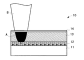
本発明の記録媒体の第1実施形態について説明する。図1は、本発明の記録媒体の第1実施形態とこれに向けて照射されたエネルギービームを示している。図2は、図1中の記録媒体10の一部を拡大して示している。図1中の記録媒体10は、強誘電体の自発分極により情報を保持する記録媒体である。記録媒体10は、例えばハードディスクドライブなどの磁気メモリー、または光ディスクなどの光メモリーと同様に、情報を記録し、保持し、そして記録された情報の読取および再生を実現する情報記録媒体である。しかし、記録媒体10は、記録層の材料として強誘電体を用いており、情報を強誘電体の分極方向として記録し、保持する。このため、理論的には、強誘電体の結晶格子単位まで記録密度を向上させることが可能である。したがって、記録媒体10は、従来の磁気メモリーおよび光メモリーよりも高い記録密度を実現することができる。
(First Embodiment of Recording Medium)
A first embodiment of the recording medium of the present invention will be described. FIG. 1 shows a first embodiment of a recording medium of the present invention and an energy beam irradiated toward the first embodiment. FIG. 2 shows an enlarged part of the
図1に示すように、記録媒体10は、第1導電層11、強誘電体層12、制御層13および第2導電層14を備えている。
As shown in FIG. 1, the
導電層11は、導電層14と共に、強誘電体層12に電圧を印加するための電極として機能する。導電層11は、導電材料から形成されている。例えば、導電層11は、アルミニウム、白金、金、銅またはニッケルなどの金属から形成されている。導電層11は平板形状または薄膜形状に形成されている。導電層11の厚さは特に限定されないが、数10ナノメートル以上の厚さであることが望ましい。なお、導電層11を電極として機能させるだけでなく、記録媒体10の基板として機能させてもよい。この場合には、記録媒体10の強度を大きくするために、導電層11の厚さを厚くする。
The
強誘電体層12は、強誘電体の自発分極により情報を保持する機能を有する。強誘電体層12は、導電層11上に形成されている。強誘電体層12は、強誘電体材料により形成されている。強誘電体材料としては、チタン酸鉛(PbTiO3 )、ジルコン酸鉛(PbZrO3)、チタン酸バリウム(BaTiO3)、ニオブ酸リチウム(LiNbO3 )、タンタル酸リチウム(LiTaO3)等を用いることができる。例えば、結晶面がZ−cutのLiTaO3単結晶は、情報を、記録媒体10の表面と垂直な分極方向として記録する強誘電体材料として適している。強誘電体層12は、薄膜形状に形成されている。強誘電体層12の厚さは、数10ナノメートルないし数100ナノメートルであることが望ましい。
The
情報を強誘電体層12に記録し、保持する原理は、以下のとおりである。すなわち、強誘電体は、その抗電界を超える電界を印加することによって分極方向が変化する性質を有する。また、強誘電体は、電界の印加によって分極方向を変化させると、その後、電界の印加を止めても、その分極方向を維持する性質を有する(自発分極)。これらの性質を利用して、情報を強誘電体層12に記録し、保持する。例えば、強誘電体層12全体の分極方向を、記録媒体10の表面と垂直の一方向(例えば図1に示すように下向き)に予め揃えておく。そして、強誘電体層12に、抗電界を超える電界を、記録媒体10の表面と垂直な方向に、局所的に印加する。これにより、電界を印加した部分の分極方向が反転し、その後、電界の印加を止めても、当該分極方向は反転した状態が維持される。例えば、図1において、記録すべき情報が「0」および「1」からなる2値のデジタルデータである場合には、ビット状態「0」を下向きの分極方向に対応させ、ビット状態「1」を上向きの分極方向に対応させる。この場合には、ビット状態「1」を記録するときに限り、強誘電体層12に電界を印加すればよい。このようにして、情報を強誘電体層12に記録し、保持することができる。
The principle of recording and holding information on the
一方、強誘電体層12に分極方向として記録された情報を再生する原理は、以下のとおりである。すなわち、強誘電体の非線形誘電率は、分極方向によって異なる。この非線形誘電率の相違は、強誘電体に抗電界よりも小さい交番電界を、記録媒体10の表面と垂直な方向に印加し、その状態で、強誘電体の容量変化を検出することにより知ることができる。このときの強誘電体の容量変化は微弱であるが、SNDM方式によれば、これを検出することが可能である。このようにして強誘電体層12の非線形誘電率(容量変化)を検出することにより、強誘電体層12の分極方向を読み取ることができ、情報を再生することができる。
On the other hand, the principle of reproducing information recorded as the polarization direction on the
制御層13は、エネルギービームBの照射により可逆的に導電性が増加する性質を有する。制御層13は、エネルギービームBの照射の有無または強弱によりその導電性を変化させ、導電層11と導電層14との間に供給される電圧の強誘電体層12への印加・遮断を切り換える機能を有する。すなわち、制御層13は、導電層11と導電層14との間に供給される電圧を、エネルギービームBの照射位置に対応する強誘電体層12の一部分(きわめて小さな領域)だけに印加する機能を有する。強誘電体層12への電圧の印加・遮断を切り換える機能を実現するためには、制御層13は、常態では実質的に絶縁体であるが、エネルギービームBの照射により可逆的に導電体となる性質を有していることが望ましい。しかし、常態の制御層13の絶縁性は、導電層11と導電層14との間に供給される電圧の影響が、エネルギービームBの照射位置に対応する強誘電体層12の一部分以外の場所に及ぶのを阻止することができる程度であればよい。また、エネルギービームBの照射時(照射位置)における制御層13の導電性は、導電層11と導電層14との間に供給される電圧が、エネルギービームBの照射位置に対応する強誘電体層12の一部分に印加され、当該電圧印加の所定の目的(例えば記録時の電圧印加であれば分極反転)を達成できる程度であればよい。
The
制御層13は強誘電体層12上に形成されている。制御層13は平板形状または薄膜形状に形成されている。制御層13は、エネルギービームBの照射により可逆的に導電性が増加する材料により形成されている。具体的には、第1実施形態における制御層13は、エネルギービームBの照射により制御層13の温度が上昇することで導電性が増加する材料により形成されている。例えば、制御層13は半導体により形成されている。より具体的には、制御層13は、ポリシリコン、アモルファスシリコンまたはゲルマニウムなどにより形成されている。
The
制御層13の厚さは、エネルギービームBの照射時における導電層11と導電層14との間の電界強度上昇率と、エネルギービームBの照射によって導電性が増加する領域(導電領域A)の勾配G(図2参照)とを考慮して決められる。エネルギービームBの照射時における導電層11と導電層14との間の電界強度上昇率は、「(強誘電体層厚+制御層厚)/強誘電体層厚」である。したがって、電界強度上昇率を大きくするためには、制御層13を厚くすることが望ましい。一方、制御層13が厚いほど、エネルギービームBの照射によって導電性が増加する領域Aの勾配Gが緩やかになる。勾配Gが緩やかになると、エネルギービームBの照射によって導電性が増加する領域Aが広くなり、導電層11と導電層14との間に供給された電圧が強誘電体層12に印加される領域の径D1が大きくなる。この結果、強誘電体層12において、情報の1単位(例えば1ビット)の記録に用いられる領域が大きくなり、情報の記録密度が低下する。そこで、制御層13の厚さは、適度な電界強度上昇率を確保する要請と適度な勾配Gを確保する要請との調和点を探りながら設定することが望ましい。具体的には、制御層13の厚さが、強誘電体層12のおよそ2倍ないし10倍であることが望ましい。
The thickness of the
導電層14は、導電層11と共に、強誘電体層12に電圧を印加するための電極として機能する。導電層14は、制御層13上に形成されている。導電層14は、導電材料から形成されている。例えば、導電層14は、アルミニウム、白金、金、銅またはニッケルなどの金属から形成されている。導電層14は薄膜形状に形成されている。導電層14の厚さは、導電層14の高導電性を確保することと、エネルギービームBの照射により発生する熱の拡散を制限することとを考慮して決められる。導電層14の高導電性を確保するためには、導電層14を超薄膜化するとしても、ある程度の厚みを残すことが望ましい。一方、エネルギービーム照射時の導電層14における熱拡散を制限するためには、導電層14を薄くすることが望ましい。そこで、導電層14の厚さは、高導電性確保の要請と熱拡散制限の要請との調和点を探りながら設定することが望ましい。具体的には、導電層14の厚さは、およそ1ナノメートルないし100ナノメートルであることが望ましい。
The
なお、エネルギービームBは、照射位置における制御層13の温度を上昇させることができるビームであれば何でもよい。例えば、エネルギービームBは、光ビームまたは電子ビームであることが望ましい。
The energy beam B may be any beam that can raise the temperature of the
記録媒体10に情報を記録する原理は以下のとおりである。まず、導電層11と導電層14との間に電圧を供給する。この電圧のレベルは、強誘電体層12の抗電界を超えた電界を作り出すことができる程度に設定される。なお、導電層11と導電層14との間に電圧を供給しただけでは、この電圧は、常態の制御層13の絶縁性により遮断され、強誘電体層12に印加されない。
The principle of recording information on the
続いて、情報を記録すべき位置(記録位置)にエネルギービームBの照射位置を合わせ、エネルギービームBを導電層11の表面に照射する。これにより、エネルギービームBのエネルギーが導電層11を通過して制御層13に伝わり、制御層13の温度が局所的に上昇し、制御層13の導電性が局所的に増加する。この結果、制御層13には、図2に示すような断面形状を有する導電領域Aが形成される。
Subsequently, the irradiation position of the energy beam B is aligned with a position (recording position) where information is to be recorded, and the surface of the
制御層13内に導電領域Aが形成されると、導電層11と導電層14との間に供給された電圧が、導電領域Aを介して強誘電体層12の記録位置に印加される。これにより、強誘電体層12の記録位置における分極方向が局所的に反転する。これは、情報の1単位が強誘電体層12に記録されたことを意味する。
When the conductive region A is formed in the
そして、情報の記録が引き続き行われる場合には、エネルギービームBの照射位置が移動する。これにより、これまでエネルギービームBが照射されていた制御層13の部位においては、エネルギービームBの照射がなくなったことにより、温度が低下し、よって、導電性が低下する。この結果、導電領域Aが消失する。これにより、常態の制御層13の絶縁性が回復するため、導電層11と導電層14との間に供給されている電圧は、制御層13により遮断され、強誘電体層12の当該記録位置に印加されなくなる。そして、エネルギービームBの新たな照射位置では、制御層13内に新たな導電領域が形成され、この新たな導電領域を介して、導電層11と導電層14との間に供給された電圧が、強誘電体層12の新たな記録位置に印加され、これにより、強誘電体層12の新たな記録位置における分極方向が反転する。
When information recording is continued, the irradiation position of the energy beam B moves. Thereby, in the part of the
情報の記録が完了すると、エネルギービームBの照射が止められる。これにより、制御層13内の導電領域は消失し、導電層11と導電層14との間に供給される電圧は、強誘電体層12に印加されなくなる。なお、強誘電体層12に電圧が印加されなくなっても、強誘電体層12に記録された情報は、強誘電体の自発分極の性質により、そのまま保持される。
When the information recording is completed, the irradiation of the energy beam B is stopped. As a result, the conductive region in the
次に、記録媒体10に記録・保持された情報をSNDM方式により再生する原理は、以下のとおりである。まず、導電層11と導電層14との間に交番電圧を供給する。この交番電圧の振幅レベルは、強誘電体層12の抗電界よりも小さい電界を作り出すことができる程度に設定される。
Next, the principle of reproducing information recorded / held in the
続いて、情報を読み取るべき位置(読取位置)にエネルギービームBの照射位置を合わせ、エネルギービームBを導電層11の表面に照射する。これにより、エネルギービームBのエネルギーが導電層11を通過して制御層13に伝わり、制御層13の温度が局所的に上昇し、制御層13の導電性が局所的に増加する。この結果、制御層13には、図2に示すような断面形状を有する導電領域Aが形成される。
Subsequently, the irradiation position of the energy beam B is aligned with the position (reading position) where information is to be read, and the surface of the
制御層13内に導電領域Aが形成されると、導電層11と導電層14との間に供給された交番電圧が、導電領域Aを介して強誘電体層12の読取位置に印加される。これにより、強誘電体層12には、交番電界が作り出され、この電界の交番的変化に伴って、強誘電体層12の容量が変化する。このとき、強誘電体層12の容量変化は、当該読取位置の分極方向が上向きか下向きかによって異なるカーブを描く。これは、当該読取位置の分極方向が上向きか下向きかによって、当該読取位置の非線形誘電率が異なるためである。この容量変化のカーブの相違を電気的に検出することにより、強誘電体層12の当該読取位置の分極方向を知ることができ、よって、当該読取位置に記録された情報を再生することができる。容量変化のカーブの電気的検出は、導電領域Aを介して行う。
When the conductive region A is formed in the
そして、情報の読取が引き続き行われる場合には、エネルギービームBの照射位置が移動する。これにより、これまでエネルギービームBが照射されていた制御層13の部位においては、エネルギービームBの照射がなくなったことにより、温度が低下し、よって、導電性が低下する。この結果、導電領域Aが消失する。これにより、常態の制御層13の絶縁性が回復するため、導電層11と導電層14との間に供給されている交番電圧は、制御層13により遮断され、強誘電体層12の当該読取位置に印加されなくなる。そして、エネルギービームBの新たな照射位置では、制御層13内に新たな導電領域が形成され、この新たな導電領域を介して、導電層11と導電層14との間に供給された交番電圧が、強誘電体層12の新たな読取位置に印加され、これにより、強誘電体層12の新たな読取位置における容量変化が検出される。
Then, when information reading is continued, the irradiation position of the energy beam B moves. Thereby, in the part of the
情報の読取が完了すると、エネルギービームBの照射が止められる。これにより、制御層13内の導電領域は消失し、導電層11と導電層14との間に供給される交番電圧は、強誘電体層12に印加されなくなる。
When the reading of information is completed, the irradiation with the energy beam B is stopped. As a result, the conductive region in the
以上より、記録媒体10は、強誘電体層12に対する電圧印加経路の途中に制御層13を設け、エネルギービームBの照射の有無ないし強弱により制御層13の導電性を変化させる構成を有する。この構成により、エネルギービームBの照射によって制御層13の導電性を局所的に増加させて導電領域Aを形成し、導電領域Aを介して強誘電体層12の記録位置または読取位置に電圧を印加することができる。この導電領域Aは、電圧を記録媒体の強誘電体層(記録層)に局所的に印加する機能を有することなどから、従来のSNDM方式の強誘電体記録におけるプローブと同様の機能を果たす。この点で、導電領域Aを、「疑似プローブ(Virtual Probe)」と呼ぶことができよう。
As described above, the
記録媒体10のかかる構成および作用より、以下のような効果が得られる。まず、記録媒体10によれば、エネルギービームBの照射により記録位置または読取位置を選定することができるため、金属などの固体からなるプローブが不要となる。すなわち、本発明の第1実施形態により、完全非接触型の強誘電体記録媒体を実現することができる。したがって、プローブと記録媒体の表面との接触によるプローブの摩耗・破壊、および記録媒体の摩耗・損傷といった不都合を解消することができる。また、プローブと記録媒体の表面との接触による摩擦がないため、記録媒体に対する情報の記録または再生のための走査を高速化することができる。なお、本明細書において、「完全非接触」とは、情報の記録および読取にあたり、固体のプローブやヘッドを記録媒体に接触させる必要がないだけでなく、固体のプローブやヘッドを記録媒体にきわめて(例えば数ナノないし数十ナノメートル程度の微少な距離をもって)接近させる必要もないことを意味する。
From the configuration and operation of the
次に、記録媒体10によれば、外部から記録媒体10全体に熱を加え、制御層13全体の温度を上昇させ、制御層13全体の導電性を増加させることができる。そして、制御層13全体の導電性を増加させた状態で、導電層11と導電層14との間に、強誘電体層12の抗電界を超える電界を形成することが可能な程度の電圧を印加すれば、強誘電体層12のすべての箇所の分極方向を1方向に揃えることができる。これにより、強誘電体層12に保持されていた情報をすべて消去することができ、記録媒体10を初期化することができる。制御層13全体の導電性を増加させることにより、強誘電体層12全体に一度に電圧を印加することができるので、記録媒体10の初期化を迅速に行うことができる。
Next, according to the
なお、記録媒体10の初期化の方法は、この他にも考えられる。例えば、導電層11と導電層14との間に電圧を供給する。この電圧は、記録時に印加すべき電圧と比較して大幅に大きく、常態の制御層13が非常に大きな抵抗値(記録時において絶縁性を有するといいうるほどの抵抗値)を有するにもかかわらず、強誘電体層12にその抗電界を超える電界を作り出すことができるほどの強度を有する。このような方法によって、記録媒体10の初期化を一度に行うことができ、初期化時間の短縮を図ることができる。また、記録媒体10の初期化のために、導電層11と導電層14との間に比較的大きな電圧を供給すると共に、記録媒体10全体に熱を加えてもよい。これにより、導電層11と導電層14との間に供給する電圧の強度と、記録媒体10に加える熱とを、電圧だけまたは熱だけを加える場合と比較して、それぞれ低くすることができる。
Note that there are other methods for initializing the
次に、記録媒体10によれば、エネルギービームBを照射することにより、制御層13内に導電領域Aを形成する。図2に示すように、導電領域Aは、勾配Gを有しており、勾配Gは、制御層13の厚さまたはエネルギービームBの強度などにより任意に設定することができる。そして、勾配Gを適切に設定することにより、導電領域Aを介して強誘電体層12に電圧が印加される領域の径D1(いわゆる強誘電体層12表面上の記録スポットの径、別言すれば、疑似プローブの先端径)を、エネルギービームの径D2よりも小さくすることができる。したがって、記録密度を向上させることができる。
Next, according to the
次に、上記特許公報(特許文献2)に記載された従来の光メモリーでは、強誘電体薄膜のキュリー点を考慮する必要があるため、用いるべき強誘電体材料の選定が容易でないという問題があった。しかし、本発明の第1実施形態である記録媒体10は、強誘電体層12自体を加熱する構成ではない。したがって、記録媒体10によれば、強誘電体材料を選定するにあたり、強誘電体のキュリー点を考慮する必要はなく、この点で、強誘電体材料の選定が容易になる。
Next, in the conventional optical memory described in the above patent publication (Patent Document 2), it is necessary to consider the Curie point of the ferroelectric thin film, so that there is a problem that it is not easy to select a ferroelectric material to be used. there were. However, the
(記録媒体の第2実施形態)
本発明の記録媒体の第2実施形態について説明する。図3は、本発明の記録媒体の第2実施形態を示している。図3に示すように、記録媒体20は、図1に示す記録媒体10と同様に、導電層11、強誘電体層12および導電層14を備えている。
(Second Embodiment of Recording Medium)
A second embodiment of the recording medium of the present invention will be described. FIG. 3 shows a second embodiment of the recording medium of the present invention. As shown in FIG. 3, the
記録媒体20の制御層21は、記録媒体10の制御層13と同様に、エネルギービームBの照射により可逆的に導電性が増加する性質を有し、エネルギービームBの照射の有無または強弱によりその導電性を変化させ、導電層11と導電層14との間に供給される電圧の強誘電体層12への印加・遮断を切り換える機能を有する。ところが、制御層21は、制御層13と異なり、エネルギービームBの照射により当該制御層21中に熱非平衡状態のキャリアが発生することで導電性が増加する材料から形成されている。具体的には、制御層21は、電子倍増現象(電子雪崩現象)を起こす性質を有する材料から形成されており、例えば、セレン、ゲルマニウム、ガリウムヒ素(GaAs)、またはガリウムりん(GaP)などにより形成されている。
Similar to the
このような構成を有する記録媒体20によっても、上述した記録媒体10とほぼ同様の効果を得ることができる。
Even with the
(記録媒体の他の実施形態)
本発明の記録媒体においては、エネルギービームの照射により、制御層の導電性を局所的に増加させ、その部分に導電領域(疑似プローブ)を形成する。図1に示す記録媒体10では、エネルギービームBの照射により制御層13の温度を局所的に上昇させることにより導電領域Aを形成する。また、図3に示す記録媒体20では、エネルギービームBの照射により制御層21中に熱非平衡状態のキャリアを発生させることで導電領域Aを形成する。しかし、本発明はこれらに限られない。例えば、エネルギービームの照射により制御層中に電子密度勾配を形成することにより導電領域を形成してもよい。具体的には、エネルギービームが照射される側に位置する導電層をようやく電子が移動する程度の薄さに形成し、制御層をこの導電層よりもやや導電率の低い半導体(例えばシリコンまたはゲルマニウムなど)により形成する。これにより、制御層内において、エネルギービームが照射されたスポットを中心に電子密度勾配を形成することができる。そして、この電子密度勾配はエネルギービームの移動により移動させることができる。
(Other Embodiments of Recording Medium)
In the recording medium of the present invention, the conductivity of the control layer is locally increased by irradiation with an energy beam, and a conductive region (pseudo probe) is formed in that portion. In the
一方、図1および図2に示す記録媒体10では、導電領域Aの勾配Gを、制御層13の厚さまたはエネルギービームBの強度などにより適切に設定することにより、導電領域Aを介して強誘電体層12に電圧が印加される領域の径D1(すなわち、疑似プローブの先端径)を小さくし、記録密度の向上を図っている。しかし、径D1を小さくする方法は、これに限られない。例えば、制御層を、熱伝導異方性または電気伝導異方性を有する材料(例えばシリコンなど)により形成し、エネルギービームの照射により制御層内に形成される導電領域の断面形状を、記録媒体の表面に垂直な方向に細長い形状となるようにしてもよい。
On the other hand, in the
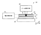
(記録装置の実施形態)
本発明の記録装置の実施形態について説明する。図4は、本発明の記録装置の実施形態を、記録媒体と共に示している。図4中の記録装置30は、上述した記録媒体10、記録媒体20その他、本発明の記録媒体に情報を記録する装置である。記録装置30は、例えば、ハードディスクドライブ、光ディスクドライブなどと同様に、コンピュータ、オーディオ・ビデオレコーダ、制御機器、医療機器など、様々な機器に用いることができる。なお、説明の便宜のため、以下、記録装置30により記録媒体10に情報を記録する場合を例に挙げる。
(Embodiment of recording apparatus)
An embodiment of a recording apparatus of the present invention will be described. FIG. 4 shows an embodiment of the recording apparatus of the present invention together with a recording medium. A
図4に示すように、記録装置30は、電圧供給手段31、ビーム照射手段32および照射位置制御手段33を備えている。
As shown in FIG. 4, the
電圧供給手段31は、記録媒体10の導電層11と導電層14との間に強誘電体層12の分極方向を設定するための電圧を供給する。電圧供給手段31は、強誘電体層12の抗電界を超える電界を形成し得る程度の強度を有する電圧を供給することができる。電圧供給手段31は、例えば、直流電圧発生回路またはパルス電圧発生回路、および増幅回路などにより実現することができる。
The
ビーム照射手段32は、例えば光ビームまたは電子ビームといったエネルギービームBを記録媒体10に照射する。ビーム照射手段32は、エネルギービームBが光ビームの場合には、例えば半導体レーザおよびレンズその他の光学システムなどにより実現することができる。また、ビーム照射手段32は、エネルギービームBが電子ビームの場合には、例えば電子銃などを備えた電子ビーム装置などにより実現することができる。
The
照射位置制御手段33は、記録媒体10に対するエネルギービームBの照射位置を記録媒体10の表面と平行な方向に移動させる。記録媒体10に対するエネルギービームBの照射位置を移動させるには、エネルギービームBがビーム照射手段32から記録媒体10に至る照射経路を固定しつつ記録媒体10を移動させる方法と、記録媒体10を固定しつつエネルギービームBの照射経路を移動させる方法が考えられる。照射位置制御手段は、いずれの方法によっても実現することができる。図4に示す照射位置制御手段33は、エネルギービームBの照射経路を固定しつつ記録媒体10を移動させる方法を採用している。例えば、照射位置制御手段33は、X−Yステージであり、ステージ上に載置された記録媒体10を、記録媒体10の表面に平行なX方向およびY方向に移動させることができる。
The irradiation position control means 33 moves the irradiation position of the energy beam B on the
記録装置30の動作は、以下のとおりである。情報を記録媒体10に記録するとき、まず、照射位置制御手段33は、記録媒体10をX方向、Y方向に移動させ、エネルギービームBの照射位置を、記録媒体10における情報を記録すべき位置(記録位置)に一致させる。続いて、電圧供給手段31は、記録媒体10の導電層11と導電層14との間に強誘電体層12の分極方向を設定するための電圧を供給する。また、ビーム照射手段32は、エネルギービームBを記録媒体10に照射する。これにより、記録媒体10において、エネルギービームBの照射位置に導電領域A(疑似プローブ)が形成され、導電層11および14間に供給された電圧が導電領域Aを介して強誘電体層12の当該記録位置に印加され、当該記録位置の分極方向が反転し、よって情報が記録される。
The operation of the
以上より、記録装置30によれば、エネルギービームBの照射によって記録媒体10の制御層13内に導電領域A(疑似プローブ)を形成し、これにより、強誘電体層12における情報の記録位置を選定することができる。したがって、記録装置30によれば、完全非接触型の強誘電体記録を実現することができる。このため、固体のプローブが不要となり、プローブと記録媒体との接触または摩擦によるプローブの摩耗・破壊、記録媒体の表面の摩耗・損傷といった問題は生じない。したがって、記録装置30によれば、耐久性に優れ、かつ長寿命の記録装置を実現することができる。また、固体プローブと記録媒体との接触がないため、記録媒体に対する情報の記録のための走査を高速化することができる。
As described above, according to the
(記録装置の実施形態の各種態様)
本発明の記録装置の各種態様について説明する。記録装置30では、記録媒体10に対し、電圧供給手段31による電圧の供給と、ビーム照射手段32によるエネルギービームBの照射とを同時に(いっしょに)行うことにより、情報を記録媒体10に記録する。このような記録方法には、2つの方法が考えられる。すなわち、第1の方法は、電圧供給手段31により導電層11および14間に電圧を連続的に供給した状態で、ビーム照射手段32から、記録すべき情報によって変調されたエネルギービームBを照射する方法である。第2の方法は、ビーム照射手段32により記録媒体10にエネルギービームBを連続的に照射した状態で、電圧供給手段31から導電層11および14間に、記録すべき情報によって変調された電圧を供給する方法である。
(Various aspects of the embodiment of the recording apparatus)
Various aspects of the recording apparatus of the present invention will be described. In the
図5は、第1の方法を採用した記録装置30の一態様を示している。この態様では、記録装置30は、記録媒体10に記録すべき情報に対応してエネルギービームBの照射の有無または強弱を制御するビーム制御手段34を備えている。
FIG. 5 shows an aspect of the
例えば、記録媒体10(強誘電体層12)において、記録媒体10の表面に平行な直線方向に連続的に並ぶ複数の記録位置(例えば直線状のトラック上に連続的に並ぶ複数の記録位置)に、2値のデジタルデータを連続的に記録する場合を想定する。この場合、記録装置30において、まず、照射位置制御手段33は、記録媒体10をX方向、Y方向に移動させ、エネルギービームBの照射位置を、記録媒体10における記録開始位置に一致させる。続いて、電圧供給手段31は、記録媒体10の導電層11と導電層14との間に電圧を供給する。そして、ビーム照射手段32は、エネルギービームBの照射を開始する。続いて、照射位置制御手段33は、記録媒体10を例えばX方向に所定の速度で直線的に移動させる。これと同時に、ビーム制御手段34は、記録すべきデジタルデータに基づいてエネルギービームBを変調する。例えば、記録すべきデジタルデータのビット状態が「0」のときには、エネルギービームBを一時的に停止し、またはエネルギービーBの強度を一時的に弱める。また、記録すべきデジタルデータのビット状態が「1」のときには、エネルギービームBの強度を維持しまたは一時的に強める。これにより、2値のデジタルデータが記録媒体10(強誘電体層12)に連続的に記録される。なお、ビーム制御手段34は、信号処理回路などにより実現することができる。
For example, in the recording medium 10 (ferroelectric layer 12), a plurality of recording positions continuously arranged in a linear direction parallel to the surface of the recording medium 10 (for example, a plurality of recording positions continuously arranged on a linear track). Assume that binary digital data is continuously recorded. In this case, in the
図6は、第2の方法を採用した記録装置30の一態様を示している。この態様では、記録装置30は、記録媒体10に記録すべき情報に対応して電圧の供給の有無または強弱を制御する電圧制御手段35を備えている。
FIG. 6 shows an aspect of the
例えば、記録媒体10(強誘電体層12)において、記録媒体10の表面に平行な直線方向に連続的に並ぶ複数の記録位置に、2値のデジタルデータを連続的に記録する場合を想定する。この場合、記録装置30において、まず、照射位置制御手段33は、記録媒体10をX方向、Y方向に移動させ、エネルギービームBの照射位置を、記録媒体10における記録開始位置に一致させる。そして、ビーム照射手段32は、エネルギービームBの照射を開始する。続いて、電圧供給手段31は、記録媒体10の導電層11と導電層14との間に電圧(記録電圧)を供給する。続いて、照射位置制御手段33は、記録媒体10を例えばX方向に所定の速度で直線的に移動させる。これと同時に、電圧制御手段35は、記録すべきデジタルデータに基づいて記録電圧を変調する。例えば、記録すべきデジタルデータのビット状態が「0」のときには、記録電圧を一時的にゼロにし、または記録電圧を一時的に小さくする。また、記録すべきデジタルデータのビット状態が「1」のときには、記録電圧の強度を維持しまたは一時的に大きくする。これにより、2値のデジタルデータが記録媒体10(強誘電体層12)に連続的に記録される。なお、電圧制御手段35は、信号処理回路などにより実現することができる。
For example, assume that binary digital data is continuously recorded at a plurality of recording positions continuously arranged in a linear direction parallel to the surface of the
(再生装置の実施形態)
本発明の再生装置の実施形態について説明する。図7は、本発明の再生装置の実施形態を、記録媒体と共に示している。図7中の再生装置40は、上述した記録媒体10、記録媒体20その他、本発明の記録媒体に保持された情報を再生する装置である。再生装置40は、例えば、ハードディスクドライブ、光ディスクドライブなどと同様に、コンピュータ、オーディオ・ビデオプレーヤ、制御機器、医療機器など、様々な機器に用いることができる。なお、説明の便宜のため、以下、再生装置40により記録媒体10に保持された情報をSNDM方式により再生する場合を例に挙げる。
(Embodiment of playback device)
An embodiment of the playback apparatus of the present invention will be described. FIG. 7 shows an embodiment of the reproducing apparatus of the present invention together with a recording medium. A
図7に示すように、再生装置40は、電圧供給手段41、ビーム照射手段42、検出手段43および照射位置制御手段44を備えている。
As shown in FIG. 7, the reproducing
電圧供給手段41は、記録媒体10の導電層11と導電層14との間に電圧を供給する。記録媒体10において、情報は強誘電体層12の分極方向として保持されている。そして、強誘電体層12の分極方向は、強誘電体層12の非線形誘電率を検出することにより知ることができる。さらに、強誘電体層12の非線形誘電率は、強誘電体層12に、その抗電界よりも小さい電界(以下、これを「検出用電界」という。)を印加した状態で、強誘電体層12の容量を検出することにより知ることができる。電圧供給手段41が記録媒体10の導電層11と導電層14との間に供給する電圧は、検出用電界を作り出すためのものである。検出用電界は、交番電界であることが望ましい。したがって、電圧供給手段41により供給すべき電圧は交番電圧であることが望ましい。電圧供給手段41は、例えば、交流電源および増幅回路などにより実現することができる。
The
なお、SNDM方式には、検出用電界として、交番電界を用いる方式と、直流電界を用いる方式がある。上述した各実施形態および上述する実施例では、検出用電界として交番電界を用いる方式を採用した場合を例に挙げている。しかし、本発明は、検出用電界として直流電界を用いる場合にも適用することができる。この場合には、電圧供給手段41により供給すべき電圧を直流電圧とする。そして、この場合には、電圧供給手段41を直流電源および増幅回路などにより実現することができる。 The SNDM method includes a method using an alternating electric field and a method using a DC electric field as a detection electric field. In each of the above-described embodiments and the above-described examples, a case where a system using an alternating electric field as a detection electric field is employed is taken as an example. However, the present invention can also be applied when a DC electric field is used as the detection electric field. In this case, the voltage to be supplied by the voltage supply means 41 is a DC voltage. In this case, the voltage supply means 41 can be realized by a DC power supply and an amplifier circuit.
ビーム照射手段42は、例えば光ビームまたは電子ビームといったエネルギービームBを記録媒体10に照射する。ビーム照射手段42は、エネルギービームBが光ビームの場合には、例えば半導体レーザおよびレンズその他の光学システムなどにより実現することができる。また、ビーム照射手段42は、エネルギービームBが電子ビームの場合には、例えば電子銃などを備えた電子ビーム装置などにより実現することができる。
The
検出手段43は、記録媒体10の強誘電体層12の分極方向を検出する。強誘電体層12の分極方向は、強誘電体層12の非線形誘電率を検出することにより検出することができる。そのため、検出手段43には、強誘電体層12の非線形誘電率を検出するための非線形誘電率検出手段を備えることが望ましい。より具体的に説明すると、強誘電体層12の非線形誘電率は、強誘電体層12に抗電界よりも小さい交番電界を印加し、その状態で、強誘電体層12の容量変化を検出することにより知ることができる。そのため、検出手段43は、非線形誘電率検出手段として、強誘電体層12の容量変化を検出する手段を備えることが望ましい。上記特開2003−085969号公報(特許文献1)には、強誘電体層12に交番電界を印加し、強誘電体層12の容量変化に対応する周波数変調信号を作り出し、これに基づいて強誘電体層12の容量変化を検出する手段が記載されている。検出手段43は、これとほぼ同様の手段により実現することができる(もっとも、本発明の実施形態である再生装置40には、固体プローブではなく、エネルギービームBの照射により制御層13内に形成される疑似プローブが用いられる)。
The detecting means 43 detects the polarization direction of the
照射位置制御手段44は、記録媒体10に対するエネルギービームBの照射位置を記録媒体10の表面と平行な方向に移動させる。記録媒体10に対するエネルギービームBの照射位置を移動させるには、エネルギービームBがビーム照射手段42から記録媒体10に至る照射経路を固定しつつ記録媒体10を移動させる方法と、記録媒体10を固定しつつエネルギービームBの照射経路を移動させる方法が考えられる。照射位置制御手段は、いずれの方法によっても実現することができる。図7に示す照射位置制御手段44は、エネルギービームBの照射経路を固定しつつ記録媒体10を移動させる方法を採用している。例えば、照射位置制御手段44は、X−Yステージであり、ステージ上に載置された記録媒体10を図7中のX方向およびY方向に移動させることができる。
The irradiation position control means 44 moves the irradiation position of the energy beam B on the
再生装置40の動作は、以下のとおりである。記録媒体10に保持された情報を再生するとき、まず、照射位置制御手段44は、記録媒体10をX方向、Y方向に移動させ、エネルギービームBの照射位置を、記録媒体10において再生すべき情報が保持されている位置(読取位置)に一致させる。続いて、電圧供給手段41は、記録媒体10の導電層11と導電層14との間に交番電圧を供給する。また、ビーム照射手段42は、エネルギービームBを記録媒体10に照射する。これにより、記録媒体10において、エネルギービームBの照射位置に導電領域A(疑似プローブ)が形成され、導電層11および14間に供給された交番電圧が導電領域Aを介して強誘電体層12の当該読取位置に印加される。さらに、導電領域Aを介して、強誘電体層12の当該読取位置と検出手段43とが電気的に接続される。続いて、検出手段43は、強誘電体層12の当該読取位置の容量変化を検出する。この容量変化に基づいて、当該読取位置に保持されている情報が再生される。
The operation of the
以上より、再生装置40によれば、エネルギービームBの照射によって記録媒体10の制御層13内に導電領域A(疑似プローブ)を形成し、これにより、強誘電体層12における情報の読取位置を選定することができる。したがって、再生装置40によれば、強誘電体記録媒体において完全非接触型の情報再生を実現することができる。このため、固体のプローブが不要となり、プローブと記録媒体との接触または摩擦によるプローブの摩耗・破壊、記録媒体の表面の摩耗・損傷といった問題は生じない。したがって、再生装置40によれば、耐久性に優れ、かつ長寿命の再生装置を実現することができる。また、固体プローブと記録媒体との接触がないため、記録媒体に対する情報の読取のための走査を高速化することができる。
As described above, according to the reproducing
なお、以上のような記録装置および再生装置の実施形態は、専用の装置としてハードウェアと一体的に構成する形態で実現してもよいし、ハードウェアとソフトウェア(コンピュータプログラム)との組合せにより実現してもよい。 Note that the above-described embodiments of the recording device and the reproducing device may be realized as a dedicated device configured integrally with hardware, or realized by a combination of hardware and software (computer program). May be.
以下、本発明の記録装置および再生装置の実施例について図面を参照しながら説明する。図8は、本発明の記録装置および再生装置の実施例である記録再生装置を示している。図8中の記録再生装置50は、上述した記録媒体10(図1参照)に対して情報を記録する機能と、記録媒体10に保持された情報を再生する機能を有している。
Hereinafter, embodiments of a recording apparatus and a reproducing apparatus of the present invention will be described with reference to the drawings. FIG. 8 shows a recording / reproducing apparatus which is an embodiment of the recording apparatus and the reproducing apparatus of the present invention. A recording / reproducing
記録再生装置50は、記録信号生成回路51、交番電圧源52、光ビームユニット53、発振回路54、信号処理回路55、X−Yステージ56および切換スイッチ57を備えている。
The recording / reproducing
記録再生装置50の記録機能は、記録信号生成回路51、光ビームユニット53およびX−Yステージ56により実現される。記録信号生成回路51は、記録媒体10に記録すべき情報に対応する記録パルス信号を生成し、これを記録媒体10の導電層11および14間に供給する回路である。記録パルス信号の振幅は、当該記録パルス信号を記録媒体10の強誘電体層12に印加したときに、強誘電体層12中にその抗電界を超える程度の電界を形成し得る程度の大きさを有する。記録信号生成回路51は、パルス信号生成回路および増幅回路などにより構成されている。光ビームユニット53は、記録媒体10に向けて光ビームLを照射する装置である。光ビームユニット53は、半導体レーザ、レンズおよびミラーなどにより構成されている。X−Yステージ56は、その上に記録媒体10を載置し、記録媒体10をその表面と平行なX方向およびY方向に移動させる機構である。記録信号生成回路51、光ビームユニット53およびX−Yステージ56は、記録再生装置50の動作を制御するコントローラ(図示せず)にそれぞれ電気的に接続されており、コントローラにより、パルス信号の出力タイミング、光ビームの照射タイミング、および記録媒体10の移動などが制御される。
The recording function of the recording / reproducing
記録媒体10に情報を記録するとき、記録再生装置50は、以下のように動作する。まず、コントローラの制御に基づき、切換スイッチ57は、記録信号生成回路51と記録媒体10の導電層14との間を電気的に接続する。続いて、X−Yステージ56は、記録媒体10をX方向、Y方向に移動させ、光ビームLの照射位置を、記録媒体10における情報を記録すべき位置(記録位置)に一致させる。続いて、記録信号生成回路51は、記録媒体10の導電層11と導電層14との間に記録パルス信号を供給する。これと同時に、光ビームユニット53は、光ビームLを記録媒体10に照射する。これにより、記録媒体10において、光ビームLの照射位置に導電領域(疑似プローブ)が形成され、導電層11および14間に供給された電圧が導電領域を介して強誘電体層12の当該記録位置に印加され、当該記録位置の分極方向が反転し、よって情報が記録される。
When recording information on the
記録再生装置50はSNDM方式を採用している。記録再生装置50の再生機能は、交番電圧源52、光ビームユニット53、発振回路54、信号処理回路55およびX−Yステージ56により実現される。交番電圧源52は、記録媒体10の導電層11および14間に交番電圧を供給する。交番電圧の振幅は、当該交番電圧を記録媒体10の強誘電体層12に印加したときに、強誘電体層12中にその抗電界よりも小さな交番電界を形成し得る程度の大きさを有する。また、交番電圧の周波数は、例えば5kHz程度である。発振回路54は、強誘電体層12の容量変化によって周波数が変化する高周波信号を出力する回路である。この高周波信号の平均的な周波数は、例えば1GHz程度である。具体的には、発振回路54は、インダクタを有し、このインダクタのインダクタンスと強誘電体層12の容量とでLC共振回路を形成するように構成されている。信号処理回路55は、発振回路54から出力された高周波信号の周波数変化を電圧変化に変換し、その電圧変化に基づいて強誘電体層12の非線形誘電率(分極方向)を検出する回路である。信号処理回路55は、周波数−電圧変換回路および検波回路などから構成されている。より具体的には、信号処理回路55は、FM復調回路およびロックインアンプなどにより構成されている。交番電圧源52、発振回路54および信号処理回路55も、記録再生装置50の動作を制御するコントローラにそれぞれ接続されており、コントローラの制御に従って動作する。
The recording / reproducing
記録媒体10に保持された情報を再生するとき、記録再生装置50は以下のように動作する。まず、コントローラの制御に基づき、切換スイッチ57は、交番電圧源52と記録媒体10の導電層14との間を電気的に接続する。続いて、X−Yステージ56は、記録媒体10をX方向、Y方向に移動させ、光ビームLの照射位置を、記録媒体10において再生すべき情報が保持されている位置(読取位置)に一致させる。続いて、交番電圧源52は、記録媒体10の導電層11と導電層14との間に交番電圧を供給する。これと同時に、光ビームユニット53は、光ビームLを記録媒体10に照射する。これにより、記録媒体10において、光ビームLの照射位置に導電領域(疑似プローブ)が形成され、導電層11および14間に供給された交番電圧が導電領域を介して強誘電体層12の当該読取位置に印加される。この結果、強誘電体層12の当該読取位置に交番電界が形成され、この交番電界に従って、当該読取位置における強誘電体層12の容量が交番的に変化する。さらに、導電領域を介して、強誘電体層12の当該読取位置と発振回路54とが電気的に接続される。続いて、発振回路54は、強誘電体層12の当該読取位置の容量変化に対応して周波数が変化する高周波信号を出力する。続いて、信号処理回路55は、発振回路54から出力された高周波信号の周波数変化を電圧変化に変換し、この電圧変化について検波を行い、情報を再生する。
When reproducing the information held in the
なお、本発明は、請求の範囲および明細書全体から読み取るこのできる発明の要旨または思想に反しない範囲で適宜変更可能であり、そのような変更を伴う記録媒体、記録装置および再生装置もまた本発明の技術思想に含まれる。 It should be noted that the present invention can be appropriately changed without departing from the gist or concept of the invention that can be read from the claims and the entire specification, and a recording medium, a recording apparatus, and a reproducing apparatus that involve such a change are also included in the present invention. It is included in the technical idea of the invention.
10、20…記録媒体
11、14…導電層
12…強誘電体層
14、21…制御層
30…記録装置
31…電圧供給手段
32…ビーム照射手段
40…再生装置
41…電圧供給手段
42…ビーム照射手段
43…検出手段
50…記録再生装置
51…記録信号生成回路(電圧供給手段)
52…交番電圧源(交番電圧供給手段)
53…光ビームユニット(ビーム照射手段)
54…発振回路(容量検出手段)
55…信号処理回路(信号処理手段)
DESCRIPTION OF
52 ... Alternating voltage source (alternating voltage supply means)
53. Light beam unit (beam irradiation means)
54. Oscillation circuit (capacitance detection means)
55. Signal processing circuit (signal processing means)
Claims (17)
第1導電層と、
前記第1導電層上に形成され、自発分極により前記情報を保持する強誘電体層と、
前記強誘電体層上に形成され、エネルギービームの照射により可逆的に導電性が増加する制御層と、
前記制御層上に形成された第2導電層と
を備え、
前記制御層の厚さは、前記エネルギービームの照射時における前記第1導電層と前記第2導電層との間の電界強度上昇率、および、当該制御層のうち前記エネルギービームの照射によって導電性が増加する領域の勾配のうち少なくとも一方に基づいて定められていることを特徴とする記録媒体。 A recording medium that retains information by spontaneous polarization of a ferroelectric,
A first conductive layer;
A ferroelectric layer formed on the first conductive layer and retaining the information by spontaneous polarization;
A control layer formed on the ferroelectric layer and reversibly increasing conductivity by irradiation of an energy beam;
A second conductive layer formed on the control layer ,
The thickness of the control layer is determined by the rate of increase in the electric field strength between the first conductive layer and the second conductive layer during irradiation of the energy beam, and the conductivity of the control layer by irradiation of the energy beam. A recording medium characterized in that it is determined based on at least one of the gradients of the region in which increases .
前記第1導電層と前記第2導電層との間に前記強誘電体層の分極方向を設定するための電圧を供給する電圧供給手段と、
前記記録媒体に前記エネルギービームを照射するビーム照射手段と、
前記記録媒体に対する前記エネルギービームの照射位置を前記記録媒体の表面と平行な方向に移動させる照射位置制御手段と
を備えていることを特徴とする記録装置。 A first conductive layer, a ferroelectric layer formed on the first conductive layer and retaining information by spontaneous polarization, and formed on the ferroelectric layer and reversibly increased by irradiation with an energy beam. A control layer; and a second conductive layer formed on the control layer, wherein the thickness of the control layer is between the first conductive layer and the second conductive layer when the energy beam is irradiated. A recording apparatus for recording information on a recording medium determined based on at least one of an electric field strength increase rate and a gradient of a region where conductivity is increased by irradiation of the energy beam in the control layer ,
Voltage supply means for supplying a voltage for setting a polarization direction of the ferroelectric layer between the first conductive layer and the second conductive layer;
Beam irradiation means for irradiating the recording medium with the energy beam;
A recording apparatus comprising: an irradiation position control means for moving the irradiation position of the energy beam on the recording medium in a direction parallel to the surface of the recording medium.
前記第1導電層と前記第2導電層との間に電圧を供給する電圧供給手段と、
前記記録媒体に前記エネルギービームを照射するビーム照射手段と、
前記強誘電体層の分極方向を検出する検出手段と、
前記記録媒体に対する前記エネルギービームの照射位置を前記記録媒体の表面と平行な方向に移動させる照射位置制御手段と
を備えていることを特徴とする再生装置。 A first conductive layer, a ferroelectric layer formed on the first conductive layer and retaining information by spontaneous polarization, and formed on the ferroelectric layer and reversibly increased by irradiation with an energy beam. A playback device for playing back information held on a recording medium comprising a control layer and a second conductive layer formed on the control layer,
Voltage supply means for supplying a voltage between the first conductive layer and the second conductive layer;
Beam irradiation means for irradiating the recording medium with the energy beam;
Detection means for detecting the polarization direction of the ferroelectric layer;
A reproducing apparatus comprising: an irradiation position control means for moving the irradiation position of the energy beam on the recording medium in a direction parallel to the surface of the recording medium.
前記検出手段は、
前記交番電圧供給手段による前記交番電圧の供給および前記ビーム照射手段による前記エネルギービームの照射によって前記強誘電体層に交番電界が形成されたとき、この交番電界によって生じる前記強誘電体層の容量変化を検出する容量検出手段と、
前記容量検出手段により検出された前記強誘電体層の容量変化に基づいて前記強誘電体層の自発分極によって保持された情報を再生する信号処理手段と
を備えていることを特徴とする請求項13に記載の再生装置。 The voltage supply means includes an alternating voltage supply means for supplying an alternating voltage between the first conductive layer and the second conductive layer,
The detection means includes
When an alternating electric field is formed in the ferroelectric layer by the supply of the alternating voltage by the alternating voltage supply means and the irradiation of the energy beam by the beam irradiation means, the capacitance change of the ferroelectric layer caused by the alternating electric field Capacity detecting means for detecting
2. A signal processing unit for reproducing information held by spontaneous polarization of the ferroelectric layer based on a change in capacitance of the ferroelectric layer detected by the capacitance detection unit. 14. The playback device according to 13.
Priority Applications (2)
| Application Number | Priority Date | Filing Date | Title |
|---|---|---|---|
| JP2004015891A JP4017118B2 (en) | 2004-01-23 | 2004-01-23 | Recording medium, recording apparatus and reproducing apparatus using ferroelectric substance |
| US11/038,497 US20050163021A1 (en) | 2004-01-23 | 2005-01-21 | Recording medium using ferroelectric substance, recording apparatus and reproducing apparatus |
Applications Claiming Priority (1)
| Application Number | Priority Date | Filing Date | Title |
|---|---|---|---|
| JP2004015891A JP4017118B2 (en) | 2004-01-23 | 2004-01-23 | Recording medium, recording apparatus and reproducing apparatus using ferroelectric substance |
Publications (3)
| Publication Number | Publication Date |
|---|---|
| JP2005209300A JP2005209300A (en) | 2005-08-04 |
| JP2005209300A5 JP2005209300A5 (en) | 2006-05-25 |
| JP4017118B2 true JP4017118B2 (en) | 2007-12-05 |
Family
ID=34792458
Family Applications (1)
| Application Number | Title | Priority Date | Filing Date |
|---|---|---|---|
| JP2004015891A Expired - Fee Related JP4017118B2 (en) | 2004-01-23 | 2004-01-23 | Recording medium, recording apparatus and reproducing apparatus using ferroelectric substance |
Country Status (2)
| Country | Link |
|---|---|
| US (1) | US20050163021A1 (en) |
| JP (1) | JP4017118B2 (en) |
Families Citing this family (6)
| Publication number | Priority date | Publication date | Assignee | Title |
|---|---|---|---|---|
| US6690602B1 (en) * | 2002-04-08 | 2004-02-10 | Advanced Micro Devices, Inc. | Algorithm dynamic reference programming |
| US6700815B2 (en) * | 2002-04-08 | 2004-03-02 | Advanced Micro Devices, Inc. | Refresh scheme for dynamic page programming |
| KR100590564B1 (en) | 2004-10-29 | 2006-06-19 | 삼성전자주식회사 | Ferroelectric recording medium comprising anisotropic conduction layer, recording apparatus comprising the same, and recording method of the same |
| US7782741B2 (en) * | 2007-01-18 | 2010-08-24 | Seagate Technology Llc | Probe-scanned ferroelectric media with imprinted regions |
| RU171070U1 (en) * | 2016-06-28 | 2017-05-18 | Федеральное государственное бюджетное образовательное учреждение высшего образования "Московский технологический университет" | DEVICE FOR RECORDING INFORMATION ON A FERROELECTRIC MEDIA |
| US11087791B1 (en) * | 2020-05-05 | 2021-08-10 | Western Digital Technologies, Inc. | Data storage device with voltage-assisted magnetic recording (VAMR) for high density magnetic recording |
Family Cites Families (5)
| Publication number | Priority date | Publication date | Assignee | Title |
|---|---|---|---|---|
| JP2890011B2 (en) * | 1992-08-19 | 1999-05-10 | 富士写真フイルム株式会社 | Information recording method |
| JPH09120593A (en) * | 1995-08-23 | 1997-05-06 | Sony Corp | Recording and reproducing device |
| JP4771324B2 (en) * | 2001-09-10 | 2011-09-14 | パイオニア株式会社 | Dielectric information apparatus, tape-shaped medium recording / reproducing apparatus, and disk-shaped medium recording / reproducing apparatus |
| US7379412B2 (en) * | 2004-04-16 | 2008-05-27 | Nanochip, Inc. | Methods for writing and reading highly resolved domains for high density data storage |
| KR100590564B1 (en) * | 2004-10-29 | 2006-06-19 | 삼성전자주식회사 | Ferroelectric recording medium comprising anisotropic conduction layer, recording apparatus comprising the same, and recording method of the same |
-
2004
- 2004-01-23 JP JP2004015891A patent/JP4017118B2/en not_active Expired - Fee Related
-
2005
- 2005-01-21 US US11/038,497 patent/US20050163021A1/en not_active Abandoned
Also Published As
| Publication number | Publication date |
|---|---|
| JP2005209300A (en) | 2005-08-04 |
| US20050163021A1 (en) | 2005-07-28 |
Similar Documents
| Publication | Publication Date | Title |
|---|---|---|
| JP4274571B2 (en) | Recording / reproducing head and recording / reproducing apparatus | |
| JP3701268B2 (en) | Dielectric recording apparatus, dielectric reproducing apparatus, and dielectric recording / reproducing apparatus | |
| JP3954457B2 (en) | Dielectric recording medium and dielectric recording / reproducing apparatus | |
| US20050163021A1 (en) | Recording medium using ferroelectric substance, recording apparatus and reproducing apparatus | |
| JPH01133239A (en) | Information recording and reproducing system and information recording medium | |
| KR100537498B1 (en) | High density information storage apparatus using electron emission and methods for writing, reading and erasing using the same | |
| JP4328355B2 (en) | Information reproducing apparatus for ferroelectric recording medium | |
| JP5400731B2 (en) | Magnetic recording medium, magnetic reproducing apparatus, and magnetic reproducing method | |
| WO2023189452A1 (en) | Dielectric reproduction device and dielectric recording and reproduction device | |
| JP2006268894A (en) | Dielectric recording/reproducing device, recording method, and electrode therefor | |
| JP2790716B2 (en) | Magneto-optical recording device | |
| KR100519772B1 (en) | Magnetic medium using spin-polarized electron and Apparatus of recording data and Recording method using the same | |
| JP2968610B2 (en) | Information recording / reproducing device | |
| JP4572756B2 (en) | Recording method to ferroelectric layer and recording device to ferroelectric layer | |
| JPH06236585A (en) | Information recording and reproducing method | |
| JP2009134852A (en) | Nano probe heating apparatus and heat auxiliary magnetic recording head using the same | |
| JPH0453003A (en) | Magneto-optical reproducing device | |
| JPH10172188A (en) | Information recording method and information recorder | |
| JPH1196609A (en) | Magneto-optical information reproducing device | |
| JP2004253044A (en) | Optically assisted magnetic recording disk drive and optically assisted magnetic recording disk | |
| JPH02249158A (en) | Recording and reproducing device | |
| JP2007066495A (en) | Ferroelectric information storage system, and method of storing/reproducing information | |
| JPH01179246A (en) | Magneto-optical recording and reproducing device | |
| KR20000042134A (en) | Optical magnetic recording medium and playback method thereof | |
| JPS61178750A (en) | Method and device for optomagnetic recording, reproducing and erasing |
Legal Events
| Date | Code | Title | Description |
|---|---|---|---|
| A521 | Written amendment |
Free format text: JAPANESE INTERMEDIATE CODE: A523 Effective date: 20060329 |
|
| A621 | Written request for application examination |
Free format text: JAPANESE INTERMEDIATE CODE: A621 Effective date: 20060329 |
|
| A131 | Notification of reasons for refusal |
Free format text: JAPANESE INTERMEDIATE CODE: A131 Effective date: 20070206 |
|
| A521 | Written amendment |
Free format text: JAPANESE INTERMEDIATE CODE: A523 Effective date: 20070405 |
|
| TRDD | Decision of grant or rejection written | ||
| A01 | Written decision to grant a patent or to grant a registration (utility model) |
Free format text: JAPANESE INTERMEDIATE CODE: A01 Effective date: 20070904 |
|
| A61 | First payment of annual fees (during grant procedure) |
Free format text: JAPANESE INTERMEDIATE CODE: A61 Effective date: 20070913 |
|
| R150 | Certificate of patent or registration of utility model |
Free format text: JAPANESE INTERMEDIATE CODE: R150 |
|
| FPAY | Renewal fee payment (event date is renewal date of database) |
Free format text: PAYMENT UNTIL: 20100928 Year of fee payment: 3 |
|
| FPAY | Renewal fee payment (event date is renewal date of database) |
Free format text: PAYMENT UNTIL: 20100928 Year of fee payment: 3 |
|
| FPAY | Renewal fee payment (event date is renewal date of database) |
Free format text: PAYMENT UNTIL: 20110928 Year of fee payment: 4 |
|
| FPAY | Renewal fee payment (event date is renewal date of database) |
Free format text: PAYMENT UNTIL: 20120928 Year of fee payment: 5 |
|
| FPAY | Renewal fee payment (event date is renewal date of database) |
Free format text: PAYMENT UNTIL: 20120928 Year of fee payment: 5 |
|
| FPAY | Renewal fee payment (event date is renewal date of database) |
Free format text: PAYMENT UNTIL: 20130928 Year of fee payment: 6 |
|
| LAPS | Cancellation because of no payment of annual fees |