JP4014891B2 - Manufacturing method of semiconductor device - Google Patents
Manufacturing method of semiconductor device Download PDFInfo
- Publication number
- JP4014891B2 JP4014891B2 JP2002047944A JP2002047944A JP4014891B2 JP 4014891 B2 JP4014891 B2 JP 4014891B2 JP 2002047944 A JP2002047944 A JP 2002047944A JP 2002047944 A JP2002047944 A JP 2002047944A JP 4014891 B2 JP4014891 B2 JP 4014891B2
- Authority
- JP
- Japan
- Prior art keywords
- pattern
- region
- resist
- material layer
- mask
- Prior art date
- Legal status (The legal status is an assumption and is not a legal conclusion. Google has not performed a legal analysis and makes no representation as to the accuracy of the status listed.)
- Expired - Fee Related
Links
Images


Landscapes
- Electrodes Of Semiconductors (AREA)
- Internal Circuitry In Semiconductor Integrated Circuit Devices (AREA)
- Metal-Oxide And Bipolar Metal-Oxide Semiconductor Integrated Circuits (AREA)
- Semiconductor Memories (AREA)
- Insulated Gate Type Field-Effect Transistor (AREA)
- Exposure Of Semiconductors, Excluding Electron Or Ion Beam Exposure (AREA)
Description
【0001】
【発明の属する技術分野】
本発明は、ロジックとメモリを混載したシステムLSI等の半導体装置の製造方法に関し、特にシステムLSIのロジック部におけるMOSトランジスタのゲートパターンの形成法に関するものである。
【0002】
【従来の技術】
近年、民生、情報機器等の電子機器は、益々、小型化、多機能化が求められており、これに伴ってこれらの電子機器に使用される、例えばシステムLSIは、微細化が要求されている。
【0003】
そのため、システムLSIの製造においては、ロジック部のMOSトランジスタのデバイスパターンを如何に微細化するかが重要課題となっており、近年、リソグラフィー(露光)技術においては、露光光源、レジスト、超解像露光技術等の研究・開発が進められているが、現状においては、微細化の要求を満たすまでに至っていない。
【0004】
近年、デバイスパターンの形成において、リソグラフィーの限界寸法以下に形成するための1つの技術として、まず、レジストパターンの形成後、前記レジストパターンを等方的エッチング等の処理を施すことにより、リソグラフィーの解像限界以下のパターン寸法を形成する、レジストスリミング法が提案されている。
【0005】
以下このレジストスリミング法について、MOSトランジスタのプロセスに適用した例を用いて説明する。
【0006】
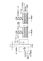
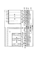
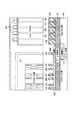
図73から図78は、そのレジストスリミング法によるロジック部のMOSトランジスタの製造工程における工程平面図および該平面図のX−X’、Y−Y’線に沿う工程断面図である。即ち、図73に示すように、素子領域100aおよび素子分離領域100bを有するシリコン基板100上に熱酸化法等によりゲート絶縁膜101を形成した後、前記ゲート絶縁膜101上にCVD(Chemical Vapor Deposition)法等により被加工材料膜、例えばゲート電極材料膜としてのポリシリコン膜102を堆積する。
【0007】
続いて、前記ポリシリコン膜102上にレジストを塗布・乾燥し、リソグラフィー(露光)を行って、第1のレジストパターン、例えばゲートレジストパターン103をリソグラフィー(露光)の解像限界寸法に形成する(ゲートレジストパターン形成工程)。この工程において、前記ゲートレジストパターン103は、前記素子領域100a上および前記素子分離領域100b上に形成する。ここで、前記素子領域100a上におけるパターン部をゲート電極パターン部103a、前記素子分離領域100b上におけるパターン部を配線パターン部103bと称する。
【0008】
次いで、図74に示すように、前記ゲートレジストパターン103をO2系ガスを用いた等方的ドライエッチング法等によりエッチング加工を施し、図中の破線で示すように、スリミング化させてリソグラフィーの解像限界以下のパターン寸法を有するゲートレジストパターン103’を形成する(ゲートレジストスリミング工程)。
【0009】
次いで、図75に示すように、前記ゲートレジストパターン103’をマスクにして、RIE(Reactive Ion Etching)法等により前記ポリシリコン膜102をエッチング加工して、前記素子領域100aに形成されたゲート電極パターン部104aおよび前記素子分離領域100b上に形成された配線パターン部104bを有するゲートパターン104を得る(ゲート電極加工工程)。
【0010】
次に、図76に示すように、前記ゲートレジストパターン103’をO2アッシング法等により前記ゲートパターン104の表面から剥離しする(レジスト剥離工程)。
【0011】
これにより、リソグラフィー解像限界寸法以下のパターン幅のゲートレジストパターン103’が形成可能となり、前記ゲートレジストパターン103’をマスクにゲート電極材料膜としての前記ポリシリコン膜102をエッチング加工することでリソグラフィーの解像限界以下のパターン幅をもつ微細なゲートパターン104が形成できる。
【0012】
上記の工程後、図示しないが、前記ゲート電極パターン部104aをマスクにして前記シリコン基板100の表面に不純物注入を行い、トランジスタのソース・ドレイン拡散層(図76の破線で示す)を形成した後、周知の層間絶縁膜形成、配線工程等を行うことにより、MOSトランジスが完成される。
【0013】
【発明が解決しようとする課題】
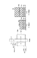
しかしながら、従来のレジストスリミング法では、ラインパターンに相当するゲート電極パターン部104aは、微細なパターン形成が可能であるが、逆に配線パターン部104bのスペース部がスリミングによって広がるためにスペース部のデザインルールは、スリミングを行なわないときよりも緩和しなければならない。即ち、図77に示すように、配線パターン部104bのスペース部の寸法(図中のゲートパターン突き当て間距離)tは、スリミングを施さない場合にはリソグラフィーの解像限界寸法t0まで詰めることができるが、スリミングを施した場合にはリソグラフィーの解像限界寸法t0に両側スリミング量t1を加えた寸法t0+2t1まで緩和しなければならない。
【0014】
この結果、従来のスリミング法では、トランジスタの微細ゲート電極パターン部の形成が可能であるためトランジスタの動作速度等の性能向上には効果があるものの、配線パターン部のスペース部のデザインルールが通常のリソグラフィー技術よりも緩和せざるを得ないため、チップ面積の縮小に効果がないという問題がある。
【0015】
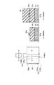
また、図78にDRAMメモリセル部のゲートパターンを示す。点線がスリミング前のレジストパターン、実線がスリミング後のレジストパターンである。メモリセル部では、集積度を向上させるため微細なパターンピッチが要求される。しかし、従来のレジストスリミング法をこのメモリセル部に施すと、スリミング後のスペースパターン寸法P1が、リソグラフィーのスペース解像限界まで詰めることができない。このことは、リソグラフィー段階でのスペースパターン寸法P2を緩和することを意味しており、その結果、メモリセル部のゲートパターンピッチが緩和され、比較的大規模なメモリセルが搭載されるシステムLSIでは、チップ面積が大きくなる可能性がある。
【0016】
ところで、ロジックとメモリーを混載する半導体デバイスのゲート層回路パターンをレベンソン型位相シフトマスクによる露光とロジックゲート部のレジストスリミングプロセスを組み合せる方法を用いて形成する場合では、ロジックゲート部にレベンソン型位相シフトマスクとトリムマスクを使用する2重露光によりレジストをパターニングした後、スリミングプロセスにより前記レジストパターンを細らせ、その後メモリーセル部および配線部の露光を行う必要がある。この方法の場合、露光回数は3回必要となる。つまり露光工程数の多いプロセスとなるといった課題があった。
【0017】
本発明の目的は、上記課題に鑑みなされたもので、微細パターンを形成することで高性能、かつ低コストで半導体装置を製造できる半導体装置の製造方法を提供することにある。
【0018】
また、本発明の他の目的は、DRAM Cell部においてより高解像度の回路パターンを得ることができる半導体装置の製造方法を提供することにある。
【0019】
また、本発明の他の目的は、露光工程数を削減して低コストで半導体装置を製造できる半導体装置の製造方法を提供することにある。
【0020】
【課題を解決するための手段】
上記課題を解決するために、この本発明の参考例に係る半導体装置の製造方法は、被加工膜上にマスク材料膜を堆積させ、該マスク材料膜上に第1の露光工程により第1のレジストパターンを形成する工程と、前記第1のレジストパターンをマスクに前記マスク材料膜を加工してマスクパターンを形成する工程と、前記第1のレジストパターンを剥離する工程と、前記マスクパターンを含む前記被加工膜上に、第2の露光工程により前記マスクパターンの選択領域を露出するための開口を有し、かつ非選択領域を被覆するような第2のレジストパターンを形成する工程と、前記第2のレジストパターンの開口内に露出された前記マスクパターン部分を細らせる工程と、前記第2のレジストパターンを剥離する工程と、前記マスクパターンをマスクに前記被加工膜をエッチング加工して、広い寸法幅のパターン部と細い寸法幅のパターン部とを有する被加工膜パターンを形成する工程とを具備することを特徴としている。
【0021】
また、この発明の参考例に係る半導体装置の製造方法は、前記被加工膜上にハードマスク材料膜を堆積させ、該ハードマスク材料膜上に第1の露光工程により第1のレジストパターンを形成する工程と、前記第1のレジストパターンをマスクに前記ハードマスク材料膜をエッチング加工してハードマスクパターンを形成する工程と、前記第1のレジストパターンを剥離する工程と、前記ハードマスクパターンを含む前記被加工膜上に、第2の露光工程により前記ハードマスクパターンの選択領域を露出するための開口を有し、かつ非選択領域を被覆するような第2のレジストパターンを形成する工程と、前記第2のレジストパターンの開口内に露出された前記ハードマスクパターン部をエッチング加工によって細らせる工程と、前記第2のレジストパターンを剥離する工程と、前記ハードマスクパターンをマスクに前記被加工膜をエッチングして広い寸法幅のパターン部と細い寸法幅のパターン部とを有する被加工膜パターンを形成する工程と、前記ハードマスクパターンを剥離せずに残存させた状態で、トランジスタのソース、ドレイン部コンタクトを、該ハードマスクパターンを用いた自己整合により形成する工程とを具備することを特徴としている。
【0022】
上記した発明の参考例によれば、露光の解像限界寸法に形成したレジストパターンをマスク材料膜、又はハードマスク材料膜に転写しマスクパターン、又はハードマスクパターンを形成した後、レジストパターンにより前記マスクパターン、又はハードマスクパターンの選択領域、例えばゲート電極パターン部を開口内に露出させ、かつ非選択領域、例えば配線パターン部を被覆し、前記露出された選択領域のパターンのみに選択的スリミングを施すため、チップ面積を増大させることなく、微細パターンの形成が可能で、例えばトランジスタの高性能化が図れる。
【0023】
また、この発明の参考例に係る半導体装置は、素子領域および素子分離領域上に、同時に形成された回路パターンを有する半導体装置において、前記回路パターンは、前記素子領域において細い寸法幅に形成されてなり、かつ前記素子分離領域において太い寸法幅に形成されてなることを特徴としている。
【0024】
上記した発明の参考例によれば、素子領域上の回路パターン部、例えばゲート電極パターンが露光の解像限界以下の寸法幅に形成されるため、トランジスタの動作速度等の性能が向上する。
【0025】
また、この発明に係る半導体装置の製造方法は、処理基板上に第1の材料を形成する工程と、レベンソン型位相シフトマスクを使用して第1の露光を行い前記第1の材料上の第1の領域に第1のレジストパターンを形成し、かつ第2の領域にレジストを被覆する工程と、前記第1のレジストパターンを細らせて第2のレジストパターンを形成する工程と、前記第2のレジストパターンをマスクとして前記第1の材料を加工する工程と、前記第2のレジストパターンを除去して前記第1の材料からなる第1のパターンを形成する工程と、前記第1の領域にレジストを覆い、かつ第2の露光を行って前記第2の領域に第3のレジストパターンを形成する工程と、前記第3のレジストパターンをマスクとして前記第1の材料を加工する工程と、前記第3のレジストパターンを除去して前記第1の材料からなる第2のパターンを形成する工程と、前記第1の材料からなる第2のパターンをマスクとして前記処理基板を加工する工程と、前記第1の材料を除去する工程とを具備することを特徴としている。
【0026】
また、この発明に係る半導体装置の製造方法は、処理基板上に第1の材料を形成する工程と、レベンソン型位相シフトマスクを使用して第1の露光を行い前記第1の材料上の第1の領域に第1のレジストパターンを形成し、かつ第2の領域にレジストを被覆する工程と、前記第1のレジストパターンをマスクとして前記第1の材料を加工する工程と、前記第1のレジストパターンを除去し前記第1の材料からなる第1のパターンを形成する工程と、前記第1の材料からなる第1のパターンを細らせて前記第1の材料からなる第2のパターンを形成する工程と、前記第1の領域をレジストで覆い、かつ第2の露光を行って前記第2の領域に第2のレジストパターンを形成する工程と、前記第2のレジストパターンをマスクとして前記第1の材料を加工する工程と、前記第2のレジストパターンを除去して前記第1の材料からなる第3のパターンを形成する工程と、前記第1の材料からなる第3のパターンをマスクとして前記処理基板を加工する工程と、前記第1の材料を除去する工程とを具備することを特徴としている。
【0027】
また、この発明に係る半導体装置の製造方法は、処理基板上に第1の材料を形成する工程と、レベンソン型位相シフトマスクを使用して第1の露光を行い、前記第1の材料上の第1の領域に第1のレジストパターンを形成し、かつ第2の領域にレジストを被覆する工程と、前記第1のレジストパターンをマスクとして前記第1の材料を加工する工程と、前記第1のレジストパターンを除去し、前記第1の材料からなる第1のパターンを形成する工程と、前記第1の領域をレジストで覆い、かつ第2の露光を行って前記第2の領域に第2のレジストパターンを形成する工程と、前記第2のレジストパターンをマスクとして前記第1の材料を加工する工程と、前記第2のレジストパターンを除去して前記第1の材料からなる第2のパターンを形成する工程と、前記第1の材料からなる第2のパターンをマスクとして処理基板を加工する工程と、前記第1の材料を除去する工程とを具備することを特徴としている。
【0028】
また、この発明に係る半導体装置の製造方法は、処理基板上に第1の材料を形成する工程と、レベンソン型位相シフトマスクを使用して第1の露光を行い、前記第1の材料上の第1の領域に第1のレジストパターンを形成し、かつ第2の領域にレジストを被覆する工程と、前記第1のレジストパターンを細らせて第2のレジストパターンを形成する工程と、前記第2のレジストパターンをマスクとして前記第1の材料を加工する工程と、前記第2のレジストパターンを除去して前記第1の材料からなる第1のパターンを形成する工程と、前記第1の材料からなる第1のパターンを細らせて前記第1の材料からなる第2のパターンを形成する工程と、前記第1の領域にレジストを覆い、かつ第2の露光を行って前記第2の領域に第3のレジストパターンを形成する工程と、前記第3のレジストパターンをマスクとして前記第1の材料を加工する工程と、前記第3のレジストパターンを除去して前記第1の材料からなる第3のパターンを形成する工程と、前記第1の材料からなる第3のパターンをマスクとして処理基板を加工する工程と、前記第1の材料を除去する工程とを具備することを特徴としている。
【0029】
上記した発明によれば、前記処理基板上に形成した第1の材料(マスク材料膜)、例えばハードマスク材料膜を用いて、2回のリソグラフィー工程(第1、第2の露光)を行って所望の回路パターンを形成するので、従来の半導体装置の製造方法と比較して露光工程数を低減することができ、製造コストを削減することができる。
【0030】
【発明の実施の形態】
以下、図面を参照しながら本発明の実施の形態について説明する。
【0031】
参考例1
本発明の参考例1に係る半導体装置の製造方法について説明する。
【0032】
この参考例1は、ロジックとメモリを混載したシステムLSIに適用した例である。図1から図9は、レジストスリミング法によるロジック部のMOSトランジスタの各工程における工程平面図および該平面図のX−X’、Y−Y’線に沿う工程断面図である。
【0033】
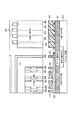
即ち、図1に示すように、素子領域1aおよび素子分離領域1bを有するシリコン基板1上の熱酸化法等により、ゲート絶縁膜2を膜厚1〜3nmに形成した後、低圧CVD法等により、被加工材料膜(被加工膜)、例えばゲート電極材料膜としてポリシリコン膜3を膜厚150〜200nmに形成する。続いて、前記ポリシリコン膜3上に、スパッタ法等によりマスク材料膜、例えばハードマスク材料膜(第1の材料)としての、例えばSiON膜4を膜厚50から100nmに形成する。このハードマスク材料膜4としては、SiONの他に、SiO2、Si3N4や下地からの光学的反射防止膜となるAl2O3、SiC、カーボン膜を単独、若しくは組合わせて用いてもよい。
【0034】
次いで、前記SiON膜4上にフォトレジストを回転塗布し、かつ乾燥させた後、第1のリソグラフィー(露光)工程(第1の露光工程)により、前記素子領域1aおよび前記素子分離領域1b上の前記SiON膜4上に、レジストパターン(第1のレジストパターン)、例えばゲートレジストパターン5をリソグラフィーの解像限界寸法に形成する(ゲートレジストパターン形成工程)。このとき、レジスト塗布前に塗布型反射防止膜を塗布しても良い。
【0035】
ここで、前記素子領域1a上のゲートレジストパターン部をゲート電極パターン部5a、前記素子分離領域1b上のゲートレジストパターン部を配線パターン部5bと称する。
【0036】
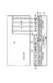
次いで、図2に示すように、前記ゲートレジストパターン5をマスクに前記SiON膜4をRIE法等によりドライエッチング加工して、ゲート電極パターン部6aおよび配線パターン部6bをもつハードマスクパターン6を形成する(ハードマスク加工工程)。前記塗布型反射防止膜が形成されている時は、このハードマスク加工工程の前に前記反射防止膜加工工程が入る。このハードマスク加工工程において、エッチングガスとしては、CHF3等のフロロカーボン系のガスを用いる。
【0037】
次いで、図3に示すように、前記ゲートレジストパターン5をO2アッシング法等により剥離する(レジスト剥離工程)。この工程において、レジスト剥離は、過酸化水素水と硫酸の混合液を単独、若しくは組合わせた剥離液を用いた湿式エッチング法を用いてもよい。
【0038】
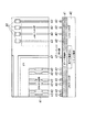
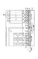
次いで、図4に示すように、前記ハードマスクパターン6を含む前記シリコン基板1上に、フォトレジストを回転塗布し、かつ乾燥させた後、第2のリソグラフィー(露光)工程により、所定パターンを有する耐エッチング材としての第2のレジストパターン7を形成する(スリミングパターン露呈工程)。
【0039】
この工程では、前記第2のレジストパターン7は、スリミングによって細らせたい部分(例えば、ロジック部のゲート電極パターン部等)を開口7aさせ、かつスリミングを施したくない部分(例えば、微細スペースパターン部が形成される素子分離領域1b上の配線パターン部、比較的密集度の高いメモリセルパターン部等)を覆うようなパターンに形成される。そして前記開口7aは、素子領域1aとの合せずれ余裕を見込んで、素子領域1aの面積よりやや大きく、例えば数10nm程度大きく形成することが望ましい。
【0040】
また、この工程では、フォトレジストとしては、前記素子分離領域1bの形成において用いるフォトレジストと反対のトーンをもつレジスト、例えば素子分離領域1bの形成においてポジ型レジストを使用した場合には、ネガ型レジストを、逆にネガ型レジストの場合には、ポジ型レジストを使用すると素子分離領域1bの形成工程で用いた素子分離領域形成の露光マスクが利用でき経済的であるため、好ましい。
【0041】
また、この第2のリソグラフィー工程は、段差パターン(ハードマスクパターン)上でのレジスト形成となるので、平坦化材料を用いた多層レジストプロセスを用いてもよい。
【0042】
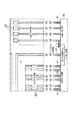
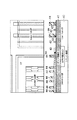
次いで、図5に示すように、前記第2のレジストパターン7をマスクにして、前記第2のレジストパターン7の開口7a内に露呈された前記ゲート電極パターン6aに対してCDE(Chemical Dry Etching)法、やRIE法等によるドライエッチング法、若しくは湿式エッチング法によるエッチングを施し、図中の破線で示すように、前記開口7a内の前記ゲート電極パターン部6aのみを選択的にスリミング化させてリソグラフィーの解像限界以下のパターン寸法に形成する(ハードマスク電極加工工程)。
【0043】
この工程において、前記ゲート電極パターン部6aのエッチングとしてドライエッチングを行なう場合、エッチングガスとしては、例えば、CHF3等のフロロカーボン系のガスを用いる。湿式エッチングを行なう場合は、hot H3PO4を用いる。
【0044】
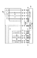
次いで、図6に示すように、前記第2のレジストパターン7をO2アッシング法等により剥離する(レジスト剥離工程)。この工程において、レジスト剥離は、過酸化水素水と硫酸の混合液を単独、若しくは組合わせた剥離液を用いた湿式エッチング法を用いてもよい。
【0045】
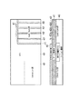
次いで、図7に示すように、前記ハードマスクパターン6をマスクにRIE法等のドライエッチングにより前記ポリシリコン膜3をエッチング加工して、ゲート電極パターン部8aと配線パターン部8bをもつゲートパターン8を得る(ゲート電極加工工程)。続いて、前記ゲート絶縁膜2をエッチングする。この工程では、前記ポリシリコン膜3のエッチングガスとしては、Cl2、HBr等のハロゲン系ガスを用いる。
【0046】
次に、図8に示すように、前記ハードマスクパターン6を湿式エッチング法等によりエッチング除去する(ハードマスク剥離工程)。この工程では、エッチング液としては、hot H3PO4を用いる。
【0047】
これにより、図9に示すように、微細ライン寸法が要求される個所(ロジック部のトランジスタのゲート電極パターン部)、例えばゲート電極パターン部8aは、スリミングにより、リソグラフィー解像限界寸法以下の微細なパターンに形成され、微細スペースが要求される個所(素子分離上のゲートパターン間スペースやメモリセル部)、例えば配線パターン部8bは、スリミングより広がらず、リソグラフィーの解像限界の微細スペースに、各々、形成される。
【0048】
上記の工程後、図示しないが、前記ゲート電極パターン部8aをマスクに前記シリコン基板1の表面に不純物注入して、トランジスタのソース・ドレイン拡散層(図8の破線で示す)を形成した後、周知の層間絶縁膜形成工程、配線工程等を行うことにより、MOSトランジスタが完成される。
【0049】
この参考例1によれば、微細ライン寸法が要求される個所(ロジック部のトランジスタのゲート電極パターン部)にのみを、選択的スリミングを行うことで、スリミングによる微細ゲート電極パターン8a(ラインパターン)と、スリミングを施さないことによる微細配線パターン8b(スペースパターン)を形成することが可能で、トランジスタの動作速度等の性能向上とチップのシュリンクを同時に実現することができる。
【0050】
次に、実際のデザインルールの各項目に照らし合わせて、本参考例1の方法と従来の方法とを比較検証する。
【0051】
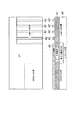
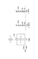
図10は、実際のゲート(GC)層/素子領域(AA)層のパターンレイアウトとデザインルールの項目を示す。なお、図10は、従来の方法と本参考例1による転写後のパターン平面形状を示している。
【0052】
図中、記号のA0はトランジスタのゲート長で、このゲート長のデザインルールは、本参考例1においても、従来の方法と同等のルールが設定でき、スリミングによるゲート長の微細化によって高性能のトランジスタが実現できる。A1は素子分離領域上の配線パターン幅で、この個所については、本参考例1に比べて従来の方法ではスリミングが施されるため、微細なパターンになる。しかしながらA1に関する部位のチップサイズに与えるインパクトは、ゲートコンタクトフリンジが決定する場合が多く、このゲートコンタクトフリンジはゲートーコンタクト合わせ余裕によって決まるため、ある程度のゲートコンタクトフリンジがA1とは独立に必要である。即ち、A1の設計値が微細になってもチップサイズに与えるインパクトは小さい。
【0053】
また、ゲート間のスペースB0Aおよび素子分離領域を横切るゲートのスペースB0Bのルールは、本参考例1でも従来の方法でも同じ値となる。ゲート配線パターンのスペースB1は、本参考例1ではリソグラフィーの解像限界寸法まで小さくすることができ、チップサイズ縮小に対するインパクトが大きい。Cはトランジスタのエンドキャップと呼ばれるもので、この個所はラインショートニングと合わせずれによりゲート端がAA上に乗りあがるのを防ぐためにある程度の領域(面積)を確保しておく必要がある。即ち、従来の方法では素子分離領域上のスリミングを見込んでスリミング前は点線の領域でパターニングしておく必要があり、この領域は本参考例1のパターニングされる領域よりも大きくなる。そのため、従来の方法では、リソグラフィー段階における素子分離領域上のスペース(図中のGap)をレジスト形成時でのショートを避けるため、ある程度大きく設定する必要があり、チップ縮小に不利となる。このことは、ゲート配線パターンとAAとの間隔Eについても同様である(EのルールはGC−AA合わせ余裕で決定されるため)。ゲートとAAの距離Dのルールは、従来の方法でも本参考例1でも同じ値となる。ゲートの最小島領域Fは従来の方法が微細なパターンが形成可能であるが、島パターンが小さくなってもスペースが小さくできなければチップサイズ縮小にインパクトを与えない。
【0054】
以上のように、A0,B0A,B0B,D,Fのルールについては、従来の方法、本参考例1とも差が無く、A1、B1、C,Eについては、本参考例1の方が従来法よりもチップ面積縮小に対して有利であり、総合的に本参考例1がチップ面積縮小に対して優れていることが明らかである。
【0055】
また、本参考例1によれば、素子領域上のパターンに対しては、スリミングを施し、素子分離領域上のパターンに対しては、スリミングを施さないので、前記第2の露光工程で転写される前記第2のレジストパターン7は、前記素子領域1aの反転パターンとなる。その場合、前記素子領域1aと前記第2のレジストパターン7との合わせずれ余裕を見込み、前記第2の露光工程で転写される第2のレジストパターン7の開口7aは、前記素子領域1aの面積よりもやや大きく形成することもできる。更にこの場合、前記第2の露光工程に素子分離領域形成において用いたレジストとトーン(ポジ型、若しくはネガ型)と反対のトーンのレジストを用いると、前記第2の露光工程に用いるマスクは素子分離領域形成に用いるマスクと同一のものが使用でき経済的である。
【0056】
また、本参考例1においては、メモリセル部は、スリミングが施されないように、第2のレジストパターンによりマスクしているので、第1の露光工程によるリソグラフィーの解像限界寸法を維持する。そのため、比較的大規模なメモリセルが搭載されるシステムLSIにおいても、従来のように、チップ面積を増加させることはない。
【0057】
また、本参考例1の半導体装置によれば、ゲート長がスリミングによりリソグラフィーの解像限界以下の寸法にできるため、トランジスタの動作速度等の高性能化が図れる。
【0058】
参考例2
次に、本発明の参考例2に係る半導体装置の製造方法について図11から図15を用いて説明する。本参考例2も、参考例1と同様に、ロジックとメモリを混載したシステムLSIに適用して例であるが、本参考例2では、ゲート電極加工後にハードマスクを剥離せずにそのまま残存させ、該ハードマスクをソース・ドレイン拡散層とのセルフアラインコンタクトに利用するようにものである。
【0059】
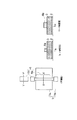
図11は、レジストスリミング法によるゲート電極加工工程を示す工程平面図および該平面図のX−X’線に沿う工程断面図、図12から図15は、セルフアラインコンタクト形成までの各製造工程の工程断面図である。即ち、本参考例2では、まず、上記参考例1と同様に、ゲートレジストパターン形成工程、ハードマスク加工工程、レジスト剥離工程、反転リソグラフィー工程、ハードマスクスリミング工程、ゲート電極加工工程およびレジスト剥離工程を、順次、経て、図11に示すような、シリコン基板1の素子領域1a上に、スリミングによってリソグラフィー解像限界寸法以下に形成された微細なゲート電極パターン部(ラインパターン)8aを有し、かつ素子分離領域1b上に、スリミングが施されなかった微細配線パターン部(スペースパターン部)8bを有するゲートパターン8を得る(ゲート電極加工工程)。
【0060】
次いで、図12に示すように、前記シリコン基板1上に最終的にゲート側壁膜となる、例えばSi3N4膜をCVD法等により膜厚25〜100nmに堆積した後、RIE法等によりエッチングして前記ハードマスクパターン6aおよび前記ゲート電極パターン8a側壁にゲート側壁膜20を形成する(側壁絶縁膜形成工程)。この工程では、エッチングガスとしては、Cl2,HBr等のハロゲン系のガスを用いる。
【0061】
次いで、図13に示すように、前記ゲート電極パターン8aを含む前記シリコン基板1上にCVD法等により酸化膜等の層間絶縁膜21を膜厚0,5μm〜2.0μmに堆積(層間絶縁膜形成工程)後、前記層間絶縁膜21上面をCMP(Chemical Mechanical Polishing)法により平坦化する(層間絶縁膜平坦化工程)。続いて、前記層間絶縁膜21上にコンタクト形成用のレジストパターン22を形成する(コンタクトレジスト形成工程)。
【0062】
次いで、図14に示すように、前記レジストパターン22をマスクにRIE法等で前記層間絶縁膜21をエッチング除去して前記シリコン基板1表面のソース・ドレイン拡散層23に達するコンタクト孔24を形成する(層間絶縁膜エッチング工程)。この工程では、エッチングガスとしては、CxFx等のフロロカーボン系のガスを用い、層間絶縁膜21とゲート側壁膜20とのエッチング選択比によってコンタクト孔24を形成する。
【0063】
次いで、図15に示すように、前記レジストパターンを酸素アッシング法等により剥離(レジスト剥離工程)した後、ポリシリコン等の電極材料をCVD法等により前記コンタクト孔24を埋め込むように堆積させ、例えば不要な部分の電極材料を除去して前記コンタクト孔24内に埋め込みコンタクト25を形成する(コンタクト形成工程)。
【0064】
この参考例2によれば、上記参考例1と同様なスリミングによる微細ラインパターンと、スリミングを行なわないことによる微細スペースパターンを形成することが可能である。また、ゲート電極パターンがリソグラフィーの解像限界以下の寸法に形成されているので、トランジスタの動作速度等の性能向上が図れる。しかも、トランジスタの性能向上とチップのシュリンクを同時に実現することができる効果の他に、次のような効果が得られる。
【0065】
即ち、前記ハードマスクパターン6aを前記ゲート電極パターン8a上に残しておき、前記層間絶縁膜(SiO2)21と前記ハードマスクパタン6aとのエッチング選択比によって、コンタクト孔24の形成を行うことにより、前記ゲート電極パターン部8aを保護して、かつ前記コンタクト孔24を自己整合的に形成できるので、製造工程を簡略化できる。
【0066】
参考例3
次に、本発明の参考例3に係る半導体装置の製造方法について図16から図21を用いて説明する。本参考例3も、参考例1と同様に、ロジックとメモリを混載したシステムLSIに適用した例であるが、本参考例3では、ハードマスクに代えて多層レジストプロセスを用いたことを特徴としている。
【0067】
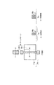
図16から図21は、その製造工程を示す工程平面図および該平面図のX−X’、Y−Y’線に沿う工程断面図である。即ち、参考例3では、まず、図16に示すように、素子領域31aおよび素子分離領域31bを有するシリコン基板31の表面にゲート絶縁膜32、被加工膜、例えばゲート電極材料膜としてのポリシリコン膜33を、順次、堆積した後、前記ポリシリコン膜33上に多層レジスト膜34を形成する。
【0068】
そして、前記多層レジスト膜34は、前記ポリシリコン膜33上に形成されるカーボン、若しくはノボラック系レジスト等の有機膜からなる下層膜341と、前記下層膜341上に形成されるSOG(Spin on Glass)、SiO2等の中間膜342と、前記中間膜342上に形成されるフォトレジスト膜343とから構成され、前記下層膜341および前記中間膜342は、光学的反射防止膜としての機能を有する。また、前記下層膜341、又は前記中間膜342は、被加工膜のエッチング加工のためのマスク材として機能する。また、前記下層膜341、前記中間膜342および前記フォトレジスト膜343は、例えば回転塗布後、乾燥させることにより形成され、前記下層膜341は、膜厚0.5μm程度に形成され、前記中間膜342は、膜厚10nm程度に形成され、前記フォトレジスト膜343は、膜厚0.2μm程度に形成される。
【0069】
次いで、第1のリソグラフィー(露光)工程により、前記フォトレジスト膜343をパターニングして前記素子領域31aおよび前記素子分離領域31b上に、ゲートレジストパターン35をリソグラフィーの解像限界寸法に形成する(ゲートレジストパターン形成工程)。ここで、前記素子領域31a上のゲートレジストパターン部をゲート電極パターン部35a、前記素子分離領域31b上のゲートレジストパターン部を配線パターン部35bと称する。
【0070】
次いで、図17に示すように、前記ゲートレジストパターン35をマスクに前記反射防止膜、即ち前記中間膜342および前記下層膜341を、順次、CDE法等のドライエッチングによりパターニングして、中間膜パターン36および下層膜パターン37を形成する(反射防止膜加工工程)。この工程では、前記中間膜342のエッチングガスとしては、CHF3/O2等のフロロカーボン系のガスを用い、前記下層膜341のエッチングガスとしては、例えばノボラック系レジストの場合には、N2/O2の混合ガスを用いる。また、前記中間膜パターン36および前記ゲート下層膜パターン37は、いずれも、ゲート電極パターン部36a、37aおよび配線パターン部36b、37bを有する。なお、前記下層膜パターン37のパターニングの際に、前記フォトレジスト膜パターン35および前記中間膜パターン36は、膜減りして最終的には消滅してなくなる。従って、前記下層膜パターン37が、後述するポリシリコン膜のエッチング加工の際のマスクパターンとして機能することになる。
【0071】
次いで、図18に示すように、上記参考例1と同様に、前記下層膜パターン37を含む前記シリコン基板31上に、フォトレジストを回転塗布し、かつ乾燥させた後、第2のリソグラフィー(露光)工程により、前記下層膜パターン37の前記ゲート電極パターン部37aを開口38a内に露出し、かつ前記配線パターン部37bを被覆するような所定パターンを有する耐エッチング材としての第2のレジストパターン38を形成する(スリミングパターン露呈工程)。
【0072】
この工程では、前記第2のレジストパターン38は、後述の前記下層膜パターン37のエッチングによるスリミング工程において、耐エッチング性を有する選択比のものを用いる。また、前記開口38aは、素子領域との合せずれ余裕を見込んで、素子領域面積よりやや大きく、例えば数10nm程度大きく形成することが望ましい。また、フォトレジストとしては、前記素子分離領域の形成において用いるフォトレジストと反対のトーンをもつレジスト、例えば素子分離領域の形成においてポジ型レジストを使用した場合には、ネガ型レジストを、逆にネガ型レジストの場合には、ポジ型レジストを使用すると素子分離領域の形成工程で用いた素子分離領域形成の露光マスクが利用でき経済的であるため、好ましい。
【0073】
また、この第2のリソグラフィー工程は、段差パターン(ハードマスクパターン)上でのレジスト形成となるので、平坦化材料(平坦化膜)を用いた多層レジストプロセスを用いてもよい。
【0074】
次いで、図19に示すように、前記第2のレジストパターン38をマスクにして、前記第2のレジストパターン38の開口38a内に露呈された前記下層膜パターン37のゲート電極パターン部37aに対してCDE法等による等方的エッチングを施し、図中の破線で示すように、前記開口38a内の前記ゲート電極パターン部37aのみを選択的にスリミング化させてリソグラフィーの解像限界以下のパターン寸法に形成する(下層膜スリミング加工工程)。この工程において、前記下層膜パターン部37aのエッチングガスとしては、例えば、N2/O2の混合ガスを用いる。
【0075】
次いで、図20に示すように、前記下層膜パターン37をマスクにRIE法等のドライエッチングにより前記ポリシリコン膜33をエッチング加工して、ゲート電極パターン部39aと配線パターン部39bをもつゲートパターン39を得る(ゲート電極加工工程)。続いて、前記ゲート絶縁膜32をエッチングする。この工程において、前記ポリシリコン膜33のエッチングガスとしては、Cl2、HBr等のハロゲン系ガスを用いる。
【0076】
次に、図21に示すように、前記下層膜パターン37をO2アッシング法等により剥離する(下層膜剥離工程)。
【0077】
これにより、微細ライン寸法が要求される個所(ロジック部のトランジスタのゲート電極パターン部)、例えばゲート電極パターン部39aは、スリミングにより、リソグラフィー解像限界寸法以下の微細なパターンに形成され、微細スペースが要求される個所(素子分離上のゲートパターン間スペースやメモリセル部)、例えば配線パターン部39bは、スリミングされず、リソグラフィーの解像限界寸法をもつ微細スペースに、各々、形成される。
【0078】
上記の工程後、図示しないが、前記ゲート電極パターン部39aをマスクに前記シリコン基板31の表面に不純物注入して、トランジスタのソース・ドレイン拡散層(図21中の破線)を形成した後、周知の層間絶縁膜形成工程、配線工程等を行うことにより、MOSトランジスタが完成される。
【0079】
この参考例3によれば、上記参考例による効果の他に、第1のレジストパターン35となるフォトレジスト膜343は、膜厚10nm程度の薄い中間膜342をパターニングするに必要な膜厚でよく、例えば従来の場合、0.4μmおよび参考例1の場合、0.3μmに比べて薄くできるため、解像度の向上により、パターンの加工精度が向上する。また、このためトランジスタの性能をより向上できる。
【0080】
参考例4
次に、本発明の参考例4に係る半導体装置の製造方法について図22から図27を用いて説明する。図において、前記参考例3と同一の機能および構成を有する構成要素部分には、同一符号を付して詳しい説明を省略する。
【0081】
本参考例4と上記参考例3とが異なる点は、スリミング工程で、上記参考例3では、下層膜パターンに対してスリミングを行ったが、本参考例4では、中間膜パターンに対してスリミングを行う点で異なるものである。
【0082】
即ち、まず、図22に示すように、素子領域31aおよび素子分離領域31bを有するシリコン基板31の表面にゲート絶縁膜32、ポリシリコン膜33を堆積し、続いて、多層レジスト膜34としての下層膜341、中間膜342およびフォトレジスト膜343を順次、堆積した後、第1のリソグラフィー(露光)工程により、前記フォトレジスト膜343をパターニングして前記素子領域31a上にゲート電極パターン部35aを、前記素子分離領域31b上に配線パターン部35bを有するゲートレジストパターン35をリソグラフィーの解像限界寸法に形成する(ゲートレジストパターン形成工程)。
【0083】
次いで、図23に示すように、前記ゲートレジストパターン35をマスクに前記中間膜342をRIE法等によりドライエッチングして、前記素子領域31a上にゲート電極パターン部36aを有し、かつ素子分離領域31b上に配線パターン部36bを有する中間膜パターン36を形成する(反射防止膜加工工程)。この工程では、前記中間膜342のエッチングガスとしては、CHF3/O2の混合ガス等のフロロカーボン系のガスを用いる。
【0084】
次いで、前記中間膜パターン36上の前記フォトレジストパターン35をO2アッシングにより剥離(レジスト膜剥離工程)した後、図24に示すように、上記参考例3と同様に、第2のリソグラフィー(露光)工程により、前記中間膜パターン36の前記ゲート電極パターン部36aを開口内に露出し、かつ前記配線パターン部36bを被覆するような所定パターンを有する耐エッチング材としての第2のレジストパターン38を形成する(スリミングパターン露呈工程)。ここで、前記第2のレジストパターン38は、後述の前記中間膜パターン36のエッチングによるスリミング工程において、耐エッチング性を有する選択比のものを用いる。
【0085】
また、前記開口38aは、素子領域との合せずれ余裕を見込んで、素子領域面積よりやや大きく、例えば数10nm程度大きく形成することが望ましい。また、フォトレジストとしては、前記素子分離領域の形成において用いるフォトレジストと反対のトーンをもつレジスト、例えば素子分離領域の形成においてポジ型レジストを使用した場合には、ネガ型レジストを、逆にネガ型レジストの場合には、ポジ型レジストを使用すると素子分離領域の形成工程で用いた素子分離領域形成の露光マスクが利用でき経済的であるため、好ましい。
【0086】
また、この第2のリソグラフィー工程は、段差パターン(ハードマスクパターン)上でのレジスト形成となるので、平坦化材料を用いた多層レジストプロセスを用いてもよい。
【0087】
次いで、図25に示すように、前記第2のレジストパターン38をマスクにして、前記第2のレジストパターン38の開口38a内に露呈された前記中間膜パターン36aに対してCDE法等による等方的エッチングを施し、図中の破線で示すように、前記開口38a内の前記中間膜パターン部36aのみを選択的にスリミング化させてリソグラフィーの解像限界以下のパターン寸法に形成する(中間膜スリミング加工工程)。この工程において、前記中間膜パターン部36aのエッチングガスとしては、例えば、CHF3/O2の混合ガス等のフロロカーボン系のガスを用いる。
【0088】
次いで、図26に示すように、前記中間膜パターン36をマスクに用いてRIE法等のドライエッチングにより前記下層膜341をエッチング加工し、更に前記ポリシリコン膜33をエッチング加工して、ゲート電極パターン部39aと配線パターン部39bをもつゲートパターン39を得る(ゲート電極加工工程)。続いて、前記ゲート絶縁膜32をエッチングする。前記中間膜のエッチングガスとしては、N2/O2の混合ガスを用い、前記ポリシリコン膜33のエッチングガスとしては、Cl2、HBr等のハロゲン系ガスを用いる。前記中間膜パターン36は、前記ポリシリコン膜33のエッチングの際、膜減りして最終的に消滅してなくなる。
【0089】
次に、図27に示すように、前記下層膜パターン37をO2アッシング法等により剥離する(下層膜剥離工程)。これにより、微細ライン寸法が要求される個所(ロジック部のトランジスタのゲート電極パターン部)、例えばゲート電極パターン部39aは、スリミングにより、リソグラフィー解像限界寸法以下の微細なパターンに形成され、微細スペースが要求される個所(素子分離上のゲートパターン間スペースやメモリセル部)、例えば配線パターン部39bは、スリミングされず、リソグラフィーの解像限界寸法の微細スペースに、各々、形成される。
【0090】
上記の工程後、図示しないが、前記ゲート電極パターン部39aをマスクに前記シリコン基板31の表面に不純物注入して、トランジスタのソース・ドレイン拡散層(図27中の破線)を形成した後、周知の層間絶縁膜形成工程、配線工程等を行うことにより、MOSトランジスタが完成される。
【0091】
この参考例4によれば、上記参考例3と同様に、第1のレジストが薄くでき、解像度が向上するため、パターンの加工精度が向上し、トランジスタの性能をより向上できる。
【0092】
実施の形態1
本発明の実施の形態1に係る半導体装置の製造方法を、図28〜図36を用いて以下に説明する。図28〜図36は、半導体装置のゲート層パターン形成のフロー断面図および平面図を示す。
【0093】
本実施の形態1では、レベンソン型位相シフトマスクを使用した第1の露光によりLogic Gate部のゲートパターンを形成し、トリムマスクを使用した第2の露光によりDRAM Cell部および配線部となる素子分離部のパターンを形成するものである。ゲートパターンおよび配線パターンを形成する工程では、レジストとゲート電極材との間にハードマスク材料膜となる絶縁膜を形成する。そして、Logic Gate部のレジストパターンに対してスリミングを行うものである。
【0094】
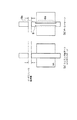
先ず、図28に示すように、熱酸化法等によりシリコン基板(処理基板)40上に素子分離部を形成する。これにより、Logic Gate部(第1の領域、例えばトランジスタのゲート領域)、DRAM Cell部(第2の領域、例えばメモリセル部)およびSiO2からなる素子分離部(第2の領域)が形成される。
【0095】
次に、低圧CVD法等により、被加工材料膜であるゲート電極材料膜41として、膜厚150〜200nmのポリシリコン膜を形成する。
【0096】
次に、ポリシリコン膜からなるゲート電極材膜41上に、スパッタ法等によりハードマスク材料膜(第1の材料)42としての膜厚50〜100nmのSiON膜を形成する。このハードマスク材料膜42としては、SiONの他に、SiO2、Si3N4や下地からの光学的反射防止膜となるAl2O3、SiC、カーボン膜等を単独、若しくは組合せて用いてもよい。
【0097】
次に、ハードマスク材料膜42上にフォトレジスト(レジスト)を回転塗布し、かつ乾燥させる。
【0098】
次に、レベンソン型位相シフトマスクを使用して、第1のリソグラフィー工程(第1の露光)によりLogic Gate部にレジストパターン(第1のレジストパターン)を形成する。これは、リソグラフィーの解像限界寸法で形成する(ゲートレジストパターン形成工程)。このとき、レジスト塗布前に塗布型反射防止膜を塗布しても良い。
【0099】
次に、図29に示すように、Logic Gate部のレジストパターンに対してドライエッチング等でスリミングを行い、より微細なレジストパターン(第2のレジストパターン)を形成する。このレジストパターンのフォトレジストとしては、DRAM Cell部および素子分離部に形成するフォトレジストと反対のトーンをもつフォトレジスト、例えば、DRAM Cell部および素子分離部に形成するフォトレジストとしてポジ型レジストを用いた場合には、Logic Gate部にはネガ型レジストを用い、逆に、DRAM Cell部および素子分離部に形成するフォトレジストとしてネガ型レジストを使用した場合には、Logic Gate部にはポジ型レジストを使用する。これにより、DRAM Cell部および素子分離部のフォトレジストの形成工程で用いた露光マスクが利用でき経済的であるため好ましい。
【0100】
次に、図30に示すように、レジストパターンをマスク材として、RIE(Reactive Ion Etching)法等によりLogic Gate部のハードマスク材料膜42をドライエッチング加工し、ハードマスクパターン(第1のパターン)を形成する(ハードマスク材料膜の加工工程)。エッチングガスとしては、CHF3等のフロロカーボン系のガスを用いる。
【0101】
その後、図31に示すように、O2アッシング法等によりフォトレジスト43の剥離を行う。これにより、ハードマスクパターン(第1のパターン)が露出する。(レジスト剥離工程)。フォトレジスト43の剥離工程では、過酸化水素水と硫酸の混合液を単独、若しくは組合せた剥離液を用いた湿式エッチング法を用いてもよい。
【0102】
次に、図32に示すように、トリムマスクを使用して、Logic Gate部のハードマスクパターンをフォトレジスト(レジスト)44で覆い、かつ、第2のリソグラフィー工程(第2の露光)によりDRAM Cell部および素子分離部にフォトレジストのパターン(第3のレジストパターン)44を形成する。
【0103】
次に、図33に示すように、Logic Gate部のレジスト44をマスク材として、DRAM Cell部および素子分離部のハードマスク材料膜42をドライエッチング加工し、ハードマスクパターンを形成する(ハードマスク材料膜の加工工程)。エッチングガスとしては、CHF3等のフロロカーボン系のガスを用いる。
【0104】
その後、図34に示すように、アッシング法等によりレジスト44の剥離を行う。(レジスト剥離工程)。レジスト44の剥離工程では、過酸化水素水と硫酸の混合液を単独、若しくは組合せた剥離液を用いた湿式エッチング法を用いてもよい。
【0105】
次に、図35に示すように、RIE法等によりハードマスク材料膜42のパターンをマスク材としてゲート電極材膜41をエッチングする。これにより、ゲート電極パターンおよび配線パターンをもつハードマスクパターン(第2のパターン)を形成する。エッチングガスとしては、CHF3等のフロロカーボン系のガスを用いる。
【0106】
その後、図36に示すように、湿式エッチング法等によりハードマスクパターンであるハードマスク材料膜42を剥離する(ハードマスク剥離工程)。エッチング液としては、hot H3PO4を用いる。これにより、半導体装置のゲート電極パターンおよび配線パターンが形成される。
【0107】
以上説明したように、実施の形態1に係る半導体装置の製造方法によれば、2回のリソグラフィー工程(第1、第2の露光)により、所望の回路パターンを形成することができるので、従来の半導体装置の製造方法と比較して露光工程数を低減することができ、製造コストを削減することができる。
【0108】
これに対して、従来の半導体装置の製造方法では、すなわちハードマスク材料膜42を介さないプロセスを用いて半導体装置の回路パターンを形成しようとする場合、レベンソン型位相シフトマスクを使用したLogic Gate部に関する第1の露光と、トリムマスクを使用したLogic Gate部および素子分離部に関する第2の露光と、さらにスリミングプロセスを経た後のDRAM Cell部に関する第3の露光が必要となる。
【0109】
なお、実施の形態1に係る半導体装置の製造方法において、ハードマスク材料膜としては、SiON、Si3N4、SiO2、Al2O3、SiC、カーボン膜のうちのいずれか1つ、あるいはそれらの組み合わせを用いてもよい。
【0110】
また、レベンソン型位相シフトマスクを使用した第1の露光、およびトリムマスクを使用した第2の露光によるレジストパターンの形成には、ハードマスク材料膜上に直接形成する場合、および反射防止膜上に形成する場合、また多層レジストマスクプロセスによって形成する場合のいずれでもよい。
【0111】
また、トリムマスクとしては、クロムマスク、あるいは、ハーフトーンマスクであり、ハーフトーンマスクを使用した方が半導体装置のDRAM Cell部において、より高解像度の回路パターンを得ることができる。
【0112】
実施の形態2
本発明の実施の形態2に係る半導体装置の製造方法を、図37〜図45を用いて以下に説明する。図37〜図45は、半導体装置のゲート層パターン形成のフロー断面図および平面図を示す。
【0113】
本実施の形態2では、レベンソン型位相シフトマスクを使用した第1の露光によりLogic Gate部のゲートパターンを形成し、トリムマスクを使用した第2の露光によりDRAM Cell部および配線部となる素子分離部のパターンを形成するものである。ゲートパターンおよび配線パターンを形成する工程では、レジストとゲート電極材との間にハードマスク材料膜となる絶縁膜を形成する。そして、Logic Gate部のハードマスク材料膜のパターンに対してスリミングを行うものである。
【0114】
先ず、図37に示すように、熱酸化法等によりシリコン基板(処理基板)40上に素子分離部を形成する。これにより、Logic Gate部(第1の領域、例えばトランジスタのゲート領域)、DRAM Cell部(第2の領域、例えばメモリセル部)およびSiO2からなる素子分離部(第2の領域)が形成される。
【0115】
次に、低圧CVD法等により、被加工材料膜であるゲート電極材料膜41として、膜厚150〜200nmのポリシリコン膜を形成する。
【0116】
次に、ポリシリコン膜からなるゲート電極材膜41上に、スパッタ法等によりハードマスク材料膜(第1の材料)42としての膜厚50〜100nmのSiON膜を形成する。このハードマスク材料膜42としては、SiONの他に、SiO2、Si3N4や下地からの光学的反射防止膜となるAl2O3、SiC、カーボン膜等を、単独若しくは組合せて用いてもよい。
【0117】
次に、ハードマスク材料膜42上にフォトレジスト(レジスト)を回転塗布し、かつ乾燥させる。
【0118】
次に、レベンソン型位相シフトマスクを使用して、第1のリソグラフィー工程(第1の露光)によりLogic Gate部にレジストパターン(第1のレジストパターン)を形成する。これは、リソグラフィーの解像限界寸法で形成する(ゲートレジストパターン形成工程)。このとき、レジスト塗布前に塗布型反射防止膜を塗布しても良い。
【0119】
次に、図38に示すように、レジストパターンをマスク材として、RIE法等によりLogic Gate部のハードマスク材料膜42をドライエッチング加工し、ハードマスクパターン(第1のパターン)を形成する(ハードマスク材料膜の加工工程)。エッチングガスとしては、CHF3等のフロロカーボン系のガスを用いる。
【0120】
その後、図39に示すように、O2アッシング法等によりフォトレジスト43の剥離を行う。これにより、ハードマスクパターン(第1のパターン)が露出する。(レジスト剥離工程)。フォトレジスト43の剥離工程では、過酸化水素水と硫酸の混合液を単独、若しくは組合せた剥離液を用いた湿式エッチング法を用いてもよい。
【0121】
次に、図40に示すように、Logic Gate部のハードマスク材料膜のパターンに対してドライエッチング等でスリミングを行い、より微細なハードマスク材料膜のパターン(第2のパターン)を形成する。
【0122】
次に、図41に示すように、トリムマスクを使用して、Logic Gate部のハードマスクパターンをレジスト44で覆い、かつ、第2のリソグラフィー工程(第2の露光)によりDRAM Cell部および素子分離部にレジストパターン44(第2のレジストパターン)を形成する。
【0123】
次に、図42に示すように、Logic Gate部のレジスト44をマスク材として、DRAM Cell部および素子分離部のハードマスク材料膜42をドライエッチング加工し、ハードマスクパターンを形成する(ハードマスク材料膜の加工工程)。エッチングガスとしては、CHF3等のフロロカーボン系のガスを用いる。
【0124】
その後、図43に示すように、アッシング法等によりフォトレジスト44の剥離を行う。(レジスト剥離工程)。フォトレジスト44の剥離工程では、過酸化水素水と硫酸の混合液を単独、若しくは組合せた剥離液を用いた湿式エッチング法を用いてもよい。
【0125】
次に、図44に示すように、RIE法等によりハードマスク材料膜42のパターン(第3のパターン)をマスク材としてゲート電極材膜41をエッチングする。これにより、ゲート電極パターンおよび配線パターンをもつハードマスクパターンを形成する。エッチングガスとしては、CHF3等のフロロカーボン系のガスを用いる。
【0126】
その後、図45に示すように、湿式エッチング法等によりハードマスクパターンであるハードマスク材料膜42を剥離する(ハードマスク剥離工程)。エッチング液としては、hot H3PO4を用いる。これにより、半導体装置の電極パターンおよび配線パターンが形成される。
【0127】
以上説明したように、実施の形態2に係る半導体装置の製造方法によれば、2回のリソグラフィー工程(第1、第2の露光)により、所望の回路パターンを形成することができるので、従来の半導体装置の製造方法と比較して露光工程数を低減することができ、製造コストを削減することができる。
【0128】
これに対して、従来の半導体装置の製造方法では、すなわちハードマスク材料膜42を介さないプロセスを用いて半導体装置の回路パターンを形成しようとする場合、レベンソン型位相シフトマスクを使用したLogic Gate部に関する第1の露光と、トリムマスクを使用したLogic Gate部および素子分離部に関する第2の露光と、さらにスリミングプロセスを経た後のDRAM Cell部に関する第3の露光が必要となる。
【0129】
なお、実施の形態2に係る半導体装置の製造方法において、ハードマスク材料膜としては、SiON、Si3N4、SiO2、Al2O3、SiC、カーボン膜のうちのいずれか1つ、あるいはそれらの組み合わせを用いてもよい。
【0130】
また、レベンソン型位相シフトマスクを使用した第1の露光、およびトリムマスクを使用した第2の露光によるレジストパターンの形成には、ハードマスク材料膜上に直接形成する場合、および反射防止膜上に形成する場合、また多層レジストマスクプロセスによって形成する場合のいずれでもよい。
【0131】
また、トリムマスクとしては、クロムマスク、あるいはハーフトーンマスクであり、ハーフトーンマスクを使用した方が半導体装置のDRAM Cell部において、より高解像度の回路パターンを得ることができる。
【0132】
実施の形態3
本発明の実施の形態3に係る半導体装置の製造方法を、図46〜図53を用いて以下に説明する。図46〜図53は、半導体装置のゲート層パターン形成のフロー断面図および平面図を示す。
【0133】
本実施の形態3では、レベンソン型位相シフトマスクを使用した第1の露光によりLogic Gate部のゲートパターンを形成し、トリムマスクを使用した第2の露光によりDRAM Cell部および配線部となる素子分離部のパターンを形成するものである。ゲートパターンおよび配線パターンを形成する工程では、レジストとゲート電極材との間にハードマスク材料膜となる絶縁膜を形成する。また、実施の形態1,2,4,5の場合と異なり、本実施の形態3では、レジストパターンおよびハードマスク材料膜のパターンのいずれに対してもスリミングを行わない。
【0134】
先ず、図46に示すように、熱酸化法等によりシリコン基板(処理基板)40上に素子分離部を形成する。これにより、Logic Gate部(第1の領域、例えばトランジスタのゲート領域)、DRAM Cell部(第2の領域、例えばメモリセル部)およびSiO2からなる素子分離部(第2の領域)が形成される。
【0135】
次に、低圧CVD法等により、被加工材料膜であるゲート電極材料膜41として、膜厚150〜200nmのポリシリコン膜を形成する。
【0136】
次に、ポリシリコン膜からなるゲート電極材膜41上に、スパッタ法等によりハードマスク材料膜(第1の材料)42としての膜厚50〜100nmのSiON膜を形成する。このハードマスク材料膜42としては、SiONの他に、SiO2、Si3N4や下地からの光学的反射防止膜となるAl2O3、SiC、カーボン膜等を、単独若しくは組合せて用いてもよい。
【0137】
次に、ハードマスク材料膜42上にフォトレジストを回転塗布し、かつ乾燥させる。
【0138】
次に、レベンソン型位相シフトマスクを使用して、第1のリソグラフィー工程(第1の露光)によりLogic Gate部にレジストパターン(第1のレジストパターン)を形成する。これは、リソグラフィーの解像限界寸法で形成する(ゲートレジストパターン形成工程)。このとき、レジスト塗布前に塗布型反射防止膜を塗布しても良い。
【0139】
次に、図47に示すように、レジストパターンをマスク材として、RIE法等によりLogic Gate部のハードマスク材料膜42をドライエッチング加工し、ハードマスクパターン(第1のパターン)を形成する(ハードマスク材料膜の加工工程)。エッチングガスとしては、CHF3等のフロロカーボン系のガスを用いる。
【0140】
その後、図48に示すように、O2アッシング法等によりフォトレジスト43の剥離を行う。これにより、ハードマスクパターン(第1のパターン)が露出する。(レジスト剥離工程)。フォトレジスト43の剥離工程では、過酸化水素水と硫酸の混合液を単独、若しくは組合せた剥離液を用いた湿式エッチング法を用いてもよい。
【0141】
次に、図49に示すように、トリムマスクを使用して、Logic Gate部のハードマスクパターンをレジスト44で覆い、かつ、第2のリソグラフィー工程(第2の露光)によりDRAM Cell部および素子分離部にレジストパターン(第2のレジストパターン)44を形成する。
【0142】
次に、図50に示すように、Logic Gate部のレジスト44をマスク材として、DRAM Cell部および素子分離部のハードマスク材料膜42をドライエッチング加工し、ハードマスクパターン(第2のパターン)を形成する(ハードマスク材料膜の加工工程)。エッチングガスとしては、CHF3等のフロロカーボン系のガスを用いる。
【0143】
その後、図51に示すように、アッシング法等によりフォトレジスト44の剥離を行う。(レジスト剥離工程)。フォトレジスト44の剥離工程では、過酸化水素水と硫酸の混合液を単独、若しくは組合せた剥離液を用いた湿式エッチング法を用いてもよい。
【0144】
次に、図52に示すように、RIE法等によりハードマスク材料膜42のパターンをマスク材としてゲート電極材膜41をエッチングする。これにより、ゲート電極パターンおよび配線パターンをもつハードマスクパターンを形成する。エッチングガスとしては、CHF3等のフロロカーボン系のガスを用いる。
【0145】
その後、図53に示すように、湿式エッチング法等によりハードマスクパターンであるハードマスク材料膜42を剥離する(ハードマスク剥離工程)。エッチング液としては、hot H3PO4を用いる。これにより、半導体装置の電極パターンおよび配線パターンが形成される。
【0146】
以上説明したように、実施の形態3に係る半導体装置の製造方法によれば、2回のリソグラフィー工程(第1、第2の露光)により、所望の回路パターンを形成することができるので、従来の半導体装置の製造方法と比較して露光工程数を低減することができ、製造コストを削減することができる。
【0147】
これに対して、従来の半導体装置の製造方法では、すなわちハードマスク材料膜42を介さないプロセスを用いて半導体装置の回路パターンを形成しようとする場合、レベンソン型位相シフトマスクを使用したLogic Gate部に関する第1の露光と、トリムマスクを使用したLogic Gate部および素子分離部に関する第2の露光と、さらにスリミングプロセスを経た後のDRAM Cell部に関する第3の露光が必要となる。
【0148】
なお、実施の形態3に係る半導体装置の製造方法において、ハードマスク材料膜としては、SiON、Si3N4、SiO2、Al2O3、SiC、カーボン膜のうちのいずれか1つ、あるいはそれらの組み合わせを用いてもよい。
【0149】
また、レベンソン型位相シフトマスクを使用した第1の露光、およびトリムマスクを使用した第2の露光によるレジストパターンの形成には、ハードマスク材料膜上に直接形成する場合、および反射防止膜上に形成する場合、また多層レジストマスクプロセスによって形成する場合のいずれでもよい。
【0150】
また、トリムマスクとしては、クロムマスク、あるいはハーフトーンマスクであり、ハーフトーンマスクを使用した方が半導体装置のDRAM Cell部において、より高解像度の回路パターンを得ることができる。
【0151】
実施の形態4
本発明の実施の形態4に係る半導体装置の製造方法を、図54〜図63を用いて以下に説明する。図54〜図63は、半導体装置のゲート層パターン形成のフロー断面図および平面図を示す。
【0152】
本実施の形態4では、レベンソン型位相シフトマスクを使用した第1の露光によりLogic Gate部のゲートパターンを形成し、トリムマスクを使用した第2の露光によりDRAM Cell部および配線部となる素子分離部のパターンを形成するものである。ゲートパターンおよび配線パターンを形成する工程では、レジストとゲート電極材との間にハードマスク材料膜となる絶縁膜を形成する。また、実施の形態1,2,3の場合と異なり、本実施の形態4では、レジストパターンおよびハードマスク材料膜のパターンの双方のパターンに対してスリミングを行うものである。
【0153】
先ず、図54に示すように、熱酸化法等によりシリコン基板(処理基板)40上に素子分離部を形成する。これにより、Logic Gate部(第1の領域、例えばトランジスタのゲート領域)、DRAM Cell部(第2の領域、例えばメモリセル部)およびSiO2からなる素子分離部(第2の領域)が形成される。
【0154】
次に、低圧CVD法等により、被加工材料膜であるゲート電極材料膜41として、膜厚150〜200nmのポリシリコン膜を形成する。
【0155】
次に、ポリシリコン膜からなるゲート電極材膜41上に、スパッタ法等によりハードマスク材料膜(第1の材料)42としての膜厚50〜100nmのSiON膜を形成する。このハードマスク材料膜42としては、SiONの他に、SiO2、Si3N4や下地からの光学的反射防止膜となるAl2O3、SiC、カーボン膜等を、単独若しくは組合せて用いてもよい。
【0156】
次に、ハードマスク材料膜42上にフォトレジストを回転塗布し、かつ乾燥させる。
【0157】
次に、レベンソン型位相シフトマスクを使用して、第1のリソグラフィー工程(第1の露光)によりLogic Gate部にレジストパターン(第1のレジストパターン)を形成する。これは、リソグラフィーの解像限界寸法で形成する(ゲートレジストパターン形成工程)。このとき、レジスト塗布前に塗布型反射防止膜を塗布しても良い。
【0158】
次に、図55に示すように、Logic Gate部のレジストパターンに対してドライエッチング等でスリミングを行い、より微細なレジストパターン(第2のレジストパターン)を形成する。このレジストパターンのフォトレジストとしては、DRAM Cell部および素子分離部に形成するフォトレジストと反対のトーンをもつフォトレジスト、例えば、DRAM Cell部および素子分離部に形成するフォトレジストとしてポジ型レジストを用いた場合には、Logic Gate部にはネガ型レジストを用い、逆に、DRAM Cell部および素子分離部に形成するフォトレジストとしてネガ型レジストを使用した場合には、Logic Gate部にはポジ型レジストを使用する。これにより、DRAM Cell部および素子分離部のフォトレジストの形成工程で用いた露光マスクが利用でき経済的であるため、好ましい。
【0159】
次に、図56に示すように、レジストパターンをマスク材として、RIE法等によりLogic Gate部のハードマスク材料膜42をドライエッチング加工し、ハードマスクパターン(第1のパターン)を形成する(ハードマスク材料膜の加工工程)。エッチングガスとしては、CHF3等のフロロカーボン系のガスを用いる。
【0160】
その後、図57に示すように、O2アッシング法等によりフォトレジスト43の剥離を行う。これにより、ハードマスクパターン(第1のパターン)が露出する。(レジスト剥離工程)。フォトレジスト43の剥離工程では、過酸化水素水と硫酸の混合液を単独、若しくは組合せた剥離液を用いた湿式エッチング法を用いてもよい。
【0161】
次に、図58に示すように、Logic Gate部のハードマスク材料膜42のパターンに対してドライエッチング等でスリミングを行い、より微細なハードマスク材料膜のパターン(第2のパターン)を形成する。
【0162】
次に、図59に示すように、トリムマスクを使用して、Logic Gate部のハードマスクパターンをフォトレジスト44で覆い、かつ、第2のリソグラフィー工程(第2の露光)によりDRAM Cell部および素子分離部にフォトレジストのパターン(第3のレジストパターン)44を形成する。
【0163】
次に、図60に示すように、Logic Gate部のレジスト44をマスク材として、DRAM Cell部および素子分離部のハードマスク材料膜42をドライエッチング加工し、ハードマスクパターン(第3のパターン)を形成する(ハードマスク材料膜の加工工程)。エッチングガスとしては、CHF3等のフロロカーボン系のガスを用いる。
【0164】
その後、図61に示すように、アッシング法等によりフォトレジスト44の剥離を行う。これにより、ハードマスクパターン(第3のパターン)が露出する。(レジスト剥離工程)。フォトレジスト44の剥離工程では、過酸化水素水と硫酸の混合液を単独、若しくは組合せた剥離液を用いた湿式エッチング法を用いてもよい。
【0165】
次に、図62に示すように、RIE法等によりハードマスク材料膜42のパターンをマスク材としてゲート電極材膜41をエッチングする。これにより、ゲート電極パターンおよび配線パターンをもつハードマスクパターンを形成する。エッチングガスとしては、CHF3等のフロロカーボン系のガスを用いる。
【0166】
その後、図63に示すように、湿式エッチング法等によりハードマスクパターンであるハードマスク材料膜42を剥離する(ハードマスク剥離工程)。エッチング液としては、hot H3PO4を用いる。これにより、半導体装置の電極パターンおよび配線パターンが形成される。
【0167】
以上説明したように、実施の形態4に係る半導体装置の製造方法によれば、2回のリソグラフィー工程(第1、第2の露光)により、所望の回路パターンを形成することができるので、従来の半導体装置の製造方法と比較して露光工程数を低減することができ、製造コストを削減することができる。
【0168】
これに対して、従来の半導体装置の製造方法では、すなわちハードマスク材料膜42を介さないプロセスを用いて半導体装置の回路パターンを形成しようとする場合、レベンソン型位相シフトマスクを使用したLogic Gate部に関する第1の露光と、トリムマスクを使用したLogic Gate部および素子分離部に関する第2の露光と、さらにスリミングプロセスを経た後のDRAM Cell部に関する第3の露光が必要となる。
【0169】
なお、実施の形態4に係る半導体装置の製造方法において、ハードマスク材料膜としては、SiON、Si3N4、SiO2、Al2O3、SiC、カーボン膜のうちのいずれか1つ、あるいはそれらの組み合わせを用いてもよい。
【0170】
また、レベンソン型位相シフトマスクを使用した第1の露光、およびトリムマスクを使用した第2の露光によるレジストパターンの形成には、ハードマスク材料膜上に直接形成する場合、および反射防止膜上に形成する場合、また多層レジストマスクプロセスによって形成する場合のいずれでもよい。
【0171】
また、トリムマスクとしては、クロムマスク、あるいはハーフトーンマスクであり、ハーフトーンマスクを使用した方が半導体装置のDRAM Cell部において、より高解像度の回路パターンを得ることができる。
【0172】
実施の形態5
本発明の実施の形態5に係る半導体装置の製造方法を、図64〜図72を用いて以下に説明する。図64〜図72は、半導体装置のゲート層パターン形成のフロー断面図および平面図を示す。
【0173】
本実施の形態5では、レベンソン型位相シフトマスクを使用した第1の露光によりLogic Gate部にゲートパターンおよびダミーパターンを形成し、トリムマスクを使用した第2の露光によりダミーパターンを除去し、かつ、DRAM Cell部および配線部となる素子分離部のパターンを形成するものである。ゲートパターンおよび配線パターンを形成する工程では、レジストとゲート電極材との間にハードマスク材料膜となる絶縁膜を形成する。そして、Logic Gate部のダミーパターンを含むレジストパターンに対してスリミングを行うものである。
【0174】
先ず、図64に示すように、熱酸化法等によりシリコン基板(処理基板)40上に素子分離部を形成する。これにより、Logic Gate部(第1の領域、例えばトランジスタのゲート領域)、DRAM Cell部(第2の領域、例えばメモリセル部)およびSiO2からなる素子分離部(第2の領域)が形成される。
【0175】
次に、低圧CVD法等により、被加工材料膜であるゲート電極材料膜41として、膜厚150〜200nmのポリシリコン膜を形成する。
【0176】
次に、ポリシリコン膜からなるゲート電極材膜41上に、スパッタ法等によりハードマスク材料膜(第1の材料)42としての膜厚50〜100nmのSiON膜を形成する。このハードマスク材料膜42としては、SiONの他に、SiO2、Si3N4や下地からの光学的反射防止膜となるAl2O3、SiC、カーボン膜等を、単独若しくは組合せて用いてもよい。
【0177】
次に、ハードマスク材料膜42上にフォトレジストを回転塗布し、かつ乾燥させる。本実施の形態5の場合では、Logic Gate部のゲートパターンの密度は粗であるため、ダミーパターン45を同時に形成する。
【0178】
次に、レベンソン型位相シフトマスクを使用して、第1のリソグラフィー工程(第1の露光)によりLogic Gate部にレジストパターンを形成する。これは、リソグラフィーの解像限界寸法で形成する(ゲートレジストパターン形成工程)。このとき、レジスト塗布前に塗布型反射防止膜を塗布しても良い。
【0179】
次に、図65に示すように、Logic Gate部のレジストパターン43およびダミーパターン45に対してドライエッチング等でスリミングを行い、より微細なレジストパターンを形成する。このLogic Gate部におけるダミーパターンおよびレジストパターンのフォトレジストとしては、DRAM Cell部および素子分離部に形成するフォトレジストと反対のトーンをもつフォトレジスト、例えば、DRAM Cell部および素子分離部に形成するフォトレジストとしてポジ型レジストを用いた場合には、Logic Gate部にはネガ型レジストを用い、逆に、DRAM Cell部および素子分離部に形成するフォトレジストとしてネガ型レジストを使用した場合には、Logic Gate部にはポジ型レジストを使用する。これにより、DRAM Cell部および素子分離部のフォトレジストの形成工程で用いた露光マスクが利用でき経済的であるため、好ましい。
【0180】
次に、図66に示すように、Logic Gate部のレジストパターン43およびダミーパターン45をマスク材として、RIE法等によりLogic Gate部のハードマスク材料膜42をドライエッチング加工し、ハードマスクパターンを形成する(ハードマスク材料膜の加工工程)。エッチングガスとしては、CHF3等のフロロカーボン系のガスを用いる。
【0181】
その後、図67に示すように、O2アッシング法等によりレジストパターン43およびダミーパターン45の剥離を行う。これにより、ハードマスクパターンが露出する。(レジスト剥離工程)。フォトレジスト43およびダミーパターン45の剥離工程では、過酸化水素水と硫酸の混合液を単独、若しくは組合せた剥離液を用いた湿式エッチング法を用いてもよい。
【0182】
次に、図68に示すように、トリムマスクを使用して、Logic Gate部のハードマスクパターンをフォトレジストで覆う。これによりLogic Gate部のレジストパターン44が形成される。この場合、ダミーパターン45に対応するハードマスクパターン上にはフォトレジストを覆わない。そして、第2のリソグラフィー工程(第2の露光)によりDRAM Cell部および素子分離部にフォトレジストのパターン44を形成する。
【0183】
次に、図69に示すように、Logic Gate部のレジスト44をマスク材として、DRAM Cell部および素子分離部のハードマスク材料膜42をドライエッチング加工し、ハードマスクパターンを形成する(ハードマスク材料膜の加工工程)。エッチングガスとしては、CHF3等のフロロカーボン系のガスを用いる。
【0184】
その後、図70に示すように、アッシング法等によりレジスト44の剥離を行う。(レジスト剥離工程)。レジスト44の剥離工程では、過酸化水素水と硫酸の混合液を単独、若しくは組合せた剥離液を用いた湿式エッチング法を用いてもよい。
【0185】
次に、図71に示すように、RIE法等によりハードマスク材料膜42のパターンをマスク材としてゲート電極材膜41をエッチングする。これにより、ゲート電極パターン部および配線パターンをもつハードマスクパターンを形成する。エッチングガスとしては、CHF3等のフロロカーボン系のガスを用いる。
【0186】
その後、図72に示すように、湿式エッチング法等によりハードマスクパターンであるハードマスク材料膜42を剥離する(ハードマスク剥離工程)。エッチング液としては、hot H3PO4を用いる。これにより、半導体装置のゲート電極パターンおよび配線パターンが形成される。
【0187】
以上説明したように、実施の形態5に係る半導体装置の製造方法によれば、2回のリソグラフィー工程(第1、第2の露光)により、所望の回路パターンを形成することができるので、従来の半導体装置の製造方法と比較して露光工程数を低減することができ、製造コストを削減することができる。また、本実施の形態5のように、レベンソン型位相シフトマスクを使用した露光で、Logic Gate部にダミーパターンを含む密集度の高いレジストパターンを形成する方法では、露光におけるフォーカスマージンの拡大および収差の低減等における寸法精度の向上等を図ることができる。
【0188】
一方、従来の半導体装置の製造方法では、すなわちハードマスク材料膜42を介さないプロセスを用いて半導体装置の回路パターンを形成しようとする場合、レベンソン型位相シフトマスクを使用したLogic Gate部に関する第1の露光と、トリムマスクを使用したLogic Gate部および素子分離部に関する第2の露光と、さらにスリミングプロセスを経た後のDRAM Cell部に関する第3の露光が必要となる。
【0189】
なお、実施の形態5に係る半導体装置の製造方法において、ハードマスク材料膜としては、SiON、Si3N4、SiO2、Al2O3、SiC、カーボン膜のうちのいずれか1つ、あるいはそれらの組み合わせを用いてもよい。
【0190】
また、レベンソン型位相シフトマスクを使用した第1の露光、およびトリムマスクを使用した第2の露光によるレジストパターンの形成には、ハードマスク材料膜上に直接形成する場合、および反射防止膜上に形成する場合、また多層レジストマスクプロセスによって形成する場合のいずれでもよい。
【0191】
また、トリムマスクとしては、クロムマスク、あるいはハーフトーンマスクであり、ハーフトーンマスクを使用した方が半導体装置のDRAM Cell部において、より高解像度の回路パターンを得ることができる。
【0192】
【発明の効果】
以上詳細に説明したように、本発明の半導体装置の製造方法によれば、露光工程数を削減して低コストで半導体装置を製造することができる。また、本発明の製造方法により、DRAM Cell部においてより高解像度の回路パターンを得ることができる。
【図面の簡単な説明】
【図1】本発明の参考例1に係る半導体装置の製造方法を示す工程平面図および該平面図のX−X’,YY’線に沿う工程断面図である。
【図2】本発明の参考例1に係る半導体装置の製造方法を示す工程平面図および該平面図のX−X’,YY’線に沿う工程断面図である。
【図3】本発明の参考例1に係る半導体装置の製造方法を示す工程平面図および該平面図のX−X’,YY’線に沿う工程断面図である。
【図4】本発明の参考例1に係る半導体装置の製造方法を示す工程平面図および該平面図のX−X’,YY’線に沿う工程断面図である。
【図5】本発明の参考例1に係る半導体装置の製造方法を示す工程平面図および該平面図のX−X’,YY’線に沿う工程断面図である。
【図6】本発明の参考例1に係る半導体装置の製造方法を示す工程平面図および該平面図のX−X’,YY’線に沿う工程断面図である。
【図7】本発明の参考例1に係る半導体装置の製造方法を示す工程平面図および該平面図のX−X’,YY’線に沿う工程断面図である。
【図8】本発明の参考例1に係る半導体装置の製造方法を示す工程平面図および該平面図のX−X’,YY’線に沿う工程断面図である。
【図9】本発明の参考例1に係る半導体装置の製造方法におけるスリミング前とスリミング後のパターンである。
【図10】本発明の参考例1と従来の半導体装置の製造方法の結果を比較するパターンである。
【図11】本発明の参考例2に係る半導体装置の製造方法を示す工程平面図および該平面図のX−X’線に沿う工程断面図である。
【図12】本発明の参考例2に係る半導体装置の製造方法を示す工程断面図である。
【図13】本発明の参考例2に係る半導体装置の製造方法を示す工程断面図である。
【図14】本発明の参考例2に係る半導体装置の製造方法を示す工程断面図である。
【図15】本発明の参考例2に係る半導体装置の製造方法を示す工程断面図である。
【図16】本発明の参考例3に係る半導体装置の製造方法を示す各製造工程の工程平面図および該平面図のX−X’、Y−Y’線に沿う工程断面図である。
【図17】本発明の参考例3に係る半導体装置の製造方法を示す各製造工程の工程平面図および該平面図のX−X’、Y−Y’線に沿う工程断面図である。
【図18】本発明の参考例3に係る半導体装置の製造方法を示す各製造工程の工程平面図および該平面図のX−X’、Y−Y’線に沿う工程断面図である。
【図19】本発明の参考例3に係る半導体装置の製造方法を示す各製造工程の工程平面図および該平面図のX−X’、Y−Y’線に沿う工程断面図である。
【図20】本発明の参考例3に係る半導体装置の製造方法を示す各製造工程の工程平面図および該平面図のX−X’、Y−Y’線に沿う工程断面図である。
【図21】本発明の参考例3に係る半導体装置の製造方法を示す各製造工程の工程平面図および該平面図のX−X’、Y−Y’線に沿う工程断面図である。
【図22】本発明の参考例4に係る半導体装置の製造方法を示す各製造工程の工程平面図および工程断面図である。
【図23】本発明の参考例4に係る半導体装置の製造方法を示す各製造工程の工程平面図および該平面図のX−X’、Y−Y’線に沿う工程断面図である。
【図24】本発明の参考例4に係る半導体装置の製造方法を示す各製造工程の工程平面図および該平面図のX−X’、Y−Y’線に沿う工程断面図である。
【図25】本発明の参考例4に係る半導体装置の製造方法を示す各製造工程の工程平面図および該平面図のX−X’、Y−Y’線に沿う工程断面図である。
【図26】本発明の参考例4に係る半導体装置の製造方法を示す各製造工程の工程平面図および該平面図のX−X’、Y−Y’線に沿う工程断面図である。
【図27】本発明の参考例4に係る半導体装置の製造方法を示す各製造工程の工程平面図および該平面図のX−X’、Y−Y’線に沿う工程断面図である。
【図28】本発明の実施の形態1に係る半導体装置の製造方法を示す工程平面図および該平面図の工程断面図である。
【図29】本発明の実施の形態1に係る半導体装置の製造方法を示す工程平面図および該平面図の工程断面図である。
【図30】本発明の実施の形態1に係る半導体装置の製造方法を示す工程平面図および該平面図の工程断面図である。
【図31】本発明の実施の形態1に係る半導体装置の製造方法を示す工程平面図および該平面図の工程断面図である。
【図32】本発明の実施の形態1に係る半導体装置の製造方法を示す工程平面図および該平面図の工程断面図である。
【図33】本発明の実施の形態1に係る半導体装置の製造方法を示す工程平面図および該平面図の工程断面図である。
【図34】本発明の実施の形態1に係る半導体装置の製造方法を示す工程平面図および該平面図の工程断面図である。
【図35】本発明の実施の形態1に係る半導体装置の製造方法を示す工程平面図および該平面図の工程断面図である。
【図36】本発明の実施の形態1に係る半導体装置の製造方法を示す工程平面図および該平面図の工程断面図である。
【図37】本発明の実施の形態2に係る半導体装置の製造方法を示す工程平面図および該平面図の工程断面図である。
【図38】本発明の実施の形態2に係る半導体装置の製造方法を示す工程平面図および該平面図の工程断面図である。
【図39】本発明の実施の形態2に係る半導体装置の製造方法を示す工程平面図および該平面図の工程断面図である。
【図40】本発明の実施の形態2に係る半導体装置の製造方法を示す工程平面図および該平面図の工程断面図である。
【図41】本発明の実施の形態2に係る半導体装置の製造方法を示す工程平面図および該平面図の工程断面図である。
【図42】本発明の実施の形態2に係る半導体装置の製造方法を示す工程平面図および該平面図の工程断面図である。
【図43】本発明の実施の形態2に係る半導体装置の製造方法を示す工程平面図および該平面図の工程断面図である。
【図44】本発明の実施の形態2に係る半導体装置の製造方法を示す工程平面図および該平面図の工程断面図である。
【図45】本発明の実施の形態2に係る半導体装置の製造方法を示す工程平面図および該平面図の工程断面図である。
【図46】本発明の実施の形態3に係る半導体装置の製造方法を示す工程平面図および該平面図の工程断面図である。
【図47】本発明の実施の形態3に係る半導体装置の製造方法を示す工程平面図および該平面図の工程断面図である。
【図48】本発明の実施の形態3に係る半導体装置の製造方法を示す工程平面図および該平面図の工程断面図である。
【図49】本発明の実施の形態3に係る半導体装置の製造方法を示す工程平面図および該平面図の工程断面図である。
【図50】本発明の実施の形態3に係る半導体装置の製造方法を示す工程平面図および該平面図の工程断面図である。
【図51】本発明の実施の形態3に係る半導体装置の製造方法を示す工程平面図および該平面図の工程断面図である。
【図52】本発明の実施の形態3に係る半導体装置の製造方法を示す工程平面図および該平面図の工程断面図である。
【図53】本発明の実施の形態3に係る半導体装置の製造方法を示す工程平面図および該平面図の工程断面図である。
【図54】本発明の実施の形態4に係る半導体装置の製造方法を示す工程平面図および該平面図の工程断面図である。
【図55】本発明の実施の形態4に係る半導体装置の製造方法を示す工程平面図および該平面図の工程断面図である。
【図56】本発明の実施の形態4に係る半導体装置の製造方法を示す工程平面図および該平面図の工程断面図である。
【図57】本発明の実施の形態4に係る半導体装置の製造方法を示す工程平面図および該平面図の工程断面図である。
【図58】本発明の実施の形態4に係る半導体装置の製造方法を示す工程平面図および該平面図の工程断面図である。
【図59】本発明の実施の形態4に係る半導体装置の製造方法を示す工程平面図および該平面図の工程断面図である。
【図60】本発明の実施の形態4に係る半導体装置の製造方法を示す工程平面図および該平面図の工程断面図である。
【図61】本発明の実施の形態4に係る半導体装置の製造方法を示す工程平面図および該平面図の工程断面図である。
【図62】本発明の実施の形態4に係る半導体装置の製造方法を示す工程平面図および該平面図の工程断面図である。
【図63】本発明の実施の形態4に係る半導体装置の製造方法を示す工程平面図および該平面図の工程断面図である。
【図64】本発明の実施の形態5に係る半導体装置の製造方法を示す工程平面図および該平面図の工程断面図である。
【図65】本発明の実施の形態5に係る半導体装置の製造方法を示す工程平面図および該平面図の工程断面図である。
【図66】本発明の実施の形態5に係る半導体装置の製造方法を示す工程平面図および該平面図の工程断面図である。
【図67】本発明の実施の形態5に係る半導体装置の製造方法を示す工程平面図および該平面図の工程断面図である。
【図68】本発明の実施の形態5に係る半導体装置の製造方法を示す工程平面図および該平面図の工程断面図である。
【図69】本発明の実施の形態5に係る半導体装置の製造方法を示す工程平面図および該平面図の工程断面図である。
【図70】本発明の実施の形態5に係る半導体装置の製造方法を示す工程平面図および該平面図の工程断面図である。
【図71】本発明の実施の形態5に係る半導体装置の製造方法を示す工程平面図および該平面図の工程断面図である。
【図72】本発明の実施の形態5に係る半導体装置の製造方法を示す工程平面図および該平面図の工程断面図である。
【図73】従来の半導体装置の製造方法を示す工程平面図および該平面図のX−X’、Y−Y’線に沿う工程断面図である。
【図74】従来の半導体装置の製造方法を示す工程平面図および該平面図のX−X’、Y−Y’線に沿う工程断面図である。
【図75】従来の半導体装置の製造方法を示す工程平面図および該平面図のX−X’、Y−Y’線に沿う工程断面図である。
【図76】従来の半導体装置の製造方法を示す工程平面図および該平面図のX−X’、Y−Y’線に沿う工程断面図である。
【図77】従来の半導体装置の製造方法におけるスリミング前とスリミング後のパターンである。
【図78】従来の半導体装置の製造方法によるメモリセル部のスリミング前とスリミング後のゲートパターンである。
【符号の説明】
1、31、100…シリコン基板
1a、31a、100a…素子領域
1b、31b、100b…素子分離領域
2、32、101…ゲート絶縁膜
3、33、102…ポリシリコン膜(被加工膜)
4…SiON膜(ハードマスク材料膜)
5、35、103…第1のレジストパターン(ゲートレジストパターン)
5a、35a、103a…ゲートレジストパターンのゲート電極パターン部
5b、35b、103b…ゲートレジストパターンの配線レジストパターン部
6…ハードマスクパターン
6a…ハードマスクパターンのゲート電極パターン部
6b…ハードマスクパターンの配線ハードマスクパターン部
7、38…第2のレジストパターン
7a、38a…開口
8、39、104…ゲートパターン(被加工膜パターン)
8a、39a、104a…ゲートパターンのゲート電極パターン部(ラインパターン部)
8b、39b、104b…ゲートパターンの配線パターン部(スペースパターン部)
20…ゲート側壁膜
21…層間絶縁膜
22…コンタクト用レジストパターン
23…拡散層
24…コンタクト孔
25…コンタクト
34…多層レジスト膜
341…下層膜
342…中間膜
343…フォトレジスト膜
36…中間膜パターン
36a…中間膜パターンのゲート電極パターン部
36b…中間膜パターンの配線パターン部
37…下層膜パターン
37a…下層膜パターンのゲート電極パターン部
37b…下層膜パターンの配線パターン部
40…シリコン基板
41…ゲート電極材膜
42…ハードマスク材料膜
43…レジスト、レジストパターン
44…レジスト、レジストパターン
45…ダミーパターン[0001]
BACKGROUND OF THE INVENTION
The present invention relates to a method of manufacturing a semiconductor device such as a system LSI in which logic and memory are mixedly mounted, and more particularly to a method of forming a gate pattern of a MOS transistor in a logic portion of the system LSI.
[0002]
[Prior art]
In recent years, electronic devices such as consumer and information devices have been increasingly required to be downsized and multifunctional, and accordingly, for example, system LSIs used in these electronic devices are required to be miniaturized. Yes.
[0003]
Therefore, in the production of system LSIs, how to miniaturize the device pattern of the MOS transistor in the logic part has become an important issue. In recent years, in lithography (exposure) technology, exposure light source, resist, super-resolution Research and development of exposure technology and the like are underway, but at present, they have not yet met the demand for miniaturization.
[0004]
In recent years, in the formation of device patterns, as one technique for forming below the critical dimension of lithography, first, after forming a resist pattern, the resist pattern is subjected to a process such as isotropic etching to solve the lithography problem. A resist slimming method for forming a pattern dimension less than the image limit has been proposed.
[0005]
This resist slimming method will be described below using an example applied to a MOS transistor process.
[0006]
73 to 78 are process plan views in the process of manufacturing the MOS transistor in the logic portion by the resist slimming method, and process cross-sectional views along the X-X ′ and Y-Y ′ lines of the plan view. That is, as shown in FIG. 73, a gate
[0007]
Subsequently, a resist is applied and dried on the
[0008]
Next, as shown in FIG. 74, the
[0009]
Next, as shown in FIG. 75, the
[0010]
Next, as shown in FIG. 76, the gate resist pattern 103 'is replaced by O.2Stripping from the surface of the gate pattern 104 by an ashing method or the like (resist stripping step).
[0011]
As a result, a gate resist
[0012]
After the above steps, although not shown, after the gate
[0013]
[Problems to be solved by the invention]
However, in the conventional resist slimming method, a fine pattern can be formed in the gate
[0014]
As a result, in the conventional slimming method, the fine gate electrode pattern portion of the transistor can be formed, so that the performance such as the operation speed of the transistor is effective. However, the design rule of the space portion of the wiring pattern portion is normal. Since there is no choice but to reduce the chip area, it has to be relaxed compared with the lithography technique.
[0015]
FIG. 78 shows a gate pattern of the DRAM memory cell portion. A dotted line is a resist pattern before slimming, and a solid line is a resist pattern after slimming. In the memory cell portion, a fine pattern pitch is required to improve the degree of integration. However, when the conventional resist slimming method is applied to the memory cell portion, the space pattern dimension P after slimming is reduced.1However, the space resolution limit of lithography cannot be reduced. This means that the space pattern dimension P at the lithography stage2As a result, the gate pattern pitch of the memory cell portion is relaxed, and in a system LSI on which a relatively large-scale memory cell is mounted, the chip area may be increased.
[0016]
By the way, when a gate layer circuit pattern of a semiconductor device in which logic and memory are mixedly mounted is formed using a method that combines exposure using a Levenson type phase shift mask and resist slimming process of the logic gate part, a Levenson type phase is formed in the logic gate part. After patterning a resist by double exposure using a shift mask and a trim mask, it is necessary to thin the resist pattern by a slimming process and then to expose the memory cell portion and the wiring portion. In the case of this method, the number of times of exposure is required three times. That is, there has been a problem that the process has a large number of exposure steps.
[0017]
An object of the present invention is to provide a semiconductor device manufacturing method capable of manufacturing a semiconductor device with high performance and low cost by forming a fine pattern.
[0018]
Another object of the present invention is toA higher resolution circuit pattern can be obtained in the DRAM cell portion.Semiconductor deviceManufacturing methodIs to provide.
[0019]
Another object of the present invention is to provide a semiconductor device manufacturing method capable of manufacturing a semiconductor device at a low cost by reducing the number of exposure steps.
[0020]
[Means for Solving the Problems]
In order to solve the above problems, the present inventionReference exampleThe method for manufacturing a semiconductor device according to the present invention includes a step of depositing a mask material film on a film to be processed and forming a first resist pattern on the mask material film by a first exposure step, and the first resist pattern The mask material film is processed using the mask as a mask to form a mask pattern, the first resist pattern is peeled off, and the film to be processed including the mask pattern is subjected to the second exposure process. Forming a second resist pattern having an opening for exposing a selected region of the mask pattern and covering the non-selected region; and the mask exposed in the opening of the second resist pattern A step of thinning a pattern portion; a step of peeling off the second resist pattern; and etching the film to be processed using the mask pattern as a mask. It is characterized by comprising a step of forming a processed film pattern having a pattern portion of the pattern portion and thin width dimension of law width.
[0021]
Also, this inventionReference exampleThe method of manufacturing a semiconductor device according to the first aspect includes depositing a hard mask material film on the film to be processed and forming a first resist pattern on the hard mask material film by a first exposure process; Etching the hard mask material film with the resist pattern as a mask to form a hard mask pattern, peeling the first resist pattern, and on the film to be processed including the hard mask pattern, Forming a second resist pattern having an opening for exposing a selected region of the hard mask pattern and covering a non-selected region by a second exposure step; and A step of thinning the hard mask pattern portion exposed in the opening by etching; and peeling off the second resist pattern. Etching the processed film using the hard mask pattern as a mask to form a processed film pattern having a pattern portion having a wide dimension width and a pattern portion having a narrow dimension width, and peeling the hard mask pattern And a step of forming the source and drain contact of the transistor by self-alignment using the hard mask pattern in a state where the transistor is left without being formed.
[0022]
The invention described aboveReference exampleAccording to the above, after the resist pattern formed to the resolution limit dimension of exposure is transferred to the mask material film or the hard mask material film to form the mask pattern or the hard mask pattern, the mask pattern or the hard mask is formed by the resist pattern. Since a selective region of the pattern, for example, the gate electrode pattern portion is exposed in the opening and a non-selected region, for example, the wiring pattern portion is covered, and only the pattern of the exposed selective region is subjected to selective slimming, the chip area is reduced. A fine pattern can be formed without increase, and for example, high performance of a transistor can be achieved.
[0023]
Also, this inventionReference exampleThe semiconductor device according to the present invention is a semiconductor device having a circuit pattern formed simultaneously on an element region and an element isolation region, wherein the circuit pattern is formed in a narrow dimension width in the element region, and the element isolation region It is characterized by being formed in a thick dimensional width.
[0024]
The invention described aboveReference exampleAccording to the above, since the circuit pattern portion on the element region, for example, the gate electrode pattern is formed with a dimension width equal to or smaller than the resolution limit of exposure, performance such as the operation speed of the transistor is improved.
[0025]
According to another aspect of the present invention, there is provided a method of manufacturing a semiconductor device, comprising: forming a first material on a processing substrate; performing a first exposure using a Levenson type phase shift mask; and performing a first exposure on the first material. Forming a first resist pattern in one region and covering the second region with a resist; forming a second resist pattern by narrowing the first resist pattern; A step of processing the first material using the second resist pattern as a mask, a step of removing the second resist pattern to form a first pattern made of the first material, and the first region Covering the resist and performing a second exposure to form a third resist pattern in the second region; processing the first material using the third resist pattern as a mask; Above 3, removing the resist
[0026]
The method of manufacturing a semiconductor device according to the present invention includes a step of forming a first material on a processing substrate, a first exposure using a Levenson type phase shift mask, and a first step on the first material. Forming a first resist pattern in one region and coating the second region with a resist; processing the first material using the first resist pattern as a mask; and Removing the resist pattern to form a first pattern made of the first material; and thinning the first pattern made of the first material to form a second pattern made of the first material. Forming a second resist pattern in the second region by covering the first region with a resist and performing a second exposure to form a second resist pattern; and using the second resist pattern as a mask Processing the first material A step of removing the second resist pattern to form a third pattern made of the first material, and processing the processing substrate using the third pattern made of the first material as a mask. And a step of removing the first material.
[0027]
The method of manufacturing a semiconductor device according to the present invention includes a step of forming a first material on a processing substrate, a first exposure using a Levenson-type phase shift mask, and a step on the first material. Forming a first resist pattern in a first region and covering the second region with a resist; processing the first material using the first resist pattern as a mask; Removing the resist pattern, forming a first pattern made of the first material, covering the first region with a resist, and performing a second exposure to form a second pattern in the second region. Forming the resist pattern, processing the first material using the second resist pattern as a mask, and removing the second resist pattern and forming the second pattern made of the first material. Forming process It is characterized by comprising the step of processing the substrate a second pattern consisting of the first material as a mask, and removing the first material.
[0028]
The method for manufacturing a semiconductor device according to the present invention includes a step of forming a first material on a processing substrate, a first exposure using a Levenson type phase shift mask, and a step on the first material. Forming a first resist pattern in the first region and covering the second region with the resist; forming the second resist pattern by narrowing the first resist pattern; and Processing the first material using a second resist pattern as a mask, removing the second resist pattern to form a first pattern made of the first material, and the first Forming the second pattern made of the first material by narrowing the first pattern made of the material; covering the first region with a resist; and performing second exposure to perform the second exposure. In the area of Forming a turn; processing the first material using the third resist pattern as a mask; and removing the third resist pattern to form a third pattern made of the first material. And a step of processing the processing substrate using the third pattern made of the first material as a mask, and a step of removing the first material.
[0029]
According to the above-described invention, the lithography process (first and second exposure) is performed twice using the first material (mask material film) formed on the processing substrate, for example, the hard mask material film. Since a desired circuit pattern is formed, the number of exposure steps can be reduced as compared with the conventional method for manufacturing a semiconductor device, and the manufacturing cost can be reduced.
[0030]
DETAILED DESCRIPTION OF THE INVENTION
Hereinafter, embodiments of the present invention will be described with reference to the drawings.
[0031]
Reference example1
Of the present inventionReference example 1A method for manufacturing a semiconductor device according to the present invention will be described.
[0032]
thisReference example 1Is an example applied to a system LSI in which logic and memory are mixedly mounted. FIG. 1 to FIG. 9 are process plan views in each process of the MOS transistor in the logic portion by the resist slimming method and process cross-sectional views along the X-X ′ and Y-Y ′ lines of the plan view.
[0033]
That is, as shown in FIG. 1, after forming the
[0034]
Next, after spin-coating a photoresist on the
[0035]
Here, the gate resist pattern portion on the
[0036]
Next, as shown in FIG. 2, the
[0037]
Next, as shown in FIG.2Peel off by ashing method or the like (resist stripping step). In this step, the resist stripping may be performed by a wet etching method using a stripping solution that is a mixture of hydrogen peroxide and sulfuric acid alone or in combination.
[0038]
Next, as shown in FIG. 4, after a photoresist is spin-coated on the
[0039]
In this step, the second resist
[0040]
In this step, as the photoresist, when a resist having a tone opposite to that of the photoresist used in the formation of the
[0041]
In addition, since the second lithography process forms a resist on a step pattern (hard mask pattern), a multilayer resist process using a planarizing material may be used.
[0042]
Next, as shown in FIG. 5, CDE (Chemical Dry Etching) is performed on the
[0043]
In this step, when dry etching is performed as the etching of the gate
[0044]
Then, as shown in FIG. 6, the second resist
[0045]
Next, as shown in FIG. 7, the
[0046]
Next, as shown in FIG. 8, the
[0047]
As a result, as shown in FIG. 9, a portion where a fine line size is required (a gate electrode pattern portion of a transistor in the logic portion), for example, the gate
[0048]
After the above steps, although not shown in the figure, impurities are implanted into the surface of the
[0049]
thisReference example 1According to the above, by performing selective slimming only at a place where a fine line dimension is required (a gate electrode pattern part of a transistor in a logic part), a slim
[0050]
Next, in the light of each item of the actual design rules,Reference example 1This method is compared with the conventional method.
[0051]
FIG. 10 shows the pattern layout and design rule items of the actual gate (GC) layer / element region (AA) layer. FIG. 10 shows the conventional method and the present method.Reference example 1The pattern planar shape after transfer by is shown.
[0052]
In the figure, the symbol A0 is the gate length of the transistor.Reference example 1However, a rule equivalent to the conventional method can be set, and a high-performance transistor can be realized by reducing the gate length by slimming. A1 is the width of the wiring pattern on the element isolation region.Reference example 1Compared with the conventional method, the slimming is performed in the conventional method, so that a fine pattern is obtained. However, the impact on the chip size of the part related to A1 is often determined by the gate contact fringe, and since this gate contact fringe is determined by the margin for gate-contact alignment, a certain amount of gate contact fringe is necessary independently of A1. . That is, even if the design value of A1 becomes fine, the impact on the chip size is small.
[0053]
The rules for the space B0A between the gates and the gate space B0B crossing the element isolation region are as follows.Reference example 1However, the same value is obtained by the conventional method. The space B1 of the gate wiring pattern is a bookReference example 1In this case, the resolution limit dimension of lithography can be reduced, and the impact on chip size reduction is great. C is called an end cap of a transistor, and it is necessary to secure a certain area (area) in this portion in order to prevent the gate end from climbing on AA due to misalignment with line shortening. That is, in the conventional method, it is necessary to perform patterning in a dotted line area before slimming in anticipation of slimming on the element isolation region.Reference example 1It becomes larger than the region to be patterned. Therefore, in the conventional method, it is necessary to set the space (Gap in the drawing) on the element isolation region in the lithography stage large to some extent in order to avoid a short circuit at the time of resist formation, which is disadvantageous for chip reduction. The same applies to the interval E between the gate wiring pattern and AA (because the rule of E is determined by the GC-AA alignment margin). The rule for the distance D between the gate and AA is the same as that of the conventional method.Reference example 1But it is the same value. In the minimum island region F of the gate, a fine pattern can be formed by the conventional method. However, if the space cannot be reduced even if the island pattern is reduced, there is no impact on the reduction of the chip size.
[0054]
As described above, the rules for A0, B0A, B0B, D, and F are the same as those in the conventional method and the present method.Reference example 1There is no difference, and A1, B1, C, EReference example 1Is more advantageous for chip area reduction than the conventional method.Reference example 1It is clear that this is excellent for reducing the chip area.
[0055]
Also bookReference example 1According to the second resist, since the slimming is performed on the pattern on the element region and the slimming is not performed on the pattern on the element isolation region, the second resist transferred in the second exposure step is performed. The
[0056]
Also bookReference example 1In this case, since the memory cell portion is masked by the second resist pattern so as not to be slimmed, the resolution limit dimension of lithography by the first exposure process is maintained. For this reason, even in a system LSI on which a relatively large scale memory cell is mounted, the chip area is not increased as in the prior art.
[0057]
Also bookReference example 1According to this semiconductor device, since the gate length can be reduced to a dimension below the resolution limit of lithography by slimming, high performance such as the operation speed of the transistor can be achieved.
[0058]
Reference example2
Next, the present inventionReference example 2A method for manufacturing a semiconductor device according to the present invention will be described with reference to FIGS. BookReference example 2Also,Reference example 1This is an example of application to a system LSI that contains both logic and memory,Reference example 2Then, after processing the gate electrode, the hard mask is left as it is without being peeled off, and the hard mask is used for self-aligned contact with the source / drain diffusion layer.
[0059]
FIG. 11 is a process plan view showing a gate electrode processing process by a resist slimming method, and a process cross-sectional view along the line XX ′ of the plan view. FIGS. 12 to 15 are diagrams of each manufacturing process until the self-alignment contact is formed. It is process sectional drawing. That is, bookReference example 2First, the aboveReference example 1In the same manner as in FIG. 11, a gate resist pattern forming step, a hard mask processing step, a resist stripping step, a reverse lithography step, a hard mask slimming step, a gate electrode processing step, and a resist stripping step are sequentially performed, as shown in FIG. The
[0060]
Next, as shown in FIG. 12, the gate sidewall film is finally formed on the
[0061]
Next, as shown in FIG. 13, an
[0062]
Next, as shown in FIG. 14, the
[0063]
Next, as shown in FIG. 15, after the resist pattern is peeled off by an oxygen ashing method or the like (resist peeling step), an electrode material such as polysilicon is deposited so as to fill the
[0064]
thisReference example 2According to the aboveReference example 1It is possible to form a fine line pattern by slimming similar to the above and a fine space pattern by not performing slimming. In addition, since the gate electrode pattern is formed with a dimension that is less than or equal to the resolution limit of lithography, performance such as the operation speed of the transistor can be improved. In addition to the effect of simultaneously improving transistor performance and chip shrinkage, the following effects can be obtained.
[0065]
That is, the
[0066]
Reference example3
Next, the present inventionReference example 3A method for manufacturing a semiconductor device according to the present invention will be described with reference to FIGS. BookReference example 3Also,Reference example 1This is an example applied to a system LSI that contains both logic and memory.Reference example 3In this embodiment, a multilayer resist process is used instead of the hard mask.
[0067]
16 to 21 are process plan views showing the manufacturing process and process cross-sectional views along the lines X-X ′ and Y-Y ′ of the plan view. That is,Reference example 3First, as shown in FIG. 16, a
[0068]
The multilayer resist
[0069]
Next, the
[0070]
Next, as shown in FIG. 17, the antireflection film, that is, the
[0071]
Then, as shown in FIG.Reference example 1In the same manner as described above, after a photoresist is spin-coated on the
[0072]
In this step, the second resist
[0073]
In addition, since the second lithography process is a resist formation on a step pattern (hard mask pattern), a multilayer resist process using a planarizing material (a planarizing film) may be used.
[0074]
Next, as shown in FIG. 19, with respect to the gate
[0075]
Next, as shown in FIG. 20, the
[0076]
Next, as shown in FIG.2Peel off by ashing method or the like (underlayer film peeling step).
[0077]
As a result, a portion where a fine line size is required (gate electrode pattern portion of the transistor in the logic portion), for example, the gate
[0078]
After the above steps, although not shown, impurities are implanted into the surface of the
[0079]
thisReference example 3According to the aboveReference exampleIn addition to the effect of the above, the
[0080]
Reference example4
Next, the present inventionReference example 4A method for manufacturing a semiconductor device according to the present invention will be described with reference to FIGS. In the figure,Reference example 3Constituent elements having the same functions and configurations as those in FIG.
[0081]
BookReference example 4And aboveReference example 3Is different from the above in the slimming process.Reference example 3Then, slimming was performed on the lower layer film pattern.Reference example 4The difference is that slimming is performed on the intermediate film pattern.
[0082]
That is, first, as shown in FIG. 22, the
[0083]
Next, as shown in FIG. 23, the
[0084]
Next, the
[0085]
The
[0086]
In addition, since the second lithography process forms a resist on a step pattern (hard mask pattern), a multilayer resist process using a planarizing material may be used.
[0087]
Next, as shown in FIG. 25, with the second resist
[0088]
Next, as shown in FIG. 26, the
[0089]
Next, as shown in FIG.2Peel off by ashing method or the like (underlayer film peeling step). As a result, a portion where a fine line size is required (gate electrode pattern portion of the transistor in the logic portion), for example, the gate
[0090]
After the above steps, although not shown in the drawing, impurities are implanted into the surface of the
[0091]
thisReference example 4According to the aboveReference example 3Similarly to the above, since the first resist can be thinned and the resolution is improved, the pattern processing accuracy is improved and the performance of the transistor can be further improved.
[0092]
Embodiment1
Embodiment of the present invention1A method for manufacturing a semiconductor device according to the present invention will be described below with reference to FIGS. 28 to 36 show a flow sectional view and a plan view of gate layer pattern formation of a semiconductor device.
[0093]
This embodiment1Then, the gate pattern of the Logic Gate part is formed by the first exposure using the Levenson type phase shift mask, and the pattern of the element isolation part that becomes the DRAM Cell part and the wiring part is formed by the second exposure using the trim mask. To do. In the step of forming the gate pattern and the wiring pattern, an insulating film serving as a hard mask material film is formed between the resist and the gate electrode material. Then, slimming is performed on the resist pattern of the Logic Gate portion.
[0094]
First, as shown in FIG. 28, an element isolation portion is formed on a silicon substrate (processing substrate) 40 by a thermal oxidation method or the like. As a result, the Logic Gate portion (first region, for example, the gate region of the transistor), the DRAM Cell portion (second region, for example, the memory cell portion), and SiO2An element isolation portion (second region) is formed.
[0095]
Next, a polysilicon film having a thickness of 150 to 200 nm is formed as a gate
[0096]
Next, a SiON film having a film thickness of 50 to 100 nm is formed as a hard mask material film (first material) 42 on the gate
[0097]
Next, a photoresist (resist) is spin-coated on the hard
[0098]
Next, using the Levenson type phase shift mask, a resist pattern (first resist pattern) is formed in the Logic Gate portion by a first lithography process (first exposure). This is formed with a resolution limit dimension of lithography (gate resist pattern forming step). At this time, a coating-type antireflection film may be applied before applying the resist.
[0099]
Next, as shown in FIG. 29, slimming is performed on the resist pattern of the Logic Gate portion by dry etching or the like to form a finer resist pattern (second resist pattern). As the photoresist of the resist pattern, a photoresist having a tone opposite to that of the photoresist formed in the DRAM cell portion and the element isolation portion, for example, a positive resist is used as the photoresist formed in the DRAM cell portion and the element isolation portion. If a negative resist is used for the Logic Gate part, and a negative resist is used as the photoresist formed in the DRAM Cell part and the element isolation part, the positive resist is used for the Logic Gate part. Is used. This is preferable because the exposure mask used in the photoresist forming process of the DRAM cell portion and the element isolation portion can be used and is economical.
[0100]
Next, as shown in FIG. 30, by using the resist pattern as a mask material, the hard
[0101]
Then, as shown in FIG.2The photoresist 43 is peeled off by an ashing method or the like. As a result, the hard mask pattern (first pattern) is exposed. (Resist stripping step). In the step of stripping the
[0102]
Next, as shown in FIG. 32, the trim mask is used to cover the hard mask pattern of the Logic Gate portion with a photoresist (resist) 44, and the DRAM cell is formed by a second lithography process (second exposure). A photoresist pattern (third resist pattern) 44 is formed in the part and the element isolation part.
[0103]
Next, as shown in FIG. 33, the hard
[0104]
Thereafter, as shown in FIG. 34, the resist 44 is peeled off by an ashing method or the like. (Resist stripping step). In the resist 44 stripping step, a wet etching method using a stripping solution obtained by combining a mixed solution of hydrogen peroxide and sulfuric acid alone or in combination may be used.
[0105]
Next, as shown in FIG. 35, the gate
[0106]
Thereafter, as shown in FIG. 36, the hard
[0107]
As described above, the embodiment1According to the method for manufacturing a semiconductor device according to the present invention, a desired circuit pattern can be formed by two lithography processes (first and second exposures), so that compared with a conventional method for manufacturing a semiconductor device. The number of exposure steps can be reduced, and the manufacturing cost can be reduced.
[0108]
On the other hand, in the conventional method of manufacturing a semiconductor device, that is, when a circuit pattern of a semiconductor device is to be formed using a process not involving the hard
[0109]
The embodiment1In the semiconductor device manufacturing method according to the present invention, the hard mask material film includes SiON, SiThreeNFour, SiO2, Al2OThreeAny one of SiC, SiC, or a carbon film, or a combination thereof may be used.
[0110]
The resist pattern is formed by the first exposure using the Levenson-type phase shift mask and the second exposure using the trim mask in the case of forming directly on the hard mask material film and on the antireflection film. Either the case of forming or the case of forming by a multilayer resist mask process may be used.
[0111]
Further, the trim mask is a chrome mask or a halftone mask. When the halftone mask is used, a circuit pattern with higher resolution can be obtained in the DRAM cell portion of the semiconductor device.
[0112]
Embodiment2
Embodiment of the present invention2A method for manufacturing a semiconductor device according to the present invention will be described below with reference to FIGS. 37 to 45 show a flow sectional view and a plan view of gate layer pattern formation of a semiconductor device.
[0113]
This embodiment2Then, the gate pattern of the Logic Gate part is formed by the first exposure using the Levenson type phase shift mask, and the pattern of the element isolation part that becomes the DRAM Cell part and the wiring part is formed by the second exposure using the trim mask. To do. In the step of forming the gate pattern and the wiring pattern, an insulating film serving as a hard mask material film is formed between the resist and the gate electrode material. Then, slimming is performed on the pattern of the hard mask material film in the logic gate portion.
[0114]
First, as shown in FIG. 37, an element isolation portion is formed on a silicon substrate (processing substrate) 40 by a thermal oxidation method or the like. As a result, the Logic Gate portion (first region, for example, the gate region of the transistor), the DRAM Cell portion (second region, for example, the memory cell portion), and SiO2An element isolation portion (second region) is formed.
[0115]
Next, a polysilicon film having a thickness of 150 to 200 nm is formed as a gate
[0116]
Next, a SiON film having a film thickness of 50 to 100 nm is formed as a hard mask material film (first material) 42 on the gate
[0117]
Next, a photoresist (resist) is spin-coated on the hard
[0118]
Next, using the Levenson type phase shift mask, a resist pattern (first resist pattern) is formed in the Logic Gate portion by a first lithography process (first exposure). This is formed with a resolution limit dimension of lithography (gate resist pattern forming step). At this time, a coating-type antireflection film may be applied before applying the resist.
[0119]
Next, as shown in FIG. 38, using the resist pattern as a mask material, the hard
[0120]
Then, as shown in FIG.2The photoresist 43 is peeled off by an ashing method or the like. As a result, the hard mask pattern (first pattern) is exposed. (Resist stripping step). In the step of stripping the
[0121]
Next, as shown in FIG. 40, slimming is performed on the hard mask material film pattern of the Logic Gate portion by dry etching or the like to form a finer hard mask material film pattern (second pattern).
[0122]
Next, as shown in FIG. 41, the hard mask pattern of the logic gate portion is covered with a resist 44 using a trim mask, and the DRAM cell portion and the element isolation are performed by the second lithography process (second exposure). A resist pattern 44 (second resist pattern) is formed on the portion.
[0123]
Next, as shown in FIG. 42, the hard
[0124]
Thereafter, as shown in FIG. 43, the
[0125]
Next, as shown in FIG. 44, the gate
[0126]
Thereafter, as shown in FIG. 45, the hard
[0127]
As described above, the embodiment2According to the method for manufacturing a semiconductor device according to the present invention, a desired circuit pattern can be formed by two lithography processes (first and second exposures), so that compared with a conventional method for manufacturing a semiconductor device. The number of exposure steps can be reduced, and the manufacturing cost can be reduced.
[0128]
On the other hand, in the conventional method of manufacturing a semiconductor device, that is, when a circuit pattern of a semiconductor device is to be formed using a process not involving the hard
[0129]
The embodiment2In the semiconductor device manufacturing method according to the present invention, the hard mask material film includes SiON, SiThreeNFour, SiO2, Al2OThreeAny one of SiC, SiC, or a carbon film, or a combination thereof may be used.
[0130]
The resist pattern is formed by the first exposure using the Levenson-type phase shift mask and the second exposure using the trim mask in the case of forming directly on the hard mask material film and on the antireflection film. Either the case of forming or the case of forming by a multilayer resist mask process may be used.
[0131]
Further, the trim mask is a chrome mask or a halftone mask. When the halftone mask is used, a circuit pattern with higher resolution can be obtained in the DRAM cell portion of the semiconductor device.
[0132]
Embodiment3
Embodiment of the present invention3A method for manufacturing a semiconductor device according to the present invention will be described below with reference to FIGS. 46 to 53 show a flow sectional view and a plan view of gate layer pattern formation of a semiconductor device.
[0133]
This embodiment3Then, the gate pattern of the Logic Gate part is formed by the first exposure using the Levenson type phase shift mask, and the pattern of the element isolation part that becomes the DRAM Cell part and the wiring part is formed by the second exposure using the trim mask. To do. In the step of forming the gate pattern and the wiring pattern, an insulating film serving as a hard mask material film is formed between the resist and the gate electrode material. Also, the embodiment1,2,4,5Unlike the case of this embodiment3Then, slimming is not performed on either the resist pattern or the hard mask material film pattern.
[0134]
First, as shown in FIG. 46, an element isolation portion is formed on a silicon substrate (processing substrate) 40 by a thermal oxidation method or the like. As a result, the Logic Gate portion (first region, for example, the gate region of the transistor), the DRAM Cell portion (second region, for example, the memory cell portion), and SiO2An element isolation portion (second region) is formed.
[0135]
Next, a polysilicon film having a thickness of 150 to 200 nm is formed as a gate
[0136]
Next, a SiON film having a film thickness of 50 to 100 nm is formed as a hard mask material film (first material) 42 on the gate
[0137]
Next, a photoresist is spin-coated on the hard
[0138]
Next, using the Levenson type phase shift mask, a resist pattern (first resist pattern) is formed in the Logic Gate portion by a first lithography process (first exposure). This is formed with a resolution limit dimension of lithography (gate resist pattern forming step). At this time, a coating-type antireflection film may be applied before applying the resist.
[0139]
Next, as shown in FIG. 47, using the resist pattern as a mask material, the hard
[0140]
Thereafter, as shown in FIG.2The photoresist 43 is peeled off by an ashing method or the like. As a result, the hard mask pattern (first pattern) is exposed. (Resist stripping step). In the step of stripping the
[0141]
Next, as shown in FIG. 49, the hard mask pattern of the Logic Gate portion is covered with a resist 44 using a trim mask, and the DRAM Cell portion and element isolation are performed by the second lithography process (second exposure). A resist pattern (second resist pattern) 44 is formed on the portion.
[0142]
Next, as shown in FIG. 50, the hard
[0143]
Thereafter, as shown in FIG. 51, the
[0144]
Next, as shown in FIG. 52, the gate
[0145]
Thereafter, as shown in FIG. 53, the hard
[0146]
As described above, the embodiment3According to the method for manufacturing a semiconductor device according to the present invention, a desired circuit pattern can be formed by two lithography processes (first and second exposures), so that compared with a conventional method for manufacturing a semiconductor device. The number of exposure steps can be reduced, and the manufacturing cost can be reduced.
[0147]
On the other hand, in the conventional method of manufacturing a semiconductor device, that is, when a circuit pattern of a semiconductor device is to be formed using a process not involving the hard
[0148]
The embodiment3In the semiconductor device manufacturing method according to the present invention, the hard mask material film includes SiON, SiThreeNFour, SiO2, Al2OThreeAny one of SiC, SiC, or a carbon film, or a combination thereof may be used.
[0149]
The resist pattern is formed by the first exposure using the Levenson-type phase shift mask and the second exposure using the trim mask in the case of forming directly on the hard mask material film and on the antireflection film. Either the case of forming or the case of forming by a multilayer resist mask process may be used.
[0150]
Further, the trim mask is a chrome mask or a halftone mask. When the halftone mask is used, a circuit pattern with higher resolution can be obtained in the DRAM cell portion of the semiconductor device.
[0151]
Embodiment4
Embodiment of the present invention4A method for manufacturing a semiconductor device according to the present invention will be described below with reference to FIGS. 54 to 63 show a flow sectional view and a plan view of gate layer pattern formation of a semiconductor device.
[0152]
This embodiment4Then, the gate pattern of the Logic Gate part is formed by the first exposure using the Levenson type phase shift mask, and the pattern of the element isolation part that becomes the DRAM Cell part and the wiring part is formed by the second exposure using the trim mask. To do. In the step of forming the gate pattern and the wiring pattern, an insulating film serving as a hard mask material film is formed between the resist and the gate electrode material. Also, the embodiment1,2,3Unlike the case of this embodiment4Then, slimming is performed on both the resist pattern and the hard mask material film pattern.
[0153]
First, as shown in FIG. 54, an element isolation portion is formed on a silicon substrate (processing substrate) 40 by a thermal oxidation method or the like. As a result, the Logic Gate portion (first region, for example, the gate region of the transistor), the DRAM Cell portion (second region, for example, the memory cell portion), and SiO2An element isolation portion (second region) is formed.
[0154]
Next, a polysilicon film having a thickness of 150 to 200 nm is formed as a gate
[0155]
Next, a SiON film having a film thickness of 50 to 100 nm is formed as a hard mask material film (first material) 42 on the gate
[0156]
Next, a photoresist is spin-coated on the hard
[0157]
Next, using the Levenson type phase shift mask, a resist pattern (first resist pattern) is formed in the Logic Gate portion by a first lithography process (first exposure). This is formed with a resolution limit dimension of lithography (gate resist pattern forming step). At this time, a coating-type antireflection film may be applied before applying the resist.
[0158]
Next, as shown in FIG. 55, the resist pattern in the Logic Gate portion is slimmed by dry etching or the like to form a finer resist pattern (second resist pattern). As the photoresist of the resist pattern, a photoresist having a tone opposite to that of the photoresist formed in the DRAM cell portion and the element isolation portion, for example, a positive resist is used as the photoresist formed in the DRAM cell portion and the element isolation portion. If a negative resist is used for the Logic Gate part, and a negative resist is used as the photoresist formed in the DRAM Cell part and the element isolation part, the positive resist is used for the Logic Gate part. Is used. This is preferable because the exposure mask used in the process of forming the photoresist in the DRAM cell portion and the element isolation portion can be used and is economical.
[0159]
Next, as shown in FIG. 56, using the resist pattern as a mask material, the hard
[0160]
Then, as shown in FIG.2The photoresist 43 is peeled off by an ashing method or the like. As a result, the hard mask pattern (first pattern) is exposed. (Resist stripping step). In the step of stripping the
[0161]
Next, as shown in FIG. 58, slimming is performed on the pattern of the hard
[0162]
Next, as shown in FIG. 59, the hard mask pattern of the Logic Gate portion is covered with a
[0163]
Next, as shown in FIG. 60, the hard
[0164]
Thereafter, as shown in FIG. 61, the
[0165]
Next, as shown in FIG. 62, the gate
[0166]
Thereafter, as shown in FIG. 63, the hard
[0167]
As described above, the embodiment4According to the method for manufacturing a semiconductor device according to the present invention, a desired circuit pattern can be formed by two lithography processes (first and second exposures), so that compared with a conventional method for manufacturing a semiconductor device. The number of exposure steps can be reduced, and the manufacturing cost can be reduced.
[0168]
On the other hand, in the conventional method of manufacturing a semiconductor device, that is, when a circuit pattern of a semiconductor device is to be formed using a process not involving the hard
[0169]
The embodiment4In the semiconductor device manufacturing method according to the present invention, the hard mask material film includes SiON, SiThreeNFour, SiO2, Al2OThreeAny one of SiC, SiC, or a carbon film, or a combination thereof may be used.
[0170]
The resist pattern is formed by the first exposure using the Levenson-type phase shift mask and the second exposure using the trim mask in the case of forming directly on the hard mask material film and on the antireflection film. Either the case of forming or the case of forming by a multilayer resist mask process may be used.
[0171]
Further, the trim mask is a chrome mask or a halftone mask. When the halftone mask is used, a circuit pattern with higher resolution can be obtained in the DRAM cell portion of the semiconductor device.
[0172]
Embodiment5
Embodiment of the present invention5A method for manufacturing a semiconductor device according to the present invention will be described below with reference to FIGS. 64 to 72 show a flow sectional view and a plan view of gate layer pattern formation of a semiconductor device.
[0173]
This embodiment5In the first exposure using the Levenson type phase shift mask, the gate pattern and the dummy pattern are formed in the Logic Gate portion by the first exposure, the dummy pattern is removed by the second exposure using the trim mask, and the DRAM Cell portion and the dummy pattern are removed. The pattern of the element isolation part which becomes a wiring part is formed. In the step of forming the gate pattern and the wiring pattern, an insulating film serving as a hard mask material film is formed between the resist and the gate electrode material. Then, slimming is performed on the resist pattern including the dummy pattern of the Logic Gate portion.
[0174]
First, as shown in FIG. 64, an element isolation portion is formed on a silicon substrate (processing substrate) 40 by a thermal oxidation method or the like. As a result, the Logic Gate portion (first region, for example, the gate region of the transistor), the DRAM Cell portion (second region, for example, the memory cell portion), and SiO2An element isolation portion (second region) is formed.
[0175]
Next, a polysilicon film having a thickness of 150 to 200 nm is formed as a gate
[0176]
Next, a SiON film having a film thickness of 50 to 100 nm is formed as a hard mask material film (first material) 42 on the gate
[0177]
Next, a photoresist is spin-coated on the hard
[0178]
Next, using a Levenson type phase shift mask, a resist pattern is formed in the Logic Gate portion by a first lithography process (first exposure). This is formed with a resolution limit dimension of lithography (gate resist pattern forming step). At this time, a coating-type antireflection film may be applied before applying the resist.
[0179]
Next, as shown in FIG. 65, the resist
[0180]
Next, as shown in FIG. 66, using the resist
[0181]
Then, as shown in FIG.2The resist
[0182]
Next, as shown in FIG. 68, the hard mask pattern of the Logic Gate portion is covered with a photoresist using a trim mask. As a result, a resist
[0183]
Next, as shown in FIG. 69, the hard
[0184]
Thereafter, as shown in FIG. 70, the resist 44 is peeled off by an ashing method or the like. (Resist stripping step). In the resist 44 stripping step, a wet etching method using a stripping solution obtained by combining a mixed solution of hydrogen peroxide and sulfuric acid alone or in combination may be used.
[0185]
Next, as shown in FIG. 71, the gate
[0186]
Thereafter, as shown in FIG. 72, the hard
[0187]
As described above, the embodiment5According to the method for manufacturing a semiconductor device according to the present invention, a desired circuit pattern can be formed by two lithography processes (first and second exposures), so that compared with a conventional method for manufacturing a semiconductor device. The number of exposure steps can be reduced, and the manufacturing cost can be reduced. In addition, this embodiment5As described above, in the method of forming a highly dense resist pattern including dummy patterns in the Logic Gate part by exposure using a Levenson-type phase shift mask, the dimensional accuracy in expanding the focus margin and reducing aberrations in the exposure can be improved. Improvements can be made.
[0188]
On the other hand, in the conventional method of manufacturing a semiconductor device, that is, when a circuit pattern of a semiconductor device is to be formed using a process that does not involve the hard
[0189]
The embodiment5In the semiconductor device manufacturing method according to the present invention, the hard mask material film includes SiON, SiThreeNFour, SiO2, Al2OThreeAny one of SiC, SiC, or a carbon film, or a combination thereof may be used.
[0190]
The resist pattern is formed by the first exposure using the Levenson-type phase shift mask and the second exposure using the trim mask in the case of forming directly on the hard mask material film and on the antireflection film. Either the case of forming or the case of forming by a multilayer resist mask process may be used.
[0191]
Further, the trim mask is a chrome mask or a halftone mask. When the halftone mask is used, a circuit pattern with higher resolution can be obtained in the DRAM cell portion of the semiconductor device.
[0192]
【The invention's effect】
As described above in detail, according to the method for manufacturing a semiconductor device of the present invention, the number of exposure steps can be reduced and the semiconductor device can be manufactured at low cost. Moreover, by the production method of the present invention,Higher resolution circuit pattern in DRAM CellCan be obtained.
[Brief description of the drawings]
FIG. 1 of the present inventionReference exampleFIG. 6 is a process plan view showing the method for manufacturing the semiconductor device according to 1 and a process sectional view taken along lines X-X ′ and YY ′ of the plan view.
FIG. 2 of the present inventionReference exampleFIG. 6 is a process plan view showing the method for manufacturing the semiconductor device according to 1 and a process sectional view taken along lines X-X ′ and YY ′ of the plan view.
FIG. 3 of the present inventionReference exampleFIG. 6 is a process plan view showing the method for manufacturing the semiconductor device according to 1 and a process sectional view taken along lines X-X ′ and YY ′ of the plan view.
FIG. 4 of the present inventionReference exampleFIG. 6 is a process plan view showing the method for manufacturing the semiconductor device according to 1 and a process sectional view taken along lines X-X ′ and YY ′ of the plan view.
FIG. 5 shows the present invention.Reference exampleFIG. 6 is a process plan view showing the method for manufacturing the semiconductor device according to 1 and a process sectional view taken along lines X-X ′ and YY ′ of the plan view.
FIG. 6 shows the present invention.Reference exampleFIG. 6 is a process plan view showing the method for manufacturing the semiconductor device according to 1 and a process sectional view taken along lines X-X ′ and YY ′ of the plan view.
FIG. 7 shows the present invention.Reference exampleFIG. 6 is a process plan view showing the method for manufacturing the semiconductor device according to 1 and a process sectional view taken along lines X-X ′ and YY ′ of the plan view.
FIG. 8 shows the present invention.Reference exampleFIG. 6 is a process plan view showing the method for manufacturing the semiconductor device according to 1 and a process sectional view taken along lines X-X ′ and YY ′ of the plan view.
FIG. 9 shows the present invention.Reference example2 is a pattern before and after slimming in the method for manufacturing a semiconductor device according to 1;
FIG. 10 shows the present invention.Reference example1 is a pattern for comparing the results of No. 1 and the results of a conventional method of manufacturing a semiconductor device.
FIG. 11 shows the present invention.Reference exampleFIG. 10 is a process plan view showing the method for manufacturing a semiconductor device according to 2 and a process cross-sectional view along the X-X ′ line in the plan view.
FIG. 12 shows the present invention.Reference exampleFIG. 6 is a process cross-sectional view illustrating the manufacturing method of the semiconductor device according to 2;
FIG. 13 is a diagram of the present invention.Reference exampleFIG. 6 is a process cross-sectional view illustrating the manufacturing method of the semiconductor device according to 2;
FIG. 14 shows the present invention.Reference exampleFIG. 6 is a process cross-sectional view illustrating the manufacturing method of the semiconductor device according to 2;
FIG. 15 shows the present invention.Reference exampleFIG. 6 is a process cross-sectional view illustrating the manufacturing method of the semiconductor device according to 2;
FIG. 16 shows the present invention.Reference example4 is a process plan view of each manufacturing process showing a method for manufacturing a semiconductor device according to FIG. 3, and a process cross-sectional view taken along lines X-X ′ and Y-Y ′ of the plan view.
FIG. 17 shows the present invention.Reference example4 is a process plan view of each manufacturing process showing a method for manufacturing a semiconductor device according to FIG.
FIG. 18 shows the present invention.Reference example4 is a process plan view of each manufacturing process showing a method for manufacturing a semiconductor device according to FIG. 3, and a process cross-sectional view taken along lines X-X ′ and Y-Y ′ of the plan view.
FIG. 19 shows the present invention.Reference example4 is a process plan view of each manufacturing process showing a method for manufacturing a semiconductor device according to FIG. 3, and a process cross-sectional view taken along lines X-X ′ and Y-Y ′ of the plan view.
FIG. 20 shows the present invention.Reference example4 is a process plan view of each manufacturing process showing a method for manufacturing a semiconductor device according to FIG. 3, and a process cross-sectional view taken along lines X-X ′ and Y-Y ′ of the plan view.
FIG. 21 shows the present invention.Reference example4 is a process plan view of each manufacturing process showing a method for manufacturing a semiconductor device according to FIG. 3, and a process cross-sectional view taken along lines X-X ′ and Y-Y ′ of the plan view.
FIG. 22 shows the present invention.Reference example4 is a process plan view and a process cross-sectional view of each manufacturing process showing a method for manufacturing a semiconductor device according to FIG.
FIG. 23 shows the present invention.Reference example4 is a process plan view of each manufacturing process showing a method for manufacturing a semiconductor device according to FIG. 4 and a process cross-sectional view taken along lines X-X ′ and Y-Y ′ of the plan view.
FIG. 24 shows the present invention.Reference example4 is a process plan view of each manufacturing process showing a method for manufacturing a semiconductor device according to FIG. 4 and a process cross-sectional view taken along lines X-X ′ and Y-Y ′ of the plan view.
FIG. 25 shows the present invention.Reference example4 is a process plan view of each manufacturing process showing a method for manufacturing a semiconductor device according to FIG. 4 and a process cross-sectional view taken along lines X-X ′ and Y-Y ′ of the plan view.
FIG. 26 shows the present invention.Reference example4 is a process plan view of each manufacturing process showing a method for manufacturing a semiconductor device according to FIG. 4 and a process cross-sectional view taken along lines X-X ′ and Y-Y ′ of the plan view.
FIG. 27 shows the present invention.Reference example4 is a process plan view of each manufacturing process showing a method for manufacturing a semiconductor device according to FIG. 4 and a process cross-sectional view taken along lines X-X ′ and Y-Y ′ of the plan view.
FIG. 28 shows an embodiment of the present invention.1FIG. 6 is a process plan view showing the method for manufacturing the semiconductor device according to the invention and a process sectional view of the plan view.
FIG. 29 shows an embodiment of the present invention.1FIG. 6 is a process plan view showing the method for manufacturing the semiconductor device according to the invention and a process sectional view of the plan view.
FIG. 30 shows an embodiment of the present invention.1FIG. 6 is a process plan view showing the method for manufacturing the semiconductor device according to the embodiment and a process sectional view of the plan view.
FIG. 31 shows an embodiment of the present invention.1FIG. 6 is a process plan view showing the method for manufacturing the semiconductor device according to the invention and a process sectional view of the plan view.
FIG. 32 shows an embodiment of the present invention.1FIG. 6 is a process plan view showing the method for manufacturing the semiconductor device according to the invention and a process sectional view of the plan view.
FIG. 33 shows an embodiment of the present invention.1FIG. 6 is a process plan view showing the method for manufacturing the semiconductor device according to the invention and a process sectional view of the plan view.
FIG. 34 shows an embodiment of the present invention.1FIG. 6 is a process plan view showing the method for manufacturing the semiconductor device according to the invention and a process sectional view of the plan view.
FIG. 35 shows an embodiment of the present invention.1FIG. 6 is a process plan view showing the method for manufacturing the semiconductor device according to the invention and a process sectional view of the plan view.
FIG. 36 shows an embodiment of the present invention.1FIG. 6 is a process plan view showing the method for manufacturing the semiconductor device according to the embodiment and a process sectional view of the plan view.
FIG. 37 shows an embodiment of the present invention.2FIG. 6 is a process plan view showing the method for manufacturing the semiconductor device according to the invention and a process sectional view of the plan view.
FIG. 38 shows an embodiment of the present invention.2FIG. 6 is a process plan view showing the method for manufacturing the semiconductor device according to the invention and a process sectional view of the plan view.
FIG. 39 shows an embodiment of the present invention.2FIG. 6 is a process plan view showing the method for manufacturing the semiconductor device according to the invention and a process sectional view of the plan view.
FIG. 40 shows an embodiment of the present invention.2FIG. 6 is a process plan view showing the method for manufacturing the semiconductor device according to the invention and a process sectional view of the plan view.
FIG. 41 shows an embodiment of the present invention.2FIG. 6 is a process plan view showing the method for manufacturing the semiconductor device according to the invention and a process sectional view of the plan view.
FIG. 42 shows an embodiment of the present invention.2FIG. 6 is a process plan view showing the method for manufacturing the semiconductor device according to the invention and a process sectional view of the plan view.
FIG. 43 shows an embodiment of the present invention.2FIG. 6 is a process plan view showing the method for manufacturing the semiconductor device according to the invention and a process sectional view of the plan view.
FIG. 44 shows an embodiment of the present invention.2FIG. 6 is a process plan view showing the method for manufacturing the semiconductor device according to the invention and a process sectional view of the plan view.
FIG. 45 shows an embodiment of the present invention.2FIG. 6 is a process plan view showing the method for manufacturing the semiconductor device according to the invention and a process sectional view of the plan view.
FIG. 46 shows an embodiment of the present invention.3FIG. 6 is a process plan view showing the method for manufacturing the semiconductor device according to the invention and a process sectional view of the plan view.
FIG. 47 shows an embodiment of the present invention.3FIG. 6 is a process plan view showing the method for manufacturing the semiconductor device according to the invention and a process sectional view of the plan view.
FIG. 48 shows an embodiment of the present invention.3FIG. 6 is a process plan view showing the method for manufacturing the semiconductor device according to the invention and a process sectional view of the plan view.
FIG. 49 shows an embodiment of the present invention.3FIG. 6 is a process plan view showing the method for manufacturing the semiconductor device according to the invention and a process sectional view of the plan view.
FIG. 50 shows an embodiment of the present invention.3FIG. 6 is a process plan view showing the method for manufacturing the semiconductor device according to the invention and a process sectional view of the plan view.
FIG. 51 shows an embodiment of the present invention.3FIG. 6 is a process plan view showing the method for manufacturing the semiconductor device according to the invention and a process sectional view of the plan view.
FIG. 52 shows an embodiment of the present invention.3FIG. 6 is a process plan view showing the method for manufacturing the semiconductor device according to the invention and a process sectional view of the plan view.
FIG. 53 shows an embodiment of the present invention.3FIG. 6 is a process plan view showing the method for manufacturing the semiconductor device according to the invention and a process sectional view of the plan view.
Fig. 54 shows an embodiment of the present invention.4FIG. 6 is a process plan view showing the method for manufacturing the semiconductor device according to the invention and a process sectional view of the plan view.
FIG. 55 shows an embodiment of the present invention.4FIG. 6 is a process plan view showing the method for manufacturing the semiconductor device according to the invention and a process sectional view of the plan view.
FIG. 56 shows an embodiment of the present invention.4FIG. 6 is a process plan view showing the method for manufacturing the semiconductor device according to the invention and a process sectional view of the plan view.
FIG. 57 shows an embodiment of the present invention.4FIG. 6 is a process plan view showing the method for manufacturing the semiconductor device according to the invention and a process sectional view of the plan view.
FIG. 58 shows an embodiment of the present invention.4FIG. 6 is a process plan view showing the method for manufacturing the semiconductor device according to the invention and a process sectional view of the plan view.
FIG. 59 shows an embodiment of the present invention.4FIG. 6 is a process plan view showing the method for manufacturing the semiconductor device according to the invention and a process sectional view of the plan view.
FIG. 60 shows an embodiment of the present invention.4FIG. 6 is a process plan view showing the method for manufacturing the semiconductor device according to the invention and a process sectional view of the plan view.
Fig. 61 shows an embodiment of the present invention.4FIG. 6 is a process plan view showing the method for manufacturing the semiconductor device according to the invention and a process sectional view of the plan view.
FIG. 62 is an embodiment of the present invention.4FIG. 6 is a process plan view showing the method for manufacturing the semiconductor device according to the invention and a process sectional view of the plan view.
FIG. 63 shows an embodiment of the present invention.4FIG. 6 is a process plan view showing the method for manufacturing the semiconductor device according to the invention and a process sectional view of the plan view.
FIG. 64 is an embodiment of the present invention.5FIG. 6 is a process plan view showing the method for manufacturing the semiconductor device according to the invention and a process sectional view of the plan view.
FIG. 65 shows an embodiment of the present invention.5FIG. 6 is a process plan view showing the method for manufacturing the semiconductor device according to the invention and a process sectional view of the plan view.
FIG. 66 shows an embodiment of the present invention.5FIG. 6 is a process plan view showing the method for manufacturing the semiconductor device according to the invention and a process sectional view of the plan view.
FIG. 67 shows an embodiment of the present invention.5FIG. 6 is a process plan view showing the method for manufacturing the semiconductor device according to the invention and a process sectional view of the plan view.
FIG. 68 shows an embodiment of the present invention.5FIG. 6 is a process plan view showing the method for manufacturing the semiconductor device according to the invention and a process sectional view of the plan view.
FIG. 69 shows an embodiment of the present invention.5FIG. 6 is a process plan view showing the method for manufacturing the semiconductor device according to the invention and a process sectional view of the plan view.
FIG. 70 shows an embodiment of the present invention.5FIG. 6 is a process plan view showing the method for manufacturing the semiconductor device according to the invention and a process sectional view of the plan view.
Fig. 71 shows an embodiment of the present invention.5FIG. 6 is a process plan view showing the method for manufacturing the semiconductor device according to the invention and a process sectional view of the plan view.
FIG. 72 shows an embodiment of the present invention.5FIG. 6 is a process plan view showing the method for manufacturing the semiconductor device according to the invention and a process sectional view of the plan view.
FIG. 73 is a process plan view showing a conventional method of manufacturing a semiconductor device, and a process sectional view taken along lines X-X ′ and Y-Y ′ in the plan view.
74 is a process plan view showing a conventional method for manufacturing a semiconductor device, and a process sectional view taken along lines X-X ′ and Y-Y ′ in the plan view. FIG.
FIG. 75 is a process plan view showing a conventional method of manufacturing a semiconductor device, and a process sectional view taken along lines X-X ′ and Y-Y ′ in the plan view.
FIG. 76 is a process plan view showing a conventional method of manufacturing a semiconductor device, and a process sectional view taken along lines X-X ′ and Y-Y ′ in the plan view.
FIG. 77 is a pattern before and after slimming in a conventional method of manufacturing a semiconductor device.
FIG. 78 shows gate patterns before and after slimming of a memory cell portion by a conventional method for manufacturing a semiconductor device.
[Explanation of symbols]
1, 31, 100 ... silicon substrate
1a, 31a, 100a ... element region
1b, 31b, 100b ... element isolation region
2, 32, 101 ... gate insulating film
3, 33, 102 ... Polysilicon film (film to be processed)
4 ... SiON film (hard mask material film)
5, 35, 103... First resist pattern (gate resist pattern)
5a, 35a, 103a... Gate electrode pattern portion of gate resist pattern
5b, 35b, 103b... Wiring resist pattern portion of gate resist pattern
6 ... Hard mask pattern
6a: Gate electrode pattern part of hard mask pattern
6b: Hard mask pattern wiring hard mask pattern portion
7, 38 ... second resist pattern
7a, 38a ... Opening
8, 39, 104 ... Gate pattern (pattern to be processed)
8a, 39a, 104a ... Gate electrode pattern portion (line pattern portion) of the gate pattern
8b, 39b, 104b ... wiring pattern portion (space pattern portion) of gate pattern
20 ... Gate sidewall film
21 ... Interlayer insulating film
22 ... Contact resist pattern
23 ... diffusion layer
24 ... Contact hole
25 ... Contact
34 ... Multilayer resist film
341 ... Underlayer film
342 ... Intermediate film
343 ... Photoresist film
36 ... Intermediate film pattern
36a: Gate electrode pattern portion of the intermediate film pattern
36b ... wiring pattern portion of intermediate film pattern
37 ... Under film pattern
37a: Gate electrode pattern portion of lower layer film pattern
37b: Wiring pattern portion of lower layer film pattern
40 ... silicon substrate
41. Gate electrode material film
42 ... Hard mask material film
43. Resist, resist pattern
44. Resist, resist pattern
45 ... dummy pattern
Claims (13)
全面に第1のフォトレジストを塗布した後、レベンソン型位相シフトマスクを使用して第1の露光を行い、前記第1の材料層上の第1の領域に第1のレジストパターンを形成し、かつ第2の領域にレジストを被覆する工程と、
前記第1のレジストパターンを細らせて第2のレジストパターンを形成する工程と、
前記第2のレジストパターン及び前記第2の領域を被覆するレジストをマスクとして前記第1の材料層をエッチングする工程と、
前記第2のレジストパターン及び前記第2の領域を被覆するレジストを除去して前記第1の領域に前記第1の材料層からなる第1のパターンを形成する工程と、
全面に第2のフォトレジストを塗布した後、トリムマスクを使用して第2の露光を行い、前記第2の領域に第3のレジストパターンを形成し、かつ前記第1の領域にレジストを被覆する工程と、
前記第3のレジストパターン及び前記第1の領域を被覆するレジストをマスクとして前記第1の材料層をエッチングする工程と、
前記第3のレジストパターン及び前記第1の領域を被覆するレジストを除去して前記第2の領域に前記第1の材料層からなる第2のパターンを形成する工程と、
前記第1の材料層からなる第1及び第2のパターンをマスクとして前記ポリシリコン膜をエッチングする工程と、
前記第1の材料層を除去する工程と、
を具備することを特徴とする半導体装置の製造方法。Forming a first material layer on a polysilicon film disposed on a silicon substrate;
After applying a first photoresist on the entire surface, a first exposure is performed using a Levenson-type phase shift mask to form a first resist pattern in a first region on the first material layer; And covering the second region with a resist;
Thinning the first resist pattern to form a second resist pattern;
Etching the first material layer using a mask covering the second resist pattern and the second region, and
Removing the resist covering the second resist pattern and the second region to form a first pattern made of the first material layer in the first region;
After the second photoresist is applied to the entire surface, a second exposure is performed using a trim mask to form a third resist pattern in the second region, and the first region is covered with the resist. And the process of
Etching the first material layer using a mask covering the third resist pattern and the first region as a mask;
Removing the third resist pattern and the resist covering the first region to form a second pattern made of the first material layer in the second region;
Etching the polysilicon film using the first and second patterns made of the first material layer as a mask;
Removing the first material layer;
A method for manufacturing a semiconductor device, comprising:
全面に第1のフォトレジストを塗布した後、レベンソン型位相シフトマスクを使用して第1の露光を行い、前記第1の材料層上の第1の領域に第1のレジストパターンを形成し、かつ第2の領域にレジストを被覆する工程と、
前記第1のレジストパターン及び前記第2の領域を被覆するレジストをマスクとして前記第1の材料層をエッチングする工程と、
前記第1のレジストパターン及び前記第2の領域を被覆するレジストを除去して前記第1の領域に前記第1の材料層からなる第1のパターンを形成する工程と、
前記第1の材料層からなる第1のパターンを細らせて前記第1の領域に前記第1の材料層からなる第2のパターンを形成する工程と、
全面に第2のフォトレジストを塗布した後、トリムマスクを使用して第2の露光を行い、前記第2の領域に第2のレジストパターンを形成し、かつ前記第1の領域にレジストを被覆する工程と、
前記第2のレジストパターン及び前記第1の領域を被覆するレジストをマスクとして前記第1の材料層をエッチングする工程と、
前記第2のレジストパターン及び前記第1の領域を被覆するレジストを除去して前記第2の領域に前記第1の材料層からなる第3のパターンを形成する工程と、
前記第1の材料層からなる第2及び第3のパターンをマスクとして前記ポリシリコン膜をエッチングする工程と、
前記第1の材料層を除去する工程と、
を具備することを特徴とする半導体装置の製造方法。Forming a first material layer on a polysilicon film disposed on a silicon substrate;
After applying a first photoresist on the entire surface, a first exposure is performed using a Levenson-type phase shift mask to form a first resist pattern in a first region on the first material layer; And covering the second region with a resist;
Etching the first material layer using a mask covering the first resist pattern and the second region as a mask;
Removing the resist covering the first resist pattern and the second region to form a first pattern made of the first material layer in the first region;
Thinning the first pattern made of the first material layer to form the second pattern made of the first material layer in the first region;
After a second photoresist is applied to the entire surface, a second exposure is performed using a trim mask to form a second resist pattern in the second region, and the first region is covered with the resist. And a process of
Etching the first material layer using a mask covering the second resist pattern and the first region; and
Removing the resist covering the second resist pattern and the first region to form a third pattern made of the first material layer in the second region;
Etching the polysilicon film using the second and third patterns made of the first material layer as masks;
Removing the first material layer;
A method for manufacturing a semiconductor device, comprising:
全面に第1のフォトレジストを塗布した後、レベンソン型位相シフトマスクを使用して第1の露光を行い、前記第1の材料層上の第1の領域に第1のレジストパターンを形成し、かつ第2の領域にレジストを被覆する工程と、
前記第1のレジストパターン及び前記第2の領域を被覆するレジストをマスクとして前記第1の材料層をエッチングする工程と、
前記第1のレジストパターン及び前記第2の領域を被覆するレジストを除去して前記第1の領域に前記第1の材料層からなる第1のパターンを形成する工程と、
全面に第2のフォトレジストを塗布した後、トリムマスクを使用して第2の露光を行い、前記第2の領域に第2のレジストパターンを形成し、かつ前記第1の領域にレジストを被覆する工程と、
前記第2のレジストパターン及び前記第1の領域を被覆するレジストをマスクとして前記第1の材料層をエッチングする工程と、
前記第2のレジストパターン及び前記第1の領域を被覆するレジストを除去して前記第2の領域に前記第1の材料層からなる第2のパターンを形成する工程と、
前記第1の材料層からなる第1及び第2のパターンをマスクとして前記ポリシリコン膜をエッチングする工程と、
前記第1の材料層を除去する工程と、
を具備することを特徴とする半導体装置の製造方法。Forming a first material layer on a polysilicon film disposed on a silicon substrate;
After applying a first photoresist on the entire surface, a first exposure is performed using a Levenson-type phase shift mask to form a first resist pattern in a first region on the first material layer; And covering the second region with a resist;
Etching the first material layer using a mask covering the first resist pattern and the second region as a mask;
Removing the resist covering the first resist pattern and the second region to form a first pattern made of the first material layer in the first region;
After a second photoresist is applied to the entire surface, a second exposure is performed using a trim mask to form a second resist pattern in the second region, and the first region is covered with the resist. And a process of
Etching the first material layer using a mask covering the second resist pattern and the first region; and
Removing the resist covering the second resist pattern and the first region to form a second pattern made of the first material layer in the second region;
Etching the polysilicon film using the first and second patterns made of the first material layer as a mask;
Removing the first material layer;
A method for manufacturing a semiconductor device, comprising:
全面に第1のフォトレジストを塗布した後、レベンソン型位相シフトマスクを使用して第1の露光を行い、前記第1の材料層上の第1の領域に第1のレジストパターンを形成し、かつ第2の領域にレジストを被覆する工程と、
前記第1のレジストパターンを細らせて第2のレジストパターンを形成する工程と、
前記第2のレジストパターン及び前記第2の領域を被覆するレジストをマスクとして前記第1の材料層をエッチングする工程と、
前記第2のレジストパターン及び前記第2の領域を被覆するレジストを除去して前記第1の領域に前記第1の材料層からなる第1のパターンを形成する工程と、
前記第1の材料層からなる第1のパターンを細らせて前記第1の領域に前記第1の材料層からなる第2のパターンを形成する工程と、
全面に第2のフォトレジストを塗布した後、トリムマスクを使用して第2の露光を行い、前記第2の領域に第3のレジストパターンを形成し、かつ前記第1の領域にレジストを被覆する工程と、
前記第3のレジストパターン及び前記第1の領域を被覆するレジストをマスクとして前記第1の材料層をエッチングする工程と、
前記第3のレジストパターン及び前記第1の領域を被覆するレジストを除去して前記第2の領域に前記第1の材料層からなる第3のパターンを形成する工程と、
前記第1の材料層からなる第2及び第3のパターンをマスクとして前記ポリシリコン膜をエッチングする工程と、
前記第1の材料層を除去する工程と、
を具備することを特徴とする半導体装置の製造方法。Forming a first material layer on a polysilicon film disposed on a silicon substrate;
After applying a first photoresist on the entire surface, a first exposure is performed using a Levenson-type phase shift mask to form a first resist pattern in a first region on the first material layer; And covering the second region with a resist;
Thinning the first resist pattern to form a second resist pattern;
Etching the first material layer using a mask covering the second resist pattern and the second region, and
Removing the resist covering the second resist pattern and the second region to form a first pattern made of the first material layer in the first region;
Thinning the first pattern made of the first material layer to form the second pattern made of the first material layer in the first region;
After the second photoresist is applied to the entire surface, a second exposure is performed using a trim mask to form a third resist pattern in the second region, and the first region is covered with the resist. And the process of
Etching the first material layer using a mask covering the third resist pattern and the first region as a mask;
Removing the third resist pattern and the resist covering the first region to form a third pattern made of the first material layer in the second region;
Etching the polysilicon film using the second and third patterns made of the first material layer as masks;
Removing the first material layer;
A method for manufacturing a semiconductor device, comprising:
Priority Applications (10)
| Application Number | Priority Date | Filing Date | Title |
|---|---|---|---|
| JP2002047944A JP4014891B2 (en) | 2001-03-29 | 2002-02-25 | Manufacturing method of semiconductor device |
| TW091105751A TW567575B (en) | 2001-03-29 | 2002-03-25 | Fabrication method of semiconductor device and semiconductor device |
| US10/107,298 US7208423B2 (en) | 2001-03-29 | 2002-03-28 | Semiconductor device fabrication method and semiconductor device |
| KR10-2002-0017126A KR100517100B1 (en) | 2001-03-29 | 2002-03-28 | Semiconductor device and manufacturing method thereof |
| CNB021198128A CN1278382C (en) | 2001-03-29 | 2002-03-29 | Manufacturing method of semiconductor device and semiconductor device |
| KR10-2005-0050488A KR100525332B1 (en) | 2001-03-29 | 2005-06-13 | Method of manufacturing semiconductor device |
| US11/643,907 US8163611B2 (en) | 2001-03-29 | 2006-12-22 | Semiconductor device fabrication method and semiconductor device |
| US12/724,115 US8158527B2 (en) | 2001-04-20 | 2010-03-15 | Semiconductor device fabrication method using multiple resist patterns |
| US12/724,118 US8183119B2 (en) | 2001-03-29 | 2010-03-15 | Semiconductor device fabrication method using multiple mask patterns |
| US12/724,019 US7824996B2 (en) | 2001-03-29 | 2010-03-15 | Semiconductor device fabrication method and semiconductor device |
Applications Claiming Priority (3)
| Application Number | Priority Date | Filing Date | Title |
|---|---|---|---|
| JP2001-95038 | 2001-03-29 | ||
| JP2001095038 | 2001-03-29 | ||
| JP2002047944A JP4014891B2 (en) | 2001-03-29 | 2002-02-25 | Manufacturing method of semiconductor device |
Publications (3)
| Publication Number | Publication Date |
|---|---|
| JP2002359352A JP2002359352A (en) | 2002-12-13 |
| JP2002359352A5 JP2002359352A5 (en) | 2006-03-16 |
| JP4014891B2 true JP4014891B2 (en) | 2007-11-28 |
Family
ID=26612490
Family Applications (1)
| Application Number | Title | Priority Date | Filing Date |
|---|---|---|---|
| JP2002047944A Expired - Fee Related JP4014891B2 (en) | 2001-03-29 | 2002-02-25 | Manufacturing method of semiconductor device |
Country Status (1)
| Country | Link |
|---|---|
| JP (1) | JP4014891B2 (en) |
Families Citing this family (20)
| Publication number | Priority date | Publication date | Assignee | Title |
|---|---|---|---|---|
| JP2004363390A (en) | 2003-06-05 | 2004-12-24 | Toshiba Corp | Method of correcting photomask, and method of manufacturing of semiconductor device |
| US6972255B2 (en) * | 2003-07-28 | 2005-12-06 | Freescale Semiconductor, Inc. | Semiconductor device having an organic anti-reflective coating (ARC) and method therefor |
| KR100506460B1 (en) * | 2003-10-31 | 2005-08-05 | 주식회사 하이닉스반도체 | A transistor of a semiconductor device and A method for forming the same |
| JP2005227666A (en) | 2004-02-16 | 2005-08-25 | Toshiba Corp | Method for correcting mask data, and method for manufacturing semiconductor device |
| KR100857297B1 (en) * | 2004-03-01 | 2008-09-05 | 도쿄엘렉트론가부시키가이샤 | Processing method of substrate and rec0rding medium memorizing program to control the same |
| US7132327B2 (en) * | 2004-05-25 | 2006-11-07 | Freescale Semiconductor, Inc. | Decoupled complementary mask patterning transfer method |
| CN101213489B (en) * | 2005-04-26 | 2015-05-13 | 瑞萨电子株式会社 | Semiconductor device and its manufacturing method, semiconductor manufacturing mask, and optical proximity processing method |
| JP2006310376A (en) * | 2005-04-26 | 2006-11-09 | Renesas Technology Corp | Method of manufacturing semiconductor integrated circuit device |
| JP4987244B2 (en) | 2005-04-28 | 2012-07-25 | 株式会社東芝 | Manufacturing method of semiconductor device |
| JP2007096099A (en) | 2005-09-29 | 2007-04-12 | Toshiba Corp | Method of manufacturing semiconductor device |
| JP2007149768A (en) * | 2005-11-24 | 2007-06-14 | Nec Electronics Corp | Method of manufacturing semiconductor device |
| US7579278B2 (en) * | 2006-03-23 | 2009-08-25 | Micron Technology, Inc. | Topography directed patterning |
| US7723009B2 (en) | 2006-06-02 | 2010-05-25 | Micron Technology, Inc. | Topography based patterning |
| KR100780652B1 (en) * | 2006-12-27 | 2007-11-30 | 주식회사 하이닉스반도체 | Method for fabricating semiconductor device |
| KR100875655B1 (en) * | 2007-01-04 | 2008-12-26 | 주식회사 하이닉스반도체 | Manufacturing method of semiconductor device |
| JP2008181957A (en) * | 2007-01-23 | 2008-08-07 | Toshiba Corp | Method of manufacturing semiconductor device |
| US7923373B2 (en) | 2007-06-04 | 2011-04-12 | Micron Technology, Inc. | Pitch multiplication using self-assembling materials |
| JP4560066B2 (en) * | 2007-06-11 | 2010-10-13 | 株式会社東芝 | Pattern formation method |
| JP5818679B2 (en) * | 2011-12-27 | 2015-11-18 | 株式会社東芝 | Manufacturing method of semiconductor device |
| JP5834909B2 (en) | 2011-12-28 | 2015-12-24 | 富士通セミコンダクター株式会社 | Manufacturing method of semiconductor device |
-
2002
- 2002-02-25 JP JP2002047944A patent/JP4014891B2/en not_active Expired - Fee Related
Also Published As
| Publication number | Publication date |
|---|---|
| JP2002359352A (en) | 2002-12-13 |
Similar Documents
| Publication | Publication Date | Title |
|---|---|---|
| JP4014891B2 (en) | Manufacturing method of semiconductor device | |
| KR100525332B1 (en) | Method of manufacturing semiconductor device | |
| KR100354440B1 (en) | Method for forming patterns of semiconductor device | |
| TWI296420B (en) | Method of forming micro pattern in semiconductor device | |
| CN100472714C (en) | Method for the production of a hard mask and hard mask arrangement | |
| US6337172B1 (en) | Method for reducing photolithographic steps in a semiconductor interconnect process | |
| US6420097B1 (en) | Hardmask trim process | |
| KR20030096563A (en) | Method Of Forming Fine Pattern Of Semiconductor Device | |
| JP2002280388A (en) | Manufacturing method of semiconductor device | |
| KR101002928B1 (en) | Fabricating method of minute line in semiconductor device | |
| US8143163B2 (en) | Method for forming pattern of semiconductor device | |
| US20090227110A1 (en) | Method of Forming Mask Pattern | |
| US6465157B1 (en) | Dual layer pattern formation method for dual damascene interconnect | |
| JPH08181205A (en) | Wiring structure of semiconductor device and manufacture thereof | |
| KR100350764B1 (en) | Manufacturing method of semiconductor device | |
| CN100527353C (en) | Method for manufacturing semiconductor device | |
| CN114334619A (en) | Method for forming semiconductor structure | |
| TWI443758B (en) | Method of forming gate conductor structures | |
| TWI473205B (en) | Method for forming contact hole | |
| US6537866B1 (en) | Method of forming narrow insulating spacers for use in reducing minimum component size | |
| JP2004363371A (en) | Method of manufacturing electronic device | |
| JP2001326287A (en) | Method for manufacturing semiconductor device | |
| KR100257770B1 (en) | Method for forming fine conduction film of semiconductor device | |
| JP2679424B2 (en) | Method for manufacturing semiconductor device | |
| KR100237758B1 (en) | Manufacture of semiconductor device |
Legal Events
| Date | Code | Title | Description |
|---|---|---|---|
| A521 | Request for written amendment filed |
Free format text: JAPANESE INTERMEDIATE CODE: A523 Effective date: 20060131 |
|
| A977 | Report on retrieval |
Free format text: JAPANESE INTERMEDIATE CODE: A971007 Effective date: 20061219 |
|
| A131 | Notification of reasons for refusal |
Free format text: JAPANESE INTERMEDIATE CODE: A131 Effective date: 20070123 |
|
| A521 | Request for written amendment filed |
Free format text: JAPANESE INTERMEDIATE CODE: A523 Effective date: 20070326 |
|
| A131 | Notification of reasons for refusal |
Free format text: JAPANESE INTERMEDIATE CODE: A131 Effective date: 20070417 |
|
| A521 | Request for written amendment filed |
Free format text: JAPANESE INTERMEDIATE CODE: A523 Effective date: 20070612 |
|
| A131 | Notification of reasons for refusal |
Free format text: JAPANESE INTERMEDIATE CODE: A131 Effective date: 20070710 |
|
| A521 | Request for written amendment filed |
Free format text: JAPANESE INTERMEDIATE CODE: A523 Effective date: 20070807 |
|
| TRDD | Decision of grant or rejection written | ||
| A01 | Written decision to grant a patent or to grant a registration (utility model) |
Free format text: JAPANESE INTERMEDIATE CODE: A01 Effective date: 20070904 |
|
| A61 | First payment of annual fees (during grant procedure) |
Free format text: JAPANESE INTERMEDIATE CODE: A61 Effective date: 20070912 |
|
| FPAY | Renewal fee payment (event date is renewal date of database) |
Free format text: PAYMENT UNTIL: 20100921 Year of fee payment: 3 |
|
| FPAY | Renewal fee payment (event date is renewal date of database) |
Free format text: PAYMENT UNTIL: 20100921 Year of fee payment: 3 |
|
| FPAY | Renewal fee payment (event date is renewal date of database) |
Free format text: PAYMENT UNTIL: 20110921 Year of fee payment: 4 |
|
| FPAY | Renewal fee payment (event date is renewal date of database) |
Free format text: PAYMENT UNTIL: 20110921 Year of fee payment: 4 |
|
| FPAY | Renewal fee payment (event date is renewal date of database) |
Free format text: PAYMENT UNTIL: 20120921 Year of fee payment: 5 |
|
| FPAY | Renewal fee payment (event date is renewal date of database) |
Free format text: PAYMENT UNTIL: 20120921 Year of fee payment: 5 |
|
| FPAY | Renewal fee payment (event date is renewal date of database) |
Free format text: PAYMENT UNTIL: 20130921 Year of fee payment: 6 |
|
| LAPS | Cancellation because of no payment of annual fees |