JP4011743B2 - Image display device - Google Patents
Image display device Download PDFInfo
- Publication number
- JP4011743B2 JP4011743B2 JP20931598A JP20931598A JP4011743B2 JP 4011743 B2 JP4011743 B2 JP 4011743B2 JP 20931598 A JP20931598 A JP 20931598A JP 20931598 A JP20931598 A JP 20931598A JP 4011743 B2 JP4011743 B2 JP 4011743B2
- Authority
- JP
- Japan
- Prior art keywords
- signal
- display device
- video signal
- image display
- saturation
- Prior art date
- Legal status (The legal status is an assumption and is not a legal conclusion. Google has not performed a legal analysis and makes no representation as to the accuracy of the status listed.)
- Expired - Fee Related
Links
Images


Landscapes
- Control Of Indicators Other Than Cathode Ray Tubes (AREA)
- Liquid Crystal Display Device Control (AREA)
- Transforming Electric Information Into Light Information (AREA)
Description
【0001】
【発明の属する技術分野】
本発明は、液晶ディスプレイなどの画像表示装置に係わり、低輝度で表示する状態における彩度補償技術に関する。
【0002】
【従来の技術】
近年、パソコン画面をスクリーンに拡大投射してプレゼンテーションする前面投射式の液晶フロントプロジェクタや背面投写式の液晶リアプロジェクタ、デスクトップでパソコン画面のモニタとして使用する直視タイプの液晶ディスプレイモニタなどと液晶表示装置が急速に普及してきており、ブラウン管に次ぐ表示装置としてその地位を確立しつつある。
【0003】
一般に、液晶表示装置は、ブラウン管表示装置に比べ、色再現範囲が広く、色再現性はブラウン管よりも良いといわれている。確かに液晶プロジェクタでの高輝度表示は色鮮やかな印象を受け、パソコンのプレゼンテーション表示では高印象のものが多い。ところが、テレビ映像等の自然画を表示するとくすんで映像に映えのない場合がある。
【0004】
図19は、液晶表示装置のRGB原色の最大発光輝度と最低発光輝度を10等分して色度図上に表示した一例で、最大輝度のときの階調レベルを1とし、最低輝度のときの階調レベルを0で示している。同図からわかるように、液晶表示装置では、階調レベルが1から0.1に下がるにしたがってRGB三角形が狭くなっている。
一方、図20はブラウン管表示装置の色度図の一例である。同図から明らかなとおり、図19に示した液晶表示装置に比べ、ブラウン管表示装置は階調レベルを変えてもRGB三角形はほとんど狭くならない。
【0005】
先にも述べたように、液晶表示装置では高輝度ではブラウン管表示装置に比べRGBの色再現範囲が広いこともあるが、階調レベルの減少と共にその範囲が縮小していくことがわかる。この色再現範囲の縮小はRGBそれぞれの純色値を下げることになり、彩度の低下をもたらす。すなわち、低輝度レベルでは彩度が低くなり映像の映えがなくなってしまうといった問題が発生する。
【0006】
通常、テレビ受像機などでは映像調整のカラーコントラストなどと称して彩度調整する機能が搭載されているが、上記問題は階調レベルに応じてRGB色再現範囲が変化することが原因であることから、この調整機能を使ってもこれを解決することはできない。液晶表示装置において、彩度の低下に対処するために単純に彩度を上げてしまうと、すべての階調レベルの彩度が上がってしまい、高輝度では逆にぎらぎらした映像になってしまう。液晶表示装置において、低輝度レベルでの映像の映えの低下をなくすためには、低輝度レベルだけの彩度を上げる必要がある。
【0007】
平均映像レベル(Average Picture Level:以後APLという)が低い領域での映像のノイズ感を減少させ、選択した映像メニューの効果をより大きくするための映像コントロール回路が、特開平6−22174号公報に提案されている。この回路は、APLの低い映像でカラーレベル(色の濃さ)をある程度下げるものであるので、低輝度レベルだけの彩度を上げることができないものである。
【0008】
また、特開平6−311396号公報には、テレビカメラ等で撮影された映像信号において、高輝度信号と低輝度信号が混在する場合に、低輝度信号の細部が損なわれるのを補償するために、輝度映像信号の平均輝度レベルを検出し、この平均輝度レベルを補正した平均輝度データにより明度および彩度を制御することが提案されている。この方法では、高輝度信号の映像における低輝度信号の部分の細部の再生が行い得るとともに彩度が不足することがないという効果を奏するものであるが、低輝度映像信号の彩度の不足を補うことは考えられていない。
【0009】
さらに、特開平8−292752号公報には、使用者の好みに応じた適切な画面調整を行う輝度自動調整装置として、映像信号の輝度信号平均値を検出してディスプレイ装置の画面の輝度を、映像信号の輝度が低すぎるときには画面の輝度を高くするように制御することが提案されている。この方法では、平均映像レベルが低いときに彩度を上げることは示されていない。
【0010】
また、これらの提案では、平均映像レベルの低い領域で特定の色相の彩度を上げることについては示されていない。
【0011】
【発明が解決しようとする課題】
本発明は上記画像表示装置における、低輝度レベルでの彩度の低下をなくし、テレビ映像信号など自然な画像に対して、くすみのない映像を再現することを目的とする。
さらに、本発明は、特定の色相における平均映像レベルが低いときに、特定の色相の彩度を高め、メリハリのある画像を再生する画像表示装置を提供することを目的とする。
【0012】
【課題を解決するための手段】
本発明は上記課題を解決するために、液晶表示装置において、平均映像レベル(Average Picture Level:以後APLという)を検出し、APLが低いときに映像信号の彩度を上げるようにした。
これにより、全体に暗い画面でも色の彩度が上がり映えのある映像となり、ブラウン管映像に匹敵するメリハリのある映像表示が実現できるようになる。
【0013】
本発明は、画像表示装置において、入力映像信号の平均映像レベルに応じて映像信号の彩度を変更するようにした。
【0014】
本発明は、少なくとも、入力映像信号の平均映像レベルを検出する平均映像レベル検出手段と、入力映像信号の利得を変化させる映像信号利得可変手段とを備えた画像表示装置において、前記平均映像レベル検出手段で検出した入力映像信号の平均映像レベルに応じて前記映像信号利得可変手段で映像信号の利得を制御し、映像信号の彩度を変更するようにした。
【0015】
また、本発明は、上記画像表示装置において、映像信号利得可変手段で利得制御する映像信号が色差信号であることを特徴とする。
【0016】
さらに、本発明は、画像表示装置において、入力映像信号の平均映像レベルに応じて映像信号の所望色相の彩度を変更するようにした。
【0017】
本発明は、少なくとも、入力映像信号の平均映像レベルを検出する平均映像レベル検出手段と、入力映像信号の利得を変化させる映像信号利得可変手段と、特定の色相の信号を検出する色相検出手段とを有する画像表示装置において、前記平均映像レベル検出手段で検出した入力映像信号の平均映像レベルに応じて前記映像信号利得可変手段で、前記色相検出手段で検出した色相に対して映像信号の利得を制御し、映像信号の所望色相の彩度を変更させるようにするともに、映像信号利得可変手段で利得制御する映像信号を色差信号とした。
【0018】
本発明は、上記画像表示装置が液晶表示装置であることを特徴とする。
【0019】
【発明の実施の形態】
図1を用いて、本発明にかかる画像表示装置の第1の実施の形態を液晶表示装置例にして説明する。液晶表示装置は、デコーダ(以下、DECという)1と、可変利得増幅器(以下、AMPという)2,3と、DEC4と、APL検出回路5と、入出力変換回路6と、制御回路7と、液晶表示デバイス(以下、LCDという)8とを有して構成される。
【0020】
DEC1は、端子T11から入力された輝度信号Yと、端子T12から入力された色信号Cとから、色差信号B−Yと色差信号R−Yを生成する。AMP2,3は、それぞれ入出力変換回路6の出力信号に基づいて前記色差信号B−Yと色差信号R−Yの振幅を可変利得増幅する。DEC4は、可変利得増幅された色差信号B−Y色差信号R−Yと輝度信号Yとを用いてRGB原色信号を生成する。APL検出回路5は、入力映像信号から輝度信号Yを用いて入力された映像信号の平均映像レベルを検出する。入出力変換回路6は、APL検出回路5からの平均映像レベルに基づいて、色差信号B−Yを増幅するAMP2と色差信号R−Yを増幅するAMP3の増幅率を算出する。制御回路7は、端子T13から入力され水平同期信号Hと端子T14から入力された垂直同期信号Vを用いてLCD8を駆動する。
【0021】
図2を用いて、入力された映像信号の平均映像レベル(APL)を検出するAPL検出回路5の構成の例を説明する。
APL検出回路5は、バッファ(Buf)51,52と、抵抗53と、コンデンサ54とを有して積分器として構成され、入力映像信号の平均映像レベルを検出する。
【0022】
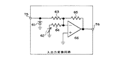
図3を用いて、入出力変換回路6の構成の例を説明する。入出力変換回路6は、定電圧ダイオード61と、可変電圧源62と、抵抗63,64,65と、演算増幅器66とを有して構成される。端子T5に加えられる電圧が定電圧ダイオード61で決められる電圧以下の電圧レベルで端子T6の出力レベルが上昇する構成になっている。
その特性は、平均映像レベル(APL)とAMP2,3の利得の関係を示す図4に示す特性と相似であり。縦軸がAMP利得の代わりに端子T6の出力電圧になる。
【0023】
以下、図1に示した液晶表示装置の動作を説明する。DEC1は、端子T11に印加された輝度信号Yおよび端子T12に印加された色信号Cをデコードして色差信号B−Yと色差信号R−Yを出力する。この色差信号B−Y,R−Yは、それぞれAMP2,3に入力され振幅を可変増幅された後、DEC4に入力される。さらにDEC4には、輝度信号Yも入力されており、色差信号B−Y,R−Yと輝度信号Yをマトリクス演算して、RGB原色信号を出力する。このRGB原色信号はLCD8に入力され所望の画像を表示する。制御回路7は端子T13に印加された水平同期信号Hと、端子T14に印加された垂直同期信号Vに基づきLCD8を駆動するために必要なタイミング信号を生成する。
【0024】
一方、APL検出手段5は、輝度信号Yの平均レベルを求めることで平均映像レベルを求め、入出力変換回路6で入出力特性を変換しAMP2,3の利得を制御する。
【0025】
平均映像レベル(APL)とAMP2,3の利得の関係を図4に示す。入出力変換回路6は、APLが低いときはAMP2,3のゲインを上げ、APLが高いときはAMP2,3のゲインを下げるように動作する。これにより色差信号B−Y,R−Yの振幅がAPLに応じて制御されることになる。
【0026】
ここで、図5を用いて、色差信号B−Y,R−Yと、色相、彩度の関係を説明する。図5は、横軸に色差信号B−Yの振幅を、縦軸に色差信号R−Y信号の振幅を示している。同図によれば、B−Y軸とR−Y軸の振幅から色相と彩度が一義的に決まることがわかる。これより、色差信号B−YとR−Yの振幅比を一定にしたまま振幅レベルを大きくすれば、色相を一定としたまま、彩度を上げることができる。したがって、図1に示したAMP2,3で同時に同じだけ利得を変更すことによって色相一定のまま彩度を変更することを可能にしている。
【0027】
また、DEC1およびDEC4は、例えば東芝製のカラーテレビ用ビデオ、クロマ、同期偏向回路システムLSI(TA1222AN)などで簡単に構成することができる。上記LSIでは色差信号としてI,Q信号が出力されている。I,Q信号は人の目の特性に合わせて色差信号R−Y,B−Y信号を補正したものであり、図1の色差信号R−Y,B−Yの代わりにI,Q信号を用いても良いことは言うまでもないことである。
【0028】
以上のようにして、APLに応じて彩度を可変することができ、APLが低いときに彩度を上げて、低輝度レベルでも映えのある映像表示画を得ることが可能になり、ブラウン管映像に匹敵するメリハリのある映像表示が実現できる。
【0029】
図6を用いて、本発明にかかる画像表示装置の第2の実施の形態を説明する。この実施の形態にかかる液晶表示装置は、入力信号がRGB原色信号である場合を示しており、エンコーダ(以下、ENCという)40と、DEC41を有している点が図1に示した第1の実施形態と異なっている。図1と同じ機能ブロックには同一番号を付して示す。
【0030】
図7を用いて、ENC40の構成の例を説明する。ENC40は、乗算器401R,401G,401B,402と、加算器405,406,407,408と、係数器403R,403G,403B,404とを有して構成される。
端子T40R,T40G,T40Bに印加されたRGB信号は、乗算器401R,401G,401Bで係数403R〜403Bが乗じられる。これら係数を乗じたRGB信号を加算器405,406で加算して輝度信号Yを生成する。
また、色差信号R−Yは加算器407で端子T40Rに印加されたR信号から輝度信号Yを減じて生成し、色差信号B−Yは加算器408で端子T40Bに印加されたB信号から輝度信号Yを減じて生成することができる。−Yは輝度信号Yに乗算器402で−1係数を乗じて生成すればよい。
【0031】
図8を用いて、DEC41の構成を説明する。DEC41は、乗算器411Y,411R,411Bと、係数器412Y,412R,412Bと、加算器413,414,415,416を有して構成される。
【0032】
端子T41Y,T41R,T41Bに印加された輝度信号Y、色差信号R−Y、色差信号B−Y信号は、乗算器411Y,411R,411Bで係数412Y,412R,412Bを乗じられ加算器413、414で加算してG信号を生成する。
また、R信号は加算器415で端子T41Rに印加された色差信号R−Yに輝度信号Yを加算して生成し、B信号は加算器416で端子T41Bに印加された色差信号B−Yに輝度信号Yを加算して生成することができる。
APL検出回路5、入出力変換回路6、AMP2,3の回路動作は、図1に示した第1の実施の形態と同様なので詳細説明は省略する。
【0033】
入力信号形態がRGB原色信号であっても、この実施の形態にかかる構成であればAPLを検出して色差信号R−Y,B−Yの利得を制御することができ、第1の実施の形態と同様にAPLに応じて彩度を可変とすることができる。これにより、APLが低いときに彩度を上げて低輝度レベルでも映えのある映像表示画が可能になり、ブラウン管映像に匹敵するメリハリのある映像表示が実現できる。
【0034】
図9を用いて、本発明にかかる画像表示装置の第3の実施の形態を説明する。この実施の形態にかかる液晶表示装置は、色相検出回路90と、切替器92と、可変電源91を有して構成される。そのほか図1に示した第1の実施の形態と同じ機能を有するブロックには同一番号を付して示す。
【0035】
本実施の形態の特徴は、色相検出回路90で特定の色相を検出し、その出力に基づいて、切替器92で入出力変換回路6への信号をAPL検出回路5の出力と可変電源91を切り替えることで、特定色相の色に対して彩度を上げるようにしたことにある。
【0036】
色相検出回路90と切替器92以外の動作は、図1に示した第1の実施の形態と同様なのでその説明は省略し、色相検出回路90の動作を中心に述べる。
【0037】
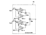
図10を用いて、色相検出回路90の構成の例を説明する。色相検出回路90は、比較器901−1,901−2,901−3,901−4と、比較用基準電源902−1,902−2,902−3,902−4と、乗算器903,904,905とを有して構成される。
【0038】
比較器901−1の出力は、端子T901に印加される色差信号B−Yが比較用基準電源902−1の設定電圧より大きいときに“1”小さいときに“0”となる。
比較器901−2の出力は、端子T901に印加される色差信号B−Yが比較用基準電源901−2の設定電圧より小さいときに“1”、大きいときに“0”となる。
そして、比較器901−1、901−2の出力は乗算器903で乗算され、比較器901−1、901−2両方が“1”のとき乗算器903の出力が“1”となる。すなわち比較用基準電源902−1<比較用基準電源902−2のとき、比較器901−1と901−2と乗算器903は端子T901に印加される色差信号B−Yに対し上記電圧範囲に感応するウィンドコンパレターとして動作する。
【0039】
端子T902に印加される色差信号R−Y信号に対しても比較器901−3,901−4、乗算器904は同様の動作をする。乗算器903と904の出力は乗算器905でさらに乗じられる。この結果、端子T901と端子T902に印加される色差信号B−Y,R−Yの信号レベルが特定範囲すなわち特定色相のとき、乗算器905から“1”が出力されることになる。
【0040】
図11を用いてこれを説明する。図11は横軸に色相、縦軸に振幅レベルをとり色差信号B−Y,R−Yをプロットしたものである。なお、振幅レベルは正規化している。
【0041】
ここで、図10に示した比較用電源901−2を振幅−0.5レベル相当に、比較用電源902−1を振幅−0.86レベル相当に、比較用電源902−4を振幅0.86レベル相当に、比較用電源902−3を振幅0.5レベル相当に、それぞれ設定すると、同図斜線で示した色相120°〜150°の範囲のときに図10の乗算器905から出力を得ることができる。乗算器905の出力は色相検出回路90の出力である。
【0042】
図9に示した切替器92は、入力色相検出回路90の出力が“1”のときAPL検出回路5の出力を選択し、色相検出回路90の出力が“0”のとき可変電源91の出力を選択する。
可変電源91の電圧は、AMP2,3の利得が“1”になるような電圧レベルに設定し、彩度を上げないように設定しておく。
【0043】
これにより、色相検出回路90で特定の色相を検出した場合にAPL検出回路5の出力が入出力変換回路6に入力され、そのときAPLが低ければ映像彩度を上げるように動作する。図19に示したようにRGB再現範囲の縮小はRGB同等でなく偏りがあるため、特定色相の彩度を上げる場合に本実施の形態が有効になる。
【0044】
このようにして、特定色相の彩度をAPLに応じて可変することができ、特定色相のAPLが低いときに彩度を上げて低輝度レベルでも映えのある映像表示画が可能になり、ブラウン管映像に匹敵するメリハリのある映像表示が実現できる。
【0045】
図12を用いて、本発明にかかる画像表示装置の第4の実施の形態を説明する。この実施の形態にかかる液晶表示装置は、図6で説明した第2実施の形態に、図9で説明した第3実施の形態の色相検出回路90と切替器92を組み合わせたもので、RGB原色信号が入力される場合の構成を示している。それぞれの機能ブロックの詳細は説明済みなのでここでは省略する。
【0046】
本実施の形態の構成によればRGB原色信号入力に対しても、特定色相の彩度をAPLに応じて可変することができ、特定色相のAPLが低いときに彩度を上げ、低輝度レベルでも映えのある映像表示画が可能になり、ブラウン管映像に匹敵するメリハリのある映像表示が実現できる。
【0047】
図13を用いて、本発明にかかる画像表示装置の第5の実施の形態を説明する。この実施の形態は、第1実施の形態にかかる液晶表示装置をディジタル化したものである。
この実施の形態にかかる液晶表示装置は、ディジタルデコーダ(DECと記す)1Dと、ディジタルデコーダ(DEC)4Dと、APL検出回路5Dと、入出力変換回路6Dと、制御回路7Dと、液晶表示デバイス(LCDと記す)8と、AD変換器96Y、96Cと、DA変換器96R、96G、96Bと、ディジタル乗算器21、31とを有して構成される。
【0048】
端子T11から入力された輝度信号YはAD変換器96YでAD変換され、端子T12から入力された色信号CはAD変換器96CでAD変換され、以降の回路で処理される。
また、DEC4DのディジタルRGB原色信号出力は、DA変換器96R〜96Bでアナログ信号に変換されLCD8に入力される。
【0049】
図14を用いて、APL(平均映像レベル)を検出するAPL検出回路5Dの構成の例を説明する。APL検出回路5Dは、乗算器5D1と、係数回路5D2と、加算器5D3と、レジスタ5D4と、ラッチ5D5とを有して構成される。端子T5D1に印加されたディジタル輝度信号Yを乗算器5D1で係数回路5D2に設定された係数で乗じる加算器5D3に入力する。
加算器5D3では乗算器5D1の出力とレジスタ5D4の出力を加算する。この加算結果は再度レジスタ5D4に戻される。このレジスタに戻す動作は累積動作にほかならず、例えば1000回の平均を求める場合は係数回路5D2の係数値を1/1000に設定しておき、加算器5D3とレジスタ5D4で1000回の累積を行う。1000回の累積後ラッチ5D5でラッチすることで平均輝度レベルとして端子T5D2に出力されることになる。
【0050】
入出変換回路6Dは例えばLUT(Look Up Table)などで構成すればよい(図示せず)。また、図1のAMP2,3に対応する回路を乗算器21,31とすればよく、APL検出回路5D、入出変換回路6D、乗算器21,31を含めた特性は図4と同等にすればよい。
【0051】
また、DEC1DおよびDEC4Dは、例えば東芝製のTV信号処理LSI(TC90A06F、TA8884AN)などで簡単に構成することができる。上記LSIでも色差信号としてI,Q信号が出力されている。第1実施の形態と同様にR−Y,B−Y信号の代わりにI,Q信号を用いても良いことは言うまでもないことである。
【0052】
本実施の形態ではAPL検出回路5D、入出変換回路6D、乗算器21,31がディジタル回路で構成されているためLSI化が容易であり、LSI化によるコストメリットを享受できて生産コストを低く抑えることが可能になる。
【0053】
このようにして、APLに応じて彩度を可変することができ、APLが低いときに彩度を上げて低輝度レベルでも映えのある映像表示画が可能になり、ブラウン管映像に匹敵するメリハリのある映像表示装置が低コスト実現できる。
【0054】
図15を用いて、本発明にかかる画像表示装置の第6の実施の形態を説明する。この実施の形態の液晶表示装置は、図6に示した第2の実施の形態の液晶表示装置をディジタル化したものである。この実施の形態の液晶表示装置は、AD変換器95R,95G,95Bと、ディジタルエンコーダ(ENCと記す)40Dと、ディジタルデコーダ(DECと記す)41Dとを有して構成され、そのほか図1および図13と同じ機能を有するブロックには同一番号を付して示している。
【0055】
ENC40Dは図7に示したENC40を、DEC41Dは図8に示したDEC41をそれぞれディジタル化すればく、基本的な構成は同じでよい。例えば、乗算器はディジタル乗算器に、加算器はディジタル加算器に、係数器はレジスタに置き換えれば良い。
本実施の形態では入力信号がディジタル化したRGB原色信号に対応する場合の構成を示している。もちろん、LSI化によるコストメリットを享受でき、生産コストを低く抑えることができる。
動作の詳細は図6および図13で説明したのでここでは省略する。
【0056】
このようにして、入力信号形態がRGB原色信号であっても本実施の構成であればAPLを検出して色差信号R−Y,B−Yの利得を制御することができ、APLに応じて彩度を可変することができ、APLが低いときに彩度を上げて低輝度レベルでも映えのある映像表示画が可能になり、ブラウン管映像に匹敵するメリハリのある映像表示装置を低コストで実現できる。
【0057】
図16を用いて、本発明にかかる画像表示装置の第7の実施の形態を説明する。この実施の形態にかかる液晶表示装置は、図9に示した第3実施の形態にかかる液晶表示装置をディジタル化したものである。この実施の形態にかかる液晶表示装置は、色相検出回路90Dと、切替器92と、設定レジスタ91Dとを有しており、そのほか図13と同じ働きを有する機能ブロックには同一番号を付している。
【0058】
本実施の形態の特徴は、色相検出回路90Dで特定の色相を検出し、その出力で切替器92でAPL検出回路5D出力と設定レジスタ91Dを切り替えることで、特定色相の色に対して彩度を上げるようにしたことにある。
【0059】
図17を用いて、色相検出回路90Dの構成の例を説明する。図17に示す色相検出回路90Dは、図10に示す色相検出回路90をディジタル化したもので、比較用基準電源902−1〜902−4の代わりに設定用レジスタ9D2−1〜9D2−4を用いている。もちろん比較器9D1−1〜9D1−4と、乗算器9D3,9D4,9D5はディジタルタイプに構成される。
【0060】
なお、この動作は図10および図12に示した色相検出回路90の動作と同じなので詳細説明は省略する。
この実施の形態によれば、図13に示した実施の形態と同様に、LSI化によるコストメリットを享受でき、生産コストを低く抑えることが可能になる。
【0061】
このようにして、特定色相の彩度をAPLに応じて可変することができ、特定色相でAPLが低いときに彩度を上げ、低輝度レベルでも映えのある映像表示画が可能になり、ブラウン管映像に匹敵するメリハリのある映像表示装置が低コストで実現できる。
【0062】
図18を用いて、本発明にかかる画像表示装置の第8の実施の形態を説明する。この実施の形態にかかる液晶表示装置は、図12に示した第4の実施の形態似かかるできる液晶表示装置をディジタル化したものである。色相検出回路90D等の説明は第3実施の形態の図16で説明済みなのでここでは省略する。
【0063】
本実施の形態でもLSI化によるコストメリットを享受でき、生産コストを低く抑えることが可能になる。
【0064】
この実施の形態の構成によれば、RGB原色信号入力に対しても、特定色相の彩度をAPLに応じて可変することができ、特定色相のAPLが低いときに彩度を上げ、低輝度レベルでも映えのある映像表示画が可能になり、ブラウン管映像に匹敵するメリハリのある映像表示装置を低コストで実現できる。
【0065】
なお、図13、図15、図16、図18の実施の形態では、DA変換器96R〜96Bでアナログ信号に変換してLCD8に印加したが、LCD8がディジタル入力可能なタイプであればディジタルRGB原色信号を入力しても良いことは言うまでもないことである。
【0066】
以上の実施の形態では、画像表示デバイスとしてLCDを用いた例を説明したが、画像表示デバイスは、LCDに限らず入力映像信号のレベルが変化することによって再現される画像の彩度が変化するおそれのある画像表示デバイスに適用することができる。これによれば、入力映像信号のレベルが変化しても、最適な画像を再現することができる。
【0067】
【発明の効果】
以上説明したように、本発明によれば、APLに応じて彩度を可変することができるので、低輝度レベルにおけるRGB色再現範囲の縮小現象を補償して、APLが低いときに彩度を上げて低輝度レベルでも映えのある、ブラウン管映像に匹敵する映像表示が実現できる。
【0068】
なお、本実施例の形態では液晶表示装置を主に説明したが、ブラウン管に替わる表示装置にはPDPやEL等様々あり、それらの表示デバイスでもRGB色再現範囲の縮小現象があれば、本発明が適用できその効果を享受できることは言うまでもないことである。
【図面の簡単な説明】
【図1】本発明にかかる画像表示装置の第1の実施の形態を示すブロック図。
【図2】図1に示すAPL検出回路の具体的な構成例を示す図。
【図3】図1に示す入出力変換回路の具体的な構成例を示す図。
【図4】APL対AMP利得の特性を示す図。
【図5】色相と彩度の関係を示す図。
【図6】本発明にかかる画像表示装置の第2の実施の形態を示すブロック図。
【図7】図6に示すENC回路の具体的な構成例を示すブロック図。
【図8】図6に示すDEC回路の具体的な構成例を示すブロック図。
【図9】本発明にかかる画像表示装置の第3の実施の形態を示すブロック図。
【図10】図9に示す色相検出回路の具体的な構成例を示すブロック図。
【図11】色差信号と色相の関係を示す図。
【図12】本発明にかかる画像表示装置の第4の実施の形態を示すブロック図。
【図13】本発明にかかる画像表示装置の第5の実施の形態を示すブロック図。
【図14】図13に示すAPL検出回路の具体的な構成例を示すブロック図。
【図15】本発明にかかる画像表示装置の第6の実施の形態を示すブロック図。
【図16】本発明にかかる画像表示装置の第7の実施の形態を示すブロック図。
【図17】図16に示す色相検出回路の具体的な構成例を示すブロック図。
【図18】本発明にかかる画像表示装置の第8の実施の形態を示すブロック図。
【図19】液晶表示装置のRGB色再現範囲の変化を示す図。
【図20】ブラウン管表示装置のRGB色再現範囲の変化を示す図。
【符号の説明】
1,1D デコーダ(DEC)
2,3 可変利得増幅器(AMP)
4,4D デコーダ(DEC)
5,5D APL(平均映像レベル)検出回路
6,6D 入出力変換回路
7,7D 制御回路
8 液晶表示装置(LCD)
21,31 乗算器
40D ディジタルエンコーダ(ENC)
41D ディジタルデコーダ(DEC)
90,90D 色相検出回路
91,91D 可変電圧源
92 切替器
95 AD変換器
96 DA変換器[0001]
BACKGROUND OF THE INVENTION
The present invention relates to an image display device such as a liquid crystal display, and relates to a saturation compensation technique in a state of displaying with low luminance.
[0002]
[Prior art]
In recent years, liquid crystal display devices such as front-projection LCD front projectors and rear-projection liquid crystal rear projectors that project images by enlarging and projecting PC screens to screens, and direct-view LCD monitors that are used as PC screen monitors on desktops It is rapidly spreading and is establishing its position as a display device after CRT.
[0003]
In general, a liquid crystal display device is said to have a wider color reproduction range and a better color reproducibility than a cathode ray tube compared to a cathode ray tube display device. Certainly, the high-intensity display on a liquid crystal projector has a colorful impression, and many presentations on a personal computer have a high impression. However, when a natural image such as a TV image is displayed, it may be dull and may not appear in the image.
[0004]
FIG. 19 is an example in which the maximum light emission luminance and the minimum light emission luminance of the RGB primary colors of the liquid crystal display device are equally divided and displayed on the chromaticity diagram. The gradation level at the maximum luminance is 1, and the minimum luminance is obtained. The gradation level is indicated by 0. As can be seen from the figure, in the liquid crystal display device, the RGB triangle becomes narrower as the gradation level decreases from 1 to 0.1.
On the other hand, FIG. 20 is an example of a chromaticity diagram of a cathode ray tube display device. As is clear from the figure, the RGB triangle of the CRT display device is hardly narrowed even when the gradation level is changed, as compared with the liquid crystal display device shown in FIG.
[0005]
As described above, the liquid crystal display device may have a wider RGB color reproduction range than the cathode ray tube display device at high luminance, but the range is reduced as the gradation level is reduced. This reduction of the color reproduction range lowers the pure color values of RGB, resulting in a decrease in saturation. That is, there is a problem in that the saturation is low at the low luminance level and the video is no longer visible.
[0006]
Usually, a television receiver or the like is equipped with a function for adjusting the saturation, referred to as color contrast for image adjustment, but the above problem is caused by the RGB color reproduction range changing according to the gradation level. Therefore, this adjustment function cannot solve this problem. In a liquid crystal display device, if the saturation is simply increased in order to cope with the decrease in saturation, the saturation of all gradation levels will increase, and the image will be glaring at high luminance. In a liquid crystal display device, it is necessary to increase the saturation only for the low luminance level in order to eliminate the deterioration of the image quality at the low luminance level.
[0007]
Japanese Patent Application Laid-Open No. 6-22174 discloses a video control circuit for reducing the noise feeling of a video in a region where the average picture level (APL) is low and increasing the effect of a selected video menu. Proposed. Since this circuit lowers the color level (color density) to some extent in an image with a low APL, the saturation of only the low luminance level cannot be increased.
[0008]
Japanese Patent Application Laid-Open No. 6-311396 discloses a method for compensating for the loss of details of a low-brightness signal when a high-brightness signal and a low-brightness signal are mixed in a video signal shot by a television camera or the like. It has been proposed to detect an average luminance level of a luminance video signal and control brightness and saturation by average luminance data obtained by correcting the average luminance level. This method can reproduce details of a low-luminance signal portion in a high-luminance signal image and has no effect on saturation. However, the low-luminance video signal lacks saturation. It is not considered to make up.
[0009]
Furthermore, in Japanese Patent Laid-Open No. Hei 8-2922752, as a brightness automatic adjustment device that performs appropriate screen adjustment according to the user's preference, the brightness value of the video signal is detected and the screen brightness of the display device is determined. It has been proposed to control the screen brightness to be high when the brightness of the video signal is too low. This method does not show increasing the saturation when the average video level is low.
[0010]
In addition, these proposals do not show increasing the saturation of a specific hue in a region where the average video level is low.
[0011]
[Problems to be solved by the invention]
An object of the present invention is to eliminate a reduction in saturation at a low luminance level in the above image display device and to reproduce a dull image with respect to a natural image such as a television image signal.
It is another object of the present invention to provide an image display device that increases the saturation of a specific hue and reproduces a sharp image when the average video level in the specific hue is low.
[0012]
[Means for Solving the Problems]
In order to solve the above-described problems, the present invention detects an average picture level (hereinafter referred to as APL) in a liquid crystal display device and increases the saturation of a video signal when the APL is low.
As a result, even when the screen is dark as a whole, the color saturation is increased and the image becomes more vivid and a sharp image display comparable to a CRT image can be realized.
[0013]
According to the present invention, in the image display device, the saturation of the video signal is changed according to the average video level of the input video signal.
[0014]
The present invention provides an image display apparatus comprising at least an average video level detection means for detecting an average video level of an input video signal and a video signal gain variable means for changing a gain of the input video signal. According to the average video level of the input video signal detected by the means, the gain of the video signal is controlled by the video signal gain varying means to change the saturation of the video signal.
[0015]
According to the present invention, in the above image display device, the video signal whose gain is controlled by the video signal gain varying means is a color difference signal.
[0016]
Further, according to the present invention, in the image display device, the saturation of the desired hue of the video signal is changed according to the average video level of the input video signal.
[0017]
The present invention includes at least an average video level detection unit that detects an average video level of an input video signal, a video signal gain variable unit that changes a gain of the input video signal, and a hue detection unit that detects a signal of a specific hue. In the image display apparatus, the gain of the video signal is adjusted with respect to the hue detected by the hue detection means by the video signal gain varying means according to the average video level of the input video signal detected by the average video level detection means. In addition to changing the saturation of the desired hue of the video signal, the video signal whose gain is controlled by the video signal gain varying means is used as the color difference signal.
[0018]
The present invention is characterized in that the image display device is a liquid crystal display device.
[0019]
DETAILED DESCRIPTION OF THE INVENTION
A first embodiment of an image display device according to the present invention will be described with reference to FIG. 1 as an example of a liquid crystal display device. The liquid crystal display device includes a decoder (hereinafter referred to as DEC) 1, a variable gain amplifier (hereinafter referred to as AMP) 2 and 3, DEC4, An
[0020]
DEC1 is a terminal T 11 Luminance signal Y input from the terminal T and the terminal T 12 The color difference signal BY and the color difference signal RY are generated from the color signal C input from. The
[0021]
An example of the configuration of the
The
[0022]
An example of the configuration of the input /
The characteristic is similar to the characteristic shown in FIG. 4 showing the relationship between the average video level (APL) and the gain of
[0023]
The operation of the liquid crystal display device shown in FIG. 1 will be described below. DEC1 is a terminal T 11 Luminance signal Y and terminal T applied to 12 The color signal C applied to is decoded and a color difference signal BY and a color difference signal RY are output. The color difference signals BY and RY are input to the
[0024]
On the other hand, the APL detection means 5 obtains the average video level by obtaining the average level of the luminance signal Y, converts the input / output characteristics by the input /
[0025]
FIG. 4 shows the relationship between the average video level (APL) and the gain of
[0026]
Here, the relationship between the color difference signals BY, RY, hue, and saturation will be described with reference to FIG. In FIG. 5, the horizontal axis indicates the amplitude of the color difference signal BY, and the vertical axis indicates the amplitude of the color difference signal RY signal. According to the figure, it can be seen that the hue and saturation are uniquely determined from the amplitudes of the BY axis and the RY axis. Accordingly, if the amplitude level is increased while the amplitude ratio between the color difference signals BY and RY is kept constant, the saturation can be increased while keeping the hue constant. Therefore, it is possible to change the saturation while keeping the hue constant by simultaneously changing the gain by the same amount in the
[0027]
Further, DEC1 and DEC4 can be easily configured by, for example, Toshiba color TV video, chroma, synchronous deflection circuit system LSI (TA1222AN), and the like. In the LSI, I and Q signals are output as color difference signals. The I and Q signals are obtained by correcting the color difference signals RY and BY in accordance with the characteristics of the human eye. Instead of the color difference signals RY and BY in FIG. It goes without saying that it may be used.
[0028]
As described above, the saturation can be varied according to the APL, and when the APL is low, the saturation can be increased to obtain a video display image that is brilliant even at a low luminance level. The image display with sharpness comparable to can be realized.
[0029]
A second embodiment of the image display apparatus according to the present invention will be described with reference to FIG. The liquid crystal display device according to this embodiment shows a case in which the input signal is an RGB primary color signal, and the first embodiment shown in FIG. 1 has an encoder (hereinafter referred to as ENC) 40 and a
[0030]
An example of the configuration of the
The RGB signals applied to the terminals T40R, T40G, and T40B are multiplied by
Further, the color difference signal RY is generated by subtracting the luminance signal Y from the R signal applied to the terminal T40R by the
[0031]
The configuration of the
[0032]
The luminance signal Y, the color difference signal RY, and the color difference signal BY applied to the terminals T41Y, T41R, and T41B are multiplied by
The R signal is generated by adding the luminance signal Y to the color difference signal RY applied to the terminal T41R by the
Since the circuit operations of the
[0033]
Even if the input signal form is an RGB primary color signal, the configuration according to this embodiment can detect the APL and control the gains of the color difference signals RY and BY. Similar to the form, the saturation can be made variable according to the APL. As a result, when the APL is low, it is possible to increase the saturation and display a vivid image even at a low luminance level, and to realize a sharp image display comparable to a CRT image.
[0034]
A third embodiment of the image display apparatus according to the present invention will be described with reference to FIG. The liquid crystal display device according to this embodiment includes a
[0035]
A feature of the present embodiment is that a
[0036]
Since the operations other than the
[0037]
An example of the configuration of the
[0038]
The output of the comparator 901-1 becomes “0” when the color difference signal BY applied to the terminal T901 is “1” smaller than the set voltage of the comparison reference power supply 902-1.
The output of the comparator 901-2 is “1” when the color difference signal BY applied to the terminal T901 is smaller than the set voltage of the comparison reference power supply 901-2, and becomes “0” when larger.
The outputs of the comparators 901-1 and 901-2 are multiplied by the
[0039]
The comparators 901-3 and 901-4 and the
[0040]
This will be described with reference to FIG. In FIG. 11, the color difference signals BY and RY are plotted with the hue on the horizontal axis and the amplitude level on the vertical axis. The amplitude level is normalized.
[0041]
Here, the comparison power source 901-2 shown in FIG. 10 corresponds to an amplitude of -0.5 level, the comparison power source 902-1 corresponds to an amplitude of -0.86 level, and the comparison power source 902-4 has an amplitude of .0. When the comparison power source 902-3 is set to have an amplitude of 0.5 level corresponding to 86 levels, the output from the
[0042]
The
The voltage of the
[0043]
As a result, when a specific hue is detected by the
[0044]
In this way, the saturation of the specific hue can be varied according to the APL, and when the APL of the specific hue is low, the saturation can be increased and a video display image can be displayed even at a low luminance level. A sharp image display comparable to the video can be realized.
[0045]
A fourth embodiment of the image display apparatus according to the present invention will be described with reference to FIG. The liquid crystal display device according to this embodiment is a combination of the second embodiment described with reference to FIG. 6 and the
[0046]
According to the configuration of the present embodiment, even for RGB primary color signal input, the saturation of a specific hue can be varied according to the APL, and when the APL of the specific hue is low, the saturation is increased and a low luminance level is obtained. However, a vivid video display image becomes possible, and a sharp video display comparable to a CRT video can be realized.
[0047]
A fifth embodiment of the image display apparatus according to the present invention will be described with reference to FIG. In this embodiment, the liquid crystal display device according to the first embodiment is digitized.
A liquid crystal display device according to this embodiment includes a digital decoder (denoted as DEC) 1D, a digital decoder (DEC) 4D, an
[0048]
The luminance signal Y input from the terminal T11 is AD-converted by the AD converter 96Y, and the color signal C input from the terminal T12 is AD-converted by the AD converter 96C and processed by the subsequent circuits.
Further, the digital RGB primary color signal output of DEC4D is converted into an analog signal by the
[0049]
An example of the configuration of the
The adder 5D3 adds the output of the multiplier 5D1 and the output of the register 5D4. The addition result is returned to the register 5D4 again. The operation of returning to this register is nothing but the accumulation operation. For example, when obtaining the average of 1000 times, the coefficient value of the coefficient circuit 5D2 is set to 1/1000, and the adder 5D3 and the register 5D4 accumulate 1000 times. . By latching by the latch 5D5 after accumulating 1000 times, the average luminance level is output to the terminal T5D2.
[0050]
The input /
[0051]
Further, DEC1D and DEC4D can be easily configured by, for example, a TV signal processing LSI (TC90A06F, TA8884AN) manufactured by Toshiba. In the LSI, I and Q signals are output as color difference signals. It goes without saying that I and Q signals may be used instead of the RY and BY signals as in the first embodiment.
[0052]
In the present embodiment, since the
[0053]
In this way, the saturation can be varied according to the APL, and when the APL is low, the saturation is increased and a vivid video display image is possible even at a low luminance level. A certain video display device can be realized at low cost.
[0054]
A sixth embodiment of the image display apparatus according to the present invention will be described with reference to FIG. The liquid crystal display device of this embodiment is a digitized version of the liquid crystal display device of the second embodiment shown in FIG. The liquid crystal display device of this embodiment is configured to include
[0055]
The ENC 40D is digitized from the
In the present embodiment, a configuration in which an input signal corresponds to a digitized RGB primary color signal is shown. Of course, it is possible to enjoy the cost merit of using LSI and to keep the production cost low.
Details of the operation have been described with reference to FIGS.
[0056]
Thus, even if the input signal form is an RGB primary color signal, the APL can be detected and the gains of the color difference signals RY and BY can be controlled with the configuration of the present embodiment. Saturation can be varied, and when APL is low, it is possible to increase the saturation and display a vivid image even at low luminance levels, realizing a sharp image display device comparable to a CRT image at a low cost. it can.
[0057]
A seventh embodiment of the image display apparatus according to the present invention will be described with reference to FIG. The liquid crystal display device according to this embodiment is a digitized version of the liquid crystal display device according to the third embodiment shown in FIG. The liquid crystal display device according to this embodiment includes a hue detection circuit 90D, a
[0058]
The feature of the present embodiment is that the hue detection circuit 90D detects a specific hue, and the
[0059]
An example of the configuration of the hue detection circuit 90D will be described with reference to FIG. The hue detection circuit 90D shown in FIG. 17 is a digitized version of the
[0060]
Since this operation is the same as that of the
According to this embodiment, as in the embodiment shown in FIG. 13, it is possible to enjoy the cost merit of using LSI and to keep the production cost low.
[0061]
In this way, the saturation of a specific hue can be varied according to the APL, the saturation is increased when the APL is low at a specific hue, and a vivid video display image is possible even at a low luminance level. A sharp video display device comparable to video can be realized at low cost.
[0062]
The eighth embodiment of the image display apparatus according to the present invention will be described with reference to FIG. The liquid crystal display device according to this embodiment is a digitized version of the liquid crystal display device according to the fourth embodiment shown in FIG. The description of the hue detection circuit 90D and the like has already been described with reference to FIG. 16 of the third embodiment, and is omitted here.
[0063]
Also in this embodiment, the cost merit by using LSI can be enjoyed, and the production cost can be kept low.
[0064]
According to the configuration of this embodiment, even for RGB primary color signal input, the saturation of a specific hue can be varied according to the APL, and when the APL of the specific hue is low, the saturation is increased and the luminance is low. This makes it possible to display video images that are brilliant even at the level, and realize a sharp video display device comparable to a CRT video at a low cost.
[0065]
In the embodiments of FIGS. 13, 15, 16, and 18, the
[0066]
In the above embodiments, an example in which an LCD is used as an image display device has been described. However, the image display device is not limited to an LCD, and the saturation of an image to be reproduced changes when the level of an input video signal changes. The present invention can be applied to an image display device having a fear. According to this, even if the level of the input video signal changes, an optimal image can be reproduced.
[0067]
【The invention's effect】
As described above, according to the present invention, the saturation can be varied according to the APL, so that the reduction phenomenon of the RGB color reproduction range at the low luminance level is compensated, and the saturation is reduced when the APL is low. It is possible to realize a video display comparable to a CRT picture, which can be raised and shine even at low luminance levels.
[0068]
Although the liquid crystal display device has been mainly described in the form of the present embodiment, there are various display devices such as PDP and EL that can be used instead of the cathode ray tube. It goes without saying that can be applied and enjoy its effects.
[Brief description of the drawings]
FIG. 1 is a block diagram showing a first embodiment of an image display apparatus according to the present invention.
FIG. 2 is a diagram showing a specific configuration example of an APL detection circuit shown in FIG. 1;
FIG. 3 is a diagram showing a specific configuration example of the input / output conversion circuit shown in FIG. 1;
FIG. 4 is a diagram showing characteristics of APL vs. AMP gain.
FIG. 5 is a diagram illustrating a relationship between hue and saturation.
FIG. 6 is a block diagram showing a second embodiment of an image display device according to the present invention.
7 is a block diagram illustrating a specific configuration example of an ENC circuit illustrated in FIG. 6;
8 is a block diagram illustrating a specific configuration example of the DEC circuit illustrated in FIG. 6;
FIG. 9 is a block diagram showing a third embodiment of an image display apparatus according to the present invention.
10 is a block diagram illustrating a specific configuration example of a hue detection circuit illustrated in FIG. 9;
FIG. 11 is a diagram illustrating a relationship between a color difference signal and a hue.
FIG. 12 is a block diagram showing a fourth embodiment of an image display apparatus according to the present invention.
FIG. 13 is a block diagram showing a fifth embodiment of an image display apparatus according to the present invention.
14 is a block diagram showing a specific configuration example of the APL detection circuit shown in FIG. 13;
FIG. 15 is a block diagram showing a sixth embodiment of an image display apparatus according to the present invention.
FIG. 16 is a block diagram showing a seventh embodiment of an image display apparatus according to the present invention.
FIG. 17 is a block diagram showing a specific configuration example of the hue detection circuit shown in FIG. 16;
FIG. 18 is a block diagram showing an eighth embodiment of an image display apparatus according to the present invention.
FIG. 19 is a diagram showing a change in the RGB color reproduction range of the liquid crystal display device.
FIG. 20 is a diagram showing a change in RGB color reproduction range of a CRT display device.
[Explanation of symbols]
1,1D decoder (DEC)
2,3 Variable gain amplifier (AMP)
4,4D decoder (DEC)
5,5D APL (average video level) detection circuit
6,6D input / output conversion circuit
7,7D control circuit
8 Liquid crystal display (LCD)
21,31 multiplier
40D digital encoder (ENC)
41D digital decoder (DEC)
90,90D hue detection circuit
91, 91D Variable voltage source
92 switcher
95 AD converter
96 DA converter
Claims (9)
入力される映像信号の平均輝度レベルに応じて色再現範囲が変化する特性を持つ表示デバイスと、
前記映像信号の平均輝度レベルを得るための手段と、
前記得られた映像信号の平均輝度レベルが所定値よりも低いときに、前記映像信号の平均輝度レベルの減少に応じてその映像信号の彩度を順次増加させる手段と、を備え、
前記表示デバイスは、前記彩度が増加された信号に基づき前記色再現範囲の変化が抑制された映像を表示することを特徴とする画像表示装置。In an image display device,
A display device having a characteristic that the color reproduction range changes according to the average luminance level of the input video signal;
And means for obtaining an average luminance level of the video signal,
When the average luminance level of the obtained video signal is lower than a predetermined value, and means for increasing the saturation of the video signal sequentially in response to a decrease of the average luminance level of the video signal,
The image display device, wherein the display device displays an image in which a change in the color reproduction range is suppressed based on the signal with increased saturation.
入力される映像信号の平均輝度レベルの減少とともに色再現範囲が縮小する特性を持つ表示デバイスと、
前記映像信号の平均輝度レベルを得るための手段と、
前記得られた映像信号の平均輝度レベルが所定の値よりも低いときに前記映像信号の平均輝度レベルが低い程その映像信号の彩度を増加させる手段と、を備え、
前記表示デバイスは、前記彩度が制御された信号に基づき前記色再現範囲の変化が抑制された映像を表示することを特徴とする画像表示装置。In an image display device,
A display device having a characteristic that the color reproduction range is reduced as the average luminance level of the input video signal is reduced;
And means for obtaining an average luminance level of the video signal,
And means for increasing the saturation of the lower the average luminance level of the video signal the video signal when less than the average luminance level is a predetermined value of the obtained video signal,
The image display apparatus, wherein the display device displays an image in which a change in the color reproduction range is suppressed based on the signal whose saturation is controlled.
前記輝度に関する情報を検出するための手段は、前記信号生成手段で生成された前記輝度信号Yを用いて該映像信号の平均輝度レベルを得るようにし、
前記彩度を制御する手段は、信号生成手段で生成された前記色差信号B−Y及びR−Yの振幅を制御することによって、前記映像信号の彩度を制御することを特徴とする画像表示装置。5. The image display device according to claim 1, further comprising signal generation means for generating color difference signals BY and RY and a luminance signal Y from the input video signal,
The means for detecting information relating to the brightness obtains an average brightness level of the video signal using the brightness signal Y generated by the signal generation means,
The means for controlling the saturation controls the saturation of the video signal by controlling the amplitude of the color difference signals BY and RY generated by the signal generation means. apparatus.
Priority Applications (1)
| Application Number | Priority Date | Filing Date | Title |
|---|---|---|---|
| JP20931598A JP4011743B2 (en) | 1998-07-24 | 1998-07-24 | Image display device |
Applications Claiming Priority (1)
| Application Number | Priority Date | Filing Date | Title |
|---|---|---|---|
| JP20931598A JP4011743B2 (en) | 1998-07-24 | 1998-07-24 | Image display device |
Related Child Applications (1)
| Application Number | Title | Priority Date | Filing Date |
|---|---|---|---|
| JP2005038564A Division JP2005198338A (en) | 2005-02-16 | 2005-02-16 | Image display apparatus |
Publications (3)
| Publication Number | Publication Date |
|---|---|
| JP2000039862A JP2000039862A (en) | 2000-02-08 |
| JP2000039862A5 JP2000039862A5 (en) | 2005-08-25 |
| JP4011743B2 true JP4011743B2 (en) | 2007-11-21 |
Family
ID=16570925
Family Applications (1)
| Application Number | Title | Priority Date | Filing Date |
|---|---|---|---|
| JP20931598A Expired - Fee Related JP4011743B2 (en) | 1998-07-24 | 1998-07-24 | Image display device |
Country Status (1)
| Country | Link |
|---|---|
| JP (1) | JP4011743B2 (en) |
Families Citing this family (9)
| Publication number | Priority date | Publication date | Assignee | Title |
|---|---|---|---|---|
| JP3580732B2 (en) * | 1999-06-30 | 2004-10-27 | 富士通株式会社 | Plasma display panel to keep color temperature or color deviation constant |
| JP3634730B2 (en) * | 2000-09-18 | 2005-03-30 | 三洋電機株式会社 | Tonal correction circuit and hue correction circuit |
| JP2002132225A (en) * | 2000-10-24 | 2002-05-09 | Sharp Corp | Video signal corrector and multimedia computer system using the same |
| KR100806903B1 (en) | 2001-09-27 | 2008-02-22 | 삼성전자주식회사 | Liquid crystal display and method for driving thereof |
| WO2005043502A1 (en) * | 2003-10-30 | 2005-05-12 | Matsushita Electric Industrial Co., Ltd. | Display apparatus, display method, program and recording medium |
| JP4648071B2 (en) * | 2005-04-28 | 2011-03-09 | 株式会社日立製作所 | Video display device and video signal color saturation control method |
| JP2007241225A (en) * | 2005-06-16 | 2007-09-20 | Toshiba Matsushita Display Technology Co Ltd | Driving method of display device using organic light emitting element and driving circuit of same |
| JP5023024B2 (en) | 2007-09-06 | 2012-09-12 | ミツミ電機株式会社 | Color correction circuit and image display apparatus using the same |
| KR102083299B1 (en) | 2013-09-02 | 2020-03-03 | 엘지전자 주식회사 | Display device and luminance control method thereof |
-
1998
- 1998-07-24 JP JP20931598A patent/JP4011743B2/en not_active Expired - Fee Related
Also Published As
| Publication number | Publication date |
|---|---|
| JP2000039862A (en) | 2000-02-08 |
Similar Documents
| Publication | Publication Date | Title |
|---|---|---|
| US5546134A (en) | Video brightness/contrast enhancement method adaptive to a scene and circuit therefor | |
| JP4271978B2 (en) | Video display device | |
| JP3719411B2 (en) | Image display system, projector, program, information storage medium, and image processing method | |
| JP4802350B2 (en) | Display device | |
| JP4419933B2 (en) | Image processing apparatus, image display apparatus, and image processing method | |
| JP2000013814A (en) | Video signal processing circuit | |
| EP1265219A1 (en) | Environment adaptive image display system, image processing method and information storing medium | |
| JP4967454B2 (en) | Image correction circuit, image correction method, and image display apparatus | |
| JP3134784B2 (en) | Image synthesis circuit | |
| JP4011743B2 (en) | Image display device | |
| JP2784839B2 (en) | Image signal gradation correction device | |
| JP2007311889A (en) | Image correction circuit, image correction method, and image display apparatus | |
| JP4659272B2 (en) | Tone correction device | |
| JPH11305734A (en) | Liquid crystal display device | |
| KR100228607B1 (en) | Color image display apparatus and color camera | |
| JP2003348377A (en) | Image display device and image processing apparatus, and image processing method | |
| JP2001296831A (en) | Picture reproducing method | |
| JPH06350943A (en) | Picture processing circuit | |
| JP2005198338A (en) | Image display apparatus | |
| JP2000354250A (en) | Image pickup device | |
| JPH0374969A (en) | Display device | |
| JP2002044679A (en) | Image signal processing circuit | |
| JP2935389B2 (en) | Video signal processing device and nonlinear signal processing device | |
| JP3531015B2 (en) | Video display device | |
| US6580464B1 (en) | Color difference signal correction apparatus |
Legal Events
| Date | Code | Title | Description |
|---|---|---|---|
| A521 | Written amendment |
Free format text: JAPANESE INTERMEDIATE CODE: A523 Effective date: 20050216 |
|
| A621 | Written request for application examination |
Free format text: JAPANESE INTERMEDIATE CODE: A621 Effective date: 20050216 |
|
| RD02 | Notification of acceptance of power of attorney |
Free format text: JAPANESE INTERMEDIATE CODE: A7422 Effective date: 20050216 |
|
| A131 | Notification of reasons for refusal |
Free format text: JAPANESE INTERMEDIATE CODE: A131 Effective date: 20060801 |
|
| A521 | Written amendment |
Free format text: JAPANESE INTERMEDIATE CODE: A523 Effective date: 20060928 |
|
| A131 | Notification of reasons for refusal |
Free format text: JAPANESE INTERMEDIATE CODE: A131 Effective date: 20070417 |
|
| A521 | Written amendment |
Free format text: JAPANESE INTERMEDIATE CODE: A523 Effective date: 20070614 |
|
| TRDD | Decision of grant or rejection written | ||
| A01 | Written decision to grant a patent or to grant a registration (utility model) |
Free format text: JAPANESE INTERMEDIATE CODE: A01 Effective date: 20070904 |
|
| A61 | First payment of annual fees (during grant procedure) |
Free format text: JAPANESE INTERMEDIATE CODE: A61 Effective date: 20070906 |
|
| R150 | Certificate of patent or registration of utility model |
Free format text: JAPANESE INTERMEDIATE CODE: R150 |
|
| FPAY | Renewal fee payment (event date is renewal date of database) |
Free format text: PAYMENT UNTIL: 20100914 Year of fee payment: 3 |
|
| FPAY | Renewal fee payment (event date is renewal date of database) |
Free format text: PAYMENT UNTIL: 20100914 Year of fee payment: 3 |
|
| FPAY | Renewal fee payment (event date is renewal date of database) |
Free format text: PAYMENT UNTIL: 20110914 Year of fee payment: 4 |
|
| FPAY | Renewal fee payment (event date is renewal date of database) |
Free format text: PAYMENT UNTIL: 20120914 Year of fee payment: 5 |
|
| LAPS | Cancellation because of no payment of annual fees |