JP4009056B2 - Power module - Google Patents
Power module Download PDFInfo
- Publication number
- JP4009056B2 JP4009056B2 JP2000154600A JP2000154600A JP4009056B2 JP 4009056 B2 JP4009056 B2 JP 4009056B2 JP 2000154600 A JP2000154600 A JP 2000154600A JP 2000154600 A JP2000154600 A JP 2000154600A JP 4009056 B2 JP4009056 B2 JP 4009056B2
- Authority
- JP
- Japan
- Prior art keywords
- power module
- heat sink
- power
- electrode
- semiconductor element
- Prior art date
- Legal status (The legal status is an assumption and is not a legal conclusion. Google has not performed a legal analysis and makes no representation as to the accuracy of the status listed.)
- Expired - Fee Related
Links
Images


Classifications
-
- H—ELECTRICITY
- H01—ELECTRIC ELEMENTS
- H01L—SEMICONDUCTOR DEVICES NOT COVERED BY CLASS H10
- H01L24/00—Arrangements for connecting or disconnecting semiconductor or solid-state bodies; Methods or apparatus related thereto
- H01L24/01—Means for bonding being attached to, or being formed on, the surface to be connected, e.g. chip-to-package, die-attach, "first-level" interconnects; Manufacturing methods related thereto
- H01L24/42—Wire connectors; Manufacturing methods related thereto
- H01L24/47—Structure, shape, material or disposition of the wire connectors after the connecting process
- H01L24/49—Structure, shape, material or disposition of the wire connectors after the connecting process of a plurality of wire connectors
-
- H—ELECTRICITY
- H01—ELECTRIC ELEMENTS
- H01L—SEMICONDUCTOR DEVICES NOT COVERED BY CLASS H10
- H01L23/00—Details of semiconductor or other solid state devices
- H01L23/34—Arrangements for cooling, heating, ventilating or temperature compensation ; Temperature sensing arrangements
- H01L23/46—Arrangements for cooling, heating, ventilating or temperature compensation ; Temperature sensing arrangements involving the transfer of heat by flowing fluids
- H01L23/473—Arrangements for cooling, heating, ventilating or temperature compensation ; Temperature sensing arrangements involving the transfer of heat by flowing fluids by flowing liquids
-
- H—ELECTRICITY
- H01—ELECTRIC ELEMENTS
- H01L—SEMICONDUCTOR DEVICES NOT COVERED BY CLASS H10
- H01L25/00—Assemblies consisting of a plurality of individual semiconductor or other solid state devices ; Multistep manufacturing processes thereof
- H01L25/03—Assemblies consisting of a plurality of individual semiconductor or other solid state devices ; Multistep manufacturing processes thereof all the devices being of a type provided for in the same subgroup of groups H01L27/00 - H01L33/00, or in a single subclass of H10K, H10N, e.g. assemblies of rectifier diodes
- H01L25/04—Assemblies consisting of a plurality of individual semiconductor or other solid state devices ; Multistep manufacturing processes thereof all the devices being of a type provided for in the same subgroup of groups H01L27/00 - H01L33/00, or in a single subclass of H10K, H10N, e.g. assemblies of rectifier diodes the devices not having separate containers
- H01L25/07—Assemblies consisting of a plurality of individual semiconductor or other solid state devices ; Multistep manufacturing processes thereof all the devices being of a type provided for in the same subgroup of groups H01L27/00 - H01L33/00, or in a single subclass of H10K, H10N, e.g. assemblies of rectifier diodes the devices not having separate containers the devices being of a type provided for in group H01L29/00
- H01L25/072—Assemblies consisting of a plurality of individual semiconductor or other solid state devices ; Multistep manufacturing processes thereof all the devices being of a type provided for in the same subgroup of groups H01L27/00 - H01L33/00, or in a single subclass of H10K, H10N, e.g. assemblies of rectifier diodes the devices not having separate containers the devices being of a type provided for in group H01L29/00 the devices being arranged next to each other
-
- H—ELECTRICITY
- H05—ELECTRIC TECHNIQUES NOT OTHERWISE PROVIDED FOR
- H05K—PRINTED CIRCUITS; CASINGS OR CONSTRUCTIONAL DETAILS OF ELECTRIC APPARATUS; MANUFACTURE OF ASSEMBLAGES OF ELECTRICAL COMPONENTS
- H05K7/00—Constructional details common to different types of electric apparatus
- H05K7/14—Mounting supporting structure in casing or on frame or rack
- H05K7/1422—Printed circuit boards receptacles, e.g. stacked structures, electronic circuit modules or box like frames
- H05K7/1427—Housings
- H05K7/1432—Housings specially adapted for power drive units or power converters
- H05K7/14329—Housings specially adapted for power drive units or power converters specially adapted for the configuration of power bus bars
-
- H—ELECTRICITY
- H01—ELECTRIC ELEMENTS
- H01L—SEMICONDUCTOR DEVICES NOT COVERED BY CLASS H10
- H01L2223/00—Details relating to semiconductor or other solid state devices covered by the group H01L23/00
- H01L2223/58—Structural electrical arrangements for semiconductor devices not otherwise provided for
- H01L2223/64—Impedance arrangements
- H01L2223/66—High-frequency adaptations
- H01L2223/6605—High-frequency electrical connections
- H01L2223/6616—Vertical connections, e.g. vias
- H01L2223/6622—Coaxial feed-throughs in active or passive substrates
-
- H—ELECTRICITY
- H01—ELECTRIC ELEMENTS
- H01L—SEMICONDUCTOR DEVICES NOT COVERED BY CLASS H10
- H01L2224/00—Indexing scheme for arrangements for connecting or disconnecting semiconductor or solid-state bodies and methods related thereto as covered by H01L24/00
- H01L2224/01—Means for bonding being attached to, or being formed on, the surface to be connected, e.g. chip-to-package, die-attach, "first-level" interconnects; Manufacturing methods related thereto
- H01L2224/42—Wire connectors; Manufacturing methods related thereto
- H01L2224/47—Structure, shape, material or disposition of the wire connectors after the connecting process
- H01L2224/48—Structure, shape, material or disposition of the wire connectors after the connecting process of an individual wire connector
- H01L2224/4805—Shape
- H01L2224/4809—Loop shape
- H01L2224/48091—Arched
-
- H—ELECTRICITY
- H01—ELECTRIC ELEMENTS
- H01L—SEMICONDUCTOR DEVICES NOT COVERED BY CLASS H10
- H01L2224/00—Indexing scheme for arrangements for connecting or disconnecting semiconductor or solid-state bodies and methods related thereto as covered by H01L24/00
- H01L2224/01—Means for bonding being attached to, or being formed on, the surface to be connected, e.g. chip-to-package, die-attach, "first-level" interconnects; Manufacturing methods related thereto
- H01L2224/42—Wire connectors; Manufacturing methods related thereto
- H01L2224/47—Structure, shape, material or disposition of the wire connectors after the connecting process
- H01L2224/48—Structure, shape, material or disposition of the wire connectors after the connecting process of an individual wire connector
- H01L2224/481—Disposition
- H01L2224/48135—Connecting between different semiconductor or solid-state bodies, i.e. chip-to-chip
- H01L2224/48137—Connecting between different semiconductor or solid-state bodies, i.e. chip-to-chip the bodies being arranged next to each other, e.g. on a common substrate
- H01L2224/48139—Connecting between different semiconductor or solid-state bodies, i.e. chip-to-chip the bodies being arranged next to each other, e.g. on a common substrate with an intermediate bond, e.g. continuous wire daisy chain
-
- H—ELECTRICITY
- H01—ELECTRIC ELEMENTS
- H01L—SEMICONDUCTOR DEVICES NOT COVERED BY CLASS H10
- H01L2224/00—Indexing scheme for arrangements for connecting or disconnecting semiconductor or solid-state bodies and methods related thereto as covered by H01L24/00
- H01L2224/01—Means for bonding being attached to, or being formed on, the surface to be connected, e.g. chip-to-package, die-attach, "first-level" interconnects; Manufacturing methods related thereto
- H01L2224/42—Wire connectors; Manufacturing methods related thereto
- H01L2224/47—Structure, shape, material or disposition of the wire connectors after the connecting process
- H01L2224/48—Structure, shape, material or disposition of the wire connectors after the connecting process of an individual wire connector
- H01L2224/481—Disposition
- H01L2224/48151—Connecting between a semiconductor or solid-state body and an item not being a semiconductor or solid-state body, e.g. chip-to-substrate, chip-to-passive
- H01L2224/48221—Connecting between a semiconductor or solid-state body and an item not being a semiconductor or solid-state body, e.g. chip-to-substrate, chip-to-passive the body and the item being stacked
- H01L2224/48225—Connecting between a semiconductor or solid-state body and an item not being a semiconductor or solid-state body, e.g. chip-to-substrate, chip-to-passive the body and the item being stacked the item being non-metallic, e.g. insulating substrate with or without metallisation
- H01L2224/48227—Connecting between a semiconductor or solid-state body and an item not being a semiconductor or solid-state body, e.g. chip-to-substrate, chip-to-passive the body and the item being stacked the item being non-metallic, e.g. insulating substrate with or without metallisation connecting the wire to a bond pad of the item
-
- H—ELECTRICITY
- H01—ELECTRIC ELEMENTS
- H01L—SEMICONDUCTOR DEVICES NOT COVERED BY CLASS H10
- H01L2224/00—Indexing scheme for arrangements for connecting or disconnecting semiconductor or solid-state bodies and methods related thereto as covered by H01L24/00
- H01L2224/01—Means for bonding being attached to, or being formed on, the surface to be connected, e.g. chip-to-package, die-attach, "first-level" interconnects; Manufacturing methods related thereto
- H01L2224/42—Wire connectors; Manufacturing methods related thereto
- H01L2224/47—Structure, shape, material or disposition of the wire connectors after the connecting process
- H01L2224/48—Structure, shape, material or disposition of the wire connectors after the connecting process of an individual wire connector
- H01L2224/481—Disposition
- H01L2224/48151—Connecting between a semiconductor or solid-state body and an item not being a semiconductor or solid-state body, e.g. chip-to-substrate, chip-to-passive
- H01L2224/48221—Connecting between a semiconductor or solid-state body and an item not being a semiconductor or solid-state body, e.g. chip-to-substrate, chip-to-passive the body and the item being stacked
- H01L2224/48225—Connecting between a semiconductor or solid-state body and an item not being a semiconductor or solid-state body, e.g. chip-to-substrate, chip-to-passive the body and the item being stacked the item being non-metallic, e.g. insulating substrate with or without metallisation
- H01L2224/4824—Connecting between the body and an opposite side of the item with respect to the body
-
- H—ELECTRICITY
- H01—ELECTRIC ELEMENTS
- H01L—SEMICONDUCTOR DEVICES NOT COVERED BY CLASS H10
- H01L2224/00—Indexing scheme for arrangements for connecting or disconnecting semiconductor or solid-state bodies and methods related thereto as covered by H01L24/00
- H01L2224/01—Means for bonding being attached to, or being formed on, the surface to be connected, e.g. chip-to-package, die-attach, "first-level" interconnects; Manufacturing methods related thereto
- H01L2224/42—Wire connectors; Manufacturing methods related thereto
- H01L2224/47—Structure, shape, material or disposition of the wire connectors after the connecting process
- H01L2224/48—Structure, shape, material or disposition of the wire connectors after the connecting process of an individual wire connector
- H01L2224/484—Connecting portions
- H01L2224/4847—Connecting portions the connecting portion on the bonding area of the semiconductor or solid-state body being a wedge bond
- H01L2224/48472—Connecting portions the connecting portion on the bonding area of the semiconductor or solid-state body being a wedge bond the other connecting portion not on the bonding area also being a wedge bond, i.e. wedge-to-wedge
-
- H—ELECTRICITY
- H01—ELECTRIC ELEMENTS
- H01L—SEMICONDUCTOR DEVICES NOT COVERED BY CLASS H10
- H01L2224/00—Indexing scheme for arrangements for connecting or disconnecting semiconductor or solid-state bodies and methods related thereto as covered by H01L24/00
- H01L2224/01—Means for bonding being attached to, or being formed on, the surface to be connected, e.g. chip-to-package, die-attach, "first-level" interconnects; Manufacturing methods related thereto
- H01L2224/42—Wire connectors; Manufacturing methods related thereto
- H01L2224/47—Structure, shape, material or disposition of the wire connectors after the connecting process
- H01L2224/49—Structure, shape, material or disposition of the wire connectors after the connecting process of a plurality of wire connectors
- H01L2224/491—Disposition
- H01L2224/4911—Disposition the connectors being bonded to at least one common bonding area, e.g. daisy chain
- H01L2224/49111—Disposition the connectors being bonded to at least one common bonding area, e.g. daisy chain the connectors connecting two common bonding areas, e.g. Litz or braid wires
-
- H—ELECTRICITY
- H01—ELECTRIC ELEMENTS
- H01L—SEMICONDUCTOR DEVICES NOT COVERED BY CLASS H10
- H01L2224/00—Indexing scheme for arrangements for connecting or disconnecting semiconductor or solid-state bodies and methods related thereto as covered by H01L24/00
- H01L2224/01—Means for bonding being attached to, or being formed on, the surface to be connected, e.g. chip-to-package, die-attach, "first-level" interconnects; Manufacturing methods related thereto
- H01L2224/42—Wire connectors; Manufacturing methods related thereto
- H01L2224/47—Structure, shape, material or disposition of the wire connectors after the connecting process
- H01L2224/49—Structure, shape, material or disposition of the wire connectors after the connecting process of a plurality of wire connectors
- H01L2224/491—Disposition
- H01L2224/4912—Layout
- H01L2224/49175—Parallel arrangements
-
- H—ELECTRICITY
- H01—ELECTRIC ELEMENTS
- H01L—SEMICONDUCTOR DEVICES NOT COVERED BY CLASS H10
- H01L24/00—Arrangements for connecting or disconnecting semiconductor or solid-state bodies; Methods or apparatus related thereto
- H01L24/01—Means for bonding being attached to, or being formed on, the surface to be connected, e.g. chip-to-package, die-attach, "first-level" interconnects; Manufacturing methods related thereto
- H01L24/42—Wire connectors; Manufacturing methods related thereto
- H01L24/47—Structure, shape, material or disposition of the wire connectors after the connecting process
- H01L24/48—Structure, shape, material or disposition of the wire connectors after the connecting process of an individual wire connector
-
- H—ELECTRICITY
- H01—ELECTRIC ELEMENTS
- H01L—SEMICONDUCTOR DEVICES NOT COVERED BY CLASS H10
- H01L2924/00—Indexing scheme for arrangements or methods for connecting or disconnecting semiconductor or solid-state bodies as covered by H01L24/00
- H01L2924/0001—Technical content checked by a classifier
- H01L2924/00014—Technical content checked by a classifier the subject-matter covered by the group, the symbol of which is combined with the symbol of this group, being disclosed without further technical details
-
- H—ELECTRICITY
- H01—ELECTRIC ELEMENTS
- H01L—SEMICONDUCTOR DEVICES NOT COVERED BY CLASS H10
- H01L2924/00—Indexing scheme for arrangements or methods for connecting or disconnecting semiconductor or solid-state bodies as covered by H01L24/00
- H01L2924/01—Chemical elements
- H01L2924/01004—Beryllium [Be]
-
- H—ELECTRICITY
- H01—ELECTRIC ELEMENTS
- H01L—SEMICONDUCTOR DEVICES NOT COVERED BY CLASS H10
- H01L2924/00—Indexing scheme for arrangements or methods for connecting or disconnecting semiconductor or solid-state bodies as covered by H01L24/00
- H01L2924/01—Chemical elements
- H01L2924/01005—Boron [B]
-
- H—ELECTRICITY
- H01—ELECTRIC ELEMENTS
- H01L—SEMICONDUCTOR DEVICES NOT COVERED BY CLASS H10
- H01L2924/00—Indexing scheme for arrangements or methods for connecting or disconnecting semiconductor or solid-state bodies as covered by H01L24/00
- H01L2924/01—Chemical elements
- H01L2924/01006—Carbon [C]
-
- H—ELECTRICITY
- H01—ELECTRIC ELEMENTS
- H01L—SEMICONDUCTOR DEVICES NOT COVERED BY CLASS H10
- H01L2924/00—Indexing scheme for arrangements or methods for connecting or disconnecting semiconductor or solid-state bodies as covered by H01L24/00
- H01L2924/01—Chemical elements
- H01L2924/01013—Aluminum [Al]
-
- H—ELECTRICITY
- H01—ELECTRIC ELEMENTS
- H01L—SEMICONDUCTOR DEVICES NOT COVERED BY CLASS H10
- H01L2924/00—Indexing scheme for arrangements or methods for connecting or disconnecting semiconductor or solid-state bodies as covered by H01L24/00
- H01L2924/01—Chemical elements
- H01L2924/01014—Silicon [Si]
-
- H—ELECTRICITY
- H01—ELECTRIC ELEMENTS
- H01L—SEMICONDUCTOR DEVICES NOT COVERED BY CLASS H10
- H01L2924/00—Indexing scheme for arrangements or methods for connecting or disconnecting semiconductor or solid-state bodies as covered by H01L24/00
- H01L2924/01—Chemical elements
- H01L2924/01016—Sulfur [S]
-
- H—ELECTRICITY
- H01—ELECTRIC ELEMENTS
- H01L—SEMICONDUCTOR DEVICES NOT COVERED BY CLASS H10
- H01L2924/00—Indexing scheme for arrangements or methods for connecting or disconnecting semiconductor or solid-state bodies as covered by H01L24/00
- H01L2924/01—Chemical elements
- H01L2924/01029—Copper [Cu]
-
- H—ELECTRICITY
- H01—ELECTRIC ELEMENTS
- H01L—SEMICONDUCTOR DEVICES NOT COVERED BY CLASS H10
- H01L2924/00—Indexing scheme for arrangements or methods for connecting or disconnecting semiconductor or solid-state bodies as covered by H01L24/00
- H01L2924/01—Chemical elements
- H01L2924/01042—Molybdenum [Mo]
-
- H—ELECTRICITY
- H01—ELECTRIC ELEMENTS
- H01L—SEMICONDUCTOR DEVICES NOT COVERED BY CLASS H10
- H01L2924/00—Indexing scheme for arrangements or methods for connecting or disconnecting semiconductor or solid-state bodies as covered by H01L24/00
- H01L2924/01—Chemical elements
- H01L2924/01047—Silver [Ag]
-
- H—ELECTRICITY
- H01—ELECTRIC ELEMENTS
- H01L—SEMICONDUCTOR DEVICES NOT COVERED BY CLASS H10
- H01L2924/00—Indexing scheme for arrangements or methods for connecting or disconnecting semiconductor or solid-state bodies as covered by H01L24/00
- H01L2924/01—Chemical elements
- H01L2924/01068—Erbium [Er]
-
- H—ELECTRICITY
- H01—ELECTRIC ELEMENTS
- H01L—SEMICONDUCTOR DEVICES NOT COVERED BY CLASS H10
- H01L2924/00—Indexing scheme for arrangements or methods for connecting or disconnecting semiconductor or solid-state bodies as covered by H01L24/00
- H01L2924/01—Chemical elements
- H01L2924/01074—Tungsten [W]
-
- H—ELECTRICITY
- H01—ELECTRIC ELEMENTS
- H01L—SEMICONDUCTOR DEVICES NOT COVERED BY CLASS H10
- H01L2924/00—Indexing scheme for arrangements or methods for connecting or disconnecting semiconductor or solid-state bodies as covered by H01L24/00
- H01L2924/013—Alloys
- H01L2924/014—Solder alloys
-
- H—ELECTRICITY
- H01—ELECTRIC ELEMENTS
- H01L—SEMICONDUCTOR DEVICES NOT COVERED BY CLASS H10
- H01L2924/00—Indexing scheme for arrangements or methods for connecting or disconnecting semiconductor or solid-state bodies as covered by H01L24/00
- H01L2924/10—Details of semiconductor or other solid state devices to be connected
- H01L2924/11—Device type
- H01L2924/13—Discrete devices, e.g. 3 terminal devices
- H01L2924/1304—Transistor
- H01L2924/1305—Bipolar Junction Transistor [BJT]
- H01L2924/13055—Insulated gate bipolar transistor [IGBT]
-
- H—ELECTRICITY
- H01—ELECTRIC ELEMENTS
- H01L—SEMICONDUCTOR DEVICES NOT COVERED BY CLASS H10
- H01L2924/00—Indexing scheme for arrangements or methods for connecting or disconnecting semiconductor or solid-state bodies as covered by H01L24/00
- H01L2924/15—Details of package parts other than the semiconductor or other solid state devices to be connected
- H01L2924/181—Encapsulation
-
- H—ELECTRICITY
- H01—ELECTRIC ELEMENTS
- H01L—SEMICONDUCTOR DEVICES NOT COVERED BY CLASS H10
- H01L2924/00—Indexing scheme for arrangements or methods for connecting or disconnecting semiconductor or solid-state bodies as covered by H01L24/00
- H01L2924/19—Details of hybrid assemblies other than the semiconductor or other solid state devices to be connected
- H01L2924/1901—Structure
- H01L2924/1904—Component type
- H01L2924/19041—Component type being a capacitor
-
- H—ELECTRICITY
- H01—ELECTRIC ELEMENTS
- H01L—SEMICONDUCTOR DEVICES NOT COVERED BY CLASS H10
- H01L2924/00—Indexing scheme for arrangements or methods for connecting or disconnecting semiconductor or solid-state bodies as covered by H01L24/00
- H01L2924/19—Details of hybrid assemblies other than the semiconductor or other solid state devices to be connected
- H01L2924/1901—Structure
- H01L2924/1904—Component type
- H01L2924/19043—Component type being a resistor
-
- H—ELECTRICITY
- H01—ELECTRIC ELEMENTS
- H01L—SEMICONDUCTOR DEVICES NOT COVERED BY CLASS H10
- H01L2924/00—Indexing scheme for arrangements or methods for connecting or disconnecting semiconductor or solid-state bodies as covered by H01L24/00
- H01L2924/19—Details of hybrid assemblies other than the semiconductor or other solid state devices to be connected
- H01L2924/191—Disposition
- H01L2924/19101—Disposition of discrete passive components
- H01L2924/19105—Disposition of discrete passive components in a side-by-side arrangement on a common die mounting substrate
-
- H—ELECTRICITY
- H01—ELECTRIC ELEMENTS
- H01L—SEMICONDUCTOR DEVICES NOT COVERED BY CLASS H10
- H01L2924/00—Indexing scheme for arrangements or methods for connecting or disconnecting semiconductor or solid-state bodies as covered by H01L24/00
- H01L2924/30—Technical effects
- H01L2924/301—Electrical effects
- H01L2924/30107—Inductance
-
- H—ELECTRICITY
- H01—ELECTRIC ELEMENTS
- H01L—SEMICONDUCTOR DEVICES NOT COVERED BY CLASS H10
- H01L2924/00—Indexing scheme for arrangements or methods for connecting or disconnecting semiconductor or solid-state bodies as covered by H01L24/00
- H01L2924/30—Technical effects
- H01L2924/35—Mechanical effects
- H01L2924/351—Thermal stress
Landscapes
- Engineering & Computer Science (AREA)
- Microelectronics & Electronic Packaging (AREA)
- Power Engineering (AREA)
- Computer Hardware Design (AREA)
- Physics & Mathematics (AREA)
- Condensed Matter Physics & Semiconductors (AREA)
- General Physics & Mathematics (AREA)
- Cooling Or The Like Of Semiconductors Or Solid State Devices (AREA)
- Inverter Devices (AREA)
- Power Conversion In General (AREA)
Abstract
Description
【0001】
【発明の属する技術分野】
この発明はパワーモジュールに関するものであり、主として、パワーモジュールの冷却性能を向上させる技術に関する。
【0002】
【従来の技術】
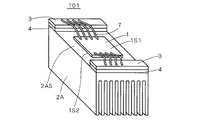
図34に第1の従来のパワーモジュール101Pの模式的な外観図を示す。パワーモジュール101Pでは、放熱フィンないしはヒートシンク2P上に熱伝導グリス(図示せず)を介して銅ベース板9Pが配置されており、ベース板9P上に絶縁基板5Pが配置されている。更に、絶縁基板5P上にフリーホイーリングダイオード(以下、単にダイオードとも呼ぶ)1AP及び絶縁ゲート型バイポーラトランジスタ(Insulated Gate Bipolar Transistor;以下、IGBTとも呼ぶ)1BPが配置されている。
【0003】
従来のパワーモジュール101Pでは、絶縁基板5Pの両主面には銅箔6Pが形成されており、銅箔6Pとベース板9Pとが半田付けされており、又、ダイオード1AP及びIGBT1BPは銅箔6P上に半田付けされている。更に、ヒートシンク2P上に絶縁層4Pを介して電極3Pが設けられている。そして、ワイヤ7Pによって所定の電気的結線がなされている。なお、ヒートシンク2P,ダイオード1AP及びIGBT1BP等を含む構成はケース(図示せず)内に収められている。
【0004】
電極3Pにバスバーないしは配線91Pが接続されており、バスバー91Pは上記ケースの外に引き出されている。ケースの外においてバスバー91Pに電流検出用の変流器ないしはカレント・トランスフォーマ92Pが取り付けられている。また、円筒形の直流電流平滑用キャパシタ8Pが、ケースの外にヒートシンク2P等とは別個に設けられている(その接続形態の図示化は省略する)。
【0005】
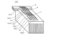
図35に第2の従来のパワーモジュール102Pの模式的な外観図を示す。パワーモジュール102Pは上述のベース板9Pを有さず、絶縁基板5Pが熱伝導グリスを介してヒートシンク2P上に配置されている。パワーモジュール102Pのその他の構造は上述のパワーモジュール101Pと同様である。
【0006】
図36に第3の従来のパワーモジュール103Pの模式的な外観図を示す。パワーモジュール103Pは、いわゆる電力変換器である。パワーモジュール103Pでは、全てのダイオード1AP及びIGBT1BPが絶縁基板5P上に配置されている。なお、パワーモジュール103Pのヒートシンク2BPは貫通孔2BHPを有しており、かかる貫通孔2BHPに冷媒が流される。パワーモジュール103Pのその他の構造は基本的には上述のパワーモジュール101Pと同様である。
【0007】
【発明が解決しようとする課題】
従来のパワーモジュール101P〜103Pは以下の問題点を有している。まず、動作時の温度に対する信頼性が低いという問題点がある。
【0008】
詳細には、ヒートシンク2P,2BPとダイオード1AP及びIGBT1BPとの熱膨張率が異なる場合、上述の半田付け部分では半田の凝固点からの温度差に応じた熱応力が発生する。このため、パワーモジュール101P〜103Pの使用時(動作時)における熱サイクル(又は温度サイクル)及び/又は使用と停止との繰り返しによる熱サイクルによって半田付け部分に亀裂が発生・進行するという問題点がある。このような半田付け部分の亀裂はパワーモジュールの寿命を縮めてしまう。
【0009】
このとき、上述の熱応力を小さくするためには例えば半田を厚く(例えば300μm以上)することが考えられる。ところが、そのような厚さではダイオード1AP等とヒートシンク2P,2BPとの間の熱抵抗が大きくなってしまい、ヒートシンク2P,2BPを大型化しなければならないという別個の問題が惹起される。
【0010】
更に、従来のパワーモジュール101P〜103Pでは、ダイオード1AP等の発熱によって絶縁基板5Pやベース板9P等に温度分布が生じると絶縁基板5P等に反りやうねりが発生する。このとき、温度差が大きい場合には、ヒートシンク2Pとベース板9Pとの間等に隙間が形成される。このため、ヒートシンク2P,2BPと絶縁基板5P又はベース板9Pとの間が熱伝導グリスで満たされなくなり(空気が入り込み)、熱伝達が低下してしまうという問題点がある。また、上述の半田付け部分の亀裂の発生が助長される又は亀裂が進行するという問題点がある。かかる隙間が形成されると、パワーモジュールの信頼性が低下してしまう。
【0011】
上述の隙間を発生させないようにするためには、例えば絶縁基板5P等内での温度分布を均一化したり、絶縁基板5P等を厚くして剛性を増大させることが考えられる。しかしながら、絶縁基板5P等を厚くすると絶縁基板5P等とヒートシンク2P,2BPとの間の熱抵抗が大きくなってしまい、かかる場合にもヒートシンク2P,2BPを大型化しなければならないという別個の問題が惹起される。
【0012】
更に、ダイオード1APやIGBT1BPの発熱量が大きい場合、温度上昇によって素子の特性が変動してしまうので、信頼性を確保するためには電流量を制限しなければならないという問題点がある。
【0013】
更に、従来のパワーモジュール101P〜103Pでは、変流器92P及び円筒形のキャパシタ8Pをパワーモジュールのケースの外に別個に設けているので、モジュール全体が大型であるという問題点がある。また、変流器92Pの特性は、測定する電流が直流成分を多く含む場合には大型化してしまうし、変流器92Pによれば発熱による特性変動に起因した測定誤差(5%程度)を含んで測定が行われてしまう。
【0014】
また、パワーモジュール103Pでは、ダイオード1AP及びIGBT1BPの各電力用半導体素子の配置位置によって、各電力用半導体素子と、電力変換器において低電位側に接続される電極61P及び高電位側に接続される電極62Pとの距離が異なっている。このため、ワイヤ7P等の配線のインダクタンスが電力用半導体素子毎に異なり、その結果、出力電圧がばらついてしまう。
【0015】
本発明はかかる問題点に鑑みてなされたものであり、小型軽量で信頼性の高いパワーモジュールを提供することを主たる目的とする。
【0016】
【課題を解決するための手段】
(1)請求項1に記載の発明に係るパワーモジュールは、ヒートシンクと、前記ヒートシンク上に直に配置された第1の電力用半導体素子と、前記ヒートシンク上に直に配置されたキャパシタとを備え、前記ヒートシンクは導電性を有し、前記第1の電力用半導体素子の電極及び前記キャパシタの電極が前記ヒートシンクと直に接着されていることを特徴とする。
【0017】
(2)請求項2に記載の発明に係るパワーモジュールは、請求項1に記載のパワーモジュールであって、前記ヒートシンクは複数の表面を有し、前記第1の電力用半導体素子と前記キャパシタとが前記ヒートシンクの異なる前記表面上に配置されていることを特徴とする。
【0018】
(3)請求項3に記載の発明に係るパワーモジュールは、請求項1又は2に記載のパワーモジュールであって、前記ヒートシンクは冷媒の流路を有することを特徴とする。
【0020】
(4)請求項4に記載の発明に係るパワーモジュールは、請求項1乃至3のいずれかに記載のパワーモジュールであって、前記ヒートシンク上に配置された絶縁基板と、前記絶縁基板を介して前記ヒートシンク上に配置された第2の電力用半導体素子とを更に備えることを特徴とする。
【0021】
(5)請求項5に記載の発明に係るパワーモジュールは、請求項1乃至3のいずれかに記載のパワーモジュールと、他のヒートシンクと、前記他のヒートシンク上に直に配置された第2の電力用半導体素子とを備えることを特徴とする。
【0022】
(6)請求項6に記載の発明に係るパワーモジュールは、請求項5に記載のパワーモジュールであって、前記他のヒートシンクは導電性を有し、前記他のヒートシンクに、前記第2の電力用半導体素子の電極が直に接着されており、前記パワーモジュールは、前記他のヒートシンクを前記ヒートシンク及び前記キャパシタの前記電極から絶縁する絶縁部材を更に備えることを特徴とする。
【0023】
(7)請求項7に記載の発明に係るパワーモジュールは、請求項6に記載のパワーモジュールであって、前記絶縁部材上に配置された導電部材と、前記導電部材に接続されると共に、前記第1の電力用半導体素子と前記第2の電力用半導体素子との間を電気的に接続する可撓性の配線とを更に備えることを特徴とする。
【0027】
(8)請求項8に記載の発明に係るパワーモジュールは、請求項4乃至7のいずれかに記載のパワーモジュールであって、前記第1の電力用半導体素子と前記第2の電力用半導体素子とは電気的に接続されて、前記第1の電力用半導体素子は電力変換器の下アームを成し、前記第2の電力用半導体素子は前記電力変換器の上アームを成すことを特徴とする。
【0028】
(9)請求項9に記載の発明に係るパワーモジュールは、請求項8に記載のパワーモジュールであって、前記上アーム及び前記下アームを含む、前記電力変換器のアームの複数と、各前記下アームの各前記第1の電力用半導体素子に第1電圧を供給する第1電極及び各前記上アームの各前記第2の電力用半導体素子に第2電圧を供給する第2電極を含み、前記第1の電力用半導体素子又は前記第2の電力用半導体素子の配置面から突出して設けられた同軸線とを更に備え、複数の前記アームは、前記同軸線を取り囲んで同心円上に略等間隔で配置されていることを特徴とする。
【0031】
【発明の実施の形態】
<実施の形態1>
図1に実施の形態1に係るパワーモジュール101の模式的な外観図を示す。
図1に示すように、パワーモジュール101は、例えばシリコン(Si)基板に形成された電力用半導体素子(例えばフリーホイーリングダイオードやIGBT)1と、ヒートシンク2Aと、電極3と、絶縁層4と、ワイヤ7とを備える。なお、図面の煩雑化を避けるため、電力用半導体素子1の詳細な図示化は省略している。
【0032】
特に、電力用半導体素子1はヒートシンク2A上に直に配置されているないしは接している。電力用半導体素子1は、上記シリコン基板の両主面に対応する両主面1S1,1S2を有しており、各主面1S1,1S2にそれぞれ電極(図示せず)が形成されている。そして、一方の主面(以下、裏面とも呼ぶ)1S2が、換言すれば当該裏面1S2に形成された電極(以下、裏面電極とも呼ぶ)がヒートシンク2Aの平面状の表面2AS上に例えば半田付けされている。
【0033】
ここで、「電力用半導体素子1がヒートシンク2A上に直に配置されている」とは、「従来のパワーモジュール101P〜103Pが有する絶縁基板5Pやベース板9P(図34参照)を介することなく」の意味であり、電力用半導体素子1とヒートシンク2Aとの間に両者を接着するための接着材料(例えば上述の半田)が存在している構成は上述の「直に配置」された形態に含まれる。なお、上記接着材料として、半田の代わりに、アルミニウムや銀等の導電性粉末を含んだエポキシ樹脂等の熱伝導性の良好な接着剤を用いても構わない。
【0034】
ヒートシンク2Aはシリコンと熱膨張率がほぼ等しい材料、例えばモリブデン(Mo),銅(Cu)−モリブデン(Mo)合金,タングステン(W),炭素繊維複合材料等を含む。或いは、ヒートシンク2Aとして(シリコンと熱膨張率がほぼ等しい材料として)、炭素(C)やシリコン(Si)を含有したアルミニウム(Al)等を適用する。ヒートシンク2Aは表面2ASの反対側にフィン形状を有している。
【0035】
更に、ヒートシンク2A上に絶縁層4が配置されており、絶縁層4上に電極3が配置されている。即ち、電極3は絶縁層4により絶縁されてヒートシンク2A上に配置されている。電極3と、電力用半導体素子1の他方の主面(以下、表面とも呼ぶ)1S1に形成された電極(以下、表面電極とも呼ぶ)とがワイヤ7によって電気的に結線されている。なお、圧接や導電性接着剤等によって、電極3と電力用半導体素子1の表面電極とを電気的に接続しても構わない。
【0036】
パワーモジュール101によれば以下の効果を得ることができる。即ち、電力用半導体素子1とヒートシンク2Aとの熱膨張率がほぼ等しいので、従来のパワーモジュール101P〜103Pとは異なり、電力用半導体素子1とヒートシンク2Aとの接合部分(半田付け部分)に熱サイクルに起因した亀裂が発生するのを格段に抑制することができる。このため、従来のパワーモジュール101P〜103Pとは異なり、半田を厚くする必要が無く、電力用半導体素子1とヒートシンク2Aとの間の熱抵抗を小さくすることができる。これにより、ヒートシンクを小型軽量化することができる。
【0037】
更に、電力用半導体素子1とヒートシンク2Aとが直に接しているので、電力用半導体素子1とヒートシンク2Aとの間の温度差を小さくすることができる。このため、従来のパワーモジュール101P〜103Pとは異なり、たとえ電力用半導体素子1の裏面1S2内に及び/又はヒートシンク2Aの表面2AS内に温度分布が生じた場合であっても、裏面1S2と表面2ASとの間に発生する或いは裏面1S2と表面2ASとの間の接着材料に発生する熱応力が小さい。これにより、電力用半導体素子の信頼性を高められ、パワーモジュール101によれば高い信頼性を長期に得ることができる。
【0038】
<実施の形態2>
図2に実施の形態2に係るパワーモジュール102の模式的な外観図を示す。図2に示すように、パワーモジュール102は、既述の電力用半導体素子1としてのフリーホイーリングダイオード1A及びIGBT1Bと、ヒートシンク2Aと、電極3と、絶縁層4と、ワイヤ7とを備える。なお、既述の構成要素と同等のものには同一の符号を付してその説明を援用するに留める。
【0039】
フリーホイーリングダイオード1Aは、既述の各表面1S1及び裏面1S2に対応する表面1AS1及び裏面1AS2と、表面電極及び裏面電極(図示せず)とを有する。同様に、IGBT1Bも、既述の各表面1S1及び裏面1S2に対応する表面1BS1及び裏面1BS2と、表面電極及び裏面電極(図示せず)とを有する。
【0040】
特に、パワーモジュール102のヒートシンク2Aは導電性を有する材料、例えば上述の材料の内の銅−モリブデン合金等から成る。そして、ダイオード1A及びIGBT1Bが、裏面1AS2,1BS2をヒートシンク2Aの表面2ASに対面させて、ヒートシンク2A上に直に配置されている。ダイオード1A及びIGBT1Bは、導電性を有する接着材料、例えば半田でヒートシンク2A上に接着されている。これにより、ダイオード1A及びIGBT1Bの両裏面電極は半田及び導電性のヒートシンク2Aを介して電気的に接続されている。他方、ダイオード1Aの表面電極とIGBT1Bの表面電極と電極3とが例えばワイヤ7によって電気的に接続されている。
【0041】
このように、パワーモジュール102では、ヒートシンク2Aが導電性を有するので、即ちヒートシンク2Aが電極として働くので、電極3及び絶縁層4の個数を削減してパワーモジュールを小型軽量化することができる。
【0042】
なお、パワーモジュール102のヒートシンク2Aは、表面2ASから続く突出部2ATを有しており、絶縁層4及び電極3は突出部2AT上にも延在している。これにより、導電性のヒートシンク2Aの突出部2ATと突出部2AT上の電極3とをパワーモジュール102の端子として利用することができる。
【0043】
なお、パワーモジュール102は主として複数の電力用半導体素子の各裏面電極が同一電位となる回路構成に適用されるが、ヒートシンク2Aと電力用半導体素子との間に、銅箔等の導電層を有する絶縁基板(従来の絶縁基板5P(図34参照)に相当)を設けることによって、裏面電極の電位が異なる複数の電力用半導体素子を搭載することができる。
【0044】
<実施の形態3>
図3に実施の形態3に係るパワーモジュール103の模式的な外観図を示す。図3に示すように、パワーモジュール103は、2つのパワーモジュール102が絶縁部材10を介して結合され一体化された構成を有する。絶縁部材10として例えばエポキシ樹脂や射出成形プラスチック等が適用可能である。
【0045】
パワーモジュール103では、各パワーモジュール102の電極3は、互いに他方のパワーモジュール102側へ延在して当該他方のパワーモジュール102のヒートシンク2Aに電気的に接続されている、例えば半田付けされている(突出部3T参照)。
【0046】
パワーモジュール103によれば、2つのパワーモジュール102を予め準備しておき、これらを組み合わせて回路を構成するので、モジュールを容易に形成することができる。このとき、小型軽量化が推進されたパワーモジュール102を用いるので、パワーモジュール103も小型軽量化される。なお、3つ以上のパワーモジュール102を組み合わせても構わない。
【0047】
なお、電極3を介することなく、例えばダイオード1Aとヒートシンク2Aとの間を直接にワイヤ7で接続しても構わない。かかる場合には、電極3等を更に削減することができる。
【0048】
<実施の形態4>
図4に実施の形態4に係るパワーモジュール104の模式的な外観図を示す。図4に示すように、パワーモジュール104は、フリーホイーリングダイオード1Aと、IGBT1Bと、導電性のヒートシンク2Bと、電極3と、絶縁層4と、ワイヤ7とを備える。
【0049】
ヒートシンク2Bは上述の導電性のヒートシンク2Aと同様の材料から成り、上記表面2ASに対応する平面状の表面2BSを有する。そして、当該表面2BS上にダイオード1A,IGBT1B及び絶縁層4が配置されている。
【0050】
特に、パワーモジュール104のヒートシンク2Bは冷媒の流路としての2つの貫通孔(冷媒の流路)2BHを有する。各貫通孔2BHは表面2BSから同程度離れた位置に、換言すれば図4において横方向に並べて設けられている。また、各貫通孔2BHはダイオード1A及びIGBT1Bの下方を通過するように形成されている。なお、貫通孔2BHは1つ或いは3つ以上であっても構わない。
【0051】
パワーモジュール104では、貫通孔2BHに冷媒、例えば空気,六フッ化硫黄(SF6),炭酸ガス等の気体や、水,油等の液体を流すことによって、ヒートシンク2Bを従ってダイオード1A及びIGBT1Bを強制的に冷却する。これにより、冷却能力を大幅に向上させることができる。その結果、従来のパワーモジュール101P〜103Pのように信頼性を確保するためになされていた電流量の制限を緩和或いは解除することができるし、又、ヒートシンクを、従ってパワーモジュールを小型軽量化することができる。
【0052】
<実施の形態4の変形例1>
図5に実施の形態4の変形例1に係るパワーモジュール104Aの模式的な外観図を示す。図5に示すように、パワーモジュール104Aは上述のパワーモジュール104を2つ備え、ヒートシンク2Bの貫通孔2BH同士が配管2BJで繋がれて、両パワーモジュール104が連結している。
【0053】
このとき、(i)両ヒートシンク2Bを同電位に設定する場合、換言すれば両ヒートシンク2B上のダイオード1A等の裏面電極同士を同電位に設定する場合には、配管2BJと冷媒との少なくとも一方に導電性の材料・物質を用い(以下、導電連結と呼ぶ)、(ii)逆に、両ヒートシンク2B間を絶縁する場合には、換言すれば両ヒートシンク2B上のダイオード1A等同士を絶縁する場合には、配管2BJ及び冷媒の双方に絶縁性の材料・物質を用いる(以下、絶縁連結と呼ぶ)。
【0054】
このとき、(iii)上記(i)のように配管2BJと冷媒との少なくとも一方に導電性の材料・物質を用いた場合であっても、ヒートシンク2Bとダイオード1A等との間に既述の絶縁基板5P(及び銅箔6P)(図34参照)を設ければ、上記(ii)と同様に両ヒートシンク2B間でダイオード1A等を絶縁することができる。逆に言えば、上述の導電連結及び絶縁連結によれば、絶縁基板5P等を用いる必要がない。
【0055】
なお、3つ以上のパワーモジュール104を配管2BJで連結してパワーモジュール104Aを構成しても良い。このとき、導電連結の場合、同電位に設定する複数のパワーモジュール104を1グループとして、各グループ毎に、冷媒を流すためのポンプ(図示せず)を設ける。他方、絶縁連結の場合、パワーモジュール104A全体に対して、1つのポンプを設ければ良い。
【0056】
<実施の形態4の変形例2>
図6に実施の形態4の変形例2に係るパワーモジュール104Bの模式的な外観図を示す。図6に示すように、パワーモジュール104Bでは、2つの貫通孔2BHが表面2BSからの距離を違えて、換言すれば図6において上下に並べて形成されている。
【0057】
上述のパワーモジュール104Aと同様に、複数のパワーモジュール104Bの各貫通孔2BH同士を配管2BJで連結して回路を構成しても構わない(図7参照)。このとき、上側の貫通孔2BH同士を及び下側の貫通孔2BH同士をそれぞれ配管2BJでつなぐ。特に、ダイオード1A及びIGBT1Bに近い、上側の貫通孔2BHから冷媒を流入し、その後、折り返して下側の貫通孔2BHに流れるように配管することによって、上記パワーモジュール104と比較して、各ヒートシンク2Bでの冷媒の温度差が吸収され、より均一な冷却能力が得られる。
【0058】
<実施の形態4の変形例3>
図8に実施の形態4の変形例3に係るパワーモジュール104Cの模式的な外観図を示す。図8に示すように、パワーモジュール104Cは上記パワーモジュール104を2つ備え、両パワーモジュール104がヒートシンク2Bの表面2BSとは反対側の表面同士を接して配置されている。
【0059】
<実施の形態4の変形例4>
図9に実施の形態4の変形例4に係るパワーモジュール104Dの模式的な外観図を示す。図9に示すように、パワーモジュール104Dは上記パワーモジュール104を2つ備え、両パワーモジュール104が支持部材15を介して上下に積み重ねられている。このとき、(i)少なくとも1つの支持部材15に金属等の導電性部材を用いれば両ヒートシンク2Bを同電位に設定することができるし、(ii)全ての支持部材15に樹脂等の絶縁部材を用いれば両ヒートシンク2B間を絶縁することができる。
【0060】
<実施の形態5>
図10及び図11に、実施の形態5に係るパワーモジュール105の模式的な外観図(上面図及び側面図)を示す。なお、図11は図10中の矢印Aの方向からパワーモジュール105を見た場合の外観図にあたり、図面の煩雑化を避けるために図11では構成要素の一部の図示化を省略している。また、図12に、パワーモジュール105の模式的な縦断面図を示す。
【0061】
パワーモジュール105は、いわゆる3相の電圧型電力変換器を成す。なお、電力変換器とはインバータ及びコンバータを含む。電力変換器では、各相毎に、互いに対を成してアームを形成する上アームと下アームとが出力端子を介して直列に接続され、上アームは高電位(第2電圧に対応する)側と出力端子との間に接続され、下アームは出力端子と低電位(第1電圧に対応する)側との間に接続される(又は接地される)。即ち、電力変換器は、等価回路的には多相ブリッジ回路(ここでは、3相ブリッジ回路)を成している。
【0062】
パワーモジュール105は、対向する円形の主面(表面)2CS1,2CS2を有する円柱形のヒートシンク2Cを備える。ヒートシンク2Cは導電性を有する。
【0063】
ヒートシンク2Cの一方の主面2CS1上に例えばセラミック板より成る3つの絶縁基板50U,50V,50Wが配置されている。各絶縁基板50U,50V,50Wの両主面上に例えば銅箔が形成されており、絶縁基板50U,50V,50Wは例えば半田により主面2CS1上に接着されている。このとき、ヒートシンク2Cと対面する上記銅箔は、絶縁基板50U,50V,50Wとヒートシンク2Cとの間の接着を良好に行うためのものである。他方、各絶縁基板50U,50V,50W上の、ヒートシンク2Cとは対面しない各銅箔は、電力変換器の出力端子にあたる各電極60U,60V,60Wを成す。このため、電極60U,60V,60Wとして銅箔以外の導電材料を用いても構わない。
【0064】
特に、絶縁基板50U,50V,50Wは、円形の主面2CS1の円周と同心の円周上に略等間隔に配置されている。換言すれば、円形の主面2CS1の中心に対して互いに同じ角度(ここでは120゜)を成して規定される放射線上に上記中心から同じ距離だけ離れて、絶縁基板50U,50V,50Wが配置されている。
【0065】
更に、各1つのダイオード1A及びIGBT1Bから成る電力用半導体素子の組が、3組、絶縁基板50U,50V,50Wに隣接して主面2CS1上に直に配置されている。上述の電力用半導体素子の各組は、円形の主面2CS1の円周と同心の円周上に略等間隔に又上記各絶縁基板50U,50V,50Wの配列間に配置されている。特に、かかるダイオード1A及びIGBT1Bの各裏面電極は例えば半田により主面2CS1上に直に接着されている。他方、ダイオード1A及びIGBT1Bの各表面電極は例えばワイヤ7により電極60U,60V,60Wに電気的に接続されている。このようにヒートシンク2C上に直付けされている、3組のダイオード1A及びIGBT1Bの各組が電力変換器の下アームを構成する。
【0066】
更に、例えばセラミック板より成る絶縁基板5が絶縁基板50U,50V,50Wに近接して主面2CS1上に配置されている。各絶縁基板5は、円形の主面2CS1の円周と同心の円周上に略等間隔に又上記各絶縁基板50U,50V,50Wの配列間に配置されている。各絶縁基板5の両主面上に例えば銅箔が形成されており、各絶縁基板5は例えば半田により主面2CS1に接着されている。ヒートシンク2Cと対面しない側の銅箔は導電層6を成す。
【0067】
各絶縁基板5の導電層6上にダイオード1A及びIGBT1Bが配置されている。ダイオード1A及びIGBT1Bはそれぞれの裏面電極を導電層6と対面させて例えば半田により接着されている。また、隣接する導電層6と電極60U,60V,60Wとが例えばワイヤ7によって接続されている。絶縁基板5を介してヒートシンク2C上に配置されている、3組のダイオード1A及びIGBT1Bそれぞれが電力変換器の上アームを構成する。
【0068】
ダイオード1A等のかかる配置によれば、パワーモジュール105が有する3つのアーム(上アーム及び下アームから成る)は、ヒートシンク2Cの円形の主面2CS1の当該円形の中心(後述のように電極61が配置される)を取り囲んで同心円上に略等間隔で配置されている。
【0069】
そして、円形の主面2CS1上に、当該円形の中心付近に例えばセラミック板より成る絶縁基板50Cが配置されている。絶縁基板50Cの両主面上には例えば例えば銅箔が形成されており、絶縁基板50Cは例えば半田により主面2CS1に接着されている。ヒートシンク2Cと対面しない銅箔は導電層60Cを成す。絶縁基板5上のダイオード1A及びIGBT1Bの各表面電極が例えばワイヤ7により導電層60Cと電気的に接続されている。なお、絶縁基板50Cや導電層60C等の形状は、図10等に図示された形状に限られない。
【0070】
特に、ダイオード1A等の設置面である円形の主面2CS1の略中心から絶縁基板50Cを貫いて例えば棒状の電極61が伸びている(図12参照)。電極61はヒートシンク2Cと電気的に接続されている。また、導電層60Cと電気的に接続されて電極62が配置されている。電極62は例えば筒状の電極から成り、その筒状の内部に電極61が挿入されている。電極61,62間には絶縁部材11が配置されており、両電極61,62は絶縁されている。電極61,62はいわゆる同軸線を成す。なお、パワーモジュール105では、電極61が「第1電極」にあたり、電極62が「第2電極」にあたる。
【0071】
このような構成により、パワーモジュール105は、5つの電極60U,60V,60W,61,62を有する電力変換器を成している。
【0072】
ここで、図13にヒートシンク2Cが有する貫通孔2CHを説明するための模式図を示す。なお、図13は図10に相当する図面であり、図面の煩雑化を避けるために図10中の絶縁基板5等の図示化は省略している。図13に示すように、ヒートシンク2Cには、主面2CS1の円周と同心の略リング状の貫通孔2CHが3つ形成されている(それぞれを各種破線で示す)。各貫通孔2CHに冷媒を流すことにより、パワーモジュール105の冷却を行う。貫通孔2CHの個数は3つに限られないが、貫通孔2CHを発熱体であるダイオード1A及びIGBT1Bの下方に設けることが好ましい。また、貫通孔2CHをリング状でなく例えば渦巻き状に設けても構わない。また、パワーモジュール104B(図6参照)のように、主面2CS1,2CS2間に上下に重ねて貫通孔2CHを設けても構わない。
【0073】
パワーモジュール105によれば、上述のように電力変換器の3つのアームは上記同軸線を取り囲んで同心円上に略等間隔で配置されている。このため、電極61,62と各アームとの間の配線を同様に形成することができるので、各アームから取り出される各出力のばらつきを小さくすることができると共に、低電位側の変動を小さくできるため誤動作に強くすることができる。その結果、信頼性の高い電力変換器を提供することができる。
【0074】
<実施の形態5の変形例1>
なお、パワーモジュール105ではヒートシンク2Cの主面2CS1上にダイオード1A等を全て配置したが、その一部をシートシンク2Cの他方の主面2CS2上に配置しても構わない。例えば、3つの絶縁基板5及びそれの上に配置された構成要素を主面2CS2上に配置し、所定の配線を行っても構わない。
【0075】
<実施の形態6>
図14に実施の形態6に係るパワーモジュール111の模式的な外観図を示す。図14に示すように、パワーモジュール111では、貫通孔2BHを有する既述の導電性のヒートシンク2Bの表面2BS上に、ダイオード1A,IGBT1B及び直流電流平滑用のコンデンサないしはキャパシタ20が直に配置されている。なお、ダイオード1A及びIGBT1Bがそれぞれ「第1の電力用半導体素子」にあたる。
【0076】
既述のように、ダイオード1Aはシリコン基板の両主面に対応する両主面(表面1AS1及び裏面1AS2)を有しており、表面1AS1に表面電極が又裏面1AS2に裏面電極が形成されている。同様に、IGBT1Bにおいても、表面1BS1に表面電極が又裏面1BS2に裏面電極が形成されている。なお、図面の煩雑化を避けるため、図14ではダイオード1A及びIGBT1Bそれぞれの表面電極及び裏面電極の詳細な図示化は省略している。
【0077】
特に、従来の円筒形のキャパシタ8Pとは異なり、キャパシタ20は、対向する2つの主面20S1,20S2を有する平板形のキャパシタから成る。そして、平板形の一方の主面(以下、裏面とも呼ぶ)20S2に電極(図示せず;裏面電極とも呼ぶ)が形成されており、他方の主面(以下、表面とも呼ぶ)20S1に電極(図示せず;表面電極とも呼ぶ)が形成されている。
【0078】
ダイオード1A,IGBT1B及びキャパシタ20の各裏面電極はヒートシンク2Bに例えば半田により接着されている。これにより、各裏面電極同士が導電性のヒートシンク2Bを介して電気的に接続されている。他方、ダイオード1A,IGBT1B及びキャパシタ20の各表面電極(ヒートシンク2Bとは対面していない)同士はワイヤ7によって結線されている。なお、圧接や導電性接着剤等によって、各表面電極間を電気的に接続しても構わない。
【0079】
パワーモジュール111によれば以下の効果を得ることができる。まず、小型軽量で信頼性の高いパワーモジュール111を提供することができる。
【0080】
詳細には、ダイオード1A及びIGBT1B及びキャパシタ20がヒートシンク2B上に直付けされている。このため、これらが別々に設けられている従来のパワーモジュール101P〜103Pよりも、パワーモジュールを小型化することができる。また、ヒートシンク2Cの放熱作用によってダイオード1A及びIGBT1Bの発熱のみならずキャパシタ20の温度上昇をも抑制することができるため、キャパシタ20の小型化、低インダクタンス化、長寿命化が図れる。
【0081】
更に、ダイオード1A,IGBT1B及びキャパシタ20がヒートシンク2B上に直付けされているので、ダイオード1A及びIGBT1Bとキャパシタ20との間を結ぶ配線の長さを従来のパワーモジュール101P〜103Pよりも短くすることができる。特に、ヒートシンク2Bは導電性を有するので、ダイオード1A,IGBT1B及びキャパシタ20はヒートシンク2Bを介して最短経路で電気的に結ばれている。このため、従来のパワーモジュール101P〜103Pよりも回路インダクタンスを低減することができる。従って、ダイオード1A及びIGBT1Bのスイッチング動作時に生じる跳ね上がり電圧(オーバーシュート)を低減でき、その結果、ダイオード1A及びIGBT1Bの耐圧及び損失を低減することができる。また、配線長が短くなることに起因して、電磁ノイズの発生を低減することができる。
【0082】
また、パワーモジュール111によれば、ヒートシンク2Bが導電性を有するので、当該ヒートシンク2Bを電極として用いることができる。このため、例えば、絶縁性のヒートシンクの場合に必要な配線等の部品点数及びそれの形成工程を削減することができる。
【0083】
なお、ヒートシンク2Bの貫通孔2BHに冷媒を流すことによって、ヒートシンク2Bの冷却能力を向上することができる。
【0084】
<実施の形態6の変形例1>
なお、ヒートシンク2Bに変えて、図15に示すパワーモジュール111Aのようにフィン構造を有する導電性のヒートシンク2Aを適用しても、上述の効果を得ることができる。
【0085】
<実施の形態6の変形例2>
また、キャパシタ20,ダイオード1A及びIGBT1Bを、ヒートシンク2Bの異なる表面に配置しても構わない。具体的には、図16に示すパワーモジュール111Bのように、ダイオード1A及びIGBT1Bをヒートシンク2Bの表面2BS上に配置する一方で、キャパシタ20を上記表面2BSと交わる他の表面(側面)2BS3上に配置しても構わない。また、上記表面2BSと対向する表面2BS2上に配置しても構わない。このような構成はヒートシンク2Aを用いる場合にも適用可能である。
【0086】
パワーモジュール111Bによれば、上記パワーモジュール111と比較して、パワーモジュールを更に小型軽量化することができる。また、ダイオード1A及びIGBT1Bの放熱とキャパシタ20の放熱との干渉が少なくなるので、放熱性を向上することができる。
【0087】
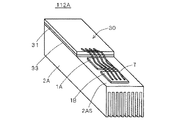
<実施の形態7>
図17に実施の形態7に係るパワーモジュール112の模式的な外観図を示す。図17と既述の図14とを比較すれば分かるように、パワーモジュール112は、キャパシタ20(図14参照)に変えて、キャパシタ用誘電体33及びキャパシタ用電極31を備える。詳細には、導電性のヒートシンク2Bとキャパシタ用電極31とでキャパシタ用誘電体33が挟み込まれており、ヒートシンク2Bとキャパシタ用誘電体33とキャパシタ用電極31とで以て上記キャパシタ20に相当する平板形のキャパシタ30が構成されている。その他の構成はパワーモジュール111と同様である。
【0088】
このとき、キャパシタ用電極31はキャパシタ20の表面電極にあたり、ヒートシンク2Bは同裏面電極にあたる。このため、パワーモジュール112では、ダイオード1A及びIGBT1Bがキャパシタ30の裏面電極上に配置されていると捉えることができる。
【0089】
パワーモジュール112によれば、上述のパワーモジュール111と同様の効果が得られる。
【0090】
<実施の形態7の変形例1>
なお、ヒートシンク2Bに変えて、図18に示すパワーモジュール112Aのようにフィン構造を有する導電性のヒートシンク2Aを適用しても構わない。
【0091】
<実施の形態7の変形例2>
図19に実施の形態7の変形例2に係るパワーモジュール112Bの模式的な外観図を示す。パワーモジュール112Bでは、パワーモジュール111B(図16参照)と同様に、キャパシタ用誘電体33及びキャパシタ用電極31が、表面2BSとは異なる、ヒートシンク2Bの表面2BS2上や表面2BS3上に配置されている。このような構成はヒートシンク2Aを用いる場合にも適用可能である。パワーモジュール112Bによれば、上述のパワーモジュール111Bと同様の効果が得られる。
【0092】
<実施の形態8>
図20に実施の形態8に係るパワーモジュール111Cの模式的な外観図を示す。パワーモジュール111Cは、いわゆる3相の電圧型電力変換器を成す。
【0093】
パワーモジュール111Cでは、キャパシタ20が、その裏面20S2をヒートシンク2Bの上記表面2BS2と対面させて、ヒートシンク2B上に直に配置されている。
【0094】
パワーモジュール111Cは電力変換器のアームを3つ備える。各アームの下アームを成す各1つのダイオード1A及びIGBT1Bは共に裏面電極をヒートシンク2Bに対面させてヒートシンク2Bの表面2BS上に直に配置されている。また、各下アームのダイオード1A及びIGBT1Bの各表面電極は、それぞれ電力変換器の出力端子を成す電極60U,60V,60Wに例えばワイヤ7によって電気的に接続されている。なお、各電極60U,60V,60Wは各絶縁基板(又は各絶縁層)50U,50V,50Wを介してヒートシンク2Bの表面2BS上に配置されている。
【0095】
他方、各アームの上アームを成す各1つのダイオード1A及びIGBT1B(それぞれが第2の電力用半導体素子にあたる)は、絶縁基板5を介してヒートシンク2Bの表面2BS上に配置されている。このとき、上アームのダイオード1A及びIGBT1Bの裏面電極は絶縁基板5上の導電層6と電気的に接続されている。各導電層6は各アーム用の電極60U,60V,60Wに例えばワイヤ7により電気的に接続されている。上アームを成すダイオード1A及びIGBT1Bの各表面電極は全てのアームに共通の電極61に例えばワイヤ7により電気的に接続される。
【0096】
電極61はヒートシンク2Bの表面2BSからキャパシタ20の表面20S1にまで延在してキャパシタ20の表面電極に電気的に接続されている。なお、電極61は絶縁層50によってキャパシタ20の表面電極以外の部分及びヒートシンク2Bと絶縁されている。
【0097】
なお、パワーモジュール111Cでは、電極61が、高電位側に接続される「第2電極」にあたり、ヒートシンク2Bが、低電位側に接続される「第1電極」にあたる。
【0098】
パワーモジュール111Cによれば、上アームのダイオード1A及びIGBT1Bは絶縁基板5を介してヒートシンク2B上に配置されている。このため、導電性のヒートシンク2B上に、裏面電極の電位が異なるダイオード1A及びIGBT1Bを混在させて回路を形成することができる。
【0099】
<実施の形態8の変形例1>
図21に実施の形態8の変形例1に係るパワーモジュール112Cの模式的な外観図を示す。上述のパワーモジュール111Cと同様に、パワーモジュール112Cは、いわゆる3相の電圧型電力変換器を成す。
【0100】
図21と既述の図20とを比較すれば分かるように、パワーモジュール112Cは、パワーモジュール111Cのキャパシタ20に変えて、キャパシタ用電極31及びキャパシタ用誘電体33を備える。詳細には、キャパシタ用誘電体33はヒートシンク2Bの表面2BS2と対面して配置され、ヒートシンク2Bとキャパシタ用電極31とで挟まれている。これにより、ヒートシンク2Bとキャパシタ用誘電体33とキャパシタ用電極31とで以て上述の平板形のキャパシタ30が構成されている。その他の構成はパワーモジュール111Cと同様である。
【0101】
パワーモジュール112Cによれば、ダイオード1A及びIGBT1Bがキャパシタ30の一方の電極上に配置されていると捉えられ、パワーモジュール112と同様の効果を得ることができる。また、上記パワーモジュール111Cと同様に、絶縁基板5によって裏面電極の電位が異なるダイオード1A及びIGBT1Bをキャパシタ30の電極上に混在させることができる。
【0102】
<実施の形態9>
図22及び図23に実施の形態9に係るパワーモジュール113の模式的な外観図を示す。図23は図22中の矢印Aの方向からパワーモジュール113を見た場合の外観図(側面図)に相当する。なお、図面の煩雑化を避けるため、図23では、ダイオード1A,IGBT1B及びワイヤ7の図示化を省略している。上述のパワーモジュール111Cと同様に、パワーモジュール113は、いわゆる3相の電圧型電力変換器を成す。
【0103】
図22と既述の図20とを比較すれば分かるように、パワーモジュール113では、電力変換器の全ての下アームのダイオード1A及びIGBT1Bが1つの下アーム用のヒートシンク2Bの表面2BS上に直に配置されている。そして、ヒートシンク2Bとキャパシタ20とが表面2BS2と裏面20S2とを対面させて配置されており、ヒートシンク2Bとキャパシタ20の裏面電極とが電気的に接している。
【0104】
他方、電力変換器の各上アームのダイオード1A及びIGBT1Bは各上アーム用の導電性を有するヒートシンク(他のヒートシンク)2B上に直に配置されており、パワーモジュール111C(図20参照)と同様に電極61と電気的に接続されている。各上アーム用の3つのヒートシンク2Bは互いに絶縁連結されている(図22では配管2BJの図示化は省略している)と共に、下アーム用のヒートシンク2B及びキャパシタ20の裏面電極とは絶縁部材10によって絶縁されている。なお、絶縁部材10で以て、4つのヒートシンク2Bとキャパシタ20とが一体的に結合している。
【0105】
各上アーム用のヒートシンク2Bは各アーム用の電極60U,60V,60Wと例えばワイヤ(可撓性の配線)7で電気的に接続されている。特に、当該ワイヤ7は、電極60U,60V,60Wの内で絶縁部材10上に配置された部分(導電部材)を中継点ないしは経由点として、上アームと下アームとを電気的に接続している。
【0106】
上述のように、パワーモジュール113では、絶縁部材10で以て、4つのヒートシンク2Bが互いに絶縁されている。このため、既述のパワーモジュール111C(図20参照)とは異なり、絶縁基板5を用いることなく、上アーム用のダイオード1A及びIGBT1Bの裏面電極と、下アーム用の同裏面電極との電位を違えることができる。このため、絶縁基板5の分だけ部品点数を削減できる。
【0107】
更に、パワーモジュール113では上アーム及び下アームの両構成が大略同等であるので、パワーモジュール全体の製造コストを低減することができる。その結果、安価なパワーモジュール113を提供することができる。
【0108】
また、上述のように上アームと下アームとを結線するワイヤ7は、電極60U,60V,60Wの内で絶縁部材10上に配置された部分(導電部材)に接続されている。このため、上記導電部材を介することなく直接に上アームと下アームとの間を接続する場合と比較して、当該配線の撓みないしは垂れを抑えることができる。その結果、配線の垂れによる短絡を防止することができる。
【0109】
<実施の形態10>
図24及び図25に実施の形態10に係るパワーモジュール111Dの模式的な外観図(側面図)及び縦断面図を示す。図24と既述の図11とを比較すれば分かるように、パワーモジュール111Dは基本的に既述のパワーモジュール105にキャパシタ20を設けた構成を有するので、パワーモジュール105と同様の構成については既述の説明を援用するに留め、パワーモジュール111Dの特徴部分を中心に説明を進める。なお、図24では図11と同様に構成要素の一部の図示化を省略している。
【0110】
なお、電力変換器の3つの下アームはそれぞれヒートシンク2Cに直付けされているダイオード1A及びIGBT1Bで構成され、電力変換器の3つの上アームはそれぞれ絶縁基板5を介してヒートシンク2C上に配置されているダイオード1A及びIGBT1Bで構成される。
【0111】
パワーモジュール111Dは、導電性のヒートシンク2Cの円形の主面2CS2上にキャパシタ20が直に配置されている。このとき、キャパシタ20はその裏面20S2をヒートシンク2Cに対面させて配置されており、キャパシタ20の裏面電極20E2(図25参照)とヒートシンク2Cとが電気的に接続されている。
【0112】
特に、パワーモジュール111Dでは電極61,62の接続形態が既述のパワーモジュール105とは異なる。詳細には、図25に示すように、棒状の電極61はヒートシンク2C及びキャパシタ20(表面電極20E1を除く)を貫いて延在し、キャパシタ20の表面電極20E1と電気的に接続されている。このとき、電極61と共に絶縁部材11も伸長されており、電極61がヒートシンク2C及びキャパシタ20(表面電極20E1を除く)から絶縁されている。他方、筒状の電極62は絶縁基板50Cを貫いて配置されており、ヒートシンク2Cと電気的に接続されている。
【0113】
パワーモジュール111Dでは、電極61が、電力変換器の高電位側に接続される「第2電極」にあたり、電極62が、低電位側に接続される「第1電極」にあたる。
【0114】
パワーモジュール111Dによれば、既述のパワーモジュール105と同様に、同軸線を取り囲む3つのアームの配置に起因して信頼性の高い電力変換器を提供することができると共に、従来のパワーモジュール103Pよりも小型軽量な電力変換器を提供することができる。
【0115】
<実施の形態10の変形例1>
図26及び図27に実施の形態10の変形例1に係るパワーモジュール112Dの模式的な外観図及び縦断面図を示す。上述のパワーモジュール111Dと同様に、パワーモジュール112Dは、いわゆる3相の電圧型電力変換器を成す。
【0116】
図26と既述の図24とを比較すれば分かるように、パワーモジュール112Dは、パワーモジュール111Dのキャパシタ20に変えて、キャパシタ用電極31及びキャパシタ用誘電体33を備える。詳細には、キャパシタ用誘電体33はヒートシンク2Cの主面2CS2と対面して配置され、ヒートシンク2Cとキャパシタ用電極31とで挟まれている。これにより、ヒートシンク2Cとキャパシタ用誘電体33とキャパシタ用電極31とで以て上述の平板形のキャパシタ30が構成されている。そして、パワーモジュール111Dと同様に、パワーモジュール112Dの棒状の電極61は、ヒートシンク2C,キャパシタ用誘電体33を貫いて延在し、キャパシタ用電極31と電気的に接続されている。その他の構成はパワーモジュール111Dと同様である。このため、パワーモジュール111Dと同様の効果を得ることができる。
【0117】
また、パワーモジュール112Dでは、ダイオード1A及びIGBT1Bがキャパシタ30の裏面電極上に配置されていると捉えられ、パワーモジュール112と同様の効果を得ることができる。
【0118】
<実施の形態11>
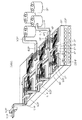
図28〜図30に実施の形態11に係るパワーモジュール111Eの模式図を示す。なお、パワーモジュール111Eは上述のパワーモジュール111Dを基本としているため、又、図面の煩雑化を避けるため、図28では一部のワイヤ7の図示化を省略し又図29及び図30では電極60U,60V,60W等の図示化を省略している。
【0119】
上述のモジュール111Dではダイオード1A及びIGBT1Bが全てヒートシンク2Cの一方の主面2CS1上に配置されているのに対して、パワーモジュール111Eではダイオード1A及びIGBT1Bがヒートシンク2Cの主面2CS1とキャパシタ20の表面20S1とに分散して配置されている。
【0120】
詳細には、導電性を有するヒートシンク2Cの主面2CS1上に、電力変換器の下アームを成すダイオード1A及びIGBT1Bが直に配置されている(図29参照)。そして、当該ダイオード1A及びIGBT1Bの表面電極同士が接続されている。他方、キャパシタ20の表面20S1上に(詳細には表面電極上に)、絶縁基板5が配置されており、絶縁基板5の導電層6上に、電力変換器の上アームを成すダイオード1A及びIGBT1Bが配置されている(図30参照)。絶縁基板5上のダイオード1A及びIGBT1Bの表面電極はキャパシタ20の表面20SIに接続されている。
【0121】
更に、上アームのIGBT1Bの裏面電極と導通する導電層6と下アームのIGBT1Bの表面電極とが接続されて電力変換器のアームを成す(配線7B参照)。3つのアームにおける上記接続点が電極60U,60V,60Wを成す。パワーモジュール111Eによっても、パワーモジュール111Dと同様の効果が得られる。
【0122】
なお、パワーモジュール111Eでは、ヒートシンク2Cが低電位側に接続され、キャパシタ20の表面電極が高電位側に接続される。このとき、図28〜図30への図示化は省略しているが、パワーモジュール111Dと同様の接続形態を有する同軸線(図25参照)によって給電しても構わず、かかる場合には電極62が「第1電極」にあたり、電極61が「第2電極」にあたる。
【0123】
また、上述のパワーモジュール111Dとパワーモジュール112Dとの関係のように、パワーモジュール111Eのキャパシタ20をキャパシタ用誘電体33及びキャパシタ用電極31に変更しても構わない。
【0124】
<実施の形態12>
図31に実施の形態12に係るパワーモジュール201の模式的な外観図を示す。パワーモジュール201は、2つの凹部(空間)202Kを有する絶縁性の筐体202を備える。筐体202の各凹部202K内には、ダイオード1Aが直付けされたヒートシンク2BとIGBT1Bが直付けされたヒートシンク2Bとが例えば交互に並べられて1列に収納されている。なお、図31ではダイオード1A及びIGBT1Bの結線の図示化は省略している。
【0125】
この際、各凹部202K内において各ヒートシンク2Bは隙間203を空けて並べられており、各隙間203間がヒートシンク2Bの貫通孔2BHで空間的に繋がれるように各ヒートシンク2B又は貫通孔2BHの向きが定められている。また、各凹部202Kの内面とヒートシンク2Bとの間に隙間203以外の隙間ができないように、ヒートシンク2B及び凹部202Kの寸法が規定されている。
【0126】
各凹部202Kにおいてヒートシンク2Bの並びの両端には隙間203が設けられており、各筐体202には当該各隙間203と繋がる穴が形成されている。そして、各凹部202Kの各一方の穴にはそれぞれ配管2BJが接続されており、各他方の穴は互いに配管2BJで繋がれて凹部202K同士が連結されている。
【0127】
隙間203には、筐体202の一部である絶縁性の蓋(図示せず)が被せられおり、これにより両凹部202Kがいわば一続きの空間を成す。このため、パワーモジュール201では、一方の凹部202Kの上記一方の穴から冷媒を流し込み、両凹部202K内に冷媒を流すことができる。このとき、筐体202及び上記蓋が共に絶縁性なので、例えば絶縁性の冷媒を用いれば各ヒートシンク2B間を絶縁することができる(絶縁連結)。なお、絶縁性の冷媒として、例えば空気,六フッ化硫黄(SF6)等の気体や、油等の液体が挙げられる。また、例えば導電性の冷媒を用いれば導電性のヒートシンク2B同士を同電位に設定可能である(導電連結)。また、絶縁性のヒートシンク2Bと導電性のヒートシンク2Bとを組み合わせ、導電性の冷媒を用いれば所望の導電性のヒートシンク2Bのみを導電連結することができる。
【0128】
さて、ダイオード1A及び/又はIGBT1Bを絶縁基板5を介してヒートシンク2B上に配置しても良く、かかる場合には導電性のヒートシンク2Bを用いた場合であっても所望のダイオード1A及び/又はIGBT1Bを他から絶縁することができる。逆に言えば、上述のようにヒートシンク2Bの導電性/絶縁性によって絶縁基板5を不要としうる。なお、1つのヒートシンク2B上に複数の電力用半導体素子を配置しても構わない。
【0129】
上述のように各ヒートシンク2Bは隙間203を空けて並べられているので、冷媒は隙間203と隙間203よりも狭い貫通孔2BHとを交互に通過する。このとき、冷媒が貫通孔2BHを通る時、換言すれば発熱体であるダイオード1A及びIGBT1Bの下方を通る時は、隙間203を通る時よりも、冷媒は速く流れる。これにより、冷却効果を増大させることができる。他方、隙間部203における冷媒の流れは貫通孔2BHにおけるそれよりも遅いので、圧力損失を抑えることができる。従って、パワーモジュール201によれば、より高い冷却性能をより低い圧力損失で以て実現することができる。
【0130】
また、上述のように、絶縁性の冷媒を用いることによって、絶縁基板5を用いることなく、換言すれば導電性のヒートシンク2B上にダイオード1A及び/又はIGBT1Bを直に配置する場合であっても、各電力用半導体素子を互いに絶縁することができる。このため、絶縁性の冷媒を用いることによって、絶縁基板5の分だけ部品点数を削減できる。更に、ダイオード1A及び/又はIGBT1Bを搭載した各ヒートシンク2Bはそれぞれ大略同等であるので、パワーモジュール全体の製造コスト及び価格を低減することができる。
【0131】
更に、上述の各電力用半導体素子が互いに絶縁されることに起因して、各電力用半導体素子を導電性のヒートシンク2B上に直に配置可能である。従って、パワーモジュールの放熱性能を向上することができ、その結果、信頼性を向上させることができる。
【0132】
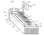
<実施の形態13>
図32に実施の形態13に係るパワーモジュール114の模式的な外観図を示す。図32に示すように、パワーモジュール114は、既述の図22に示すパワーモジュール113に対して電流測定用のシャント抵抗90を更に備える。詳細には、シャント抵抗90は電極60U,60V,60Wの出力端にそれぞれ直接、接続されており、各シャント抵抗90が電力変換器の各出力端子を成している。
【0133】
パワーモジュール114ではシャント抵抗90により電流を計測するので、従来のパワーモジュール101P等で用いられる変流器92Pとは異なり、制御電源が不要であるし、原理的にオフセットが無い。
【0134】
また、シャント抵抗90は電極60U,60V,60Wの出力端に直接に接続されているので、変流器92Pがケースの外に別個に設けられている従来のパワーモジュール101P等と比較して、パワーモジュール全体を小型軽量化することができるし、電流計測用部品の点数を削減することができる。
【0135】
<実施の形態13の変形例1>
図33に実施の形態13の変形例1に係るパワーモジュール114Aの模式的な外観図を示す。図33と上述の図32とを比較すれば分かるように、パワーモジュール114Aの各シャント抵抗90はヒートシンク2Bの表面2BSに対面する位置に設けられて各電極60U,60V,60Wと直接に接続されている。
【0136】
パワーモジュール114Aによれば、ヒートシンク2Bの作用によりシャント抵抗90の温度上昇を抑制することができる。このため、温度変化に起因したシャント抵抗の特性変化を大幅に抑制することができ、その結果、電流量の検出精度をさらに向上することができる。また、シャント抵抗90がヒートシンク2Bの上方に配置されているので、上述のパワーモジュール114と比較して更に小型化可能である。
【0137】
【発明の効果】
(1)請求項1に係る発明によれば、第1の電力用半導体素子及びキャパシタが共にヒートシンク上に直付けされている。このため、両者が別々に設けられている従来のパワーモジュールよりも、パワーモジュールを小型軽量化することができる。また、ヒートシンクの放熱作用によって第1の電力用半導体素子の発熱のみならずキャパシタの温度上昇をも抑制することができるため、キャパシタの小型化、低インダクタンス化、長寿命化が図れる。
【0138】
更に、第1の電力用半導体素子及びキャパシタが共にヒートシンク上に直付けされているので、両者の間を結ぶ配線の長さを上述の従来のパワーモジュールよりも短くすることができる。このため、回路インダクタンスを低減することができる。従って、第1の電力用半導体素子のスイッチング動作時に生じる跳ね上がり電圧(オーバーシュート)を低減でき、その結果、第1の電力用半導体素子の耐圧及び損失を低減することができる。また、配線長が短くなることに起因して、電磁ノイズの発生を低減することができる。
【0139】
従って、小型軽量で信頼性の高いパワーモジュールを提供することができる。
また、ヒートシンクは導電性を有するので、ヒートシンクを電極として用いることができる。このため、例えばヒートシンク上の配線等の部品点数及びそれの形成工程を削減することができる。
更に、第1の電力用半導体素子の電極及びキャパシタの電極がヒートシンクと直に接着されている。即ち、第1の電力用半導体素子とキャパシタとがヒートシンクを介して電気的に接続されている。このため、両電極間をワイヤ等の配線で接続する場合よりも更に両電極間の電気的接続を短くすることができる。その結果、回路インダクタンスの更なる低減により、上記跳ね上がり電圧(オーバーシュート)等を格段に低減することができる。
【0140】
(2)請求項2に係る発明によれば、第1の電力用半導体素子とキャパシタとはヒートシンクの異なる表面上に配置されているので、両者を同一表面上に配置する場合と比較して、パワーモジュールを更に小型軽量化することができる。また、第1の電力用半導体素子の放熱とキャパシタの放熱との干渉が少なくなるので、放熱性を向上することができる。
【0141】
(3)請求項3に係る発明によれば、ヒートシンクの流路に冷媒を流すことによって、ヒートシンクの冷却能力を更に向上することができる。
【0144】
(4)請求項4に係る発明によれば、第2の電力用半導体素子が絶縁基板を介してヒートシンク上に配置されている。このため、導電性のヒートシンク上に電位の異なる電力用半導体素子を配置して回路を構成することができる。
【0145】
(5)請求項5に係る発明によれば、他のヒートシンク上に配置された第2の電力用半導体素子を更に備える。このため、第1の電力用半導体素子と第2の電力用半導体素子とを組み合わせにより、回路を簡単に構成することができる。
【0146】
(6)請求項6に係る発明によれば、導電性の他のヒートシンクは、絶縁部材によって上記導電性のヒートシンク及びキャパシタの電極から絶縁されているので、絶縁基板を用いることなく、第1の電力用半導体素子と第2の電力用半導体素子との電位を違えることができる。このため、絶縁基板の分だけ部品点数を削減できる。更に、第1の電力用半導体素子及びヒートシンクを含む構成と、第2の電力用半導体素子及びヒートシンクを含む構成とは大略同等であるので、パワーモジュール全体の製造コストを低減することができる。その結果、安価なパワーモジュールを提供することができる。
【0147】
(7)請求項7に係る発明によれば、第1の電力用半導体素子と第2の電力用半導体素子とは、絶縁部材上に配置された導電部材を中継点とする可撓性の配線、例えばワイヤによって電気的に接続されている。このため、上記導電部材を介することなく直接に両電力用半導体素子間を可撓性の配線を電気的に接続する場合と比較して、当該配線の撓みないしは垂れを抑えることができる。その結果、配線の垂れによる短絡を防止することができる。
【0153】
(8)請求項8に係る発明によれば、信頼性の高い電力変換器を提供することができる。
【0154】
(9)請求項9に係る発明によれば、電力変換器の複数のアームは、同軸線を取り囲んで同心円上に略等間隔で配置されている。このため、第1電極及び第2電極と各アームとの間の配線を同様に形成することができるので、各アームから取り出される各出力のばらつきを小さくすることができると共に、第1電圧側の変動を小さくできるため誤動作に強くすることができる。
【図面の簡単な説明】
【図1】 実施の形態1に係るパワーモジュールの模式的な外観図である。
【図2】 実施の形態2に係るパワーモジュールの模式的な外観図である。
【図3】 実施の形態3に係るパワーモジュールの模式的な外観図である。
【図4】 実施の形態4に係るパワーモジュールの模式的な外観図である。
【図5】 実施の形態4の変形例1に係るパワーモジュールの模式的な外観図である。
【図6】 実施の形態4の変形例2に係るパワーモジュールの模式的な外観図である。
【図7】 実施の形態4の変形例2に係るパワーモジュールの模式的な外観図である。
【図8】 実施の形態4の変形例3に係るパワーモジュールの模式的な外観図である。
【図9】 実施の形態4の変形例4に係るパワーモジュールの模式的な外観図である。
【図10】 実施の形態5に係るパワーモジュールの模式的な外観図である。
【図11】 実施の形態5に係るパワーモジュールの模式的な外観図である。
【図12】 実施の形態5に係るパワーモジュールの模式的な縦断面図である。
【図13】 実施の形態5に係るパワーモジュールが有する貫通孔を説明するための模式図である。
【図14】 実施の形態6に係るパワーモジュールの模式的な外観図である。
【図15】 実施の形態6の変形例1に係るパワーモジュールの模式的な外観図である。
【図16】 実施の形態6の変形例2に係るパワーモジュールの模式的な外観図である。
【図17】 実施の形態7に係るパワーモジュールの模式的な外観図である。
【図18】 実施の形態7の変形例1に係るパワーモジュールの模式的な外観図である。
【図19】 実施の形態7の変形例2に係るパワーモジュールの模式的な外観図である。
【図20】 実施の形態8に係るパワーモジュールの模式的な外観図である。
【図21】 実施の形態8の変形例1に係るパワーモジュールの模式的な外観図である。
【図22】 実施の形態9に係るパワーモジュールの模式的な外観図である。
【図23】 実施の形態9に係るパワーモジュールの模式的な外観図である。
【図24】 実施の形態10に係るパワーモジュールの模式的な外観図である。
【図25】 実施の形態10に係るパワーモジュールの模式的な縦断面図である。
【図26】 実施の形態10の変形例1に係るパワーモジュールの模式的な外観図である。
【図27】 実施の形態10の変形例1に係るパワーモジュールの模式的な外観図である。
【図28】 実施の形態11に係るパワーモジュールの模式図である。
【図29】 実施の形態11に係るパワーモジュールの模式図である。
【図30】 実施の形態11に係るパワーモジュールの模式図である。
【図31】 実施の形態12に係るパワーモジュールの模式的な外観図である。
【図32】 実施の形態13に係るパワーモジュールの模式的な外観図である。
【図33】 実施の形態13の変形例1に係るパワーモジュールの模式的な外観図である。
【図34】 第1の従来のパワーモジュールの模式的な外観図である。
【図35】 第2の従来のパワーモジュールの模式的な外観図である。
【図36】 第3の従来のパワーモジュールの模式的な外観図である。
【符号の説明】
1 電力用半導体素子、1A フリーホイーリングダイオード(電力用半導体素子)、1B 絶縁ゲート型バイポーラトランジスタ(電力用半導体素子)、2A,2B,2C ヒートシンク、2AS,2BS,2BS2,2BS3 表面、2CS1,2CS2 主面(表面)、2BH 貫通孔(流路)、4 絶縁層、5,50C,50U,50V,50W 絶縁基板、60C 導電層、60U,60V,60W 電極(導電部材)、7 ワイヤ(可撓性の配線)、10 絶縁部材、20,30 キャパシタ、20E1,20E2 電極、31 キャパシタ用電極、33 キャパシタ用誘電体、50 絶縁層(絶縁部材)、61,62 電極、101〜105,104A〜104D,111〜114,111A〜111E,112A〜112D,114A,201 パワーモジュール、202 筐体、202K 凹部(空間)。[0001]
BACKGROUND OF THE INVENTION
The present invention relates to a power module, and mainly relates to a technique for improving the cooling performance of the power module.
[0002]
[Prior art]
FIG. 34 shows a schematic external view of the first
[0003]
In the
[0004]
A bus bar or
[0005]
FIG. 35 shows a schematic external view of a second
[0006]
FIG. 36 shows a schematic external view of a third
[0007]
[Problems to be solved by the invention]
The
[0008]
In detail, heat sink2P,When the thermal expansion coefficients of 2BP, the diode 1AP, and the IGBT 1BP are different, thermal stress corresponding to the temperature difference from the solidification point of the solder is generated in the soldering portion. For this reason, there is a problem that cracks occur and progress in the soldered part due to the thermal cycle (or temperature cycle) during use (operation) of the
[0009]
At this time, in order to reduce the above-described thermal stress, for example, it is conceivable to make the solder thick (for example, 300 μm or more). However, with such a thickness, the diode 1AP and the heat sink2P,Heat resistance between the 2BP and the heat sink2P,A separate problem arises that 2BP must be enlarged.
[0010]
Furthermore, in the
[0011]
In order to prevent the above-described gap from being generated, for example, it is conceivable to make the temperature distribution within the
[0012]
Further, when the heat generation amount of the diode 1AP or the IGBT 1BP is large, the characteristics of the element fluctuate due to the temperature rise, so that there is a problem that the amount of current must be limited in order to ensure reliability.
[0013]
Furthermore, in the
[0014]
In the
[0015]
The present invention has been made in view of such problems, and a main object thereof is to provide a power module that is small and light and highly reliable.
[0016]
[Means for Solving the Problems]
(1) A power module according to a first aspect of the present invention includes a heat sink, a first power semiconductor element disposed directly on the heat sink, and a capacitor disposed directly on the heat sink. ,The heat sink has conductivity, and the electrode of the first power semiconductor element and the electrode of the capacitor are directly bonded to the heat sink.
[0017]
(2) The power module according to
[0018]
(3) A power module according to a third aspect of the present invention is the power module according to the first or second aspect, wherein the heat sink has a refrigerant flow path.
[0020]
(4) Claim 4The power module according to the invention described inAny one of
[0021]
(5) Claim 5The power module according to the invention described inAny one of
[0022]
(6) Claim 6The power module according to the invention described inClaim 5The other heat sink has electrical conductivity, and the electrode of the second power semiconductor element is directly bonded to the other heat sink. An insulating member for insulating another heat sink from the heat sink and the electrode of the capacitor is further provided.
[0023]
(7) Claim 7The power module according to the invention described inClaim 6The power module according to
[0027]
(8) Claim 8The power module according to the invention described inAny one of
[0028]
(9) Claim 9The power module according to the invention described inClaim 8The power module according to
[0031]
DETAILED DESCRIPTION OF THE INVENTION
<
FIG. 1 shows a schematic external view of a
As shown in FIG. 1, the
[0032]
In particular, the
[0033]
Here, “the
[0034]
The
[0035]
Further, the insulating
[0036]
According to the
[0037]
Furthermore, since the
[0038]
<
FIG. 2 shows a schematic external view of the
[0039]
The freewheeling
[0040]
In particular, the
[0041]
Thus, in the
[0042]
The
[0043]
The
[0044]
<
FIG. 3 shows a schematic external view of the
[0045]
In the
[0046]
According to the
[0047]
For example, the
[0048]
<
FIG. 4 shows a schematic external view of the
[0049]
The
[0050]
In particular, the
[0051]
In the
[0052]
<
FIG. 5 shows a schematic external view of a
[0053]
At this time, (i) when both
[0054]
At this time, (iii) piping as in (i) above2BJEven when a conductive material or substance is used for at least one of the refrigerant and the refrigerant, the above-described insulating
[0055]
Three or
[0056]
<
FIG. 6 shows a schematic external view of a
[0057]
Similarly to the
[0058]
<
FIG. 8 shows a schematic external view of a power module 104C according to the third modification of the fourth embodiment. As shown in FIG. 8, the
[0059]
<
FIG. 9 shows a schematic external view of a power module 104D according to the fourth modification of the fourth embodiment. As shown in FIG. 9, the
[0060]
<
10 and 11 are schematic external views (top view and side view) of the
[0061]
The
[0062]
The
[0063]
On one main surface 2CS1 of the
[0064]
In particular, the insulating
[0065]
Further, three sets of power semiconductor elements each including one
[0066]
Furthermore, the insulating
[0067]
A
[0068]
According to such an arrangement of the
[0069]
On the circular main surface 2CS1, an insulating
[0070]
In particular, for example, a rod-shaped
[0071]
With such a configuration, the
[0072]
Here, the schematic diagram for demonstrating through-hole 2CH which
[0073]
According to the
[0074]
<
In the
[0075]
<
FIG. 14 shows a schematic external view of a
[0076]
As described above, the
[0077]
In particular, unlike the conventional
[0078]
The back electrodes of the
[0079]
According to the
[0080]
Specifically, the
[0081]
Furthermore, the
[0082]
Moreover, according to the
[0083]
In addition, the cooling capacity of the
[0084]
<
Note that the above-described effects can be obtained even when a
[0085]
<
Further, the
[0086]
According to the power module 111B, the power module can be further reduced in size and weight as compared with the
[0087]
<
FIG. 17 shows a schematic external view of the power module 112 according to the seventh embodiment. As can be seen from a comparison between FIG. 17 and FIG. 14 described above, the power module 112 includes a
[0088]
At this time, the
[0089]
According to the power module 112, the same effects as those of the
[0090]
<
Instead of the
[0091]
<
FIG. 19 shows a schematic external view of a power module 112B according to the second modification of the seventh embodiment. In the power module 112B, as in the power module 111B (see FIG. 16), the capacitor
[0092]
<Eighth embodiment>
FIG. 20 shows a schematic external view of a power module 111C according to the eighth embodiment. The power module 111C forms a so-called three-phase voltage type power converter.
[0093]
In the power module 111C, the
[0094]
Power module111CHas three power converter arms. Each
[0095]
On the other hand, each
[0096]
The
[0097]
In the power module 111C, the
[0098]
According to the
[0099]
<
FIG. 21 shows a schematic external view of a power module 112C according to the first modification of the eighth embodiment. Similar to the power module 111C described above, the power module 112C forms a so-called three-phase voltage type power converter.
[0100]
As can be seen by comparing FIG. 21 with FIG. 20 described above, the power module 112C includes a
[0101]
According to the power module 112 </ b> C, the
[0102]
<Embodiment 9>
22 and 23 are schematic external views of the
[0103]
As can be seen from a comparison between FIG. 22 and FIG. 20 described above, in the
[0104]
On the other hand, the
[0105]
[0106]
As described above, in the
[0107]
In addition, the power module113Then, since the structure of both the upper arm and the lower arm is substantially the same, the manufacturing cost of the entire power module can be reduced. As a result, an
[0108]
Further, as described above, the
[0109]
<
24 and 25 show a schematic external view (side view) and a longitudinal sectional view of the
[0110]
The three lower arms of the power converter are each composed of a
[0111]
In the
[0112]
In particular, the connection form of the
[0113]
In the
[0114]
According to the
[0115]
<
26 and 27 are a schematic external view and a longitudinal sectional view of a
[0116]
As can be seen by comparing FIG. 26 with FIG. 24 described above, the
[0117]
Further, in the
[0118]
<
28 to 30 show schematic diagrams of a
[0119]
In the
[0120]
Specifically, the
[0121]
Further, the
[0122]
In the
[0123]
Further, as in the relationship between the
[0124]
<Embodiment 12>
FIG. 31 shows a schematic external view of a
[0125]
At this time, the
[0126]
In each
[0127]
The
[0128]
The
[0129]
As described above, since the
[0130]
In addition, as described above, by using an insulating refrigerant, without using the insulating
[0131]
Furthermore, each power semiconductor element can be disposed directly on the
[0132]
<Embodiment 13>
FIG. 32 shows a schematic external view of a
[0133]
Shunt resistor in power module 11490Therefore, unlike the
[0134]
Further, since the
[0135]
<
FIG. 33 shows a schematic external view of a
[0136]
According to the
[0137]
【The invention's effect】
(1) According to the first aspect of the present invention, both the first power semiconductor element and the capacitor are directly attached on the heat sink. For this reason, a power module can be reduced in size and weight rather than the conventional power module in which both are provided separately. Further, the heat dissipation action of the heat sink can suppress not only the heat generation of the first power semiconductor element but also the temperature rise of the capacitor, so that the capacitor can be reduced in size, reduced in inductance, and extended in life.
[0138]
Furthermore, since both the first power semiconductor element and the capacitor are directly attached on the heat sink, the length of the wiring connecting the both can be made shorter than that of the above-described conventional power module. For this reason, circuit inductance can be reduced. Therefore, the jumping voltage (overshoot) generated during the switching operation of the first power semiconductor element can be reduced, and as a result, the breakdown voltage and loss of the first power semiconductor element can be reduced. In addition, the generation of electromagnetic noise can be reduced due to the shortened wiring length.
[0139]
Therefore, it is possible to provide a power module that is small and light and highly reliable.
Further, since the heat sink has conductivity, the heat sink can be used as an electrode. For this reason, for example, the number of parts, such as wiring on a heat sink, and the formation process thereof can be reduced.
Further, the electrode of the first power semiconductor element and the electrode of the capacitor are directly bonded to the heat sink. That is, the first power semiconductor element and the capacitor are electrically connected via the heat sink. For this reason, the electrical connection between both electrodes can be further shortened compared with the case where both electrodes are connected by wiring, such as a wire. As a result, the jump voltage (overshoot) and the like can be significantly reduced by further reducing the circuit inductance.
[0140]
(2) According to the invention of
[0141]
(3) According to the invention of
[0144]
(4) Claim 4According to the invention, the second power semiconductor element is disposed on the heat sink via the insulating substrate. For this reason, it is possible to configure a circuit by arranging power semiconductor elements having different potentials on a conductive heat sink.
[0145]
(5) Claim 5According to the invention which concerns on, it is further provided with the 2nd semiconductor element for electric power arrange | positioned on another heat sink. Therefore, the circuit can be easily configured by combining the first power semiconductor element and the second power semiconductor element.
[0146]
(6) Claim 6According to the invention, since the other conductive heat sink is insulated from the conductive heat sink and the electrode of the capacitor by the insulating member, the first power semiconductor element and the first power semiconductor element can be formed without using an insulating substrate. The potential of the second power semiconductor element can be different. For this reason, the number of parts can be reduced by the amount of the insulating substrate. Furthermore, since the configuration including the first power semiconductor element and the heat sink is substantially equivalent to the configuration including the second power semiconductor element and the heat sink, the manufacturing cost of the entire power module can be reduced. As a result, an inexpensive power module can be provided.
[0147]
(7) Claim 7According to the invention, the first power semiconductor element and the second power semiconductor element are electrically connected by a flexible wiring, for example, a wire, having a conductive member disposed on the insulating member as a relay point. It is connected to the. For this reason, compared with the case where a flexible wiring is electrically connected between both power semiconductor elements directly without passing through the conductive member, the bending or sagging of the wiring can be suppressed. As a result, it is possible to prevent a short circuit due to the drooping of the wiring.
[0153]
(8) Claim 8According to the invention concerning, a highly reliable power converter can be provided.
[0154]
(9) Claim 9According to the invention, the plurality of arms of the power converter are arranged at substantially equal intervals on concentric circles surrounding the coaxial line. For this reason, since the wiring between the first electrode and the second electrode and each arm can be formed in the same manner, variation in each output taken out from each arm can be reduced, and the first voltage side can be reduced. Since fluctuations can be reduced, it is possible to withstand malfunctions.
[Brief description of the drawings]
FIG. 1 is a schematic external view of a power module according to a first embodiment.
FIG. 2 is a schematic external view of a power module according to a second embodiment.
FIG. 3 is a schematic external view of a power module according to a third embodiment.
4 is a schematic external view of a power module according to
5 is a schematic external view of a power module according to a first modification of the fourth embodiment. FIG.
6 is a schematic external view of a power module according to a second modification of the fourth embodiment. FIG.
7 is a schematic external view of a power module according to a second modification of the fourth embodiment. FIG.
8 is a schematic external view of a power module according to a third modification of the fourth embodiment. FIG.
9 is a schematic external view of a power module according to
FIG. 10 is a schematic external view of a power module according to a fifth embodiment.
FIG. 11 is a schematic external view of a power module according to a fifth embodiment.
12 is a schematic longitudinal sectional view of a power module according to
FIG. 13 is a schematic diagram for explaining a through hole included in a power module according to a fifth embodiment.
FIG. 14 is a schematic external view of a power module according to a sixth embodiment.
15 is a schematic external view of a power module according to a first modification of the sixth embodiment. FIG.
FIG. 16 is a schematic external view of a power module according to a second modification of the sixth embodiment.
FIG. 17 is a schematic external view of a power module according to a seventh embodiment.
FIG. 18 is a schematic external view of a power module according to a first modification of the seventh embodiment.
FIG. 19 is a schematic external view of a power module according to a second modification of the seventh embodiment.
20 is a schematic external view of a power module according to Embodiment 8. FIG.
FIG. 21 is a schematic external view of a power module according to a first modification of the eighth embodiment.
22 is a schematic external view of a power module according to Embodiment 9. FIG.
FIG. 23 is a schematic external view of a power module according to a ninth embodiment.
24 is a schematic external view of a power module according to
25 is a schematic longitudinal sectional view of a power module according to
26 is a schematic external view of a power module according to a first modification of the tenth embodiment. FIG.
27 is a schematic external view of a power module according to a first modification of the tenth embodiment. FIG.
FIG. 28 is a schematic diagram of a power module according to the eleventh embodiment.
FIG. 29 is a schematic diagram of a power module according to the eleventh embodiment.
30 is a schematic diagram of a power module according to
31 is a schematic external view of a power module according to Embodiment 12. FIG.
32 is a schematic external view of a power module according to Embodiment 13. FIG.
33 is a schematic external view of a power module according to a first modification of the thirteenth embodiment. FIG.
FIG. 34 is a schematic external view of a first conventional power module.
FIG. 35 is a schematic external view of a second conventional power module.
FIG. 36 is a schematic external view of a third conventional power module.
[Explanation of symbols]
DESCRIPTION OF
Claims (9)
前記ヒートシンク上に直に配置された第1の電力用半導体素子と、
前記ヒートシンク上に直に配置されたキャパシタとを備え、
前記ヒートシンクは導電性を有し、
前記第1の電力用半導体素子の電極及び前記キャパシタの電極が前記ヒートシンクと直に接着されていることを特徴とする、
パワーモジュール。A heat sink,
A first power semiconductor element disposed directly on the heat sink;
A capacitor disposed directly on the heat sink ,
The heat sink has electrical conductivity;
The electrode of the first power semiconductor element and the electrode of the capacitor are directly bonded to the heat sink,
Power module.
前記ヒートシンクは複数の表面を有し、
前記第1の電力用半導体素子と前記キャパシタとが前記ヒートシンクの異なる前記表面上に配置されていることを特徴とする、
パワーモジュール。The power module according to claim 1,
The heat sink has a plurality of surfaces;
The first power semiconductor element and the capacitor are arranged on different surfaces of the heat sink,
Power module.
前記ヒートシンクは冷媒の流路を有することを特徴とする、
パワーモジュール。The power module according to claim 1 or 2,
The heat sink has a refrigerant flow path,
Power module.
前記ヒートシンク上に配置された絶縁基板と、
前記絶縁基板を介して前記ヒートシンク上に配置された第2の電力用半導体素子とを更に備えることを特徴とする、
パワーモジュール。 The power module according to any one of claims 1 to 3,
An insulating substrate disposed on the heat sink;
And further comprising a second power semiconductor element disposed on the heat sink via the insulating substrate,
Power module.
他のヒートシンクと、
前記他のヒートシンク上に直に配置された第2の電力用半導体素子とを備えることを特徴とする、
パワーモジュール。 A power module according to any one of claims 1 to 3,
With other heat sinks,
Comprising a second power semiconductor element disposed directly on the other heat sink,
Power module.
前記他のヒートシンクは導電性を有し、
前記他のヒートシンクに、前記第2の電力用半導体素子の電極が直に接着されており、
前記パワーモジュールは、
前記他のヒートシンクを前記ヒートシンク及び前記キャパシタの前記電極から絶縁する絶縁部材を更に備えることを特徴とする、
パワーモジュール。 The power module according to claim 5,
The other heat sink has conductivity,
The electrode of the second power semiconductor element is directly bonded to the other heat sink,
The power module is
An insulating member that further insulates the other heat sink from the electrode of the heat sink and the capacitor,
Power module.
前記絶縁部材上に配置された導電部材と、
前記導電部材に接続されると共に、前記第1の電力用半導体素子と前記第2の電力用半導体素子との間を電気的に接続する可撓性の配線とを更に備えることを特徴とする、
パワーモジュール。 The power module according to claim 6, wherein
A conductive member disposed on the insulating member;
A flexible wiring that is connected to the conductive member and electrically connects between the first power semiconductor element and the second power semiconductor element is further provided.
Power module.
前記第1の電力用半導体素子と前記第2の電力用半導体素子とは電気的に接続されて、前記第1の電力用半導体素子は電力変換器の下アームを成し、前記第2の電力用半導体素子は前記電力変換器の上アームを成すことを特徴とする、
パワーモジュール。 The power module according to any one of claims 4 to 7,
The first power semiconductor element and the second power semiconductor element are electrically connected, and the first power semiconductor element forms a lower arm of a power converter, and the second power semiconductor element The semiconductor element for use comprises the upper arm of the power converter,
Power module.
前記上アーム及び前記下アームを含む、前記電力変換器のアームの複数と、
各前記下アームの各前記第1の電力用半導体素子に第1電圧を供給する第1電極及び各前記上アームの各前記第2の電力用半導体素子に第2電圧を供給する第2電極を含み、前記第1の電力用半導体素子又は前記第2の電力用半導体素子の配置面から突出して設けられた同軸線とを更に備え、
複数の前記アームは、前記同軸線を取り囲んで同心円上に略等間隔で配置されているこ とを特徴とする、
パワーモジュール。 The power module according to claim 8, wherein
A plurality of arms of the power converter including the upper arm and the lower arm;
A first electrode that supplies a first voltage to each of the first power semiconductor elements of each of the lower arms, and a second electrode that supplies a second voltage to each of the second power semiconductor elements of each of the upper arms. A coaxial line provided so as to protrude from an arrangement surface of the first power semiconductor element or the second power semiconductor element,
A plurality of said arms, characterized that you are arranged at substantially equal intervals on a concentric circle surrounding the coaxial line,
Power module.
Priority Applications (4)
| Application Number | Priority Date | Filing Date | Title |
|---|---|---|---|
| JP2000154600A JP4009056B2 (en) | 2000-05-25 | 2000-05-25 | Power module |
| US09/671,172 US6501172B1 (en) | 2000-05-25 | 2000-09-28 | Power module |
| DE2001100620 DE10100620B4 (en) | 2000-05-25 | 2001-01-09 | power module |
| US10/216,789 US7081671B2 (en) | 2000-05-25 | 2002-08-13 | Power module |
Applications Claiming Priority (1)
| Application Number | Priority Date | Filing Date | Title |
|---|---|---|---|
| JP2000154600A JP4009056B2 (en) | 2000-05-25 | 2000-05-25 | Power module |
Publications (3)
| Publication Number | Publication Date |
|---|---|
| JP2001332679A JP2001332679A (en) | 2001-11-30 |
| JP2001332679A5 JP2001332679A5 (en) | 2005-11-04 |
| JP4009056B2 true JP4009056B2 (en) | 2007-11-14 |
Family
ID=18659672
Family Applications (1)
| Application Number | Title | Priority Date | Filing Date |
|---|---|---|---|
| JP2000154600A Expired - Fee Related JP4009056B2 (en) | 2000-05-25 | 2000-05-25 | Power module |
Country Status (3)
| Country | Link |
|---|---|
| US (2) | US6501172B1 (en) |
| JP (1) | JP4009056B2 (en) |
| DE (1) | DE10100620B4 (en) |
Cited By (1)
| Publication number | Priority date | Publication date | Assignee | Title |
|---|---|---|---|---|
| US11430716B2 (en) * | 2017-09-29 | 2022-08-30 | Hitachi Astemo, Ltd. | Power semiconductor device and power conversion device using the same |
Families Citing this family (92)
| Publication number | Priority date | Publication date | Assignee | Title |
|---|---|---|---|---|
| JP2002324875A (en) * | 2001-04-26 | 2002-11-08 | Fuji Photo Film Co Ltd | Semiconductor package base and semiconductor package |
| JP4468609B2 (en) * | 2001-05-21 | 2010-05-26 | 株式会社ルネサステクノロジ | Semiconductor device |
| JP2003258178A (en) * | 2002-02-27 | 2003-09-12 | Sanyo Electric Co Ltd | Semiconductor device |
| US6707691B2 (en) * | 2002-04-17 | 2004-03-16 | Delphi Technologies, Inc. | Compact rectifier bridge and method for manufacturing the same |
| DE10257100B4 (en) * | 2002-07-12 | 2008-08-14 | Danfoss Silicon Power Gmbh | breakers |
| US7589500B2 (en) | 2002-11-22 | 2009-09-15 | Milwaukee Electric Tool Corporation | Method and system for battery protection |
| US7157882B2 (en) * | 2002-11-22 | 2007-01-02 | Milwaukee Electric Tool Corporation | Method and system for battery protection employing a selectively-actuated switch |
| US8471532B2 (en) | 2002-11-22 | 2013-06-25 | Milwaukee Electric Tool Corporation | Battery pack |
| JP4291617B2 (en) * | 2003-05-13 | 2009-07-08 | トヨタ自動車株式会社 | Inverter device |
| JP4015975B2 (en) | 2003-08-27 | 2007-11-28 | 三菱電機株式会社 | Semiconductor device |
| US20050128706A1 (en) * | 2003-12-16 | 2005-06-16 | Ballard Power Systems Corporation | Power module with heat exchange |
| US7232710B2 (en) * | 2003-12-17 | 2007-06-19 | Ut-Battelle, Llc | Method of making cascaded die mountings with springs-loaded contact-bond options |
| JP4313272B2 (en) * | 2004-09-09 | 2009-08-12 | 株式会社ケーヒン | Power drive unit |
| JP4699820B2 (en) * | 2005-06-28 | 2011-06-15 | 本田技研工業株式会社 | Power semiconductor module |
| JP2009500994A (en) | 2005-06-30 | 2009-01-08 | シーメンス ヴィディーオー オートモーティヴ コーポレイション | Control method, control device and control member suitable for electric drive mechanism |
| US7449853B2 (en) * | 2005-09-01 | 2008-11-11 | Gm Global Technology Operations, Inc. | High power, low noise interconnection for an integrated dual wound motor to a dual inverter |
| JP2007165588A (en) * | 2005-12-14 | 2007-06-28 | Omron Corp | Power module structure, and solid-state relay using same |
| US7551439B2 (en) * | 2006-03-28 | 2009-06-23 | Delphi Technologies, Inc. | Fluid cooled electronic assembly |
| US20070236883A1 (en) * | 2006-04-05 | 2007-10-11 | Javier Ruiz | Electronics assembly having heat sink substrate disposed in cooling vessel |
| JP5028947B2 (en) * | 2006-10-19 | 2012-09-19 | 三菱マテリアル株式会社 | Power module laminated structure |
| JP5028948B2 (en) * | 2006-10-19 | 2012-09-19 | 三菱マテリアル株式会社 | Power module laminated structure |
| JP4751810B2 (en) * | 2006-11-02 | 2011-08-17 | 日立オートモティブシステムズ株式会社 | Power converter |
| US20080117602A1 (en) * | 2006-11-20 | 2008-05-22 | Korich Mark D | Power inverter having liquid cooled capacitor and low inductance bus structure |
| JP5350804B2 (en) * | 2007-01-22 | 2013-11-27 | 三菱電機株式会社 | Power semiconductor device |
| US8495890B2 (en) * | 2007-01-22 | 2013-07-30 | Johnson Controls Technology Company | Cooling member |
| US8149579B2 (en) * | 2008-03-28 | 2012-04-03 | Johnson Controls Technology Company | Cooling member |
| US7551440B2 (en) * | 2007-01-24 | 2009-06-23 | Hewlett-Packard Development Company, L.P. | System and method for cooling an electronic component |
| EP1968188B1 (en) * | 2007-03-09 | 2012-08-08 | HÜTTINGER Elektronik GmbH + Co. KG | Class D amplifier assembly |
| US8462529B2 (en) * | 2007-07-30 | 2013-06-11 | GM Global Technology Operations LLC | Power converter assembly with symmetrical layout of power modules |
| JP2009071130A (en) * | 2007-09-14 | 2009-04-02 | Ihi Corp | Non-insulated semiconductor power module having built-in capacitor |
| JP2009130060A (en) * | 2007-11-21 | 2009-06-11 | Toyota Industries Corp | Heat dissipater |
| JP5070014B2 (en) * | 2007-11-21 | 2012-11-07 | 株式会社豊田自動織機 | Heat dissipation device |
| US7880297B2 (en) * | 2007-12-31 | 2011-02-01 | Mediatek Inc. | Semiconductor chip having conductive member for reducing localized voltage drop |
| JP4902560B2 (en) * | 2008-01-28 | 2012-03-21 | 株式会社日立製作所 | Power semiconductor module |
| US8650886B2 (en) * | 2008-09-12 | 2014-02-18 | Rockwell Collins, Inc. | Thermal spreader assembly with flexible liquid cooling loop having rigid tubing sections and flexible tubing sections |
| US8616266B2 (en) | 2008-09-12 | 2013-12-31 | Rockwell Collins, Inc. | Mechanically compliant thermal spreader with an embedded cooling loop for containing and circulating electrically-conductive liquid |
| JP5433987B2 (en) | 2008-06-13 | 2014-03-05 | ダイキン工業株式会社 | Refrigeration equipment |
| JP2010016925A (en) * | 2008-07-01 | 2010-01-21 | Toshiba Corp | Power semiconductor module and semiconductor power conversion device equipped with the same |
| CN102804375B (en) * | 2009-06-16 | 2015-05-20 | Abb技术有限公司 | Cooling of electrical components |
| JP5550927B2 (en) * | 2010-01-29 | 2014-07-16 | 本田技研工業株式会社 | Power converter |
| JP5178756B2 (en) * | 2010-03-09 | 2013-04-10 | 三菱電機株式会社 | Pin terminal joining method and apparatus, and power board with pin terminals |
| JP5353815B2 (en) * | 2010-05-19 | 2013-11-27 | 三菱電機株式会社 | Semiconductor module |
| JP5300784B2 (en) * | 2010-05-21 | 2013-09-25 | 三菱電機株式会社 | Semiconductor module and rotating electric machine equipped with semiconductor module |
| JP5740119B2 (en) * | 2010-09-13 | 2015-06-24 | 昭和電工株式会社 | Cooling system |
| WO2012034190A1 (en) * | 2010-09-17 | 2012-03-22 | Intervention Technology Pty Ltd | A power supply device and components thereof |
| WO2012039114A1 (en) * | 2010-09-24 | 2012-03-29 | オンセミコンダクター・トレーディング・リミテッド | Circuit device |
| US8487416B2 (en) * | 2011-09-28 | 2013-07-16 | General Electric Company | Coaxial power module |
| JP5888010B2 (en) * | 2012-03-08 | 2016-03-16 | 日産自動車株式会社 | Inverter module |
| DE102012206271A1 (en) * | 2012-04-17 | 2013-10-17 | Semikron Elektronik Gmbh & Co. Kg | Liquid-cooled arrangement with storable power semiconductor modules and at least one capacitor device and power semiconductor module for this purpose |
| JP5997956B2 (en) * | 2012-07-17 | 2016-09-28 | 東芝三菱電機産業システム株式会社 | Semiconductor device |
| CN104603934B (en) * | 2012-08-27 | 2018-01-16 | 三菱电机株式会社 | power semiconductor device |
| JP5579234B2 (en) * | 2012-08-30 | 2014-08-27 | 三菱電機株式会社 | Electronic circuit component cooling structure and inverter device using the same |
| KR101388806B1 (en) * | 2012-09-26 | 2014-04-23 | 삼성전기주식회사 | Power module package |
| KR20140115668A (en) * | 2013-03-21 | 2014-10-01 | 삼성전자주식회사 | Semiconductor package having a heat slug and a passive device |
| DE102013008193A1 (en) * | 2013-05-14 | 2014-11-20 | Audi Ag | Device and electrical assembly for converting a DC voltage into an AC voltage |
| US9936610B2 (en) | 2013-07-08 | 2018-04-03 | Siemens Aktiengesellschaft | Multilevel converter |
| WO2015083250A1 (en) * | 2013-12-04 | 2015-06-11 | 三菱電機株式会社 | Semiconductor device |
| TWI489741B (en) * | 2013-12-20 | 2015-06-21 | Ind Tech Res Inst | Motor controller with cooling function and cooling method thereof |
| DE102014205957A1 (en) * | 2014-03-31 | 2015-10-01 | Lemförder Electronic GmbH | The driver assembly |
| JP6502653B2 (en) * | 2014-11-26 | 2019-04-17 | 京セラ株式会社 | Cooling plate and semiconductor module |
| JP6288301B2 (en) | 2014-11-28 | 2018-03-14 | 日産自動車株式会社 | Half-bridge power semiconductor module and manufacturing method thereof |
| WO2016129097A1 (en) * | 2015-02-13 | 2016-08-18 | 株式会社日産アーク | Half-bridge power semiconductor module, and method for manufacturing same |
| DE102015113873B3 (en) * | 2015-08-21 | 2016-07-14 | Semikron Elektronik Gmbh & Co. Kg | Power electronic assembly with capacitor device |
| KR102280477B1 (en) * | 2015-10-08 | 2021-07-22 | 삼성전자주식회사 | Heat sink and memory module having the same |
| EP3163612B1 (en) * | 2015-10-27 | 2021-05-05 | ABB Schweiz AG | Cooling element for electronic components and electronic device |
| DE102016204460A1 (en) * | 2016-03-17 | 2017-09-21 | Zf Friedrichshafen Ag | Power electronics module and vehicle drive system |
| DE112016006651T5 (en) * | 2016-03-25 | 2018-12-13 | Panasonic Intellectual Property Management Co., Ltd. | Switching power supply apparatus |
| DE102016106284A1 (en) | 2016-04-06 | 2017-10-12 | Epcos Ag | module |
| EP3249685B1 (en) * | 2016-05-24 | 2019-11-27 | Mitsubishi Electric R&D Centre Europe B.V. | System comprising at least one power module comprising at least one power die that is cooled by a liquid cooled busbar |
| GB201701173D0 (en) * | 2017-01-24 | 2017-03-08 | Element Six Tech Ltd | Synthetic diamond plates |
| FR3061626B1 (en) * | 2016-12-29 | 2019-05-31 | Commissariat A L'energie Atomique Et Aux Energies Alternatives | THREE PHASE SWITCHING MODULE |
| FR3061627B1 (en) * | 2016-12-29 | 2019-09-06 | Commissariat A L'energie Atomique Et Aux Energies Alternatives | ARCHITECTURE OF A THREE-PHASE SWITCH |
| GB2563186A (en) | 2017-01-30 | 2018-12-12 | Yasa Motors Ltd | Semiconductor arrangement |
| GB2559180B (en) * | 2017-01-30 | 2020-09-09 | Yasa Ltd | Semiconductor cooling arrangement |
| JP6470328B2 (en) * | 2017-02-09 | 2019-02-13 | 株式会社東芝 | Semiconductor module |
| IT201700034642A1 (en) * | 2017-03-29 | 2018-09-29 | Poseico S P A | Cooling plate for power electronics circuits and combination of power electronics circuit with said plate |
| WO2018235137A1 (en) * | 2017-06-19 | 2018-12-27 | 新電元工業株式会社 | Semiconductor device |
| EP3644360A4 (en) | 2017-06-19 | 2020-04-29 | Shindengen Electric Manufacturing Co., Ltd. | Semiconductor device |
| GB2568762B (en) * | 2017-11-28 | 2022-01-19 | Safran Electrical & Power | Aircraft power control device |
| DE102018217780A1 (en) * | 2018-10-17 | 2020-04-23 | Rolls-Royce Deutschland Ltd & Co Kg | Power supply for electrical and / or electronic components |
| US11682606B2 (en) * | 2019-02-07 | 2023-06-20 | Ford Global Technologies, Llc | Semiconductor with integrated electrically conductive cooling channels |
| DE102019206872A1 (en) * | 2019-05-13 | 2020-11-19 | Rolls-Royce Deutschland Ltd & Co Kg | Minimalistic power converter and vehicle with a power converter |
| US20220215997A1 (en) * | 2019-05-27 | 2022-07-07 | Mitsubishi Electric Corporation | Power Conversion Device |
| FR3100668B1 (en) * | 2019-09-06 | 2021-07-30 | Valeo Systemes De Controle Moteur | Electronic board for voltage converter |
| DE102019133952A1 (en) * | 2019-12-11 | 2021-06-17 | Semikron Elektronik Gmbh & Co. Kg | Power electronic system with a housing, a cooling device, a power semiconductor module and a capacitor device |
| DE102020200306A1 (en) * | 2020-01-13 | 2021-07-15 | Zf Friedrichshafen Ag | Heat sink, power module assembly and inverter |
| DE102020103844A1 (en) | 2020-02-14 | 2021-08-19 | Bayerische Motoren Werke Aktiengesellschaft | Cooling device for a semiconductor switch of an electronic switching device, electrical arrangement and method |
| CN111540717B (en) * | 2020-05-06 | 2022-09-27 | 晏新海 | Power module |
| JPWO2022085466A1 (en) * | 2020-10-21 | 2022-04-28 | ||
| JP7468714B2 (en) | 2021-02-12 | 2024-04-16 | 株式会社アイシン | Switching element module, inverter device, and vehicle drive device |
| DE102021001968A1 (en) | 2021-04-15 | 2022-10-20 | 3-5 Power Electronics GmbH | Packaged semiconductor device |
| US11856687B2 (en) | 2021-12-21 | 2023-12-26 | Semikron Elektronik Gmbh & Co. Kg | Power electronics system having a housing, a cooling device, a power semiconductor module and a capacitor device |
Family Cites Families (19)
| Publication number | Priority date | Publication date | Assignee | Title |
|---|---|---|---|---|
| DE6910502U (en) | 1969-03-15 | 1969-11-27 | Agfa Gevaert Ag | DIAMAGAZINE |
| US4376287A (en) * | 1980-10-29 | 1983-03-08 | Rca Corporation | Microwave power circuit with an active device mounted on a heat dissipating substrate |
| US4527185A (en) * | 1981-01-12 | 1985-07-02 | Avx Corporation | Integrated circuit device and subassembly |
| US4675717A (en) * | 1984-10-09 | 1987-06-23 | American Telephone And Telegraph Company, At&T Bell Laboratories | Water-scale-integrated assembly |
| US4858073A (en) * | 1986-12-10 | 1989-08-15 | Akzo America Inc. | Metal substrated printed circuit |
| JP2536657B2 (en) | 1990-03-28 | 1996-09-18 | 三菱電機株式会社 | Electric device and manufacturing method thereof |
| US5281846A (en) * | 1990-05-29 | 1994-01-25 | Texas Instruments Deutschland Gmbh | Electronic device having a discrete capacitor adherently mounted to a lead frame |
| JP3254001B2 (en) * | 1991-04-08 | 2002-02-04 | ゼネラル・エレクトリック・カンパニイ | Integrated radiator for semiconductor module |
| US5313361A (en) * | 1993-03-29 | 1994-05-17 | The Charles Stark Draper Laboratory, Inc. | Ceramic substrate |
| US5504378A (en) * | 1994-06-10 | 1996-04-02 | Westinghouse Electric Corp. | Direct cooled switching module for electric vehicle propulsion system |
| US6127724A (en) * | 1996-10-31 | 2000-10-03 | Tessera, Inc. | Packaged microelectronic elements with enhanced thermal conduction |
| US5864177A (en) * | 1996-12-12 | 1999-01-26 | Honeywell Inc. | Bypass capacitors for chip and wire circuit assembly |
| US6361525B2 (en) * | 1998-07-29 | 2002-03-26 | Becton Dickinson And Company | Single-use syringe |
| US6018192A (en) * | 1998-07-30 | 2000-01-25 | Motorola, Inc. | Electronic device with a thermal control capability |
| US6181008B1 (en) * | 1998-11-12 | 2001-01-30 | Sarnoff Corporation | Integrated circuit power supply |
| US6222246B1 (en) * | 1999-01-08 | 2001-04-24 | Intel Corporation | Flip-chip having an on-chip decoupling capacitor |
| US6075712A (en) * | 1999-01-08 | 2000-06-13 | Intel Corporation | Flip-chip having electrical contact pads on the backside of the chip |
| DE19900603A1 (en) * | 1999-01-11 | 2000-07-13 | Bosch Gmbh Robert | Electronic semiconductor module |
| US6798639B2 (en) * | 2002-08-07 | 2004-09-28 | Inventojaya Sdn. Bhd. | Fluid deionization flow through capacitor systems |
-
2000
- 2000-05-25 JP JP2000154600A patent/JP4009056B2/en not_active Expired - Fee Related
- 2000-09-28 US US09/671,172 patent/US6501172B1/en not_active Expired - Lifetime
-
2001
- 2001-01-09 DE DE2001100620 patent/DE10100620B4/en not_active Expired - Fee Related
-
2002
- 2002-08-13 US US10/216,789 patent/US7081671B2/en not_active Expired - Fee Related
Cited By (1)
| Publication number | Priority date | Publication date | Assignee | Title |
|---|---|---|---|---|
| US11430716B2 (en) * | 2017-09-29 | 2022-08-30 | Hitachi Astemo, Ltd. | Power semiconductor device and power conversion device using the same |
Also Published As
| Publication number | Publication date |
|---|---|
| US7081671B2 (en) | 2006-07-25 |
| DE10100620A1 (en) | 2001-12-06 |
| US6501172B1 (en) | 2002-12-31 |
| DE10100620B4 (en) | 2009-04-23 |
| JP2001332679A (en) | 2001-11-30 |
| US20020186545A1 (en) | 2002-12-12 |
Similar Documents
| Publication | Publication Date | Title |
|---|---|---|
| JP4009056B2 (en) | Power module | |
| US9379083B2 (en) | Semiconductor device and method for manufacturing semiconductor device | |
| JP5841500B2 (en) | Stacked half-bridge power module | |
| JP5287359B2 (en) | Semiconductor module | |
| JP5217884B2 (en) | Semiconductor device | |
| US8654541B2 (en) | Three-dimensional power electronics packages | |
| JP2007234690A (en) | Power semiconductor module | |
| US11532600B2 (en) | Semiconductor module | |
| CN110783283B (en) | Semiconductor package having symmetrically arranged power connection terminals and method of manufacturing the same | |
| KR20190095144A (en) | Semiconductor device | |
| JP6929813B2 (en) | Power semiconductor device | |
| JP4403665B2 (en) | Semiconductor device | |
| JP2017188517A (en) | Power semiconductor device | |
| WO2018220721A1 (en) | Semiconductor power module | |
| CN110771027B (en) | Power semiconductor device and power conversion device using the same | |
| JP2009164647A (en) | Semiconductor device | |
| JP2018074088A (en) | Semiconductor device | |
| JP5217015B2 (en) | Power converter and manufacturing method thereof | |
| CN112968027A (en) | Intelligent power module | |
| JP2020053503A (en) | Power module | |
| JP5177174B2 (en) | Semiconductor device | |
| JP2019050300A (en) | Power semiconductor module | |
| JP5621812B2 (en) | Semiconductor device | |
| JP7192886B2 (en) | semiconductor equipment | |
| US20220415843A1 (en) | Semiconductor device |
Legal Events
| Date | Code | Title | Description |
|---|---|---|---|
| A521 | Request for written amendment filed |
Free format text: JAPANESE INTERMEDIATE CODE: A523 Effective date: 20050810 |
|
| A621 | Written request for application examination |
Free format text: JAPANESE INTERMEDIATE CODE: A621 Effective date: 20050810 |
|
| A977 | Report on retrieval |
Free format text: JAPANESE INTERMEDIATE CODE: A971007 Effective date: 20051226 |
|
| A131 | Notification of reasons for refusal |
Free format text: JAPANESE INTERMEDIATE CODE: A131 Effective date: 20070612 |
|
| A521 | Request for written amendment filed |
Free format text: JAPANESE INTERMEDIATE CODE: A523 Effective date: 20070726 |
|
| RD04 | Notification of resignation of power of attorney |
Free format text: JAPANESE INTERMEDIATE CODE: A7424 Effective date: 20070726 |
|
| TRDD | Decision of grant or rejection written | ||
| A01 | Written decision to grant a patent or to grant a registration (utility model) |
Free format text: JAPANESE INTERMEDIATE CODE: A01 Effective date: 20070828 |
|
| A61 | First payment of annual fees (during grant procedure) |
Free format text: JAPANESE INTERMEDIATE CODE: A61 Effective date: 20070831 |
|
| FPAY | Renewal fee payment (event date is renewal date of database) |
Free format text: PAYMENT UNTIL: 20100907 Year of fee payment: 3 |
|
| R150 | Certificate of patent or registration of utility model |
Free format text: JAPANESE INTERMEDIATE CODE: R150 |
|
| FPAY | Renewal fee payment (event date is renewal date of database) |
Free format text: PAYMENT UNTIL: 20110907 Year of fee payment: 4 |
|
| FPAY | Renewal fee payment (event date is renewal date of database) |
Free format text: PAYMENT UNTIL: 20110907 Year of fee payment: 4 |
|
| FPAY | Renewal fee payment (event date is renewal date of database) |
Free format text: PAYMENT UNTIL: 20120907 Year of fee payment: 5 |
|
| FPAY | Renewal fee payment (event date is renewal date of database) |
Free format text: PAYMENT UNTIL: 20130907 Year of fee payment: 6 |
|
| R250 | Receipt of annual fees |
Free format text: JAPANESE INTERMEDIATE CODE: R250 |
|
| R250 | Receipt of annual fees |
Free format text: JAPANESE INTERMEDIATE CODE: R250 |
|
| R250 | Receipt of annual fees |
Free format text: JAPANESE INTERMEDIATE CODE: R250 |
|
| LAPS | Cancellation because of no payment of annual fees |