JP3998386B2 - Liquid crystal display device manufacturing apparatus and liquid crystal display device manufacturing method - Google Patents
Liquid crystal display device manufacturing apparatus and liquid crystal display device manufacturing method Download PDFInfo
- Publication number
- JP3998386B2 JP3998386B2 JP2000017223A JP2000017223A JP3998386B2 JP 3998386 B2 JP3998386 B2 JP 3998386B2 JP 2000017223 A JP2000017223 A JP 2000017223A JP 2000017223 A JP2000017223 A JP 2000017223A JP 3998386 B2 JP3998386 B2 JP 3998386B2
- Authority
- JP
- Japan
- Prior art keywords
- substrate
- outside air
- chamber
- cleaning
- liquid crystal
- Prior art date
- Legal status (The legal status is an assumption and is not a legal conclusion. Google has not performed a legal analysis and makes no representation as to the accuracy of the status listed.)
- Expired - Fee Related
Links
- 239000004973 liquid crystal related substance Substances 0.000 title claims description 56
- 238000004519 manufacturing process Methods 0.000 title claims description 48
- 238000004140 cleaning Methods 0.000 claims description 114
- 239000000758 substrate Substances 0.000 claims description 106
- 239000000126 substance Substances 0.000 claims description 54
- 238000012545 processing Methods 0.000 claims description 51
- 238000000034 method Methods 0.000 claims description 45
- 230000008569 process Effects 0.000 claims description 36
- 238000012546 transfer Methods 0.000 claims description 36
- 230000000903 blocking effect Effects 0.000 claims description 25
- 229910021420 polycrystalline silicon Inorganic materials 0.000 claims description 25
- 229910021417 amorphous silicon Inorganic materials 0.000 claims description 23
- 230000015572 biosynthetic process Effects 0.000 claims description 23
- 238000005224 laser annealing Methods 0.000 claims description 15
- 238000011282 treatment Methods 0.000 claims description 15
- 239000011521 glass Substances 0.000 claims description 12
- 238000000137 annealing Methods 0.000 claims description 11
- 239000011261 inert gas Substances 0.000 claims description 8
- 238000000151 deposition Methods 0.000 claims description 5
- 230000008021 deposition Effects 0.000 claims description 5
- 238000004891 communication Methods 0.000 claims description 2
- 230000003287 optical effect Effects 0.000 claims description 2
- 239000010408 film Substances 0.000 description 109
- 238000011109 contamination Methods 0.000 description 26
- 230000007246 mechanism Effects 0.000 description 16
- 239000002245 particle Substances 0.000 description 14
- 238000009281 ultraviolet germicidal irradiation Methods 0.000 description 14
- 239000012535 impurity Substances 0.000 description 10
- 238000004518 low pressure chemical vapour deposition Methods 0.000 description 10
- 238000010586 diagram Methods 0.000 description 9
- 239000007789 gas Substances 0.000 description 8
- 239000002184 metal Substances 0.000 description 8
- 229910052751 metal Inorganic materials 0.000 description 8
- IJGRMHOSHXDMSA-UHFFFAOYSA-N Atomic nitrogen Chemical compound N#N IJGRMHOSHXDMSA-UHFFFAOYSA-N 0.000 description 7
- 239000000356 contaminant Substances 0.000 description 7
- 229910001873 dinitrogen Inorganic materials 0.000 description 7
- 230000000694 effects Effects 0.000 description 7
- -1 phosphorus ions Chemical class 0.000 description 7
- VYPSYNLAJGMNEJ-UHFFFAOYSA-N silicon dioxide Inorganic materials O=[Si]=O VYPSYNLAJGMNEJ-UHFFFAOYSA-N 0.000 description 6
- 230000007423 decrease Effects 0.000 description 5
- 239000010410 layer Substances 0.000 description 5
- 239000003990 capacitor Substances 0.000 description 4
- 239000013078 crystal Substances 0.000 description 4
- 238000002425 crystallisation Methods 0.000 description 4
- 230000008025 crystallization Effects 0.000 description 4
- 229910052698 phosphorus Inorganic materials 0.000 description 4
- 239000011574 phosphorus Substances 0.000 description 4
- 238000005268 plasma chemical vapour deposition Methods 0.000 description 4
- 230000001681 protective effect Effects 0.000 description 4
- 238000004544 sputter deposition Methods 0.000 description 4
- BOTDANWDWHJENH-UHFFFAOYSA-N Tetraethyl orthosilicate Chemical compound CCO[Si](OCC)(OCC)OCC BOTDANWDWHJENH-UHFFFAOYSA-N 0.000 description 3
- 229910052796 boron Inorganic materials 0.000 description 3
- 239000007788 liquid Substances 0.000 description 3
- 238000011068 loading method Methods 0.000 description 3
- 230000007257 malfunction Effects 0.000 description 3
- 150000002739 metals Chemical class 0.000 description 3
- 239000005416 organic matter Substances 0.000 description 3
- 238000000623 plasma-assisted chemical vapour deposition Methods 0.000 description 3
- 239000010453 quartz Substances 0.000 description 3
- 238000007789 sealing Methods 0.000 description 3
- 239000004065 semiconductor Substances 0.000 description 3
- 229910052814 silicon oxide Inorganic materials 0.000 description 3
- KRHYYFGTRYWZRS-UHFFFAOYSA-N Fluorane Chemical compound F KRHYYFGTRYWZRS-UHFFFAOYSA-N 0.000 description 2
- UFHFLCQGNIYNRP-UHFFFAOYSA-N Hydrogen Chemical compound [H][H] UFHFLCQGNIYNRP-UHFFFAOYSA-N 0.000 description 2
- 229910052581 Si3N4 Inorganic materials 0.000 description 2
- 238000001312 dry etching Methods 0.000 description 2
- 238000001035 drying Methods 0.000 description 2
- 229910052739 hydrogen Inorganic materials 0.000 description 2
- 239000001257 hydrogen Substances 0.000 description 2
- 230000006872 improvement Effects 0.000 description 2
- 239000011229 interlayer Substances 0.000 description 2
- 230000001590 oxidative effect Effects 0.000 description 2
- HQVNEWCFYHHQES-UHFFFAOYSA-N silicon nitride Chemical compound N12[Si]34N5[Si]62N3[Si]51N64 HQVNEWCFYHHQES-UHFFFAOYSA-N 0.000 description 2
- 238000003860 storage Methods 0.000 description 2
- 239000010409 thin film Substances 0.000 description 2
- XLYOFNOQVPJJNP-UHFFFAOYSA-N water Substances O XLYOFNOQVPJJNP-UHFFFAOYSA-N 0.000 description 2
- CBENFWSGALASAD-UHFFFAOYSA-N Ozone Chemical compound [O-][O+]=O CBENFWSGALASAD-UHFFFAOYSA-N 0.000 description 1
- XUIMIQQOPSSXEZ-UHFFFAOYSA-N Silicon Chemical compound [Si] XUIMIQQOPSSXEZ-UHFFFAOYSA-N 0.000 description 1
- 239000004809 Teflon Substances 0.000 description 1
- 229920006362 Teflon® Polymers 0.000 description 1
- 230000002378 acidificating effect Effects 0.000 description 1
- 230000004913 activation Effects 0.000 description 1
- 229910045601 alloy Inorganic materials 0.000 description 1
- 239000000956 alloy Substances 0.000 description 1
- 230000008901 benefit Effects 0.000 description 1
- 230000006866 deterioration Effects 0.000 description 1
- 238000011161 development Methods 0.000 description 1
- 230000006698 induction Effects 0.000 description 1
- 150000002500 ions Chemical class 0.000 description 1
- 239000000463 material Substances 0.000 description 1
- 238000012986 modification Methods 0.000 description 1
- 230000004048 modification Effects 0.000 description 1
- 238000012856 packing Methods 0.000 description 1
- 238000000206 photolithography Methods 0.000 description 1
- 230000002265 prevention Effects 0.000 description 1
- 229910052710 silicon Inorganic materials 0.000 description 1
- 239000010703 silicon Substances 0.000 description 1
- 238000009751 slip forming Methods 0.000 description 1
- 239000010935 stainless steel Substances 0.000 description 1
- 229910001220 stainless steel Inorganic materials 0.000 description 1
Images


Classifications
-
- G—PHYSICS
- G02—OPTICS
- G02F—OPTICAL DEVICES OR ARRANGEMENTS FOR THE CONTROL OF LIGHT BY MODIFICATION OF THE OPTICAL PROPERTIES OF THE MEDIA OF THE ELEMENTS INVOLVED THEREIN; NON-LINEAR OPTICS; FREQUENCY-CHANGING OF LIGHT; OPTICAL LOGIC ELEMENTS; OPTICAL ANALOGUE/DIGITAL CONVERTERS
- G02F1/00—Devices or arrangements for the control of the intensity, colour, phase, polarisation or direction of light arriving from an independent light source, e.g. switching, gating or modulating; Non-linear optics
- G02F1/01—Devices or arrangements for the control of the intensity, colour, phase, polarisation or direction of light arriving from an independent light source, e.g. switching, gating or modulating; Non-linear optics for the control of the intensity, phase, polarisation or colour
- G02F1/13—Devices or arrangements for the control of the intensity, colour, phase, polarisation or direction of light arriving from an independent light source, e.g. switching, gating or modulating; Non-linear optics for the control of the intensity, phase, polarisation or colour based on liquid crystals, e.g. single liquid crystal display cells
-
- H—ELECTRICITY
- H01—ELECTRIC ELEMENTS
- H01L—SEMICONDUCTOR DEVICES NOT COVERED BY CLASS H10
- H01L21/00—Processes or apparatus adapted for the manufacture or treatment of semiconductor or solid state devices or of parts thereof
- H01L21/67—Apparatus specially adapted for handling semiconductor or electric solid state devices during manufacture or treatment thereof; Apparatus specially adapted for handling wafers during manufacture or treatment of semiconductor or electric solid state devices or components ; Apparatus not specifically provided for elsewhere
- H01L21/67005—Apparatus not specifically provided for elsewhere
- H01L21/67011—Apparatus for manufacture or treatment
- H01L21/67155—Apparatus for manufacturing or treating in a plurality of work-stations
- H01L21/67161—Apparatus for manufacturing or treating in a plurality of work-stations characterized by the layout of the process chambers
- H01L21/67167—Apparatus for manufacturing or treating in a plurality of work-stations characterized by the layout of the process chambers surrounding a central transfer chamber
-
- C—CHEMISTRY; METALLURGY
- C23—COATING METALLIC MATERIAL; COATING MATERIAL WITH METALLIC MATERIAL; CHEMICAL SURFACE TREATMENT; DIFFUSION TREATMENT OF METALLIC MATERIAL; COATING BY VACUUM EVAPORATION, BY SPUTTERING, BY ION IMPLANTATION OR BY CHEMICAL VAPOUR DEPOSITION, IN GENERAL; INHIBITING CORROSION OF METALLIC MATERIAL OR INCRUSTATION IN GENERAL
- C23C—COATING METALLIC MATERIAL; COATING MATERIAL WITH METALLIC MATERIAL; SURFACE TREATMENT OF METALLIC MATERIAL BY DIFFUSION INTO THE SURFACE, BY CHEMICAL CONVERSION OR SUBSTITUTION; COATING BY VACUUM EVAPORATION, BY SPUTTERING, BY ION IMPLANTATION OR BY CHEMICAL VAPOUR DEPOSITION, IN GENERAL
- C23C16/00—Chemical coating by decomposition of gaseous compounds, without leaving reaction products of surface material in the coating, i.e. chemical vapour deposition [CVD] processes
- C23C16/02—Pretreatment of the material to be coated
- C23C16/0227—Pretreatment of the material to be coated by cleaning or etching
-
- C—CHEMISTRY; METALLURGY
- C23—COATING METALLIC MATERIAL; COATING MATERIAL WITH METALLIC MATERIAL; CHEMICAL SURFACE TREATMENT; DIFFUSION TREATMENT OF METALLIC MATERIAL; COATING BY VACUUM EVAPORATION, BY SPUTTERING, BY ION IMPLANTATION OR BY CHEMICAL VAPOUR DEPOSITION, IN GENERAL; INHIBITING CORROSION OF METALLIC MATERIAL OR INCRUSTATION IN GENERAL
- C23C—COATING METALLIC MATERIAL; COATING MATERIAL WITH METALLIC MATERIAL; SURFACE TREATMENT OF METALLIC MATERIAL BY DIFFUSION INTO THE SURFACE, BY CHEMICAL CONVERSION OR SUBSTITUTION; COATING BY VACUUM EVAPORATION, BY SPUTTERING, BY ION IMPLANTATION OR BY CHEMICAL VAPOUR DEPOSITION, IN GENERAL
- C23C16/00—Chemical coating by decomposition of gaseous compounds, without leaving reaction products of surface material in the coating, i.e. chemical vapour deposition [CVD] processes
- C23C16/44—Chemical coating by decomposition of gaseous compounds, without leaving reaction products of surface material in the coating, i.e. chemical vapour deposition [CVD] processes characterised by the method of coating
- C23C16/4401—Means for minimising impurities, e.g. dust, moisture or residual gas, in the reaction chamber
-
- C—CHEMISTRY; METALLURGY
- C23—COATING METALLIC MATERIAL; COATING MATERIAL WITH METALLIC MATERIAL; CHEMICAL SURFACE TREATMENT; DIFFUSION TREATMENT OF METALLIC MATERIAL; COATING BY VACUUM EVAPORATION, BY SPUTTERING, BY ION IMPLANTATION OR BY CHEMICAL VAPOUR DEPOSITION, IN GENERAL; INHIBITING CORROSION OF METALLIC MATERIAL OR INCRUSTATION IN GENERAL
- C23C—COATING METALLIC MATERIAL; COATING MATERIAL WITH METALLIC MATERIAL; SURFACE TREATMENT OF METALLIC MATERIAL BY DIFFUSION INTO THE SURFACE, BY CHEMICAL CONVERSION OR SUBSTITUTION; COATING BY VACUUM EVAPORATION, BY SPUTTERING, BY ION IMPLANTATION OR BY CHEMICAL VAPOUR DEPOSITION, IN GENERAL
- C23C16/00—Chemical coating by decomposition of gaseous compounds, without leaving reaction products of surface material in the coating, i.e. chemical vapour deposition [CVD] processes
- C23C16/44—Chemical coating by decomposition of gaseous compounds, without leaving reaction products of surface material in the coating, i.e. chemical vapour deposition [CVD] processes characterised by the method of coating
- C23C16/54—Apparatus specially adapted for continuous coating
-
- H—ELECTRICITY
- H01—ELECTRIC ELEMENTS
- H01L—SEMICONDUCTOR DEVICES NOT COVERED BY CLASS H10
- H01L21/00—Processes or apparatus adapted for the manufacture or treatment of semiconductor or solid state devices or of parts thereof
- H01L21/67—Apparatus specially adapted for handling semiconductor or electric solid state devices during manufacture or treatment thereof; Apparatus specially adapted for handling wafers during manufacture or treatment of semiconductor or electric solid state devices or components ; Apparatus not specifically provided for elsewhere
- H01L21/67005—Apparatus not specifically provided for elsewhere
- H01L21/67011—Apparatus for manufacture or treatment
- H01L21/67017—Apparatus for fluid treatment
-
- H—ELECTRICITY
- H01—ELECTRIC ELEMENTS
- H01L—SEMICONDUCTOR DEVICES NOT COVERED BY CLASS H10
- H01L21/00—Processes or apparatus adapted for the manufacture or treatment of semiconductor or solid state devices or of parts thereof
- H01L21/67—Apparatus specially adapted for handling semiconductor or electric solid state devices during manufacture or treatment thereof; Apparatus specially adapted for handling wafers during manufacture or treatment of semiconductor or electric solid state devices or components ; Apparatus not specifically provided for elsewhere
- H01L21/67005—Apparatus not specifically provided for elsewhere
- H01L21/67011—Apparatus for manufacture or treatment
- H01L21/67155—Apparatus for manufacturing or treating in a plurality of work-stations
- H01L21/67161—Apparatus for manufacturing or treating in a plurality of work-stations characterized by the layout of the process chambers
- H01L21/67173—Apparatus for manufacturing or treating in a plurality of work-stations characterized by the layout of the process chambers in-line arrangement
-
- H—ELECTRICITY
- H01—ELECTRIC ELEMENTS
- H01L—SEMICONDUCTOR DEVICES NOT COVERED BY CLASS H10
- H01L21/00—Processes or apparatus adapted for the manufacture or treatment of semiconductor or solid state devices or of parts thereof
- H01L21/67—Apparatus specially adapted for handling semiconductor or electric solid state devices during manufacture or treatment thereof; Apparatus specially adapted for handling wafers during manufacture or treatment of semiconductor or electric solid state devices or components ; Apparatus not specifically provided for elsewhere
- H01L21/67005—Apparatus not specifically provided for elsewhere
- H01L21/67011—Apparatus for manufacture or treatment
- H01L21/67155—Apparatus for manufacturing or treating in a plurality of work-stations
- H01L21/67236—Apparatus for manufacturing or treating in a plurality of work-stations the substrates being processed being not semiconductor wafers, e.g. leadframes or chips
-
- Y—GENERAL TAGGING OF NEW TECHNOLOGICAL DEVELOPMENTS; GENERAL TAGGING OF CROSS-SECTIONAL TECHNOLOGIES SPANNING OVER SEVERAL SECTIONS OF THE IPC; TECHNICAL SUBJECTS COVERED BY FORMER USPC CROSS-REFERENCE ART COLLECTIONS [XRACs] AND DIGESTS
- Y10—TECHNICAL SUBJECTS COVERED BY FORMER USPC
- Y10S—TECHNICAL SUBJECTS COVERED BY FORMER USPC CROSS-REFERENCE ART COLLECTIONS [XRACs] AND DIGESTS
- Y10S414/00—Material or article handling
- Y10S414/135—Associated with semiconductor wafer handling
- Y10S414/137—Associated with semiconductor wafer handling including means for charging or discharging wafer cassette
-
- Y—GENERAL TAGGING OF NEW TECHNOLOGICAL DEVELOPMENTS; GENERAL TAGGING OF CROSS-SECTIONAL TECHNOLOGIES SPANNING OVER SEVERAL SECTIONS OF THE IPC; TECHNICAL SUBJECTS COVERED BY FORMER USPC CROSS-REFERENCE ART COLLECTIONS [XRACs] AND DIGESTS
- Y10—TECHNICAL SUBJECTS COVERED BY FORMER USPC
- Y10S—TECHNICAL SUBJECTS COVERED BY FORMER USPC CROSS-REFERENCE ART COLLECTIONS [XRACs] AND DIGESTS
- Y10S414/00—Material or article handling
- Y10S414/135—Associated with semiconductor wafer handling
- Y10S414/139—Associated with semiconductor wafer handling including wafer charging or discharging means for vacuum chamber
-
- Y—GENERAL TAGGING OF NEW TECHNOLOGICAL DEVELOPMENTS; GENERAL TAGGING OF CROSS-SECTIONAL TECHNOLOGIES SPANNING OVER SEVERAL SECTIONS OF THE IPC; TECHNICAL SUBJECTS COVERED BY FORMER USPC CROSS-REFERENCE ART COLLECTIONS [XRACs] AND DIGESTS
- Y10—TECHNICAL SUBJECTS COVERED BY FORMER USPC
- Y10S—TECHNICAL SUBJECTS COVERED BY FORMER USPC CROSS-REFERENCE ART COLLECTIONS [XRACs] AND DIGESTS
- Y10S414/00—Material or article handling
- Y10S414/135—Associated with semiconductor wafer handling
- Y10S414/14—Wafer cassette transporting
Landscapes
- Chemical & Material Sciences (AREA)
- Engineering & Computer Science (AREA)
- Physics & Mathematics (AREA)
- General Physics & Mathematics (AREA)
- Condensed Matter Physics & Semiconductors (AREA)
- Manufacturing & Machinery (AREA)
- Computer Hardware Design (AREA)
- Microelectronics & Electronic Packaging (AREA)
- Power Engineering (AREA)
- Chemical Kinetics & Catalysis (AREA)
- General Chemical & Material Sciences (AREA)
- Materials Engineering (AREA)
- Mechanical Engineering (AREA)
- Metallurgy (AREA)
- Organic Chemistry (AREA)
- Nonlinear Science (AREA)
- Liquid Crystal (AREA)
- Crystallography & Structural Chemistry (AREA)
- Optics & Photonics (AREA)
- Recrystallisation Techniques (AREA)
- Container, Conveyance, Adherence, Positioning, Of Wafer (AREA)
- Thin Film Transistor (AREA)
Description
【0001】
【発明の属する技術分野】
本発明は、液晶表示装置の製造装置および液晶表示装置の製造方法に関し、特に駆動回路一体型液晶表示装置およびその駆動回路一体型液晶表示装置の製造方法に関する。
【0002】
【従来の技術】
薄膜トランジスタ(TFT:Thin Film Transistor)を用いた駆動回路一体型液晶表示装置において、画素領域のTFTは、画素電極への充電と電荷保持のスイッチの2つの役割を果たしているだけであった。このため、画素領域のTFTへの要求性能は、一般の半導体装置に要求されるような、細かいしきい値電圧の制御は必要とされない。したがって、画素領域のTFTに用いられる薄膜半導体はアモルファスシリコンで十分用が足りていた。
【0003】
近年、アモルファスシリコンをレーザアニールすることによって形成された多結晶体シリコンTFTを用いる技術開発が行われ、この多結晶シリコン体TFTを用いた液晶表示装置が盛んに製造されている。この型の液晶表示装置は駆動回路領域と画素領域とを一体的に形成することによって、低コスト化や表示画素の高精細化が可能となる利点を有する。この多結晶体シリコンTFTは、駆動回路の素子に要求される特性を有する必要があるので、高精度のしきい値電圧を保持する必要がある。このため、新たな課題が発生してきている。
【0004】
アモルファスシリコンを用いた従来の液晶表示装置の製造工程においては、通常、アモルファスシリコンの成膜処理の前工程で異物除去やアモルファスシリコン膜の密着力向上のために洗浄処理が行われてきた。図12は、従来の洗浄工程から成膜処理工程に至る経路の雰囲気環境を示す図である。洗浄処理には物理洗浄工程110と化学洗浄工程120とがある。カセット106に搭載された基板111は、自動搬送車(AGV:Automatic Guided Vehicle)140によってローダ143に搬入され、搬送ロボット104によって物理洗浄室に入れられ、物理洗浄処理を施される。ここで、「基板」というとき、石英基板等の基板そのものの他に処理が施された基板をも含むものとする。まず、UVランプ151によって紫外光を照射されて有機物を除去され、ついでブラシ洗浄やメガソニック洗浄等の物理洗浄ユニット152で洗浄され、水洗処理ユニット154および乾燥処理ユニット155を経て、アンローダ145に送り出される。また、化学洗浄工程120では、薬液による化学洗浄が施される化学洗浄ユニット153を備えるが、入口および出口の基板の取扱いは物理洗浄工程と同じである。これらの洗浄が済んだ基板は、クリーンルームの雰囲気に開放のカセット106に収納され、AGVにより成膜処理室102のローダ/アンローダ146に搬送される。ここで、基板111は搬送ロボット104によりカセット106から取り出され、成膜処理室内でアモルファスシリコンの成膜処理が施される。次いで、再びクリーンルーム雰囲気にさらされて搬送され、レーザアニール処理室でアモルファスシリコンの結晶化を目的とするレーザアニール処理が行われる。これら基板は成膜処理装置の空き時間との関係で、保管庫130に保管され、下地膜が長時間にわたってクリーンルーム雰囲気にさらされる場合もある。これまで、この搬送や保管の間、パーティクルに関しては高レベルの付着防止管理がなされてきた。
【0005】
【発明が解決しようとする課題】
しかしながら、上記の基板がクリーンルーム雰囲気に対して開放されていたことから分かるように、基板表面の化学的汚染に関しては、十分な管理はなされていなかった。このような化学的汚染の影響は、画素領域にのみ用いられていたアモルファスシリコンTFTでは全く問題とならないレベルである。しかし、駆動回路を構成する多結晶体シリコンTFTでは、金属などの汚染によるドーピング効果や有機汚染による多結晶体シリコンの結晶粒成長等に及ぼす影響が生じる。このため、しきい値電圧が変動し、基板内ばらつきが発生し、駆動回路において誤動作等を生じ、歩留りの低下をきたしていた。
【0006】
そこで、本発明の目的は、クリーンルーム雰囲気と接することに起因する化学的汚染を防止し、しきい値電圧の変動等を生じないようにすることが可能な液晶表示装置の製造装置および液晶表示装置の製造方法を提供することにある。
【0007】
【課題を解決するための手段】
本発明の請求項1の液晶表示装置の製造装置は、液晶表示装置の基板を洗浄する洗浄処理室と、洗浄処理室で洗浄された基板に対して成膜処理を行う成膜処理室と、洗浄処理室から成膜処理室へ基板を外気にさらすことなく移送する外気遮断移送手段とを備える。外気遮断移送手段は、洗浄処理室で洗浄された基板を外気にさらすことなく、複数の基板が収容可能なカセット内に搬入する基板搬入手段と、成膜処理室において基板をカセット内から取り出す基板取出し手段とを含む。外気遮断移送手段は、洗浄処理室から成膜処理室まで基板が移送される通路であって外気が遮断された外気遮断通路を含む。外気遮断移送手段は、カセットを搬送可能に形成されている。外気遮断通路は、外気から概ね遮断される程度の緩密閉構造を有しており、外気遮断通路の内部では、基板に対して不活性の不活性ガスが外気に対して陽圧に保たれている。
【0008】
この構成により、洗浄後、クリーンルーム雰囲気にさらされることがないので、化学的汚染が防止される。このため、金属汚染によるドーピング効果や有機汚染による結晶粒度のばらつき発生等のために、しきい値電圧が変動することがなくなる。また、洗浄後のパーティクル付着を防止することができる。この結果、駆動回路の誤動作等によって製品歩留りが低下する事態を避けることができる。なお、上記の基板は、先に定義した基板をさす。
【0009】
請求項2の液晶表示装置の製造装置では、請求項1の装置において、洗浄処理室は、基板を薬液により洗浄する薬液洗浄処理室を含む。
【0010】
また、外気遮断通路内において基板を搬送する搬送機を備えることが好ましい。この構成により、基板を外気にさらすことなく自動的に搬送することが容易になる。また、自動化することによって、待ち時間や搬送時間を短縮することが容易になり、製造の高効率化が可能となる。
【0011】
請求項3の液晶表示装置の製造装置では、請求項1または2の装置において、カセットは、外気と隔離可能な密封カセットを含む。
【0012】
この構成により、基板が外気にさらされることなく密封カセット内に格納されたまま、洗浄処理室から成膜処理室に搬送されるので、化学的汚染および洗浄後のパーティクル付着を避けることができる。なお、洗浄処理室のアンロード部から成膜処理室のロード部への密封カセットの搬送はAGVのような搬送機によって行ってもよいし、手動で行ってもよい。
【0013】
請求項4の液晶表示装置の製造装置では、請求項1から3のいずれかの装置において、カセットロード室と、搬送ロボットを有する搬送ロボット室(ロードロック室)とを備え、カセットロード室、洗浄処理室および成膜処理室は、いずれも、搬送ロボットの周囲に配置され、搬送ロボットによって基板の出し入れができるように搬送ロボット室と連絡している。
【0014】
この構成により、カセットロード室から洗浄処理室を経て成膜処理室まで、搬送ロボットによって基板を外気にさらすことなく連続的に搬送することが可能となる。この結果、化学的汚染や洗浄後のパーティクル付着を防止した上で、成膜処理の短時間化および高効率化を実現することができる。また、上記の各室を組み込んだ装置を小型化してクリーンルーム内において省スペースを実現することができる。請求項1〜4の装置においては、外気遮断通路または密封カセットの内部は、外気が103Pa以下に減圧された雰囲気、窒素ガス雰囲気、またはドライエア雰囲気とされていることが望ましい。基板は上記の雰囲気の中で、化学的汚染や洗浄後のパーティクル付着を受けることがなく、また、これらの雰囲気は安価に実現することができるので、製造コストを高めることがなくなる。なお、窒素ガス、ドライエア等を不活性ガスと記す。
【0015】
請求項5の液晶表示装置の製造装置では、請求項1〜4のいずれかの装置において、外気遮断通路と連絡し、外気と遮断された処理室であって、基板に対してアニール処理を施すアニール処理室をさらに備えている。
【0016】
この構成により、成膜された膜を外気にさらすことなくアニール処理することができる。このため、成膜されたアモルファスシリコン膜の化学的汚染等を防止した状態でアニール処理して多結晶体シリコン膜とすることが可能となる。
【0017】
請求項6の液晶表示装置の製造装置では、請求項5の装置において、アニール処理室で基板に対してレーザアニール処理ができる光学アラインメントユニットを備えている。
【0018】
この構成により、アモルファスシリコン膜を低温で結晶粒径の大きい多結晶体シリコン膜とすることができる。このため、化学的汚染を防止したうえで、駆動回路に使用できる性能を有するTFTを製造することができる。
【0019】
請求項7の液晶表示装置の製造装置では、請求項1〜6のいずれかの装置において、成膜処理室は、外気遮断通路と連絡する第1の成膜処理室と、外気遮断通路と連絡する第2の成膜処理室とを備えている。
【0020】
この構成により、第1の成膜室で成膜される化学的汚染を嫌う膜、例えば多結晶体シリコンは、下地膜の側からも、また上側、すなわちゲート絶縁膜の側からも化学的汚染を防止することができる。この結果、安定したしきい値電圧を得ることができ、歩留り向上を果たすことができる。
【0021】
請求項8の液晶表示装置の製造装置では、請求項3の装置において、密封カセットは、外気から概ね遮断される程度の緩密閉構造を有しており、密封カセットの内部では、基板に対して不活性の不活性ガスが外気に対して陽圧に保たれている。請求項9の液晶表示装置の製造装置では、請求項1から8のいずれか装置において、ケミカルフィルタをさらに備え、該ケミカルフィルタを通して窒素ガスまたはドライエアが外気遮断通路または密封カセットに導入されている。
【0022】
この構成は、厳密な密閉構造よりも安価に実現することができる。このため、安価に化学的汚染やパーティクル付着を防止することができ、歩留り向上の効果をより一層享受することが可能となる。
【0023】
本発明の請求項10の液晶表示装置の製造方法は、ガラス基板の上に下地膜を有する基板を洗浄処理室に装入して洗浄処理を行う工程と、洗浄が行われた基板を、洗浄処理室から取り出し、外気にさらすことなく成膜処理室に装入する移送工程と、成膜処理室において基板の上にアモルファスシリコン膜を成膜する工程とを備える。移送工程は、複数の基板が収容可能なカセットに基板を挿入して搬送する工程を含む。移送工程は、洗浄処理室で洗浄された基板を外気にさらすことなく、カセット内に搬入する工程と、成膜処理室において基板をカセット内から取り出す工程とを含む。移送工程は、外気から概ね遮断される程度の緩密閉構造を有しており、内部では基板に対して不活性の不活性ガスが外気に対して陽圧に保たれている外気遮断通路を通して行なう。
【0024】
この構成により、化学的汚染を嫌うアモルファスシリコン膜が下側から化学的汚染やパーティクル付着を受けることがないので、誤動作等を起こさず、高い歩留りを維持することが可能となる。
【0025】
請求項11の液晶表示装置の製造方法では、請求項10の製造方法において、アモルファスシリコン膜を形成する工程の後に、引き続き外気にさらすことなく、アモルファスシリコン膜が成膜された基板を、アニールして多結晶体シリコン膜にする工程とを備えている。
【0026】
この構成により、画素領域においては高精細化が可能となり、駆動回路領域の駆動トランジスタでは安価で安定した高精度しきい値電圧の確保が可能となる。また、画素領域と駆動回路領域とを一体的に形成することができ、液晶表示装置において重視される小型化を実現することができる。
【0027】
請求項12の液晶表示装置の製造方法では、請求項11の製造方法において、多結晶体シリコン膜を形成する工程の後に、引き続き外気にさらすことなく別の成膜処理室に移送する工程と、その別の成膜処理室において、多結晶体シリコン膜の上にゲート絶縁膜を形成する工程とを備えている。
【0028】
この構成により、多結晶体シリコンが下地膜の側からもゲート絶縁膜の側からも化学的汚染や洗浄後のパーティクル付着を受けることがなくなる。この結果、しきい値電圧の変動をより一層抑制することができ、歩留り低下をさらに確実に避けることが可能となる。
【0029】
【発明の実施の形態】
次ぎに、本発明の実施の形態について図を用いて説明する。
【0030】
(実施の形態1)
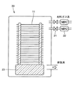
図1は本発明の洗浄処理室と成膜処理室とが一体化された装置を示す概略構成図である。本装置は、カセットローダ5、スピン式のウエット洗浄ユニット(以下、「洗浄ユニット」と記す)9が設置された洗浄ユニット室1a、UV照射ユニット室1bおよびCVD装置室2を有し、各室間の基板11の移動は、中央部のロードロック室(搬送ロボット室)3に設置された搬送ロボット4によって枚葉で行われる。ロードロック室3、UV照射ユニット室1b、洗浄ユニット室1a、CVD装置室2は、いずれも概ね密閉された緩密閉構造となっており、それぞれ配管(図示せず)によってガスを誘導できる構造を有し、ケミカルフィルタ7によって汚染物質が除去された窒素ガスまたはドライエアが導入される。各室内では、本装置外の雰囲気に対して陽圧となるように、誘導ガスの流量制御を行い、本装置外の雰囲気が混入しないようにしている。ロードロック室3に通じる各室の入口には開閉自在の扉8を設け、各室での基板処理中はロードロック室と雰囲気を分離できる構成となっている。カセットローダ5とロードロック室8との間にも開閉自在の扉8を設け、基板の受け渡し時以外は閉じておく。特に、洗浄が完了した基板のCVD装置室2への搬送時には、ロードロック室3の雰囲気を制御する必要がある。成膜処理を行うCVD装置室内においては、当然、通常の真空装置と同様に、ポンプにより真空または減圧に引けるようにされている。
【0031】
つぎに、各ユニット(装置)について説明する。図2は、UV照射ユニット室1bに設置されたUV照射ユニットの模式的断面図である。基板11のサイズに合わせたUV照射ユニット21は、150W程度の低出力型のUVランプ22が0.2本/cmの密度で備えられている。また、ステージを可動構造にして、ランプピッチの半分の振幅で、基板11を揺動しUV照射が均一に行われるようにする。このUVランプの代わりに、波長172nmのエキシマUVランプ等を用いることにより、有機物の除去効率を高めることも可能である。図3は洗浄ユニット9の模式的断面図である。ここに備えられる洗浄処理装置は、液晶表示装置の製造に一般的に用いられるインライン写真製版装置の洗浄ユニットや現像ユニットと同等の性能のものでよい。この洗浄ユニット9は、基板の回転機構、アームによるブラシ洗浄機構12、メガソニック洗浄機構などの物理洗浄と、薬液やリンス液を放出できるノズルによる化学洗浄との両方ができるアーム機構13を備える。洗浄に使用する薬液に応じて、基板支持ステージ台や薬液の飛散防止のカップの材質を耐薬液性とすることが望ましい。ここでは、薬液としてフッ酸系が使えるように、テフロンをコーティングしたステンレスを用いるのがよい。物理洗浄機構と薬液との組合せに不都合が生じる場合には、スピン式の物理洗浄ユニットを別に設けてもよい。その場合には、酸化性の薬液などを用いることも可能である。
【0032】
つぎにCVD装置の例を示す。これらのCVD装置は、どの種類のCVD装置においても、一般の液晶表示装置の製造に用いられるCVD装置と同様のものでよい。図4は、減圧CVD(LPCVD)ユニットの断面図である。このLPCVD装置30は、チャンバ内に基板を支持する石英ボート23、ポンプ(図示せず)等による減圧が可能な排気機構、および成膜ガスを導入するマスフローコントローラ(MFC)32やバルブ31を備えた配管系統を有している。また、図5に示すように、プラズマCVD(PCVD)装置では、プラズマ発生機構の付いた成膜処理室39には成膜ガスを導入するMFC32やバルブ31等を備えた配管が接続されている。また、基板11の予備加熱や冷却、さらに成膜処理室と低圧状態で基板の受け渡しが可能なように、ロードロック室36と、搬送ロボット38を設置した予備室37との二室を備えている。また、成膜処理室39はそれぞれ独立に、ポンプにより低圧に引ける排気機構を有している。このCVD装置に付け加えて、同じ雰囲気内にアモルファスシリコンから多結晶体シリコンに結晶化するレーザアニール室を配置してもよい。レーザアニール装置としては、300℃程度の低温で多結晶体シリコンを生成させる一般的な装置でよい。
【0033】
上記の装置を用いて得られる作用はつぎのとおりである。洗浄処理から成膜処理、さらにレーザアニール処理に至る工程を外気に触れることなく、自動的に連続処理することができる。この結果、基板への化学汚染やパーティクル付着を低減することができる。また、このような緩密閉構造に雰囲気を制御したガスを導入することにより、さらに汚染付着を低減することが可能である。使用するガスとしては窒素ガスまたはドライエアのような安全で比較的安価なガスでよく、ケミカルフィルタを通して汚染物質を除去したものを導入することが望ましい。各室とも緩密閉構造を採用しているので、液晶表示装置用の大型ガラス基板を処理する場合、完全密閉構造とする場合に比較して装置コストの大きな低減をはかることができる。また、本装置は、成膜処理装置にLPCVD装置を用いた場合に、とくに効果が高くなる。その理由は、LPCVD法によって成膜したアモルファスシリコンを結晶化して多結晶体シリコンを形成する場合に、LPCVDによる成膜速度がとくに遅く、下地の汚染の影響が大きく現れるからである。この汚染の影響により、多結晶体シリコンの結晶性が変動し易く、この結果、完成したTFTの特性は汚染の影響を強く受ける。本実施の形態の装置を用いれば、上記の変動を抑制して安定した特性のTFTを作り込むことが可能となる。
【0034】
さらに装置構成として、搬送ロボットを中心に各ユニットを配置したことにより、装置が非常にコンパクトになり、装置の省スペース化が可能となる。また、本実施の形態では、UV照射ユニットと他のウエット洗浄ユニットとの両方を用いたために、有機物および金属の汚染を確実に防止することができる。また、酸化性の処理液を用いると、有機物の除去効果がさらに向上する。しかし、とくに汚染を有機物に限定してよい場合には、洗浄ユニットとしてUV照射ユニットのみでよい。この場合には、装置の大きさは、従来の成膜装置の搬送ロボットと成膜室との間にUV照射ユニットを取り付けただけの非常なコンパクトな装置とすることができ、省スペースの効果を上げることができる。
【0035】
(実施の形態2)
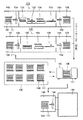
図6は、実施の形態2における製造装置の概略構成図である。洗浄装置は、液晶表示装置の製造に用いられてきた従来の洗浄装置でよく、UV照射ユニット51、ブラシ洗浄やメガソニック洗浄等の物理洗浄ユニット52、薬液による化学洗浄ユニット53、水洗ユニット54、乾燥ユニット55を備えている。成膜処理室2には、実施の形態1で説明したものと同等の性能のCVD装置が備えられる。洗浄処理室44のアンローダ43には、密閉可能なゴムパッキング付きの扉を備えたカセット18内に基板11を入れ、カセットの扉を閉じることによってカセット内に基板を密封封入する機構(図示せず)が備えられている。また、成膜処理室2のローダ46においては、密閉カセットの扉を開ける機構(図示せず)が備えられている。この密閉カセット18は洗浄処理室から成膜処理室まで、AGV等によって搬送してもよいし、洗浄処理室から成膜処理室までコンベアで自動搬送してもよい。
【0036】
さらに洗浄処理室のアンローダ45と成膜処理室のローダ46とは、入口と出口との両方に開閉自在の扉8を備え、扉を閉じた状態において概ね密閉構造となる緩密閉構造を有する。さらに、これらのアンローダ45およびローダ46には、ケミカルフィルタ7を通った窒素ガスやドライエアを誘導し、流量制御により装置外に対して陽圧を保ち、装置外の雰囲気が混入しない構造となっている。
【0037】
密閉カセット内の雰囲気としては、洗浄処理室のアンローダ45の雰囲気であるドライエアをそのまま封入してもよい。または、アンローダ45の雰囲気とは別に汚染物質を除去した窒素ガスまたはドライエアを直接カセット内に送り込んで封入してもよく、このほうがカセット内の雰囲気の管理を確実に実施できる。また、密閉後にカセット内を103Pa以下程度に真空引きしても、雰囲気の汚染物質を1/100程度に低減できるので、基板に付着する汚染物質を十分に低くすることが可能である。
【0038】
別の方法として、図7に示すように、洗浄室のアンローダ45と成膜室のローダ46との間を概ね密閉構造の通路48として、この緩密閉構造の通路48に対して雰囲気制御を行うようにしてもよい。この構成によれば、上記の密閉カセット18における密閉機構および密閉カセットに対する開閉機構を省略することができる。この場合にも、実施の形態1において説明したように、液晶表示装置用の大型ガラス基板の処理において、完全に密閉する構造に比較して装置コストを大きく低減することができる。
【0039】
なお、実施の形態1および2ともに、成膜装置としてCVD装置を用いる場合を説明したが、洗浄後のパーティクル付着が歩留り低下につながるスパッタリング装置についても、本発明が適用できることは言うまでもない。
【0040】
(実施の形態3)
つぎに実施の形態1または2に示す製造装置にレーザアニール室を付け加えた本発明に係る装置を用いて、液晶表示装置の駆動回路部の多結晶体シリコンTFTを製造する方法を説明する。まず、図8に示すように、ガラス基板11の表面に、例えば、PECVDによって下地膜としてシリコン窒化膜とシリコン酸化膜との2層膜62を連続形成する。つぎに、上記の洗浄・成膜・アニール一体型の装置を用いて、洗浄処理とLPCVD装置による成膜処理とレーザアニール処理とを連続して行う。洗浄処理としては、UV照射処理、ブラシ洗浄およびメガソニック洗浄を行い、その後、オゾン水またはHF系洗浄液を用いて薬液洗浄を行う。この後、基板を外気に触れないようにして成膜処理室に搬送して成膜処理を行う。成膜処理としては、アモルファスシリコン膜を図4に示したLPCVD装置によって60nm程度形成する。さらに、外気にさらされることなく、上記装置に付け加えて設けたレーザアニール装置によってトランジスタのチャネル部のアモルファスシリコンをアニールして多結晶体シリコンとした後、図8に示すように、ドライエッチングによりパターニングしてトランジスタ領域64を形成する。つぎに、図9に示すように、ゲート絶縁膜として、例えば、TEOS(Tetra Ethyl Ortho Silicate)PECVDによりシリコン酸化膜65を70nm程度形成する。この後、レジストを設けn型トランジスタ76のチャネル領域69の両端に燐イオンを低濃度に注入してn-型不純物領域のLDD(Lightly Doped Domain)75を形成する。次に、例えば、Cr膜を成膜し、パターニングしてゲート電極66を形成する。その後、燐イオン、ボロンイオンを順に注入してソース/ドレイン領域となるn+型不純物領域67およびp型不純物領域を形成し、それぞれn型トランジスタ76およびp型トランジスタ77を作り込む。燐イオンおよびボロンイオンの注入時には、n型トランジスタには燐イオンが、またp型トランジスタにはボロンイオンが注入されるようにする。
【0041】
つぎに、図10に示すように、保護膜としてTEOS PECVDによりシリコン酸化膜71を形成した後、400℃で活性化アニールを行う。保護膜にコンタクトホールをドライエッチングにより開口し、Cr膜を100nm、またAl系合金膜を400nm、さらにCr膜を100nm連続してスパッタにより積層し、パターニングしてソース/ドレイン電極72を形成する。この後、水素プラズマ中でチャネル部を対象に多結晶体シリコンの水素化処理を行い、特性の向上や安定化をした後に、シリコン窒化膜等により絶縁膜74を形成する。このようなプロセスで作製したn型トランジスタ76およびp型トランジスタ77を組み合わせて、駆動回路に備えられるCMOS回路を構成する。
【0042】
上記の駆動回路領域の作製中に、同じガラス基板に作製される表示画素領域についても同じ種類の層は駆動回路領域と同じタイミングで成膜処理がなされる。図11に示すように、表示画素領域に形成される素子部分は、画素用の2個のn型トランジスタからなる画素トランジスタ89、および上部電極86、下部電極85を有する容量88が形成される点を除いて、駆動回路領域の素子部分と変わるところはない。表示画素領域における成膜手順は、駆動回路領域の成膜と平行して一体的に進行する。下部ガラス基板側において、絶縁膜74が形成された後、表示画素領域では画素電極87がコンタクトホールを介して表示画像領域のn型トランジスタに接続され、さらにその上に配向膜84が形成される。表示画素領域の上部ガラス基板81には、カラーフィルタ82、対向電極83が積層され、その上に配向膜84が形成される。この後、上記の処理がなされた上部および下部のガラス基板をギャップ間隔を保って貼り合わせ、そのギャップに液晶78を注入することによって液晶表示装置を完成する(図11)。
【0043】
上記の方法で製造された液晶表示装置では、チャネル部の多結晶体シリコンの上層および下層からの有機物や金属による汚染を防止することができる。このため、レーザアニール後に多結晶体シリコン中へ金属不純物が混入することによるしきい値電圧Vthの変動や、下地の不純物の影響によって結晶化時の結晶成長が変動する等に起因するTFTの特性劣化が発生しなくなった。また、各成膜前のパーティクルの再付着も低減することができた。この結果、TFTのしきい値電圧のばらつき、容量絶縁膜の耐圧とも問題なく、製品の歩留り、耐久性、信頼性等のすべての面での向上が可能となった。本実施の形態では、とくに特性面での効果の高い、チャネル部のシリコンの成膜工程およびレーザアニール工程において、実施の形態1における装置にレーザアニール装置を付け加えた装置を導入した。しかし、洗浄後のパーティクル再付着の低減効果があるので、その他のスパッタ成膜等に応用することによってスパッタ成膜における歩留りを向上することが可能となる。
【0044】
(実施の形態4)
実施の形態3に示した液晶表示装置について、実施の形態2における装置を用いることにより、薬液槽等で基板を洗浄処理することができるので、強酸性の薬液や高温の薬液を温度制御して洗浄することができる。例えば、半導体装置の製造によく使用されるRCA洗浄液、すなわちH2SO4+H2O2+H2Oからなる洗浄液や、NH3+H2O2+H2O、HCl+H2O2+H2O、HF+H2O等の洗浄液を用いることができる。これらの洗浄液は、除去対象物やガラス基板表面へのダメージ具合等に応じて適宜組み合わせて、それぞれの処理を常温〜100℃程度までの適当な温度で行う。これらの洗浄処理によって、汚染物質を除去し、その後、汚染物質を付着させずに成膜およびアニールすることが可能となる。上記の方法によって形成された液晶表示装置では、チャネル部の上層および下層において有機物や金属による汚染がなく、レーザアニール後の多結晶体シリコン中の金属不純物によるVthの変動や結晶化における結晶性への影響がないので、TFTの特性劣化が発生しなくなる。また、各成膜前のパーティクルの再付着も低減することができる。この結果、TFTのしきい値電圧Vthのばらつき、容量絶縁膜の耐圧とも問題なくなり、製品の歩留り、耐久性、信頼性のすべての面での向上を得ることができる。
【0045】
上記において、本発明の実施の形態について説明を行ったが、上記に開示された本発明の実施の形態は、あくまで例示であって、本発明の範囲はこれら発明の実施の形態に限定されない。本発明の範囲は、特許請求の範囲の記載によって示され、さらに特許請求の範囲の記載と均等の意味および範囲内でのすべての変更を含む。
【0046】
【発明の効果】
本発明の液晶表示装置の製造装置を用いることにより、基板を洗浄後、化学的汚染やパーティクル等の再付着を受けずに液晶表示装置を製造することができる。この結果、しきい値電圧の変動等に起因する歩留り低下を生じることがなくなる。また、ロードロック室を中心に洗浄処理室および成膜処理室を配置することにより、本発明の装置は非常にコンパクトになり、液晶表示装置の製造現場の省スペースに寄与することが期待される。
【図面の簡単な説明】
【図1】 実施の形態1における洗浄・成膜処理一体型の液晶表示装置の製造装置の概略構成図である。
【図2】 図1におけるUV照射ユニットの模式的断面図である。
【図3】 図1におけるスピン式ウエット洗浄ユニットの模式的断面図である。
【図4】 実施の形態1におけるLPCVD装置の概略構成図である。
【図5】 実施の形態1におけるPCVD装置の概略構成図である。
【図6】 実施の形態2において洗浄処理室から成膜処理室に基板を搬送する機構を説明する図である。
【図7】 実施の形態2において洗浄処理室から成膜処理室に基板を搬送する、もう一つの機構を説明する図である。
【図8】 実施の形態3において、ガラス基板の上に下地膜を形成し、アモルファスシリコン膜を形成した後、アニールして結晶化し、トランジスタ部をパターニングした段階の断面図である。
【図9】 ゲート絶縁膜を成膜し、ソース/ドレイン領域に不純物イオンを注入し、ゲート配線を形成した段階の断面図である。
【図10】 層間絶縁膜、ソース/ゲート電極および保護絶縁膜を形成した段階の断面図である。
【図11】 液晶表示装置の駆動回路領域および表示画素領域の断面図である。
【図12】 洗浄処理工程から成膜処理工程に至る、従来の搬送工程の雰囲気を示す図である。
【符号の説明】
1a,1b 洗浄処理室、2 成膜処理室(CVD装置室)、3 ロードロック室、4 搬送ロボット、5 カセットロード/アンロード、6 カセット、7ケミカルフィルタ、8 扉、9 スピン式洗浄ユニット、11 基板(基板)、12 ブラシ洗浄機構、13 物理洗浄および薬液洗浄機構、18 密封カセット、21 UV照射ユニット、22 UVランプ、23 石英ボート、30 LPCVD、31 バルブ、32 MFC、35 PCVD、36 ロードロック室、37 予備室、38 搬送ロボット、39 成膜処理室、43 ローダ、44 洗浄処理室、45 アンローダ、46 ローダ/アンローダ、48 緩密閉通路、51 UV照射ユニット、52 物理洗浄ユニット(ブラシ洗浄、メガソニック洗浄)、53 薬液洗浄ユニット、54 水洗ユニット、55 乾燥ユニット、64 トランジスタ部、65 ゲート絶縁膜、66 ゲート配線、67n+型不純物領域、68 p型不純物領域、69 チャネル領域、71 層間絶縁膜、72 金属配線、74 保護膜、75 n-型不純物領域、76 n型トランジスタ、77 p型トランジスタ、78 液晶、81 上部ガラス基板、82 カラーフィルタ、83 対向電極、84 配向層、85 容量下部電極、86 容量上部電極、87 画素電極、88 容量、89 画素トランジスタ。[0001]
BACKGROUND OF THE INVENTION
The present invention relates to a liquid crystal display device manufacturing apparatus and a liquid crystal display device manufacturing method, and more particularly to a driving circuit integrated liquid crystal display device and a driving circuit integrated liquid crystal display device manufacturing method.
[0002]
[Prior art]
In a liquid crystal display device integrated with a drive circuit using a thin film transistor (TFT), the TFT in the pixel region only plays two roles of charging the pixel electrode and switching the charge. For this reason, the required performance for the TFT in the pixel region does not require fine threshold voltage control as required for a general semiconductor device. Therefore, amorphous silicon is sufficient for the thin film semiconductor used for the TFT in the pixel region.
[0003]
In recent years, technological development using a polycrystalline silicon TFT formed by laser annealing amorphous silicon has been performed, and liquid crystal display devices using this polycrystalline silicon TFT have been actively manufactured. This type of liquid crystal display device has an advantage that the drive circuit region and the pixel region are integrally formed, thereby reducing the cost and increasing the definition of the display pixel. Since this polycrystalline silicon TFT needs to have the characteristics required for the elements of the drive circuit, it is necessary to maintain a highly accurate threshold voltage. For this reason, new issues have arisen.
[0004]
In the manufacturing process of a conventional liquid crystal display device using amorphous silicon, a cleaning process is usually performed in order to remove foreign substances and improve the adhesion of the amorphous silicon film in the pre-process of the amorphous silicon film forming process. FIG. 12 is a diagram showing an atmospheric environment of a path from a conventional cleaning process to a film forming process. The cleaning process includes a
[0005]
[Problems to be solved by the invention]
However, as can be seen from the fact that the substrate is open to the clean room atmosphere, the chemical contamination of the substrate surface has not been adequately controlled. The influence of such chemical contamination is at a level that does not cause any problem in the amorphous silicon TFT used only in the pixel region. However, in the polycrystalline silicon TFT constituting the drive circuit, the doping effect due to contamination of metals or the like, and the influence on the crystal grain growth of polycrystalline silicon due to organic contamination, etc. occur. As a result, the threshold voltage fluctuates, causing variations in the substrate, causing a malfunction in the drive circuit, resulting in a decrease in yield.
[0006]
SUMMARY OF THE INVENTION Accordingly, an object of the present invention is to provide a liquid crystal display device manufacturing apparatus and a liquid crystal display device capable of preventing chemical contamination resulting from contact with a clean room atmosphere and preventing threshold voltage fluctuations and the like from occurring. It is in providing the manufacturing method of.
[0007]
[Means for Solving the Problems]
The apparatus for manufacturing a liquid crystal display device according to claim 1 of the present invention comprises:Cleaning process chamber for cleaning substrates of liquid crystal display devicesWhen,Cleaning treatment roomA film forming chamber for performing a film forming process on the substrate cleaned inCleaning treatment roomAnd an outside air blocking transfer means for transferring the substrate to the film forming chamber without being exposed to the outside air.The outside air blocking transfer means includes a substrate carry-in means for carrying a substrate cleaned in the cleaning processing chamber into a cassette capable of accommodating a plurality of substrates without exposing the substrate to the outside air, and a substrate for taking out the substrate from the cassette in the film forming processing chamber. Taking-out means. The outside air blocking transfer unit includes an outside air blocking path that is a path through which the substrate is transferred from the cleaning processing chamber to the film forming chamber and is blocked from outside air. The outside air blocking transfer means is formed so as to be able to transport the cassette. The outside air blocking passage has a loosely sealed structure that is generally shielded from outside air. Inside the outside air blocking passage, an inert gas inert to the substrate is maintained at a positive pressure with respect to the outside air. Yes.
[0008]
This configuration prevents chemical contamination since it is not exposed to a clean room atmosphere after cleaning. For this reason, the threshold voltage does not fluctuate due to a doping effect due to metal contamination or a variation in crystal grain size due to organic contamination. Further, it is possible to prevent adhesion of particles after cleaning. As a result, it is possible to avoid a situation in which the product yield decreases due to malfunction of the drive circuit. In addition, said board | substrate refers to the board | substrate defined previously.
[0009]
In the manufacturing apparatus of the liquid crystal display device of
[0010]
Moreover, it is preferable to provide a transporter for transporting the substrate in the outside air blocking passage.With this configuration, it becomes easy to automatically transport the substrate without exposing it to the outside air. Further, by automating, it becomes easy to shorten the waiting time and the conveyance time, and it becomes possible to increase the production efficiency.
[0011]
In the apparatus for manufacturing a liquid crystal display device according to
[0012]
With this configuration, the substrate is transferred from the cleaning processing chamber to the film forming processing chamber while being stored in the sealed cassette without being exposed to the outside air, so that chemical contamination and particle adhesion after cleaning can be avoided. Note that the conveyance of the sealed cassette from the unloading section of the cleaning processing chamber to the loading section of the film forming processing chamber may be performed by a transport machine such as AGV, or may be performed manually.
[0013]
In the apparatus for manufacturing a liquid crystal display device according to
[0014]
With this configuration, the substrate can be continuously transferred from the cassette load chamber to the film forming chamber through the cleaning chamber without being exposed to the outside air. As a result, it is possible to shorten the film forming process and increase the efficiency while preventing chemical contamination and particle adhesion after cleaning. Further, it is possible to realize a space saving in a clean room by downsizing an apparatus incorporating the above-described chambers. In the apparatus according to claims 1 to 4, the outside air blocking passage or the inside of the sealed cassette has 10 outside air.ThreeDesirably, the atmosphere is reduced to Pa or lower, a nitrogen gas atmosphere, or a dry air atmosphere. The substrate is not subjected to chemical contamination or particle adhesion after cleaning in the above atmosphere, and since these atmospheres can be realized at low cost, the manufacturing cost is not increased. Nitrogen gas, dry air, etc. are referred to as inert gas.
[0015]
According to a fifth aspect of the present invention, there is provided a manufacturing apparatus for a liquid crystal display device according to any one of the first to fourth aspects, wherein the processing chamber communicates with the outside air blocking passage and is blocked from outside air, and the substrate is annealed. An annealing chamber is further provided.
[0016]
With this configuration, the formed film can be annealed without being exposed to the outside air. For this reason, it is possible to obtain a polycrystalline silicon film by annealing treatment in a state where chemical contamination of the formed amorphous silicon film is prevented.
[0017]
According to a sixth aspect of the present invention, there is provided an apparatus for manufacturing a liquid crystal display device according to the fifth aspect, further comprising an optical alignment unit capable of performing laser annealing on the substrate in the annealing chamber.
[0018]
With this configuration, the amorphous silicon film can be a polycrystalline silicon film having a large crystal grain size at a low temperature. Therefore, it is possible to manufacture a TFT having performance that can be used for a drive circuit while preventing chemical contamination.
[0019]
According to a seventh aspect of the present invention, there is provided the apparatus for manufacturing a liquid crystal display device according to any one of the first to sixth aspects, wherein the film forming chamber is in communication with the first film forming chamber communicating with the outside air blocking passage. And a second film forming treatment chamber.
[0020]
With this configuration, the chemical contamination-agnostic film formed in the first film formation chamber, such as polycrystalline silicon, is chemically contaminated both from the base film side and from the upper side, that is, the gate insulating film side. Can be prevented. As a result, a stable threshold voltage can be obtained, and the yield can be improved.
[0021]
In the manufacturing apparatus of the liquid crystal display device of
[0022]
This configuration can be realized at a lower cost than a strict sealing structure. For this reason, chemical contamination and particle adhesion can be prevented at a low cost, and the effect of yield improvement can be further enjoyed.
[0023]
The method of manufacturing a liquid crystal display device according to claim 10 of the present invention is as follows.,A substrate having a base film on a glass substrateCleaning treatment roomChargedWashThe cleaning process and the cleaned substrate,Cleaning treatment roomTaken out from the chamber and placed in the film formation chamber without exposure to the outside airTransfer processAnd the substrate in the film formation chamberOn top of theForming an amorphous silicon film.The transfer step includes a step of inserting and transporting the substrate into a cassette that can accommodate a plurality of substrates. The transfer step includes a step of carrying the substrate cleaned in the cleaning processing chamber into the cassette without exposing it to the outside air, and a step of taking the substrate out of the cassette in the film forming processing chamber. The transfer process has a loosely sealed structure that is generally shielded from the outside air, and is performed through an outside air blocking passage in which an inert gas inert to the substrate is maintained at a positive pressure with respect to the outside air. .
[0024]
With this configuration, since the amorphous silicon film that dislikes chemical contamination is not subjected to chemical contamination or particle adhesion from the lower side, it is possible to maintain high yield without causing malfunction.
[0025]
In the method of manufacturing a liquid crystal display device according to
[0026]
With this configuration, high definition can be achieved in the pixel region, and a low-cost and stable high-accuracy threshold voltage can be secured in the drive transistor in the drive circuit region. In addition, the pixel region and the drive circuit region can be formed integrally, and downsizing which is important in the liquid crystal display device can be realized.
[0027]
In the manufacturing method of the liquid crystal display device of
[0028]
With this configuration, the polycrystalline silicon is not subjected to chemical contamination or particle adhesion after cleaning from both the base film side and the gate insulating film side. As a result, fluctuations in the threshold voltage can be further suppressed, and it is possible to more reliably avoid a decrease in yield.
[0029]
DETAILED DESCRIPTION OF THE INVENTION
Next, embodiments of the present invention will be described with reference to the drawings.
[0030]
(Embodiment 1)
FIG. 1 is a schematic configuration diagram showing an apparatus in which a cleaning processing chamber and a film forming processing chamber of the present invention are integrated. This apparatus has a cassette loader 5, a
[0031]
Next, each unit (device) will be described. FIG. 2 is a schematic cross-sectional view of the UV irradiation unit installed in the UV
[0032]
Next, an example of a CVD apparatus is shown. These CVD apparatuses may be similar to the CVD apparatus used for manufacturing a general liquid crystal display device in any type of CVD apparatus. FIG. 4 is a cross-sectional view of a low pressure CVD (LPCVD) unit. The
[0033]
The effects obtained using the above-described apparatus are as follows. The processes from the cleaning process to the film forming process and further to the laser annealing process can be automatically and continuously performed without touching the outside air. As a result, chemical contamination and particle adhesion to the substrate can be reduced. Moreover, it is possible to further reduce the adhesion of contamination by introducing a gas whose atmosphere is controlled into such a loosely sealed structure. The gas used may be a safe and relatively inexpensive gas such as nitrogen gas or dry air, and it is desirable to introduce a gas from which contaminants have been removed through a chemical filter. Since each chamber employs a loosely sealed structure, when processing a large glass substrate for a liquid crystal display device, the apparatus cost can be greatly reduced as compared with a completely sealed structure. In addition, this apparatus is particularly effective when an LPCVD apparatus is used as the film forming apparatus. The reason is that when amorphous silicon deposited by the LPCVD method is crystallized to form polycrystalline silicon, the deposition rate by LPCVD is particularly slow, and the influence of contamination of the substrate appears greatly. Due to the influence of this contamination, the crystallinity of the polycrystalline silicon is likely to fluctuate, and as a result, the characteristics of the completed TFT are strongly affected by the contamination. By using the device of this embodiment mode, it is possible to suppress the above-described fluctuations and make a TFT having stable characteristics.
[0034]
Furthermore, since the units are arranged around the transfer robot as the device configuration, the device becomes very compact, and the space of the device can be saved. Further, in the present embodiment, since both the UV irradiation unit and the other wet cleaning unit are used, it is possible to reliably prevent contamination of organic matter and metal. Further, when an oxidizing treatment liquid is used, the organic substance removal effect is further improved. However, particularly when the contamination may be limited to organic matter, only the UV irradiation unit is required as the cleaning unit. In this case, the size of the apparatus can be a very compact apparatus in which a UV irradiation unit is simply installed between the transfer robot of the conventional film forming apparatus and the film forming chamber. Can be raised.
[0035]
(Embodiment 2)
FIG. 6 is a schematic configuration diagram of a manufacturing apparatus according to the second embodiment. The cleaning device may be a conventional cleaning device that has been used in the manufacture of liquid crystal display devices, such as a
[0036]
Further, the
[0037]
As the atmosphere in the sealed cassette, dry air that is the atmosphere of the
[0038]
As another method, as shown in FIG. 7, an atmosphere control is performed for the loosely-sealed
[0039]
Although the case where a CVD apparatus is used as the film forming apparatus has been described in both
[0040]
(Embodiment 3)
Next, a method for manufacturing a polycrystalline silicon TFT in a drive circuit portion of a liquid crystal display device using the apparatus according to the present invention in which a laser annealing chamber is added to the manufacturing apparatus shown in
[0041]
Next, as shown in FIG. 10, after forming a
[0042]
During the production of the drive circuit region, the same kind of layer is formed at the same timing as the drive circuit region in the display pixel region produced on the same glass substrate. As shown in FIG. 11, the element portion formed in the display pixel region is formed with a
[0043]
In the liquid crystal display device manufactured by the above method, contamination by organic substances or metals from the upper and lower layers of polycrystalline silicon in the channel portion can be prevented. For this reason, TFT characteristics caused by fluctuations in threshold voltage Vth due to metal impurities mixed into polycrystalline silicon after laser annealing, and crystal growth during crystallization due to the influence of underlying impurities, etc. Deterioration no longer occurs. Moreover, the reattachment of particles before each film formation could be reduced. As a result, it is possible to improve all aspects of product yield, durability, reliability, etc. without any problem in variations in the threshold voltage of the TFT and withstand voltage of the capacitor insulating film. In the present embodiment, an apparatus in which a laser annealing apparatus is added to the apparatus in the first embodiment is introduced in the silicon film forming process and the laser annealing process in the channel portion, which are particularly effective in terms of characteristics. However, since there is an effect of reducing the reattachment of particles after cleaning, it is possible to improve the yield in sputtering film formation by applying to other sputtering film formation.
[0044]
(Embodiment 4)
As for the liquid crystal display device shown in
[0045]
Although the embodiments of the present invention have been described above, the embodiments of the present invention disclosed above are merely examples, and the scope of the present invention is not limited to these embodiments. The scope of the present invention is indicated by the description of the scope of claims, and further includes meanings equivalent to the description of the scope of claims and all modifications within the scope.
[0046]
【The invention's effect】
By using the apparatus for manufacturing a liquid crystal display device of the present invention, a liquid crystal display device can be manufactured without being subjected to chemical contamination or redeposition of particles after cleaning the substrate. As a result, the yield does not decrease due to threshold voltage fluctuations or the like. In addition, by disposing the cleaning processing chamber and the film forming processing chamber around the load lock chamber, the apparatus of the present invention becomes very compact and is expected to contribute to space saving at the manufacturing site of the liquid crystal display device. .
[Brief description of the drawings]
1 is a schematic configuration diagram of an apparatus for manufacturing a liquid crystal display device integrated with a cleaning and film formation process in Embodiment 1. FIG.
FIG. 2 is a schematic cross-sectional view of the UV irradiation unit in FIG.
FIG. 3 is a schematic cross-sectional view of the spin-type wet cleaning unit in FIG.
4 is a schematic configuration diagram of an LPCVD apparatus according to Embodiment 1. FIG.
FIG. 5 is a schematic configuration diagram of a PCVD apparatus in the first embodiment.
6 is a diagram illustrating a mechanism for transporting a substrate from a cleaning processing chamber to a deposition processing chamber in
7 is a diagram illustrating another mechanism for transporting a substrate from a cleaning chamber to a film formation chamber in
8 is a cross-sectional view of a stage where a base film is formed on a glass substrate, an amorphous silicon film is formed, crystallized by annealing, and a transistor portion is patterned in
FIG. 9 is a cross-sectional view of a stage where a gate insulating film is formed, impurity ions are implanted into source / drain regions, and a gate wiring is formed.
FIG. 10 is a cross-sectional view at a stage where an interlayer insulating film, a source / gate electrode, and a protective insulating film are formed.
FIG. 11 is a cross-sectional view of a driving circuit region and a display pixel region of a liquid crystal display device.
FIG. 12 is a diagram showing an atmosphere of a conventional transfer process from a cleaning process to a film forming process.
[Explanation of symbols]
1a, 1b Cleaning processing chamber, 2 Film formation processing chamber (CVD chamber), 3 Load lock chamber, 4 Transfer robot, 5 Cassette loading / unloading, 6 Cassette, 7 Chemical filter, 8 Door, 9 Spin cleaning unit, 11 substrate (substrate), 12 brush cleaning mechanism, 13 physical cleaning and chemical cleaning mechanism, 18 sealed cassette, 21 UV irradiation unit, 22 UV lamp, 23 quartz boat, 30 LPCVD, 31 bulb, 32 MFC, 35 PCVD, 36 load Lock chamber, 37 Preparatory chamber, 38 Transfer robot, 39 Deposition processing chamber, 43 Loader, 44 Cleaning processing chamber, 45 Unloader, 46 Loader / unloader, 48 Loosely sealed passage, 51 UV irradiation unit, 52 Physical cleaning unit (Brush cleaning) , Megasonic cleaning), 53 Chemical cleaning unit, 54 Cleaning unit, 55 Drying unit, 64 Transistor part, 65 Gate insulating film, 66 Gate wiring, 67n + type impurity region, 68 p-type impurity region, 69 channel region, 71 Interlayer insulating film, 72 Metal wiring, 74 Protective film, 75 n-type impurity region, 76 n-type transistor, 77 p-type transistor, 78 liquid crystal, 81 upper glass substrate, 82 color filter, 83 counter electrode, 84 orientation layer, 85 capacitive lower electrode, 86 capacitive upper electrode, 87 pixel electrode, 88 capacitors, 89 pixel transistors.
Claims (12)
前記洗浄処理室で洗浄された前記基板に対して成膜処理を行う成膜処理室と、
前記洗浄処理室から前記成膜処理室へ前記基板を外気にさらすことなく移送する外気遮断移送手段とを備え、
前記外気遮断移送手段は、前記洗浄処理室で洗浄された前記基板を外気にさらすことなく、複数の前記基板が収容可能なカセット内に搬入する基板搬入手段と、前記成膜処理室において前記基板を前記カセット内から取り出す基板取出し手段とを含み、
前記外気遮断移送手段は、前記洗浄処理室から前記成膜処理室まで前記基板が移送される通路であって外気が遮断された外気遮断通路を含み、
前記外気遮断移送手段は、前記カセットを搬送可能に形成され、
前記外気遮断通路は、外気から概ね遮断される程度の緩密閉構造を有しており、前記外気遮断通路の内部では、前記基板に対して不活性の不活性ガスが外気に対して陽圧に保たれている、液晶表示装置の製造装置。 A cleaning treatment chamber for cleaning the substrate of the liquid crystal display device;
A deposition treatment chamber for performing a film forming process with respect to the substrate that has been cleaned with the cleaning chamber,
An outside air blocking transfer means for transferring the substrate from the cleaning chamber to the film forming chamber without being exposed to the outside air ,
The outside air blocking transfer means includes a substrate carry-in means for carrying the substrate cleaned in the cleaning processing chamber into a cassette that can accommodate a plurality of substrates without exposing the substrate to the outside air, and the substrate in the film forming processing chamber. A substrate take-out means for taking out from the cassette,
The outside air blocking transfer means includes a outside air blocking passage that is a passage through which the substrate is transferred from the cleaning processing chamber to the film forming processing chamber and is blocked from outside air,
The outside air blocking transfer means is formed to be able to transport the cassette,
The outside air blocking passage has a loosely sealed structure that is generally shielded from outside air. Inside the outside air blocking passage, an inert gas that is inert to the substrate has a positive pressure with respect to the outside air. A liquid crystal display manufacturing apparatus that is maintained .
前記洗浄が行われた前記基板を、前記洗浄処理室から取り出し、外気にさらすことなく成膜処理室に装入する移送工程と、
前記成膜処理室において前記基板の上にアモルファスシリコン膜を成膜する工程とを備え、
前記移送工程は、複数の前記基板が収容可能なカセットに前記基板を挿入して搬送する工程を含み、
前記移送工程は、前記洗浄処理室で洗浄された前記基板を外気にさらすことなく、カセット内に搬入する工程と、前記成膜処理室において前記基板を前記カセット内から取り出す工程とを含み、
前記移送工程は、外気から概ね遮断される程度の緩密閉構造を有しており、内部では前 記基板に対して不活性の不活性ガスが外気に対して陽圧に保たれている外気遮断通路を通して行なう、液晶表示装置の製造方法。Was charged a substrate having a base film on a glass substrate to the cleaning processing chamber, and performing a cleaning process,
The transfer step of taking out the cleaned substrate from the cleaning processing chamber and charging it into the film forming processing chamber without exposing to the outside air;
Forming an amorphous silicon film on the substrate in the film formation chamber ,
The transfer step includes a step of inserting and transporting the substrate into a cassette that can accommodate a plurality of the substrates,
The transfer step includes a step of carrying the substrate cleaned in the cleaning processing chamber into a cassette without exposing the substrate to outside air, and a step of taking the substrate out of the cassette in the film forming processing chamber,
It said transfer step has a loose sealed structure to the extent that is substantially isolated from the atmosphere, the outside air blocking the inert gas inert to the previous SL substrate Inside is kept positive pressure relative to the outside air A method for manufacturing a liquid crystal display device , which is performed through a passage .
Priority Applications (4)
| Application Number | Priority Date | Filing Date | Title |
|---|---|---|---|
| JP2000017223A JP3998386B2 (en) | 2000-01-26 | 2000-01-26 | Liquid crystal display device manufacturing apparatus and liquid crystal display device manufacturing method |
| US09/715,022 US6461437B1 (en) | 2000-01-26 | 2000-11-20 | Apparatus used for fabricating liquid crystal device and method of fabricating the same |
| CNB001364952A CN1196173C (en) | 2000-01-26 | 2000-12-27 | Device and method for manufacture of liquid crystal display |
| KR10-2001-0003540A KR100381807B1 (en) | 2000-01-26 | 2001-01-22 | Apparatus used for fabricating liquid crystal device and method of fabricating the same |
Applications Claiming Priority (1)
| Application Number | Priority Date | Filing Date | Title |
|---|---|---|---|
| JP2000017223A JP3998386B2 (en) | 2000-01-26 | 2000-01-26 | Liquid crystal display device manufacturing apparatus and liquid crystal display device manufacturing method |
Publications (3)
| Publication Number | Publication Date |
|---|---|
| JP2001210693A JP2001210693A (en) | 2001-08-03 |
| JP2001210693A5 JP2001210693A5 (en) | 2005-04-07 |
| JP3998386B2 true JP3998386B2 (en) | 2007-10-24 |
Family
ID=18544249
Family Applications (1)
| Application Number | Title | Priority Date | Filing Date |
|---|---|---|---|
| JP2000017223A Expired - Fee Related JP3998386B2 (en) | 2000-01-26 | 2000-01-26 | Liquid crystal display device manufacturing apparatus and liquid crystal display device manufacturing method |
Country Status (4)
| Country | Link |
|---|---|
| US (1) | US6461437B1 (en) |
| JP (1) | JP3998386B2 (en) |
| KR (1) | KR100381807B1 (en) |
| CN (1) | CN1196173C (en) |
Families Citing this family (15)
| Publication number | Priority date | Publication date | Assignee | Title |
|---|---|---|---|---|
| TWI270626B (en) * | 2002-04-23 | 2007-01-11 | Display Mfg Service Co Ltd | Wet processing bath and fluid supplying system for liquid crystal display manufacturing equipment |
| JP4219799B2 (en) * | 2003-02-26 | 2009-02-04 | 大日本スクリーン製造株式会社 | Substrate processing equipment |
| JP4833512B2 (en) * | 2003-06-24 | 2011-12-07 | 東京エレクトロン株式会社 | To-be-processed object processing apparatus, to-be-processed object processing method, and to-be-processed object conveyance method |
| DE10358275A1 (en) * | 2003-12-11 | 2005-07-21 | Wiessner Gmbh | Apparatus and method for cleaning at least one process chamber for coating at least one substrate |
| US7422653B2 (en) * | 2004-07-13 | 2008-09-09 | Applied Materials, Inc. | Single-sided inflatable vertical slit valve |
| US8075953B2 (en) * | 2005-09-15 | 2011-12-13 | Hiap L. Ong and Kyoritsu Optronics Co., Ltd | Thin organic alignment layers with a batch process for liquid crystal displays |
| JP4765986B2 (en) * | 2007-03-23 | 2011-09-07 | 村田機械株式会社 | Transport system |
| JP5190215B2 (en) * | 2007-03-30 | 2013-04-24 | 東京エレクトロン株式会社 | Cleaning method of turbo molecular pump |
| CN102947481A (en) * | 2010-06-21 | 2013-02-27 | 株式会社爱发科 | Substrate inverting apparatus, vacuum film-forming apparatus, and substrate inverting method |
| WO2012082198A1 (en) * | 2010-12-13 | 2012-06-21 | Tp Solar, Inc. | Dopant applicator system and method of applying vaporized doping compositions to pv solar wafers |
| JP5472283B2 (en) * | 2011-12-21 | 2014-04-16 | 株式会社安川電機 | Robot arm structure and robot |
| US9443730B2 (en) * | 2014-07-18 | 2016-09-13 | Asm Ip Holding B.V. | Process for forming silicon-filled openings with a reduced occurrence of voids |
| US9837271B2 (en) | 2014-07-18 | 2017-12-05 | Asm Ip Holding B.V. | Process for forming silicon-filled openings with a reduced occurrence of voids |
| US10460932B2 (en) | 2017-03-31 | 2019-10-29 | Asm Ip Holding B.V. | Semiconductor device with amorphous silicon filled gaps and methods for forming |
| CN109712906B (en) * | 2017-10-25 | 2021-05-11 | 长鑫存储技术有限公司 | Wafer storage device with cleaning function and semiconductor production equipment |
Family Cites Families (32)
| Publication number | Priority date | Publication date | Assignee | Title |
|---|---|---|---|---|
| US4406709A (en) * | 1981-06-24 | 1983-09-27 | Bell Telephone Laboratories, Incorporated | Method of increasing the grain size of polycrystalline materials by directed energy-beams |
| NL8103979A (en) * | 1981-08-26 | 1983-03-16 | Bok Edward | METHOD AND APPARATUS FOR APPLYING A FILM LIQUID MEDIUM TO A SUBSTRATE |
| US4827954A (en) * | 1982-11-23 | 1989-05-09 | Interlab, Inc. | Automated work transfer system having an articulated arm |
| JPS6162739A (en) * | 1984-09-03 | 1986-03-31 | Sanki Eng Co Ltd | Clean tunnel |
| JPH0736418B2 (en) * | 1986-05-19 | 1995-04-19 | 富士通株式会社 | Wafer carrier |
| US4951601A (en) * | 1986-12-19 | 1990-08-28 | Applied Materials, Inc. | Multi-chamber integrated process system |
| US5024570A (en) * | 1988-09-14 | 1991-06-18 | Fujitsu Limited | Continuous semiconductor substrate processing system |
| JPH05218176A (en) * | 1992-02-07 | 1993-08-27 | Tokyo Electron Tohoku Kk | Heat treatment and transfer of article to be treated |
| US6391117B2 (en) * | 1992-02-07 | 2002-05-21 | Canon Kabushiki Kaisha | Method of washing substrate with UV radiation and ultrasonic cleaning |
| JPH05271973A (en) * | 1992-03-25 | 1993-10-19 | Orc Mfg Co Ltd | Ultraviolet cleaning method |
| JPH05315310A (en) * | 1992-05-01 | 1993-11-26 | Kawasaki Steel Corp | Method for wet cleaning of semiconductor substrate and wet cleaning equipment |
| MY109592A (en) * | 1992-11-16 | 1997-03-31 | Tokyo Electron Ltd | Method and apparatus for manufacturing a liquid crystal display substrate, and apparatus and method for evaluating semiconductor crystals. |
| DE69304038T2 (en) * | 1993-01-28 | 1996-12-19 | Applied Materials Inc | Device for a vacuum process with improved throughput |
| JP3120395B2 (en) * | 1993-03-10 | 2000-12-25 | 東京エレクトロン株式会社 | Processing equipment |
| KR100261532B1 (en) * | 1993-03-14 | 2000-07-15 | 야마시타 히데나리 | Multi-chamber system provided with carrier units |
| US5527390A (en) * | 1993-03-19 | 1996-06-18 | Tokyo Electron Kabushiki | Treatment system including a plurality of treatment apparatus |
| JP3654597B2 (en) * | 1993-07-15 | 2005-06-02 | 株式会社ルネサステクノロジ | Manufacturing system and manufacturing method |
| TW273574B (en) * | 1993-12-10 | 1996-04-01 | Tokyo Electron Co Ltd | |
| US5472086A (en) * | 1994-03-11 | 1995-12-05 | Holliday; James E. | Enclosed sealable purgible semiconductor wafer holder |
| TW294821B (en) * | 1994-09-09 | 1997-01-01 | Tokyo Electron Co Ltd | |
| JP3288200B2 (en) * | 1995-06-09 | 2002-06-04 | 東京エレクトロン株式会社 | Vacuum processing equipment |
| US5667592A (en) * | 1996-04-16 | 1997-09-16 | Gasonics International | Process chamber sleeve with ring seals for isolating individual process modules in a common cluster |
| US6039059A (en) * | 1996-09-30 | 2000-03-21 | Verteq, Inc. | Wafer cleaning system |
| JP3330300B2 (en) * | 1997-02-28 | 2002-09-30 | 東京エレクトロン株式会社 | Substrate cleaning device |
| US6045620A (en) * | 1997-07-11 | 2000-04-04 | Applied Materials, Inc. | Two-piece slit valve insert for vacuum processing system |
| JP3425592B2 (en) * | 1997-08-12 | 2003-07-14 | 東京エレクトロン株式会社 | Processing equipment |
| JPH11102849A (en) * | 1997-09-17 | 1999-04-13 | Lsi Logic Corp | Method and device for removing particles on semiconductor wafer |
| US6270582B1 (en) * | 1997-12-15 | 2001-08-07 | Applied Materials, Inc | Single wafer load lock chamber for pre-processing and post-processing wafers in a vacuum processing system |
| TW444275B (en) * | 1998-01-13 | 2001-07-01 | Toshiba Corp | Processing device, laser annealing device, laser annealing method, manufacturing device and substrate manufacturing device for panel display |
| US6270306B1 (en) * | 1998-01-14 | 2001-08-07 | Applied Materials, Inc. | Wafer aligner in center of front end frame of vacuum system |
| US6343609B1 (en) * | 1998-08-13 | 2002-02-05 | International Business Machines Corporation | Cleaning with liquified gas and megasonics |
| US6337174B1 (en) * | 1998-09-17 | 2002-01-08 | Samsung Electronics Co., Ltd. | Method of stripping a photoresist from a semiconductor substrate dimethylacetamide or a combination of monoethanolamine and dimethylsulfoxide |
-
2000
- 2000-01-26 JP JP2000017223A patent/JP3998386B2/en not_active Expired - Fee Related
- 2000-11-20 US US09/715,022 patent/US6461437B1/en not_active Expired - Lifetime
- 2000-12-27 CN CNB001364952A patent/CN1196173C/en not_active Expired - Fee Related
-
2001
- 2001-01-22 KR KR10-2001-0003540A patent/KR100381807B1/en not_active IP Right Cessation
Also Published As
| Publication number | Publication date |
|---|---|
| KR20010078048A (en) | 2001-08-20 |
| US6461437B1 (en) | 2002-10-08 |
| JP2001210693A (en) | 2001-08-03 |
| KR100381807B1 (en) | 2003-04-26 |
| CN1196173C (en) | 2005-04-06 |
| CN1307326A (en) | 2001-08-08 |
Similar Documents
| Publication | Publication Date | Title |
|---|---|---|
| JP3998386B2 (en) | Liquid crystal display device manufacturing apparatus and liquid crystal display device manufacturing method | |
| JP3880343B2 (en) | Load port, substrate processing apparatus, and atmosphere replacement method | |
| TWI514478B (en) | Method and apparatus for making a field effect type transistor | |
| KR100932815B1 (en) | Multilayer High Quality Gate Dielectric for Low Temperature Poly-Si Thin Film Transistor | |
| KR100486690B1 (en) | Substrate processing apparatus and method for controlling contamination in substrate transfer module | |
| KR101238152B1 (en) | Method for processing a substrate and method for forming a silicon-containing film | |
| US6467976B2 (en) | Coating and developing system | |
| JP6760439B2 (en) | Manufacturing method of thin film and storage medium | |
| JP5142414B2 (en) | Vacuum processing equipment | |
| JP2004119635A (en) | Method of transferring processing object | |
| TWI342071B (en) | ||
| JPH11354514A (en) | Cluster tool device and film formation method | |
| JP2001044429A (en) | Method and device for pre-process for forming gate insulating film | |
| JP2010056261A (en) | Method of manufacturing semiconductor device | |
| JP2000243802A (en) | Manufacture and equipment of semiconductor device | |
| JP4869495B2 (en) | Manufacturing method of semiconductor device | |
| JP2000021891A (en) | Substrate processor and substrate processing method | |
| TWI661472B (en) | Method for forming epitaxial layer at low temperature | |
| JP2004247573A (en) | Substrate processing method | |
| KR100293524B1 (en) | Crystallization Apparatus using Non-vacuum Process and Method thereof | |
| JPH10289910A (en) | Manufacture of semiconductor device | |
| JPH0888367A (en) | Manufacture of thin film device | |
| JP2002299427A (en) | Substrate cassette, substrate contamination prevention apparatus, manufacturing method of semiconductor device | |
| JP2006049683A (en) | Method for manufacturing semiconductor integrated circuit device | |
| JP2004125882A (en) | Method for washing substrate |
Legal Events
| Date | Code | Title | Description |
|---|---|---|---|
| A521 | Request for written amendment filed |
Free format text: JAPANESE INTERMEDIATE CODE: A523 Effective date: 20040507 |
|
| A621 | Written request for application examination |
Free format text: JAPANESE INTERMEDIATE CODE: A621 Effective date: 20040507 |
|
| A977 | Report on retrieval |
Free format text: JAPANESE INTERMEDIATE CODE: A971007 Effective date: 20060413 |
|
| A131 | Notification of reasons for refusal |
Free format text: JAPANESE INTERMEDIATE CODE: A131 Effective date: 20060912 |
|
| A521 | Request for written amendment filed |
Free format text: JAPANESE INTERMEDIATE CODE: A523 Effective date: 20061106 |
|
| A131 | Notification of reasons for refusal |
Free format text: JAPANESE INTERMEDIATE CODE: A131 Effective date: 20061205 |
|
| A521 | Request for written amendment filed |
Free format text: JAPANESE INTERMEDIATE CODE: A523 Effective date: 20070126 |
|
| TRDD | Decision of grant or rejection written | ||
| A01 | Written decision to grant a patent or to grant a registration (utility model) |
Free format text: JAPANESE INTERMEDIATE CODE: A01 Effective date: 20070731 |
|
| A61 | First payment of annual fees (during grant procedure) |
Free format text: JAPANESE INTERMEDIATE CODE: A61 Effective date: 20070807 |
|
| R150 | Certificate of patent or registration of utility model |
Free format text: JAPANESE INTERMEDIATE CODE: R150 |
|
| FPAY | Renewal fee payment (event date is renewal date of database) |
Free format text: PAYMENT UNTIL: 20100817 Year of fee payment: 3 |
|
| FPAY | Renewal fee payment (event date is renewal date of database) |
Free format text: PAYMENT UNTIL: 20110817 Year of fee payment: 4 |
|
| FPAY | Renewal fee payment (event date is renewal date of database) |
Free format text: PAYMENT UNTIL: 20110817 Year of fee payment: 4 |
|
| FPAY | Renewal fee payment (event date is renewal date of database) |
Free format text: PAYMENT UNTIL: 20120817 Year of fee payment: 5 |
|
| FPAY | Renewal fee payment (event date is renewal date of database) |
Free format text: PAYMENT UNTIL: 20120817 Year of fee payment: 5 |
|
| FPAY | Renewal fee payment (event date is renewal date of database) |
Free format text: PAYMENT UNTIL: 20130817 Year of fee payment: 6 |
|
| R250 | Receipt of annual fees |
Free format text: JAPANESE INTERMEDIATE CODE: R250 |
|
| S531 | Written request for registration of change of domicile |
Free format text: JAPANESE INTERMEDIATE CODE: R313531 |
|
| R350 | Written notification of registration of transfer |
Free format text: JAPANESE INTERMEDIATE CODE: R350 |
|
| R250 | Receipt of annual fees |
Free format text: JAPANESE INTERMEDIATE CODE: R250 |
|
| R250 | Receipt of annual fees |
Free format text: JAPANESE INTERMEDIATE CODE: R250 |
|
| LAPS | Cancellation because of no payment of annual fees |