JP3987163B2 - Data communication system - Google Patents
Data communication system Download PDFInfo
- Publication number
- JP3987163B2 JP3987163B2 JP21580697A JP21580697A JP3987163B2 JP 3987163 B2 JP3987163 B2 JP 3987163B2 JP 21580697 A JP21580697 A JP 21580697A JP 21580697 A JP21580697 A JP 21580697A JP 3987163 B2 JP3987163 B2 JP 3987163B2
- Authority
- JP
- Japan
- Prior art keywords
- bias
- signal line
- bias voltage
- devices
- data communication
- Prior art date
- Legal status (The legal status is an assumption and is not a legal conclusion. Google has not performed a legal analysis and makes no representation as to the accuracy of the status listed.)
- Expired - Lifetime
Links
Images


Landscapes
- Dc Digital Transmission (AREA)
Description
【0010】
【発明の属する技術分野】
本発明は、2つの装置間で一対の信号線に所定の共通バイアス電圧を印加しながら差動方式で両信号線を駆動することによって信号を伝送するデータ通信システムに関する。
【0020】
【従来の技術】
この種のデータ通信システムの例として、IEEE1394と規定されたインタフェースを挙げることができる。このIEEE1394は、マルチメディア向けのパソコン用周辺装置インタフェース規格であり、同一のネットワーク上で100Mbps,200Mbps,400Mbpsの3種類のデータ転送速度が可能であり、周辺装置同士間のデータ転送も可能となっている。
【0030】
IEEE1394では、2組の信号線対からなるケーブル上でシリアルバスを構築し、DS−Link符号化方式によってデータを伝送する。ここで、DS−Link符号化方式とは、図11に示すように、送信側より一系統の信号線上でデータ信号を送ると同時にもう一つの系統の信号線上でストローブ信号を送り、受信側で両信号の排他的論理和をとって同期用のクロック信号を再生する方式である。この方式は、スタートビットやストップビットを用いる一般のシリアル転送フォーマットと比べて伝送効率が高いうえ、スキュー・マージンが大きいためクロック周波数またはデータ転送速度を向上できるという利点がある。
【0040】
図12に、IEEE1394規格に基づく従来のデータ通信システムにおけるケーブル周りの要部の構成を示す。IEEE1394インタフェースを有する2つの装置またはノードA,B間には、ケーブル10の2組の信号線対[L0+,L0-]、[L1+,L1-]がコネクタ12,14を介して着脱可能に接続される。
【0050】
各々のノードA,Bには2組のポートTPA,TPBが備えられ、襷掛け式で自ノードのポートTPAが相手ノードのポートTPBに電気的に接続され、自ノードのポートTPBが相手ノードのポートTPAに電気的に接続される。
【0060】
より詳細には、第1の信号線対L0+,L0-を介してノードAのポートTPAのドライバ16aからノードBのポートTPBのレシーバ18bへストローブ信号が伝送されるとともに、第2の信号線対L1+,L1-を介してノードAのポートTPBのドライバ(図示せず)からノードBのポートTPAのレシーバ(図示せず)へデータ信号が伝送されるようになっている。
【0070】
一方、第2の信号線対L1+,L1-を介してノードBのポートTPAのドライバ(図示せず)からノードAのポートTPBのレシーバ(図示せず)へストローブ信号が伝送されるとともに、第1の信号線対L0+,L0-を介してノードBのポートTPBのドライバ(図示せず)からノードAのポートTPAのレシーバ(図示せず)へデータ信号が伝送されるようになっている。
【0080】
各ノードA,BのポートTPAでは、アクティブな動作状態の下で増幅器20よりDS−Link符号化方式の差動駆動法に基づく一定電圧値(たとえば1.8V)を有するコモンモード電圧TPBIASを抵抗R0 ,R1 を介してノード内信号線TPA+ ,TPA- に印加する。ドライバ16aより出力される振幅値がたとえば200mVの差動信号はこのコモンモード電圧TPBIASに重畳してケーブル10の信号線対[L0+,L0-]上を伝送され、相手ノードのポートTPBで終端抵抗[R2 ,R3 ,R4 ]を介してレシーバ18bに受信される。
【0090】
一方、各ノードA,BのポートTPBでは、コンパレータ22が抵抗R5 ,R6 を介してラインTPB+ ,TPB- に接続されている。両ノードA,B間にケーブル10が接続されているときは、ノードAからのコモンモード電圧TPBIASがケーブル10の信号線対[L0+,L0-]を介してノードBのポートTPBに伝達されることにより、コンパレータ22には比較基準電圧VS よりも高い入力電圧VCNA が入力され、所定の論理値たとえば論理値Lのコンパレータ出力CNAが得られる。
【0100】
このように、各ノードA,Bは、コンパレータ22で相手ノードからのコモンモード電圧TPBIASの有無を検出することにより、ケーブル10が接続されているか否か、および相手ノードがアクティブな動作状態にあるか否かを判別するようにしている。
【0110】
【発明が解決しようとする課題】
ところで、IEEE1394インタフェースを組み込む装置の中でも、ディジタルカメラのようなバッテリ駆動型のアプリケーションでは、通常、消費電力を抑えるために、データ転送を行わない間はこの規格のインタフェース回路(デバイス)をパワーダウンモードに設定している。パワーダウンモードの期間中、デバイス内ではケーブル接続状態検出用のコンパレータ22を除いてほとんどの回路(特にコモンモード電圧発生用の増幅器20)がシャットダウン状態に置かれる。
【0120】
したがって、ユーザがデータ転送のためにケーブル10を接続した時に、両ノードA,Bの双方がパワーダウンモードになっている場合には、どちらからもケーブル10にコモンモード電圧TPBIASが供給されないため、どちらもコモンモード電圧TPBIASを検出することができず、自動的にアクティブモードに切り替わることができない。つまり、周辺装置をケーブルでつなぐと直ちに使える状態にするプラグ・アンド・プレイ機能が保証できない。
【0130】
この問題を回避するために、パワーダウンモード中も増幅器20を動作させてコモンモード電圧TPBIASを出力させるようにすると、この増幅器20内で多くの電力が消費され、ケーブル未接続時の消費電力が増加してしまう。コモンモード電圧TPBIASは、差動駆動式のデータ転送を実現するためのバイアス電圧である。このような差動駆動式データ転送用のバイアス電圧を発生するための増幅器20は、不可避的に相当の電力を消費する回路構成を有している。
【0140】
本発明は、上記の問題点に鑑みてなされたもので、パワーダウンモード中に電力消費を抑えながらケーブル接続状態を直ちに検出できるようにしたデータ通信システムを提供することを目的とする。
【0150】
また、本発明は、マルチメディア・システムにおいて効率的かつ確実なプラグ・アンド・プレイ機能を保証できるようにしたデータ通信システムを提供することを目的とする。
【0160】
【課題を解決するための手段】
上記の目的を達成するために、本発明のうち請求項1に記載のデータ通信システムは、第1および第2の装置間で少なくとも一対の信号線が着脱可能に接続され、各々の前記装置は前記一対の信号線を差動式で駆動することによって信号を相手側の前記装置に送信し、前記第1の装置には、アクティブモード中に前記一対の信号線に共通に印加するための前記差動式駆動法に応じた第1のバイアス電圧を発生し、かつパワーダウンモード中は前記第1のバイアス電圧の発生を止める第1のバイアス発生手段と、パワーダウンモード中に前記一対の信号線の片方に印加するための前記差動式駆動法に依存しない第2のバイアス電圧を発生し、かつアクティブモード中に前記第2のバイアス電圧の発生を止める第2のバイアス発生手段とが設けられ、前記第2の装置には、前記信号線上に前記第1または第2のバイアス電圧が印加されているか否かを検出するためのバイアス検出手段が設けられている構成とした。
【0170】
また、請求項2に記載のデータ通信システムは、請求項1に記載のシステムにおいて、前記第1および第2の装置間で第1および第2の信号線対が着脱可能に接続され、前記第1の信号線対について前記第1の装置に前記第1および第2のバイアス発生手段が設けられるとともに前記第2の装置に前記バイアス検出手段が設けられ、前記第2の信号線対について前記第2の装置に前記第1のバイアス発生手段が設けられるとともに前記第1の装置に前記バイアス検出手段が設けられている構成とした。
【0180】
また、請求項3に記載のシステム起動方法は、請求項2に記載のデータ通信システムにおけるシステム起動方法において、前記第1および第2の装置が共にパワーダウンモード中で、かつ両装置間に前記第1および第2の信号線対が接続されていない時に前記第1の装置側で前記第2のバイアス発生手段より前記第2のバイアス電圧の発生を開始する第1のステップと、前記第1のステップの後に、前記第1および第2の装置間における前記第1および第2の信号線対の接続に応答して、前記第2の装置側で前記バイアス検出手段により前記第1の対の信号線を介して前記第2のバイアス電圧を検出する第2のステップと、前記第2のステップの直後に前記第2の装置側がアクティブモードになって前記第1のバイアス電圧発生手段より前記第2の信号線対に対して前記第1のバイアス電圧の発生を開始する第3のステップと、前記第3のステップの直後に前記第1の装置側で前記バイアス検出手段により前記第2の信号線対を介して前記第1のバイアス電圧を検出する第4のステップと、前記第4のステップの直後に前記第1の装置側がアクティブモードになる第5のステップと、前記第5のステップの直後に前記第1および第2の装置間で初期化のためのデータ通信を行う第6のステップとを有する方法とした。
【0190】
また、請求項4に記載のシステム起動方法は、請求項2に記載のデータ通信システムにおけるシステム起動方法において、前記第1および第2の装置が共にパワーダウンモード中で、かつ両装置間に前記第1および第2の信号線が接続されている時に前記第1の装置側で前記第2のバイアス発生手段より前記第2のバイアス電圧の発生を開始する第1のステップと、前記第1のステップの後に前記第2の装置で前記バイアス検出手段により前記第1の信号線対を介して前記第2のバイアス電圧を検出する第2のステップと、前記第2のステップの直後に前記第2の装置側がアクティブモードになって前記第1のバイアス発生手段より前記第2の信号線対に対して前記第1のバイアス電圧の発生を開始する第3のステップと、前記第3のステップの直後に前記第1の装置側で前記バイアス検出手段により前記第2の信号線対を介して前記第1のバイアス電圧を検出する第4のステップと、前記第4のステップの直後に前記第1の装置側がアクティブモードになる第5のステップと、前記第5のステップの直後に前記第1および第2の装置間で初期化のためのデータ通信を行う第6のステップとを有する方法とした。
【0200】
また、請求項5に記載のデータ通信システムは、請求項1に記載のシステムにおいて、前記第1および第2の装置間で第1および第2の信号線対が着脱可能に接続され、前記第1の信号線対について前記第1の装置に前記第1および第2のバイアス発生手段が設けられるとともに前記第2の装置に前記バイアス検出手段が設けられ、前記第2の信号線対について前記第2の装置に前記第1および第2のバイアス発生手段が設けられるとともに前記第1の装置に前記バイアス検出手段が設けられる構成とした。
【0210】
また、請求項6に記載のシステム起動方法は、請求項5に記載のデータ通信システムにおけるシステム起動方法において、前記第1および第2の装置が共にパワーダウンモード中で、かつ両装置間に前記第1および第2の信号線が接続されていない時に前記第1の装置側で前記第2のバイアス発生手段より前記第2のバイアス電圧の発生を開始する第1のステップと、前記第1のステップの後に、前記第1および第2の装置間における前記第1および第2の信号線対の接続に応答して、前記第2の装置側で前記バイアス検出手段により前記第1の信号線対を介して前記第2のバイアス電圧を検出するとともに前記第1の装置側で前記バイアス検出手段により前記第2の信号線対を介して前記第2のバイアス電圧を検出する第2のステップと、前記第2のステップの直後に前記第1および第2の装置がそれぞれアクティブモードになる第3のステップと、前記第3のステップの直後に前記第1および第2の装置間で初期化のためのデータ通信を行う第4のステップとを有するシステム起動方法とした。
【0220】
また、請求項7に記載のシステム起動方法は、請求項5に記載のデータ通信システムにおけるシステム起動方法において、前記第1および第2の装置が共にパワーダウンモード中で、かつ両装置間に前記第1および第2の信号線対が接続されている時に両装置側でそれぞれ前記第2のバイアス発生手段より前記第2のバイアス電圧の発生を開始する第1のステップと、前記第1のステップの直後に前記第2の装置側で前記バイアス検出手段により前記第1の信号線対を介して前記第2のバイアス電圧を検出するとともに前記第1の装置側で前記バイアス検出手段により前記第2の信号線対を介して前記第2のバイアス電圧を検出する第2のステップと、前記第2のステップの直後に前記第1および第2の装置がそれぞれアクティブモードになる第3のステップと、前記第3のステップの直後に前記第1および第2の装置間で初期化のためのデータ通信を行う第4のステップとを有する方法とした。
【0230】
また、請求項8に記載のデータ通信システムは、請求項1または5に記載のシステムにおいて、前記第2のバイアス発生手段が、前記第2のバイアス電圧に対応した電源電圧を供給する電源電圧端子に電気的に接続されたソース端子と、前記片側の信号線に電気的に接続されるドレイン端子とを有するMOSトランジスタと、前記MOSトランジスタのゲート端子に電気的に接続され、パワーダウンモード中は前記MOSトランジスタをオンにし、アクティブモード中は前記MOSトランジスタをオフにする制御手段とを含む構成とした。
【0240】
【発明の実施の形態】
以下、図1〜図10を参照して本発明の実施例を説明する。
【0250】
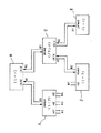
図1に、本発明の一実施例によるデータ通信システムにおけるケーブル周りの要部の構成を示す。この実施例のシステムは、IEEE1394規格に適合するものであり、従来システム(図12)と共通する構成・機能を有する部分には同一の符号を付している。
【0260】
このシステムにおいて、従来システムと相違する主要な点は、少なくとも一方のノード(装置または機器)たとえばノードAより、パワーダウンモード中にケーブル接続状態モニタ用またはウェイクアップ用のバイアス電圧VWUが出力されることである。このバイアス電圧VWUを発生するために、ノードAにはウェイクアップ・バッファ24が設けられる。
【0270】
このウェイクアップ・バッファ24はたとえばP型MOSトランジスタからなり、その出力端子(ドレイン端子)はオープンドレイン接続方式でプリント配線を介してポートTPAの片側の信号線たとえばTPA+ に接続されている。
【0280】
両ノードA,B間にケーブル10が接続され、かつノードAのウェイクアップ・バッファ24がオン状態になっていると、その出力端子よりバイアス電圧VWUがケーブル10の信号線対[L0+,L0-]を介して相手ノードBのポートTPBへ伝達され、ノードBのケーブル接続状態検出用のコンパレータ22がバイアス電圧VWUを検出するようになっている。
【0290】
図2に、ウェイクアップ・バッファ24がオン状態になっている時の電流および電位分布を等価回路で示す。なお、この等価回路では、ケーブル10[L0+,L0-]の抵抗を無視している。また、パワーダウンモード中なので、増幅器20はシャットダウン状態にあり、その出力(TPBIAS)はハイインピーダンスになっている。
【0300】
ウェイクアップ・バッファ24を構成するP型MOSトランジスタのソース端子にはたとえば3Vの電源電圧Vccが供給され、ゲート端子には制御部からのウェイクアップ制御信号WAK- が与えられる。ウェイクアップ制御信号WAK- が論理値L(たとえば0.0V)になっている時に、このP型MOSトランジスタ24はオンになる。
【0310】
一方、IEEE1394にしたがいTPBIAS用のバイアス抵抗[R0 ,R1 ]、ケーブル終端抵抗[R2 ,R3 ,R4 ]およびコンパレータ入力抵抗[R5 ,R6 ]はそれぞれ規定の抵抗値を有している。すなわち、[R0 ,R1 ]は[55Ω,55Ω]、[R2 ,R3 ,R4 ]は[55Ω,55Ω,5kΩ]、[R5 ,R6 ]は[7kΩ,7kΩ]に選ばれている。また、コンパレータ22に与えられる比較基準電圧Vs も規格で0.8Vに設定されている。
【0320】
したがって、オン状態のトランジスタ24の抵抗つまりオン抵抗をたとえば10kΩに選ぶと、そのドレイン電圧(バイアス電圧)VWUが1.005V、ドレイン電流Iが200μAになり、相手ノードBにおけるコンパレータ22の入力電圧VCNA は基準値Vs (0.8V)よりも十分に高い値(約1.002V)になる。これによって、コモンモード電圧TPBIASが検出されるときと同様に、コンパレータ22の出力CNAが論理値Lとなり、ケーブル10が接続されているというモニタ情報が得られる。
【0340】
このように、パワーダウンモード中でも、一方のノードAのウェイクアップ・バッファ24がアクティブ状態でポートTPAに所要のバイアス電圧VWUを供給することにより、両ノードA,B間にケーブル10が接続されれば、該バイアス電圧VWUがケーブル10を介して相手ノードBのポートTPBに伝達されてケーブル接続状態検出用コンパレータ22で検出される。これによって、ノードBはケーブル10が接続されていることを認識できる。
【0350】
後述するように、ノードBにウェイクアップ・バッファ24が設けられていなくても、上記のようなノードAからのウェイクアップ用バイアス電圧VWUに応動してノードBはアクティブな動作状態に切り替わり、ノードB側の増幅器20よりコモンモード電圧TPBIASを出力することができる。そして、このノードBからのコモンモード電圧TPBIASがケーブル10を介してノードAに伝達されることにより、ノードAも自己のコンパレータ22によってケーブル10が接続されていることを認識し、アクティブ動作状態に切り替わることができる。すなわち、パワーダウンモード中でも、ケーブル10が接続されたなら、両ノードA,Bが速やかにアクティブな動作状態に切り替わるようになっており、プラグ・アンド・プレイ機能が保証されている。
【0360】
本実施例によれば、ウェイクアップ・バッファ24がアクティブ状態になっている間、ケーブル10が接続されていない場合には、電源電圧端子Vccとグランドとの間で電流パスが形成されないため、電力の消費はない。なお、この時のウェイクアップ・バッファ24の出力電圧またはバイアス電圧VWUは電源電圧Vcc(3V)にほぼ等しい電圧値になっている。
【0370】
ケーブル10が接続されると、図2に示すように、電源電圧端子Vccとグランド間で各部に電流パスが形成され、各抵抗である程度の電力が消費される。しかし、ウェイクアップ・バッファ24の出力電圧(バイアス電圧)VWUは、コモンモード電圧TPBIASとは異なり、データ伝送の規格(差動駆動方式)には拘束されず、相手ノードBのコンパレータ22に検出可能な最低限の電圧値で足りる。このため、単位時間当たりの電力消費量が少ない。しかも、上記のように、ケーブル10が接続された直後に、両ノードA,Bが自動的かつ速やかにパワーダウンモードからアクティブモードに切り替わるので、ウェイクアップ機能に伴う消費電力は時間的にも非常に少ない。
【0380】
また、通常のデータ転送時には、ウェイクアップ・バッファ24がシャットダウンされるため、本来のIEEE1394規格には何の影響も与えなくて済む。
【0390】
図3に、本実施例におけるノードA内のインタフェース部の構成を示す。このインタフェース部は、フィジカル・レイヤ(物理層またはPHY)30、リンク・レイヤ(リンク層またはLINK)32およびマイクロプロセッサ(CPU)34の3個のチップから構成される。これらのチップのうち、フィジカル・レイヤ30およびリンク・レイヤ32がIEEE規格のインタフェース回路(デバイス)である。
【0400】
ウェイクアップ・バッファ24は、フィジカル・レイヤ30内に設けられ、CPU34よりウェイクアップ制御信号WAK- を受け取る。また、コモンモード電圧TPBIASを発生するための増幅器20も、フィジカル・レイヤ30内に設けられ、CPU34よりパワーダウン信号PWD- を受け取る。
【0410】
フィジカル・レイヤ30内には、IEEE1394規格にしたがい、2つの差動式トランシーバ[16a,16b]、[18a,18b]と、ケーブル接続状態検出用コンパレータ22および制御ロジック36も設けられている。相手ノードBでも、IEEE1394規格にしたがい同様のコモンモード電圧発生用増幅器20、2つの差動式トランシーバ[16a,16b]、[18a,18b]、ケーブル接続状態検出用コンパレータ22および制御ロジック36が設けられている。もちろん、ノードBも、本実施例によるウェイクアップ・バッファ24を有していてよい。
【0420】
ノードAの両トランシーバ[16a,16b]、[18a,18b]は、ケーブル10を介して襷掛けでノードBの両トランシーバ[16a,16b]、[18a,18b]と電気的に接続される。
【0430】
つまり、両ノードA,B間にケーブル10が接続されると、ノードAのポートTPAのトランシーバ[16a,16b]は第1の信号線対[L0+,L0-]を介してノードBのポートTPBのトランシーバ[18a,18b]と電気的に接続され、ノードAのポートTPBのトランシーバ[18a,18b]は第2の信号線対[L1+,L1-]を介してノードBのポートTPAのトランシーバ[16a,16b]と電気的に接続される。
【0440】
そして、データ通信時には、第1の信号線対L0+,L0-を介してノードAのポートTPAのドライバ16aからノードBのポートTPBのレシーバ18bへストローブ信号がシリアル伝送されるとともに、第2の信号線対L1+,L1-を介してノードAのポートTPBのドライバ18aからノードBのポートTPAのレシーバ16bへデータ信号がシリアル伝送される。
【0450】
一方、第2の信号線対L1+,L1-を介してノードBのポートTPBのドライバ18aからノードAのポートTPAのレシーバ16bへデータ信号がシリアル伝送されるとともに、第1の信号線対L0+,L 0-を介してノードBのポートTPAのドライバ16aからノードAのポートTPBのレシーバ18bへストローブ信号がシリアル伝送される。
【0460】
増幅器20は、CPU34からのパワーダウン信号PWD- が論理値Hレベルのときにアクティブ状態となって、差動式ライン駆動のためのコモンモード電圧TPBIAS(1.8V)を出力する。この増幅器20からのコモンモード電圧TPBIASは、バイアス抵抗R0 ,R1 を介してポートTPAの信号線TPA+ ,TPA- に印加される。上記したように、ケーブル10が接続されているときは、ノードA側からのコモンモード電圧TPBIASはケーブル10の信号線対[L0+, L0-]を介して相手ノードBのポートTPBに伝達され、ケーブル接続状態検出用のコンパレータ22によって検出される。
【0470】
パワーダウン信号PWD- が論理値Lレベルになると、増幅器20はシャットダウン状態となり、消費電力を発生しない。
【0480】
ノードAのコンパレータ22は、相手ノードBよりケーブル10の信号線対[L1+, L1-]を介してポートTPBに送られてきたコモンモード電圧TPBIASを検出する。また、相手ノードBにもウェイクアップ・バッファ24が設けられている場合、ノードAのコンパレータ22は、ノードBよりケーブル10の信号線対[L1+, L1-]を介してポートTPBに送られてきたウェイクアップ用バイアス電圧VWUをも検出することになる。コンパレータ22の出力信号CNAはCPU34に与えられる。
【0490】
コンパレータ22は、CPU34からのパワーダウン信号PWD- とは無関係に、当該ノードに電源が入っている限り継続的に動作する。また、コンパレータ22に対する比較基準電圧VS も、当該ノードに電源が入っている限り図示しない基準電圧発生器より継続的に与えられる。
【0500】
フィジカル・レイヤ30内の制御ロジック36は、両トランシーバ[16a,16b],[18a,18b]におけるドライバ/レシーバの切替制御、送信データの符号化処理、受信データの復調処理等を行うほか、後述するバス初期化のためのロジックやバス・アービトレーションのためのロジック等を有している。
【0510】
制御ロジック36は、CPU34からのパワーダウン信号PWD- が論理値Hレベルのときにアクティブな動作状態となり、パワーダウン信号PWD- が論理値Lレベルのときはパワーダウン状態またはシャットダウン状態となる。制御ロジック36がシャットダウン状態にある間は、両トランシーバ[16a,16b],[18a,18b]もシャットダウン状態に置かれる。
【0520】
リンク・レイヤ32は、フィジカル・レイヤ30とCPU34との間に介在するインタフェースであり、データ転送モードの制御、パケット処理、CRC(巡回冗長検査)生成・検査処理等を行う。リンク・レイヤ32とフィジカル・レイヤ30の制御ロジック36との間では、割込み信号LREQ、制御信号CTL 、2ビット・データdata等がやりとりされる。リンク・レイヤ32とCPU34との間では、アドレス信号ADDR、各種制御信号(チップ選択信号CS- 、書込み/読出し制御信号WR- 等)、割込み信号INT-および8ビット・データDATA等がやりとりされる。
【0530】
次に、図4〜図8につき本実施例のシステムにおいて両ノードA,Bがパワーダウンモードからバス全体を起動させるまでのシーケンスを説明する。また、図9には、比較例として、従来システムにおいて問題となる場合を示す。なお、これらの図において、記号*は当該遷移状態が発生したことを示す。
【0540】
先ず、従来システムでは、本発明によるウェイクアップ・バッファ24に相当するものがない。したがって、図9に示すように、両ノードA,Bがパワーダウンモードになっている最中に、ケーブル10が接続されても(ステート4)、両ノードA,Bのどちらもそのことに気付かず、プラグ・アンド・プレイ機能が働かない。
【0550】
これに対して、本実施例では、以下に説明するように、両ノードA,Bがパワーダウンモード中にあっても、ケーブル10が接続された時は、直ちに両ノードがアクティブノードに切り替わり、プラグ・アンド・プレイ機能が働くようになっている。しかも、消費電力の増大を招くことなく実現できる。
【0560】
本実施例において、図4の例は、ウェイクアップ・バッファ24が一方のノードAにのみ設けられており、他方のノードBには設けられていない場合である。
【0570】
図4において、初期状態では、ケーブル10が接続されておらず、かつ両ノードA,Bがパワーダウンモードになっている(ステート1)。もっとも、上記したように、パワーダウンモード中でも、各ノードA,Bにおいてフィジカル・レイヤ30内のケーブル接続状態検出用のコンパレータ22はアクティブ状態にあり、CPU34はコンパレータ22の出力CNAの状態または論理値を監視している。
【0580】
次に、ノードAのCPU34は、フィジカル・レイヤ30に対してウェイクアップ制御信号WAK- をアクティブ(論理値L)にする(ステート2)。たとえば、ノードAでデータ転送のための何らかのボタン操作が行われた時に、このウェイクアップ制御が実行されてよい。
【0590】
これにより、ノードA内では、CPU34からのウェイクアップ制御信号WAK- に応動してフィジカル・レイヤ30のウェイクアップ・バッファ24がオン状態になり、ウェイクアップ用のバイアス電圧Vwuを発生する(ステート3)。しかし、未だケーブル10が接続されていないため、ウェイクアップ・バッファ24の出力(オープンコレクタ出力)はハイインピーダンス状態になっている。したがって、このステート3の期間がいくら長く続いても、電力の消費はほとんどない。
【0600】
その後、両ノードA,B間にケーブル10が接続される(ステート4)。そうすると、ノードAのウェイクアップ・バッファ24からのバイアス電圧VWUがケーブル10の信号線対[L0+,L0-]を介して相手ノードBのポートTPBへ伝達され、ノードBのコンパレータ22がバイアス電圧VWUまたはVCNA を検出する(ステート5)。
【0610】
次いで、ノードB内では、CPU34がコンパレータ22の出力(論理値LのCNA)を認識する(ステート6)。これによって、ノードBは起動シーケンスに入り、CPU34がフィジカル・レイヤ30およびリンク・レイヤ32をアクティブ状態に切り替える(ステート7)。すなわち、フィジカル・レイヤ30に対してはパワーダウン信号PWD- を非アクティブ(論理値H)に切り替え、リンク・レイヤ32に対しては所定の制御信号たとえばチップ選択信号CS- をアクティブ(論理値L)にする。
【0620】
これにより、ノードB内では、3つのチップ30,32,34が全てアクティブな動作状態になり(ステート8)、フィジカル・レイヤ30の増幅器20よりコモンモード電圧TPBIASが発生される。
【0630】
ノードBからのコモンモード電圧TPBIASは、ケーブル10の信号線対[L1+,L1-]を介してノードAのポートTPBに伝えられ、ノードAのコンパレータ22にバイアス電圧VCNA として検出される(ステート9)。
【0640】
次いで、ノードA内では、CPU34がコンパレータ22の出力(論理値LのCNA)を認識する(ステート10)。これによって、ノードAも起動シーケンスに入り、CPU34がフィジカル・レイヤ30およびリンク・レイヤ32をアクティブ状態に切り替える(ステート11)。
【0650】
この際、フィジカル・レイヤ30に対しては、パワーダウン信号PWD- が非アクティブ(論理値H)に切り替わるのと同時に(入れ代わりに)、ウェイクアップ信号WAK- が非アクティブ(論理値H)に切り替わる。これによって、ウェイクアップ・バッファ24はオフ状態になる。
【0660】
こうして、両ノードA,B間でケーブル10が接続され、かつ各ノードのインタフェース部がオン状態になったことで、バス・リセットが行われ、それぞれのフィジカル・レイヤ30,30の間でIEEE1394規格に基づいた所定の手順でバス初期化が実行される(ステート12)。
【0670】
このように、この例では、ノードBにウェイクアップ・バッファ24が設けられていなくても、ケーブル10が接続された時点で、ノードAからのウェイクアップ用バイアス電圧VWUに応動してノードBがパワーダウンモードからアクティブモードに切り替わることができる。そして、このアクティブ状態になったノードBの起動シーケンスを利用することで、ノードAもパワーダウンモードからアクティブモードに切り替わることができ、バス全体の起動が速やかに行われる。
【0680】
図5の例は、ケーブル10が最初から接続されている場合であり、他の条件は図4の例と同じである。この場合は、ノードAでウェイクアップ・バッファ24が作動するや否や、そのウェイクアップ用バイアス電圧VWUがケーブル10を介して相手ノードBに伝達され、ノードBのコンパレータ22に検出される。したがって、ノードAでウェイクアップを開始してからノードBがそれに気付くまでの待ち時間(ステート4)が実質的に省かれる。それ以外の動作は図4の例と同じである。
【0690】
図6の例は、両ノードA,Bの双方にウェイクアップ・バッファ24が設けられている場合である。この場合は、パワーダウンモード中に両ノードA,Bがそれぞれのウェイクアップ・バッファ24をオン状態にする(ステート2,3)。この間、ケーブル10が未接続でも、各ノードでウェイクアップ・バッファ24が電力を消費することはない。そして、ケーブル10が接続されると(ステート4)、両ノードA,Bは互いに相手ノードからのバイアス電圧VWUを検出して(ステート5,6)、同時または並列的にアクティブ状態に切り替わり(ステート7,8)、直ちにバス初期化を開始することができる(ステート12)。
【0700】
なお、最初からケーブル10が接続されている場合で、両ノードA,Bがほぼ同時にそれぞれのウェイクアップ・バッファ24をオンにしたときは、ケーブル接続までの待機時間(ステート3)が省かれる。それ以外は、図6と同様の動作が行われる。また、パワーダウンモード中に両ノードA,Bの一方が先にウェイクアップ・バッファ24をオンにしたときは、図4または図5と同様の動作が行われる。
【0710】
図7は、上記した図4の例でノードBに他のノードCが別のケーブルを介して接続されている場合である。ノードAの動作は、図7では省略しているが、図4と同じである。
【0720】
この場合、ノードBは、IEEE1394対応の2つのポート#1,#2を有し、ポート#1でノードAと接続され、ポート#2でノードCに接続される。各ポート#1,#2には個別のフィジカル・レイヤ30が充てられ、各フィジカル・レイヤ30は独立して動作する。しかし、いずれかのポート(図7では#1)が他のノード(A)とつながると、全てのポート(#1,#2)で一斉にバス初期化が行われる(ステート12)。
【0730】
IEEE1394規格では、デイジチェーン方式またはノード分岐方式により同一のネットワーク上に多数のノードを接続することが可能であり、いずれかのノードでケーブルの抜き差しが行われる度にバス・リセットないしバス初期化が行われ、新たなネットワーク・トポロジが構築される。
【0740】
図8に、IEEE1394におけるネットワーク・トポロジの一例を示す。図8において、ケーブル接続されたポート#を1本しか持たないノードA,D,Eは、それぞれがネットワークの端にあるノード(リーフ)であることを認識し、その接続先つまり親(parent)であるノードB,Cに対して問い合わせを行う。そうすると、ノードB,Cは、その問い合わせを受けた自己のポート#1,(#2,#3)で親子関係を確認すると同時に、それ以外にケーブル接続されている他のポート#2,#1から接続先のノード(C,B)に対してさらに問い合わせを行う。こうして順次親子関係が決まっていく。
【0750】
この例では、ノードB,Cが互いに問い合わせを出し合う。この場合は、両ノードB,C間でルートを決定するためのやりとりが所定の手順で行われる。その結果、図8の例では、ノードBがルートとなり、ノードCがブランチになる。ルート(ノードB)は、ネットワークの中心となり、バス・アービトレーションの判定等を行う。
【0760】
以上好適な実施例について説明したが、本発明の技術思想の範囲内で種々の変形・変更が可能である。
【0770】
たとえば、上記した実施例では、ウェイクアップ・バッファ24の出力端子をデバイス(フィジカル・レイヤ30)の外のプリント基板上でポートTPA+ に接続した。しかし、この配線は一例であり、たとえば図10に示すように、デバイスの内部で配線を行ってもよい。また、ウェイクアップ・バッファ24の出力端子を他方のポートTPA- に接続しても同様の作用効果が得られる。ウェイクアップ・バッファ24の構成も種々の変形が可能であり、たとえばユニポーラ・トランジスタで構成することもできる。
【0780】
また、他の回路要素も種々の変形が可能である。たとえば、上記実施例では、コモンモード電圧発生用の増幅器20は個別の回路として構成されている。しかし、この増幅器20と同等の機能を有する増幅回路をドライバ16a,18aに内蔵させることも可能である。
【0790】
上記した実施例はIEEE1394規格に適合するシステムに係るものであったが、本発明の一適用例であり、本発明はコモンモード電圧を必要とする任意の差動駆動式データ通信システムに適用可能である。
【0800】
【発明の効果】
以上説明したように、本発明によれば、パワーダウンモード中に電力消費を抑えながらケーブル接続状態を直ちに検出することが可能である。したがって、マルチメディア・システムにおいて効率的かつ確実なプラグ・アンド・プレイ機能を保証することができる。
【図面の簡単な説明】
【図1】本発明の一実施例によるデータ通信システムにおけるケーブル周りの要部の構成を示す回路図である。
【図2】実施例のシステムでウエイクアップ・バッファがオン状態になっている時の電流および電位分布を等価回路で示す回路図である。
【図3】実施例におけるノード内のインタフェース部の構成を示すブロック図である。
【図4】実施例において2つのノードがパワーダウンモードからバス全体を起動させるまでのシーケンスの一例を示す図である。
【図5】実施例において2つのノードがパワーダウンモードからバス全体を起動させるまでのシーケンスの別の例を示す図である。
【図6】実施例において2つのノードがパワーダウンモードからバス全体を起動させるまでのシーケンスの別の例を示す図である。
【図7】図4の例において一方のノードに第3のノードが接続されている場合のシーケンスを例を示す図である。
【図8】IEEE1394規格におけるネットワーク・トポロジの一例を示すブロック図である。
【図9】実施例におけるシーケンスの比較例として従来システムにおいて問題となる場合を示す図である。
【図10】実施例におけるウェイクアップ・バッファの出力の配線の変形例を示す要部の回路図である。
【図11】IEEE1394規格で採用するDS−Link符号化方式を説明するための信号波形図である。
【図12】IEEE1394規格にしたがう従来のデータ通信システムにおけるケーブル周りの要部の構成を示す回路図である。
【符号の説明】
A,B ノード
10 ケーブル
16a,18a ドライバ
16b,18b レシーバ
20 コモンモード電圧発生用増幅器
22 ケーブル接続状態検出用コンパレータ
24 ウェイクアップ・バッファ
30 フィジカル・レイヤ
32 リンク・レイヤ
34 CPU[0010]
BACKGROUND OF THE INVENTION
The present invention relates to a data communication system that transmits signals by driving both signal lines in a differential manner while applying a predetermined common bias voltage to a pair of signal lines between two devices.
[0020]
[Prior art]
An example of this type of data communication system is an interface defined as IEEE 1394. This IEEE1394 is a peripheral device interface standard for personal computers for multimedia, and three types of data transfer speeds of 100 Mbps, 200 Mbps, and 400 Mbps are possible on the same network, and data transfer between peripheral devices is also possible. ing.
[0030]
In IEEE 1394, a serial bus is constructed on a cable composed of two pairs of signal lines, and data is transmitted by the DS-Link encoding method. Here, as shown in FIG. 11, the DS-Link encoding method sends a data signal on one signal line from the transmission side and simultaneously sends a strobe signal on another signal line from the transmission side. This is a method of reproducing the clock signal for synchronization by taking the exclusive OR of both signals. This method has advantages in that the transmission efficiency is higher than that of a general serial transfer format using start bits and stop bits, and the clock frequency or data transfer rate can be improved because the skew margin is large.
[0040]
FIG. 12 shows a configuration of a main part around a cable in a conventional data communication system based on the IEEE 1394 standard. Two signal line pairs [L0 +, L0-] and [L1 +, L1-] of the
[0050]
Each node A, B is provided with two sets of ports TPA, TPB. The port TPA of the own node is electrically connected to the port TPB of the partner node in a hanging manner, and the port TPB of the own node is connected to the partner node. Electrically connected to port TPA.
[0060]
More specifically, a strobe signal is transmitted from the
[0070]
On the other hand, a strobe signal is transmitted from the driver (not shown) of the port TPA of the node B to the receiver (not shown) of the port TPB of the node A via the second signal line pair L1 +, L1- A data signal is transmitted from a driver (not shown) of the port B of the node B to a receiver (not shown) of the port TPA of the node A via one signal line pair L0 +, L0-.
[0080]
In the port TPA of each node A and B, the common mode voltage TPBIAS having a constant voltage value (for example, 1.8 V) based on the differential drive method of the DS-Link encoding system is resistance by the
[0090]
On the other hand, at the ports TPB of the nodes A and B, the
[0100]
In this way, each of the nodes A and B detects whether or not the
[0110]
[Problems to be solved by the invention]
By the way, among the devices incorporating the IEEE1394 interface, in a battery-driven application such as a digital camera, the interface circuit (device) of this standard is usually set in a power-down mode while data is not transferred in order to reduce power consumption. Is set. During the power down mode, most of the circuits (particularly the
[0120]
Therefore, when both the nodes A and B are in the power down mode when the user connects the
[0130]
In order to avoid this problem, if the
[0140]
The present invention has been made in view of the above-described problems, and an object of the present invention is to provide a data communication system that can immediately detect a cable connection state while suppressing power consumption during a power-down mode.
[0150]
It is another object of the present invention to provide a data communication system that can guarantee an efficient and reliable plug and play function in a multimedia system.
[0160]
[Means for Solving the Problems]
In order to achieve the above object, in the data communication system according to
[0170]
According to a second aspect of the present invention, there is provided the data communication system according to the first aspect, wherein the first and second signal line pairs are detachably connected between the first and second devices. For the first signal line pair, the first device is provided with the first and second bias generating means, the second device is provided with the bias detecting means, and the second signal line pair is provided with the first signal line pair. In the second apparatus, the first bias generating means is provided, and the bias detecting means is provided in the first apparatus.
[0180]
The system activation method according to
[0190]
The system activation method according to
[0200]
According to a fifth aspect of the present invention, there is provided the data communication system according to the first aspect, wherein the first and second signal line pairs are detachably connected between the first and second devices. For the first signal line pair, the first device is provided with the first and second bias generating means, the second device is provided with the bias detecting means, and the second signal line pair is provided with the first signal line pair. In the second apparatus, the first and second bias generating means are provided, and the bias detecting means is provided in the first apparatus.
[0210]
The system activation method according to
[0220]
The system activation method according to
[0230]
Further, in the data communication system according to
[0240]
DETAILED DESCRIPTION OF THE INVENTION
Embodiments of the present invention will be described below with reference to FIGS.
[0250]
FIG. 1 shows a configuration of a main part around a cable in a data communication system according to an embodiment of the present invention. The system of this embodiment conforms to the IEEE 1394 standard, and portions having the same configuration and function as those of the conventional system (FIG. 12) are denoted by the same reference numerals.
[0260]
In this system, the main difference from the conventional system is that a bias voltage VWU for monitoring the cable connection state or for wakeup is output from at least one node (device or equipment), for example, node A, during the power down mode. That is. In order to generate the bias voltage VWU, a
[0270]
The wake-up
[0280]
When the
[0290]
FIG. 2 shows an equivalent circuit of current and potential distribution when the wake-up
[0300]
For example, a power supply voltage Vcc of 3V is supplied to the source terminal of the P-type MOS transistor constituting the
[0310]
On the other hand, the bias resistors [R0, R1] for TPBIAS, the cable termination resistors [R2, R3, R4] and the comparator input resistors [R5, R6] according to IEEE 1394 have specified resistance values, respectively. That is, [R0, R1] is selected as [55Ω, 55Ω], [R2, R3, R4] is selected as [55Ω, 55Ω, 5kΩ], and [R5, R6] is selected as [7kΩ, 7kΩ]. Further, the comparison reference voltage Vs given to the
[0320]
Therefore, if the resistance of the
[0340]
Thus, even in the power down mode, the
[0350]
As will be described later, even if the
[0360]
According to the present embodiment, when the
[0370]
When the
[0380]
Further, during normal data transfer, the
[0390]
FIG. 3 shows the configuration of the interface unit in the node A in this embodiment. This interface unit is composed of three chips: a physical layer (physical layer or PHY) 30, a link layer (link layer or LINK) 32, and a microprocessor (CPU) 34. Of these chips, the
[0400]
The wake-up
[0410]
In the
[0420]
Both transceivers [16a, 16b] and [18a, 18b] of the node A are electrically connected to both transceivers [16a, 16b] and [18a, 18b] of the node B through the
[0430]
That is, when the
[0440]
At the time of data communication, a strobe signal is serially transmitted from the
[0450]
On the other hand, a data signal is serially transmitted from the
[0460]
The
[0470]
Power down signal PWD- Becomes a logic L level, the
[0480]
The
[0490]
The
[0500]
The
[0510]
The
[0520]
The
[0530]
Next, with reference to FIGS. 4 to 8, the sequence from the power-down mode until both nodes A and B activate the entire bus in the system of this embodiment will be described. FIG. 9 shows, as a comparative example, a problem in the conventional system. In these figures, the symbol * indicates that the transition state has occurred.
[0540]
First, the conventional system has nothing equivalent to the wake-up
[0550]
In contrast, in this embodiment, as described below, even when both nodes A and B are in the power down mode, when the
[0560]
In the present embodiment, the example of FIG. 4 is a case where the wake-up
[0570]
In FIG. 4, in the initial state, the
[0580]
Next, the
[0590]
Thus, in node A, the wake-up control signal WAK from the
[0600]
Thereafter, the
[0610]
Next, in the node B, the
[0620]
As a result, in the node B, all the three
[0630]
The common mode voltage TPBIAS from the node B is transmitted to the port TPB of the node A through the signal line pair [L1 +, L1-] of the
[0640]
Next, in the node A, the
[0650]
At this time, for the
[0660]
In this way, the
[0670]
Thus, in this example, even if the
[0680]
The example of FIG. 5 is a case where the
[0690]
The example of FIG. 6 is a case where the wake-up
[0700]
In the case where the
[0710]
FIG. 7 shows a case where another node C is connected to the node B via another cable in the example of FIG. 4 described above. The operation of the node A is omitted in FIG. 7, but is the same as that in FIG.
[0720]
In this case, the node B has two
[0730]
According to the IEEE 1394 standard, a large number of nodes can be connected to the same network by a daisy chain method or a node branch method, and a bus reset or a bus initialization is performed each time a cable is connected or disconnected at any node. And a new network topology is built.
[0740]
FIG. 8 shows an example of a network topology in IEEE 1394. In FIG. 8, nodes A, D, and E having only one port # connected by a cable recognize that each node is a node (leaf) at the end of the network, and their connection destination, that is, a parent. An inquiry is made to nodes B and C. Then, the nodes B and C confirm the parent-child relationship with their
[0750]
In this example, nodes B and C make inquiries with each other. In this case, exchange for determining a route between both nodes B and C is performed in a predetermined procedure. As a result, in the example of FIG. 8, node B becomes the root and node C becomes the branch. The route (node B) is the center of the network and performs bus arbitration determination and the like.
[0760]
The preferred embodiments have been described above, but various modifications and changes can be made within the scope of the technical idea of the present invention.
[0770]
For example, in the above embodiment, the output terminal of the wake-up
[0780]
Also, other circuit elements can be variously modified. For example, in the above embodiment, the common mode
[0790]
The embodiment described above relates to a system conforming to the IEEE 1394 standard, but is an application example of the present invention, and the present invention can be applied to any differential drive type data communication system that requires a common mode voltage. It is.
[0800]
【The invention's effect】
As described above, according to the present invention, it is possible to immediately detect the cable connection state while suppressing power consumption during the power down mode. Therefore, an efficient and reliable plug and play function can be ensured in the multimedia system.
[Brief description of the drawings]
FIG. 1 is a circuit diagram showing a configuration of a main part around a cable in a data communication system according to an embodiment of the present invention.
FIG. 2 is a circuit diagram showing current and potential distribution in an equivalent circuit when a wakeup buffer is in an on state in the system of the embodiment.
FIG. 3 is a block diagram illustrating a configuration of an interface unit in a node according to the embodiment.
FIG. 4 is a diagram illustrating an example of a sequence in which two nodes start up the entire bus from a power down mode in the embodiment.
FIG. 5 is a diagram illustrating another example of a sequence until two nodes start up the entire bus from the power-down mode in the embodiment.
FIG. 6 is a diagram illustrating another example of a sequence from when the two nodes start up the entire bus from the power-down mode in the embodiment.
7 is a diagram illustrating an example of a sequence when a third node is connected to one node in the example of FIG. 4;
FIG. 8 is a block diagram illustrating an example of a network topology in the IEEE 1394 standard.
FIG. 9 is a diagram showing a case where there is a problem in a conventional system as a sequence comparison example in the embodiment.
FIG. 10 is a circuit diagram of a main part showing a modification of the output wiring of the wakeup buffer in the embodiment.
FIG. 11 is a signal waveform diagram for explaining a DS-Link encoding method employed in the IEEE 1394 standard.
FIG. 12 is a circuit diagram showing a configuration of a main part around a cable in a conventional data communication system according to the IEEE 1394 standard.
[Explanation of symbols]
A and B nodes
10 cables
16a, 18a driver
16b, 18b receiver
20 Common mode voltage generating amplifier
22 Comparator for cable connection status detection
24 Wake-up buffer
30 Physical Layer
32 Link layer
34 CPU
Claims (8)
各々の前記装置は前記一対の信号線を差動式で駆動することによって信号を相手側の前記装置に送信し、
前記第1の装置には、アクティブモード中に前記一対の信号線に共通に印加するための前記差動式駆動法に応じた第1のバイアス電圧を発生し、かつパワーダウンモード中は前記第1のバイアス電圧の発生を止める第1のバイアス発生手段と、パワーダウンモード中に前記一対の信号線の片方に印加するための前記差動式駆動法に依存しない第2のバイアス電圧を発生し、かつアクティブモード中に前記第2のバイアス電圧の発生を止める第2のバイアス発生手段とが設けられ、
前記第2の装置には、前記信号線上に前記第1または第2のバイアス電圧が印加されているか否かを検出するためのバイアス検出手段が設けられているデータ通信システム。At least a pair of signal lines are detachably connected between the first and second devices,
Each of the devices transmits a signal to the counterpart device by driving the pair of signal lines differentially,
The first device generates a first bias voltage according to the differential driving method for commonly applying to the pair of signal lines during the active mode, and the first device during the power down mode. First bias generating means for stopping the generation of one bias voltage, and a second bias voltage independent of the differential driving method for applying to one of the pair of signal lines during the power down mode. And a second bias generating means for stopping the generation of the second bias voltage during the active mode,
A data communication system, wherein the second device is provided with bias detection means for detecting whether or not the first or second bias voltage is applied to the signal line.
前記第1および第2の装置が共にパワーダウンモード中で、かつ両装置間に前記第1および第2の信号線対が接続されていない時に前記第1の装置側で前記第2のバイアス発生手段より前記第2のバイアス電圧の発生を開始する第1のステップと、
前記第1のステップの後に、前記第1および第2の装置間における前記第1および第2の信号線対の接続に応答して、前記第2の装置側で前記バイアス検出手段により前記第1の対の信号線を介して前記第2のバイアス電圧を検出する第2のステップと、
前記第2のステップの直後に前記第2の装置側がアクティブモードになって前記第1のバイアス電圧発生手段より前記第2の信号線対に対して前記第1のバイアス電圧の発生を開始する第3のステップと、
前記第3のステップの直後に前記第1の装置側で前記バイアス検出手段により前記第2の信号線対を介して前記第1のバイアス電圧を検出する第4のステップと、
前記第4のステップの直後に前記第1の装置側がアクティブモードになる第5のステップと、
前記第5のステップの直後に前記第1および第2の装置間で初期化のためのデータ通信を行う第6のステップと
を有するシステム起動方法。In the system starting method in the data communication system according to claim 2,
Generation of the second bias on the first device side when the first and second devices are both in power-down mode and the first and second signal line pairs are not connected between the devices. A first step of starting the generation of the second bias voltage by means;
After said first step, said response to said first and second signal line pairs of the connection between the first and second devices, said by the bias detecting means at the second device side first A second step of detecting the second bias voltage via a pair of signal lines;
Immediately after the second step, the second device side enters an active mode, and the first bias voltage generating means starts generating the first bias voltage to the second signal line pair from the first bias voltage generating means. 3 steps,
A fourth step of detecting said first bias voltage via said second signal line pair by the bias detecting means at the first device side immediately after the third step,
The first device side and a fifth step comprising the active mode immediately after the fourth step,
And a sixth step of performing data communication for initialization between the first and second devices immediately after the fifth step.
前記第1および第2の装置が共にパワーダウンモード中で、かつ両装置間に前記第1および第2の信号線が接続されている時に前記第1の装置側で前記第2のバイアス発生手段より前記第2のバイアス電圧の発生を開始する第1のステップと、
前記第1のステップの後に前記第2の装置で前記バイアス検出手段により前記第1の信号線対を介して前記第2のバイアス電圧を検出する第2のステップと、
前記第2のステップの直後に前記第2の装置側がアクティブモードになって前記第1のバイアス電圧発生手段より前記第2の信号線対に対して前記第1のバイアス電圧の発生を開始する第3のステップと、
前記第3のステップの直後に前記第1の装置側で前記バイアス検出手段により前記第2の信号線対を介して前記第1のバイアス電圧を検出する第4のステップと、
前記第4のステップの直後に前記第1の装置側がアクティブモードになる第5のステップと、
前記第5のステップの直後に前記第1および第2の装置間で初期化のためのデータ通信を行う第6のステップと
を有するシステム起動方法。In the system starting method in the data communication system according to claim 2,
When the first and second devices are both in a power down mode and the first and second signal lines are connected between the two devices, the second bias generating means is provided on the first device side. A first step of starting the generation of the second bias voltage;
A second step of detecting the second bias voltage via the first signal line pair by the bias detection means in the second device after the first step;
Immediately after the second step, the second device side enters an active mode, and the first bias voltage generating means starts generating the first bias voltage to the second signal line pair from the first bias voltage generating means. 3 steps,
A fourth step of detecting the first bias voltage via the second signal line pair by the bias detection means on the first device side immediately after the third step;
A fifth step in which the first device enters the active mode immediately after the fourth step;
And a sixth step of performing data communication for initialization between the first and second devices immediately after the fifth step.
前記第1および第2の装置が共にパワーダウンモード中で、かつ両装置間に前記第1および第2の信号線が接続されていない時に前記第1の装置側で前記第2のバイアス発生手段より前記第2のバイアス電圧の発生を開始する第1のステップと、
前記第1のステップの後に、前記第1および第2の装置間における前記第1および第2の信号線対の接続に応答して、前記第2の装置側で前記バイアス検出手段により前記第1の信号線対を介して前記第2のバイアス電圧を検出するとともに前記第1の装置側で前記バイアス検出手段により前記第2の信号線対を介して前記第2のバイアス電圧を検出する第2のステップと、
前記第2のステップの直後に前記第1および第2の装置がそれぞれアクティブモードになる第3のステップと、
前記第3のステップの直後に前記第1および第2の装置間で初期化のためのデータ通信を行う第4のステップと
を有するシステム起動方法。The system activation method in the data communication system according to claim 5,
When the first and second devices are both in a power down mode and the first and second signal lines are not connected between the two devices, the second bias generating means is provided on the first device side. A first step of starting the generation of the second bias voltage;
After said first step, said response to said first and second signal line pairs of the connection between the first and second devices, said by the bias detecting means at the second device side first The second bias voltage is detected via one signal line pair, and the second bias voltage is detected via the second signal line pair by the bias detection means on the first apparatus side. Two steps,
A third step consisting in active mode wherein immediately after the second step the first and second devices respectively,
And a fourth step of performing data communication for initialization between the first and second devices immediately after the third step.
前記第1および第2の装置が共にパワーダウンモード中で、かつ両装置間に前記第1および第2の信号線対が接続されている時に両装置側でそれぞれ前記第2のバイアス発生手段より前記第2のバイアス電圧の発生を開始する第1のステップと、
前記第1のステップの直後に前記第2の装置側で前記バイアス検出手段により前記第1の信号線対を介して前記第2のバイアス電圧を検出するとともに前記第1の装置側で前記バイアス検出手段により前記第2の信号線対を介して前記第2のバイアス電圧を検出する第2のステップと、
前記第2のステップの直後に前記第1および第2の装置がそれぞれアクティブモードになる第3のステップと、
前記第3のステップの直後に前記第1および第2の装置間で初期化のためのデータ通信を行う第4のステップと
を有するシステム起動方法。The system activation method in the data communication system according to claim 5,
When both the first and second devices are in the power-down mode and the first and second signal line pairs are connected between the two devices, the second bias generating means on each device side respectively. A first step for starting generation of the second bias voltage;
Immediately after the first step, the bias detection means detects the second bias voltage via the first signal line pair on the second device side and detects the bias on the first device side. A second step of detecting the second bias voltage via the second signal line pair by means;
A third step in which the first and second devices are each in an active mode immediately after the second step;
And a fourth step of performing data communication for initialization between the first and second devices immediately after the third step.
Priority Applications (1)
| Application Number | Priority Date | Filing Date | Title |
|---|---|---|---|
| JP21580697A JP3987163B2 (en) | 1997-07-25 | 1997-07-25 | Data communication system |
Applications Claiming Priority (1)
| Application Number | Priority Date | Filing Date | Title |
|---|---|---|---|
| JP21580697A JP3987163B2 (en) | 1997-07-25 | 1997-07-25 | Data communication system |
Publications (2)
| Publication Number | Publication Date |
|---|---|
| JPH1145130A JPH1145130A (en) | 1999-02-16 |
| JP3987163B2 true JP3987163B2 (en) | 2007-10-03 |
Family
ID=16678573
Family Applications (1)
| Application Number | Title | Priority Date | Filing Date |
|---|---|---|---|
| JP21580697A Expired - Lifetime JP3987163B2 (en) | 1997-07-25 | 1997-07-25 | Data communication system |
Country Status (1)
| Country | Link |
|---|---|
| JP (1) | JP3987163B2 (en) |
Families Citing this family (10)
| Publication number | Priority date | Publication date | Assignee | Title |
|---|---|---|---|---|
| JP3498944B2 (en) | 1999-08-30 | 2004-02-23 | Necエレクトロニクス株式会社 | Input buffer circuit with cable detection function |
| JP3933643B2 (en) * | 2004-03-31 | 2007-06-20 | 山洋電気株式会社 | Abnormal transmission method using differential transmission circuit |
| JP4625712B2 (en) | 2005-04-14 | 2011-02-02 | パナソニック株式会社 | Semiconductor integrated circuit and electronic equipment |
| JP4939339B2 (en) * | 2007-08-20 | 2012-05-23 | ルネサスエレクトロニクス株式会社 | Differential transmission circuit, differential reception circuit, signal transmission circuit and signal transmission system |
| JP2010206268A (en) * | 2009-02-27 | 2010-09-16 | Denso Corp | Communication system and node |
| JP2013042195A (en) * | 2009-12-15 | 2013-02-28 | Panasonic Corp | Interface circuit |
| DE102012201651A1 (en) * | 2012-02-03 | 2013-08-08 | Dr. Johannes Heidenhain Gmbh | Position measuring device |
| JP5803895B2 (en) * | 2012-12-26 | 2015-11-04 | 株式会社デンソー | Transmission equipment |
| JP2015065598A (en) * | 2013-09-25 | 2015-04-09 | 日本電気株式会社 | Cable connection transceiver, transmitter, receiver, cable connection support method and cable connection support program |
| WO2016079798A1 (en) | 2014-11-18 | 2016-05-26 | 株式会社ソシオネクスト | Clock transmission circuit and semiconductor integrated circuit |
-
1997
- 1997-07-25 JP JP21580697A patent/JP3987163B2/en not_active Expired - Lifetime
Also Published As
| Publication number | Publication date |
|---|---|
| JPH1145130A (en) | 1999-02-16 |
Similar Documents
| Publication | Publication Date | Title |
|---|---|---|
| US11561920B2 (en) | Interface for bridging out-of-band information from a downstream communication link to an upstream communication link | |
| KR100514262B1 (en) | Electronic apparatus and operation mode controlling method therefor | |
| US20020169915A1 (en) | USB connection-detection circuitry and operation methods of the same | |
| US7805621B2 (en) | Method and apparatus for providing a bus interface with power management features | |
| JP2020074102A (en) | Power-saving mode for usb power transfer sourcing device | |
| EP0900493B1 (en) | Communication bus using different transmission rates | |
| JP3544932B2 (en) | Electronic device and power control method thereof | |
| US6754692B2 (en) | Configurable power distribution circuit | |
| KR101845095B1 (en) | Efficient entry into and recovery from a power save mode for a differential transmitter and receiver | |
| US6625738B1 (en) | USB apparatus that turns on computer power supply using signals substantially longer than information conveying pulse widths when predetermined operation is performed on input device | |
| JP3610424B2 (en) | Electronic equipment and interface circuit | |
| JP3745162B2 (en) | Link control state machine | |
| US20040148451A1 (en) | USB controlling apparatus for data transfer between computers and method for the same | |
| US7689852B2 (en) | Method and system for providing power management for an integrated gigabit ethernet controller | |
| JP2002341982A (en) | Universal serial bus circuit | |
| JP3987163B2 (en) | Data communication system | |
| US6477605B1 (en) | Apparatus and method for controlling device connection | |
| JPH11355321A (en) | Medium access controller | |
| US20020172151A1 (en) | Transmission circuit, data transfer control device, and electronic equipment | |
| JP2012508491A (en) | Circuit configuration including transceiver circuit for bus system, and node for bus system | |
| JP3599048B2 (en) | Data transfer control system, electronic device, program, and data transfer control method | |
| US20060050731A1 (en) | High-speed IEEE 1394 link interface | |
| JPH10233793A (en) | Information transmitting system | |
| JP2002073219A (en) | Interface device equipped with part for supplying power to external device and method for supplying power to external device | |
| US8285885B2 (en) | Universal serial bus device and universal serial bus system |
Legal Events
| Date | Code | Title | Description |
|---|---|---|---|
| A521 | Written amendment |
Free format text: JAPANESE INTERMEDIATE CODE: A523 Effective date: 20040708 |
|
| A621 | Written request for application examination |
Free format text: JAPANESE INTERMEDIATE CODE: A621 Effective date: 20040708 |
|
| A977 | Report on retrieval |
Free format text: JAPANESE INTERMEDIATE CODE: A971007 Effective date: 20061222 |
|
| A131 | Notification of reasons for refusal |
Free format text: JAPANESE INTERMEDIATE CODE: A131 Effective date: 20070327 |
|
| A521 | Written amendment |
Free format text: JAPANESE INTERMEDIATE CODE: A523 Effective date: 20070524 |
|
| TRDD | Decision of grant or rejection written | ||
| A01 | Written decision to grant a patent or to grant a registration (utility model) |
Free format text: JAPANESE INTERMEDIATE CODE: A01 Effective date: 20070710 |
|
| A61 | First payment of annual fees (during grant procedure) |
Free format text: JAPANESE INTERMEDIATE CODE: A61 Effective date: 20070712 |
|
| R150 | Certificate of patent or registration of utility model |
Free format text: JAPANESE INTERMEDIATE CODE: R150 |
|
| FPAY | Renewal fee payment (event date is renewal date of database) |
Free format text: PAYMENT UNTIL: 20100720 Year of fee payment: 3 |
|
| FPAY | Renewal fee payment (event date is renewal date of database) |
Free format text: PAYMENT UNTIL: 20110720 Year of fee payment: 4 |
|
| FPAY | Renewal fee payment (event date is renewal date of database) |
Free format text: PAYMENT UNTIL: 20110720 Year of fee payment: 4 |
|
| FPAY | Renewal fee payment (event date is renewal date of database) |
Free format text: PAYMENT UNTIL: 20120720 Year of fee payment: 5 |
|
| FPAY | Renewal fee payment (event date is renewal date of database) |
Free format text: PAYMENT UNTIL: 20120720 Year of fee payment: 5 |
|
| FPAY | Renewal fee payment (event date is renewal date of database) |
Free format text: PAYMENT UNTIL: 20130720 Year of fee payment: 6 |
|
| R250 | Receipt of annual fees |
Free format text: JAPANESE INTERMEDIATE CODE: R250 |
|
| R250 | Receipt of annual fees |
Free format text: JAPANESE INTERMEDIATE CODE: R250 |
|
| R250 | Receipt of annual fees |
Free format text: JAPANESE INTERMEDIATE CODE: R250 |
|
| R250 | Receipt of annual fees |
Free format text: JAPANESE INTERMEDIATE CODE: R250 |
|
| R250 | Receipt of annual fees |
Free format text: JAPANESE INTERMEDIATE CODE: R250 |
|
| EXPY | Cancellation because of completion of term |