JP3980361B2 - Two-step trench etching to form a fully integrated thermal inkjet printhead - Google Patents
Two-step trench etching to form a fully integrated thermal inkjet printhead Download PDFInfo
- Publication number
- JP3980361B2 JP3980361B2 JP2002016080A JP2002016080A JP3980361B2 JP 3980361 B2 JP3980361 B2 JP 3980361B2 JP 2002016080 A JP2002016080 A JP 2002016080A JP 2002016080 A JP2002016080 A JP 2002016080A JP 3980361 B2 JP3980361 B2 JP 3980361B2
- Authority
- JP
- Japan
- Prior art keywords
- ink supply
- layer
- substrate
- forming
- thin film
- Prior art date
- Legal status (The legal status is an assumption and is not a legal conclusion. Google has not performed a legal analysis and makes no representation as to the accuracy of the status listed.)
- Expired - Fee Related
Links
- 238000005530 etching Methods 0.000 title claims description 48
- 239000010410 layer Substances 0.000 claims description 143
- 238000000034 method Methods 0.000 claims description 68
- 239000010409 thin film Substances 0.000 claims description 64
- 239000000758 substrate Substances 0.000 claims description 63
- 239000011241 protective layer Substances 0.000 claims description 58
- WGTYBPLFGIVFAS-UHFFFAOYSA-M tetramethylammonium hydroxide Chemical compound [OH-].C[N+](C)(C)C WGTYBPLFGIVFAS-UHFFFAOYSA-M 0.000 claims description 24
- 230000000873 masking effect Effects 0.000 claims description 8
- 238000007639 printing Methods 0.000 claims description 8
- 238000000151 deposition Methods 0.000 claims description 6
- BOTDANWDWHJENH-UHFFFAOYSA-N Tetraethyl orthosilicate Chemical compound CCO[Si](OCC)(OCC)OCC BOTDANWDWHJENH-UHFFFAOYSA-N 0.000 claims description 5
- 238000004519 manufacturing process Methods 0.000 description 14
- 230000008569 process Effects 0.000 description 11
- XUIMIQQOPSSXEZ-UHFFFAOYSA-N Silicon Chemical compound [Si] XUIMIQQOPSSXEZ-UHFFFAOYSA-N 0.000 description 9
- 239000004020 conductor Substances 0.000 description 9
- 229910052710 silicon Inorganic materials 0.000 description 9
- 239000010703 silicon Substances 0.000 description 9
- 230000004048 modification Effects 0.000 description 7
- 238000012986 modification Methods 0.000 description 7
- 238000007796 conventional method Methods 0.000 description 6
- 239000010408 film Substances 0.000 description 6
- 238000013461 design Methods 0.000 description 5
- 229910016570 AlCu Inorganic materials 0.000 description 4
- 229910052581 Si3N4 Inorganic materials 0.000 description 4
- 239000010931 gold Substances 0.000 description 4
- 239000000463 material Substances 0.000 description 4
- 238000002161 passivation Methods 0.000 description 4
- HBMJWWWQQXIZIP-UHFFFAOYSA-N silicon carbide Chemical compound [Si+]#[C-] HBMJWWWQQXIZIP-UHFFFAOYSA-N 0.000 description 4
- 229910010271 silicon carbide Inorganic materials 0.000 description 4
- HQVNEWCFYHHQES-UHFFFAOYSA-N silicon nitride Chemical compound N12[Si]34N5[Si]62N3[Si]51N64 HQVNEWCFYHHQES-UHFFFAOYSA-N 0.000 description 4
- 238000010586 diagram Methods 0.000 description 3
- PCHJSUWPFVWCPO-UHFFFAOYSA-N gold Chemical compound [Au] PCHJSUWPFVWCPO-UHFFFAOYSA-N 0.000 description 3
- 229910052737 gold Inorganic materials 0.000 description 3
- 150000004767 nitrides Chemical class 0.000 description 3
- 230000036961 partial effect Effects 0.000 description 3
- 238000001020 plasma etching Methods 0.000 description 3
- 238000001039 wet etching Methods 0.000 description 3
- 230000002411 adverse Effects 0.000 description 2
- 238000000429 assembly Methods 0.000 description 2
- 230000000712 assembly Effects 0.000 description 2
- 230000000694 effects Effects 0.000 description 2
- 239000012530 fluid Substances 0.000 description 2
- 238000009413 insulation Methods 0.000 description 2
- 239000007788 liquid Substances 0.000 description 2
- 230000000149 penetrating effect Effects 0.000 description 2
- 230000001681 protective effect Effects 0.000 description 2
- 229910052715 tantalum Inorganic materials 0.000 description 2
- GUVRBAGPIYLISA-UHFFFAOYSA-N tantalum atom Chemical compound [Ta] GUVRBAGPIYLISA-UHFFFAOYSA-N 0.000 description 2
- 239000004593 Epoxy Substances 0.000 description 1
- 229910019142 PO4 Inorganic materials 0.000 description 1
- KWYUFKZDYYNOTN-UHFFFAOYSA-M Potassium hydroxide Chemical compound [OH-].[K+] KWYUFKZDYYNOTN-UHFFFAOYSA-M 0.000 description 1
- 230000009471 action Effects 0.000 description 1
- RVSGESPTHDDNTH-UHFFFAOYSA-N alumane;tantalum Chemical compound [AlH3].[Ta] RVSGESPTHDDNTH-UHFFFAOYSA-N 0.000 description 1
- ONRPGGOGHKMHDT-UHFFFAOYSA-N benzene-1,2-diol;ethane-1,2-diamine Chemical compound NCCN.OC1=CC=CC=C1O ONRPGGOGHKMHDT-UHFFFAOYSA-N 0.000 description 1
- 239000005380 borophosphosilicate glass Substances 0.000 description 1
- 239000000470 constituent Substances 0.000 description 1
- 238000005260 corrosion Methods 0.000 description 1
- 230000007797 corrosion Effects 0.000 description 1
- 239000013078 crystal Substances 0.000 description 1
- 230000008021 deposition Effects 0.000 description 1
- 238000001312 dry etching Methods 0.000 description 1
- 238000005516 engineering process Methods 0.000 description 1
- 238000010304 firing Methods 0.000 description 1
- 239000012212 insulator Substances 0.000 description 1
- 230000007246 mechanism Effects 0.000 description 1
- 230000003287 optical effect Effects 0.000 description 1
- 239000002245 particle Substances 0.000 description 1
- NBIIXXVUZAFLBC-UHFFFAOYSA-K phosphate Chemical compound [O-]P([O-])([O-])=O NBIIXXVUZAFLBC-UHFFFAOYSA-K 0.000 description 1
- 239000010452 phosphate Substances 0.000 description 1
- 238000012545 processing Methods 0.000 description 1
- 230000005855 radiation Effects 0.000 description 1
- 230000002441 reversible effect Effects 0.000 description 1
- 238000007650 screen-printing Methods 0.000 description 1
- 239000005368 silicate glass Substances 0.000 description 1
- 230000000153 supplemental effect Effects 0.000 description 1
Images


Classifications
-
- B—PERFORMING OPERATIONS; TRANSPORTING
- B41—PRINTING; LINING MACHINES; TYPEWRITERS; STAMPS
- B41J—TYPEWRITERS; SELECTIVE PRINTING MECHANISMS, i.e. MECHANISMS PRINTING OTHERWISE THAN FROM A FORME; CORRECTION OF TYPOGRAPHICAL ERRORS
- B41J2/00—Typewriters or selective printing mechanisms characterised by the printing or marking process for which they are designed
- B41J2/005—Typewriters or selective printing mechanisms characterised by the printing or marking process for which they are designed characterised by bringing liquid or particles selectively into contact with a printing material
- B41J2/01—Ink jet
- B41J2/135—Nozzles
- B41J2/16—Production of nozzles
- B41J2/1601—Production of bubble jet print heads
- B41J2/1603—Production of bubble jet print heads of the front shooter type
-
- B—PERFORMING OPERATIONS; TRANSPORTING
- B41—PRINTING; LINING MACHINES; TYPEWRITERS; STAMPS
- B41J—TYPEWRITERS; SELECTIVE PRINTING MECHANISMS, i.e. MECHANISMS PRINTING OTHERWISE THAN FROM A FORME; CORRECTION OF TYPOGRAPHICAL ERRORS
- B41J2/00—Typewriters or selective printing mechanisms characterised by the printing or marking process for which they are designed
- B41J2/005—Typewriters or selective printing mechanisms characterised by the printing or marking process for which they are designed characterised by bringing liquid or particles selectively into contact with a printing material
- B41J2/01—Ink jet
- B41J2/135—Nozzles
- B41J2/14—Structure thereof only for on-demand ink jet heads
- B41J2/14016—Structure of bubble jet print heads
- B41J2/14088—Structure of heating means
- B41J2/14112—Resistive element
- B41J2/14129—Layer structure
-
- B—PERFORMING OPERATIONS; TRANSPORTING
- B41—PRINTING; LINING MACHINES; TYPEWRITERS; STAMPS
- B41J—TYPEWRITERS; SELECTIVE PRINTING MECHANISMS, i.e. MECHANISMS PRINTING OTHERWISE THAN FROM A FORME; CORRECTION OF TYPOGRAPHICAL ERRORS
- B41J2/00—Typewriters or selective printing mechanisms characterised by the printing or marking process for which they are designed
- B41J2/005—Typewriters or selective printing mechanisms characterised by the printing or marking process for which they are designed characterised by bringing liquid or particles selectively into contact with a printing material
- B41J2/01—Ink jet
- B41J2/135—Nozzles
- B41J2/16—Production of nozzles
- B41J2/1621—Manufacturing processes
- B41J2/1626—Manufacturing processes etching
- B41J2/1628—Manufacturing processes etching dry etching
-
- B—PERFORMING OPERATIONS; TRANSPORTING
- B41—PRINTING; LINING MACHINES; TYPEWRITERS; STAMPS
- B41J—TYPEWRITERS; SELECTIVE PRINTING MECHANISMS, i.e. MECHANISMS PRINTING OTHERWISE THAN FROM A FORME; CORRECTION OF TYPOGRAPHICAL ERRORS
- B41J2/00—Typewriters or selective printing mechanisms characterised by the printing or marking process for which they are designed
- B41J2/005—Typewriters or selective printing mechanisms characterised by the printing or marking process for which they are designed characterised by bringing liquid or particles selectively into contact with a printing material
- B41J2/01—Ink jet
- B41J2/135—Nozzles
- B41J2/16—Production of nozzles
- B41J2/1621—Manufacturing processes
- B41J2/1626—Manufacturing processes etching
- B41J2/1629—Manufacturing processes etching wet etching
-
- B—PERFORMING OPERATIONS; TRANSPORTING
- B41—PRINTING; LINING MACHINES; TYPEWRITERS; STAMPS
- B41J—TYPEWRITERS; SELECTIVE PRINTING MECHANISMS, i.e. MECHANISMS PRINTING OTHERWISE THAN FROM A FORME; CORRECTION OF TYPOGRAPHICAL ERRORS
- B41J2/00—Typewriters or selective printing mechanisms characterised by the printing or marking process for which they are designed
- B41J2/005—Typewriters or selective printing mechanisms characterised by the printing or marking process for which they are designed characterised by bringing liquid or particles selectively into contact with a printing material
- B41J2/01—Ink jet
- B41J2/135—Nozzles
- B41J2/16—Production of nozzles
- B41J2/1621—Manufacturing processes
- B41J2/1631—Manufacturing processes photolithography
-
- B—PERFORMING OPERATIONS; TRANSPORTING
- B41—PRINTING; LINING MACHINES; TYPEWRITERS; STAMPS
- B41J—TYPEWRITERS; SELECTIVE PRINTING MECHANISMS, i.e. MECHANISMS PRINTING OTHERWISE THAN FROM A FORME; CORRECTION OF TYPOGRAPHICAL ERRORS
- B41J2/00—Typewriters or selective printing mechanisms characterised by the printing or marking process for which they are designed
- B41J2/005—Typewriters or selective printing mechanisms characterised by the printing or marking process for which they are designed characterised by bringing liquid or particles selectively into contact with a printing material
- B41J2/01—Ink jet
- B41J2/135—Nozzles
- B41J2/16—Production of nozzles
- B41J2/1621—Manufacturing processes
- B41J2/1635—Manufacturing processes dividing the wafer into individual chips
-
- B—PERFORMING OPERATIONS; TRANSPORTING
- B41—PRINTING; LINING MACHINES; TYPEWRITERS; STAMPS
- B41J—TYPEWRITERS; SELECTIVE PRINTING MECHANISMS, i.e. MECHANISMS PRINTING OTHERWISE THAN FROM A FORME; CORRECTION OF TYPOGRAPHICAL ERRORS
- B41J2/00—Typewriters or selective printing mechanisms characterised by the printing or marking process for which they are designed
- B41J2/005—Typewriters or selective printing mechanisms characterised by the printing or marking process for which they are designed characterised by bringing liquid or particles selectively into contact with a printing material
- B41J2/01—Ink jet
- B41J2/135—Nozzles
- B41J2/16—Production of nozzles
- B41J2/1621—Manufacturing processes
- B41J2/164—Manufacturing processes thin film formation
- B41J2/1645—Manufacturing processes thin film formation thin film formation by spincoating
Landscapes
- Engineering & Computer Science (AREA)
- Manufacturing & Machinery (AREA)
- Particle Formation And Scattering Control In Inkjet Printers (AREA)
Description
【0001】
【発明の属する技術分野】
本発明はインクジェットプリンタに関し、より詳細には、インクジェットプリンタ用のモノリシックプリントヘッドに関する。
【0002】
【従来の技術】
インクジェットプリンタは、一般に、プリンタに供給される紙の幅を横切るように往復して走査するキャリッジに取りつけられたプリントヘッドを有する。インクリザーバがキャリッジに搭載されている場合またはキャリッジの外部にある場合、いずれの場合であっても、インクリザーバからのインクは、プリントヘッド上のインク射出チャンバへ供給される。それぞれのインク射出チャンバは、ヒータ抵抗器や圧電要素などのインク射出要素を含み、これらは独立に動作させることが可能になっている。インク射出要素に通電することによって、ノズルを通ってインク滴が射出され、媒体上に小さなドットが生成される。生成されたドットのパターンは、画像またはテキストを形成する。
【0003】
本願の出願人に譲渡されその参照によって本明細書に組み込まれるSteven Steinfield他による「Stable Substrate Structure For A Wide Swath Nozzle Array In A High Resolution Inkjet Printer」という題された米国特許番号第5,648,806号には、特定の1タイプのプリントヘッドおよびインクジェットプリンタに関するさらなる情報が見られる。
【0004】
【発明が解決しようとする課題】
消費者市場の厳しい要求を満たすためにプリントヘッドの解像度および印刷速度が上がるにつれて、新しいプリントヘッドの製造技術および構造が必要とされている。
【0005】
【課題を解決するための手段】
本明細書は、集積回路技術を用いて形成されるモノリシックプリントヘッドを説明する。シリコン基板の上面に、抵抗層を含む薄膜層が形成される。これら様々な層がエッチングされて、ヒータ抵抗器要素への導体が形成される。抵抗器要素の代わりに、圧電要素を用いてもよい。
【0006】
それぞれのインク射出チャンバについて、少なくとも1つのインク供給穴(インク供給開口部)が薄膜層を貫通して形成される。一実施形態では、インク供給穴領域の上に保護層が堆積される。
【0007】
薄膜層の上面にオリフィス層が形成されて、ノズルおよびインク射出チャンバを規定する。一実施形態では、オリフィス層を形成するのに、光によって規定可能な材料が用いられる。
【0008】
基板の底面に、トレンチマスクが形成される。トレンチは、基板の露出した底面を貫通してエッチングされる(例えば、TMAHを用いて)。トレンチは、基板のうちのインク供給穴の下方にある部分を、エッチングによって完全に取り除く。保護層によって、TMAHが表側からインク供給穴を通って基板をエッチングすることが防止される。
【0009】
次に保護層を除去し、第2のトレンチエッチングを行う。TMAH溶液は、基板のうちのインク供給穴を通して露出した部分をエッチングによって取り除く。第2のトレンチエッチングは、本来的に、トレンチのエッジをインク供給穴に整合させる。この2段階のトレンチエッチングによってトレンチマスクについての公差が緩和され、トレンチが精密に位置決めされる。これは、トレンチの側壁が、結局は薄膜開口部に整合するからである。
【0010】
他の実施形態において、個別の保護層は堆積されない。その代わり、薄膜層の1つとして基板の上に形成されるフィールド酸化物(FOX)層を、保護のために用いる。インク供給穴が、薄膜層を貫通してFOX層までエッチングされる。前の実施形態と同様に、第1のトレンチエッチングが施される。FOX層のうちのインク供給穴領域にある部分が、バッファード酸化物エッチングで除去される。次に第2のトレンチエッチングが施され、これによって、トレンチの側壁が薄膜開口部に自己整合する。この工程は、個別の保護層を用いる前の実施形態よりも経済的である。
【0011】
結果として得られる完全に統合されたサーマルインクジェットプリントヘッドは、構造全体がモノリシックなのため、非常に精密な公差で製造することが可能であり、次世代のプリントヘッドについての要求を満たしている。
【0012】
この工程は、プリントヘッド以外の装置に開口部を形成するのに用いることもできる。
【0013】
【発明の実施の形態】
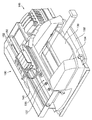
図1は、本発明のプリントヘッド構造を組み込むことのできるインクジェットプリントカートリッジ10の1つの斜視図である。図1のプリントカートリッジ10は、その本体12内にかなりの量のインクを含むタイプであるが、他の好適なプリントカートリッジとしては、プリントヘッドに搭載されているかまたは管によってプリントヘッドに接続されている外部インク供給源からインクを受け取るタイプであってもよい。
【0014】
インクはプリントヘッド14に供給される。以下で詳述するプリントヘッド14は、インク射出要素を含むそれぞれのインク射出チャンバ内へインクを流し込む。接点16に電気信号が供給されてインク射出要素を個別に通電し、関連するノズル18を通してインク滴が射出される。従来のプリントカートリッジの構造および動作は、非常によく知られている。
【0015】
図2は、図1のプリントヘッドを2−2線に沿って切った部分断面図である。1つのプリントヘッドは、300個以上のノズル及びそれに関連するインク射出チャンバを有することができるが、本発明を理解するためには、1つのインク射出チャンバのみの詳細を説明すればよい。当業者にはまた、複数のプリントヘッドが単一のシリコンウェーハ上に形成され、従来技術を用いて互いから分離されるということも理解されるはずである。
【0016】
図2において、シリコン基板20の上に様々な薄膜層22が形成されている。これについては、以下で詳細に説明する。薄膜層22には、抵抗器24を形成するための抵抗層が含まれる。その他の薄膜層は、基板20からの絶エッジ、ヒータ抵抗器要素から基板20への熱伝導経路の提供、抵抗器要素への導体の提供など様々な機能を果たす。一つの導体が、抵抗器24の一端に通じていることが示されている。同様の導体が、抵抗器24の他端にも通じている。実際の実施形態においては、チャンバ内の抵抗器および導体は上の層に覆い隠される。
【0017】
薄膜層22を完全に貫通してインク供給穴26が形成される。1個のチャンバに複数の穴を形成することができる。代わりに、インク射出チャンバ30の並びに対して共通のインクチャネルを設けるためオリフィス層28にマニホルドを形成してもよい。
【0018】
薄膜層22の表面上にオリフィス層28が堆積されエッチングされて、1個の抵抗器24当たり1個のインク射出チャンバ30を形成する。ノズル34は、従来の写真平板技術を用いて形成してもよい。
【0019】
シリコン基板20をエッチングして、インク供給穴26の行の並びの長さ方向に沿って延びるトレンチ36を形成し、インクリザーバからのインク38がインク供給穴26に入り、インク射出チャンバ30へインクを供給することができるようになっている。後述する2段階のエッチング工程は、トレンチ36のエッジをインク供給穴26と精確に整合させるために用いられる。
【0020】
一実施形態において、それぞれのプリントヘッドは長さが約1/2インチであり、2つのオフセットされたノズルの行を含む。それぞれの行は150個のノズルを含み、1個のプリントヘッド当たり全部で300個のノズルがある。したがってプリントヘッドは、ノズルの行の方向について、シングルパスで1インチ当たり600ドット(600dpi)の解像度で印刷することができ、マルチパスではそれよりも高い解像度で印刷することができる。また、プリントヘッドの走査方向についても、それよりも高い解像度で印刷することができる。本発明を用いて1200dpi以上の解像度を得ることができる。
【0021】
動作について述べると、ヒータ抵抗器24に電気信号が供給され、これによってインクの一部が気化され、インク射出チャンバ30内に気泡が形成される。この気泡は、関連するノズル34を通して媒体上へインク滴を進ませる。そして、インク射出チャンバ30は、毛管作用によって再補充される。
【0022】
図3は、図2のプリントヘッドを下から見た図であり、プリントヘッドに形成された2つの平行なインク射出チャンバのアレイが示されている。2行のインク射出チャンバ30は、オフセットされてもよい。様々な図において同じ数字で示す要素は、同様または同一のものであってもよい。
【0023】
トレンチよりも上にある棚状の薄膜層は、膜と呼ばれる。この膜の幅を、図3において破線40で示す。図2のプリントヘッドを形成する特定の方法は、2段階のトレンチエッチング工程を用いる。第1のトレンチエッチングの結果、破線42で示す膜幅になるが、これは最終的な膜幅40よりも狭い。後述するように、これによって、第1のトレンチエッチング用のマスクを、きわめてゆとりのある公差にすることができる。第2のトレンチエッチングの後、トレンチの側壁は、薄膜層により規定されるインク供給穴26に自己整合される。
【0024】
図4は、図2の4−4のラインに沿って切った断面図であり、第2の行のインク射出チャンバを含めたプリントヘッドの補足的な部分を示している。抵抗器24を含む薄膜層22が簡略化されて示されている。図4のさらなる詳細については、図5および図6A〜Gに関連して説明する。
【0025】
図5は、図2の4−4のラインに沿って切った断面図であり、単一のインク射出チャンバと、これに関連するプリントヘッドの構造を示している。図5は個々の薄膜層の一実施形態を示しており、図6A〜Gは、図2〜5のプリントヘッドを製造するのに用いる様々な工程を示す。特に言及しない限り、これらの工程には、従来の堆積、マスキング、およびエッチング等の工程が用いられる。
【0026】
図6Aにおいて、結晶方位が<100>のシリコン基板20が、真空チャンバ内に配置される。バルクシリコンは、厚さが約675μmである。
【0027】
従来の技術を用いて、シリコン基板20の上に厚さが1.2μmのフィールド酸化物層46が形成される。次に、従来の技術を用いて、フィールド酸化物層46の上に厚さ0.5μmのPSG(燐酸シリケートガラス)層48が堆積される。
【0028】
従来の写真平板技術を用いて、PSG層48の上にマスク49が形成される。マスク49は、図3および図7にも示されている。次に、従来の反応性イオンエッチング(RIE)を用いて、PSG層48をエッチングし、PSG層48を、次に形成するインク供給穴から引っ込めておく。これによって、PSG層48がインクから保護される。
【0029】
PSG層48の代わりにBPSGまたはTEOS(BTEOS)層を用い、層48と同様の方法でエッチングを施してもよい。
【0030】
図6Bにおいて、マスク49が除去され、次にPSG層48上に、例えば厚さ0.1μmのタンタルアルミニウム(TaAl)などの抵抗層50が堆積される。また、他の既知の抵抗層を用いることもできる。次に、AlCuの導電層25が、TaAlの上に堆積される。マスク54が堆積されて従来の写真平板技術を用いてパターニングされ、従来のIC製造技術を用いて導電層25および抵抗層50がエッチングされる。別のマスキングおよびエッチング工程(図示せず)を用いて、図2に示すように、AlCuのうちのヒータ抵抗器24の上にある部分が除去される。結果として得られるAlCuの導体は、図6A〜Gの視界外にある。
【0031】
導電層25と抵抗層50をエッチングすることによって、第1の抵抗器寸法(例えば、幅)が規定される。第2の抵抗器寸法(例えば、長さ)は、導電層25をエッチングし、抵抗部が導電トレースに2つの端部で接触するようにすることによって規定される。抵抗器および導体を形成するこの技術は、当該分野において周知である。導電トレースは、プリントヘッドの中央を横切っては延びず、エッジに沿って延びるように形成される。基板20上には、通電信号を抵抗器24に供給する適切なアドレス指定回路およびパッドが設けられる。
【0032】
図6Cにおいて、抵抗器24および導電層25の上に、厚さ0.5μmの窒化ケイ素層56を形成する。この層は、絶縁およびパッシベーションを行う。
【0033】
窒化ケイ素層56上に、厚さ0.25μmの炭化ケイ素層58を形成して、さらなる絶縁およびパッシベーションを行う。窒化ケイ素層56および炭化ケイ素層58によって、PSG層48がインクおよび腐食液から保護されることになる。窒化ケイ素や炭化ケイ素の代わりに、他の絶縁体層を用いてもよい。
【0034】
次に、これらのパッシベーション層はマスクされ(視界外)、従来の技術を用いてエッチングされて導電層25の一部が露出され、後に接地線を設けるための金の導電層に電気的に接触される。
【0035】
次に、炭化ケイ素層58上に、タンタル(Ta)の気泡キャビテーション層60が形成される。タンタル層60上には、金(Au)62が堆積されてエッチングされ、導電層25のトレースのうち特定の一つに電気的に接続された接地線を形成する。接地線は、基板20のエッジに沿ったボンディングパッドにより終端される。
【0036】
AlCuおよび金の導体は、基板表面上に形成されたトランジスタに結合してもよい。このようなトランジスタは、前述の米国特許第5,648,806号において説明されている。
【0037】
図6Dにおいて、マスク66がパターニングされ、露出された薄膜層の一部がエッチングにより取り除かれ、インク供給穴26(図2)が形成される。または、様々な薄膜層を形成するときにマスキング及びエッチングインクを行い、複数のマスキング及びエッチング工程を用いて供給穴をエッチングすることもできる。
【0038】
次に、異方性エッチングを用いて、各薄膜層がエッチングされる。このインク供給穴エッチング工程は、いくつかのタイプのエッチング(RIEまたはウェットエッチング)を組み合わせたものであってもよい。各薄膜層をエッチングして貫通する方法は、従来のIC製造技術を用いてもよい。エッチングが行われた後のウェーハが、図6Eに示されている。
【0039】
図2のトレンチ36を形成するとき、裏側のトレンチマスクを完全にインク供給穴26に整合させることは困難である。後述する製造工程は、トレンチ36をインク供給穴26に整合させる技術を含む。
【0040】
図6Fにおいて、従来の写真平板技術を用いて、表側の保護層70が堆積され形成される。一実施形態において、保護層70は、バッファード酸化物エッチング(BOE)で素早く容易に除去することができるほど充分薄いが、約15時間のトレンチエッチングの間TMAH(水酸化テトラメチルアンモニウム)の腐食液への露出に耐えることができるほど充分厚い厚さ(例えば、1000オングストローム=10-7m)のプラズマTEOSである。保護層70は、酸化物、窒化物、および酸窒化物を含む、任意の適切な材料であってもよい。この操作を行うためのマスクは、インク供給穴のマスクを反転させたものであるが、それよりもわずかに大きくなっていて、インク供給穴の開口部全体が保護層70に覆われることを保証している。保護層70のマスクの境界を図3に示す。
【0041】
図6Gを参照して、次にオリフィス層28が堆積して形成される。オリフィス層28は、SU8と呼ばれるスピンコートしたエポキシで形成されてもよい。またはオリフィス層28は、張り合わせやスクリーン印刷で形成してもよい。一実施形態において、このオリフィス層は約20μmである。インク射出チャンバ30(図2)およびノズル34は、写真平板によって形成される。一つの方法としては、半照射量の紫外線放射を用いる第1のマスクによって、ノズル34が形成される位置を除いてSU8の上面が「硬化」させられる。次に、全照射量の紫外線を用いる第2のマスクによって、ノズル34またはインク射出チャンバ30のいずれも形成されない領域において、SU8が露光される。これら2回の露光の後、SU8は現像され、硬化した部分は残るが、SU8のノズル部分及びインク射出チャンバ部分は除去される。
【0042】
薄膜層および形成したオリフィス層28が図4に示されている。
【0043】
次に、従来の技術を用いてウェーハの裏側をマスキングし(マスク76によって)、ウェーハの裏側のうちの、TMAHのトレンチエッチングを行う部分を露出する。裏側のマスク76は、従来の写真平板技術を用いて形成したFOXのハードマスクであってもよい。ウェーハを、ウェットなTMAH腐食液に浸漬する。それによって、図4に示すような斜めの断面が形成される(破線78で示される)。この第1のエッチングは、FOX層46および保護層70を貫通してエッチングするのに充分な時間だけ行われる。この第1のエッチングの後の、トレンチの壁のうちの破線78の部分は、上へ延びてインク供給穴領域内に入る。その結果得られるトレンチの壁間の膜幅は、図3に破線42で示される。トレンチ幅は、典型的には200μmよりも狭く、一実施形態において、20〜60μmの間である。裏側のマスキングは、整合ずれに対して大きなマージンがある。このような整合ずれがあると、通常は、インク供給穴の領域が制限され、プリントヘッドの流体特性に悪影響を及ぼしてしまう。しかし、後述の工程によって、このような整合ずれの悪影響が回避される。
【0044】
次に、このウェーハはBOE溶液内に置かれ、BOE溶液によって保護層70が除去される。取り除かれた保護層70の像が、図4に示されている。
【0045】
次にウェーハには、再びTMAHウェットエッチングが行われる。このエッチングにおいては、腐食液は、シリコンのうちインク供給穴26を通して露出した部分に接触する。これによって、本来的に、図4に示すようなインク供給穴26のエッジに自己整合した斜めのエッチングが行われる。この第2のトレンチエッチングの間、トレンチはインク供給穴のエッジに達するまで急速に幅が広がる。図3および図4は、意図的にインク供給穴26に関して整合がずれた(図3の線42を参照されたい)第1のトレンチエッチングを示しており、第2のエッチングの後に得られるトレンチが、インク供給穴に整合したエッジを有することを示している(図3の線40を参照されたい)。
【0046】
一実施形態において、トレンチ36は、インク射出チャンバの行方向の長さまで延びている。ウェットまたはドライであれ、種々のエッチング技術のうちのいずれを用いてもよい。ドライエッチングには、例えばXeF2やSiF6が含まれる。適切なウェットエッチングには、例えばエチレンジアミンピロカテコール(EDP)、水酸化カリウム(KOH)、およびTMAHが含まれる。他のエッチングもまた、用いることができる。これらのうちいずれか一つまたはこれらの組み合わせも、この用途に用いることができる。
【0047】
結果として得られたウェーハは次に切断されて、個々のプリントヘッドが形成される。プリントヘッド上の導体への電気的アクセスには、フレキシブル回路が用いられる。結果として得られる装置は、次に、図1に示されるように、プラスチックのプリントカートリッジに取り付けられ、プリントヘッドはプリントカートリッジ本体に関してシールされ、インク漏れが防止される。
【0048】
薄膜層の形成のさらなる詳細については、本願の出願人に譲渡されその参照によって本明細書に組み込まれる、Naoto Kawamura他による1999年8月27日出願の「Fully Integrated Thermal Inkjet Printhead Having Thin Film Layer Shelf」と題された米国特許出願第09/384,817号において見ることができる。
【0049】
一実施形態において、オリフィス層28はまた、比較的大きなインク粒子がチャンバ30内に入ることを防止するための柱80、82(図4)も提供するように形成される。図3は、それぞれのチャンバについてこのような柱を4つ、輪郭を破線で示している。柱80、82は、チャンバ30を形成するのに用いるのと同じ技術で形成してもよい。
【0050】
トレンチ36は、プリントヘッドの長さまで延ばすこともできるし、または、プリントヘッドの機械的強度を改善するために、プリントヘッドのインク射出チャンバの下にある部分の長さまで延ばしてもよい。基板とインクの反応が心配な場合は、パッシベーション層を基板20上に堆積してもよい。
【0051】
図7および図8は、本発明の他の実施形態を示す。この実施形態は、インク供給穴部分の薄膜層のエッチングがプリントヘッドの中央部を横切るように拡張して行われること、及び、インク供給穴の境界を規定するためにオリフィス層85が用いられることを除外すれば、図4〜図6Gに示す各工程とほぼ同一の工程により形成される。
【0052】
図7からわかるように、インク供給穴のマスク86は、2つの互いに対向するインク射出チャンバ30の間に延びており、表側の保護マスク88のほうがわずかに大きい。幅の狭い薄膜の壁が、プリントヘッドの中央部におけるエッチングされた領域同士を分離している。
【0053】
図9および図10は、図7および図8の構造の変形を示しており、エッチングにより形成されるインク供給穴のマスク92は、薄膜層22に大きな中央の長方形開口部98を形成するのに用いられる。表側の保護マスク94は、保護層96(図10)を形成するのに用いられる。オリフィス層85は、インク供給穴の境界の一部を形成する。
【0054】
図11および図12は、上述の各工程の変形を示しており、この例では、個別の保護層は形成しない。この工程において、FOX層46(図6Aにも示す)がインク供給穴領域の保護層として機能する。図7および図8とは対照的に、薄膜層は、従来の技術を用いて、FOX層46までしかエッチングされない。第1のトレンチエッチングを行った後、トレンチの壁78は、インク供給穴に大まかに整合させられるのみである。次に、BOEまたはその他の適切なエッチングを用いて、露出しているFOX層46を除去する(除去されたFOX層の輪郭は、図12に点線で示される)。前述と同様に、第2のトレンチエッチングが実施され、その結果、トレンチの壁が薄膜開口部に整合されられる。インク供給穴のマスク86は、図7と同様のものが示されているが、図3および図9のインク供給穴のマスクを用いることもできる。図11および図12の工程では、個別の保護層を形成する必要がないため、ウェーハ処理においてかなりの費用が節約される。
【0055】
トレンチの壁の上に突き出ている棚状の短い膜を、様々な図において示し、第2のエッチングの時間が決定的に重要なものではないということを示している。トレンチの壁がエッチングされ、薄膜開口部を通過すると、基板のエッチングは大幅に減速される。
【0056】
集積回路製造の当業者であれば、本明細書で説明されるプリントヘッド構造を形成するのに、様々な技術が用られることが分かるであろう。本発明の利点が得られるならば、薄膜層やそれらの厚さは様々なものでかまわないし、なくてもよい層もある。さらなるインク供給穴のパターンもまた考えられる。
【0057】
図13は、本発明を組み込むことができるインクジェットプリンタ130の一実施形態を示している。インクジェットプリンタの数多ある他の設計もまた、本発明と共に用いることができる。インクジェットプリンタのさらなる詳細については、その参照によって本明細書に援用されるNorman Pawlowski他による米国特許番号第5,852,459号において見られる。
【0058】
インクジェットプリンタ130は、紙134を収容する入力トレイ132を有する。紙134は、印刷されている間、ローラ137を用いてプリント領域135を通して送られる。次に、紙134は出力トレイ136に送られる。可動キャリッジ138はプリントカートリッジ140〜143を保持しており、これらはそれぞれ、シアン(C)、ブラック(K)、マゼンタ(M)、およびイエロー(Y)のインクを印刷する。
【0059】
一実施形態において、交換式インクカートリッジ146内のインクが、柔軟性を有するインク管148を経由してそれぞれ関連するプリントカートリッジに供給される。また、プリントカートリッジは、かなりの量の流体を保持するタイプであってもよく、再補充可能であっても再補充可能でなくてもよい。他の実施形態では、インク供給源はプリントヘッド部とは分離されており、キャリッジ138のプリントヘッドに取り外しできるように取りつけられる。
【0060】
キャリッジ138は、従来のベルトと滑車のシステムにより走査方向に沿って移動され、摺動ロッド150に沿って摺動する。他の実施形態では、キャリッジは静止式であり、静止したプリントカートリッジのアレイが、移動する紙の上に印刷を行う。
【0061】
従来の外部コンピュータ(例えば、PC)からの印刷信号が、プリンタ130によって処理されて、印刷するドットのビットマップが生成される。このビットマップは、次に、プリントヘッドに対する発射信号へ変換される。印刷中に走査方向に沿って往復して横切るときのキャリッジ138の位置は、キャリッジ138上の光電素子により光学的エンコーダのストリップ152が検出されてこれによって判定される。この位置の判定により、それぞれのプリントカートリッジ上の様々なインク射出要素は、キャリッジの走査中、適切な時点で選択的に発射される。
【0062】
プリントヘッドは、抵抗式、圧電式、またはその他のタイプのインク射出要素を用いてもよい。
【0063】
キャリッジ138のプリントカートリッジが紙を横切って走査するとき、プリントカートリッジにより印刷されるスワスは重なり合う。1回以上の走査の後、紙134は出力トレイ136の方向へシフトされ、キャリッジ138は走査を再開する。
【0064】
本発明は、グリットホイール、ロールフィード、ドラムまたは真空ベルト等の技術を組み込んで印刷媒体をプリントヘッドアセンブリに対して支持及び移動させる印刷システムのような、代替的な媒体またはプリントヘッド移動機構を利用した代替的な印刷システム(図示せず)にも、同じように適用することができる。グリットホイールの設計では、グリットホイールとピンチローラが、媒体を一定方向に往復させる一方で、1つ以上のプリントヘッドアセンブリを有するキャリッジが、その方向と直交する方向に沿って媒体を走査する。ドラムプリンタの設計では、媒体は、一定方向に回転する回転ドラムに取りつけられ、1つ以上のプリントヘッドアセンブリを有するキャリッジが、その方向と直交する方向に沿って媒体を走査する。ドラムの設計またはグリットホイールの設計のいずれの場合においても、走査は、一般に、図13に示すシステムのように往復させる方法で行われることはない。
【0065】
単一の基板上に、多数のプリントヘッドを形成してもよい。さらに、プリントヘッドのアレイを、1ページの幅全体にわたって配列し、プリントヘッドによる走査が不要であるようにしてもよい。その場合、紙はアレイに対して垂直にシフトするのみである。
【0066】
他のカラーまたは定着材を含む追加的なカートリッジが、キャリッジに設けられてもよい。
【0067】
ここまで本発明の特定の実施形態を示し説明してきたが、当業者には、本発明の広い態様において本発明から逸脱することなく変更および変形を行うことが可能であることは明らかであり、したがって、付加する特許請求の範囲は、すべてのそのような変更および変形が、本発明の真の思想および権利範囲内にあるものとしてその範囲内に包含されることを意図している。
【0068】
以下においては、本発明の種々の構成要件の組み合わせからなる例示的な実施態様を示す。
1.プリント装置を形成する方法であって、
プリントヘッド基板(20)を設けるステップと、
前記基板の第1の表面に複数の薄膜層(22)を形成し、前記薄膜層のうちの少なくとも1つが複数のインク射出要素(24)を形成するようにするステップと、
前記薄膜層のうちの少なくともいくつかを貫通してインク供給開口部(26)を形成するステップと、
前記インク供給開口部と前記基板との間に、保護層(46,70,96)を設けるステップと、
トレンチエッチングを行うため前記基板の第2の表面をマスキング(76)するステップと、
前記基板の前記第2の表面をエッチングして、第1のトレンチ部(78)を形成するステップと、
前記保護層を、少なくとも前記インク供給開口部と前記基板との間で除去するステップと、
前記基板の前記インク供給開口部を通して露出した部分をさらにエッチングして、前記トレンチ(36)のエッジを実質的に前記インク供給開口部に自己整合させるステップと、
からなる方法。
2.前記薄膜層(22)はフィールド酸化物層(46)を含み、前記保護層は、前記薄膜層がエッチングされて前記インク供給開口部(26)を形成した後に残される前記フィールド酸化物層の一部である、項番1の方法。
3.前記保護層を設けるステップは、前記インク供給開口部(26)を形成した後に前記インク供給開口部内に保護層(70,96)を形成するステップを含む、項番1の方法。
4.前記インク供給開口部(26)を形成するステップは、前記薄膜層(22)を完全に貫通して開口部を形成するステップを含む、項番1の方法。
5.前記方法は、前記薄膜層(22)の上にオリフィス層(28,85)を形成するステップをさらに含み、前記オリフィス層は複数のインク射出チャンバ(30)を規定し、それぞれのチャンバは内部にインク射出要素(24)を有し、前記オリフィス層はさらに、それぞれのインク射出チャンバのノズル(34)を規定する、項番1の方法。
6.前記保護層(46,70,96)を除去する前記ステップは、ウェット腐食液を前記チャンバ(30)に入れて前記保護層をエッチングさせるようにウェットエッチングを行うステップを含む、項番5の方法。
7.前記オリフィス層(28)の中央部は、薄膜の上に重なっている、項番5の方法。
8.前記オリフィス層(85)は、前記インク供給開口部によって部分的に形成されるインク供給穴(26)の境界を確定する項番5の方法。
9.前記保護層(70)を設けるステップは、TEOSを堆積するステップを含む、項番1の方法。
10.前記保護層(46,70,96)を設けるステップは、酸化物、窒化物、および酸窒化物からなるグループから選択された材料を堆積するステップを含む、項番1の方法。
11.前記保護層を設けるステップは、インク供給開口部の領域よりも広い領域にわたって保護層(46,70,96)を形成するステップを含む、項番1の方法。
12.前記インク供給開口部(26)を形成するステップは、それぞれのインク射出要素(24)の付近のみにインク供給開口部を形成するステップを含む、項番1の方法。
13.前記インク供給開口部(26)を形成するステップは、前記基板(20)の中央部を横切って延びる細長いインク供給開口部(86)を形成するステップを含む、項番1の方法。
14.前記インク供給開口部(26)を形成するステップは、前記基板(20)の中央部に長方形のインク供給開口部(92)を形成するステップを含む、項番1の方法。
15.前記基板に直接隣接する前記薄膜層の下層(46)および前記保護層(46,70,96)は、前記基板の前記第2の表面をエッチングして前記第1のトレンチ部(78)を形成するステップに関して、エッチング停止として機能する、項番1の方法。
16.前記基板(20)の前記第2の表面をエッチングして第1のトレンチ部(78)を形成するステップは、前記基板をTMAH溶液でエッチングして、前記第2の表面に関して斜めのトレンチエッジを形成するステップを含む、項番1の方法。
17.製造途中のプリントヘッドであって、
プリントヘッド基板(20)と、
前記基板の第1の表面上に形成された複数の薄膜層(22)であって、前記薄膜層のうちの少なくとも1つが複数のインク射出要素(24)を形成するように構成される複数の薄膜層と、
前記薄膜層のうちの少なくともいくつかを貫通して形成されたインク供給開口部(26)と、
前記インク供給開口部と前記基板の間に設けられた保護層(46,70,96)と、
前記基板を貫通し、前記インク供給開口部と前記基板の間の前記保護層までエッチングして形成されるトレンチ(78)であって、第2のトレンチエッチングの後、前記インク供給開口部と前記基板の間の前記保護層が取り除かれ、前記インク供給開口部に実質的に整合された壁を有するトレンチを形成するトレンチと、
からなるプリントヘッド。
18.前記薄膜層(22)はフィールド酸化物層(46)を含み、前記保護層は、前記薄膜層(22)がエッチングされた後に残る前記フィールド酸化物層の一部である、項番17のプリントヘッド。
19.前記保護層(70,96)は、前記インク供給開口部(26)を形成した後に前記インク供給開口部内に形成される、項番17のプリントヘッド。
20.前記インク供給開口部(26)は、前記薄膜層(22)を完全に貫通して形成される、項番17のプリントヘッド。
21.前記プリントヘッドは、さらに前記薄膜層の上に形成されたオリフィス層(28,85)を含み、前記オリフィス層が複数のインク射出チャンバを規定し、前記チャンバのそれぞれが前記チャンバの内部にインク射出要素を有し、前記オリフィス層がさらに、インク射出チャンバのそれぞれに対してノズルを規定する、項番17のプリントヘッド。
22.スルーホールを形成するための方法であって、
基板(20)を設けるステップと、
前記基板の第1の表面に複数の薄膜層(22)を形成するステップと、
前記薄膜層のうちの少なくともいくつかを貫通して、開口部(26)を形成するステップと、
前記開口部と前記基板の間に、保護層(46,70,96)を設けるステップと、
前記基板の第2の表面をマスキング(76)してトレンチエッチングを行うステップと、
前記基板の前記第2の表面をエッチングして、第1のトレンチ部(78)を形成するステップと、
前記保護層を、前記開口部と前記基板の間で除去するステップと、
前記基板の前記開口部を通して露出した部分をさらにエッチングして、前記トレンチ(36)のエッジを実質的に前記開口部に自己整合させるステップと、
からなる方法。
23.前記薄膜層(22)はフィールド酸化物層(46)を含み、前記保護層は、前記薄膜層がエッチングされて前記開口部(26)を形成した後に残る前記保護層の一部である、項番22の方法。
24.前記保護層を設けるステップは、前記開口部が形成された後に前記開口部内に保護層(70,96)を形成するステップを含む、項番22の方法。
25.前記開口部(26)を形成するステップは、前記薄膜層(22)を完全に貫通して開口部を形成するステップを含む、項番22の方法。
26.前記保護層(70,96)を設けるステップは、TEOSを堆積するステップを含む、項番22の方法。
27.前記保護層(46,70,96)を設けるステップは、酸化物、窒化物、および酸窒化物からなるグループから選択される材料を堆積するステップを含む、項番22の方法。
28.前記保護層を設けるステップは、開口部の領域よりも広い領域にわたって保護層(46,70,96)を形成するステップを含む、項番22の方法。
29.前記基板(20)の前記第2の表面をエッチングして第1のトレンチ部(78)を形成するステップは、前記基板をTMAH溶液でエッチングして、前記第2の表面に関して斜めのトレンチエッジを形成するステップを含む、項番22の方法。
【0069】
【発明の効果】
本発明は、上記のように構成することにより、非常に精密な公差で製造可能なモノシリック構造のプリントヘッドが提供できる。
【図面の簡単な説明】
【図1】本明細書において説明するプリントヘッドのいずれか1つを組み込むことのできるプリントカートリッジの一実施形態の斜視図である。
【図2】本発明によるプリントヘッドの一実施形態の一部の切欠き斜視図である。
【図3】図2に示すプリントヘッドを上から見下ろした部分的な透視図であり、プリントヘッドのさらなる一部を示している。
【図4】図2の4−4線に沿った断面図であり、プリントヘッドのさらなる一部を示している。
【図5】図2のプリントヘッド部を4−4線に沿って切った断面図であり、薄膜層のさらなる詳細を示している。
【図6A】一製造工程における図4のプリントヘッドの一部の4−4線に沿った断面図である。
【図6B】一製造工程における図4のプリントヘッドの一部の4−4線に沿った断面図である。
【図6C】一製造工程における図4のプリントヘッドの一部の4−4線に沿った断面図である。
【図6D】一製造工程における図4のプリントヘッドの一部の4−4線に沿った断面図である。
【図6E】一製造工程における図4のプリントヘッドの一部の4−4線に沿った断面図である。
【図6F】一製造工程における図4のプリントヘッドの一部の4−4線に沿った断面図である。
【図6G】一製造工程における図4のプリントヘッドの一部の4−4線に沿った断面図である。
【図7】プリントヘッドの第2の実施形態を上から見下ろした部分的な透視図である。
【図8】第2の実施形態のプリントヘッドの断面図である。
【図9】図7及び図8の構造の変形を示す図であり、薄膜層を貫通して中央の長方形のインク供給領域が形成されていることを示している。
【図10】図7及び図8の構造の変形を示す図であり、薄膜層を貫通して中央の長方形のインク供給領域が形成されていることを示している。
【図11】図7及び図8の構造の変形を示す図であり、別個の保護層を形成する代わりにFOX層を保護層として用いる例を示している。
【図12】図7及び図8の構造の変形を示す図であり、別個の保護層を形成する代わりにFOX層を保護層として用いる例を示している。
【図13】媒体への印刷のため本発明のプリントヘッドを内部に取り付けることのできる従来のインクジェットプリンタを示す斜視図である。
【符号の説明】
20 シリコン基板
22 薄膜層
24 抵抗器
26 インク供給穴
28、85 オリフィス層
30 インク射出チャンバ
34 ノズル
36 トレンチ
46 FOX層
70、96 保護層
76 マスク
78 破線
86 インク供給穴
92 インク供給穴のマスク[0001]
BACKGROUND OF THE INVENTION
The present invention relates to ink jet printers, and more particularly to monolithic print heads for ink jet printers.
[0002]
[Prior art]
Inkjet printers typically have a printhead attached to a carriage that reciprocally scans across the width of the paper supplied to the printer. Whether the ink reservoir is mounted on the carriage or external to the carriage, ink from the ink reservoir is supplied to the ink ejection chamber on the printhead. Each ink ejection chamber includes ink ejection elements, such as heater resistors and piezoelectric elements, which can be operated independently. By energizing the ink ejection element, an ink drop is ejected through the nozzle, producing a small dot on the medium. The generated dot pattern forms an image or text.
[0003]
US Pat. No. 5,648,806 entitled “Stable Substrate Structure For A Wide Swath Nozzle Array In A High Resolution Inkjet Printer” by Steven Steinfield et al., Assigned to the assignee of the present application and incorporated herein by reference. The issue provides further information on one particular type of printhead and inkjet printer.
[0004]
[Problems to be solved by the invention]
As printhead resolution and printing speeds increase to meet the demanding demands of the consumer market, new printhead manufacturing techniques and structures are needed.
[0005]
[Means for Solving the Problems]
This specification describes a monolithic printhead formed using integrated circuit technology. A thin film layer including a resistance layer is formed on the upper surface of the silicon substrate. These various layers are etched to form a conductor to the heater resistor element. A piezoelectric element may be used instead of the resistor element.
[0006]
For each ink ejection chamber, at least one ink supply hole (ink supply opening) is formed through the thin film layer. In one embodiment, a protective layer is deposited over the ink supply hole area.
[0007]
An orifice layer is formed on the top surface of the thin film layer to define nozzles and ink ejection chambers. In one embodiment, a light definable material is used to form the orifice layer.
[0008]
A trench mask is formed on the bottom surface of the substrate. The trench is etched through the exposed bottom surface of the substrate (eg, using TMAH). The trench completely removes the portion of the substrate below the ink supply hole by etching. The protective layer prevents TMAH from etching the substrate from the front side through the ink supply hole.
[0009]
Next, the protective layer is removed, and second trench etching is performed. The TMAH solution removes the exposed portion of the substrate through the ink supply hole by etching. The second trench etch inherently aligns the edges of the trench with the ink supply holes. This two-stage trench etching relaxes the tolerances for the trench mask and allows the trench to be precisely positioned. This is because the trench sidewalls eventually align with the thin film openings.
[0010]
In other embodiments, a separate protective layer is not deposited. Instead, a field oxide (FOX) layer formed on the substrate as one of the thin film layers is used for protection. An ink supply hole is etched through the thin film layer to the FOX layer. Similar to the previous embodiment, a first trench etch is performed. The portion of the FOX layer that is in the ink supply hole region is removed by buffered oxide etching. A second trench etch is then performed, which causes the trench sidewalls to self-align with the thin film openings. This process is more economical than the previous embodiment using a separate protective layer.
[0011]
The resulting fully integrated thermal inkjet printhead can be manufactured with very close tolerances due to the monolithic overall structure and meets the requirements for next generation printheads.
[0012]
This process can also be used to form openings in devices other than print heads.
[0013]
DETAILED DESCRIPTION OF THE INVENTION
FIG. 1 is a perspective view of one
[0014]
Ink is supplied to the
[0015]
FIG. 2 is a partial cross-sectional view of the print head of FIG. 1 taken along line 2-2. A single printhead can have more than 300 nozzles and associated ink ejection chambers, but in order to understand the present invention, only one ink ejection chamber need be described in detail. It should also be understood by those skilled in the art that multiple printheads are formed on a single silicon wafer and separated from each other using conventional techniques.
[0016]
In FIG. 2, various thin film layers 22 are formed on a
[0017]
An
[0018]
An
[0019]
The
[0020]
In one embodiment, each printhead is approximately 1/2 inch in length and includes two offset nozzle rows. Each row contains 150 nozzles, for a total of 300 nozzles per printhead. Therefore, the print head can print at a resolution of 600 dots per inch (600 dpi) in a single pass in the row direction of the nozzles, and can print at a higher resolution in multi-pass. In addition, printing can be performed with a higher resolution in the scanning direction of the print head. A resolution of 1200 dpi or higher can be obtained using the present invention.
[0021]
In operation, an electrical signal is supplied to the
[0022]
FIG. 3 is a bottom view of the printhead of FIG. 2, showing an array of two parallel ink ejection chambers formed in the printhead. The two rows of
[0023]
The shelf-like thin film layer above the trench is called a film. The width of this film is indicated by a
[0024]
FIG. 4 is a cross-sectional view taken along line 4-4 of FIG. 2, showing the supplemental portion of the printhead including the second row of ink ejection chambers. A
[0025]
FIG. 5 is a cross-sectional view taken along line 4-4 of FIG. 2, showing a single ink ejection chamber and the associated printhead structure. FIG. 5 illustrates one embodiment of individual thin film layers, and FIGS. 6A-G illustrate various processes used to manufacture the printhead of FIGS. Unless otherwise noted, conventional processes such as deposition, masking, and etching are used for these processes.
[0026]
In FIG. 6A, a
[0027]
A
[0028]
A
[0029]
Instead of the
[0030]
In FIG. 6B, the
[0031]
By etching the
[0032]
In FIG. 6C, a
[0033]
A
[0034]
These passivation layers are then masked (out of sight) and etched using conventional techniques to expose a portion of the
[0035]
Next, a
[0036]
The AlCu and gold conductors may be coupled to a transistor formed on the substrate surface. Such a transistor is described in the aforementioned US Pat. No. 5,648,806.
[0037]
In FIG. 6D, the
[0038]
Next, each thin film layer is etched using anisotropic etching. This ink supply hole etching process may be a combination of several types of etching (RIE or wet etching). As a method of etching and penetrating each thin film layer, a conventional IC manufacturing technique may be used. The wafer after it has been etched is shown in FIG. 6E.
[0039]
When forming the
[0040]
In FIG. 6F, a front
[0041]
Referring to FIG. 6G, an
[0042]
The thin film layer and the formed
[0043]
Next, the back side of the wafer is masked (by mask 76) using conventional techniques to expose the portion of the back side of the wafer where TMAH trench etching is performed. The
[0044]
Next, the wafer is placed in a BOE solution, and the
[0045]
Next, TMAH wet etching is again performed on the wafer. In this etching, the corrosive liquid contacts the exposed portion of the silicon through the
[0046]
In one embodiment, the
[0047]
The resulting wafer is then cut to form individual printheads. A flexible circuit is used for electrical access to the conductors on the printhead. The resulting device is then attached to a plastic print cartridge, as shown in FIG. 1, and the print head is sealed with respect to the print cartridge body to prevent ink leakage.
[0048]
For further details of forming thin film layers, see “Fully Integrated Thermal Inkjet Printhead Having Thin Film Layer Shelf” filed Aug. 27, 1999 by Naoto Kawamura et al., Assigned to the assignee of the present application and incorporated herein by reference. In US patent application Ser. No. 09 / 384,817.
[0049]
In one embodiment, the
[0050]
The
[0051]
7 and 8 show another embodiment of the present invention. In this embodiment, the etching of the thin film layer in the ink supply hole portion is performed so as to extend across the center of the print head, and the
[0052]
As can be seen from FIG. 7, the ink
[0053]
FIGS. 9 and 10 show a variation of the structure of FIGS. 7 and 8, where the ink
[0054]
FIG. 11 and FIG. 12 show a modification of each of the above-described steps. In this example, no individual protective layer is formed. In this step, the FOX layer 46 (also shown in FIG. 6A) functions as a protective layer for the ink supply hole region. In contrast to FIGS. 7 and 8, the thin film layer is only etched down to the
[0055]
A shelf-like short film protruding above the trench wall is shown in the various figures, indicating that the time of the second etch is not critical. As the trench walls are etched and pass through the thin film openings, the etching of the substrate is greatly slowed.
[0056]
Those skilled in the art of integrated circuit manufacturing will appreciate that various techniques can be used to form the printhead structures described herein. If the advantages of the present invention are obtained, the thin film layers and their thicknesses may vary and some layers may be omitted. Additional ink supply hole patterns are also contemplated.
[0057]
FIG. 13 illustrates one embodiment of an
[0058]
The
[0059]
In one embodiment, the ink in the
[0060]
The
[0061]
A print signal from a conventional external computer (eg, PC) is processed by the
[0062]
The printhead may use resistive, piezoelectric, or other types of ink ejection elements.
[0063]
As the print cartridge on
[0064]
The present invention utilizes alternative media or printhead movement mechanisms, such as printing systems that incorporate techniques such as grit wheels, roll feeds, drums or vacuum belts to support and move the print media relative to the printhead assembly. The same applies to the alternative printing system (not shown). In the grit wheel design, the grit wheel and pinch roller reciprocate the media in a fixed direction, while a carriage having one or more printhead assemblies scans the media along a direction perpendicular to that direction. In a drum printer design, the media is mounted on a rotating drum that rotates in a fixed direction, and a carriage having one or more printhead assemblies scans the media along a direction perpendicular thereto. In either case of drum design or grit wheel design, scanning is generally not performed in a reciprocating manner as in the system shown in FIG.
[0065]
Multiple print heads may be formed on a single substrate. Furthermore, the array of printheads may be arranged over the entire width of a page so that scanning by the printhead is not necessary. In that case, the paper only shifts perpendicular to the array.
[0066]
Additional cartridges containing other collars or fusers may be provided on the carriage.
[0067]
While specific embodiments of the invention have been shown and described, it will be apparent to those skilled in the art that changes and modifications can be made without departing from the invention in its broader aspects. Accordingly, the appended claims are intended to encompass within their scope all such changes and modifications as fall within the true spirit and scope of this invention.
[0068]
In the following, exemplary embodiments consisting of combinations of various constituents of the present invention are shown.
1. A method of forming a printing device comprising:
Providing a printhead substrate (20);
Forming a plurality of thin film layers (22) on a first surface of the substrate such that at least one of the thin film layers forms a plurality of ink ejection elements (24);
Forming an ink supply opening (26) through at least some of the thin film layers;
Providing a protective layer (46, 70, 96) between the ink supply opening and the substrate;
Masking (76) the second surface of the substrate for trench etching;
Etching the second surface of the substrate to form a first trench portion (78);
Removing the protective layer at least between the ink supply opening and the substrate;
Further etching the exposed portion of the substrate through the ink supply opening to substantially self-align the edge of the trench (36) with the ink supply opening;
A method consisting of:
2. The thin film layer (22) includes a field oxide layer (46), and the protective layer is a portion of the field oxide layer left after the thin film layer is etched to form the ink supply opening (26). The method of item No. 1, which is a part.
3. The method of
4). The method of
5). The method further includes forming an orifice layer (28, 85) on the thin film layer (22), the orifice layer defining a plurality of ink ejection chambers (30), each chamber being disposed therein. The method of
6). The method according to Item 5, wherein the step of removing the protective layer (46, 70, 96) includes a step of performing wet etching so that a wet etchant is put into the chamber (30) to etch the protective layer. .
7). The method according to Item 5, wherein the central portion of the orifice layer (28) is overlaid on the thin film.
8). Item 5. The method according to Item 5, wherein the orifice layer (85) defines a boundary of an ink supply hole (26) partially formed by the ink supply opening.
9. The method of
10. The method of
11. The method of
12 The method of
13. The method of
14 The method of
15. The lower layer (46) of the thin film layer and the protective layer (46, 70, 96) directly adjacent to the substrate form the first trench part (78) by etching the second surface of the substrate. The method of
16. The step of etching the second surface of the substrate (20) to form the first trench part (78) includes etching the substrate with a TMAH solution to form an oblique trench edge with respect to the second surface. The method of
17. A print head in the middle of manufacture,
A printhead substrate (20);
A plurality of thin film layers (22) formed on the first surface of the substrate, wherein at least one of the thin film layers is configured to form a plurality of ink ejection elements (24). A thin film layer;
An ink supply opening (26) formed through at least some of the thin film layers;
A protective layer (46, 70, 96) provided between the ink supply opening and the substrate;
A trench (78) penetrating through the substrate and etching to the protective layer between the ink supply opening and the substrate, and after the second trench etching, the ink supply opening and the trench A trench that removes the protective layer between the substrates to form a trench having walls substantially aligned with the ink supply openings;
A printhead consisting of
18. The thin film layer (22) includes a field oxide layer (46), and the protective layer is a part of the field oxide layer remaining after the thin film layer (22) is etched. head.
19. The print head according to Item No. 17, wherein the protective layer (70, 96) is formed in the ink supply opening after the ink supply opening (26) is formed.
20. The print head of Item No. 17, wherein the ink supply opening (26) is formed completely through the thin film layer (22).
21. The print head further includes an orifice layer (28, 85) formed on the thin film layer, the orifice layer defining a plurality of ink ejection chambers, each of the chambers ejecting ink into the chamber.
22. A method for forming a through hole, comprising:
Providing a substrate (20);
Forming a plurality of thin film layers (22) on a first surface of the substrate;
Through at least some of the thin film layers to form openings (26);
Providing a protective layer (46, 70, 96) between the opening and the substrate;
Masking the second surface of the substrate (76) and performing a trench etch;
Etching the second surface of the substrate to form a first trench portion (78);
Removing the protective layer between the opening and the substrate;
Further etching the exposed portion of the substrate through the opening to substantially self-align the edge of the trench (36) with the opening;
A method consisting of:
23. The thin film layer (22) includes a field oxide layer (46), and the protective layer is a part of the protective layer remaining after the thin film layer is etched to form the opening (26).
24. The method of
25. The method of
26. The method of
27. The method of
28. The method of
29. The step of etching the second surface of the substrate (20) to form the first trench part (78) includes etching the substrate with a TMAH solution to form an oblique trench edge with respect to the second surface. The method of item No. 22 including the step of forming.
[0069]
【The invention's effect】
By configuring the present invention as described above, it is possible to provide a monolithic print head that can be manufactured with very close tolerances.
[Brief description of the drawings]
FIG. 1 is a perspective view of one embodiment of a print cartridge that can incorporate any one of the printheads described herein.
FIG. 2 is a cutaway perspective view of a portion of one embodiment of a printhead according to the present invention.
FIG. 3 is a partial perspective view of the printhead shown in FIG. 2 as viewed from above, showing a further portion of the printhead.
4 is a cross-sectional view taken along line 4-4 of FIG. 2, showing a further portion of the printhead.
5 is a cross-sectional view of the printhead portion of FIG. 2 taken along line 4-4, showing further details of the thin film layer. FIG.
6A is a cross-sectional view taken along line 4-4 of a portion of the print head of FIG. 4 in one manufacturing process.
6B is a cross-sectional view taken along line 4-4 of a portion of the print head of FIG. 4 in one manufacturing process.
6C is a cross-sectional view taken along line 4-4 of a portion of the print head of FIG. 4 in one manufacturing process.
6D is a cross-sectional view taken along line 4-4 of a portion of the print head of FIG. 4 in one manufacturing process.
6E is a cross-sectional view taken along line 4-4 of a portion of the print head of FIG. 4 in one manufacturing process.
6F is a cross-sectional view taken along line 4-4 of a portion of the print head of FIG. 4 in one manufacturing process.
6G is a cross-sectional view taken along line 4-4 of a portion of the print head of FIG. 4 in one manufacturing process.
FIG. 7 is a partial perspective view of a second embodiment of the printhead looking down from above.
FIG. 8 is a cross-sectional view of a print head according to a second embodiment.
FIG. 9 is a view showing a modification of the structure of FIGS. 7 and 8, and shows that a central rectangular ink supply region is formed through the thin film layer.
FIG. 10 is a diagram showing a modification of the structure of FIGS. 7 and 8 and shows that a central rectangular ink supply region is formed through the thin film layer.
FIG. 11 is a diagram showing a modification of the structure of FIGS. 7 and 8, showing an example in which a FOX layer is used as a protective layer instead of forming a separate protective layer.
FIG. 12 is a diagram showing a modification of the structure of FIGS. 7 and 8, showing an example in which a FOX layer is used as a protective layer instead of forming a separate protective layer.
FIG. 13 is a perspective view showing a conventional inkjet printer in which the print head of the present invention can be mounted for printing on a medium.
[Explanation of symbols]
20 Silicon substrate
22 Thin film layer
24 resistors
26 Ink supply hole
28, 85 Orifice layer
30 Ink ejection chamber
34 nozzles
36 trench
46 FOX layer
70, 96 Protective layer
76 mask
78 Dashed line
86 Ink supply hole
92 Mask for ink supply hole
Claims (12)
プリントヘッド基板を設けるステップと、
前記基板の第1の表面に複数の薄膜層を形成し、前記薄膜層のうちの少なくとも1つが複数のインク射出要素を形成するようにするステップと、
前記薄膜層のうちの少なくともいくつかを貫通してインク供給開口部を形成するステップと、
前記インク供給開口部と前記基板との間に保護層を設けるステップと、
トレンチエッチングを行うため前記基板の第2の表面をマスキングするステップと、
前記基板の前記第2の表面をエッチングして第1のトレンチ部を形成するステップと、
少なくとも前記インク供給開口部と前記基板との間にある前記保護層を除去するステップと、
前記基板の前記インク供給開口部を通じて露出された部分をさらにエッチングし、前記トレンチのエッジを実質的に前記インク供給開口部に自己整合させるステップと
からなる方法。A method of forming a printing device comprising:
Providing a printhead substrate;
Forming a plurality of thin film layers on a first surface of the substrate such that at least one of the thin film layers forms a plurality of ink ejection elements;
Forming an ink supply opening through at least some of the thin film layers;
Providing a protective layer between the ink supply opening and the substrate;
Masking the second surface of the substrate to perform a trench etch;
Etching the second surface of the substrate to form a first trench portion;
Removing at least the protective layer between the ink supply opening and the substrate;
Further etching the portion of the substrate exposed through the ink supply opening to substantially self-align the edge of the trench with the ink supply opening.
Applications Claiming Priority (2)
| Application Number | Priority Date | Filing Date | Title |
|---|---|---|---|
| US09/770723 | 2001-01-25 | ||
| US09/770,723 US6419346B1 (en) | 2001-01-25 | 2001-01-25 | Two-step trench etch for a fully integrated thermal inkjet printhead |
Publications (3)
| Publication Number | Publication Date |
|---|---|
| JP2002254662A JP2002254662A (en) | 2002-09-11 |
| JP2002254662A5 JP2002254662A5 (en) | 2005-04-07 |
| JP3980361B2 true JP3980361B2 (en) | 2007-09-26 |
Family
ID=25089474
Family Applications (1)
| Application Number | Title | Priority Date | Filing Date |
|---|---|---|---|
| JP2002016080A Expired - Fee Related JP3980361B2 (en) | 2001-01-25 | 2002-01-24 | Two-step trench etching to form a fully integrated thermal inkjet printhead |
Country Status (4)
| Country | Link |
|---|---|
| US (2) | US6419346B1 (en) |
| EP (1) | EP1226946B1 (en) |
| JP (1) | JP3980361B2 (en) |
| DE (1) | DE60208088T2 (en) |
Families Citing this family (27)
| Publication number | Priority date | Publication date | Assignee | Title |
|---|---|---|---|---|
| US6481832B2 (en) | 2001-01-29 | 2002-11-19 | Hewlett-Packard Company | Fluid-jet ejection device |
| US6626523B2 (en) * | 2001-10-31 | 2003-09-30 | Hewlett-Packard Development Company, Lp. | Printhead having a thin film membrane with a floating section |
| US6908784B1 (en) | 2002-03-06 | 2005-06-21 | Micron Technology, Inc. | Method for fabricating encapsulated semiconductor components |
| KR100484168B1 (en) * | 2002-10-11 | 2005-04-19 | 삼성전자주식회사 | Ink jet printhead and manufacturing method thereof |
| KR100499132B1 (en) * | 2002-10-24 | 2005-07-04 | 삼성전자주식회사 | Inkjet printhead and manufacturing method thereof |
| US6648454B1 (en) * | 2002-10-30 | 2003-11-18 | Hewlett-Packard Development Company, L.P. | Slotted substrate and method of making |
| KR100459905B1 (en) * | 2002-11-21 | 2004-12-03 | 삼성전자주식회사 | Monolithic inkjet printhead having heater disposed between dual ink chamber and method of manufacturing thereof |
| KR100468160B1 (en) * | 2002-12-02 | 2005-01-26 | 삼성전자주식회사 | monolithic bubble-ink jet print head and fabrication method therefor |
| KR100477707B1 (en) * | 2003-05-13 | 2005-03-18 | 삼성전자주식회사 | Method of manufacturing Monolithic inkjet printhead |
| US7036913B2 (en) | 2003-05-27 | 2006-05-02 | Samsung Electronics Co., Ltd. | Ink-jet printhead |
| KR100517515B1 (en) | 2004-01-20 | 2005-09-28 | 삼성전자주식회사 | Method for manufacturing monolithic inkjet printhead |
| GB2410464A (en) * | 2004-01-29 | 2005-08-03 | Hewlett Packard Development Co | A method of making an inkjet printhead |
| US20050260522A1 (en) * | 2004-02-13 | 2005-11-24 | William Weber | Permanent resist composition, cured product thereof, and use thereof |
| US7449280B2 (en) * | 2004-05-26 | 2008-11-11 | Microchem Corp. | Photoimageable coating composition and composite article thereof |
| KR100765315B1 (en) | 2004-07-23 | 2007-10-09 | 삼성전자주식회사 | ink jet head including filtering element formed in a single body with substrate and method of fabricating the same |
| US8043517B2 (en) * | 2005-09-19 | 2011-10-25 | Hewlett-Packard Development Company, L.P. | Method of forming openings in substrates and inkjet printheads fabricated thereby |
| KR20080046865A (en) * | 2006-11-23 | 2008-05-28 | 삼성전자주식회사 | Head chip and ink cartridge for image forimg apparatus having the same |
| CN101568435A (en) | 2006-12-07 | 2009-10-28 | 惠普发展公司,有限责任合伙企业 | Method of forming openings in substrates and inkjet printheads fabricated thereby |
| US8241510B2 (en) * | 2007-01-22 | 2012-08-14 | Canon Kabushiki Kaisha | Inkjet recording head, method for producing same, and semiconductor device |
| KR20090024381A (en) * | 2007-09-04 | 2009-03-09 | 삼성전자주식회사 | Inkjet print head |
| JP5854693B2 (en) * | 2010-09-01 | 2016-02-09 | キヤノン株式会社 | Method for manufacturing liquid discharge head |
| EP2828081B1 (en) * | 2012-07-24 | 2019-10-09 | Hewlett-Packard Company, L.P. | Fluid ejection device with particle tolerant thin-film extension |
| JP6103879B2 (en) * | 2012-10-24 | 2017-03-29 | キヤノン株式会社 | Method for manufacturing liquid discharge head |
| CN104853923B (en) | 2012-12-20 | 2016-08-24 | 惠普发展公司,有限责任合伙企业 | There is the fluid ejection apparatus of granule resistance layer extension |
| US9776409B2 (en) | 2014-04-24 | 2017-10-03 | Hewlett-Packard Development Company, L.P. | Fluidic ejection device with layers having different light sensitivities |
| CN109070589B (en) * | 2016-07-26 | 2020-10-27 | 惠普发展公司,有限责任合伙企业 | Fluid ejection device with partition wall |
| JP7066418B2 (en) * | 2018-01-17 | 2022-05-13 | キヤノン株式会社 | Liquid discharge head and its manufacturing method |
Family Cites Families (6)
| Publication number | Priority date | Publication date | Assignee | Title |
|---|---|---|---|---|
| EP0244214B1 (en) | 1986-04-28 | 1991-07-10 | Hewlett-Packard Company | Thermal ink jet printhead |
| US4789425A (en) * | 1987-08-06 | 1988-12-06 | Xerox Corporation | Thermal ink jet printhead fabricating process |
| US5648806A (en) | 1992-04-02 | 1997-07-15 | Hewlett-Packard Company | Stable substrate structure for a wide swath nozzle array in a high resolution inkjet printer |
| DK0841167T3 (en) | 1996-11-11 | 2005-01-24 | Canon Kk | Process for making through-hole and using said method for making a silicon substrate having a through-hole, and a device using such a substrate, method for making ..... |
| US6022482A (en) * | 1997-08-04 | 2000-02-08 | Xerox Corporation | Monolithic ink jet printhead |
| JP3408130B2 (en) * | 1997-12-19 | 2003-05-19 | キヤノン株式会社 | Ink jet recording head and method of manufacturing the same |
-
2001
- 2001-01-25 US US09/770,723 patent/US6419346B1/en not_active Expired - Lifetime
-
2002
- 2002-01-18 DE DE60208088T patent/DE60208088T2/en not_active Expired - Lifetime
- 2002-01-18 EP EP02250340A patent/EP1226946B1/en not_active Expired - Lifetime
- 2002-01-24 JP JP2002016080A patent/JP3980361B2/en not_active Expired - Fee Related
- 2002-06-27 US US10/185,532 patent/US20020167553A1/en not_active Abandoned
Also Published As
| Publication number | Publication date |
|---|---|
| EP1226946A2 (en) | 2002-07-31 |
| DE60208088D1 (en) | 2006-01-26 |
| US20020167553A1 (en) | 2002-11-14 |
| EP1226946A3 (en) | 2003-07-23 |
| DE60208088T2 (en) | 2006-08-24 |
| EP1226946B1 (en) | 2005-12-21 |
| US20020097302A1 (en) | 2002-07-25 |
| JP2002254662A (en) | 2002-09-11 |
| US6419346B1 (en) | 2002-07-16 |
Similar Documents
| Publication | Publication Date | Title |
|---|---|---|
| JP3980361B2 (en) | Two-step trench etching to form a fully integrated thermal inkjet printhead | |
| US6938340B2 (en) | Method of forming a printhead using a silicon on insulator substrate | |
| JP4571734B2 (en) | Fluid drop generator and method of manufacturing the same | |
| US6305790B1 (en) | Fully integrated thermal inkjet printhead having multiple ink feed holes per nozzle | |
| KR100765666B1 (en) | Methods of fabricating fit firing chambers of different drop weights on a single printhead | |
| EP1078753B1 (en) | Fully integrated thermal inkjet printhead having thin film layer shelf | |
| JP4299526B2 (en) | Print head provided with a thin film membrane having a floating portion | |
| US6234623B1 (en) | Integral ink filter for ink jet printhead | |
| JP4278335B2 (en) | Ink supply trench etching technology for fully integrated thermal inkjet printheads | |
| US6364466B1 (en) | Particle tolerant ink-feed channel structure for fully integrated inkjet printhead | |
| US6554404B2 (en) | Conductor routing for a printhead |
Legal Events
| Date | Code | Title | Description |
|---|---|---|---|
| A521 | Request for written amendment filed |
Free format text: JAPANESE INTERMEDIATE CODE: A523 Effective date: 20040511 |
|
| A621 | Written request for application examination |
Free format text: JAPANESE INTERMEDIATE CODE: A621 Effective date: 20040511 |
|
| A977 | Report on retrieval |
Free format text: JAPANESE INTERMEDIATE CODE: A971007 Effective date: 20070614 |
|
| TRDD | Decision of grant or rejection written | ||
| A01 | Written decision to grant a patent or to grant a registration (utility model) |
Free format text: JAPANESE INTERMEDIATE CODE: A01 Effective date: 20070619 |
|
| A61 | First payment of annual fees (during grant procedure) |
Free format text: JAPANESE INTERMEDIATE CODE: A61 Effective date: 20070627 |
|
| R150 | Certificate of patent or registration of utility model |
Ref document number: 3980361 Country of ref document: JP Free format text: JAPANESE INTERMEDIATE CODE: R150 Free format text: JAPANESE INTERMEDIATE CODE: R150 |
|
| FPAY | Renewal fee payment (event date is renewal date of database) |
Free format text: PAYMENT UNTIL: 20100706 Year of fee payment: 3 |
|
| FPAY | Renewal fee payment (event date is renewal date of database) |
Free format text: PAYMENT UNTIL: 20110706 Year of fee payment: 4 |
|
| R250 | Receipt of annual fees |
Free format text: JAPANESE INTERMEDIATE CODE: R250 |
|
| FPAY | Renewal fee payment (event date is renewal date of database) |
Free format text: PAYMENT UNTIL: 20120706 Year of fee payment: 5 |
|
| R250 | Receipt of annual fees |
Free format text: JAPANESE INTERMEDIATE CODE: R250 |
|
| FPAY | Renewal fee payment (event date is renewal date of database) |
Free format text: PAYMENT UNTIL: 20120706 Year of fee payment: 5 |
|
| FPAY | Renewal fee payment (event date is renewal date of database) |
Free format text: PAYMENT UNTIL: 20130706 Year of fee payment: 6 |
|
| R250 | Receipt of annual fees |
Free format text: JAPANESE INTERMEDIATE CODE: R250 |
|
| FPAY | Renewal fee payment (event date is renewal date of database) |
Free format text: PAYMENT UNTIL: 20130706 Year of fee payment: 6 |
|
| S111 | Request for change of ownership or part of ownership |
Free format text: JAPANESE INTERMEDIATE CODE: R313113 |
|
| FPAY | Renewal fee payment (event date is renewal date of database) |
Free format text: PAYMENT UNTIL: 20130706 Year of fee payment: 6 |
|
| R360 | Written notification for declining of transfer of rights |
Free format text: JAPANESE INTERMEDIATE CODE: R360 |
|
| R360 | Written notification for declining of transfer of rights |
Free format text: JAPANESE INTERMEDIATE CODE: R360 |
|
| R371 | Transfer withdrawn |
Free format text: JAPANESE INTERMEDIATE CODE: R371 |
|
| FPAY | Renewal fee payment (event date is renewal date of database) |
Free format text: PAYMENT UNTIL: 20130706 Year of fee payment: 6 |
|
| S111 | Request for change of ownership or part of ownership |
Free format text: JAPANESE INTERMEDIATE CODE: R313113 |
|
| FPAY | Renewal fee payment (event date is renewal date of database) |
Free format text: PAYMENT UNTIL: 20130706 Year of fee payment: 6 |
|
| R350 | Written notification of registration of transfer |
Free format text: JAPANESE INTERMEDIATE CODE: R350 |
|
| R250 | Receipt of annual fees |
Free format text: JAPANESE INTERMEDIATE CODE: R250 |
|
| R250 | Receipt of annual fees |
Free format text: JAPANESE INTERMEDIATE CODE: R250 |
|
| R250 | Receipt of annual fees |
Free format text: JAPANESE INTERMEDIATE CODE: R250 |
|
| R250 | Receipt of annual fees |
Free format text: JAPANESE INTERMEDIATE CODE: R250 |
|
| R250 | Receipt of annual fees |
Free format text: JAPANESE INTERMEDIATE CODE: R250 |
|
| R250 | Receipt of annual fees |
Free format text: JAPANESE INTERMEDIATE CODE: R250 |
|
| LAPS | Cancellation because of no payment of annual fees |