JP3973372B2 - Substrate inspection apparatus and substrate inspection method using charged particle beam - Google Patents
Substrate inspection apparatus and substrate inspection method using charged particle beam Download PDFInfo
- Publication number
- JP3973372B2 JP3973372B2 JP2001084232A JP2001084232A JP3973372B2 JP 3973372 B2 JP3973372 B2 JP 3973372B2 JP 2001084232 A JP2001084232 A JP 2001084232A JP 2001084232 A JP2001084232 A JP 2001084232A JP 3973372 B2 JP3973372 B2 JP 3973372B2
- Authority
- JP
- Japan
- Prior art keywords
- hole
- wafer
- electron beam
- inspection
- charging
- Prior art date
- Legal status (The legal status is an assumption and is not a legal conclusion. Google has not performed a legal analysis and makes no representation as to the accuracy of the status listed.)
- Expired - Fee Related
Links
Images


Classifications
-
- H—ELECTRICITY
- H01—ELECTRIC ELEMENTS
- H01J—ELECTRIC DISCHARGE TUBES OR DISCHARGE LAMPS
- H01J37/00—Discharge tubes with provision for introducing objects or material to be exposed to the discharge, e.g. for the purpose of examination or processing thereof
- H01J37/26—Electron or ion microscopes; Electron or ion diffraction tubes
- H01J37/28—Electron or ion microscopes; Electron or ion diffraction tubes with scanning beams
-
- H—ELECTRICITY
- H01—ELECTRIC ELEMENTS
- H01J—ELECTRIC DISCHARGE TUBES OR DISCHARGE LAMPS
- H01J2237/00—Discharge tubes exposing object to beam, e.g. for analysis treatment, etching, imaging
- H01J2237/26—Electron or ion microscopes
- H01J2237/28—Scanning microscopes
- H01J2237/2809—Scanning microscopes characterised by the imaging problems involved
- H01J2237/281—Bottom of trenches or holes
-
- H—ELECTRICITY
- H01—ELECTRIC ELEMENTS
- H01J—ELECTRIC DISCHARGE TUBES OR DISCHARGE LAMPS
- H01J2237/00—Discharge tubes exposing object to beam, e.g. for analysis treatment, etching, imaging
- H01J2237/26—Electron or ion microscopes
- H01J2237/28—Scanning microscopes
- H01J2237/2813—Scanning microscopes characterised by the application
- H01J2237/2817—Pattern inspection
Landscapes
- Chemical & Material Sciences (AREA)
- Analytical Chemistry (AREA)
- Testing Or Measuring Of Semiconductors Or The Like (AREA)
- Tests Of Electronic Circuits (AREA)
- Length-Measuring Devices Using Wave Or Particle Radiation (AREA)
- Analysing Materials By The Use Of Radiation (AREA)
- Measuring Leads Or Probes (AREA)
Description
【0001】
【発明の属する技術分野】
本発明は、荷電粒子線を用いた基板検査技術に係り、特に、電子線等の荷電粒子線を用いた検査技術において、微細な回路パターンを有する半導体ウェハ等の基板上の異物や欠陥を検出する検査技術に関する。
【0002】
【従来の技術】
電子線を用いた微細回路パターンを有する半導体ウエハの評価方法として、ウェハの大口径化と回路パターンの微細化に対応して高スループットかつ高精度な検査を行う技術が実用化されている。例えば、特開平06−139985号公報で開示されているように、表面電位差に起因する二次電子線のコントラストを利用して欠陥検査を行う方法が知られている。
【0003】
また、電位コントラストから電気的欠陥を評価する方法として、検査前に電子線を照射して、予めウエハ表面を正、あるいは負極性に帯電させてから二次電子画像を取得することによって、電位コントラストを増大させることができる。例えば、特開2000−208085号公報で開示されているように、正極性に帯電させる方法として、プラグを埋め込んだコンタクトホール等のパターン検査において、電子線をウエハ表面に照射した後、電位コントラストを得る方法が知られている。
【0004】
しかし、これらの記述には、プラグを埋め込んだ回路についての検査方法は記載されているが、ドライエッチング後のホールのような非常に段差の大きいパターンの底の検査方法に関する記述は無い。
【0005】
一方、ホールパターンに電子線を照射した際に放出される二次電子画像から、ホールパターンの底を観察できる技術が知られている。しかしこれらの従来の走査電子顕微鏡は、限られた視野を高倍率で時間をかけて観察するため、ウエハ上全てを観察して、欠陥検査を行なうことは不可能であった。
【0006】
また、ウエハ表面を負極性に帯電させてコンタクトホールの非開口を検査する手法として、先述の特開平06−139985号公報では、二次電子画像取得前に低加速電子線を照射して、ウエハ表面を負極性に帯電させている。この方法では、ホール底に残膜が存在している場合、残膜によって開口部の電位が変化して見かけ上のホール径が小さくなることを利用して、非開口を評価している。
【0007】
しかし、この方法では、限られた視野を高倍率で時間をかけて観察するため、ウエハ上全てを観察して、欠陥検査を行なうことは不可能であった。また、予め電子線を照射してウエハ表面を負に帯電させた後、二次電子画像を取得するため、さらに、ウエハ表面を負に帯電させるときの照射電子エネルギーと二次電子画像取得時の照射電子エネルギーが大きく異なるため、電子光学系の設定が困難であり、効率的にウエハ全面の検査を行なうことができなかった。また、ウエハ上に必ず2回以上電子線を照射する必要があったため、効率的にウエハ全面の検査を行なうことができなかった。
【0008】
【発明が解決しようとする課題】
従来の電子線式検査装置は、以下のような課題を有していた。
【0009】
従来の電子線検査装置では、回路パターンを持つウエハ上に生じる電位差によるコントラストから欠陥検査を行なっていたが、コンタクトホールの非開口検査等、段差が非常に大きいパターンの底部からの二次電子信号を検出し、パターン底の状態を高感度に検査することは困難であった。特に高アスペクト比を持つホールパターン底からの二次電子は大部分が側壁に遮られて検出できないため、ホールパターンの非開口検査を行なうことは困難であった。
【0010】
また、従来の走査電子顕微鏡では、ホールパターン底の形状や異物の評価を行なうことは出来たが、非開口不良等の評価を行なうことは困難であった。また、従来の走査電子顕微鏡では高倍率・高空間分解能で観察するため、スキャン速度は遅く、スキャン範囲が狭く、欠陥検査装置に必要とされるウエハの様な大面積を高速に評価することは不可能であった。
【0011】
また、ウエハ表面を負極性に帯電させてコンタクトホールの非開口を評価する手法では、二次電子画像取得前に低加速電子線を照射して、ウエハ表面を負極性に帯電させている。しかし、この方法では、ウエハ表面を負極性に帯電させるために照射する電子線のエネルギーと二次電子画像を取得するために照射する電子線のエネルギーの差が大きいために、同一の電子源を用いて電子線を照射することは困難であった。さらに、一度電子線を照射してウエハ表面を負に帯電させた後、高倍率・高空間分解能で二次電子電子画像を観察するため、スキャン速度は遅く、スキャン範囲が狭く、欠陥検査装置に必要とされるウエハの様な大面積を高速に評価することは不可能であった。そのため、効率的にウエハ全面の検査を行なうことはできなかった。
【0012】
さらに、従来の装置では、ウエハ表面を負極性に帯電させて開口部を評価しているため、半導体回路パターンの種類や材料によって、評価可能な半導体装置の種類が限定されていた。また、ウエハ表面の帯電電圧が半導体回路の種類によって限定されるので、非開口の検出感度が回路パターンの種類によって異なるという課題があった。
【0013】
そこで、本発明の目的は、上記の課題を解決し、半導体製造工程途中のウエハを検査する技術として、ホールパターン等の段差の大きいパターンにおいて、高速、かつ高精度に欠陥検査を行なう基板検査装置および基板検査方法を提供することにある。さらに、孔底の非開口等の得られた欠陥情報から半導体製造プロセスの最適化に寄与する技術を提供することにある。さらにまた、半導体製造プロセスの管理において、プロセス異常を早期に発見して対策することによって、半導体装置の信頼性を高めるのに寄与する技術を提供することにある。
【0014】
【課題を解決するための手段】
まず、ウエハ表面を正極性に帯電させて検査する方法について説明する。図2を用いて、孔底で放出された二次電子を検出する本発明の原理を説明する。
【0015】
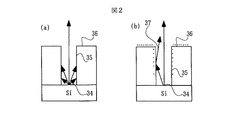
従来の電子線を用いた検査装置でホールパターンの画像を取得すると、例えば電子線の照射エネルギーが500eV(エレクトロンボルト)、アスペクト比が4以下の場合には、開口ホール底からの二次電子信号34は容易に検出され、開口ホールは白く、非開口ホールは黒く観察される。しかし、アスペクト比が高くなると、図2(a)に示す様に、ホール底からの二次電子34は大部分が側壁35によって遮られる。このため、開口ホールも黒く観察されるので非開口ホールを検出することはできなかった。
【0016】
そこで、検査を行なうための二次電子画像を取得する前に、予め電子線等をウエハ表面に照射してウエハ表面36を所望の電圧に帯電させる手段を設けた。図2(b)に示す様にウエハ表面36を正極性に帯電させると、孔底から放出された二次電子34の一部は上方に加速され、効率良く検出可能となる。さらに、孔底から放出された二次電子34を加速できるので、孔底から放出された二次電子34がホール側壁35に衝突したときに、側壁35から二次電子がさらに放出される。側壁35から放出された二次電子のうちの一部37は、開口部に向かって加速されて検出器で検出できるようになる。この結果、高アスペクトホールの孔底から放出された二次電子35を引き出して検出できるようになり、孔底の開口、非開口等の情報を得ることができるようになった。このとき、表面36の帯電電圧に従って、検査可能なアスペクト比や孔径が決定される。そこで、ウエハ表面36を所望の帯電電圧に制御するための手段を設けた。
【0017】
高アスペクトホール底部の開口・非開口を検査するときのウエハ表面36の帯電電圧は、アスペクト比、孔径、ホール周囲の絶縁膜の種類や厚さによって決定される。例えば、シリコン酸化膜に形成されたアスペクト比10のホール底部の開口・非開口を検査するためには、ウエハ表面36を5V以上に帯電させることが必要である。予め記憶されたデータベースに従って、帯電電圧を決定する手段を設けた。本発明では、段差のあるホールパターンに対しては、基板の帯電電圧は5V以上50V以下に設定することが望ましい。
【0018】
ウエハ表面36を所望の正極性の電圧に帯電させるための方法について、次に述べる。ウエハ表面がシリコン酸化膜や有機系材料を用いた絶縁膜の場合、帯電用電子線38として、二次電子放出効率が1以上となる100eV以上1000eV以下の照射エネルギーで電子線を照射する。ウエハ帯電用電子光学系は検査画像を取得する際に照射する電子光学系と兼用することができる。また、ウエハ上面に設置された電極32に最適な電圧をかけることによって、ウエハ上面に電界を生成してウエハ表面36の帯電電圧を制御するための手段を設けた。
【0019】
ウエハ等の大面積を高速で検査するために、ウエハ帯電用電子線38として、画像取得用の電子線よりも空間分解能を落とした電子線を用いることができる。さらに、ウエハ帯電用電子線38の走査方法として、ウエハをいくつかの検査領域に分割し、ウエハの帯電と二次電子画像取得を交互に繰り返すことにより、ウエハの移動時間中にウエハ表面36を効率的に正極性に帯電させて検査するための手段を設けた。
【0020】
次に、負極性の帯電を用いてホールを検査する方法について説明する。図3により、負極性の帯電を用いて欠陥を検出する原理を説明する。表面を負極性に帯電させたとき、図3(a)に示すように正常ホール部40は周りの酸化膜の部分よりも暗く観察される。このとき、非開口の場合は底部に残存する酸化膜41が負極性に帯電し、正常ホールと非開口ホールでは、図3(b)と図3(c)に示すようにホール部の電位分布が異なる。正常ホールでは、孔底と表面36の負極性の帯電電圧の差が大きいので、孔底から放出される二次電子が孔から放出されにくくなる。一方、非開口ホール底41は負極性に帯電しているので、孔底で放出された二次電子は正常ホールよりも検出されやすくなる。検出される二次電子は孔の外周部ほど信号強度が高いので、非開口ホールの二次電子画像41は、図3(a)に示すように正常ホール40よりもホール外周部の信号強度が高くなると同時に、二次電子画像上での孔径は正常ホール40よりも小さく観察される。また、コンタクトホールがテーパー形状となっている場合42は、正常ホール40よりも孔径が大きく観察される。
【0021】
このとき、表面の帯電電圧によって、検査可能なアスペクト比や検出可能な孔底の残膜厚が決定される。そこで、表面を所望の負極性の帯電電圧に制御する手段と二次電子画像中のホールの寸法の相違を検出する手段を設けた。
【0022】
ウエハ表面を所望の負極性の電圧に帯電させる場合には、ウエハ表面がシリコン酸化膜や有機系材料を用いた絶縁膜の場合、このときの電子線照射エネルギーとして、二次電子放出効率が低くなる1000eV以上の電子線を照射する。このとき、画像取得用電子源を用いて、ウエハ表面を負極性に帯電させるのに十分な、大電流を照射する手段を設けた。さらに、効率的にウエハ表面を負極性に帯電させるために、ウエハ上面に設置された電極32に最適な電圧をかけるための手段を設けた。ウエハ上面に生成された電界によって、ウエハ表面から発生した二次電子を効率的にウエハ表面に戻すことが可能となり、画像取得用電子源を用いてウエハ表面を所望の負極性の電圧に帯電させることが可能となった。
【0023】
上述のように、電子線の照射エネルギーとウエハ36上面に設置された電極32の電圧を調整することで、同一の装置でウエハ表面36を任意の正極性および負極性の帯電電圧に制御できるようになった。この結果、半導体装置の回路パターンや材料によらず、種々な半導体回路の検査を高速にできるようになった。
【0024】
次に、ウエハ表面の帯電電圧を正極性、あるいは負極性の所望の電圧に制御する方法について述べる。照射条件調整用のチップに移動し、帯電用電子線を走査・照射後、画像取得用電子線を走査・照射し、二次電子画像を取得する。二次電子画像を取得する際に、エネルギーフィルター13を用いて二次電子を検出する。このエネルギーフィルターとして、ある閾値以上、あるいは、ある閾値以下の二次電子を検出するエネルギーフィルターを用いることができる。
【0025】
ある閾値以上の二次電子を検出するエネルギーフィルターを用いて画像を取得する場合は、エネルギーフィルター13のフィルター電圧を固定させて二次電子画像を取得した後、プリチャージと二次電子画像を取得する場所を移動し、エネルギーフィルターの閾値を2つめの値に固定して二次電子画像を取得することを繰り返すことによって、ウエハ表面の帯電電圧を自動的に計測する手段を設けた。
【0026】
帯電電圧を計測する別の手法として、エネルギーフィルター13のフィルター電圧をスキャンさせながら二次電子画像を取得し、得られた二次電子画像から帯電電圧を計測することもできる。これらの方法を用いて帯電電圧を計測し、ウエハ表面が所望の帯電電圧になるように、帯電用電子線のエネルギー、電流値、電極電圧を最適化する手段を設けた。さらに、二次電子画像を取得するときの電子線の照射条件を最適化する手段を設けた。
【0027】
帯電用電子線と二次電子画像取得用電子線の調整後、実際に検査を行なうが、検査時に二次電子画像を取得する際には、通常はエネルギーフィルター13を用いないで二次電子画像の取得が可能である。しかし、特定の場合について、エネルギーフィルター13を用いて二次電子画像を取得するための手段を設けた。エネルギーフィルターの設定値は、上述した帯電電圧計測時に取得した二次電子画像から、最適化を行なうための手段を設けた。二次電子エネルギーをフィルタリングして画像を取得することによって、高感度に欠陥を検出することが可能となる。
【0028】
これらの手法を用いて二次電子画像を取得後、ウエハ上の別の領域で取得した同一パターンの二次電子画像とを比較して、欠陥を検出するための機構を設けた。さらに、ホール部のコントラストとホールの寸法を算出する機構を設け、欠陥ホールのコントラストと寸法から、欠陥の種類を自動判定するための機構を設けた。さらに、これらの欠陥の判定結果と欠陥のウエハ面内分布を画面上に表示する手段を設けた。
【0029】
まず、正極性の帯電をさせたときに取得した二次電子画像から、欠陥を検出する方法について述べる。ウエハ表面を正極性に帯電させた場合、正常ホールの二次電子画像は明るく観察される。非開口の場合は、底部に残存する酸化膜が帯電するため、正常ホールよりも暗く観察される。また、コンタクトホールがテーパー形状となっている場合は、ホール部は明るく、大きく観察される。コントラストとホール寸法の相違から、欠陥ホールを判定し、欠陥の種類を自動判定する手段を設けた。さらに、底部に残存する酸化膜の厚さが厚いほど、欠陥ホール部は暗く観察される。欠陥ホール部の明るさから、底に残存する膜厚を算出するための手段を設けた。
【0030】
一方、ウエハ表面を正極性に帯電させて半導体回路のショート欠陥を検出する手法が提案されている。本発明によって、ウエハ表面を正極性に帯電させてホールの非開口検査が可能となった結果、半導体回路のショート欠陥と非開口欠陥とを同一の装置で検査できるようになった。
【0031】
次に、ポリSiマスクの様にウエハ表面が正極性に帯電しにくい材料の場合、あるいは、孔底の材料が絶縁膜のように電流を流さない材料である場合に、欠陥を検出する方法について述べる。このようなウエハ表面は正極性に帯電させた場合、正常ホールの二次電子画像は暗く観察される。非開口の場合、正常ホールと非開口ホールでは、開口部の電界が変化することによって、正常ホールよりも小さく観察される。ホール寸法の相違から、欠陥ホールを判定し、欠陥の種類を自動判定する手段を設けた。欠陥ホールの寸法から、底に残存する膜厚を算出するための手段を設けた。
【0032】
さらに、ウエハ表面を負極性に帯電させた場合に取得した二次電子画像から、欠陥を判定する方法について述べる。ウエハ表面を負極性に帯電させた場合、正常ホールの二次電子画像は暗く観察される。非開口の場合は、底部に残存する酸化膜が帯電し、開口部の電界が変化することによって、正常ホールよりも小さく観察される。また、コンタクトホールがテーパー形状となっている場合は、正常ホールよりも大きく観察される。ホール寸法の相違から、欠陥ホールを判定し、欠陥の種類を自動判定する手段を設けた。欠陥ホールの寸法から、底に残存する膜厚を算出するための手段を設けた。
【0033】
この結果、ホールパターンの開口・非開口等の欠陥の有無を高速に検査することが可能となる。さらに、検出した欠陥情報から、半導体装置の製造工程における製造条件を微調整する機構を設けた。この機構によって、欠陥の種類とウエハ面内分布から、欠陥発生要因を推定し、半導体装置を製造する条件を微調整することが可能となった。さらに、検出した欠陥情報から、半導体装置の欠陥を減少させる処理を半導体製造工程に追加する機構を設けた。これにより、孔底の非開口等の得られた欠陥情報から半導体製造プロセスの最適化を早期に行なうことができる。また、欠陥の種類や欠陥のウエハ面内分布から、プロセス異常を早期に発見し、欠陥発生要因の推定を早期に行なうことが可能となり、半導体装置の信頼性を高めることが可能になる。
【0034】
【発明の実施の形態】
以下、本発明の実施例を、図面を参照して説明する。
【0035】
(実施例1)
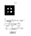
本実施例では、ドライエッチング後のホールパターンの検査方法、及び装置の一例について説明する。本実施例における半導体装置の検査装置の構成を図1に示す。
【0036】
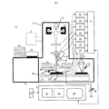
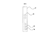
半導体装置の検査装置1は、電子光学系2、ステージ機構系3、ウエハ搬送系4、真空排気系5、光学顕微鏡6、制御系7、操作部8より構成されている。電子光学系2は、電子銃9、コンデンサレンズ10、対物レンズ11、検出器12、エネルギーフィルター13、偏向器14(例えば、EXB偏向器)、ウエハ上面の電極32、ウエハ高さ検出器15より構成されている。ステージ機構系3は、XYステージ16およびウエハを保持し載置するためのホルダ(試料台)17、ホルダ17およびウエハ18に負の電圧を印加するためのリターディング電源19より構成されている。XYステージ16には、レーザ測長による位置検出器が取りつけられている。ウエハ搬送系4はカセット載置部20とウエハローダ21とXYステージ16間をウエハ18が行き来するようになっている。制御系7は、信号検出系制御部22、ブランキング制御部23、ビーム偏向補正制御部24、電子光学系制御部25、ウエハ高さセンサ検出系26、ステージ制御部27、電極制御部33より構成されている。操作部8は、操作画面および操作部28、画像処理部29、画像・検査データ保存部(記憶部)30、外部サーバ31より構成されている。
【0037】
欠陥検出方法について、検査フローに従って説明する。図4に、検査フローを示す。まず、操作画面28上で検査するウエハのカセット内棚番号を指定する(ステップ43)。そして、被検査ウエハの情報として、アスペクト比、ホール径、パターンを形成する材料等の情報を入力する。さらに、帯電用電子線38の照射条件として、電子ビーム照射エネルギー、ビーム電流、ビーム径等の条件を入力し、ウエハ表面の帯電電圧を指定する。さらに検査条件として、検査領域、二次電子画像を取得するときの電子ビーム照射エネルギー、ビーム電流、走査速度、走査サイズを入力する(ステップ44)。また、被検査ウエハの情報から、データベース化された検査条件を用いることもできる。これらの被検査ウエハの情報、電子線の照射条件、検査条件は、外部サーバ31から入力することも可能である。
【0038】
ウエハ表面を正極性に帯電させるときの電子ビーム照射条件として、例えば照射エネルギーは電子線放出効率が1以上となる100eV以上1000eV以下の値に設定することができる。検査時の照射エネルギーは、ウエハ帯電用電子線と同じ値に設定することが望ましい。検査時の照射エネルギーとウエハ帯電用電子線の照射エネルギーを同程度にすることによって、一つの電子源を用いて、ウエハを帯電させるための電子線と二次電子画像取得時の電子線が照射可能となった。また、比較的低エネルギーの電子線を照射することによって、ウエハ表面を正極性に帯電させるだけでなく、半導体装置に与えるダメージを低減させて検査を行なうことが可能となった。
【0039】
ウエハの帯電電圧の設定値は、主としてホールパターンのアスペクト比から決定される。図5にホール部の二次電子画像の明るさの帯電電圧依存性を示す。アスペクト比4までのホール底からの二次電子は、帯電電圧が5V以下であっても取得可能であるが、アスペクト比8以上になると、図5に示すように10V以上に帯電させる必要がある。予め取得した必要な帯電電圧のアスペクト比依存性のデータベースから、帯電電圧の設定値を決定することもできる。検査条件の設定が完了したら検査を開始する。上記の検査条件の設定は、オフラインのコンピュータを用いて予め設定することもできる。
【0040】
検査を開始すると、ウエハ18を検査装置に搬送する。ウエハ18はカセットからウエハローダ内に搬送された後、ウエハローダは真空排気される。その後、既に真空排気されている検査室に導入される(ステップ45)。
【0041】
ウエハロード終了後、上記入力された検査条件に基づき、電子光学系制御部25より各部に二次電子画像取得時の電子線照射条件が設定される。そして、ウエハホルダ17上にビーム校正用パターンが電子光学系2下に来るようにステージ16が移動する(ステップ46)。その後、電子線画像を取得し、焦点、非点および検出系の設定を調整して画像のコントラスト等を調整する(ステップ47)。同時にウエハ18の高さを高さ検出器15より求め、ウエハ高さ検出系26によって高さ情報と電子ビームの合焦点条件の相関を求め、この後の電子線画像取得時には毎回焦点合わせを行なうことなく、ウエハ高さ検出の結果より合焦点条件に自動的に調整することができる。
【0042】
二次電子画像取得時の画像調整が完了したら、帯電用電子線38の照射条件の調整を行なう(ステップ48)。まず、帯電電圧調整用パターンが電子光学系2下に来る様にステージ16が移動する。帯電用電子線38のビーム径は二次電子画像取得用ビームよりも100倍から1000倍程度大きなビームを使用することができる。
【0043】
図6に、帯電用電子線38と二次電子画像取得ビームのスキャン方式の一例を示す。帯電用電子ビームを第一の領域57に一列照射後、二次電子画像取得用電子ビームを走査させながら第一の領域に含まれる第二の領域58の二次電子画像を取得する。第一の領域57は、第二の領域を含む十分広い領域58である。このとき、二次電子画像は、エネルギーフィルター13を用いて取得する。
【0044】
一例として、ある閾値以上の二次電子を取得する方式のエネルギーフィルターを用いた。このエネルギーフィルターでは、フィルターにかける電圧以上のエネルギーを持つ電子が検出される。まず、閾値V0に設定して上記第二の領域58の二次電子画像を取得する。この二次電子画像のホール部と酸化膜の部分の信号強度をメモリ30に記憶する。次に、第一の領域57に含まれ、第二の領域を含まない第三の領域59の二次電子画像を取得する。このとき、エネルギーフィルター13は閾値V1に設定する。この二次電子画像のホール部と酸化膜の部分の信号強度をメモリ30に記憶する。酸化膜の部分の信号強度が変化するフィルター電圧が求まるまで、第一の領域58に含まれる第nの領域60の二次電子画像をフィルター電圧Vnで取得する上記の過程を繰り返す。
【0045】
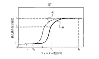
このときのフィルター電圧Vnの設定方法について、図7を用いて説明する。ある電圧に帯電した酸化膜からの信号61は、フィルター電圧によって図7のように変化する。V0では、全てのエネルギーの二次電子が取得されるので信号強度は最大値I0である。V1ではほとんどの二次電子が検出されないので、信号強度は最小値I1である。V0とV1の値を、例えば50Vから−20Vの範囲で設定する。さらに、V2からViまでの値はV0とV1の間を、例えば10V間隔で設定する。信号強度が(I0+I1)/2以上I0以下となった場合、例えば5V間隔でさらに2点設定される。信号強度がI1以上(I0+I1)/2以下となった場合、Vn+5VがVn+1として設定される。これらの信号強度から、(I0+I1)/2となるVmを求めることができる。ウエハの帯電電圧は、予め取得してある基板Siからの信号強度62のフィルター電圧依存性の曲線からのシフト量から計算される。
【0046】
このようにして帯電電圧を計測しながら、所望の帯電電圧が得られるまで、帯電用電子ビームの調整を行なう(ステップ49)。このような方法を用いて帯電電圧を計測し、ウエハ表面が所望の帯電電圧になるように、帯電用電子線38の電流値、電極電圧32、およびビームエネルギーを最適化する手段を設けた。
【0047】
ここで、実際に検査を行なうときに、エネルギーフィルター13を使用して検査を行なうことも可能である。検査時のフィルター電圧の設定値を帯電電圧測定時に決定することが可能である。フィルター電圧の設定値の決定方法について説明する。帯電電圧測定の際に取得した二次電子画像から、酸化膜からの信号強度ISiO2とホール部からの信号強度IHoleを算出する。
【0048】
図8に、酸化膜の信号強度64とホール部からの信号強度63のフィルター電圧による依存性を示す。さらに、コントラストC=(IHole−ISiO2)/ISiO2を算出し、これが最大となるフィルター電圧VMAXを検査時の設定値に決定する。決定された設定値は、メモリ30に記憶される。
【0049】
その後、電子線照射条件39および画像調整が完了したら、ウエハ18上の2点からアライメントを行なう(ステップ50)。被検査ウエハ18は予め登録された光学顕微鏡6下の、所定の第一の座標に配置され、操作画面28内のモニタに被検査ウエハ18上に形成された回路パターンの光学顕微鏡画像が表示され、位置回転補正用に予め記憶された同じ位置の同等回路パターンの光学顕微鏡画像と比較され、第一の座標の位置補正値が算出される(ステップ51)。
【0050】
次に、第一の座標において、光学顕微鏡画像から電子線画像に切り替える。光学顕微鏡6と電子光学系2は所定の距離が離れた位置に配置されており、該距離は既知のパラメータとして装置内に記憶されているため、光学顕微鏡画像と電子線画像は任意に切り替えすることができる。電子線画像についても、光学顕微鏡画像と同様に予め位置回転補正用に回路パターンの画像を記憶してあり、該記憶された電子線画像と取得した電子線画像とを比較することにより、光学顕微鏡より精密な第一の座標の位置補正値が算出される。
【0051】
次に、第一の座標から一定距離離れ第一の座標と同等の回路パターンが存在する第二の座標に移動し、同様に光学顕微鏡画像が取得され、位置回転補正用に記憶された回路パターン画像と比較され、第二の座標より位置補正値および第一の座標に対する回転ずれ量が算出される。さらに、第二の座標においても同様に電子線画像に切り替え、予め記憶された回路パターンの電子線画像と比較され、精密な第二の座標の位置補正値が算出される。この算出された回転ずれ量および位置ずれ量に基づき、制御部25および電子ビーム偏向信号補正部24において電子ビームの走査偏向位置は回路パターンの座標に対応するように補正される。
【0052】
このようにして、被検査ウエハ18のアライメントが完了したら、被検査ウエハ18に帯電用電子線38を照射後、電子線画像を取得し、明るさの調整を実施する(ステップ52)。検査条件ファイルに基づき、電子線画像を取得する際には電子ビーム電流や電子ビーム照射エネルギー、エネルギーフィルター13に印加する電圧や使用する検出器12、検出系のゲインが設定されており、これらのパラメータを設定して電子線画像を取得する。
【0053】
この明るさ調整が完了したら、検査を実行する(ステップ53)。検査領域は、検査条件ファイルに予め指定しておく。ウエハ帯電用電子線38を照射する場合、ウエハをいくつかの検査領域に分割し、ウエハの帯電と二次電子画像取得を交互に繰り返すことにより、ウエハの移動時間中にウエハ表面を効率的に正極性に帯電させることができる。
【0054】
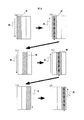
図9に、電子線の走査方法の一例を示す。まず、第一の照射領域66にウエハ帯電用電子線38を設定済みの条件で、図9(a)のように照射し走査させる。次に、第一の走査領域67に画像取得用電子線39を、図9(b)で示すように走査させて、二次電子画像を取得する。次に、図9(c)に示す様に、第二の照射領域68にウエハ帯電用電子線38を照射し、第二の走査領域69に画像取得用電子線39を走査する。このとき、ウエハを移動させながら帯電用電子線38を照射することができる。このように、ウエハの移動時間中に帯電用電子線38を照射できるので、ウエハを帯電させるための余分な時間をかけることなく、検査することが可能となった。
【0055】
図9に示すように、上記の操作を繰り返すことによって、ウエハ全面を検査することができる。検査時には、XYステージ16を連続的に移動しながら電子ビームを被検査ウエハ18の所定の領域に照射し、電子線画像を逐次形成しながら画像信号を記憶部30に記憶された信号と比較しながら、記憶部30に逐次画像を記憶する。かかる検査においては、予め検査条件ファイル204により検出器12は設定されている。検出器12の前方に配置されているエネルギーフィルター13に電圧を印加することもできる。
【0056】
次に、ホールの欠陥判定方法について説明する。例えば膜材料がシリコン酸化膜(SiO2)の場合、二次電子画像取得後、以下の方法で欠陥判定を行う。
【0057】
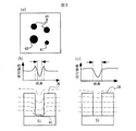
図10に、コンタクトホールを形成したパターンの二次電子画像(a)と欠陥判定フロー(b)の一例を示す。図10(a)に示す非開口ホール71は、開口ホール70よりも暗く観察される。一方、テーパー形状となった欠陥ホール72は、開口ホール70よりも明るく、孔の寸法は大きく観察される。
【0058】
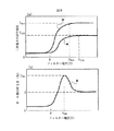
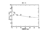
図11には、ホール部のコントラストの残膜厚依存性を示す。残膜厚0は、開口ホールのコントラストを示している。非開口ホール71は、開口ホール70よりも暗く観察されることから、非開口ホール71を欠陥と判定することが可能である。このとき、非開口ホール71のコントラストは残膜厚に従って暗くなることから、ホール部のコントラストから、非開口ホールの残膜厚を推定することも可能である。
【0059】
取得された二次電子画像から欠陥判定は、以下のように行なう。まず、図10(b)に示すように、二次電子画像の形状を比較し(ステップ73)、参照する二次電子画像と形状が一致しない場合、形状異常と判定される。さらに、ホール部のコントラストを参照する二次電子画像と比較する(ステップ74)。参照画像とコントラストが同程度の場合、正常ホールと判定される。参照画像よりもホール部の明るさが暗い場合、エッチ残り、あるいはホール内異物有りと判定される。ホール部のコントラストが参照画像よりも明るい場合はテーパー形状と判定される。これにより、非開口ホール71を非開口欠陥、テーパー形状のホール72をテーパー形状と判定される。
【0060】
さらに、記憶部30、あるいは外部サーバ31に予め記憶してあるデータから、非開口ホールのコントラストから残膜厚を推定(ステップ75)することも可能である。残膜厚によるコントラストの変化のデータベースとして、ホールのアスペクト比、ホール径、帯電電圧、絶縁膜材料等のパラメータに従って、検索可能である。
【0061】
被検査ウエハ上に、コンタクト底に異なる種類の接合が含まれている場合がある。このとき、開口ホール底の抵抗は接合の種類によって異なるので、ホールの明るさは接合の種類で変化する。このような場合、ウエハ上のパターン配置情報から、同一種類のパターン同士を比較することによって、同一種類の接合を持つホール同士を比較検査する。特に、コンタクト底にn拡散層が上層にあるpn接合が形成されている場合、ホールからのコントラストは低くなる。
【0062】
図12に、pn接合を形成した場合のモデル図を示す。図中、76は層間絶縁膜、77はn拡散層、78はpウエル、79はシリコン基板、80は一次電子線である。
【0063】
pn接合が無いホール底では、電子線放出効率が1以上の条件で電子線が照射されたとき、基板から電子が供給されるため、孔底の電圧は0Vとなる。しかし、n拡散層77上に電子線が照射されると、pn接合のために基板79側から電子は供給されず、孔底が帯電するため、コントラストは低くなる。このような場合、電子ビームエネルギーを最適化することによって、コントラスト向上が可能となる。
【0064】
例えば、接合深さがL、接合領域に幅Wの空乏層領域が形成された場合について説明する。電子の侵入深さRは,試料の原子量(A)、原子番号(Z)、密度(ρ)が決定されると、電子のエネルギーで決定される。例えば、入射エネルギー500eVの電子線がSiに照射された場合、電子線の侵入深さRは10〜20nmとなる。電子線のエネルギーが高い程電子の侵入深さRは深くなる。電子線の侵入深さRが浅く、空乏層領域まで電子が侵入しない場合、n拡散層77上に電子線80が照射されると表面は正に帯電する。ここで、電子線の照射エネルギーと表面の帯電電圧を調整して、空乏層内に電子線が侵入するようになると、空乏層内に電子-正孔対が生成されるので、接合の抵抗が下がる。この結果、基板79から電子が供給されるので、孔底の帯電は抑制されて、ホール部の二次電子コントラストを向上させることができる。
【0065】
また、被検査ウエハ表面にPoly Siマスク等の導電性の材料を使用した場合がある。このとき、ウエハ表面を5V以上に帯電させることは困難である。一方、孔底がSiNのような絶縁膜の場合や接合の抵抗が高く、コンタクト底に電流が供給されにくい場合がある。このとき電子線照射によって孔底は帯電するので、孔底から放出された二次電子を引き上げて検出することは困難である。
【0066】
このような場合について、非開口の検査方法を説明する。ウエハ表面に電子線を照射すると、ウエハ表面が正極性に帯電した場合でも、図3に示す様に、正常ホール40の二次電子画像は暗く観察される。非開口の場合は、底部に残存する膜41が正常ホール40の底よりも帯電し、開口部の電界が変化することによって、正常ホールよりも小さく観察される。また、欠陥ホールの寸法は、底に残存する膜厚が厚くなるに従って小さく観察される(図3中、41)。コンタクトホールがテーパー形状となっている場合は、正常ホールよりも大きく観察される(図3中、42)。観察された二次電子画像のホール寸法の相違から、欠陥ホールを判定し、欠陥の種類を自動判定する手段を設けた。予め記憶してあるホール寸法と欠陥ホールの関係から、欠陥ホールの寸法から、底に残存する膜厚を算出するための手段を設けた。
【0067】
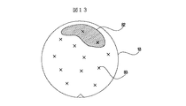
以上述べたような方法を用いて欠陥と判定された箇所は、欠陥箇所の座標、信号値、欠陥の種類および欠陥のサイズ等が自動的に記録され、図13に示すように、操作画面28内のウエハマップ上の相当する箇所に欠陥有りのマークが種類別に表示される。該検査条件ファイルで指定された領域の検査を終了したら、欠陥箇所を再度画像取得することができる(図4中、ステップ54)。
【0068】
以上述べたように、ウエハ表面を正極性に帯電させてホールの非開口の検査が可能となった。一方、正極性の帯電を用いて半導体回路のショート欠陥を高速に検出する手法が提案されている。これによって、同一の検査装置を用いて、ホールの非開口とショート欠陥を高速・高感度に検出することが可能となった。さらに、本検査装置を用いて、実施例2で後述するように、電子線照射エネルギーとウエハ表面に設置された電極電圧を調整して、所望の負極性の帯電電圧に制御することにより、同一の装置でウエハ表面を所望の正極性と負極性の帯電電圧に制御することが可能となった。これによって、半導体装置の回路パターンの種類や材料によらず、様々な種類の半導体回路の欠陥を検出できるようになった。
【0069】
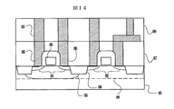
図14に、本発明により検査されるホールパターンを持つ半導体装置の一例として、DRAMの断面略図を示す。フィールド酸化物層83によって半導体基板84上に形成された活性領域は分割されている。活性領域の上方にはゲート電極85が形成され、スペーサー86によって覆われている。酸化膜等の第1絶縁層87が表面に形成された後、第1のコンタクトホール88がドライエッチングによって形成される。その後、コンタクトホール88はビット線用のダイレクトコンタクトとして形成される。次に、ビット線を形成した後、第2絶縁層89が形成され、第2のコンタクトホール90が形成される。本発明による検査の一例として、図14に示したDRAM製造プロセス中のダイレクトコンタクトホール88や配線上に形成されたホール89について検査が行なわれる。さらに、他の配線上に形成されたホールについても検査を行なうことができる。あるいは、これらのホールパターンを形成するためのマスクパターンの現像プロセス後に行なうこともできる。なお、図中、91はp拡散層、92はn拡散層、93はNウエル、94はPウエル、95は半導体基板である。
【0070】
以上示したように、コンタクトホールパターンを含むウエハを検査することが可能となり、欠陥の自動判定が可能となった。さらに、欠陥の種類およびウエハ面内分布から、いくつかの欠陥発生要因については、予め作成してあるデータベースから自動的に欠陥発生プロセスや要因を特定する機構を設けた。さらに、欠陥発生プロセスの加工条件を微調整する機構を設けた。また、検出された欠陥情報から、非検査ウエハに追加処理を行なうことによって、被検査ウエハ上の欠陥を低減させるための機構を設けた。
【0071】
例えば、検査結果から半導体製造プロセス条件を微調整する機構の一例を述べる。ウエハ上に同心円状、あるいは、全面に非開口欠陥が多発している場合、非開口欠陥の残膜厚によって、ホール加工を行なうドライエッチ時間を微調整することができる。特定パターンに非開口欠陥やテーパー状の欠陥が発生している場合は、リソグラフィー条件の微調整やレチクルの交換を行なう。半導体メモリマットの周囲等、パターンの粗密によって欠陥が多発する場合は、ドライエッチのガス流量の微調整やエッチャーのクリーニング等を行なう。異物が多発している場合は、半導体製造装置のクリーニングやドライエッチ条件の微調整を行なう。
【0072】
一方、被検査ウエハには欠陥を低減できる処理を追加する機構を設けた。ドライエッチ不足による非開口が多発している場合は、ドライエッチを追加することができる。異物が多発している場合は洗浄の追加を行なうことができる。この結果、発生のプロセスやその要因を早期に特定することができるようになり、ドライエッチングプロセスを始めとする半導体製造プロセスへのフィードバックを早期に行うことが可能となった。
【0073】
(実施例2)
本実施例では、ドライエッチング後のホールパターンの検査方法、及び装置の一例として、酸化膜表面を負極性に帯電させて検査する方法について説明する。本実施例では、図1に示した半導体検査装置を用いることができる。
【0074】
ウエハ表面36を所望の負極性の電圧に帯電させる場合には、ウエハ表面36がシリコン酸化膜や有機系材料を用いた絶縁膜の場合、このとき、ウエハ帯電用電子線照射エネルギーとして、二次電子放出効率が1以下となる1000eV以上の電子線を照射する。画像取得用電子線39の照射エネルギーは、ウエハ帯電用電子ビームと同じ値に設定することが望ましい。検査時の照射エネルギーとウエハ帯電用電子ビームの照射エネルギーを同程度にすることによって、一つの電子源を用いて、ウエハを帯電させるための電子線と二次電子画像取得時の電子線が照射可能となった。さらに、効率的にウエハ表面を負極性に帯電させるために、ウエハ上面に設置された電極32に最適な電圧をかける。
【0075】
これらのビームエネルギー、ビーム電流、電子線照射時間等の電子ビーム照射条件、電極電圧の設定方法について説明する。あるいは、これらの設定値は予め記憶してある検査条件データファイルから読み込むこともできる。まず、ウエハの帯電電圧の設定値は、主としてホールパターンのアスペクト比から決定される。
【0076】
図4に示した検査フローにおいて、ウエハロード(ステップ45)終了後、所望の負極性の帯電電圧を満たすように、電子線照射条件の設定を行なう方法について説明する。一例として、ある閾値以上の二次電子を取得する方式のエネルギーフィルターを用いて二次電子画像を取得し、帯電電圧を計測する方法を用いた。まず、帯電電圧調整用パターンが電子光学系2下に来る様にステージ16が移動する。そこで、閾値V0に設定して第一の領域の二次電子画像を取得する。この二次電子画像のホール部と酸化膜の部分の信号強度を記憶部30に記憶する。
【0077】
次に、エネルギーフィルターは、閾値V1に設定して第二の領域の二次電子画像を取得する。この第二の領域の二次電子画像のホール部と酸化膜の部分の信号強度を記憶部30に記憶する。酸化膜の部分の信号強度61が変化するフィルター電圧が求まるまで、第一の領域に含まれる第nの領域の二次電子画像をフィルター電圧Vnで取得する上記の過程を繰り返す。このときのフィルター電圧Vnの設定方法は、一例として、実施例1で述べた方法を用いることができる。これらの信号強度から、(I0+I1)/2となるVmを求めることができる。
【0078】
ウエハの帯電電圧は、予め取得してある基板Siからの信号強度のフィルター電圧依存性の曲線からのシフト量から計算される。電子ビーム照射条件を変えて帯電電圧を繰り返し計測し、所望の帯電電圧が得られるまで、電子ビームの調整を行なう。このような方法を用いて帯電電圧を計測し、ウエハ表面が所望の帯電電圧になるように、ウエハ帯電用電子線および画像取得用電子線の電流値、照射時間、ビームエネルギー、電極電圧を最適化する手段を設けた。
【0079】
その後、電子線照射条件および画像調整が完了したら、ウエハのアライメント(ステップ50)、キャリブレーション(ステップ51)、明るさの調整(ステップ52)を行ない、検査を実行する(ステップ53)。検査に使用する二次電子画像取得時には、検出器12の前方に配置されているエネルギーフィルター13に電圧を印加して、検出感度を向上させることもできる。
【0080】
次に、ホールの欠陥判定方法について説明する。ウエハ表面を負極性に帯電させた場合、図3に示す様に、正常ホール40の二次電子画像は暗く観察される。非開口ホール41の場合は、底部に残存する酸化膜が帯電し、開口部の電界が変化することによって、正常ホールよりも小さく観察される。また、非開口ホール41のような欠陥ホールの寸法は、底に残存する膜厚が厚くなるに従って小さく観察される。コンタクトホールがテーパー形状(42)となっている場合は、正常ホールよりも大きく観察される。観察された二次電子画像のホール寸法の相違から、欠陥ホールを判定し、欠陥の種類を自動判定する手段を設けた。予め記憶してあるホール寸法と欠陥ホールの関係から、欠陥ホールの寸法から、底に残存する膜厚を算出するための手段を設けた。
【0081】
被検査ウエハ上に、コンタクト底に異なる種類の接合が含まれている場合がある。このとき、開口ホール底の抵抗は接合の種類によって異なるので、ホールの寸法は接合の種類で変化する。このような場合、ウエハ上のパターン配置情報から、同一種類のパターン同士を比較することによって、同一種類の接合を持つホール同士を比較検査する。
【0082】
検査によって欠陥と判定された箇所は、その欠陥箇所の座標、信号値、欠陥の種類および欠陥のサイズ等が自動的に記録される。図13は、上記検査を行った結果を示したものである。本検査では、ウエハ18上に非開口欠陥の分布82と形状異常欠陥の分布83が検出された。操作画面28内のウエハマップ上の相当する箇所に欠陥有りのマークが表示され、分類結果に基づき種類別にマークが表示されている。検査条件ファイルで指定された領域の検査を終了したら、欠陥箇所を再度画像取得することができる(図4中、ステップ54)。
【0083】
以上示したように、ウエハ上を負極性に帯電させてコンタクトホールパターンを含むウエハを検査することが可能となり、欠陥の自動判定が可能となった。この結果、第一の実施例で示したような正極性の電圧に帯電することが困難な材料や回路パターンを持つ被検査ウエハの検査も可能となった。
【0084】
このように、これらの実施例による方法を用いることによって、様々な種類のパターンにおいて、ドライエッチング工程後にホールパターンの開口・非開口等の欠陥の有無を非破壊で高速に検査することが可能となった。非破壊で深孔底の開口性の評価が可能となった結果、製造工程途中で抜き取ったウエハの検査終了後、続きの工程にウエハを戻して半導体を製造することが可能となった。また、配線工程の前に開口性の検査が可能となったことによって、ドライエッチングプロセス開発期間を大幅に短縮できるようになった。さらに、欠陥の種類、ウエハ面内分布や欠陥の位置を高速に得られるようになり、プロセス異常を早期に発見し、欠陥発生要因の推定を短期間に容易にできるようになった。
【0085】
なお、以上の実施例では、電子線による場合について説明してきたが、本発明では、電子線以外の荷電粒子線、例えばイオンビームによっても適用可能である。
【0086】
【発明の効果】
本発明によれば、ホールパターン等の段差の大きいパターンを有する半導体ウエハ等の基板の欠陥検査を高速、かつ高精度に行うことが可能な基板検査装置および基板検査方法を実現できる。特に、半導体装置製造プロセスにおけるプロセス開発期間および歩留まり向上期間を大幅に短縮できるようになり、半導体装置の信頼性および生産性を高めることが可能となった。
【図面の簡単な説明】
【図1】本発明の半導体検査装置の一例を示す構成図。
【図2】本発明で用いた孔底から発生した二次電子検出原理の説明図。
【図3】本発明で用いた負極性の帯電による欠陥検出原理の説明図。
【図4】本発明における検査フローの一例を示す図。
【図5】ホール部の二次電子画像の明るさの帯電電圧依存性を示す図。
【図6】ビームスキャン方式の一例を示す説明図。
【図7】フィルター電圧の設定方法の一例を示す図。
【図8】酸化膜の信号強度とホール部の信号強度のフィルター電圧依存性を示す図。
【図9】ビームスキャン方式の一例を示す説明図。
【図10】コンタクトホールパターンの二次電子画像(a)と欠陥判定フロー(b)の一例を示す図。
【図11】ホールパターンのコントラストの残膜厚依存性を示す図。
【図12】pn接合を形成した場合の説明図。
【図13】ウエハマップ上に表示した欠陥分布の一例を示す図。
【図14】本発明により検査されるホールパターンを有する半導体装置の一例を示す断面略図。
【符号の説明】
1…検査装置、2…電子光学系、3…ステージ、4…ウエハ搬送系、5…真空排気系、6…光学顕微鏡、7…制御系、8…操作部、9…電子銃、10…コンデンサレンズ、11…対物レンズ、12…検出器、13…エネルギーフィルター、14…偏向器、15…高さセンサ、16…XYステージ、17…ウエハホルダ、18…ウエハ、19…リターディング電源、20…ウエハカセット、21…ウエハローダ、22…信号検出系制御部、23…ブランキング制御部、24…ビーム偏向補正部、25…電子光学系制御部、26…高さ検出系、27…ステージ制御部、28…操作画面、29…画像処理部、30…データ保持部、31…外部サーバ、32…電極、33…電極制御部、34…孔底からの二次電子、35…側壁、36…ウエハ表面、37…側壁から放出された二次電子、38…ウエハ帯電用電子線、39…画像取得用電子線、40…正常ホール、41…非開口ホール、42…テーパー形状のホール、43…ウエハセット、44…検査条件入力、45…ロード、46…ステージ移動、47…ビーム校正、48…帯電用電子ビーム調整、49…ビーム補正、50…アライメント、51…キャリブレーション、52…調整、53…検査、54…画像取得、55…結果出力、56…アンロード、57…第一の領域、58…第二の領域、59…第三の領域、60…第nの領域、61…酸化膜からの信号、62…基板Siからの信号、63…ホール部の信号強度、64…周囲の酸化膜の信号強度、65…コントラスト、66…帯電用電子ビームの第1の照射領域、67…画像取得用ビームの第1の走査領域、68…帯電用電子ビームの第2の照射領域、69…画像取得用ビームの第2の走査領域、70…開口ホール、71…非開口ホール、72…テーパー形状のホール、73…形状比較、74…コントラストの比較、75…残膜厚の推定、76…層間絶縁膜、77…n拡散層、78…pウェル、79…シリコン基板、80…一次電子線、81…電子の飛程、82…非開口欠陥の分布、83…形状異常欠陥の分布、84…フィールド酸化物層、85…ゲート電極、86…スペーサー、87…第1絶縁層、88…第1のコンタクトホール、89…第2絶縁層、90…第2のコンタクトホール、91…p拡散層、92…n拡散層、93…Nウエル、94…Pウエル、95…半導体基板。[0001]
BACKGROUND OF THE INVENTION
The present invention relates to a substrate inspection technique using a charged particle beam, and in particular, detects foreign matters and defects on a substrate such as a semiconductor wafer having a fine circuit pattern in the inspection technique using a charged particle beam such as an electron beam. Related to inspection technology.
[0002]
[Prior art]
As a method for evaluating a semiconductor wafer having a fine circuit pattern using an electron beam, a technique for performing high-throughput and high-precision inspection in response to an increase in wafer diameter and circuit pattern miniaturization has been put into practical use. For example, as disclosed in Japanese Patent Application Laid-Open No. 06-139985, a method is known in which defect inspection is performed using the contrast of a secondary electron beam caused by a surface potential difference.
[0003]
In addition, as a method of evaluating electrical defects from potential contrast, potential contrast is obtained by irradiating an electron beam before inspection and precharging the wafer surface in advance to a positive or negative polarity before acquiring a secondary electron image. Can be increased. For example, as disclosed in Japanese Patent Application Laid-Open No. 2000-208085, as a method of charging to positive polarity, in pattern inspection of a contact hole or the like in which a plug is embedded, an electron beam is irradiated on the wafer surface, and then the potential contrast is increased. The method of obtaining is known.
[0004]
However, these descriptions describe the inspection method for the circuit in which the plug is embedded, but there is no description regarding the inspection method for the bottom of a pattern having a very large step such as a hole after dry etching.
[0005]
On the other hand, a technique is known in which the bottom of a hole pattern can be observed from a secondary electron image emitted when the hole pattern is irradiated with an electron beam. However, since these conventional scanning electron microscopes observe a limited field of view at a high magnification over time, it has been impossible to inspect the entire surface of the wafer for defect inspection.
[0006]
As a method for inspecting the non-opening of the contact hole by charging the wafer surface to a negative polarity, in Japanese Patent Laid-Open No. 06-139985, the wafer is irradiated with a low acceleration electron beam before acquiring a secondary electron image. The surface is negatively charged. In this method, when there is a residual film at the bottom of the hole, the non-opening is evaluated by utilizing the fact that the potential of the opening changes due to the residual film and the apparent hole diameter becomes small.
[0007]
However, in this method, since a limited visual field is observed over time at a high magnification, it has been impossible to perform defect inspection by observing the entire surface of the wafer. In addition, in order to acquire a secondary electron image after negatively charging the wafer surface by previously irradiating an electron beam, the irradiation electron energy and the secondary electron image at the time of acquiring the secondary electron image are further acquired. Since the irradiation electron energy is greatly different, it is difficult to set the electron optical system, and the entire wafer surface cannot be inspected efficiently. Further, since it is necessary to irradiate the wafer twice or more times with the electron beam, the entire wafer surface cannot be inspected efficiently.
[0008]
[Problems to be solved by the invention]
The conventional electron beam inspection apparatus has the following problems.
[0009]
In conventional electron beam inspection equipment, defect inspection is performed based on the contrast due to the potential difference generated on the wafer having the circuit pattern, but secondary electron signals from the bottom of the pattern with very large steps, such as non-opening inspection of contact holes, etc. It was difficult to detect the pattern bottom and inspect the pattern bottom state with high sensitivity. In particular, secondary electrons from the bottom of the hole pattern having a high aspect ratio cannot be detected because most of the secondary electrons are blocked by the side walls, and it is difficult to perform non-aperture inspection of the hole pattern.
[0010]
In addition, with the conventional scanning electron microscope, it was possible to evaluate the shape of the hole pattern bottom and foreign matter, but it was difficult to evaluate non-opening defects and the like. Also, since conventional scanning electron microscopes observe with high magnification and high spatial resolution, the scan speed is slow, the scan range is narrow, and high-speed evaluation of large areas such as wafers required for defect inspection equipment is not possible. It was impossible.
[0011]
Further, in the method of evaluating the non-opening of the contact hole by charging the wafer surface negatively, the wafer surface is charged negatively by irradiating a low acceleration electron beam before acquiring the secondary electron image. However, in this method, since the difference between the energy of the electron beam irradiated for charging the wafer surface to the negative polarity and the energy of the electron beam irradiated for acquiring the secondary electron image is large, the same electron source is used. It was difficult to irradiate with an electron beam. In addition, once the electron beam is irradiated to negatively charge the wafer surface, secondary electron images are observed with high magnification and high spatial resolution, so the scan speed is slow, the scan range is narrow, and defect inspection equipment is used. It was impossible to evaluate a large area such as a required wafer at high speed. For this reason, it has not been possible to efficiently inspect the entire wafer surface.
[0012]
Furthermore, in the conventional apparatus, since the opening is evaluated by charging the wafer surface negatively, the types of semiconductor devices that can be evaluated are limited depending on the types and materials of the semiconductor circuit patterns. Further, since the charging voltage on the wafer surface is limited by the type of the semiconductor circuit, there is a problem that the non-aperture detection sensitivity varies depending on the type of circuit pattern.
[0013]
SUMMARY OF THE INVENTION Accordingly, an object of the present invention is to solve the above problems, and as a technique for inspecting a wafer in the middle of a semiconductor manufacturing process, a substrate inspection apparatus that performs high-speed and high-precision defect inspection in a pattern having a large step such as a hole pattern. It is another object of the present invention to provide a substrate inspection method. It is another object of the present invention to provide a technique that contributes to optimization of a semiconductor manufacturing process based on obtained defect information such as non-opening of a hole bottom. Still another object of the present invention is to provide a technology that contributes to improving the reliability of a semiconductor device by detecting and taking measures against process abnormality at an early stage in the management of a semiconductor manufacturing process.
[0014]
[Means for Solving the Problems]
First, a method for inspecting a wafer surface charged to a positive polarity will be described. The principle of the present invention for detecting secondary electrons emitted from the hole bottom will be described with reference to FIG.
[0015]
When an image of a hole pattern is acquired by a conventional inspection apparatus using an electron beam, for example, when the irradiation energy of the electron beam is 500 eV (electron volts) and the aspect ratio is 4 or less, the secondary electron signal from the bottom of the
[0016]
Therefore, before acquiring a secondary electron image for inspection, means for irradiating the wafer surface with an electron beam or the like in advance to charge the
[0017]
The charging voltage of the
[0018]
A method for charging the
[0019]
In order to inspect a large area of a wafer or the like at high speed, an electron beam having a lower spatial resolution than an electron beam for image acquisition can be used as the wafer charging
[0020]
Next, a method for inspecting holes using negative polarity charging will be described. The principle of detecting defects using negative polarity charging will be described with reference to FIG. When the surface is negatively charged, the
[0021]
At this time, the aspect ratio that can be inspected and the remaining film thickness of the hole bottom that can be detected are determined by the charging voltage of the surface. Therefore, means for controlling the surface to a desired negative charging voltage and means for detecting a difference in the size of holes in the secondary electron image are provided.
[0022]
When charging the wafer surface to a desired negative voltage, if the wafer surface is an insulating film using a silicon oxide film or organic material, the secondary electron emission efficiency is low as the electron beam irradiation energy at this time. An electron beam of 1000 eV or higher is irradiated. At this time, a means for irradiating a large current sufficient to charge the wafer surface negatively using an image acquisition electron source was provided. Further, in order to efficiently charge the wafer surface to the negative polarity, means for applying an optimum voltage to the
[0023]
As described above, by adjusting the irradiation energy of the electron beam and the voltage of the
[0024]
Next, a method for controlling the charging voltage on the wafer surface to a desired positive or negative voltage will be described. After moving to a chip for adjusting irradiation conditions, scanning and irradiating a charging electron beam, scanning and irradiating an image acquiring electron beam to acquire a secondary electron image. When acquiring the secondary electron image, the secondary electrons are detected using the
[0025]
When acquiring an image using an energy filter that detects secondary electrons above a certain threshold, acquire a secondary electron image with the filter voltage of the
[0026]
As another method of measuring the charging voltage, a secondary electron image can be acquired while scanning the filter voltage of the
[0027]
After the adjustment of the charging electron beam and the secondary electron image acquisition electron beam, the actual inspection is performed. However, when acquiring the secondary electron image during the inspection, the secondary electron image is usually not used without using the
[0028]
After acquiring a secondary electron image using these methods, a mechanism for detecting defects by comparing with a secondary electron image of the same pattern acquired in another region on the wafer was provided. Further, a mechanism for calculating the contrast of the hole portion and the size of the hole is provided, and a mechanism for automatically determining the type of defect from the contrast and size of the defective hole is provided. Furthermore, a means for displaying the determination results of these defects and the distribution of the defects in the wafer surface on a screen is provided.
[0029]
First, a method for detecting a defect from a secondary electron image acquired when charging with positive polarity will be described. When the wafer surface is charged positively, the secondary electron image of the normal hole is observed brightly. In the case of a non-opening, the oxide film remaining at the bottom is charged, so that it is observed darker than a normal hole. When the contact hole is tapered, the hole portion is bright and large. Means are provided for determining a defective hole from the difference in contrast and hole size and automatically determining the type of defect. Further, the thicker the oxide film remaining at the bottom, the darker the defect hole is observed. A means for calculating the film thickness remaining on the bottom from the brightness of the defective hole portion was provided.
[0030]
On the other hand, a method for detecting a short circuit defect in a semiconductor circuit by charging the wafer surface positively has been proposed. According to the present invention, the surface of the wafer is positively charged and non-opening inspection of holes can be performed. As a result, short-circuit defects and non-opening defects of semiconductor circuits can be inspected with the same apparatus.
[0031]
Next, a method for detecting defects when the wafer surface is difficult to be positively charged, such as a poly-Si mask, or when the material at the bottom of the hole is a material that does not flow current such as an insulating film. State. When such a wafer surface is charged positively, a secondary electron image of a normal hole is observed dark. In the case of a non-opening, the normal hole and the non-opening hole are observed smaller than the normal hole due to the change in the electric field of the opening. Means for automatically determining the type of the defect by determining the defective hole from the difference in the hole size was provided. A means for calculating the film thickness remaining at the bottom from the dimension of the defective hole was provided.
[0032]
Furthermore, a method for determining a defect from a secondary electron image acquired when the wafer surface is charged to a negative polarity will be described. When the wafer surface is charged negatively, the secondary electron image of normal holes is observed dark. In the case of a non-opening, the oxide film remaining at the bottom is charged, and the electric field of the opening changes, so that it is observed smaller than a normal hole. Further, when the contact hole is tapered, it is observed larger than the normal hole. Means for automatically determining the type of the defect by determining the defective hole from the difference in the hole size was provided. A means for calculating the film thickness remaining at the bottom from the dimension of the defective hole was provided.
[0033]
As a result, it is possible to inspect at high speed whether there is a defect such as opening / non-opening of the hole pattern. Furthermore, a mechanism is provided for finely adjusting the manufacturing conditions in the manufacturing process of the semiconductor device from the detected defect information. This mechanism makes it possible to estimate the cause of the defect from the type of defect and the distribution in the wafer surface and finely adjust the conditions for manufacturing the semiconductor device. Furthermore, a mechanism for adding a process for reducing defects of the semiconductor device to the semiconductor manufacturing process from the detected defect information is provided. Thereby, the semiconductor manufacturing process can be optimized at an early stage from the obtained defect information such as the non-opening of the hole bottom. Further, it is possible to detect a process abnormality at an early stage from the type of defect and the distribution of the defect in the wafer surface, and to estimate the cause of the defect at an early stage, thereby improving the reliability of the semiconductor device.
[0034]
DETAILED DESCRIPTION OF THE INVENTION
Embodiments of the present invention will be described below with reference to the drawings.
[0035]
Example 1
In this embodiment, an example of a hole pattern inspection method and apparatus after dry etching will be described. The configuration of the semiconductor device inspection apparatus in this embodiment is shown in FIG.
[0036]
A semiconductor
[0037]
The defect detection method will be described according to the inspection flow. FIG. 4 shows an inspection flow. First, the cassette shelf number of the wafer to be inspected is designated on the operation screen 28 (step 43). Then, information such as an aspect ratio, a hole diameter, and a material for forming a pattern is input as information on the wafer to be inspected. Further, conditions such as electron beam irradiation energy, beam current, and beam diameter are input as irradiation conditions for the charging
[0038]
As an electron beam irradiation condition for charging the wafer surface to a positive polarity, for example, the irradiation energy can be set to a value of 100 eV or more and 1000 eV or less at which the electron beam emission efficiency is 1 or more. It is desirable to set the irradiation energy at the time of inspection to the same value as the wafer charging electron beam. By making the irradiation energy at the time of inspection equal to the irradiation energy of the electron beam for charging the wafer, the electron beam for charging the wafer and the electron beam for acquiring the secondary electron image are irradiated using one electron source. It has become possible. Further, by irradiating with a relatively low energy electron beam, it becomes possible not only to charge the wafer surface positively but also to reduce the damage given to the semiconductor device for inspection.
[0039]
The set value of the charging voltage of the wafer is mainly determined from the aspect ratio of the hole pattern. FIG. 5 shows the charging voltage dependence of the brightness of the secondary electron image in the hole. Secondary electrons from the bottom of the hole up to an aspect ratio of 4 can be obtained even when the charging voltage is 5 V or less, but when the aspect ratio is 8 or more, it is necessary to charge to 10 V or more as shown in FIG. . It is also possible to determine the setting value of the charging voltage from the database of the aspect ratio dependence of the necessary charging voltage acquired in advance. When the setting of inspection conditions is completed, inspection is started. The inspection conditions can be set in advance using an offline computer.
[0040]
When the inspection is started, the
[0041]
After the wafer loading is completed, the electron beam irradiation conditions at the time of acquiring the secondary electron image are set in each unit by the electron optical
[0042]
When the image adjustment at the time of acquiring the secondary electron image is completed, the irradiation condition of the charging
[0043]
FIG. 6 shows an example of a scanning method of the charging
[0044]
As an example, an energy filter of a type that acquires secondary electrons having a certain threshold value or more was used. In this energy filter, electrons having energy higher than the voltage applied to the filter are detected. First, the secondary electron image of the second region 58 is acquired by setting the threshold value V0. The signal intensity of the hole portion and the oxide film portion of the secondary electron image is stored in the
[0045]
A method for setting the filter voltage Vn at this time will be described with reference to FIG. The signal 61 from the oxide film charged to a certain voltage changes as shown in FIG. 7 depending on the filter voltage. At V0, secondary electrons of all energies are acquired, so the signal intensity is the maximum value I0. Since most secondary electrons are not detected at V1, the signal intensity is the minimum value I1. The values of V0 and V1 are set in the range of 50V to -20V, for example. Further, the value from V2 to Vi is set between V0 and V1, for example, at 10V intervals. When the signal intensity becomes (I0 + I1) / 2 or more and I0 or less, two more points are set, for example, at 5V intervals. When the signal intensity is not less than I1 and not more than (I0 + I1) / 2, Vn + 5V is set as Vn + 1. From these signal intensities, Vm which is (I0 + I1) / 2 can be obtained. The charging voltage of the wafer is calculated from the shift amount from the filter voltage dependency curve of the signal intensity 62 from the substrate Si acquired in advance.
[0046]
While measuring the charging voltage in this manner, the charging electron beam is adjusted until a desired charging voltage is obtained (step 49). A charging voltage is measured using such a method, and means for optimizing the current value of the charging
[0047]
Here, when the inspection is actually performed, it is also possible to perform the inspection using the
[0048]
FIG. 8 shows the dependence of the signal intensity 64 of the oxide film and the signal intensity 63 from the hole portion on the filter voltage. Furthermore, contrast C = (I Hole -I SiO2 ) / I SiO2 And the maximum filter voltage V MAX Is set to the set value at the time of inspection. The determined set value is stored in the
[0049]
Thereafter, when the electron
[0050]
Next, the first coordinate is switched from the optical microscope image to the electron beam image. Since the optical microscope 6 and the electron
[0051]
Next, the circuit pattern is moved to a second coordinate where a circuit pattern equivalent to the first coordinate exists at a certain distance from the first coordinate, and an optical microscope image is acquired in the same manner and stored for position rotation correction. Compared with the image, the position correction value and the rotational deviation amount with respect to the first coordinate are calculated from the second coordinate. Further, the second coordinate is similarly switched to the electron beam image and compared with the electron beam image of the circuit pattern stored in advance, and a precise position correction value of the second coordinate is calculated. Based on the calculated rotational deviation amount and positional deviation amount, the scanning deflection position of the electron beam is corrected by the
[0052]
When the alignment of the
[0053]
When this brightness adjustment is completed, an inspection is executed (step 53). The inspection area is designated in advance in the inspection condition file. When irradiating the wafer charging
[0054]
FIG. 9 shows an example of an electron beam scanning method. First, the first irradiation region 66 is irradiated and scanned as shown in FIG. 9A under the condition that the wafer charging
[0055]
As shown in FIG. 9, the entire surface of the wafer can be inspected by repeating the above operation. At the time of inspection, an electron beam is irradiated onto a predetermined area of the
[0056]
Next, a hole defect determination method will be described. For example, the film material is a silicon oxide film (SiO 2 In the case of), after the secondary electron image is acquired, the defect is determined by the following method.
[0057]
FIG. 10 shows an example of a secondary electron image (a) and a defect determination flow (b) of a pattern in which contact holes are formed. The non-opening hole 71 shown in FIG. 10A is observed darker than the
[0058]
FIG. 11 shows the dependence of the contrast of the hole portion on the remaining film thickness. The remaining
[0059]
Defect determination is performed from the acquired secondary electron image as follows. First, as shown in FIG. 10B, the shapes of the secondary electron images are compared (step 73), and if the shape does not match the referenced secondary electron image, it is determined that the shape is abnormal. Further, it is compared with a secondary electron image referring to the contrast of the hole portion (step 74). When the contrast is similar to the reference image, it is determined as a normal hole. When the brightness of the hole portion is darker than that of the reference image, it is determined that there is an etch residue or that there is foreign matter in the hole. When the contrast of the hole portion is brighter than that of the reference image, it is determined as a tapered shape. Thereby, the non-opening hole 71 is determined as a non-opening defect, and the tapered
[0060]
Furthermore, it is possible to estimate the remaining film thickness from the contrast of the non-opening holes from the data stored in advance in the
[0061]
In some cases, different types of bonding are included in the contact bottom on the wafer to be inspected. At this time, since the resistance at the bottom of the opening hole varies depending on the type of junction, the brightness of the hole varies depending on the type of junction. In such a case, holes having the same type of bonding are compared and inspected by comparing the same type of patterns from the pattern arrangement information on the wafer. In particular, when a pn junction having an n diffusion layer as an upper layer is formed at the bottom of the contact, the contrast from the hole is lowered.
[0062]
FIG. 12 shows a model diagram when a pn junction is formed. In the figure, 76 is an interlayer insulating film, 77 is an n diffusion layer, 78 is a p-well, 79 is a silicon substrate, and 80 is a primary electron beam.
[0063]
At the hole bottom without a pn junction, when an electron beam is irradiated under the condition that the electron beam emission efficiency is 1 or more, electrons are supplied from the substrate, so that the voltage at the hole bottom is 0V. However, when an electron beam is irradiated onto the
[0064]
For example, a case where a depletion layer region having a junction depth L and a width W is formed in the junction region will be described. The penetration depth R of electrons is determined by the energy of electrons when the atomic weight (A), atomic number (Z), and density (ρ) of the sample are determined. For example, when an electron beam with an incident energy of 500 eV is irradiated to Si, the penetration depth R of the electron beam is 10 to 20 nm. The higher the energy of the electron beam, the deeper the electron penetration depth R. When the penetration depth R of the electron beam is shallow and electrons do not penetrate into the depletion layer region, the surface is positively charged when the electron beam 80 is irradiated onto the
[0065]
In some cases, a conductive material such as a Poly Si mask is used on the surface of the wafer to be inspected. At this time, it is difficult to charge the wafer surface to 5 V or more. On the other hand, there are cases where the hole bottom is an insulating film such as SiN or the junction resistance is high, and it is difficult to supply current to the contact bottom. At this time, since the hole bottom is charged by the electron beam irradiation, it is difficult to pull up and detect the secondary electrons emitted from the hole bottom.
[0066]
In such a case, a non-opening inspection method will be described. When the wafer surface is irradiated with an electron beam, even when the wafer surface is charged positively, the secondary electron image of the
[0067]
The location determined to be a defect using the method described above is automatically recorded with the coordinates of the defect location, the signal value, the type of defect, the size of the defect, etc., as shown in FIG. A mark with a defect is displayed for each type at a corresponding position on the wafer map. When the inspection of the area specified in the inspection condition file is completed, the defect portion can be imaged again (
[0068]
As described above, the non-opening of holes can be inspected by charging the wafer surface positively. On the other hand, a technique for detecting a short circuit defect in a semiconductor circuit at high speed by using positive charging has been proposed. This makes it possible to detect hole non-openings and short-circuit defects with high speed and high sensitivity using the same inspection apparatus. Further, as described later in Example 2, by using this inspection apparatus, the electron beam irradiation energy and the electrode voltage placed on the wafer surface are adjusted and controlled to the desired negative charging voltage, thereby the same. This makes it possible to control the wafer surface to the desired positive and negative charging voltages. As a result, various types of semiconductor circuit defects can be detected regardless of the type and material of the circuit pattern of the semiconductor device.
[0069]
FIG. 14 shows a schematic cross-sectional view of a DRAM as an example of a semiconductor device having a hole pattern to be inspected according to the present invention. The active region formed on the semiconductor substrate 84 by the
[0070]
As described above, the wafer including the contact hole pattern can be inspected, and the defect can be automatically determined. Furthermore, a mechanism for automatically specifying a defect generation process and factors from a previously created database is provided for some defect generation factors based on the types of defects and the distribution in the wafer surface. Furthermore, a mechanism for finely adjusting the processing conditions of the defect generation process was provided. Further, a mechanism for reducing defects on the wafer to be inspected by performing additional processing on the non-inspection wafer from the detected defect information is provided.
[0071]
For example, an example of a mechanism for finely adjusting a semiconductor manufacturing process condition from an inspection result will be described. When concentric circles are formed on the wafer or non-opening defects frequently occur on the entire surface, the dry etching time for hole processing can be finely adjusted according to the remaining film thickness of the non-opening defects. If a non-opening defect or a tapered defect occurs in the specific pattern, fine adjustment of lithography conditions and reticle replacement are performed. When defects frequently occur due to the density of the pattern, such as around the semiconductor memory mat, fine adjustment of the dry etch gas flow rate or cleaning of the etcher is performed. If foreign matter is frequently generated, cleaning of the semiconductor manufacturing apparatus and fine adjustment of dry etching conditions are performed.
[0072]
On the other hand, the inspection wafer is provided with a mechanism for adding processing capable of reducing defects. When non-openings due to lack of dry etching occur frequently, dry etching can be added. If there are many foreign objects, cleaning can be added. As a result, it has become possible to identify the process of occurrence and its factors at an early stage, and to provide feedback to the semiconductor manufacturing process including the dry etching process at an early stage.
[0073]
(Example 2)
In this embodiment, as an example of a hole pattern inspection method after dry etching and an apparatus, a method for inspecting an oxide film surface charged to a negative polarity will be described. In this embodiment, the semiconductor inspection apparatus shown in FIG. 1 can be used.
[0074]
When the
[0075]
A method for setting the electron beam irradiation conditions such as the beam energy, beam current, and electron beam irradiation time, and the electrode voltage will be described. Alternatively, these set values can also be read from a previously stored inspection condition data file. First, the set value of the charging voltage of the wafer is mainly determined from the aspect ratio of the hole pattern.
[0076]
In the inspection flow shown in FIG. 4, a method for setting the electron beam irradiation conditions so as to satisfy a desired negative charging voltage after the wafer loading (step 45) is described. As an example, a method of acquiring a secondary electron image using an energy filter of a method of acquiring secondary electrons of a certain threshold value or more and measuring a charging voltage was used. First, the
[0077]
Next, the energy filter acquires the secondary electron image of the second region by setting the threshold value V1. The signal intensity of the hole portion and the oxide film portion of the secondary electron image in the second region is stored in the
[0078]
The wafer charging voltage is calculated from the shift amount from the filter voltage dependency curve of the signal intensity from the substrate Si acquired in advance. The charging voltage is repeatedly measured while changing the electron beam irradiation conditions, and the electron beam is adjusted until a desired charging voltage is obtained. Using this method, the charging voltage is measured, and the current value, irradiation time, beam energy, and electrode voltage of the wafer charging electron beam and image acquisition electron beam are optimized so that the wafer surface has the desired charging voltage. Means were provided.
[0079]
Thereafter, when the electron beam irradiation conditions and image adjustment are completed, wafer alignment (step 50), calibration (step 51), and brightness adjustment (step 52) are performed, and inspection is executed (step 53). At the time of acquiring a secondary electron image used for inspection, it is possible to improve the detection sensitivity by applying a voltage to the
[0080]
Next, a hole defect determination method will be described. When the wafer surface is negatively charged, the secondary electron image of the
[0081]
In some cases, different types of bonding are included in the contact bottom on the wafer to be inspected. At this time, since the resistance at the bottom of the opening hole varies depending on the type of bonding, the size of the hole varies depending on the type of bonding. In such a case, holes having the same type of bonding are compared and inspected by comparing the same type of patterns from the pattern arrangement information on the wafer.
[0082]
The location determined as a defect by inspection is automatically recorded with the coordinates of the defect location, the signal value, the type of defect, the size of the defect, and the like. FIG. 13 shows the results of the above inspection. In this inspection, a
[0083]
As described above, it is possible to inspect a wafer including a contact hole pattern by charging the wafer negatively, and automatic defect determination is possible. As a result, it became possible to inspect a wafer to be inspected having a material or circuit pattern that is difficult to be charged to a positive voltage as shown in the first embodiment.
[0084]
Thus, by using the methods according to these embodiments, it is possible to inspect for the presence or absence of defects such as opening / non-opening of the hole pattern at high speed in the various types of patterns after the dry etching process. became. As a result of non-destructive evaluation of the openability of the deep hole bottom, it became possible to manufacture the semiconductor by returning the wafer to the subsequent process after the inspection of the wafer extracted during the manufacturing process was completed. In addition, since the opening inspection can be performed before the wiring process, the dry etching process development period can be greatly shortened. In addition, defect types, wafer surface distribution, and defect positions can be obtained at high speed, process abnormalities can be detected at an early stage, and defect generation factors can be easily estimated in a short period of time.
[0085]
In the above embodiment, the case of using an electron beam has been described. However, the present invention can also be applied to a charged particle beam other than an electron beam, for example, an ion beam.
[0086]
【The invention's effect】
ADVANTAGE OF THE INVENTION According to this invention, the board | substrate inspection apparatus and board | substrate inspection method which can perform the defect inspection of board | substrates, such as a semiconductor wafer which has a pattern with large steps, such as a hole pattern, at high speed and high precision are realizable. In particular, the process development period and yield improvement period in the semiconductor device manufacturing process can be greatly shortened, and the reliability and productivity of the semiconductor device can be improved.
[Brief description of the drawings]
FIG. 1 is a configuration diagram showing an example of a semiconductor inspection apparatus of the present invention.
FIG. 2 is an explanatory diagram of the principle of detecting secondary electrons generated from the hole bottom used in the present invention.
FIG. 3 is an explanatory diagram of a principle of defect detection by negative charging used in the present invention.
FIG. 4 is a diagram showing an example of an inspection flow in the present invention.
FIG. 5 is a diagram showing the charging voltage dependence of the brightness of the secondary electron image in the hole portion;
FIG. 6 is an explanatory diagram showing an example of a beam scanning method.
FIG. 7 is a diagram illustrating an example of a filter voltage setting method.
FIG. 8 is a graph showing the filter voltage dependence of the signal strength of the oxide film and the signal strength of the hole portion.
FIG. 9 is an explanatory diagram showing an example of a beam scanning method.
FIG. 10 is a diagram showing an example of a secondary electron image (a) of a contact hole pattern and a defect determination flow (b).
FIG. 11 is a diagram showing the dependence of the contrast of the hole pattern on the remaining film thickness.
FIG. 12 is an explanatory diagram when a pn junction is formed.
FIG. 13 is a diagram showing an example of a defect distribution displayed on a wafer map.
FIG. 14 is a schematic cross-sectional view showing an example of a semiconductor device having a hole pattern to be inspected according to the present invention.
[Explanation of symbols]
DESCRIPTION OF
Claims (3)
前記基板台が第1の方向に連続移動し前記基板の所定領域を一次荷電粒子線が照射しその信号に基づいて前記開口パターンの良否を判別する工程と、
前記基板台が第1の方向とは異なる第2の方向に連続移動する際に、前記荷電粒子発生手段からの荷電粒子を前記基板に帯電させる工程とを有してなることを特徴とする荷電粒子線を用いた検査方法。A charged particle source, an objective lens for irradiating a substrate on which a pattern including an aperture pattern is formed with a primary charged particle beam from the charged particle source, a substrate table that holds the substrate and reciprocates, and the substrate table A charged particle generating means for positively charging the surface of the substrate placed thereon, a deflector for irradiating a predetermined region of the substrate charged positively with a primary charged particle beam, and positive polarity And a detector for detecting secondary charged particles from the substrate charged to
A step of continuously moving the substrate stage in a first direction and irradiating a predetermined region of the substrate with a primary charged particle beam and determining whether the opening pattern is good or not based on the signal;
And charging the substrate with charged particles from the charged particle generating means when the substrate stage continuously moves in a second direction different from the first direction. Inspection method using particle beam.
前記基板を帯電させる工程として、前記荷電粒子または前記第1の電子線の照射エネルギーを100エレクトロンボルトから1000エレクトロンボルトに制御する工程を含むことを特徴とする検査方法。The inspection method according to claim 1,
The method for charging the substrate includes a step of controlling irradiation energy of the charged particles or the first electron beam from 100 electron volts to 1000 electron volts.
前記基板の帯電電圧は5ボルト以上50ボルト以下であることを特徴とする検査方法。In the inspection method according to claim 1 or 2,
An inspection method, wherein a charging voltage of the substrate is 5 volts or more and 50 volts or less.
Priority Applications (2)
| Application Number | Priority Date | Filing Date | Title |
|---|---|---|---|
| JP2001084232A JP3973372B2 (en) | 2001-03-23 | 2001-03-23 | Substrate inspection apparatus and substrate inspection method using charged particle beam |
| US10/035,150 US6700122B2 (en) | 2001-03-23 | 2002-01-04 | Wafer inspection system and wafer inspection process using charged particle beam |
Applications Claiming Priority (1)
| Application Number | Priority Date | Filing Date | Title |
|---|---|---|---|
| JP2001084232A JP3973372B2 (en) | 2001-03-23 | 2001-03-23 | Substrate inspection apparatus and substrate inspection method using charged particle beam |
Related Child Applications (1)
| Application Number | Title | Priority Date | Filing Date |
|---|---|---|---|
| JP2005238300A Division JP4147233B2 (en) | 2005-08-19 | 2005-08-19 | Electron beam equipment |
Publications (2)
| Publication Number | Publication Date |
|---|---|
| JP2002289128A JP2002289128A (en) | 2002-10-04 |
| JP3973372B2 true JP3973372B2 (en) | 2007-09-12 |
Family
ID=18939930
Family Applications (1)
| Application Number | Title | Priority Date | Filing Date |
|---|---|---|---|
| JP2001084232A Expired - Fee Related JP3973372B2 (en) | 2001-03-23 | 2001-03-23 | Substrate inspection apparatus and substrate inspection method using charged particle beam |
Country Status (2)
| Country | Link |
|---|---|
| US (1) | US6700122B2 (en) |
| JP (1) | JP3973372B2 (en) |
Families Citing this family (96)
| Publication number | Priority date | Publication date | Assignee | Title |
|---|---|---|---|---|
| US6559456B1 (en) * | 1998-10-23 | 2003-05-06 | Canon Kabushiki Kaisha | Charged particle beam exposure method and apparatus |
| US7038224B2 (en) * | 2002-07-30 | 2006-05-02 | Applied Materials, Israel, Ltd. | Contact opening metrology |
| JP4126189B2 (en) * | 2002-04-10 | 2008-07-30 | 株式会社日立ハイテクノロジーズ | Inspection condition setting program, inspection apparatus and inspection system |
| JP2003331774A (en) * | 2002-05-16 | 2003-11-21 | Toshiba Corp | Electron beam equipment and device manufacturing method using the equipment |
| US7473911B2 (en) * | 2002-07-30 | 2009-01-06 | Applied Materials, Israel, Ltd. | Specimen current mapper |
| JP3944439B2 (en) * | 2002-09-26 | 2007-07-11 | 株式会社日立ハイテクノロジーズ | Inspection method and inspection apparatus using electron beam |
| US7081625B2 (en) * | 2002-11-06 | 2006-07-25 | Hitachi High-Technologies Corporation | Charged particle beam apparatus |
| JP4154282B2 (en) * | 2003-05-14 | 2008-09-24 | 株式会社日立ハイテクノロジーズ | Circuit pattern inspection device |
| US7211796B2 (en) | 2003-05-27 | 2007-05-01 | Kabushiki Kaisha Toshiba | Substrate inspection apparatus, substrate inspection method and method of manufacturing semiconductor device |
| US7368727B2 (en) * | 2003-10-16 | 2008-05-06 | Alis Technology Corporation | Atomic level ion source and method of manufacture and operation |
| US7414243B2 (en) * | 2005-06-07 | 2008-08-19 | Alis Corporation | Transmission ion microscope |
| US7504639B2 (en) * | 2003-10-16 | 2009-03-17 | Alis Corporation | Ion sources, systems and methods |
| US7554097B2 (en) * | 2003-10-16 | 2009-06-30 | Alis Corporation | Ion sources, systems and methods |
| US7554096B2 (en) * | 2003-10-16 | 2009-06-30 | Alis Corporation | Ion sources, systems and methods |
| US8110814B2 (en) | 2003-10-16 | 2012-02-07 | Alis Corporation | Ion sources, systems and methods |
| US7321118B2 (en) * | 2005-06-07 | 2008-01-22 | Alis Corporation | Scanning transmission ion microscope |
| US9159527B2 (en) * | 2003-10-16 | 2015-10-13 | Carl Zeiss Microscopy, Llc | Systems and methods for a gas field ionization source |
| US7601953B2 (en) * | 2006-03-20 | 2009-10-13 | Alis Corporation | Systems and methods for a gas field ion microscope |
| US7511279B2 (en) * | 2003-10-16 | 2009-03-31 | Alis Corporation | Ion sources, systems and methods |
| US7557361B2 (en) * | 2003-10-16 | 2009-07-07 | Alis Corporation | Ion sources, systems and methods |
| US7557358B2 (en) | 2003-10-16 | 2009-07-07 | Alis Corporation | Ion sources, systems and methods |
| US7786452B2 (en) * | 2003-10-16 | 2010-08-31 | Alis Corporation | Ion sources, systems and methods |
| US7485873B2 (en) * | 2003-10-16 | 2009-02-03 | Alis Corporation | Ion sources, systems and methods |
| US7495232B2 (en) * | 2003-10-16 | 2009-02-24 | Alis Corporation | Ion sources, systems and methods |
| US7511280B2 (en) * | 2003-10-16 | 2009-03-31 | Alis Corporation | Ion sources, systems and methods |
| US20070228287A1 (en) * | 2006-03-20 | 2007-10-04 | Alis Technology Corporation | Systems and methods for a gas field ionization source |
| US7557359B2 (en) * | 2003-10-16 | 2009-07-07 | Alis Corporation | Ion sources, systems and methods |
| US7521693B2 (en) * | 2003-10-16 | 2009-04-21 | Alis Corporation | Ion sources, systems and methods |
| US7557360B2 (en) * | 2003-10-16 | 2009-07-07 | Alis Corporation | Ion sources, systems and methods |
| US7488952B2 (en) * | 2003-10-16 | 2009-02-10 | Alis Corporation | Ion sources, systems and methods |
| US7518122B2 (en) | 2003-10-16 | 2009-04-14 | Alis Corporation | Ion sources, systems and methods |
| US7786451B2 (en) * | 2003-10-16 | 2010-08-31 | Alis Corporation | Ion sources, systems and methods |
| KR100543467B1 (en) | 2003-12-11 | 2006-01-20 | 삼성전자주식회사 | Method and system for measuring critical dimension of fine pattern |
| JP4230899B2 (en) * | 2003-12-15 | 2009-02-25 | 株式会社日立ハイテクノロジーズ | Circuit pattern inspection method |
| KR101056142B1 (en) | 2004-01-29 | 2011-08-10 | 케이엘에이-텐코 코포레이션 | Computerized method for detecting defects in reticle design data |
| US7260442B2 (en) * | 2004-03-03 | 2007-08-21 | Taiwan Semiconductor Manufacturing Co., Ltd. | Method and system for mask fabrication process control |
| TWI237341B (en) * | 2004-07-21 | 2005-08-01 | Ritdisplay Corp | System of detection and repair and method thereof |
| JP2006040991A (en) * | 2004-07-23 | 2006-02-09 | Hitachi Ltd | Method of evaluating semiconductor device and manufacturing method thereof |
| JP4904034B2 (en) | 2004-09-14 | 2012-03-28 | ケーエルエー−テンカー コーポレイション | Method, system and carrier medium for evaluating reticle layout data |
| US7408154B2 (en) * | 2004-10-29 | 2008-08-05 | Hitachi High-Technologies Corporation | Scanning electron microscope, method for measuring a dimension of a pattern using the same, and apparatus for correcting difference between scanning electron microscopes |
| US7769225B2 (en) | 2005-08-02 | 2010-08-03 | Kla-Tencor Technologies Corp. | Methods and systems for detecting defects in a reticle design pattern |
| US7676077B2 (en) | 2005-11-18 | 2010-03-09 | Kla-Tencor Technologies Corp. | Methods and systems for utilizing design data in combination with inspection data |
| US7570796B2 (en) | 2005-11-18 | 2009-08-04 | Kla-Tencor Technologies Corp. | Methods and systems for utilizing design data in combination with inspection data |
| US8041103B2 (en) | 2005-11-18 | 2011-10-18 | Kla-Tencor Technologies Corp. | Methods and systems for determining a position of inspection data in design data space |
| US20070116373A1 (en) * | 2005-11-23 | 2007-05-24 | Sonosite, Inc. | Multi-resolution adaptive filtering |
| US20070227883A1 (en) * | 2006-03-20 | 2007-10-04 | Ward Billy W | Systems and methods for a helium ion pump |
| JP5185506B2 (en) * | 2006-03-23 | 2013-04-17 | 株式会社日立ハイテクノロジーズ | Charged particle beam pattern measurement system |
| JP4908934B2 (en) * | 2006-06-08 | 2012-04-04 | 株式会社日立ハイテクノロジーズ | Semiconductor wafer inspection apparatus and semiconductor wafer inspection method |
| JP4675853B2 (en) * | 2006-07-24 | 2011-04-27 | 株式会社東芝 | Substrate inspection apparatus and substrate inspection method |
| JP4908099B2 (en) * | 2006-07-31 | 2012-04-04 | 株式会社東芝 | Charged particle beam irradiation method and semiconductor device manufacturing method |
| US8748815B2 (en) * | 2006-08-31 | 2014-06-10 | Hermes Microvision, Inc. | Method and system for detecting or reviewing open contacts on a semiconductor device |
| US7876950B2 (en) * | 2006-09-05 | 2011-01-25 | Asm Assembly Automation Ltd | Image capturing for pattern recognition of electronic devices |
| JP5054960B2 (en) * | 2006-10-13 | 2012-10-24 | 株式会社日立ハイテクノロジーズ | Sample observation method using electron beam |
| US7804068B2 (en) | 2006-11-15 | 2010-09-28 | Alis Corporation | Determining dopant information |
| JP5427609B2 (en) | 2006-12-19 | 2014-02-26 | ケーエルエー−テンカー・コーポレーション | Inspection recipe creation system and method |
| WO2008086282A2 (en) * | 2007-01-05 | 2008-07-17 | Kla-Tencor Corporation | Methods and systems for using electrical information for a device being fabricated on a wafer to perform one or more defect-related functions |
| TWI435361B (en) | 2007-04-16 | 2014-04-21 | Ebara Corp | Electronic ray device and method for observing a test piece using such electronic ray device |
| US7738093B2 (en) | 2007-05-07 | 2010-06-15 | Kla-Tencor Corp. | Methods for detecting and classifying defects on a reticle |
| US7962863B2 (en) | 2007-05-07 | 2011-06-14 | Kla-Tencor Corp. | Computer-implemented methods, systems, and computer-readable media for determining a model for predicting printability of reticle features on a wafer |
| US8213704B2 (en) | 2007-05-09 | 2012-07-03 | Kla-Tencor Corp. | Methods and systems for detecting defects in a reticle design pattern |
| CN101689522B (en) * | 2007-06-29 | 2011-11-02 | 爱德万测试株式会社 | Testing apparatus |
| US7796804B2 (en) | 2007-07-20 | 2010-09-14 | Kla-Tencor Corp. | Methods for generating a standard reference die for use in a die to standard reference die inspection and methods for inspecting a wafer |
| US7711514B2 (en) | 2007-08-10 | 2010-05-04 | Kla-Tencor Technologies Corp. | Computer-implemented methods, carrier media, and systems for generating a metrology sampling plan |
| KR101448971B1 (en) | 2007-08-20 | 2014-10-13 | 케이엘에이-텐코어 코오포레이션 | Computer-implemented methods for determining if actual defects are potentially systematic defects or potentially random defects |
| JP2008032742A (en) * | 2007-09-25 | 2008-02-14 | Hitachi High-Technologies Corp | Circuit pattern inspecting device |
| JP2009099540A (en) * | 2007-09-27 | 2009-05-07 | Hitachi High-Technologies Corp | Method of inspecting and measuring sample and scanning electron microscope |
| JP5150303B2 (en) * | 2008-02-22 | 2013-02-20 | 株式会社日立ハイテクノロジーズ | Electron microscope system and resist pattern film thickness reduction evaluation method using the same |
| US8139844B2 (en) | 2008-04-14 | 2012-03-20 | Kla-Tencor Corp. | Methods and systems for determining a defect criticality index for defects on wafers |
| JP2008277863A (en) * | 2008-07-22 | 2008-11-13 | Hitachi High-Technologies Corp | Inspection apparatus of circuit pattern |
| KR101841897B1 (en) | 2008-07-28 | 2018-03-23 | 케이엘에이-텐코어 코오포레이션 | Computer-implemented methods, computer-readable media, and systems for classifying defects detected in a memory device area on a wafer |
| JP5286004B2 (en) * | 2008-09-12 | 2013-09-11 | 株式会社日立ハイテクノロジーズ | Substrate inspection apparatus and substrate inspection method |
| JP4746659B2 (en) * | 2008-10-02 | 2011-08-10 | 株式会社日立ハイテクノロジーズ | Circuit pattern inspection method |
| US8775101B2 (en) | 2009-02-13 | 2014-07-08 | Kla-Tencor Corp. | Detecting defects on a wafer |
| US8204297B1 (en) | 2009-02-27 | 2012-06-19 | Kla-Tencor Corp. | Methods and systems for classifying defects detected on a reticle |
| US8112241B2 (en) | 2009-03-13 | 2012-02-07 | Kla-Tencor Corp. | Methods and systems for generating an inspection process for a wafer |
| JP5227902B2 (en) * | 2009-06-16 | 2013-07-03 | 株式会社日立ハイテクノロジーズ | Charged particle microscope apparatus and charged particle beam control method |
| US8781781B2 (en) | 2010-07-30 | 2014-07-15 | Kla-Tencor Corp. | Dynamic care areas |
| US9170211B2 (en) | 2011-03-25 | 2015-10-27 | Kla-Tencor Corp. | Design-based inspection using repeating structures |
| US9087367B2 (en) | 2011-09-13 | 2015-07-21 | Kla-Tencor Corp. | Determining design coordinates for wafer defects |
| US8831334B2 (en) | 2012-01-20 | 2014-09-09 | Kla-Tencor Corp. | Segmentation for wafer inspection |
| JP2013200182A (en) * | 2012-03-23 | 2013-10-03 | Toshiba Corp | Defect inspection device and defect inspection method |
| US8826200B2 (en) | 2012-05-25 | 2014-09-02 | Kla-Tencor Corp. | Alteration for wafer inspection |
| US9189844B2 (en) | 2012-10-15 | 2015-11-17 | Kla-Tencor Corp. | Detecting defects on a wafer using defect-specific information |
| CN103794451B (en) * | 2012-10-31 | 2016-03-16 | 中芯国际集成电路制造(上海)有限公司 | The method and apparatus of the electron beam state of monitoring scanning electron microscopy |
| JP5619118B2 (en) * | 2012-11-30 | 2014-11-05 | 株式会社日立ハイテクノロジーズ | Charged particle beam equipment |
| US9053527B2 (en) | 2013-01-02 | 2015-06-09 | Kla-Tencor Corp. | Detecting defects on a wafer |
| US9134254B2 (en) | 2013-01-07 | 2015-09-15 | Kla-Tencor Corp. | Determining a position of inspection system output in design data space |
| US9311698B2 (en) | 2013-01-09 | 2016-04-12 | Kla-Tencor Corp. | Detecting defects on a wafer using template image matching |
| KR102019534B1 (en) | 2013-02-01 | 2019-09-09 | 케이엘에이 코포레이션 | Detecting defects on a wafer using defect-specific and multi-channel information |
| US9865512B2 (en) | 2013-04-08 | 2018-01-09 | Kla-Tencor Corp. | Dynamic design attributes for wafer inspection |
| US9310320B2 (en) | 2013-04-15 | 2016-04-12 | Kla-Tencor Corp. | Based sampling and binning for yield critical defects |
| JP6212455B2 (en) * | 2014-03-12 | 2017-10-11 | 東芝メモリ株式会社 | Marking apparatus and marking method |
| US10446359B2 (en) | 2015-01-28 | 2019-10-15 | Hitachi High-Technologies Corporation | Charged particle beam device |
| US10312091B1 (en) * | 2015-10-13 | 2019-06-04 | Multibeam Corporation | Secure permanent integrated circuit personalization |
| US11410830B1 (en) | 2019-03-23 | 2022-08-09 | Kla Corporation | Defect inspection and review using transmissive current image of charged particle beam system |
| US11749495B2 (en) * | 2021-10-05 | 2023-09-05 | KLA Corp. | Bandpass charged particle energy filtering detector for charged particle tools |
Family Cites Families (2)
| Publication number | Priority date | Publication date | Assignee | Title |
|---|---|---|---|---|
| US6504393B1 (en) * | 1997-07-15 | 2003-01-07 | Applied Materials, Inc. | Methods and apparatus for testing semiconductor and integrated circuit structures |
| US6232787B1 (en) * | 1999-01-08 | 2001-05-15 | Schlumberger Technologies, Inc. | Microstructure defect detection |
-
2001
- 2001-03-23 JP JP2001084232A patent/JP3973372B2/en not_active Expired - Fee Related
-
2002
- 2002-01-04 US US10/035,150 patent/US6700122B2/en not_active Expired - Fee Related
Also Published As
| Publication number | Publication date |
|---|---|
| US6700122B2 (en) | 2004-03-02 |
| US20020134936A1 (en) | 2002-09-26 |
| JP2002289128A (en) | 2002-10-04 |
Similar Documents
| Publication | Publication Date | Title |
|---|---|---|
| JP3973372B2 (en) | Substrate inspection apparatus and substrate inspection method using charged particle beam | |
| US7521679B2 (en) | Inspection method and inspection system using charged particle beam | |
| JP4248382B2 (en) | Inspection method and inspection apparatus using charged particle beam | |
| JP3955450B2 (en) | Sample inspection method | |
| JP5164317B2 (en) | Inspection / measurement method and inspection / measurement device using electron beam | |
| US6583634B1 (en) | Method of inspecting circuit pattern and inspecting instrument | |
| US6931620B2 (en) | Inspection method and inspection system using charged particle beam | |
| JP3823073B2 (en) | Inspection method and inspection apparatus using electron beam | |
| JP4728361B2 (en) | Substrate inspection apparatus and substrate inspection method using charged particle beam | |
| US7335880B2 (en) | Technique for CD measurement on the basis of area fraction determination | |
| US7476856B2 (en) | Sample dimension-measuring method and charged particle beam apparatus | |
| JP2007040780A (en) | Inspection method of semiconductor and inspection device of semiconductor | |
| JP4147233B2 (en) | Electron beam equipment | |
| JP5016799B2 (en) | Inspection equipment using charged particle beam | |
| JP4625375B2 (en) | Inspection device | |
| JP4320308B2 (en) | Defect inspection method | |
| JP4625376B2 (en) | Inspection method by electron beam | |
| JP2002270655A (en) | Method for manufacturing semiconductor device | |
| JP2004157135A (en) | Method of and apparatus for inspecting circuit pattern | |
| JP2004347483A (en) | Pattern inspection device using electron beam and pattern inspection method using electron beam |
Legal Events
| Date | Code | Title | Description |
|---|---|---|---|
| A621 | Written request for application examination |
Free format text: JAPANESE INTERMEDIATE CODE: A621 Effective date: 20040330 |
|
| A977 | Report on retrieval |
Free format text: JAPANESE INTERMEDIATE CODE: A971007 Effective date: 20050622 |
|
| A131 | Notification of reasons for refusal |
Free format text: JAPANESE INTERMEDIATE CODE: A131 Effective date: 20050628 |
|
| A521 | Request for written amendment filed |
Free format text: JAPANESE INTERMEDIATE CODE: A523 Effective date: 20050819 |
|
| RD02 | Notification of acceptance of power of attorney |
Free format text: JAPANESE INTERMEDIATE CODE: A7422 Effective date: 20050819 |
|
| A131 | Notification of reasons for refusal |
Free format text: JAPANESE INTERMEDIATE CODE: A131 Effective date: 20070130 |
|
| A521 | Request for written amendment filed |
Free format text: JAPANESE INTERMEDIATE CODE: A523 Effective date: 20070328 |
|
| TRDD | Decision of grant or rejection written | ||
| A01 | Written decision to grant a patent or to grant a registration (utility model) |
Free format text: JAPANESE INTERMEDIATE CODE: A01 Effective date: 20070515 |
|
| A61 | First payment of annual fees (during grant procedure) |
Free format text: JAPANESE INTERMEDIATE CODE: A61 Effective date: 20070612 |
|
| R150 | Certificate of patent or registration of utility model |
Free format text: JAPANESE INTERMEDIATE CODE: R150 |
|
| FPAY | Renewal fee payment (event date is renewal date of database) |
Free format text: PAYMENT UNTIL: 20100622 Year of fee payment: 3 |
|
| FPAY | Renewal fee payment (event date is renewal date of database) |
Free format text: PAYMENT UNTIL: 20100622 Year of fee payment: 3 |
|
| FPAY | Renewal fee payment (event date is renewal date of database) |
Free format text: PAYMENT UNTIL: 20110622 Year of fee payment: 4 |
|
| FPAY | Renewal fee payment (event date is renewal date of database) |
Free format text: PAYMENT UNTIL: 20110622 Year of fee payment: 4 |
|
| FPAY | Renewal fee payment (event date is renewal date of database) |
Free format text: PAYMENT UNTIL: 20120622 Year of fee payment: 5 |
|
| FPAY | Renewal fee payment (event date is renewal date of database) |
Free format text: PAYMENT UNTIL: 20120622 Year of fee payment: 5 |
|
| FPAY | Renewal fee payment (event date is renewal date of database) |
Free format text: PAYMENT UNTIL: 20130622 Year of fee payment: 6 |
|
| LAPS | Cancellation because of no payment of annual fees |