JP3968546B2 - Information processing apparatus and method, and providing medium - Google Patents

Information processing apparatus and method, and providing medium Download PDF

Info

Publication number
JP3968546B2
JP3968546B2 JP34858198A JP34858198A JP3968546B2 JP 3968546 B2 JP3968546 B2 JP 3968546B2 JP 34858198 A JP34858198 A JP 34858198A JP 34858198 A JP34858198 A JP 34858198A JP 3968546 B2 JP3968546 B2 JP 3968546B2
Authority
JP
Japan
Prior art keywords
signal
supplied
unit
outputs
detecting
Prior art date
Legal status (The legal status is an assumption and is not a legal conclusion. Google has not performed a legal analysis and makes no representation as to the accuracy of the status listed.)
Expired - Fee Related
Application number
JP34858198A
Other languages
Japanese (ja)
Other versions
JP2000174828A (en
JP2000174828A5 (en
Inventor
勇雄 竹内
雅勝 豊島
拓 山縣
Current Assignee (The listed assignees may be inaccurate. Google has not performed a legal analysis and makes no representation or warranty as to the accuracy of the list.)
Sony Corp
Original Assignee
Sony Corp
Priority date (The priority date is an assumption and is not a legal conclusion. Google has not performed a legal analysis and makes no representation as to the accuracy of the date listed.)
Filing date
Publication date
Application filed by Sony Corp filed Critical Sony Corp
Priority to JP34858198A priority Critical patent/JP3968546B2/en
Priority to US09/455,245 priority patent/US6587503B1/en
Publication of JP2000174828A publication Critical patent/JP2000174828A/en
Publication of JP2000174828A5 publication Critical patent/JP2000174828A5/ja
Application granted granted Critical
Publication of JP3968546B2 publication Critical patent/JP3968546B2/en
Anticipated expiration legal-status Critical
Expired - Fee Related legal-status Critical Current

Links

Images

Classifications

    • HELECTRICITY
    • H04ELECTRIC COMMUNICATION TECHNIQUE
    • H04BTRANSMISSION
    • H04B7/00Radio transmission systems, i.e. using radiation field
    • H04B7/14Relay systems
    • H04B7/15Active relay systems
    • H04B7/185Space-based or airborne stations; Stations for satellite systems
    • H04B7/18523Satellite systems for providing broadcast service to terrestrial stations, i.e. broadcast satellite service

Landscapes

  • Engineering & Computer Science (AREA)
  • Physics & Mathematics (AREA)
  • Astronomy & Astrophysics (AREA)
  • Aviation & Aerospace Engineering (AREA)
  • General Physics & Mathematics (AREA)
  • Computer Networks & Wireless Communication (AREA)
  • Signal Processing (AREA)
  • Digital Transmission Methods That Use Modulated Carrier Waves (AREA)
  • Dc Digital Transmission (AREA)

Description

【0001】
【発明の属する技術分野】
本発明は情報処理装置および方法、並びに提供媒体に関し、特に、符号判定点(アイパターン観測において、アイの開いているところ)と符号変化点(ゼロクロス点)のレベル差を検出することにより、C/N(Carrier to Noise)比を高速に検出できるようにした情報処理装置および方法、並びに提供媒体に関する。
【0002】
【従来の技術】
従来、衛星放送の電波を受信し、受信信号からC/N比を検出する場合、復調したときに生じる誤り、または、理想シンボルコンスタレーションからのベクトルエラー、すなわち、理想シンボル点からのずれを検出するようにしている。
【0003】
【発明が解決しようとする課題】
しかしながら、このように、復調したときに生じる誤り、または、理想シンボルコンスタレーションからのベクトルエラー、すなわち、理想シンボル点からのずれを検出してC/N比を測定するためには、受信した信号を一旦復調する必要がある。従って、キャリア周波数同期が完全に捕れている必要があるため、C/N比を検出するのに時間がかかり、高速なC/N比検出が困難である課題があった。
【0004】
本発明はこのような状況に鑑みてなされたものであり、C/N比を高速に検出できるようにするものである。
【0005】
【課題を解決するための手段】
請求項1に記載の情報処理装置は、受信信号から振幅値を検出する振幅値検出手段と、振幅値検出手段により検出された振幅値に基づいて、符号判定点を検出する符号判定点検出手段と、振幅値検出手段により検出された振幅値に基づいて、符号変化点を検出する符号変化点検出手段と、符号判定点検出手段により検出された符号判定点における第1の受信電力から、符号変化点検出手段により検出された符号変化点における第2の受信電力を減算して得られた第1の電力信号と、第2の受信電力から所定の定数が乗算された第1の受信電力を減算して得られた第2の電力信号との比から、信号の大きさと雑音の大きさとの関係を検出する雑音検出手段とを備えることを特徴とする。
【0006】
請求項2に記載の情報処理方法は、受信信号から振幅値を検出する振幅値検出ステップと、振幅値検出ステップで検出された振幅値に基づいて、符号判定点を検出する符号判定点検出ステップと、振幅値検出ステップで検出された振幅値に基づいて、符号変化点を検出する符号変化点検出ステップと、符号判定点検出ステップで検出された符号判定点における第1の受信電力から、符号変化点検出ステップで検出された符号変化点における第2の受信電力を減算して得られた第1の電力信号と、第2の受信電力から所定の定数が乗算された第1の受信電力を減算して得られた第2の電力信号との比から、信号の大きさと雑音の大きさとの関係を検出する雑音検出ステップとを含むことを特徴とする。
【0007】
請求項3に記載の提供媒体は、受信信号から振幅値を検出する振幅値検出ステップと、振幅値検出ステップで検出された振幅値に基づいて、符号判定点を検出する符号判定点検出ステップと、振幅値検出ステップで検出された振幅値に基づいて、符号変化点を検出する符号変化点検出ステップと、符号判定点検出ステップで検出された符号判定点における第1の受信電力から、符号変化点検出ステップで検出された符号変化点における第2の受信電力を減算して得られた第1の電力信号と、第2の受信電力から所定の定数が乗算された第1の受信電力を減算して得られた第2の電力信号との比から、信号の大きさと雑音の大きさとの関係を検出する雑音検出ステップと含む処理を情報処理装置に実行させるコンピュータが読み取り可能なプログラムを提供することを特徴とする。
【0008】
請求項1に記載の情報処理装置、請求項2に記載の情報処理方法、および請求項3に記載の提供媒体においては、受信信号から振幅値が検出され、検出された振幅値に基づいて、符号判定点が検出され、検出された振幅値に基づいて、符号変化点が検出され、検出された符号判定点における受信電力と符号変化点における受信電力から、信号の大きさと雑音の大きさとの関係が検出される。
【0009】
【発明の実施の形態】
以下に本発明の実施の形態を説明するが、特許請求の範囲に記載の発明の各手段と以下の実施の形態との対応関係を明らかにするために、各手段の後の括弧内に、対応する実施の形態(但し一例)を付加して本発明の特徴を記述すると、次のようになる。但し勿論この記載は、各手段を記載したものに限定することを意味するものではない。
【0010】
請求項1に記載の情報処理装置は、受信信号から振幅値を検出する振幅値検出手段(例えば、図5の振幅抽出器85)と、振幅値検出手段により検出された振幅値に基づいて、符号判定点を検出する符号判定点検出手段(例えば、図5のアイセンタ測定器86)と、振幅値検出手段により検出された振幅値に基づいて、符号変化点を検出する符号変化点検出手段(例えば、図5のゼロクロス点測定器90)と、符号判定点検出手段により検出された符号判定点における第1の受信電力から、符号変化点検出手段により検出された符号変化点における第2の受信電力を減算して得られた第1の電力信号と、第2の受信電力から所定の定数が乗算された第1の受信電力を減算して得られた第2の電力信号との比から、信号の大きさと雑音の大きさとの関係を検出する雑音検出手段(例えば、図5の乗算器92)とを備えることを特徴とする。
【0011】
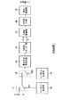
図1は、送信装置1の構成例を表している。送信信号は、スイッチ11に供給される。ユニークワード生成部12は、ユニークワードW1(詳細は、図13を参照して後述する)を生成し、スイッチ11に供給する。スイッチ11は、供給された送信する信号と、ユニークワード生成部12より供給されたユニークワードW1の出力を切り換え、その出力をスイッチ13に供給する。スイッチ13は、スイッチ11より供給された入力データまたはユニークワードW1と、ユニークワード生成部14により生成されたユニークワードW2(詳細は、図13を参照して後述する)の一方を選択し、畳み込み符号化部15へ出力する。
【0012】
畳み込み符号化部15は、スイッチ13より供給されるデータに対して、符号化率1/2の畳み込み符号化処理を施し、QASK(Quadrature Amplitude Shift Keying)マッピング部16に供給する。QASKマッピング部16は、畳み込み符号化部15より供給されたデータを、所定の信号にマッピング変調し、その同相成分I信号と直交成分Q信号を、QAM(Quadrature Amplitude Modulation)変調部17にそれぞれ出力する。QAM変調部17は、供給された同相成分I信号と直交成分Q信号をQAM変調し、ナイキストフィルタ18に供給する。ナイキストフィルタ18は、供給された信号をフィルタ処理し、直交変調部19に供給する。直交変調部19は、供給された信号を直交変調し、RF(Radio Frequency)信号を生成し、伝送路2に送信する。
【0013】
図2は、衛星回線などの伝送路2を模式的に表したものである。送信装置1から送信されたRF信号は、乗算部21に供給される。乗算部1は、供給された信号に周波数オフセットを乗算し、加算部22に出力する。加算部22は、供給された信号にノイズを加算し、受信装置3に送信する。
【0014】
図3は、受信装置3の構成例を表している。受信されたRF信号は、AGC(Automatic Gain Controller)31に供給される。AGC31は、供給された信号の振幅が一定になるように制御して、シンボルクロック生成回路32に出力する。シンボルクロック生成回路32(詳細は、図4を参照して後述する)は、シンボルポジション(シンボルクロック)を生成し、タイミング信号発生回路33に出力する。また、シンボルクロック生成回路32は、AGC31より供給された信号を、内部で生成したシンボルポジションに同期して補間し、補間信号を、C/Nメータ34およびキャリア再生回路36に出力する。
【0015】
タイミング信号発生回路33は、シンボルクロック生成回路32より供給されたシンボルポジションからゼロクロスタイミング信号およびピークタイミング信号を生成し、C/Nメータ34に出力する。
【0016】
C/Nメータ34(詳細は、図5乃至図7を参照して後述する)は、供給された信号から符号判定点と符号変化点を計測し、その電力比を表示回路35に出力する。表示回路35は、供給された信号を表示する。
【0017】
キャリア再生回路36(詳細は、図8および図9を参照して後述する)は、シンボルクロック生成回路32より供給された補間信号からキャリアを再生し、データ判定回路37に出力する。
【0018】
データ判定回路37は、キャリア再生回路36から供給された信号から、シンボル(データ)を判定し、判定したシンボルをユニークワード検出回路38に出力する。
【0019】
ユニークワード検出回路38(詳細は、図10を参照して後述する)は、予めユニークワードが設定されており、データ判定回路37より供給された信号との相関をとり、その相関値が所定の閾値以上となったとき、ユニークワードを検出したことを示す検出信号をフレーム同期検出回路39に出力する。
【0020】
フレーム同期検出回路39(詳細は、図14を参照して説明する)は、ユニークワード検出回路38より供給された信号からフレームの同期信号を検出し、その検出結果をマイクロコンピュータ(以下、マイコンと称する)40に出力する。
【0021】
マイコン40は、C/Nメータ34より供給された信号と、フレーム同期検出回路39より供給された検出結果から、フレームに同期しているか否かを判定し、キャリア再生回路36に掃引する周波数ステップ幅を変化させる信号を出力する。
【0022】
図4は、図3のシンボルクロック生成回路32の構成例を表している。インタポレータ51は、AGC31より供給された信号を、後述するタイミングコントローラ66より供給されたシンボルポジションに同期して補間し、補間信号をC/Nメータ34および誤差検出器52に出力する。
【0023】
誤差検出器52は、供給された信号の誤差を検出する。誤差検出器52の分離部53は、インタポレータ51より供給された信号を同相成分I信号と直交成分Q信号に分離し、同相成分I信号を加算部54および遅延部55に出力し、直交成分Q信号を加算部58および遅延部59に出力する。
【0024】
加算部54は、分離部53より供給された同相成分I信号と、遅延部55により1サンプル分だけ遅延された信号を加算し、平均値生成部56に出力する。平均値生成部56は、供給された信号の平均値を演算し、乗算部57に出力する。乗算部57は、供給された信号を2乗し、加算部62に出力する。
【0025】
一方、加算部58は、分離部53より供給された直交成分Q信号と、遅延部59により1サンプル分だけ遅延された信号を加算し、平均値生成部60に出力する。平均値生成部60は、供給された信号の平均値を演算し、乗算部61に出力する。乗算部61は、供給された信号を2乗し、加算部62に出力する。
【0026】
加算部62は、乗算部57より供給された信号と乗算部61より供給された信号を加算し、減算部63および遅延部64に出力する。減算部63は、加算部62より供給された信号と、遅延部64により1サンプル分だけ遅延された信号を減算する。すなわち、これにより、1サンプル前の値と現在の値との誤差が演算される。この誤差は、LPF(Low Pass Filter)65に出力される。
【0027】
LPF65は、供給された誤差信号の高域周波数成分をカットし、低域周波数成分のみを通過し、タイミングコントローラ66に出力する。タイミングコントローラ66は、供給された信号からシンボルポジションを生成し、インタポレータ51およびタイミング信号発生回路33に出力する。
【0028】
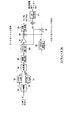
図5は、図3のC/Nメータ34の構成例を表している。シンボルクロック生成回路32のインタポレータ51から出力された補間信号は、分離器81に供給される。分離器81は、供給された信号を同相成分I信号と直交成分Q信号に分離し、同相成分I信号をナイキストフィルタ82に出力し、直交成分Q信号をナイキストフィルタ83に出力する。ナイキストフィルタ82は、供給された同相成分I信号をフィルタ処理し、合成器84に出力する。ナイキストフィルタ83は、供給された直交成分Q信号をフィルタ処理し、合成器84に出力する。合成器84は、供給された同相成分I信号と直交成分Q信号を複素信号として合成し、振幅抽出器85に出力する。振幅抽出器85は、供給された信号から振幅信号を抽出し、アイセンタ測定器86に出力するとともに、ゼロクロス点測定器90に出力する。
【0029】
アイセンタ測定器86は、タイミング信号発生回路33より供給されたピークタイミング信号のタイミングで、振幅抽出器85より供給された振幅信号のレベル(符号判定点(アイパターン観測において、アイの開いているところ)のレベル)を測定し、増幅器87に出力するとともに、減算器91に出力する。
【0030】
ゼロクロス点測定器90は、タイミング信号発生回路33より供給されたゼロクロスタイミング信号のタイミングを用いて、振幅抽出器85より供給された振幅信号のレベル(符号変化点(ゼロクロス点)のレベル)を測定し、減算器88に出力するとともに減算器91に出力する。
【0031】
増幅器87は、アイセンタ測定器86より供給された信号を増幅し、減算器88に出力する。減算器88は、ゼロクロス点測定器90より供給された符号変化点のレベルの信号から、増幅器87より供給された符号判定点のレベルの信号を減算し、逆数生成器89に出力する。逆数生成器89は、供給された信号の逆数を生成し、乗算器92に出力する。
【0032】
減算器91は、アイセンタ測定器86より供給された符号判定点のレベルの信号から、ゼロクロス点測定器90より供給された符号変化点のレベルの信号を減算し、乗算器92に出力する。
【0033】
乗算器92は、逆数生成器89より供給された信号と減算器91より供給された信号を乗算し、dB変換器93に出力する。dB変換器93は、供給された信号をデシベル単位の信号に変換し、表示回路35に出力するとともにマイコン40に出力する。
【0034】
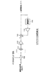
図6は、アイセンタ測定器86の構成例を表している。図5の振幅抽出器85より出力された信号は、スイッチ100を介して乗算部101に入力される。図3のタイミング信号発生回路33より供給されたピークタイミング信号は、スイッチ100をオンまたはオフさせる。乗算部101は、供給された信号を2乗し、増幅部102に出力する。増幅部102は、供給された信号を増幅し、加算部103に出力する。加算部103は、増幅部102より供給された信号と増幅部105より供給された信号を加算し、遅延部104に出力するとともに、図5の増幅器87に出力する。
【0035】
遅延部104は、供給された信号を所定の遅延量(1サイクル分)だけ遅延し、増幅部105に出力する。増幅部105は、供給された信号を増幅し、加算部103に出力する。すなわち、加算部103、遅延部104、および増幅部105により積分処理が行われる。
【0036】
図7は、ゼロクロス点測定器90の構成例を表している。図5の振幅抽出器85より出力された信号は、スイッチ110を介して乗算部111に入力される。図3のタイミング信号発生回路33より供給されたゼロクロスタイミング信号は、スイッチ110をオンまたはオフさせる。乗算部111は、供給された信号を2乗し、増幅部112に出力する。増幅部112は、供給された信号を増幅し、加算部113に出力する。加算部113は、増幅部112より供給された信号と増幅部115より供給された信号を加算し、遅延部114に出力するとともに、図5の減算器88および減算器91に出力する。
【0037】
遅延部114は、供給された信号を所定の遅延量(1サイクル分)だけ遅延し、増幅部115に出力する。増幅部115は、供給された信号を増幅し、加算部113に出力する。すなわち、加算部113、遅延部114、および増幅部115により積分処理が行われる。
【0038】
このように、アイセンタ測定器86とゼロクロス点測定器90は、サンプリングするタイミングが異なるだけで、その構成は同一とされている。
【0039】
図8は、図3のキャリア再生回路36の構成例を表している。図4のシンボルクロック生成回路32のインタポレータ51より供給された補間信号は、分離器121および遅延器125に入力される。分離器121は、供給された信号を同相成分I信号と直交成分Q信号に分離し、同相成分I信号をLPF122に出力し、直交成分Q信号をLPF123に出力する。LPF122は、供給された同相成分I信号の高域周波数成分を除去し、低域周波数成分をコスタスループ器124に出力する。LPF123は、供給された直交成分Q信号の高域周波数成分を除去し、低周波数成分をコスタスループ器124に出力する。
【0040】
コスタスループ器124(詳細は、図9を参照して後述する)は、供給された信号から逆相の位相誤差を含むキャリアを生成する。乗算器126は、コスタスループ器124より供給された逆相の位相誤差信号を含むキャリアと、遅延器125により所定の遅延時間(分離器121、LPF122、LPF123、およびコスタスループ器124の処理時間に対応する時間)だけ遅延された信号を乗算して、位相誤差成分が相殺されたキャリアを生成し、分離器127に出力する。分離器127は、供給された信号を同相成分I信号と直交成分Q信号に分離し、分離した同相成分I信号をナイキストフィルタ128に出力するとともに、直交成分Q信号をナイキストフィルタ129に出力する。ナイキストフィルタ128とナイキストフィルタ129は、供給された信号をフィルタ処理し、図3のデータ判定回路37に出力する。
【0041】
図9は、コスタスループ器124の構成例を表している。図8のLPF122およびLPF123より供給された同相成分I信号と直交成分Q信号は、合成部141に供給される。合成部141は、供給された同相成分I信号と直交成分Q信号を複素信号として合成し、乗算部142に出力する。乗算部142は、供給された信号を2乗し、乗算部143に出力する。
【0042】
乗算部143は、乗算部142より供給された信号と位相反転部159より供給された信号を乗算し、その位相誤差にあたる位相誤差信号を含むキャリアを位相抽出部144に出力する。位相抽出部144は、乗算部143より供給された複素信号から位相成分を抽出し、増幅部146に出力するとともに、増幅部147に出力する。
【0043】
増幅部146は、マイコン40より供給される制御信号により増幅率が制御される位相抽出部144より供給された位相信号を増幅し、加算部150に出力する。増幅部147も、マイコン40より供給される制御信号により増幅率が制御されるようになされており、位相抽出部144より供給された位相信号を増幅し、加算部148に出力する。加算部148は、増幅部147より供給された信号と遅延部149により所定の遅延量(1シンボル分)だけ遅延された信号を加算し(増幅部147の出力を積分し)、遅延部149と加算部150に出力する。なお、遅延部149は、マイコン40より供給される制御信号により初期位相が制御されるようになされている。
【0044】
加算部150は、増幅部146より供給された位相信号と、加算部148より供給された位相信号を加算し、加算部152に出力する。増幅部146、増幅部147、加算部148、遅延部149、および加算部150により、ラングリード型のループフィルタ145が構成されている。
【0045】
加算部152は、加算部150より供給された信号(ループフィルタ145より供給された信号)と、遅延部154により所定の遅延量(1シンボル分)だけ遅延された信号を加算し、モジュロ部153に出力する。モジュロ部153は、加算部152より供給された位相信号を0乃至2πの範囲の値に変換し、遅延部154と遅延部155に出力する。遅延部155は、供給された位相信号を1シンボル分だけ遅延した後、変換部156に出力する。変換部156は、供給された位相信号を複素信号に変換した後、位相反転部157と乗算部158に出力する。加算部152、モジュロ部153、遅延部154、遅延部155、および変換部156により、VCO(Voltage Controlled Oscillator)151が構成されている。
【0046】
位相反転部157は、供給された位相信号の位相を反転し、図8の乗算部126に出力するとともに、乗算部158に出力する。乗算部158は、変換部156より供給された位相信号を2乗し、位相反転部159に出力する。位相反転部159は、供給された位相信号の位相を反転し、乗算部143に出力する。
【0047】
図10は、図3のユニークワード検出回路38の構成例を表している。データ判定回路37より供給された信号は、QASKデマッピング器171に供給される。QASKデマッピング器171は、供給された信号をデマッピング処理し、ユニークワード検出器172に供給するするとともに、遅延器173に供給する。
【0048】
ユニークワード検出器172は、予め、ユニークワードW2が設定されており、この値と、QASKデマッピング器171より供給された信号との相関を演算し、その相関値を相関値合成器175に出力する。
【0049】
一方、遅延器173は、供給された信号を所定の遅延量(ユニークワードW1とユニークワードW2の距離に対応する時間)だけ遅延し、ユニークワード検出器174に供給する。
【0050】
ユニークワード検出器174は、予め、ユニークワードW1が設定されており、この値と、遅延器173より供給された信号との相関を演算し、その相関値を相関値合成器175に出力する。
【0051】
相関値合成器175は、ユニークワード検出器172とユニークワード検出器174からの相関値を合成(加算)し、その値が所定の閾値以上となったとき、ユニークワードを検出したことを示す検出信号を図3のフレーム同期検出回路39に出力する。すなわち、ユニークワード検出器172とユニークワード検出器174で、それぞれユニークワードW2とユニークワードW1が検出されたとき、検出信号が相関値合成器175に出力される。なお、相関値合成器175は、検出信号を出力したとき、リセットされるようになされている。
【0052】
次に、送信装置1、伝送路2、および受信装置3の動作について説明する。まず、送信装置1の動作について説明する。送信する信号は、スイッチ11に供給される。ユニークワード生成部12はユニークワードW1を生成し、スイッチ11に供給する。スイッチ11は、まず、ユニークワード生成部12より供給されるユニークワードW1を選択し、ユニークワードW1をスイッチ13に出力する。スイッチ13は、供給されたユニークワードW1を選択し、畳み込み符号化部15に供給する。次に、スイッチ11は、入力されたTMCC信号を選択し、スイッチ13を介して畳み込み符号化部15に出力する。さらに、スイッチ13は、ユニークワード生成部14で生成されたユニークワードW2を選択し、畳み込み符号化部15に出力する。
【0053】
畳み込み符号化部15は、供給されたユニークワードW1、TMCC、およびユニークワードW2に、符号率1/2の畳み込み符号化処理を施し、QASKマッピング部16に供給する。QASKマッピング部16は、畳み込み符号部15より供給されたデータを、所定の信号にマッピング変調し、その同相成分I信号と直交成分Q信号をQAM変調部17にそれぞれ出力する。QAM変調部17は、供給された同相成分I信号と直交成分Q信号をQAM変調し、ナイキストフィルタ18に供給する。ナイキストフィルタ18は、供給された信号をフィルタ処理し、直交変調部19に供給する。直交変調部19は、供給された信号を直交変調し、RF信号を生成して伝送路2に出力する。
【0054】
図2の伝送路2の乗算部21は、供給された信号に周波数オフセットを乗算し、加算部22に出力する。加算部22は、供給された信号にノイズを加算し、受信装置3に送信する。
【0055】
次に、受信装置3の動作について図11のフローチャートを用いて説明する。受信された信号は、AGC31に供給される。AGC31は、供給された信号の振幅を一定にし、シンボルクロック生成回路32に出力する。
【0056】
ステップS1において、シンボルクロック生成回路32は、AGC31より供給された信号のシンボルの位相に同期させ、シンボルクロックを生成する。すなわち、AGC31よりシンボルクロック生成回路32に供給された信号は、図4のインタポレータ51に供給される。インタポレータ51は、AGC31より供給される信号とタイミングコントローラ66より供給されるシンボルポジションに同期して補間し、補間信号を生成し、C/Nメータ34に出力するとともに、誤差検出器52の分離部53に出力する。
【0057】
分離部53は、インタポレータ51より供給された信号を、同相成分I信号と直交成分Q信号に分離し、同相成分I信号を加算部54および遅延部55に出力し、直交成分Q信号を加算部58および遅延部59に出力する。
【0058】
加算部54は、分離部53より供給された同相成分I信号と遅延部55により所定の1シンボル分だけ遅延された信号を加算し、平均値生成部56に出力する。平均値生成部56は、供給された信号の平均値を生成し、乗算部57に出力する。乗算部57は、供給された信号を2乗し、加算部62に出力する。
【0059】
加算部58は、分離部53より供給された直交成分Q信号と遅延部59により1シンボル分だけ遅延された信号を加算し、平均値生成部60に出力する。平均値生成部60は、供給された信号の平均値を生成し、乗算部61に出力する。乗算部61は、供給された信号を2乗し、加算部62に出力する。
【0060】
加算部62は、乗算部57および乗算部61より供給された信号を加算し、減算部63に出力するとともに、遅延部64に出力する。減算部63は、加算部62より供給された信号から、遅延部64により1シンボル分だけ遅延された信号を減算し、その誤差信号をLPF65に出力する。この誤差信号は、誤差検出器52に供給された補間信号のシンボル位置のずれに対応した誤差信号となっている。
【0061】
LPF65は、供給された信号の高域周波数成分を除去し、低域周波数成分を通過し、タイミングコントローラ66に出力する。タイミングコントローラ66は、供給された信号からシンボルポジションを生成し、タイミング信号発生回路33に出力するとともに、インタポレータ51に出力する。
【0062】
タイミング信号発生回路33は、供給されたシンボルポジションに基づいて、ピークタイミング信号およびゼロクロスタイミング信号を生成し、ピークタイミング信号を図5のC/Nメータ34のアイセンタ測定器86に出力するとともに、ゼロクロスタイミング信号を図5のC/Nメータ34のゼロクロス点測定器90に出力する。
【0063】
ステップS2において、C/Nメータ34は、タイミング信号発生回路33より供給されたゼロクロスタイミング信号、ピークタイミング信号、およびシンボルクロック生成回路32より供給された補間信号からC/N比を計測する。すなわち、シンボルクロック生成回路32より供給された補間信号は、C/Nメータ34の分離器81に供給される。分離器81は、供給された信号を同相成分I信号と直交成分Q信号に分離し、同相成分I信号をナイキストフィルタ82に出力し、直交成分Q信号をナイキストフィルタ83に出力する。ナイキストフィルタ82は、供給された同相成分I信号をフィルタ処理し、合成器84に出力する。ナイキストフィルタ83は、供給された直交成分Q信号をフィルタ処理し、合成器84に出力する。合成器84は、供給された同相成分I信号と直交成分Q信号を複素信号として合成し、振幅抽出器85に出力する。振幅抽出器85は、供給された信号から振幅を抽出し、アイセンタ測定器86に出力するとともに、ゼロクロス点測定器90に出力する。
【0064】
アイセンタ測定器86に供給された、振幅抽出器85からの振幅信号は、スイッチ100を介して乗算部101に供給される。スイッチ101は、図3のタイミング信号発生回路33からのピークタイミング信号に基づいてオンされる。従って、乗算部101には、振幅抽出器85より供給された振幅信号が、タイミング信号発生回路33より供給されたピークタイミング信号のタイミングで供給される。乗算部101は、供給された信号を2乗し、増幅部102に出力する。増幅部102は、供給された信号を増幅し、加算部103に出力する。加算部103は、増幅部102より供給された信号と増幅部105より供給された信号を加算し、遅延部104に出力するとともに、図5の増幅器87に出力する。加算部103から出力された信号は、符号判定点のレベルを示す信号となっている。なお、増幅部105より供給された信号は、遅延部104により所定の遅延量(1サンプル分)だけ遅延され、増幅部105により増幅されたものである。
【0065】
一方、ゼロクロス点測定器90に供給された、振幅抽出器85からの振幅信号は、スイッチ110を介して乗算部111に供給される。スイッチ110は、図3のタイミング信号発生回路33からのゼロクロスタイミング信号に基づいてオンされる。従って、乗算部111には、振幅抽出器85より供給された振幅信号が、タイミング信号発生回路33より供給されたゼロクロスタイミング信号のタイミングで供給される。乗算部111は、供給された信号を2乗し、増幅部112に出力する。増幅部112は、供給された信号を増幅し、加算部113に出力する。加算部113は、増幅部112より供給された信号と増幅部115より供給された信号を加算し、遅延部114に出力するとともに、図5の減算器88と減算器91に出力する。加算部113から出力された信号は、符号変化点のレベルを示す信号となっている。なお、増幅部115より供給された信号は、遅延部114により所定の遅延量(1サンプル分)だけ遅延され、増幅部115により増幅されたものである。
【0066】
ここで、例えば、ノイズがない場合の符号判定点の電力をC=bs0とし、符号変化点の電力をaC=bi0とする。なお、aは、十分長いエネルギー拡散された信号の場合、変調方式に依存するが一定値となる。このような場合、ノイズが加わったときの符号判定点の電力は、C+N=b sとなり、符号変化点の電力は、aC+N=b iとなる。アイセンタ測定器86からは、符号変化点の電力信号bsが出力され、ゼロクロス点測定器90からは、符号変化点の電力信号biが出力されることになる。なお、aとしては、例えば数値0.8375が用いられる。
【0067】
図6のアイセンタ測定器86の加算部103より出力された符号判定点電力信号bsは、図5の増幅器87に供給される。増幅器87は、供給された信号を0.8375倍(=a)に増幅し、電力信号0.8375×bsを加算部88に出力する。
【0068】
また、図7のゼロクロス点測定器90の加算部113より出力された信号は、図5の減算器91に供給されるとともに、減算器88に供給される。減算器91は、供給された符号判定点電力信号bsから符号変化点電力信号biを減算し、電力信号(bs-bi)を乗算器92に出力する。
【0069】
減算器88は、ゼロクロス点測定器90より供給された符号変化点電力信号biから、増幅器87より供給された符号判定点電力信号0.8375×bsを減算し、電力信号(bi-0.8375×bs)を生成して、逆数生成器89に出力する。
【0070】
逆数生成器89は、供給された電力信号(bi-0.8375×bs)の逆数を生成し、電力信号1/(bi-0.8375×bs)を乗算器92に出力する。
【0071】
乗算器92は、逆数生成器89より供給された電力信号1/(bi-0.8375×bs)と減算器91より供給された電力信号(bs-bi)を乗算し、電力信号(bs-bi)/(bi-0.8375×bs)を生成し、dB変換器93に出力する。dB変換器93は、供給された信号をデシベル単位の信号に変換し、表示回路35に出力するとともに、マイコン40に出力する。
【0072】
表示回路35は、供給された信号を表示する。図16を参照して後述するが、C/Nメータ34からの出力とC/N比とは1対1に対応しており、C/Nメータ34からの出力によりC/N比が推定できる。
【0073】
ステップS3において、マイコン40は、C/Nメータ34より供給された信号を予め設定している閾値と比較し、閾値との差が予め設定している基準値以上であるか否かを判定し、基準値以下である場合、ステップS4に進み、マイコン40は、キャリア再生回路36を制御し、周波数を掃引してキャリア同期を実行させる。
【0074】
すなわち、シンボルクロック再生回路32のインタポレータ51から出力された補間信号は、図8のキャリア再生回路36の分離器121および遅延器125に供給される。分離器121は、供給された信号を同相成分I信号と直交成分Q信号に分離し、同相成分I信号をLPF122に出力し、直交成分Q信号をLPF123に出力する。LPF122は、供給された同相成分I信号の高域周波数成分を除去し、低域周波数成分をコスタスループ器124に出力する。LPF123は、供給された直交成分Q信号の高域周波数成分を除去し、低域周波数成分をコスタスループ器124に出力する。
【0075】
遅延器125は、供給された信号を所定の遅延時間(分離器121、LPF122、LPF123、およびコスタスループ器124の処理時間に対応する時間)だけ遅延し、乗算器126に出力する。
【0076】
LPF122およびLPF123より供給された同相成分I信号と直交成分Q信号は、図9のコスタスループ器124の合成部141に供給される。合成部141は、供給された同相成分I信号と直交成分Q信号を複素信号として合成し、乗算部142に出力する。乗算部142は、供給された信号を2乗し、乗算部143に出力する。
【0077】
乗算部143は、乗算部142より供給された信号と位相反転部159より供給された信号を乗算し、その位相誤差にあたる位相誤差信号を位相抽出部144に出力する。位相抽出部144は、乗算部143より供給された複素信号から位相信号を抽出し、増幅部146に出力するとともに、増幅部147に出力する。
【0078】
増幅部146は、位相抽出部144より供給された位相信号を、マイコン40より供給された増幅率に基づいて増幅し、加算部150に出力する。増幅部147も、位相抽出部144より供給された位相信号を、マイコン40より供給された増幅率に基づいて増幅し、加算部148に出力する。加算部148は、増幅部147より供給された信号と遅延部149により所定の遅延量(1シンボル分)だけ遅延された信号を加算し、遅延部149と加算部150に出力する。加算部150は、増幅部146より供給された位相信号と、加算部148より供給された位相信号を加算し、加算部152に出力する。
【0079】
加算部152は、加算部150より供給された信号と、遅延部154により所定の遅延量(1シンボル分)だけ遅延された信号を加算し、モジュロ部153に出力する。モジュロ部153は、加算部152より供給された位相信号を0乃至2πの範囲の値に変換し、遅延部154と遅延部155に出力する。遅延部155は、供給された位相信号を1シンボル分だけ遅延した後、変換部156に出力する。変換部156は、供給された位相信号を複素信号に変換した後、位相反転部157と乗算部158に出力する。位相反転部157は、供給された位相信号の位相を反転し、図8の乗算部126に出力するとともに乗算部158に出力する。なお、位相反転部159より乗算部143に供給される信号は、変換部156より供給された信号が、乗算部158で2乗され、位相反転部159で位相が反転されたものである。
【0080】
図8の乗算器126は、コスタスループ器124より供給されたキャリアの周波数誤差信号と遅延器125により所定の時間だけ遅延された信号を乗算し、分離器127に出力する。分離器127に出力された信号は、位相の誤差が除去されたキャリアとなっている。分離器127は、供給された信号を同相成分I信号と直交成分Q信号に分離し、同相成分I信号をナイキストフィルタ128に出力するとともに、直交成分Q信号をナイキストフィルタ129に出力する。ナイキストフィルタ128とナイキストフィルタ129は、供給された信号をフィルタ処理し、図3のデータ判定回路37に出力する。
【0081】
データ判定回路37の動作について、図12を用いて説明する。図12は、BPSK変調方式シンボルマッピングを表している。データ判定回路37には、予め、同相成分Iと直交成分Qの組(I,Q)に対する閾値が設けられている。例えば、同相成分I信号に対して閾値180(直線180が示す閾値)が設定されている。データ判定回路37は、供給された同相成分I信号が、例えば、予め設定されている閾値180よりも大きい場合(すなわち、同相成分Iが0より大きい場合)、シンボル[0]を検出したと判定し、検出したシンボルを復調し、図10のユニークワード検出回路38に出力する。また、図8のキャリア再生回路36のナイキストフィルタ129より供給された同相成分Q信号が、例えば、予め設定している閾値180よりも小さい場合(すなわち、同相成分Qが0より小さい場合)、シンボル[1]を検出したと判定し、検出したシンボルを復調し、図10のユニークワード検出回路38に出力する。
【0082】
図3のデータ判定回路37から出力された信号は、図10のユニークワード検出回路38のQASKデマッピング器171に供給される。QASKデマッピング器171は、供給された信号をデマッピング処理し、ユニークワード検出器172に供給するとともに、遅延器173に供給する。
【0083】
ユニークワード検出器172は、予め、ユニークワードW2が設定されており、この値と、QASKデマッピング器171より供給された信号との相関を演算し、その相関値を相関値合成器175に出力する。
【0084】
一方、遅延器173は、供給された信号を所定の遅延量(ユニークワードW1とユニークワードW2の距離に対応する分)だけ遅延し、ユニークワード検出器175に出力する。
【0085】
ユニークワード検出器173は、予め、ユニークワードW1が設定されており、この値と、QASKデマッピング器171より供給された信号との相関を演算し、その相関値を相関値合成器175に出力する。
【0086】
相関値合成器175は、ユニークワード検出器172とユニークワード検出器174からの相関値を合成(加算)し、その値が所定の閾値以上となったとき、ユニークワードを検出したことを示す検出信号を図3のフレーム同期検出回路39に出力する。すなわち、ユニークワード検出器172とユニークワード検出器174でそれぞれユニークワードW2とユニークワードW1が検出されたとき、検出信号が相関値合成器175に出力される。
【0087】
ここで、ユニークワード検出器172およびユニークワード検出器174の動作を図13を用いて詳細に説明する。まず、ユニークワード検出器172に供給される信号について説明する。この信号は、図13(A)に示すように、1フレームが96ビットで構成され、最初の16ビット(TAB1)または最後の16ビット(TAB2)の位置に、図13(B)に示すように、それぞれユニークワードW1またはユニークワードW2が配置される。具体的には、8つのフレームにより構成されるスーパーフレームのうち、フレームの先頭のTAB1には、ユニークワードW1が配置され、後部のTAB2には、ユニークワードW2が配置される。但し、残りの7フレームにおいては、TAB1にユニークワードW1が配置されるが、TAB2には、ユニークワードW3が配置される。なお、この例においては、ユニークワードw1として値(1B95)が設定され、ユニークワードW2として値(A340)が設定され、ユニークワードW3として値(5CBF)が設定されている(いずれも16進表記)。64ビットのデータとしては、変調方式や符号化率等の伝送情報を含むTMCCが配置されている。
【0088】
図13(C)は、符号化率1/2の畳み込み符号処理が施されている信号を表している。但し、先頭の4ビットは、前段の信号の最後の4ビットである。この4ビットを除く信号は、畳み込み符号化されているため、合計192ビットの信号とされている。このうちのユニークワードW1とユニークワードW2にあたる部分(32ビット)のそれぞれの先頭の12ビットは、畳み込み符号化の際に前段のビットと併せて符号化されているため、ユニークワードとして用いることができない。したがって、ユニークワードとしては、残りの20ビットが用いられており、ユニークワードW1の先頭のビットと、ユニークワードW2の先頭のビットとは、160ビット分離れている(このビット数に対応する遅延が、図10の遅延器173により与えられる)。
【0089】
次に、例えば、図13(C)に示した信号が供給されているものとして、ユニークワード検出器172およびユニークワード検出器174の動作について説明する。ユニークワード検出器172には、20ビットのユニークワードW2が予め設定されている。そして、ユニークワード検出器174は、供給される信号との相関を1ビットづつ演算し、一致したとき1、一致しなかったとき−1を、相関値合成器175に出力する。例えば、演算した相関値が18の場合、相関値18が相関値合成器175に出力される。
【0090】
一方、ユニークワード検出器174に供給される信号は、ユニークワード検出器172に供給される信号よりもユニークワードW2とユニークワードW1の距離(具体的には160ビット)に対応する分だけ遅延され供給されている。これにより、ユニークワード検出器172にユニークワードW2が入力されるタイミングにおいて、ユニークワード検出器174に、ユニークワードW1が入力されることになる。そして、ユニークワード検出器174は、供給される信号との相関を1ビットづつ演算し、一致したとき1、一致しなかったとき−1を相関値合成器175に出力する。例えば、演算した相関値が18の場合、相関値18が相関値合成器175に出力される。
【0091】
相関値合成器175は、ユニークワード検出器172とユニークワード検出器174からの相関値を合成(加算)し、その値が所定の閾値以上となったとき、ユニークワードを検出したことを示す検出信号を図3のフレーム同期検出回路39に出力する。すなわち、ユニークワード検出器172とユニークワード検出器174でそれぞれユニークワードW2とユニークワードW1が検出されたとき、検出信号が相関値合成器175に出力される。これにより、BPSK変調、QPSK変調信号または8PSK変調信号を復調するための時間基準(同期信号)が得られたことになる。
【0092】
図11に戻って、ステップS5において、フレーム同期検出回路39は、供給された信号からフレームが同期しているか否かを検出し、その検出結果をマイコン40に出力する。このフレーム同期検出回路39の処理の詳細は、図14のフローチャートに表されている。すなわち、図14のステップS21において、フレーム同期検出回路39は、ユニークワード検出回路38より検出信号が入力されたか否かを判定する。ステップS21において、検出信号が入力されたと判定された場合、ステップS22に進む。
【0093】
ステップS22において、フレーム同期検出回路39は、ユニークワード検出回路38より検出信号が3回連続して入力されたか否かを判定する。検出信号が3回連続して入力された場合、ステップS23において、フレーム同期検出信号をマイコン40に出力してステップS24に移る。検出信号が3回連続して入力されなかった場合、ステップS24の処理はスキップされ、ステップS25に移る。このように、検出信号が3回連続して入力されたか否かを判定することにより、検出信号の入力の有無を判定するのは、誤検出率を減少する事と誤って同期はずれするのを保護するためである。
【0094】
図11に戻って、ステップS5において、マイコン40は、フレーム同期検出回路39より供給された検出結果より、フレーム同期しているか否かを判定し、フレーム同期していると判定した場合、処理を終了し、フレーム同期していないと判定した場合、ステップS6において、キャリア再生回路36に、周波数のステップ幅を変化させる信号を出力する(図9のコスタスループ器124の初期値を変更する)。この処理は、ステップS5で、フレーム同期したと判定されるまで繰り返される。
【0095】
ステップS5において、フレーム同期していると判定された場合、キャリア再生回路36は、マイコン40より供給された周波数のステップ幅でキャリアを再生し、データ判定回路37に出力する(キャリア再生回路36の詳細な処理は、上述した場合と同様であるので省略する)。
【0096】
一方、ステップS3において、マイコン40は、C/Nメータ34より供給された信号と予め設定している閾値との差が、予め設定している基準値以上であると判定した場合、ステップS7において、マイコン40は、キャリア再生回路36に、掃引する周波数の誤差0およびループの雑音帯域幅を初期値に戻す信号を出力する(図9の増幅部146と増幅部147の増幅率を所定の値に設定し、遅延部149に所定の初期値を設定する)。キャリア再生回路36は、供給された初期値の周波数の誤差および雑音帯域幅でキャリアを再生し、データ判定回路37に出力する(キャリア再生回路36の詳細な処理は、上述した場合と同様であるので省略する)。
【0097】
データ判定回路37は、キャリア再生回路36より供給された信号を、予め設定している閾値に基づいて、シンボルを検出できたか否かを判定し、シンボルを検出できたと判定した場合、検出したシンボルを復調し、ユニークワード検出回路38に出力する(データ判定回路37の詳細な処理は、上述した場合と同様であるので省略する)。
【0098】
ユニークワード検出回路38は、供給された信号からユニークワードを検出し、相関値を合成して、その値が所定の閾値以上となったとき、ユニークワードを検出したことを示す検出信号をフレーム同期検出回路39に出力する(ユニークワード検出回路38の詳細な処理は、上述した場合と同様であるので省略する)。
【0099】
フレーム同期検出回路39は、供給された信号からフレームが同期しているか否かを検出し、その検出結果をマイコン40に出力する(フレーム同期検出回路39の詳細な処理は、上述した場合と同様であるので省略する)。
【0100】
ステップS8において、マイコン40は、供給された検出結果から、フレームに同期しているか否かを判定し、フレームに同期していると判定されるまで、ステップS8に待機し、フレームに同期していると判定された場合、処理を終了する。
【0101】
以上のように、図3の受信装置3によれば、シンボル同期を捕った後に、符号判定点と符号変化点のレベル差を検出するようにしたので、C/N比を推定することができる。
【0103】
図15は、横軸にC/N比をとり、縦軸にC/Nメータ34の出力をとって表したものであり、変調方式をBPSK変調、8PSK変調が混在(ただしデータがすべて8PSK変調されている)したときの特性が示されている。上述したように、C/N比とC/Nメータ34からの出力の関係は、変調方式により曲線が上下するが、1対1に対応している。これより、C/Nメータ34からの出力によりC/N比が推定できることがわかる。
【0104】
なお、本明細書中において、システムの用語は、複数の装置、手段などにより構成される全体的な装置を意味するものとする。
【0105】
また、本明細書中において、上記処理を実行するコンピュータプログラムをユーザに提供する提供媒体には、磁気ディスク、CD−ROMなどの情報記録媒体の他、インターネット、ディジタル衛星などのネットワークによる伝送媒体も含まれる。
【0106】
【発明の効果】
以上のように、請求項1に記載の情報処理装置、請求項2に記載の情報処理方法、および請求項3に記載の提供媒体によれば、受信信号から符号判定点と符号変化点を検出するようにしたので、信号の雑音を推定することができる。
【図面の簡単な説明】
【図1】 送信装置1の構成例を示すブロック図である。
【図2】 伝送路2の構成例を示すブロック図である。
【図3】 本発明を適用した受信装置3の構成例を示すブロック図である。
【図4】 図3のシンボルクロック生成回路32の構成例を示すブロック図である。
【図5】 図3のC/Nメータ34の構成例を示すブロック図である。
【図6】 図5のアイセンタ測定器86の構成例を示すブロック図である。
【図7】 図5のゼロクロス点測定器90の構成例を示すブロック図である。
【図8】 図3のキャリア再生回路36の構成例を示すブロック図である。
【図9】 図8のコスタスループ器124の構成例を示すブロック図である。
【図10】 図3のユニークワード検出回路38の構成例を示すブロック図である。
【図11】 図3の受信装置3の動作を説明するフローチャートである。
【図12】 図3のデータ判定回路37の動作を説明する図である。
【図13】 図3のユニークワード検出回路38の動作を説明する図である。
【図14】 図3のフレーム同期検出回路39の動作を説明するフローチャートである。
【図15】 C/N メータ34の出力特性を示す図である。
[0001]
BACKGROUND OF THE INVENTION
The present invention relates to an information processing apparatus and method, and a providing medium, and in particular, by detecting a level difference between a sign determination point (where an eye is open in eye pattern observation) and a sign change point (zero cross point). The present invention relates to an information processing apparatus and method capable of detecting a / N (Carrier to Noise) ratio at high speed, and a providing medium.
[0002]
[Prior art]
Conventionally, when receiving radio waves from satellite broadcasting and detecting the C / N ratio from the received signal, it detects errors that occur when demodulating, or vector errors from the ideal symbol constellation, that is, deviation from the ideal symbol point. Like to do.
[0003]
[Problems to be solved by the invention]
However, in order to measure the C / N ratio by detecting errors that occur during demodulation or vector errors from the ideal symbol constellation, that is, deviation from the ideal symbol point, the received signal Need to be demodulated once. Therefore, since it is necessary to completely capture the carrier frequency synchronization, it takes time to detect the C / N ratio, and there is a problem that high-speed C / N ratio detection is difficult.
[0004]
The present invention has been made in view of such circumstances, and makes it possible to detect the C / N ratio at high speed.
[0005]
[Means for Solving the Problems]
  The information processing apparatus according to claim 1 includes: an amplitude value detection unit that detects an amplitude value from a received signal; and a code determination point detection unit that detects a code determination point based on the amplitude value detected by the amplitude value detection unit. And a sign change point detecting means for detecting a sign change point based on the amplitude value detected by the amplitude value detecting means,The first power signal obtained by subtracting the second received power at the code change point detected by the code change point detection means from the first received power at the code decision point detected by the code decision point detection means And a ratio of the second received power obtained by subtracting the first received power multiplied by a predetermined constant from the second received power,Noise detection means for detecting the relationship between the signal magnitude and the noise magnitude is provided.
[0006]
  An information processing method according to claim 2 includes an amplitude value detection step for detecting an amplitude value from a received signal, and a code determination point detection step for detecting a code determination point based on the amplitude value detected in the amplitude value detection step. A sign change point detecting step for detecting a sign change point based on the amplitude value detected in the amplitude value detecting step;A first power signal obtained by subtracting the second received power at the code change point detected at the code change point detection step from the first received power at the code decision point detected at the code decision point detection step And a ratio of the second received power obtained by subtracting the first received power multiplied by a predetermined constant from the second received power,And a noise detection step of detecting a relationship between the magnitude of the signal and the magnitude of the noise.
[0007]
  The providing medium according to claim 3 includes an amplitude value detection step for detecting an amplitude value from the received signal, a code determination point detection step for detecting a code determination point based on the amplitude value detected in the amplitude value detection step, and A sign change point detecting step for detecting a sign change point based on the amplitude value detected in the amplitude value detecting step;A first power signal obtained by subtracting the second received power at the code change point detected at the code change point detection step from the first received power at the code decision point detected at the code decision point detection step And a ratio of the second received power obtained by subtracting the first received power multiplied by a predetermined constant from the second received power,A computer-readable program for causing an information processing apparatus to execute a process including a noise detection step for detecting a relationship between a signal magnitude and a noise magnitude is provided.
[0008]
  In the information processing apparatus according to claim 1, the information processing method according to claim 2, and the providing medium according to claim 3, an amplitude value is detected from a received signal, and based on the detected amplitude value, A code determination point is detected, a code change point is detected based on the detected amplitude value, and a detected code determination pointReceived power atAnd sign change pointReceived power atFrom the signalSize andnoiseRelationship with sizeIs detected.
[0009]
DETAILED DESCRIPTION OF THE INVENTION
Embodiments of the present invention will be described below, but in order to clarify the correspondence between each means of the invention described in the claims and the following embodiments, in parentheses after each means, The features of the present invention will be described with the corresponding embodiment (however, an example) added. However, of course, this description does not mean that each means is limited to the description.
[0010]
  The information processing apparatus according to claim 1 is based on an amplitude value detection unit (for example, an amplitude extractor 85 in FIG. 5) that detects an amplitude value from a received signal, and an amplitude value detected by the amplitude value detection unit. A code determination point detection unit (for example, an eye center measuring device 86 in FIG. 5) for detecting a code determination point, and a code change point detection unit (for detecting a code change point based on the amplitude value detected by the amplitude value detection unit) For example, the zero cross point measuring device 90) in FIG. 5 and the code determination point detected by the code determination point detection means.From the first received power, At the sign change point detected by the sign change point detection meansA first power signal obtained by subtracting the second received power, and a second power signal obtained by subtracting the first received power multiplied by a predetermined constant from the second received power; From the ratio ofIt is characterized by comprising noise detecting means (for example, a multiplier 92 in FIG. 5) for detecting the relationship between the signal magnitude and the noise magnitude.
[0011]
FIG. 1 illustrates a configuration example of the transmission device 1. The transmission signal is supplied to the switch 11. The unique word generation unit 12 generates a unique word W1 (details will be described later with reference to FIG. 13) and supplies the generated word to the switch 11. The switch 11 switches between the supplied signal to be transmitted and the output of the unique word W1 supplied from the unique word generator 12, and supplies the output to the switch 13. The switch 13 selects one of the input data or the unique word W1 supplied from the switch 11 and the unique word W2 generated by the unique word generation unit 14 (details will be described later with reference to FIG. 13), and convolves it. The data is output to the encoding unit 15.
[0012]
The convolutional coding unit 15 performs convolutional coding processing with a coding rate of 1/2 on the data supplied from the switch 13 and supplies the data to a QASK (Quadrature Amplitude Shift Keying) mapping unit 16. The QASK mapping unit 16 performs mapping modulation on the data supplied from the convolutional coding unit 15 to a predetermined signal, and outputs the in-phase component I signal and the quadrature component Q signal to a QAM (Quadrature Amplitude Modulation) modulation unit 17, respectively. To do. The QAM modulator 17 performs QAM modulation on the supplied in-phase component I signal and quadrature component Q signal, and supplies them to the Nyquist filter 18. The Nyquist filter 18 performs a filtering process on the supplied signal and supplies it to the quadrature modulation unit 19. The quadrature modulation unit 19 performs quadrature modulation on the supplied signal, generates an RF (Radio Frequency) signal, and transmits it to the transmission path 2.
[0013]
FIG. 2 schematically shows a transmission path 2 such as a satellite line. The RF signal transmitted from the transmission device 1 is supplied to the multiplication unit 21. The multiplier 1 multiplies the supplied signal by the frequency offset and outputs the result to the adder 22. The adder 22 adds noise to the supplied signal, and transmits it to the receiving device 3.
[0014]
FIG. 3 illustrates a configuration example of the receiving device 3. The received RF signal is supplied to an AGC (Automatic Gain Controller) 31. The AGC 31 controls the supplied signal to have a constant amplitude, and outputs the signal to the symbol clock generation circuit 32. A symbol clock generation circuit 32 (details will be described later with reference to FIG. 4) generates a symbol position (symbol clock) and outputs it to the timing signal generation circuit 33. Further, the symbol clock generation circuit 32 interpolates the signal supplied from the AGC 31 in synchronization with the internally generated symbol position, and outputs the interpolation signal to the C / N meter 34 and the carrier recovery circuit 36.
[0015]
The timing signal generation circuit 33 generates a zero cross timing signal and a peak timing signal from the symbol positions supplied from the symbol clock generation circuit 32 and outputs them to the C / N meter 34.
[0016]
A C / N meter 34 (details will be described later with reference to FIGS. 5 to 7) measures a sign determination point and a sign change point from the supplied signal and outputs the power ratio to the display circuit 35. The display circuit 35 displays the supplied signal.
[0017]
The carrier recovery circuit 36 (details will be described later with reference to FIGS. 8 and 9) recovers the carrier from the interpolation signal supplied from the symbol clock generation circuit 32 and outputs the carrier to the data determination circuit 37.
[0018]
The data determination circuit 37 determines a symbol (data) from the signal supplied from the carrier reproduction circuit 36 and outputs the determined symbol to the unique word detection circuit 38.
[0019]
A unique word detection circuit 38 (details will be described later with reference to FIG. 10) has a unique word set in advance, takes a correlation with the signal supplied from the data determination circuit 37, and the correlation value is a predetermined value. When the threshold value is exceeded, a detection signal indicating that a unique word has been detected is output to the frame synchronization detection circuit 39.
[0020]
A frame synchronization detection circuit 39 (details will be described with reference to FIG. 14) detects a frame synchronization signal from the signal supplied from the unique word detection circuit 38, and the detection result is detected by a microcomputer (hereinafter referred to as a microcomputer). Output to 40).
[0021]
The microcomputer 40 determines whether it is synchronized with the frame from the signal supplied from the C / N meter 34 and the detection result supplied from the frame synchronization detection circuit 39, and sweeps it to the carrier reproduction circuit 36. Outputs a signal that changes the width.
[0022]
FIG. 4 shows a configuration example of the symbol clock generation circuit 32 of FIG. The interpolator 51 interpolates the signal supplied from the AGC 31 in synchronization with a symbol position supplied from the timing controller 66 described later, and outputs the interpolation signal to the C / N meter 34 and the error detector 52.
[0023]
The error detector 52 detects an error of the supplied signal. The separation unit 53 of the error detector 52 separates the signal supplied from the interpolator 51 into an in-phase component I signal and a quadrature component Q signal, and outputs the in-phase component I signal to the addition unit 54 and the delay unit 55. The signal is output to adder 58 and delay unit 59.
[0024]
The adder 54 adds the in-phase component I signal supplied from the separator 53 and the signal delayed by one sample by the delay unit 55 and outputs the result to the average value generator 56. The average value generation unit 56 calculates the average value of the supplied signal and outputs it to the multiplication unit 57. The multiplier 57 squares the supplied signal and outputs it to the adder 62.
[0025]
On the other hand, the addition unit 58 adds the orthogonal component Q signal supplied from the separation unit 53 and the signal delayed by one sample by the delay unit 59 and outputs the result to the average value generation unit 60. The average value generation unit 60 calculates the average value of the supplied signals and outputs it to the multiplication unit 61. The multiplier 61 squares the supplied signal and outputs the square to the adder 62.
[0026]
The adder 62 adds the signal supplied from the multiplier 57 and the signal supplied from the multiplier 61 and outputs the result to the subtractor 63 and the delay unit 64. The subtracting unit 63 subtracts the signal supplied from the adding unit 62 and the signal delayed by one sample by the delay unit 64. That is, an error between the value one sample before and the current value is calculated. This error is output to an LPF (Low Pass Filter) 65.
[0027]
The LPF 65 cuts the high frequency component of the supplied error signal, passes only the low frequency component, and outputs it to the timing controller 66. The timing controller 66 generates a symbol position from the supplied signal and outputs it to the interpolator 51 and the timing signal generation circuit 33.
[0028]
FIG. 5 shows a configuration example of the C / N meter 34 of FIG. The interpolation signal output from the interpolator 51 of the symbol clock generation circuit 32 is supplied to the separator 81. The separator 81 separates the supplied signal into an in-phase component I signal and a quadrature component Q signal, outputs the in-phase component I signal to the Nyquist filter 82, and outputs the quadrature component Q signal to the Nyquist filter 83. The Nyquist filter 82 filters the supplied in-phase component I signal and outputs it to the combiner 84. The Nyquist filter 83 filters the supplied quadrature component Q signal and outputs it to the combiner 84. The synthesizer 84 synthesizes the supplied in-phase component I signal and quadrature component Q signal as a complex signal and outputs it to the amplitude extractor 85. The amplitude extractor 85 extracts an amplitude signal from the supplied signal, outputs it to the eye center measuring device 86 and outputs it to the zero cross point measuring device 90.
[0029]
The eye center measuring device 86 is the level of the amplitude signal supplied from the amplitude extractor 85 at the timing of the peak timing signal supplied from the timing signal generating circuit 33 (where the eye is open in the sign determination point (eye pattern observation)). ) Is measured and output to the amplifier 87 and also output to the subtractor 91.
[0030]
The zero cross point measuring device 90 measures the level of the amplitude signal supplied from the amplitude extractor 85 (the level of the sign change point (zero cross point)) using the timing of the zero cross timing signal supplied from the timing signal generation circuit 33. And output to the subtracter 88 and to the subtracter 91.
[0031]
The amplifier 87 amplifies the signal supplied from the eye center measuring device 86 and outputs the amplified signal to the subtracter 88. The subtracter 88 subtracts the signal at the sign determination point level supplied from the amplifier 87 from the signal at the sign change point level supplied from the zero cross point measuring device 90 and outputs the result to the reciprocal number generator 89. The reciprocal generator 89 generates a reciprocal of the supplied signal and outputs it to the multiplier 92.
[0032]
The subtracter 91 subtracts the signal at the sign change point supplied from the zero cross point measuring device 90 from the signal at the sign determination point supplied from the eye center measuring device 86 and outputs the result to the multiplier 92.
[0033]
The multiplier 92 multiplies the signal supplied from the reciprocal generator 89 and the signal supplied from the subtractor 91 and outputs the result to the dB converter 93. The dB converter 93 converts the supplied signal into a signal in decibels, and outputs the signal to the display circuit 35 and to the microcomputer 40.
[0034]
FIG. 6 shows a configuration example of the eye center measuring device 86. The signal output from the amplitude extractor 85 in FIG. 5 is input to the multiplication unit 101 via the switch 100. The peak timing signal supplied from the timing signal generation circuit 33 in FIG. 3 turns the switch 100 on or off. Multiplier 101 squares the supplied signal and outputs the result to amplifier 102. The amplifying unit 102 amplifies the supplied signal and outputs the amplified signal to the adding unit 103. The adding unit 103 adds the signal supplied from the amplifying unit 102 and the signal supplied from the amplifying unit 105, and outputs the result to the delay unit 104 and to the amplifier 87 in FIG.
[0035]
The delay unit 104 delays the supplied signal by a predetermined delay amount (one cycle), and outputs the delayed signal to the amplification unit 105. The amplifying unit 105 amplifies the supplied signal and outputs the amplified signal to the adding unit 103. That is, integration processing is performed by the adder 103, the delay unit 104, and the amplifier 105.
[0036]
FIG. 7 shows a configuration example of the zero cross point measuring device 90. The signal output from the amplitude extractor 85 in FIG. 5 is input to the multiplier 111 via the switch 110. The zero cross timing signal supplied from the timing signal generation circuit 33 in FIG. 3 turns the switch 110 on or off. Multiplier 111 squares the supplied signal and outputs the result to amplifier 112. The amplifying unit 112 amplifies the supplied signal and outputs the amplified signal to the adding unit 113. The adding unit 113 adds the signal supplied from the amplifying unit 112 and the signal supplied from the amplifying unit 115, outputs the added signal to the delay unit 114, and outputs the result to the subtracter 88 and the subtracter 91 in FIG.
[0037]
The delay unit 114 delays the supplied signal by a predetermined delay amount (one cycle) and outputs the delayed signal to the amplification unit 115. The amplifying unit 115 amplifies the supplied signal and outputs the amplified signal to the adding unit 113. That is, integration processing is performed by the adder 113, the delay unit 114, and the amplifier 115.
[0038]
Thus, the eye center measuring device 86 and the zero cross point measuring device 90 have the same configuration except for the sampling timing.
[0039]
FIG. 8 shows a configuration example of the carrier reproduction circuit 36 of FIG. The interpolation signal supplied from the interpolator 51 of the symbol clock generation circuit 32 in FIG. 4 is input to the separator 121 and the delay unit 125. The separator 121 separates the supplied signal into an in-phase component I signal and a quadrature component Q signal, outputs the in-phase component I signal to the LPF 122, and outputs the quadrature component Q signal to the LPF 123. The LPF 122 removes the high frequency component of the supplied in-phase component I signal and outputs the low frequency component to the Costas loop unit 124. The LPF 123 removes the high frequency component of the supplied orthogonal component Q signal and outputs the low frequency component to the Costas loop unit 124.
[0040]
The Costas loop unit 124 (details will be described later with reference to FIG. 9) generates a carrier including a phase error of opposite phase from the supplied signal. The multiplier 126 includes a carrier including the phase error signal of the reverse phase supplied from the Costas loop unit 124 and a predetermined delay time by the delay unit 125 (the processing time of the separators 121, LPF 122, LPF 123, and Costas loop unit 124). Multiply the signal delayed by the corresponding time) to generate a carrier in which the phase error component is canceled and output it to the separator 127. The separator 127 separates the supplied signal into an in-phase component I signal and a quadrature component Q signal, outputs the separated in-phase component I signal to the Nyquist filter 128, and outputs the quadrature component Q signal to the Nyquist filter 129. The Nyquist filter 128 and the Nyquist filter 129 filter the supplied signal and output it to the data determination circuit 37 in FIG.
[0041]
FIG. 9 shows a configuration example of the Costas loop unit 124. The in-phase component I signal and the quadrature component Q signal supplied from the LPF 122 and LPF 123 in FIG. 8 are supplied to the synthesis unit 141. The synthesizer 141 synthesizes the supplied in-phase component I signal and quadrature component Q signal as a complex signal, and outputs the resultant signal to the multiplier 142. The multiplier 142 squares the supplied signal and outputs the square to the multiplier 143.
[0042]
Multiplier 143 multiplies the signal supplied from multiplier 142 by the signal supplied from phase inverter 159, and outputs a carrier including a phase error signal corresponding to the phase error to phase extractor 144. The phase extraction unit 144 extracts a phase component from the complex signal supplied from the multiplication unit 143, outputs the phase component to the amplification unit 146, and outputs it to the amplification unit 147.
[0043]
The amplifying unit 146 amplifies the phase signal supplied from the phase extracting unit 144 whose amplification factor is controlled by the control signal supplied from the microcomputer 40 and outputs the amplified signal to the adding unit 150. The amplification unit 147 is also configured such that the amplification factor is controlled by a control signal supplied from the microcomputer 40, amplifies the phase signal supplied from the phase extraction unit 144, and outputs the amplified signal to the addition unit 148. The adder 148 adds the signal supplied from the amplifier 147 and the signal delayed by a predetermined delay amount (one symbol) by the delay unit 149 (integrates the output of the amplifier 147). The result is output to the adding unit 150. The delay unit 149 has an initial phase controlled by a control signal supplied from the microcomputer 40.
[0044]
The adder 150 adds the phase signal supplied from the amplifier 146 and the phase signal supplied from the adder 148, and outputs the result to the adder 152. The amplifying unit 146, the amplifying unit 147, the adding unit 148, the delaying unit 149, and the adding unit 150 constitute a Langreed-type loop filter 145.
[0045]
The adder 152 adds the signal supplied from the adder 150 (the signal supplied from the loop filter 145) and the signal delayed by a predetermined delay amount (one symbol) by the delay unit 154, and adds the modulo unit 153. Output to. The modulo unit 153 converts the phase signal supplied from the adding unit 152 into a value in the range of 0 to 2π, and outputs the value to the delay unit 154 and the delay unit 155. The delay unit 155 delays the supplied phase signal by one symbol and then outputs it to the conversion unit 156. The conversion unit 156 converts the supplied phase signal into a complex signal, and then outputs the complex signal to the phase inversion unit 157 and the multiplication unit 158. The adder 152, the modulo unit 153, the delay unit 154, the delay unit 155, and the conversion unit 156 form a VCO (Voltage Controlled Oscillator) 151.
[0046]
The phase inverting unit 157 inverts the phase of the supplied phase signal, outputs the phase signal to the multiplication unit 126 in FIG. 8, and outputs it to the multiplication unit 158. Multiplier 158 squares the phase signal supplied from converter 156 and outputs the result to phase inverter 159. The phase inverter 159 inverts the phase of the supplied phase signal and outputs the result to the multiplier 143.
[0047]
FIG. 10 shows a configuration example of the unique word detection circuit 38 of FIG. The signal supplied from the data determination circuit 37 is supplied to the QASK demapping unit 171. The QASK demapping unit 171 performs demapping processing on the supplied signal, supplies the signal to the unique word detector 172, and supplies it to the delay unit 173.
[0048]
The unique word detector 172 has a unique word W2 set in advance, calculates the correlation between this value and the signal supplied from the QASK demapping unit 171, and outputs the correlation value to the correlation value synthesizer 175. To do.
[0049]
On the other hand, the delay unit 173 delays the supplied signal by a predetermined delay amount (a time corresponding to the distance between the unique word W1 and the unique word W2) and supplies the delayed signal to the unique word detector 174.
[0050]
The unique word detector 174 has a unique word W1 set in advance, calculates the correlation between this value and the signal supplied from the delay unit 173, and outputs the correlation value to the correlation value synthesizer 175.
[0051]
The correlation value synthesizer 175 synthesizes (adds) the correlation values from the unique word detector 172 and the unique word detector 174, and indicates that a unique word has been detected when the value exceeds a predetermined threshold value. The signal is output to the frame synchronization detection circuit 39 in FIG. That is, when the unique word detector 172 and the unique word detector 174 detect the unique word W2 and the unique word W1, respectively, a detection signal is output to the correlation value synthesizer 175. The correlation value synthesizer 175 is reset when a detection signal is output.
[0052]
Next, operations of the transmission device 1, the transmission path 2, and the reception device 3 will be described. First, the operation of the transmission apparatus 1 will be described. A signal to be transmitted is supplied to the switch 11. The unique word generator 12 generates a unique word W1 and supplies it to the switch 11. The switch 11 first selects the unique word W1 supplied from the unique word generation unit 12 and outputs the unique word W1 to the switch 13. The switch 13 selects the supplied unique word W1 and supplies it to the convolutional coding unit 15. Next, the switch 11 selects the input TMCC signal and outputs it to the convolutional encoding unit 15 via the switch 13. Further, the switch 13 selects the unique word W2 generated by the unique word generation unit 14 and outputs it to the convolutional encoding unit 15.
[0053]
The convolutional coding unit 15 performs a convolutional coding process with a code rate of 1/2 on the supplied unique words W1, TMCC, and unique word W2, and supplies the result to the QASK mapping unit 16. The QASK mapping unit 16 performs mapping modulation on the data supplied from the convolutional coding unit 15 to a predetermined signal, and outputs the in-phase component I signal and the quadrature component Q signal to the QAM modulation unit 17, respectively. The QAM modulator 17 performs QAM modulation on the supplied in-phase component I signal and quadrature component Q signal, and supplies them to the Nyquist filter 18. The Nyquist filter 18 performs a filtering process on the supplied signal and supplies it to the quadrature modulation unit 19. The quadrature modulation unit 19 performs quadrature modulation on the supplied signal, generates an RF signal, and outputs the RF signal to the transmission path 2.
[0054]
The multiplication unit 21 of the transmission line 2 in FIG. 2 multiplies the supplied signal by the frequency offset and outputs the result to the addition unit 22. The adder 22 adds noise to the supplied signal, and transmits it to the receiving device 3.
[0055]
Next, the operation of the receiving device 3 will be described using the flowchart of FIG. The received signal is supplied to the AGC 31. The AGC 31 makes the amplitude of the supplied signal constant and outputs it to the symbol clock generation circuit 32.
[0056]
In step S1, the symbol clock generation circuit 32 generates a symbol clock in synchronization with the symbol phase of the signal supplied from the AGC 31. That is, the signal supplied from the AGC 31 to the symbol clock generation circuit 32 is supplied to the interpolator 51 in FIG. The interpolator 51 interpolates in synchronization with the signal supplied from the AGC 31 and the symbol position supplied from the timing controller 66, generates an interpolation signal, outputs it to the C / N meter 34, and separates the error detector 52. To 53.
[0057]
The separation unit 53 separates the signal supplied from the interpolator 51 into an in-phase component I signal and a quadrature component Q signal, outputs the in-phase component I signal to the addition unit 54 and the delay unit 55, and adds the quadrature component Q signal to the addition unit. 58 and the delay unit 59.
[0058]
The adder 54 adds the in-phase component I signal supplied from the separator 53 and the signal delayed by a predetermined one symbol by the delay unit 55, and outputs the result to the average value generator 56. The average value generator 56 generates an average value of the supplied signal and outputs the average value to the multiplier 57. The multiplier 57 squares the supplied signal and outputs it to the adder 62.
[0059]
The adder 58 adds the orthogonal component Q signal supplied from the separator 53 and the signal delayed by one symbol by the delay unit 59 and outputs the result to the average value generator 60. The average value generation unit 60 generates an average value of the supplied signal and outputs the average value to the multiplication unit 61. The multiplier 61 squares the supplied signal and outputs the square to the adder 62.
[0060]
The adding unit 62 adds the signals supplied from the multiplying unit 57 and the multiplying unit 61, outputs the added signal to the subtracting unit 63, and outputs it to the delay unit 64. The subtractor 63 subtracts the signal delayed by one symbol by the delay unit 64 from the signal supplied from the adder 62 and outputs the error signal to the LPF 65. This error signal is an error signal corresponding to the deviation of the symbol position of the interpolation signal supplied to the error detector 52.
[0061]
The LPF 65 removes the high frequency component of the supplied signal, passes the low frequency component, and outputs it to the timing controller 66. The timing controller 66 generates a symbol position from the supplied signal and outputs the symbol position to the timing signal generation circuit 33 and also to the interpolator 51.
[0062]
The timing signal generation circuit 33 generates a peak timing signal and a zero cross timing signal based on the supplied symbol position, outputs the peak timing signal to the eye center measuring device 86 of the C / N meter 34 in FIG. The timing signal is output to the zero cross point measuring device 90 of the C / N meter 34 in FIG.
[0063]
In step S <b> 2, the C / N meter 34 measures the C / N ratio from the zero cross timing signal, the peak timing signal supplied from the timing signal generation circuit 33, and the interpolation signal supplied from the symbol clock generation circuit 32. In other words, the interpolation signal supplied from the symbol clock generation circuit 32 is supplied to the separator 81 of the C / N meter 34. The separator 81 separates the supplied signal into an in-phase component I signal and a quadrature component Q signal, outputs the in-phase component I signal to the Nyquist filter 82, and outputs the quadrature component Q signal to the Nyquist filter 83. The Nyquist filter 82 filters the supplied in-phase component I signal and outputs it to the combiner 84. The Nyquist filter 83 filters the supplied quadrature component Q signal and outputs it to the combiner 84. The synthesizer 84 synthesizes the supplied in-phase component I signal and quadrature component Q signal as a complex signal and outputs it to the amplitude extractor 85. The amplitude extractor 85 extracts the amplitude from the supplied signal, outputs it to the eye center measuring device 86, and outputs it to the zero cross point measuring device 90.
[0064]
The amplitude signal from the amplitude extractor 85 supplied to the eye center measuring device 86 is supplied to the multiplication unit 101 via the switch 100. The switch 101 is turned on based on the peak timing signal from the timing signal generation circuit 33 in FIG. Accordingly, the multiplier 101 is supplied with the amplitude signal supplied from the amplitude extractor 85 at the timing of the peak timing signal supplied from the timing signal generation circuit 33. Multiplier 101 squares the supplied signal and outputs the result to amplifier 102. The amplifying unit 102 amplifies the supplied signal and outputs the amplified signal to the adding unit 103. The adding unit 103 adds the signal supplied from the amplifying unit 102 and the signal supplied from the amplifying unit 105, and outputs the result to the delay unit 104 and to the amplifier 87 in FIG. The signal output from the adding unit 103 is a signal indicating the level of the code determination point. Note that the signal supplied from the amplification unit 105 is delayed by a predetermined delay amount (one sample) by the delay unit 104 and amplified by the amplification unit 105.
[0065]
On the other hand, the amplitude signal from the amplitude extractor 85 supplied to the zero cross point measuring device 90 is supplied to the multiplier 111 via the switch 110. The switch 110 is turned on based on the zero cross timing signal from the timing signal generation circuit 33 of FIG. Therefore, the multiplier 111 is supplied with the amplitude signal supplied from the amplitude extractor 85 at the timing of the zero cross timing signal supplied from the timing signal generation circuit 33. Multiplier 111 squares the supplied signal and outputs the result to amplifier 112. The amplifying unit 112 amplifies the supplied signal and outputs the amplified signal to the adding unit 113. The adding unit 113 adds the signal supplied from the amplifying unit 112 and the signal supplied from the amplifying unit 115, outputs the added signal to the delay unit 114, and outputs the result to the subtracter 88 and the subtracter 91 in FIG. The signal output from the adding unit 113 is a signal indicating the level of the sign change point. The signal supplied from the amplification unit 115 is delayed by a predetermined delay amount (one sample) by the delay unit 114 and amplified by the amplification unit 115.
[0066]
  Here, for example, the power of the code determination point when there is no noise is C = bs0, and the power of the code change point is aC = bi0. In the case of a sufficiently long energy spread signal, a is a constant value depending on the modulation method. In such a case, the power of the sign determination point when noise is added isC + N = b sThe power at the sign change point isaC + N = b iIt becomes. The power signal bs at the sign change point is output from the eye center measuring device 86, and the power signal bi at the sign change point is output from the zero cross point measuring device 90. For example, a value of 0.8375 is used as a.
[0067]
The sign decision point power signal bs output from the adder 103 of the eye center measuring device 86 in FIG. 6 is supplied to the amplifier 87 in FIG. The amplifier 87 amplifies the supplied signal by 0.8375 times (= a), and outputs a power signal 0.8375 × bs to the adder 88.
[0068]
Further, the signal output from the adder 113 of the zero cross point measuring device 90 of FIG. 7 is supplied to the subtracter 91 of FIG. The subtracter 91 subtracts the sign change point power signal bi from the supplied code determination point power signal bs and outputs the power signal (bs-bi) to the multiplier 92.
[0069]
The subtracter 88 subtracts the sign determination point power signal 0.8375 × bs supplied from the amplifier 87 from the sign change point power signal bi supplied from the zero-crossing point measuring device 90 to obtain the power signal (bi−0.8375 × bs). And output to the inverse generator 89.
[0070]
The reciprocal generator 89 generates a reciprocal of the supplied power signal (bi−0.8375 × bs) and outputs the power signal 1 / (bi−0.8375 × bs) to the multiplier 92.
[0071]
The multiplier 92 multiplies the power signal 1 / (bi-0.8375 × bs) supplied from the reciprocal generator 89 by the power signal (bs-bi) supplied from the subtractor 91 to obtain a power signal (bs-bi). /(bi-0.8375×bs) is generated and output to the dB converter 93. The dB converter 93 converts the supplied signal into a signal in decibels, and outputs the signal to the display circuit 35 and also to the microcomputer 40.
[0072]
The display circuit 35 displays the supplied signal. As will be described later with reference to FIG. 16, the output from the C / N meter 34 and the C / N ratio correspond one-to-one, and the C / N ratio can be estimated from the output from the C / N meter 34. .
[0073]
In step S3, the microcomputer 40 compares the signal supplied from the C / N meter 34 with a preset threshold value, and determines whether or not the difference from the threshold value is greater than or equal to a preset reference value. If it is equal to or less than the reference value, the process proceeds to step S4, where the microcomputer 40 controls the carrier regeneration circuit 36 to sweep the frequency and execute carrier synchronization.
[0074]
That is, the interpolated signal output from the interpolator 51 of the symbol clock recovery circuit 32 is supplied to the separator 121 and delay unit 125 of the carrier recovery circuit 36 of FIG. The separator 121 separates the supplied signal into an in-phase component I signal and a quadrature component Q signal, outputs the in-phase component I signal to the LPF 122, and outputs the quadrature component Q signal to the LPF 123. The LPF 122 removes the high frequency component of the supplied in-phase component I signal and outputs the low frequency component to the Costas loop unit 124. The LPF 123 removes the high frequency component of the supplied orthogonal component Q signal and outputs the low frequency component to the Costas loop unit 124.
[0075]
The delay unit 125 delays the supplied signal by a predetermined delay time (a time corresponding to the processing time of the separator 121, LPF 122, LPF 123, and Costas loop unit 124) and outputs the delayed signal to the multiplier 126.
[0076]
The in-phase component I signal and quadrature component Q signal supplied from the LPF 122 and LPF 123 are supplied to the synthesis unit 141 of the Costas loop unit 124 of FIG. The synthesizer 141 synthesizes the supplied in-phase component I signal and quadrature component Q signal as a complex signal, and outputs the resultant signal to the multiplier 142. The multiplier 142 squares the supplied signal and outputs the square to the multiplier 143.
[0077]
The multiplier 143 multiplies the signal supplied from the multiplier 142 by the signal supplied from the phase inverter 159 and outputs a phase error signal corresponding to the phase error to the phase extractor 144. The phase extraction unit 144 extracts a phase signal from the complex signal supplied from the multiplication unit 143, outputs the phase signal to the amplification unit 146, and outputs the phase signal to the amplification unit 147.
[0078]
The amplifying unit 146 amplifies the phase signal supplied from the phase extracting unit 144 based on the amplification factor supplied from the microcomputer 40 and outputs the amplified signal to the adding unit 150. The amplifying unit 147 also amplifies the phase signal supplied from the phase extracting unit 144 based on the amplification factor supplied from the microcomputer 40 and outputs the amplified signal to the adding unit 148. Adder 148 adds the signal supplied from amplifier 147 and the signal delayed by a predetermined delay amount (one symbol) by delay unit 149, and outputs the result to delay unit 149 and adder 150. The adder 150 adds the phase signal supplied from the amplifier 146 and the phase signal supplied from the adder 148, and outputs the result to the adder 152.
[0079]
The adder 152 adds the signal supplied from the adder 150 and the signal delayed by a predetermined delay amount (one symbol) by the delay unit 154 and outputs the result to the modulo unit 153. The modulo unit 153 converts the phase signal supplied from the adding unit 152 into a value in the range of 0 to 2π, and outputs the value to the delay unit 154 and the delay unit 155. The delay unit 155 delays the supplied phase signal by one symbol and then outputs it to the conversion unit 156. The conversion unit 156 converts the supplied phase signal into a complex signal, and then outputs the complex signal to the phase inversion unit 157 and the multiplication unit 158. The phase inversion unit 157 inverts the phase of the supplied phase signal, and outputs the inverted signal to the multiplication unit 126 in FIG. The signal supplied from the phase inversion unit 159 to the multiplication unit 143 is obtained by squaring the signal supplied from the conversion unit 156 by the multiplication unit 158 and inverting the phase by the phase inversion unit 159.
[0080]
The multiplier 126 in FIG. 8 multiplies the carrier frequency error signal supplied from the Costas loop unit 124 by the signal delayed by a predetermined time by the delay unit 125 and outputs the result to the separator 127. The signal output to the separator 127 is a carrier from which the phase error has been removed. The separator 127 separates the supplied signal into an in-phase component I signal and a quadrature component Q signal, outputs the in-phase component I signal to the Nyquist filter 128, and outputs the quadrature component Q signal to the Nyquist filter 129. The Nyquist filter 128 and the Nyquist filter 129 filter the supplied signal and output it to the data determination circuit 37 in FIG.
[0081]
The operation of the data determination circuit 37 will be described with reference to FIG. FIG. 12 shows BPSK modulation scheme symbol mapping. The data determination circuit 37 is previously provided with a threshold value for a set (I, Q) of the in-phase component I and the quadrature component Q. For example, a threshold value 180 (threshold value indicated by the straight line 180) is set for the in-phase component I signal. The data determination circuit 37 determines that the symbol [0] has been detected when the supplied in-phase component I signal is greater than, for example, a preset threshold value 180 (that is, when the in-phase component I is greater than 0). Then, the detected symbol is demodulated and output to the unique word detection circuit 38 of FIG. Further, when the in-phase component Q signal supplied from the Nyquist filter 129 of the carrier recovery circuit 36 of FIG. 8 is smaller than a preset threshold value 180 (that is, when the in-phase component Q is smaller than 0), the symbol It is determined that [1] has been detected, and the detected symbol is demodulated and output to the unique word detection circuit 38 of FIG.
[0082]
The signal output from the data determination circuit 37 of FIG. 3 is supplied to the QASK demapping unit 171 of the unique word detection circuit 38 of FIG. The QASK demapping unit 171 performs demapping processing on the supplied signal, supplies the signal to the unique word detector 172, and supplies it to the delay unit 173.
[0083]
The unique word detector 172 has a unique word W2 set in advance, calculates the correlation between this value and the signal supplied from the QASK demapping unit 171, and outputs the correlation value to the correlation value synthesizer 175. To do.
[0084]
On the other hand, the delay unit 173 delays the supplied signal by a predetermined delay amount (corresponding to the distance between the unique word W1 and the unique word W2) and outputs the delayed signal to the unique word detector 175.
[0085]
The unique word detector 173 has a unique word W1 set in advance, calculates the correlation between this value and the signal supplied from the QASK demapping unit 171, and outputs the correlation value to the correlation value synthesizer 175. To do.
[0086]
The correlation value synthesizer 175 synthesizes (adds) the correlation values from the unique word detector 172 and the unique word detector 174, and indicates that a unique word has been detected when the value exceeds a predetermined threshold value. The signal is output to the frame synchronization detection circuit 39 in FIG. That is, when the unique word detector 172 and the unique word detector 174 detect the unique word W2 and the unique word W1, respectively, a detection signal is output to the correlation value synthesizer 175.
[0087]
Here, the operations of the unique word detector 172 and the unique word detector 174 will be described in detail with reference to FIG. First, signals supplied to the unique word detector 172 will be described. As shown in FIG. 13A, this signal is composed of 96 bits in one frame, and the first 16 bits (TAB1) or the last 16 bits (TAB2) are positioned as shown in FIG. 13B. The unique word W1 or the unique word W2 is respectively arranged. Specifically, among the superframes composed of eight frames, the unique word W1 is arranged in the first TAB1 of the frame, and the unique word W2 is arranged in the rear TAB2. However, in the remaining seven frames, the unique word W1 is arranged in TAB1, but the unique word W3 is arranged in TAB2. In this example, a value (1B95) is set as the unique word w1, a value (A340) is set as the unique word W2, and a value (5CBF) is set as the unique word W3 (all in hexadecimal notation). ). As 64-bit data, TMCC including transmission information such as a modulation scheme and a coding rate is arranged.
[0088]
FIG. 13C shows a signal that has been subjected to convolutional code processing at a coding rate of 1/2. However, the first 4 bits are the last 4 bits of the preceding stage signal. Since the signals excluding these 4 bits are convolutionally encoded, the signals are 192 bits in total. Of these, the first 12 bits of the portion corresponding to the unique word W1 and the unique word W2 (32 bits) are encoded together with the bits in the previous stage at the time of convolutional encoding, and therefore can be used as a unique word. Can not. Therefore, the remaining 20 bits are used as the unique word, and the first bit of the unique word W1 and the first bit of the unique word W2 are separated by 160 bits (delay corresponding to this number of bits). Is provided by the delay 173 of FIG.
[0089]
  Next, for example, the operations of the unique word detector 172 and the unique word detector 174 will be described on the assumption that the signal shown in FIG. 13C is supplied. In the unique word detector 172, a 20-bit unique word W2 is preset. The unique word detector 174 calculates the correlation with the supplied signal bit by bit, 1 when they match, and when they do not match-1Is output to the correlation value synthesizer 175. For example, when the calculated correlation value is 18, the correlation value 18 is output to the correlation value synthesizer 175.
[0090]
On the other hand, the signal supplied to the unique word detector 174 is delayed by an amount corresponding to the distance (specifically, 160 bits) between the unique word W2 and the unique word W1 than the signal supplied to the unique word detector 172. Have been supplied. As a result, the unique word W1 is input to the unique word detector 174 at the timing when the unique word W2 is input to the unique word detector 172. Then, the unique word detector 174 calculates the correlation with the supplied signal bit by bit, and outputs 1 to the correlation value synthesizer 175 when they match, and -1 when they do not match. For example, when the calculated correlation value is 18, the correlation value 18 is output to the correlation value synthesizer 175.
[0091]
The correlation value synthesizer 175 synthesizes (adds) the correlation values from the unique word detector 172 and the unique word detector 174, and indicates that a unique word has been detected when the value exceeds a predetermined threshold value. The signal is output to the frame synchronization detection circuit 39 in FIG. That is, when the unique word detector 172 and the unique word detector 174 detect the unique word W2 and the unique word W1, respectively, a detection signal is output to the correlation value synthesizer 175. As a result, a time reference (synchronization signal) for demodulating the BPSK modulation, QPSK modulation signal, or 8PSK modulation signal is obtained.
[0092]
Returning to FIG. 11, in step S <b> 5, the frame synchronization detection circuit 39 detects whether or not the frames are synchronized from the supplied signal, and outputs the detection result to the microcomputer 40. Details of the processing of the frame synchronization detection circuit 39 are shown in the flowchart of FIG. That is, in step S21 in FIG. 14, the frame synchronization detection circuit 39 determines whether or not a detection signal is input from the unique word detection circuit 38. If it is determined in step S21 that a detection signal has been input, the process proceeds to step S22.
[0093]
In step S <b> 22, the frame synchronization detection circuit 39 determines whether or not the detection signal is input from the unique word detection circuit 38 three times in succession. If the detection signal is input three times continuously, in step S23, the frame synchronization detection signal is output to the microcomputer 40, and the process proceeds to step S24. If the detection signal is not input three times in succession, the process of step S24 is skipped, and the process proceeds to step S25. In this way, by determining whether or not the detection signal has been input three times in succession, determining whether or not the detection signal has been input is due to the fact that the false detection rate is reduced and the synchronization is erroneously lost. This is to protect.
[0094]
Returning to FIG. 11, in step S <b> 5, the microcomputer 40 determines whether or not the frame is synchronized based on the detection result supplied from the frame synchronization detection circuit 39. When it is determined that the frame is not synchronized, in step S6, a signal for changing the step width of the frequency is output to the carrier recovery circuit 36 (the initial value of the Costas loop unit 124 in FIG. 9 is changed). This process is repeated until it is determined in step S5 that the frame is synchronized.
[0095]
When it is determined in step S5 that the frames are synchronized, the carrier reproduction circuit 36 reproduces the carrier with the step width of the frequency supplied from the microcomputer 40 and outputs the carrier to the data determination circuit 37 (of the carrier reproduction circuit 36). Detailed processing is the same as that described above, and is omitted).
[0096]
On the other hand, if the microcomputer 40 determines in step S3 that the difference between the signal supplied from the C / N meter 34 and a preset threshold value is greater than or equal to a preset reference value, in step S7. The microcomputer 40 outputs to the carrier reproduction circuit 36 a signal for returning the error of the frequency to be swept 0 and the noise bandwidth of the loop to the initial values (the amplification factors of the amplification unit 146 and the amplification unit 147 in FIG. 9 are set to predetermined values). And a predetermined initial value is set in the delay unit 149). The carrier reproduction circuit 36 reproduces the carrier with the supplied initial frequency error and noise bandwidth, and outputs the carrier to the data determination circuit 37 (the detailed processing of the carrier reproduction circuit 36 is the same as that described above). I will omit it).
[0097]
The data determination circuit 37 determines whether or not the symbol supplied to the signal supplied from the carrier reproduction circuit 36 can be detected based on a preset threshold value. And is output to the unique word detection circuit 38 (detailed processing of the data determination circuit 37 is the same as that described above, and is omitted).
[0098]
The unique word detection circuit 38 detects a unique word from the supplied signal, synthesizes a correlation value, and when the value exceeds a predetermined threshold value, a detection signal indicating that the unique word has been detected is frame-synchronized. The data is output to the detection circuit 39 (detailed processing of the unique word detection circuit 38 is the same as described above, and is omitted).
[0099]
The frame synchronization detection circuit 39 detects whether or not the frame is synchronized from the supplied signal, and outputs the detection result to the microcomputer 40 (the detailed processing of the frame synchronization detection circuit 39 is the same as that described above) Because it is, it is omitted).
[0100]
In step S8, the microcomputer 40 determines whether or not it is synchronized with the frame from the supplied detection result, and waits for step S8 until it is determined that it is synchronized with the frame. If it is determined that there is, the process ends.
[0101]
As described above, according to the receiving device 3 of FIG. 3, since the level difference between the code determination point and the code change point is detected after capturing the symbol synchronization, the C / N ratio can be estimated. .
[0103]
  FIG.The horizontal axis represents the C / N ratio, and the vertical axis represents the output of the C / N meter 34. The modulation method includes BPSK modulation and 8PSK modulation (however, all data is 8PSK modulated). The characteristics are shown. As described above, the relationship between the C / N ratio and the output from the C / N meter 34 has a one-to-one correspondence with the curve depending on the modulation method. From this, it can be seen that the C / N ratio can be estimated from the output from the C / N meter 34.
[0104]
In the present specification, the term “system” means an overall apparatus constituted by a plurality of apparatuses and means.
[0105]
In addition, in the present specification, examples of a providing medium that provides a user with a computer program for executing the above processing include an information recording medium such as a magnetic disk and a CD-ROM, and a transmission medium using a network such as the Internet and a digital satellite. included.
[0106]
【The invention's effect】
As described above, according to the information processing apparatus according to claim 1, the information processing method according to claim 2, and the providing medium according to claim 3, the code determination point and the code change point are detected from the received signal. As a result, signal noise can be estimated.
[Brief description of the drawings]
FIG. 1 is a block diagram illustrating a configuration example of a transmission apparatus 1;
FIG. 2 is a block diagram illustrating a configuration example of a transmission line 2;
FIG. 3 is a block diagram illustrating a configuration example of a receiving device 3 to which the present invention is applied.
4 is a block diagram illustrating a configuration example of a symbol clock generation circuit 32 in FIG. 3. FIG.
5 is a block diagram showing a configuration example of a C / N meter 34 in FIG. 3. FIG.
6 is a block diagram showing a configuration example of an eye center measuring device 86 in FIG.
7 is a block diagram showing a configuration example of a zero cross point measuring device 90 in FIG. 5. FIG.
8 is a block diagram showing a configuration example of a carrier reproduction circuit 36 in FIG.
9 is a block diagram showing a configuration example of the Costas loop unit 124 of FIG.
10 is a block diagram showing a configuration example of a unique word detection circuit 38 in FIG. 3. FIG.
11 is a flowchart for explaining the operation of the receiving device 3 of FIG. 3;
12 is a diagram for explaining the operation of the data determination circuit 37 in FIG. 3;
13 is a diagram for explaining the operation of the unique word detection circuit 38 of FIG. 3;
14 is a flowchart for explaining the operation of the frame synchronization detection circuit 39 of FIG.
FIG. 15  C / N It is a figure which shows the output characteristic of the meter.

Claims (3)

受信信号から振幅値を検出する振幅値検出手段と、
前記振幅値検出手段により検出された振幅値に基づいて、符号判定点を検出する符号判定点検出手段と、
前記振幅値検出手段により検出された振幅値に基づいて、符号変化点を検出する符号変化点検出手段と、
前記符号判定点検出手段により検出された符号判定点における第1の受信電力から、前記符号変化点検出手段により検出された符号変化点における第2の受信電力を減算して得られた第1の電力信号と、前記第2の受信電力から所定の定数が乗算された前記第1の受信電力を減算して得られた第2の電力信号との比から、信号の大きさと雑音の大きさとの関係を検出する雑音検出手段と
を備えることを特徴とする情報処理装置。
Amplitude value detecting means for detecting the amplitude value from the received signal;
A code determination point detection unit that detects a code determination point based on the amplitude value detected by the amplitude value detection unit;
A sign change point detecting means for detecting a sign change point based on the amplitude value detected by the amplitude value detecting means;
The first received power obtained by subtracting the second received power at the code change point detected by the code change point detecting means from the first received power at the code decision point detected by the code determination point detecting means. From the ratio of the power signal and the second power signal obtained by subtracting the first received power multiplied by a predetermined constant from the second received power, the magnitude of the signal and the magnitude of the noise An information processing apparatus comprising: noise detection means for detecting a relationship.
受信信号から振幅値を検出する振幅値検出ステップと、
前記振幅値検出ステップで検出された振幅値に基づいて、符号判定点を検出する符号判定点検出ステップと、
前記振幅値検出ステップで検出された振幅値に基づいて、符号変化点を検出する符号変化点検出ステップと、
前記符号判定点検出ステップで検出された符号判定点における第1の受信電力から、前記符号変化点検出ステップで検出された符号変化点における第2の受信電力を減算して得られた第1の電力信号と、前記第2の受信電力から所定の定数が乗算された前記第1の受信電力を減算して得られた第2の電力信号との比から、信号の大きさと雑音の大きさとの関係を検出する雑音検出ステップと
を含むことを特徴とする情報処理方法。
An amplitude value detecting step for detecting an amplitude value from the received signal;
A code determination point detection step for detecting a code determination point based on the amplitude value detected in the amplitude value detection step;
A sign change point detecting step for detecting a sign change point based on the amplitude value detected in the amplitude value detecting step;
The first obtained by subtracting the second received power at the code change point detected at the code change point detection step from the first received power at the code decision point detected at the code decision point detection step. From the ratio of the power signal and the second power signal obtained by subtracting the first received power multiplied by a predetermined constant from the second received power, the magnitude of the signal and the magnitude of the noise And a noise detection step for detecting a relationship.
受信信号から振幅値を検出する振幅値検出ステップと、
前記振幅値検出ステップで検出された振幅値に基づいて、符号判定点を検出する符号判定点検出ステップと、
前記振幅値検出ステップで検出された振幅値に基づいて、符号変化点を検出する符号変化点検出ステップと、
前記符号判定点検出ステップで検出された符号判定点における第1の受信電力から、前記符号変化点検出ステップで検出された符号変化点における第2の受信電力を減算して得られた第1の電力信号と、前記第2の受信電力から所定の定数が乗算された前記第1の受信電力を減算して得られた第2の電力信号との比から、信号の大きさと雑音の大きさとの関係を検出する雑音検出ステップと
を含む処理を情報処理装置に実行させるコンピュータが読み取り可能なプログラムを提供することを特徴とする提供媒体。
An amplitude value detecting step for detecting an amplitude value from the received signal;
A code determination point detection step for detecting a code determination point based on the amplitude value detected in the amplitude value detection step;
A sign change point detecting step for detecting a sign change point based on the amplitude value detected in the amplitude value detecting step;
The first obtained by subtracting the second received power at the code change point detected at the code change point detection step from the first received power at the code decision point detected at the code decision point detection step. From the ratio of the power signal and the second power signal obtained by subtracting the first received power multiplied by a predetermined constant from the second received power, the magnitude of the signal and the magnitude of the noise A providing medium characterized by providing a computer-readable program that causes an information processing apparatus to execute processing including a noise detection step of detecting a relationship.
JP34858198A 1998-12-08 1998-12-08 Information processing apparatus and method, and providing medium Expired - Fee Related JP3968546B2 (en)

Priority Applications (2)

Application Number Priority Date Filing Date Title
JP34858198A JP3968546B2 (en) 1998-12-08 1998-12-08 Information processing apparatus and method, and providing medium
US09/455,245 US6587503B1 (en) 1998-12-08 1999-12-06 Information processing apparatus and method

Applications Claiming Priority (1)

Application Number Priority Date Filing Date Title
JP34858198A JP3968546B2 (en) 1998-12-08 1998-12-08 Information processing apparatus and method, and providing medium

Publications (3)

Publication Number Publication Date
JP2000174828A JP2000174828A (en) 2000-06-23
JP2000174828A5 JP2000174828A5 (en) 2005-11-04
JP3968546B2 true JP3968546B2 (en) 2007-08-29

Family

ID=18397984

Family Applications (1)

Application Number Title Priority Date Filing Date
JP34858198A Expired - Fee Related JP3968546B2 (en) 1998-12-08 1998-12-08 Information processing apparatus and method, and providing medium

Country Status (2)

Country Link
US (1) US6587503B1 (en)
JP (1) JP3968546B2 (en)

Families Citing this family (4)

* Cited by examiner, † Cited by third party
Publication number Priority date Publication date Assignee Title
JP4366808B2 (en) * 2000-01-31 2009-11-18 ソニー株式会社 Timing error detection circuit, demodulation circuit and method thereof
JP4484355B2 (en) * 2000-11-22 2010-06-16 富士通マイクロエレクトロニクス株式会社 Demodulator, broadcast system and broadcast receiver
US7499486B2 (en) * 2002-11-27 2009-03-03 Agere Systems Inc. Data transmission rate adaptation in a wireless communication system
CN104132684B (en) * 2014-05-30 2016-06-01 北京航天自动控制研究所 A kind of increment type grating encoder zero signal detection method

Family Cites Families (4)

* Cited by examiner, † Cited by third party
Publication number Priority date Publication date Assignee Title
US4327356A (en) * 1979-06-19 1982-04-27 Gilliland John D Arrangement for monitoring the performance of a digital transmission system
EP0497433B1 (en) * 1987-06-23 1995-09-20 Nec Corporation Phase controlled demodulation system for digital communication
JPH05211670A (en) * 1992-01-14 1993-08-20 Nec Corp Carrier power/noise power ratio detecting circuit
JPH10336262A (en) * 1997-05-28 1998-12-18 Ikegami Tsushinki Co Ltd Transmission quality measurement circuit for digital signal

Also Published As

Publication number Publication date
US6587503B1 (en) 2003-07-01
JP2000174828A (en) 2000-06-23

Similar Documents

Publication Publication Date Title
JP2643792B2 (en) Demodulator
JP3041175B2 (en) OFDM synchronous demodulation circuit
JP3839212B2 (en) Timing reproduction apparatus and demodulator
CA2025232C (en) Carrier recovery system
JP4366808B2 (en) Timing error detection circuit, demodulation circuit and method thereof
JP2008530951A (en) Demodulator and receiver for pre-encoded partial response signals
JP3575883B2 (en) Digital demodulator
JP2883866B2 (en) OFDM demodulator
JPH11177644A (en) Bit timing reproducing circuit
JP3968546B2 (en) Information processing apparatus and method, and providing medium
JP2848328B2 (en) Phase modulation signal demodulation method and apparatus for implementing the method
JPH06177927A (en) Dqpsk delay detection circuit
JP3498600B2 (en) Carrier phase estimator and demodulator using carrier phase estimator
WO2005112381A1 (en) Radio communication device, demodulation method, and frequency deflection correction circuit
JP2540931B2 (en) PSK signal demodulation method
JP2692434B2 (en) Spread spectrum demodulator
JP4449144B2 (en) Carrier reproducing apparatus and method and receiving apparatus
JP2000188580A (en) Ofdm receiver
JP2003218969A (en) Demodulator
JP4218100B2 (en) Information processing apparatus and method, and recording medium
JP2001057577A (en) Method for demodulating phase modulation signal of communication system
JPH0870332A (en) Clock reproduction device
JP3892361B2 (en) Quadrature synchronous detector, rake receiver, interference canceller, and impedance measuring instrument
JP4430073B2 (en) Timing recovery circuit and receiver
EP2048844A2 (en) Receiving apparatus having equalizer and receiving method

Legal Events

Date Code Title Description
A521 Request for written amendment filed

Free format text: JAPANESE INTERMEDIATE CODE: A523

Effective date: 20050915

A621 Written request for application examination

Free format text: JAPANESE INTERMEDIATE CODE: A621

Effective date: 20050915

A977 Report on retrieval

Free format text: JAPANESE INTERMEDIATE CODE: A971007

Effective date: 20061115

A131 Notification of reasons for refusal

Free format text: JAPANESE INTERMEDIATE CODE: A131

Effective date: 20061120

A521 Request for written amendment filed

Free format text: JAPANESE INTERMEDIATE CODE: A523

Effective date: 20070119

A131 Notification of reasons for refusal

Free format text: JAPANESE INTERMEDIATE CODE: A131

Effective date: 20070213

A521 Request for written amendment filed

Free format text: JAPANESE INTERMEDIATE CODE: A523

Effective date: 20070416

TRDD Decision of grant or rejection written
A01 Written decision to grant a patent or to grant a registration (utility model)

Free format text: JAPANESE INTERMEDIATE CODE: A01

Effective date: 20070509

A61 First payment of annual fees (during grant procedure)

Free format text: JAPANESE INTERMEDIATE CODE: A61

Effective date: 20070522

FPAY Renewal fee payment (event date is renewal date of database)

Free format text: PAYMENT UNTIL: 20100615

Year of fee payment: 3

LAPS Cancellation because of no payment of annual fees