JP3962465B2 - Manufacturing method of semiconductor member - Google Patents
Manufacturing method of semiconductor member Download PDFInfo
- Publication number
- JP3962465B2 JP3962465B2 JP34640897A JP34640897A JP3962465B2 JP 3962465 B2 JP3962465 B2 JP 3962465B2 JP 34640897 A JP34640897 A JP 34640897A JP 34640897 A JP34640897 A JP 34640897A JP 3962465 B2 JP3962465 B2 JP 3962465B2
- Authority
- JP
- Japan
- Prior art keywords
- layer
- substrate
- porous
- film
- single crystal
- Prior art date
- Legal status (The legal status is an assumption and is not a legal conclusion. Google has not performed a legal analysis and makes no representation as to the accuracy of the status listed.)
- Expired - Fee Related
Links
- 239000004065 semiconductor Substances 0.000 title claims description 188
- 238000004519 manufacturing process Methods 0.000 title claims description 45
- 239000000758 substrate Substances 0.000 claims description 477
- 229910021421 monocrystalline silicon Inorganic materials 0.000 claims description 162
- 238000000034 method Methods 0.000 claims description 137
- XUIMIQQOPSSXEZ-UHFFFAOYSA-N Silicon Chemical compound [Si] XUIMIQQOPSSXEZ-UHFFFAOYSA-N 0.000 claims description 114
- 229910052710 silicon Inorganic materials 0.000 claims description 113
- 239000010703 silicon Substances 0.000 claims description 113
- 238000005468 ion implantation Methods 0.000 claims description 87
- 239000007789 gas Substances 0.000 claims description 67
- 239000001257 hydrogen Substances 0.000 claims description 41
- 229910052739 hydrogen Inorganic materials 0.000 claims description 41
- 230000008569 process Effects 0.000 claims description 23
- 150000001875 compounds Chemical class 0.000 claims description 21
- 238000000926 separation method Methods 0.000 claims description 10
- IJGRMHOSHXDMSA-UHFFFAOYSA-N Atomic nitrogen Chemical compound N#N IJGRMHOSHXDMSA-UHFFFAOYSA-N 0.000 claims description 8
- 229910052757 nitrogen Inorganic materials 0.000 claims description 4
- 150000002500 ions Chemical class 0.000 claims description 3
- 238000002955 isolation Methods 0.000 claims description 3
- 125000004435 hydrogen atom Chemical class [H]* 0.000 claims 1
- 229920001296 polysiloxane Polymers 0.000 claims 1
- 239000010410 layer Substances 0.000 description 726
- 239000010408 film Substances 0.000 description 345
- 229910021426 porous silicon Inorganic materials 0.000 description 164
- 235000012431 wafers Nutrition 0.000 description 153
- 239000013078 crystal Substances 0.000 description 142
- KRHYYFGTRYWZRS-UHFFFAOYSA-N Fluorane Chemical compound F KRHYYFGTRYWZRS-UHFFFAOYSA-N 0.000 description 102
- MHAJPDPJQMAIIY-UHFFFAOYSA-N Hydrogen peroxide Chemical compound OO MHAJPDPJQMAIIY-UHFFFAOYSA-N 0.000 description 76
- 238000005530 etching Methods 0.000 description 73
- VYPSYNLAJGMNEJ-UHFFFAOYSA-N Silicium dioxide Chemical compound O=[Si]=O VYPSYNLAJGMNEJ-UHFFFAOYSA-N 0.000 description 67
- 239000000243 solution Substances 0.000 description 54
- 229910052681 coesite Inorganic materials 0.000 description 48
- 229910052906 cristobalite Inorganic materials 0.000 description 48
- 239000000377 silicon dioxide Substances 0.000 description 48
- 229910052682 stishovite Inorganic materials 0.000 description 48
- 229910052905 tridymite Inorganic materials 0.000 description 48
- 239000011259 mixed solution Substances 0.000 description 42
- 238000005229 chemical vapour deposition Methods 0.000 description 41
- 238000005498 polishing Methods 0.000 description 38
- 239000010409 thin film Substances 0.000 description 37
- UFHFLCQGNIYNRP-UHFFFAOYSA-N Hydrogen Chemical compound [H][H] UFHFLCQGNIYNRP-UHFFFAOYSA-N 0.000 description 36
- 229920001721 polyimide Polymers 0.000 description 36
- 238000007743 anodising Methods 0.000 description 34
- 239000002344 surface layer Substances 0.000 description 34
- 239000000853 adhesive Substances 0.000 description 33
- 230000001070 adhesive effect Effects 0.000 description 33
- 230000003746 surface roughness Effects 0.000 description 31
- 238000010438 heat treatment Methods 0.000 description 30
- 230000007547 defect Effects 0.000 description 29
- 230000003647 oxidation Effects 0.000 description 28
- 238000007254 oxidation reaction Methods 0.000 description 28
- 229910001218 Gallium arsenide Inorganic materials 0.000 description 27
- 230000005540 biological transmission Effects 0.000 description 27
- 239000000463 material Substances 0.000 description 27
- 239000002313 adhesive film Substances 0.000 description 26
- 238000003756 stirring Methods 0.000 description 25
- 238000009792 diffusion process Methods 0.000 description 22
- 238000000137 annealing Methods 0.000 description 21
- 229910052751 metal Inorganic materials 0.000 description 20
- 239000002184 metal Substances 0.000 description 20
- 230000015572 biosynthetic process Effects 0.000 description 19
- 229910003818 SiH2Cl2 Inorganic materials 0.000 description 18
- 239000001301 oxygen Substances 0.000 description 18
- 229910052760 oxygen Inorganic materials 0.000 description 18
- 235000012239 silicon dioxide Nutrition 0.000 description 17
- 238000004381 surface treatment Methods 0.000 description 17
- 238000002048 anodisation reaction Methods 0.000 description 16
- QVGXLLKOCUKJST-UHFFFAOYSA-N atomic oxygen Chemical compound [O] QVGXLLKOCUKJST-UHFFFAOYSA-N 0.000 description 16
- 238000006243 chemical reaction Methods 0.000 description 13
- 238000010894 electron beam technology Methods 0.000 description 11
- 229910021420 polycrystalline silicon Inorganic materials 0.000 description 11
- RYGMFSIKBFXOCR-UHFFFAOYSA-N Copper Chemical compound [Cu] RYGMFSIKBFXOCR-UHFFFAOYSA-N 0.000 description 10
- 229910052802 copper Inorganic materials 0.000 description 10
- 239000010949 copper Substances 0.000 description 10
- 239000012535 impurity Substances 0.000 description 10
- 229910000980 Aluminium gallium arsenide Inorganic materials 0.000 description 9
- 229920006355 Tefzel Polymers 0.000 description 9
- 238000009826 distribution Methods 0.000 description 9
- QHSJIZLJUFMIFP-UHFFFAOYSA-N ethene;1,1,2,2-tetrafluoroethene Chemical compound C=C.FC(F)=C(F)F QHSJIZLJUFMIFP-UHFFFAOYSA-N 0.000 description 9
- 238000005268 plasma chemical vapour deposition Methods 0.000 description 9
- 229920006254 polymer film Polymers 0.000 description 9
- 238000002230 thermal chemical vapour deposition Methods 0.000 description 9
- 229910021424 microcrystalline silicon Inorganic materials 0.000 description 8
- 239000002994 raw material Substances 0.000 description 8
- 239000002904 solvent Substances 0.000 description 8
- XLYOFNOQVPJJNP-UHFFFAOYSA-N water Substances O XLYOFNOQVPJJNP-UHFFFAOYSA-N 0.000 description 7
- LFQSCWFLJHTTHZ-UHFFFAOYSA-N Ethanol Chemical compound CCO LFQSCWFLJHTTHZ-UHFFFAOYSA-N 0.000 description 6
- 238000007796 conventional method Methods 0.000 description 6
- 238000010586 diagram Methods 0.000 description 6
- 238000002513 implantation Methods 0.000 description 6
- 239000010453 quartz Substances 0.000 description 6
- 230000009467 reduction Effects 0.000 description 6
- -1 Oxygen ions Chemical class 0.000 description 5
- NIXOWILDQLNWCW-UHFFFAOYSA-N acrylic acid group Chemical group C(C=C)(=O)O NIXOWILDQLNWCW-UHFFFAOYSA-N 0.000 description 5
- 230000004069 differentiation Effects 0.000 description 5
- 239000007788 liquid Substances 0.000 description 5
- 239000007791 liquid phase Substances 0.000 description 5
- 238000001020 plasma etching Methods 0.000 description 5
- 239000011148 porous material Substances 0.000 description 5
- 238000007740 vapor deposition Methods 0.000 description 5
- ZOXJGFHDIHLPTG-UHFFFAOYSA-N Boron Chemical compound [B] ZOXJGFHDIHLPTG-UHFFFAOYSA-N 0.000 description 4
- GRYLNZFGIOXLOG-UHFFFAOYSA-N Nitric acid Chemical compound O[N+]([O-])=O GRYLNZFGIOXLOG-UHFFFAOYSA-N 0.000 description 4
- 239000004642 Polyimide Substances 0.000 description 4
- BQCADISMDOOEFD-UHFFFAOYSA-N Silver Chemical compound [Ag] BQCADISMDOOEFD-UHFFFAOYSA-N 0.000 description 4
- 230000002776 aggregation Effects 0.000 description 4
- 229910052782 aluminium Inorganic materials 0.000 description 4
- 229910021417 amorphous silicon Inorganic materials 0.000 description 4
- 229910052796 boron Inorganic materials 0.000 description 4
- YCIMNLLNPGFGHC-UHFFFAOYSA-N catechol Chemical compound OC1=CC=CC=C1O YCIMNLLNPGFGHC-UHFFFAOYSA-N 0.000 description 4
- 239000011521 glass Substances 0.000 description 4
- 238000000227 grinding Methods 0.000 description 4
- 150000002431 hydrogen Chemical class 0.000 description 4
- 239000012212 insulator Substances 0.000 description 4
- 239000000203 mixture Substances 0.000 description 4
- 229910017604 nitric acid Inorganic materials 0.000 description 4
- 230000001681 protective effect Effects 0.000 description 4
- 238000007650 screen-printing Methods 0.000 description 4
- 229910052709 silver Inorganic materials 0.000 description 4
- 239000004332 silver Substances 0.000 description 4
- QTBSBXVTEAMEQO-UHFFFAOYSA-N Acetic acid Chemical compound CC(O)=O QTBSBXVTEAMEQO-UHFFFAOYSA-N 0.000 description 3
- 229910004298 SiO 2 Inorganic materials 0.000 description 3
- HEMHJVSKTPXQMS-UHFFFAOYSA-M Sodium hydroxide Chemical compound [OH-].[Na+] HEMHJVSKTPXQMS-UHFFFAOYSA-M 0.000 description 3
- 238000005054 agglomeration Methods 0.000 description 3
- XAGFODPZIPBFFR-UHFFFAOYSA-N aluminium Chemical compound [Al] XAGFODPZIPBFFR-UHFFFAOYSA-N 0.000 description 3
- 238000005516 engineering process Methods 0.000 description 3
- 239000011888 foil Substances 0.000 description 3
- 150000004767 nitrides Chemical class 0.000 description 3
- KWYUFKZDYYNOTN-UHFFFAOYSA-M potassium hydroxide Substances [OH-].[K+] KWYUFKZDYYNOTN-UHFFFAOYSA-M 0.000 description 3
- 230000008707 rearrangement Effects 0.000 description 3
- 238000011160 research Methods 0.000 description 3
- 229920005989 resin Polymers 0.000 description 3
- 239000011347 resin Substances 0.000 description 3
- 229910052594 sapphire Inorganic materials 0.000 description 3
- 239000010980 sapphire Substances 0.000 description 3
- 239000000126 substance Substances 0.000 description 3
- XKRFYHLGVUSROY-UHFFFAOYSA-N Argon Chemical compound [Ar] XKRFYHLGVUSROY-UHFFFAOYSA-N 0.000 description 2
- 229910003638 H2SiF6 Inorganic materials 0.000 description 2
- OAKJQQAXSVQMHS-UHFFFAOYSA-N Hydrazine Chemical compound NN OAKJQQAXSVQMHS-UHFFFAOYSA-N 0.000 description 2
- 229910004016 SiF2 Inorganic materials 0.000 description 2
- 229910000577 Silicon-germanium Inorganic materials 0.000 description 2
- 239000012790 adhesive layer Substances 0.000 description 2
- 229910052785 arsenic Inorganic materials 0.000 description 2
- 230000008901 benefit Effects 0.000 description 2
- 238000003486 chemical etching Methods 0.000 description 2
- 238000004140 cleaning Methods 0.000 description 2
- 238000005336 cracking Methods 0.000 description 2
- 238000000151 deposition Methods 0.000 description 2
- 230000008021 deposition Effects 0.000 description 2
- 230000006866 deterioration Effects 0.000 description 2
- MGNHOGAVECORPT-UHFFFAOYSA-N difluorosilicon Chemical compound F[Si]F MGNHOGAVECORPT-UHFFFAOYSA-N 0.000 description 2
- 239000002019 doping agent Substances 0.000 description 2
- 229920006332 epoxy adhesive Polymers 0.000 description 2
- 239000004744 fabric Substances 0.000 description 2
- 230000005669 field effect Effects 0.000 description 2
- 229910052733 gallium Inorganic materials 0.000 description 2
- 239000001307 helium Substances 0.000 description 2
- 229910052734 helium Inorganic materials 0.000 description 2
- 229910052738 indium Inorganic materials 0.000 description 2
- 230000001678 irradiating effect Effects 0.000 description 2
- 238000004518 low pressure chemical vapour deposition Methods 0.000 description 2
- 239000002245 particle Substances 0.000 description 2
- 238000012545 processing Methods 0.000 description 2
- 230000001172 regenerating effect Effects 0.000 description 2
- 150000004756 silanes Chemical class 0.000 description 2
- 239000002356 single layer Substances 0.000 description 2
- 229910000679 solder Inorganic materials 0.000 description 2
- 238000004544 sputter deposition Methods 0.000 description 2
- ZEFWRWWINDLIIV-UHFFFAOYSA-N tetrafluorosilane;dihydrofluoride Chemical compound F.F.F[Si](F)(F)F ZEFWRWWINDLIIV-UHFFFAOYSA-N 0.000 description 2
- 229910052718 tin Inorganic materials 0.000 description 2
- 229910004613 CdTe Inorganic materials 0.000 description 1
- 239000004593 Epoxy Substances 0.000 description 1
- PIICEJLVQHRZGT-UHFFFAOYSA-N Ethylenediamine Chemical compound NCCN PIICEJLVQHRZGT-UHFFFAOYSA-N 0.000 description 1
- 229910000530 Gallium indium arsenide Inorganic materials 0.000 description 1
- 229910000673 Indium arsenide Inorganic materials 0.000 description 1
- 229910007260 Si2F6 Inorganic materials 0.000 description 1
- 229910007264 Si2H6 Inorganic materials 0.000 description 1
- 229910003816 SiH2F2 Inorganic materials 0.000 description 1
- ATJFFYVFTNAWJD-UHFFFAOYSA-N Tin Chemical compound [Sn] ATJFFYVFTNAWJD-UHFFFAOYSA-N 0.000 description 1
- 239000002253 acid Substances 0.000 description 1
- 238000004220 aggregation Methods 0.000 description 1
- PNEYBMLMFCGWSK-UHFFFAOYSA-N aluminium oxide Inorganic materials [O-2].[O-2].[O-2].[Al+3].[Al+3] PNEYBMLMFCGWSK-UHFFFAOYSA-N 0.000 description 1
- 229910052787 antimony Inorganic materials 0.000 description 1
- 229910052786 argon Inorganic materials 0.000 description 1
- 125000004429 atom Chemical group 0.000 description 1
- 229910052797 bismuth Inorganic materials 0.000 description 1
- UHYPYGJEEGLRJD-UHFFFAOYSA-N cadmium(2+);selenium(2-) Chemical compound [Se-2].[Cd+2] UHYPYGJEEGLRJD-UHFFFAOYSA-N 0.000 description 1
- 239000012159 carrier gas Substances 0.000 description 1
- 230000008859 change Effects 0.000 description 1
- 238000003776 cleavage reaction Methods 0.000 description 1
- 239000008119 colloidal silica Substances 0.000 description 1
- 230000006835 compression Effects 0.000 description 1
- 238000007906 compression Methods 0.000 description 1
- 238000001816 cooling Methods 0.000 description 1
- 238000002109 crystal growth method Methods 0.000 description 1
- 229910021419 crystalline silicon Inorganic materials 0.000 description 1
- 230000007423 decrease Effects 0.000 description 1
- 238000013461 design Methods 0.000 description 1
- 238000011161 development Methods 0.000 description 1
- PZPGRFITIJYNEJ-UHFFFAOYSA-N disilane Chemical compound [SiH3][SiH3] PZPGRFITIJYNEJ-UHFFFAOYSA-N 0.000 description 1
- 238000004090 dissolution Methods 0.000 description 1
- 239000000428 dust Substances 0.000 description 1
- 230000000694 effects Effects 0.000 description 1
- 238000000921 elemental analysis Methods 0.000 description 1
- 125000003916 ethylene diamine group Chemical group 0.000 description 1
- 238000007667 floating Methods 0.000 description 1
- 238000005247 gettering Methods 0.000 description 1
- SWQJXJOGLNCZEY-UHFFFAOYSA-N helium atom Chemical compound [He] SWQJXJOGLNCZEY-UHFFFAOYSA-N 0.000 description 1
- QOSATHPSBFQAML-UHFFFAOYSA-N hydrogen peroxide;hydrate Chemical compound O.OO QOSATHPSBFQAML-UHFFFAOYSA-N 0.000 description 1
- RPQDHPTXJYYUPQ-UHFFFAOYSA-N indium arsenide Chemical compound [In]#[As] RPQDHPTXJYYUPQ-UHFFFAOYSA-N 0.000 description 1
- 238000002347 injection Methods 0.000 description 1
- 239000007924 injection Substances 0.000 description 1
- 239000011810 insulating material Substances 0.000 description 1
- 230000010354 integration Effects 0.000 description 1
- 238000010884 ion-beam technique Methods 0.000 description 1
- 238000003475 lamination Methods 0.000 description 1
- 230000031700 light absorption Effects 0.000 description 1
- 239000004973 liquid crystal related substance Substances 0.000 description 1
- 238000010297 mechanical methods and process Methods 0.000 description 1
- 238000002156 mixing Methods 0.000 description 1
- 238000000059 patterning Methods 0.000 description 1
- 238000000206 photolithography Methods 0.000 description 1
- 238000003825 pressing Methods 0.000 description 1
- 230000001737 promoting effect Effects 0.000 description 1
- 230000005855 radiation Effects 0.000 description 1
- 230000007017 scission Effects 0.000 description 1
- 238000001179 sorption measurement Methods 0.000 description 1
- 238000000992 sputter etching Methods 0.000 description 1
- 230000000087 stabilizing effect Effects 0.000 description 1
- 238000012546 transfer Methods 0.000 description 1
- 238000001947 vapour-phase growth Methods 0.000 description 1
- 239000001993 wax Substances 0.000 description 1
- 238000007704 wet chemistry method Methods 0.000 description 1
Images


Classifications
-
- Y—GENERAL TAGGING OF NEW TECHNOLOGICAL DEVELOPMENTS; GENERAL TAGGING OF CROSS-SECTIONAL TECHNOLOGIES SPANNING OVER SEVERAL SECTIONS OF THE IPC; TECHNICAL SUBJECTS COVERED BY FORMER USPC CROSS-REFERENCE ART COLLECTIONS [XRACs] AND DIGESTS
- Y02—TECHNOLOGIES OR APPLICATIONS FOR MITIGATION OR ADAPTATION AGAINST CLIMATE CHANGE
- Y02E—REDUCTION OF GREENHOUSE GAS [GHG] EMISSIONS, RELATED TO ENERGY GENERATION, TRANSMISSION OR DISTRIBUTION
- Y02E10/00—Energy generation through renewable energy sources
- Y02E10/50—Photovoltaic [PV] energy
Landscapes
- Photovoltaic Devices (AREA)
- Recrystallisation Techniques (AREA)
Description
【0001】
【発明の属する技術分野】
本発明は、半導体集積回路や、太陽電池、半導体レーザー、発光ダイオード等の半導体素子を形成する為の半導体部材の製造方法に関し、特に基板を分離する工程を有する半導体部材の製造方法に関する。
【0002】
【従来の技術】
半導体部材は、半導体ウエハー、半導体基板、半導体装置等の名称で知られており、その半導体領域を利用して半導体素子が形成されているものや、半導体素子が形成される前の状態のものを含むものとする。
【0003】
このような半導体部材のなかには、絶縁物上に半導体層を有するものもある。
【0004】
絶縁物上の単結晶Si半導体層の形成は、シリコン オン インシュレーター(SOI)技術として広く知られ、通常のSi集積回路を作製するバルクSi基板では到達しえない数々の優位点をSOI技術を利用したデバイスが有することから多くの研究が成されてきた。すなわち、SOI技術を利用することで、
1.誘電体分離が容易で高集積化が可能、
2.対放射線耐性に優れている、
3.浮遊容量が低減され高速化が可能、
4.ウエル工程が省略できる、
5.ラッチアップを防止できる、
6.薄膜化による完全空乏型電界効果トランジスタが可能、
等の優位点が得られる。これらは例えば以下の文献に詳しい。Special Issue:“Single-crystal silicon on non-single-crystal insulators";edited by G.W.Cullen,Journal of Crystal Growth,volume 63,no 3,pp429〜590(1983)。
【0005】
さらにここ数年においては、SOIが、MOSFETの高速化、低消費電力化を実現する基板として多くの報告がなされている(IEEE SOI conference 1994)。また、SOI構造を用いると素子の下部に絶縁層があるので、バルクSiウエハ上に素子を形成する場合と比べて、素子分離プロセスが単純化できる結果、デバイスプロセス工程が短縮される。すなわち、高性能化と合わせて、バルクSi上のMOSFET、ICに比べて、ウエハコスト、プロセスコストのトータルでの低価格化が期待されている。
【0006】
なかでも完全空乏型MOSFETは駆動力の向上による高速化、低消費電力化が期待されている。MOSFETの閾値電圧(Vth)は一般的にはチャネル部の不純物濃度により決定されるが、SOIを用いた完全空乏型(FD;Fully Depleted)MOSFETの場合には空乏層厚がSOIの膜厚の影響も受けることになる。したがって、大規模集積回路を歩留まりよくつくるためには、SOI膜厚の均一性が強く望まれていた。
【0007】
また、化合物半導体上のデバイスはSiでは得られない高い性能、たとえば、高速、発光などを持っている。現在は、これらのデバイスはほとんどGaAs等の化合物半導体基板上にエピタキシャル成長をしてその中に作り込まれている。しかし、化合物半導体基板は、高価で、機械的強度が低く、大面積ウエハは作製が困難などの問題点がある。
【0008】
このようなことから、安価で、機械的強度も高く、大面積ウエハが作製できるSiウエハ上に、化合物半導体をヘテロエピタキシャル成長させる試みがなされている。
【0009】
SOI基板の形成に関する研究は1970年代頃から盛んであった。初期には、絶縁物であるサファイア基板の上に単結晶Siをヘテロエピタキシャル成長する方法(SOS:Sapphire on Silicon)や、多孔質Siの酸化による誘電体分離によりSOI構造を形成する方法(FIPOS:Fully Isolation by Porous Oxidized Silicon)、酸素イオン注入法がよく研究された。
【0010】
FIPOS法は、P型Si単結晶基板表面にN型Si層をプロトンイオン注入、(イマイ他、J.Crystal Growth,vol 63,547(1983))、もしくは、エピタキシャル成長とパターニングによって島状に形成し、表面よりSi島を囲むようにHF溶液中の陽極化成法によりP型Si基板のみを多孔質化したのち、増速酸化によりN型Si島を誘電体分離する方法である。本方法では、分離されているSi領域は、デバイス工程のまえに決定されており、デバイス設計の自由度を制限する場合があるという問題点がある。
【0011】
酸素イオン注入法は、K.Izumiによって始めて報告されたSIMOXと呼ばれる方法である。Siウエハに酸素イオンを1017〜1018/cm2 程度注入したのち、アルゴン・酸素雰囲気中で1320℃程度の高温でアニールする。その結果、イオン注入の投影飛程(Rp )に相当する深さを中心に注入された酸素イオンがSiと結合して酸化Si層が形成される。その際、酸化Si層の上部の酸素イオン注入によりアモルファス化したSi層も再結晶化して、単結晶Si層となる。表面のSi層中に含まれる欠陥は従来105 /cm2 と多かったが、酸素の打ち込み量を4×10¹⁷/cm2 付近にすることで、〜102 /cm2 まで低減することに成功している。しかしながら、酸化Si層の膜質、表面Si層の結晶性等を維持できるような注入エネルギー、注入量の範囲が狭いために、表面Si層、埋め込み酸化Si層(BOX:Burried Oxide)の膜厚は特定の値に制限されていた。所望の膜厚の表面Si層を得るためには、犠牲酸化、ないしは、エピタキシャル成長することが必要であった。その場合、膜厚の分布には、これらプロセスによる劣化分が重畳される結果、膜厚均一性が劣化するという問題点がある。
【0012】
また、SIMOXはパイプと呼ばれる酸化Siの形成不良領域が存在することが報告されている。この原因のひとつとしては、注入時のダスト等の異物が考えられている。パイプの存在する部分では活性層と支持基板の間のリークによりデバイス特性の劣化が生じてしまう。
【0013】
SIMOXのイオン注入は前述の通り、通常の半導体プロセスで使用するイオン注入と比べ注入量が多いため、専用の装置が開発されてもなお、注入時間は長い。イオン注入は所定の電流量のイオンビームをラスタースキャンして、あるいは、ビームを拡げて行われるため、ウエハの大面積化に伴い、注入時間の増大が想定される。また、大面積ウエハの高温熱処理では、ウエハ内の温度分布によるスリップの発生などの問題がよりシビアになることが指摘されている。SIMOXでは1320℃というSi半導体プロセスでは通常使用しない高温での熱処理が必須であることから、装置開発を含めて、この問題の重要性がさらに大きくなることが懸念されている。
【0014】
また、上記のような従来のSOIの形成方法とは別に、近年、Si単結晶基板を、熱酸化した別のSi単結晶基板に、熱処理又は接着剤を用いて貼り合せ、SOI構造を形成する方法が注目を浴びている。この方法は、デバイスのための活性層を均一に薄膜化する必要がある。すなわち、数百μmもの厚さのSi単結晶基板をμmオーダーかそれ以下に薄膜化する必要がある。この薄膜化には以下のように3種類の方法がある。
【0015】
(1).研磨による薄膜化
(2).局所プラズマエッチングによる薄膜化
(3).選択エッチングによる薄膜化
(1)の研磨では均一に薄膜化することが困難である。特にサブμmの薄膜化は、ばらつきが数十%にもなってしまい、この均一化は大きな問題となっている。さらにウエハの大口径化が進めばその困難性は増すばかりである。
【0016】
(2)の方法は、あらかじめ(1)の方法で1〜3μm程度まで(1)の研磨による方法で薄膜化したのち、膜厚分布を全面で多点測定する。このあとこの膜厚分布にもとづいて、直径数mmのSF6 などを用いたプラズマをスキャンさせることにより膜厚分布を補正しながらエッチングして、所望の膜厚まで薄膜化する。この方法では膜厚分布を±10nm程度にできることが報告されている。しかし、プラズマエッチングの際に基板上に異物(パーティクル)があるとこの異物がエッチングマスクとなるために基板上に突起が形成されてしまう。
【0017】
また、エッチング直後には表面が荒れているために、プラズマエッチング終了後にタッチポリッシングが必要であるが、ポリッシング量の制御は時間管理によって行われるので、最終膜厚の制御、および、ポリッシングによる膜厚分布の劣化が指摘されている。さらに研磨ではコロイダルシリカ等の研磨剤が直接に活性層になる表面を擦るので、研磨による破砕層の形成、加工歪みの導入も懸念されている。さらにウエハが大面積化された場合にはウエハ面積の増大に比例して、プラズマエッチング時間が増大するため、スループットの著しい低下も懸念される。
【0018】
(3)の方法は、あらかじめ薄膜化する基板に選択エッチング可能な膜構成をつくり込んでおく方法である。例えば、P型基板上にボロンを1019/cm3 以上の濃度に含んだP+ −Siの薄層とP型Siの薄層をエピタキシャル成長などの方法で積層し、第1の基板とする。これを酸化膜等の絶縁層を介して、第2の基板と貼り合わせたのち、第1の基板の裏面を、研削、研磨で予め薄くしておく。その後、P型層の選択エッチングで、P+ 層を露出、さらにP+ 層の選択エッチングでP型層を露出させ、SOI構造を完成させるものである。この方法はMaszaraの報告に詳しい(W.P.Maszara,J.Electrochem.Soc.,vol.138,341(1991))。
【0019】
選択エッチングは均一な薄膜化に有効とされているが、
・せいぜい102 と選択比が十分でない。
【0020】
・エッチング後の表面性が悪いため、エッチング後にタッチポリッシュが必要となる。しかし、その結果、膜厚が減少するとともに、膜厚均一性も劣化しやすい。特にポリッシングは時間によって研磨量を管理するが、研磨速度のばらつきが大きいため、研磨量の制御が困難である。したがって、100nmというような極薄SOI層の形成において、特に問題となる。
【0021】
・イオン注入、高濃度BドープSi層上のエピタキシャル成長あるいはヘテロエピタキシャル成長を用いているためSOI層の結晶性が悪い。また、被貼り合わせ面の表面性も通常のSiウエハより劣る。
等の問題点がある(C.Harendt,et.al.,J.Elect.Mater.Vol.20,267(1991)、H.Baumgart,et.al.,Extended Abstract of ECS 1st International Symposium of Wafer Bonding,pp-733(1991)、C.E.Hunt,Extended Abstract of ECS 1st International Symposium of Wafer Bonding,pp-696(1991))。また、選択エッチングの選択性はボロン等の不純物の濃度差とその深さ方向プロファイルの急峻性に大きく依存している。したがって、貼り合わせ強度を高めるための高温のボンディングアニールや結晶性を向上させるために高温のエピタキシャル成長を行ったりすると、不純物濃度の深さ方向分布が拡がり、エッチングの選択性が劣化してしまう。すなわち、エッチングの選択比の向上の結晶性は貼り合わせ強度の向上の両立は困難であった。
【0022】
こうしたなか、本出願人は、先に特開平5−21338号公報において、新規な半導体部材の製造方法を提案した。当該公報に開示された方法は、次のとおりのものである。即ち、多孔質単結晶半導体領域上に非多孔質単結晶半導体領域を配した部材を形成し、前記非多孔質単結晶半導体領域の表面に、表面が絶縁性物質で構成された部材の表面を貼り合わせた後、前記多孔質単結晶半導体領域をエッチングにより除去することを特徴とする半導体部材の製造方法である。
【0023】
また、本発明の発明者である、米原らは膜厚均一性や結晶性に優れ、バッチ処理が可能な貼り合わせSOIを報告した(T.Yonehara et.al.,Appl.Phys.Lett.vol.64,2108(1994))。以下、この貼り合わせSOIの作製方法について図17(a)〜(c)を用いて説明する。
【0024】
この方法では、Si基板901上の多孔質層902を選択エッチングを行う材料として用いる。多孔質層902の上に非多孔質単結晶Si層903をエピタキシャル成長した後、酸化Si層905を介して第2の基板904と貼り合わせる(図17(a))。第1の基板を裏面より研削等の方法で薄層化し、基板全面において多孔質Siを露出させる(図17(b))。露出させた多孔質SiはKOH、HF+H2 O2 などの選択エッチング液によりエッチングして除去する(図17(c))。このとき、多孔質SiのバルクSi(非多孔質単結晶Si)に対するエッチングの選択比を10万倍と十分に高くできるので、あらかじめ多孔質上に成長した非多孔質単結晶Si層を膜厚を殆ど減じることなく、第2の基板の上に移設(transfer) し、SOI基板を形成することができる。したがって、SOIの膜厚均一性はエピタキシャル成長時にほぼ決定づけられる。エピタキシャル成長は通常半導体プロセスで使用されるCVD装置が使用できるので、佐藤らの報告(SSDM95)によれば、その均一性は例えば100nm±2%以内が実現されている。また、エピタキシャルSi層の結晶性も良好で3.5×10² /cm2が報告された。
【0025】
従来の方法ではエッチング選択性は不純物濃度の差とその深さ方向のプロファイルによっていたため、濃度分布を拡げてしまう熱処理の温度(貼り合わせ、エピタキシャル成長、酸化等)は概ね800℃以下と大きく制約されていた。一方、この方法におけるエッチングは多孔質とバルクという構造の差がエッチングの速度を決めているため、熱処理温度の制約は小さく、1180℃程度の熱処理が可能であることが報告されている。例えば貼り合わせ後の熱処理は、ウエハ同士の接着強度を高め、貼り合わせ界面に生じる空隙(void)の数、大きさを減少させることが知られている。また、斯様な構造差にもとづくエッチングでは多孔質Si上に付着したパーティクルがあっても、膜厚均一性に影響を及ぼさない。
【0026】
しかしながら、貼り合わせを用いた半導体基板は、必ず2枚のウエハを必要とし、そのうち1枚はほとんど大部分が研磨・エッチング等により無駄に除去され捨てられており、限りある地球の資源が無駄となっている。したがって、貼り合わせによるSOIにおいては、その制御性、均一性の他、低コスト化、経済性の向上が望まれているところである。
【0027】
即ち、品質が十分なSOI基板を再現性よく作製するとともに、同時にウエハの再使用等による省資源、コストダウンを実現する方法が望まれていた。
【0028】
こうしたなか、本出願人は、先に2板の基板を貼り合わせた後、貼り合わされた基板を多孔質層において分離し、分離後の一方の基板から残留多孔質を除去して、この基板を再利用する半導体基板の製造方法を特開平7−302889号公報で提案した。
【0029】
当該公報に開示された方法の1例を以下に図18(a)〜(c)を用いて説明する。
【0030】
第1のSi基板1001の表面層を多孔質化して多孔質層1002を形成したのち、その上に単結晶Si層1003を形成し、この単結晶Si層と第1のSi基体とは別の第2のSi基板1004の主面とを絶縁層1005を介して貼り合わせる(図18(a))。この後、多孔質層で貼り合わせたウエハを分割し(図18(b))、第2のSi基体側の表面に露出した多孔質Si層を選択的に除去することにより、SOI基板を形成する(図18(c))。第1のSi基板1001は、残留した多孔質層を除去して再利用することができる。
【0031】
特開平7−302889号公報に開示された発明は、多孔質シリコン層の構造が、非多孔質シリコンに比べて脆弱である点を利用して基板を分離するものであり、一度半導体基板の作製工程に使用した基板を再度、半導体基板の作製工程に利用できるので半導体基板の低コスト化を図るうえで非常に有用なものである。
【0032】
これとは、別に、特開平8−213645号公報には、多孔質シリコン層上に太陽電池の光電変換部を構成する半導体層を形成した後、該半導体層を多孔質層から分離することが開示されており、やはり、ここでも多孔質シリコン層が形成されていた基板を再利用することが示されている。
【0033】
特開平8−213645号公報に示された方法においては、半導体層を、接着剤を介して剛体である治具と貼り合わせる一方、多孔質シリコン層が形成されたシリコン基板を別の治具(剛体)と貼り合わせた後、治具を互いに反対方向に引っ張ることにより、半導体層を多孔質層から分離している。この方法では、剛体同士を分離するためウエハの全面を一気に剥がす力が必要となる。したがって、ウエハの大口径化が進めば、その二乗に比例した外力をかけなければならない。
【0034】
更にフレキシビリティがなく力の制御が難しいことから、思うとおりの領域ではなかなか分割できない。
【0035】
ところで、太陽電池はコスト的要請から低価格基板上に素子を形成できることが望まれる。一方、太陽電池を構成する半導体としては一般にシリコンが用いられる。中でも、光エネルギーを起電力に変換する効率すなわち光電変換効率の観点からは、単結晶シリコンが最も優れている。しかし、大面積化および低コスト化の観点からは、アモルファスシリコンが有利とされている。また、近年においては、アモルファスシリコンなみの低コストと単結晶なみの高エネルギー変換効率とを得る目的で、多結晶シリコンの使用が検討されている。
【0036】
ところが、このような単結晶や多結晶シリコンにおいて従来提案されている方法は塊状の結晶をスライスして板状の基板とするため、その厚さを0.3mm以下にすることは困難であった。従って、基板は、光量を十分に吸収するのに必要以上の厚さを有するため、材料の有効利用が十分ではなかった。即ち、低価格化を図るためにはさらなる薄型化が必要である。最近では溶融したシリコンの液滴を鋳型に流し込むスピン法によりシリコンシートを形成する方法が提案されているが、厚さは最低でも0.1mm〜0.2mm程度となり結晶シリコンとして光吸収に必要十分な膜厚(20μm〜50μm)に比べまだ薄型が十分ではない。
【0037】
そこで、いっそのこと単結晶シリコン基板上に成長した薄膜のエピタキシャル層を基板から分離(剥離)して太陽電池に用いることで高エネルギー変換効率と低コスト化を達成する試みが提案されている(Milnes,A.G.and Feucht,D.L.,“Peeled Film Technology Solar Cells",IEEE Photovoltaic Specialist Conference,p.338,1975)。
【0038】
しかしながらこの方法では基板となる単結晶シリコンと成長エピタキシャル層との間にSiGeの中間層を挿入させてヘテロエピタキシャル成長させた上に、さらにこの中間層を選択的に溶融させて成長層を剥がす必要がある。一般的にヘテロエピタキシャル成長させた場合、格子定数が異なるため成長界面で欠陥が誘起されやすい。また異種材料を用いるという点でプロセス・コスト的に有利であると言えない。
【0039】
また、米国特許第4,816,420号に開示されている方法、すなわち、マスク材を介して結晶基板上に選択的エピタキシャル成長および横方向成長法によりシート状の結晶を形成した後基板より分離することを特徴とする太陽電池の製造方法により、薄型の結晶太陽電池が得られることが示された。
【0040】
しかし、この方法においてマスク材に設けられる開口部はライン状であり、このラインシードより選択的エピタキシャル成長および横方向成長を用いて成長させたシート状の結晶を分離するには結晶のへき開を利用して機械的に剥がすためにラインシードの形状がある程度の大きさ以上では基板との接地面積が多くなるので剥がす途中でシート状結晶を破損してしまうことになる。特に太陽電池の大面積化を図る場合、どんなにライン幅を狭くしても(実際的には1μm前後)ライン長が数mm〜数cmあるいはそれ以上の大きさになると上述の方法は実際上困難となる。
【0041】
このような点を鑑み、本出願人は、シリコンウエハ表面に陽極化成により多孔質シリコン層を形成した後剥離し、剥離した多孔質層を金属基板上に固着させて多孔質層上にエピタキシャル層を形成し、これを用いて良好な特性を示す薄膜結晶太陽電池が得られる太陽電池の製造方法を特開平6−45622号公報に開示した。
【0042】
しかし、この方法においても金属基板が高温プロセスに曝されるため、エピタキシャル層内に不純物が混入する可能性もあり、必ずしも完全なものではない。
一方、このような多孔質層とは異なるものの、実質的に似たような機能を果たすものとしてバブル層(bubble) を用いた分離技術が特開平5−211128号公報に開示されている。この公報に開示されているのは、シリコン基板中にイオン注入によりバブル層を作り、該バブル層に熱処理による結晶再配列と気泡の凝集とを生じさせて、シリコン基板の最表面側の領域(この公報では「薄い半導体材料フィルム」と呼ばれている)を、バブル層を境にして剥がす方法である。
【0043】
ここでいう薄い半導体材料フィルムとは、要するにバルクSi最表面の注入イオンが存在しないか、存在量が極めて少ない領域のことである。
【0044】
しかし、この方法の場合、結晶再配列と気泡の凝集とが効果的に起こる温度で行われる必要があり、イオン注入条件の確立と熱処理の最適化が容易ではない。
【0045】
本発明の目的は、基板を分離する工程を有する半導体部材の製造方法であって、該基板の1部を該半導体部材の原材料として再利用し得る半導体部材の製造方法を提供することにある。
【0046】
【課題を解決するための手段】
本発明の半導体部材の製造方法は、多孔質半導体層と、該多孔質半導体層上に設けた非多孔質半導体層と、を有して構成される基板上に可撓性を有するフィルムを貼り付ける貼り付け工程と、
前記フィルムを前記基板から剥がす方向の力を前記フィルムに加えることにより前記非多孔質半導体層を前記多孔質半導体層において前記基板のエッジから徐々に引き剥がして前記基板より分離する分離工程と、
を有することを特徴とする。
【0048】
本発明においては、非多孔質半導体層を分離した第1の基板に残留する多孔質層を除去することにより得られる基板を、再度第1の基板の原材料として利用することができる。この基板の再利用については、多孔質半導体層を有して構成される基板について、多孔質層を基板から分離する態様の場合にも、同様に、残留する多孔質層を除去することにより得られる基板を、再度基板の原材料として利用することができる。
【0049】
本発明の半導体部材の製造方法においては、多孔質半導体層の有する脆弱性を利用して基板を分離する。更に本発明においては、フィルムを基板に貼りつけ、フィルムを基板から剥がす方向の力をフィルムに加えることにより、基板を多孔質層において分離する。この場合、フィルムを基板のエッジから徐々に引き剥がすと、引き剥がす力が、フィルムの引き剥がし部先端に中心的にかかるため基板の分離が容易なものとなる。
【0050】
従来のウエハ同士を貼り合わせたものを単純に機械的に分離する手法においては、ウエハが割れてしまうことがあったが、本発明の方法では、ウエハ割れはほとんど皆無となる。
【0051】
また本発明によれば、単に多孔質層の脆弱性を利用して分離を行うため、熱処理による気泡の凝集等の複雑な物理現象を考慮に入れ最適化する必要はなく、いたって単純な方法でかつ効果的な方法で基板を分割することが可能になる。
【0052】
また、本発明によれば、基板を分離して、フィルム上に前記基板を構成した一部の層を移設(transfer)できるため、種々の用途に適用した応用が可能となる。
【0053】
本発明の半導体部材の製造方法によれば、基板を再生して繰り返し使用することで材料の有効利用化が図られ、その結果、安価なSOI基板、太陽電池等の半導体部材を提供することができる。
【0054】
【発明の実施の形態】
以下、本発明の好適な実施態様例について述べるが、本発明はこれらの実施態様例に限定されるものではなく、本発明の目的が達成されるものであれば良い。
【0055】
[多孔質半導体層]
多孔質半導体層としては、シリコン(Si)を用いたものが好適に使用される。
【0056】
多孔質SiはUhlir等によって1956年に半導体の電解研磨の研究過程において発見された(A.Uhlir,Bell Syst.Tech.J.,vol.35,333(1956))。多孔質SiはSi基板をHF溶液中で陽極化成(Anodization)することにより形成することができる。ウナガミ等は陽極化成におけるSiの溶解反応を研究し、HF溶液中のSiの陽極反応には正孔が必要であり、その反応は、次のようであると報告している(T.ウナガミ、J.Electrochem.Soc.,vol.127,476(1980))。
【0057】
Si+2HF+(2−n)e+ →SiF2 +2H+ +ne-
SiF2 +2HF→SiF4 +H2
SiF4 +2HF→H2 SiF6
または、
Si+4HF+(4−λ)e+ →SiF4 +4H+ +λe-
SiF4 +2HF→H2 SiF6
ここで、e+ およびe- はそれぞれ正孔と電子を表している。また、nおよびλはそれぞれSi1原子が溶解するために必要な正孔の数であり、n>2またはλ>4となる条件が満たされた場合に多孔質Siが形成されるとしている。
【0058】
以上のことからすると正孔の存在するP型Siは多孔質化され、N型Siは多孔質化されないということになるが、条件を変えることでN型Siも多孔質化できる。
【0059】
本発明においては、単結晶性を有する多孔質Siは、単結晶Si基板を例えばHF溶液中で陽極化成(Anodization)することにより形成することができる。多孔質層は10-1〜10nm程度の直径の孔が10-1〜10nm程度の間隔で並んだスポンジのような構造をしている。その密度は、単結晶Siの密度2.33g/cm3 に比べて、HF溶液濃度を50〜20%に変化させたり、電流密度を変化させることで2.1〜0.6g/cm3 の範囲に変化させることができる。すなわち、Porosityを可変することが可能である。このように多孔質Siの密度は単結晶Siに比べると、半分以下にできるにもかかわらず、単結晶性は維持されており、多孔質層の上部へ単結晶Si層をエピタキシャル成長させることも可能である。
【0060】
また、多孔質層はその内部に大量の空隙が形成されている為に、密度が半分以下に減少する。その結果、体積に比べて表面積が飛躍的に増大するため、その化学エッチング速度は、通常の単結晶層のエッチング速度に比べて、著しく増速される。
【0061】
多孔質Siの機械的強度はporosityにより異なるが、バルクSiよりも弱いと考えられる。たとえば、porosityが50%であれば機械的強度はバルクの半分と考えて良い。すなわち、貼り合わせウエハに圧縮、引っ張りあるいは剪断力をかけると、まず多孔質Si層が破壊されることになる。また、porosityを増加させればより弱い力で多孔質層を破壊できる。
【0062】
本発明においては、多孔質層を陽極化成時の電流密度を変化させて、多孔度(porosity)の異なる多層構造を有するものとすることができる。また、Si基板の一つの面に高濃度不純物層を形成しておき、この面から陽極化成を行うことで、高濃度不純物層の層厚よりも厚い多孔質層を形成することもできる。
【0063】
バルクSi中にヘリウムや水素をイオン注入し、熱処理を加えると注入された領域に直径数nm〜数十nmの微小な空洞(micro-cavity)が〜1016-17 /cm3 もの密度で形成されることが報告されている(例えば、A.Van Veen,C.C.Griffioen,and J.H.Evans,Mat.Res.Soc.Symp.Proc.107(1988,Material Res.Soc.Pittsburgh,Pennsylvania)p.449.)。最近はこれら微小空洞群を金属不純物のゲッタリングサイトとして利用することが研究されている。
【0064】
V.RaineriとS.U.Campisanoは、バルクSi中にヘリウムイオンを注入、熱処理して形成された空洞群を形成した後、基板に溝を形成して空洞群の側面を露出し酸化処理を施した。その結果、空洞群は選択的に酸化されて埋め込み酸化Si層を形成した。すなわち、SOI構造を形成できることを報告した(V.Raineri,and S.U.Campisano,Appl.Phys.Lett.66(1995)p.3654)。しかしながら、彼らの方法では表面Si層と埋め込み酸化Si層の厚みは空洞群の形成と酸化時の体積膨張により導入されるストレスの緩和の両方を両立させる点に限定されている上に選択酸化のために溝の形成が必要であり、基板全面にSOI構造を形成することができなかった。本発明の多孔質半導体層は、このような微小な空洞(micro-cavity,micro-bubble)を有する層をも包含するものとする。
【0065】
[フィルム]
本発明において用いられるフィルムとしては、ポリイミド系等の樹脂性の粘着フィルム、樹脂性導電性フィルム、金属導電性フィルム、光,電子線,熱等で粘着力が変化するフィルム、あるいは、アルミ箔含有ガラスクロスフィルム等を挙げることができるが、これらに特に限定されるものではない。
【0066】
具体的なものとしては、デュポン社(Dupont)製テフゼルフィルム、スコッチ社製アルミ箔ガラスクロステープ(No.363)、耐熱アルミ箔テープ(No.433)、日東電工(株)製剥離テープ(No.3200A、No.31RH、BT−315)等を挙げることができる。
【0067】
また、フィルムを基体に貼り付けるに際し、例えば粘着力が不足している場合には、接着剤を用いてフィルムを貼り付けることもできる。接着剤としては、例えばエポキシ系等の樹脂系の接着剤、ワックス、SOG(spin on glass)等を採用することもできるし、導電性ペーストの樹脂成分を加熱して飛ばして、接着剤に代替させることもできる。
【0068】
本発明のフィルムの厚さは、使用するフィルムの材質、特性に応じて適宜選択されるが、好ましくは5μm〜3cm、より好ましくは、10μm〜1cmの範囲で選択するのが良い。
【0069】
[非多孔質半導体層]
本発明において非多孔質半導体層としては、好適には、単結晶Si、多結晶Si、非晶質Siの他、GaAs、InP、GaAsP、GaAlAs、InAs、AlGaSb、InGaAs、ZnS、CdSe、CdTe、SiGe等の化合物半導体等を用いることができる。そして非多孔質半導体層は、FET(Field Effect Transistor)等の半導体素子を既に作り込んだものであっても良い。
【0070】
[第1の基板]
第1の基体は、シリコン基板中に形成された多孔質シリコン層上に、上述の非多孔質半導体層を形成するか、もしくは、非多孔質半導体層が設けられたシリコン基板中に部分的に多孔質シリコン層を形成することにより構成できる。
【0071】
更に、第1の基体は、マイクロバブル(Micro-bubble)を生じさせるイオン注入層が内部に形成されたシリコン基板上に非多孔質半導体層を形成した基板は、勿論のこと、この非多孔質半導体層上に窒化膜や酸化膜等の絶縁膜を形成したもの、あるいは、シリコン基板上にエピタキシャル半導体層及び絶縁層を形成した後、シリコン基板にイオン注入してイオン注入層を形成した基板、更には、シリコン基板上に形成された非多孔質半導体層中にイオン注入層を形成したもの等を包含する。
【0072】
本発明において多孔質層上のシリコン層の形成に使用されるエピタキシャル成長法には熱CVD法、LPCVD法、スパッタ法、プラズマCVD法、光CVD法または液相成長法等がある。例えば、熱CVD法、LPCVD法、プラズマCVD法または光CVD法等の気相成長法の場合に使用される原料ガスとしては、SiH2 Cl2 、SiCl4 、SiHCl3 、SiH4 、Si2 H6 、SiH2F2 、Si2 F6 等のシラン類およびハロゲン化シラン類が代表的なものとして挙げられる。
【0073】
またキャリアガスとしてあるいは結晶成長を促進させる還元雰囲気を得る目的で前記の原料ガスに加えて水素(H2 )が添加される。前記原料ガスと水素との量の割合は形成方法および原料ガスの種類さらに形成条件により適宜所望に従って決められるが、好ましくは1:10以上1:1000以下(導入流量比)が適当であり、より好ましくは1:20以上1:800以下とするのが望ましい。
【0074】
液相成長を用いる場合にはH2 あるいはN2 雰囲気中でGa、In、Sb、Bi、Sn等の溶媒中にシリコンを溶解させて溶媒を徐冷あるいは溶媒中に温度差をつけることによりエピタキシャル成長を行う。
【0075】
また多孔質層上に化合物半導体層を形成する場合にはMOCVD法、MBE法、液相成長法等が用いられる。これらの結晶成長法に使用される原料としては形成する化合物半導体の種類と各成長法によって適宜決められるが、例えばGaAsを形成する場合には、MOCVD法では、Ga(CH3 )3 、AsH3 、Al(CH3 )3 等が使用され、また液相成長では溶媒をGaとしてこれにAsまたはAsおよびAlを溶かし込んで成長を行う。
【0076】
また本発明で使用されるエピタキシャル成長法における温度および圧力としては、形成方法および使用する原料(ガス)の種類等によって異なるが、温度については例えば通常の熱CVD法でシリコンを成長する場合は概ね800℃以上1250℃以下が適当であり、より好ましくは850℃以上1200℃以下に制御されるのが望ましい。液相成長法の場合には溶媒の種類によるが溶媒にSn、Inを用いてシリコンを成長する場合には600℃以上1050℃以下に制御されるのが望ましい。溶媒にGaを用いてGaAsを成長する場合には650℃以上850℃以下に制御されるのが望ましい。またMOCVD法によりGaAsを成長する場合には650℃以上900℃以下に制御されるのが望ましい。プラズマCVD法等の低温プロセスでは概ね200℃以上600℃以下が適当であり、より好ましくは200℃以上500℃以下に制御されるのが望ましい。
【0077】
同様に圧力についてはMBE法以外は概ね10-2Torr〜760Torrが適当であり、より好ましくは10-1Torr〜760Torrの範囲が望ましい。MBE法を用いる場合には排圧として10-5Torr以下が適当であり、より好ましくは10-6Torr以下が望ましい。
【0078】
[第2の基板]
非多孔質半導体層が移設(transfer)される第2の基体としては、例えば単結晶シリコン基板のような半導体基板、半導体基板表面に酸化膜(熱酸化膜を含む)や窒化膜等の絶縁膜を設けたもの、石英基板(Silica glass)やガラス基板のような光透過性基板、シート状の樹脂あるいは、金属基板、アルミナ等の絶縁性基板などがあげられる。このような第2の基体は、半導体部材の用途に応じて適宜選択される。
【0079】
[非多孔質半導体層と第2の基板の貼り合わせ]
本発明においては、上述のフィルム上の非多孔質半導体層を、上述の第2の基板と、貼り合わせ(非多孔質半導体層が内側に位置するように)て、多層構造体を得る。本発明において、非多孔質半導体層が内側に位置する多層構造体とは、第1の基板から分離されたフィルム上の非多孔質半導体層が直接第2の基体に貼り合わされた構造体は勿論のこと、非多孔質半導体層の表面に形成された酸化膜や窒化膜等の絶縁膜、あるいはこれ以外の膜等が第2の基体に貼り合わされた構造体をも包含する。即ち、非多孔質半導体層が、フィルムあるいは支持部材に比べて多層構造体の内側に位置する構造体を非多孔質半導体層が内側に位置する多層構造体という。
【0080】
具体的な貼り合わせは、非多孔質半導体層と第2の基板の貼り合わせ面を平坦なものとしておくことにより、両者を例えば室温で密着させることにより行うことができる。この他、貼り合わせ強度を増すために、陽極接合、加圧、熱処理等を施すこともできる。
【0081】
[多孔質層の除去]
第1の基体と第2の基体を貼り合わせて得られる多層構造体を多孔質Si層において分離した後、分離された基体に残留する多孔質Si層は、該多孔質Si層の機械的強度が低いことと、表面積が非常に大きいことを利用して、選択的に除去することができる。選択的な除去方法としては、研削や研磨を用いた機械的な方法の他、エッチング液を用いた化学エッチングやイオンエッチング(例えば反応性イオンエッチング)等の方法を採用することができる。
【0082】
多孔質Si層をエッチング液を用いて選択エッチングする場合、エッチング液としては、49%弗酸と30%過酸化水素水との混合液に限らず、弗酸,弗酸にアルコールを添加した混合液,弗酸にアルコールおよび過酸化水素水を添加した混合液、バッファード弗酸,バッファード弗酸にアルコールを添加した混合液,バッファード弗酸に過酸化水素水を添加した混合液,バッファード弗酸にアルコールおよび過酸化水素水を添加した混合液、あるいは弗酸・硝酸・酢酸の混合液のようなものを採用することができる。多孔質層を選択除去した後、非多孔質半導体層が移設されて得られた半導体部材を水素を含む雰囲気下で熱処理することにより、非多孔質半導体層の平坦性を増すことができる。
【0083】
以下、図面を参照しながら、本発明の実施の形態を具体的に説明する。
【0084】
[実施形態例1]
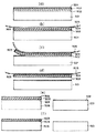
本実施形態の半導体部材の製造方法は、基板の少なくとも主面側に多孔質層を形成する工程、該多孔質層表面上にフィルムを貼り付ける工程、該多孔質層において基板側とフィルム側に分離する工程、を有する。以下図1を用いて説明する。
【0085】
まず、第1のSi単結晶基板101を用意して、主表面層に多孔質Si層102を形成する(図1(a))。多孔質Si表面にフレキシブルな粘着性フィルム103、あるいは接着剤を介してフレキシブルなフィルムを貼り付ける(図1(b))。なお、導電性ペーストを用いて貼り付けることも勿論可能である。この点は後述する実施形態例についても同様である。その後、フレキシブルなフィルムを第1のSi単結晶基板101から剥がして(図1(c))、多孔質Si層を境に基板側とフィルム側に分離する。こうして、多孔質Si薄膜を基板101から分離することができる(図1(d))。このようにして得られたフィルム103上の多孔質Si層102は、発光素子、ガス吸着センサー等に応用可能である。
【0086】
Si単結晶基板101は残留多孔質Siを除去して、Si単結晶基板として再使用できる。表面平坦性が許容できないほど荒れている場合には表面平坦化を行った後、Si単結晶基板として再使用できる。
【0087】
[実施形態例2]
ここでは第1の基体の少なくとも主面側に多孔質層を形成する工程、該多孔質層上に非多孔質層を形成する工程、該非多孔質層表面上にフィルムを貼り付ける工程、該多孔質層において、非多孔質層を第1の基板よりフィルム側に分離する工程、を有する。以下図2を用いて説明する。
【0088】
まず、第1のSi単結晶基板201を用意して、主表面層に多孔質Si層202を形成する(図2(a))。多孔質Si表面に非多孔質層203を形成する(図2(b))。非多孔質層表面にフレキシブルな粘着性フィルム204、あるいは接着剤を介してフレキシブルなフィルムを貼り付ける(図2(c))。その後、フレキシブルなフィルムを第1のSi単結晶基板201から剥がす方向に力を加えると(図2(d))、多孔質Si層を境に第1の基板側より非多孔質層及び多孔質Si層をフィルム側に分離することができる。こうして、多孔質Si/非多孔質層は基板201から分離される(図2(e))。分離された多孔質Si/非多孔質層は、発光素子、センサー等に応用可能である。
【0089】
第1のSi単結晶基板201は残留多孔質Siを除去して、第1のSi単結晶基板として再使用できる。表面平坦性が許容できないほど荒れている場合には表面平坦化を行った後、第1のSi単結晶基板として再使用できる。
【0090】
[実施形態例3]
ここでは、第1の基体の少なくとも主面側に表面は非多孔質を保持した状態で内部に多孔質層を形成する工程、該非多孔質な第1基体の表面上にフィルムを貼り付ける工程、該多孔質層を境に第1の基板側とフィルム側に分離する工程、を有する。以下図3を用いて説明する。
【0091】
まず、第1のSi単結晶基板301を用意して、主表面層側からイオン注入により内部に多孔質状のイオン注入層302を形成する(図3(a))。第1の基板は、前もって表面に非多孔質層を形成したものを用いてもよい。すなわち、基板上に前もって非多孔質材料を堆積すること等も可能である。また、非多孔質層はイオン注入後さらに形成してもよい。イオン注入に先立ち、主表面層にSiO2等の保護膜を形成しておいた方が表面荒れを予防するという点から好ましい。第1のSi基板の主表面にフレキシブルな粘着性フィルム304、あるいは接着剤を介してフレキシブルなフィルムを貼り付ける(図3(b))。その後、フレキシブルなフィルムを第1のSi単結晶基板301から剥がすと(図3(c))、多孔質状のイオン注入層を境に第1の基板側とフィルム側とに分離できる。こうして、表面の非多孔質層303を基板301から分離することができる(図3(d))。
【0092】
第1のSi単結晶基板301は残留多孔質Siを除去して、第1のSi単結晶基板として再使用できる。表面平坦性が許容できないほど荒れている場合には表面平坦化を行った後、第1のSi単結晶基板として再使用できる。
【0093】
[実施形態例4]
ここでは、多孔質半導体層と、非多孔質半導体層と、を有して構成される第1の基板上にフィルムを貼り付ける工程、前記フィルムを前記第1の基板から剥がす方向の力を前記フィルムに加えることにより前記非多孔質半導体層を前記多孔質層において前記第1の基板より分離する工程、及び分離された前記非多孔質半導体層を第2の基板に貼り合わせる工程、を有する形態について図4、図5を参照しながら説明する。
【0094】
まず、多孔質半導体層2002と非多孔質半導体層2003を有する第1の基板(図4(C))を用意する。第1の基板は、例えば単結晶シリコン基板2000(図4(A))を多孔質化して多孔質層2002を形成(図4(B))した後、該多孔質層2002上に非多孔質半導体層2003(例えばエピタキシャルSi)を形成(図4(C))して構成することもできるし、上述の第1の基板についての項で説明したようにマイクロバブルを生じさせるイオン注入技術を使用して構成することもできる。
【0095】
次いで第1の基板の非多孔質半導体層2003が形成された側にフィルム2005を貼り付ける(図4(D))。ここでフィルム2005を貼り付ける面は、非多孔質半導体層2003であっても良いし、非多孔質半導体層2003表面に形成されたSiO2 層(例えば熱酸化膜)やSiN層等の絶縁層表面であっても良い。これら非多孔質半導体層2003上に形成する層は、得ようとする半導体部材に要求される特性に応じて適宜選択して形成することができる。
【0096】
次に、フィルム2005を引き剥がす方向の力をフィルム2005に加えることにより第1の基板を分離する(図4(E))。分離された単結晶シリコン基板2000を含む基板は、多孔質半導体層(Si)2002を除去(図4(Z1))して、単結晶シリコン基板2000として再生(図4(Z2))し、次の半導体部材製造の原材料とすることができる(図4(Z2)→(A))。
【0097】
分離されたもう一方の非多孔質半導体層2003を含むフィルム2005側の基板の処理の仕方は、図5に示すように、大きく分けると3通りに大別される。W1 〜W4 に示した態様は、フィルム2005の反対側に残留する多孔質半導体層2002を除去して、非多孔質半導体層2003を第2の基板2200に貼り合わせ、次いでフィルム2005を除去するものである。X1 〜X6 及びY1 〜Y5 に示した態様は、フィルム2005の反対側表面にある部材(例えば非多孔質半導体層2003、非多孔質半導体層2002等)の表面を支持部材(フィルム、シート、あるいは基板等)2100と貼り合わせた後、フィルム2005を除去、フィルム2005を除去することによって表出する非多孔質半導体層2003を第2の基板2200に貼り合わせた後、支持部材2100を除去するものである。X1 〜X6に示した態様とY1 〜Y5 に示した態様の違いは、多孔質半導体層2002を支持部材2100との貼り合わせの前に除去する(図5(X2 ))か、あるいは、貼り合わせ後に除去する(図5(Y5 ))かである。ここに示した態様例を用いると、SOI基板や、センサー、太陽電池、液晶画像表示装置等の半導体部材を製造することができる。
【0098】
[実施形態例5]
ここでは第1の基板の少なくとも主面側に多孔質層を形成する工程、該多孔質層上に非多孔質層を形成する工程、該非多孔質層表面上にフィルムを貼り付ける工程、該多孔質層を境に第1の基板側とフィルム側に分離する工程、フィルム側の多層構造体を別の支持部材(あるいはフィルム等)上に移し替える工程、該移し替えた多層構造体の非多孔質層の表面側を第2の基体に貼り合わせる工程、該多層構造体の多孔質層を除去する工程、を有する形態について説明する。
【0099】
ここで、フィルム側の多層構造体を別の支持部材(あるいはフィルム等)上に移し替える工程、及び該移し替えた多層構造体の非多孔質層の表面側を第2の基体に貼り合わせる工程は、フィルムの粘着力(または接着力)よりも高い粘着力(または接着力)をもつ支持部材に貼り合わせてフィルムを剥し、その後フィルムが剥がれた多層構造体の非多孔質層の表面側を第2の基板に貼り合わせることで行うことができる。その後、別の支持部材(あるいは別のフィルム等)を引き剥がす(別のフィルムをエッチングで除去してもよい)。
【0100】
また、紫外線を照射することにより粘着力が弱まるフィルムを用いて、第1の基板から単層、または多層構造体を剥すときには、初期の高い粘着力を利用し、それを別の台、あるいは別のフィルムに移すときには紫外線を照射し、粘着力を弱めて構造体から剥がしてもよい。
【0101】
なお、別の支持部材等を用いなくても、液体中でフィルムをエッチングにより溶かす、あるいは、上記紫外線で弱粘着になるフィルムを用い、紫外線照射により粘着力を落として液体中で剥がす。その後、メッシュ、網等で残った多層構造体をすくい、第2の基板上に置くことで、多層構造体の非多孔質層の表面側を第2の基体に貼り合わせることができる。
【0102】
以上述べた工程は他の実施形態例についても同様に採用できるものである。
【0103】
以下図6を用いて説明する。
【0104】
第1のSi単結晶基板401を用意して、主表面層に多孔質Si層402を形成する(図6(a))。多孔質Si表面に少なくとも1層の非多孔質層403を形成する(図6(b))。非多孔質403は、単結晶Si、多結晶Si、非晶質Si、あるいは、金属膜、化合物半導体薄膜、超伝導薄膜などの中から任意に選ばれる。あるいは、MOSFET等の素子構造を形成してしまっても構わない。さらに、最表面層にSiO2 404を形成しておいた方が、貼り合わせ界面を活性層から離すことが出来るという意味でもよい。非多孔質層表面にフレキシブルな粘着性フィルム405、あるいは接着剤を介してフレキシブルなフィルムを貼り付ける(図6(c))。その後、フレキシブルなフィルム405を第1のSi単結晶基板401から剥がすと(図6(d))、多孔質Si層を境に第1の基板側とフィルム側とに分離できる。こうして、多孔質Si層402/非多孔質層403/SiO2 404を基板401から分離することができる(図6(e))。
【0105】
多孔質Si402/非多孔質層403/SiO2 404をフィルム405から剥離して後、図6(f)に示すように、第2の基板406とSiO2 404の表面とを室温で密着させる。その後、陽極接合、加圧、あるいは必要に応じて熱処理、あるいはこれらの組み合わせにより貼り合わせを強固にしてもよい。
【0106】
単結晶Siを堆積した場合には、単結晶Siの表面には熱酸化等の方法で酸化Siを形成したのち貼り合わせることが好ましい。また、第2の基板は、Si基板、Si基板上に酸化Si膜を形成したもの、石英等の光透過性基板、サファイア基板などから選択することができるが、これに限定されるものではなく、貼り合わせに供される面が十分に平坦で有れば構わない。図6(f)は絶縁層404を介して貼り合わせた様子を示してあるが、非多孔質薄膜403がSiでない場合、あるいは第2の基板がSiでない場合には絶縁層404はなくてもよい。貼り合わせに際しては絶縁性の薄板をはさみ3枚重ねで貼り合わせることも可能である。
【0107】
さらに、多孔質Si層402を選択的に除去する。非多孔質薄膜が単結晶Siの場合には通常のSiのエッチング液、あるいは多孔質Siの選択エッチング液である弗酸、あるいは弗酸にアルコールおよび過酸化水素水の少なくともどちらか一方を添加した混合液、あるいは、バッファード弗酸あるいはバッファード弗酸にアルコールおよび過酸化水素水の少なくともどちらか一方を添加した混合液の少なくとも1種類を用いて、多孔質Si層402のみを無電解湿式化学エッチングして第2の基板上に予め第1の基板の多孔質上に形成した膜を残存させる。上述したように、多孔質Siの膨大な表面積により通常のSiのエッチング液でも選択的に多孔質Siのみをエッチングすることが可能である。あるいは、非多孔質薄膜層403を研磨ストッパーとして多孔質Si層402を選択研磨で除去する。
【0108】
化合物半導体層を多孔質上に形成している場合には化合物半導体に対してSiのエッチング速度の速いエッチング液を用いて、多孔質Si層402のみを化学エッチングして第2の基板406上に薄膜化した単結晶化合物半導体層403を残存させ形成する。あるいは、単結晶化合物半導体層403を研磨ストッパーとして多孔質Si層402を選択研磨で除去する。
【0109】
図6(g)には、本発明で得られる半導体基板が示される。第2の基板406上に非多孔質薄膜、例えば単結晶Si薄膜403が平坦に、しかも均一に薄層化されて、ウエハ全域に、大面積に形成される。第2の基板406として絶縁性基板を用いれば、こうして得られた半導体基板は、絶縁分離された電子素子作製という点から見ても好適に使用することができる。
【0110】
第1のSi単結晶基板401は残留多孔質Siを除去して、第1のSi単結晶基板あるいは第2の基板等として再使用できる。表面平坦性が許容できないほど荒れている場合には表面平坦化を行った後、第1のSi単結晶基板あるいは第2の基板等として再使用できる。尚、ここで説明した各工程は、本発明の他の実施形態例においても採用可能である。
【0111】
[実施形態例6]
ここでは、第1の基板の少なくとも主面側に表面は非多孔質層を保持した状態で内部に多孔質層を形成する工程、該非多孔質層表面上にフィルムを貼り付ける工程、該多孔質層を介して第1の基板側とフィルム側に分離する工程、フィルム側の多層構造体を別の支持部材上に移し替える工程、該移し替えた多層構造体の単結晶半導体の表面側を第2の基板に貼り合わせる工程、該多層構造体の多孔質層を除去する工程、を有する形態について図7を用いて説明する。
【0112】
まず、第1のSi単結晶基板501を用意して、主表面層側から希ガス、水素、および、窒素のうち少なくとも1種の元素をイオン注入し、内部に多孔質状のイオン注入層502を形成する(図7(a))。表面は非多孔質503を保持した状態である。それに先立ち、主表面層にSiO2 504等の保護膜を形成しておいた方が表面荒れを予防するという点から好ましい。さらに、最表面層にSiO2 504を形成しておいた方が、貼り合わせ界面を活性層から離すことが出来るという意味でもよい。
【0113】
非多孔質層表面にフレキシブルな粘着性フィルム505、あるいは接着剤を介してフレキシブルなフィルムを貼り付ける(図7(b))。その後、フレキシブルなフィルム505を第1のSi単結晶基板501から剥がすと(図7(c))、多孔質状のイオン注入層502を介して第1の基板側とフィルム側とに分離できる。こうして、多孔質状のイオン注入層502/非多孔質層503/SiO2504を基板501から分離することができる(図7(d))。
【0114】
多孔質状のイオン注入層502/非多孔質層503/SiO2 504をフィルム505から剥離した後、図7(e)に示すように、第2の基板506とSiO2 504の表面とを貼り合わせる。
【0115】
さらに、多孔質状のイオン注入層502を前述したのと同様に選択的に除去する。
【0116】
図7(f)には、本例で得られる半導体基板が示される。
【0117】
第1のSi単結晶基板501は残留多孔質状のイオン注入層を除去して、第1のSi単結晶基板あるいは第2の基板等として再使用できる。
【0118】
[実施形態例7]
ここでは、第1の基板の少なくとも主面側に、表面は非多孔質を保持した状態で内部に多孔質層を形成する工程、該非多孔質状の基体表面上に非多孔質層を形成する工程、該非多孔質層表面上にフィルムを貼り付ける工程、該多孔質層を境に第1の基板側とフィルム側に分離する工程、フィルム側の多層構造体を別の支持部材上に移し替える工程、該移し替えた多層構造体の絶縁層の表面側を第2の基体に貼り合わせる工程、該多層構造体の多孔質層を除去する工程、を有する形態について図8を用いて説明する。
【0119】
まず、第1のSi単結晶基板601を用意して、主表面層側から希ガス、水素、および、窒素のうち少なくとも1種の元素をイオン注入し、内部に多孔質状のイオン注入層602を形成する(図8(a))。表面は非多孔質603を保持した状態である。それに先立ち、主表面層にSiO2 等の保護膜を形成しておいた方が表面荒れを予防するという点から好ましい。
【0120】
さらに、第1のSi単結晶基板601の表面の非多孔質層上に少なくとも1層の非多孔質層604を形成する(図8(b))。非多孔質層表面にフレキシブルな粘着性フィルム606、あるいは接着剤を介してフレキシブルなフィルムを貼り付ける(図8(c))。その後、フレキシブルなフィルム606を第1のSi単結晶基板601から剥がすと(図8(d))、多孔質状のイオン注入層602を境に第1の基板側とフィルム側に分離できる。こうして、多孔質状のイオン注入層602/非多孔質層603/非多孔質薄膜604/SiO2 605を基板601から分離することができる(図8(e))。
【0121】
多孔質状のイオン注入層602/非多孔質層603/非多孔質薄膜604/SiO2 605をフィルム606から剥離して後、図8(f)に示すように、第2の基板607とSiO2 605の表面とを貼り合わせる。
【0122】
次いで、多孔質状のイオン注入層602を選択的に除去する。
【0123】
図8(g)には、本例で得られる半導体基板が示される。第2の基板607上に非多孔質薄膜、例えば単結晶Si薄膜603/604が平坦に、しかも均一に薄層化されて、ウエハ全域に、大面積に形成される。第2の基板607として絶縁性基板を用いれば、こうして得られた半導体基板は、絶縁分離された電子素子作製という点から見ても好適に使用することができる。
【0124】
第1のSi単結晶基板601は残留多孔質状のイオン注入層を除去して、第1のSi単結晶基板あるいは第2の基板等として再使用できる。
【0125】
[実施形態例8]
ここでは、第1の基板の少なくとも主面上に非多孔質層を形成する工程、表面は非多孔質を保持した状態で内部に多孔質層を形成する工程、該非多孔質層表面上にフィルムを貼り付ける工程、該多孔質層を介して第1の基板側とフィルム側に分離する工程、フィルム側の多層構造体を別の支持台上に移し替える工程、該移し替えた多層構造体の絶縁層の表面側を第2の基体に貼り合わせる工程、該多層構造体の多孔質層を除去する工程、を有する形態について図9を用いて説明する。
【0126】
まず、第1のSi単結晶基板701を用意して、主表面上に少なくとも1層の非多孔質層702を形成する(図9(a))。最表面層にSiO2 703を形成しておいた方が、貼り合わせ界面を活性層から離すことが出来るという意味でもよい。第1基板の主表面から希ガス、水素、および、窒素のうちの少なくとも1種の元素をイオン注入し、内部に多孔質状のイオン注入層704を形成する(図9(b))。表面は非多孔質702を保持した状態である。それに先立ち、主表面層にSiO2等の保護膜を形成しておいた方が表面荒れを予防するという点から好ましい。
【0127】
多孔質状のイオン注入層704は、第1のSi単結晶基板701と非多孔質層702との界面付近あるいは非多孔質層702内部になることが好ましい。
【0128】
非多孔質層表面にフレキシブルな粘着性フィルム705、あるいは接着剤を介してフレキシブルなフィルムを貼り付ける(図9(c))。その後、フレキシブルなフィルム705を第1のSi単結晶基板701から剥がすと(図9(d))、多孔質状のイオン注入層704を境に第1の基板側とフィルム側に分離できる。こうして、多孔質状のイオン注入層704/非多孔質層702/SiO2703を基板701から分離することができる(図9(e))。
【0129】
多孔質状のイオン注入層704/非多孔質層702/SiO2 703をフィルム705から剥離して後、図9(f)に示すように、第2の基板706とSiO2 703の表面とを貼り合わせる。
【0130】
次いで、多孔質状のイオン注入層704を選択的に除去する。
【0131】
図9(g)には、本例で得られる半導体基板が示される。第2の基板706上に非多孔質薄膜、例えば単結晶Si薄膜702が平坦に、しかも均一に薄層化されて、ウエハ全域に、大面積に形成される。第2の基板706として絶縁性基板を用いれば、こうして得られた半導体基板は、絶縁分離された電子素子作製という点から見ても好適に使用することができる。
【0132】
第1のSi単結晶基板701は残留多孔質状のイオン注入層を除去して、第1のSi単結晶基板あるいは第2の基板等として再使用できる。
【0133】
[実施形態例9]
図10に示すように、上述した各実施形態例に示した工程においてSi単結晶基板の両面に各工程を施すことにより、半導体基板を同時に2枚作製することができる。図10は、両面仕様の一例として上記実施形態例5の両面仕様を示しているが、どの実施形態例にも適用できる。図10において、801は第1のSi単結晶基板、802,803は多孔質Si層、804,805は非多孔質層、806,807はSiO2 、808,809はフレキシブルなフィルム、810,811は第2の基板(支持基板)である。
【0134】
第1のSi単結晶基板801は残留多孔質Siを除去して、第1のSi単結晶基板あるいは第2の基板等として再使用できる。表面平坦性が許容できないほど荒れている場合には表面平坦化を行った後、第1のSi単結晶基板あるいは第2の基板等として再使用できる。
【0135】
支持基板810,811の材料、厚さ等は同一でなくても良い。非多孔質薄膜804,805は、両面を同一の材料、膜厚等としなくてもよい。
【0136】
[実施形態例10]
太陽電池の製造方法に本発明を適用する例について説明する。
【0137】
ここで説明する形態例は、
(イ) 基体の少なくとも一主面側を陽極化成して該基体の表面に多孔質層を形成する工程
(ロ) 前記多孔質層の上に半導体層を形成する工程
(ハ) 前記半導体層の表面にフィルムを貼り付ける工程
及び
(ニ) 前記多孔質層を境に基体側とフィルム側とに分離し、前記半導体層を前記フィルムに移設(transfer)する工程
を有するものである。太陽電池の製造に使用するフィルムは、低耐熱性フィルムが好ましく、耐熱性温度400℃以下のものが望ましい。
【0138】
図12(a)に示すように、まずシリコン単結晶基板1201の表面層にB(ホウ素)を熱拡散により導入する。この表面層がp+ となった単結晶基板1201を、HF溶液中で陽極化成により、例えば初め低電流レベルで一定時間経過した後急に高電流レベルに引き上げて短時間化成するというふうにして多孔質化する(図12(b))。このBの熱拡散は、必須の工程ではなく、この手法を用いなくとも陽極化成は可能である。
【0139】
なお、陽極化成における多孔質化において、化成電流レベルを例えば途中で低レベルから高レベルへ変化させる等によりあらかじめ多孔質層の構造に疎密の変化を設けておくことでエピタキシャル成長後に多孔質層で分離されやすいように制御することができる。
【0140】
次に多孔質化された表面層1202の上に熱CVD法により太陽電池の活性層として必要十分な厚みのシリコン層1203を形成する(図12(c))。この時、シリコン層1203の形成時に微量のドーパントを混入させることにより活性層をp-型(あるいはn- 型)に制御することが可能である。
【0141】
活性層1203の上にp+ 層(あるいはn+ 層)1204をプラズマCVD法により堆積するか、あるいは上述の活性層1203の形成の終わりにドーパントの量を増大させることで形成する(図12(d))。
【0142】
予め、裏面電極1209として銅ペーストを印刷した高分子フィルム基板1205をシリコン単結晶基板1201上の活性層1203が形成された側に密着して貼り合わせ、オーブン(図示せず)に入れて加熱し、高分子フィルム基板1205とシリコン単結晶基板1201とを固着させる(図12(e))。
【0143】
次に高分子フィルム基板1205とシリコン単結晶基板1201との間に互いに引き離す方向に力を作用させる。すなわち、高分子フィルムの可撓性を利用してシリコン単結晶基板1201のエッジから両者を徐々に引き剥がし、多孔質層1202の部分で分離する(図12(f))。
【0144】
次いで、シリコン単結晶基板から剥離した活性層1203上に残っている多孔質層1202aを選択的に除去する。
【0145】
多孔質層が除去された活性層1203の表面にプラズマCVD法等によりn+(p+ )層1206を形成し(図12(g))、さらにその上に表面反射防止層を兼ねた透明導電膜(ITO)1207およびグリッド状の集電電極1208を真空蒸着し、太陽電池とする(図12(h))。図11には、こうして得られた太陽電池が示されている。
【0146】
シリコン単結晶基板1201は、表面に残留している多孔質層1202bを上述の方法と同様にして除去して、表面平坦性が許容できないほど荒れている場合には必要に応じて表面平坦化を行った後(図12(i))、再度図12(a)の工程に供せられる。
【0147】
[実施形態例11]
ここでは多結晶太陽電池を得る形態について説明する。実施形態10のシリコン基板1201に多結晶シリコン基板を使用し、多結晶シリコン層1203を形成するようにして実施形態10と同様の手法を採用することで多結晶シリコン太陽電池を製造することができる。
【0148】
[実施形態例12]
化合物半導体太陽電池を製造する態様について説明する。
【0149】
図13(a)に示すように、まずシリコン単結晶基板1301の表面層にB(ホウ素)を熱拡散により導入する。この表面層がp+ となった単結晶基板を、HF溶液中で陽極化成により、例えば初め低電流レベルで一定時間経過した後徐々に高電流レベルに引き上げて化成するというふうにして多孔質化する(図13(b))。
【0150】
次に多孔質化された表面層1302の上にMOCVD法により例えばn+ 層(あるいはp+ 層)1306、活性層(n- 型(あるいはp- 型))1303、p+ 層(あるいはn+ 層)1304を連続して形成する(図13(c))。
【0151】
予め裏面電極1309として銅ペーストを印刷した高分子フィルム基板1305をシリコン単結晶基板1301上の化合物半導体層1303が形成された側に密着して貼り合わせ、オーブン(図示せず)に入れて加熱し、高分子フィルム基板1305とシリコン単結晶基板1301とを固着させる(図13(d))。
【0152】
次に高分子フィルム基板1305とシリコン単結晶基板1301との間に互いに引き離す方向に力を作用させる。すなわち、高分子フィルムの可撓性を利用してシリコン単結晶基板1301のエッジから両者を徐々に引き剥がし、多孔質層1302の部分で分離する(図13(e))。
【0153】
シリコン単結晶基板から剥離した化合物半導体層1303上に残っている多孔質層1302aを化合物半導体に対してシリコンのエッチング速度の速いエッチング液を用いて選択的に除去する(図13(f))。
【0154】
多孔質層が除去された化合物半導体層1303の表面にグリッド状の集電電極1308および表面反射防止層1307を真空蒸着し、太陽電池とする(図13(g))。
【0155】
シリコン単結晶基板1301は、表面に残留している多孔質層1302bを上述の方法と同様にして除去して、表面平坦性が許容できないほど荒れている場合には必要に応じて表面平坦化を行った後(図13(h))、再度図13(a)の工程に供せられる。
【0156】
本発明の方法を太陽電池の製造方法に適用する場合、基板と薄膜結晶半導体層とを接着させる方法としては銅ペーストあるいは銀ペーストのような導電性金属ペーストを前記両者の間に挿入して密着させ、焼成して固着させる方法が好適に用いられる。この場合、焼成後の銅あるいは銀等の金属は裏面電極及び裏面反射層としても機能する。また、高分子フィルム等の基板の場合には、基板と薄膜結晶半導体層を密着させた状態で(この場合、予め薄膜結晶半導体層表面に裏面電極を形成しておく)、フィルム基板の軟化点にまで温度を上げて前記両者を固着させてもよい。
【0157】
本発明の太陽電池において入射光の反射損を減らす目的で半導体層の表面にテクスチャ処理を施すことができる。シリコンの場合にはヒドラジンやNaOH、KOH等を用いて行われる。形成されるテクスチャのピラミッドの高さとしては数μm〜数十μmの範囲が適当である。
【0158】
【実施例】
以下、本発明の実施例について説明するが、本発明はこれらの実施例により何ら限定されるものではない。
【0159】
(実施例1)
単結晶Si基板の表面層をHF溶液中において陽極化成を行った。
【0160】
陽極化成条件は以下の通りであった。
【0161】
電流密度:7(mA・cm-2)
陽極化成溶液:HF:H2 O:C2 H5 OH=1:1:1
時間:11(min)
多孔質Siの厚み:12(μm)
多孔質層の表面に粘着性のフィルム(日東電工(株)製剥離テープNo.3200A)を貼り付けた後、裏面を真空チャックで固定した。次いでこの粘着性のフィルムをウエハから引き剥がした。これによって、多孔質Siが分離され、フィルム側に、多孔質Si層が残った。このような多孔質Si層は、発光素子に応用可能である。
【0162】
また、第1の基板側に残った多孔質Siもその後、49%弗酸と30%過酸化水素水との混合液で攪はんしながら選択エッチングする。その後、水素アニール、あるいは表面研磨等の表面処理を施して再び第1の基板として再投入することができた。
【0163】
(実施例2)
単結晶Si基板の表面層をHF溶液中において陽極化成を行った。
【0164】
陽極化成条件は以下の通りであった。
【0165】
電流密度:7(mA・cm-2)
陽極化成溶液:HF:H2 O:C2 H5 OH=1:1:1
時間:11(min)
多孔質Siの厚み:12(μm)
この基板を酸素雰囲気中400℃で1時間酸化した。この酸化により多孔質Siの孔の内壁は熱酸化膜で覆われた。多孔質Si上にCVD(Chemical Vapor Deposition)法により単結晶Siを0.15μmエピタキシャル成長した。成長条件は以下の通りである。
【0166】
ソースガス:SiH2 Cl2 /H2
ガス流量:0.5/180 l/min
ガス圧力:80Torr
温度:950℃
成長速度:0.3μm/min
単結晶Si表面に粘着性のフィルム(日東電工(株)製剥離テープBT−315)を貼り付けた後、基板裏面を真空チャックに固定した。次いでこの粘着性のフィルムをウエハから引き剥がした。これによって、多孔質Siが分割され、フィルム側に、エピタキシャル層と多孔質Si層が残った。
【0167】
その後、フィルム側に残った多孔質Siを49%弗酸と30%過酸化水素水との混合液で攪はんしながら選択エッチングしてもよい。そうすると、単結晶Siはエッチングされずに残り、単結晶Siをエッチ・ストップの材料として、多孔質Siは選択エッチングされ、完全に除去された。
【0168】
非多孔質Si単結晶の該エッチング液に対するエッチング速度は、極めて低く、多孔質層のエッチング速度との選択比は105以上にも達し、非多孔質層におけるエッチング量(数十オングストローム程度)は実用上無視できる膜厚減少である。
【0169】
透過電子顕微鏡による断面観察の結果、Si層には新たな結晶欠陥は導入されておらず、良好な結晶性が維持されていることが確認された。
【0170】
また、第1の基板側に残った多孔質Siもその後、49%弗酸と30%過酸化水素水との混合液で攪はんしながら選択エッチングする。その後、水素アニール、あるいは表面研磨等の表面処理を施して再び第1の基板として再投入することができた。
【0171】
(実施例3)
単結晶Si基板の表面層をHF溶液中において陽極化成を行った。
【0172】
陽極化成条件は以下の通りであった。
【0173】
電流密度:7(mA・cm-2)
陽極化成溶液:HF:H2 O:C2 H5 OH=1:1:1
時間:4(min)
多孔質Siの厚み:4.5(μm)
さらに、
電流密度:30(mA・cm-2)
陽極化成溶液:HF:H2 O:C2 H5 OH=1:1:1
時間:1(min)
多孔質Siの厚み:〜4(μm)
上記条件で、多孔度(porosity)の異なる二層構成の多孔質Si層が形成された。この陽極化成により、30(mA・cm-2)による多孔質Si層の多孔度(porosity) は大きくなり、構造的に脆弱な層が形成された。
【0174】
この基板を酸素雰囲気中400℃で1時間酸化した。この酸化により多孔質Siの孔の内壁は熱酸化膜で覆われた。多孔質Si上にCVD(Chemical Vapor Deposition)法により単結晶Siを0.15μmエピタキシャル成長した。成長条件は以下の通りである。
【0175】
ソースガス:SiH2 Cl2 /H2
ガス流量:0.5/180 l/min
ガス圧力:80Torr
温度:950℃
成長速度:0.3μm/min
単結晶Si表面に粘着性のフィルム(日東電工(株)製剥離テープNo.31RH)を貼り付けた後、裏面を真空チャックに固定した。次いでこの粘着性のフィルムをウエハから引き剥がした。これによって、多孔度の大きい脆弱な多孔質Siを境にして分割され、フィルム側に、エピタキシャル層と多孔質Si層がウエハから分離された。
【0176】
その後、フィルム側に残った多孔質Siを49%弗酸と30%過酸化水素水との混合液で攪はんしながら選択エッチングした。そうすると、単結晶Siはエッチングされずに残り、単結晶Siをエッチ・ストップの材料として、多孔質Siは選択エッチングされ、完全に除去された。
【0177】
透過電子顕微鏡による断面観察の結果、Si層には新たな結晶欠陥は導入されておらず、良好な結晶性が維持されていることが確認された。
【0178】
また、第1の基板側に残った多孔質Siもその後、49%弗酸と30%過酸化水素水との混合液で攪はんしながら選択エッチングした。その後、水素アニールを施して再び第1の基板として再投入することができた。
【0179】
(実施例4)
抵抗無指定の単結晶Si基板の表面層に拡散法により高濃度不純物層たるP+高濃度層を5μm形成した。同時に裏面にもP+ 高濃度層が形成された。高濃度表面層側からHF溶液中において陽極化成を行った。
【0180】
陽極化成条件は以下の通りであった。
【0181】
電流密度:7(mA・cm-2)
陽極化成溶液:HF:H2 O:C2 H5 OH=1:1:1
時間:11(min)
多孔質Siの厚み:12(μm)
多孔質Si層は2層構造になった。下部の多孔質Siは表層部に比較して微細な脆弱構造を有していた。
【0182】
この基板を酸素雰囲気中400℃で1時間酸化した。この酸化により多孔質Siの孔の内壁は熱酸化膜で覆われた。多孔質Si上にCVD(Chemical Vapor Deposition)法により単結晶Siを0.15μmエピタキシャル成長した。成長条件は以下の通りである。
【0183】
ソースガス:SiH2 Cl2 /H2
ガス流量:0.5/180 l/min
ガス圧力:80Torr
温度:950℃
成長速度:0.3μm/min
表面に実施例3で用いたのと同じ粘着性のフィルムを貼り付けた後、実施例3と同様にしてこの粘着性のフィルムをウエハから引き剥がした。
【0184】
これによって、下層の脆弱な多孔質Siを境に分割され、フィルム側に、エピタキシャル層と多孔質Si層がウエハから分離された。
【0185】
その後、フィルム側に残った多孔質Siを49%弗酸と30%過酸化水素水との混合液で攪はんしながら選択エッチングした。そうすると、単結晶Siはエッチングされずに残り、単結晶Siをエッチ・ストップの材料として、多孔質Siは選択エッチングされ、完全に除去された。
【0186】
透過電子顕微鏡による断面観察の結果、Si層には新たな結晶欠陥は導入されておらず、良好な結晶性が維持されていることが確認された。
【0187】
また、第1の基板側に残った多孔質Siもその後、49%弗酸と30%過酸化水素水との混合液で攪はんしながら選択エッチングした。その後、水素アニール、あるいは表面研磨等の表面処理を施して再び第1の基板として高濃度P+ 層の拡散工程に投入することができた。
【0188】
(実施例5)
単結晶Si基板の表面からH+ を40keVで5×1016cm-2イオン注入した。表面の0.2μmほどは、単結晶が保たれていた。この場合、表面にあらかじめSiO2 層を形成しておいた方がイオン注入による表面荒れを防ぐという観点からはよい。
【0189】
Si基板表面に実施例1で用いたのと同じフィルムを貼り付けた後、実施例1と同様にしてフィルムをウエハから引き剥がした。
【0190】
これによって、イオン注入層を境にウエハが分割され、フィルム側に、SiO2 層と単結晶Si層とイオン注入層が残った。
【0191】
その後、フィルム側のイオン注入層を49%弗酸と30%過酸化水素水との混合液で攪はんしながら選択エッチングした。そうすると、単結晶Siはエッチングされずに残り、単結晶Siをエッチ・ストップの材料として、イオン注入層は選択エッチングされ、完全に除去された。
【0192】
透過電子顕微鏡による断面観察の結果、Si層には新たな結晶欠陥は導入されておらず、良好な結晶性が維持されていることが確認された。
【0193】
また、第1の基板側に残ったイオン注入層もその後、49%弗酸と30%過酸化水素水との混合液で攪はんしながら選択エッチングした。その後、水素アニール、あるいは表面研磨等の表面処理を施して再び第1の基板として再投入することができた。
【0194】
(実施例6)
第1の単結晶Si基板の表面からH+ を20keVで5×1016cm-2イオン注入した。表面の0.1μmほどは、単結晶が保たれていた。この場合、表面にあらかじめSiO2 層を形成しておいた方がイオン注入による表面荒れを防ぐという観点からはよい。
【0195】
表面の保護SiO2 層を剥離した後、単結晶Si上にCVD(Chemical Vapor Deposition)法により単結晶Siを0.3μmエピタキシャル成長した。成長条件は以下の通りである。
【0196】
ソースガス:SiH2 Cl2 /H2
ガス流量:0.5/180 l/min
ガス圧力:80Torr
温度:950℃
成長速度:0.3μm/min
表面に実施例1で用いたのと同じフィルムを貼り付けた後、実施例1と同様にしてこのフィルムをウエハから引き剥がした。
【0197】
これによって、イオン注入層を境にウエハが分離され、フィルム側に、単結晶Si層とイオン注入層が残った。
【0198】
その後、フィルム側のイオン注入層を49%弗酸と30%過酸化水素水との混合液で攪はんしながら選択エッチングした。そうすると、単結晶Siはエッチングされずに残り、単結晶Siをエッチ・ストップの材料として、イオン注入層は選択エッチングされ、完全に除去された。
【0199】
透過電子顕微鏡による断面観察の結果、Si層には新たな結晶欠陥は導入されておらず、良好な結晶性が維持されていることが確認された。
【0200】
また、第1の基板側に残ったイオン注入層もその後、49%弗酸と30%過酸化水素水との混合液で攪はんしながら選択エッチングする。その後、水素アニール、あるいは表面研磨等の表面処理を施して再び第1の基板として再投入することができた。
【0201】
(実施例7)
第1の単結晶Si基板上にCVD(Chemical Vapor Deposition)法により単結晶Siを0.3μmエピタキシャル成長した。成長条件は以下の通りである。
【0202】
ソースガス:SiH2 Cl2 /H2
ガス流量:0.5/180 l/min
ガス圧力:80Torr
温度:950℃
成長速度:0.3μm/min
エピタキシャルSi層の表面からH+ を40keVで5×1016cm-2イオン注入した。表面の0.2μmほどは、単結晶が保たれていた。この場合、表面にあらかじめSiO2 層を形成しておいた方がイオン注入による表面荒れを防ぐという観点からはよい。
【0203】
表面に実施例2で用いたフィルムを貼り付けた後、実施例2と同様にこのフィルムをウエハから引き剥がした。
【0204】
これによって、イオン注入層を境にウエハが分割され、フィルム側に、SiO2 層と単結晶Si層とイオン注入層が残った。
【0205】
その後、フィルム側のイオン注入層を49%弗酸と30%過酸化水素水との混合液で攪はんしながら選択エッチングした。そうすると、単結晶Siはエッチングされずに残り、単結晶Siをエッチ・ストップの材料として、イオン注入層は選択エッチングされ、完全に除去された。
【0206】
透過電子顕微鏡による断面観察の結果、Si層には新たな結晶欠陥は導入されておらず、良好な結晶性が維持されていることが確認された。
【0207】
また、第1の基板側に残ったイオン注入層もその後、49%弗酸と30%過酸化水素水との混合液で攪はんしながら選択エッチングする。その後、水素アニール、あるいは表面研磨等の表面処理を施して再び第1の基板として再投入することができた。
【0208】
(実施例8)
第1の単結晶Si基板の表面層をHF溶液中において陽極化成を行った。
【0209】
陽極化成条件は以下の通りであった。
【0210】
電流密度:7(mA・cm-2)
陽極化成溶液:HF:H2 O:C2 H5 OH=1:1:1
時間:11(min)
多孔質Siの厚み:12(μm)
この基板を酸素雰囲気中400℃で1時間酸化した。この酸化により多孔質Siの孔の内壁は熱酸化膜で覆われた。多孔質Si上にCVD(Chemical Vapor Deposition)法により単結晶Siを0.15μmエピタキシャル成長した。成長条件は以下の通りである。
【0211】
ソースガス:SiH2 Cl2 /H2
ガス流量:0.5/180 l/min
ガス圧力:80Torr
温度:950℃
成長速度:0.3μm/min
さらに、このエピタキシャルSi層表面に熱酸化により100nmのSiO2層を形成した。
【0212】
表面に実施例2で用いたフィルムを貼り付けた後、実施例2と同様にしてフィルムをウエハから引き剥がした。
【0213】
これによって、多孔質Siを境に基板が分離され、フィルム側に、SiO2 層とエピタキシャル層と多孔層Si層が残った。
【0214】
次にフィルム裏面の多孔質層をアクリル基板にエポキシ系の接着剤を用いて接着した後、フィルムをエッチング除去した。この後、表出したSiO2 層表面と別に用意したSi基板(第2の基板)の表面と貼り合わせた。SiO2 表面とSi基板表面は、非常に平坦であったので、常温で加圧するだけで強固に貼りついた。
【0215】
ここでは支持部材としてアクリル基板を用いたが、紫外線を照射することにより粘着力が弱まるフィルム(例えば、日東電工株式会社製)を用いて、第1の基体から単層、または多層構造体を剥すときには、初期の高い粘着力を利用し、それを別の支持台に移すことには紫外線を照射し、粘着力を弱めて構造体から剥がしてもよい。
【0216】
なお、別の支持台を用いなくても、液体中で薄膜フィルムをエッチングにより溶かす、あるいは、上記紫外線で弱粘着になるフィルムを用い、紫外線照射により粘着力を落として液体中で剥がす。その後、メッシュ、網等で残った多層構造体をすくい、第2の基板上に置くことで、多層構造体の非多孔質層の表面側を第2の基体に貼り合わせることができる。
【0217】
その後、第2の基板側に残ったアクリル基板を研削除去した後、多孔質Siを49%弗酸と30%過酸化水素水との混合液で攪はんしながら選択エッチングした。そうすると、単結晶Siはエッチングされずに残り、単結晶Siをエッチ・ストップの材料として、多孔質Siは選択エッチングされ、完全に除去された。
【0218】
すなわち、Si酸化膜上に0.1μmの厚みを持った単結晶Si層が形成できた。形成された単結晶Si層の膜厚を面内全面について100点を測定したところ、膜厚の均一性は101nm±3nmであった。
【0219】
さらに水素中で1100℃で熱処理を1時間施した。表面粗さを原子間力顕微鏡で評価したところ、5μm角の領域での平均2乗粗さはおよそ0.2nmで通常市販されているSiウエハと同等であった。
【0220】
透過電子顕微鏡による断面観察の結果、Si層には新たな結晶欠陥は導入されておらず、良好な結晶性が維持されていることが確認された。
【0221】
酸化膜は、エピタキシャル層表面でなく、第2の基板表面に形成しても、あるいは、その両者に形成しても同様の結果が得られた。
【0222】
同時に第1の基板側に残った多孔質Siもその後、49%弗酸と30%過酸化水素水との混合液で攪はんしながら選択エッチングする。その後、水素アニール、あるいは表面研磨等の表面処理を施して再び第1の基板あるいは第2の基板として再投入することができた。
【0223】
(実施例9)
第1の単結晶Si基板の表面層をHF溶液中において陽極化成を行った。
【0224】
陽極化成条件は以下の通りであった。
【0225】
電流密度:7(mA・cm-2)
陽極化成溶液:HF:H2 O:C2 H5 OH=1:1:1
時間:4(min)
多孔質Siの厚み:4.5(μm)
さらに、
電流密度:30(mA・cm-2)
陽極化成溶液:HF:H2 O:C2 H5 OH=1:1:1
時間:1(min)
多孔質Siの厚み:〜4(μm)
この陽極化成により、30(mA・cm-2)による多孔質Si層の多孔度(porosity)は大きくなり、構造的に脆弱な層が形成された。
【0226】
この基板を酸素雰囲気中400℃で1時間酸化した。この酸化により多孔質Siの孔の内壁は熱酸化膜で覆われた。多孔質Si上にCVD(Chemical Vapor Deposition)法により単結晶Siを0.3μmエピタキシャル成長した。成長条件は以下の通りである。
【0227】
ソースガス:SiH2 Cl2 /H2
ガス流量:0.5/180 l/min
ガス圧力:80Torr
温度:950℃
成長速度:0.3μm/min
さらに、このエピタキシャルSi層表面に熱酸化により200nmのSiO2層を形成した。
【0228】
SiO2 表面に実施例8と同様にフィルムを貼り付けた後、フィルムをウエハから引き剥がした。
【0229】
これによって、下層の脆弱な多孔質Siを境にウエハが分離されフィルム側に、SiO2 層とエピタキシャル層と多孔質Si層が残った。
【0230】
次いで、これ以降の工程は、実施例8と同様に行った。
【0231】
これにより、Si酸化膜上に0.2μmの厚みを持った単結晶Si層が形成できた。形成された単結晶Si層の膜厚を面内全面について100点を測定したところ、膜厚の均一性は201nm±6nmであった。
【0232】
さらに水素中で1100℃で熱処理を1時間施した。表面粗さを原子間力顕微鏡で評価したところ、5μm角の領域での平均2乗粗さはおよそ0.2nmで通常市販されているSiウエハと同等であった。
【0233】
透過電子顕微鏡による断面観察の結果、Si層には新たな結晶欠陥は導入されておらず、良好な結晶性が維持されていることが確認された。
【0234】
(実施例10)
抵抗無指定の第1の単結晶Si基板の表面層に拡散法によりP+ 高濃度層を5μm形成した。同時に裏面にもP+ 高濃度層が形成された。高濃度表面層側からHF溶液中において陽極化成を行った。
【0235】
陽極化成条件は以下の通りであった。
【0236】
電流密度:7(mA・cm-2)
陽極化成溶液:HF:H2 O:C2 H5 OH=1:1:1
時間:11(min)
多孔質Siの厚み:12(μm)
多孔質Si層は2層構造になった。下部の多孔層Si層は表層部に比較して微細な脆弱構造を有していた。
【0237】
この基板を酸素雰囲気中400℃で1時間酸化した。この酸化により多孔質Siの孔の内壁は熱酸化膜で覆われた。多孔質Si上にCVD(Chemical Vapor Deposition)法により単結晶Siを0.3μmエピタキシャル成長した。成長条件は以下の通りである。
【0238】
ソースガス:SiH2 Cl2 /H2
ガス流量:0.5/180 l/min
ガス圧力:80Torr
温度:950℃
成長速度:0.3μm/min
さらに、このエピタキシャルSi層表面に熱酸化により200nmのSiO2層を形成した。
【0239】
SiO2 表面に実施例8と同様にフィルムを貼り付けた後、フィルムをウエハから引き剥がした。
【0240】
これによって、下層の脆弱な多孔質Siを境にウエハが分離されフィルム側に、SiO2 層とエピタキシャル層と多孔質Si層が残った。
【0241】
これ以降の工程は、実施例8と同様にして行い、SOI基板を作製した。
【0242】
これにより、Si酸化膜上に0.2μmの厚みを持った単結晶Si層が形成できた。形成された単結晶Si層の膜厚を面内全面について100点を測定したところ、膜厚の均一性は201nm±6nmであった。
【0243】
さらに水素中で1100℃で熱処理を1時間施した。表面粗さを原子間力顕微鏡で評価したところ、5μm角の領域での平均2乗粗さはおよそ0.2nmで通常市販されているSiウエハと同等であった。
【0244】
透過電子顕微鏡による断面観察の結果、Si層には新たな結晶欠陥は導入されておらず、良好な結晶性が維持されていることが確認された。
【0245】
酸化膜は、エピタキシャル層表面でなく、第2の基板表面に形成しても、あるいは、その両者に形成しても同様の結果が得られた。
【0246】
同時に第1の基板側に残った多孔質Siもその後、49%弗酸と30%過酸化水素水との混合液で攪はんしながら選択エッチングした。単結晶Siはエッチングされずに残り、単結晶Siをエッチ・ストップの材料として、多孔質Siは選択エッチングされ、完全に除去され、再び第1の基板として高濃度P+ 層の拡散工程に、あるいは第2の基板として再投入することができた。
【0247】
(実施例11)
第1の単結晶Si基板の表面からH+ を40keVで5×1016cm-2イオン注入した。表面の0.2μmほどは、単結晶が保たれていた。次いでこの表面に熱酸化膜(SiO2 )を形成した。
【0248】
SiO2 表面に実施例8と同様にしてフィルムを貼り付けた後、同様にしてフィルムをウエハから引き剥がした。
【0249】
これによって、イオン注入層を境にウエハが分離されフィルム側に、SiO2層と単結晶Si層とイオン注入層が残った。次いで、これ以降の工程を実施例8と同様に行った。
【0250】
これにより、Si酸化膜上に0.2μmの厚みを持った単結晶Si層が形成できた。形成された単結晶Si層の膜厚を面内全面について100点を測定したところ、膜厚の均一性は201nm±6nmであった。
【0251】
さらに水素中で1100℃で熱処理を1時間施した。表面粗さを原子間力顕微鏡で評価したところ、5μm角の領域での平均2乗粗さはおよそ0.2nmで通常市販されているSiウエハと同等であった。
【0252】
透過電子顕微鏡による断面観察の結果、Si層には新たな結晶欠陥は導入されておらず、良好な結晶性が維持されていることが確認された。
【0253】
酸化膜は、第1基板の表面でなく、第2の基板表面に形成しても、あるいは、その両者に形成しても同様の結果が得られた。
【0254】
(実施例12)
第1の単結晶Si基板の表面からH+ を20keVで5×1016cm-2イオン注入した。表面の0.1μmほどは、単結晶が保たれていた。この場合、表面にあらかじめSiO2 層を形成しておいた方がイオン注入による表面荒れを防ぐという観点からはよい。
【0255】
表面の保護SiO2 層を剥離した後、単結晶Si上にCVD(Chemical Vapor Deposition)法により単結晶Siを0.3μmエピタキシャル成長した。成長条件は以下の通りである。
【0256】
ソースガス:SiH2 Cl2 /H2
ガス流量:0.5/180 l/min
ガス圧力:80Torr
温度:950℃
成長速度:0.3μm/min
さらに、このエピタキシャルSi層表面に熱酸化により200nmのSiO2層を形成した。
【0257】
SiO2 表面に実施例8と同様にフィルムを貼り付けた後、実施例8と同様にしてフィルムをウエハから引き剥がした。
【0258】
これによって、イオン注入層を境にウエハが分離されフィルム側に、SiO2層と単結晶Si層とイオン注入層が残った。次いでこれ以降の工程を実施例8と同様に行った。
【0259】
これにより、Si酸化膜上に0.2μmの厚みを持った単結晶Si層が形成できた。形成された単結晶Si層の膜厚を面内全面について100点を測定したところ、膜厚の均一性は201nm±6nmであった。
【0260】
さらに水素中で1100℃で熱処理を1時間施した。表面粗さを原子間力顕微鏡で評価したところ、5μm角の領域での平均2乗粗さはおよそ0.2nmで通常市販されているSiウエハと同等であった。
【0261】
透過電子顕微鏡による断面観察の結果、Si層には新たな結晶欠陥は導入されておらず、良好な結晶性が維持されていることが確認された。
【0262】
酸化膜は、第1の基板の表面でなく、第2の基板表面に形成しても、あるいは、その両者に形成しても同様の結果が得られた。
【0263】
同時に第1の基板側に残ったイオン注入層もその後、49%弗酸と30%過酸化水素水との混合液で攪はんしながら選択エッチングした。その後、水素アニール、あるいは表面研磨等の表面処理を施して再び第1の基板あるいは第2の基板として再投入することができた。
【0264】
(実施例13)
第1の単結晶Si基板上にCVD(Chemical Vapor Deposition)法により単結晶Siを0.3μmエピタキシャル成長した。成長条件は以下の通りである。
【0265】
ソースガス:SiH2 Cl2 /H2
ガス流量:0.5/180 l/min
ガス圧力:80Torr
温度:950℃
成長速度:0.3μm/min
エピタキシャルSi層の表面からH+ を40keVで5×1016cm-2イオン注入した。表面の0.2μmほどは、単結晶が保たれていた。この場合、表面にあらかじめSiO2 層を形成しておいた方がイオン注入による表面荒れを防ぐという観点からはよい。
【0266】
さらに、このエピタキシャルSi層表面に熱酸化により200nmのSiO2層を形成した。
【0267】
SiO2 表面に実施例8と同様にフィルムを貼り付けた後、実施例8と同様にしてフィルムをウエハから引き剥がした。
【0268】
これによって、イオン注入層を境にウエハが分離されフィルム側に、SiO2層と単結晶Si層とイオン注入層が残った。次いでこれ以降の工程を実施例8と同様に行った。
【0269】
こうして、Si酸化膜上に0.2μmの厚みを持った単結晶Si層が形成できた。形成された単結晶Si層の膜厚を面内全面について100点を測定したところ、膜厚の均一性は201nm±6nmであった。
【0270】
さらに水素中で1100℃で熱処理を1時間施した。表面粗さを原子間力顕微鏡で評価したところ、5μm角の領域での平均2乗粗さはおよそ0.2nmで通常市販されているSiウエハと同等であった。
【0271】
透過電子顕微鏡による断面観察の結果、Si層には新たな結晶欠陥は導入されておらず、良好な結晶性が維持されていることが確認された。
【0272】
酸化膜は、第1基板の表面でなく、第2の基板表面に形成しても、あるいは、その両者に形成しても同様の結果が得られた。
【0273】
同時に第1の基板側に残ったイオン注入層もその後、49%弗酸と30%過酸化水素水との混合液で攪はんしながら選択エッチングする。その後、水素アニール、あるいは表面研磨等の表面処理を施して再び第1の基板あるいは第2の基板として再投入することができた。
【0274】
(実施例14)
第1の単結晶Si基板の表面層をHF溶液中において陽極化成を行った。
【0275】
陽極化成条件は以下の通りであった。
【0276】
電流密度:7(mA・cm-2)
陽極化成溶液:HF:H2 O:C2 H5 OH=1:1:1
時間:11(min)
多孔質Siの厚み:12(μm)
この基板を酸素雰囲気中400℃で1時間酸化した。この酸化により多孔質Siの孔の内壁は熱酸化膜で覆われた。多孔質Si上にMOCVD(Metal Organic Chemical Vapor Deposition)法により単結晶GaAsを0.5μmエピタキシャル成長した。成長条件は以下の通りである。
【0277】
ソースガス:TMG/AsH3 /H2
ガス圧力:80Torr
温度:700℃
表面に実施例1と同様のフィルムを貼り付けた後、実施例1と同様にしてフィルムをウエハから引き剥がした。
【0278】
これによって、多孔質Siを境にウエハが分離されフィルム側に、エピタキシャル層と多孔質Si層が残った。次にフィルム裏面の多孔質層をアクリル基板にエポキシ系の接着剤を用いて接着した後、フィルムをエッチング除去した。この後表出したエピタキシャル層表面と別に用意したSi基板(第2の基板)の表面とを貼り合わせた。アクリル基板を研削除去した後、第2の基板側の表面を、
エチレンジアミン+ピロカテコール+水(17ml:3g:8mlの比率)
110℃
でエッチングした。
【0279】
これにより、単結晶GaAsはエッチングされずに残り、単結晶GaAsをエッチ・ストップの材料として、イオン注入層および第1のSi基板の残りは選択エッチングされ、完全に除去された。
【0280】
その結果、Si基板上に0.5μmの厚みを持った単結晶GaAs層が形成できた。形成された単結晶GaAs層の膜厚を面内全面について100点を測定したところ、膜厚の均一性は504nm±16nmであった。
【0281】
表面粗さを原子間力顕微鏡で評価したところ、50μm角の領域での平均2乗粗さはおよそ0.3nmで通常市販されているGaAsウエハと同等であった。
【0282】
透過電子顕微鏡による断面観察の結果、GaAs層には、エピタキシャル成長時以降新たな結晶欠陥は導入されておらず、良好な結晶性が維持されていることが確認された。
【0283】
他の化合物半導体でも同様の結果が得られた。
【0284】
SiO2 層を介して第2の基板に貼り合わせることも可能である。
【0285】
同時に第1の基板側に残った多孔質Siもその後、49%弗酸と30%過酸化水素水との混合液で攪はんしながら選択エッチングした。その後、水素アニール、あるいは表面研磨等の表面処理を施して再び第1の基板あるいは第2の基板として再投入することができた。
【0286】
(実施例15)
第1の単結晶Si基板の表面層をHF溶液中において陽極化成を行った。
【0287】
陽極化成条件は以下の通りであった。
【0288】
電流密度:7(mA・cm-2)
陽極化成溶液:HF:H2 O:C2 H5 OH=1:1:1
時間:11(min)
多孔質Siの厚み:12(μm)
この基板を酸素雰囲気中400℃で1時間酸化した。この酸化により多孔質Siの孔の内壁は熱酸化膜で覆われた。多孔質Si上にCVD(Chemical Vapor Deposition)法により単結晶Siを0.15μmエピタキシャル成長した。成長条件は以下の通りである。
【0289】
ソースガス:SiH2 Cl2 /H2
ガス流量:0.5/180 l/min
ガス圧力:80Torr
温度:950℃
成長速度:0.3μm/min
さらに、このエピタキシャルSi層表面に熱酸化により100nmのSiO2層を形成した。
【0290】
SiO2 表面に実施例3で使用したのと同じフィルムを貼り付けた後、同様にフィルムをウエハから引き剥がした。
【0291】
これによって、多孔質Siを境にウエハが分離されフィルム側に、SiO2 層とエピタキシャル層と多孔層Si層が残った。その後、フィルム側に残った多孔質Siを49%弗酸と30%過酸化水素水との混合液で攪はんしながら選択エッチングした。そうすると、単結晶Siはエッチングされずに残り、単結晶Siをエッチ・ストップの材料として、多孔質Siは選択エッチングされ、完全に除去された。
【0292】
すなわち、フィルム側には0.1μm厚の単結晶Si層/0.1μm厚SiO2 層とが形成できた。
【0293】
フィルムを上記多層膜から剥がして後、該SiO2 層表面と別に用意したSi基板(第2の基板)の表面とを貼り合わせた。
【0294】
すなわち、Si酸化膜上に0.1μmの厚みを持った単結晶Si層が形成できた。形成された単結晶Si層の膜厚を面内全面について100点を測定したところ、膜厚の均一性は101nm±3nmであった。
【0295】
さらに水素中で1100℃で熱処理を1時間施した。表面粗さを原子間力顕微鏡で評価したところ、5μm角の領域での平均2乗粗さはおよそ0.2nmで通常市販されているSiウエハと同等であった。
【0296】
透過電子顕微鏡による断面観察の結果、Si層には新たな結晶欠陥は導入されておらず、良好な結晶性が維持されていることが確認された。
【0297】
酸化膜は、エピタキシャル層表面でなく、第2の基板表面に形成しても、あるいは、その両者に形成しても同様の結果が得られた。
【0298】
同時に第1の基板側に残った多孔質Siもその後、49%弗酸と30%過酸化水素水との混合液で攪はんしながら選択エッチングする。その後、水素アニール、あるいは表面研磨等の表面処理を施して再び第1の基板あるいは第2の基板として再投入することができた。
【0299】
(実施例16)
第1の単結晶Si基板の表面層をHF溶液中において陽極化成を行った。
【0300】
陽極化成条件は以下の通りであった。
【0301】
電流密度:7(mA・cm-2)
陽極化成溶液:HF:H2 O:C2 H5 OH=1:1:1
時間:11(min)
多孔質Siの厚み:12(μm)
この基板を酸素雰囲気中400℃で1時間酸化した。この酸化により多孔質Siの孔の内壁は熱酸化膜で覆われた。多孔質Si上にCVD(Chemical Vapor Deposition)法により単結晶Siを0.15μmエピタキシャル成長した。成長条件は以下の通りである。
【0302】
ソースガス:SiH2 Cl2 /H2
ガス流量:0.5/180 l/min
ガス圧力:80Torr
温度:950℃
成長速度:0.3μm/min
さらに、このエピタキシャルSi層表面に熱酸化により100nmのSiO2層を形成した。
【0303】
SiO2 層表面からH+ を100keVで3×1016cm-2イオン注入した。この投影飛程付近の陽極化成多孔質Si層の多孔度(porosity)は大きくなった。
【0304】
SiO2 表面に実施例3と同様のフィルムを貼り付けた後、同様にしてフィルムをウエハから引き剥がした。
【0305】
これによって、多孔度の大きい層(イオン注入の投影飛程付近)の多孔質Siを境にウエハが分離されフィルム側に、SiO2 層とエピタキシャル層と多孔質Si層が残った。次いでこれ以降の工程を実施例8と同様に行った。
【0306】
そうしたところSi酸化膜上に0.1μmの厚みを持った単結晶Si層が形成できた。形成された単結晶Si層の膜厚を面内全面について100点を測定したところ、膜厚の均一性は101nm±3nmであった。
【0307】
さらに水素中で1100℃で熱処理を1時間施した。表面粗さを原子間力顕微鏡で評価したところ、5μm角の領域での平均2乗粗さはおよび0.2nmで通常市販されているSiウエハと同等であった。
【0308】
透過電子顕微鏡による断面観察の結果、Si層には新たな結晶欠陥は導入されておらず、良好な結晶性が維持されていることが確認された。
【0309】
酸化膜は、エピタキシャル層表面でなく、第2の基板表面に形成しても、あるいは、その両者に形成しても同様の結果が得られた。
【0310】
同時に第1の基板側に残った多孔質Siもその後、49%弗酸と30%過酸化水素水との混合液で攪はんしながら選択エッチングした。その後、水素アニール、あるいは表面研磨等の表面処理を施して再び第1の基板あるいは第2の基板として再投入することができた。
【0311】
(実施例17)
図12に示すプロセスにより単結晶シリコン層をポリイミドフィルムに転写(transfer)して太陽電池を形成した例について示す。
【0312】
500μm厚の単結晶シリコンウエハの表面にBCl3 を熱拡散源として1200℃の温度でBの熱拡散を行ってp+ 層を形成し、3μm程度の拡散層を得た(図12(a))。次にHF溶液中で表1の条件で陽極化成を行い、ウエハ上に多孔質シリコン層を形成した(図12(b))。即ち、最初5mA/cm2 の低電流で2.5分化成した後、ゆっくりと電流レベルを上げて行き、30秒で30mA/cm2 に達したところで化成を終えた。
【0313】
【表1】

【0314】
【表2】
【0315】
厚さ50μmのポリイミドフィルムの片面にスクリーン印刷により銅ペーストを10〜30μm厚で塗り、この面を上述のウエハのp+ シリコン層面に密着させて貼り合わせた。
【0316】
この状態でオーブンに入れて360℃、20分の条件で銅ペーストの焼成を行うとともにポリイミドフィルムとウエハとを固着させた(図12(e))。
【0317】
固着したポリイミドフィルムとウエハに対して、ウエハの接着していない側の面を真空チャック(図示せず)で固定しておき、ポリイミドフィルムの一方の端から力を作用させ、ポリイミドフィルムの可撓性を利用してウエハのエッジから両者を徐々に引き剥がしてpeelingを行う。このようにしてシリコン層をウエハから剥離してポリイミドフィルム上に転写させた(図12(f))。
【0318】
シリコンウエハから剥離したシリコン層上に残っている多孔質層を、弗酸と過酸化水素水および純水との混合液で攪拌しながら選択エッチングした。シリコン層はエッチングされずに残り、多孔質層のみが完全に除去された。
【0319】
非多孔質シリコン単結晶では上述のエッチング液に対するエッチング速度は極めて低く、多孔質層のエッチング速度との選択比は105以上にも達し、非多孔質シリコン層におけるエッチング量(数十Å程度)は実用上無視できる膜厚減少である。
【0320】
透過電子顕微鏡による断面観察の結果、シリコン層には新たな結晶欠陥は導入されておらず、良好な結晶性が維持されていることが確認された。
【0321】
得られたポリイミドフィルム上のシリコン層の表面を弗酸/硝酸系のエッチング液でエッチングして清浄化を行った後、シリコン層の上に通常のプラズマCVD装置により、表3に示す条件でn型μc−Si層を200Å堆積させた(図12(g))。この時のμc−Si層の暗導電率は〜5S/cmであった。
【0322】
【表3】
【0323】
このようにして得られたポリイミド上薄膜単結晶シリコン太陽電池について、AM1.5(100mW/cm2 )の光照射下でのI−V特性について測定したところ、セル面積6cm2 で開放電圧0.6V、短絡光電流35mA/cm2 、曲線因子0.79となり、エネルギー変換効率16.6%を得た。
【0324】
また、剥離後のシリコンウエハ上に残存する多孔質層についても上述と同様にしてエッチングにより除去し、平滑な面を出した(図12(i))。こうして得られた再生ウエハを用いて上述の工程を繰り返すことにより高品質な半導体層を有する薄膜単結晶太陽電池が複数個得られた。
【0325】
(実施例18)
本実施例では図12に示すプロセスにより多結晶シリコン層をポリイミドフィルムに転写して太陽電池を形成した例について示す。
【0326】
1mm厚のキャストシリコン(多結晶シリコン)ウエハの表面にBCl3 を熱拡散源として1200℃の温度でBの熱拡散を行ってp+ 層を形成し、3μm程度の拡散層を得た(図12(a))。次にHF溶液中で表4の条件で陽極化成を行い、ウエハ上に多孔質シリコン層を形成した(図12(b))。即ち、最初5mA/cm2 の低電流で2.5分化成した後、急激に電流レベルを上げて、100mA/cm2 で8秒化成して終えた。
【0327】
【表4】
【0328】
このとき、成長中に微量のPH3 (0.数ppm〜数ppm程度)を添加して成長シリコン層をn- 型にするとともに、成長の終わりでPH3 の量を増大させて(数百ppm程度)n+ 層を形成した(図12(c)、(d))。
【0329】
【表5】
【0330】
この状態でオーブンに入れて360℃、20分の条件で銀ペーストの焼成を行うとともにポリイミドフィルムとウエハとを固着させた(図12(e))。
【0331】
固着したポリイミドフィルムとウエハに対して、ウエハの接着していない側の面を真空チャック(図示せず)で固定しておき、ポリイミドフィルムの一方の端から力を作用させ、ポリイミドフィルムの可撓性を利用してウエハのエッジから両者を徐々に引き剥がしてpeelingを行う。このようにしてシリコン層をウエハから剥離してポリイミドフィルム上に転写させた(図12(f))。
【0332】
シリコンウエハから剥離したシリコン層上に残っている多孔質層を、弗酸と過酸化水素水および純水との混合液で攪拌しながら選択エッチングした。シリコン層はエッチングされずに残り、多孔質層のみが完全に除去された。
【0333】
非多孔質シリコン多結晶では上述のエッチング液に対するエッチング速度は極めて低く、多孔質層のエッチング速度との選択比は105以上にも達し、非多孔質シリコン層におけるエッチング量(数十Å程度)は実用上無視できる膜厚減少である。
【0334】
透過電子顕微鏡による断面観察の結果、シリコン層には新たな結晶欠陥は導入されておらず、良好な結晶性が維持されていることが確認された。
【0335】
得られたポリイミドフィルム上のシリコン層の表面を弗酸/硝酸系のエッチング液でエッチングして清浄化を行った後、シリコン層の上に通常のプラズマCVD装置により、表6に示す条件でp型μc−Si層を200Å堆積させた(図12(g))。この時のμc−Si層の暗導電率は〜1 S(シーメンス)/cmであった(シーメンスはオーム(Ω)の逆数)。
【0336】
【表6】
【0337】
このようにして得られたポリイミド上薄膜多結晶シリコン太陽電池についてAM1.5(100mW/cm2 )の光照射下でのI−V特性について測定したところ、セル面積6cm2 で開放電圧0.58V、短絡光電流33mA/cm2 、曲線因子0.78となり、エネルギー変換効率14.9%を得た。
【0338】
また、剥離後のシリコンウエハ上に残存する多孔質層についても上述と同様にしてエッチングにより除去し、平滑な面を出した(図12(i))。こうして得られた再生ウエハを用いて上述の工程を繰り返すことにより高品質な半導体層を有する薄膜多結晶太陽電池が複数個得られた。
【0339】
(実施例19)
化合物半導体層をポリイミドフィルムに転写して太陽電池を形成した例を示す。
【0340】
500μm厚の単結晶シリコンウエハの表面にBCl3 を熱拡散源として1200℃の温度でBの熱拡散を行ってp+ 層を形成し、3μm程度の拡散層を得た(図13(a))。次にHF溶液中で表7の条件で陽極化成を行い、ウエハ上に多孔質シリコン層を形成した(図13(b))。即ち、最初1mA/cm2 および5mA/cm2 の低電流でそれぞれ2分および2.5分化成した後、ゆっくりと電流レベルを上げて行き、20秒で40mA/cm2 に達したところで化成を終えた。
【0341】
【表7】
【0342】
成長した最表面層のp−GaAs層の上にPd/AuをEB蒸着により形成した後に、厚さ50μm厚のポリイミドフィルムの片面にスクリーン印刷により銅ペーストを10〜30μm厚で塗り、この面を上述のウエハのGaAs/AlGaAs層側に密着させて貼り合わせた。
【0343】
この状態でオーブンに入れて370℃、20分の条件で銅ペーストの焼成を行うとともにポリイミドフィルムとウエハとを固着させた(図13(d))。
【0344】
固着したポリイミドフィルムとウエハに対して、ウエハの接着していない側の面に対して真空チャック(図示せず)で固定しておき、ポリイミドフィルムの一方の端から力を作用させ、ポリイミドフィルムの可撓性を利用してウエハのエッジから両者を徐々に引き剥がしてpeelingを行う。このようにして多孔質層のところで破壊させ、GaAs/AlGaAs層をウエハから剥離してポリイミドフィルム上に転写させた(図13(e))。
【0345】
シリコンウエハから剥離したGaAs/AlGaAs層上に残っている多孔質層を、エチレンジアミン+ピロカテコール+純水との混合液で110℃で選択エッチングした。GaAs/AlGaAs層はエッチングされずに残り、多孔質層のみが完全に除去された(図13(f))。
【0346】
単結晶GaAsの上述のエッチング液に対するエッチング速度は極めて低く、実用上無視できる膜厚減少である。
【0347】
透過電子顕微鏡による断面観察の結果、GaAs/AlGaAs層には新たな結晶欠陥は導入されておらず、良好な結晶性が維持されていることが確認された。
【0348】
得られたポリイミドフィルム上のGaAs/AlGaAs層の最表面層であるn+ GaAs層をグリッド状にエッチングしてn+ Alx Ga1-x As層を露出させ、表面電極(Au/Ge/Ni/Au)をEB蒸着およびフォトリソグラフィにより、グリッド状のn+ GaAs層の上のみに形成した後、反射防止膜としてTiO2 /MgOをプラズマCVD法により堆積して太陽電池とした(図13(g))。
【0349】
このようにして得られたポリイミドフィルム上薄膜単結晶GaAs/AlGaAs太陽電池についてAM1.5(100mW/cm2 )光照射下でのI−V特性について測定したところ、セル面積4cm2 で開放電圧2.3V、短絡光電流12.8mA/cm2 、曲線因子0.81となり、エネルギー変換効率23.8%を得た。
【0350】
また、剥離後のシリコンウエハ上に残存する多孔質層については実施例17および実施例18と同様にしてエッチングにより除去し、平滑な面を出した(図13(h))。こうして得られた再生ウエハを用いて上述の工程を繰り返すことにより高品質な半導体層を有する薄膜化合物半導体太陽電池が複数個得られた。
【0351】
(実施例20)
第1の単結晶Si基板の表面層をHF溶液中において陽極化成を行った。
【0352】
陽極化成条件は以下の通りであった。
【0353】
電流密度:7(mA・cm-2)
陽極化成溶液:HF:H2 O:C2 H5 OH=1:1:1
時間:11(min)
多孔質Siの厚み:12(μm)
この基板を酸素雰囲気中400℃で1時間酸化した。この酸化により多孔質Siの孔の内壁は熱酸化膜で覆われた。多孔質Si上にCVD(Chemical Vapor Deposition)法により単結晶Siを0.15μmエピタキシャル成長した。成長条件は以下の通りである。
【0354】
ソースガス:SiH2 Cl2 /H2
ガス流量:0.5/180 l/min
ガス圧力:80Torr
温度:950℃
成長速度:0.3μm/min
さらに、このエピタキシャルSi層表面に熱酸化により20nmのSiO2層を形成した。なお、この酸化膜は粘着性のフィルムを貼り付ける場合の保護として設けられる。
【0355】
SiO2 表面に実施例1と同様にフィルムを貼り付けた後、同様にフィルムをウエハから引き剥がした。
【0356】
これによって、多孔質Siを介して剥がれ、フィルム側に、SiO2 層とエピタキシャル層と多孔層Si層がウエハから分離された。
【0357】
その後、フィルム側に残った多孔質Siを49%弗酸と30%過酸化水素水との混合液で攪はんしながら選択エッチングした。そうすると、単結晶Siはエッチングされずに残り、単結晶Siをエッチ・ストップの材料として、多孔質Siは選択エッチングされ、完全に除去された。
【0358】
エッチングにより表出した単結晶Si層表面と表面に200nmの酸化膜を形成したSi基板の表面と貼り合わせた。
【0359】
その後フィルムはエッチングで除去することにより第2の基板に0.1μmの厚みを持った単結晶Si層が形成できた。形成された単結晶Si層の膜厚を面内全面について100点を測定したところ、膜厚の均一性は101nm±3nmであった。
【0360】
さらに水素中で1100℃−1時間熱処理を施した。表面粗さを原子間力顕微鏡で評価したところ、5μm角の領域での平均2乗粗さはおよそ0.2nmで通常市販されているSiウエハと同等であった。
【0361】
透過電子顕微鏡による断面観察の結果、Si層には新たな結晶欠陥は導入されておらず、良好な結晶性が維持されていることが確認された。
【0362】
同時に第1の基板側に残った多孔質Siもその後、49%弗酸と30%過酸化水素水との混合液で攪はんしながら選択エッチングする。その後、水素アニール、あるいは表面研磨等の表面処理を施して再び第1の基板あるいは第2の基板として再投入することができた。
【0363】
(実施例21)
第1の単結晶Si基板の表面からH+ を40keVで5×1016cm-2イオン注入した。表面の0.2μmほどは、単結晶が保たれていた。この場合、表面にあらかじめSiO2 層を形成しておいた方がイオン注入による表面荒れを防ぐという観点からはよい。
【0364】
表面に実施例3と同様にフィルムを貼り付けた後、同様にフィルムをウエハから引き剥がした。
【0365】
これによって、イオン注入層を境にウエハが分離されフィルム側に、SiO2層と単結晶Si層とイオン注入層が残った。
【0366】
その後、フィルム側に残ったイオン注入層を49%弗酸と30%過酸化水素水との混合液で攪はんしながら選択エッチングした。そうすると、単結晶Siはエッチングされずに残り、単結晶Siをエッチ・ストップの材料として、イオン注入層は選択エッチングされ、完全に除去された。
【0367】
エッチングにより表出した単結晶Si層表面と別に用意した第2の基板の表面と貼り合わせた。第2の基板としては、表面に200nmの酸化膜を形成したSi基板と石英基板の2種類を用意した。
【0368】
その後フィルムを剥がすかまたはエッチングで除去することにより第2の基板に0.2μmの厚みを持った単結晶Si層が形成できた。形成された単結晶Si層の膜厚を面内全面について100点を測定したところ、膜厚の均一性は201nm±6nmであった。
【0369】
さらに水素中で熱処理を施した。Si基板の場合は1100℃−1時間、石英基板の場合は900℃−4時間行った。表面粗さを原子間力顕微鏡で評価したところ、5μm角の領域での平均2乗粗さはおよそ0.2nmで通常市販されているSiウエハと同等であった。
【0370】
透過電子顕微鏡による断面観察の結果、Si層には新たな結晶欠陥は導入されておらず、良好な結晶性が維持されていることが確認された。
【0371】
同時に第1の基板側に残ったイオン注入層もその後、49%弗酸と30%過酸化水素水との混合液で攪はんしながら選択エッチングした。その後、水素アニール、あるいは表面研磨等の表面処理を施して再び第1の基板あるいは第2の基板として再投入することができた。
【0372】
(実施例22)
第1の単結晶Si基板の表面からH+ を20keVで5×1016cm-2イオン注入した。表面の0.1μmほどは、単結晶が保たれていた。この場合、表面にあらかじめSiO2 層を形成しておいた方がイオン注入による表面荒れを防ぐという観点からはよい。
【0373】
表面の保護SiO2 層を剥離した後、単結晶Si上にCVD(Chemical Vapor Deposition)法により単結晶Siを0.3μmエピタキシャル成長した。成長条件は以下の通りである。
【0374】
ソースガス:SiH2 Cl2 /H2
ガス流量:0.5/180 l/min
ガス圧力:80Torr
温度:950℃
成長速度:0.3μm/min
さらに、このエピタキシャルSi層表面に熱酸化により20nmのSiO2層を形成した。なお、この酸化膜は粘着性のフィルムを貼り付ける場合の保護として設けられる。
【0375】
表面に実施例3と同様にフィルムを貼り付けた後、実施例3と同様にフィルムをウエハから引き剥がした。
【0376】
これによって、イオン注入層を境にウエハが分離されフィルム側に、SiO2層と単結晶Si層とイオン注入層が残った。
【0377】
その後、フィルム側に残ったイオン注入層を49%弗酸と30%過酸化水素水との混合液で攪はんしながら選択エッチングした。そうすると、単結晶Siはエッチングされずに残り、単結晶Siをエッチ・ストップの材料として、イオン注入層は選択エッチングされ、完全に除去された。
【0378】
エッチングにより表出した単結晶Si層表面と別に用意した石英基板の表面と貼り合わせた。
【0379】
その後フィルムをエッチングで除去することにより石英基板に0.2μmの厚みを持った単結晶Si層が形成できた。形成された単結晶Si層の膜厚を面内全面について100点を測定したところ、膜厚の均一性は201nm±6nmであった。
【0380】
さらに水素中で熱処理を900℃−4時間施した。表面粗さを原子間力顕微鏡で評価したところ、5μm角の領域での平均2乗粗さはおよそ0.2nmで通常市販されているSiウエハと同等であった。
【0381】
透過電子顕微鏡による断面観察の結果、Si層には新たな結晶欠陥は導入されておらず、良好な結晶性が維持されていることが確認された。
【0382】
同時に第1の基板側に残ったイオン注入層もその後、49%弗酸と30%過酸化水素水との混合液で攪はんしながら選択エッチングした。その後、水素アニール、あるいは表面研磨等の表面処理を施して再び第1の基板あるいは第2の基板として再投入することができた。
【0383】
(実施例23)
第1の単結晶Si基板上にCVD(Chemical Vapor Deposition)法により単結晶Siを0.3μmエピタキシャル成長した。成長条件は以下の通りである。
【0384】
ソースガス:SiH2 Cl2 /H2
ガス流量:0.5/180 l/min
ガス圧力:80Torr
温度:950℃
成長速度:0.3μm/min
エピタキシャルSi層の表面からH+ を40keVで5×1016cm-2イオン注入した。表面の0.2μmほどは、単結晶が保たれていた。この場合、表面にあらかじめSiO2 層を形成しておいた方がイオン注入による表面荒れを防ぐという観点からはよい。
【0385】
さらに、このエピタキシャルSi層表面に熱酸化により20nmのSiO2層を形成した。なお、この酸化膜は粘着性のフィルムを貼り付ける場合の保護として設けられる。
【0386】
SiO2 表面に実施例3と同様にフィルムを貼り付けた後、実施例3と同様にフィルムをウエハから引き剥がした。
【0387】
これによって、イオン注入層を境にウエハが分離されフィルム側に、SiO2層と単結晶Si層とイオン注入層が残った。次いでこれ以降の工程を実施例22と同様に行った。
【0388】
こうして得られた基板の表面粗さを原子間力顕微鏡で評価したところ、5μm角の領域での平均2乗粗さはおよそ0.2nmで通常市販されているSiウエハと同等であった。
【0389】
透過電子顕微鏡による断面観察の結果、Si層には新たな結晶欠陥は導入されておらず、良好な結晶性が維持されていることが確認された。
【0390】
同時に第1の基板側に残ったイオン注入層もその後、49%弗酸と30%過酸化水素水との混合液で攪はんしながら選択エッチングした。その後、水素アニール、あるいは表面研磨等の表面処理を施して再び第1の基板あるいは第2の基板として再投入することができた。
【0391】
(実施例24)
第1の単結晶Si基板の表面からH+ を40keVで5×1016cm-2イオン注入した。表面の0.2μmほどは、単結晶が保たれていた。この場合、表面にあらかじめSiO2 層を形成しておいた方がイオン注入による表面荒れを防ぐという観点からはよい。
【0392】
表面に実施例3と同様にフィルムを貼り付けた後、同様にフィルムをウエハから引き剥がした。
【0393】
これによって、イオン注入層を境にウエハが分離されフィルム側に、SiO2層と単結晶Si層とイオン注入層がウエハから分離された。
【0394】
その後、フィルム側に残ったイオン注入層を49%弗酸と30%過酸化水素水との混合液で攪はんしながら選択エッチングした。そうすると、単結晶Siはエッチングされずに残り、単結晶Siをエッチ・ストップの材料として、イオン注入層は選択エッチングされ、完全に除去された。
【0395】
フィルムを上記多層膜から剥がした後、表出したSiO2 層表面と別に用意したSi基板(第2の基板)の表面とを貼り合わせた。
【0396】
これにより、Si酸化膜上に0.2μmの厚みを持った単結晶Si層が形成できた。形成された単結晶Si層の膜厚を面内全面について100点を測定したところ、膜厚の均一性は201nm±6nmであった。
【0397】
さらに水素中で1100℃で熱処理を1時間施した。表面粗さを原子間力顕微鏡で評価したところ、5μm角の領域での平均2乗粗さはおよそ0.2nmで通常市販されているSiウエハと同等であった。
【0398】
透過電子顕微鏡による断面観察の結果、Si層には新たな結晶欠陥は導入されておらず、良好な結晶性が維持されていることが確認された。
【0399】
酸化膜は、第1基板の表面でなく、第2の基板表面に形成しても、あるいは、その両者に形成しても同様の結果が得られた。
【0400】
また、第1の基板側に残ったイオン注入層もその後、49%弗酸と30%過酸化水素水との混合液で攪はんしながら選択エッチングした。その後、水素アニール、あるいは表面研磨等の表面処理を施して再び第1の基板あるいは第2の基板として再投入することができた。
【0401】
(実施例25)
第1の単結晶Si基板の表面からH+ を20keVで5×1016cm-2イオン注入した。表面の0.1μmほどは、単結晶が保たれていた。この場合、表面にあらかじめSiO2 層を形成しておいた方がイオン注入による表面荒れを防ぐという観点からはよい。
【0402】
表面の保護SiO2 層を剥離した後、単結晶Si上にCVD(Chemical Vapor Deposition)法により単結晶Siを0.3μmエピタキシャル成長した。成長条件は以下の通りである。
【0403】
ソースガス:SiH2 Cl2 /H2
ガス流量:0.5/180 l/min
ガス圧力:80Torr
温度:950℃
成長速度:0.3μm/min
さらに、このエピタキシャルSi層表面に熱酸化により200nmのSiO2層を形成した。
【0404】
表面に実施例2で使用したフィルムを貼り付けた後、同様にフィルムをウエハから引き剥がした。
【0405】
これによって、イオン注入層を境にウエハが分離されフィルム側に、SiO2層と単結晶Si層とイオン注入層が残った。次に、これ以降の工程を実施例24と同様に行った。
【0406】
そうしたところ、Si酸化膜上に0.2μmの厚みを持った単結晶Si層が形成できた。形成された単結晶Si層の膜厚を面内全面について100点を測定したところ、膜厚の均一性は201nm±6nmであった。
【0407】
透過電子顕微鏡による断面観察の結果、Si層には新たな結晶欠陥は導入されておらず、良好な結晶性が維持されていることが確認された。
【0408】
(実施例26)
第1の単結晶Si基板上にCVD(Chemical Vapor Deposition)法により単結晶Siを0.3μmエピタキシャル成長した。成長条件は以下の通りである。
【0409】
ソースガス:SiH2 Cl2 /H2
ガス流量:0.5/180 l/min
ガス圧力:80Torr
温度:950℃
成長速度:0.3μm/min
エピタキシャルSi層の表面からH+ を40keVで5×1016cm-2イオン注入した。表面の0.2μmほどは、単結晶が保たれていた。この場合、表面にあらかじめSiO2 層を形成しておいた方がイオン注入による表面荒れを防ぐという観点からはよい。
【0410】
さらに、このエピタキシャルSi層表面に熱酸化により200nmのSiO2層を形成した。
【0411】
表面に実施例2と同様にフィルムを貼り付けた後、同様にフィルムをウエハから引き剥がした。
【0412】
これによって、イオン注入層を境にウエハが分離されフィルム側に、SiO2層と単結晶Si層とイオン注入層が残った。次にこれ以降の工程を実施例24と同様に行った。
【0413】
これにより、Si酸化膜上に0.2μmの厚みを持った単結晶Si層が形成できた。形成された単結晶Si層の膜厚を面内全面について100点を測定したところ、膜厚の均一性は201nm±6nmであった。
【0414】
さらに水素中で1100℃で熱処理を1時間施した。表面粗さを原子間力顕微鏡で評価したところ、5μm角の領域での平均2乗粗さはおよそ0.2nmで通常市販されているSiウエハと同等であった。
【0415】
透過電子顕微鏡による断面観察の結果、Si層には新たな結晶欠陥は導入されておらず、良好な結晶性が維持されていることが確認された。
【0416】
(実施例27)
本実施例では図15に示すプロセスにより単結晶シリコン層をテフゼルフィルム(デュポン社製 透明フィルム)に転写して太陽電池を形成した例を示す。
【0417】
500μm厚の単結晶シリコンウエハの表面にBCl3 を熱拡散源として1200℃の温度でBの熱拡散を行ってp+ 層を形成し、3μm程度の拡散層を得た(図15(a))。次にHF溶液中で表8の条件で陽極化成を行い、ウエハ上に多孔質シリコン層を形成した(図15(b))。即ち、最初5mA/cm2 の低電流で2.5分化成した後、ゆっくりと電流レベルを上げて行き、30秒で30mA/cm2 に達したところで化成を終えた。
【0418】
【表8】
【0419】
【表9】
【0420】
成長終了後にn+ 層の上にEB(Electron Beam)蒸着によりITO透明導電膜(82nm)/集電電極(Ti/Pd/Ag(400nm/200nm/1μm))を形成して予め太陽電池構造を作製した後(図15(d))、厚さ80μmのテフゼルフィルムの片面に透明の接着剤を10〜30μm厚で塗り、この面を上述のウエハの透明導電膜/集電電極面に密着させて貼り合わせた(図15(e))。
【0421】
充分接着剤が硬化したところで、固着したテフゼルフィルムとウエハに対して、ウエハの接着していない側の面を真空チャック(図示せず)で固定しておき、テフゼルフィルムの一方の端から力を作用させ、テフゼルフィルムの可撓性を利用してウエハのエッジから両者を徐々に引き剥がしてpeelingを行う。このようにしてシリコン層をウエハから剥離してテフゼルフィルム上に転写させた(図15(f))。
【0422】
シリコンウエハから剥離したシリコン層上に残っている多孔質層を、弗酸と過酸化水素水および純水との混合液で攪拌しながら選択エッチングした。シリコン層はエッチングされずに残り、多孔質層のみが完全に除去された。
【0423】
得られたテフゼルフィルム上のシリコン層の裏面にスパッタ法によりAlを0.1μm付けて裏面電極とした(図15(g))。
【0424】
このようにして得られたテフゼル上薄膜単結晶シリコン太陽電池について、テフゼルフィルム側からAM1.5(100mW/cm2 )光照射したときのI−V特性について測定したところ、セル面積6cm2 で開放電圧0.59V、短絡光電流34mA/cm2 、曲線因子0.79となり、エネルギー変換効率15.8%を得た。
【0425】
また、剥離後のシリコンウエハ上に残存する多孔質層についても上述と同様にしてエッチングにより除去し、平滑な面を出した(図15(h))。こうして得られた再生ウエハを用いて上述の工程を繰り返すことにより高品質な半導体層を有する薄膜単結晶太陽電池が複数個得られた。
【0426】
(実施例28)
本実施例では図16に示すプロセスにより単結晶シリコン層を一旦樹脂フィルムに転写した後、再度シリコン層を第2の基体上に転写して太陽電池を形成する例について示す。
【0427】
500μm厚の単結晶シリコンウエハの表面にBCl3 を熱拡散源として1200℃の温度でBの熱拡散を行ってp+ 層を形成し、3μm程度の拡散層を得た(図16(a))。次にHF溶液中で表10の条件で陽極化成を行い、ウエハ上に多孔質シリコン層を形成した(図16(b))。即ち、最初5mA/cm2 の低電流で2.5分化成した後、ゆっくりと電流レベルを上げて行き、30秒で30mA/cm2 に達したところで化成を終えた。
【0428】
【表10】
【0429】
【表11】
【0430】
厚さ90μmのUV硬化型粘着フィルムの粘着面を、上述のウエハのn+層に密着させて貼り合わせた(図16(d))。
【0431】
固着した粘着フィルムとウエハに対して、ウエハの接着していない側の面を真空チャック(図示せず)で固定しておき、粘着フィルムの一方の端から力を作用させ、粘着フィルムの可撓性を利用してウエハのエッジから両者を徐々に引き剥がしてpeelingを行う。このようにしてシリコン層をウエハから剥離して粘着フィルム上に転写させた(図16(e))。
【0432】
シリコンウエハから剥離したシリコン層上に残っている多孔質層を、弗酸と過酸化水素水および純水との混合液で攪拌しながら選択エッチングした。シリコン層はエッチングされずに残り、多孔質層のみが完全に除去された。
【0433】
得られた粘着フィルム上のシリコン層の裏面にスパッタ法によりAgを0.1μm付けて裏面電極とした(図16(f))。錫/鉛半田を盛ったSUS製のバッキングプレートを上述のシリコン層の裏面電極面に接触させて、この状態で熱を加えて半田を溶かしてバッキングプレートとシリコン層を固着させた(図16(g))。
【0434】
最後にシリコン層の表面に付いている粘着フィルムに紫外線を照射して粘着性を低くしてシリコン層から剥がした後、n+層の上にEB(Electron Beam)蒸着によりITO透明導電膜(82nm)/集電電極(Ti/Pd/Ag(400nm/200nm/1μm))を形成した(図16(h))。
【0435】
このようにして2回転写により得られた薄膜単結晶シリコン太陽電池について、AM1.5(100mW/cm2 )光照射下のI−V特性について測定したところ、セル面積6cm2 で開放電圧0.6V、短絡光電流34mA/cm2 、曲線因子0.78となり、エネルギー変換効率15.9%を得た。
【0436】
また、剥離後のシリコンウエハ上に残存する多孔質層についても上述と同様にしてエッチングにより除去し、平滑な面を出した(図16(i))。こうして得られた再生ウエハを用いて上述の工程を繰り返すことにより高品質な半導体層を有する薄膜単結晶太陽電池が複数個得られた。
【0437】
(実施例29)
本実施例では図12に示すプロセスにより金属級シリコン基板上に形成したシリコン層をポリイミドフィルムに転写して太陽電池を形成した例を示す。
【0438】
なお、金属級シリコンとは不純物濃度が1ppm〜2%程度の範囲含まれるシリコンをいう。
【0439】
純度98%の金属級シリコンを原料としてCZ(Czochralski)法によりインゴットを引き上げ、0.5mm厚のウエハ状にスライスし、表面を鏡面研磨して金属級シリコン基板を作製した。作製した金属級シリコン基板の表面付近の元素分析を行ったところ、表12の結果を得た。
【0440】
【表12】
【0441】
次にHF溶液中で表13の条件で陽極化成を行い、金属級シリコン上に多孔質シリコン層を形成した(図12(b))。即ち、最初2mA/cm2 の低電流で2分化成した後、ゆっくりと電流レベルを上げて行き、1分で25mA/cm2に達し、さらにこの電流レベルで6秒保持したところで化成を終えた。
【0442】
【表13】
【0443】
このとき、成長中に微量のB2H6 (0.数ppm〜数ppm程度)を添加して成長シリコン層をp- 型にするとともに、成長の終わりでB2H6 の量を増大させて(数百ppm程度)p+ 層を形成した(図12(c)、(d))。
【0444】
【表14】
【0445】
この状態でオーブンに入れて360℃、20分の条件で銅ペーストの焼成を行うとともにポリイミドフィルムとウエハとを固着させた(図12(e))。
【0446】
固着したポリイミドフィルムとウエハに対して、ウエハの接着していない側の面を真空チャック(図示せず)で固定しておき、ポリイミドフィルムの一方の端から力を作用させ、ポリイミドフィルムの可撓性を利用してウエハのエッジから両者を徐々に引き剥がしてpeelingを行う。このようにしてシリコン層を金属級シリコン基板から剥離してポリイミドフィルム上に転写させた(図12(f))。
【0447】
金属級シリコン基板から剥離したシリコン層上に残っている多孔質層を、弗酸と過酸化水素水および純水との混合液で攪拌しながら選択エッチングした。シリコン層はエッチングされずに残り、多孔質層のみが完全に除去された。
【0448】
透過電子顕微鏡による断面観察の結果、シリコン層には新たな結晶欠陥は導入されておらず、良好な結晶性が維持されていることが確認された。
【0449】
得られたポリイミドフィルム上のシリコン層の表面を弗酸/硝酸系のエッチング液でエッチングして清浄化を行った後、シリコン層の上に通常のプラズマCVD装置により、前述した表3に示す条件でn型μc−Si層を200Å堆積させた(図12(g))。
【0450】
最後にμc−Si層の上にEB蒸着によりITO透明導電膜(82nm)/集電電極(Ti/Pd/Ag(400nm/200nm/1μm))を形成して太陽電池とした(図12(h))。
【0451】
このようにして得られたポリイミド上薄膜多結晶シリコン太陽電池についてAM1.5(100mW/cm2 )光照射下でのI−V特性について測定したところ、セル面積6cm2 で開放電圧0.57V、短絡光電流32mA/cm2 、曲線因子0.77となり、エネルギー変換効率14%を得た。
【0452】
また、剥離後のシリコンウエハ上に残存する多孔質層についても上述と同様にしてエッチングにより除去し、平滑な面を出した(図12(i))。こうして得られた再生ウエハを用いて上述の工程を繰り返すことにより高品質な半導体層を有する薄膜多結晶太陽電池が複数個得られた。
【0453】
(実施例30)
第1の単結晶Si基板の表面層をHF溶液中において陽極化成を行った。
【0454】
陽極化成条件は以下の通りであった。
【0455】
電流密度:7(mA・cm-2)
陽極化成溶液:HF:H2 O:C2 H5 OH=1:1:1
時間:4(min)
多孔質Siの厚み:4.5(μm)
さらに、
電流密度:30(mA・cm-2)
陽極化成溶液:HF:H2 O:C2 H5 OH=1:1:1
時間:1(min)
多孔質Siの厚み:〜4(μm)
この陽極化成により、30(mA・cm-2)による多孔質Si層の多孔度(porosity)は大きくなり、構造的に脆弱な層が形成された。
【0456】
この基板を酸素雰囲気中400℃で1時間酸化した。この酸化により多孔質Siの孔の内壁は熱酸化膜で覆われた。
【0457】
この熱処理は、あらかじめ低い温度で熱処理を行い孔の側壁に薄い酸化膜(多孔質層としての単結晶性は維持されている)を形成して孔の再配列を防止し、多孔質層の構造を安定化させるためのものである。
【0458】
次いで、この基板の多孔質層が形成された側の最表面を1.25%のHF溶液に浸して最表面に形成された薄い酸化膜を除去した。こうして得られた基板に今度は、H2 を230l/min流しながら1050℃、760Torrの条件で1分間の熱処理を施すと共に、さらにSiH4 を50sccm添加した条件で5分間の熱処理を施した。
【0459】
これは、シリコン原子を含有する原料ガスを微量、成膜チャンバー内に流すことで非常にゆっくりとした速度でシリコン膜を形成し、多孔質シリコン層の孔の最表面を閉塞させるためのものである。
【0460】
次いで、多孔質Si上にCVD(Chemical Vapor Deposition)法により単結晶Siを0.3μmエピタキシャル成長した。成長条件は以下の通りである。
【0461】
ソースガス:SiH2 Cl2 /H2
ガス流量:0.5/180 l/min
ガス圧力:80Torr
温度:950℃
成長速度:0.3μm/min
さらに、このエピタキシャルSi層表面に熱酸化により200nmのSiO2層を形成した。
【0462】
SiO2 表面に実施例8と同様にフィルムを貼り付けた後、フィルムをウエハから引き剥がした。
【0463】
これによって、下層の脆弱な多孔質Siを境にウエハが分離されフィルム側に、SiO2 層とエピタキシャル層と多孔質Si層が残った。
【0464】
次いでこれ以降の工程は、実施例8と同様に行った。
【0465】
これにより、Si酸化膜上に0.2μmの厚みを持った単結晶Si層が形成できた。形成された単結晶Si層の膜厚を面内全面について100点を測定したところ、膜厚の均一性は201nm±6nmであった。
【0466】
さらに水素中で1100℃で熱処理を1時間施した。表面粗さを原子間力顕微鏡で評価したところ、5μm角の領域での平均2乗粗さはおよそ0.2nmで通常市販されているSiウエハと同等であった。
【0467】
透過電子顕微鏡による断面観察の結果、Si層には新たな結晶欠陥は導入されておらず、良好な結晶性が維持されていることが確認された。
【0468】
【発明の効果】
以上説明したように、本発明によれば、非多孔質半導体層を分離した第1の基板に残留する多孔質層を除去することにより得られる基板を、再度第1の基板の原材料として利用することができる。この基板の再利用については、多孔質半導体層を有して構成される基板について、多孔質層を基板から分離する態様の場合にも、同様に残留する多孔質層を除去することにより得られる基板を、再度基板の原材料として利用することができる。
【0469】
本発明の半導体部材の製造方法においては、多孔質半導体層の有する脆弱性を利用して基板を分離できる。更に本発明においては、フィルムを基板に貼りつけ、フィルムを基板から剥がす方向の力をフィルムに加えることにより、基板を多孔質層において分離できる。この場合、フィルムを基板のエッジから徐々に引き剥がすと、引き剥がす力が、フィルムの引き剥がし部先端に中心的にかかるため基板の分離が容易なものとなる。
【0470】
従来のウエハ同士を貼り合わせたものを単純に機械的に分離する手法においては、ウエハが割れてしまうことがあったが、本発明の方法では、ウエハ割れはほとんど皆無となる。
【0471】
また本発明によれば、単に多孔質層の脆弱性を利用して分離を行うため、熱処理による気泡の凝集等の複雑な物理現象を考慮に入れ最適化する必要はなく、いたって単純な方法でかつ効果的な方法で基板を分割することが可能になる。
【0472】
また、本発明によれば、基板を分離して、フィルム上に前記基板を構成した一部の層を移設(transfer)できるため、種々の用途に適用した応用が可能となる。
【0473】
本発明の半導体部材の製造方法によれば、基板を再生して繰り返し使用することで材料の有効利用化が図られ、その結果、安価なSOI基板、太陽電池等の半導体部材を提供することができる。
【図面の簡単な説明】
【図1】 本発明の方法を説明するための模式的断面図である。
【図2】 本発明の方法を説明するための模式的断面図である。
【図3】 本発明の方法を説明するための模式的断面図である。
【図4】 本発明の方法を説明するための模式的断面図である。
【図5】 本発明の方法を説明するための模式的断面図である。
【図6】 本発明の方法を説明するための模式的断面図である。
【図7】 本発明の方法を説明するための模式的断面図である。
【図8】 本発明の方法を説明するための模式的断面図である。
【図9】 本発明の方法を説明するための模式的断面図である。
【図10】 本発明の方法を説明するための模式的断面図である。
【図11】 本発明の方法を太陽電池の製造方法に適用して得られる太陽電池の構造を示した概略断面図である。
【図12】 本発明の方法を太陽電池の製造方法に適用する場合の説明図である。
【図13】 本発明の方法を太陽電池の製造方法に適用する場合の説明図である。
【図14】 図13で説明した方法によって多孔質層上に形成されたGaAs/AlGaAs薄膜太陽電池の構造を示した概略断面図である。
【図15】 本発明を太陽電池の製造方法に適用した場合の説明図である。
【図16】 本発明を太陽電池の製造方法に適用した場合の説明図である。
【図17】 従来の方法を説明する為の説明図である。
【図18】 従来の方法を説明する為の説明図である。
【符号の説明】
101,201,301,401,501,601,701,801 Si基板
102,202,402,802,803 多孔質層
103,204,304,405,505,606,705,808,809 薄膜フィルム
203,303,403,503,603,604,702,804,805 非多孔質層(非多孔質薄膜)
302,502,602,704 イオン注入層
404,504,605,703,806,807 絶縁層
406,506,607,706,810,811 第2の基板
1201,1301,1401,1501,1601 結晶基板
1202,1202a,1202b,1302,1302a,1302b,1402,1502,1502a,1502b,1602,1602a,1602b 多孔質層
1103,1203,1303,1503,1603 活性層
1104,1204,1304,1504,1604 p+ 層(またはn+ 層)
1106,1206,1306,1506,1606 n+ 層(またはp+ 層)
1107,1207,1307,1508,1611 反射防止層(透明導電層)
1108,1208,1308,1509,1612 集電電極
1109,1209,1309,1510,1608 裏面電極
1403 n+ GaAs
1404 n+ Alx Ga1-x As
1405 n Al0.37Ga0.63As
1406 p Al0.37Ga0.63As
1407 p+ Alx Ga1-x As
1408 p Al0.37Ga0.63As
1409 n+ Alx Ga1-x As
1410 n Al0.37Ga0.63As
1411 n+ Al0.9 Ga0.1 As
1412 nGaAs
1413 pGaAs
1506 透明フィルム
1507 接着層
1606 UV硬化型フィルム
1607 粘着層[0001]
BACKGROUND OF THE INVENTION
The present invention provides a semiconductor integrated circuit, a semiconductor element such as a solar cell, a semiconductor laser, and a light emitting diode.Manufacturing method of semiconductor memberParticularly with a step of separating the substrateManufacturing method of semiconductor memberAbout.
[0002]
[Prior art]
The semiconductor member is known by the name of a semiconductor wafer, a semiconductor substrate, a semiconductor device, etc., and a semiconductor element formed using the semiconductor region or a state before the semiconductor element is formed. Shall be included.
[0003]
Some of such semiconductor members have a semiconductor layer on an insulator.
[0004]
The formation of single-crystal Si semiconductor layers on insulators is widely known as silicon-on-insulator (SOI) technology, and it uses many advantages that cannot be achieved with a bulk Si substrate used to fabricate ordinary Si integrated circuits. Much research has been done on what devices have. In other words, by using SOI technology,
1. Dielectric separation is easy and high integration is possible.
2. Excellent radiation resistance,
3. Floating capacitance is reduced and high speed is possible.
4). Well process can be omitted,
5. Can prevent latch-up,
6). Fully depleted field effect transistors are possible by thinning the film,
Etc. are obtained. These are detailed in, for example, the following documents. Special Issue: “Single-crystal silicon on non-single-crystal insulators”; edited by G.W. Cullen, Journal of Crystal Growth, volume 63, no 3, pp 429-590 (1983).
[0005]
Furthermore, in recent years, many reports have been made on SOI as a substrate that realizes high speed and low power consumption of MOSFETs (IEEE SOI conference 1994). Further, when the SOI structure is used, since an insulating layer is provided below the element, the element isolation process can be simplified as compared with the case where the element is formed on the bulk Si wafer, and the device process step is shortened. That is, in combination with high performance, it is expected to reduce the wafer cost and process cost in total compared to MOSFET and IC on bulk Si.
[0006]
Among these, fully depleted MOSFETs are expected to increase speed and reduce power consumption by improving driving power. The threshold voltage (Vth) of the MOSFET is generally determined by the impurity concentration of the channel portion. In the case of a fully depleted (FD) MOSFET using SOI, the depletion layer thickness is equal to the SOI film thickness. It will also be affected. Therefore, in order to produce a large scale integrated circuit with a high yield, uniformity of the SOI film thickness has been strongly desired.
[0007]
In addition, devices on compound semiconductors have high performance that cannot be obtained with Si, such as high speed and light emission. At present, most of these devices are epitaxially grown on a compound semiconductor substrate such as GaAs and fabricated therein. However, the compound semiconductor substrate has problems such as high cost, low mechanical strength, and difficulty in producing a large area wafer.
[0008]
For this reason, attempts have been made to heteroepitaxially grow compound semiconductors on Si wafers that are inexpensive, have high mechanical strength, and can produce large-area wafers.
[0009]
Research on the formation of SOI substrates has been active since the 1970s. Initially, a method of heteroepitaxially growing single-crystal Si on an insulating sapphire substrate (SOS: Sapphire on Silicon), or a method of forming an SOI structure by dielectric separation by oxidation of porous Si (FIPOS: Fully Isolation by Porous Oxidized Silicon), oxygen ion implantation was well studied.
[0010]
In the FIPOS method, an N-type Si layer is formed into an island shape by proton ion implantation (Imai et al., J. Crystal Growth, vol 63, 547 (1983)) or epitaxial growth and patterning on the surface of a P-type Si single crystal substrate. In this method, only the P-type Si substrate is made porous by anodizing in an HF solution so as to surround the Si island, and then the N-type Si island is dielectrically separated by accelerated oxidation. In this method, the separated Si region is determined before the device process, and there is a problem that the degree of freedom in device design may be limited.
[0011]
The oxygen ion implantation method is a method called SIMOX reported for the first time by K. Izumi. Oxygen ions 10 on Si wafer17-1018/ Cm2Then, annealing is performed at a high temperature of about 1320 ° C. in an argon / oxygen atmosphere. As a result, oxygen ions implanted with a depth corresponding to the projected range (Rp) of ion implantation are combined with Si to form an oxidized Si layer. At that time, the Si layer made amorphous by oxygen ion implantation above the oxidized Si layer is also recrystallized into a single crystal Si layer. The defects included in the Si layer on the surface are 10Five/ Cm2The amount of oxygen implantation was 4 × 10¹⁷/ Cm2By making it close, -102/ Cm2Has been successfully reduced. However, since the range of implantation energy and implantation amount that can maintain the film quality of the Si oxide layer, the crystallinity of the surface Si layer, etc. is narrow, the film thickness of the surface Si layer and buried oxide layer (BOX: Burried Oxide) is It was limited to a specific value. In order to obtain a surface Si layer having a desired film thickness, it is necessary to perform sacrificial oxidation or epitaxial growth. In that case, there is a problem that the uniformity of film thickness deteriorates as a result of the deterioration due to these processes being superimposed on the film thickness distribution.
[0012]
In addition, SIMOX has been reported to have a poorly formed Si oxide formation region called a pipe. As one of the causes, foreign substances such as dust at the time of injection are considered. In the portion where the pipe exists, the device characteristics deteriorate due to the leak between the active layer and the support substrate.
[0013]
As described above, the SIMOX ion implantation has a larger implantation amount than the ion implantation used in the normal semiconductor process, so that even if a dedicated apparatus is developed, the implantation time is long. Since ion implantation is performed by raster scanning an ion beam having a predetermined current amount or expanding the beam, an increase in implantation time is assumed as the area of the wafer increases. Further, it has been pointed out that problems such as occurrence of slip due to temperature distribution in the wafer become more severe in high-temperature heat treatment of a large area wafer. In SIMOX, a heat treatment at a high temperature not normally used in the Si semiconductor process at 1320 ° C. is essential, and there is a concern that the importance of this problem will be further increased including the development of the apparatus.
[0014]
In addition to the conventional SOI formation method as described above, in recent years, an Si structure is formed by bonding a Si single crystal substrate to another thermally oxidized Si single crystal substrate using heat treatment or an adhesive. The method is attracting attention. This method requires a uniform thinning of the active layer for the device. That is, it is necessary to reduce the thickness of a Si single crystal substrate having a thickness of several hundred μm to the order of μm or less. There are three types of thinning methods as follows.
[0015]
(1). Thinning by polishing
(2). Thinning by local plasma etching
(3). Thinning by selective etching
In the polishing of (1), it is difficult to make a thin film uniformly. In particular, when the thickness of the sub-μm is reduced, the variation becomes several tens of percent, and this uniformity is a big problem. Further, as the wafer diameter increases, the difficulty increases only.
[0016]
In the method (2), the film thickness is reduced to about 1 to 3 μm by the method (1) in advance and the film thickness distribution is measured at multiple points over the entire surface. After this, based on this film thickness distribution, SF with a diameter of several mm6Etching while correcting the film thickness distribution by scanning the plasma using the above, etc., to reduce the film thickness to a desired film thickness. It has been reported that this method can achieve a film thickness distribution of about ± 10 nm. However, if there is a foreign substance (particle) on the substrate during plasma etching, this foreign substance becomes an etching mask, and thus a protrusion is formed on the substrate.
[0017]
In addition, since the surface is rough immediately after etching, touch polishing is necessary after the plasma etching is completed. However, since the amount of polishing is controlled by time management, the final film thickness is controlled by the polishing and the film thickness by polishing. Deterioration of the distribution is pointed out. Further, in polishing, an abrasive such as colloidal silica directly rubs the surface that becomes the active layer, so there is a concern about formation of a crushed layer by polishing and introduction of processing strain. Further, when the wafer area is increased, the plasma etching time increases in proportion to the increase in the wafer area, and there is a concern that the throughput may be significantly reduced.
[0018]
The method (3) is a method in which a film structure that can be selectively etched is formed in advance on a substrate to be thinned. For example, boron on a P-type substrate is 1019/ CmThreeP contained in the above concentration+A thin layer of -Si and a thin layer of P-type Si are stacked by a method such as epitaxial growth to form a first substrate. After this is bonded to the second substrate through an insulating layer such as an oxide film, the back surface of the first substrate is thinned in advance by grinding and polishing. After that, P etching is performed by selective etching of the P-type layer.+Layer exposed, and P+The P-type layer is exposed by selective etching of the layer to complete the SOI structure. This method is detailed in Maszara's report (W. P. Maszara, J. Electrochem. Soc., Vol. 138, 341 (1991)).
[0019]
Selective etching is effective for uniform thinning,
・ No more than 102And the selectivity is not enough.
[0020]
-Since the surface property after etching is poor, touch polishing is required after etching. However, as a result, the film thickness decreases, and the film thickness uniformity tends to deteriorate. In particular, in polishing, the polishing amount is managed according to time. However, since the polishing rate varies greatly, it is difficult to control the polishing amount. Therefore, there is a particular problem in forming an ultrathin SOI layer of 100 nm.
[0021]
The crystallinity of the SOI layer is poor because ion implantation, epitaxial growth on the heavily doped B-doped Si layer or heteroepitaxial growth is used. Moreover, the surface properties of the surfaces to be bonded are also inferior to those of ordinary Si wafers.
(C. Harendt, et.al., J. Elect. Mater. Vol. 20, 267 (1991), H. Baumgart, et.al., Extended Abstract of ECS 1st International Symposium of Wafer Bonding, pp. -733 (1991), CEHunt, Extended Abstract of ECS 1st International Symposium of Wafer Bonding, pp-696 (1991)). The selectivity of the selective etching largely depends on the concentration difference of impurities such as boron and the steepness of the profile in the depth direction. Therefore, if high-temperature bonding annealing for increasing the bonding strength or high-temperature epitaxial growth for improving crystallinity is performed, the depth distribution of the impurity concentration expands and the etching selectivity deteriorates. In other words, it has been difficult to improve both the bonding strength and the crystallinity of the etching selectivity.
[0022]
Under such circumstances, the present applicant previously proposed a method for manufacturing a new semiconductor member in Japanese Patent Laid-Open No. 5-21338. The method disclosed in the publication is as follows. That is, a member in which a non-porous single crystal semiconductor region is arranged on a porous single crystal semiconductor region is formed, and the surface of the member made of an insulating material is formed on the surface of the non-porous single crystal semiconductor region. After the bonding, the method for producing a semiconductor member is characterized in that the porous single crystal semiconductor region is removed by etching.
[0023]
In addition, Yonehara et al., The inventor of the present invention, reported a bonded SOI that has excellent film thickness uniformity and crystallinity and can be batch-processed (T.Yonehara et.al., Appl.Phys.Lett.vol). .64,2108 (1994)). Hereinafter, a method for manufacturing the bonded SOI will be described with reference to FIGS.
[0024]
In this method, the
[0025]
In the conventional method, the etching selectivity is based on the difference in impurity concentration and the profile in the depth direction, so the temperature of heat treatment (bonding, epitaxial growth, oxidation, etc.) that expands the concentration distribution is largely limited to approximately 800 ° C. or less. It was. On the other hand, it has been reported that the etching in this method has a heat treatment temperature of about 1180 ° C. because the difference in structure between the porous and the bulk determines the etching speed, so that the heat treatment temperature is limited. For example, heat treatment after bonding is known to increase the bonding strength between wafers and reduce the number and size of voids generated at the bonding interface. Further, in the etching based on such a structural difference, even if there are particles adhering to the porous Si, the film thickness uniformity is not affected.
[0026]
However, a semiconductor substrate using bonding always requires two wafers, one of which is mostly removed and discarded by polishing, etching, etc., and limited earth resources are wasted. It has become. Therefore, in the SOI by bonding, in addition to its controllability and uniformity, it is desired to reduce costs and improve economy.
[0027]
That is, there has been a demand for a method for manufacturing an SOI substrate with sufficient quality with good reproducibility, and simultaneously realizing resource saving and cost reduction by reusing a wafer.
[0028]
Under these circumstances, the present applicant bonded the two substrates first, then separated the bonded substrates in the porous layer, removed the residual porous material from one of the separated substrates, and removed the substrate. A method of manufacturing a semiconductor substrate to be reused was proposed in Japanese Patent Laid-Open No. 7-302889.
[0029]
One example of the method disclosed in the publication will be described below with reference to FIGS.
[0030]
After the surface layer of the
[0031]
In the invention disclosed in Japanese Patent Laid-Open No. 7-302889, the substrate is separated by utilizing the point that the structure of the porous silicon layer is weaker than that of non-porous silicon. Since the substrate used in the process can be used again for the manufacturing process of the semiconductor substrate, it is very useful in reducing the cost of the semiconductor substrate.
[0032]
Apart from this, Japanese Patent Application Laid-Open No. 8-213645 discloses that a semiconductor layer constituting a photoelectric conversion part of a solar cell is formed on a porous silicon layer and then the semiconductor layer is separated from the porous layer. Again, it is shown that the substrate on which the porous silicon layer has been formed is reused.
[0033]
In the method disclosed in Japanese Patent Application Laid-Open No. 8-213645, the semiconductor layer is bonded to a rigid jig through an adhesive, while the silicon substrate on which the porous silicon layer is formed is attached to another jig ( After bonding to the rigid body, the semiconductor layer is separated from the porous layer by pulling the jigs in opposite directions. In this method, a force that peels the entire surface of the wafer at a stretch is required to separate the rigid bodies. Therefore, if the wafer diameter increases, an external force proportional to the square must be applied.
[0034]
In addition, because it is difficult to control the force due to lack of flexibility, it is difficult to divide in the desired area.
[0035]
By the way, the solar cell is desired to be able to form an element on a low-cost substrate because of cost requirements. On the other hand, silicon is generally used as a semiconductor constituting the solar cell. Among these, single crystal silicon is most excellent from the viewpoint of efficiency of converting light energy into electromotive force, that is, photoelectric conversion efficiency. However, amorphous silicon is advantageous from the viewpoint of increasing the area and cost. In recent years, the use of polycrystalline silicon has been studied for the purpose of obtaining the cost as low as amorphous silicon and the high energy conversion efficiency as high as single crystal.
[0036]
However, the conventional methods proposed for such single crystals and polycrystalline silicon slice the massive crystals into a plate-like substrate, and it was difficult to reduce the thickness to 0.3 mm or less. . Therefore, since the substrate has a thickness more than necessary to sufficiently absorb the light amount, the effective use of the material has not been sufficient. That is, further reduction in thickness is necessary to reduce the price. Recently, a method of forming a silicon sheet by a spin method in which molten silicon droplets are poured into a mold has been proposed. However, the thickness is at least about 0.1 mm to 0.2 mm, which is necessary and sufficient for light absorption as crystalline silicon. Is still not sufficiently thin compared to a large film thickness (20 μm to 50 μm).
[0037]
Therefore, there has been proposed an attempt to achieve high energy conversion efficiency and low cost by separating (separating) the thin film epitaxial layer grown on the single crystal silicon substrate from the substrate and using it in a solar cell ( Milnes, AGand Feucht, DL, “Peeled Film Technology Solar Cells”, IEEE Photovoltaic Specialist Conference, p.338, 1975).
[0038]
However, in this method, it is necessary to insert a SiGe intermediate layer between the single crystal silicon used as a substrate and the growth epitaxial layer to perform heteroepitaxial growth, and then selectively melt this intermediate layer to peel off the growth layer. is there. In general, when heteroepitaxial growth is performed, defects are likely to be induced at the growth interface because of different lattice constants. Moreover, it cannot be said that it is advantageous in terms of process cost in terms of using different materials.
[0039]
In addition, the method disclosed in U.S. Pat.No. 4,816,420 is characterized in that a sheet-like crystal is formed on a crystal substrate through a mask material by selective epitaxial growth and lateral growth method, and then separated from the substrate. It was shown that a thin crystalline solar cell can be obtained by the manufacturing method of the solar cell.
[0040]
However, in this method, the opening provided in the mask material is in a line shape, and in order to separate the sheet-like crystal grown by selective epitaxial growth and lateral growth from this line seed, the cleavage of the crystal is used. Therefore, if the shape of the line seed is larger than a certain size, the contact area with the substrate increases, and the sheet-like crystal is damaged during the peeling. In particular, when the area of a solar cell is to be increased, the above method is practically difficult if the line length becomes several mm to several cm or more, no matter how narrow the line width (in practice, around 1 μm). It becomes.
[0041]
In view of such points, the present applicant formed a porous silicon layer by anodization on the surface of the silicon wafer and then peeled off. The peeled porous layer was fixed on the metal substrate, and the epitaxial layer was formed on the porous layer. Japanese Unexamined Patent Publication No. 6-45622 discloses a method for producing a solar cell that can be used to obtain a thin-film crystalline solar cell having good characteristics.
[0042]
However, even in this method, since the metal substrate is exposed to a high temperature process, there is a possibility that impurities are mixed in the epitaxial layer, which is not always perfect.
On the other hand, although different from such a porous layer, a separation technique using a bubble layer is disclosed in Japanese Patent Application Laid-Open No. 5-211128 as performing a substantially similar function. In this publication, a bubble layer is formed in a silicon substrate by ion implantation, crystal rearrangement and bubble aggregation are caused by heat treatment in the bubble layer, and the region on the outermost surface side of the silicon substrate ( In this publication, it is called “thin semiconductor material film”) with the bubble layer as a boundary.
[0043]
The thin semiconductor material film here is a region where the implanted ions on the outermost surface of the bulk Si are not present or are present in an extremely small amount.
[0044]
However, this method needs to be performed at a temperature at which crystal rearrangement and bubble agglomeration occur effectively, and it is not easy to establish ion implantation conditions and optimize heat treatment.
[0045]
An object of the present invention is to provide a method of manufacturing a semiconductor member having a step of separating a substrate, wherein a part of the substrate can be reused as a raw material of the semiconductor member.
[0046]
[Means for Solving the Problems]
The method for producing a semiconductor member of the present invention includes a step of attaching a flexible film on a substrate configured to include a porous semiconductor layer and a non-porous semiconductor layer provided on the porous semiconductor layer. wearpastingProcess,
SaidBy applying a force in the direction of peeling the film from the substrate to the film, the non-porous semiconductor layer is gradually peeled off from the edge of the substrate in the porous semiconductor layer and separated from the substrate.SeparationProcess,
It is characterized by having.
[0048]
In the present inventionThe substrate obtained by removing the porous layer remaining on the first substrate from which the non-porous semiconductor layer has been separated can be used again as a raw material for the first substrate. This reuse of the substrate is obtained by removing the remaining porous layer in the same manner in the case where the porous layer is separated from the substrate with respect to the substrate configured with the porous semiconductor layer. The obtained substrate can be used again as a raw material of the substrate.
[0049]
In the method for producing a semiconductor member of the present invention, the substrate is separated using the vulnerability of the porous semiconductor layer. Furthermore, in this invention, a board | substrate is isolate | separated in a porous layer by sticking a film to a board | substrate and applying the force of the direction which peels a film from a board | substrate to a film. In this case, when the film is gradually peeled off from the edge of the substrate, the peeling force is applied mainly to the tip of the peeling portion of the film, so that the substrate can be easily separated.
[0050]
In the conventional method of simply mechanically separating the bonded wafers, the wafer may break, but in the method of the present invention, there is almost no wafer cracking.
[0051]
Further, according to the present invention, since the separation is performed simply using the vulnerability of the porous layer, there is no need to optimize in consideration of complicated physical phenomena such as agglomeration of bubbles due to heat treatment. It is possible to divide the substrate in an effective and effective manner.
[0052]
In addition, according to the present invention, since the substrate is separated and a part of the layer constituting the substrate can be transferred onto the film, applications applicable to various uses are possible.
[0053]
According to the method for manufacturing a semiconductor member of the present invention, the material can be effectively used by regenerating and repeatedly using the substrate. As a result, an inexpensive semiconductor member such as an SOI substrate or a solar cell can be provided. it can.
[0054]
DETAILED DESCRIPTION OF THE INVENTION
Hereinafter, preferred embodiments of the present invention will be described, but the present invention is not limited to these embodiments, and any object can be used as long as the object of the present invention can be achieved.
[0055]
[Porous semiconductor layer]
As the porous semiconductor layer, one using silicon (Si) is preferably used.
[0056]
Porous Si was discovered by Uhlir et al. In 1956 in the research process of electrolytic polishing of semiconductors (A. Uhlir, Bell Syst. Tech. J., vol. 35, 333 (1956)). Porous Si can be formed by anodizing a Si substrate in an HF solution. Unagami et al. Studied the dissolution reaction of Si in anodization, and reported that holes were necessary for the anodic reaction of Si in HF solution, and the reaction was as follows (T. Unagami, J. Electrochem. Soc., Vol. 127, 476 (1980)).
[0057]
Si + 2HF + (2-n) e+→ SiF2+ 2H++ Ne-
SiF2+ 2HF → SiFFour+ H2
SiFFour+ 2HF → H2SiF6
Or
Si + 4HF + (4-λ) e+→ SiFFour+ 4H++ Λe-
SiFFour+ 2HF → H2SiF6
Where e+And e-Represents holes and electrons, respectively. Further, n and λ are the number of holes necessary for dissolving Si1 atoms, respectively, and porous Si is formed when the condition of n> 2 or λ> 4 is satisfied.
[0058]
From the above, P-type Si in which holes are present is made porous and N-type Si is not made porous. However, N-type Si can also be made porous by changing the conditions.
[0059]
In the present invention, porous Si having single crystallinity can be formed by anodizing a single crystal Si substrate, for example, in an HF solution. The porous layer is 10-110 holes with a diameter of about 10 nm-1It has a sponge-like structure arranged at intervals of about 10 nm. The density is 2.33 g / cm of single crystal Si.ThreeCompared to the above, the HF solution concentration is changed to 50 to 20% or the current density is changed to 2.1 to 0.6 g / cm.ThreeThe range can be changed. That is, Porosity can be varied. In this way, the density of porous Si can be reduced to less than half that of single crystal Si, but single crystallinity is maintained, and a single crystal Si layer can be epitaxially grown on top of the porous layer. It is.
[0060]
In addition, since the porous layer has a large amount of voids formed therein, the density is reduced to less than half. As a result, since the surface area increases dramatically compared to the volume, the chemical etching rate is significantly increased as compared with the etching rate of a normal single crystal layer.
[0061]
The mechanical strength of porous Si varies with porosity, but is considered weaker than bulk Si. For example, if the porosity is 50%, the mechanical strength can be considered as half the bulk. That is, when compression, tension, or shear force is applied to the bonded wafer, the porous Si layer is first destroyed. Moreover, if the porosity is increased, the porous layer can be destroyed with a weaker force.
[0062]
In the present invention, the current density at the time of anodizing the porous layer can be changed to have a multilayer structure with different porosities. Also, a porous layer thicker than the thickness of the high concentration impurity layer can be formed by forming a high concentration impurity layer on one surface of the Si substrate and anodizing from this surface.
[0063]
When helium or hydrogen is ion-implanted into bulk Si and heat treatment is applied, a micro-cavity having a diameter of several nanometers to several tens of nanometers is 10 to 10 in the implanted region.16-17 / CmThreeIt has been reported to form at a density (eg A. Van Veen, CC Griffioen, and JHEvans, Mat. Res. Soc. Symp. Proc. 107 (1988, Material Res. Soc. Pittsburgh, Pennsylvania) p.449.). Recently, the use of these microcavities as gettering sites for metal impurities has been studied.
[0064]
V.Raineri and S.U.Campisano formed a cavity group formed by injecting helium ions into bulk Si and heat-treating, and then forming a groove in the substrate to expose the side surface of the cavity group and perform an oxidation treatment. As a result, the cavities were selectively oxidized to form a buried oxide Si layer. That is, it has been reported that an SOI structure can be formed (V. Raineri, and S. U. Campisano, Appl. Phys. Lett. 66 (1995) p. 3654). However, in their method, the thickness of the surface Si layer and the buried Si oxide layer is limited to both the formation of the cavity group and the relaxation of the stress introduced by the volume expansion during the oxidation. Therefore, it is necessary to form a groove, and an SOI structure cannot be formed on the entire surface of the substrate. The porous semiconductor layer of the present invention includes a layer having such a micro-cavity or micro-bubble.
[0065]
[the film]
As the film used in the present invention, a polyimide-based resinous adhesive film, a resinous conductive film, a metal conductive film, a film whose adhesive force changes by light, electron beam, heat, etc., or an aluminum foil containing Although glass cloth film etc. can be mentioned, it is not specifically limited to these.
[0066]
Specific examples include Tefzel film manufactured by Dupont, aluminum foil glass cloth tape (No. 363) manufactured by Scotch, heat-resistant aluminum foil tape (No. 433), and release tape manufactured by Nitto Denko Corporation ( No. 3200A, No. 31RH, BT-315) and the like.
[0067]
Further, when the film is attached to the substrate, for example, when the adhesive force is insufficient, the film can be attached using an adhesive. Adhesives such as epoxy-based adhesives, waxes, SOG (spin on glass), etc. can be used as the adhesive, or the resin component of the conductive paste can be heated and blown away to replace the adhesive. It can also be made.
[0068]
The thickness of the film of the present invention is appropriately selected according to the material and characteristics of the film to be used, but is preferably 5 μm to 3 cm, more preferably 10 μm to 1 cm.
[0069]
[Non-porous semiconductor layer]
In the present invention, as the non-porous semiconductor layer, preferably, in addition to single crystal Si, polycrystalline Si, and amorphous Si, GaAs, InP, GaAsP, GaAlAs, InAs, AlGaSb, InGaAs, ZnS, CdSe, CdTe, A compound semiconductor such as SiGe can be used. The non-porous semiconductor layer may be one in which a semiconductor element such as an FET (Field Effect Transistor) is already formed.
[0070]
[First substrate]
The first base is formed by forming the above-mentioned non-porous semiconductor layer on the porous silicon layer formed in the silicon substrate, or partially in the silicon substrate provided with the non-porous semiconductor layer. It can be configured by forming a porous silicon layer.
[0071]
Further, the first substrate is a substrate having a non-porous semiconductor layer formed on a silicon substrate in which an ion implantation layer for generating micro-bubbles is formed. A substrate in which an insulating film such as a nitride film or an oxide film is formed on a semiconductor layer, or a substrate in which an epitaxial semiconductor layer and an insulating layer are formed on a silicon substrate and then ion-implanted into the silicon substrate to form an ion-implanted layer; Furthermore, the thing etc. which formed the ion implantation layer in the non-porous semiconductor layer formed on the silicon substrate are included.
[0072]
In the present invention, the epitaxial growth method used for forming the silicon layer on the porous layer includes a thermal CVD method, an LPCVD method, a sputtering method, a plasma CVD method, a photo CVD method, a liquid phase growth method and the like. For example, a source gas used in the case of a vapor phase growth method such as a thermal CVD method, an LPCVD method, a plasma CVD method or a photo CVD method is SiH.2Cl2, SiClFour, SiHClThree, SiHFour, Si2H6, SiH2F2, Si2F6Typical examples include silanes and halogenated silanes.
[0073]
Further, hydrogen (H) is added to the source gas as a carrier gas or for the purpose of obtaining a reducing atmosphere for promoting crystal growth.2) Is added. The ratio of the amount of the source gas and hydrogen is appropriately determined according to the formation method, the type of the source gas, and the formation conditions, but is preferably 1:10 or more and 1: 1000 or less (introduction flow ratio). Preferably it is 1:20 or more and 1: 800 or less.
[0074]
H when using liquid phase growth2Or N2Epitaxial growth is performed by dissolving silicon in a solvent such as Ga, In, Sb, Bi, or Sn in an atmosphere and slowly cooling the solvent or setting a temperature difference in the solvent.
[0075]
When a compound semiconductor layer is formed on the porous layer, MOCVD method, MBE method, liquid phase growth method or the like is used. The raw material used for these crystal growth methods is appropriately determined depending on the type of compound semiconductor to be formed and each growth method. For example, when forming GaAs, the MOCVD method uses Ga (CHThree)Three, AsHThree, Al (CHThree)ThreeIn the liquid phase growth, the solvent is Ga, and As or As and Al are dissolved in the solvent to perform the growth.
[0076]
The temperature and pressure in the epitaxial growth method used in the present invention vary depending on the forming method and the type of raw material (gas) used, but the temperature is about 800 when silicon is grown by a normal thermal CVD method, for example. It is desirable that the temperature is not lower than 1 ° C and not higher than 1250 ° C, and more preferably controlled at 850 ° C or higher and 1200 ° C or lower. In the case of the liquid phase growth method, depending on the type of the solvent, when silicon is grown using Sn or In as a solvent, it is desirable that the temperature is controlled at 600 ° C. or higher and 1050 ° C. or lower. When growing GaAs using Ga as a solvent, it is desirable to control the temperature to 650 ° C. or higher and 850 ° C. or lower. When GaAs is grown by the MOCVD method, it is desirable to control the temperature to 650 ° C. or higher and 900 ° C. or lower. In a low-temperature process such as a plasma CVD method, the temperature is generally 200 ° C. or higher and 600 ° C. or lower, and more preferably 200 ° C. or higher and 500 ° C. or lower.
[0077]
Similarly, the pressure is approximately 10 except for the MBE method.-2Torr to 760 Torr is suitable, more preferably 10-1The range of Torr to 760 Torr is desirable. When using the MBE method, the exhaust pressure is 10-FiveTorr or less is suitable, more preferably 10-6Torr or less is desirable.
[0078]
[Second substrate]
Examples of the second substrate to which the non-porous semiconductor layer is transferred include a semiconductor substrate such as a single crystal silicon substrate, and an insulating film such as an oxide film (including a thermal oxide film) or a nitride film on the surface of the semiconductor substrate. , A light-transmitting substrate such as a quartz substrate or a glass substrate, a sheet-like resin or metal substrate, an insulating substrate such as alumina, and the like. Such a 2nd base | substrate is suitably selected according to the use of a semiconductor member.
[0079]
[Lamination of non-porous semiconductor layer and second substrate]
In the present invention, the non-porous semiconductor layer on the above-mentioned film is bonded to the above-mentioned second substrate (so that the non-porous semiconductor layer is located inside) to obtain a multilayer structure. In the present invention, the multilayer structure in which the non-porous semiconductor layer is located on the inside is, of course, a structure in which the non-porous semiconductor layer on the film separated from the first substrate is directly bonded to the second substrate. This also includes a structure in which an insulating film such as an oxide film or a nitride film formed on the surface of the non-porous semiconductor layer, or a film other than this is bonded to the second substrate. That is, a structure in which the nonporous semiconductor layer is positioned inside the multilayer structure compared to the film or the support member is referred to as a multilayer structure in which the nonporous semiconductor layer is positioned inside.
[0080]
The specific bonding can be performed by keeping the bonding surface of the non-porous semiconductor layer and the second substrate flat, and bringing them into close contact, for example, at room temperature. In addition, in order to increase the bonding strength, anodic bonding, pressurization, heat treatment, and the like can be performed.
[0081]
[Removal of porous layer]
After the multilayer structure obtained by bonding the first substrate and the second substrate is separated in the porous Si layer, the porous Si layer remaining on the separated substrate is the mechanical strength of the porous Si layer. Can be selectively removed by taking advantage of its low surface area and its very large surface area. As a selective removal method, a mechanical method using grinding or polishing, a chemical etching method using an etching solution, or an ion etching method (for example, reactive ion etching) can be employed.
[0082]
When the porous Si layer is selectively etched using an etching solution, the etching solution is not limited to a mixed solution of 49% hydrofluoric acid and 30% hydrogen peroxide solution, but is a mixture of hydrofluoric acid and hydrofluoric acid with alcohol added thereto. Liquid, a mixture of alcohol and hydrogen peroxide in hydrofluoric acid, a mixture of buffered hydrofluoric acid, alcohol in buffered hydrofluoric acid, a mixture of hydrogen peroxide in buffered hydrofluoric acid, buffer A mixed solution obtained by adding alcohol and hydrogen peroxide to dehydrofluoric acid, or a mixed solution of hydrofluoric acid, nitric acid, and acetic acid can be employed. After selectively removing the porous layer, the flatness of the nonporous semiconductor layer can be increased by heat-treating the semiconductor member obtained by transferring the nonporous semiconductor layer in an atmosphere containing hydrogen.
[0083]
Hereinafter, embodiments of the present invention will be specifically described with reference to the drawings.
[0084]
[Embodiment 1]
The method for producing a semiconductor member of the present embodiment includes a step of forming a porous layer on at least a main surface side of a substrate, a step of attaching a film on the surface of the porous layer, and a substrate side and a film side in the porous layer. Separating. This will be described below with reference to FIG.
[0085]
First, a first Si
[0086]
The Si
[0087]
[Embodiment 2]
Here, a step of forming a porous layer on at least the main surface side of the first substrate, a step of forming a non-porous layer on the porous layer, a step of attaching a film on the surface of the non-porous layer, the porous The porous layer has a step of separating the non-porous layer from the first substrate to the film side. This will be described below with reference to FIG.
[0088]
First, a first Si
[0089]
The first Si
[0090]
[Embodiment 3]
Here, a step of forming a porous layer in the state in which the surface is kept non-porous on at least the main surface side of the first substrate, a step of attaching a film on the surface of the non-porous first substrate, Separating the first substrate side and the film side with the porous layer as a boundary. This will be described below with reference to FIG.
[0091]
First, a first Si
[0092]
The first Si
[0093]
[Embodiment 4]
Here, the step of attaching a film on a first substrate comprising a porous semiconductor layer and a non-porous semiconductor layer, the force in the direction of peeling the film from the first substrate, A mode having a step of separating the non-porous semiconductor layer from the first substrate in the porous layer by adding to the film, and a step of bonding the separated non-porous semiconductor layer to the second substrate Will be described with reference to FIGS.
[0094]
First, a first substrate (FIG. 4C) including a
[0095]
Next, a
[0096]
Next, the first substrate is separated by applying a force in a direction in which the
[0097]
As shown in FIG. 5, the method of processing the substrate on the side of the
[0098]
[Embodiment 5]
Here, a step of forming a porous layer on at least the main surface side of the first substrate, a step of forming a non-porous layer on the porous layer, a step of attaching a film on the surface of the non-porous layer, the porous A step of separating the first substrate side and the film side from the porous layer, a step of transferring the multilayer structure on the film side onto another support member (or film, etc.), and the non-porous property of the transferred multilayer structure A mode having a step of bonding the surface side of the porous layer to the second substrate and a step of removing the porous layer of the multilayer structure will be described.
[0099]
Here, a step of transferring the multilayer structure on the film side onto another support member (or film or the like), and a step of bonding the surface side of the non-porous layer of the transferred multilayer structure to the second substrate Is attached to a support member having an adhesive strength (or adhesive strength) higher than the adhesive strength (or adhesive strength) of the film, peeled off the film, and then the surface side of the non-porous layer of the multilayer structure where the film is peeled off This can be done by attaching to the second substrate. Thereafter, another support member (or another film or the like) is peeled off (the other film may be removed by etching).
[0100]
In addition, when a single layer or multilayer structure is peeled from the first substrate using a film whose adhesive strength is weakened by irradiating with ultraviolet rays, the initial high adhesive strength is used, and this is applied to another stage or When transferred to the film, the film may be peeled off from the structure by irradiating with ultraviolet rays to weaken the adhesive force.
[0101]
In addition, even if it does not use another support member etc., a film is melt | dissolved in a liquid by an etching, or the film which becomes weakly adhesive by the said ultraviolet-ray is used, and adhesive force is dropped by ultraviolet irradiation and it peels in a liquid. Thereafter, the remaining multilayer structure with a mesh, net, etc. is scooped and placed on the second substrate, whereby the surface side of the non-porous layer of the multilayer structure can be bonded to the second substrate.
[0102]
The steps described above can be similarly applied to other embodiments.
[0103]
This will be described below with reference to FIG.
[0104]
A first Si single crystal substrate 401 is prepared, and a porous Si layer 402 is formed on the main surface layer (FIG. 6A). At least one non-porous layer 403 is formed on the porous Si surface (FIG. 6B). The non-porous 403 is arbitrarily selected from monocrystalline Si, polycrystalline Si, amorphous Si, or a metal film, a compound semiconductor thin film, a superconducting thin film, or the like. Alternatively, an element structure such as a MOSFET may be formed. Furthermore, the outermost layer is SiO2It may also mean that the formation of 404 can separate the bonding interface from the active layer. A flexible adhesive film 405 or a flexible film is attached to the surface of the non-porous layer via an adhesive (FIG. 6C). Thereafter, when the flexible film 405 is peeled off from the first Si single crystal substrate 401 (FIG. 6D), it can be separated into the first substrate side and the film side with the porous Si layer as a boundary. Thus, porous Si layer 402 / non-porous layer 403 / SiO2404 can be separated from the substrate 401 (FIG. 6E).
[0105]
Porous Si402 / Nonporous layer 403 / SiO2After peeling 404 from the film 405, as shown in FIG.2The surface of 404 is brought into close contact with the room temperature. Thereafter, the bonding may be strengthened by anodic bonding, pressurization, or heat treatment as necessary, or a combination thereof.
[0106]
In the case where single crystal Si is deposited, it is preferable that the surface of the single crystal Si be bonded together after forming the oxidized Si by a method such as thermal oxidation. The second substrate can be selected from a Si substrate, a Si substrate formed with an Si oxide film, a light-transmitting substrate such as quartz, and a sapphire substrate, but is not limited thereto. As long as the surface used for bonding is sufficiently flat. FIG. 6 (f) shows a state of bonding through the insulating layer 404, but if the non-porous thin film 403 is not Si, or if the second substrate is not Si, the insulating layer 404 is not required. Good. In bonding, it is also possible to sandwich three insulating thin plates and stack them together.
[0107]
Further, the porous Si layer 402 is selectively removed. When the non-porous thin film is single crystal Si, hydrofluoric acid that is a normal Si etching solution or porous Si selective etching solution, or at least one of alcohol and hydrogen peroxide water is added to hydrofluoric acid. Using at least one of a mixed solution or a mixed solution obtained by adding at least one of alcohol and hydrogen peroxide to buffered hydrofluoric acid or buffered hydrofluoric acid, only the porous Si layer 402 is subjected to electroless wet chemistry. The film previously formed on the porous substrate of the first substrate is left on the second substrate by etching. As described above, it is possible to selectively etch only porous Si even with a normal Si etchant due to the enormous surface area of porous Si. Alternatively, the porous Si layer 402 is removed by selective polishing using the non-porous thin film layer 403 as a polishing stopper.
[0108]
In the case where the compound semiconductor layer is formed on the porous layer, only the porous Si layer 402 is chemically etched on the second substrate 406 using an etching solution having a high Si etching rate with respect to the compound semiconductor. The thinned single crystal compound semiconductor layer 403 is formed to remain. Alternatively, the porous Si layer 402 is removed by selective polishing using the single crystal compound semiconductor layer 403 as a polishing stopper.
[0109]
FIG. 6G shows a semiconductor substrate obtained by the present invention. A non-porous thin film, for example, a single crystal Si thin film 403, is flattened and uniformly thinned on the second substrate 406 to form a large area over the entire wafer. If an insulating substrate is used as the second substrate 406, the semiconductor substrate obtained in this manner can be preferably used from the viewpoint of manufacturing an electronic element that is insulated and separated.
[0110]
The first Si single crystal substrate 401 can be reused as a first Si single crystal substrate, a second substrate, or the like after removing residual porous Si. If the surface flatness is unacceptably rough, it can be reused as the first Si single crystal substrate or the second substrate after the surface flattening. In addition, each process demonstrated here is employable also in the other embodiment of this invention.
[0111]
[Embodiment 6]
Here, a step of forming a porous layer inside with the surface holding at least a main surface side of the first substrate, a step of attaching a film on the surface of the non-porous layer, the porous Separating the first substrate side and the film side through the layers, transferring the multilayer structure on the film side onto another support member, and changing the surface side of the single crystal semiconductor of the transferred multilayer structure to the first side A mode including the step of bonding to the substrate 2 and the step of removing the porous layer of the multilayer structure will be described with reference to FIG.
[0112]
First, a first Si
[0113]
A flexible
[0114]
Porous
[0115]
Further, the porous
[0116]
FIG. 7F shows the semiconductor substrate obtained in this example.
[0117]
The first Si
[0118]
[Embodiment 7]
Here, on the at least main surface side of the first substrate, a step of forming a porous layer therein while maintaining a non-porous surface, and a non-porous layer is formed on the surface of the non-porous substrate A step of attaching a film on the surface of the non-porous layer, a step of separating the first substrate side and the film side with the porous layer as a boundary, and transferring the multilayer structure on the film side onto another support member A mode having a step, a step of bonding the surface side of the insulating layer of the transferred multilayer structure to a second substrate, and a step of removing the porous layer of the multilayer structure will be described with reference to FIG.
[0119]
First, a first Si
[0120]
Further, at least one
[0121]
Porous
[0122]
Next, the porous
[0123]
FIG. 8G shows the semiconductor substrate obtained in this example. A non-porous thin film, for example, a single crystal Si
[0124]
The first Si
[0125]
[Embodiment 8]
Here, a step of forming a non-porous layer on at least the main surface of the first substrate, a step of forming a porous layer inside the surface while maintaining the non-porous state, and a film on the surface of the non-porous layer A step of separating the first substrate side and the film side through the porous layer, a step of transferring the multilayer structure on the film side onto another support base, and A mode including the step of bonding the surface side of the insulating layer to the second substrate and the step of removing the porous layer of the multilayer structure will be described with reference to FIG.
[0126]
First, a first Si
[0127]
The porous
[0128]
A flexible
[0129]
Porous
[0130]
Next, the porous
[0131]
FIG. 9G shows the semiconductor substrate obtained in this example. A non-porous thin film, for example, a single crystal Si
[0132]
The first Si
[0133]
[Embodiment 9]
As shown in FIG. 10, two semiconductor substrates can be fabricated simultaneously by performing each step on both sides of the Si single crystal substrate in the steps shown in the above-described embodiments. FIG. 10 shows the double-sided specification of the fifth embodiment as an example of the double-sided specification, but it can be applied to any embodiment. In FIG. 10, 801 is a first Si single crystal substrate, 802 and 803 are porous Si layers, 804 and 805 are non-porous layers, and 806 and 807 are SiO.2, 808 and 809 are flexible films, and 810 and 811 are second substrates (supporting substrates).
[0134]
The first Si
[0135]
The materials and thicknesses of the
[0136]
[Embodiment 10]
The example which applies this invention to the manufacturing method of a solar cell is demonstrated.
[0137]
The form example described here is
(A) A step of anodizing at least one principal surface of the substrate to form a porous layer on the surface of the substrate
(B) forming a semiconductor layer on the porous layer
(C) A step of attaching a film to the surface of the semiconductor layer
as well as
(D) a step of separating the base layer side and the film side with the porous layer as a boundary, and transferring the semiconductor layer to the film
It is what has. The film used for manufacturing the solar cell is preferably a low heat resistant film, and preferably has a heat resistant temperature of 400 ° C. or lower.
[0138]
As shown in FIG. 12A, first, B (boron) is introduced into the surface layer of the silicon
[0139]
In addition, in anodization, the separation current is separated by a porous layer after epitaxial growth by providing a change in the density of the porous layer in advance, for example, by changing the formation current level from a low level to a high level in the middle. It can be controlled to be easy to be done.
[0140]
Next, a
[0141]
P on the
[0142]
A
[0143]
Next, force is applied between the
[0144]
Next, the porous layer 1202a remaining on the
[0145]
The surface of the
[0146]
The silicon
[0147]
[Embodiment 11]
Here, a mode for obtaining a polycrystalline solar cell will be described. A polycrystalline silicon solar cell can be manufactured by using a polycrystalline silicon substrate as the
[0148]
[Embodiment 12]
An embodiment for producing a compound semiconductor solar battery will be described.
[0149]
As shown in FIG. 13A, first, B (boron) is introduced into the surface layer of the silicon
[0150]
Next, for example, n is formed on the
[0151]
A
[0152]
Next, force is applied between the
[0153]
The porous layer 1302a remaining on the
[0154]
A grid-like current collecting electrode 1308 and a surface antireflection layer 1307 are vacuum-deposited on the surface of the
[0155]
The silicon
[0156]
When the method of the present invention is applied to a method for manufacturing a solar cell, a conductive metal paste such as a copper paste or a silver paste is inserted between the substrate and the thin film crystalline semiconductor layer so as to adhere to each other. And a method of fixing by baking is preferably used. In this case, the fired metal such as copper or silver also functions as a back electrode and a back reflection layer. In the case of a substrate such as a polymer film, the softening point of the film substrate with the substrate and the thin film crystal semiconductor layer in close contact (in this case, a back electrode is formed in advance on the surface of the thin film crystal semiconductor layer). The both may be fixed by raising the temperature.
[0157]
In the solar cell of the present invention, the surface of the semiconductor layer can be textured for the purpose of reducing the reflection loss of incident light. In the case of silicon, hydrazine, NaOH, KOH or the like is used. The height of the texture pyramid to be formed is suitably in the range of several μm to several tens of μm.
[0158]
【Example】
Examples of the present invention will be described below, but the present invention is not limited to these examples.
[0159]
Example 1
The surface layer of the single crystal Si substrate was anodized in an HF solution.
[0160]
The anodizing conditions were as follows.
[0161]
Current density: 7 (mA · cm-2)
Anodizing solution: HF: H2O: C2HFiveOH = 1: 1: 1
Time: 11 (min)
Thickness of porous Si: 12 (μm)
After sticking an adhesive film (Nitto Denko Co., Ltd. release tape No. 3200A) on the surface of the porous layer, the back surface was fixed with a vacuum chuck. The adhesive film was then peeled from the wafer. Thereby, porous Si was separated, and a porous Si layer remained on the film side. Such a porous Si layer can be applied to a light emitting device.
[0162]
The porous Si remaining on the first substrate side is then selectively etched while being stirred with a mixed solution of 49% hydrofluoric acid and 30% hydrogen peroxide. Thereafter, hydrogen annealing or surface treatment such as surface polishing was performed, and the substrate was again input again.
[0163]
(Example 2)
The surface layer of the single crystal Si substrate was anodized in an HF solution.
[0164]
The anodizing conditions were as follows.
[0165]
Current density: 7 (mA · cm-2)
Anodizing solution: HF: H2O: C2HFiveOH = 1: 1: 1
Time: 11 (min)
Thickness of porous Si: 12 (μm)
This substrate was oxidized in an oxygen atmosphere at 400 ° C. for 1 hour. Due to this oxidation, the inner walls of the porous Si holes were covered with a thermal oxide film. Single-crystal Si was epitaxially grown to a thickness of 0.15 μm on the porous Si by a CVD (Chemical Vapor Deposition) method. The growth conditions are as follows.
[0166]
Source gas: SiH2Cl2/ H2
Gas flow rate: 0.5 / 180 l / min
Gas pressure: 80 Torr
Temperature: 950 ° C
Growth rate: 0.3 μm / min
After sticking an adhesive film (Nitto Denko Co., Ltd. release tape BT-315) on the single crystal Si surface, the back surface of the substrate was fixed to a vacuum chuck. The adhesive film was then peeled from the wafer. Thereby, porous Si was divided, and an epitaxial layer and a porous Si layer remained on the film side.
[0167]
Thereafter, the porous Si remaining on the film side may be selectively etched while being stirred with a mixed solution of 49% hydrofluoric acid and 30% hydrogen peroxide. Then, the single crystal Si remained without being etched, and the porous Si was completely removed by selective etching using the single crystal Si as an etch stop material.
[0168]
The etching rate of the non-porous Si single crystal with respect to the etching solution is extremely low, and the selectivity with respect to the etching rate of the porous layer is 10FiveThe etching amount in the non-porous layer (several tens of angstroms) is a reduction in film thickness that can be ignored in practice.
[0169]
As a result of cross-sectional observation with a transmission electron microscope, it was confirmed that no new crystal defects were introduced into the Si layer and that good crystallinity was maintained.
[0170]
The porous Si remaining on the first substrate side is then selectively etched while being stirred with a mixed solution of 49% hydrofluoric acid and 30% hydrogen peroxide. Thereafter, hydrogen annealing or surface treatment such as surface polishing was performed, and the substrate was again input again.
[0171]
(Example 3)
The surface layer of the single crystal Si substrate was anodized in an HF solution.
[0172]
The anodizing conditions were as follows.
[0173]
Current density: 7 (mA · cm-2)
Anodizing solution: HF: H2O: C2HFiveOH = 1: 1: 1
Time: 4 (min)
Porous Si thickness: 4.5 (μm)
further,
Current density: 30 (mA · cm-2)
Anodizing solution: HF: H2O: C2HFiveOH = 1: 1: 1
Time: 1 (min)
Porous Si thickness: ~ 4 (μm)
Under the above conditions, a porous Si layer having a two-layer structure with different porosities was formed. By this anodization, 30 (mA · cm-2), The porosity of the porous Si layer was increased, and a structurally fragile layer was formed.
[0174]
This substrate was oxidized in an oxygen atmosphere at 400 ° C. for 1 hour. Due to this oxidation, the inner walls of the porous Si holes were covered with a thermal oxide film. Single-crystal Si was epitaxially grown to a thickness of 0.15 μm on the porous Si by a CVD (Chemical Vapor Deposition) method. The growth conditions are as follows.
[0175]
Source gas: SiH2Cl2/ H2
Gas flow rate: 0.5 / 180 l / min
Gas pressure: 80 Torr
Temperature: 950 ° C
Growth rate: 0.3 μm / min
After sticking an adhesive film (Nitto Denko Co., Ltd. release tape No. 31RH) on the single crystal Si surface, the back surface was fixed to a vacuum chuck. The adhesive film was then peeled from the wafer. As a result, the fragile porous Si having a large porosity was divided as a boundary, and the epitaxial layer and the porous Si layer were separated from the wafer on the film side.
[0176]
Thereafter, the porous Si remaining on the film side was selectively etched while stirring with a mixed solution of 49% hydrofluoric acid and 30% hydrogen peroxide. Then, the single crystal Si remained without being etched, and the porous Si was completely removed by selective etching using the single crystal Si as an etch stop material.
[0177]
As a result of cross-sectional observation with a transmission electron microscope, it was confirmed that no new crystal defects were introduced into the Si layer and that good crystallinity was maintained.
[0178]
The porous Si remaining on the first substrate side was then selectively etched while stirring with a mixed solution of 49% hydrofluoric acid and 30% hydrogen peroxide. After that, hydrogen annealing was performed, and it was possible to input again as the first substrate.
[0179]
(Example 4)
A high-concentration impurity layer is formed on the surface layer of a single crystal Si substrate with no resistance specified by a diffusion method.+A high concentration layer was formed to 5 μm. At the same time P on the back+A high concentration layer was formed. Anodization was performed in the HF solution from the high concentration surface layer side.
[0180]
The anodizing conditions were as follows.
[0181]
Current density: 7 (mA · cm-2)
Anodizing solution: HF: H2O: C2HFiveOH = 1: 1: 1
Time: 11 (min)
Thickness of porous Si: 12 (μm)
The porous Si layer has a two-layer structure. The lower porous Si had a fine fragile structure as compared with the surface layer portion.
[0182]
This substrate was oxidized in an oxygen atmosphere at 400 ° C. for 1 hour. Due to this oxidation, the inner walls of the porous Si holes were covered with a thermal oxide film. Single-crystal Si was epitaxially grown to a thickness of 0.15 μm on the porous Si by a CVD (Chemical Vapor Deposition) method. The growth conditions are as follows.
[0183]
Source gas: SiH2Cl2/ H2
Gas flow rate: 0.5 / 180 l / min
Gas pressure: 80 Torr
Temperature: 950 ° C
Growth rate: 0.3 μm / min
After the same adhesive film as used in Example 3 was attached to the surface, the adhesive film was peeled off from the wafer in the same manner as in Example 3.
[0184]
Thus, the lower fragile porous Si was divided as a boundary, and the epitaxial layer and the porous Si layer were separated from the wafer on the film side.
[0185]
Thereafter, the porous Si remaining on the film side was selectively etched while stirring with a mixed solution of 49% hydrofluoric acid and 30% hydrogen peroxide. Then, the single crystal Si remained without being etched, and the porous Si was completely removed by selective etching using the single crystal Si as an etch stop material.
[0186]
As a result of cross-sectional observation with a transmission electron microscope, it was confirmed that no new crystal defects were introduced into the Si layer and that good crystallinity was maintained.
[0187]
The porous Si remaining on the first substrate side was then selectively etched while stirring with a mixed solution of 49% hydrofluoric acid and 30% hydrogen peroxide. After that, surface treatment such as hydrogen annealing or surface polishing was performed, and the substrate was again put into the diffusion process of the high concentration P + layer.
[0188]
(Example 5)
H from the surface of the single crystal Si substrate+5 × 10 at 40 keV16cm-2Ion implantation was performed. The single crystal was maintained about 0.2 μm on the surface. In this case, SiO2 is previously formed on the surface.2From the viewpoint of preventing surface roughness due to ion implantation, it is better to form a layer.
[0189]
After the same film as used in Example 1 was attached to the Si substrate surface, the film was peeled off from the wafer in the same manner as in Example 1.
[0190]
As a result, the wafer is divided with the ion implantation layer as a boundary, and on the film side, SiO2The layer, the single crystal Si layer, and the ion implantation layer remained.
[0191]
Thereafter, the ion-implanted layer on the film side was selectively etched while stirring with a mixed solution of 49% hydrofluoric acid and 30% hydrogen peroxide. As a result, the single crystal Si remained without being etched, and the ion implantation layer was selectively removed by using the single crystal Si as an etch stop material and completely removed.
[0192]
As a result of cross-sectional observation with a transmission electron microscope, it was confirmed that no new crystal defects were introduced into the Si layer and that good crystallinity was maintained.
[0193]
The ion implantation layer remaining on the first substrate side was then selectively etched while stirring with a mixed solution of 49% hydrofluoric acid and 30% hydrogen peroxide. Thereafter, hydrogen annealing or surface treatment such as surface polishing was performed, and the substrate was again input again.
[0194]
(Example 6)
H from the surface of the first single crystal Si substrate+5 × 10 at 20 keV16cm-2Ion implantation was performed. The single crystal was maintained about 0.1 μm on the surface. In this case, SiO2 is previously formed on the surface.2From the viewpoint of preventing surface roughness due to ion implantation, it is better to form a layer.
[0195]
Surface protection SiO2After peeling off the layers, single-crystal Si was epitaxially grown on the single-crystal Si by 0.3 μm by CVD (Chemical Vapor Deposition). The growth conditions are as follows.
[0196]
Source gas: SiH2Cl2/ H2
Gas flow rate: 0.5 / 180 l / min
Gas pressure: 80 Torr
Temperature: 950 ° C
Growth rate: 0.3 μm / min
After the same film as used in Example 1 was attached to the surface, the film was peeled off from the wafer in the same manner as in Example 1.
[0197]
As a result, the wafer was separated from the ion implantation layer as a boundary, and the single crystal Si layer and the ion implantation layer remained on the film side.
[0198]
Thereafter, the ion-implanted layer on the film side was selectively etched while stirring with a mixed solution of 49% hydrofluoric acid and 30% hydrogen peroxide. As a result, the single crystal Si remained without being etched, and the ion implantation layer was selectively removed by using the single crystal Si as an etch stop material and completely removed.
[0199]
As a result of cross-sectional observation with a transmission electron microscope, it was confirmed that no new crystal defects were introduced into the Si layer and that good crystallinity was maintained.
[0200]
The ion implantation layer remaining on the first substrate side is then selectively etched while stirring with a mixed solution of 49% hydrofluoric acid and 30% hydrogen peroxide. Thereafter, hydrogen annealing or surface treatment such as surface polishing was performed, and the substrate was again input again.
[0201]
(Example 7)
Single-crystal Si was epitaxially grown to a thickness of 0.3 μm on the first single-crystal Si substrate by a CVD (Chemical Vapor Deposition) method. The growth conditions are as follows.
[0202]
Source gas: SiH2Cl2/ H2
Gas flow rate: 0.5 / 180 l / min
Gas pressure: 80 Torr
Temperature: 950 ° C
Growth rate: 0.3 μm / min
H from the surface of the epitaxial Si layer+5 × 10 at 40 keV16cm-2Ion implantation was performed. The single crystal was maintained about 0.2 μm on the surface. In this case, SiO2 is previously formed on the surface.2From the viewpoint of preventing surface roughness due to ion implantation, it is better to form a layer.
[0203]
After the film used in Example 2 was attached to the surface, this film was peeled off from the wafer in the same manner as in Example 2.
[0204]
As a result, the wafer is divided with the ion implantation layer as a boundary, and on the film side, SiO2The layer, the single crystal Si layer, and the ion implantation layer remained.
[0205]
Thereafter, the ion-implanted layer on the film side was selectively etched while stirring with a mixed solution of 49% hydrofluoric acid and 30% hydrogen peroxide. As a result, the single crystal Si remained without being etched, and the ion implantation layer was selectively removed by using the single crystal Si as an etch stop material and completely removed.
[0206]
As a result of cross-sectional observation with a transmission electron microscope, it was confirmed that no new crystal defects were introduced into the Si layer and that good crystallinity was maintained.
[0207]
The ion implantation layer remaining on the first substrate side is then selectively etched while stirring with a mixed solution of 49% hydrofluoric acid and 30% hydrogen peroxide. Thereafter, hydrogen annealing or surface treatment such as surface polishing was performed, and the substrate was again input again.
[0208]
(Example 8)
The surface layer of the first single crystal Si substrate was anodized in an HF solution.
[0209]
The anodizing conditions were as follows.
[0210]
Current density: 7 (mA · cm-2)
Anodizing solution: HF: H2O: C2HFiveOH = 1: 1: 1
Time: 11 (min)
Thickness of porous Si: 12 (μm)
This substrate was oxidized in an oxygen atmosphere at 400 ° C. for 1 hour. Due to this oxidation, the inner walls of the porous Si holes were covered with a thermal oxide film. Single-crystal Si was epitaxially grown to a thickness of 0.15 μm on the porous Si by a CVD (Chemical Vapor Deposition) method. The growth conditions are as follows.
[0211]
Source gas: SiH2Cl2/ H2
Gas flow rate: 0.5 / 180 l / min
Gas pressure: 80 Torr
Temperature: 950 ° C
Growth rate: 0.3 μm / min
Furthermore, the surface of the epitaxial Si layer is thermally oxidized to 100 nm of SiO.2A layer was formed.
[0212]
After the film used in Example 2 was attached to the surface, the film was peeled off from the wafer in the same manner as in Example 2.
[0213]
As a result, the substrate is separated at the boundary of porous Si, and on the film side, SiO2The layer, the epitaxial layer, and the porous Si layer remained.
[0214]
Next, the porous layer on the back surface of the film was bonded to an acrylic substrate using an epoxy adhesive, and then the film was removed by etching. After this, the exposed SiO2It was bonded to the surface of a Si substrate (second substrate) prepared separately from the layer surface. SiO2Since the surface and the surface of the Si substrate were very flat, they were firmly attached only by applying pressure at room temperature.
[0215]
Here, an acrylic substrate is used as the support member, but a single layer or a multilayer structure is peeled from the first substrate using a film (for example, manufactured by Nitto Denko Corporation) whose adhesive strength is weakened by irradiation with ultraviolet rays. In some cases, the initial high adhesive force may be used, and the ultraviolet light may be irradiated to transfer it to another support, and the adhesive force may be weakened and peeled off from the structure.
[0216]
In addition, even if it does not use another support stand, a thin film is melt | dissolved in a liquid by etching, or the film which becomes weakly adhesive by the said ultraviolet-ray is used, and adhesive strength is dropped by ultraviolet irradiation and it peels in a liquid. Thereafter, the remaining multilayer structure with a mesh, net, etc. is scooped and placed on the second substrate, whereby the surface side of the non-porous layer of the multilayer structure can be bonded to the second substrate.
[0217]
Thereafter, the acrylic substrate remaining on the second substrate side was ground and removed, and the porous Si was selectively etched while stirring with a mixed solution of 49% hydrofluoric acid and 30% hydrogen peroxide. Then, the single crystal Si remained without being etched, and the porous Si was completely removed by selective etching using the single crystal Si as an etch stop material.
[0218]
That is, a single crystal Si layer having a thickness of 0.1 μm could be formed on the Si oxide film. When the film thickness of the formed single crystal Si layer was measured at 100 points on the entire surface, the uniformity of the film thickness was 101 nm ± 3 nm.
[0219]
Further, heat treatment was performed at 1100 ° C. in hydrogen for 1 hour. When the surface roughness was evaluated with an atomic force microscope, the mean square roughness in a 5 μm square region was about 0.2 nm, which was equivalent to a commercially available Si wafer.
[0220]
As a result of cross-sectional observation with a transmission electron microscope, it was confirmed that no new crystal defects were introduced into the Si layer and that good crystallinity was maintained.
[0221]
Similar results were obtained when the oxide film was formed not on the epitaxial layer surface but on the second substrate surface, or on both surfaces.
[0222]
At the same time, the porous Si remaining on the first substrate side is then selectively etched while being stirred with a mixed solution of 49% hydrofluoric acid and 30% hydrogen peroxide. After that, surface treatment such as hydrogen annealing or surface polishing was performed, and it was possible to input again as the first substrate or the second substrate.
[0223]
Example 9
The surface layer of the first single crystal Si substrate was anodized in an HF solution.
[0224]
The anodizing conditions were as follows.
[0225]
Current density: 7 (mA · cm-2)
Anodizing solution: HF: H2O: C2HFiveOH = 1: 1: 1
Time: 4 (min)
Porous Si thickness: 4.5 (μm)
further,
Current density: 30 (mA · cm-2)
Anodizing solution: HF: H2O: C2HFiveOH = 1: 1: 1
Time: 1 (min)
Porous Si thickness: ~ 4 (μm)
By this anodization, 30 (mA · cm-2), The porosity of the porous Si layer was increased, and a structurally fragile layer was formed.
[0226]
This substrate was oxidized in an oxygen atmosphere at 400 ° C. for 1 hour. Due to this oxidation, the inner walls of the porous Si holes were covered with a thermal oxide film. Single-crystal Si was epitaxially grown 0.3 μm thick on porous Si by CVD (Chemical Vapor Deposition). The growth conditions are as follows.
[0227]
Source gas: SiH2Cl2/ H2
Gas flow rate: 0.5 / 180 l / min
Gas pressure: 80 Torr
Temperature: 950 ° C
Growth rate: 0.3 μm / min
Furthermore, 200 nm of SiO is formed on the surface of the epitaxial Si layer by thermal oxidation.2A layer was formed.
[0228]
SiO2After pasting a film on the surface in the same manner as in Example 8, the film was peeled off from the wafer.
[0229]
As a result, the wafer is separated from the lower layer of weak porous Si as a boundary, and the film side has SiO 22The layer, the epitaxial layer, and the porous Si layer remained.
[0230]
Subsequently, the subsequent steps were performed in the same manner as in Example 8.
[0231]
As a result, a single crystal Si layer having a thickness of 0.2 μm was formed on the Si oxide film. When the film thickness of the formed single crystal Si layer was measured at 100 points on the entire surface, the uniformity of the film thickness was 201 nm ± 6 nm.
[0232]
Further, heat treatment was performed at 1100 ° C. in hydrogen for 1 hour. When the surface roughness was evaluated with an atomic force microscope, the mean square roughness in a 5 μm square region was about 0.2 nm, which was equivalent to a commercially available Si wafer.
[0233]
As a result of cross-sectional observation with a transmission electron microscope, it was confirmed that no new crystal defects were introduced into the Si layer and that good crystallinity was maintained.
[0234]
(Example 10)
P is formed on the surface layer of the first single crystal Si substrate with no resistance specified by a diffusion method.+A high concentration layer was formed to 5 μm. At the same time P on the back+A high concentration layer was formed. Anodization was performed in the HF solution from the high concentration surface layer side.
[0235]
The anodizing conditions were as follows.
[0236]
Current density: 7 (mA · cm-2)
Anodizing solution: HF: H2O: C2HFiveOH = 1: 1: 1
Time: 11 (min)
Thickness of porous Si: 12 (μm)
The porous Si layer has a two-layer structure. The lower porous layer Si layer had a fine fragile structure as compared with the surface layer portion.
[0237]
This substrate was oxidized in an oxygen atmosphere at 400 ° C. for 1 hour. Due to this oxidation, the inner walls of the porous Si holes were covered with a thermal oxide film. Single-crystal Si was epitaxially grown 0.3 μm thick on porous Si by CVD (Chemical Vapor Deposition). The growth conditions are as follows.
[0238]
Source gas: SiH2Cl2/ H2
Gas flow rate: 0.5 / 180 l / min
Gas pressure: 80 Torr
Temperature: 950 ° C
Growth rate: 0.3 μm / min
Furthermore, 200 nm of SiO is formed on the surface of the epitaxial Si layer by thermal oxidation.2A layer was formed.
[0239]
SiO2After pasting a film on the surface in the same manner as in Example 8, the film was peeled off from the wafer.
[0240]
As a result, the wafer is separated from the lower layer of weak porous Si as a boundary, and the film side has SiO 22The layer, the epitaxial layer, and the porous Si layer remained.
[0241]
Subsequent steps were performed in the same manner as in Example 8 to fabricate an SOI substrate.
[0242]
As a result, a single crystal Si layer having a thickness of 0.2 μm was formed on the Si oxide film. When the film thickness of the formed single crystal Si layer was measured at 100 points on the entire surface, the uniformity of the film thickness was 201 nm ± 6 nm.
[0243]
Further, heat treatment was performed at 1100 ° C. in hydrogen for 1 hour. When the surface roughness was evaluated with an atomic force microscope, the mean square roughness in a 5 μm square region was about 0.2 nm, which was equivalent to a commercially available Si wafer.
[0244]
As a result of cross-sectional observation with a transmission electron microscope, it was confirmed that no new crystal defects were introduced into the Si layer and that good crystallinity was maintained.
[0245]
Similar results were obtained when the oxide film was formed not on the epitaxial layer surface but on the second substrate surface, or on both surfaces.
[0246]
At the same time, the porous Si remaining on the first substrate side was then selectively etched while stirring with a mixed solution of 49% hydrofluoric acid and 30% hydrogen peroxide. The single crystal Si remains without being etched, and the porous Si is selectively etched and completely removed by using the single crystal Si as an etch stop material, and again as a first substrate, a high concentration P+It could be re-entered in the layer diffusion process or as a second substrate.
[0247]
(Example 11)
H from the surface of the first single crystal Si substrate+5 × 10 at 40 keV16cm-2Ion implantation was performed. The single crystal was maintained about 0.2 μm on the surface. Next, a thermal oxide film (SiO2) Was formed.
[0248]
SiO2After the film was attached to the surface in the same manner as in Example 8, the film was peeled off from the wafer in the same manner.
[0249]
As a result, the wafer is separated from the ion-implanted layer as a boundary, and on the film side, SiO 22The layer, the single crystal Si layer, and the ion implantation layer remained. Subsequently, the subsequent steps were performed in the same manner as in Example 8.
[0250]
As a result, a single crystal Si layer having a thickness of 0.2 μm was formed on the Si oxide film. When the film thickness of the formed single crystal Si layer was measured at 100 points on the entire surface, the uniformity of the film thickness was 201 nm ± 6 nm.
[0251]
Further, heat treatment was performed at 1100 ° C. in hydrogen for 1 hour. When the surface roughness was evaluated with an atomic force microscope, the mean square roughness in a 5 μm square region was about 0.2 nm, which was equivalent to a commercially available Si wafer.
[0252]
As a result of cross-sectional observation with a transmission electron microscope, it was confirmed that no new crystal defects were introduced into the Si layer and that good crystallinity was maintained.
[0253]
Similar results were obtained when the oxide film was formed not on the surface of the first substrate but on the surface of the second substrate, or on both surfaces.
[0254]
(Example 12)
H from the surface of the first single crystal Si substrate+5 × 10 at 20 keV16cm-2Ion implantation was performed. The single crystal was maintained about 0.1 μm on the surface. In this case, SiO2 is previously formed on the surface.2From the viewpoint of preventing surface roughness due to ion implantation, it is better to form a layer.
[0255]
Surface protection SiO2After peeling off the layers, single-crystal Si was epitaxially grown on the single-crystal Si by 0.3 μm by CVD (Chemical Vapor Deposition). The growth conditions are as follows.
[0256]
Source gas: SiH2Cl2/ H2
Gas flow rate: 0.5 / 180 l / min
Gas pressure: 80 Torr
Temperature: 950 ° C
Growth rate: 0.3 μm / min
Furthermore, 200 nm of SiO is formed on the surface of the epitaxial Si layer by thermal oxidation.2A layer was formed.
[0257]
SiO2After a film was attached to the surface in the same manner as in Example 8, the film was peeled off from the wafer in the same manner as in Example 8.
[0258]
As a result, the wafer is separated from the ion-implanted layer as a boundary, and on the film side, the SiO 22The layer, the single crystal Si layer, and the ion implantation layer remained. Subsequently, the subsequent steps were performed in the same manner as in Example 8.
[0259]
As a result, a single crystal Si layer having a thickness of 0.2 μm was formed on the Si oxide film. When the film thickness of the formed single crystal Si layer was measured at 100 points on the entire surface, the uniformity of the film thickness was 201 nm ± 6 nm.
[0260]
Further, heat treatment was performed at 1100 ° C. in hydrogen for 1 hour. When the surface roughness was evaluated with an atomic force microscope, the mean square roughness in a 5 μm square region was about 0.2 nm, which was equivalent to a commercially available Si wafer.
[0261]
As a result of cross-sectional observation with a transmission electron microscope, it was confirmed that no new crystal defects were introduced into the Si layer and that good crystallinity was maintained.
[0262]
Similar results were obtained when the oxide film was formed not on the surface of the first substrate but on the surface of the second substrate, or on both surfaces.
[0263]
At the same time, the ion-implanted layer remaining on the first substrate side was then selectively etched while being stirred with a mixed solution of 49% hydrofluoric acid and 30% hydrogen peroxide. After that, surface treatment such as hydrogen annealing or surface polishing was performed, and it was possible to input again as the first substrate or the second substrate.
[0264]
(Example 13)
Single-crystal Si was epitaxially grown to a thickness of 0.3 μm on the first single-crystal Si substrate by a CVD (Chemical Vapor Deposition) method. The growth conditions are as follows.
[0265]
Source gas: SiH2Cl2/ H2
Gas flow rate: 0.5 / 180 l / min
Gas pressure: 80 Torr
Temperature: 950 ° C
Growth rate: 0.3 μm / min
H from the surface of the epitaxial Si layer+5 × 10 at 40 keV16cm-2Ion implantation was performed. The single crystal was maintained about 0.2 μm on the surface. In this case, SiO2 is previously formed on the surface.2From the viewpoint of preventing surface roughness due to ion implantation, it is better to form a layer.
[0266]
Furthermore, 200 nm of SiO is formed on the surface of the epitaxial Si layer by thermal oxidation.2A layer was formed.
[0267]
SiO2After a film was attached to the surface in the same manner as in Example 8, the film was peeled off from the wafer in the same manner as in Example 8.
[0268]
As a result, the wafer is separated from the ion-implanted layer as a boundary, and on the film side, the SiO 22The layer, the single crystal Si layer, and the ion implantation layer remained. Subsequently, the subsequent steps were performed in the same manner as in Example 8.
[0269]
Thus, a single crystal Si layer having a thickness of 0.2 μm was formed on the Si oxide film. When the film thickness of the formed single crystal Si layer was measured at 100 points on the entire surface, the uniformity of the film thickness was 201 nm ± 6 nm.
[0270]
Further, heat treatment was performed at 1100 ° C. in hydrogen for 1 hour. When the surface roughness was evaluated with an atomic force microscope, the mean square roughness in a 5 μm square region was about 0.2 nm, which was equivalent to a commercially available Si wafer.
[0271]
As a result of cross-sectional observation with a transmission electron microscope, it was confirmed that no new crystal defects were introduced into the Si layer and that good crystallinity was maintained.
[0272]
Similar results were obtained when the oxide film was formed not on the surface of the first substrate but on the surface of the second substrate, or on both surfaces.
[0273]
At the same time, the ion-implanted layer remaining on the first substrate side is then selectively etched while being stirred with a mixed solution of 49% hydrofluoric acid and 30% hydrogen peroxide. After that, surface treatment such as hydrogen annealing or surface polishing was performed, and it was possible to input again as the first substrate or the second substrate.
[0274]
(Example 14)
The surface layer of the first single crystal Si substrate was anodized in an HF solution.
[0275]
The anodizing conditions were as follows.
[0276]
Current density: 7 (mA · cm-2)
Anodizing solution: HF: H2O: C2HFiveOH = 1: 1: 1
Time: 11 (min)
Thickness of porous Si: 12 (μm)
This substrate was oxidized in an oxygen atmosphere at 400 ° C. for 1 hour. Due to this oxidation, the inner walls of the porous Si holes were covered with a thermal oxide film. Single-crystal GaAs was epitaxially grown on the porous Si by 0.5 μm by MOCVD (Metal Organic Chemical Vapor Deposition) method. The growth conditions are as follows.
[0277]
Source gas: TMG / AsHThree/ H2
Gas pressure: 80 Torr
Temperature: 700 ° C
After the same film as in Example 1 was attached to the surface, the film was peeled off from the wafer in the same manner as in Example 1.
[0278]
As a result, the wafer was separated at the boundary of porous Si, and the epitaxial layer and porous Si layer remained on the film side. Next, the porous layer on the back surface of the film was bonded to an acrylic substrate using an epoxy adhesive, and then the film was removed by etching. Thereafter, the surface of the epitaxial layer exposed and the surface of a separately prepared Si substrate (second substrate) were bonded together. After grinding and removing the acrylic substrate, the surface on the second substrate side is
Ethylenediamine + pyrocatechol + water (ratio of 17ml: 3g: 8ml)
110 ° C
Etched with.
[0279]
As a result, the single crystal GaAs remained without being etched, and the remaining portion of the ion implantation layer and the first Si substrate was selectively removed using the single crystal GaAs as an etch stop material and completely removed.
[0280]
As a result, a single crystal GaAs layer having a thickness of 0.5 μm was formed on the Si substrate. When the film thickness of the formed single crystal GaAs layer was measured at 100 points on the entire surface, the uniformity of the film thickness was 504 nm ± 16 nm.
[0281]
When the surface roughness was evaluated with an atomic force microscope, the mean square roughness in a 50 μm square region was approximately 0.3 nm, which was equivalent to a commercially available GaAs wafer.
[0282]
As a result of cross-sectional observation using a transmission electron microscope, it was confirmed that no new crystal defects were introduced into the GaAs layer after the epitaxial growth, and good crystallinity was maintained.
[0283]
Similar results were obtained with other compound semiconductors.
[0284]
SiO2It is also possible to attach to the second substrate through a layer.
[0285]
At the same time, the porous Si remaining on the first substrate side was then selectively etched while stirring with a mixed solution of 49% hydrofluoric acid and 30% hydrogen peroxide. After that, surface treatment such as hydrogen annealing or surface polishing was performed, and it was possible to input again as the first substrate or the second substrate.
[0286]
(Example 15)
The surface layer of the first single crystal Si substrate was anodized in an HF solution.
[0287]
The anodizing conditions were as follows.
[0288]
Current density: 7 (mA · cm-2)
Anodizing solution: HF: H2O: C2HFiveOH = 1: 1: 1
Time: 11 (min)
Thickness of porous Si: 12 (μm)
This substrate was oxidized in an oxygen atmosphere at 400 ° C. for 1 hour. Due to this oxidation, the inner walls of the porous Si holes were covered with a thermal oxide film. Single-crystal Si was epitaxially grown to a thickness of 0.15 μm on the porous Si by a CVD (Chemical Vapor Deposition) method. The growth conditions are as follows.
[0289]
Source gas: SiH2Cl2/ H2
Gas flow rate: 0.5 / 180 l / min
Gas pressure: 80 Torr
Temperature: 950 ° C
Growth rate: 0.3 μm / min
Furthermore, the surface of the epitaxial Si layer is thermally oxidized to 100 nm of SiO.2A layer was formed.
[0290]
SiO2After the same film as used in Example 3 was applied to the surface, the film was similarly peeled off from the wafer.
[0291]
As a result, the wafer is separated from the porous Si boundary, and the SiO2The layer, the epitaxial layer, and the porous Si layer remained. Thereafter, the porous Si remaining on the film side was selectively etched while stirring with a mixed solution of 49% hydrofluoric acid and 30% hydrogen peroxide. Then, the single crystal Si remained without being etched, and the porous Si was completely removed by selective etching using the single crystal Si as an etch stop material.
[0292]
That is, a 0.1 μm-thick single crystal Si layer / 0.1 μm-thick SiO on the film side2A layer was formed.
[0293]
After peeling the film from the multilayer film, the SiO2The surface of the Si substrate (second substrate) prepared separately from the layer surface was bonded.
[0294]
That is, a single crystal Si layer having a thickness of 0.1 μm could be formed on the Si oxide film. When the film thickness of the formed single crystal Si layer was measured at 100 points on the entire surface, the uniformity of the film thickness was 101 nm ± 3 nm.
[0295]
Further, heat treatment was performed at 1100 ° C. in hydrogen for 1 hour. When the surface roughness was evaluated with an atomic force microscope, the mean square roughness in a 5 μm square region was about 0.2 nm, which was equivalent to a commercially available Si wafer.
[0296]
As a result of cross-sectional observation with a transmission electron microscope, it was confirmed that no new crystal defects were introduced into the Si layer and that good crystallinity was maintained.
[0297]
Similar results were obtained when the oxide film was formed not on the epitaxial layer surface but on the second substrate surface, or on both surfaces.
[0298]
At the same time, the porous Si remaining on the first substrate side is then selectively etched while being stirred with a mixed solution of 49% hydrofluoric acid and 30% hydrogen peroxide. After that, surface treatment such as hydrogen annealing or surface polishing was performed, and it was possible to input again as the first substrate or the second substrate.
[0299]
(Example 16)
The surface layer of the first single crystal Si substrate was anodized in an HF solution.
[0300]
The anodizing conditions were as follows.
[0301]
Current density: 7 (mA · cm-2)
Anodizing solution: HF: H2O: C2HFiveOH = 1: 1: 1
Time: 11 (min)
Thickness of porous Si: 12 (μm)
This substrate was oxidized in an oxygen atmosphere at 400 ° C. for 1 hour. Due to this oxidation, the inner walls of the porous Si holes were covered with a thermal oxide film. Single-crystal Si was epitaxially grown to a thickness of 0.15 μm on the porous Si by a CVD (Chemical Vapor Deposition) method. The growth conditions are as follows.
[0302]
Source gas: SiH2Cl2/ H2
Gas flow rate: 0.5 / 180 l / min
Gas pressure: 80 Torr
Temperature: 950 ° C
Growth rate: 0.3 μm / min
Furthermore, the surface of the epitaxial Si layer is thermally oxidized to 100 nm of SiO.2A layer was formed.
[0303]
SiO2H from layer surface+3 × 10 at 100 keV16cm-2Ion implantation was performed. The porosity of the anodized porous Si layer near this projected range increased.
[0304]
SiO2After pasting the same film as Example 3 on the surface, the film was peeled off from the wafer in the same manner.
[0305]
As a result, the wafer is separated by the porous Si of the layer having a high porosity (near the projected range of ion implantation), and on the film side, the SiO2The layer, the epitaxial layer, and the porous Si layer remained. Subsequently, the subsequent steps were performed in the same manner as in Example 8.
[0306]
As a result, a single crystal Si layer having a thickness of 0.1 μm was formed on the Si oxide film. When the film thickness of the formed single crystal Si layer was measured at 100 points on the entire surface, the uniformity of the film thickness was 101 nm ± 3 nm.
[0307]
Further, heat treatment was performed at 1100 ° C. in hydrogen for 1 hour. When the surface roughness was evaluated with an atomic force microscope, the mean square roughness in a 5 μm square region was equivalent to that of a commercially available Si wafer at 0.2 nm.
[0308]
As a result of cross-sectional observation with a transmission electron microscope, it was confirmed that no new crystal defects were introduced into the Si layer and that good crystallinity was maintained.
[0309]
Similar results were obtained when the oxide film was formed not on the epitaxial layer surface but on the second substrate surface, or on both surfaces.
[0310]
At the same time, the porous Si remaining on the first substrate side was then selectively etched while stirring with a mixed solution of 49% hydrofluoric acid and 30% hydrogen peroxide. After that, surface treatment such as hydrogen annealing or surface polishing was performed, and it was possible to input again as the first substrate or the second substrate.
[0311]
(Example 17)
An example in which a solar cell is formed by transferring a single crystal silicon layer to a polyimide film by the process shown in FIG.
[0312]
BCl is applied to the surface of a single crystal silicon wafer having a thickness of 500 μm.ThreeP is used as a thermal diffusion source to perform thermal diffusion of B at a temperature of 1200 ° C.+A layer was formed to obtain a diffusion layer of about 3 μm (FIG. 12A). Next, anodization was performed in the HF solution under the conditions shown in Table 1 to form a porous silicon layer on the wafer (FIG. 12B). That is, 5 mA / cm at the beginning2After 2.5 differentiation at low current, slowly increase the current level, 30 mA / cm in 30 seconds2The formation was finished when it reached.
[0313]
[Table 1]
[0314]
[Table 2]
[0315]
A copper paste is applied to one side of a polyimide film having a thickness of 50 μm by screen printing to a thickness of 10 to 30 μm.+The silicon layer surface was stuck and bonded together.
[0316]
In this state, the copper paste was baked under conditions of 360 ° C. for 20 minutes in an oven, and the polyimide film and the wafer were fixed (FIG. 12E).
[0317]
The surface of the bonded polyimide film and the wafer is fixed with a vacuum chuck (not shown) on the non-bonded side of the wafer, and a force is applied from one end of the polyimide film to flex the polyimide film. Peeling is performed by gradually peeling them from the edge of the wafer. In this way, the silicon layer was peeled off from the wafer and transferred onto the polyimide film (FIG. 12 (f)).
[0318]
The porous layer remaining on the silicon layer peeled off from the silicon wafer was selectively etched while stirring with a mixed solution of hydrofluoric acid, hydrogen peroxide solution and pure water. The silicon layer remained unetched and only the porous layer was completely removed.
[0319]
In the non-porous silicon single crystal, the etching rate with respect to the above-mentioned etching solution is extremely low, and the selectivity with respect to the etching rate of the porous layer is 10FiveThe etching amount (about several tens of thousands) in the non-porous silicon layer is a reduction in film thickness that can be ignored in practice.
[0320]
As a result of cross-sectional observation with a transmission electron microscope, it was confirmed that no new crystal defects were introduced into the silicon layer and that good crystallinity was maintained.
[0321]
After cleaning the surface of the silicon layer on the obtained polyimide film with a hydrofluoric acid / nitric acid-based etching solution, the surface of the silicon layer is n on the silicon layer by a normal plasma CVD apparatus under the conditions shown in Table 3. A 200 μm thick μc-Si layer was deposited (FIG. 12G). The dark conductivity of the μc-Si layer at this time was ˜5 S / cm.
[0322]
[Table 3]
[0323]
For the polyimide thin film single crystal silicon solar cell thus obtained, AM1.5 (100 mW / cm2) Was measured for the IV characteristics under light irradiation, and the cell area was 6 cm.2With an open-circuit voltage of 0.6 V and a short-circuit photocurrent of 35 mA / cm2The curve factor was 0.79, and the energy conversion efficiency was 16.6%.
[0324]
Further, the porous layer remaining on the peeled silicon wafer was also removed by etching in the same manner as described above to give a smooth surface (FIG. 12 (i)). A plurality of thin-film single crystal solar cells having a high-quality semiconductor layer were obtained by repeating the above-described steps using the reclaimed wafer thus obtained.
[0325]
(Example 18)
In this example, a solar cell is formed by transferring a polycrystalline silicon layer to a polyimide film by the process shown in FIG.
[0326]
BCl is applied to the surface of a 1 mm thick cast silicon (polycrystalline silicon) wafer.ThreeP is used as a thermal diffusion source to perform thermal diffusion of B at a temperature of 1200 ° C.+A layer was formed to obtain a diffusion layer of about 3 μm (FIG. 12A). Next, anodization was performed in the HF solution under the conditions shown in Table 4 to form a porous silicon layer on the wafer (FIG. 12B). That is, 5 mA / cm at the beginning2After 2.5 differentiation at a low current of 100 mA / cm2It finished in 8 seconds.
[0327]
[Table 4]
[0328]
At this time, a small amount of PH during growthThree(Approx. Several ppm to several ppm) is added to grow the silicon layer n-Make mold and PH at the end of growthThreeN (by several hundred ppm)+Layers were formed (FIGS. 12C and 12D).
[0329]
[Table 5]
[0330]
In this state, the silver paste was baked at 360 ° C. for 20 minutes in an oven and the polyimide film and the wafer were fixed (FIG. 12E).
[0331]
The surface of the bonded polyimide film and the wafer is fixed with a vacuum chuck (not shown) on the non-bonded side of the wafer, and a force is applied from one end of the polyimide film to flex the polyimide film. Peeling is performed by gradually peeling them from the edge of the wafer. In this way, the silicon layer was peeled off from the wafer and transferred onto the polyimide film (FIG. 12 (f)).
[0332]
The porous layer remaining on the silicon layer peeled off from the silicon wafer was selectively etched while stirring with a mixed solution of hydrofluoric acid, hydrogen peroxide solution and pure water. The silicon layer remained unetched and only the porous layer was completely removed.
[0333]
In the non-porous silicon polycrystal, the etching rate with respect to the above-mentioned etching solution is extremely low, and the selectivity with respect to the etching rate of the porous layer is 10FiveThe etching amount (about several tens of thousands) in the non-porous silicon layer is a reduction in film thickness that can be ignored in practice.
[0334]
As a result of cross-sectional observation with a transmission electron microscope, it was confirmed that no new crystal defects were introduced into the silicon layer and that good crystallinity was maintained.
[0335]
The surface of the silicon layer on the obtained polyimide film is cleaned by etching with a hydrofluoric acid / nitric acid based etching solution, and then p is formed on the silicon layer by a normal plasma CVD apparatus under the conditions shown in Table 6. A 200 μm thick μc-Si layer was deposited (FIG. 12G). The dark conductivity of the μc-Si layer at this time was ˜1 S (Siemens) / cm (Siemens is the reciprocal of ohm (Ω)).
[0336]
[Table 6]
[0337]
AM1.5 (100 mW / cm) for the thin film polycrystalline silicon solar cell on polyimide thus obtained.2) Was measured for the IV characteristics under light irradiation, and the cell area was 6 cm.2Open circuit voltage 0.58V, short circuit photocurrent 33mA / cm2The curve factor was 0.78, and the energy conversion efficiency was 14.9%.
[0338]
Further, the porous layer remaining on the peeled silicon wafer was also removed by etching in the same manner as described above to give a smooth surface (FIG. 12 (i)). A plurality of thin-film polycrystalline solar cells having a high-quality semiconductor layer were obtained by repeating the above-described steps using the reclaimed wafer thus obtained.
[0339]
(Example 19)
The example which transferred the compound semiconductor layer to the polyimide film and formed the solar cell is shown.
[0340]
BCl is applied to the surface of a single crystal silicon wafer having a thickness of 500 μm.ThreeP is used as a thermal diffusion source to perform thermal diffusion of B at a temperature of 1200 ° C.+A layer was formed to obtain a diffusion layer of about 3 μm (FIG. 13A). Next, anodization was performed in the HF solution under the conditions shown in Table 7 to form a porous silicon layer on the wafer (FIG. 13B). That is, first 1 mA / cm2And 5 mA / cm2After 2 min and 2.5 differentiation at low currents, slowly increase the current level and 40 mA / cm in 20 seconds2The formation was finished when it reached.
[0341]
[Table 7]
[0342]
After Pd / Au is formed by EB deposition on the grown p-GaAs layer, the copper paste is applied to one side of a 50 μm thick polyimide film by screen printing to a thickness of 10 to 30 μm. The wafer was bonded in close contact with the GaAs / AlGaAs layer side of the wafer.
[0343]
In this state, the copper paste was baked under conditions of 370 ° C. and 20 minutes in an oven, and the polyimide film and the wafer were fixed (FIG. 13D).
[0344]
The polyimide film and the wafer that are fixed are fixed to the surface of the wafer that is not bonded with a vacuum chuck (not shown), and a force is applied from one end of the polyimide film to Peeling is performed by gradually peeling the two from the edge of the wafer using flexibility. In this manner, the porous layer was broken, and the GaAs / AlGaAs layer was peeled off from the wafer and transferred onto the polyimide film (FIG. 13E).
[0345]
The porous layer remaining on the GaAs / AlGaAs layer peeled from the silicon wafer was selectively etched at 110 ° C. with a mixed solution of ethylenediamine + pyrocatechol + pure water. The GaAs / AlGaAs layer remained without being etched, and only the porous layer was completely removed (FIG. 13 (f)).
[0346]
The etching rate of single crystal GaAs with respect to the above-described etching solution is extremely low, and the film thickness can be ignored in practical use.
[0347]
As a result of cross-sectional observation with a transmission electron microscope, it was confirmed that no new crystal defects were introduced into the GaAs / AlGaAs layer, and good crystallinity was maintained.
[0348]
The n + GaAs layer which is the outermost surface layer of the GaAs / AlGaAs layer on the obtained polyimide film is etched in a grid shape to+AlxGa1-x The As layer is exposed, and a surface electrode (Au / Ge / Ni / Au) is formed in a grid shape by EB vapor deposition and photolithography.+After forming only on the GaAs layer, TiO as an antireflection film2/ MgO was deposited by the plasma CVD method to obtain a solar cell (FIG. 13 (g)).
[0349]
For the thin film single crystal GaAs / AlGaAs solar cell on the polyimide film thus obtained, AM1.5 (100 mW / cm2) When measured for IV characteristics under light irradiation, the cell area was 4 cm.2With an open circuit voltage of 2.3 V, a short-circuit photocurrent of 12.8 mA / cm2The curve factor was 0.81, and the energy conversion efficiency was 23.8%.
[0350]
Further, the porous layer remaining on the peeled silicon wafer was removed by etching in the same manner as in Example 17 and Example 18 to give a smooth surface (FIG. 13 (h)). A plurality of thin film compound semiconductor solar cells having high-quality semiconductor layers were obtained by repeating the above-described steps using the thus obtained recycled wafer.
[0351]
(Example 20)
The surface layer of the first single crystal Si substrate was anodized in an HF solution.
[0352]
The anodizing conditions were as follows.
[0353]
Current density: 7 (mA · cm-2)
Anodizing solution: HF: H2O: C2HFiveOH = 1: 1: 1
Time: 11 (min)
Thickness of porous Si: 12 (μm)
This substrate was oxidized in an oxygen atmosphere at 400 ° C. for 1 hour. Due to this oxidation, the inner walls of the porous Si holes were covered with a thermal oxide film. Single-crystal Si was epitaxially grown to a thickness of 0.15 μm on the porous Si by a CVD (Chemical Vapor Deposition) method. The growth conditions are as follows.
[0354]
Source gas: SiH2Cl2/ H2
Gas flow rate: 0.5 / 180 l / min
Gas pressure: 80 Torr
Temperature: 950 ° C
Growth rate: 0.3 μm / min
Furthermore, 20 nm of SiO is formed on the surface of the epitaxial Si layer by thermal oxidation.2A layer was formed. In addition, this oxide film is provided as protection when sticking an adhesive film.
[0355]
SiO2After a film was attached to the surface in the same manner as in Example 1, the film was similarly peeled off from the wafer.
[0356]
As a result, it peels off through the porous Si, and on the film side, SiO2The layer, the epitaxial layer, and the porous Si layer were separated from the wafer.
[0357]
Thereafter, the porous Si remaining on the film side was selectively etched while stirring with a mixed solution of 49% hydrofluoric acid and 30% hydrogen peroxide. Then, the single crystal Si remained without being etched, and the porous Si was completely removed by selective etching using the single crystal Si as an etch stop material.
[0358]
The single crystal Si layer surface exposed by etching was bonded to the surface of a Si substrate on which a 200 nm oxide film was formed.
[0359]
Thereafter, the film was removed by etching to form a single crystal Si layer having a thickness of 0.1 μm on the second substrate. When the film thickness of the formed single crystal Si layer was measured at 100 points on the entire surface, the uniformity of the film thickness was 101 nm ± 3 nm.
[0360]
Further, heat treatment was performed in hydrogen at 1100 ° C. for 1 hour. When the surface roughness was evaluated with an atomic force microscope, the mean square roughness in a 5 μm square region was about 0.2 nm, which was equivalent to a commercially available Si wafer.
[0361]
As a result of cross-sectional observation with a transmission electron microscope, it was confirmed that no new crystal defects were introduced into the Si layer and that good crystallinity was maintained.
[0362]
At the same time, the porous Si remaining on the first substrate side is then selectively etched while being stirred with a mixed solution of 49% hydrofluoric acid and 30% hydrogen peroxide. After that, surface treatment such as hydrogen annealing or surface polishing was performed, and it was possible to input again as the first substrate or the second substrate.
[0363]
(Example 21)
H from the surface of the first single crystal Si substrate+5 × 10 at 40 keV16cm-2Ion implantation was performed. The single crystal was maintained about 0.2 μm on the surface. In this case, SiO2 is previously formed on the surface.2From the viewpoint of preventing surface roughness due to ion implantation, it is better to form a layer.
[0364]
After the film was attached to the surface in the same manner as in Example 3, the film was similarly peeled off from the wafer.
[0365]
As a result, the wafer is separated from the ion-implanted layer as a boundary, and on the film side, the SiO 22The layer, the single crystal Si layer, and the ion implantation layer remained.
[0366]
Thereafter, the ion-implanted layer remaining on the film side was selectively etched while stirring with a mixed solution of 49% hydrofluoric acid and 30% hydrogen peroxide. As a result, the single crystal Si remained without being etched, and the ion implantation layer was selectively removed by using the single crystal Si as an etch stop material and completely removed.
[0367]
It was bonded to the surface of the second substrate prepared separately from the surface of the single crystal Si layer exposed by etching. As the second substrate, two types of substrates, a Si substrate having a 200 nm oxide film formed on the surface and a quartz substrate, were prepared.
[0368]
Thereafter, the film was peeled off or removed by etching to form a single crystal Si layer having a thickness of 0.2 μm on the second substrate. When the film thickness of the formed single crystal Si layer was measured at 100 points on the entire surface, the uniformity of the film thickness was 201 nm ± 6 nm.
[0369]
Further, heat treatment was performed in hydrogen. In the case of a Si substrate, it was performed at 1100 ° C. for 1 hour, and in the case of a quartz substrate, it was performed at 900 ° C. for 4 hours. When the surface roughness was evaluated with an atomic force microscope, the mean square roughness in a 5 μm square region was about 0.2 nm, which was equivalent to a commercially available Si wafer.
[0370]
As a result of cross-sectional observation with a transmission electron microscope, it was confirmed that no new crystal defects were introduced into the Si layer and that good crystallinity was maintained.
[0371]
At the same time, the ion-implanted layer remaining on the first substrate side was then selectively etched while being stirred with a mixed solution of 49% hydrofluoric acid and 30% hydrogen peroxide. After that, surface treatment such as hydrogen annealing or surface polishing was performed, and it was possible to input again as the first substrate or the second substrate.
[0372]
(Example 22)
H from the surface of the first single crystal Si substrate+5 × 10 at 20 keV16cm-2Ion implantation was performed. The single crystal was maintained about 0.1 μm on the surface. In this case, SiO2 is previously formed on the surface.2From the viewpoint of preventing surface roughness due to ion implantation, it is better to form a layer.
[0373]
Surface protection SiO2After peeling off the layers, single-crystal Si was epitaxially grown on the single-crystal Si by 0.3 μm by CVD (Chemical Vapor Deposition). The growth conditions are as follows.
[0374]
Source gas: SiH2Cl2/ H2
Gas flow rate: 0.5 / 180 l / min
Gas pressure: 80 Torr
Temperature: 950 ° C
Growth rate: 0.3 μm / min
Furthermore, 20 nm of SiO is formed on the surface of the epitaxial Si layer by thermal oxidation.2A layer was formed. In addition, this oxide film is provided as protection when sticking an adhesive film.
[0375]
After the film was attached to the surface in the same manner as in Example 3, the film was peeled off from the wafer in the same manner as in Example 3.
[0376]
As a result, the wafer is separated from the ion-implanted layer as a boundary, and on the film side, the SiO 22The layer, the single crystal Si layer, and the ion implantation layer remained.
[0377]
Thereafter, the ion-implanted layer remaining on the film side was selectively etched while stirring with a mixed solution of 49% hydrofluoric acid and 30% hydrogen peroxide. As a result, the single crystal Si remained without being etched, and the ion implantation layer was selectively removed by using the single crystal Si as an etch stop material and completely removed.
[0378]
The surface of the single crystal Si layer exposed by etching was bonded to the surface of a quartz substrate prepared separately.
[0379]
Thereafter, the film was removed by etching to form a single crystal Si layer having a thickness of 0.2 μm on the quartz substrate. When the film thickness of the formed single crystal Si layer was measured at 100 points on the entire surface, the uniformity of the film thickness was 201 nm ± 6 nm.
[0380]
Further, heat treatment was performed in hydrogen at 900 ° C. for 4 hours. When the surface roughness was evaluated with an atomic force microscope, the mean square roughness in a 5 μm square region was about 0.2 nm, which was equivalent to a commercially available Si wafer.
[0381]
As a result of cross-sectional observation with a transmission electron microscope, it was confirmed that no new crystal defects were introduced into the Si layer and that good crystallinity was maintained.
[0382]
At the same time, the ion-implanted layer remaining on the first substrate side was then selectively etched while being stirred with a mixed solution of 49% hydrofluoric acid and 30% hydrogen peroxide. After that, surface treatment such as hydrogen annealing or surface polishing was performed, and it was possible to input again as the first substrate or the second substrate.
[0383]
(Example 23)
Single-crystal Si was epitaxially grown to a thickness of 0.3 μm on the first single-crystal Si substrate by a CVD (Chemical Vapor Deposition) method. The growth conditions are as follows.
[0384]
Source gas: SiH2Cl2/ H2
Gas flow rate: 0.5 / 180 l / min
Gas pressure: 80 Torr
Temperature: 950 ° C
Growth rate: 0.3 μm / min
H from the surface of the epitaxial Si layer+5 × 10 at 40 keV16cm-2Ion implantation was performed. The single crystal was maintained about 0.2 μm on the surface. In this case, SiO2 is previously formed on the surface.2From the viewpoint of preventing surface roughness due to ion implantation, it is better to form a layer.
[0385]
Furthermore, 20 nm of SiO is formed on the surface of the epitaxial Si layer by thermal oxidation.2A layer was formed. In addition, this oxide film is provided as protection when sticking an adhesive film.
[0386]
SiO2After the film was attached to the surface in the same manner as in Example 3, the film was peeled off from the wafer in the same manner as in Example 3.
[0387]
As a result, the wafer is separated from the ion-implanted layer as a boundary, and on the film side, the SiO 22The layer, the single crystal Si layer, and the ion implantation layer remained. Subsequently, the subsequent steps were performed in the same manner as in Example 22.
[0388]
When the surface roughness of the substrate thus obtained was evaluated with an atomic force microscope, the mean square roughness in a 5 μm square region was approximately 0.2 nm, which was equivalent to a commercially available Si wafer.
[0389]
As a result of cross-sectional observation with a transmission electron microscope, it was confirmed that no new crystal defects were introduced into the Si layer and that good crystallinity was maintained.
[0390]
At the same time, the ion-implanted layer remaining on the first substrate side was then selectively etched while being stirred with a mixed solution of 49% hydrofluoric acid and 30% hydrogen peroxide. After that, surface treatment such as hydrogen annealing or surface polishing was performed, and it was possible to input again as the first substrate or the second substrate.
[0390]
(Example 24)
H from the surface of the first single crystal Si substrate+5 × 10 at 40 keV16cm-2Ion implantation was performed. The single crystal was maintained about 0.2 μm on the surface. In this case, SiO2 is previously formed on the surface.2From the viewpoint of preventing surface roughness due to ion implantation, it is better to form a layer.
[0392]
After the film was attached to the surface in the same manner as in Example 3, the film was similarly peeled off from the wafer.
[0393]
As a result, the wafer is separated from the ion-implanted layer as a boundary, and on the film side, the SiO 22The layer, single crystal Si layer, and ion implanted layer were separated from the wafer.
[0394]
Thereafter, the ion-implanted layer remaining on the film side was selectively etched while stirring with a mixed solution of 49% hydrofluoric acid and 30% hydrogen peroxide. As a result, the single crystal Si remained without being etched, and the ion implantation layer was selectively removed by using the single crystal Si as an etch stop material and completely removed.
[0395]
After peeling off the film from the multilayer film, the exposed SiO2The surface of the Si substrate (second substrate) prepared separately from the layer surface was bonded.
[0396]
As a result, a single crystal Si layer having a thickness of 0.2 μm was formed on the Si oxide film. When the film thickness of the formed single crystal Si layer was measured at 100 points on the entire surface, the uniformity of the film thickness was 201 nm ± 6 nm.
[0397]
Further, heat treatment was performed at 1100 ° C. in hydrogen for 1 hour. When the surface roughness was evaluated with an atomic force microscope, the mean square roughness in a 5 μm square region was about 0.2 nm, which was equivalent to a commercially available Si wafer.
[0398]
As a result of cross-sectional observation with a transmission electron microscope, it was confirmed that no new crystal defects were introduced into the Si layer and that good crystallinity was maintained.
[0399]
Similar results were obtained when the oxide film was formed not on the surface of the first substrate but on the surface of the second substrate, or on both surfaces.
[0400]
The ion implantation layer remaining on the first substrate side was then selectively etched while stirring with a mixed solution of 49% hydrofluoric acid and 30% hydrogen peroxide. After that, surface treatment such as hydrogen annealing or surface polishing was performed, and it was possible to input again as the first substrate or the second substrate.
[0401]
(Example 25)
H from the surface of the first single crystal Si substrate+5 × 10 at 20 keV16cm-2Ion implantation was performed. The single crystal was maintained about 0.1 μm on the surface. In this case, SiO2 is previously formed on the surface.2From the viewpoint of preventing surface roughness due to ion implantation, it is better to form a layer.
[0402]
Surface protection SiO2After peeling off the layers, single-crystal Si was epitaxially grown on the single-crystal Si by 0.3 μm by CVD (Chemical Vapor Deposition). The growth conditions are as follows.
[0403]
Source gas: SiH2Cl2/ H2
Gas flow rate: 0.5 / 180 l / min
Gas pressure: 80 Torr
Temperature: 950 ° C
Growth rate: 0.3 μm / min
Furthermore, 200 nm of SiO is formed on the surface of the epitaxial Si layer by thermal oxidation.2A layer was formed.
[0404]
After the film used in Example 2 was attached to the surface, the film was similarly peeled off from the wafer.
[0405]
As a result, the wafer is separated from the ion-implanted layer as a boundary, and on the film side, the SiO 22The layer, the single crystal Si layer, and the ion implantation layer remained. Next, the subsequent steps were performed in the same manner as in Example 24.
[0406]
As a result, a single crystal Si layer having a thickness of 0.2 μm was formed on the Si oxide film. When the film thickness of the formed single crystal Si layer was measured at 100 points on the entire surface, the uniformity of the film thickness was 201 nm ± 6 nm.
[0407]
As a result of cross-sectional observation with a transmission electron microscope, it was confirmed that no new crystal defects were introduced into the Si layer and that good crystallinity was maintained.
[0408]
(Example 26)
Single-crystal Si was epitaxially grown to a thickness of 0.3 μm on the first single-crystal Si substrate by a CVD (Chemical Vapor Deposition) method. The growth conditions are as follows.
[0409]
Source gas: SiH2Cl2/ H2
Gas flow rate: 0.5 / 180 l / min
Gas pressure: 80 Torr
Temperature: 950 ° C
Growth rate: 0.3 μm / min
H from the surface of the epitaxial Si layer+5 × 10 at 40 keV16cm-2Ion implantation was performed. The single crystal was maintained about 0.2 μm on the surface. In this case, SiO2 is previously formed on the surface.2From the viewpoint of preventing surface roughness due to ion implantation, it is better to form a layer.
[0410]
Furthermore, 200 nm of SiO is formed on the surface of the epitaxial Si layer by thermal oxidation.2A layer was formed.
[0411]
After a film was attached to the surface in the same manner as in Example 2, the film was similarly peeled off from the wafer.
[0412]
As a result, the wafer is separated from the ion-implanted layer as a boundary, and on the film side, the SiO 22The layer, the single crystal Si layer, and the ion implantation layer remained. Next, the subsequent steps were performed in the same manner as in Example 24.
[0413]
As a result, a single crystal Si layer having a thickness of 0.2 μm was formed on the Si oxide film. When the film thickness of the formed single crystal Si layer was measured at 100 points on the entire surface, the uniformity of the film thickness was 201 nm ± 6 nm.
[0414]
Further, heat treatment was performed at 1100 ° C. in hydrogen for 1 hour. When the surface roughness was evaluated with an atomic force microscope, the mean square roughness in a 5 μm square region was about 0.2 nm, which was equivalent to a commercially available Si wafer.
[0415]
As a result of cross-sectional observation with a transmission electron microscope, it was confirmed that no new crystal defects were introduced into the Si layer and that good crystallinity was maintained.
[0416]
(Example 27)
In this example, a solar cell is formed by transferring a single crystal silicon layer to a Tefzel film (DuPont transparent film) by the process shown in FIG.
[0417]
BCl is applied to the surface of a single crystal silicon wafer having a thickness of 500 μm.ThreeP is used as a thermal diffusion source to perform thermal diffusion of B at a temperature of 1200 ° C.+A layer was formed to obtain a diffusion layer of about 3 μm (FIG. 15A). Next, anodization was performed in the HF solution under the conditions shown in Table 8 to form a porous silicon layer on the wafer (FIG. 15B). That is, 5 mA / cm at the beginning2After 2.5 differentiation at low current, slowly increase the current level, 30 mA / cm in 30 seconds2The formation was finished when it reached.
[0418]
[Table 8]
[0419]
[Table 9]
[0420]
N after growth+After forming an ITO transparent conductive film (82 nm) / current collecting electrode (Ti / Pd / Ag (400 nm / 200 nm / 1 μm)) by EB (Electron Beam) deposition on the layer, a solar cell structure was prepared in advance (FIG. 15 (d)), a transparent adhesive was applied to one side of a 80 μm thick Tefzel film with a thickness of 10 to 30 μm, and this surface was adhered to the transparent conductive film / collecting electrode surface of the wafer. (FIG. 15 (e)).
[0421]
When the adhesive is fully cured, the non-bonded surface of the wafer is fixed to the fixed Tefzel film and wafer with a vacuum chuck (not shown). A force is applied to peel off the wafer from the edge of the wafer using the flexibility of the Tefzel film. In this way, the silicon layer was peeled off from the wafer and transferred onto the Tefzel film (FIG. 15 (f)).
[0422]
The porous layer remaining on the silicon layer peeled off from the silicon wafer was selectively etched while stirring with a mixed solution of hydrofluoric acid, hydrogen peroxide solution and pure water. The silicon layer remained unetched and only the porous layer was completely removed.
[0423]
The back surface of the silicon layer on the obtained Tefzel film was sputtered with 0.1 μm of Al to form a back electrode (FIG. 15G).
[0424]
About the Tefzel thin film single crystal silicon solar cell thus obtained, AM1.5 (100 mW / cm from the Tefzel film side).2) When measured for IV characteristics when irradiated with light, the cell area was 6 cm.2Open circuit voltage 0.59V, short circuit photocurrent 34mA / cm2The curve factor was 0.79, and the energy conversion efficiency was 15.8%.
[0425]
Further, the porous layer remaining on the peeled silicon wafer was also removed by etching in the same manner as described above to give a smooth surface (FIG. 15 (h)). A plurality of thin-film single crystal solar cells having a high-quality semiconductor layer were obtained by repeating the above-described steps using the reclaimed wafer thus obtained.
[0426]
(Example 28)
In this embodiment, an example is shown in which a single crystal silicon layer is once transferred to a resin film by the process shown in FIG. 16, and then the silicon layer is transferred again onto a second substrate to form a solar cell.
[0427]
BCl is applied to the surface of a single crystal silicon wafer having a thickness of 500 μm.ThreeP is used as a thermal diffusion source to perform thermal diffusion of B at a temperature of 1200 ° C.+A layer was formed to obtain a diffusion layer of about 3 μm (FIG. 16A). Next, anodization was performed in the HF solution under the conditions shown in Table 10 to form a porous silicon layer on the wafer (FIG. 16B). That is, 5 mA / cm at the beginning2After 2.5 differentiation at low current, slowly increase the current level, 30 mA / cm in 30 seconds2The formation was finished when it reached.
[0428]
[Table 10]
[0429]
[Table 11]
[0430]
The adhesive surface of a 90 μm thick UV curable adhesive film is bonded to the wafer n described above.+The layers were adhered and bonded together (FIG. 16 (d)).
[0431]
The surface of the wafer that is not bonded is fixed to the adhered adhesive film and the wafer with a vacuum chuck (not shown), and a force is applied from one end of the adhesive film to flex the adhesive film. Peeling is performed by gradually peeling them from the edge of the wafer. In this way, the silicon layer was peeled from the wafer and transferred onto the adhesive film (FIG. 16 (e)).
[0432]
The porous layer remaining on the silicon layer peeled off from the silicon wafer was selectively etched while stirring with a mixed solution of hydrofluoric acid, hydrogen peroxide solution and pure water. The silicon layer remained unetched and only the porous layer was completely removed.
[0433]
A back electrode was formed by attaching 0.1 μm of Ag to the back surface of the silicon layer on the obtained adhesive film by sputtering (FIG. 16F). A backing plate made of SUS made of tin / lead solder was brought into contact with the back electrode surface of the silicon layer, and in this state, the solder was melted by applying heat to fix the backing plate and the silicon layer (FIG. 16 ( g)).
[0434]
Finally, the adhesive film attached to the surface of the silicon layer is irradiated with ultraviolet rays to reduce the adhesiveness and peel off from the silicon layer.+An ITO transparent conductive film (82 nm) / current collecting electrode (Ti / Pd / Ag (400 nm / 200 nm / 1 μm)) was formed on the layer by EB (Electron Beam) vapor deposition (FIG. 16 (h)).
[0435]
For the thin-film single crystal silicon solar cell obtained by transferring twice in this way, AM1.5 (100 mW / cm2) When measured for IV characteristics under light irradiation, the cell area was 6 cm.2With an open-circuit voltage of 0.6 V and a short-circuit photocurrent of 34 mA / cm2The curve factor was 0.78, and the energy conversion efficiency was 15.9%.
[0436]
Further, the porous layer remaining on the peeled silicon wafer was also removed by etching in the same manner as described above to give a smooth surface (FIG. 16 (i)). A plurality of thin-film single crystal solar cells having a high-quality semiconductor layer were obtained by repeating the above-described steps using the reclaimed wafer thus obtained.
[0437]
(Example 29)
In this example, a solar cell is formed by transferring a silicon layer formed on a metal grade silicon substrate to a polyimide film by the process shown in FIG.
[0438]
Metal grade silicon refers to silicon having an impurity concentration in the range of about 1 ppm to 2%.
[0439]
An ingot was pulled up by a CZ (Czochralski) method using metal grade silicon with a purity of 98%, sliced into a 0.5 mm thick wafer, and the surface was mirror-polished to produce a metal grade silicon substrate. When elemental analysis in the vicinity of the surface of the produced metal grade silicon substrate was performed, the results shown in Table 12 were obtained.
[0440]
[Table 12]
[0441]
Next, anodization was performed in the HF solution under the conditions shown in Table 13 to form a porous silicon layer on the metal grade silicon (FIG. 12B). That is, 2 mA / cm at the beginning2After being differentiated into two at low current, slowly increase the current level, 25 mA / cm in 1 minute2Then, the formation was terminated when the current level was maintained for 6 seconds.
[0442]
[Table 13]
[0443]
At this time, a small amount of B during growth2H6(Approx. Several ppm to several ppm) is added to grow the silicon layer p-Make a mold and B at the end of growth2H6Increase the amount (about several hundred ppm) p+Layers were formed (FIGS. 12C and 12D).
[0444]
[Table 14]
[0445]
In this state, the copper paste was baked under conditions of 360 ° C. for 20 minutes in an oven, and the polyimide film and the wafer were fixed (FIG. 12E).
[0446]
The surface of the bonded polyimide film and the wafer is fixed with a vacuum chuck (not shown) on the non-bonded side of the wafer, and a force is applied from one end of the polyimide film to flex the polyimide film. Peeling is performed by gradually peeling them from the edge of the wafer. In this way, the silicon layer was peeled off from the metal grade silicon substrate and transferred onto the polyimide film (FIG. 12 (f)).
[0447]
The porous layer remaining on the silicon layer peeled off from the metal grade silicon substrate was selectively etched while stirring with a mixed solution of hydrofluoric acid, hydrogen peroxide solution and pure water. The silicon layer remained unetched and only the porous layer was completely removed.
[0448]
As a result of cross-sectional observation with a transmission electron microscope, it was confirmed that no new crystal defects were introduced into the silicon layer and that good crystallinity was maintained.
[0449]
After cleaning the surface of the silicon layer on the obtained polyimide film with a hydrofluoric acid / nitric acid-based etchant, the conditions shown in Table 3 above were performed on the silicon layer by a normal plasma CVD apparatus. Then, 200 n-type μc-Si layer was deposited (FIG. 12G).
[0450]
Finally, an ITO transparent conductive film (82 nm) / collecting electrode (Ti / Pd / Ag (400 nm / 200 nm / 1 μm)) was formed on the μc-Si layer by EB vapor deposition to obtain a solar cell (FIG. 12 (h )).
[0451]
AM1.5 (100 mW / cm) for the thin film polycrystalline silicon solar cell on polyimide thus obtained.2) When measured for IV characteristics under light irradiation, the cell area was 6 cm.2Open circuit voltage 0.57V, short circuit photocurrent 32mA / cm2The curve factor was 0.77, and the energy conversion efficiency was 14%.
[0452]
Further, the porous layer remaining on the peeled silicon wafer was also removed by etching in the same manner as described above to give a smooth surface (FIG. 12 (i)). A plurality of thin-film polycrystalline solar cells having a high-quality semiconductor layer were obtained by repeating the above-described steps using the reclaimed wafer thus obtained.
[0453]
(Example 30)
The surface layer of the first single crystal Si substrate was anodized in an HF solution.
[0454]
The anodizing conditions were as follows.
[0455]
Current density: 7 (mA · cm-2)
Anodizing solution: HF: H2O: C2HFiveOH = 1: 1: 1
Time: 4 (min)
Porous Si thickness: 4.5 (μm)
further,
Current density: 30 (mA · cm-2)
Anodizing solution: HF: H2O: C2HFiveOH = 1: 1: 1
Time: 1 (min)
Porous Si thickness: ~ 4 (μm)
By this anodization, 30 (mA · cm-2), The porosity of the porous Si layer was increased, and a structurally fragile layer was formed.
[0456]
This substrate was oxidized in an oxygen atmosphere at 400 ° C. for 1 hour. Due to this oxidation, the inner walls of the porous Si holes were covered with a thermal oxide film.
[0457]
This heat treatment is performed in advance at a low temperature to form a thin oxide film on the side walls of the pores (single crystallinity as a porous layer is maintained) to prevent the rearrangement of the pores. It is for stabilizing.
[0458]
Next, the outermost surface of the substrate on which the porous layer was formed was immersed in a 1.25% HF solution to remove the thin oxide film formed on the outermost surface. The substrate thus obtained is now H2Heat treatment for 1 minute under the conditions of 1050 ° C. and 760 Torr while flowing 230 l / min.FourWas applied for 5 minutes under the condition that 50 sccm was added.
[0459]
This is to form a silicon film at a very slow rate by flowing a small amount of source gas containing silicon atoms into the film forming chamber and to block the outermost surface of the pores of the porous silicon layer. is there.
[0460]
Subsequently, single-crystal Si was epitaxially grown by 0.3 μm on the porous Si by CVD (Chemical Vapor Deposition). The growth conditions are as follows.
[0461]
Source gas: SiH2Cl2/ H2
Gas flow rate: 0.5 / 180 l / min
Gas pressure: 80 Torr
Temperature: 950 ° C
Growth rate: 0.3 μm / min
Furthermore, 200 nm of SiO is formed on the surface of the epitaxial Si layer by thermal oxidation.2A layer was formed.
[0462]
SiO2After pasting a film on the surface in the same manner as in Example 8, the film was peeled off from the wafer.
[0463]
As a result, the wafer is separated from the lower layer of weak porous Si as a boundary, and the film side has SiO 22The layer, the epitaxial layer, and the porous Si layer remained.
[0464]
Subsequently, the subsequent steps were performed in the same manner as in Example 8.
[0465]
As a result, a single crystal Si layer having a thickness of 0.2 μm was formed on the Si oxide film. When the film thickness of the formed single crystal Si layer was measured at 100 points on the entire surface, the uniformity of the film thickness was 201 nm ± 6 nm.
[0466]
Further, heat treatment was performed at 1100 ° C. in hydrogen for 1 hour. When the surface roughness was evaluated with an atomic force microscope, the mean square roughness in a 5 μm square region was about 0.2 nm, which was equivalent to a commercially available Si wafer.
[0467]
As a result of cross-sectional observation with a transmission electron microscope, it was confirmed that no new crystal defects were introduced into the Si layer and that good crystallinity was maintained.
[0468]
【The invention's effect】
As described above, according to the present invention, the substrate obtained by removing the porous layer remaining on the first substrate from which the non-porous semiconductor layer is separated is used again as a raw material for the first substrate. be able to. The reuse of the substrate can be obtained by removing the remaining porous layer in the same manner in the case where the porous layer is separated from the substrate with respect to the substrate configured with the porous semiconductor layer. The substrate can be used again as a raw material for the substrate.
[0469]
In the method for producing a semiconductor member of the present invention, the substrate can be separated by utilizing the vulnerability of the porous semiconductor layer. Furthermore, in this invention, a board | substrate can be isolate | separated in a porous layer by sticking a film to a board | substrate and applying the force of the direction which peels a film from a board | substrate to a film. In this case, when the film is gradually peeled off from the edge of the substrate, the peeling force is applied mainly to the tip of the peeling portion of the film, so that the substrate can be easily separated.
[0470]
In the conventional method of simply mechanically separating the bonded wafers, the wafer may break, but in the method of the present invention, there is almost no wafer cracking.
[0471]
Further, according to the present invention, since the separation is performed simply using the vulnerability of the porous layer, there is no need to optimize in consideration of complicated physical phenomena such as agglomeration of bubbles due to heat treatment. It is possible to divide the substrate in an effective and effective manner.
[0472]
In addition, according to the present invention, since the substrate is separated and a part of the layer constituting the substrate can be transferred onto the film, applications applicable to various uses are possible.
[0473]
According to the method for manufacturing a semiconductor member of the present invention, the material can be effectively used by regenerating and repeatedly using the substrate. As a result, an inexpensive semiconductor member such as an SOI substrate or a solar cell can be provided. it can.
[Brief description of the drawings]
FIG. 1 is a schematic cross-sectional view for explaining a method of the present invention.
FIG. 2 is a schematic cross-sectional view for explaining the method of the present invention.
FIG. 3 is a schematic cross-sectional view for explaining the method of the present invention.
FIG. 4 is a schematic cross-sectional view for explaining the method of the present invention.
FIG. 5 is a schematic cross-sectional view for explaining the method of the present invention.
FIG. 6 is a schematic cross-sectional view for explaining the method of the present invention.
FIG. 7 is a schematic cross-sectional view for explaining the method of the present invention.
FIG. 8 is a schematic cross-sectional view for explaining the method of the present invention.
FIG. 9 is a schematic cross-sectional view for explaining the method of the present invention.
FIG. 10 is a schematic cross-sectional view for explaining the method of the present invention.
FIG. 11 is a schematic cross-sectional view showing the structure of a solar cell obtained by applying the method of the present invention to a method for manufacturing a solar cell.
FIG. 12 is an explanatory diagram when the method of the present invention is applied to a method for manufacturing a solar cell.
FIG. 13 is an explanatory diagram when the method of the present invention is applied to a method for manufacturing a solar cell.
14 is a schematic cross-sectional view showing the structure of a GaAs / AlGaAs thin film solar cell formed on a porous layer by the method described in FIG.
FIG. 15 is an explanatory diagram when the present invention is applied to a method for manufacturing a solar cell.
FIG. 16 is an explanatory diagram when the present invention is applied to a method for manufacturing a solar cell.
FIG. 17 is an explanatory diagram for explaining a conventional method.
FIG. 18 is an explanatory diagram for explaining a conventional method.
[Explanation of symbols]
101, 201, 301, 401, 501, 601, 701, 801 Si substrate
102, 202, 402, 802, 803 porous layer
103, 204, 304, 405, 505, 606, 705, 808, 809 Thin film
203,303,403,503,603,604,702,804,805 Non-porous layer (non-porous thin film)
302, 502, 602, 704 Ion implantation layer
404,504,605,703,806,807 Insulating layer
406, 506, 607, 706, 810, 811 Second substrate
1201, 1301, 1401, 1501, 1601 Crystal substrate
1202, 1202a, 1202b, 1302, 1302a, 1302b, 1402, 1502, 1502a, 1502b, 1602, 1602a, 1602b Porous layer
1103, 1203, 1303, 1503, 1603 Active layer
1104, 1204, 1304, 1504, 1604 p+Layer (or n+layer)
1106, 1206, 1306, 1506, 1606 n+Layer (or p+layer)
1107, 1207, 1307, 1508, 1611 Antireflection layer (transparent conductive layer)
1108, 1208, 1308, 1509, 1612 Current collecting electrode
1109, 1209, 1309, 1510, 1608 Back electrode
1403 n+GaAs
1404 n+AlxGa1-x As
1405 n Al0.37Ga0.63As
1406 p Al0.37Ga0.63As
1407 p+AlxGa1-x As
1408 p Al0.37Ga0.63As
1409 n+AlxGa1-x As
1410 n Al0.37Ga0.63As
1411 n+Al0.9 Ga0.1 As
1412 nGaAs
1413 pGaAs
1506 transparent film
1507 adhesive layer
1606 UV curable film
1607 Adhesive layer
Claims (14)
前記フィルムを前記基板から剥がす方向の力を前記フィルムに加えることにより前記非多孔質半導体層を前記多孔質半導体層において前記基板のエッジから徐々に引き剥がして前記基板より分離する分離工程と、
を有することを特徴とする半導体部材の製造方法。An attaching step of attaching a flexible film on a substrate comprising a porous semiconductor layer and a non-porous semiconductor layer provided on the porous semiconductor layer;
A separation step of separating the non-porous semiconductor layer from the substrate by gradually peeling the non-porous semiconductor layer from the edge of the substrate by applying a force in a direction to peel the film from the substrate to the film;
The manufacturing method of the semiconductor member characterized by having.
Priority Applications (1)
| Application Number | Priority Date | Filing Date | Title |
|---|---|---|---|
| JP34640897A JP3962465B2 (en) | 1996-12-18 | 1997-12-16 | Manufacturing method of semiconductor member |
Applications Claiming Priority (3)
| Application Number | Priority Date | Filing Date | Title |
|---|---|---|---|
| JP8-354342 | 1996-12-18 | ||
| JP35434296 | 1996-12-18 | ||
| JP34640897A JP3962465B2 (en) | 1996-12-18 | 1997-12-16 | Manufacturing method of semiconductor member |
Related Child Applications (1)
| Application Number | Title | Priority Date | Filing Date |
|---|---|---|---|
| JP2004314042A Division JP3927977B2 (en) | 1996-12-18 | 2004-10-28 | Manufacturing method of semiconductor member |
Publications (2)
| Publication Number | Publication Date |
|---|---|
| JPH10233352A JPH10233352A (en) | 1998-09-02 |
| JP3962465B2 true JP3962465B2 (en) | 2007-08-22 |
Family
ID=26578269
Family Applications (1)
| Application Number | Title | Priority Date | Filing Date |
|---|---|---|---|
| JP34640897A Expired - Fee Related JP3962465B2 (en) | 1996-12-18 | 1997-12-16 | Manufacturing method of semiconductor member |
Country Status (1)
| Country | Link |
|---|---|
| JP (1) | JP3962465B2 (en) |
Families Citing this family (32)
| Publication number | Priority date | Publication date | Assignee | Title |
|---|---|---|---|---|
| JP2000349264A (en) | 1998-12-04 | 2000-12-15 | Canon Inc | Method for manufacturing, use and utilizing method of semiconductor wafer |
| US6326279B1 (en) | 1999-03-26 | 2001-12-04 | Canon Kabushiki Kaisha | Process for producing semiconductor article |
| EP1039513A3 (en) | 1999-03-26 | 2008-11-26 | Canon Kabushiki Kaisha | Method of producing a SOI wafer |
| FR2795866B1 (en) * | 1999-06-30 | 2001-08-17 | Commissariat Energie Atomique | METHOD FOR PRODUCING A THIN MEMBRANE AND MEMBRANE STRUCTURE THUS OBTAINED |
| TW508690B (en) | 1999-12-08 | 2002-11-01 | Canon Kk | Composite member separating method, thin film manufacturing method, and composite member separating apparatus |
| FR2816445B1 (en) * | 2000-11-06 | 2003-07-25 | Commissariat Energie Atomique | METHOD FOR MANUFACTURING A STACKED STRUCTURE COMPRISING A THIN LAYER ADHERING TO A TARGET SUBSTRATE |
| FR2817395B1 (en) * | 2000-11-27 | 2003-10-31 | Soitec Silicon On Insulator | METHOD FOR MANUFACTURING A SUBSTRATE, IN PARTICULAR FOR OPTICS, ELECTRONICS OR OPTOELECTRONICS AND SUBSTRATE OBTAINED THEREBY |
| JP4061846B2 (en) * | 2001-01-23 | 2008-03-19 | セイコーエプソン株式会社 | Laminated body manufacturing method and semiconductor device manufacturing method |
| FR2823596B1 (en) | 2001-04-13 | 2004-08-20 | Commissariat Energie Atomique | SUBSTRATE OR DISMOUNTABLE STRUCTURE AND METHOD OF MAKING SAME |
| DE60325669D1 (en) * | 2002-05-17 | 2009-02-26 | Semiconductor Energy Lab | Method for transferring an object and method for producing a semiconductor device |
| JP4151421B2 (en) * | 2003-01-23 | 2008-09-17 | セイコーエプソン株式会社 | Device manufacturing method |
| US6759277B1 (en) * | 2003-02-27 | 2004-07-06 | Sharp Laboratories Of America, Inc. | Crystalline silicon die array and method for assembling crystalline silicon sheets onto substrates |
| EP1571705A3 (en) * | 2004-03-01 | 2006-01-04 | S.O.I.Tec Silicon on Insulator Technologies | Process of making a semiconductor structure on a substrate |
| JP5128781B2 (en) * | 2006-03-13 | 2013-01-23 | 信越化学工業株式会社 | Manufacturing method of substrate for photoelectric conversion element |
| JP5166745B2 (en) * | 2007-03-07 | 2013-03-21 | 信越化学工業株式会社 | Method for producing single crystal silicon solar cell |
| JP5065748B2 (en) * | 2007-04-27 | 2012-11-07 | 信越化学工業株式会社 | Manufacturing method of bonded wafer |
| JP5498670B2 (en) * | 2007-07-13 | 2014-05-21 | 株式会社半導体エネルギー研究所 | Method for manufacturing semiconductor substrate |
| SG170089A1 (en) * | 2007-10-29 | 2011-04-29 | Semiconductor Energy Lab | Formation method of single crystal semiconductor layer, formation method of crystalline semiconductor layer, formation method of polycrystalline layer, and method for manufacturing semiconductor device |
| EP2105972A3 (en) | 2008-03-28 | 2015-06-10 | Semiconductor Energy Laboratory Co, Ltd. | Photoelectric conversion device and method for manufacturing the same |
| WO2009131115A1 (en) * | 2008-04-25 | 2009-10-29 | 株式会社アルバック | Solar cell manufacturing method, solar cell manufacturing device, and solar cell |
| US7947523B2 (en) * | 2008-04-25 | 2011-05-24 | Semiconductor Energy Laboratory Co., Ltd. | Method for manufacturing photoelectric conversion device |
| JP2010050356A (en) * | 2008-08-22 | 2010-03-04 | Shin-Etsu Chemical Co Ltd | Process for manufacturing heterojunction solar cell and heterojunction solar cell |
| KR101156437B1 (en) * | 2010-01-27 | 2012-07-03 | 삼성모바일디스플레이주식회사 | Organic Laser induced thermal imaging apparatus and method for manufacturing organic light emitting display device using the same |
| JP5755931B2 (en) * | 2010-04-28 | 2015-07-29 | 株式会社半導体エネルギー研究所 | Method for producing semiconductor film, method for producing electrode, method for producing secondary battery, and method for producing solar cell |
| JP2014512699A (en) * | 2011-04-29 | 2014-05-22 | アンバーウェーブ, インコーポレイテッド | Thin film solder joint |
| JP5472420B2 (en) * | 2012-10-10 | 2014-04-16 | ソニー株式会社 | Method for manufacturing integrated thin film element |
| JP5472419B2 (en) * | 2012-10-10 | 2014-04-16 | ソニー株式会社 | Method for manufacturing integrated thin film element |
| WO2017136672A1 (en) * | 2016-02-05 | 2017-08-10 | Applied Materials, Inc. | Porous silicon structures and laser machining methods for semiconductor wafer processing |
| CN107742606B (en) * | 2017-10-30 | 2024-04-02 | 桂林电子科技大学 | Structure for bonding wafers and preparation method thereof |
| JP7230340B2 (en) * | 2018-05-14 | 2023-03-01 | 大日本印刷株式会社 | Wiring board and method for manufacturing wiring board |
| KR102327672B1 (en) * | 2020-02-05 | 2021-11-17 | 재단법인 멀티스케일 에너지시스템 연구단 | Structures having good slip resistance and preparation method thereof |
| KR102358063B1 (en) * | 2020-05-18 | 2022-02-04 | (주)미래컴퍼니 | Appratus for removing thin film and method for removing thin film |
-
1997
- 1997-12-16 JP JP34640897A patent/JP3962465B2/en not_active Expired - Fee Related
Also Published As
| Publication number | Publication date |
|---|---|
| JPH10233352A (en) | 1998-09-02 |
Similar Documents
| Publication | Publication Date | Title |
|---|---|---|
| JP3962465B2 (en) | Manufacturing method of semiconductor member | |
| US6100166A (en) | Process for producing semiconductor article | |
| US6221738B1 (en) | Substrate and production method thereof | |
| US6350702B2 (en) | Fabrication process of semiconductor substrate | |
| AU728331B2 (en) | Semiconductor substrate and method of manufacturing the same | |
| JP3352340B2 (en) | Semiconductor substrate and method of manufacturing the same | |
| JP3257624B2 (en) | Semiconductor member manufacturing method | |
| US6054363A (en) | Method of manufacturing semiconductor article | |
| US20030087503A1 (en) | Process for production of semiconductor substrate | |
| KR19980042471A (en) | Manufacturing method of semiconductor article | |
| AU742371B2 (en) | Semiconductor substrate and process for producing same | |
| EP0843346A2 (en) | Method of manufacturing a semiconductor article | |
| JP3927977B2 (en) | Manufacturing method of semiconductor member | |
| JP3697052B2 (en) | Substrate manufacturing method and semiconductor film manufacturing method | |
| JPH10326884A (en) | Semiconductor substrate, its manufacture and its composite member | |
| JP3542521B2 (en) | Method for producing semiconductor substrate and solar cell and anodizing apparatus | |
| JP3293767B2 (en) | Semiconductor member manufacturing method | |
| JP2002118242A (en) | Method for manufacturing semiconductor member | |
| JPH10326882A (en) | Semiconductor substrate and manufacture thereof | |
| JP2001291851A (en) | Method for manufacturing semiconductor member | |
| JP2002289818A (en) | Method for forming semiconductor substrate |
Legal Events
| Date | Code | Title | Description |
|---|---|---|---|
| A521 | Request for written amendment filed |
Free format text: JAPANESE INTERMEDIATE CODE: A523 Effective date: 20041028 |
|
| A621 | Written request for application examination |
Free format text: JAPANESE INTERMEDIATE CODE: A621 Effective date: 20041028 |
|
| A977 | Report on retrieval |
Free format text: JAPANESE INTERMEDIATE CODE: A971007 Effective date: 20060710 |
|
| A131 | Notification of reasons for refusal |
Free format text: JAPANESE INTERMEDIATE CODE: A131 Effective date: 20061110 |
|
| A521 | Request for written amendment filed |
Free format text: JAPANESE INTERMEDIATE CODE: A523 Effective date: 20070109 |
|
| A131 | Notification of reasons for refusal |
Free format text: JAPANESE INTERMEDIATE CODE: A131 Effective date: 20070129 |
|
| A521 | Request for written amendment filed |
Free format text: JAPANESE INTERMEDIATE CODE: A523 Effective date: 20070328 |
|
| TRDD | Decision of grant or rejection written | ||
| A01 | Written decision to grant a patent or to grant a registration (utility model) |
Free format text: JAPANESE INTERMEDIATE CODE: A01 Effective date: 20070509 |
|
| A61 | First payment of annual fees (during grant procedure) |
Free format text: JAPANESE INTERMEDIATE CODE: A61 Effective date: 20070521 |
|
| R150 | Certificate of patent or registration of utility model |
Free format text: JAPANESE INTERMEDIATE CODE: R150 |
|
| FPAY | Renewal fee payment (event date is renewal date of database) |
Free format text: PAYMENT UNTIL: 20100525 Year of fee payment: 3 |
|
| FPAY | Renewal fee payment (event date is renewal date of database) |
Free format text: PAYMENT UNTIL: 20110525 Year of fee payment: 4 |
|
| FPAY | Renewal fee payment (event date is renewal date of database) |
Free format text: PAYMENT UNTIL: 20120525 Year of fee payment: 5 |
|
| FPAY | Renewal fee payment (event date is renewal date of database) |
Free format text: PAYMENT UNTIL: 20120525 Year of fee payment: 5 |
|
| FPAY | Renewal fee payment (event date is renewal date of database) |
Free format text: PAYMENT UNTIL: 20130525 Year of fee payment: 6 |
|
| FPAY | Renewal fee payment (event date is renewal date of database) |
Free format text: PAYMENT UNTIL: 20140525 Year of fee payment: 7 |
|
| LAPS | Cancellation because of no payment of annual fees |