JP3961680B2 - Semiconductor memory device - Google Patents
Semiconductor memory device Download PDFInfo
- Publication number
- JP3961680B2 JP3961680B2 JP19812398A JP19812398A JP3961680B2 JP 3961680 B2 JP3961680 B2 JP 3961680B2 JP 19812398 A JP19812398 A JP 19812398A JP 19812398 A JP19812398 A JP 19812398A JP 3961680 B2 JP3961680 B2 JP 3961680B2
- Authority
- JP
- Japan
- Prior art keywords
- bit line
- transistor
- cell
- sub
- semiconductor memory
- Prior art date
- Legal status (The legal status is an assumption and is not a legal conclusion. Google has not performed a legal analysis and makes no representation as to the accuracy of the status listed.)
- Expired - Fee Related
Links
Images


Classifications
-
- G—PHYSICS
- G11—INFORMATION STORAGE
- G11C—STATIC STORES
- G11C11/00—Digital stores characterised by the use of particular electric or magnetic storage elements; Storage elements therefor
- G11C11/21—Digital stores characterised by the use of particular electric or magnetic storage elements; Storage elements therefor using electric elements
- G11C11/22—Digital stores characterised by the use of particular electric or magnetic storage elements; Storage elements therefor using electric elements using ferroelectric elements
Landscapes
- Engineering & Computer Science (AREA)
- Computer Hardware Design (AREA)
- Semiconductor Memories (AREA)
- Non-Volatile Memory (AREA)
- Dram (AREA)
Description
【0001】
【発明の属する技術分野】
本発明は、半導体記憶装置に係わり、特に強誘電体キャパシタを用いた不揮発性の半導体記憶装置に関する。
【0002】
【従来の技術】
今日、半導体メモリは、大型コンピュータの主記憶から、パーソナルコンピュータ,家電製品,携帯電話等、至る所で利用されている。半導体メモリの種類としては、揮発性のDRAM(Dynamic RAM),SRAM(StaticRAM)、不揮発性のMROM(Mask ROM),EEPROM(Electricaly Erasable Promgramable ROM)等が市場に出まわっている。特にDRAMは、その低コスト性(SRAMに比べてセル面積が1/4),高速性(EEPROMに比べて)の点で優れており、揮発性メモリであるにも拘わらず市場の殆どを占めているのが現状である。
【0003】
書き換え可能で不揮発性のEEPROMは、不揮発で、電源を切ることが可能ではあるが、書き換え回数(W/E回数)が10の6乗程度しかなく、書き込む時間がマイクロ秒程度かかり、さらに書き込みに高電圧(12V〜22V)を印加する必要がある等の欠点があるため、DRAM程は市場は開けていない。
【0004】
これに対して、強誘電体キャパシタ(Ferroelectric Capacitor)を用いた不揮発性メモリFRAM(Ferroelectric RAM)は、1980年に提案されて以来、不揮発性で、しかも書き換え回数が10の12乗、読み出し書き込み時間がDRAM程度、3V〜5V動作等の長所があるため、全メモリ市場を置き換える可能性があり、各メーカが開発を行っている。現状、学会レベルでは、1MbFRAMの発表が行われている(H. Koike et al., 1996 IEEE International Solid-State Circuit Conference Digest of Technical Paper, pp.368-369, Feb,1996)。FRAMのセルは、開発当初のSRAM+SM(Shadow Memory)構成から、2トランジスタ+2キャパシタ構成と、DRAMの開発と同じく時代と共に、セル構成の簡略化,微細化により、セルサイズが縮小されてきた。
【0005】
図230(a)に従来FRAMの1トランジスタ+1キャパシタ構成のメモリセルの等価回路を示す。この従来FRAMの1トランジスタ+1キャパシタ構成のメモリセルにおいては、もはやDRAMのトランジスタとキャパシタを直列接続する1トランジスタ+1キャパシタ構成と同様である。異なる点は、DRAMではキャパシタとして常誘電体キャパシタを用いるが、FRAMではヒステリス特性を持つ強誘電体性のキャパシタを用いる点である。よって、セルアレイ構成もDRAMと同等で、フォールデッドBL構成を取り、図230(b)の断面図に示すように、最小セルサイズは2F×4F=8F2 となり、これ以上小さくしにくい。ここで、Fは最小加工寸法を示す。
【0006】
無理に4F2 サイズを実現した例として、縦型トランジスタや縦型TFT(Thin Film Transistor)を用いて、4F2 サイズを実現するもの等が存在するが、その製造は極めて困難である。また、セルトランジスタを直列接続し、各々のセルトランジスタとプレート電極間にキャパシタを接続して、ほぼ4F2 サイズを実現するもの(NAND型セル)が提案されているが、これはランダムアクセスができず汎用性に乏しい。
【0007】
このように従来FRAMセルにおいては、(1)小さい4F2 サイズのメモリセル、(2)製造が容易な平面トランジスタ、(3)汎用性のあるランダムアクセス機能、の3点を両立できないという第1の問題点が存在した。
【0008】
また、動作方式で言えば、DRAMでは、キャパシタの一端のプレート電極を (1/2)Vddに固定するが、FRAMでは、0V〜Vdd間で変動させる点のみ異なる。この点に関しても、図230(c)に示すような、プレート電極を変動する方式(T.Sumi et al., 1994 IEEE International Solid-State Circuit Conference Digest of Technical Paper, pp.268-269, Feb,1994 等)から、図230(d)に示すような、(1/2)Vddに固定する方式(H. Koike et al., 1996 IEEE International Solid-State Circuit Conference Digest of Technical Paper, pp.368-369, Feb,1996 や、K. Takeuchi et al., IEICE Trans, Electron., Vol.E79-C,No.2, Feb,1996)に切り替わりつつある。
【0009】
プレート電極を0V〜Vdd間を駆動する方式は、プレート電極には多くのメモリセルが接続され、負荷容量が大きく、駆動時間が非常に長いため、従来DRAMと比べて、アクセスタイムとサイクルタイムの両方共動作が遅くなるのが現状である。プレートを (1/2)Vddに固定する方式は負荷容量の重いプレートを駆動する必要が無いため、DRAMと同等のアクセスタイムとサイクルタイムが実現できる。
【0010】
しかしながら、従来のFRAMのメモリセルは、DRAMと同じくトランジスタと強誘電体キャパシタを直列接続した構成を取っており、図230(d)の回路図に示すように、ストレージノード(SN)は電源投入後のスタンドバイ時にフローティングになる。よって、SNに“1”データ保持時、SNがセルトランジスタのpn接合部のジャンクションリークにより、Vssに降下するため、プレート電極が (1/2)Vdd固定の場合、セル情報が破壊される。よって、 (1/2)Vddセルプレート方式においては、DRAMと同様なリフレッシュ動作が必要になり、パワーの増加の問題やセルリークスペックが厳しくなる問題が生じ、製造が困難になる。
【0011】
このように、従来のFRAMにおいては、高速動作(PL電位固定)と、リフレッシュ不要の両立が困難であるという、第2の問題点が存在した。
【0012】
上記の第1及び第2の問題点に対して発明者らは、不揮発性の強誘電体メモリで、(1)小さい4F2 サイズのメモリセル、(2)製造が容易な平面トランジスタ、(3)汎用性のあるランダムアクセス機能、の3点が両立でき、しかもPL電位固定で高速化を保ちつつ、スタンドバイ中でも、データ保持が可能でリフレッシュ動作を不要とする半導体記憶装置を既に提案している(特願平9−153137号)。さらに、PL駆動方式であっても、高速動作が実現できる半導体記憶装置を既に提案している(特願平9−346404号)。
【0013】
しかしながら、従来FRAMはもちろん、上記した先願においても、高密度化してメモリセルの1個1個の強誘電体キャパシタ面積が縮小した場合、メモリセル1個1個当りの強誘電体キャパシタの分極量が減少してしまい、結果として読み出し信号電圧が低下して、大容量化,高密度化が困難になる大きな問題点を抱えていた。この問題は、DRAM等でも同じであるが、特にFRAMにおいては、図235に示すような本質的問題点を抱えているため深刻である。
【0014】
図235(a)は強誘電体キャパシタを示しており、図235(b)は(a)に比べて強誘電体膜の厚みが半分のキャパシタを示している。図235(c)はこれら2つの強誘電体キャパシタのヒステリシス特性を示している。強誘電体材料においては、膜厚を薄くしても残留分極量は変化せず、抗電界一定のため膜厚を薄くした分、抗電圧が低下するだけである。これは、低電圧動作には良いが、高密度化してメモリセルのキャパシタ面積が縮小した場合、セル分極量が低下してしまう問題点につながる。現在、強誘電体材料として、PZT,SBT,Stained BST等が提案されているが、残留分極量は、7〜30μC/cm2 と材料により固定であり、これ以上の分極量を持つ材料が発見されていないのが現状である。材料の単結晶化等の材質を改善するしか現状方法が無い。
【0015】
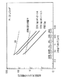
図236は、横軸に設計ルール、縦軸にFRAMのビット線容量とセル1個当りの残留分極量を示している。ここで、ビット線容量は512 WL/BLを仮定しており、微細化(設計ルールの縮小)により、僅かに減少していく。従来必要分極量Prの線は、読み出し信号:Vsを110mVと仮定して、Vs=Pr/Cbの式から、1セル当りに最低限必要な分極量Prを示している。ビット線容量Cbの低下に比例して、微細化に伴い減少しているが、緩やかな減少である。
【0016】
これに対して、強誘電体材料の残留分極量を20μC/cm2 と仮定した場合の、設計ルールでの平面キャパシタで実現した場合の得られる残留分極量を平面Capの線に示し、立体キャパシタで、底辺と高さのアスペクト比ARを1〜0.7に取った場合の得られる残留分極量を立体Cap(AR=1〜0.7)に示し、立体キャパシタで、底辺と高さのアスペクト比を2〜1.4に取った場合の得られる残留分極量を立体Cap(AR=2〜1.4)に示す。ここで、強誘電体キャパシタの底辺の面積を3F2 と仮定している(Fは設計ルール)。
【0017】
このように、実際得られる1セル当りの残留分極量は、設計ルールの2乗にほぼ比例して低下するため、設計ルール縮小に伴い急激に減少する。この図は、強誘電体キャパシタを平面で形成した場合、0.2μmルールの256MbFRAMで限界が来ることを示している。強誘電体キャパシタは、分極に異方性及び軸性を持つものが多く、立体キャパシタで十分な残留分極を得ることは難しく、いまだ立体キャパシタを実現した例が報告されていない。たとえ立体キャパシタが実現できたとしても、図236に示すように、1GbFRAM,4GbFRAMが限界点と言える。これは、従来の最大3F2 の底辺の面積を実現できるFRAMに当てはまり、セルサイズは4F2 と従来比の50%を実現できるが、キャパシタの底辺面積がF2 しか取れない、先願の発明ではさらに苦しい。
【0018】
また、従来DRAMにおいても、セル蓄積電荷量Qs=Cs× (1/2)Vdd=ε×S÷T× (1/2)Vddで定義される。ここでεは誘電率、Sはキャパシタ面積、Tはキャパシタ絶縁膜厚である。電源電圧の低下、キャパシタ面積の低下により急減にセル蓄積電荷量Qsは減少する。設計ルール縮小にも拘わらず電源電圧を緩やかに低下させた場合、Tが一定の場合、セル蓄積電荷量Qsの低下の比率は図236の強誘電体メモリと等価で、DRAMにおいては、Tを薄膜化する分だけ容量が増加するメリットがあり、さらにBST膜等で立体Capを実現できることから、1GbDRAM,4GbDRAM程度は実現できることが予測されている。
【0019】
しかしながら、BST膜においても薄膜化に限界があり、膜厚10nm程度(酸化膜厚換算0.1nm)で限界が生じる。これは第1に薄膜化自身の限界と、第2に薄膜化により、容量のバイアス電圧依存性が顕著になるためである。具体的に言うと、薄膜化するとより低電圧では容量が大きくなるが、動作バイアス電圧では容量があまり増加ないためである。DRAMセルデータ読み出しでは、動作点が1/Vddから読み出し信号電位Vsまでの間の容量が有効であり、薄膜化でVs以下の部分の容量が増加してもメリットが無いためである。このように、従来DRAMにおいても1Gb〜4GbDRAMが限界点である。
【0020】
無理をしてアスペクト比を非常に大ききすればそれ以上も実現できるが、コスト増,製造の困難さ等から考えて現実的であることが分かる。たとえBSTの替わりにPZTを用いても下限はそれほど低下しない。基本的に高誘電体材料や、強誘電体材料は同じ材料グループで、原子が移動することにより、強誘電体性を持ったり、誘電率が増加するわけであり、原子の移動には限界があると言うわけである。よって、高誘電体であっても、薄膜化して、最大分極化させると限界は、強誘電体の場合と同じになるわけである。
【0021】
また、従来のEEPROM等においても、10年間のデータリテンションを実現するには、蓄積電荷が酸化膜を通して抜けないためには8nm程度の酸化膜が必要であり、微細化に限界がある。EEPROMにおいても、多値技術を用いたとしても1Gbフラッシュメモリが限界点である。
【0022】
また、従来上記FRAMの問題点に対して、図237に示すような、自己増幅機能をもつメモリセルが各種提案されている。図237においては、各種(a)(b)(c)(d)の4種類の自己増幅機能を持つメモリセルに対して、4種類の問題が、問題であるか無いかと、セルサイズの比較が示してある。
【0023】
図237の(a)のメモリセルは、1トランジスタ形のMFSFET形或いは、MF(M)ISFET形のトランジスタを示している。MFSFET形はゲート絶縁膜に強誘電体膜を用いるトランジスタであり、格子定数が強誘電体膜とSi基板と異なるため製造が極めて困難である。MFISFET形は、ゲート絶縁膜に強誘電体膜を用い、Si基板との界面に常誘電体のバッファ膜を形成したトランジスタである。MFMISFET形は、ゲート絶縁膜に強誘電体膜を用い、Si基板との界面には、導体と常誘電体のバッファ膜を形成したトランジスタである。この場合でも製造は難しい上に、カップリング比の問題、リークの問題、誤書き込み等、実用化する上での本質的問題が山積みである。
【0024】
カップリング比の問題は、通常強誘電体膜の誘電率は、常誘電体膜の誘電率に比べて非常に大きいため、図237の右上図の等価回路に示すように、いくら常誘電体側を薄膜化しても、強誘電体膜側の容量が常誘電体側の容量より大きくなってしまい、データ書き込みのためゲートに電圧を印加しても、容量の小さい常誘電体側に書き込み電圧の殆どが印加されてしまい。結果として、書き込みに対して、従来の低電圧動作が可能なFRAMに比べて、7V〜15Vと高電圧を印加する必要が生じる。
【0025】
リークの問題は、これは致命的な問題点である。例えば、MFMISFETのゲートに電圧を印加して、強誘電体膜を分極反転させ、その後、ゲートを0Vに戻したあとのトランジスタの様子を図237の右下図に示す。強誘電体膜の分極反転によりゲート側には正の電荷が集められ、強誘電体膜と常誘電体膜の間の導電体の強誘電体膜側には、負の電荷が集められる。すると、導電体内部の電荷保存則により、あまった正の電荷がいかにも単独で導電体内部に存在しているかのようになる。この正の電荷により、常誘電体膜を介してチャネル側に負の電荷が誘起される。この負の電荷の誘起,非誘起により、トランジスタのしきい値電圧が変化して、非破壊読み出しメモリセルとして機能するわけである。
【0026】
理想的にはこれで良いのであるが、実際は導電体内部の正の電荷により導電体内部ノードの電位が上がり、導電体−ゲート間,導電体−チャネル間には電界が発生する。これにより、電子が強誘電体膜或いは常誘電体膜のどちらからでも、これを通して導電体に入り込んでしまうと、セル情報が破壊される問題が存在する。このセルデータの保存(データリテンション)は不揮発性メモリでは10年保持せねばならず、8nmのゲート酸化膜でもやっとなのに、バリアハイトの小さい強誘電体膜や、高誘電体膜では殆ど10年保証は困難と言える。今までの実測でも室温で数10秒となっており、とても高温10年は難しい。
【0027】
誤書き込みの問題は、選択セルにデータを書き込む場合、どうしても非選択セルに接続されるビット線の電位も振幅せざるをえない。このときの方式にもよるが、選択セルの少なくとも1/3〜1/2の電位が非選択セルのドレイン端子に印加してしまい誤書き込みを生じる。フラッシュメモリでも同様な問題があるが、フラッシュメモリの場合、印加電圧に対して指数関数的にF−Nトンネリング,ホットキャリアによる電流が変化するため、あまり問題ないが、印加電圧にリニアで分極反転する強誘電体形トランジスタでは深刻な問題である。
【0028】
この図237(a)のメモリセルは理論的には4F2 サイズが実現できるが、データ書き込み時にウェル電位をコントロールする必要があり、実際的には、ビット線とウェルを接続するため、4F2 より大きくなってしまう。現在6F2 のセルまでは提案されている。
【0029】
図237の(b)の回路は、(a)の強誘電体形トランジスタに選択トランジスタを介してビット線に接続した2トランジスタ型のメモリセルで、カップリング比問題,リーク問題,製造容易性,誤書き込み等の問題の内、非選択セルの選択トランジスタをOFFしておくことにより誤書き込みの問題を解決できる。しかしながら、カップリング比問題,リーク問題,製造容易性の問題は残る上、セル面積が8F2 以上と、従来FRAMと同等にまで大きくなってしまう。
【0030】
図237の(c)の回路は、リーク問題,製造容易性の問題を解決するため、強誘電体FETを用いずに、通常のトランジスタと強誘電体キャパシタを用いて構成している。トランジスタとして、書き込み用トランジスタと増幅読み出し用トランジスタを備えている。書き込みトランジスタをONして、PL−BL間に電圧を印加して分極反転させ、書き込みトランジスタをOFFして、書き込みを終了する。読み出しは、PLを駆動して、分極反転させ、“1”,“0”データにより読み出しトランジスタのゲート電圧が異なることを利用して、これをトランジスタで増幅してビット線に読み出す。しかしながら、この構成でも、強誘電体キャパシタ容量がゲート容量に比べて大きいため、カップリング比の問題が残る上に、セルサイズが12F2 以上と従来FRAMより大きくなってしまう。
【0031】
図237(d)の回路は、(c)の回路にさらに、常誘電体キャパシタを接続した場合を示し、この負荷容量により分極反転読み出しが容易になり、問題無い動作が期待できる。しかし、強誘電体キャパシタと同程度の容量或いはさらに大きな容量の常誘電体キャパシタが必要であり、16F2 以上、さらに大きなセル面積が必要になり、コスト的に実用化は困難と言える。
【0032】
このように従来の自己増幅機能をもつメモリセルにおいては、正常動作と高密度の両立は極めて困難な問題点があった。なお、この自己増幅機能を持つセルはDRAMにも適用できるが、この場合も最低2トランジスタ+1キャパシタ構成が必要で、従来DRAMより大きくなる問題点を抱えていた。
【0033】
【発明が解決しようとする課題】
以上述べたように、従来FRAMはもちろん先願においても、高密度化してメモリセルの1個1個の強誘電体キャパシタ面積が縮小した場合、残留分極量は薄膜化しても増加しないため、メモリセル1個1個当りの強誘電体キャパシタの分極量が減少してしまい、結果として読み出し信号電圧が低下して、大容量化,高密度化が困難になる大きな問題点を抱えていた。これにより、FRAMにおいては、平面キャパシタで256MbFRAMが限界点、立体キャパシタでも1Gb〜4GbFRAMが限界点となる。
【0034】
この問題は、絶縁膜の薄膜化に限界を持つDRAM等でも同様であり、DRAMにおいても1Gb〜4GbDRAMが限界点となる。また、他のフラッシュメモリでも酸化膜の薄膜化に限界があり、1Gbフラッシュメモリが限界である。つまり、従来のデータの読み書きができる半導体メモリにおいては、どれを取っても1Gb〜4Gbで限界を迎える問題点があった。
【0035】
一方、自己増幅機能を持つ従来の強誘電体メモリにおいても、カップリング比問題,リーク問題,製造容易性,誤書き込み等の本質的な問題点を抱えており、これらを解決するには、セル面積が16F2 以上と非常に大ききなる問題点を抱えていた。
【0036】
本発明は、上記事情を考慮してなされたもので、その目的とするところは、不揮発性の強誘電体メモリにおいて、高密度化してセルの強誘電体キャパシタ面積が縮小し、メモリセルの強誘電体キャパシタの分極量が減少しても、セルサイズやチップサイズの増大を抑えつつ、さらにソフトエラーを抑えつつ、十分な読み出し信号電圧を確保して、安定なメモリ動作を可能にする半導体記憶装置を提供することにある。
【0037】
また本発明の他の目的は、高密度化,製造の容易化,高速ランダムアクセル機能を保ちつつ、上記効果を実現する半導体記憶装置を提供することにある。
【0038】
また本発明のさらに他の目的は、ダイナミック型半導体メモリにおいても、高密度化してメモリセルの強誘電体キャパシタの分極量が減少しても、セルサイズ,チップサイズの増大を抑えつつ、さらにデータリテンションは向上しないが、ソフトエラーを抑えつつ、十分な読み出し信号電圧を確保して、安定なメモリ動作を可能にする半導体記憶装置を提供することにある。
【0039】
【課題を解決するための手段】
(構成)
上記課題を解決するために本発明は、次のような構成を採用している。
【0040】
即ち、本発明の半導体装置は、第1のトランジスタと、前記第1のトランジスタのソース端子に一端を接続しドレイン端子に他端を接続した第1の強誘電体キャパシタと、からメモリセルを構成し、前記メモリセルを複数個直列接続したブロックユニットと、前記ブロックユニットの一端を入力として出力をビット線に接続した増幅回路と、からセルブロックを構成し、前記セルブロックを複数配設して、メモリセルアレイを構成したことを特徴とする。
また、本発明の半導体装置は、第1のトランジスタと、前記第1のトランジスタのソース端子に一端を接続しドレイン端子に他端を接続した第1の強誘電体キャパシタと、からメモリセルを構成し、前記メモリセルを複数個直列接続したブロックユニットと、ゲート端子を前記ブロックユニットの一端に接続しドレイン端子をビット線に接続した第2のトランジスタとから、セルブロックを構成し、前記セルブロックを複数配設して、メモリセルアレイを構成したことを特徴とする。
また、本発明の半導体装置は、第1のトランジスタと、前記第1のトランジスタのソース端子に一端を接続しドレイン端子に他端を接続した第1の強誘電体キャパシタと、からメモリセルを構成し、前記メモリセルを複数個直列接続したブロックユニットと、ゲート端子を前記ブロックユニットの一端に接続しドレイン端子をビット線に接続した第2のトランジスタと、ソース端子を前記ブロックユニットの前記一端に接続しドレイン端子を前 記ビット線に接続した第3のトランジスタと、からセルブロックを構成し、前記セルブロックを複数配設して、メモリセルアレイを構成したことを特徴とする。
また、本発明の半導体装置は、第1のトランジスタと、前記第1のトランジスタのソース端子に一端を接続しドレイン端子に他端を接続した第1の強誘電体キャパシタと、からメモリセルを構成し、前記メモリセルを複数個直列接続した第1,第2のブロックユニットと、ゲート端子を前記第1のブロックユニットの一端に接続しドレイン端子を第2のビット線に接続した第2のトランジスタと、ソース端子を前記第1のブロックユニットの前記一端に接続しドレイン端子を第1のビット線に接続した第3のトランジスタと、ゲート端子を前記第2のブロックユニットの一端に接続しドレイン端子を前記第1のビット線に接続した第4のトランジスタと、ソース端子を前記第2のブロックユニットの一端に接続しドレイン端子を前記第2のビット線に接続した第5のトランジスタと、からセルブロックを構成し、前記セルブロックを複数配設して、メモリセルアレイを構成したことを特徴とする。
また、本発明の半導体装置は、第1のトランジスタと、前記第1のトランジスタのソース端子に一端を接続しドレイン端子に他端を接続した第1の強誘電体キャパシタと、からメモリセルを構成し、前記メモリセルを複数個直列接続した第1,第2,第3,第4のブロックユニットと、ゲート端子を前記第1,第3のブロックユニットの各一端を接続した端子に接続しドレイン端子を第2のビット線に接続した第2のトランジスタと、ソース端子を前記第1,第3のブロックユニットの各一端を接続した端子に接続しドレイン端子を第1のビット線に接続した第3のトランジスタと、ゲート端子を前記第2,第4のブロックユニットの各一端を接続した端子に接続しドレイン端子を前記第1のビット線に接続した第4のトランジスタと、ソース端子を前記第2,第4のブロックユニットの各一端を接続した端子に接続しドレイン端子を前記第2のビット線に接続した第5のトランジスタと、からセルブロックを構成し、前記セルブロックを複数配設して、メモリセルアレイを構成したことを特徴とする。
また、本発明の半導体装置は、第1のトランジスタと、前記第1のトランジスタのソース端子に一端を接続しドレイン端子に他端を接続した第1の強誘電体キャパシタと、からメモリセルを構成し、前記メモリセルを複数個直列接続したブロックユニットと少なくとも1個以上の選択トランジスタを直列接続したものから、セルブロックを構成し、サブビット線と、前記サブビット線に前記選択トランジスタが接続された側の一端を接続した複数の前記セルブロックと、前記サブビット線を入力とし出力をビット線に接続する増幅回路と、からセルセグメントを構成し、複数の前記ビット線と、複数の前記ビット線の各々に接続される複数の前記セルセグメントと、からメモリセルアレイを構成したことを特徴とする。
また、本発明の半導体装置は、第1のトランジスタと、前記第1のトランジスタのソース端子に一端を接続しドレイン端子に他端を接続した第1の強誘電体キャパシタと、からメモリセルを構成し、前記メモリセルを複数個直列接続したブロックユニットと少なくとも1個以上の選択トランジスタを直列接続したものから、セルブロックを構成し、サブビット線と、前記サブビット線に前記選択トランジスタが接続された側の一端を接続した複数の前記セルブロックと、前記サブビット線をゲート端子に接続し、ドレイン端子をビット線に接続する第2のトランジスタと、からセルセグメントを構成し、複数の前記ビット線と、複数の前記ビット線の各々に接続される複数の前記セルセグメントと、からメモリセルアレイを構成したことを特徴とする。
また、本発明の半導体装置は、第1のトランジスタと、前記第1のトランジスタのソース端子に一端を接続しドレイン端子に他端を接続した第1の強誘電体キャパシタと、からメモリセルを構成し、前記メモリセルを複数個直列接続したブロックユニットと少なくとも1個以上の選択トランジスタを直列接続したものから、セルブロックを構成し、第1,第2のサブビット線と、前記第1,第2のサブビット線の各々に前記選択トランジスタが接続された側の一端を接続する複数の前記セルブロックと、前記第1のサブビット線をゲート端子に接続し、第2のビット線をドレイン端子に接続した第2のトランジスタと、前 記第1のサブビット線をソース端子に、ドレイン端子を第1のビット線に接続した第3のトランジスタと、前記第2のサブビット線をゲート端子に接続し、前記第1のビット線をドレイン端子に接続した第4のトランジスタと、前記第2のサブビット線をソース端子に、ドレイン端子を前記第2のビット線に接続した、第5のトランジスタと、からセルセグメントを構成し、複数の前記第1,第2のビット線と、複数の前記第1,第2のビット線の各々に接続される複数の前記セルセグメントと、からメモリセルアレイを構成したことを特徴とする。
また、本発明の半導体装置は、第1のトランジスタと、前記第1のトランジスタのソース端子に一端を接続しドレイン端子に他端を接続した第1の強誘電体キャパシタと、からメモリセルを構成し、前記メモリセルを複数個直列接続したブロックユニットと少なくとも1個以上の選択トランジスタを直列接続したものから、セルブロックを構成し、第1,第2のサブビット線と、前記第1,第2のサブビット線の各々に前記選択トランジスタが接続された側の一端を接続する複数の前記セルブロックと、前記第1のサブビット線をゲート端子に接続し、第1のビット線をドレイン端子に接続した第2のトランジスタと、前記第1のサブビット線をソース端子に、ドレイン端子を前記第1のビット線に接続した第3のトランジスタと、前記第2のサブビット線をゲート端子に接続し、第2のビット線をドレイン端子に接続した第4のトランジスタと、前記第2のサブビット線をソース端子に、ドレイン端子を前記第2のビット線に接続した第5のトランジスタと、からセルセグメントを構成し、複数の前記第1,第2のビット線と、複数の前記第1,第2のビット線の各々に接続される複数の前記セルセグメントと、からメモリセルアレイを構成したことを特徴とする。
また、本発明の半導体装置は、第1のトランジスタと、前記第1のトランジスタのソース端子を一端に接続しプレート線を他端に接続した第1の強誘電体キャパシタと、からメモリセルを構成し、サブビット線と、前記サブビット線に前記第1のトランジスタのドレイン端子を接続した複数の前記メモリセルと、前記サブビット線を入力とし出力をビット線に接続する増幅回路と、からセルセグメントを構成し、複数の前記ビット線と、複数の前記ビット線の各々に接続される複数の前記セルセグメントと、からメモリセルアレイを構成したことを特徴とする。
また、本発明の半導体装置は、第1のトランジスタと、前記第1のトランジスタのソース端子を一端に接続しプレート線を他端に接続した第1の強誘電体キャパシタと、からメモリセルを構成し、サブビット線と、前記サブビット線に前記第1のトランジスタのドレイン端子を接続した複数の前記メモリセルと、前記サブビット線をゲート端子に接続し、ドレイン端子をビット線に接続する第2のトランジスタと、からセルセグメントを構成し、複数の前記ビット線と、複数の前記ビット線の各々に接続される複数の前記セルセグメントと、からメモリセルアレイを構成したことを特徴とする。
また、本発明の半導体装置は、第1のトランジスタと、前記第1のトランジスタのソース端子を一端に接続しプレート線を他端に接続した第1の強誘電体キャパシタと、からメモリセルを構成し、第1,第2のサブビット線と、前記第1,第2のサブビット線の各々に前記第1のトランジスタのドレイン端子を接続した複数の前記メモリセルと、前記第1のサブビット線をゲート端子に接続し、第2のビット線をドレイン端子に接続した第2のトランジスタと、前記第1のサブビット線をソース端子に、ドレイン端子を第1のビット線に接続した第3のトランジスタと、前記第2のサブビット線をゲート端子に接続し、前記第1のビット線をドレイン端子に接続した第4のトランジスタと、前記第2のサブビット線をソース端子に、ドレイン端子を前記第2のビット線に接続した第5のトランジスタと、からセルセグメントを構成し、複数の前記第1,第2のビット線と、複数の前記第1,第2のビット線の各々に接続される複数の前記セルセグメントと、からメモリセルアレイを構成したことを特徴とする。
また、本発明の半導体装置は、第1のトランジスタと、前記第1のトランジスタのソース端子を一端に接続しプレート線を他端に接続した第1の強誘電体キャパシタと、からメモリセルを構成し、第1,第2のサブビット線と、前記第1,第2のサブビット線の各々 に前記第1のトランジスタのドレイン端子を接続した複数の前記メモリセルと、前記第1のサブビット線をゲート端子に接続し、第1のビット線をドレイン端子に接続した第2のトランジスタと、前記第1のサブビット線をソース端子に、ドレイン端子を前記第1のビット線に接続した第3のトランジスタと、前記第2のサブビット線をゲート端子に接続し、第2のビット線をドレイン端子に接続した第4のトランジスタと、前記第2のサブビット線をソース端子に、ドレイン端子を前記第2のビット線に接続した第5のトランジスタと、からセルセグメントを構成し、複数の前記第1,第2のビット線と、複数の前記第1,第2のビット線の各々に接続される複数の前記セルセグメントと、からメモリセルアレイを構成したことを特徴とする。
(作用)
本発明(請求項1〜4)によれば、強誘電体キャパシタとセルトランジスタを並列接続して、1セルとしてこれを複数直列接続して、ブロックユニットを構成することにより、4F2 サイズの高密度のセルを実現しつつ、平面トランジスタで製造の容易化を実現し、さらに高速なランダムアクセス機能を有することが可能となる。さらに、このブロックユニットの一端を増幅トランジスタのゲートに入力して、ドレイン端子をビット線に接続することにより、メモリセルの分極反転読み出しにより、ブロックユニットの一端に読み出されたデータを増幅して、ビット線に伝えることができる。
【0041】
高密度化して、セルの強誘電体キャパシタ面積が縮小し、メモリセルの強誘電体キャパシタの分極量が減少しても、それに対応してブロックユニットの一端の負荷容量を小さくでき、この効果により、ブロックユニットの一端に読み出される電荷は小さくなるが、十分大きな読み出し信号電圧を確保できる。この信号を前記増幅トランジスタを用いて、このトランジスタのドレイン端子をビット線に接続することにより、負荷容量の大きなビット線の電位を放電してやれば、正常にメモリ動作が実現できる。増幅後、書き込みトランジスタをONしてやることにより、データの再書き込みが容易に実現できる。
【0042】
従来の自己増幅機能のあるメモリセルでは安定動作,正常動作させるには、メモリセル面積が非常に大きくなる問題点が有ったが、本発明によれば、1個のブロックユニット内のセル数を増加するほど、複数のメモリセルで、前記増幅トランジスタと書き込みトランジスタを共用でき、セルサイズのオーバヘッドを小さなものにできる。さらに、ビット線につながるセルブロック数をいくら多くしても、基本的に時間さえ許せばビット線に読み出す信号を確保できるため、センスアンプ回路数を大幅に低減できる効果があり、チップサイズの増大を抑え、設計によってはチップサイズを先願より小さくできる。
【0043】
ブロックユニットの一端に読み出される信号は大きいままだが、その反面電荷が小さくなり、この読み出し時のソフトエラーが問題となる。従来の自己増幅機能を有するメモリセルでは、この問題は致命的であるが、本発明においては、設計ルールが緩く、ソフトエラーが厳しい状況では、ブロックユニットの一端に大きな負荷容量を追加してやれば、この問題はクリアできる。この負荷容量も複数のセルで共有できるため、オーバヘッドを抑えることができるし、設計ルールが小さくなるに従って、ソフトエラーレートが下がるに従って小さくすることができる。
【0044】
このように本発明により、製造容易な平面強誘電体キャパシタでも高密度の強誘電体メモリ動作が実現できる。
【0045】
本発明(請求項5)によれば、請求項1〜4の効果に加え、第1に、2つのブロックユニットで増幅トランジスタ(第2,4のトランジスタ)と書き込みトランジスタ(第3,5のトランジスタ)を共有するため、さらに1セル当りのオーバヘッドを小さくできる。第2に、選択したブロックユニット内の選択したメモリセルの位置により、ブロックユニットの一端の負荷容量が大きく変化する問題が請求項1〜4にはあり、安定動作には余分な負荷容量を追加する必要性が生じるが、本発明によれば、一方のブロックユニット選択時に他方のブロックユニットの内部容量が負荷容量になるため、請求項1〜4よりも安定な動作が可能になるし、余分な負荷容量を追加する必要性が必ずしも生じない。これにより、安定動作とセルサイズのオーバヘッドを防げる。
【0046】
第3に、ブロックユニットの一端に読み出される信号は大きいままだが、その反面電荷が小さくなり、ソフトエラー増加する問題に対して設計ルールが緩く、ソフトエラーが厳しい状況では、ブロックユニット内の直列セル数を多くすれば、自動的に負荷容量を確保できる。さらに、設計ルールが小さくなるに従ってセル分極量が2乗で減り、読み出し電荷が減り、ソフトエラーレートが下がるに従って直列接続数を減らせば、ブロックユニットの一端に読み出される信号を確保できる。このように、ソフトエラーの下限考慮しつつ直列セル数を選べば、ソフトエラーの問題は回避できる。
【0047】
このように本発明により、製造容易な平面強誘電体キャパシタでも高密度の強誘電体メモリ動作が実現できる。
【0048】
本発明(請求項19〜22)によれば、強誘電体キャパシタとセルトランジスタを並列接続して、1セルとしてこれを複数直列接続して、さらに選択トランジスタを介して、サブビット線に接続してセルブロックを構成することにより、4F2 サイズの高密度のセルを実現しつつ、平面トランジスタで製造の容易化を実現し、さらに高速なランダムアクセス機能を有することが可能となる。さらに、サブビット線と、これに接続される複数セルブロックと、サブビット線をゲートに入力して、ドレイン端子をビット線に接続する増幅トランジスタを、含む素子でセルセグメントを構成することにより、メモリセルの分極反転読み出しにより、サブビット線に読み出されたデータを増幅して、ビット線に伝えることができる。
【0049】
高密度化して、セルの強誘電体キャパシタ面積が縮小し、メモリセルの強誘電体キャパシタの分極量が減少しても、それに対応して1個のセルセグメント内のセルブロック数を減少させてやれば、サブビット線に読み出される電荷は小さくなるが、十分大きな読み出し信号電圧を確保できる。この信号電圧を前記増幅トランジスタを用いて、このトランジスタのドレイン端子をビット線に接続することにより、負荷容量の大きなビット線の電位を放電してやれば、正常にメモリ動作が実現できる。増幅後、書き込みトランジスタをONしてやることにより、ビット線からサブビット線へ、さらにメモリセルへのデータの再書き込みが容易に実現できる。
【0050】
従来の自己増幅機能のあるメモリセルでは安定動作,正常動作させるには、メモリセル面積が非常に大きくなる問題点が有ったが、本発明によれば、1個のセルセグメント内のセルブロック数を増加するほど、複数のメモリセルで、前記増幅トランジスタと書き込みトランジスタを共用でき、セルサイズのオーバヘッドを小さなものにできる。さらに、ビット線につながるセルブロック数をいくら多くしても、基本的に時間さえ許せばビット線に読み出す信号を確保できるため、センスアンプ回路数を大幅に低減できる効果があり、チップサイズの増大を抑えることができる。
【0051】
ソフトエラー増加する問題に対して本発明に於いては、設計ルールが緩く、ソフトエラーが厳しい状況では、セルセグメント内のセルブロック数を多くすれば、自動的に負荷容量を確保できるし、設計ルールが小さくなるに従ってセル分極量が2乗で減り、読み出し電荷が減り、ソフトエラーレートが下がるに従ってセルブロック数を減らせば、サブビット線に読み出される信号を確保できる。このように、ソフトエラーの下限考慮しつつセルセグメント内のセル数を選べば、ソフトエラーの問題は回避できる。
【0052】
このように本発明により、製造容易な平面強誘電体キャパシタでも高密度の強誘電体メモリ動作が実現できる。
【0053】
本発明(請求項30〜33)によれば、従来の強誘電体メモリと同じように、強誘電体キャパシタとセルトランジスタを直列接続して1セルを構成し、さらに、サブビット線と、これに接続される複数のメモリセルと、サブビット線をゲートに入力して、ドレイン端子をビット線に接続する増幅トランジスタを、含む素子でセルセグメントを構成することにより、メモリセルの分極反転読み出しにより、サブビット線に読み出されたデータを増幅して、ビット線に伝えることができる。
【0054】
高密度化して、セルの強誘電体キャパシタ面積が縮小し、メモリセルの強誘電体キャパシタの分極量が減少しても、それに対応して1個のセルセグメント内のセル数を減少させてやれば、サブビット線に読み出される、電荷は小さくなるが、十分大きな読み出し信号電圧を確保できる。この信号を前記増幅トランジスタを用いて、このトランジスタのドレイン端子をビット線に接続することにより、負荷容量の大きなビット線の電位を放電してやれば、正常にメモリ動作が実現できる。増幅後、書き込みトランジスタをONしてやることにより、ビット線から、サブビット線へ、さらにメモリセルへのデータの再書き込みが容易に実現できる。
【0055】
従来の自己増幅機能のあるメモリセルでは、安定動作,正常動作させるには、メモリセル面積が非常に大きくなる問題点が有ったが、本発明によれば、1個のセルセグメント内のセル数を増加するほど、複数のメモリセルで、前記増幅トランジスタと書き込みトランジスタを共用でき、セルサイズのオーバヘッドを小さなものにできる。さらに、ビット線につながるセルブロック数をいくら多くしても、基本的に時間さえ許せばビット線に読み出す信号を確保できるため、センスアンプ回路数を大幅に低減できる効果があり、チップサイズの増大を抑えることができる。
【0056】
ソフトエラー増加する問題に対して本発明においては、設計ルールが緩くソフトエラーが厳しい状況では、セルセグメント内のセル数を多くすれば、自動的に負荷容量を確保できるし、設計ルールが小さくなるに従ってセル分極量が2乗で減り、読み出し電荷が減り、ソフトエラーレートが下がるに従ってセル数を減らせば、サブビット線に読み出される信号を確保できる。このように、ソフトエラーの下限考慮しつつセルセグメント内のセル数を選べば、ソフトエラーの問題は回避できる。
【0057】
このように本発明により、製造容易な平面強誘電体キャパシタでも高密度の強誘電体メモリ動作が実現できる。
【0058】
【発明の実施の形態】
まず、発明の実施形態を説明する前に、本発明者らが既に提案した先願について説明する。
【0059】
(従来の技術)の項で説明した第1,第2の大きな問題点に対して本発明者らは、特願平9−153137号において、不揮発性の強誘電体メモリで、(1) 小さい4F2 サイズのメモリセル、(2) 製造が容易な平面トランジスタ、(3) 汎用性のあるランダムアクセス機能、の3点が両立でき、しかもPL電位固定で高速化を保ちつつ、スタンドバイ中でもデータ保持が可能でリフレッシュ動作を不要とする半導体記憶装置を既に提供している。さらに、特願平9−346404号においては、PL駆動方式であっても、高速動作が実現できる半導体記憶装置を既に提案している。
【0060】
先願の概要を簡単に述べる。図231に、特願平9−153137号の発明のメモリセルの構成回路とセル構造、図232にその動作例を示す。図231(a)に等価回路図、(b)に素子構造断面図を示すように、1個のメモリセルは、セルトランジスタと強誘電体キャパシタの並列接続で構成され、1つのメモリセルブロックは、この並列接続のメモリセルを複数直列接続して、一端はブロック選択トランジスタを介してビット線に接続され、他端はプレートに接続される。この構成により、平面トランジスタを用いて、4F2 サイズのメモリセルが実現できる。
【0061】
図232(a)に示すように、スタンドバイ時には、全てのメモリセルトランジスタをONにしておき、ブロック選択トランジスタをOFFにしておく。こうすることにより、強誘電体キャパシタの両端は、ONしているセルトランジスタにより電気的にショートされるため、両端の電位差は発生しない。よって、“1”の分極データは、図232(a)のヒステリス曲線の“1”の点、“0”の分極データは、ヒステリス曲線の“0”の点に安定に保持される。これにより、スタンドバイ時、pn接合リーク等の各種リーク電流があろうと、プレートの駆動方式が、0V〜Vdd駆動方式であろうと、(1/2)Vdd固定方式であろうと、セルデータは安全に保持される。
【0062】
図232(b)に示すように、アクティブ時は、読み出したい強誘電体キャパシタに並列に接続されるメモリセルトランジスタのみOFFにして、ブロック選択トランジスタをONにする。この時、PLとBL間の電位差が、OFFしたメモリセルトランジスタに並列接続した強誘電体キャパシタの両端にのみ印加され、強誘電体キャパシタの分極情報がビット線に読み出される。よって、セルを直列接続しても、任意のワード線を選択することにより、任意の強誘電体キャパシタのセル情報が読み出され、完全なランダムアクセスが実現できるわけである。これにより、図231に示すセルブロックにより、オープンBL構成が実現できる。
【0063】
図231に示すセルブロックを2個対にして、各々をビット線対(/BL,BL)のどちらかに接続して、2個のセルブロックで同じワード線に接続される2個のメモリセルを組みにして、2トランジスタ/2強誘電体キャパシタ(=2T/2C)で1ビットを記憶すれば、フォールデッドBL方式が実現できる。また、図233に示すように、ブロック選択トランジスタを2個直列接続して、一方をデプレッション型トランジスタにし、ブロック選択トランジスタ(BS0,BS1)のどちらか一方をHighにすると、2つのセルブロックの一方のデータしかビット線に読み出されず、ビット線対の他方をリファレンスビット線にすれば、これもフォールデッドBL構成が実現できる。この場合、プレート電極は、 (1/2)Vddに固定される。図233の下図はフォールデッドBL方式の動作例に示す。
【0064】
また、特願平9−346404号においては、PL駆動方式であっても、高速動作及び非選択メモリセルへのノイズを無くすることができる半導体記憶装置を既に提供している。これを図234に示す。図233と比べて、PL線を2種類に分割している。例えば、下図の動作例に示すように、/BLに接続するセルを選択する場合、PL(/BL)のみを0VからVddに駆動して、PL(BL)は0V固定のままである。これにより、図233において同様に/BLに接続するセルを選択した場合で、PLを駆動した場合BLに接続され、選択ワード線をOFFした時に同じ選択ワード線に接続され、BL側に接続されるセルに、PL駆動により、セルトランジスタがOFFしているため、セルの強誘電体キャパシタに不要な電圧が印加さえるのを防ぐことができる。
【0065】
しかしながら、上記した先願においても先に説明したように、高密度化してメモリセルの1個1個の強誘電体キャパシタ面積が縮小した場合、メモリセル1個1個当りの強誘電体キャパシタの分極量が減少してしまい、結果として読み出し信号電圧が低下して、大容量化,高密度化が困難になる大きな問題点を抱えている。
【0066】
以下、本発明の詳細を図示の実施形態によって説明する。
【0067】
(第1の実施形態)
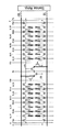
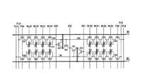
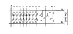
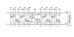
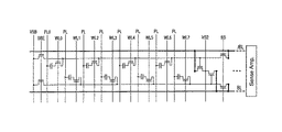
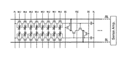
図1は、本発明の第1の実施形態に係わる半導体記憶装置を示す回路構成図であり、特に強誘電体メモリのセルブロック構成を示している。本実施形態は、先願である特願平9−153137号及び特願平9−346404号と同様に、1個のメモリセルは、セルトランジスタと強誘電体キャパシタの並列接続で構成され、セルトランジスタのゲートは、ワード線WLA0〜WLA3,WLB0〜WLB3に接続される。
【0068】
1つのメモリセルのブロックユニットは、4個の直列接続されたメモリセルで構成されている。ここまでは先願と同じである。本実施形態においては、1個のセルブロックは4個のブロックユニットによって構成され、左上のブロックユニットと右上のブロックユニットはサブビット線(/SBL)に接続され、左下のブロックユニットと右上のブロックユニットはサブビット線(SBL)に接続される。左上のブロックユニットはトランジスタQ1を介してプレート線/PLAに接続され、左下のブロックユニットはトランジスタQ2を介してPLAに接続され、右上のブロックユニットはトランジスタQ3を介してプレート線/PLBに接続され、右下のブロックユニットはトランジスタQ4を介してPLBに接続されている。
【0069】
トランジスタQ5は、サブビット線/SBLをゲート入力として、ソースをVSE電位に接続して、ドレインをビット線BLに接続しており、このトランジスタQ5を用いて/SBLの電位を増幅してビット線BLに伝える。トランジスタQ7は逆に、再書き込み時或いは書き込み時、ブロック書き込み選択信号BS0をHighにして、ビット線/BLからの書き込み電位を、トランジスタQ7を介してサブビット線/SBLに伝え、セルにデータを再書き込みするのに用いている。
【0070】
トランジスタQ6は、サブビット線(SBL)をゲート入力として、ソースをVSE電位に接続して、ドレインをビット線/BLに接続しており、このトランジスタQ6を用いてSBLの電位を増幅してビット線/BLに伝える。トランジスタQ8は逆に、再書き込み時或いは書き込み時、ブロック書き込み選択信号BS1をHighにして、ビット線BLからの書き込み電位を、トランジスタQ8を介してサブビット線SBLに伝え、セルにデータを再書き込みするのに用いている。
【0071】
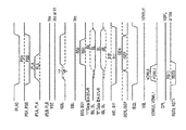
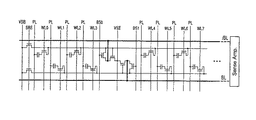
図2は、図1の具体的な動作例を示す信号波形図であり、特にセルトランジスタQ9と強誘電体キャパシタCF1で構成されるメモリセルのデータを読み出し,再書き込みする場合の動作例を示している。
【0072】
まず、スタンドバイ時は、全てのワード線WLA0〜3,WLB0〜3は昇圧電位Vpp、全てのプレート/PLA,PLA,/PLB,PLBは0V、プレート選択信号PSA,PLBをVppにしておくことにより、セルトランジスタは全てONしており、全てのセルの強誘電体キャパシタの両端は電気的にショートされて、さらにこの両端の電位及びサブビット線/SBL,SBLの電位は、プレート選択信号がHighのため、プレートに接続され0Vになっている。また、ブロック書き込み選択信号BS0,BS1は0Vにしておくことにより、トランジスタQ7,Q8はOFFしており、/SBL,SBLが0V、VSEが0Vのため、増幅トランジスタQ5,Q6もOFFしている。よって、ビット線/BL,BLとサブビット線/SBL,SBLは完全に分離されている。
【0073】
ビット線/BL,BLは従来FRAMにおいては、0Vにプリチャージする必要があったが、本実施形態においては、従来DRAMと同様に、(1/2)VBLHにプリチャージすることができる。ここで、 VBLH はビット線振幅のHighレベルを示す。
【0074】
動作時は、選択したセルブロックの例えば、左上のブロックユニットのメモリセル(Q9,CF1)選択時の動作を説明する。まず、選択メモリセルにつながるワード線WLA0を0Vに下げセルトランジスタQ9をOFFする。同時に、或いは前後して、右上,右下のブロックユニットとプレート/PLB,PLBを切り離すため、プレート選択信号PSBを0Vに下げトランジスタQ3,Q4をOFFする。さらに、ビット線/BL,BLを (1/2)VBLHのままフローティングにする。ここでQ1,Q2はONのままである。これにより、セルトランジスタQ9はOFF、トランジスタQ3はOFFしているため、選択したセルの強誘電体キャパシタCF1の右側の端子から/SBL、さらに右上のブロックユニットのセル内部ノードは全てつながり、かつ0Vでフローティングになる。
【0075】
次に、選択した左上のブロックユニットに接続されるプレート/PLAのみを0Vから VBLH に上げる。PLAから選択した強誘電体キャパシタの左側端子まで VBLH 電位が印加される。このとき、CF1の右側の端子から/SBL、さらに右上のブロックユニットのセル内部ノードの容量が負荷容量CLとなり、強誘電体キャパシタに“1”データが書き込んであれば、分極反転して、セルデータがサブビット線/SBL(正確には、CF1の右側の端子から/SBL、さらに、右上のブロックユニットのセル内部ノード)に読み出され/SBLの電位が0Vから2Vs+Voに上がる。
【0076】
強誘電体キャパシタに“0”データが書き込んであれば、分極反転せず、CF1の常誘電体成分容量とCLの容量比分だけサブビット線/SBLの電位が上がり、/SBLの電位はVoとなる。このとき、対を成すサブビット線SBLの電位はPLAが0Vのままなので、0Vのままである。また、VSE電位を0Vに設定しておくと、増幅トランジスタQ5のゲート電位は、“1”データ時は2Vs+Vo、“0”データ時はVo、ソース電位(=VSE)は0V、ドレイン電位(=/BL)は (1/2)VBLHとなる。
【0077】
そして、トランジスタQ5のしきい値電圧VtをVo<Vt<2Vs+Voに設計しておくと、図2に示すように、“1”データ時にトランジスタQ5はONしているため、(1/2)VBLHにプリチャージされているBLは増幅トランジスタQ5を介して、VSEに電流が流れることにより、(1/2)VBLH から電位が下がり始める。ここで、センスアンプ動作前の下がった電位を (1/2)VBLH−2Vst定義する。
【0078】
逆に、“0”データ時はトランジスタQ5はOFFしているため、 (1/2)VBLHにプリチャージされているBLは増幅トランジスタQ5を介して、VSEに電流が流れず、 (1/2)VBLHのままである。このとき、定電流駆動トランジスタを用いたダミーセル等を用いて、/BL電位を“1”データ時にBL側が下がる電位の半分の電位下げるように設定すると(即ちセンス動作前、(1/2)VBLH−Vst)、センスアンプ動作前の“1”データ時、BLは (1/2)VBLH−2Vst、/BLは (1/2)VBLH−Vstとなり、Vstの電位差が図1の右のセンスアンプに入力され、フリップフロップ型のセンスアンプで増幅され、BLは0V、/BLは VBLHとなる。また、“0”データ時、BLは (1/2)VBLH、/BLは (1/2)VBLH−Vstとなり、Vstの電位差が図1の右のセンスアンプに入力され、フリップフロップ型のセンスアンプで増幅され、BLはVBLH、/BLは0Vとなる。
【0079】
なお、上記増幅トランジスタのしきい値電圧は、Vt<Voの領域であった場合、/BLとBLの両方が増幅トランジスタがONして、/BL,BL電位が下がるわけであるが、この場合でも駆動電流に大きな違いがあり、ダミーセルの駆動電流を適切に設計すれば問題無い。また、VSEの電位は0Vでも良いし、しきい値の補正のため、ある一定の電位でも良い(即ち、VSEを0Vから上げた分見かけ上増幅トランジスタのしきい値電圧を上げることができる)。
【0080】
データの再書き込み時、サブビット線/SBLに接続されるブロック書き込み制御信号BS0のみVppに上げる。すると、0V或いは VBLH に増幅されたビット線/BLの電位が/SBLに書き込まれ、“1”データ時、/SBLは VBLH となり、“0”データ時/SBLは0Vになる。このとき、プレート電位(=選択強誘電体キャパシタの左側の端子)は VBLH のため、“0”データ時、強誘電体キャパシタには−VBLHの電圧(強誘電体キャパシタの右側の端子を正と定義)が印加され、“0”データが再書き込みされる。“1”データ時は、その後、プレート/PLAが0Vに下げられ、選択強誘電体キャパシタの左側の端子も0Vになった時、強誘電体キャパシタには VBLH の電圧(強誘電体キャパシタの右側の端子を正と定義)が印加され、“1”データが再書き込みされる。
【0081】
これら一連の動作において、SBL電位はずっと0Vのままなので、下のブロックユニットのデータは保持されたまま、安定である。例えば、外部から異なるデータを書き込む場合(Write Mode)や、データの読み出し後外部データを書き込む場合(Read Modified Write )、BS0がHighになったあと書き込めば良い。
【0082】
再書き込み終了後は、まずブロック書き込み選択信号BS0をHighから0Vに下げる。これにより、/BL側から/SBLへの干渉は無くなる。その後、WLA0を上げ、同時に或いは前後して、プレート制御信号PSAを上げると、選択されていたセルの強誘電体キャパシタは電気的にショートされ、右上,左上のブロックユニットの内部ノードと/SBLノードは0Vになる。これら動作と同時に或いは前後して、ビット線対/BL,BLを電気的にショートしてやれば、ビット線対は (1/2)VBLHになり、スタンドバイ状態に戻る。
【0083】
本実施形態においては、ビット線のプリチャージ電位を (1/2)VBLHにしているが、これができるのは、セル情報分極反転読み出すための負荷容量はサブビット線/SBL,SBLで行い、ビット線/BL,BLはセル情報分極反転読み出すための負荷容量では無いためである。このため、ビット対を電気的にショートするだけでプリチャージ電位である (1/2)VBLHが得られ、ビット線の充放電による消費電力を従来DRAM同様従来FRAMの半分に低減できるし、ビット線の充放電によるノイズを低減できる。
【0084】
以上、図1の回路図と図2の動作例で説明した本実施形態は、先願と同様に、強誘電体キャパシタとセルトランジスタを並列接続して、1セルとしてこれを複数直列接続して、ブロックユニットを構成することにより、4F2 サイズの高密度のセルを実現しつつ、平面トランジスタで製造の容易化を実現し、さらに高速なランダムアクセス機能を有することが可能となる。
【0085】
ここで、従来のFRAMにおいては、高密度化して設計ルールが縮小し、セルの強誘電体キャパシタ面積が設計ルールのほぼ2乗で縮小し、メモリセルの強誘電体キャパシタの分極量が減少するにも拘わらずビット線容量がそれほど減少しないため、読み出し信号量が減少して、動作が困難になる問題点が有った。これに対し本実施形態では、ブロックユニットの一端を増幅トランジスタのゲートに入力して、ドレイン端子をビット線に接続することにより、メモリセルの分極反転読み出しにより、ブロックユニットの一端に読み出されたデータを増幅して、ビット線に伝えることができる。
【0086】
このとき、強誘電体キャパシタが分極反転するときの負荷容量CLは、CF1の右側の端子から/SBL、さらに右上のブロックユニットのセル内部ノードの容量となり、ビット線容量に比べて大幅に小さい値を取ることができ、強誘電体キャパシタサイズが小さくなっても、/SBLに読み出される信号量、即ち“1”データ時2Vs+Vo、“0”データ時Voの差の1/2であるVsの値は、大きな値を取ることが可能になる。これを増幅トランジスタQ5で増幅するため、いくらビット線/BL,BLの容量が大きくても安定動作が可能となる。例えば、セルブロック内の容量が従来FRAMのビット線容量の1/10であれば、強誘電体キャパシタの面積を1/10程度に縮小しても動作すると言うわけである。
【0087】
これは逆に言うと本実施形態によれば、ビット線容量を増加しても、増幅トランジスタがビット線に読み出す信号を増幅するのに時間がかかるだけで、いくらでもビット線容量を増加できることになる。即ち、1本のビット線に接続されるセルブロック数をいくらでも増加できるため、従来FRAMのような、チップ面積に占めるセンスアンプ面積が15%〜20%もある問題を解決して、ビット線に接続されるセルブロック数を増加させ、センスアンプ数を減らし、センスアンプ面積のオーバヘッドを殆ど無くすることによりチップサイズを小さくする効果がある。
【0088】
本実施形態におけるセルブロック内部の負荷容量CLは、ブロックユニット内の直列セル数の増減により変更が容易である。このことは、強誘電体キャパシタサイズが大きい時は、直列セル数を増加してCLを大きくして設計し、強誘電体キャパシタサイズが小さい時は、直列セル数を減らしてCLを小さくして設計し、サブビット線に読み出される信号量を確保すれば良いことを示す。負荷容量CLが小さい場合、サブビット線に読み出される電位は確かに大きく確保できるが、総電荷量が小さいため、セルデータ読み出し時のサブビット線の拡散層に当るソフトエラーが問題となる。
【0089】
この問題に対して、上記直列セル数の調整が有効である。即ち、設計ルールが緩く、ソフトエラーが厳しい状況では、ブロックユニットの直列セル数を増加させ、負荷容量を追加してやれば、Qs=Vs×CLであり、多少Vsが減ってもQsが多くなり、より多くの反転電荷がサブビット線に読み出され、この問題はクリアできる。設計ルールが小さくなるに従って、ソフトエラーレートが下がるに従って、ソフトエラーが問題無い程度に、直列セル数を徐々に減らして、サブビット線に読み出される信号量を確保すれば良いことが分かる。
【0090】
従来の自己増幅機能のあるメモリセルではこの調整をしようとすると、図237(d)のセルに限定される上、常誘電体キャパシタ面積が非常に大ききなり、コスト的に困難である。従来の自己増幅機能のあるメモリセルと比較すると、常誘電体キャパシタの大きな図237(d)のセルと同じ安定動作,正常動作を可能にしつつ、本実施形態よれば、1個のブロックユニット内のセル数を増加するほど、複数のメモリセルで前記増幅トランジスタと書き込みトランジスタを共用でき、セルサイズのオーバヘッドを極めて小さなものにできる。
【0091】
さらに図1の回路においては、左右のブロックユニットで増幅トランジスタやブロック書き込み選択トランジスタを共有しているわけで、これらのオーバヘッドは小さい。本実施形態のセルブロック構造では、ブロックユニット内の選択したセルの位置により、CLの値が変化する問題に対して、少なくとも、選択したブロックユニットの反対側のブロックユニットの内部容量がその他の増幅トランジスタ等の容量に加算されて負荷容量になるため、選択ワード線の位置のCL値依存性は1/2以下に抑えられる。この左右ブロックユニットのサブビット線共有は、図1に示すような、プレート選択トランジスタを導入して、選択ブロックユニットと反対側のブロックユニットのプレート選択トランジスタをOFFすれば実現できることが図2の動作で分かる。
【0092】
図1、図2の動作のもう1つの特徴は、セル信号により/SBLの電位が上がると、増幅トランジスタにより、ビット線対の反対側のBLの電位を下げる方式である。
【0093】
ビット線に読み出された信号をセンスアンプで増幅すると、/BL側を上げる結果となり、ブロック書き込み選択トランジスタを介して/SBL電位を正に上げるように、再書き込みでき、つじつまが合う。この方式の場合、必ず増幅トランジスタのソース側がVSEとなり、サブビット線(/SBL,SBL)の電位がそのままゲート−ソース間電位となり、ビット線の電位に拘わらず、“1”データの場合は増幅トランジスタが常にON、“0”データの場合は常にOFFと、制御し易いことが特徴である。言葉を変えると、ビット線電位が増幅され下がってもゲート−ソース間電位は一定であり、ドレイン−ソース電位が (1/2)VBLHと大きく、5極管動作であり定電流駆動であるため、ダミーセルが製造し易いことを意味する。
【0094】
もちろん図1の回路は1セルに1個の情報を記憶する1トランジスタ+1キャパシタ方式であるが、2セルに1個の情報を記憶する2トランジスタ+2キャパシタ方式が動作を変えるだけで実現できる。これは図2において、/PLAばかりでなくPLAも駆動して、BS0ばかりでなくBS1もLow→High→Lowと駆動すれば容易に実現できる。例えば、1トランジスタ+1キャパシタ方式でテストを行い、欠陥セルをスクリーニングして、リダンダンシー回路で置換え、実際の製品としては、信頼性の高い2トランジスタ+2キャパシタ方式で動作させる方法とかがこれに当てはまる。
【0095】
また本実施形態によれは、図2に示すように、従来FRAMに比べて、ブロック書き込み制御信号をセル読み出し後にクロッキングするオーバヘッド以外は動作が遅くなる要因が無く、高速動作が期待できる。本方式おいて、WLA0を下げるタイミングとビット線のイコライズを解除するタイミングが同時に行えるメリットを考慮すると、上のオーバヘッドは相殺できる。
【0096】
また従来FRAMは、各セル毎にプレートを分離する必要がある上、プレートの強誘電体キャパシタの負荷が大きい点、プレート抵抗が大きい点、プレートドライバサイズを大きくできない(大きくすると、ワード線1本毎にプレートドライバがあるためチップサイズ増)ためドライバの駆動能力低い等、プレート動作が遅い問題点が有った。これに対し本実施形態は先願と同じく、プレートドライバが複数のワード線で共有でき、駆動能力大、プレート線が本数が少ないため、メタル配線にしたり、配線幅が大きくできたりと抵抗成分が小さい上、負荷容量は殆ど強誘電体キャパシタ容量で決まるため変わらず、結果として高速プレート駆動が可能となる。
【0097】
以上、図1と図2の効果をまとめると、
1)先願と同様に、4F2 サイズの高密度のセルを実現しつつ、平面トランジスタで製造の容易化を実現し、さらに高速なランダムアクセス機能を有することが可能。
【0098】
2)設計ルールが縮小して、強誘電体キャパシタ面積が縮小しても、それに合わせて分極反転時の負荷容量であるサブビット線容量が低減でき、十分な読み出し信号電圧が得られ、増幅トランジスタを用いてビット線を増幅するため、安定動作が可能。
【0099】
3)(1/2)Vdd(=VBLH) ビット線プリチャージが適用でき、低消費電力,低ノイズ化が可能。
4)従来FRAMと同様に動作原理が単純で、しかも高速プレート動作により高速動作が可能。
【0100】
5)ビット線容量が大きくても読み出し可能であるため、ビット線に接続できるセルブロック数を多くでき、結果としてセンスアンプ面積を低減できる。
6)ルール縮小により、強誘電体キャパシタの分極量の減少に合わせて、ブロックユニット内の直列セル数を減らせば、最適化が可能。
【0101】
7)設計ルールが緩く、ソフトエラーが厳しい状況では、ブロックユニットの直列セル数を増加させ、負荷容量を追加して読み出し電荷を増やせば、ソフトエラーを抑えられ、設計ルールが小さくなるに従って、ソフトエラーレートが下がるに従って、ソフトエラーが問題無い程度に、強誘電体キャパシタサイズと、直列セル数を徐々に減らして、サブビット線に読み出される信号量を確保すれば、良い。
【0102】
8)ブロックユニット内の複数のセルで、増幅トランジスタと書き込みトランジスタを共用することにより、セルサイズのオーバヘッドを極めて小さなものにできる。
【0103】
9)左右のブロックユニットで増幅トランジスタやブロック書き込み選択トランジスタを共有すれば、さらにこれらのオーバヘッドは小さい。
10)分極反転のための負荷容量として、選択したブロックユニットの反対側のブロックユニットの内部容量を用いることにより、ほぼ安定に動作が可能。
【0104】
11)ブロックユニットのセル数を変えることにより、自由に負荷容量の調整が可能。
12)サブビット線の信号でビット線対の反対側のビット線を増幅トランジスタで駆動することにより、安定な増幅動作が可能となる。
【0105】
図3は、図1の他の具体的な動作例を示す信号波形図である。図2と異なる点は、ビット線/BL,BLがVddプリチャージ方式である点( VBLH にプリチャージ)されているのみである。図2に対するデメリットは、Vdd プリチャージであるため、消費電力,電源ノイズが増大する点である。図2に対するメリットは、図1の増幅トランジスタQ5,Q6のドレイン電圧はこれらトランジスタ動作前 VBLH にプリチャージされているので、ドレイン−ソース間電圧Vds=VBLHと図2の2倍印加されているため、増幅トランジスタに流れる電流が2倍となり、ビット線対/BL,BLの電位差が開く速度が2倍になる点である。
【0106】
図4は、本実施形態に適用できる動作点設計を説明するための図である。図1の回路においては、設計ルールが縮小して強誘電体キャパシタ面積が2乗で縮小しても、セルブロック内の負荷容量は緩やかに縮小するため、ブロックユニット内のセル数が一定の場合、ある設計ルールの時しか解が無い。特に、従来の自己増幅機能を持つ強誘電体メモリセルの場合、セルサイズ一定では、ある設計ルールの時しか解が無い。これに対して、ブロックユニット内の直列セル数を4,16,32,64,128,256と変えることにより、最適な負荷容量CLを設定できるため、平面強誘電体キャパシタでも、低集積から高集積まで解を持つことができる。
【0107】
図4(b)は、セル直列数を変えて、CLを変化させた場合のサブビット線に読み出される信号電圧の値を示す。強誘電体キャパシタと常誘電体キャパシタの分極/容量比により、信号電圧は最大値を持ち得るため、最大値に近い値でCLを設計すれば良い。また図1の回路においては、反対側のブロックユニットの容量があるため変化量は2倍以下になるが、選択したワード線の位置により負荷容量CLが変化する。
【0108】
図4(a)に、PZT膜の場合のCLが2倍程度変化した場合の動作点のずれを示す。黒丸印はCLが小さい場合、白丸印はCLが大きい場合を示す。この場合でも、“1”データと“0”データの場合で読み出し信号量が逆転することが無く安定動作が実現できる。これは、SBTやstained BST等ヒステリス曲線が菱形に近い材料では、さらに判定動作が可能と言える。また、図4(b)のように読み出し信号量が最大値を持つ特徴を生かして、CLが小さい場合黒丸点、CLが大きい白丸点に動作点が来るように設計すれば、読み出し信号量を最大化できる。但しこの場合信号量は最大化するが、動作点がずれるため、後半に示すような、選択したワード線の位置に応じてダミーセルのリファレンスの位置を変える方式が必要となる。
【0109】
図5は、本実施形態に適用できるアレイ構成設計指針を示す図である。横軸に設計ルール、縦軸にFRAMのビット線容量とセル1個当りの残留分極量を示している。ここで、ビット線容量は、512WL/BL を仮定しており、微細化(設計ルールの縮小)により僅かに減少していく。従来必要分極量Prの線は、読み出し信号:Vsを110mVと仮定して、Vs=Pr/Cbの式から、1セル当りに最低限必要な分極量Prを示している。
【0110】
ビット線容量Cbの低下に比例して、微細化に伴い減少しているが、緩やかな減少である。これに対して、強誘電体材料の残留分極量を20μC/cm2 と仮定した場合の、設計ルールでの平面キャパシタで実現した場合の得られる残留分極量を平面Capの線に示し、立体キャパシタで、底辺と高さのアスペクト比を1〜0.7に取った場合の得られる残留分極量を立体Cap(AR=1〜0.7)に示し、立体キャパシタで、底辺と高さのアスペクト比を2〜1.4に取った場合の得られる残留分極量を立体Cap(AR=2〜1.4)に示す。ここで、強誘電体キャパシタの底辺の面積を3F2 と仮定している(Fは設計ルール)。
【0111】
このように実際得られる1セル当りの残留分極量は、設計ルールの2乗にほぼ比例して低下するため、設計ルール縮小に伴い急激に減少する。このため、従来のFRAMで、強誘電体キャパシタを平面で形成した場合、0.2μmルールの256MbFRAMで限界が来ることを示している。強誘電体キャパシタは、分極に異方性及び軸性を持つものが多く、立体キャパシタで十分な残留分極を得ることは難しく、いまだ立体キャパシタを実現した例が報告されていない。たとえ立体キャパシタが実現できたとしても、図5に示すように、1GbFRAM,4GbFRAMが限界点と言える。この問題は、従来の最大3F2 の底辺の面積を実現できるFRAMに当てはまり、セルサイズは4F2 と従来比の50%を実現できるがキャパシタの底辺面積がF2 しか取れない先願の発明ではさらに苦しいといえる。
【0112】
これに対して本実施形態によれば、従来のビット線容量が負荷容量である場合に比べて、サブビット線の容量が負荷容量CLと成る。よって、ブロックユニット内の直列セル数を、強誘電体キャパシタ面積の縮小にほぼ比例して徐々に減らして行けば、サブビット線に読み出される信号量を常にどの世代でも確保でき、これを増幅トランジスタでビット線を駆動すれば正常動作が可能となる。
【0113】
図5の太い実線の例は、従来のビット線容量を1として、ブロックユニット内のセル数を変えることにより、サブビット線の容量を1/2,1/4,1/8,1/16,1/32と減らして行った場合の正常動作に必要な強誘電体キャパシタの残留分極量を示す。この実線の値は、ソフトエラーの下限より常にどの設計ルールの世代でも大きな値を取って入れば問題無いといえる。ここでソフトエラーは、拡散層面積が大きく全てのα線が当たって発生した電子−正孔ペアの電子が1個の拡散層に吸収される場合、約80fCで一定となり、拡散層面積を小さくしていくと、隣接した拡散層に分散して吸収されるようになる。設計ルールが0.25μmでソフトエラーを回避するのに約20fC必要で、設計ルールが縮小するに従って、拡散層面積に比例して、ソフトエラーの下限が下がって行くわけである。
【0114】
図5を見て分かるとおり、本実施形態によれば(本実施形態の設計指針によれば)、平面強誘電体キャパシタのままでも読み出し信号電位を確保しつつ、ソフトエラーを確保しつつ16GbFRAM〜64GbFRAM、或いはそれ以上の超々高密度FRAMが実現できる。FRAMにおいては、DRAMのように、拡散層から蓄積した電荷が逃げてデータが破壊されるようなデータリテンションの問題が無く、読み出し時のソフトエラー(ビット線モード:この発明ではサブビット線モードと呼ぶのが正しい)、と読み出し信号量で最小必要残留分極量が決まるため、本実施形態のような方式が極めて有効になるわけである。
【0115】
なお、ソフトエラーにはセルモードも存在するが、先願でも説明してあるが、スタンドバイ時強誘電体キャパシタの両端の電位が0VにできるFRAMではほぼ問題無いし、図1のような構成では、スタンドバイ時強誘電体キャパシタの両端をショートしているためさらに問題無い。
【0116】
(第2の実施形態)
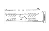
図6及び図7は、本発明の第2の実施形態に係わる半導体記憶装置を示す回路構成図であり、特に強誘電体メモリのブロック構成を示している。
【0117】
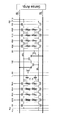
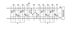
図6が図1と異なる点は、ブロックユニットの直列セル数を8個に増やしたことにある。これにより、プレート選択信号,ブロック書き込み選択信号,増幅トランジスタ等の1セル当りのオーバヘッドを半減できる。また、今まで述べたように、強誘電体キャパシタ面積によって、最適な負荷容量CLを図4及び図5の例のように変えることができる。これにより、サブビット線に読み出される信号量を常にどの世代でも確保でき、これを増幅トランジスタでビット線を駆動すれば正常動作が可能となる。それ以外の効果は、図1と同様である。
【0118】
図7が図1と異なる点は、ブロックユニットの直列セル数を16個に増やしたことにある。これにより、上に説明したように、1セル当りのオーバヘッドを半減でき、最適な負荷容量CLを変えることができる。このように、ブロックユニットの直列セル数は自由に変えることができる。図では示さないが、直列セル数=32,64,128,256等も可能である。それ以外の効果は、図1と同様である。
【0119】
(第3の実施形態)
図8は、本発明の第3の実施形態に係わる半導体記憶装置を示す回路構成図であり、特に強誘電体メモリのメモリマット(セルアレイ)全体の構成を示している。
【0120】
本実施形態では、図1に示したセルブロックを2次元配置して、ロウデコーダとセンスアンプ(SA0〜SAn-1 )を接続した例を示す。ロウデコーダの替わりに階層ワード線方式を適用して、サブロウデコーダにしても良い。図8のプレート線PLB,/PLBに示すように、左右のセルブロックでプレート線を共有することにより、アレイサイズを小さくできる上、プレート駆動回路面積を小さくできる。逆に言えば、駆動能力を上げることができる。センスアンプ回路に従来FRAMと同様なフリップフロップ型センスアンプ回路が適用できる。但し、図2、図3の動作の例の場合は、ビット線のプリチャージは (1/2VBLH),VBLHH になるように設計する。それ以外の効果は、図1と同様である。
【0121】
(第4の実施形態)
図9(a)(b)は、本発明の第4の実施形態に係わる半導体記憶装置を示す回路構成図であり、特にセンスアンプ構成とセルアレイのブロック構成を示している。この図の例においては、図1に示したような複数の自己増幅機能を持つセルブロック(GainCellBlock0〜n-1 )ビット線/BL,BLに接続して、ビット線対を構成して、ここでは省略しているが、これをワード線方向に複数配置してアレイを構成する。各ビット線対は、φt0をゲート入力とするアレイ−センスアンプ分離トランジスタを介してセンスアンプ回路に接続している。
【0122】
(b)の例では、センスアンプ回路の右側にもセルアレイが配置されており、同様に、φt1をゲート入力とするアレイ−センスアンプ分離トランジスタを介してセンスアンプ回路に接続している点が(a)と異なる。(b)の回路は、左右のセルアレイでセンスアンプ回路を共有している。(a)は共有しない例であり、φt0をゲート入力とするアレイ−センスアンプ分離トランジスタが無くても良い。(a)(b)の例では、ダミーセルはセンスアンプ内に配置され、(b)の例ではダミーセルも左右のセルアレイで共有できることを意味する。
【0123】
(a)(b)センスアンプ回路は、図2の動作を実現できる。/EQL信号はビット線対をイコライズすると同時に、VBL(=(1/2)VBLH)にプリチャージする。SEN,/SEPはnMOS,PMOSトランジスタからなるフリップフロップアンプを動作させる。CSLはカラム選択信号であり、センスアンプで増幅した信号線(/BLSA,BLSA)のデータをデータ線/DQ,DQに伝送する、或いは/DQ,DQからデータを書き込むためにある。なおVBLの電位を VBLH に設定すれは、図3の動作が実現できる。
【0124】
図10は、図9の実施形態の具体的な動作例を示す信号波形図である。これは、図1のセルブロックで図9のアレイ構成での動作例を示し、図2の動作例に図9の信号線の動作を加えたものを示している。
【0125】
図2の動作に加え、プレート/PLA,PLA選択前に、/EQLを下げ、ビット線/BL,BLのイコライズを解除すると同時に、選択しないセンスアンプの右のセルアレイとセンスアンプを切り離すため、φt1をLowにする。センスアンプ活性化は、サブビット線/SBLの信号により、増幅トランジスタに電流が流れ、ビット線対/BL,BLに電位差が十分発生した後、SENをHigh、/SEPをLowにすることにより、フリップフロップ型センスアンプが動作する。ブロック書き込み選択信号BS0をOFFした後、SENをLow、/SEPをHighにしてセンス動作は修了する。その後、/EQLをHigh、φt1をHighにして、スタンドバイ状態になる。
【0126】
(第5の実施形態)
図11は、本発明の第5の実施形態に係わる半導体記憶装置を示す回路構成図であり、特にセンスアンプ構成とセルアレイのブロック構成を示している。
【0127】
本実施形態は基本的には図9の例と同じであるが、図9と異なる点は、ダミーセルがセルアレイ側にあることである。これは、セルアレイのセルと同様なプロセス,構造のダミーセルを構成するのに適している。
【0128】
(第6の実施形態)
図12(a)〜(c)は、本発明の第12の実施形態に係わる半導体記憶装置を示す回路構成図であり、特にダミーセル構成を示している。この実施形態は、図1の実施形態及びそれ以後の実施形態に適用できる構成である。
【0129】
本実施形態のダミーセルは、図9に示すセンスアンプのビット線/BLSA,BLSAに接続している。図11のセルアレイ内部でも良い。図12(a)のダミーセルは、単純にキャパシタを用いて、カップリングによりリファレンスビット線の電位を発生する。
【0130】
図13は、図12(a)のダミーセルの動作例を示す信号波形図である。これは、図1の回路例でしかも、図2の動作例の場合を示す。BLSA側にセルデータが読み出され、BLSAが“1”データの時、VBLHから下がり (1/2)VBLH−2Vsになる。“0”データの時、(1/2)VBLHの状態のまま2つの状態の中間値に、リファレンスビット線/BLSAがなるように、即ち (1/2)VBLH−Vsになるように、VDWL0の電位を下げ、ダミーキャパシタのカップリングにより/BLSAの電位を下げる。センスアンプでビット線対を増幅した後は、VWDL0を上げ元に戻して良い。
【0131】
図12(b)は、図12(a)と同様にキャパシタカップリング方式のダミーセルである。ダミーキャパシタと、両端をショートしリセットするトランジスタQ10と信号RSTと、ダミーキャパシタをビット線と接続するトランジスタQ11,Q12とダミーワード線VDWL0,VDWL1から構成している。MOSゲートキャパシタでダミーキャパシタ形成した場合に面積が大きくなる問題に対して、ダミーキャパタをビット線対で共有し面積を削減している。
【0132】
図14は、図12(b)のダミーセルの動作例を示す信号波形図である。ダミーセルデータを読み出す前に、RSTをLowにして、ダミーキャパシタのショートを解除してから、VDWL0をHighにすると、VDPL電位が (1/2)VBLHより低い場合、キャパシタのカップリング分だけ/BLSA電位が下がり、リファレンス電位となり得る。その他、応用例として図14でDPLをクロッキングしても良い。
【0133】
図12(c)は、図12(b)と同様にキャパシタカップリング方式のダミーセルである。異なる点は、2種類のダミーキャパシタCD0とCVD1がある点である。
【0134】
図15は、図12(c)のダミーセルの動作例を示す信号波形図である。図4で示したように、選択したワード線の位置により負荷容量CL(=CSBL)が異なり、サブビット線の電位が異なり、結果として、ビット線BLの下がる程度が異なる問題をこれは解決できる。即ち、CD0とCD1の容量を変え、選択したワード線の位置により図15のようにRST0を下げるか、RST1を下げるか変えることにより、CLが変わる問題を量子的ではあるが解決できる。さらにCDiの数を増やせば、細かく制御可能である。図13(a)〜(c)の例は常誘電体キャパシタを用いていたが、強誘電体キャパシタでも構成可能である。
【0135】
(第7の実施形態)
図16(a)〜(c)は、本発明の第7の実施形態に係わる半導体記憶装置を示す回路構成図であり、特にダミーセル構成を示している。この実施形態は、図1の実施形態及び、以後の実施形態に適用できるダミーセル構成を示し、定電流型ダミーセルを示している。
【0136】
図16(a)は、2個のトランジスタでダミーセルを構成している。図17は、図16(a)のダミーセルの動作例を示す信号波形図である。図1のトランジスタQ5がONし、”1”データがBLSAに読み出され、BLSA電位が下がる場合のトランジスタQ5に流れる電流をIとした場合、VDWL0がHighになり、トランジスタQ13がONし/BLSAからVDSEに流れる電流を (1/2)Iに設定すれば、リファレンスが生成できる。
【0137】
図12のダミーセルは、時間と共にセルデータが読み出されるビット線BLSAの電位が下がるのに対して、リファレンス電位は固定のため、一定時間後センスする必要があった。しかし、図16の場合は、常にリファレンス電位は“1”と“0”データの中間値に設定できるメリットがある。 (1/2)Iの設定は、VDSEの電位、VDWL0のHighの電位及び、トランジスタQ13のサイズで調整できる。
【0138】
図16(b)は、図16(a)に比べ精度調整が可能な例を示す。図18は、図16(b)のダミーセルの動作例を示す信号波形図である。トランジスタQ14よりトランジスタQ15の駆動能力を大きく設定して、 (1/2)I電流が、トランジスタQ14で制限されるようにし、トランジスタQ14の電流もVDC,VDSE電位で決まるようにしておき、VDWL0をHighにして、 (1/2)Iが流れるようにする。VDC,VDSE電位をアレイ外部からヒューズ等で微調整できるようにすれば、精度が上がる。
【0139】
図16(c)は、図16(b)の定電流方式のダミーセルを複数個用意した場合を示す。図19は、図16(c)のダミーセルの動作例を示す信号波形図である。図12(c)と同様にどちらか一方を選択して、選択したワード線の位置により読み出し信号が異なる問題を回避している。どちらか一方ばかりでなく両方を選択するようにすれば、より細分化できる。
【0140】
(第8の実施形態)
図20は、本発明の第8の実施形態に係わる半導体記憶装置を示す回路構成図であり、特にダミーセル構成を示している。この実施形態は、図1の実施形態及び、以後の実施形態に適用できるダミーセル構成である。この例は、ダミーキャパシタとして、セルアレイと同じ強誘電体キャパシタを用いた例であり、図4で示した選択したワード線の位置により、図1の負荷容量CLが異なりサブビット線SBLの電位が異なる問題を解決できる。
【0141】
図20において、左上下のブロックユニットは、図1と同じ構成で、ダミーワード線に接続され、左端はダミープレートDPL,DPLに直接接続されている。右上下のブロックユニットは選択せずVPPに接続されて、リセットトランジスタQ16,Q17を介して固定電位Vss’に接続されている。ブロック書き込み選択信号及びこのトランジスタは無く、増幅トランジスタのみ存在する構成である。
【0142】
図21は、図20のダミーセルの動作例を示す信号波形図である。DRST0を下げ、選択ワード線に対応する位置のダミーワード線を下げ、ダミーサブビット線/DSBL,DSBLをフローティングにする。その後、DPLを上げると、“0”データがDSBLに読み出され、増幅トランジスタQ18がONし、 (1/2)Iの電流が流れ、リファレンスビット線/BLの電位が下がりリファレンス電位が発生するしくみである。その後、DPLがHighのまま、DRSTを上げると、選択したダミーセルの強誘電体キャパシタにDPL−Vss’の電位が書き込まれ“0”データがもとに戻される。その後、DPLを下げ、DWL0を上げてスタンドバイ時の状態に戻る。
【0143】
この場合、ダミーセルの“0”データ読み出しによるDSBLの電位と、図1の“0”データ読み出しのSBLの電位は、選択したワード線の位置に拘わらず同じになる。このとき、図20の増幅トランジスタQ18のW/L比を図1のトランジスタQ5のW/Lに比べて大きく設定しておけば、リファレンス電位が容易に発生できる。
【0144】
またその他の方式として、Vss’の電位をVssより高めに設定すると、図22の動作点設計指針の点線の負荷直線に示すように、トランジスタQ18とトランジスタQ5が同じサイズのままでも、常にダミーセルの動作点は、通常セルの動作点より右側になる。この“0”データ書き込みダミーセル方式は、ダミー強誘電体キャパシタの分極反転を伴うことが無いため、通常セルより選択回数が多くても、疲労による劣化の問題を回避できる。
【0145】
またその他の応用例として、Vss’=Vssのままで、トランジスタQ18とトランジスタQ5のサイズを同じままでも、右上下のブロックユニットの負荷容量小さくすれば、“0”データの動作点は、通常セルよりダミーセルが右側になる。例えば、右上下のブロックユニットの直列数を半減する等の方法が良い。
【0146】
その他の方式として、ダミーセルとして“1”データを常に読み出す方式も可能である。例えば、DPLを下げた後、Vss’を上げ下げすることにより“1”データがダミーの強誘電体キャパシタに書き込まれる。読み出しは、右のDSBL側の負荷容量を通常セルより大きくすれば、リファレンスとなりうる。又は、同じ構成で、Vss’のHigh電位を通常セルより下げたり、トランジスタQ19のサイズをトランジスタQ5のサイズより小さくすれば容易にリファレンスが発生できる。また、右の上下の2個ブロックユニットを合体して負荷容量を増大することもできる。
【0147】
(第9の実施形態)
図23は、本発明の第9の実施形態に係わる半導体記憶装置を示す回路構成図であり、特に強誘電体メモリのセルブロック,セルアレイ,センスアンプ構成を示している。この図は、図1の構成よりもより概念的な構成を示している。
【0148】
セルトランジスタと強誘電体キャパシタを並列接続して1個のセルを構成し、これを直列接続してブロックユニットを構成している。ブロックユニットの一端はPL駆動回路に接続され、他端は増幅回路及び書き込み回路を介してビット線/BL,BLに接続され、ビット線には複数のセルブロックが接続され、ビット線の端はセンスアンプ回路に接続されている。
【0149】
この実施形態では、選択したワード線を下げ、PL駆動回路でブロックユニットに電圧を印加して、サブビット線/SBL或いはSBLにセル電荷を読み出し、これを増幅回路で増幅して、ビット線/BL或いはBLに信号を伝えセンスアンプで増幅して、これを書き込み回路でサブビット線/SBL或いはSBLに書き戻し、セルに書き戻す方式である。これによる効果は、図1と同様である。1トランジスタ+1キャパシタ構成でなく、上下のブロックユニットの両方からセルデータを読み出す、2トランジスタ+2キャパシタ構成も可能である。この場合はダミーセルは不要である。
【0150】
(第10の実施形態)
図24は、本発明の第10の実施形態に係わる半導体記憶装置を説明するためのもので、特に複数の強誘電体メモリアレイと複数のセンスアンプ配置例を示している。この例は、図1の実施形態はもとより他の実施形態にも適用できるものである。前記した図1の効果のまとめ5)で示したように、本発明を適用することにより、セルブロック内のサブビット線の負荷容量によりサブビット線の読み出し電位が決まり、これを増幅トランジスタを用いてビット線を駆動するため、読み出し時間さえあれば、ビット線の寄生容量はいくら大きくても読み出せる。
【0151】
図24(a)は従来セルアレイとセンスアンプ配置を示し、(b)は本実施形態の構成例を示す、ビット線につながるセル数を多くできることにより、結果としてセンスアンプ数を激減でき、チップサイズの低減、即ちチップ内のセル占有率を上げることができる。なお、時間をかければと述べたが、本発明においては、セルブロック毎に2個のトランジスタのみビット線につながるため、従来の1トランジスタ+1キャパシタのセルに比べてビット線容量/cellが1/2〜1/4程度と小さいので、センスアンプ数は元々、同じパワー、ほぼ同じ充電放電時間でも同じ時間で動作が可能である。さらに、自己ブロック増幅効果によりセンスアンプ数を低減できるわけである。
【0152】
(第11の実施形態)
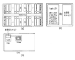
図25は、本発明の第11の実施形態に係わる半導体記憶装置を説明するためのもので、メモリチップ構成例、ロジック混載構成例、RF−IDカード構成例を示している。この例は、図1の実施形態はもとより他の実施形態にも適用できるものである。
【0153】
図25(a)はメモリチップ構成例であり、チップにはセルアレイ,センスアンプばかりでなく、少なくともロウデコーダ(R/D),カラムデコーダ(C/D),周辺回路等が設けられている。図25(b)はロジック混載構成の場合であり、本発明のメモリと各種ロジックLSIの混載で構成される。ロジックLSIが限界で無く、従来メモリに限界(読み出し安定動作限界或いはコスト限界)が来た場合でも、本発明には限界が来ない場合、この構成が有効である。図25(c)はRFーIDカード構成の場合であり、本発明のメモリとロジックLSI及びアンテナで構成される。
【0154】
(第12の実施形態)
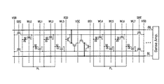
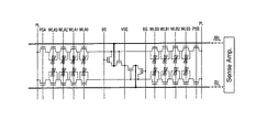
図26は、本発明の第12の実施形態に係わる半導体記憶装置を示す回路構成図であり、特に強誘電体メモリのブロック構成を示している。図1とほぼ同一の構成であり、殆どの効果が図1と同じである。異なる点は、上の左右のブロックユニットに接続されるサブビット線/SBLをゲート入力とする増幅トランジスタQ20のソースがビット線/BL側に接続され、ドレインがVSE電位に接続される。さらに、下の左右のブロックユニットに接続されるサブビット線SBLをゲート入力とする増幅トランジスタQ21のソースがビット線BL側に接続され、ドレインがVSE電位に接続される点である。即ち、読み出すビット線と書き込みを行うビット線が同じビット線/BL或いはBLである点である。
【0155】
図27は、図26の具体的な動作例を示す信号波形図である。まず、スタンドバイ時は、全てのワード線WLA0〜3、WLB0〜3は昇圧電位Vpp、全てのプレート/PLA,PLA,/PLB,PLBは0V、プレート選択信号PSA,PLBをVppにしておくことにより、セルトランジスタは全てONしており、全てのセルの強誘電体キャパシタの両端は電気的にショートされて、さらにこの両端の電位及びサブビット線/SBL,SBLの電位は、プレート選択信号がHighのため、プレートに接続され0Vになっている。
【0156】
また、ブロック書き込み選択信号BS0,BS1は0Vにしておくことにより、トランジスタQ22,Q23はOFFしており、/SBL,SBLが0Vのため、VSEが VBLH と高い電位であっても、増幅トランジスタQ20,Q21もOFFしている。よって、ビット線/BL,BLとサブビット線/SBL,SBLは完全に分離されている。
【0157】
この動作例の場合、ビット線/BL,BLのプリチャージ電位は0Vである。動作時は、選択したセルブロックの、例えば左上のブロックユニットのメモリセル(Q24,CF2)選択時の動作を説明する。まず、選択メモリセルにつながるワード線WLA0を0Vに下げセルトランジスタQ24をOFFする。同時に或いは前後して、右上,右下のブロックユニットとプレート/PLB,PLBを切り離すため、プレート選択信号PSBを0Vに下げトランジスタQ25,Q26をOFFする。さらに、ビット線/BL,BLを0Vのままフローティングにする。ここで、Q27,Q28はONのままである。
【0158】
これにより、セルトランジスタQ24はOFF、トランジスタQ25はOFFしているため、選択したセルの強誘電体キャパシタCF2の右側の端子から/SBL、さらに右上のブロックユニットのセル内部ノードは全てつながり、かつ0Vでフローティングになる。
【0159】
次に、選択した左上のブロックユニットに接続されるプレート/PLAのみを0Vから VBLH に上げる。PLAから選択した強誘電体キャパシタの左側端子まで VBLH 電位が印加される。このとき、CF2の右側の端子から/SBL、さらに右上のブロックユニットのセル内部ノードの容量が負荷容量CLとなり、強誘電体キャパシタに“1”データが書き込んであれば、分極反転して、セルデータがサブビット線/SBL(正確には、CF2の右側の端子から/SBL、さらに、右上のブロックユニットのセル内部ノード)に読み出され/SBLの電位が0Vから2Vs+Voに上がる。
【0160】
強誘電体キャパシタに“0”データが書き込んであれば、分極反転せず、CF2の常誘電体成分容量とCLの容量比分だけ、サブビット線/SBLの電位上がり、/SBLの電位はVoとなる。このとき、対をなすサブビット線SBLの電位はPLAが0Vのままなので、0Vのままである。ここで、VSE電位を VBLH に設定しておくと、増幅トランジスタQ20のゲート電位は“1”データ時は2Vs+Vo、“0”データ時はVo、ドレイン電位(=VSE)は VBLH 、ドレイン電位(=/BL)は0Vとなる。
【0161】
トランジスタQ20のしきい値電圧VtをVo<Vt<2Vs+Voに設計しておくと、図27に示すように、“1”データ時、トランジスタQ20はONしているため、0Vにプリチャージされている/BLは増幅トランジスタQ20を介して、VSEに電流が流込むことにより、0Vから電位が上がり始める。ここで、センスアンプ動作前の上がった電位を0V+2Vst定義する。逆に、“0”データ時、トランジスタQ20はOFFしているため、0Vにプリチャージされている/BLは増幅トランジスタQ20を介して、VSEから電流が流れず、0Vのままである。
【0162】
このとき、定電流駆動トランジスタを用いたダミーセル等を用いて、BL電位を“1”データ時BL側が上がる電位の半分の電位上げるように設定すると(即ちセンス動作前、0V+Vst)、センスアンプ動作前、“1”データ時、/BLは0V+2Vst、BLは0V+VstとなりVstの電位差が図26の右のセンスアンプに入力され、フリップフロップ型のセンスアンプで増幅され、BLは0V、/BLは VBLH となる。また、“0”データ時、/B2kは0V、BLは0V+VstとなりVstの電位差が図26の右のセンスアンプに入力され、フリップフロップ型のセンスアンプで増幅され、BLは VBLH 、/BLは0Vとなる。
【0163】
なお、図27の例ではビット線対は0Vにプリチャージにしてあったが、ある一定の電位VBLでも良いし、 (1/2)VBLHにしてもよい。この場合、増幅トランジスタQ20,Q21が“1”データ時ONし、“0”データ時OFFするように、増幅トランジスタのしきい値電圧VtをVo−VBL<Vt<Vo+2Vs−VBLになるように設計する必要がある。
【0164】
或いは、ONするが電流の違いをセンスアンプで検知する場合は、Vt<Vo−VBLに設計する必要がある。但し、本実施形態は図1と異なり、増幅トランジスタのソース側がビット線となるため、ソース電位が変わる問題を持つ。例えば“1”データ時/BLが上がり始めるとソース電位が上がり増幅トランジスタは途中でOFFする。また、“0”データ時、/BLを0Vプリチャージ以外にしておくと、センスアンプでの増幅で、/BLが下がると、増幅トランジスタがONしてしまう問題がある。
【0165】
後半の問題は図27の0Vビット線プリチャージ方式で回避できるし、前半の問題は、確かに図1に比べて読み出し信号量は減るが、サブビット線に読み出される信号量は大きく、この分だけ、ビット線対の電位差が開いてから増幅トランジスタがOFFするため問題ない。しかも、一定の所でビット線対の電位差が止るため、図12に示したキャパシタカップリング型のダミーセルに適している。逆に言うと、図1の方式は、図16、図20等の定電流型ダミーセルが適していることを示している。なお、VSEの電位は VBLH でも良いし、ビット線のプリチャージ電位より高ければ何でも良い。
【0166】
データの再書き込み時、サブビット線/SBLに接続されるブロック書き込み制御信号BS0のみVppに上げる。すると、0V或いは VBLH に増幅されたビット線/BLの電位が/SBLに書き込まれ、“1”データ時、/SBLは VBLH となり、“0”データ時/SBLは0Vになる。このとき、プレート電位(=選択強誘電体キャパシタの左側の端子)は VBLH のため、“0”データ時、強誘電体キャパシタには−VBLHの電圧(強誘電体キャパシタの右側の端子を正と定義)が印加され、“0”データが再書き込みされる。“1”データ時は、その後、プレート/PLAが0Vに下げられ、選択強誘電体キャパシタの左側の端子も0Vになった時、強誘電体キャパシタには VBLH の電圧(強誘電体キャパシタの右側の端子を正と定義)が印加され、“1”データが再書き込みされる。
【0167】
これら一連の動作において、SBL電位はずっと0Vのままなので、下のブロックユニットのデータは保持されたまま、安定である。例えば、外部から異なるデータを書き込む場合(ライト・モード)や、データの読み出し後外部データを書き込む場合(リード・モディファイ・モード)、BS0がHighになったあと書き込めば良い。
【0168】
再書き込み終了後は、まずブロック書き込み選択信号BS0をHighから0Vに下げる。これにより、/BL側から/SBLへの干渉は無くなる。その後、WLA0を上げ、同時に或いは前後して、プレート制御信号PSAを上げると、選択されていたセルの強誘電体キャパシタは電気的にショートされ、右上,左上のブロックユニットの内部ノードと/SBLノードは0Vになる。これら動作と同時に或いは前後して、ビット線対/BL,BLを0Vに下げると、スタンドバイ状態に戻る。
【0169】
以上述べたように図26の構成は図1とほぼ同じで、その効果をまとめると、
1)先願と同様に、4F2 サイズの高密度のセルを実現しつつ、平面トランジスタで製造の容易化を実現し、さらに高速なランダムアクセス機能を有することが可能。
【0170】
2)設計ルールが縮小して、強誘電体キャパシタ面積が縮小しても、それに合わせて分極反転時の負荷容量であるサブビット線容量が低減でき、十分な読み出し信号電圧が得られ、増幅トランジスタを用いてビット線を増幅するため、安定動作が可能。
【0171】
3)従来FRAMと同様動作原理が単純で、しかも高速プレート動作により、高速動作が可能。
【0172】
4)ビット線容量が大きくても読み出し可能であるため、ビット線に接続できるセルブロック数を多くでき、結果としてセンスアンプ面積を低減できる。
【0173】
5)ルール縮小により、強誘電体キャパシタの分極量の減少に合わせて、ブロックユニット内の直列セル数を減らせば、最適化が可能。
【0174】
6)設計ルールが緩く、ソフトエラーが厳しい状況では、ブロックユニットの直列セル数を増加させ、負荷容量を追加して読み出し電荷を増やせば、ソフトエラーを抑えられ、設計ルールが小さくなるに従って、ソフトエラーレートが下がるに従って、ソフトエラーが問題無い程度に、強誘電体キャパシタサイズと、直列セル数を徐々に減らして、サブビット線に読み出される信号量を確保すれば、良い。
【0175】
7)ブロックユニット内の複数のセルで、増幅トランジスタと、書き込みトランジスタを共用することにより、セルサイズのオーバヘッドを極めて小さなものにできる。
【0176】
8)左右のブロックユニットで増幅トランジスタや、ブロック書き込み選択トランジスタを共有すれば、さらにこれらのオーバヘッドは小さい。
【0177】
9)分極反転のための負荷容量として、選択したブロックユニットの反対側のブロックユニットの内部容量を用いることにより、ほぼ安定に動作が可能。
【0178】
10)ブロックユニットのセル数を変えることにより、自由に負荷容量の調整が可能。
【0179】
11)サブビット線の信号でビット線対の同じ側のビット線を増幅トランジスタで駆動することによりビット線に一定量の電位差が発生し、簡単なキャパシタカップリング型のダミーセルが利用し易い。
【0180】
(第13の実施形態)
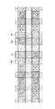
図28は、本発明の第13の実施形態に係わる半導体記憶装置を示す平面図であり、特に強誘電体メモリのブロック構成のレイアウトを示している。図28(a)は図1の回路図に対応して、トランジスタの位置も図1と同じ配置である。図28(b)は図26の回路図に対応して、トランジスタの位置も図26と同じ配置である。このように、図1、図26は等価回路自身でも本発明の効果があるばかりでなく、トポロジ的にも細密配置の効果がある。
【0181】
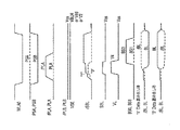
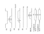
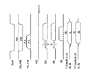
図29は、図28(a)の増幅トランジスタとブロック書き込み選択トランジスタ部分の拡大レイアウト図である。複数層重ねると判りにくいため、同じレイアウトの各層を図30から図32に分けて表示してある。各レイヤ表示として、拡散層をAA、ゲート層をGC、上部電極層をTE、下部電極層をBE、強誘電体層をFE、ビット線層をBL、拡散層−下部電極層間コンタクトをAA−BE−C、拡散層−上部電極層間コンタクトをAA−TE−C、ゲート層−下部電極層間コンタクトをGC−BE−C、上部電極層−ビット線層間コンタクトをTE−BE−Cと定義している。上部電極層,下部電極層は強誘電体キャパシタの上下電極層を意味する。
【0182】
図30において、Q6,Q5が増幅トランジスタのチャネル部を示し、Q7,Q8がブロック書き込み選択トランジスタのチャネル部を示す。サブビット線/SBL,SBLは図31に示すように、下部電極層(BE)を引き回すことにより、容易にビット線となるビット線層(BL)の下に形成できる。図29から図32で判るように、増幅トランジスタとブロック書き込み選択トランジスタを左右のブロックユニットにより素子数を減らし、さらにVSE端子部は増幅トランジスタQ6,Q5のソースを共有し、また増幅トランジスタのドレインとブロック書き込み選択トランジスタのドレインで拡散層を共有し、さらにセルトランジスタのドレインとブロック書き込み選択トランジスタのソースで拡散層を共有するため、非常にコンパクトなレイアウトになっている。
【0183】
図28において、セルサイズを4F2 とすると、プレート駆動部,増幅トランジスタ部,ブロック書き込み選択トランジスタ部を含む、ブロック平均のセルサイズは、ブロックユニットのセル直列接続数が16直列で、5F2 サイズ、32直列で4.5F2 サイズ、64直列で4.25F2 サイズと、自己増幅機能があるにも係らず極めて小さなセルとなる。また、セルアレイ内でピッチが厳しいにも拘わらず、無理なく自己増幅機能を実現するトランジスタが配置できている。
【0184】
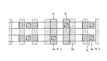
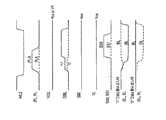
図33は、図28(b)の増幅トランジスタとブロック書き込み選択トランジスタ部分の拡大レイアウト図である。複数層重ねると判りにくいため、同じレイアウトの各層を図34から図36に分けて表示してある。レイヤ構成及びレイヤの別けかたは、図30から図33と同じである。図26の回路構成を実現するには、図30におけるトランジスタQ5、Q6のトランジスタのGC、GC−BE−Cをチャネルを中心に上下の折り返すだけで実現できている。
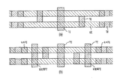
【0185】
図37は、図28(a)(b)に共通のプレート選択トランジスタとプレート線の部分の拡大レイアウト図である。図38及び図39は、図37のレイアウトの一部の層のレイアウトを示す。プレート線も隣接のセルブロックで共有することにより、この部分の面積を半減できている。図37で/PLB’側が隣接する他のセルブロック部である。プレート線にはTEを用いて、2ビット線毎に、拡散層AAとコンタクトを取ることにより、フォールデッドBL方式を実現している。
【0186】
(第14の実施形態)
図40〜図43は、本発明の第14の実施形態に係わる半導体記憶装置を示す素子構造断面図であり、特に強誘電体メモリのブロック構成例を示している。
【0187】
図40は28(a)のレイアウト構成の左側の断面図に対応し、図41は28(a)のレイアウト構成の右側の断面図に対応している。図40及び図41の各図(a),(b),(c)は、ビット線方向で、/BL中央,/BLとBLの中間,BL中央で割った時の断面図に対応する。BEを巧みに用いることによりコンパクトで、設計余裕がありつつ自己増幅機能を実現していることが判る。
【0188】
図42及び図43は、構成が図40及び図41と類似しているがこれらと大きく異なる点は、強誘電体キャパシタが下部電極間に形成されている点である。これにより、メモリセル部の強誘電体キャパシタがセルフアラインで形成されるメリットがある。サブビット線の配線はBEで配設できていることが判る。
【0189】
(第15の実施形態)
図44は、本発明の第15の実施形態に係わる半導体記憶装置を示す回路構成図であり、特に強誘電体メモリのブロック構成を示している。本実施形態の回路構成及び効果は、図1とほぼ同じである。図1と異なる点は、サブビット線/SBL,SBLに負荷容量安定用キャパシタC10を接続して、他端を固定電位VLに接続した点である。
【0190】
固定の安定負荷容量を追加することにより、図4で示した、選択したワード線の位置により負荷容量が変化して、動作点がずれる問題を克服できる。さらに、デバイスの縮小がそれ程進んでいなく、反対側のブロックユニットだけでは、負荷容量が不足する場合にも適用できる。また、デバイスの縮小がそれ程進んでいなく、負荷容量を稼ぐために、ブロックユニットのセル数を多くして、読み出し遅延が増大するのも防げる。
【0191】
図45は、図44の具体的な動作例を示す信号波形図である。これは、(1/2)VBLHプリチャージ方式の場合で、図2と動作は同じである。図46は、図44の具体的な別の動作例を示す信号波形図である。これは、 VBLHプリチャージ方式の場合で、図3と動作は同じである。但し、サブビット線の読み出し電位は負荷容量変化により異なる。
【0192】
(第16の実施形態)
図47は、本発明の第16の実施形態に係わる半導体記憶装置を示す回路構成図であり、特に強誘電体メモリのブロック構成を示している。これは、図26の構成に負荷容量C10を追加した場合を示している。効果は、図44と同じである。図48は、図47の具体的な動作例を示す信号波形図である。Vssビット線プリチャージ方式を示し、図27と動作は同じである。
【0193】
図49は、図47の具体的な別の動作例を示す信号波形図である。これは、ビット線 (1/2)VBLHプリチャージ方式を示す。図27の説明で示した増幅トランジスタのしきい値を変えて、ビット線 (1/2)VBLHプリチャージ方式を実現しても良いし、図49に示すように、増幅トランジスタ動作時にVL線を持ち上げて、サブビット線電位を上げ、増幅トランジスタをONさせても良い。
【0194】
(第17の実施形態)
図50及び図51は、本発明の第17の実施形態に係わる半導体記憶装置を示す回路構成図であり、特に強誘電体メモリのブロック構成を示している。図50の構成は、図44の負荷容量を強誘電体キャパシタで実現した場合である。図51の構成は、図47の負荷容量を強誘電体キャパシタで実現した場合である。
【0195】
強誘電体キャパシタには常に正或いは負のバイアスしかかからないように設計すれば、分極反転することなく、負荷容量として利用できる。例えば、VLをVssに設定して、メモリ出荷前に一度動作させ、サブビット線を VBLH にしておけば、その後Zこの強誘電体キャパシタが分極反転することは無くなる。
【0196】
(第18の実施形態)
図52は、本発明の第18の実施形態に係わる半導体記憶装置を示す平面図であり、特に強誘電体メモリのブロック構成のレイアウトを示している。これは、ブロック書き込み選択トランジスタ及び増幅トランジスタ部分のレイアウトを示している。
【0197】
図53は図52のレイアウト図の一部レイヤ層を表示したものであり、図54は図52のレイアウト図の一部レイヤ層を表示したものである。図52〜図54において、(a)は、図29と対比して、増幅トランジスタのサイズのチャネル長L側を大きくした場合を示す、これにより、サブビット線の負荷容量の一定成分が増加できる。(b)は、図44に対応して、強誘電体の安定用キャパシタを追加した場合を示している。この例では、1セルブロックに4個の安定用FEを追加している。
【0198】
(第19の実施形態)
図55は、本発明の第19の実施形態に係わる半導体記憶装置を示す回路構成図であり、特に強誘電体メモリのブロック構成を示している。これは、図1のセルブロックから右上下のブロックユニットを取り除いた構成のものであり、殆どの効果は図1と同じである。左右のブロックユニットの選択が無い分、プレート選択信号及びプレート選択トランジスタが不要になり、プレートはブロックユニットに直に接続される。図4で示した選択するワード線の位置による負荷容量の変化が激しいが、これはダミーセルで対応できるし、図52(a)のようなトランジスタサイズを大きくして対応できる。
【0199】
図56は、図55の具体的な動作例を示す信号波形図である。WL0を下げ、/PLを上げるだけで、サブビット線/SBLにデータが読み出され、増幅トランジスタを介してこのデータはビット線対の反対のビット線BLに読み出され、センスアンプで増幅される。増幅後のデータは、ブロック書き込み選択信号BS0をHighにすることでサブビット線に戻され、/PLをHighからLowに駆動することにより、“1”,“0”データがセルに書き戻される。その後、BS0を下げ、WL0を上げると、自動的にサブビット線の全てのノードはVssになる。ビット線もイコライズすることにより、図1と同様 (1/2)VBLHに戻され、スタンドバイ状態になる。
【0200】
図57は、図55の具体的な別の動作例を示す信号波形図である。図56と異なる点は、ビット線が VBLH 電位プリチャージである点のみである。このように、図1とほぼ同様な効果、ほぼ同様な動作が可能となる。
【0201】
(第20の実施形態)
図58は、本発明の第20の実施形態に係わる半導体記憶装置を示す回路構成図であり、特に強誘電体メモリのブロック構成を示している。図55と異なる点は、図1と図26の違いと同様、増幅トランジスタがつながるビット線が、書き込み用ビット線と同じである点である。
【0202】
図59は、図58の具体的な動作例を示す信号波形図である。Vssビット線プリチャージにより、図27と図56を足し合せた動作が可能である。
【0203】
(第21の実施形態)
図60は、本発明の第21の実施形態に係わる半導体記憶装置を示す回路構成図であり、特に強誘電体メモリのブロック構成を示している。図55の構成とことなる点は、負荷容量安定用常誘電体キャパシタが追加された点である。
【0204】
図61は図60の具体的な動作例を示す信号波形図であり、図62は図60の具体的な動作例を示す信号波形図である。それぞれ図56、図57と同じ動作が可能で、サブビット線の読み出し電位のみ異なる。
【0205】
(第22の実施形態)
図63は、本発明の第22の実施形態に係わる半導体記憶装置を示す回路構成図であり、特に強誘電体メモリのブロック構成を示している。これは、図58と同様の構成で、図58の構成と異なる点は、負荷容量安定用常誘電体キャパシタが追加された点である。
【0206】
図64は、図63の具体的な動作例を示す信号波形図である。これは、図59と同じ動作が可能で、サブビット線の読み出し電位のみ異なる。
【0207】
(第23の実施形態)
図65〜図78は、本発明の第23の実施形態に係わる半導体記憶装置を示す回路構成図であり、特に強誘電体メモリのブロック構成を示している。図65の構成は、図60の常誘電体キャパシタの負荷容量の替わりに強誘電体キャパシタを用いた点のみ異なる。図66の構成は、図63の常誘電体キャパシタの負荷容量の替わりに強誘電体キャパシタを用いた点のみ異なる。
【0208】
図67の構成は、これは図55と等価回路は同じ、効果も同じであるが、トランジスタ配置位置のトポロジが異なる。ブロック書き込み選択トランジスタと増幅トランジスタを分けて配置している。図68の構成は、図60と等価回路は同じ、効果も同じであるが、トランジスタ配置位置のトポロジが異なる。
【0209】
図69の構成は、図65と等価回路は同じ、効果も同じであるが、トランジスタ配置位置のトポロジが異なる。図70の構成は、図58と等価回路は同じ、効果も同じであるが、トランジスタ配置位置のトポロジが異なる。ブロック書き込み選択トランジスタと増幅トランジスタを分けて配置している。
【0210】
図71の構成は、図63と等価回路は同じ、効果も同じであるが、トランジスタ配置位置のトポロジが異なる。図72の構成は、図66と等価回路は同じ、効果も同じであるが、トランジスタ配置位置のトポロジが異なる。
【0211】
図73の構成は、図67と等価回路は同じ、効果も同じであるが、トランジスタ配置位置のトポロジが異なる。図74の構成は、図68と等価回路は同じ、効果も同じであるが、トランジスタ配置位置のトポロジが異なる。
【0212】
図75の構成は、図69と等価回路は同じ、効果も同じであるが、トランジスタ配置位置のトポロジが異なる。図76の構成は、図70と等価回路は同じ、効果も同じであるが、トランジスタ配置位置のトポロジが異なる。
【0213】
図77の構成は、図71と等価回路は同じ、効果も同じであるが、トランジスタ配置位置のトポロジが異なる。78の構成は、図72と等価回路は同じ、効果も同じであるが、トランジスタ配置位置のトポロジが異なる。
【0214】
(第24の実施形態)
図79は、本発明の第24の実施形態に係わる半導体記憶装置を示す平面図であり、特に強誘電体メモリのブロック構成のレイアウトを示している。図79(a)は、図55の回路図に対応して、トランジスタ配置のトポロジも対応している。図79(b)は、図67の回路図に対応して、トランジスタ配置のトポロジも対応している。図79(c)は、図76の回路図に対応して、トランジスタ配置のトポロジも対応している。
【0215】
図80(a)〜(c)は、図79(a)〜(c)のレイアウトにおける一部の層のレイアウトを示す。同様に図81(a)〜(c)は、図79(a)〜(c)のレイアウトにおける一部の層のレイアウトを示す。どのレイアウト図面も、設計ルールを厳しくすることなく、ピッチの厳しセルアレイ内に自己増幅機能を搭載できている。
【0216】
(第25の実施形態)
図82は、本発明の第25の実施形態に係わる半導体記憶装置を示す回路構成図であり、特に強誘電体メモリのブロック構成を示している。本実施形態は、図1とほぼ同様の回路構成,動作,効果を持つが、異なる点は、プレート選択信号が2種類(PSA0,PSA1)に分けられ、その分プレート線が1種類に変更になった点である。
【0217】
図83は、図82の具体的な動作例を示す信号波形図である。図2と動作が異なる所を説明すると、スタンドバイ状態からアクティブ状態への変化時、右上ブロックユニット,右下ブロックユニット,左下ブロックユニットとプレートを接続制御するプレート選択信号(PSB0,PSB1,PSA1)をHighからLowに下げ、各ブロックユニットとプレートを切り離す。このとき、左上ブロックユニットとプレートPLAとを接続制御するプレート選択信号(PSA0)のみHighのままにしておく。それと同時或いは前後して、ワード線WLA0を下げる。
【0218】
次いで、PLAのみLowからHighにすることにより、4個のブロックユニットの内、左上ブロックユニット内のセルデータがサブビット線/SBLに読み出され、これを増幅トランジスタで増幅してビット線BLに伝え、これをセンスアンプで増幅する。その後、BS0をHighにしてデータの再書き込みを行う。スタンドバイに戻るには、BS0を下げ、PSA1,PSB0,PSB1を上げ、WLA0を上げれば良い。
【0219】
(第26の実施形態)
図84は、本発明の第26の実施形態に係わる半導体記憶装置を示す回路構成図であり、特に強誘電体メモリのブロック構成を示している。図82とほぼ同様の回路構成,動作,効果を持つが、異なる点は、負荷容量の安定用常誘電体キャパシタを備えた点である。
【0220】
図85は、図84の具体的な動作例を示す信号波形図である。サブビット線の電位が異なる以外の動作は、図83と同じである。
【0221】
(第27の実施形態)
図86は、本発明の第27の実施形態に係わる半導体記憶装置を示す回路構成図であり、特に強誘電体メモリのブロック構成を示している。図82とほぼ同様の回路構成,動作,効果をもつが、異なる点は、負荷容量の安定用強誘電体キャパシタを備えた点である。
【0222】
(第28の実施形態)
図87は、本発明の第28の実施形態に係わる半導体記憶装置を示す回路構成図であり、特に強誘電体メモリのブロック構成を示している。本実施形態は、先に説明した先願発明(特願平9−153137号,特願平9−346404号)と同様に、1個のメモリセルは、セルトランジスタと強誘電体キャパシタの並列接続で構成され、セルトランジスタのゲートは、ワード線WLA0〜WLA3,WLB0〜WLB3に接続される。
【0223】
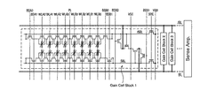
1つのセルブロックは、4個(多数個も可能)の直列接続されたメモリセルで構成されており、一端はプレート(/PLA,PLA)に接続されている。ここまでは先願と同じである。本実施形態においては、セルブロックの他端は、セルブロック選択トランジスタを介してサブビット線/SBLに接続されている。複数個のセルブロックが、サブビット線/SBLに接続されている。同様に、サブビット線SBL側にも複数個のセルブロックが接続されている。
【0224】
この図では、具体的に言うと4個のセルブロック、即ちWLA0〜WLA3をゲート、/PLAをプレート、BSA0をセルブロック選択信号とし、/SBLに接続される左上セルブロックと、WLA0〜WLA3をゲート、PLAをプレート、BSA1をセルブロック選択信号とし、SBLに接続される左下セルブロックと、WLB0〜WLB3をゲート、/PLBをプレート、BSB0をセルブロック選択信号とし、/SBLに接続される右上セルブロックと、WLB0〜WLB3をゲート、PLBをプレート、BSB1をセルブロック選択信号とし、SBLに接続される左上セルブロックとがある。
【0225】
トランジスタQ31は、サブビット線(/SBL)をゲート入力として、ソースをVSE電位に接続して、ドレインをビット線BLに接続しており、このトランジスタQ31を用いて/SBLの電位を増幅してビット線BLに伝える。トランジスタQ33は逆に、再書き込み時或いは書き込み時、ブロック書き込み選択信号BSX0をHighにして、ビット線/BLからの書き込み電位を、トランジスタQ33を介してサブビット線/SBLに伝え、セルにデータを再書き込みするのに用いている。
【0226】
トランジスタQ32は、サブビット線(SBL)をゲート入力として、ソースをVSE電位に接続して、ドレインをビット線/BLに接続しており、このトランジスタQ32を用いてSBLの電位を増幅してビット線/BLに伝える。トランジスタQ34は逆に、再書き込み時或いは書き込み時、ブロック書き込み選択信号BSX1をHighにして、ビット線BLからの書き込み電位を、トランジスタQ34を介してサブビット線SBLに伝え、セルにデータを再書き込みするのに用いている。
【0227】
トランジスタQ35,Q36は、サブビット線プリチャージ信号SBEをゲート入力として、サブビット線/SBL,SBLをある電位(VSB)にプリチャージするのに用いる。上記サブビット線と複数個のセルブロックと、増幅トランジスタ,ブロック書き込み選択トランジスタ,サブビット線プリチャージトランジスタを含むユニットを、ここではゲインセルブロックとする。
【0228】
ビット線対(/BL,BL)には、複数個の前記ゲインセルブロックが接続されている。この図の例では、3個までのゲインセルブロックが表示されているが、何個でも良い。そして、ビット線対(/BL,BL)は右端でセンスアンプ回路に接続されている。図87では省略してあるが、この図87の構成をワード線方向に複数個配置して、1つのセルアレイを構成する。
【0229】
本実施形態の特徴を簡単に言うと、図1はセルブロック内で自己増幅機能を有していたが、図87では、同じサブビット線に接続される複数のセルブロックで自己増幅機能を有して、これをさらに上の階層のビット線対に接続して、これをセンスアンプ回路に接続する構成を取る。従来FRAMが有効な領域よりは微細化が進み、図1が有効な領域ほどは微細化が進んでいなく、メモリセルの強誘電体キャパシタの分極量と比較して、セルブロック内の寄生容量が小さい場合有効であり、複数セルブロックが接続されるサブビット線を負荷容量として、セルデータを読み出し、これを増幅トランジスタで増幅して、ビット線に信号を読み出し、センスアンプで増幅する形態を取る。
【0230】
図88は、図87の具体的な動作例を示す信号波形図である。この動作図を参考に図87の動作,効果を説明する。図88は、セルトランジスタQ37と強誘電体キャパシタCF3で構成されるメモリセルのデータを読み出し、再書き込みする場合の動作例を示す。
【0231】
まずスタンドバイ時は、全てのワード線WLA0〜3,WLB0〜3は昇圧電位Vpp、全てのプレート線/PLA,PLA,/PLB,PLBは0V、セルブロック選択信号BSA0,BSA1,BSB0,BSB1は0V、セルトランジスタは全てONしており、全てのセルの強誘電体キャパシタの両端は電気的にショートされて、さらにセルブロック内のこれらセルキャパシタの両端の電位は、プレート線が0Vのため全て0Vになっている。また、ブロック書き込み選択信号は全て0Vにしておくことにより、トランジスタQ38,Q39はOFFしており、セルブロックとサブビット線は分離している。
【0232】
また、サブブロック選択プリチャージ信号SBEはHighにしてあり、サブビット線/SBL,SBLはVSBに接続され、ここではVSB=0Vに設定してあるので、サブビット線/SBL,SBLは0Vになっている。サブビット線/SBL,SBLが0V、VSEが0Vのため、増幅トランジスタQ31,Q32もOFFしているし、ブロック書き込み選択信号BSX0,BSX1も0Vになっているため、ブロック書き込み選択トランジスタQ33,Q34もOFFしている。よって、ビット線/BL,BLとサブビット線/SBL,SBLは完全に分離されている。
【0233】
ビット線/BL,BLは従来FRAMにおいては0Vにプリチャージする必要があったが、本発明においては、従来DRAMと同様に (1/2)VBLHにプリチャージすることができる。
【0234】
動作時は、選択したセルブロックの、例えば左上のセルブロックのメモリセル(Q37,CF3)選択時の動作を説明する。まず、選択メモリセルにつながるワード線WLA2を0Vに下げ、セルトランジスタQ37をOFFする。同時に或いは前後して、サブビット線を固定するサブブロック選択プリチャージ信号SBEを下げ、サブブロック選択プリチャージトランジスタQ35,Q36をOFFする。さらに、ビット線/BL,BLを (1/2)VBLHのままフローティングにする。
【0235】
ここで、その他のセルブロックのセルブロック選択トランジスタQ39,Q40,Q41はOFFしたままである。これにより、セルトランジスタQ37はOFF、Q38はON、サブビット線/SBLはフローティングであるため、選択したセルの強誘電体キャパシタCF3の右側の端子からセルブロック内、さらにサブビット線/SBLまでは全てつながり、かつ0Vでフローティングになる。
【0236】
次に、選択した左上のセルブロックに接続されるプレート/PLAのみを0Vから VBLH に上げる。PLAから選択した強誘電体キャパシタの左側端子まで VBLH 電位が印加される。このとき、CF3の右側の端子からセルブロック選択トランジスタまでと/SBLの容量が負荷容量CLとなり、強誘電体キャパシタに“1”データが書き込んであれば、分極反転して、セルデータがサブビット線/SBLに読み出され、/SBLの電位が0Vから2Vs+Voに上がる。強誘電体キャパシタに“0”データが書き込んであれば、分極反転せず、CF3の常誘電体成分容量とCLの容量比分だけ、サブビット線/SBLの電位上がり、/SBLの電位はVoとなる。
【0237】
このとき、対をなすサブビット線SBLの電位は、Q39,Q41がOFFのため、0Vのままである。ここで、VSE電位を0Vに設定しておくと、増幅トランジスタQ31のゲート電位は“1”データ時に2Vs+Vo、“0”データ時にVo、ソース電位(=VSE)は0V、ドレイン電位(=/BL)は (1/2)VBLHとなり、トランジスタQ31のしきい値電圧VtをVo<Vt<2Vs+Voに設計しておくと、図88に示すように、“1”データ時にトランジスタQ31はONしているため、 (1/2)VBLHにプリチャージされているBLは増幅トランジスタQ31を介して、VSEに電流が流れることにより、 (1/2)VBLHから電位が下がり始める。ここで、センスアンプ動作前の下がった電位を (1/2)VBLH−2Vstと定義する。
【0238】
逆に、“0”データ時、トランジスタQ31はOFFしているため、 (1/2)VBLHにプリチャージされているBLは増幅トランジスタQ31を介して、VSEに電流が流れず、 (1/2)VBLHのままである。このとき、定電流駆動トランジスタを用いたダミーセル等を用いて、/BL電位を“1”データ時BL側が下がる電位の半分の電位下げるように設定すると(即ちセンス動作前、(1/2)VBLH-Vst)、センスアンプ動作前、“1”データ時、BLは (1/2)VBLH−2Vst、/BLは (1/2)VBLH−VstとなりVstの電位差が図87の右端のセンスアンプに入力され、フリップフロップ型のセンスアンプで増幅され、BLは0V、/BLは VBLH となる。
【0239】
また、“0”データ時、BLは (1/2)VBLH、/BLは (1/2)VBLH−VstとなりVstの電位差が図87の右端のセンスアンプに入力され、フリップフロップ型のセンスアンプで増幅され、BLは VBLH 、/BLは0Vとなる。
【0240】
なお、上記増幅トランジスタのしきい値電圧は、Vt<Voの領域であった場合、/BLとBLの両方が増幅トランジスタがONして、/BL,BL電位が下がるわけであるが、この場合でも駆動電流に大きな違いがあり、ダミーセルの駆動電流を適切に設計すれば問題無い。また、VSEの電位は0Vでも良いし、しきい値の補正のため、ある一定の電位でも良い(即ち、VSEを0Vから上げた分だけ見かけ上増幅トランジスタのしきい値電圧を上げることができる)。
【0241】
データの再書き込み時、サブビット線/SBLに接続されるブロック書き込み制御信号BSX0のみVppに上げる。すると、0V或いは、 VBLH に増幅されたビット線/BLの電位が/SBLに書き込まれ、“1”データ時に/SBLは VBLH となり、“0”データ時に/SBLは0Vになる。このとき、プレート電位(=選択強誘電体キャパシタの左側の端子)は VBLH のため、“0”データ時、強誘電体キャパシタには−VBLHの電圧(強誘電体キャパシタの右側の端子を正と定義)が印加され、“0”データが再書き込みされる。“1”データ時は、その後、プレート/PLAが0Vに下げられ、選択強誘電体キャパシタの左側の端子も0Vになった時、強誘電体キャパシタには VBLH の電圧(強誘電体キャパシタの右側の端子を正と定義)が印加され、“1”データが再書き込みされる。
【0242】
これら一連の動作において、SBL電位はずっと0Vのままなので、下の左右セルブロックのデータは保持されたまま安定であるし、Q40もOFFしているため、右上のセルブロックのデータも安定である。例えば、外部から異なるデータを書き込む場合(ライト・モード)や、データの読み出し後に外部データを書き込む場合(リード・モディファイ・ライト)、BS0がHighになったあと書き込めば良い。
【0243】
再書き込み終了後は、まずブロック書き込み選択信号BSX0をHighから0Vに下げる。これにより、/BL側から/SBLへの干渉は無くなる。その後、WLA2を上げ、さらにセルブロック選択信号BSA0を下げると、選択されていたセルの強誘電体キャパシタは電気的にショートされ、全てのセルブロック内のノードは0Vになる。これら動作と同時に或いは前後して、ビット線対/BL、BLを電気的にショートしてやれば、ビット線対は (1/2)VBLHになり、SBEをHighに戻せば、サブビット線対も0Vにさがり、スタンドバイ状態に戻る。
【0244】
本実施形態においては、ビット線のプリチャージ電位を (1/2)VBLHにしているが、これができるのは、セル情報分極反転読み出すための負荷容量はサブビット線/SBL,SBLで行い、ビット線/BL,BLはセル情報分極反転読み出すための負荷容量では無いためである。このため、ビット対を電気的にショートするだけでプリチャージ電位である (1/2)VBLHが得られ、ビット線の充放電による消費電力を従来DRAM同様従来FRAMの半分に低減できるし、ビット線の充放電によるノイズを低減できる。
【0245】
以上、図87の回路図と図88の動作例で示したように、先願と同じように、強誘電体キャパシタとセルトランジスタを並列接続して、1セルとしてこれを複数直列接続して、これにブロック選択トランジスタを接続してセルブロックを構成することにより、4F2 サイズの高密度のセルを実現しつつ、平面トランジスタで製造の容易化を実現し、さらに高速なランダムアクセス機能を有することが可能となる。
【0246】
また、従来のFRAMにおいては、高密度化して設計ルールが縮小し、セルの強誘電体キャパシタ面積が設計ルールのほぼ2乗で縮小し、メモリセルの強誘電体キャパシタの分極量が減少するにも拘わらず、ビット線容量がそれほど減少しないため、読み出し信号量が減少して動作が困難になる問題点が合った。これに対し本実施形態では、サブビット線を増幅トランジスタのゲートに入力して、ドレイン端子をビット線に接続することにより、メモリセルの分極反転読み出しにより、セルブロックからサブビット線に読み出されたデータを増幅して、ビット線に伝えることができる。
【0247】
このとき、強誘電体キャパシタが分極反転するときの負荷容量CLは、CF3の右側の端子からセルブロック選択トランジスタまでとサブビット線/SBLの総計容量となり、サブビット線に接続されるセルブロック数を、先願のビット線に接続されるセルブロック数より少なくしてやれば、ビット線容量に比べて大幅に小さい値を取ることができ、強誘電体キャパシタサイズが小さくなっても、/SBLに読み出される信号量、即ち“1”データ時2Vs+Vo、“0”データ時Voの差の1/2であるVsの値は、大きな値を取ることが可能になる。これを増幅トランジスタQ31で増幅するため、いくらビット線/BL,BLの容量が大きくても安定動作が可能となる。
【0248】
例えば、サブビット線に接続されるセルブロック数を先願のビット線に接続されるセルブロック数の1/16にしてやれば、サブビット線の容量はほぼ1/16となり、強誘電体キャパシタの面積を1/16に縮小しても動作すると言うわけである。(正確には、セルブロック内の容量も含まれるため、1/16より大きい値となる、但し、この場合でも、ブロック数を1/32化等してやれば問題無い)。
【0249】
これは逆に言うと、本実施形態によれば、ビット線容量を増加しても、増幅トランジスタがビット線に読み出す信号を増幅するのに時間がかかるだけで、いくらでもビット線容量を増加できる。即ち、1本のビット線に接続されるゲインセルブロック数をいくらでも増加できるため、従来FRAMのような、チップ面積に占めるセンスアンプ面積が15%〜20%もある問題を解決して、ビット線に接続されるゲインセルブロック数を増加させ、センスアンプ数を減らし、センスアンプ面積のオーバヘッドをほとんど無くすることによりチップサイズを小さくする効果がある。
【0250】
本実施形態におけるセルブロック内部の負荷容量CLは、サブビット線に接続されるセルブロック数、セルブロックに直列接続されるセル数数の増減により変更が容易である。このことは、強誘電体キャパシタサイズが大きい時は、サブビット線に接続されるセルブロック数、セルブロックに直列接続されるセル数数を増加してCLを大きくして設計し、強誘電体キャパシタサイズが小さい時は、サブビット線に接続されるセルブロック数、セルブロックに直列接続されるセル数を減らしてCLを小さくして設計し、サブビット線に読み出される信号量を確保すれば良いことを示す。この2つのサブビット線に接続されるセルブロック数、セルブロックに直列接続されるセル数数のパラメータは独立して選択できる。
【0251】
この方式は、セルブロックに直列接続されるセルの容量+サブビット線の容量で負荷容量CLが決まるわけであり、図1のセルブロックに直列接続されるセルの容量に比べて、大きな値を取り得る。よって、図5に示したように、設計ルールが比較的緩いが、従来FRAMでは強誘電体キャパシタの分極量が不足するケースで有効である。例えば世代が進むに従って、ビット線に接続されるゲインセルブロック数を2,4,8,16,32,64と増やして行き、逆にサブビット線に接続されるセルブロック数を64,32,16,8,4,2と減らして行けば良い。
【0252】
このとき、選択したワード線の位置により、セル内の容量が変化して負荷容量CLも変化する問題があるため、サブビット線に接続されるセルブロック数が減った場合、セルブロック内のセル数も問題無い程度にへらした方が望ましい。即ち、サブビット線部容量/セルブロック内容量の比率を一定値以上に保つのが望ましい。例えば3以上の方が良い。また、図87と図1を組み合わせて、即ち図1の増幅トランジスタを無くし、ブロック書き込み選択トランジスタをブロック選択トランジスタとしたものをセルブロックとして、図87のような構成を取ると、負荷容量はブロックユニット内部容量+反対側のブロックユニット内部容量+サブビット線容量となり、より負荷容量が安定する。
【0253】
負荷容量CLが小さい場合、サブビット線に読み出される電位は確かに大きく確保できるが、総電荷量が小さいため、セルデータ読み出し時のサブビット線の拡散層に当るソフトエラーが問題となる。この問題に対して、上記直列セル数、サブビット線に接続されるセルブロック数の調整が有効であることは図1、図2、図4の説明から言うまでもない。即ち、設計ルールが緩く、ソフトエラーが厳しい状況では、これら数を増加させ負荷容量を追加してやれば、Qs=Vs×CLであり、多少Vsが減ってもQsが多くなり、より多くの反転電荷がサブビット線に読み出され、この問題はクリアできる。
【0254】
設計ルールが小さくなるに従って、ソフトエラーレートが下がるに従って、ソフトエラーが問題無い程度に、これら数を徐々に減らして、サブビット線に読み出される信号量を確保すれば、良いことが分かる。従来の自己増幅機能のあるメモリセルではこの調整をしようとすると、図237(d)のセルに限定される上、常誘電体キャパシタ面積が非常に大ききなり、コスト的に困難である。
【0255】
従来の自己増幅機能のあるメモリセルと比較すると、常誘電体キャパシタの大きな図237(d)のセルと同じ安定動作,正常動作を可能にしつつ、本実施形態によれば、1個のセルブロック内のセル数を増加するほど、1本のサブビット線に接続されるセルブロック数が増加するほど、複数のメモリセルで、前記増幅トランジスタと書き込みトランジスタを共用でき、セルサイズのオーバヘッドを極めて小さなものにできる。
【0256】
図87、図88の動作のもう1つの特徴は、セル信号により/SBLの電位が上がると、増幅トランジスタにより、ビット線対の反対側のBLの電位を下げる方式である。ビット線に読み出された信号をセンスアンプで増幅すると、/BL側を上げる結果となり、ブロック書き込み選択トランジスタを介して/SBL電位を正に上げるように再書き込みでき、つじつまが合う、この方式の場合、必ず増幅トランジスタのソース側がVSEとなり、サブビット線(/SBL,SBL)の電位がそのまま、ゲート−ソース間電位となり、ビット線の電位に拘わらず“1”データの場合増幅トランジスタが常にON、“0”データの場合常にOFFと制御し易いことが特徴である。
【0257】
言葉を変えると、ビット線電位が増幅され下がってもゲート−ソース間電位は一定であり、ドレイン−ソース電位が (1/2)VBLHと大きく5極管動作であり、定電流駆動であるため、ダミーセルが製造し易いことを意味する。もちろん図87の回路は1セルに1個の情報を記憶する1トランジスタ+1キャパシタ方式であるが、2セルに1個の情報を記憶する2トランジスタ+2キャパシタ方式が動作を変えるだけで実現できる。
【0258】
これは図88において、/PLAばかりでなくPLAも駆動して、BS0ばかりでなくBS1もLow→High→Lowと駆動すれば容易に実現できる。例えば、1トランジスタ+1キャパシタ方式でテストを行い、欠陥セルをスクリーニングして、リダンダンシーで置換え、実際の製品としては、信頼性の高い2トランジスタ+2キャパシタ方式で動作させる方法とかがこれに当てはまる。
【0259】
また本実施形態によれは、図88に示すように、従来FRAMに比べて、ブロック書き込み制御信号をセル読み出し後にクロッキングするオーバヘッド以外は動作が遅くなる要因が無く、高速動作が期待できる。本方式おいて、WLA0を下げるタイミングとビット線及びサブビット線のイコライズを解除するタイミングが同時に行えるメリットを考慮すると、上のオーバヘッドは相殺できる。
【0260】
また従来FRAMは、各セル毎にプレートを分離する必要がある上、プレートの強誘電体キャパシタの負荷が大きい点、プレート抵抗が大きい点、プレートドライバサイズを大きくできない(大きくすると、ワード線1本毎にプレートドライバがあるためチップサイズ増)ためドライバの駆動能力低い等、プレート動作が遅い問題点が合った。これに対し本実施形態は先願を同じく、プレートドライバが複数のワード線で共有でき、駆動能力大、プレート線が本数が少ないため、メタル配線にしたり配線幅が大きくできたりと抵抗成分が小さい上、負荷容量は殆ど強誘電体キャパシタ容量で決まるため変わらず、結果として高速プレート駆動が可能となる。
【0261】
以上、図87と図88の効果をまとめると、
1)先願と同様に、4F2 サイズの高密度のセルを実現しつつ、平面トランジスタで製造の容易化を実現し、さらに高速なランダムアクセス機能を有することが可能。
【0262】
2)設計ルールが縮小して、強誘電体キャパシタ面積が縮小しても、それに合わせて分極反転時の負荷容量であるサブビット線容量が低減でき、十分な読み出し信号電圧が得られ、増幅トランジスタを用いてビット線を増幅するため、安定動作が可能。
【0263】
3) (1/2)Vdd(=VBLH)ビット線プリチャージが適用でき、低消費電力,低ノイズ。
4)従来FRAMと同様動作原理が単純で、しかも高速プレート動作により高速動作が可能。
【0264】
5)ビット線容量が大きくても読み出し可能であるため、ビット線に接続できるセルブロック数を多くでき、結果としてセンスアンプ面積を低減できる。
6)ルール縮小により、強誘電体キャパシタの分極量の減少に合わせて、セルブロック内の直列セル数や、サブビット線に接続されるセルブロック数を減らせば、最適化が可能。
【0265】
7)設計ルールが緩く、ソフトエラーが厳しい状況では、セルブロックの直列セル数や、サブビット線に接続されるセルブロック数を増加させ、負荷容量を追加して読み出し電荷を増やせば、ソフトエラーを抑えられ、設計ルールが小さくなるに従って、ソフトエラーレートが下がるに従って、ソフトエラーが問題無い程度に、強誘電体キャパシタサイズと、直列セル数や、サブビット線に接続されるセルブロック数を徐々に減らして、サブビット線に読み出される信号量を確保すれば良い。
【0266】
8)複数のセルブロックで、増幅トランジスタと、書き込みトランジスタ、サブビット線選択プリチャージトランジスタを共用することにより、セルサイズのオーバヘッドを極めて小さなものにできる。
【0267】
9)分極反転の為の負荷容量として、サブビット線の容量を利用でき、ほぼ安定に動作が可能。
10)セルブロックのセル数、サブビット線に接続されるセルブロック数を変えることにより、自由に負荷容量の調整が可能。
【0268】
11)サブビット線の信号でビット線対の反対側のビット線を増幅トランジスタで駆動することにより安定な増幅動作が可能となる。
12)サブビット線の寄生容量が負荷容量となりうるため、セルブロック内の寄生容量だけでは、負荷容量が不足な、微細化が進んでいるがそれほどでは無い領域から、従来のFRAM構成では、僅かにメモリセルの強誘電体キャパシタの分極量が不足する領域までの広いレンジをカバー可能である。
【0269】
図89〜図91は、図87の具体的な別の動作例を示す信号波形図である。いずれも、図87のゲインセルブロック構成で、図9のセンスアンプ回路を用いた場合の動作波形例を示している。図89は図12(b)のキャパシタカップリング型ダミーセルを用いた場合を示し、図90は図16(a)の定電流型ダミーセルを用いた場合を示し、図91は図16(b)の定電流型ダミーセルを用いた場合を示す。もちろん図87の構成でも、固定のサブビット線容量に選択したワード線の位置により変化するセルブロック内容量を持つため、負荷容量は多少変化する。よってもちろん、図12(c)、図16(c)タイプのダミーセルが可能だし、図87をベースに改良したメモリセルを用いるダミーセルも可能である。
【0270】
(第29の実施形態)
図92は、本発明の第29の実施形態に係わる半導体記憶装置を示す回路構成図であり、特に強誘電体メモリのブロック構成を示している。図93は、図92の具体的な動作例を示す信号波形図である。
【0271】
図92は、図87とほぼ同一の構成であり、殆どの効果が図87と同じである。異なる点は、サブビット線/SBLをゲート入力とする増幅トランジスタのソースがビット線/BL側に接続され、ドレインがVSE電位に接続される。サブビット線SBLをゲート入力とする増幅トランジスタのソースがビット線BL側に接続され、ドレインがVSE電位に接続される点である。即ち、読み出すビット線と、書き込みを行うビット線が同じビット線/BL或はBLである点である。
【0272】
図93の動作では、VSEがビット線プリチャージ電圧より高く設定されており、増幅トランジスタにより、増幅トランジスタがON時、ビット線が上に増幅して上がることが分かる。ビット線対はVssプリチャージが望ましいが、Vt設定により図93のような (1/2)VBLHプリチャージ方式が適用できる。
【0273】
(第30の実施形態)
図94は、本発明の第30の実施形態に係わる半導体記憶装置を示す回路構成図であり、特に強誘電体メモリのブロック構成を示している。図95は、図94の具体的な動作例を示す信号波形図である。
【0274】
図94は図87とほぼ同一の構成であり、殆どの効果が図87と同じである。異なる点は、図87の左上下のセルブロックをワード線方向を軸に折り返し、右上下のセルブロックをワード線方向を軸に折り返している点である。これにより、左上下のセルブロックと右上下のセルブロックの2種類のプレート線を共有できるメリットがあることが分かる。なお、図87の例でも4個以上のセルブロックを同じサブビット線に接続する場合も同様にプレートは共有できる。
【0275】
図95は、図94の具体的動作例を示す。プレートが共有されて動作している点を除けば動作は図88と同じである。
【0276】
(第31の実施形態)
図96は、本発明の第31の実施形態に係わる半導体記憶装置を示す回路構成図であり、特に強誘電体メモリのブロック構成を示している。図97は、図96の具体的な動作例を示す信号波形図である。
【0277】
図96と図97は、図92と図93の回路及び動作で、図94及び95と同様にセルブロックを折り返した場合を示す。
【0278】
(第32の実施形態)
図98は、本発明の第32の実施形態に係わる半導体記憶装置を示す回路構成図である。図98は図87とほぼ同様の構成であり、殆どの効果が図87と同じである。異なる点は、図87では上のセルブロックと下のセルブロックで、ブロック選択信号を2種類に分けていたが、図98においては1種類のブロック選択信号(BSA,BSB)で制御している。
【0279】
図99は、図98の具体的な動作例を示す信号波形図である。図99の動作のように、例えばWLA2を上げ、BSAを上げ、/PLAを上げて、左上のセルブロックのセルをサブビット線に読み出す場合、ブロック選択信号を共有したため、サブビット線と左下のセルブロックの内部ノードは接続される。しかし、スタンドバイ時、サブビット線SBLを0Vにプリチャージ、プレート線PLAを0V設定しておけば、サブビット線と左下のセルブロックの内部ノードが接続されても、アクティブ時にPLAは0Vのままで、セルブロックの内部ノードは0Vのままで、サブビット線SBLを0Vのままのため問題が起こらない。
【0280】
(第33の実施形態)
図100は、本発明の第33の実施形態に係わる半導体記憶装置を示す回路構成図であり、特に強誘電体メモリのブロック構成を示している。図101は、図100の具体的な動作例を示す信号波形図である。
【0281】
図100の回路と図101の動作は、図98と図99とほぼ同一の構成であり、殆どの効果が図98及び図99と同じである。異なる点は、サブビット線からデータの読み出しをするビット線とサブビット線に書き込むビット線が同じ点である。
【0282】
(第34の実施形態)
図102は、本発明の第34の実施形態に係わる半導体記憶装置を示す回路構成図であり、特に強誘電体メモリのブロック構成を示している。図103は、図102の具体的な動作例を示す信号波形図である。
【0283】
図102の回路と図103の動作は、図98及び図99とほぼ同一であり、殆どの効果は図98及び図99と同じである。異なる点は、図94及び図95と同様にセルブロックを折り返し、プレートを共有化した点である。
【0284】
(第35の実施形態)
図104は、本発明の第35の実施形態に係わる半導体記憶装置を示す回路構成図であり、特に強誘電体メモリのブロック構成を示している。図105は、図104の具体的な動作例を示す信号波形図である。
【0285】
図104の回路と図105の動作は、図102及び図103とほぼ同一であり、殆どの効果が図102及び図103と同じである。異なる点は、サブビット線からデータの読み出しをするビット線とサブビット線に書き込むビット線が同じ点である。
【0286】
(第36の実施形態)
図106は、本発明の第36の実施形態に係わる半導体記憶装置を示す回路構成図であり、特に強誘電体メモリのブロック構成を示している。
【0287】
図106は図87とほぼ同一の構成であり、殆どの効果は図87と同じである。異なる点は、フォールデッドBL構成でプレート駆動読み出し・書き込みを行うため、図87ではプレート線をサブビット線/SBL,SBLに対応して2種類のプレート線を用いていたのに対し、図106においてはプレート線を1種類にして、即ち上のセルブロックと下のセルブロックで同じプレート線を用いている点である。
【0288】
図107は、図106の具体的な動作例を示す信号波形図である。図106の方式では (1/2)Vdd(=(1/2)VBLH)固定プレート動作が可能となる。アクティブ時、プレート線をVPL(=(1/2)VBLH)に固定にしたまま、ワード線WLA2を下げ、ブロック選択トランジスタ信号BSA0を上げると、サブビット線/SBLが0Vにプリチャージされているため、左上のセルブロックの選択したセルの強誘電体キャパシタに自動的に (1/2)VBLHの電圧が印加され、セルデータがサブビット線/SBLに読み出される。その後の動作は図87と同じである。
【0289】
図87と異なる点は、データ再書き込み時、サブビット線/SBLが0V或いはVBLHにフル振幅されると、プレート線が (1/2)VBLHのため、自動的に+(1/2)VBLH 或いは−(1/2)VBLH の電位が強誘電体キャパシタに印加されるため、データの再書き込みが可能となる。結局プレート固定のままで、データの読み出し,書き込みができる。この動作の時、左下のセルブロックのWLA2に接続されるメモリセルトランジスタもOFFして、このトランジスタからブロック選択トランジスタまでがフローティングになるが、プレートを駆動しないため、 (1/2)VBLH電位でフローティングになっているだけで問題無い。
【0290】
このアクティブ時のフローティングはpn接合リーク等でこのノードの電位が下がってしまう問題を抱えるが、通常のDRAM,FRAM等のアクティブ時間は最大10μsと規定されており、リークが問題となる256ms等の最大リフレッシュ時間に比べて桁が小さいので問題無いことが判る。
【0291】
(第37の実施形態)
図108は、本発明の第37の実施形態に係わる半導体記憶装置を示す回路構成図であり、特に強誘電体メモリのブロック構成を示している。図109は、図108の具体的な動作例を示す信号波形図である。
【0292】
図108の回路と図109の動作は、図106及び図107とほぼ同一であり、殆どの効果は図106及び図107と同じである。異なる点は、サブビット線からデータの読み出しをするビット線とサブビット線に書き込むビット線が同じ点である。
【0293】
(第38の実施形態)
図110及び図111は、本発明の第38の実施形態に係わる半導体記憶装置を示す回路構成図であり、特に強誘電体メモリのブロック構成を示している。
【0294】
図110の回路は、図106とほぼ同一の構成であり、殆どの効果は図106と同じである。異なる点は、セルブロックを折り返し、プレートを共有化した点である。
【0295】
図111の回路は、図98とほぼ同一の構成であり、ほとんどの効果が図98と同じである。異なる点は、セルブロックを折り返し、プレートを共有化した点である。
【0296】
(第39の実施形態)
図112は、本発明の第39の実施形態に係わる半導体記憶装置を説明するための平面図であり、特に強誘電体メモリのゲインセルブロック構成のレイアウトを示している。図112(a)は図94の配置位置のトポロジも対応したレイアウト図を示し、図112(b)は図102の配置位置のトポロジも対応したレイアウト図を示し、図112(c)は図110の配置位置のトポロジも対応したレイアウト図を示す。複数層重ねると判りにくいため、同じレイアウトの各層を図113から図116に分けて表示してある。
【0297】
図113(a)〜(c)は図112のレイアウトの一部の層のレイアウトに対応し、図114(a)〜(c)は図112のレイアウトの一部の層のレイアウトに対応し、図115(a)〜(c)は図112のレイアウトの一部の層のレイアウトに対応し、図116(a)〜(c)は図112のレイアウトの一部の層のレイアウトに対応している。
【0298】
各レイヤ表示として、拡散層をAA、ゲート層をGC、上部電極層をTE、下部電極層をBE、強誘電体層をFE、サブビット線層をSBL、ビット線層をBL、拡散層−下部電極層間コンタクトをAA−BE−C、拡散層−上部電極層間コンタクトをAA−TE−C、ゲート層−下部電極層間コンタクトをGC−BE−C、上部電極層−ビット線層間コンタクトをTE−BL−C、下部電極−サブビット線層間コンタクトをBE−SBL−C、上部電極−サブビット線層間コンタクトをTE−SBL−C、サブビット線−ビット線間コンタクトをSBL−BL−Cと定義している。
【0299】
上部電極層及び下部電極層は、強誘電体キャパシタの上下電極層を意味する。図28の配線構成に対して、サブビット線層を1層追加した構成になっており、僅か1層の配線層の追加で、図87〜図111の構成が実現できている。また、セルアレイ内でピッチが厳しいにも拘わらず、無理なく自己増幅機能を実現するトランジスタが配置できている。
【0300】
(第40の実施形態)
図117は、本発明の第40の実施形態に係わる半導体記憶装置を説明するための素子構造断面図であり、特に強誘電体メモリのゲインセルブロック構成を示している。図117は、図112(b)のレイアウト構成の断面図に対応していて、図117の(a),(b),(c)は、ビット線方向で/BL中央,/BLとBLの中間,BL中央で割った時の断面図に対応する。BEを巧みに用いることによりコンパクトで、設計余裕がありつつ自己増幅機能を実現していることが判る。
【0301】
(第41の実施形態)
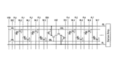
図118は、本発明の第41の実施形態に係わる半導体記憶装置を示す回路構成図であり、特に強誘電体メモリのゲインセルブロック構成を示している。
【0302】
従来の1トランジスタ+1キャパシタ型の強誘電体メモリと同様に、1個のメモリセルは、セルトランジスタと強誘電体キャパシタの直列接続で構成され、セルトランジスタのゲートは、ワード線WL0〜WL7に接続される。強誘電体キャパシタの他端はプレート電極(PL0〜PL7)に接続されている。
【0303】
ここまでは従来FRAMと同じである。本実施形態においては、セルトランジスタの他端は、サブビット線/SBLに接続されている。複数個のセルが、サブビット線/SBLに接続されている。同様に、サブビット線SBL側にも複数個のセルが接続されている。この図では具体的に言うと、/SBLに4個のメモリセル、SBLに4個のメモリセルが接続されている。各メモリセルのプレート電極は各々分離されている(PL0〜PL7)。
【0304】
トランジスタQ42は、サブビット線(/SBL)をゲート入力として、ソースをVSE電位に接続して、ドレインをビット線BLに接続しており、このトランジスタQ42を用いて/SBLの電位を増幅してビット線BLに伝える。トランジスタQ45は逆に、再書き込み時、あるいは書き込み時、ブロック書き込み選択信号BS0をHighにして、ビット線/BLからの書き込み電位を、トランジスタQ45を介してサブビット線/SBLに伝え、セルにデータを再書き込みするのに用いている。
【0305】
トランジスタQ43は、サブビット線(SBL)をゲート入力として、ソースをVSE電位に接続して、ドレインをビット線/BLに接続しており、このトランジスタQ43を用いてSBLの電位を増幅してビット線/BLに伝える。トランジスタQ46は逆に、再書き込み時或いは書き込み時、ブロック書き込み選択信号BS1をHighにして、ビット線BLからの書き込み電位を、トランジスタQ46を介してサブビット線SBLに伝え、セルにデータを再書き込みするのに用いている。
【0306】
トランジスタQ47,Q48は、サブビット線プリチャージ信号SBEをゲート入力として、サブビット線/SBL,SBLをある電位(VSB)にプリチャージするのに用いる。上記、サブビット線と複数個のセルブロックと、増幅トランジスタ,ブロック書き込み選択トランジスタ,サブビット線プリチャージトランジスタを含むユニットを、ここではゲインセルブロックとする。ビット線対(/BL,BL)には、複数個の前記ゲインセルブロックが接続されている。この数は設計により何個でも良い。そして、ビット線対(/BL,BL)の一端でセンスアンプ回路に接続されている。
【0307】
本実施形態の特徴を簡単に言うと、図118では、同じサブビット線に接続される複数のセルで自己増幅機能を有して、これをさらに上の階層のビット線対に接続して、これをセンスアンプ回路に接続する構成を取っている、これにより、従来FRAMでは、微細化が進み、メモリセルの強誘電体キャパシタの分極量が減少して、セル読み出し信号量が確保できない時代になったとしても、従来FRAMのビット線に接続されるセル数より、本実施形態のサブビット線に接続されるセル数を少なく設定すれば、軽いサブビット線を負荷容量として、セルデータを読み出すため、十分なサブビットへの読み出し信号量が確保できる。これを増幅トランジスタで増幅して、ビット線に信号を読み出し、センスアンプで増幅する形態を取る。
【0308】
図119は、図118の具体的な動作例を示す信号波形図である。この動作図を参考に図118の動作及び効果を説明する。図119は、セルトランジスタQ49と強誘電体キャパシタCF4で構成されるメモリセルのデータを読み出し、再書き込みする場合の動作例を示す。
【0309】
まずスタンドバイ時は、全てのワード線WL0〜7は0Vでセルトランジスタは全てOFFしており、全てのプレート線PL0〜PL7は0V、またブロック書き込み選択信号BS0,BS1は全て0Vにしてある。また、サブブロック選択プリチャージ信号SBEはHighにしてあり、サブビット線/SBL,SBLはVSBに接続され、ここではVSB=0Vに設定してあるので、サブビット線/SBL,SBLは0Vになっている。サブビット線/SBL,SBLが0V、VSEが0Vのため、増幅トランジスタQ42,Q43もOFFしているし、ブロック書き込み選択信号BS0,BS1も0Vになっているため、ブロック書き込み選択トランジスタQ45,Q46もOFFしている。
【0310】
よって、ビット線/BL,BLとサブビット線/SBL,SBLは完全に分離されている。ビット線/BL,BLは従来FRAMにおいては、0Vにプリチャージする必要があったが、本実施形態においては従来DRAMと同様に、(1/2)VBLHにプリチャージすることができる。
【0311】
メモリセル(Q49,CF4)選択時の動作を説明する。まず、サブビット線を固定するサブブロック選択プリチャージ信号SBEを下げ、サブブロック選択プリチャージトランジスタQ47,Q48をOFFする。本実施形態では、サブビット線の両側にこのサブブロック選択プリチャージトランジスタQ47,Q48が配置されている。さらに、ビット線/BL,BLを (1/2)VBLHのままフローティングにする。
【0312】
次に、ワード線WL0をVppに上げ、セルトランジスタQ49をONする。次に、選択したセルに対応するプレート線PL0を0Vから VBLH に上げる。このとき、複数のセルが接続されるサブビット線/SBLの容量が負荷容量CLとなり、強誘電体キャパシタに“1”データが書き込んであれば、分極反転して、セルデータがサブビット線/SBLに読み出され/SBLの電位が0Vから2Vs+Voに上がる。強誘電体キャパシタに“0”データが書き込んであれば、分極反転せず、CF4の常誘電体成分容量とCLの容量比分だけ、サブビット線/SBLの電位上がり、/SBLの電位はVoとなる。
【0313】
このとき、対をなすサブビット線SBLの電位は、これに接続される全てのセルトランジスタがOFFであり、ブロック書き込み選択信号BS1も0Vになっているため0Vのままである。ここで、VSE電位を0Vに設定しておくと、増幅トランジスタQ42のゲート電位は“1”データ時に2Vs+Vo、“0”データ時にVo、ソース電位(=VSE)は0V、ドレイン電位(=/BL)は (1/2)VBLHとなる。
【0314】
そして、トランジスタQ42のしきい値電圧VtをVo<Vt<2Vs+Voに設計しておくと、図119に示すように、“1”データ時、トランジスタQ42はONしているため、 (1/2)VBLHにプリチャージされているBLは増幅トランジスタQ42を介して、VSEに電流が流れることにより、 (1/2)VBLHから電位が下がり始める。ここで、センスアンプ動作前の下がった電位を (1/2)VBLH−2Vstと定義する。逆に、“0”データ時、トランジスタQ42はOFFしているため、 (1/2)VBLHにプリチャージされているBLは増幅トランジスタQ42を介して、VSEに電流が流れず、 (1/2)VBLHのままである。
【0315】
このとき、定電流駆動トランジスタを用いたダミーセル等を用いて、/BL電位を“1”データ時BL側が下がる電位の半分の電位下げるように設定すると(即ちセンス動作前、(1/2)VBLH-Vst)、センスアンプ動作前、“1”データ時、BLは (1/2)VBLH−2Vst、/BLは (1/2)VBLH−VstとなりVstの電位差が図118の右端のセンスアンプに入力され、フリップフロップ型のセンスアンプで増幅され、BLは0V、/BLは VBLH となる。また、“0”データ時、BLは (1/2)VBLH、/BLは (1/2)VBLH−VstとなりVstの電位差が図118の右端のセンスアンプに入力され、フリップフロップ型のセンスアンプで増幅され、BLは VBLH 、/BLは0Vとなる。
【0316】
なお、上記増幅トランジスタのしきい値電圧は、Vt<Voの領域であった場合、/BLとBLの両方が増幅トランジスタがONして、/BL,BL電位が下がるわけであるが、この場合でも駆動電流に大きな違いがあり、ダミーセルの駆動電流を適切に設計すれば問題無い。また、VSEの電位は0Vでも良いし、しきい値の補正のため、ある一定の電位でも良い(即ち、VSEを0Vから上げた分見かけ上増幅トランジスタのしきい値電圧を上げることができる)。
【0317】
データの再書き込み時、サブビット線/SBLに接続されるブロック書き込み制御信号BS0のみVppに上げる。すると、0V或いは VBLH に増幅されたビット線/BLの電位が/SBLに書き込まれ、“1”データ時に/SBLは VBLH となり、“0”データ時に/SBLは0Vになる。このとき、プレート線(PL0)は VBLH のため、“0”データ時、強誘電体キャパシタには−VBLHの電圧(強誘電体キャパシタの右側の端子を正と定義)が印加され、“0”データが再書き込みされる。“1”データ時は、その後、プレートPL0が0Vに下げられ、強誘電体キャパシタには VBLH の電圧(強誘電体キャパシタの右側の端子を正と定義)が印加され、“1”データが再書き込みされる。
【0318】
これら一連の動作において、SBL電位はずっと0Vのままなので、下の左右セルブロックのデータは保持されたまま、安定である。例えば、外部から異なるデータを書き込む場合(ライト・モード)や、データの読み出し後外部データを書き込む場合(リード・モディファイ・ライト)、BS0がHighになったあと書き込めば良い。再書き込み終了後は、まずブロック書き込み選択信号BS0をHighから0Vに下げる。これにより、/BL側から/SBLへの干渉は無くなる。その後、WL0を下げるとセルデータは保持される。その後、ビット線対/BL,BLを電気的にショートしてやれば、ビット線対は (1/2)VBLHになり、SBEをHighに戻せば、サブビット線対も0Vに下がり、スタンドバイ状態に戻る。
【0319】
本実施形態においては、ビット線のプリチャージ電位を (1/2)VBLHにしているが、これができるのは、セル情報分極反転読み出すための負荷容量はサブビット線/SBL,SBLで行い、ビット線/BL,BLはセル情報分極反転読み出すための負荷容量では無いためである。このため、ビット対を電気的にショートするだけでプリチャージ電位である (1/2)VBLHが得られ、ビット線の充放電による消費電力を従来DRAM同様に従来FRAMの半分に低減できるし、ビット線の充放電によるノイズを低減できる。
【0320】
以上、図118の回路図と図119の動作例で示したように、従来FRAMと同じメモリセルを用いるため、DRAMと同様な高密度化がはかれる。さらに、従来のFRAMにおいては、高密度化して設計ルールが縮小し、セルの強誘電体キャパシタ面積が設計ルールのほぼ2乗で縮小し、メモリセルの強誘電体キャパシタの分極量が減少するにも拘わらず、ビット線容量がそれほど減少しないため読み出し信号量が減少して、動作が困難になる問題点があつた。
【0321】
これに対し本実施形態では、サブビット線を増幅トランジスタのゲートに入力して、ドレイン端子をビット線に接続することにより、メモリセルの分極反転読み出しにより、セルブロックから、サブビット線に読み出されたデータを増幅して、ビット線に伝えることができる。このとき、強誘電体キャパシタが分極反転するときの負荷容量CLは、サブビット線/SBLの容量となり、サブビット線に接続されるセル数を、先願のビット線に接続されるセルブロック数より少なくしてやれば、ビット線容量に比べて大幅に小さい値を取ることができる。
【0322】
そして、強誘電体キャパシタサイズが小さくなっても、/SBLに読み出される信号量、即ち“1”データ時2Vs+Vo、“0”データ時Voの差の1/2であるVsの値は、大きな値を取ることが可能になる。これを増幅トランジスタQ42で増幅するため、いくらビット線/BL,BLの容量が大きくても安定動作が可能となる。
【0323】
例えば、サブビット線に接続されるセルブロック数を先願のビット線に接続されるセルブロック数の1/16にしてやれば、サブビット線の容量はほぼ1/16となり、強誘電体キャパシタの面積を1/16に縮小しても動作すると言うわけである。これは逆に言うと本実施形態によれば、ビット線容量を増加しても、増幅トランジスタがビット線に読み出す信号を増幅するのに時間がかかるだけで、いくらでもビット線容量を増加できる。
【0324】
即ち、1本のビット線に接続されるゲインセルブロック数をいくらでも増加できるため、従来FRAMのような、チップ面積に占めるセンスアンプ面積が15〜20%もある問題を解決して、ビット線に接続されるゲインセルブロック数を増加させ、センスアンプ数を減らし、センスアンプ面積のオーバヘッドを殆ど無くすることによりチップサイズを小さくする効果がある。
【0325】
本実施形態におけるセルブロック内部の負荷容量CLは、サブビット線に接続されるセル数の増減により変更が容易である。このことは、強誘電体キャパシタサイズが大きい時は、サブビット線に接続されるセル数を大きくして設計し、強誘電体キャパシタサイズが小さい時は、サブビット線に接続されるセル数を減らしてCLを小さくして設計し、サブビット線に読み出される信号量を確保すれば良いことを示す。よって、図5に示したように、設計ルールが比較的緩いが、従来FRAMでは、強誘電体キャパシタの分極量が不足するケースで有効である。例えば世代が進みに従って、ビット線に接続されるゲインセルブロック数を2,4,8,16,32,64と増やして行き、逆にサブビット線に接続されるセル数を512,256,128,64,32,16,8と減らして行けば良い。
【0326】
このとき、選択したワード線の位置により、セル内の容量が変化して負荷容量CLも変化する問題はこの発明では存在しない。負荷容量CLが小さい場合、サブビット線に読み出される電位は確かに大きく確保できるが、総電荷量が小さいため、セルデータ読み出し時のサブビット線の拡散層に当るソフトエラーが問題となる。この問題に対して、上記サブビット線に接続されるセル数の調整が有効であることは図4の説明から言うまでもない。即ち、設計ルールが緩く、ソフトエラーが厳しい状況では、これら数を増加させ、負荷容量を追加してやれば、Qs=Vs×CLであり、多少Vsが減っても、Qsが多くなり、より多くの反転電荷がサブビット線に読み出され、この問題はクリアできる。
【0327】
設計ルールが小さくなるに従って、ソフトエラーレートが下がるに従って、ソフトエラーが問題無い程度に、これら数を徐々に減らして、サブビット線に読み出される信号量を確保すれば、良いことが分かる。従来の自己増幅機能のあるメモリセルではこの調整をしようとすると、図237(d)のセルに限定される上、常誘電体キャパシタ面積が非常に大ききなり、コスト的に困難である。
【0328】
従来の自己増幅機能のあるメモリセルと比較すると、常誘電体キャパシタの大きな図237(d)のセルと同じ安定動作,正常動作を可能にしつつ、本実施形態によれば、1本のサブビット線に接続されるセルブロック数が増加するほど、複数のメモリセルで、前記増幅トランジスタと書き込みトランジスタ及びサブブロック選択プリチャージトランジスタを共用でき、セルサイズのオーバヘッドを極めて小さなものにできる。
【0329】
図118と図119の動作のもう1つの特徴は、セル信号により/SBLの電位が上がると、増幅トランジスタによりビット線対の反対側のBLの電位を下げる方式である。ビット線に読み出された信号をセンスアンプで増幅すると、/BL側を上げる結果となり、ブロック書き込み選択トランジスタを介して/SBL電位を正に上げるように、再書き込みでき、つじつまが合う、この方式の場合、必ず増幅トランジスタのソース側がVSEとなり、サブビット線(/SBL,SBL)の電位がそのまま、ゲート−ソース間電位となり、ビット線の電位に拘わらず、“1”データの場合増幅トランジスタが常にON、“0”データの場合常にOFFと制御し易いことが特徴である。
【0330】
言葉を変えると、ビット線電位が増幅され下がってもゲート−ソース間電位は一定であり、ドレイン−ソース電位が (1/2)VBLHと大きく、5極管動作であり,定電流駆動であるため、ダミーセルが製造し易いことを意味する。もちろん図118の回路は1セルに1個の情報を記憶する1トランジスタ+1キャパシタ方式であるが、2セルに1個の情報を記憶する2トランジスタ+2キャパシタ方式が動作を変えるだけで実現できる。
【0331】
これは図119において、PL0ばかりでなくPL1も駆動して、BS0ばかりでなくBS1もLow→High→Lowと駆動すれば容易に実現できる。例えば、1トランジスタ+1キャパシタ方式でテストを行い、欠陥セルをスクリーニングして、リダンダンシーで置換え、実際の製品としては、信頼性の高い2トランジスタ+2キャパシタ方式で動作させる方法とかがこれに当てはまる。
【0332】
また本実施形態によれは、図119に示すように、従来FRAMに比べて、ブロック書き込み制御信号をセル読み出し後にクロッキングするオーバヘッド以外は動作が遅くなる要因が無く、高速動作が期待できる。むしろ自己増幅機能により、ある一定の信号値がビット線に読み出される速度が速くなり、上記ペナルティを克服できる。
【0333】
以上、図118と図119の効果をまとめると、
1)従来FRAMと同様に8F2 サイズの高密度のセルを実現しつつ、平面トランジスタで製造の容易化を実現し、さらに高速なランダムアクセス機能を有することが可能。
【0334】
2)設計ルールが縮小して、強誘電体キャパシタ面積が縮小しても、それに合わせて分極反転時の負荷容量であるサブビット線容量が低減でき、十分な読み出し信号電圧が得られ、増幅トランジスタを用いてビット線を増幅するため、安定動作が可能。
【0335】
3) (1/2)Vdd(=VBLH)ビット線プリチャージが適用でき、低消費電力,低ノイズ。
【0336】
4)従来FRAMと同様に、動作原理が単純である。
【0337】
5)ビット線容量が大きくても読み出し可能であるため、ビット線に接続できるゲインセルブロック数を多くでき、その結果としてセンスアンプ面積を低減できる。
【0338】
6)ルール縮小により、強誘電体キャパシタの分極量の減少に合わせて、サブビット線に接続されるセル数を減らせば、最適化が可能。
【0339】
7)設計ルールが緩く、ソフトエラーが厳しい状況では、サブビット線に接続されるセル数を増加させ、負荷容量を追加して読み出し電荷を増やせば、ソフトエラーを抑えられ、設計ルールが小さくなるに従って、ソフトエラーレートが下がるに従って、ソフトエラーが問題無い程度に、強誘電体キャパシタサイズと、サブビット線に接続されるセル数を徐々に減らして、サブビット線に読み出される信号量を確保すれば良い。
【0340】
8)複数のセルで、増幅トランジスタ,書き込みトランジスタ,サブビット線選択プリチャージトランジスタを共用することにより、セルサイズのオーバヘッドを極めて小さなものにできる。
【0341】
9)分極反転のための負荷容量として、サブビット線の容量を利用でき、ほぼ安定に動作が可能。
【0342】
10)サブビット線に接続されるセル数を変えることにより、自由に負荷容量の調整が可能。
【0343】
11)サブビット線の信号でビット線対の反対側のビット線を増幅トランジスタで駆動することにより、安定な増幅動作が可能となる。
【0344】
12)サブビット線の寄生容量が負荷容量となりうるため、微細化が進んで、完全に強誘電体キャパシタの分極量が小さいく不足する領域から、従来のFRAM構成では、僅かにメモリセルの強誘電体キャパシタの分極量が不足する領域までの広いレンジをカバー可能である。
【0345】
(第42の実施形態)
図120は、本発明の第42の実施形態に係わる半導体記憶装置を示す回路構成図であり、特に強誘電体メモリのゲインセルブロック構成を示している。
【0346】
図120は図118と同様な構成を取り同様な効果を持つが、異なる点は、図118ではサブビット線の両側にサブブロック選択プリチャージトランジスタを配置していたが、図120では一端のみに配置して、面積を低減していることである。動作法は、図119と同一である。
【0347】
(第43の実施形態)
図121は、本発明の第43の実施形態に係わる半導体記憶装置を示す回路構成図であり、特に強誘電体メモリのゲインセルブロック構成を示している。
【0348】
図121は図118と同様な構成を取り同様な効果を持つが、異なる点は、図118ではサブビット線の両側にサブブロック選択プリチャージトランジスタを配置していたが、図121ではサブブロック選択プリチャージトランジスタ自身を無くし、面積を低減している。
【0349】
図122は、図121の具体的な動作例を示す信号波形図である。殆どの動作は図119と同様であるが、サブビット線を0Vにプリチャージする手段が無いため、図122に示すように、ブロック書き込み選択信号BS0をHighのまま、ワード線WL0を下げ、0V或いはVBLHに増幅したビット線対を一旦0Vにさげ、その後でブロック書き込み選択信号BS0を下げることにより、サブビット線/SBL,SBLを0Vにプリチャージすることができる。
【0350】
その後、ビット線は (1/2)VBLHにプリチャージし直している。サブビット線/SBL,SBLを一旦0Vにプリチャージしておけば、サブビット線につながる拡散層とウエル間のpn接合によりウエル電位を0Vに保てば、スタンドバイ中或いは他のサブビット線選択中であっても、サブビット線/SBL,SBLは0Vになったままであり、次にこのサブビット線につながるセルを選択しても、正常動作が可能となる。
【0351】
(第44の実施形態)
図123及び図124は、本発明の第44の実施形態に係わる半導体記憶装置を示す回路構成図であり、特に強誘電体メモリのゲインセルブロック構成を示している。
【0352】
図123は、図120と完全に等価な回路構成をしている。図120と異なる点は、自己増幅機能をゲインセルブロックの一端に集め、サブブロック選択プリチャージトランジスタを他端に集める、増幅トランジスタとブロック書き込み選択信号の配置を分離する等、配置のトポロジが異なるのみであり、その効果は図120とほぼ同じである。
【0353】
図124は、図121と完全に等価な回路構成をしている。図121と異なる点は、自己増幅機能をゲインセルブロックの一端に集め、サブブロック選択プリチャージトランジスタを他端に集める、増幅トランジスタとブロック書き込み選択信号の配置を分離する等、配置のトポロジが異なるのみであり、効果と動作は図121及び図122とほぼ同じである。
【0354】
(第45の実施形態)
図125は、本発明の第45の実施形態に係わる半導体記憶装置を示す回路構成図であり、特に強誘電体メモリのゲインセルブロック構成を示している。
【0355】
図125は、図118とほぼ同じ構成であり、効果もほぼ同じである。図118と異なる点は、サブビット線からデータの読み出しをするビット線とサブビット線に書き込むビット線が同じ点である。
【0356】
図126は、図125の具体的な動作例を示す信号波形図である。サブビット線からデータの読み出しをするビット線とサブビット線に書き込むビット線を同じにするため、VSE電位をビット線プリチャージ電位より高く設定している。
【0357】
(第46の実施形態)
図127は、本発明の第46の実施形態に係わる半導体記憶装置を示す回路構成図であり、特に強誘電体メモリのゲインセルブロック構成を示している。
【0358】
図127は、図125と同様な構成を取り同様な効果を持つが、異なる点は、図125ではサブビット線の両側にサブブロック選択プリチャージトランジスタを配置していたが、図127では一端のみに配置して、面積を低減している。動作法は、図125と同一である。
【0359】
(第47の実施形態)
図128は、本発明の第47の実施形態に係わる半導体記憶装置を示す回路構成図であり、特に強誘電体メモリのゲインセルブロック構成を示している。
【0360】
図128は、図125と同様な構成を取り同様な効果を持つが、異なる点は、図125ではサブビット線の両側にサブブロック選択プリチャージトランジスタを配置していたが、図128ではこのトランジスタを削除し、面積を低減している。
【0361】
図129は、図128の具体的な動作例を示す信号波形図である。図126と図122を混合した動作をする。
【0362】
(第48の実施形態)
図130及び図131は、本発明の第48の実施形態に係わる半導体記憶装置を示す回路構成図であり、特に強誘電体メモリのゲインセルブロック構成を示している。
【0363】
図130は、等価回路及び効果が図127と同じで、ただトランジスタ配置のトポロジが異なる。図131は、等価回路及び効果が図128と同じで、ただトランジスタ配置のトポロジが異なる。
【0364】
(第49の実施形態)
図132は、本発明の第49の実施形態に係わる半導体記憶装置を説明するための平面図であり、特に強誘電体メモリのブロック構成のレイアウトを示している。図132(a)は、図120の回路とほぼ等価で、トポロジも対応するレイアウト図である。異なる点は、サブビット線に接続されるセル数がレイアウトでは2倍あり、さらにプレート線が2セルで共有されている点である。これは、プレートを容易に分離できる。図132(b)は、図123の回路とほぼ等価で、トポロジも対応するレイアウト図である。異なる点は、サブビット線に接続されるセル数がレイアウトでは2倍あり、さらにプレート線が2セルで共有されている点である。これは、プレートを容易に分離できる。
【0365】
図133〜図135は、図132のレイアウトにおける一部の層のレイアウトを示すものであり、図133〜図135の(a)(b)は図132の(a)(b)に対応している。また、セルアレイ内でピッチが厳しいにも拘わらず、無理なく自己増幅機能を実現するトランジスタが配置できている。
【0366】
(第50の実施形態)
図136は、本発明の参考例である第50の実施形態に係わる半導体記憶装置を示す回路構成図であり、特にDRAMのゲインセルブロック構成を示している。
【0367】
本実施形態は、従来の1トランジスタ+1キャパシタ型のDRAM構成で自己増幅機能を持つゲインセルブロックを構成した場合であり、図136の等価回路は、図118の強誘電体キャパシタを常誘電体キャパシタに置き換えた以外は、図118と同じである。
【0368】
図137は、図136の具体的な動作例を示す信号波形図である。図137の動作も殆ど図119と同じであり、異なる点は、分極で情報を記憶していた替わりに、従来DRAMと同様に蓄積電荷で記憶する点と、プレート電圧を駆動式では無く固定のVPL(=(1/2)VBLH)に設定している点である。
【0369】
図137においては、サブビット線を0Vにプリチャージしておいて、ワード線WL0をHighに上げると、メモリセルの電荷が読み出され、“0”データのセル電位0Vの情報時、サブビット線は0Vで、“1”データのセル電位VBLHの情報時、セル容量とサブビット線容量比に対応してサブビット線/SBLにセル情報が読み出される。これを増幅トランジスタで増幅して、ビット線に伝えこれをセンスアンプで増幅して、この結果をBS0を上げて、サブビット線/SBLに書き戻す。この時もプレートPL電位は (1/2)VBLHのままであり、サブビット線電位0V或いはVBLHがメモリセルに再書き込まれる。この例では、図118と同じ、サブビット線の読み出し信号は増幅され、ビット線対の反対側のビット線BLに伝えられる。
【0370】
本実施形態の効果として、
1)従来DRAMと同様に8F2 サイズの高密度のセルを実現しつつ、平面トランジスタで製造の容易化を実現し、さらに高速なランダムアクセス機能を有することが可能。
【0371】
2)設計ルールが縮小して、DRAMキャパシタ面積が縮小しても、それに合わせて負荷容量であるサブビット線容量が低減でき、十分な読み出し信号電圧が得られ、増幅トランジスタを用いてビット線を増幅するため、安定動作が可能。
【0372】
3) (1/2)Vdd(=VBLH)ビット線プリチャージが適用でき、低消費電力,低ノイズ。
【0373】
4)従来DRAMと同様動作原理が単純である。
【0374】
5)ビット線容量が大きくても読み出し可能であるため、ビット線に接続できるゲインセルブロック数を多くでき、その結果としてセンスアンプ面積を低減できる。
【0375】
6)ルール縮小により、常誘電体キャパシタの蓄積電荷量の減少に合わせて、サブビット線に接続されるセル数を減らせば、最適化が可能。
【0376】
7)設計ルールが緩く、ソフトエラーが厳しい状況では、サブビット線に接続されるセル数を増加させ、負荷容量を追加して読み出し電荷を増やせば、ソフトエラーを抑えられ、設計ルールが小さくなるに従って、ソフトエラーレートが下がるに従って、ソフトエラーが問題無い程度に、キャパシタサイズと、サブビット線に接続されるセル数を徐々に減らして、サブビット線に読み出される信号量を確保すれば良い。
【0377】
8)複数のセルで、増幅トランジスタと、書き込みトランジスタ、サブビット線選択プリチャージトランジスタを共用することにより、セルサイズのオーバヘッドを極めて小さなものにできる。
【0378】
10)サブビット線に接続されるセル数を変えることにより、自由に負荷容量の調整が可能。
【0379】
11)サブビット線の信号でビット線対の反対側のビット線を増幅トランジスタで駆動することにより安定な増幅動作が可能となる。
【0380】
なお、自己増幅機能を持つゲインセルブロック方式をDRAMに適用した場合、確かに読み出し信号量の確保はできるが、DRAMのセルに蓄積された電荷はリークするため、キャパシタ面積が小さくなると、データ保持時間(tREFmax )が低減する可能性がある。しかし、pn接合リーク等はpn接合面積も縮小するため低減でき、それほどはtREFmax は劣化しない。用途にもよるがtREFmaxが確保できる程度に、キャパシタ面積を縮小することが望ましい。またSOIを用いたDRAMでデータ保持時間が向上する場合は、問題無く本発明の実施形態が有効である。
【0381】
図138は、図136の具体的な別の動作例を示す信号波形図である。図137とほぼ動作が同じであるが、異なる点は、サブビット線が (1/2)VBLHにプリチャージされている点である。これにより、ワード線WL0がHighになりセル電荷が読み出されると、サブビット線/SBL電位は、 (1/2)VBLH±Vsとなる。これを、増幅トランジスタを介してビット線BLに伝えている。なお、サブビット線電位は非選択のゲインセルブロックでも (1/2)VBLHであり、増幅トランジスタがONしてしまうので、選択ゲインセルブロックのみVSEを0Vにして、非選択ゲインセルブロックは(1/2)VBLHのままにしている。
【0382】
(第51の実施形態)
図139は、本発明の参考例である第51の実施形態に係わる半導体記憶装置を示す回路構成図であり、特にDRAMのゲインセルブロック構成を示している。この図139は、図136とほぼ同じ構成,動作,効果を持つ。図136と異なる点は、サブビット線の一端にのみ、サブブロック選択プリチャージトランジスタを配置した点である。
【0383】
(第52の実施形態)
図140は、本発明の参考例である第52の実施形態に係わる半導体記憶装置を示す回路構成図であり、特にDRAMのゲインセルブロック構成を示している。この図140は、図136とほぼ同じ構成,動作,効果を持つ。図136と異なる点は、サブビット線の両端から、サブブロック選択プリチャージトランジスタを削除した点である。
【0384】
図141は、図140の具体的な動作例を示す信号波形図である。サブビット線の0Vへのプリチャージは、図122と同じ動作で実現している。
【0385】
(第53の実施形態)
図142及び図143は、本発明の参考例である第53の実施形態に係わる半導体記憶装置を示す回路構成図であり、特にDRAMのゲインセルブロックの構成を示している。
【0386】
図142の等価回路及び効果等は、図139と同じで、トランジスタ配置等のトポロジのみ異なる。図143の等価回路及び効果等は、図140と同じで、トランジスタ配置等のトポロジのみ異なる。動作は図141と同じである。
【0387】
(第54の実施形態)
図144は、本発明の参考例である第54の実施形態に係わる半導体記憶装置を示す回路構成図であり、特にDRAMのゲインセルブロック構成を示している。図145は、図144の具体的な動作例を示す信号波形図である。図146は、図144の具体的な別の動作例を示す信号波形図である。
【0388】
図144は、図136と等価回路及び効果がほぼ同じで、異なる点は、サブビット線の信号を増幅した結果を、このサブビット線に再書き込みするビット線と同じビット線に読み出す点である。図145と図146の動作も図137と図138とほぼ同じで、VSE電位、増幅トランジスタの読み出し先が異なる点以外は、同じである。
【0389】
(第55の実施形態)
図147は、本発明の参考例である第55の実施形態に係わる半導体記憶装置を示す回路構成図であり、特にDRAMのゲインセルブロック構成を示している。この図147は、図144とほぼ同じ構成,動作,効果を持つ。図144と異なる点は、サブビット線の一端にのみ、サブブロック選択プリチャージトランジスタを配置した点である。
【0390】
(第56の実施形態)
図148は、本発明の参考例である第56の実施形態に係わる半導体記憶装置を示す回路構成図であり、特にDRAMのゲインセルブロック構成を示している。この図148は、図144とほぼ同じ構成,動作,効果を持つ。図144と異なる点は、サブビット線の両端から、サブブロック選択プリチャージトランジスタを削除した点である。
【0391】
図149は、図148の具体的な動作例を示す信号波形図である。サブビット線の0Vへのプリチャージは、図122と同様であり、動作で実現している。
【0392】
(第57の実施形態)
図150及び図151は、参考例である本発明の第57の実施形態に係わる半導体記憶装置を示す回路構成図であり、特にDRAMのゲインセルブロックの構成を示している。
【0393】
図150の等価回路及び効果等は、図147と同じで、トランジスタ配置等のトポロジのみ異なる。動作は図145及び図146と同じである。図151の等価回路及び効果等は、図148と同じで、トランジスタ配置等のトポロジのみ異なる。動作は図149と同じである。
【0394】
(第58の実施形態)
図152は、本発明の第58の実施形態に係わる半導体記憶装置を示す回路構成図であり、特に強誘電体メモリのメモリセル構成を示している。
【0395】
この図152は、ブロック単位で自己増幅機能を持たせる方式に適用できる新しい、1トランジスタ+1強誘電体キャパシタ型の強誘電体メモリの配置構成である。このセルは6F2 サイズで小さいセルサイズを実現しつつ、フォールデッドBL方式を実現する強誘電体メモリセルである。特徴は、同じワード線に対して、サブビット線対/SBL,SBLの両方のビット線に接続される2個のメモリセルが接続されているが、プレート線は異なるプレート線に接続されていることである。
【0396】
(第59の実施形態)
図153は、本発明の第59の実施形態に係わる半導体記憶装置を説明するための平面図であり、特に強誘電体メモリのメモリセル構成のレイアウトを示している。
【0397】
図154及び図155は、図153のレイアウト平面図の一部レイアウト層を示す図である。キャパシタ・オーバ・ビットライン(COB)構造で6F2 セルが実現できていることが判る。
【0398】
(第60の実施形態)
図156は、本発明の第60の実施形態に係わる半導体記憶装置を示す回路構成図であり、特に強誘電体メモリのゲインセルブロック構成を示している。図157は、図156の具体的な動作例を示す信号波形図である。
【0399】
図156は、図152のセルを用いた場合のゲインセルブロック構成を示している。図156の構成はセルを除き、図118と同じで、動作も図119とほぼ同じである。図157に示すようにワード線WL1を選択して、2個のセルが選択され、サブビット線/SBL,SBLとセルノードが接続されても、PL01のみHighレベルになるため、PL2は0Vのままで、SBLもアクティブ中ずっと0Vのままであるため、非選択のメモリセルQ51のデータが破壊されなく、正常動作することが分かる。よって、図118の効果に加え、セルサイズが小さくなる効果がある。
【0400】
(第61の実施形態)
図158は、本発明の第61の実施形態に係わる半導体記憶装置を示す回路構成図であり、特に強誘電体メモリのゲインセルブロック構成を示している。
【0401】
図158の回路は、図156とほぼ同じ構成,効果がある、異なる点は、サブビット線の一端にのみ、サブブロック選択プリチャージトランジスタを配置した点である。
【0402】
(第62の実施形態)
図159は、本発明の第62の実施形態に係わる半導体記憶装置を示す回路構成図であり、特に強誘電体メモリのゲインセルブロック構成を示している。図159の回路は、図156とほぼ同じ構成,動作,効果を持つ。異なる点は、サブビット線の両端から、サブブロック選択プリチャージトランジスタを削除した点である。
【0403】
図160は、図159の具体的な動作例を示す信号波形図である。サブビット線の0Vへのプリチャージは、図122と同様な動作で実現している。
【0404】
(第63の実施形態)
図161は、本発明の第63の実施形態に係わる半導体記憶装置を示す回路構成図であり、特に強誘電体メモリのゲインセルブロック構成を示している。この図161の回路は、図118とほぼ同じ構成及び効果を持つ。図118と異なる点は、複数のセルでプレート線が共通化し、これに対応してプレート線の電位が固定或いは (1/2)VBLHになっている点である。だた、プレート線が0V以上であるため、リーク電流によりストレージノードが0Vに下がると“1”データが破壊されるため、リフレッシュ動作が必要になる。しかし、プレート固定のため高速動作が実現できる。
【0405】
図162は、図161の具体的な動作例を示す信号波形図である。サブビット線が0Vにプリチャージされているため、プレート電位が (1/2)VBLHの場合、ワード線WL1を選択するだけで、強誘電体キャパシタには (1/2)VBLHの電圧が印加されセルデータが読み出される。これを、増幅トランジスタで増幅しビット線に伝えている。
【0406】
図163は、図161の具体的な別の動作例を示す信号波形図である。これは図162の変形例であり、セルにデータを再書き込み後、セルノードを (1/2)VBLHにしてからワード線WL1を閉じた場合を示す。
【0407】
図164は、図161の具体的な別の動作例を示す信号波形図である。これは、強誘電体キャパシタを用いているがDRAMモード動作時を示す。即ち、パワーON後、図162等の動作でリコールして、強誘電体キャパシタの常誘電体成分で、強誘電体キャパシタに VBLH 或いは0V電位を記憶して、その後パワーON中は、図164のようにDRAMと同じ動作をさせた場合を示す。もちろんリフレッシュが必要である。
【0408】
(第64の実施形態)
図165〜図168は、本発明の第64の実施形態に係わる半導体記憶装置を示す回路構成図であり、特に強誘電体メモリのゲインセルブロック構成を示している。
【0409】
図165の回路は、図161とほぼ同じ構成,効果がある、異なる点は、サブビット線の一端にのみ、サブブロック選択プリチャージトランジスタを配置した点である。図166の回路は、図161とほぼ同じ構成,動作,効果を持つ。異なる点は、サブビット線の両端から、サブブロック選択プリチャージトランジスタを削除した点である。
【0410】
図167の回路は、図165と同じ等価回路,効果を持つ。異なるのは、トランジスタ配置等のトポロジが異なる点である。図168の回路は、図166と同じ等価回路,効果を持つ。図165と異なるのは、トランジスタ配置等のトポロジが異なる点である。
【0411】
(第65の実施形態)
図169は、本発明の第65の実施形態に係わる半導体記憶装置を示す回路構成図であり、特に強誘電体メモリのゲインセルブロック構成を示している。図170は、図169の具体的な動作例を示す信号波形図である。
【0412】
図169の回路は、図161とほぼ同じ等価回路,効果を持つ。図161と異なるのは、増幅したデータを伝えるビット線とデータを書き込むビット線が同じ点である。
【0413】
(第66の実施形態)
図171〜図174は、本発明の第65の実施形態に係わる半導体記憶装置を示す回路構成図であり、特に強誘電体メモリのゲインセルブロック構成を示している。
【0414】
図171の回路は、図169の回路とほぼ同じ構成、効果がある。図169と異なるのは、サブビット線の一端にのみ、サブブロック選択プリチャージトランジスタを配置した点である。図172の回路は、図169とほぼ同じ構成,動作,効果を持つ。図169と異なるのは、サブビット線の両端から、サブブロック選択プリチャージトランジスタを削除した点である。
【0415】
図173の回路は、図171と同じ等価回路,効果を持つ。図171と異なるのは、トランジスタ配置等のトポロジが異なることである。図174の回路は、図172と同じ等価回路,効果を持つ。図172と異なるのは、トランジスタ配置等のトポロジが異なる点である。
【0416】
(第67の実施形態)
以下に示す、図175〜図211の実施形態は、上述してきたブロック単位で自己増幅機能を持たせる方式で、1ビットの情報を2個のキャパシタで記憶する2トランジスタ+2キャパシタ(2T−2C)構成の場合を示している。
【0417】
図175は、本発明の第67の実施形態に係わる半導体記憶装置を示す回路構成図であり、特に強誘電体メモリのゲインセルブロック構成を示している。2T−2C構成である点以外は、図1と等価回路,効果は同じである。図1と異なる点は、2T−2C構成であるため、図1のプレートが/PLA,PLAと分離されていたものを1本のPLAにまとめ、プレートが/PLB,PLBと分離されていたものを1本のPLBにまとめている。
【0418】
図176は、図176の具体的な動作例を示す信号波形図である。WLA0を下げ、反対側のブロックユニットのPSBを下げ、PLAを上げると、サブビット線対の両方のビット線/SBL,SBL各々に“0”データ,“1”データ、或いは“1”データ,“0”データが読み出される。/SBLのデータは増幅トランジスタでBLに伝えられ、SBLのデータは増幅トランジスタで/BLに伝えられる。この結果をセンスアンプで増幅し、図175の2本のブロック書き込み選択信号BSをHighに上げることにより、/BLのデータを/SBLに再書き込みし、BLのデータをSBLに再書き込みする。PLAをHigh→Lowにしてセルにデータが書き戻される。
【0419】
(第68の実施形態)
図177は、本発明の第68の実施形態に係わる半導体記憶装置を示す回路構成図であり、特に強誘電体メモリのゲインセルブロック構成を示している。図177の回路は、図175とほぼ同じ等価回路であり、同じ効果がある。図175と異なるのは、サブビット線に安定用常誘電体キャパシタが接続されている点である。これにより、選択したワード線の位置により負荷容量が変化して、動作点が動く問題点を抑制できる。
【0420】
図178は、図177の具体的な動作例を示す信号波形図である。これは、図176と同様な動作をする。図176と異なる点は、サブビット線に読み出される信号量が負荷容量が重くなっているため、変化している点である。
【0421】
(第69の実施形態)
図179は、本発明の第69の実施形態に係わる半導体記憶装置を示す回路構成図であり、特に強誘電体メモリのゲインセルブロック構成を示している。図179の回路は、図175とほぼ同じ等価回路であり、同じ効果がある。図175と異なるのは、サブビット線に安定用強誘電体キャパシタが接続されている点である。これにより、選択したワード線の位置により負荷容量が変化して、動作点が動く問題点を抑制できる。
【0422】
(第70の実施形態)
図180は、本発明の第70の実施形態に係わる半導体記憶装置を示す回路構成図であり、特に強誘電体メモリのゲインセルブロック構成を示している。
【0423】
2T−2C構成である点以外は、図55と等価回路,効果は同じである。図55と異なるのは、2T−2C構成であるため、図1のプレートが/PL,PLと分離されていたものを1本のPLにまとめている点、ブロック書き込み制御信号がBSの1種類のまとめられている点である。
【0424】
(第71の実施形態)
図181は、本発明の第71の実施形態に係わる半導体記憶装置を示す回路構成図であり、特に強誘電体メモリのゲインセルブロック構成を示している。
【0425】
図181の回路は、図180とほぼ同じ等価回路であり、同じ効果がある。図180と異なるのは、サブビット線に安定用常誘電体キャパシタが接続されている点である。これにより、選択したワード線の位置により負荷容量が変化して、動作点が動く問題点を抑制できる。
【0426】
(第72の実施形態)
図182は、本発明の第72の実施形態に係わる半導体記憶装置を示す回路構成図であり、特に強誘電体メモリのゲインセルブロック構成を示している。
【0427】
図182の回路は、図180とほぼ同じ等価回路であり、同じ効果がある。図180と異なるのは、サブビット線に安定用常誘電体キャパシタが接続されている点である。これにより、選択したワード線の位置により負荷容量が変化して、動作点が動く問題点を抑制できる。
【0428】
(第73の実施形態)
図183は、本発明の第73の実施形態に係わる半導体記憶装置を説明するための平面図であり、特に強誘電体メモリのメモリセル構成のレイアウトを示している。これは、図180の回路を実現するレイアウト図である。
【0429】
図184及び図185は、図183のレイアウト平面図の一部レイアウト層を示す図である。ピッチが狭いセルアレイに、自己増幅機能がきちんと配置できていることが判る。なお、BSはレイアウトではまとめてある。
【0430】
(第74の実施形態)
図186は、本発明の第74の実施形態に係わる半導体記憶装置を示す回路構成図であり、特に強誘電体メモリのゲインセルブロック構成を示している。図187は、図186の具体的な動作例を示す信号波形図である。
【0431】
図186の回路は、図175とほぼ同一の回路であり、同じ効果がある。図175と異なるのは、増幅したデータを伝えるビット線とデータを書き込むビット線が同じ点である。
【0432】
(第75の実施形態)
図188は、本発明の第75の実施形態に係わる半導体記憶装置を示す回路構成図であり、特に強誘電体メモリのゲインセルブロック構成を示している。図189は、図188の具体的な動作例を示す信号波形図である。
【0433】
図188の回路は、図186の回路とほぼ同じ構成で、同じ効果を有する。図186と異なるのは、サブビット線に安定用常誘電体キャパシタが接続されている点である。これにより、選択したワード線の位置により負荷容量が変化して、動作点が動く問題点を抑制できる。
【0434】
(第76の実施形態)
図190〜図195は、本発明の第76の実施形態に係わる半導体記憶装置を示す回路構成図であり、特に強誘電体メモリのゲインセルブロック構成を示している。
【0435】
図190の回路は、図186の回路とほぼ同じ構成で、同じ効果を有する。図186と異なるのは、サブビット線に安定用強誘電体キャパシタが接続されている点である。これにより、選択したワード線の位置により負荷容量が変化して、動作点が動く問題点を抑制できる。図191の回路は、図180とほぼほぼ同じ構成であり、同じ効果を有する。図180と異なるのは、増幅したデータを伝えるビット線とデータを書き込むビット線が同じ点である。
【0436】
図192の回路は、図191の回路とほぼ同じ構成であり、同じ効果を有する。図191と異なるのは、サブビット線に安定用常誘電体キャパシタが接続されている点である。図193の回路は、図191の回路とほぼ同じ構成であり、同じ効果を有する。図191と異なるのは、サブビット線に安定用強誘電体キャパシタが接続されている点である。
【0437】
図194の回路は、図180の構成と等価であり、これと異なるのは同じ信号の2本のBSが1本にまとめられている点であり、図183のレイアウトとトポロジは同じである。図195の回路は、図194とほぼ同じであり、これと異なるのは、増幅したデータを伝えるビット線とデータを書き込むビット線が同じ点である。
【0438】
(第77の実施形態)
図196は、本発明の第77の実施形態に係わる半導体記憶装置を示す回路構成図であり、特に強誘電体メモリのゲインセルブロック構成を示している。本実施形態は、従来の2T−2C構成のFRAMを用いてゲインセルブロックを構成した場合を示す。
【0439】
図197は、図196の具体的な動作例を示す信号波形図である。WL0を選択すると、2個の強誘電体キャパシタが各々のサブビット線/SBL,SBLに接続され、PL0を上げると、2個の強誘電体キャパシタの分極情報が/SBL,SBLに伝わり、これを2個の増幅トランジスタで/BL,BLに伝えている。
【0440】
(第78の実施形態)
図198〜図201は、本発明の第78の実施形態に係わる半導体記憶装置を示す回路構成図であり、特に強誘電体メモリのゲインセルブロック構成を示している。
【0441】
図198の回路は、図196とほぼ同一回路構成であり、これと異なるのは、サブビット線の一端にのみ、サブブロック選択プリチャージトランジスタを配置した点である。図199の回路は、図196とほぼ同じ構成,動作,効果を持つ。図196と異なるのは、サブビット線の両端から、サブブロック選択プリチャージトランジスタを削除した点である。
【0442】
図200の回路は、図197とほぼ同一回路構成であり、これと異なるのは、トランジスタ配置のトポロジが異なる点である。図201の回路は、図199とほぼ同一回路構成であり、これと異なるのは、トランジスタ配置のトポロジが異なる点である。
【0443】
(第79の実施形態)
図202は、本発明の第79の実施形態に係わる半導体記憶装置を説明するための平面図であり、特に強誘電体メモリのメモリセル構成のレイアウトを示している。図202(a)は図200の回路図及びトポロジを実現するレイアウトであり、図202(b)は図198の回路図及びトポロジを実現するレイアウトである。
【0444】
図203(a)(b)は、図202(a)(b)のレイアウト平面図の一部レイアウト層を示す図である。なお、図202(a)においては、WL及びPLは0〜3までの例を示している。
【0445】
(第80の実施形態)
図204は、本発明の第80の実施形態に係わる半導体記憶装置を示す回路構成図であり、特に強誘電体メモリのゲインセルブロック構成を示している。この図204は、図87とほぼ同じ回路構成で、同じ効果を持つ。図87と異なるのは、2T−2C構成にすることにより、2種類に分離していたプレート線/PLA,PLAが1種類のPLAにまとめられ、セルブロック選択信号BSA0,BSA1を1種類のBSAにまとめている点である。
【0446】
図205は、図204の具体的な動作例を示す信号波形図である。動作においても、サブビット線両方にセルデータが読み出されるため、BSX0,BSX1の両方を選択している。
【0447】
(第81の実施形態)
図206は、本発明の第81の実施形態に係わる半導体記憶装置を示す回路構成図であり、特に強誘電体メモリのゲインセルブロック構成を示している。図207は、図206の具体的な動作例を示す信号波形図である。
【0448】
図206は、図204とほぼ同じ回路構成で、同じ効果を持つ。図204と異なるのは、増幅したデータを伝えるビット線とデータを書き込むビット線が同じ点である。
【0449】
(第82の実施形態)
図208は、本発明の第82の実施形態に係わる半導体記憶装置を示す回路構成図であり、特に強誘電体メモリのゲインセルブロック構成を示している。図209は、図208の具体的な動作例を示す信号波形図である。
【0450】
図208及びその動作図209は、図204及び図205とほぼ同じ回路構成で同じ効果、同じ動作をする。これらと異なる点は、複数直列接続されるセル群をワード線方向を軸に折り返して、プレート線を共有化している点である。
【0451】
(第83の実施形態)
図210は、本発明の第83の実施形態に係わる半導体記憶装置を示す回路構成図であり、特に強誘電体メモリのゲインセルブロック構成を示している。図211は、図210の具体的な動作例を示す信号波形図である。
【0452】
図210は、図208とほぼ同じ回路構成で、同じ効果を持つ。図208と異なるのは、増幅したデータを伝えるビット線とデータを書き込むビット線が同じ点である。
【0453】
(第84の実施形態)
図212〜図220は、本発明の第84の実施形態に係わる半導体記憶装置を示す回路構成図であり、特に強誘電体メモリのゲインセルブロック構成を示している。本実施形態は、増幅トランジスタとビット線の間に増幅トランジスタ選択トランジスタを挿入している点が上記実施形態と異なる。これは、サブビット線が (1/2)VBLH等にプリチャージされている場合、非選択のゲインセルブロックの増幅トランジスタがONして、ビット線電位を変化させ誤動作させる問題を回避できる。
【0454】
図212の回路は、図1の構成に対して、増幅トランジスタとビット線の間に増幅トランジスタ選択トランジスタを挿入したものである。図213の回路は、図1の構成に対して、増幅トランジスタとビット線の間に増幅トランジスタ選択トランジスタを挿入した構成に、サブビット線に常誘電体キャパシタの負荷容量を追加したものである。図214の回路は、図1の構成に対して、増幅トランジスタとビット線の間に増幅トランジスタ選択トランジスタを挿入した構成に、サブビット線に強誘電体キャパシタの負荷容量を追加した構成を示している。
【0455】
図215の回路は、図55の構成に対して、増幅トランジスタとビット線の間に増幅トランジスタ選択トランジスタを挿入したものである。図216の回路は、図55の構成に対して、増幅トランジスタとビット線の間に増幅トランジスタ選択トランジスタを挿入した構成に、サブビット線に常誘電体キャパシタの負荷容量を追加したものである。図217の回路は、図55の構成に対して、増幅トランジスタとビット線の間に増幅トランジスタ選択トランジスタを挿入した構成に、サブビット線に強誘電体キャパシタの負荷容量を追加したものである。
【0456】
図218の回路は、図118の構成に対して、増幅トランジスタとビット線の間に増幅トランジスタ選択トランジスタを挿入したものである。図219の回路は、図120の構成に対して、増幅トランジスタとビット線の間に増幅トランジスタ選択トランジスタを挿入したものである。図220の回路は、図121の構成に対して、増幅トランジスタとビット線の間に増幅トランジスタ選択トランジスタを挿入したものである。
【0457】
(第85の実施形態)
図221は、本発明の参考例である第85の実施形態に係わる半導体記憶装置を示す回路構成図であり、特にDRAMのゲインセルブロック構成を示している。この図は、図161の構成に対して、増幅トランジスタとビット線の間に増幅トランジスタ選択トランジスタを挿入した構成を示している。
【0458】
図222は、図221の具体的な動作例を示す信号波形図である。選択したゲインセルブロックでのみVAC信号をHighにすることにより、サブビット線のデータがビット線に読み出される。この安定動作のおかげで、サブビット線に (1/2)VBLHプリチャージ方式を採用していても、選択,非選択ゲインセルブロックに拘わらずVSEを0Vに設定できることが判る。
【0459】
(第86の実施形態)
図223及び図224は、本発明の参考例である第86の実施形態に係わる半導体記憶装置を示す回路構成図であり、特にDRAMのゲインセルブロック構成を示している。
【0460】
図223は、図165の構成に対して、増幅トランジスタとビット線の間に増幅トランジスタ選択トランジスタを挿入した構成を示している。図224は、図166の構成に対して、増幅トランジスタとビット線の間に増幅トランジスタ選択トランジスタを挿入した構成を示している。
【0461】
(第87の実施形態)
図225は、本発明の参考例である第87の実施形態に係わる半導体記憶装置を説明するための平面図であり、特にDRAMのゲインセルブロック構成のレイアウトを示している。
【0462】
この図は、図223の回路構成に対応したレイアウト構成である。増幅トランジスタに直列接続で、VACをゲートとするトランジスタが配置されていることが分かる。この部分の配置例は図212〜233にも適用できることは容易に推測できる。なおこのレイアウト図は、サブビット線につながるセル数を図223の2倍にした例を示している。
【0463】
図226〜図229は、図225のレイアウト平面図の一部レイアウト層を示す図である。ここで、PAは引き延ばし配線層で、AA−PA−Cは拡散層−引き延ばし配線層間コンタクトを示し、PA−BL−Cは引き延ばし配線層−ビット線層間コンタクトを示している。
【0464】
以上述べた、各構成は全て組み合わせ可能であり、また、その他の変形例、その他各種、複数個の例において、その数を変更することは容易である。また、セル構造は、先願に示した直列接続するセルの場合、先願の各種セル構造例が本発明に適用できるし、1つのセルに多ビットの情報を持たせる構成や、多値構成が容易に実現できるし、1T−TC型の従来FRAM,DRAMセルの場合で本発明のブロックで自己増幅機能を持たせる場合は、従来FRAM,DRAMの各種メモリセル構造が適用できる。
【0465】
【発明の効果】
以上詳述したように本発明によれば、不揮発性の強誘電体メモリにおいて、高密度化して、セルの強誘電体キャパシタ面積が縮小し、メモリセルの強誘電体キャパシタの分極量が減少しても、セルサイズ、チップサイズの増大を抑えつつ、さらにソフトエラーを抑えつつ、十分な読み出し信号電圧を確保して、安定なメモリ動作を可能にする。
【0466】
さらに、1)高密度化、2)製造の容易化、3)高速ランダムアクセル機能を保ちつつ、上記効果を有する半導体記憶装置を実現することにある。このように本発明により、製造容易な平面キャパシタでも、16Gb〜64GbFRAMが実現でき、立体キャパシタでは、さらに高密度な256GbFRAM以上の実現が可能となる。
【0467】
さらに、ダイナミック型半導体メモリにおいても、高密度化してメモリセルの強誘電体キャパシタの分極量が減少しても、セルサイズ,チップサイズの増大を抑えつつ、さらにデータリテンションは向上しないが、ソフトエラーを抑えつつ、十分な読み出し信号電圧を確保して、安定なメモリ動作を可能にする。
【図面の簡単な説明】
【図1】 第1の実施形態に係わる強誘電体メモリのセルブロック構成を示す回路図。
【図2】 図1の具体的な動作例を示す信号波形図。
【図3】 図1の他の具体的な動作例を示す信号波形図。
【図4】 本発明に適用できる動作点設計を説明するための図。
【図5】 本発明に適用できるアレイ構成設計指針を示す図。
【図6】 第2の実施形態に係わる強誘電体メモリのブロック構成を示す回路図。
【図7】 第2の実施形態に係わる強誘電体メモリのブロック構成を示す回路図。
【図8】 第3の実施形態に係わる強誘電体メモリのメモリマット(セルアレイ)全体の構成を示す回路図。
【図9】 第4の実施形態に係わるセンスアンプ構成とセルアレイのブロック構成を示す回路図。
【図10】 図9の実施形態の具体的な動作例を示す信号波形図。
【図11】 第5の実施形態に係わるセンスアンプ構成とセルアレイのブロック構成を示す回路図。
【図12】 第6の実施形態に係わるダミーセル構成を示す回路図。
【図13】 図12(a)のダミーセルの動作例を示す信号波形図。
【図14】 図12(b)のダミーセルの動作例を示す信号波形図。
【図15】 図12(c)のダミーセルの動作例を示す信号波形図。
【図16】 第7の実施形態に係わるダミーセル構成を示す回路図。
【図17】 図16(a)のダミーセルの動作例を示す信号波形図。
【図18】 図16(b)のダミーセルの動作例を示す信号波形図。
【図19】 図16(c)のダミーセルの動作例を示す信号波形図。
【図20】 第8の実施形態に係わるダミーセル構成を示す図。
【図21】 図20のダミーセルの動作例を示す信号波形図。
【図22】 図20のダミーセルの動作点設計指針を示す図。
【図23】 第9の実施形態に係わる強誘電体メモリのセルブロック,セルアレイ,センスアンプ構成を示す回路図。
【図24】 第10の実施形態に係わる、複数の強誘電体メモリアレイと複数のセンスアンプ配置例を示す図。
【図25】 第11の実施形態に係わるメモリチップ構成,ロジック混載構成,RFーIDカード構成を示す図。
【図26】 第12の実施形態に係わる強誘電体メモリのブロック構成を示す回路図。
【図27】 図26の具体的な動作例を示す信号波形図。
【図28】 第13の実施形態に係わる強誘電体メモリのブロック構成のレイアウトを示す平面図。
【図29】 図28(a)の増幅トランジスタとブロック書き込み選択トランジスタ部分の拡大レイアウト図。
【図30】 図29のレイアウトの一部の層のレイアウトを示す図。
【図31】 図29のレイアウトの一部の層のレイアウトを示す図。
【図32】 図29のレイアウトの一部の層のレイアウトを示す図。
【図33】 図28(b)の増幅トランジスタとブロック書き込み選択トランジスタ部分の拡大レイアウト図。
【図34】 図29のレイアウトの一部の層のレイアウトを示す図。
【図35】 図29のレイアウトの一部の層のレイアウトを示す図。
【図36】 図29のレイアウトの一部の層のレイアウトを示す図。
【図37】 図28(a)(b)に共通のプレート選択トランジスタとプレート線の部分の拡大レイアウト図。
【図38】 図37のレイアウトの一部の層のレイアウトを示す図。
【図39】 図37のレイアウトの一部の層のレイアウトを示す図。
【図40】 第14の実施形態に係わる強誘電体メモリのブロック構成を示す断面図。
【図41】 第14の実施形態に係わる強誘電体メモリのブロック構成を示す断面図。
【図42】 第14の実施形態に係わる強誘電体メモリのブロック構成を示す断面図。
【図43】 第14の実施形態に係わる強誘電体メモリのブロック構成を示す断面図。
【図44】 第15の実施形態に係わる強誘電体メモリのブロック構成を示す回路図。
【図45】 図44の具体的な動作例を示す信号波形図。
【図46】 図44の具体的な動作例を示す信号波形図。
【図47】 第16の実施形態に係わる強誘電体メモリのブロック構成を示す回路図。
【図48】 図47の具体的な動作例を示す信号波形図。
【図49】 図47の具体的な動作例を示す信号波形図。
【図50】 第17の実施形態に係わる強誘電体メモリのブロック構成を示す回路図。
【図51】 第17の実施形態に係わる強誘電体メモリのブロック構成を示す回路図。
【図52】 第18の実施形態に係わる強誘電体メモリのブロック構成のレイアウト図。
【図53】 図52のレイアウト図の一部レイヤ層を示す図。
【図54】 図52のレイアウト図の一部レイヤ層を示す図。
【図55】 第19の実施形態に係わる強誘電体メモリのブロック構成を示す回路図。
【図56】 図55の具体的な動作例を示す信号波形図。
【図57】 図55の具体的な動作例を示す信号波形図。
【図58】 第20の実施形態に係わる強誘電体メモリのブロック構成を示す回路図。
【図59】 図58の具体的な動作例を示す信号波形図。
【図60】 第21の実施形態に係わる強誘電体メモリのブロック構成を示す回路図。
【図61】 図60の具体的な動作例を示す信号波形図。
【図62】 図60の具体的な動作例を示す信号波形図。
【図63】 第22の実施形態に係わる強誘電体メモリのブロック構成を示す回路図。
【図64】 図63の具体的な動作例を示す信号波形図。
【図65】 第23の実施形態に係わる強誘電体メモリのブロック構成を示す回路図。
【図66】 第23の実施形態に係わる強誘電体メモリのブロック構成を示す回路図。
【図67】 第23の実施形態に係わる強誘電体メモリのブロック構成を示す回路図。
【図68】 第23の実施形態に係わる強誘電体メモリのブロック構成を示す回路図。
【図69】 第23の実施形態に係わる強誘電体メモリのブロック構成を示す回路図。
【図70】 第23の実施形態に係わる強誘電体メモリのブロック構成を示す回路図。
【図71】 第23の実施形態に係わる強誘電体メモリのブロック構成を示す回路図。
【図72】 第23の実施形態に係わる強誘電体メモリのブロック構成を示す回路図。
【図73】 第23の実施形態に係わる強誘電体メモリのブロック構成を示す回路図。
【図74】 第23の実施形態に係わる強誘電体メモリのブロック構成を示す回路図。
【図75】 第23の実施形態に係わる強誘電体メモリのブロック構成を示す回路図。
【図76】 第23の実施形態に係わる強誘電体メモリのブロック構成を示す回路図。
【図77】 第23の実施形態に係わる強誘電体メモリのブロック構成を示す回路図。
【図78】 第23の実施形態に係わる強誘電体メモリのブロック構成を示す回路図。
【図79】 第24の実施形態に係わる強誘電体メモリのブロック構成のレイアウトを示す平面図。
【図80】 図79のレイアウトの一部の層のレイアウトを示す図。
【図81】 図79のレイアウトの一部の層のレイアウトを示す図。
【図82】 第25の実施形態に係わる強誘電体メモリのブロック構成を示す回路図。
【図83】 図82の具体的な動作例を示す信号波形図。
【図84】 第26の実施形態に係わる強誘電体メモリのブロック構成を示す回路図。
【図85】 図84の具体的な動作例を示す信号波形図。
【図86】 第27の実施形態に係わる強誘電体メモリのブロック構成を示す回路図。
【図87】 第28の実施形態に係わる強誘電体メモリのブロック構成を示す回路図。
【図88】 図87の具体的な動作例を示す信号波形図。
【図89】 図87の具体的な動作例を示す信号波形図。
【図90】 図87の具体的な動作例を示す信号波形図。
【図91】 図87の具体的な動作例を示す信号波形図。
【図92】 第29の実施形態に係わる強誘電体メモリのブロック構成を示す回路図。
【図93】 図92の具体的な動作例を示す信号波形図。
【図94】 第30の実施形態に係わる強誘電体メモリのブロック構成を示す回路図。
【図95】 図94の具体的な動作例を示す信号波形図。
【図96】 第31の実施形態に係わる強誘電体メモリのブロック構成を示す回路図。
【図97】 図96の具体的な動作例を示す信号波形図。
【図98】 第32の実施形態に係わる強誘電体メモリのブロック構成を示す回路図。
【図99】 図98の具体的な動作例を示す信号波形図。
【図100】 第33の実施形態に係わる強誘電体メモリのブロック構成を示す回路図。
【図101】 図100の具体的な動作例を示す信号波形図。
【図102】 第34の実施形態に係わる強誘電体メモリのブロック構成を示す回路図。
【図103】 図102の具体的な動作例を示す信号波形図。
【図104】 第35の実施形態に係わる強誘電体メモリのブロック構成を示す回路図。
【図105】 図104の具体的な動作例を示す信号波形図。
【図106】 第36の実施形態に係わる強誘電体メモリのブロック構成を示す回路図。
【図107】 図106の具体的な動作例を示す信号波形図。
【図108】 第37の実施形態に係わる強誘電体メモリのブロック構成を示す回路図。
【図109】 図108の具体的な動作例を示す信号波形図。
【図110】 第38の実施形態に係わる強誘電体メモリのブロック構成を示す回路図。
【図111】 第38の実施形態に係わる強誘電体メモリのブロック構成を示す回路図。
【図112】 第39の実施形態に係わる強誘電体メモリのゲインセルブロック構成のレイアウトを示す平面図。
【図113】 図112のレイアウトの一部の層のレイアウトを示す図。
【図114】 図112のレイアウトの一部の層のレイアウトを示す図。
【図115】 図112のレイアウトの一部の層のレイアウトを示す図。
【図116】 図112のレイアウトの一部の層のレイアウトを示す図。
【図117】 第40の実施形態に係わる強誘電体メモリのゲインセルブロック構成を示す断面図。
【図118】 第41の実施形態に係わる強誘電体メモリのゲインセルブロック構成を示す回路図。
【図119】 図118の具体的な動作例を示す信号波形図。
【図120】 第42の実施形態に係わる強誘電体メモリのゲインセルブロック構成を示す回路図。
【図121】 第43の実施形態に係わる強誘電体メモリのゲインセルブロック構成を示す回路図。
【図122】 図121の具体的な動作例を示す信号波形図。
【図123】 第44の実施形態に係わる強誘電体メモリのゲインセルブロック構成を示す回路図。
【図124】 第44の実施形態に係わる強誘電体メモリのゲインセルブロック構成を示す回路図。
【図125】 第45の実施形態に係わる強誘電体メモリのゲインセルブロック構成を示す回路図。
【図126】 図125の具体的な動作例を示す信号波形図。
【図127】 第46の実施形態に係わる強誘電体メモリのゲインセルブロック構成を示す回路図。
【図128】 第47の実施形態に係わる強誘電体メモリのゲインセルブロック構成を示す回路図。
【図129】 図128の具体的な動作例を示す信号波形図。
【図130】 第48の実施形態に係わる強誘電体メモリのゲインセルブロック構成を示す回路図。
【図131】 第48の実施形態に係わる強誘電体メモリのゲインセルブロック構成を示す回路図。
【図132】 第49の実施形態に係わる強誘電体メモリのブロック構成のレイアウトを示す平面図。
【図133】 図132のレイアウトの一部の層のレイアウトを示す図。
【図134】 図132のレイアウトの一部の層のレイアウトを示す図。
【図135】 図132のレイアウトの一部の層のレイアウトを示す図。
【図136】 参考例としての第50の実施形態に係わるDRAMのゲインセルブロック構成を示す回路図。
【図137】 図136の具体的な動作例を示す信号波形図。
【図138】 図136の具体的な動作例を示す信号波形図。
【図139】 参考例としての第51の実施形態に係わるDRAMのゲインセルブロック構成を示す回路図。
【図140】 参考例としての第52の実施形態に係わるDRAMのゲインセルブロック構成を示す回路図。
【図141】 図140の具体的な動作例を示す信号波形図。
【図142】 第53の実施形態に係わるDRAMのゲインセルブロック構成を示す回路図。
【図143】 参考例としての第53の実施形態に係わるDRAMのゲインセルブロック構成を示す回路図。
【図144】 参考例としての第54の実施形態に係わるDRAMのゲインセルブロック構成を示す回路図。
【図145】 図144の具体的な動作例を示す信号波形図。
【図146】 図144の具体的な動作例を示す信号波形図。
【図147】 参考例としての第55の実施形態に係わるDRAMのゲインセルブロック構成を示す回路図。
【図148】 参考例としての第56の実施形態に係わるDRAMのゲインセルブロック構成を示す回路図。
【図149】 図148の具体的な動作例を示す信号波形図。
【図150】 参考例としての第57の実施形態に係わるDRAMのゲインセルブロック構成を示す回路図。
【図151】 参考例としての第57の実施形態に係わるDRAMのゲインセルブロック構成を示す回路図。
【図152】 第58の実施形態に係わる強誘電体メモリのメモリセル構成を示す回路図。
【図153】 第59の実施形態に係わる強誘電体メモリのメモリセル構成のレイアウトを示す平面図。
【図154】 図153のレイアウト平面図の一部レイアウト層を示す図。
【図155】 図153のレイアウト平面図の一部レイアウト層を示す図。
【図156】 第60の実施形態に係わる強誘電体メモリのゲインセルブロック構成を示す回路図。
【図157】 図156の具体的な動作例を示す信号波形図。
【図158】 第61の実施形態に係わる強誘電体メモリのゲインセルブロック構成を示す回路図。
【図159】 第62の実施形態に係わる強誘電体メモリのゲインセルブロック構成を示す回路図。
【図160】 図159の具体的な動作例を示す信号波形図。
【図161】 第63の実施形態に係わる強誘電体メモリのゲインセルブロック構成を示す回路図。
【図162】 図161の具体的な動作例を示す信号波形図。
【図163】 図161の具体的な動作例を示す信号波形図。
【図164】 図161の具体的な動作例を示す信号波形図。
【図165】 第64の実施形態に係わる強誘電体メモリのゲインセルブロック構成を示す回路図。
【図166】 第64の実施形態に係わる強誘電体メモリのゲインセルブロック構成を示す回路図。
【図167】 第64の実施形態に係わる強誘電体メモリのゲインセルブロック構成を示す回路図。
【図168】 第64の実施形態に係わる強誘電体メモリのゲインセルブロック構成を示す回路図。
【図169】 第65の実施形態に係わる強誘電体メモリのゲインセルブロック構成を示す回路図。
【図170】 図169の具体的な動作例を示す信号波形図。
【図171】 第66の実施形態に係わる強誘電体メモリのゲインセルブロック構成を示す回路図。
【図172】 第66の実施形態に係わる強誘電体メモリのゲインセルブロック構成を示す回路図。
【図173】 第66の実施形態に係わる強誘電体メモリのゲインセルブロック構成を示す回路図。
【図174】 第66の実施形態に係わる強誘電体メモリのゲインセルブロック構成を示す回路図。
【図175】 第67の実施形態に係わる強誘電体メモリのゲインセルブロック構成を示す回路図。
【図176】 図176の具体的な動作例を示す信号波形図。
【図177】 第68の実施形態に係わる強誘電体メモリのゲインセルブロック構成を示す回路図。
【図178】 図177の具体的な動作例を示す信号波形図。
【図179】 第69の実施形態に係わる強誘電体メモリのゲインセルブロック構成を示す回路図。
【図180】 第70の実施形態に係わる強誘電体メモリのゲインセルブロック構成を示す回路図。
【図181】 第71の実施形態に係わる強誘電体メモリのゲインセルブロック構成を示す回路図。
【図182】 第72の実施形態に係わる強誘電体メモリのゲインセルブロック構成を示す回路図。
【図183】 第73の実施形態に係わる強誘電体メモリのメモリセル構成のレイアウトを示す平面図。
【図184】 図183のレイアウト平面図の一部レイアウト層を示す図。
【図185】 図183のレイアウト平面図の一部レイアウト層を示す図。
【図186】 第74の実施形態に係わる強誘電体メモリのゲインセルブロック構成を示す回路図。
【図187】 図186の具体的な動作例を示す信号波形図。
【図188】 第75の実施形態に係わる強誘電体メモリのゲインセルブロック構成を示す回路図。
【図189】 図188の具体的な動作例を示す信号波形図。
【図190】 第76の実施形態に係わる強誘電体メモリのゲインセルブロック構成を示す回路図。
【図191】 第76の実施形態に係わる強誘電体メモリのゲインセルブロック構成を示す回路図。
【図192】 第76の実施形態に係わる強誘電体メモリのゲインセルブロック構成を示す回路図。
【図193】 第76の実施形態に係わる強誘電体メモリのゲインセルブロック構成を示す回路図。
【図194】 第76の実施形態に係わる強誘電体メモリのゲインセルブロック構成を示す回路図。
【図195】 第76の実施形態に係わる強誘電体メモリのゲインセルブロック構成を示す回路図。
【図196】 第77の実施形態に係わる強誘電体メモリのゲインセルブロック構成を示す回路図。
【図197】 図196の具体的な動作例を示す信号波形図。
【図198】 第78の実施形態に係わる強誘電体メモリのゲインセルブロック構成を示す回路図。
【図199】 第78の実施形態に係わる強誘電体メモリのゲインセルブロック構成を示す回路図。
【図200】 第78の実施形態に係わる強誘電体メモリのゲインセルブロック構成を示す回路図。
【図201】 第78の実施形態に係わる強誘電体メモリのゲインセルブロック構成を示す回路図。
【図202】 第79の実施形態に係わる強誘電体メモリのメモリセル構成のレイアウトを示す平面図。
【図203】 図202のレイアウト平面図の一部レイアウト層を示す図。
【図204】 第80の実施形態に係わる強誘電体メモリのゲインセルブロック構成を示す回路図。
【図205】 図204の具体的な動作例を示す信号波形図。
【図206】 第81の実施形態に係わる強誘電体メモリのゲインセルブロック構成を示す回路図。
【図207】 図206の具体的な動作例を示す信号波形図。
【図208】 第82の実施形態に係わる強誘電体メモリのゲインセルブロック構成を示す回路図。
【図209】 図208の具体的な動作例を示す信号波形図。
【図210】 第83の実施形態に係わる強誘電体メモリのゲインセルブロック構成を示す回路図。
【図211】 図210の具体的な動作例を示す信号波形図。
【図212】 第84の実施形態に係わる強誘電体メモリのゲインセルブロック構成を示す回路図。
【図213】 第84の実施形態に係わる強誘電体メモリのゲインセルブロック構成を示す回路図。
【図214】 第84の実施形態に係わる強誘電体メモリのゲインセルブロック構成を示す回路図。
【図215】 第84の実施形態に係わる強誘電体メモリのゲインセルブロック構成を示す回路図。
【図216】 第84の実施形態に係わる強誘電体メモリのゲインセルブロック構成を示す回路図。
【図217】 第84の実施形態に係わる強誘電体メモリのゲインセルブロック構成を示す回路図。
【図218】 第84の実施形態に係わる強誘電体メモリのゲインセルブロック構成を示す回路図。
【図219】 第84の実施形態に係わる強誘電体メモリのゲインセルブロック構成を示す回路図。
【図220】 第84の実施形態に係わる強誘電体メモリのゲインセルブロック構成を示す回路図。
【図221】 参考例としての第85の実施形態に係わるDRAMのゲインセルブロック構成を示す回路図。
【図222】 図221の具体的な動作例を示す信号波形図。
【図223】 参考例としての第86の実施形態に係わるDRAMのゲインセルブロック構成を示す回路図。
【図224】 参考例としての第86の実施形態に係わるDRAMのゲインセルブロック構成を示す回路図。
【図225】 参考例としての第87の実施形態に係わるDRAMのゲインセルブロック構成のレイアウトを示す平面図。
【図226】 図225のレイアウト平面図の一部レイアウト層を示す図。
【図227】 図225のレイアウト平面図の一部レイアウト層を示す図。
【図228】 図225のレイアウト平面図の一部レイアウト層を示す図。
【図229】 図225のレイアウト平面図の一部レイアウト層を示す図。
【図230】 従来の強誘電体メモリの構成を説明するための図。
【図231】 先願の強誘電体メモリの構成を説明するための回路図と断面図。
【図232】 先願の強誘電体メモリの動作例を説明するための図。
【図233】 先願の強誘電体メモリのアレイ構成例を示す回路図。
【図234】 先願の強誘電体メモリのアレイ構成例を示す回路図。
【図235】 強誘電体膜を薄膜化した場合の特性の変化を示す図。
【図236】 従来の強誘電体メモリにおける、設計ルールとビット線容量、セル分極量の要求量、可能実現量の関係を示す図。
【図237】 従来の自己増幅機能をもつ強誘電体メモリの一覧を説明するための図。
【符号の説明】
Qi…トランジスタ
Ci…常誘電体キャパシタ
CFi…強誘電体キャパシタ
/SBL,SBL…サブビット線
/BL,BL,/BLi,BLi…ビット線
WL,WLi,WLAi,WLBi…ワード線
PSA,PSB,PSAi,PSBi…プレート選択信号
BS0,BS1,BSX0,BSX1,BS…ブロック書き込み選択信号
SBE…サブブロック選択プリチャージ信号
VSB…サブビット線プリチャージ電源
/PLA,PLA,/PLB,PLB,/PL,PL
PL(/BL),PL(BL)…プレート線
CB…ビット線容量
Pr…残留分極量
AR…アスペクト比
VSE…増幅トランジスタ駆動用電源
SEN…nMOSセンスアンプ活性化信号
/SEP…pMOSセンスアンプ活性化信号
/EQL…ビット線イコライズ信号
VBL…ビット線プリチャージ電源
VBLH…ビット線のHighレベル
/DQ,DQ…データ線
CSL…カラム選択線
φt0,φt1…センスアンプ−セルアレイ分離信号
VDWLi…ダミーワード線
RST,RST…ダミーキャパシタリセット信号
CDi…ダミーキャパシタ
/DPL,DPL…ダミープレート線
/BLSA,BLSA…センスアンプ部のビット線
VDC,VAC…DC電源
VDSE…ダミーセル増幅トランジスタ用電源
Vss’…0V或いは電源
Vpp…昇圧電源
/DSBL,DSBL…ダミーサブビット線
VL…固定電源
SN…ストレージノード
AA…拡散層
GC…ゲート層
TE…上部電極層
BE…下部電極層
FE…強誘電体層
SBL…サブビット線層
BL…ビット線層
AA−BE−C…拡散層−下部電極層間コンタクト
AA−TE−C…拡散層−上部電極層間コンタクト
GC−BE−C…ゲート層−下部電極層間コンタクト
TE−BL−C…上部電極層−ビット線層間コンタクト
BE−SBL−C…下部電極−サブビット線層間コンタクト
TE−SBL−C…上部電極−サブビット線層間コンタクト
SBL−BL−C…サブビット線−ビット線間コンタクト[0001]
BACKGROUND OF THE INVENTION
The present invention relates to a semiconductor memory device, and more particularly to a nonvolatile semiconductor memory device using a ferroelectric capacitor.
[0002]
[Prior art]
Today, semiconductor memories are used everywhere from the main memory of large computers to personal computers, home appliances, mobile phones, and the like. As types of semiconductor memory, volatile DRAM (Dynamic RAM), SRAM (Static RAM), nonvolatile MROM (Mask ROM), EEPROM (Electrical Erasable Programmable ROM), and the like are on the market. In particular, DRAM is superior in terms of its low cost (
[0003]
A rewritable and non-volatile EEPROM is non-volatile and can be turned off. However, the number of times of rewriting (the number of times of W / E) is only about 10 to the sixth power, and writing takes about microseconds. Due to the drawbacks of having to apply a high voltage (12 V to 22 V), the market is not as open as DRAM.
[0004]
On the other hand, a non-volatile memory FRAM (Ferroelectric RAM) using a ferroelectric capacitor has been non-volatile since it was proposed in 1980, and has a rewrite count of 10 12, read / write time. However, there is a possibility of replacing the entire memory market because of the advantages of DRAM, 3V-5V operation, etc., and each manufacturer is developing. Currently, 1 Mb FRAM is being presented at the academic level (H. Koike et al., 1996 IEEE International Solid-State Circuit Conference Digest of Technical Paper, pp. 368-369, Feb, 1996). The cell size of FRAM cells has been reduced by the simplification and miniaturization of the cell structure with the era as in the development of DRAM, from the initial SRAM + SM (Shadow Memory) configuration to the 2-transistor + 2-capacitor configuration.
[0005]
FIG. 230 (a) shows an equivalent circuit of a memory cell having a 1-transistor + 1-capacitor configuration in a conventional FRAM. This conventional FRAM 1-transistor + 1-capacitor memory cell is no longer the same as a 1-transistor + 1-capacitor configuration in which a DRAM transistor and a capacitor are connected in series. A difference is that a paraelectric capacitor is used as a capacitor in a DRAM, but a ferroelectric capacitor having a hysteresis characteristic is used in an FRAM. Therefore, the cell array configuration is the same as that of the DRAM, and a folded BL configuration is adopted. As shown in the sectional view of FIG. 230B, the minimum cell size is 2F × 4F = 8F.2It is difficult to make it smaller. Here, F indicates a minimum processing dimension.
[0006]
Forcibly 4F2As an example of realizing the size, using vertical transistors and vertical TFTs (Thin Film Transistors), 4F2There are things that realize the size and the like, but their manufacture is extremely difficult. In addition, cell transistors are connected in series, and a capacitor is connected between each cell transistor and the plate electrode.2A device that realizes the size (NAND type cell) has been proposed, but it cannot be randomly accessed and is not versatile.
[0007]
Thus, in the conventional FRAM cell, (1) small 4F2There is a first problem that the three points of (2) a memory cell having a size, (2) a planar transistor that is easy to manufacture, and (3) a versatile random access function cannot be achieved.
[0008]
In terms of the operation method, in the DRAM, the plate electrode at one end of the capacitor is fixed to (1/2) Vdd, but in the FRAM, the only difference is that it is varied between 0 V and Vdd. Also in this regard, a method of changing the plate electrode as shown in FIG. 230 (c) (T. Sumi et al., 1994 IEEE International Solid-State Circuit Conference Digest of Technical Paper, pp.268-269, Feb, 1994, etc.) (H. Koike et al., 1996 IEEE International Solid-State Circuit Conference Digest of Technical Paper, pp.368- 369, Feb, 1996 and K. Takeuchi et al., IEICE Trans, Electron., Vol. E79-C, No. 2, Feb, 1996).
[0009]
In the method of driving the plate electrode between 0 V and Vdd, since many memory cells are connected to the plate electrode, the load capacity is large, and the driving time is very long, the access time and the cycle time are compared with those of the conventional DRAM. The current situation is that the operation of both is slow. Since the method of fixing the plate to (1/2) Vdd does not need to drive a plate having a heavy load capacity, an access time and a cycle time equivalent to those of a DRAM can be realized.
[0010]
However, the conventional FRAM memory cell has a configuration in which a transistor and a ferroelectric capacitor are connected in series like a DRAM, and the storage node (SN) is turned on as shown in the circuit diagram of FIG. 230 (d). Floats later on standby. Therefore, when data “1” is held in SN, SN falls to Vss due to a junction leak at the pn junction of the cell transistor. Therefore, when the plate electrode is fixed to (1/2) Vdd, cell information is destroyed. Therefore, in the (1/2) Vdd cell plate system, a refresh operation similar to that of the DRAM is required, which causes a problem of increase in power and a problem of strict cell leak specifications, which makes manufacture difficult.
[0011]
As described above, the conventional FRAM has a second problem that it is difficult to achieve both high-speed operation (PL potential fixed) and refresh unnecessary.
[0012]
In order to solve the above first and second problems, the inventors of the present invention are (1) a small 4F in a nonvolatile ferroelectric memory.2The size of the memory cell, (2) easy-to-manufacture planar transistor, and (3) versatile random access function are compatible, and the PL potential is fixed and high speed is maintained, and data is retained even during standby. There has already been proposed a semiconductor memory device that can perform the refresh operation and does not require a refresh operation (Japanese Patent Application No. 9-153137). Furthermore, a semiconductor memory device that can realize high-speed operation even with the PL driving method has already been proposed (Japanese Patent Application No. 9-346404).
[0013]
However, in the above-mentioned prior application as well as the conventional FRAM, when the area of the ferroelectric capacitor of each memory cell is reduced by increasing the density, the polarization of the ferroelectric capacitor per memory cell is reduced. As a result, the read signal voltage is lowered and the capacity and density are difficult to increase. This problem is the same in DRAMs and the like, but is particularly serious in FRAM because it has an essential problem as shown in FIG.
[0014]
FIG. 235 (a) shows a ferroelectric capacitor, and FIG. 235 (b) shows a capacitor whose ferroelectric film is half as thick as (a). FIG. 235 (c) shows the hysteresis characteristics of these two ferroelectric capacitors. In a ferroelectric material, even if the film thickness is reduced, the amount of remanent polarization does not change, and the coercive voltage only decreases as the film thickness is reduced because the coercive electric field is constant. This is good for low-voltage operation, but leads to a problem that the cell polarization amount is reduced when the capacitor area of the memory cell is reduced by increasing the density. At present, PZT, SBT, Stained BST, etc. have been proposed as ferroelectric materials, but the residual polarization is 7-30 μC /
[0015]
In FIG. 236, the horizontal axis indicates the design rule, and the vertical axis indicates the bit line capacity of the FRAM and the residual polarization amount per cell. Here, it is assumed that the bit line capacity is 512 WL / BL, and the bit line capacity slightly decreases due to miniaturization (reduction of design rule). The conventional required polarization amount Pr line shows the minimum required polarization amount Pr per cell from the equation Vs = Pr / Cb, assuming that the read signal Vs is 110 mV. In proportion to the decrease in the bit line capacitance Cb, it decreases with miniaturization, but it is a gradual decrease.
[0016]
On the other hand, when the residual polarization amount of the ferroelectric material is assumed to be 20 μC /
[0017]
As described above, the actually obtained residual polarization amount per cell decreases substantially in proportion to the square of the design rule, and thus rapidly decreases as the design rule is reduced. This figure shows that when a ferroelectric capacitor is formed in a plane, the limit comes with a 256 Mb FRAM of 0.2 μm rule. Many ferroelectric capacitors have anisotropy and axial property in polarization, and it is difficult to obtain sufficient remanent polarization with a three-dimensional capacitor, and no example of realizing a three-dimensional capacitor has yet been reported. Even if a three-dimensional capacitor can be realized, it can be said that 1GbFRAM and 4GbFRAM are the limit points as shown in FIG. This is the conventional maximum 3F2This applies to FRAM that can realize the area of the bottom of the cell, and the cell size is
[0018]
Also in the conventional DRAM, the cell stored charge amount Qs = Cs × (1/2) Vdd = ε × S ÷ T × (1/2) Vdd is defined. Here, ε is a dielectric constant, S is a capacitor area, and T is a capacitor insulating film thickness. The cell stored charge amount Qs decreases rapidly due to a decrease in power supply voltage and a decrease in capacitor area. When the power supply voltage is gradually decreased despite the reduction of the design rule, when T is constant, the rate of decrease of the cell accumulated charge amount Qs is equivalent to the ferroelectric memory of FIG. 236. Since there is a merit that the capacity increases as the film thickness is reduced, and a three-dimensional Cap can be realized with a BST film or the like, it is predicted that about 1 Gb DRAM and 4 Gb DRAM can be realized.
[0019]
However, there is a limit to thinning the BST film, and the limit occurs when the film thickness is about 10 nm (0.1 nm in terms of oxide film thickness). This is because the dependence of the capacitance on the bias voltage becomes conspicuous due to the limitation of the thin film first and secondly the thin film. Specifically, when the thickness is reduced, the capacity increases at a lower voltage, but the capacity does not increase so much at the operation bias voltage. This is because in the DRAM cell data reading, the capacity between the operating point from 1 / Vdd to the read signal potential Vs is effective, and there is no merit even if the capacity of the portion below Vs is increased by thinning. Thus, 1 Gb to 4 Gb DRAM is the limit point in the conventional DRAM.
[0020]
If you try to make the aspect ratio very large, you can achieve more than that, but you can see that it is realistic in terms of cost increases and manufacturing difficulties. Even if PZT is used instead of BST, the lower limit does not decrease so much. Basically, high-dielectric materials and ferroelectric materials are the same group of materials, and as atoms move, they have ferroelectricity and dielectric constant increases, and there is a limit to the movement of atoms. That is to say. Therefore, even if a high dielectric material is used, the limit is the same as that of a ferroelectric material when the film is made thin and maximum polarization is achieved.
[0021]
Further, even in a conventional EEPROM or the like, in order to realize data retention for 10 years, an oxide film of about 8 nm is necessary so that stored charges do not escape through the oxide film, and there is a limit to miniaturization. Even in EEPROM, even if multi-value technology is used, 1 Gb flash memory is the limit.
[0022]
Conventionally, various memory cells having a self-amplification function as shown in FIG. 237 have been proposed for the problem of the FRAM. In FIG. 237, for the four types of memory cells having various types (a), (b), (c), and (d), whether the four types of problems are problematic or not is compared with the cell size. Is shown.
[0023]
The memory cell of FIG. 237 (a) shows a one-transistor MFSFET type or MF (M) ISFET type transistor. The MFSFET type is a transistor that uses a ferroelectric film as a gate insulating film, and its lattice constant is different from that of the ferroelectric film and the Si substrate, and thus is extremely difficult to manufacture. The MFISFET type is a transistor in which a ferroelectric film is used as a gate insulating film and a paraelectric buffer film is formed at the interface with the Si substrate. The MFMISFET type is a transistor in which a ferroelectric film is used as a gate insulating film and a conductor and a paraelectric buffer film are formed at the interface with the Si substrate. Even in this case, the manufacture is difficult, and there are a lot of essential problems in practical use such as a coupling ratio problem, a leakage problem, and an erroneous writing.
[0024]
The problem of the coupling ratio is that the dielectric constant of the ferroelectric film is usually much larger than the dielectric constant of the paraelectric film. Therefore, as shown in the equivalent circuit in the upper right diagram of FIG. Even if the thickness is reduced, the capacitance on the ferroelectric film side becomes larger than the capacitance on the paraelectric side, and even if a voltage is applied to the gate for data writing, most of the write voltage is applied to the paraelectric side having a smaller capacitance. It has been done. As a result, it is necessary to apply a high voltage of 7V to 15V for writing as compared with a conventional FRAM capable of low voltage operation.
[0025]
The leak problem is a fatal problem. For example, the state of the transistor after applying a voltage to the gate of the MFMISFET to reverse the polarization of the ferroelectric film and then returning the gate to 0 V is shown in the lower right diagram of FIG. Due to the polarization inversion of the ferroelectric film, positive charges are collected on the gate side, and negative charges are collected on the ferroelectric film side of the conductor between the ferroelectric film and the paraelectric film. Then, according to the charge conservation law inside the conductor, it becomes as if any extra positive charge exists inside the conductor. This positive charge induces a negative charge on the channel side through the paraelectric film. Due to the induction and non-induction of the negative charge, the threshold voltage of the transistor changes and functions as a nondestructive read memory cell.
[0026]
This is ideal, but in reality, the potential of the node inside the conductor rises due to the positive charge inside the conductor, and an electric field is generated between the conductor and the gate and between the conductor and the channel. Thus, there is a problem that cell information is destroyed when electrons enter the conductor through either the ferroelectric film or the paraelectric film. This cell data storage (data retention) must be maintained for 10 years in a non-volatile memory, and even with an 8 nm gate oxide film, it is almost guaranteed for 10 years for a ferroelectric film with a small barrier height or a high dielectric film. It can be said that it is difficult. Even actual measurements so far have been several tens of seconds at room temperature, and it is difficult to achieve a very high temperature of 10 years.
[0027]
The problem of erroneous writing is that when data is written to the selected cell, the potential of the bit line connected to the non-selected cell must be amplified. Although depending on the method at this time, the potential of at least 1/3 to 1/2 of the selected cell is applied to the drain terminal of the non-selected cell, and erroneous writing occurs. The flash memory has the same problem, but in the case of the flash memory, the current due to FN tunneling and hot carriers changes exponentially with respect to the applied voltage. This is a serious problem with ferroelectric transistors.
[0028]
The memory cell of FIG. 237 (a) is theoretically 4F.2Although the size can be realized, it is necessary to control the well potential at the time of data writing. In practice, since the bit line and the well are connected, 4F2It will be bigger. Currently 6F2Until this cell has been proposed.
[0029]
The circuit shown in FIG. 237 (b) is a two-transistor type memory cell in which the ferroelectric transistor shown in FIG. 237 (a) is connected to a bit line via a selection transistor. Of the problems such as writing, the problem of erroneous writing can be solved by turning off the selection transistor of the non-selected cell. However, the coupling ratio problem, the leakage problem, the problem of manufacturability remain, and the cell area is 8F.2As described above, it becomes as large as the conventional FRAM.
[0030]
The circuit shown in FIG. 237 (c) is configured by using a normal transistor and a ferroelectric capacitor without using a ferroelectric FET in order to solve the problem of leakage and ease of manufacture. As a transistor, a writing transistor and an amplification reading transistor are provided. The writing transistor is turned on, a voltage is applied between PL and BL to reverse the polarization, the writing transistor is turned off, and writing is completed. Reading is performed by driving the PL to invert the polarization, and using the fact that the gate voltage of the reading transistor differs depending on the “1” and “0” data, this is amplified by the transistor and read to the bit line. However, even in this configuration, since the ferroelectric capacitor capacitance is larger than the gate capacitance, the problem of the coupling ratio remains and the cell size is 12F.2Above and larger than conventional FRAMTheturn into.
[0031]
The circuit of FIG. 237 (d) shows a case where a paraelectric capacitor is further connected to the circuit of (c), and the polarization inversion readout is facilitated by this load capacitance, and an operation without problems can be expected. However, it is necessary to use a paraelectric capacitor having a capacity equivalent to or larger than that of a ferroelectric capacitor.2As described above, a larger cell area is required, and it can be said that practical application is difficult in terms of cost.
[0032]
As described above, the conventional memory cell having a self-amplifying function has a problem that it is extremely difficult to achieve both normal operation and high density. The cell having the self-amplifying function can be applied to a DRAM. However, in this case as well, a configuration of at least 2 transistors + 1 capacitor is required, and there is a problem that it is larger than the conventional DRAM.
[0033]
[Problems to be solved by the invention]
As described above, in the conventional FRAM as well as the prior application, when the area of the ferroelectric capacitor of each memory cell is reduced by increasing the density, the residual polarization amount does not increase even if the thickness of the memory cell is reduced. As a result, the amount of polarization of the ferroelectric capacitor per cell is reduced, and as a result, the read signal voltage is lowered, which makes it difficult to increase the capacity and increase the density. As a result, in the FRAM, 256 Mb FRAM is the limit point for the planar capacitor, and 1 Gb to 4 Gb FRAM is the limit point for the three-dimensional capacitor.
[0034]
This problem also applies to DRAMs and the like that have limitations in reducing the thickness of the insulating film, and 1Gb to 4Gb DRAM is the limit point in DRAMs. Also, other flash memories have a limit in reducing the thickness of the oxide film, and a 1 Gb flash memory is the limit. In other words, the conventional semiconductor memory capable of reading and writing data has a problem that the limit is reached at 1 Gb to 4 Gb.
[0035]
On the other hand, the conventional ferroelectric memory having a self-amplifying function also has essential problems such as a coupling ratio problem, a leakage problem, manufacturability, and erroneous writing. Area is 16F2I had a very big problem.
[0036]
The present invention has been made in consideration of the above circumstances, and an object of the present invention is to increase the density of a nonvolatile ferroelectric memory to reduce the area of the ferroelectric capacitor of the cell, thereby increasing the strength of the memory cell. Semiconductor memory that enables stable memory operation by ensuring sufficient read signal voltage and suppressing soft error while suppressing increase in cell size and chip size even when the polarization amount of the dielectric capacitor decreases To provide an apparatus.
[0037]
Another object of the present invention is to provide a semiconductor memory device that achieves the above effects while maintaining high density, easy manufacturing, and high-speed random accelerator function.To provideIt is in.
[0038]
Still another object of the present invention is to increase the cell size and chip size while suppressing the increase in cell size and chip size even in a dynamic semiconductor memory, even if the polarization amount of the ferroelectric capacitor of the memory cell is reduced. An object of the present invention is to provide a semiconductor memory device which does not improve retention but secures a sufficient read signal voltage while suppressing soft errors and enables stable memory operation.
[0039]
[Means for Solving the Problems]
(Constitution)
In order to solve the above problems, the present invention adopts the following configuration.
[0040]
That is, the semiconductor device of the present invention comprises a memory cell including a first transistor and a first ferroelectric capacitor having one end connected to the source terminal of the first transistor and the other end connected to the drain terminal. A cell block is composed of a block unit in which a plurality of the memory cells are connected in series and an amplifier circuit in which one end of the block unit is input and an output is connected to a bit line, and a plurality of the cell blocks are arranged. The memory cell array is configured.
According to another aspect of the present invention, there is provided a semiconductor device including a memory cell including a first transistor and a first ferroelectric capacitor having one end connected to the source terminal of the first transistor and the other end connected to a drain terminal. The cell block includes a block unit in which a plurality of the memory cells are connected in series, and a second transistor in which a gate terminal is connected to one end of the block unit and a drain terminal is connected to a bit line. A plurality of memory cells are arranged to constitute a memory cell array.
According to another aspect of the present invention, there is provided a semiconductor device including a memory cell including a first transistor and a first ferroelectric capacitor having one end connected to the source terminal of the first transistor and the other end connected to a drain terminal. A plurality of memory cells connected in series; a second transistor having a gate terminal connected to one end of the block unit and a drain terminal connected to a bit line; and a source terminal connected to the one end of the block unit. Connect the drain terminal in front A cell block is constituted by a third transistor connected to the bit line, and a plurality of the cell blocks are arranged to constitute a memory cell array.
According to another aspect of the present invention, there is provided a semiconductor device including a memory cell including a first transistor and a first ferroelectric capacitor having one end connected to the source terminal of the first transistor and the other end connected to a drain terminal. A first transistor having a plurality of memory cells connected in series; a second transistor having a gate terminal connected to one end of the first block unit and a drain terminal connected to a second bit line; And a third transistor having a source terminal connected to the one end of the first block unit and a drain terminal connected to the first bit line, and a gate terminal connected to one end of the second block unit. A fourth transistor connected to the first bit line, a source terminal connected to one end of the second block unit, and a drain terminal connected to the second bit line. A fifth transistor connected to the preparative lines constitute a cell block from said cell blocks by arranging a plurality, characterized in that to constitute a memory cell array.
According to another aspect of the present invention, there is provided a semiconductor device including a memory cell including a first transistor and a first ferroelectric capacitor having one end connected to the source terminal of the first transistor and the other end connected to a drain terminal. The first, second, third, and fourth block units in which a plurality of the memory cells are connected in series, and the gate terminal is connected to the terminal to which each end of the first and third block units is connected. A second transistor having a terminal connected to the second bit line, a source terminal connected to a terminal connected to each end of the first and third block units, and a drain terminal connected to the first bit line; 3 transistor, a fourth terminal having a gate terminal connected to a terminal connected to one end of each of the second and fourth block units and a drain terminal connected to the first bit line; A cell block is composed of a fifth transistor having a terminal connected to a terminal to which one end of each of the second and fourth block units is connected and a drain terminal connected to the second bit line. A memory cell array is configured by arranging a plurality of memory cell arrays.
According to another aspect of the present invention, there is provided a semiconductor device including a memory cell including a first transistor and a first ferroelectric capacitor having one end connected to the source terminal of the first transistor and the other end connected to a drain terminal. A block unit in which a plurality of memory cells are connected in series and at least one selection transistor connected in series constitutes a cell block, and a sub bit line and a side where the selection transistor is connected to the sub bit line A plurality of the cell blocks having one end connected thereto, and an amplifier circuit having the sub-bit line as an input and an output connected to the bit line, constituting a cell segment, each of the plurality of bit lines and the plurality of bit lines A memory cell array is composed of a plurality of the cell segments connected to each other.
According to another aspect of the present invention, there is provided a semiconductor device including a memory cell including a first transistor and a first ferroelectric capacitor having one end connected to the source terminal of the first transistor and the other end connected to a drain terminal. A block unit in which a plurality of memory cells are connected in series and at least one selection transistor connected in series constitutes a cell block, and a sub bit line and a side where the selection transistor is connected to the sub bit line A plurality of the cell blocks connected at one end thereof, and a second transistor connecting the sub-bit line to the gate terminal and connecting the drain terminal to the bit line, forming a cell segment, and a plurality of the bit lines; A memory cell array comprising a plurality of cell segments connected to each of the plurality of bit lines; To.
According to another aspect of the present invention, there is provided a semiconductor device including a memory cell including a first transistor and a first ferroelectric capacitor having one end connected to the source terminal of the first transistor and the other end connected to a drain terminal. A cell block is formed from a block unit in which a plurality of memory cells are connected in series and at least one selection transistor is connected in series, and the first and second sub-bit lines and the first and second sub-bit lines are formed. A plurality of the cell blocks connecting one end of the selection transistor connected to each of the sub-bit lines, the first sub-bit line connected to a gate terminal, and the second bit line connected to a drain terminal Second transistor and front The first sub-bit line is connected to the source terminal, the drain terminal is connected to the first bit line, the second transistor is connected to the gate terminal, and the first bit line is connected to the drain terminal. And a fourth transistor connected to the second transistor, and a fifth transistor having the second sub-bit line connected to the source terminal and the drain terminal connected to the second bit line. A memory cell array is formed of the first and second bit lines and the plurality of cell segments connected to each of the plurality of first and second bit lines.
According to another aspect of the present invention, there is provided a semiconductor device including a memory cell including a first transistor and a first ferroelectric capacitor having one end connected to the source terminal of the first transistor and the other end connected to a drain terminal. A cell block is formed from a block unit in which a plurality of memory cells are connected in series and at least one selection transistor is connected in series, and the first and second sub-bit lines and the first and second sub-bit lines are formed. A plurality of cell blocks that connect one end of the sub-bit line to which the selection transistor is connected, the first sub-bit line is connected to a gate terminal, and the first bit line is connected to a drain terminal. A second transistor; a third transistor having the first sub-bit line connected to a source terminal and a drain terminal connected to the first bit line; and the second transistor A fourth transistor having a sub-bit line connected to the gate terminal, a second bit line connected to the drain terminal, a second transistor having the second sub-bit line connected to the source terminal, and a drain terminal connected to the second bit line; A plurality of first and second bit lines, and a plurality of cell segments connected to each of the plurality of first and second bit lines. A memory cell array is configured.
According to another aspect of the present invention, there is provided a semiconductor device including a memory cell including a first transistor and a first ferroelectric capacitor having a source terminal connected to one end and a plate line connected to the other end. A cell segment comprising: a sub-bit line; a plurality of the memory cells in which the drain terminal of the first transistor is connected to the sub-bit line; and an amplifier circuit having the sub-bit line as an input and an output connected to the bit line. In addition, a memory cell array is configured from the plurality of bit lines and the plurality of cell segments connected to each of the plurality of bit lines.
According to another aspect of the present invention, there is provided a semiconductor device including a memory cell including a first transistor and a first ferroelectric capacitor having a source terminal connected to one end and a plate line connected to the other end. And a plurality of memory cells in which the drain terminal of the first transistor is connected to the sub-bit line, and a second transistor in which the sub-bit line is connected to the gate terminal and the drain terminal is connected to the bit line. A memory cell array is formed from a plurality of bit lines and a plurality of cell segments connected to each of the plurality of bit lines.
According to another aspect of the present invention, there is provided a semiconductor device including a memory cell including a first transistor and a first ferroelectric capacitor having a source terminal connected to one end and a plate line connected to the other end. A plurality of memory cells each having a drain terminal of the first transistor connected to each of the first and second sub-bit lines; and the first sub-bit line being gated. A second transistor connected to a terminal and having a second bit line connected to a drain terminal; a third transistor having the first sub-bit line connected to a source terminal and a drain terminal connected to a first bit line; A fourth transistor having the second sub-bit line connected to a gate terminal, the first bit line connected to a drain terminal, the second sub-bit line serving as a source terminal, and a drain; A cell segment comprising a fifth transistor having a child connected to the second bit line, each of the plurality of first and second bit lines and each of the plurality of first and second bit lines A memory cell array is composed of a plurality of the cell segments connected to each other.
According to another aspect of the present invention, there is provided a semiconductor device including a memory cell including a first transistor and a first ferroelectric capacitor having a source terminal connected to one end and a plate line connected to the other end. Each of the first and second sub-bit lines and each of the first and second sub-bit lines. A plurality of memory cells connected to a drain terminal of the first transistor; a second transistor having the first sub-bit line connected to a gate terminal; and the first bit line connected to a drain terminal; A third transistor in which the first sub-bit line is connected to the source terminal, a drain terminal is connected to the first bit line, the second sub-bit line is connected to the gate terminal, and the second bit line is connected to the drain terminal. A cell segment is composed of a connected fourth transistor and a fifth transistor in which the second sub-bit line is connected to the source terminal and a drain terminal is connected to the second bit line. A memory cell array includes a second bit line and a plurality of cell segments connected to each of the plurality of first and second bit lines. .
(Function)
The present invention (claims 1 to 4)InAccording to the present invention, a ferroelectric capacitor and a cell transistor are connected in parallel and a plurality of cells are connected in series as one cell to constitute a block unit.2While realizing a high-density cell of a size, it is possible to facilitate manufacture with a planar transistor and to have a higher-speed random access function. Furthermore, one end of this block unit is input to the gate of the amplification transistor, and the drain terminal is connected to the bit line, so that the data read to one end of the block unit is amplified by the polarization inversion reading of the memory cell. , Can be transmitted to the bit line.
[0041]
Even if the density of the ferroelectric capacitor of the cell is reduced by increasing the density and the amount of polarization of the ferroelectric capacitor of the memory cell is reduced, the load capacity at one end of the block unit can be reduced correspondingly. The charge read to one end of the block unit is small, but a sufficiently large read signal voltage can be secured. If this signal is used to connect the drain terminal of the transistor to the bit line by using the amplification transistor, the memory operation can be normally realized if the potential of the bit line having a large load capacitance is discharged. After amplification, the data transistor can be easily rewritten by turning on the write transistor.
[0042]
A conventional memory cell having a self-amplification function has a problem that the memory cell area becomes very large for stable operation and normal operation. According to the present invention, the number of cells in one block unit is increased. As the value increases, the amplification transistor and the write transistor can be shared by a plurality of memory cells, and the cell size overhead can be reduced. Furthermore, even if the number of cell blocks connected to the bit line is increased, a signal to be read out to the bit line can be secured basically as long as time is allowed, which has the effect of greatly reducing the number of sense amplifier circuits and increasing the chip size. Depending on the design, the chip size can be made smaller than the previous application.
[0043]
The signal read to one end of the block unit remains large, but on the other hand, the electric charge becomes small, and this soft error during reading becomes a problem. In a memory cell having a conventional self-amplification function, this problem is fatal.In the present invention, if the design rule is loose and the soft error is severe, if a large load capacity is added to one end of the block unit, This problem can be cleared. Since this load capacity can also be shared by a plurality of cells, the overhead can be suppressed, and the load can be reduced as the design error is reduced and the soft error rate is reduced.
[0044]
Thus, according to the present invention, a high-density ferroelectric memory operation can be realized even with a planar ferroelectric capacitor that is easy to manufacture.
[0045]
The present invention (claims)5)InAccording to this, in addition to the effects of the first to fourth aspects, first, the amplification transistor is composed of two block units.(Second and fourth transistors)And writing transistor(Third and fifth transistors)Therefore, the overhead per cell can be further reduced. Second, there is a problem that the load capacity at one end of the block unit varies greatly depending on the position of the selected memory cell in the selected block unit.
[0046]
Thirdly, the signal read to one end of the block unit remains large, but on the other hand, the charge becomes small and the design rule is loose for the problem of increasing soft error. If the number is increased, the load capacity can be automatically secured. Further, if the design rule is reduced, the cell polarization amount is reduced by a square, the read charge is reduced, and if the number of series connections is reduced as the soft error rate is reduced, a signal read to one end of the block unit can be secured. Thus, softerrorIf you select the number of series cells while considering the lower limit oferrorThis problem can be avoided.
[0047]
Thus, according to the present invention, a high-density ferroelectric memory operation can be realized even with a planar ferroelectric capacitor that is easy to manufacture.
[0048]
The present invention (claims)19-22)InAccording to this, a ferroelectric capacitor and a cell transistor are connected in parallel, a plurality of cells are connected in series as one cell, and further connected to a sub-bit line via a selection transistor to form a cell block.2While realizing a high-density cell of a size, it is possible to facilitate manufacture with a planar transistor and to have a higher-speed random access function. Furthermore, a memory cell is formed by configuring a cell segment with elements including a sub bit line, a plurality of cell blocks connected to the sub bit line, and an amplifying transistor that inputs the sub bit line to the gate and connects the drain terminal to the bit line. By this polarization inversion reading, the data read to the sub bit line can be amplified and transmitted to the bit line.
[0049]
Even if the ferroelectric capacitor area of the cell is reduced by increasing the density, and the amount of polarization of the ferroelectric capacitor of the memory cell is reduced, the number of cell blocks in one cell segment is correspondingly reduced. If this is done, the charge read out to the sub-bit line is reduced, but a sufficiently large read signal voltage can be secured. By connecting the signal voltage to the bit line using the amplification transistor and discharging the potential of the bit line having a large load capacity, the memory operation can be normally realized. By turning on the write transistor after amplification, rewriting of data from the bit line to the sub bit line and further to the memory cell can be easily realized.
[0050]
A conventional memory cell having a self-amplification function has a problem that the memory cell area becomes very large for stable operation and normal operation. According to the present invention, a cell block in one cell segment As the number increases, the amplification transistor and the write transistor can be shared by a plurality of memory cells, and the overhead of the cell size can be reduced. Furthermore, even if the number of cell blocks connected to the bit line is increased, a signal to be read out to the bit line can be secured basically as long as time is allowed, which has the effect of greatly reducing the number of sense amplifier circuits and increasing the chip size. Can be suppressed.
[0051]
In the present invention for the problem of increasing soft errors, in the situation where the design rules are loose and the soft errors are severe, the load capacity can be automatically secured by increasing the number of cell blocks in the cell segment. As the rule becomes smaller, the amount of cell polarization decreases by the square, the read charge decreases, and if the number of cell blocks decreases as the soft error rate decreases, a signal read to the sub bit line can be secured. Thus, the soft error problem can be avoided by selecting the number of cells in the cell segment while considering the lower limit of the soft error.
[0052]
Thus, according to the present invention, a high-density ferroelectric memory operation can be realized even with a planar ferroelectric capacitor that is easy to manufacture.
[0053]
The present invention (claims)30-33)InAccording to the conventional ferroelectric memory, a ferroelectric capacitor and a cell transistor are connected in series to form one cell, and further, a sub bit line, a plurality of memory cells connected to the sub bit line, a sub bit, A cell segment is composed of elements that include an amplifying transistor that inputs a line to the gate and connects the drain terminal to the bit line, thereby amplifying the data read to the sub-bit line by polarization inversion reading of the memory cell. Can be transmitted to the bit line.
[0054]
Even if the density of the ferroelectric capacitor of the cell is reduced by increasing the density and the amount of polarization of the ferroelectric capacitor of the memory cell is reduced, the number of cells in one cell segment can be reduced correspondingly. For example, the charge read to the sub-bit line is reduced, but a sufficiently large read signal voltage can be secured. If this signal is used to connect the drain terminal of the transistor to the bit line by using the amplification transistor, the memory operation can be normally realized if the potential of the bit line having a large load capacitance is discharged. By turning on the write transistor after amplification, rewriting of data from the bit line to the sub bit line and further to the memory cell can be easily realized.
[0055]
In the conventional memory cell having a self-amplification function, there is a problem that the area of the memory cell becomes very large for stable operation and normal operation. According to the present invention, cells in one cell segment As the number increases, the amplification transistor and the write transistor can be shared by a plurality of memory cells, and the overhead of the cell size can be reduced. Furthermore, even if the number of cell blocks connected to the bit line is increased, a signal to be read out to the bit line can be secured basically as long as time is allowed, which has the effect of greatly reducing the number of sense amplifier circuits and increasing the chip size. Can be suppressed.
[0056]
With respect to the problem of increasing soft errors, in the present invention, when the design rules are loose and the soft errors are severe, if the number of cells in the cell segment is increased, the load capacity can be automatically secured and the design rules become smaller. Accordingly, if the number of cells is reduced as the cell polarization amount is reduced by the square, the read charge is reduced, and the soft error rate is reduced, a signal read to the sub bit line can be secured. Thus, the soft error problem can be avoided by selecting the number of cells in the cell segment while considering the lower limit of the soft error.
[0057]
Thus, according to the present invention, a high-density ferroelectric memory operation can be realized even with a planar ferroelectric capacitor that is easy to manufacture.
[0058]
DETAILED DESCRIPTION OF THE INVENTION
First, prior to the description of embodiments of the invention, the prior application already proposed by the present inventors will be described.
[0059]
For the first and second major problems described in the section of (Prior Art), the present inventors disclosed in Japanese Patent Application No. 9-153137 that a nonvolatile ferroelectric memory is (1) small. 4F2The size of the memory cell, (2) easy-to-manufacture planar transistor, and (3) versatile random access function are compatible, and the PL potential is fixed and high speed is maintained, and data can be retained even during standby. Semiconductor memory devices that can be used and that do not require a refresh operation have already been provided. Further, Japanese Patent Application No. 9-346404 has already proposed a semiconductor memory device capable of realizing high-speed operation even with the PL driving method.
[0060]
An outline of the prior application will be briefly described. FIG. 231 shows a configuration circuit and a cell structure of a memory cell according to the invention of Japanese Patent Application No. 9-153137, and FIG. 232 shows an operation example thereof. As shown in an equivalent circuit diagram in FIG. 231 (a) and an element structure sectional view in FIG. 231 (b), one memory cell is composed of a cell transistor and a ferroelectric capacitor connected in parallel, and one memory cell block is A plurality of memory cells connected in parallel are connected in series, one end is connected to a bit line via a block selection transistor and the other end is connected to a plate. With this configuration, using a planar transistor, 4F2A memory cell of a size can be realized.
[0061]
As shown in FIG. 232 (a), at the time of standby, all the memory cell transistors are turned on, and the block selection transistors are turned off. By doing so, both ends of the ferroelectric capacitor are electrically short-circuited by the cell transistor that is turned on, so that a potential difference between both ends does not occur. Therefore, the polarization data of “1” is stably held at the “1” point of the hysteresis curve in FIG. 232 (a), and the polarization data of “0” is stably held at the “0” point of the hysteresis curve. As a result, cell data is safe regardless of whether there is any leakage current such as pn junction leakage during standby, plate driving method is 0V to Vdd driving method, or (1/2) Vdd fixed method. Retained.
[0062]
As shown in FIG. 232 (b), when active, only the memory cell transistor connected in parallel to the ferroelectric capacitor to be read is turned OFF, and the block selection transistor is turned ON. At this time, the potential difference between PL and BL is applied only to both ends of the ferroelectric capacitor connected in parallel to the turned-off memory cell transistor, and the polarization information of the ferroelectric capacitor is read to the bit line. Therefore, even if cells are connected in series, by selecting an arbitrary word line, cell information of an arbitrary ferroelectric capacitor can be read, and complete random access can be realized. Thereby, an open BL configuration can be realized by the cell block shown in FIG.
[0063]
Two memory cells connected to the same word line in two cell blocks by making two pairs of cell blocks shown in FIG. 231 and connecting each to one of bit line pairs (/ BL, BL) If one bit is stored in a two-transistor / 2 ferroelectric capacitor (= 2T / 2C) by combining the above, a folded BL system can be realized. As shown in FIG. 233, when two block selection transistors are connected in series, one of them is a depletion type transistor, and one of the block selection transistors (BS0, BS1) is set to High, one of the two cell blocks. If the other bit of the bit line pair is used as a reference bit line, a folded BL configuration can be realized. In this case, the plate electrode is fixed at (1/2) Vdd. The lower diagram of FIG. 233 shows an operation example of the folded BL system.
[0064]
Japanese Patent Application No. 9-346404 has already provided a semiconductor memory device capable of high-speed operation and eliminating noise to unselected memory cells even in the case of the PL driving method. This is shown in FIG. Compared with FIG. 233, the PL line is divided into two types. For example, as shown in the operation example in the figure below, when a cell connected to / BL is selected, only PL (/ BL) is driven from 0 V to Vdd, and PL (BL) remains fixed at 0 V. Thus, in the same manner as in FIG. 233, when a cell connected to / BL is selected, when PL is driven, it is connected to BL, and when the selected word line is turned off, it is connected to the same selected word line and connected to the BL side. Since the cell transistor is turned off by the PL drive to the cell, it is possible to prevent an unnecessary voltage from being applied to the ferroelectric capacitor of the cell.
[0065]
However, as described above in the above-mentioned prior application, when the area of the ferroelectric capacitor of each memory cell is reduced by increasing the density, the ferroelectric capacitor per memory cell is reduced. As a result, the amount of polarization is reduced, and as a result, the read signal voltage is lowered, and it is difficult to increase the capacity and increase the density.
[0066]
Hereinafter, details of the present invention will be described in the illustrated embodiment.Thereforeexplain.
[0067]
(First embodiment)
FIG. 1 is a circuit configuration diagram showing a semiconductor memory device according to the first embodiment of the present invention, and particularly shows a cell block configuration of a ferroelectric memory. In the present embodiment, like the prior application No. 9-153137 and No. 9-346404, one memory cell is constituted by a cell transistor and a ferroelectric capacitor connected in parallel. The gates of the transistors are connected to word lines WLA0 to WLA3 and WLB0 to WLB3.
[0068]
A block unit of one memory cell is composed of four memory cells connected in series. So far, it is the same as the previous application. In this embodiment, one cell block is composed of four block units, and the upper left block unit and the upper right block unit are connected to the sub-bit line (/ SBL), and the lower left block unit and the upper right block unit. Are connected to a sub-bit line (SBL). The upper left block unit is connected to the plate line / PLA via the transistor Q1, the lower left block unit is connected to the PLA via the transistor Q2, and the upper right block unit is connected to the plate line / PLB via the transistor Q3. The lower right block unit is connected to the PLB via the transistor Q4.
[0069]
The transistor Q5 has the sub-bit line / SBL as a gate input, a source connected to the VSE potential, and a drain connected to the bit line BL. The transistor Q5 is used to amplify the potential of / SBL to thereby increase the bit line BL. To tell. Conversely, the transistor Q7 sets the block write selection signal BS0 to High during rewriting or writing, and transmits the write potential from the bit line / BL to the sub bit line / SBL via the transistor Q7, so that the data is retransmitted to the cell. Used for writing.
[0070]
The transistor Q6 has a sub-bit line (SBL) as a gate input, a source connected to the VSE potential, and a drain connected to the bit line / BL. The transistor Q6 is used to amplify the potential of the SBL to bit line. / Tell BL. Conversely, the transistor Q8 sets the block write selection signal BS1 to High at the time of rewriting or writing, transmits the write potential from the bit line BL to the sub bit line SBL via the transistor Q8, and rewrites data to the cell. Used for
[0071]
FIG. 2 is a signal waveform diagram showing a specific operation example of FIG. 1, and particularly shows an operation example in the case of reading and rewriting data of a memory cell composed of the cell transistor Q9 and the ferroelectric capacitor CF1. ing.
[0072]
First, during standby, all word lines WLA0 to WLB0 to 3 are set to the boosted potential Vpp, all plates / PLA, PLA, / PLB, and PLB are set to 0 V, and the plate selection signals PSA and PLB are set to Vpp. As a result, all the cell transistors are turned on, both ends of the ferroelectric capacitors of all cells are electrically short-circuited, and the potentials at both ends and the potentials of the sub bit lines / SBL, SBL are set so that the plate selection signal is high. Therefore, it is connected to the plate and becomes 0V. Further, by setting the block write selection signals BS0 and BS1 to 0V, the transistors Q7 and Q8 are turned off, and because / SBL and SBL are 0V and VSE is 0V, the amplification transistors Q5 and Q6 are also turned off. . Therefore, the bit lines / BL, BL and the sub bit lines / SBL, SBL are completely separated.
[0073]
The bit lines / BL and BL need to be precharged to 0V in the conventional FRAM, but in this embodiment, can be precharged to (1/2) VBLH as in the conventional DRAM. Here, VBLH indicates the high level of the bit line amplitude.
[0074]
At the time of operation, for example, the operation when the memory cell (Q9, CF1) of the upper left block unit of the selected cell block is selected will be described. First, the word line WLA0 connected to the selected memory cell is lowered to 0V and the cell transistor Q9 is turned off. At the same time or before and after, in order to separate the upper right and lower right block units from the plates / PLB and PLB, the plate selection signal PSB is lowered to 0 V and the transistors Q3 and Q4 are turned OFF. Further, the bit lines / BL and BL are left floating with (1/2) VBLH. Here, Q1 and Q2 remain ON. As a result, since the cell transistor Q9 is OFF and the transistor Q3 is OFF, / SBL is connected from the right terminal of the ferroelectric capacitor CF1 of the selected cell, and the cell internal nodes of the block unit on the upper right are all connected, and 0V To float.
[0075]
Next, only the plate / PLA connected to the selected block unit at the upper left is raised from 0V to VBLH. The VBLH potential is applied from the PLA to the left terminal of the selected ferroelectric capacitor. At this time, if the capacitance of the cell internal node of the block unit in the upper right block unit is / SBL from the right terminal of CF1 becomes the load capacitance CL, and data “1” is written in the ferroelectric capacitor, the polarization is inverted, and the cell Data is read out to the sub-bit line / SBL (to be exact, / SBL from the right terminal of CF1 and further to the cell internal node of the upper right block unit), and the potential of / SBL rises from 0V to 2Vs + Vo.
[0076]
If “0” data is written to the ferroelectric capacitor, the polarization is not reversed, the potential of the subbit line / SBL increases by the capacitance ratio of the paraelectric component capacitance of CF1 to CL, and the potential of / SBL becomes Vo. . At this time, the potential of the paired sub-bit lines SBL remains 0 V because PLA remains 0 V. If the VSE potential is set to 0V, the gate potential of the amplifying transistor Q5 is 2Vs + Vo for “1” data, Vo for “0” data, the source potential (= VSE) is 0V, and the drain potential (= / BL) becomes (1/2) VBLH.
[0077]
Then, if the threshold voltage Vt of the transistor Q5 is designed so that Vo <Vt <2Vs + Vo, as shown in FIG. 2, the transistor Q5 is ON at the time of “1” data, so (1/2) VBLH The potential of BL precharged at (5) starts to drop from (1/2) VBLH as a current flows to VSE via the amplification transistor Q5. Here, the lowered potential before the sense amplifier operation is defined as (1/2) VBLH-2Vst.
[0078]
On the other hand, since the transistor Q5 is OFF at the time of “0” data, (1/2) BL precharged to VBLH does not flow to VSE via the amplification transistor Q5, and (1/2 ) Remains VBLH. At this time, by using a dummy cell using a constant current drive transistor or the like, if the / BL potential is set to be lowered to half the potential that the BL side falls when “1” data (that is, before the sensing operation, (1/2) VBLH -Vst), "1" data before operation of the sense amplifier, BL is (1/2) VBLH-2Vst, / BL is (1/2) VBLH-Vst, and the potential difference of Vst is the right sense amplifier in FIG. Is amplified by a flip-flop type sense amplifier, and BL becomes 0 V and / BL becomes VBLH. When “0” data is set, BL is (1/2) VBLH and / BL is (1/2) VBLH−Vst, and the potential difference of Vst is input to the sense amplifier on the right side of FIG. Amplified by the amplifier, BL becomes VBLH and / BL becomes 0V.
[0079]
If the threshold voltage of the amplification transistor is in the region of Vt <Vo, both / BL and BL turn on the amplification transistor and the / BL and BL potentials drop. In this case, However, there is a big difference in the drive current, and there is no problem if the drive current of the dummy cell is appropriately designed. The potential of VSE may be 0V, or may be a certain potential for correcting the threshold (that is, the threshold voltage of the amplification transistor can be increased apparently by increasing VSE from 0V). .
[0080]
When data is rewritten, only the block write control signal BS0 connected to the sub bit line / SBL is raised to Vpp. Then, the potential of the bit line / BL amplified to 0 V or VBLH is written to / SBL. When “1” data is used, / SBL is VBLH, and when “0” data is used, / SBL is 0 V. At this time, since the plate potential (= the terminal on the left side of the selected ferroelectric capacitor) is VBLH, when the data is “0”, the ferroelectric capacitor has a voltage of −VBLH (the terminal on the right side of the ferroelectric capacitor is set to be positive). Definition) is applied, and "0" data is rewritten. For “1” data, when the plate / PLA is lowered to 0V and the left terminal of the selected ferroelectric capacitor is also 0V, the voltage of VBLH (the right side of the ferroelectric capacitor) Is defined as positive) and "1" data is rewritten.
[0081]
In these series of operations, since the SBL potential remains 0 V, the data of the lower block unit is maintained and stable. For example, when different data is written from the outside (Write Mode), or when external data is written after reading data (Read Modified Write), the data may be written after BS0 becomes High.
[0082]
After the rewrite is completed, the block write selection signal BS0 is first lowered from High to 0V. This eliminates interference from the / BL side to / SBL. After that, when WLA0 is raised and the plate control signal PSA is raised simultaneously or before and after, the ferroelectric capacitor of the selected cell is electrically short-circuited, and the internal node of the upper right and upper left block units and the / SBL node Becomes 0V. Simultaneously or before and after these operations, the bit line pair / BL, BL should be electrically shorted.IfThe bit line pair becomes (1/2) VBLH and returns to the standby state.
[0083]
In the present embodiment, the precharge potential of the bit line is set to (1/2) VBLH. However, this can be done because the load capacity for reading cell information polarization inversion is performed by the sub bit lines / SBL and SBL. This is because / BL and BL are not load capacities for reading cell information polarization inversion. For this reason, (1/2) VBLH, which is a precharge potential, can be obtained simply by electrically shorting the bit pair, and the power consumption due to charging / discharging of the bit line can be reduced to half that of the conventional FRAM as in the conventional DRAM. Noise due to charging / discharging of wires can be reduced.
[0084]
As described above, in the present embodiment described with reference to the circuit diagram of FIG. 1 and the operation example of FIG. 2, a ferroelectric capacitor and a cell transistor are connected in parallel, and a plurality of cells are connected in series as one cell. By configuring the block unit, 4F2While realizing a high-density cell of a size, it is possible to facilitate manufacture with a planar transistor and to have a higher-speed random access function.
[0085]
Here, in the conventional FRAM, the design rule is reduced by increasing the density, the ferroelectric capacitor area of the cell is reduced by almost the square of the design rule, and the amount of polarization of the ferroelectric capacitor of the memory cell is reduced. Nevertheless, since the bit line capacitance does not decrease so much, there has been a problem that the amount of read signal is reduced and the operation becomes difficult. On the other hand, in this embodiment, one end of the block unit is input to the gate of the amplification transistor, and the drain terminal is connected to the bit line. Data can be amplified and transmitted to the bit line.
[0086]
At this time, the load capacitance CL when the ferroelectric capacitor undergoes polarization inversion becomes / SBL from the right terminal of CF1, and further the capacitance of the cell internal node of the block unit on the upper right, which is a value significantly smaller than the bit line capacitance. Even when the size of the ferroelectric capacitor is reduced, the signal amount read to / SBL, that is, the value of Vs that is 1/2 of the difference between 2Vs + Vo for “1” data and Vo for “0” data. Makes it possible to take large values. Since this is amplified by the amplifying transistor Q5, stable operation is possible no matter how large the capacity of the bit lines / BL and BL is. For example, if the capacitance in the cell block is 1/10 of the bit line capacitance of the conventional FRAM, the operation is performed even if the area of the ferroelectric capacitor is reduced to about 1/10.
[0087]
In other words, according to the present embodiment, even if the bit line capacitance is increased, it only takes time for the amplification transistor to amplify the signal read to the bit line, and the bit line capacitance can be increased as much as possible. . That is, since the number of cell blocks connected to one bit line can be increased as much as possible, it solves the problem that the sense amplifier area occupies 15% to 20% of the chip area, as in the conventional FRAM, to solve the problem. There is an effect of reducing the chip size by increasing the number of connected cell blocks, decreasing the number of sense amplifiers, and eliminating the overhead of the sense amplifier area.
[0088]
The load capacity CL inside the cell block in this embodiment can be easily changed by increasing or decreasing the number of series cells in the block unit. This means that when the ferroelectric capacitor size is large, the number of series cells is increased to increase CL, and when the ferroelectric capacitor size is small, the number of series cells is decreased to decrease CL. It is shown that it is sufficient to design and secure the amount of signal read to the sub bit line. When the load capacitance CL is small, the potential read to the sub bit line can be surely kept large, but since the total charge amount is small, a soft error hitting the diffusion layer of the sub bit line at the time of reading cell data becomes a problem.
[0089]
The adjustment of the number of series cells is effective for this problem. In other words, the design rules are loose, softerrorIn a severe situation, if the number of series cells in the block unit is increased and the load capacity is added, Qs = Vs × CL, Qs increases even if Vs decreases somewhat, and more inversion charges are applied to the sub-bit lines. Read out, this problem can be cleared. It can be seen that as the design rule becomes smaller and the soft error rate is lowered, the number of serial cells is gradually reduced to the extent that there is no problem with the soft error, thereby ensuring the signal amount read to the sub bit line.
[0090]
In a conventional memory cell having a self-amplifying function, if this adjustment is attempted, the memory cell is limited to the cell shown in FIG. 237 (d), and the paraelectric capacitor area becomes very large, which is difficult in terms of cost. Compared with a conventional memory cell having a self-amplifying function, the present embodiment allows the same stable operation and normal operation as the cell of FIG. 237 (d), which has a large paraelectric capacitor. As the number of cells increases, the amplification transistor and the write transistor can be shared by a plurality of memory cells, and the overhead of the cell size can be made extremely small.
[0091]
Furthermore, in the circuit of FIG. 1, the amplification transistor and the block write selection transistor are shared by the left and right block units, and these overheads are small. In the cell block structure of the present embodiment, at least the internal capacity of the block unit on the opposite side of the selected block unit is amplified in response to the problem that the CL value changes depending on the position of the selected cell in the block unit. Since the load capacitance is added to the capacitance of a transistor or the like, the CL value dependency of the position of the selected word line can be suppressed to ½ or less. The sub-bit line sharing of the left and right block units can be realized by introducing a plate selection transistor as shown in FIG. 1 and turning off the plate selection transistor of the block unit opposite to the selected block unit in the operation of FIG. I understand.
[0092]
Another feature of the operation of FIGS. 1 and 2 is a system in which when the potential of / SBL is increased by a cell signal, the potential of BL on the opposite side of the bit line pair is lowered by an amplification transistor.
[0093]
When the signal read out to the bit line is amplified by the sense amplifier, the result is that the / BL side is raised, so that the / SBL potential can be positively increased via the block write selection transistor, which is consistent. In the case of this method, the source side of the amplification transistor is always VSE, the potential of the sub bit lines (/ SBL, SBL) is the gate-source potential as it is, and the amplification transistor in the case of “1” data regardless of the potential of the bit line. Is always ON, and when it is “0” data, it is always OFF, and it is easy to control. In other words, even if the bit line potential is amplified and lowered, the gate-source potential is constant, the drain-source potential is as large as (1/2) VBLH, and it is pentode operation and constant current drive. This means that the dummy cell is easy to manufacture.
[0094]
Of course, the circuit of FIG. 1 is a one-transistor + 1-capacitor system that stores one piece of information in one cell, but a two-transistor + two-capacitor system that stores one piece of information in two cells can be realized simply by changing the operation. This can be easily realized by driving not only / PLA but also PLA in FIG. 2 and driving not only BS0 but also BS1 in the order of Low → High → Low. For example, a test using a 1 transistor + 1 capacitor system, screening a defective cell, replacing it with a redundancy circuit, and an actual product using a highly reliable 2 transistor + 2 capacitor system is applicable.
[0095]
Further, according to the present embodiment, as shown in FIG. 2, there is no factor causing the operation to be slower than the conventional FRAM except for the overhead of clocking the block write control signal after cell reading, and high speed operation can be expected. In this method, considering the merit that the timing of lowering WLA0 and the timing of releasing the equalization of the bit line can be taken into account, the above overhead can be offset.
[0096]
In addition, in the conventional FRAM, it is necessary to separate the plate for each cell, the load of the ferroelectric capacitor on the plate is large, the plate resistance is large, and the plate driver size cannot be increased (if it is increased, one word line is increased). Since there is a plate driver for each chip, the chip size is increased), so there is a problem that the plate operation is slow, such as a low driving capability of the driver. On the other hand, in the present embodiment, like the previous application, the plate driver can be shared by a plurality of word lines, the driving capability is large, and the number of plate lines is small. In addition, since the load capacitance is almost determined by the ferroelectric capacitor capacitance, it does not change, and as a result, high-speed plate driving is possible.
[0097]
The effects of FIGS. 1 and 2 are summarized as follows.
1) Similar to the previous application, 4F2While realizing a high-density cell, it is possible to facilitate the manufacture with planar transistors and to have a higher-speed random access function.
[0098]
2) Even if the design rule is reduced and the area of the ferroelectric capacitor is reduced, the sub-bit line capacitance, which is the load capacitance at the time of polarization inversion, can be reduced accordingly, and a sufficient read signal voltage can be obtained. Because the bit line is amplified using this, stable operation is possible.
[0099]
3) (1/2) Vdd (= VBLH) Bit line precharge can be applied, and low power consumption and low noise can be achieved.
4) The operating principle is as simple as conventional FRAM, and high-speed operation is possible by high-speed plate operation.
[0100]
5) Since reading is possible even when the bit line capacitance is large, the number of cell blocks that can be connected to the bit line can be increased, and as a result, the sense amplifier area can be reduced.
6) Optimization is possible by reducing the number of series cells in the block unit in accordance with the decrease in the polarization amount of the ferroelectric capacitor by reducing the rule.
[0101]
7) In a situation where the design rule is loose and the soft error is severe, the soft error can be suppressed by increasing the number of cells in series of the block unit and adding the load capacity to increase the read charge. As the error rate decreases, the ferroelectric capacitor size and the number of series cells are gradually reduced so that the soft error does not cause a problem, and the signal amount read to the sub-bit line is ensured.
[0102]
8) By sharing the amplification transistor and the write transistor among a plurality of cells in the block unit, the cell size overhead can be made extremely small.
[0103]
9) The overhead is further reduced if the left and right block units share the amplification transistor and block write selection transistor.
10) Operation can be performed almost stably by using the internal capacitance of the block unit on the opposite side of the selected block unit as the load capacitance for polarization inversion.
[0104]
11) Load capacity can be adjusted freely by changing the number of block unit cells.
12) By driving the bit line on the opposite side of the bit line pair with an amplification transistor using a sub-bit line signal, a stable amplification operation is possible.
[0105]
FIG. 3 is a signal waveform diagram showing another specific operation example of FIG. The only difference from FIG. 2 is that the bit lines / BL and BL are Vdd precharged (precharged to VBLH). The disadvantage of FIG. 2 is that power consumption and power supply noise increase because of Vdd precharge. The advantage over FIG. 2 is that the drain voltages of the amplifying transistors Q5 and Q6 in FIG. 1 are precharged to VBLH before the operation of these transistors, so that the drain-source voltage Vds = VBLH is applied twice that of FIG. The current flowing through the amplification transistor is doubled, and the opening speed of the potential difference between the bit line pair / BL, BL is doubled.
[0106]
FIG. 4 is a diagram for explaining the operating point design applicable to the present embodiment. In the circuit of FIG. 1, even if the design rule is reduced and the ferroelectric capacitor area is reduced by the square, the load capacity in the cell block is gradually reduced, so that the number of cells in the block unit is constant. There is only a solution for certain design rules. In particular, in the case of a conventional ferroelectric memory cell having a self-amplifying function, there is only a solution for a certain design rule if the cell size is constant. On the other hand, the optimum load capacitance CL can be set by changing the number of series cells in the block unit to 4, 16, 32, 64, 128, 256. You can have a solution up to integration.
[0107]
FIG. 4B shows the value of the signal voltage read to the sub bit line when the number of cells in series is changed and CL is changed. Since the signal voltage can have a maximum value depending on the polarization / capacitance ratio of the ferroelectric capacitor and the paraelectric capacitor, CL may be designed with a value close to the maximum value. In the circuit of FIG. 1, the amount of change is twice or less because of the capacity of the block unit on the opposite side, but the load capacitance CL changes depending on the position of the selected word line.
[0108]
FIG. 4A shows the deviation of the operating point when CL in the case of the PZT film changes about twice. Black circles indicate when CL is small, and white circles indicate when CL is large. Even in this case, a stable operation can be realized without the reverse of the read signal amount in the case of “1” data and “0” data. It can be said that the determination operation can be further performed on a material having a hysteresis curve close to a rhombus such as SBT or stained BST. Further, if the design is made so that the operating point comes to the black circle point when CL is small and the white circle point where CL is large, taking advantage of the feature that the read signal amount has the maximum value as shown in FIG. Can be maximized. However, in this case, the signal amount is maximized, but since the operating point is shifted, a method of changing the reference position of the dummy cell according to the position of the selected word line as shown in the second half is required.
[0109]
FIG. 5 is a diagram showing array configuration design guidelines applicable to this embodiment. The horizontal axis shows the design rule, and the vertical axis shows the bit line capacity of the FRAM and the amount of remanent polarization per cell. Here, it is assumed that the bit line capacity is 512 WL / BL, and the bit line capacity is slightly reduced by miniaturization (design rule reduction). The conventional required polarization amount Pr line shows the minimum required polarization amount Pr per cell from the equation Vs = Pr / Cb, assuming that the read signal Vs is 110 mV.
[0110]
In proportion to the decrease in the bit line capacitance Cb, it decreases with miniaturization, but it is a gradual decrease. On the other hand, when the residual polarization amount of the ferroelectric material is assumed to be 20 μC /
[0111]
As described above, the actually obtained residual polarization amount per cell decreases substantially in proportion to the square of the design rule, and thus rapidly decreases as the design rule is reduced. For this reason, when the ferroelectric capacitor is formed in a plane with the conventional FRAM, the limit is reached with the 256 Mb FRAM of the 0.2 μm rule. Many ferroelectric capacitors have anisotropy and axial property in polarization, and it is difficult to obtain sufficient remanent polarization with a three-dimensional capacitor, and no example of realizing a three-dimensional capacitor has yet been reported. Even if a three-dimensional capacitor can be realized, 1GbFRAM and 4GbFRAM can be said to be the limit points as shown in FIG. This problem is the conventional maximum 3F2This applies to FRAM that can realize the area of the bottom of the cell, and the cell size is
[0112]
On the other hand, according to the present embodiment, the capacity of the sub bit line becomes the load capacity CL as compared with the case where the conventional bit line capacity is the load capacity. Therefore, if the number of series cells in the block unit is gradually reduced almost in proportion to the reduction in the area of the ferroelectric capacitor, the amount of signal read to the sub-bit line can always be secured in any generation, and this can be achieved with an amplification transistor. If the bit line is driven, normal operation is possible.
[0113]
In the example of the thick solid line in FIG. 5, the conventional bit line capacity is set to 1 and the number of cells in the block unit is changed to reduce the sub bit line capacity to 1/2, 1/4, 1/8, 1/16, The amount of remanent polarization of the ferroelectric capacitor required for normal operation when reduced to 1/32 is shown. The value of this solid line can be said to be satisfactory as long as it always takes a value larger than the lower limit of the soft error in any design rule generation. Here, the soft error has a large diffusion layer area, and when the electrons of the electron-hole pair generated by all α rays hitting are absorbed by one diffusion layer, it becomes constant at about 80 fC, and the diffusion layer area is reduced. As a result, it is dispersed and absorbed in the adjacent diffusion layers. About 20 fC is required to avoid a soft error when the design rule is 0.25 μm, and the lower limit of the soft error is lowered in proportion to the diffusion layer area as the design rule is reduced.
[0114]
As can be seen from FIG. 5, according to the present embodiment (according to the design guideline of the present embodiment), the read signal potential is secured even with the planar ferroelectric capacitor as it is, while the soft error is ensured. A 64 Gb FRAM or an ultra-high density FRAM of more than that can be realized. In the FRAM, unlike the DRAM, there is no problem of data retention such that the charge accumulated from the diffusion layer escapes and the data is destroyed, and a soft error at the time of reading (bit line mode: referred to as a sub bit line mode in the present invention). Therefore, the minimum required remanent polarization amount is determined by the read signal amount, which makes the method of this embodiment extremely effective.
[0115]
Although there is a cell mode for soft errors, as explained in the previous application, there is almost no problem with an FRAM in which the potential at both ends of the ferroelectric capacitor can be set to 0 V, and the configuration shown in FIG. Then, since both ends of the ferroelectric capacitor at the time of standby are short-circuited, there is no further problem.
[0116]
(Second Embodiment)
6 and 7 are circuit configuration diagrams showing a semiconductor memory device according to the second embodiment of the present invention, and in particular, a block configuration of a ferroelectric memory.
[0117]
6 differs from FIG. 1 in that the number of series cells of the block unit is increased to eight. As a result, the overhead per cell of the plate selection signal, block write selection signal, amplification transistor, etc. can be halved. As described above, the optimum load capacitance CL can be changed as shown in the examples of FIGS. 4 and 5 depending on the area of the ferroelectric capacitor. As a result, the signal amount read to the sub-bit line can always be secured in any generation, and normal operation is possible if the bit line is driven by the amplification transistor. Other effects are the same as in FIG.
[0118]
FIG. 7 is different from FIG. 1 in that the number of series cells of the block unit is increased to 16. As a result, as described above, the overhead per cell can be halved and the optimum load capacity CL can be changed. Thus, the number of series cells of the block unit can be freely changed. Although not shown in the figure, the number of series cells = 32, 64, 128, 256, etc. is also possible. Other effects are the same as in FIG.
[0119]
(Third embodiment)
FIG. 8 is a circuit configuration diagram showing a semiconductor memory device according to the third embodiment of the present invention, and particularly shows the configuration of the entire memory mat (cell array) of the ferroelectric memory.
[0120]
In the present embodiment, an example is shown in which the cell blocks shown in FIG. 1 are two-dimensionally arranged and a row decoder and sense amplifiers (SA0 to SAn-1) are connected. A hierarchical word line system may be applied instead of the row decoder to form a sub-row decoder. As shown by plate lines PLB and / PLB in FIG. 8, by sharing the plate line between the left and right cell blocks, the array size can be reduced and the plate driving circuit area can be reduced. In other words, the driving ability can be increased. A flip-flop type sense amplifier circuit similar to the conventional FRAM can be applied to the sense amplifier circuit. However, in the case of the operation example of FIGS. 2 and 3, the bit line is precharged to be (1 / 2VBLH) and VBLHH. Other effects are the same as in FIG.
[0121]
(Fourth embodiment)
FIGS. 9A and 9B are circuit configuration diagrams showing a semiconductor memory device according to the fourth embodiment of the present invention, in particular, a sense amplifier configuration and a block configuration of a cell array. In the example of this figure, a plurality of self-amplifying function cell blocks (GainCellBlock0 to n-1) as shown in FIG. 1 are connected to bit lines / BL, BL to form a bit line pair. Although not shown, an array is formed by arranging a plurality of these in the word line direction. Each bit line pair is connected to a sense amplifier circuit via an array-sense amplifier isolation transistor having φt0 as a gate input.
[0122]
In the example of (b), a cell array is also arranged on the right side of the sense amplifier circuit. Similarly, the cell array is connected to the sense amplifier circuit via an array-sense amplifier isolation transistor having φt1 as a gate input ( Different from a). In the circuit (b), the left and right cell arrays share a sense amplifier circuit. (A) is an example that is not shared, and there may be no array-sense amplifier separation transistor having φt0 as a gate input. In the examples (a) and (b), the dummy cells are arranged in the sense amplifier, and in the example (b), the dummy cells can be shared by the left and right cell arrays.
[0123]
(A) (b) The sense amplifier circuit can realize the operation of FIG. The / EQL signal equalizes the bit line pair and simultaneously precharges to VBL (= (1/2) VBLH). SEN and / SEP operate a flip-flop amplifier composed of nMOS and PMOS transistors. CSL is a column selection signal for transmitting data of the signal lines (/ BLSA, BLSA) amplified by the sense amplifier to the data lines / DQ, DQ, or writing data from / DQ, DQ. If the potential of VBL is set to VBLH, the operation of FIG. 3 can be realized.
[0124]
FIG. 10 is a signal waveform diagram showing a specific operation example of the embodiment of FIG. This shows an operation example of the cell block of FIG. 1 in the array configuration of FIG. 9, and shows the operation example of FIG. 2 plus the operation of the signal line of FIG.
[0125]
In addition to the operation of FIG. 2, before selecting plates / PLA and PLA, / EQL is lowered to release equalization of bit lines / BL and BL, and at the same time, the right cell array of the unselected sense amplifier is separated from the sense amplifier. Is set to Low. The sense amplifier is activated by causing a current to flow through the amplifying transistor by a signal of the sub bit line / SBL and generating a sufficient potential difference between the bit line pair / BL and BL, and then setting SEN to High and / SEP to Low to set a flip-flop. Sense amplifier operates. After the block write selection signal BS0 is turned off, the sensing operation is completed by setting SEN to Low and / SEP to High. Thereafter, / EQL is set to High and φt1 is set to High to enter a standby state.
[0126]
(Fifth embodiment)
FIG. 11 is a circuit configuration diagram showing a semiconductor memory device according to the fifth embodiment of the present invention, and particularly shows a sense amplifier configuration and a block configuration of a cell array.
[0127]
Although this embodiment is basically the same as the example of FIG. 9, the difference from FIG. 9 is that the dummy cell is on the cell array side. This is suitable for forming a dummy cell having the same process and structure as the cell of the cell array.
[0128]
(Sixth embodiment)
FIGS. 12A to 12C are circuit configuration diagrams showing a semiconductor memory device according to the twelfth embodiment of the present invention, and particularly show a dummy cell configuration. This embodiment has a configuration applicable to the embodiment of FIG. 1 and subsequent embodiments.
[0129]
The dummy cells of this embodiment are connected to the bit lines / BLSA and BLSA of the sense amplifier shown in FIG. It may be inside the cell array of FIG. The dummy cell in FIG. 12A simply uses a capacitor to generate the potential of the reference bit line by coupling.
[0130]
FIG. 13 is a signal waveform diagram showing an operation example of the dummy cell of FIG. This is the case of the circuit example of FIG. 1 and the operation example of FIG. When cell data is read out to the BLSA side and BLSA is “1” data, it falls from VBLH to (1/2) VBLH−2Vs. When “0” data, (1/2) VBLH statusas it isThe potential of VDWL0 is lowered so that the reference bit line / BLSA becomes an intermediate value between the two states, that is, (1/2) VBLH−Vs, and the potential of / BLSA is lowered by coupling of the dummy capacitor. . After the bit line pair is amplified by the sense amplifier, VWDL0 may be raised and restored.
[0131]
FIG. 12B shows a capacitor coupling type dummy cell as in FIG. It is composed of a dummy capacitor, a transistor Q10 that shorts both ends for resetting, a signal RST, transistors Q11 and Q12 that connect the dummy capacitor to a bit line, and dummy word lines VDWL0 and VDWL1. To solve the problem that the area becomes large when a dummy capacitor is formed using a MOS gate capacitor, the dummy capacitor is shared by the bit line pair to reduce the area.
[0132]
FIG. 14 is a signal waveform diagram showing an operation example of the dummy cell of FIG. Before reading the dummy cell data, set RST to Low, release the short circuit of the dummy capacitor, and then set VDWL0 to High. If the VDPL potential is lower than (1/2) VBLH, the capacitor is coupled by / BLSA. The potential drops and can become a reference potential. As another application example, the DPL may be clocked in FIG.
[0133]
FIG. 12C shows a capacitor coupling type dummy cell as in FIG. The difference is that there are two types of dummy capacitors CD0 and CVD1.
[0134]
FIG. 15 is a signal waveform diagram showing an operation example of the dummy cell of FIG. As shown in FIG. 4, this can solve the problem that the load capacitance CL (= CSBL) differs depending on the position of the selected word line, the potential of the sub bit line is different, and as a result, the degree of lowering of the bit line BL is different. That is, by changing the capacitances of CD0 and CD1 and changing RST0 or RST1 as shown in FIG. 15 depending on the position of the selected word line, the problem of changing CL can be solved although it is quantum. If the number of CDi is further increased, fine control is possible. Although the example of FIGS. 13A to 13C uses a paraelectric capacitor, it can also be constituted by a ferroelectric capacitor.
[0135]
(Seventh embodiment)
FIGS. 16A to 16C are circuit configuration diagrams showing a semiconductor memory device according to the seventh embodiment of the present invention, and particularly show a dummy cell configuration. This embodiment shows a dummy cell configuration applicable to the embodiment of FIG. 1 and the following embodiments, and shows a constant current type dummy cell.
[0136]
In FIG. 16A, a dummy cell is constituted by two transistors. FIG. 17 is a signal waveform diagram showing an operation example of the dummy cell of FIG. When the transistor Q5 in FIG. 1 is turned ON, the data “1” is read out to BLSA, and the current flowing through the transistor Q5 when the BLSA potential drops is I, VDWL0 becomes High, the transistor Q13 turns ON, and / BLSA If the current flowing from VDSE to VDSE is set to (1/2) I, a reference can be generated.
[0137]
In the dummy cell of FIG. 12, the potential of the bit line BLSA from which cell data is read decreases with time, whereas the reference potential is fixed, so that it has to be sensed after a certain time. However, in the case of FIG. 16, there is an advantage that the reference potential can always be set to an intermediate value between “1” and “0” data. The setting of (1/2) I can be adjusted by the potential of VDSE, the high potential of VDWL0, and the size of the transistor Q13.
[0138]
FIG. 16B shows an example in which accuracy adjustment is possible compared to FIG. FIG. 18 is a signal waveform diagram showing an operation example of the dummy cell of FIG. The driving capability of the transistor Q15 is set larger than that of the transistor Q14. (1/2) The I current is limited by the transistor Q14, and the current of the transistor Q14 is also determined by the VDC and VDSE potentials. Set to High so that (1/2) I flows. If the VDC and VDSE potentials can be finely adjusted with a fuse or the like from the outside of the array, the accuracy is improved.
[0139]
FIG. 16C shows a case where a plurality of constant current type dummy cells of FIG. 16B are prepared. FIG. 19 is a signal waveform diagram showing an operation example of the dummy cell of FIG. Similar to FIG. 12C, either one is selected to avoid the problem that the read signal differs depending on the position of the selected word line. It is possible to subdivide more by selecting not only one but both.
[0140]
(Eighth embodiment)
FIG. 20 is a circuit configuration diagram showing a semiconductor memory device according to the eighth embodiment of the present invention, and particularly shows a dummy cell configuration. This embodiment has a dummy cell configuration applicable to the embodiment of FIG. 1 and the following embodiments. This example is an example in which the same ferroelectric capacitor as the cell array is used as a dummy capacitor. Depending on the position of the selected word line shown in FIG. 4, the load capacitance CL of FIG. 1 is different and the potential of the sub bit line SBL is different. Can solve the problem.
[0141]
In FIG. 20, the left and upper block units have the same configuration as in FIG. 1 and are connected to dummy word lines, and the left ends are directly connected to dummy plates DPL and DPL. The block units on the upper right and lower sides are not selected and are connected to VPP and connected to the fixed potential Vss' via reset transistors Q16 and Q17. There is no block write selection signal and this transistor, and only the amplification transistor exists.
[0142]
FIG. 21 is a signal waveform diagram showing an operation example of the dummy cell of FIG. DRST0 is lowered, the dummy word line corresponding to the selected word line is lowered, and the dummy sub bit lines / DSBL and DSBL are made floating. Thereafter, when DPL is raised, “0” data is read to DSBL, the amplifying transistor Q18 is turned on, a current of (1/2) I flows, the potential of the reference bit line / BL is lowered, and a reference potential is generated. How it works. Thereafter, when DRST is raised while DPL remains High, the potential of DPL-Vss' is written into the ferroelectric capacitor of the selected dummy cell, and the "0" data is restored. Thereafter, DPL is lowered and DWL0 is raised to return to the standby state.
[0143]
In this case, the DSBL potential for reading “0” data from the dummy cell and the SBL potential for reading “0” data in FIG. 1 are the same regardless of the position of the selected word line. At this time, if the W / L ratio of the amplifying transistor Q18 in FIG. 20 is set larger than that of the transistor Q5 in FIG. 1, the reference potential can be easily generated.
[0144]
As another method, when the potential of Vss ′ is set higher than Vss, as shown by the dotted load line in the operating point design guideline in FIG. 22, the transistor Q18 and the transistor Q5 are always the same size as the dummy cell. The operating point is on the right side of the operating point of the normal cell. This “0” data write dummy cell system does not involve the polarization inversion of the dummy ferroelectric capacitor, so that the problem of deterioration due to fatigue can be avoided even if the number of selections is larger than that of the normal cell.
[0145]
As another application example, if Vss ′ = Vss and the size of the transistor Q18 and the transistor Q5 remain the same, and the load capacity of the right and upper block units is reduced, the operating point of “0” data is the normal cell. The dummy cell is on the right side. For example, a method of halving the number of right and upper block units in series is good.
[0146]
As another method, a method of always reading “1” data as a dummy cell is also possible. For example, after lowering DPL, raising and lowering Vss ′ causes “1” data to be written into the dummy ferroelectric capacitor. Reading can be a reference if the load capacity on the right DSBL side is made larger than that of a normal cell. Alternatively, with the same configuration, the reference can be easily generated by lowering the high potential of Vss' from the normal cell or making the size of the transistor Q19 smaller than the size of the transistor Q5. Also, the load capacity can be increased by combining the two upper and lower block units on the right.
[0147]
(Ninth embodiment)
FIG. 23 is a circuit diagram showing a semiconductor memory device according to the ninth embodiment of the present invention, and particularly shows a cell block, cell array, and sense amplifier configuration of a ferroelectric memory. This figure shows a more conceptual configuration than that of FIG.
[0148]
A cell transistor and a ferroelectric capacitor are connected in parallel to form one cell, which is connected in series to form a block unit. One end of the block unit is connected to the PL drive circuit, the other end is connected to the bit lines / BL, BL via the amplifier circuit and the write circuit, a plurality of cell blocks are connected to the bit line, and the end of the bit line is Connected to the sense amplifier circuit.
[0149]
In this embodiment, the selected word line is lowered, a voltage is applied to the block unit by the PL drive circuit, the cell charge is read to the sub bit line / SBL or SBL, this is amplified by the amplifier circuit, and the bit line / BL Alternatively, a signal is transmitted to BL and amplified by a sense amplifier, and this is written back to the sub-bit line / SBL or SBL by a write circuit and written back to the cell. The effect of this is the same as in FIG. A 2-transistor + 2-capacitor configuration in which cell data is read from both the upper and lower block units is possible instead of the 1-transistor + 1-capacitor configuration. In this case, no dummy cell is required.
[0150]
(Tenth embodiment)
FIG. 24 is a diagram for explaining a semiconductor memory device according to the tenth embodiment of the present invention, and particularly shows an example of arrangement of a plurality of ferroelectric memory arrays and a plurality of sense amplifiers. This example is applicable not only to the embodiment of FIG. 1 but also to other embodiments. As shown in the summary 5) of the effect of FIG. 1 described above, by applying the present invention, the read potential of the sub bit line is determined by the load capacity of the sub bit line in the cell block, and this is determined using the amplifying transistor. Since the line is driven, if the read time is sufficient, the bit line can be read no matter how large the parasitic capacitance is.
[0151]
FIG. 24A shows a conventional cell array and sense amplifier arrangement, and FIG. 24B shows a configuration example of this embodiment. By increasing the number of cells connected to the bit line, the number of sense amplifiers can be drastically reduced, resulting in a chip size. Can be reduced, that is, the cell occupancy in the chip can be increased. In the present invention, only two transistors are connected to the bit line in each cell block, so that the bit line capacitance / cell is 1/1 compared to the conventional 1 transistor + 1 capacitor cell. Since it is as small as about 2 to 1/4, the number of sense amplifiers can be operated in the same time with the same power and substantially the same charge / discharge time. Furthermore, the number of sense amplifiers can be reduced by the self-blocking amplification effect.
[0152]
(Eleventh embodiment)
FIG. 25 is a diagram for explaining a semiconductor memory device according to the eleventh embodiment of the present invention, and shows a memory chip configuration example, a logic mixed configuration example, and an RF-ID card configuration example. This example is applicable not only to the embodiment of FIG. 1 but also to other embodiments.
[0153]
FIG. 25A shows a memory chip configuration example. The chip includes not only a cell array and a sense amplifier, but also at leastLowA decoder (R / D), a column decoder (C / D), a peripheral circuit, and the like are provided. FIG. 25B shows a case of a logic mixed configuration, which is configured by mounting the memory of the present invention and various logic LSIs. This configuration is effective when the logic LSI is not the limit, and even when the limit (read stable operation limit or cost limit) of the conventional memory comes, there is no limit to the present invention. FIG. 25C shows a case of an RF-ID card configuration, which includes the memory, logic LSI, and antenna of the present invention.
[0154]
(Twelfth embodiment)
FIG. 26 is a circuit configuration diagram showing a semiconductor memory device according to the twelfth embodiment of the present invention, and particularly shows a block configuration of a ferroelectric memory. The configuration is almost the same as in FIG. 1, and most of the effects are the same as in FIG. The difference is that the source of the amplification transistor Q20 having the sub-bit line / SBL connected to the upper left and right block units as the gate input is connected to the bit line / BL side, and the drain is connected to the VSE potential. Further, the source of the amplification transistor Q21 having the gate input of the sub bit line SBL connected to the lower left and right block units is connected to the bit line BL side, and the drain is connected to the VSE potential. That is, the bit line to be read and the bit line to be written are the same bit line / BL or BL.
[0155]
FIG. 27 is a signal waveform diagram showing a specific operation example of FIG. First, at the time of standby, all the word lines WLA0 to WL3 and WLB0 to 3 are set to the boosted potential Vpp, all the plates / PLA, PLA, / PLB and PLB are set to 0 V, and the plate selection signals PSA and PLB are set to Vpp. As a result, all the cell transistors are turned on, both ends of the ferroelectric capacitors of all cells are electrically short-circuited, and the potentials at both ends and the potentials of the sub bit lines / SBL, SBL are set so that the plate selection signal is high. Therefore, it is connected to the plate and becomes 0V.
[0156]
Further, by setting the block write selection signals BS0 and BS1 to 0V, the transistors Q22 and Q23 are turned OFF, and / SBL and SBL are 0V. Therefore, even if VSE is a high potential such as VBLH, the amplification transistor Q20 , Q21 is also OFF. Therefore, the bit lines / BL, BL and the sub bit lines / SBL, SBL are completely separated.
[0157]
In the case of this operation example, the precharge potential of the bit lines / BL, BL is 0V. In operation, the operation when the memory cell (Q24, CF2) of the upper left block unit, for example, of the selected cell block is selected will be described. First, the word line WLA0 connected to the selected memory cell is lowered to 0V and the cell transistor Q24 is turned off. At the same time or before and after, the plate selection signal PSB is lowered to 0 V and the transistors Q25 and Q26 are turned off in order to disconnect the upper right and lower right block units from the plates / PLB and PLB. Further, the bit lines / BL and BL are kept floating at 0V. Here, Q27 and Q28 remain ON.
[0158]
As a result, since the cell transistor Q24 is OFF and the transistor Q25 is OFF, / SBL is connected from the right terminal of the ferroelectric capacitor CF2 of the selected cell, and the cell internal nodes of the block unit on the upper right are all connected, and 0V To float.
[0159]
Next, only the plate / PLA connected to the selected block unit at the upper left is raised from 0V to VBLH. The VBLH potential is applied from the PLA to the left terminal of the selected ferroelectric capacitor. At this time, if the capacity of the cell internal node of the block unit on the upper right side is the load capacity CL from the right terminal of CF2, the cell is inverted and the cell is inverted if the data “1” is written to the ferroelectric capacitor. Data is read from the sub-bit line / SBL (to be exact, / SBL from the right terminal of CF2 and further to the cell internal node of the upper right block unit), and the potential of / SBL rises from 0V to 2Vs + Vo.
[0160]
If “0” data is written in the ferroelectric capacitor, the polarization is not reversed, the potential of the subbit line / SBL rises by the capacity ratio of the paraelectric component capacitance of CF2 and CL, and the potential of / SBL becomes Vo. . At this time, the potential of the paired sub-bit lines SBL remains 0 V because PLA remains 0 V. Here, if the VSE potential is set to VBLH, the gate potential of the amplifying transistor Q20 is 2Vs + Vo for "1" data, Vo for "0" data, the drain potential (= VSE) is VBLH, and the drain potential (= / BL) is 0V.
[0161]
When the threshold voltage Vt of the transistor Q20 is designed so that Vo <Vt <2Vs + Vo, as shown in FIG. 27, the transistor Q20 is ON at the time of “1” data, so it is precharged to 0V. The potential of / BL starts to rise from 0 V when a current flows into VSE via the amplification transistor Q20. Here, the increased potential before the sense amplifier operation is defined as 0V + 2Vst. On the other hand, at the time of “0” data, since the transistor Q20 is OFF, / BL precharged to 0V does not flow from VSE through the amplification transistor Q20 and remains at 0V.
[0162]
At this time, by using a dummy cell using a constant current driving transistor or the like, if the BL potential is set to be half the potential that the BL side rises for “1” data (that is, before the sensing operation, 0 V + Vst), before the sense amplifier operation In the case of “1” data, / BL is 0 V + 2 Vst, BL is 0 V + Vst, and the potential difference of Vst is input to the right sense amplifier of FIG. 26 and amplified by a flip-flop type sense amplifier, BL is 0 V, and / BL is VBLH Become. When "0" data, / B2k is 0 V, BL is 0 V + Vst, and the potential difference of Vst is input to the right sense amplifier of FIG. 26 and amplified by a flip-flop type sense amplifier, BL is VBLH, and / BL is 0 V It becomes.
[0163]
In the example of FIG. 27, the bit line pair is precharged to 0V, but it may be at a certain potential VBL or (1/2) VBLH. In this case, the threshold voltage Vt of the amplifying transistor is designed to be Vo−VBL <Vt <Vo + 2Vs−VBL so that the amplifying transistors Q20 and Q21 are turned on when “1” data and turned off when “0” data. There is a need to.
[0164]
Alternatively, when the current is turned on but the difference in current is detected by the sense amplifier, it is necessary to design Vt <Vo−VBL. However, this embodiment is different from FIG. 1 in that the source side of the amplification transistor becomes a bit line, which causes a problem that the source potential changes. For example, when “1” data / BL starts to rise, the source potential rises and the amplification transistor is turned off halfway. In addition, when “BL” is set to other than 0V precharge at the time of “0” data, there is a problem that the amplification transistor is turned on when / BL is lowered by amplification by the sense amplifier.
[0165]
The problem of the second half can be avoided by the 0V bit line precharge method of FIG. 27, and the problem of the first half certainly reduces the amount of read signal compared to FIG. 1, but the amount of signal read to the sub bit line is large. Since the amplification transistor is turned off after the potential difference between the bit line pair is opened, there is no problem. In addition, since the potential difference between the bit line pair stops at a certain point, it is suitable for the capacitor coupling type dummy cell shown in FIG. Conversely, the method of FIG. 1 shows that the constant current type dummy cells of FIGS. 16 and 20 are suitable. Note that the potential of VSE may be VBLH or any value as long as it is higher than the precharge potential of the bit line.
[0166]
When data is rewritten, only the block write control signal BS0 connected to the sub bit line / SBL is raised to Vpp. Then, the potential of the bit line / BL amplified to 0 V or VBLH is written to / SBL. When “1” data is used, / SBL is VBLH, and when “0” data is used, / SBL is 0 V. At this time, since the plate potential (= the terminal on the left side of the selected ferroelectric capacitor) is VBLH, when the data is “0”, the ferroelectric capacitor has a voltage of −VBLH (the terminal on the right side of the ferroelectric capacitor is set to be positive). Definition) is applied, and "0" data is rewritten. For “1” data, when the plate / PLA is lowered to 0V and the left terminal of the selected ferroelectric capacitor is also 0V, the voltage of VBLH (the right side of the ferroelectric capacitor) Is defined as positive) and "1" data is rewritten.
[0167]
In these series of operations, since the SBL potential remains 0 V, the data of the lower block unit is maintained and stable. For example, when different data is written from outside (write mode), or when external data is written after reading data (read modify mode), writing may be performed after BS0 becomes High.
[0168]
After the rewrite is completed, the block write selection signal BS0 is first lowered from High to 0V. This eliminates interference from the / BL side to / SBL. After that, when WLA0 is raised and the plate control signal PSA is raised simultaneously or before and after, the ferroelectric capacitor of the selected cell is electrically short-circuited, and the internal node of the upper right and upper left block units and the / SBL node Becomes 0V. Simultaneously with or before or after these operations, when the bit line pair / BL, BL is lowered to 0 V, the standby state is restored.
[0169]
As described above, the configuration of FIG. 26 is almost the same as that of FIG.
1) Similar to the previous application, 4F2While realizing a high-density cell, it is possible to facilitate the manufacture with planar transistors and to have a higher-speed random access function.
[0170]
2) Even if the design rule is reduced and the area of the ferroelectric capacitor is reduced, the sub-bit line capacitance, which is the load capacitance at the time of polarization inversion, can be reduced accordingly, and a sufficient read signal voltage can be obtained. Because the bit line is amplified using this, stable operation is possible.
[0171]
3) The operation principle is the same as that of conventional FRAM, and high-speed operation is possible by high-speed plate operation.
[0172]
4) Since reading is possible even when the bit line capacitance is large, the number of cell blocks that can be connected to the bit line can be increased, and as a result, the sense amplifier area can be reduced.
[0173]
5) Optimization is possible by reducing the number of series cells in the block unit in accordance with the reduction of the polarization amount of the ferroelectric capacitor by reducing the rule.
[0174]
6) In a situation where the design rules are loose and the soft errors are severe, the soft error can be suppressed by increasing the read charge by adding the load capacity and increasing the number of series cells in the block unit. As the error rate decreases, the ferroelectric capacitor size and the number of series cells are gradually reduced so that the soft error does not cause a problem, and the signal amount read to the sub-bit line is ensured.
[0175]
7) By sharing the amplification transistor and the write transistor in a plurality of cells in the block unit, the cell size overhead can be made extremely small.
[0176]
8) The overhead is further reduced if the left and right block units share the amplification transistor and block write selection transistor.
[0177]
9) By using the internal capacity of the block unit on the opposite side of the selected block unit as the load capacity for polarization inversion, it is possible to operate almost stably.
[0178]
10) Load capacity can be adjusted freely by changing the number of block unit cells.
[0179]
11) When a bit line on the same side of a bit line pair is driven by an amplification transistor by a sub-bit line signal, a certain amount of potential difference is generated in the bit line, so that a simple capacitor coupling type dummy cell can be easily used.
[0180]
(13th Embodiment)
FIG. 28 is a plan view showing a semiconductor memory device according to the thirteenth embodiment of the present invention, and particularly shows a layout of a block configuration of a ferroelectric memory. FIG. 28A corresponds to the circuit diagram of FIG. 1, and the positions of the transistors are the same as those in FIG. FIG. 28B corresponds to the circuit diagram of FIG. 26, and the positions of the transistors are the same as those in FIG. As described above, in FIGS. 1 and 26, the equivalent circuit itself is not only effective in the present invention but also finely arranged in terms of topology.
[0181]
FIG. 29 is an enlarged layout diagram of the amplification transistor and block write selection transistor portions of FIG. Since it is difficult to understand when a plurality of layers are stacked, each layer having the same layout is divided and displayed in FIGS. For each layer display, the diffusion layer is AA, the gate layer is GC, the upper electrode layer is TE, the lower electrode layer is BE, the ferroelectric layer is FE, the bit line layer is BL, and the diffusion layer-lower electrode interlayer contact is AA- BE-C, diffusion layer-upper electrode interlayer contact is defined as AA-TE-C, gate layer-lower electrode interlayer contact is defined as GC-BE-C, and upper electrode layer-bit line interlayer contact is defined as TE-BE-C. Yes. The upper electrode layer and the lower electrode layer mean the upper and lower electrode layers of the ferroelectric capacitor.
[0182]
In FIG. 30, Q6 and Q5 indicate the channel portion of the amplification transistor, and Q7 and Q8 indicate the channel portion of the block write selection transistor. As shown in FIG. 31, the sub bit lines / SBL and SBL can be easily formed under the bit line layer (BL) to be a bit line by routing the lower electrode layer (BE). As can be seen from FIG. 29 to FIG. 32, the number of elements of the amplification transistor and the block write selection transistor is reduced by the left and right block units, and the VSE terminal portion shares the sources of the amplification transistors Q6 and Q5. Since the diffusion layer is shared by the drain of the block write selection transistor and the diffusion layer is shared by the drain of the cell transistor and the source of the block write selection transistor, the layout is very compact.
[0183]
In FIG. 28, the cell size is 4F.2Then, the block average cell size including the plate driving unit, the amplification transistor unit, and the block write selection transistor unit is 16 series of block units connected in series, and 5F2Size, 4.5F in 32 series2Size, 4.25F in 64 series2Despite its size and self-amplification function, it becomes a very small cell. In addition, although the pitch is strict in the cell array, transistors that can easily realize the self-amplification function can be arranged.
[0184]
FIG. 33 is an enlarged layout diagram of the amplification transistor and block write selection transistor portion of FIG. Since it is difficult to understand when a plurality of layers are stacked, each layer having the same layout is divided and displayed in FIGS. The layer configuration and how to divide the layers are the same as in FIGS. 26 can be realized simply by turning up and down the transistors GC and GC-BE-C of the transistors Q5 and Q6 in FIG. 30 around the channel.
[0185]
FIG. 37 is an enlarged layout diagram of the plate selection transistor and the plate line portion common to FIGS. 28 (a) and 28 (b). 38 and 39 show the layout of a part of the layout of FIG. By sharing the plate line with adjacent cell blocks, the area of this part can be halved. In FIG. 37, another cell block unit is adjacent on the / PLB 'side. The folded BL method is realized by using TE for the plate line and making contact with the diffusion layer AA every two bit lines.
[0186]
(Fourteenth embodiment)
40 to 43 are cross-sectional views of element structures showing a semiconductor memory device according to the fourteenth embodiment of the present invention, and particularly show block configuration examples of the ferroelectric memory.
[0187]
40 corresponds to the left sectional view of the layout configuration of 28 (a), and FIG. 41 corresponds to the right sectional view of the layout configuration of 28 (a). 40 (a), 41 (b), and 41 (c) correspond to cross-sectional views when divided at the / BL center, between / BL and BL, and at the BL center in the bit line direction. Skillful use of BE realizes a compact, self-amplification function with sufficient design marginis doingI understand that.
[0188]
FIGS. 42 and 43 are similar in structure to FIGS. 40 and 41, but are different from them in that a ferroelectric capacitor is formed between the lower electrodes. Thereby, there is an advantage that the ferroelectric capacitor in the memory cell portion is formed by self-alignment. It can be seen that the sub-bit line wiring can be provided by BE.
[0189]
(Fifteenth embodiment)
FIG. 44 is a circuit configuration diagram showing a semiconductor memory device according to the fifteenth embodiment of the present invention, and particularly shows a block configuration of a ferroelectric memory. The circuit configuration and effects of this embodiment are almost the same as those in FIG. A difference from FIG. 1 is that a load capacitance stabilizing capacitor C10 is connected to the sub-bit lines / SBL and SBL, and the other end is connected to a fixed potential VL.
[0190]
By adding a fixed stable load capacity, it is possible to overcome the problem that the load capacity changes depending on the position of the selected word line and the operating point shifts as shown in FIG. Furthermore, the present invention can be applied to a case where the device capacity has not been reduced so much and the load capacity is insufficient with only the block unit on the opposite side. In addition, since the device has not been reduced so much, it is possible to prevent the reading delay from increasing by increasing the number of cells in the block unit in order to increase the load capacity.
[0191]
FIG. 45 is a signal waveform diagram showing a specific operation example of FIG. This is the case of the (1/2) VBLH precharge method, and the operation is the same as in FIG. FIG. 46 is a signal waveform diagram showing another specific operation example of FIG. This is the case of the VBLH precharge method, and the operation is the same as in FIG. However, the read potential of the sub bit line varies depending on the load capacitance change.
[0192]
(Sixteenth embodiment)
FIG. 47 is a circuit configuration diagram showing a semiconductor memory device according to the sixteenth embodiment of the present invention, and particularly shows a block configuration of a ferroelectric memory. This shows a case where a load capacity C10 is added to the configuration of FIG. The effect is the same as in FIG. FIG. 48 is a signal waveform diagram showing a specific operation example of FIG. The Vss bit line precharge method is shown, and the operation is the same as FIG.
[0193]
FIG. 49 is a signal waveform diagram showing another specific example of the operation in FIG. This shows the bit line (1/2) VBLH precharge method. The bit line (1/2) VBLH precharge method may be realized by changing the threshold value of the amplification transistor shown in the description of FIG. 27. As shown in FIG.HaveThe sub-bit line potential may be raised to turn on the amplification transistor.
[0194]
(Seventeenth embodiment)
50 and 51 are circuit configuration diagrams showing a semiconductor memory device according to the seventeenth embodiment of the present invention, and in particular, a block configuration of a ferroelectric memory. The configuration of FIG. 50 is a case where the load capacitance of FIG. 44 is realized by a ferroelectric capacitor. The configuration of FIG. 51 is a case where the load capacitance of FIG. 47 is realized by a ferroelectric capacitor.
[0195]
If the ferroelectric capacitor is always designed to be positively or negatively biased, it can be used as a load capacitance without polarization reversal. For example, if the VL is set to Vss and the memory cell is operated once before shipping the memory and the sub-bit line is set to VBLH, then the Z ferroelectric capacitor is not reversed in polarity.
[0196]
(Eighteenth embodiment)
FIG. 52 is a plan view showing a semiconductor memory device according to the eighteenth embodiment of the present invention, and particularly shows a layout of a block configuration of the ferroelectric memory. This shows the layout of the block write selection transistor and the amplification transistor portion.
[0197]
53 shows a partial layer layer of the layout diagram of FIG. 52, and FIG. 54 shows a partial layer layer of the layout diagram of FIG. 52 to 54, (a) shows a case where the channel length L side of the size of the amplifying transistor is increased as compared with FIG. 29, whereby the constant component of the load capacitance of the sub-bit line can be increased. (B) shows a case where a ferroelectric stabilizing capacitor is added corresponding to FIG. In this example, four stabilization FEs are added to one cell block.
[0198]
(Nineteenth embodiment)
FIG. 55 is a circuit configuration diagram showing a semiconductor memory device according to the nineteenth embodiment of the present invention, and particularly shows a block configuration of a ferroelectric memory. This is a configuration obtained by removing the right and upper block units from the cell block of FIG. 1, and most of the effects are the same as those of FIG. Since the left and right block units are not selected, the plate selection signal and the plate selection transistor become unnecessary, and the plate is directly connected to the block unit. Although the load capacitance varies greatly depending on the position of the selected word line shown in FIG. 4, this can be dealt with by a dummy cell, and can be dealt with by increasing the transistor size as shown in FIG.
[0199]
FIG. 56 is a signal waveform diagram showing a specific operation example of FIG. By simply lowering WL0 and raising / PL, data is read to the sub bit line / SBL, and this data is read to the bit line BL opposite to the bit line pair via the amplification transistor and amplified by the sense amplifier. . The amplified data is returned to the sub bit line by setting the block write selection signal BS0 to High, and “1” and “0” data are written back to the cell by driving / PL from High to Low. Thereafter, when BS0 is lowered and WL0 is raised, all the nodes of the sub-bit lines are automatically set to Vss. By equalizing the bit line as well, it is returned to (1/2) VBLH as in FIG. 1 and enters the standby state.
[0200]
FIG. 57 is a signal waveform diagram showing another specific example of the operation in FIG. The only difference from FIG. 56 is that the bit line is at VBLH potential precharge. As described above, substantially the same effect and operation as in FIG. 1 are possible.
[0201]
(20th embodiment)
FIG. 58 is a circuit diagram showing a semiconductor memory device according to the twentieth embodiment of the present invention, and particularly shows a block configuration of a ferroelectric memory. The difference from FIG. 55 is that, like the difference between FIG. 1 and FIG. 26, the bit line to which the amplification transistor is connected is the same as the write bit line.
[0202]
FIG. 59 is a signal waveform diagram showing a specific operation example of FIG. The operation of adding FIG. 27 and FIG. 56 is possible by the Vss bit line precharge.
[0203]
(21st Embodiment)
FIG. 60 is a circuit configuration diagram showing a semiconductor memory device according to the twenty-first embodiment of the present invention, and particularly shows a block configuration of a ferroelectric memory. A difference from the configuration of FIG. 55 is that a paraelectric capacitor for stabilizing the load capacitance is added.
[0204]
61 is a signal waveform diagram showing a specific operation example of FIG. 60, and FIG. 62 is a signal waveform diagram showing a specific operation example of FIG. The same operations as in FIGS. 56 and 57 are possible, respectively, and only the read potential of the sub bit line is different.
[0205]
(Twenty-second embodiment)
FIG. 63 is a circuit configuration diagram showing a semiconductor memory device according to the twenty-second embodiment of the present invention, and in particular, shows a block configuration of a ferroelectric memory. This is the same configuration as that of FIG. 58, and is different from the configuration of FIG. 58 in that a load capacitor stabilizing paraelectric capacitor is added.
[0206]
FIG. 64 is a signal waveform diagram showing a specific operation example of FIG. This is the same operation as in FIG. 59, and only the read potential of the sub-bit line is different.
[0207]
(23rd embodiment)
FIG. 65 to FIG. 78 are circuit configuration diagrams showing a semiconductor memory device according to the twenty-third embodiment of the present invention, and particularly show a block configuration of a ferroelectric memory. The configuration of FIG. 65 differs only in that a ferroelectric capacitor is used instead of the load capacitance of the paraelectric capacitor of FIG. The configuration of FIG. 66 differs only in that a ferroelectric capacitor is used instead of the load capacitance of the paraelectric capacitor of FIG.
[0208]
The configuration of FIG. 67 has the same equivalent circuit and the same effect as FIG. 55, but the topology of the transistor arrangement position is different. The block write selection transistor and the amplification transistor are arranged separately. The configuration of FIG. 68 has the same equivalent circuit and the same effect as FIG. 60, but the topology of the transistor arrangement position is different.
[0209]
The configuration of FIG. 69 has the same equivalent circuit and the same effect as FIG. 65, but the topology of the transistor arrangement position is different. The configuration of FIG. 70 has the same equivalent circuit and the same effect as FIG. 58, but the topology of the transistor arrangement position is different. The block write selection transistor and the amplification transistor are arranged separately.
[0210]
71 has the same equivalent circuit and the same effect as FIG. 63, but the topology of the transistor arrangement position is different. The configuration of FIG. 72 has the same equivalent circuit and the same effect as FIG. 66, but the topology of the transistor arrangement position is different.
[0211]
The configuration of FIG. 73 has the same equivalent circuit and the same effect as FIG. 67, but the topology of the transistor arrangement position is different. The configuration of FIG. 74 has the same equivalent circuit and the same effect as FIG. 68, but the topology of the transistor arrangement position is different.
[0212]
75 has the same equivalent circuit and the same effect as FIG. 69, but the topology of the transistor arrangement position is different. The configuration of FIG. 76 has the same equivalent circuit and the same effect as FIG. 70, but the topology of the transistor arrangement position is different.
[0213]
The configuration of FIG. 77 has the same equivalent circuit and the same effect as FIG. 71, but the topology of the transistor arrangement position is different. The configuration of 78 has the same equivalent circuit and the same effect as FIG. 72, but the topology of the transistor arrangement position is different.
[0214]
(24th Embodiment)
FIG. 79 is a plan view showing a semiconductor memory device according to the twenty-fourth embodiment of the present invention, and particularly shows a layout of a block configuration of the ferroelectric memory. FIG. 79A corresponds to the topology of the transistor arrangement corresponding to the circuit diagram of FIG. FIG. 79B corresponds to the circuit diagram of FIG. 67 and also corresponds to the topology of the transistor arrangement. FIG. 79 (c) corresponds to the topology of the transistor arrangement corresponding to the circuit diagram of FIG.
[0215]
FIGS. 80A to 80C show the layout of some layers in the layouts of FIGS. 79A to 79C. Similarly, FIGS. 81A to 81C show layouts of some layers in the layouts of FIGS. 79A to 79C. In any layout drawing, a self-amplification function can be mounted in a cell array with tight pitch without strict design rules.
[0216]
(25th Embodiment)
FIG. 82 is a circuit configuration diagram showing a semiconductor memory device according to the twenty-fifth embodiment of the present invention, and particularly shows a block configuration of a ferroelectric memory. This embodiment has substantially the same circuit configuration, operation, and effect as in FIG. 1, except that the plate selection signal is divided into two types (PSA0, PSA1), and the plate line is changed to one type accordingly. It is a point.
[0217]
FIG. 83 is a signal waveform diagram showing a specific operation example of FIG. Explaining the difference in operation from FIG. 2 is a plate selection signal (PSB0, PSB1, PSA1) for controlling the connection between the upper right block unit, the lower right block unit, the lower left block unit and the plate when changing from the standby state to the active state. Is lowered from High to Low, and each block unit is separated from the plate. At this time, only the plate selection signal (PSA0) for controlling connection between the upper left block unit and the plate PLA is left High. At the same time or around that time, the word line WLA0 is lowered.
[0218]
Next, by changing only PLA from Low to High, cell data in the upper left block unit among the four block units is read to the sub bit line / SBL, and this is amplified by the amplification transistor and transmitted to the bit line BL. This is amplified by a sense amplifier. Thereafter, BS0 is set to High to rewrite data. To return to standby, BS0 is lowered, PSA1, PSB0, PSB1 are raised, and WLA0 is raised.
[0219]
(26th Embodiment)
FIG. 84 is a circuit configuration diagram showing a semiconductor memory device according to the twenty-sixth embodiment of the present invention, and particularly shows a block configuration of a ferroelectric memory. Although the circuit configuration, operation, and effect are almost the same as those of FIG. 82, the difference is that a paraelectric capacitor for stabilizing the load capacitance is provided.
[0220]
FIG. 85 is a signal waveform diagram showing a specific operation example of FIG. Operations other than the potential of the sub-bit line are the same as those in FIG.
[0221]
(Twenty-seventh embodiment)
FIG. 86 is a circuit configuration diagram showing a semiconductor memory device according to the twenty-seventh embodiment of the present invention, and in particular, shows a block configuration of a ferroelectric memory. Although the circuit configuration, operation, and effect are almost the same as those in FIG. 82, the difference is that a ferroelectric capacitor for stabilizing the load capacitance is provided.
[0222]
(Twenty-eighth embodiment)
FIG. 87 is a circuit configuration diagram showing a semiconductor memory device according to the twenty-eighth embodiment of the present invention, and particularly shows a block configuration of a ferroelectric memory. In the present embodiment, in the same manner as the prior inventions described above (Japanese Patent Application Nos. 9-153137 and 9-346404), one memory cell includes a cell transistor and a ferroelectric capacitor connected in parallel. The gates of the cell transistors are connected to word lines WLA0 to WLA3 and WLB0 to WLB3.
[0223]
One cell block is composed of four (or many) memory cells connected in series, and one end is connected to a plate (/ PLA, PLA). So far, it is the same as the previous application. In the present embodiment, the other end of the cell block is connected to the sub bit line / SBL via the cell block selection transistor. A plurality of cell blocks are connected to the sub bit line / SBL. Similarly, a plurality of cell blocks are also connected to the sub bit line SBL side.
[0224]
Specifically, in this figure, four cell blocks, that is, WLA0 to WLA3 as a gate, / PLA as a plate, BSA0 as a cell block selection signal, an upper left cell block connected to / SBL, and WLA0 to WLA3 as Gate, PLA as plate, BSA1 as cell block selection signal, lower left cell block connected to SBL, WLB0 to WLB3 as gate, / PLB as plate, BSB0 as cell block selection signal, upper right connected to / SBL There is a cell block, and an upper left cell block connected to SBL using WLB0 to WLB3 as a gate, PLB as a plate, and BSB1 as a cell block selection signal.
[0225]
The transistor Q31 has a sub-bit line (/ SBL) as a gate input, a source connected to the VSE potential, and a drain connected to the bit line BL. The transistor Q31 is used to amplify the potential of / SBL Tell line BL. Conversely, the transistor Q33 sets the block write selection signal BSX0 to High at the time of rewriting or writing, transmits the write potential from the bit line / BL to the sub bit line / SBL via the transistor Q33, and re-sends the data to the cell. Used for writing.
[0226]
The transistor Q32 has a sub-bit line (SBL) as a gate input, a source connected to the VSE potential, and a drain connected to the bit line / BL. The transistor Q32 is used to amplify the potential of the SBL to bit line. / Tell BL. Conversely, the transistor Q34 sets the block write selection signal BSX1 to High at the time of rewriting or writing, transmits the write potential from the bit line BL to the sub bit line SBL via the transistor Q34, and rewrites data to the cell. Used for
[0227]
The transistors Q35 and Q36 are used to precharge the sub bit lines / SBL and SBL to a certain potential (VSB) using the sub bit line precharge signal SBE as a gate input. A unit including the sub bit line, a plurality of cell blocks, an amplification transistor, a block write selection transistor, and a sub bit line precharge transistor is referred to as a gain cell block here.
[0228]
A plurality of the gain cell blocks are connected to the bit line pair (/ BL, BL). In the example of this figure, up to three gain cell blocks are displayed, but any number may be used. The bit line pair (/ BL, BL) is connected to the sense amplifier circuit at the right end. Although omitted in FIG. 87, a plurality of the configurations of FIG. 87 are arranged in the word line direction to constitute one cell array.
[0229]
Briefly speaking, the feature of this embodiment is that FIG. 1 has a self-amplification function in a cell block, but FIG. 87 has a self-amplification function in a plurality of cell blocks connected to the same sub-bit line. Then, this is connected to a bit line pair in a higher hierarchy and connected to a sense amplifier circuit. The area where the conventional FRAM is effective is finer than the area where FIG. 1 is effective, and the area where the effective area is FIG. 1 is not as fine, and the parasitic capacitance in the cell block is smaller than the polarization amount of the ferroelectric capacitor of the memory cell. This is effective when the cell size is small. Cell data is read using a sub-bit line connected to a plurality of cell blocks as a load capacitance, amplified by an amplification transistor, read out to a bit line, and amplified by a sense amplifier. .
[0230]
FIG. 88 is a signal waveform diagram showing a specific operation example of FIG. 87 will be described with reference to this operation diagram. FIG. 88 shows an operation example in the case of reading and rewriting data of a memory cell composed of the cell transistor Q37 and the ferroelectric capacitor CF3.
[0231]
First, during standby, all word lines WLA0-3, WLB0-3 are boosted potential Vpp, all plate lines / PLA, PLA, / PLB, PLB are 0V, and cell block selection signals BSA0, BSA1, BSB0, BSB1 are 0V, all cell transistors are ON, both ends of the ferroelectric capacitors of all cells are electrically shorted, and the potentials at both ends of these cell capacitors in the cell block are all because the plate line is 0V. It is 0V. Further, by setting all the block write selection signals to 0V, the transistors Q38 and Q39 are turned off, and the cell block and the sub bit line are separated.
[0232]
Further, the sub-block selection precharge signal SBE is set high, and the sub-bit lines / SBL and SBL are connected to VSB. Here, VSB = 0V is set, so that the sub-bit lines / SBL and SBL become 0V. Yes. Since the sub bit lines / SBL and SBL are 0V and VSE is 0V, the amplification transistors Q31 and Q32 are also OFF, and the block write selection signals BSX0 and BSX1 are also 0V, so that the block write selection transistors Q33 and Q34 are also OFF. Therefore, the bit lines / BL, BL and the sub bit lines / SBL, SBL are completely separated.
[0233]
The bit lines / BL and BL need to be precharged to 0V in the conventional FRAM, but in the present invention, they can be precharged to (1/2) VBLH as in the conventional DRAM.
[0234]
In operation, the operation when the memory cell (Q37, CF3) of the upper left cell block of the selected cell block is selected will be described. First, the word line WLA2 connected to the selected memory cell is lowered to 0V, and the cell transistor Q37 is turned off. At the same time or before and after, the sub-block selection precharge signal SBE for fixing the sub-bit line is lowered, and the sub-block selection precharge transistors Q35 and Q36 are turned off. Further, the bit lines / BL and BL are left floating with (1/2) VBLH.
[0235]
Here, the cell block selection transistors Q39, Q40, and Q41 of other cell blocks remain OFF. As a result, since the cell transistor Q37 is OFF, Q38 is ON, and the sub bit line / SBL is floating, all the connections from the right terminal of the ferroelectric capacitor CF3 of the selected cell to the cell block and further to the sub bit line / SBL are connected. And floating at 0V.
[0236]
Next, only the plate / PLA connected to the selected upper left cell block is raised from 0 V to VBLH. The VBLH potential is applied from the PLA to the left terminal of the selected ferroelectric capacitor. At this time, if the capacitance of / SBL from the right terminal of CF3 to the cell block selection transistor becomes the load capacitance CL and “1” data is written in the ferroelectric capacitor, the polarization is inverted, and the cell data is sub-bit line. Read to / SBL, and the potential of / SBL rises from 0V to 2Vs + Vo. If “0” data is written in the ferroelectric capacitor, the polarization is not reversed, the potential of the subbit line / SBL rises by the capacitance ratio of the paraelectric component capacitance of CF3 and CL, and the potential of / SBL becomes Vo. .
[0237]
At this time, the potential of the paired sub-bit lines SBL is OFF for Q39 and Q41.for, Remains at 0V. Here, if the VSE potential is set to 0V, the gate potential of the amplification transistor Q31 is 2Vs + Vo at “1” data, Vo at “0” data, the source potential (= VSE) is 0V, and the drain potential (= / BL ) Becomes (1/2) VBLH, and if the threshold voltage Vt of the transistor Q31 is designed so that Vo <Vt <2Vs + Vo, as shown in FIG. 88, the transistor Q31 is turned on at "1" data. Therefore, (1/2) VBLH precharged BL begins to drop in potential from (1/2) VBLH when current flows to VSE via the amplification transistor Q31. Here, the lowered potential before the sense amplifier operation is defined as (1/2) VBLH-2Vst.
[0238]
Conversely, when data is “0”, the transistor Q31 is OFF. (1/2) BL precharged to VBLH does not flow to VSE via the amplification transistor Q31. ) Remains VBLH. At this time, by using a dummy cell using a constant current drive transistor, etc., if the / BL potential is set to be lowered to half the potential that the BL side falls at the time of “1” data (ie, before the sensing operation, (1/2) VBLH -Vst), “1” data before operation of sense amplifier, BL becomes (1/2) VBLH-2Vst, / BL becomes (1/2) VBLH-Vst, and the potential difference of Vst becomes the rightmost sense amplifier in FIG. Input and amplified by a flip-flop type sense amplifier, BL becomes 0V and / BL becomes VBLH.
[0239]
When “0” data is set, BL is (1/2) VBLH, and / BL is (1/2) VBLH−Vst, and the potential difference of Vst is input to the rightmost sense amplifier in FIG. And BL becomes VBLH and / BL becomes 0V.
[0240]
If the threshold voltage of the amplification transistor is in the region of Vt <Vo, both / BL and BL turn on the amplification transistor and the / BL and BL potentials drop. In this case, However, there is a big difference in the drive current, and there is no problem if the drive current of the dummy cell is appropriately designed. Further, the potential of VSE may be 0V, or may be a constant potential for correcting the threshold (that is, the threshold voltage of the amplifying transistor can be apparently increased by an amount corresponding to the increase of VSE from 0V). ).
[0241]
At the time of rewriting data, only the block write control signal BSX0 connected to the sub bit line / SBL is raised to Vpp. Then, the potential of the bit line / BL amplified to 0 V or VBLH is written to / SBL, / SBL becomes VBLH at “1” data, and / SBL becomes 0 V at “0” data. At this time, since the plate potential (= the terminal on the left side of the selected ferroelectric capacitor) is VBLH, when the data is “0”, the ferroelectric capacitor has a voltage of −VBLH (the terminal on the right side of the ferroelectric capacitor is set to be positive). Definition) is applied, and "0" data is rewritten. For “1” data, when the plate / PLA is lowered to 0V and the left terminal of the selected ferroelectric capacitor is also 0V, the voltage of VBLH (the right side of the ferroelectric capacitor) Is defined as positive) and "1" data is rewritten.
[0242]
In these series of operations, since the SBL potential remains 0V, the data of the lower left and right cell blocks are kept stable and Q40 is also OFF, so the data of the upper right cell block is also stable. . For example, when different data is written from the outside (write mode), or when external data is written after reading data (read-modify-write), writing may be performed after BS0 becomes High.
[0243]
After rewriting is completed, the block write selection signal BSX0 is first lowered from High to 0V. This eliminates interference from the / BL side to / SBL. Thereafter, when WLA2 is raised and the cell block selection signal BSA0 is further lowered, the ferroelectric capacitors of the selected cells are electrically short-circuited, and the nodes in all the cell blocks become 0V. Simultaneously or before and after these operations, the bit line pair / BL, BL should be electrically shorted.IfThe bit line pair becomes (1/2) VBLH, and when SBE is returned to High, the sub bit line pair is also reduced to 0 V and returns to the standby state.
[0244]
In the present embodiment, the precharge potential of the bit line is set to (1/2) VBLH. However, this can be done because the load capacity for reading cell information polarization inversion is performed by the sub bit lines / SBL and SBL. This is because / BL and BL are not load capacities for reading cell information polarization inversion. For this reason, (1/2) VBLH, which is a precharge potential, can be obtained simply by electrically shorting the bit pair, and the power consumption due to charging / discharging of the bit line can be reduced to half that of the conventional FRAM as in the conventional DRAM. Noise due to charging / discharging of wires can be reduced.
[0245]
As shown in the circuit diagram of FIG. 87 and the operation example of FIG. 88, as in the previous application, the ferroelectric capacitor and the cell transistor are connected in parallel, and a plurality of these are connected in series as one cell. By connecting a block selection transistor to this to form a cell block, 4F2While realizing a high-density cell of a size, it is possible to facilitate manufacture with a planar transistor and to have a higher-speed random access function.
[0246]
In the conventional FRAM, the design rule is reduced by increasing the density, the area of the ferroelectric capacitor of the cell is reduced by almost the square of the design rule, and the amount of polarization of the ferroelectric capacitor of the memory cell is reduced. Nevertheless, since the bit line capacitance does not decrease so much, there is a problem that the read signal amount decreases and the operation becomes difficult. On the other hand, in the present embodiment, the data read from the cell block to the sub bit line by the polarization inversion reading of the memory cell by inputting the sub bit line to the gate of the amplification transistor and connecting the drain terminal to the bit line. Can be amplified and transmitted to the bit line.
[0247]
At this time, the load capacitance CL when the ferroelectric capacitor undergoes polarization inversion becomes the total capacitance of the sub bit line / SBL from the terminal on the right side of CF3 to the cell block selection transistor, and the number of cell blocks connected to the sub bit line is If the number is smaller than the number of cell blocks connected to the bit line of the prior application, it can take a value significantly smaller than the bit line capacitance, and even if the ferroelectric capacitor size is reduced, the signal read to / SBL The value, that is, the value of Vs, which is ½ of the difference between 2Vs + Vo at the time of “1” data and Vo at the time of “0” data, can take a large value. Since this is amplified by the amplifying transistor Q31, stable operation is possible no matter how large the capacity of the bit lines / BL and BL is.
[0248]
For example, the number of cell blocks connected to the sub bit line can be reduced to 1/16 of the number of cell blocks connected to the bit line of the prior application.IfThe capacitance of the sub-bit line is almost 1/16, and the operation is performed even if the area of the ferroelectric capacitor is reduced to 1/16. (To be exact, since the capacity in the cell block is also included, the value is larger than 1/16. However, even in this case, there is no problem if the number of blocks is reduced to 1/32).
[0249]
In other words, according to the present embodiment, even if the bit line capacitance is increased, it only takes time for the amplification transistor to amplify the signal read to the bit line, and the bit line capacitance can be increased as much as possible. That is, since the number of gain cell blocks connected to one bit line can be increased as much as possible, the problem that the sense amplifier area occupies 15% to 20% of the chip area as in the conventional FRAM is solved. By increasing the number of gain cell blocks connected to, reducing the number of sense amplifiers and eliminating the overhead of the sense amplifier area, the chip size can be reduced.
[0250]
The load capacitance CL inside the cell block in the present embodiment can be easily changed by increasing or decreasing the number of cell blocks connected to the sub bit line and the number of cells connected in series to the cell block. This is because when the size of the ferroelectric capacitor is large, the number of cell blocks connected to the sub-bit line and the number of cells connected in series to the cell block are increased to increase CL, and the ferroelectric capacitor When the size is small, the number of cell blocks connected to the sub-bit line and the number of cells connected in series to the cell block should be reduced so that the CL is designed to be small so that the signal amount read to the sub-bit line can be secured. Show. Parameters for the number of cell blocks connected to the two sub-bit lines and the number of cells connected in series to the cell block can be selected independently.
[0251]
In this method, the load capacity CL is determined by the capacity of the cells connected in series to the cell block + the capacity of the sub-bit line, which is larger than the capacity of the cells connected in series to the cell block of FIG. obtain. Therefore, as shown in FIG. 5, the design rule is relatively loose, but the conventional FRAM is effective when the amount of polarization of the ferroelectric capacitor is insufficient. For example, as the generation progresses, the number of gain cell blocks connected to the bit line is increased to 2, 4, 8, 16, 32, 64, and conversely, the number of cell blocks connected to the sub bit line is increased to 64, 32, 16 , 8,4,2 should be reduced.
[0252]
At this time, depending on the position of the selected word line, there is a problem that the capacitance in the cell changes and the load capacitance CL also changes. Therefore, when the number of cell blocks connected to the sub bit line decreases, the number of cells in the cell block However, it is desirable to reduce to the extent that there is no problem. That is, it is desirable to maintain the ratio of the sub bit line portion capacitance / cell block capacitance to a certain value or more. For example, 3 or more is better. 87 and FIG. 1, that is, when the amplifier transistor of FIG. 1 is eliminated and the block write selection transistor is replaced with a block selection transistor as a cell block, and the configuration as shown in FIG. Unit internal capacity + block unit internal capacity on the opposite side + sub bit line capacity, and the load capacity is more stable.
[0253]
When the load capacitance CL is small, the potential read to the sub bit line can be surely kept large, but since the total charge amount is small, a soft error hitting the diffusion layer of the sub bit line at the time of reading cell data becomes a problem. Needless to say, the adjustment of the number of series cells and the number of cell blocks connected to the sub-bit lines is effective for this problem. That is, in a situation where the design rule is loose and the soft error is severe, if these numbers are increased and the load capacity is added, Qs = Vs × CL, Qs increases even if Vs decreases somewhat, and more inversion charges. Is read to the sub-bit line, and this problem can be cleared.
[0254]
It can be seen that as the design rule becomes smaller and the soft error rate decreases, it is better to gradually reduce these numbers to the extent that there is no problem with soft errors to ensure the amount of signal read to the sub-bit lines. In a conventional memory cell having a self-amplifying function, if this adjustment is attempted, the memory cell is limited to the cell shown in FIG. 237 (d), and the paraelectric capacitor area becomes very large, which is difficult in terms of cost.
[0255]
Compared with a conventional memory cell having a self-amplifying function, the present embodiment allows one cell block while maintaining the same stable operation and normal operation as the cell of FIG. 237 (d) having a large paraelectric capacitor. As the number of cells in a cell increases, the number of cell blocks connected to one sub-bit line increases, so that a plurality of memory cells can share the amplification transistor and the write transistor, and the cell size overhead is extremely small. Can be.
[0256]
Another feature of the operations of FIGS. 87 and 88 is a system in which when the potential of / SBL is increased by the cell signal, the potential of BL on the opposite side of the bit line pair is lowered by the amplification transistor. When the signal read out to the bit line is amplified by the sense amplifier, the result is that the / BL side is increased, and the / SBL potential can be rewritten to be positively increased via the block write selection transistor. In this case, the source side of the amplification transistor is always VSE, the potential of the sub-bit lines (/ SBL, SBL) is the gate-source potential as it is, and the amplification transistor is always ON in the case of “1” data regardless of the potential of the bit line. The feature is that it is always easy to control OFF for “0” data.
[0257]
In other words, even if the bit line potential is amplified and lowered, the gate-source potential is constant, the drain-source potential is (1/2) VBLH, which is a pentode operation, and constant current drive. This means that the dummy cell is easy to manufacture. Of course, the circuit of FIG. 87 is a one-transistor + 1-capacitor system that stores one piece of information in one cell, but a two-transistor + two-capacitor system that stores one piece of information in two cells can be realized simply by changing the operation.
[0258]
In FIG. 88, this can be easily realized by driving not only / PLA but also PLA, and not only BS0 but also BS1 is driven from Low → High → Low. For example, a test using a 1 transistor + 1 capacitor method, screening a defective cell, replacing with a redundancy, and a method of operating with a highly reliable 2 transistor + 2 capacitor method applies to an actual product.
[0259]
In addition, according to the present embodiment, as shown in FIG. 88, compared with the conventional FRAM, there is no factor that slows down the operation except for the overhead of clocking the block write control signal after cell reading, and high speed operation can be expected. In this method, considering the merit that the timing of lowering WLA0 and the timing of releasing the equalization of the bit line and the sub-bit line can be taken into account, the above overhead can be offset.
[0260]
In addition, in the conventional FRAM, it is necessary to separate the plate for each cell, the load of the ferroelectric capacitor on the plate is large, the plate resistance is large, and the plate driver size cannot be increased (if it is increased, one word line is increased). There was a problem that the plate operation was slow, for example, because the drive capacity of the driver was low because there was a plate driver for each chip). On the other hand, in this embodiment, the plate driver can be shared by a plurality of word lines, the drive capability is large, and the number of plate lines is small, so that the resistance component is small, such as a metal wiring or a large wiring width. Moreover, since the load capacity is almost determined by the capacity of the ferroelectric capacitor, it does not change, and as a result, high-speed plate driving is possible.
[0261]
The effects of FIGS. 87 and 88 are summarized as follows.
1) Similar to the previous application, 4F2While realizing a high-density cell, it is possible to facilitate the manufacture with planar transistors and to have a higher-speed random access function.
[0262]
2) Even if the design rule is reduced and the area of the ferroelectric capacitor is reduced, the sub-bit line capacitance, which is the load capacitance at the time of polarization inversion, can be reduced accordingly, and a sufficient read signal voltage can be obtained. Because the bit line is amplified using this, stable operation is possible.
[0263]
3) (1/2) Vdd (= VBLH) Bit line precharge can be applied, low power consumption and low noise.
4) The operation principle is the same as that of conventional FRAM, and high-speed operation is possible by high-speed plate operation.
[0264]
5) Since reading is possible even when the bit line capacitance is large, the number of cell blocks that can be connected to the bit line can be increased, and as a result, the sense amplifier area can be reduced.
6) Optimization is possible by reducing the number of series cells in the cell block and the number of cell blocks connected to the sub-bit line in accordance with the decrease in the polarization amount of the ferroelectric capacitor by reducing the rule.
[0265]
7) In situations where the design rules are loose and soft errors are severe, increasing the number of cell blocks connected in series and the number of cell blocks connected to the sub-bit line and adding a load capacity to increase the read charge will cause soft errors. As the design rule becomes smaller and the soft error rate decreases, the size of the ferroelectric capacitor, the number of series cells, and the number of cell blocks connected to the sub-bit lines are gradually reduced to the extent that there is no problem with soft errors. Thus, it is sufficient to ensure the amount of signal read to the sub bit line.
[0266]
8) By sharing an amplification transistor, a write transistor, and a sub-bit line selection precharge transistor in a plurality of cell blocks, the cell size overhead can be made extremely small.
[0267]
9) Sub-bit line capacitance can be used as load capacitance for polarization reversal, and operation is almost stable.
10) The load capacity can be adjusted freely by changing the number of cells in the cell block and the number of cell blocks connected to the sub bit line.
[0268]
11) A stable amplifying operation can be performed by driving the bit line opposite to the bit line pair with an amplifying transistor by a sub-bit line signal.
12) Since the parasitic capacitance of the sub-bit line can be a load capacitance, the load capacitance is insufficient only with the parasitic capacitance in the cell block. A wide range up to a region where the amount of polarization of the ferroelectric capacitor of the memory cell is insufficient can be covered.
[0269]
89 to 91 are signal waveform diagrams showing another specific operation example of FIG. Each of them shows an example of an operation waveform when the sense amplifier circuit of FIG. 9 is used with the gain cell block configuration of FIG. 89 shows the case where the capacitor coupling type dummy cell of FIG. 12B is used, FIG. 90 shows the case where the constant current type dummy cell of FIG. 16A is used, and FIG. 91 shows the case of FIG. The case where a constant current type dummy cell is used is shown. Of course, even in the configuration of FIG. 87, the capacity of the cell block varies somewhat depending on the position of the selected word line as the fixed sub-bit line capacity, and therefore the load capacity slightly changes. Therefore, of course, dummy cells of the types shown in FIGS. 12C and 16C are possible, and dummy cells using memory cells improved based on FIG. 87 are also possible.
[0270]
(Twenty-ninth embodiment)
FIG. 92 is a circuit configuration diagram showing a semiconductor memory device according to the twenty-ninth embodiment of the present invention, and particularly shows a block configuration of a ferroelectric memory. FIG. 93 is a signal waveform diagram showing a specific operation example of FIG.
[0271]
FIG. 92 has substantially the same configuration as FIG. 87, and most of the effects are the same as FIG. The difference is that the source of the amplification transistor having the sub-bit line / SBL as a gate input is connected to the bit line / BL side, and the drain is connected to the VSE potential. The source of the amplification transistor having the sub-bit line SBL as a gate input is connected to the bit line BL side, and the drain is connected to the VSE potential. That is, the bit line to be read and the bit line to be written are the same bit line / BL or BL.
[0272]
In the operation of FIG. 93, VSE is set higher than the bit line precharge voltage, and it can be seen that the bit line is amplified upward when the amplification transistor is turned on by the amplification transistor. The bit line pair is preferably Vss precharge, but the (1/2) VBLH precharge method as shown in FIG. 93 can be applied by setting Vt.
[0273]
(Thirty embodiment)
FIG. 94 is a circuit configuration diagram showing a semiconductor memory device according to the thirtieth embodiment of the present invention, and particularly shows a block configuration of a ferroelectric memory. FIG. 95 is a signal waveform diagram showing a specific operation example of FIG.
[0274]
FIG. 94 has substantially the same configuration as FIG. 87, and most of the effects are the same as FIG. The difference is that the upper and lower cell blocks in FIG. 87 are folded around the word line direction, and the upper and lower cell blocks are folded around the word line direction. Thus, it can be seen that there is a merit that two types of plate lines of the upper left and upper cell blocks and the upper right cell block can be shared. In the example of FIG. 87, the plate can be shared in the same way when four or more cell blocks are connected to the same sub-bit line.
[0275]
FIG. 95 shows a specific operation example of FIG. The plate is sharedThe operation is the same as in FIG. 88 except that it is operating.
[0276]
(Thirty-first embodiment)
FIG. 96 is a circuit configuration diagram showing a semiconductor memory device according to the thirty-first embodiment of the present invention, and particularly shows a block configuration of a ferroelectric memory. FIG. 97 is a signal waveform diagram showing a specific operation example of FIG.
[0277]
96 and 97 show the case where the cell block is folded in the same manner as in FIGS. 94 and 95 with the circuits and operations of FIGS. 92 and 93.
[0278]
(Thirty-second embodiment)
FIG. 98 is a circuit diagram showing a semiconductor memory device according to the thirty-second embodiment of the present invention. 98 has substantially the same configuration as FIG. 87, and most of the effects are the same as FIG. The difference is that in FIG. 87, the upper cell block and the lower cell block are divided into two types of block selection signals, but in FIG. 98 they are controlled by one type of block selection signal (BSA, BSB). .
[0279]
FIG. 99 is a signal waveform diagram showing a specific operation example of FIG. 99, for example, when WLA2 is raised, BSA is raised, and / PLA is raised to read the cell in the upper left cell block to the sub bit line, the block selection signal is shared, so the sub bit line and the lower left cell block Internal nodes are connected. However, if the sub bit line SBL is precharged to 0V and the plate line PLA is set to 0V during standby, even if the sub bit line and the internal node of the lower left cell block are connected, the PLA remains at 0V when active. Since the internal node of the cell block remains at 0V and the sub bit line SBL remains at 0V, no problem occurs.
[0280]
(Thirty-third embodiment)
FIG. 100 is a circuit configuration diagram showing a semiconductor memory device according to the thirty-third embodiment of the present invention, and in particular, shows a block configuration of a ferroelectric memory. FIG. 101 is a signal waveform diagram showing a specific operation example of FIG.
[0281]
The circuit of FIG. 100 and the operation of FIG. 101 are substantially the same as those of FIG. 98 and FIG. 99, and most of the effects are the same as those of FIG. 98 and FIG. The difference is that the bit line for reading data from the sub bit line and the bit line for writing to the sub bit line are the same.
[0282]
(Thirty-fourth embodiment)
FIG. 102 is a circuit configuration diagram showing a semiconductor memory device according to the thirty-fourth embodiment of the present invention, and particularly shows a block configuration of a ferroelectric memory. FIG. 103 is a signal waveform diagram showing a specific operation example of FIG.
[0283]
The circuit of FIG. 102 and the operation of FIG. 103 are almost the same as those of FIGS. 98 and 99, and most of the effects are the same as those of FIGS. The difference is that the cell block is folded and the plate is shared in the same manner as in FIGS.
[0284]
(Thirty-fifth embodiment)
FIG. 104 is a circuit configuration diagram showing a semiconductor memory device according to the thirty-fifth embodiment of the present invention, and particularly shows a block configuration of a ferroelectric memory. FIG. 105 is a signal waveform diagram showing a specific operation example of FIG.
[0285]
The circuit of FIG. 104 and the operation of FIG. 105 are almost the same as those of FIGS. 102 and 103, and most of the effects are the same as those of FIGS. The difference is that the bit line for reading data from the sub bit line and the bit line for writing to the sub bit line are the same.
[0286]
(Thirty-sixth embodiment)
FIG. 106 is a circuit configuration diagram showing a semiconductor memory device according to the thirty-sixth embodiment of the present invention, and particularly shows a block configuration of a ferroelectric memory.
[0287]
FIG. 106 has substantially the same configuration as FIG. 87, and most of the effects are the same as FIG. The difference is that since plate drive reading / writing is performed in a folded BL configuration, FIG. 87 uses two types of plate lines corresponding to the sub-bit lines / SBL and SBL, whereas FIG. Is that one plate line is used, that is, the same plate line is used in the upper cell block and the lower cell block.
[0288]
FIG. 107 is a signal waveform diagram showing a specific operation example of FIG. In the method of FIG. 106, (1/2) Vdd (= (1/2) VBLH) fixed plate operation is possible. When active, when the word line WLA2 is lowered and the block selection transistor signal BSA0 is raised while the plate line is fixed at VPL (= (1/2) VBLH), the sub bit line / SBL is precharged to 0V. The voltage of (1/2) VBLH is automatically applied to the ferroelectric capacitor of the selected cell in the upper left cell block, and the cell data is read out to the sub bit line / SBL. The subsequent operation is the same as in FIG.
[0289]
The difference from FIG. 87 is that, when the data is rewritten, if the sub bit line / SBL is fully amplituded to 0 V or VBLH, the plate line is (1/2) VBLH, so it is automatically + (1/2) VBLH or Since the potential of − (1/2) VBLH is applied to the ferroelectric capacitor, data can be rewritten. Eventually, data can be read and written with the plate fixed. During this operation, the memory cell transistor connected to WLA2 in the lower left cell block is also turned OFF, and this transistor to the block selection transistor float, but the plate is not driven, so (1/2) VBLH potential There is no problem just to be floating.
[0290]
This active floating has a problem that the potential of this node is lowered due to a pn junction leak or the like, but the active time of a normal DRAM, FRAM, etc. is defined as a maximum of 10 μs, and 256 ms or the like in which the leak becomes a problem. It can be seen that there is no problem since the digit is smaller than the maximum refresh time.
[0291]
(Thirty-seventh embodiment)
FIG. 108 is a circuit configuration diagram showing a semiconductor memory device according to the thirty-seventh embodiment of the present invention, and particularly shows a block configuration of a ferroelectric memory. FIG. 109 is a signal waveform diagram showing a specific operation example of FIG.
[0292]
The circuit of FIG. 108 and the operation of FIG. 109 are almost the same as those of FIGS. 106 and 107, and most of the effects are the same as those of FIGS. The difference is that the bit line for reading data from the sub bit line and the bit line for writing to the sub bit line are the same.
[0293]
(Thirty-eighth embodiment)
110 and 111 are circuit configuration diagrams showing a semiconductor memory device according to the thirty-eighth embodiment of the present invention, and particularly show a block configuration of a ferroelectric memory.
[0294]
The circuit in FIG. 110 has substantially the same configuration as that in FIG. 106, and most of the effects are the same as those in FIG. The difference is that the cell block is folded and the plate is shared.
[0295]
The circuit of FIG. 111 has almost the same configuration as that of FIG. 98, and most of the effects are the same as those of FIG. The difference is that the cell block is folded and the plate is shared.
[0296]
(39th Embodiment)
FIG. 112 is a plan view for explaining a semiconductor memory device according to the thirty-ninth embodiment of the present invention, and particularly shows a layout of a gain cell block configuration of the ferroelectric memory. 112A shows a layout diagram corresponding to the topology of the arrangement position of FIG. 94, FIG. 112B shows a layout diagram corresponding to the topology of the arrangement position of FIG. 102, and FIG. 112C shows FIG. A layout diagram corresponding to the topology of the arrangement positions is also shown. Since it is difficult to understand when a plurality of layers are stacked, each layer having the same layout is divided and displayed in FIGS.
[0297]
113 (a) to (c) correspond to the layout of some layers in the layout of FIG. 112, and FIGS. 114 (a) to (c) correspond to the layout of some layers of the layout of FIG. 115A to 115C correspond to the layout of some layers of the layout of FIG. 112, and FIGS. 116A to 116C correspond to the layout of some layers of the layout of FIG. Yes.
[0298]
For each layer display, diffusion layer is AA, gate layer is GC, upper electrode layer is TE, lower electrode layer is BE, ferroelectric layer is FE, sub-bit line layer is SBL, bit line layer is BL, diffusion layer-lower Electrode interlayer contact is AA-BE-C, diffusion layer-upper electrode interlayer contact is AA-TE-C, gate layer-lower electrode interlayer contact is GC-BE-C, and upper electrode layer-bit line interlayer contact is TE-BL -C, the lower electrode-subbit line interlayer contact is defined as BE-SBL-C, the upper electrode-subbit line interlayer contact is defined as TE-SBL-C, and the subbit line-bit line contact is defined as SBL-BL-C.
[0299]
The upper electrode layer and the lower electrode layer mean the upper and lower electrode layers of the ferroelectric capacitor. 28 has a configuration in which one sub-bit line layer is added, and the configurations in FIGS. 87 to 111 can be realized by adding only one wiring layer. In addition, although the pitch is strict in the cell array, transistors that can easily realize the self-amplification function can be arranged.
[0300]
(40th embodiment)
FIG. 117 is a cross-sectional view of an element structure for explaining a semiconductor memory device according to the fortieth embodiment of the present invention, and particularly shows a gain cell block configuration of a ferroelectric memory. 117 corresponds to the cross-sectional view of the layout configuration of FIG. 112 (b). FIGS. 117 (a), 117 (b), and 117 (c) show the positions of / BL center and / BL and BL in the bit line direction. Corresponds to the cross-sectional view when divided at the middle, BL center. Skillful use of BE realizes a compact, self-amplification function with sufficient design marginis doingI understand that.
[0301]
(41st embodiment)
FIG. 118 is a circuit diagram showing a semiconductor memory device according to the forty-first embodiment of the present invention, and in particular, shows a gain cell block configuration of a ferroelectric memory.
[0302]
Similar to the conventional one-transistor + 1-capacitor type ferroelectric memory, one memory cell is formed by serial connection of a cell transistor and a ferroelectric capacitor, and the gate of the cell transistor is connected to the word lines WL0 to WL7. Is done. The other end of the ferroelectric capacitor is connected to plate electrodes (PL0 to PL7).
[0303]
So far, it is the same as the conventional FRAM. In the present embodiment, the other end of the cell transistor is connected to the sub bit line / SBL. A plurality of cells are connected to the sub bit line / SBL. Similarly, a plurality of cells are also connected to the sub bit line SBL side. Specifically, in this figure, four memory cells are connected to / SBL, and four memory cells are connected to SBL. The plate electrodes of each memory cell are separated (PL0 to PL7).
[0304]
The transistor Q42 has a sub-bit line (/ SBL) as a gate input, a source connected to the VSE potential, and a drain connected to the bit line BL. The transistor Q42 is used to amplify the potential of / SBL. Tell line BL. Conversely, the transistor Q45 sets the block write selection signal BS0 to High at the time of rewriting or writing, and transmits the write potential from the bit line / BL to the sub bit line / SBL via the transistor Q45 to transfer data to the cell. Used to rewrite.
[0305]
The transistor Q43 has a sub-bit line (SBL) as a gate input, a source connected to the VSE potential, and a drain connected to the bit line / BL. The transistor Q43 is used to amplify the potential of SBL to bit line / Tell BL. Conversely, the transistor Q46 sets the block write selection signal BS1 to High at the time of rewriting or writing, transmits the write potential from the bit line BL to the sub bit line SBL via the transistor Q46, and rewrites data to the cell. Used for
[0306]
The transistors Q47 and Q48 are used to precharge the sub bit lines / SBL and SBL to a certain potential (VSB) using the sub bit line precharge signal SBE as a gate input. The unit including the sub bit line, the plurality of cell blocks, the amplification transistor, the block write selection transistor, and the sub bit line precharge transistor is referred to as a gain cell block here. A plurality of the gain cell blocks are connected to the bit line pair (/ BL, BL). This number may be any number depending on the design. Then, one end of the bit line pair (/ BL, BL) is connected to the sense amplifier circuit.
[0307]
In brief, the feature of this embodiment is that in FIG. 118, a plurality of cells connected to the same sub-bit line have a self-amplification function, and this is connected to a bit line pair in a higher hierarchy. As a result, miniaturization has progressed in the conventional FRAM, and the amount of polarization of the ferroelectric capacitor of the memory cell has decreased, and the cell read signal amount cannot be secured. Even so, if the number of cells connected to the sub-bit line of the present embodiment is set to be smaller than the number of cells connected to the bit line of the conventional FRAM, the cell data can be read out using the light sub-bit line as a load capacity. Therefore, it is possible to secure a read signal amount for each sub-bit. This is amplified by an amplifying transistor, a signal is read out to a bit line, and amplified by a sense amplifier.
[0308]
FIG. 119 is a signal waveform diagram showing a specific operation example of FIG. 118. The operation and effect of FIG. 118 will be described with reference to this operation diagram. FIG. 119 shows an operation example in the case of reading and rewriting data in a memory cell composed of the cell transistor Q49 and the ferroelectric capacitor CF4.
[0309]
First, in standby mode, all word lines WL0 to WL7 are 0V and all cell transistors are OFF, all plate lines PL0 to PL7 are 0V, and block write selection signals BS0 and BS1 are all 0V. Further, the sub-block selection precharge signal SBE is set high, and the sub-bit lines / SBL and SBL are connected to VSB. Here, VSB = 0V is set, so that the sub-bit lines / SBL and SBL become 0V. Yes. Since the sub bit lines / SBL and SBL are 0V and VSE is 0V, the amplification transistors Q42 and Q43 are also OFF, and the block write selection signals BS0 and BS1 are also 0V, so that the block write selection transistors Q45 and Q46 are also OFF.
[0310]
Therefore, the bit lines / BL, BL and the sub bit lines / SBL, SBL are completely separated. The bit lines / BL and BL had to be precharged to 0V in the conventional FRAM, but in this embodiment, can be precharged to (1/2) VBLH as in the conventional DRAM.
[0311]
The operation when the memory cell (Q49, CF4) is selected will be described. First, the sub-block selection precharge signal SBE for fixing the sub-bit line is lowered, and the sub-block selection precharge transistors Q47 and Q48 are turned off. In the present embodiment, the sub-block selection precharge transistors Q47 and Q48 are arranged on both sides of the sub-bit line. Further, the bit lines / BL and BL are left floating with (1/2) VBLH.
[0312]
Next, the word line WL0 is raised to Vpp, and the cell transistor Q49 is turned on. Next, the plate line PL0 corresponding to the selected cell is raised from 0V to VBLH. At this time, if the capacitance of the sub-bit line / SBL to which a plurality of cells are connected becomes the load capacitance CL and “1” data is written in the ferroelectric capacitor, the polarization is inverted and the cell data is transferred to the sub-bit line / SBL. The read / SBL potential rises from 0V to 2Vs + Vo. If “0” data is written in the ferroelectric capacitor, the polarization is not reversed, the potential of the subbit line / SBL rises by the capacity ratio of the paraelectric component capacitance of CF4 and CL, and the potential of / SBL becomes Vo. .
[0313]
At this time, the potential of the paired sub-bit lines SBL remains 0V because all the cell transistors connected to the sub-bit line SBL are OFF and the block write selection signal BS1 is also 0V. Here, if the VSE potential is set to 0V, the gate potential of the amplifying transistor Q42 is 2Vs + Vo at “1” data, Vo at “0” data, the source potential (= VSE) is 0V, and the drain potential (= / BL ) Becomes (1/2) VBLH.
[0314]
If the threshold voltage Vt of the transistor Q42 is designed so that Vo <Vt <2Vs + Vo, as shown in FIG. 119, since the transistor Q42 is ON at the time of “1” data, (1/2) The potential of BL precharged to VBLH starts to drop from (1/2) VBLH when a current flows to VSE via the amplification transistor Q42. Here, the lowered potential before the sense amplifier operation is defined as (1/2) VBLH-2Vst. Conversely, when data is “0”, the transistor Q42 is OFF, so that (1/2) BL precharged to VBLH does not flow to VSE via the amplification transistor Q42, and (1/2 ) Remains VBLH.
[0315]
At this time, by using a dummy cell using a constant current drive transistor, etc., if the / BL potential is set to be lowered to half the potential that the BL side falls at the time of “1” data (ie, before the sensing operation, (1/2) VBLH -Vst), “1” data before operation of sense amplifier, BL becomes (1/2) VBLH-2Vst, / BL becomes (1/2) VBLH-Vst, and the potential difference of Vst becomes the rightmost sense amplifier in FIG. Input and amplified by a flip-flop type sense amplifier, BL becomes 0V and / BL becomes VBLH. When “0” data is set, BL is (1/2) VBLH, and / BL is (1/2) VBLH−Vst, and the potential difference of Vst is input to the rightmost sense amplifier in FIG. And BL becomes VBLH and / BL becomes 0V.
[0316]
If the threshold voltage of the amplification transistor is in the region of Vt <Vo, both / BL and BL turn on the amplification transistor and the / BL and BL potentials drop. In this case, However, there is a big difference in the drive current, and there is no problem if the drive current of the dummy cell is appropriately designed. The potential of VSE may be 0V, or may be a certain potential for correcting the threshold (that is, the threshold voltage of the amplification transistor can be increased apparently by increasing VSE from 0V). .
[0317]
When data is rewritten, only the block write control signal BS0 connected to the sub bit line / SBL is raised to Vpp. Then, the potential of the bit line / BL amplified to 0 V or VBLH is written to / SBL, / SBL becomes VBLH at the time of “1” data, and / SBL becomes 0 V at the time of “0” data. At this time, since the plate line (PL0) is VBLH, when data is “0”, a voltage of −VBLH (defining the right terminal of the ferroelectric capacitor as positive) is applied to the ferroelectric capacitor, and “0”. Data is rewritten. In the case of “1” data, the plate PL0 is then lowered to 0V, the voltage VBLH (defined as positive on the right side of the ferroelectric capacitor) is applied to the ferroelectric capacitor, and the “1” data is regenerated. Written.
[0318]
In these series of operations, the SBL potential remains at 0 V for a long time, so that the data of the lower left and right cell blocks are retained and stable. For example, when different data is written externally (write mode), or when external data is written after reading data (read-modify-write), writing may be performed after BS0 becomes High. After the rewrite is completed, the block write selection signal BS0 is first lowered from High to 0V. This eliminates interference from the / BL side to / SBL. Thereafter, when WL0 is lowered, the cell data is held. After that, short the bit line pair / BL, BL electrically.IfThe bit line pair becomes (1/2) VBLH, and when SBE is returned to High, the sub bit line pair is also lowered to 0 V and returns to the standby state.
[0319]
In the present embodiment, the precharge potential of the bit line is set to (1/2) VBLH. However, this can be done because the load capacity for reading cell information polarization inversion is performed by the sub bit lines / SBL and SBL. This is because / BL and BL are not load capacities for reading cell information polarization inversion. For this reason, (1/2) VBLH, which is a precharge potential, can be obtained simply by electrically shorting the bit pair, and the power consumption due to charging / discharging of the bit line can be reduced to half of that of the conventional FRAM like the conventional DRAM. Noise due to charging / discharging of bit lines can be reduced.
[0320]
As described above, as shown in the circuit diagram of FIG. 118 and the example of operation of FIG. Further, in the conventional FRAM, the design rule is reduced by increasing the density, the area of the ferroelectric capacitor of the cell is reduced by almost the square of the design rule, and the amount of polarization of the ferroelectric capacitor of the memory cell is reduced. Nevertheless, since the bit line capacitance does not decrease so much, there is a problem that the amount of read signal decreases and the operation becomes difficult.
[0321]
On the other hand, in this embodiment, the sub-bit line is input to the gate of the amplification transistor, and the drain terminal is connected to the bit line, so that the cell block reads out the polarization from the cell block to the sub-bit line. Data can be amplified and transmitted to the bit line. At this time, the load capacitance CL when the ferroelectric capacitor undergoes polarization inversion becomes the capacitance of the sub bit line / SBL, and the number of cells connected to the sub bit line is smaller than the number of cell blocks connected to the bit line of the prior application. In this case, a value significantly smaller than the bit line capacitance can be taken.
[0322]
Even when the size of the ferroelectric capacitor is reduced, the signal amount read to / SBL, that is, the value of Vs that is ½ of the difference between 2Vs + Vo for “1” data and Vo for “0” data is a large value. It becomes possible to take. Since this is amplified by the amplifying transistor Q42, stable operation is possible no matter how large the capacity of the bit lines / BL and BL is.
[0323]
For example, the number of cell blocks connected to the sub bit line can be reduced to 1/16 of the number of cell blocks connected to the bit line of the prior application.IfThe capacitance of the sub-bit line is almost 1/16, and the operation is performed even if the area of the ferroelectric capacitor is reduced to 1/16. In other words, according to the present embodiment, even if the bit line capacitance is increased, it only takes time for the amplification transistor to amplify the signal read to the bit line, and the bit line capacitance can be increased as much as possible.
[0324]
That is, since the number of gain cell blocks connected to one bit line can be increased as much as possible, the problem that the sense amplifier area occupies 15 to 20% of the chip area as in the conventional FRAM is solved. There is an effect of reducing the chip size by increasing the number of connected gain cell blocks, reducing the number of sense amplifiers, and eliminating the overhead of the sense amplifier area.
[0325]
The load capacitance CL inside the cell block in this embodiment can be easily changed by increasing or decreasing the number of cells connected to the sub bit line. This means that when the size of the ferroelectric capacitor is large, the number of cells connected to the sub-bit line is increased, and when the size of the ferroelectric capacitor is small, the number of cells connected to the sub-bit line is reduced. It is shown that it is sufficient to design with a small CL and to secure a signal amount read to the sub bit line. Therefore, as shown in FIG. 5, the design rule is relatively loose, but the conventional FRAM is effective in the case where the polarization amount of the ferroelectric capacitor is insufficient. For example, as the generation progresses, the number of gain cell blocks connected to the bit line is increased to 2, 4, 8, 16, 32, 64, and conversely, the number of cells connected to the sub bit line is increased to 512, 256, 128, It can be reduced to 64, 32, 16, and 8.
[0326]
At this time, there is no problem in the present invention that the capacitance in the cell changes and the load capacitance CL also changes depending on the position of the selected word line. When the load capacitance CL is small, the potential read to the sub bit line can be surely kept large, but since the total charge amount is small, a soft error hitting the diffusion layer of the sub bit line at the time of reading cell data becomes a problem. Needless to say, the adjustment of the number of cells connected to the sub-bit line is effective for this problem. That is, in a situation where design rules are loose and soft errors are severe, if these numbers are increased and load capacity is added, Qs = Vs × CL. Even if Vs is reduced somewhat, Qs increases, and more Inverted charges are read out to the sub-bit lines, and this problem can be cleared.
[0327]
It can be seen that as the design rule becomes smaller and the soft error rate decreases, it is better to gradually reduce these numbers to the extent that there is no problem with soft errors to ensure the amount of signal read to the sub-bit lines. In a conventional memory cell having a self-amplifying function, if this adjustment is attempted, the memory cell is limited to the cell shown in FIG. 237 (d), and the paraelectric capacitor area becomes very large, which is difficult in terms of cost.
[0328]
Compared with a conventional memory cell having a self-amplifying function, the present embodiment enables one stable operation and normal operation as in the cell of FIG. 237 (d) having a large paraelectric capacitor. As the number of cell blocks connected to the memory cell increases, the amplification transistor, the write transistor, and the sub-block selection precharge transistor can be shared by a plurality of memory cells, and the cell size overhead can be made extremely small.
[0329]
Another feature of the operations of FIGS. 118 and 119 is a method in which when the potential of / SBL is increased by the cell signal, the potential of BL on the opposite side of the bit line pair is decreased by the amplification transistor. When the signal read to the bit line is amplified by the sense amplifier, the result is that the / BL side is increased, and the / SBL potential can be positively increased via the block write selection transistor, so that this is consistent. In this case, the source side of the amplification transistor is always VSE, and the potential of the sub-bit lines (/ SBL, SBL) is the gate-source potential as it is, and the amplification transistor is always in the case of “1” data regardless of the potential of the bit line. In the case of ON, “0” data, it is easy to always control OFF.
[0330]
In other words, even if the bit line potential is amplified and lowered, the gate-source potential is constant, the drain-source potential is as large as (1/2) VBLH, and it is pentode operation, constant current drive. This means that the dummy cell is easy to manufacture. Of course, the circuit of FIG. 118 is a one-transistor + 1-capacitor system that stores one piece of information in one cell, but a two-transistor + two-capacitor system that stores one piece of information in two cells can be realized only by changing the operation.
[0331]
In FIG. 119, this is easily realized by driving not only PL0 but also PL1 and driving not only BS0 but also BS1 from Low → High → Low. For example, a test using a 1 transistor + 1 capacitor method, screening a defective cell, replacing with a redundancy, and a method of operating with a highly reliable 2 transistor + 2 capacitor method applies to an actual product.
[0332]
In addition, according to the present embodiment, as shown in FIG. 119, compared to the conventional FRAM, there is no factor that slows down the operation except for the overhead of clocking the block write control signal after cell reading, and high speed operation can be expected. Rather, the self-amplification function increases the speed at which a certain signal value is read out to the bit line, thereby overcoming the penalty.
[0333]
The effects of FIGS. 118 and 119 are summarized as follows.
1) 8F like conventional FRAM2While realizing a high-density cell, it is possible to facilitate the manufacture with planar transistors and to have a higher-speed random access function.
[0334]
2) Even if the design rule is reduced and the area of the ferroelectric capacitor is reduced, the sub-bit line capacitance, which is the load capacitance at the time of polarization inversion, can be reduced accordingly, and a sufficient read signal voltage can be obtained. Because the bit line is amplified using this, stable operation is possible.
[0335]
3) (1/2) Vdd (= VBLH) Bit line precharge can be applied, low power consumption and low noise.
[0336]
4) The operation principle is simple as in the conventional FRAM.
[0337]
5) Since reading is possible even when the bit line capacitance is large, the number of gain cell blocks that can be connected to the bit line can be increased, and as a result, the sense amplifier area can be reduced.
[0338]
6) Optimization is possible by reducing the number of cells connected to the sub-bit lines in accordance with the decrease in the polarization amount of the ferroelectric capacitor by reducing the rule.
[0339]
7) In a situation where the design rule is loose and the soft error is severe, if the number of cells connected to the sub-bit line is increased and the read charge is increased by adding load capacitance, the soft error can be suppressed and the design rule becomes smaller. As the soft error rate decreases, the ferroelectric capacitor size and the number of cells connected to the sub-bit line are gradually reduced to the extent that there is no problem with the soft error, thereby securing the signal amount read to the sub-bit line.
[0340]
8) By sharing an amplifying transistor, a writing transistor, and a sub-bit line selection precharge transistor in a plurality of cells, the cell size overhead can be made extremely small.
[0341]
9) Sub-bit line capacitance can be used as the load capacitance for polarization inversion, and operation is almost stable.
[0342]
10) The load capacity can be adjusted freely by changing the number of cells connected to the sub bit line.
[0343]
11) A stable amplifying operation is possible by driving the bit line on the opposite side of the bit line pair by an amplifying transistor with a signal of the sub bit line.
[0344]
12) Since the parasitic capacitance of the sub-bit line can become a load capacitance, the miniaturization has progressed, and the ferroelectric capacitor of the memory cell is slightly less in the conventional FRAM configuration from the region where the polarization amount of the ferroelectric capacitor is completely small and insufficient. It is possible to cover a wide range up to a region where the polarization amount of the body capacitor is insufficient.
[0345]
(Forty-second embodiment)
FIG. 120 is a circuit diagram showing a semiconductor memory device according to the forty-second embodiment of the present invention, and in particular, shows a gain cell block configuration of a ferroelectric memory.
[0346]
120 has the same configuration as FIG. 118 and has the same effect, except that in FIG. 118, the sub-block selection precharge transistors are arranged on both sides of the sub-bit line, but in FIG. Thus, the area is reduced. The operation method is the same as in FIG.
[0347]
(43rd embodiment)
FIG. 121 is a circuit configuration diagram showing a semiconductor memory device according to the forty-third embodiment of the present invention, and in particular, shows a gain cell block configuration of a ferroelectric memory.
[0348]
FIG. 121 has the same configuration as FIG. 118 and has the same effect. However, FIG. 121 differs from FIG. 118 in that the sub-block selection precharge transistors are arranged on both sides of the sub-bit line. The area is reduced by eliminating the charge transistor itself.
[0349]
122 is a signal waveform diagram showing a specific operation example of FIG. Most of the operations are the same as in FIG. 119, but there is no means for precharging the sub-bit lines to 0V. Therefore, as shown in FIG. 122, the block write selection signal BS0 is kept high and the word line WL0 is lowered to 0V or By subtracting the bit line pair amplified to VBLH once to 0V and then lowering the block write selection signal BS0, the sub bit lines / SBL and SBL can be precharged to 0V.
[0350]
After that, the bit line is precharged to (1/2) VBLH. Please precharge sub-bit lines / SBL and SBL to 0V once.IfIf the well potential is maintained at 0 V by the pn junction between the diffusion layer connected to the sub bit line and the well, the sub bit lines / SBL and SBL remain at 0 V even during standby or other sub bit line selection. Even if the next cell connected to the sub-bit line is selected, normal operation is possible.
[0351]
(44th Embodiment)
123 and 124 are circuit configuration diagrams showing a semiconductor memory device according to the forty-fourth embodiment of the present invention, and in particular, show a gain cell block configuration of a ferroelectric memory.
[0352]
FIG. 123 has a circuit configuration completely equivalent to FIG. 120 differs from FIG. 120 in that the arrangement topology is different, for example, the self-amplification function is collected at one end of the gain cell block, the sub-block selection precharge transistor is collected at the other end, and the arrangement of the amplification transistor and the block write selection signal is separated. The effect is almost the same as FIG.
[0353]
FIG. 124 has a circuit configuration completely equivalent to FIG. The difference from FIG. 121 is that the self-amplification function is collected at one end of the gain cell block, the sub-block selection precharge transistor is collected at the other end, and the arrangement of the amplification transistor and the block write selection signal is separated. The effect and operation are almost the same as those in FIGS. 121 and 122.
[0354]
(Forty-fifth embodiment)
FIG. 125 is a circuit configuration diagram showing a semiconductor memory device according to the forty-fifth embodiment of the present invention, and in particular, shows a gain cell block configuration of a ferroelectric memory.
[0355]
125 has substantially the same configuration as that of FIG. 118, and the effect is also substantially the same. A difference from FIG. 118 is that the bit line for reading data from the sub bit line and the bit line for writing to the sub bit line are the same.
[0356]
126 is a signal waveform diagram showing a specific operation example of FIG. In order to make the bit line for reading data from the sub bit line the same as the bit line for writing to the sub bit line, the VSE potential is set higher than the bit line precharge potential.
[0357]
(Forty-sixth embodiment)
FIG. 127 is a circuit diagram showing a semiconductor memory device according to the forty-sixth embodiment of the present invention, and in particular, shows a gain cell block configuration of a ferroelectric memory.
[0358]
FIG. 127 has the same configuration as FIG. 125 and has the same effect. However, FIG. 127 differs from FIG. 125 in that the sub-block selection precharge transistors are arranged on both sides of the sub-bit line. The area is reduced by arranging. The operation method is the same as in FIG.
[0359]
(47th embodiment)
FIG. 128 is a circuit diagram showing a semiconductor memory device according to the forty-seventh embodiment of the present invention, and in particular, shows a gain cell block configuration of a ferroelectric memory.
[0360]
FIG. 128 has the same configuration as FIG. 125 and has the same effect, except that in FIG. 125, the sub-block selection precharge transistors are arranged on both sides of the sub-bit line. Removed and reduced area.
[0361]
FIG. 129 is a signal waveform diagram showing a specific operation example of FIG. 128. A mixed operation of FIG. 126 and FIG. 122 is performed.
[0362]
(Forty-eighth embodiment)
FIG. 130 and FIG. 131 are circuit configuration diagrams showing a semiconductor memory device according to the forty-eighth embodiment of the present invention, and particularly show the gain cell block configuration of the ferroelectric memory.
[0363]
In FIG. 130, the equivalent circuit and the effect are the same as those in FIG. 127, except that the topology of the transistor arrangement is different. 131 has the same equivalent circuit and effect as FIG. 128, except for the topology of the transistor arrangement.
[0364]
(49th Embodiment)
FIG. 132 is a plan view for explaining a semiconductor memory device according to the forty-ninth embodiment of the present invention, and particularly shows a layout of a block structure of the ferroelectric memory. FIG. 132A is a layout diagram that is substantially equivalent to the circuit of FIG. 120 and that corresponds to the topology. The difference is that the number of cells connected to the sub-bit line is doubled in the layout, and the plate line is shared by two cells. This can easily separate the plates. FIG. 132 (b) is a layout diagram that is substantially equivalent to the circuit of FIG. 123 and also corresponds to the topology. The difference is that the number of cells connected to the sub-bit line is doubled in the layout, and the plate line is shared by two cells. This can easily separate the plates.
[0365]
133 to 135 show the layout of some layers in the layout of FIG. 132, and FIGS. 133 to 135 (a) and (b) correspond to FIGS. 132 (a) and (b), respectively. Yes. In addition, although the pitch is strict in the cell array, transistors that can easily realize the self-amplification function can be arranged.
[0366]
(50th Embodiment)
FIG. 136 illustrates the present invention.Reference exampleIt is a circuit block diagram which shows the semiconductor memory device concerning 50th Embodiment, and has shown the gain cell block structure of DRAM especially.
[0367]
This embodiment is a case where a gain cell block having a self-amplification function is configured in a conventional 1-transistor + 1-capacitor DRAM configuration, and the equivalent circuit of FIG. 136 is obtained by replacing the ferroelectric capacitor of FIG. 118 with a paraelectric capacitor. It is the same as FIG.
[0368]
FIG. 137 is a signal waveform diagram showing a specific operation example of FIG. 136. The operation of FIG. 137 is almost the same as that of FIG. 119. The difference is that instead of storing information by polarization, the stored charge is stored as in the conventional DRAM, and the plate voltage is fixed rather than driven. VPL (= (1/2) VBLH) is set.
[0369]
In FIG. 137, when the sub-bit line is precharged to 0V and the word line WL0 is raised to High, the charge of the memory cell is read. When the cell potential of 0V data is information, the sub-bit line is When the cell potential VBLH is “1” data at 0 V, cell information is read out to the sub bit line / SBL corresponding to the cell capacity and sub bit line capacity ratio. This is amplified by the amplification transistor, transmitted to the bit line, amplified by the sense amplifier, and the result is raised to BS0 and written back to the sub-bit line / SBL. At this time, the plate PL potential remains (1/2) VBLH, and the sub-bit line potential 0 V or VBLH is rewritten into the memory cell. In this example, as in FIG. 118, the read signal of the sub bit line is amplified and transmitted to the bit line BL on the opposite side of the bit line pair.
[0370]
As an effect of this embodiment,
1) 8F like conventional DRAM2While realizing a high-density cell, it is possible to facilitate the manufacture with planar transistors and to have a higher-speed random access function.
[0371]
2) Even if the design rule is reduced and the DRAM capacitor area is reduced, the sub-bit line capacitance, which is the load capacitance, can be reduced accordingly, and a sufficient read signal voltage can be obtained, and the bit line is amplified using the amplification transistor. Therefore, stable operation is possible.
[0372]
3) (1/2) Vdd (= VBLH) bit line precharge can be applied, low power consumption and low noise.
[0373]
4) The operation principle is as simple as that of the conventional DRAM.
[0374]
5) Since reading is possible even when the bit line capacitance is large, the number of gain cell blocks that can be connected to the bit line can be increased, and as a result, the sense amplifier area can be reduced.
[0375]
6) Optimization is possible by reducing the number of cells connected to the sub-bit line in accordance with the reduction in the amount of charge stored in the paraelectric capacitor by reducing the rule.
[0376]
7) In a situation where the design rule is loose and the soft error is severe, if the number of cells connected to the sub-bit line is increased and the read charge is increased by adding load capacitance, the soft error can be suppressed and the design rule becomes smaller. As the soft error rate decreases, the capacitor size and the number of cells connected to the sub bit line may be gradually reduced so that the soft error does not cause a problem, thereby securing the signal amount read to the sub bit line.
[0377]
8) By sharing an amplification transistor, a write transistor, and a sub-bit line selection precharge transistor in a plurality of cells, the cell size overhead can be made extremely small.
[0378]
10) The load capacity can be adjusted freely by changing the number of cells connected to the sub bit line.
[0379]
11) A stable amplifying operation can be performed by driving the bit line opposite to the bit line pair with an amplifying transistor by a sub-bit line signal.
[0380]
Note that when the gain cell block system having a self-amplifying function is applied to the DRAM, it is possible to ensure the amount of read signal, but since the charge accumulated in the DRAM cell leaks, if the capacitor area becomes small, data retention Time (tREFmax) can be reduced. However, pn junction leakage and the like can be reduced because the pn junction area is also reduced, and tREFmax does not deteriorate so much. Although depending on the application, it is desirable to reduce the capacitor area to such an extent that tREFmax can be secured. Further, when the data retention time is improved in a DRAM using SOI, the embodiment of the present invention is effective without any problem.
[0381]
FIG. 138 is a signal waveform diagram showing another specific example of the operation in FIG. 136. Although the operation is almost the same as that in FIG. 137, the difference is that the sub-bit line is precharged to (1/2) VBLH. As a result, when the word line WL0 becomes High and the cell charge is read, the sub bit line / SBL potential becomes (1/2) VBLH ± Vs. This is transmitted to the bit line BL via the amplification transistor. Note that the sub-bit line potential is (1/2) VBLH even in the non-selected gain cell block, and the amplification transistor is turned on. Therefore, only the selected gain cell block has VSE set to 0 V, and the non-selected gain cell block has (1 / 2) Leave VBLH.
[0382]
(51st Embodiment)
FIG. 139 illustrates the present invention.Reference exampleFIG. 44 is a circuit configuration diagram showing a semiconductor memory device according to a fifty-first embodiment, and particularly shows a gain cell block configuration of a DRAM. 139 has almost the same configuration, operation, and effect as FIG. The difference from FIG. 136 is that a sub-block selection precharge transistor is arranged only at one end of the sub-bit line.
[0383]
(52nd embodiment)
FIG. 140 illustrates the present invention.Reference exampleFIG. 44 is a circuit configuration diagram showing a semiconductor memory device according to a 52nd embodiment, and in particular, shows a gain cell block configuration of a DRAM. 140 has substantially the same configuration, operation, and effect as FIG. The difference from FIG. 136 is that the sub-block selection precharge transistor is deleted from both ends of the sub-bit line.
[0384]
FIG. 141 is a signal waveform diagram showing a specific operation example of FIG. The precharge of the sub-bit line to 0V is realized by the same operation as FIG.
[0385]
(53rd Embodiment)
142 and 143 show the present invention.Reference exampleFIG. 44 is a circuit configuration diagram showing a semiconductor memory device according to a 53rd embodiment, and particularly shows the configuration of a gain cell block of a DRAM.
[0386]
The equivalent circuit and effect of FIG. 142 are the same as those of FIG. 139, and only the topology such as transistor arrangement is different. The equivalent circuit and effect of FIG. 143 are the same as those of FIG. 140, and only the topology such as transistor arrangement is different. The operation is the same as in FIG.
[0387]
(Fifth embodiment)
FIG. 144 illustrates the present invention.Reference exampleFIG. 54 is a circuit configuration diagram showing a semiconductor memory device according to a 54th embodiment, and in particular, shows a gain cell block configuration of a DRAM. FIG. 145 is a signal waveform diagram showing a specific operation example of FIG. 144. FIG. 146 is a signal waveform diagram showing another specific example of the operation in FIG. 144.
[0388]
FIG. 144 has substantially the same equivalent circuit and effect as FIG. 136 except that the result of amplifying the signal of the sub-bit line is read out to the same bit line as the bit line to be rewritten to this sub-bit line. The operations in FIGS. 145 and 146 are also substantially the same as those in FIGS. 137 and 138 except that the VSE potential and the read destination of the amplification transistor are different.
[0389]
(55th Embodiment)
FIG. 147 illustrates the present invention.Reference exampleFIG. 57 is a circuit configuration diagram showing a semiconductor memory device according to a 55th embodiment, and particularly shows a gain cell block configuration of a DRAM. FIG. 147 has substantially the same configuration, operation, and effect as FIG. The difference from FIG. 144 is that a sub-block selection precharge transistor is arranged only at one end of the sub-bit line.
[0390]
(56th Embodiment)
FIG. 148 illustrates the present invention.Reference exampleFIG. 44 is a circuit configuration diagram showing a semiconductor memory device according to a fifty-sixth embodiment, particularly showing a gain cell block configuration of a DRAM. 148 has substantially the same configuration, operation, and effect as FIG. The difference from FIG. 144 is that the sub-block selection precharge transistor is deleted from both ends of the sub-bit line.
[0390]
FIG. 149 is a signal waveform diagram showing a specific operation example of FIG. 148. The precharge of the sub-bit line to 0V is the same as in FIG. 122, and is realized by the operation.
[0392]
(57th Embodiment)
150 and 151,Reference exampleIt is a circuit block diagram which shows the semiconductor memory device concerning 57th Embodiment of this invention, and has shown the structure of the gain cell block of DRAM especially.
[0393]
The equivalent circuit and effect of FIG. 150 are the same as those of FIG. 147, and only the topology such as transistor arrangement is different. The operation is the same as in FIGS. 145 and 146. 151 is the same as FIG. 148, and only the topology such as transistor arrangement is different. The operation is the same as in FIG.
[0394]
(58th Embodiment)
FIG. 152 is a circuit configuration diagram showing a semiconductor memory device according to the fifty-eighth embodiment of the present invention, and in particular, shows the memory cell configuration of the ferroelectric memory.
[0395]
FIG. 152 shows an arrangement configuration of a new one-
[0396]
(59th embodiment)
FIG. 153 is a plan view for explaining a semiconductor memory device according to the fifty-ninth embodiment of the present invention, and particularly shows a layout of the memory cell structure of the ferroelectric memory.
[0397]
154 and 155 are diagrams showing a partial layout layer of the layout plan view of FIG. 153. 6F with capacitor over bitline (COB) structure2It can be seen that the cell has been realized.
[0398]
(60th Embodiment)
FIG. 156 is a circuit diagram showing a semiconductor memory device according to the 60th embodiment of the present invention, and in particular, shows a gain cell block configuration of a ferroelectric memory. FIG. 157 is a signal waveform diagram showing a specific operation example of FIG. 156.
[0399]
FIG. 156 shows a gain cell block configuration when the cell of FIG. 152 is used. The configuration of FIG. 156 is the same as that of FIG. 118 except for the cell, and the operation is almost the same as that of FIG. As shown in FIG. 157, even if two cells are selected by selecting the word line WL1 and the sub bit lines / SBL, SBL and the cell node are connected, only PL01 becomes the high level, so that PL2 remains at 0V. , SBL also remains at 0 V during the active period, so that it can be seen that the data of the non-selected memory cell Q51 is not destroyed and operates normally. Therefore, in addition to the effect of FIG. 118, there is an effect of reducing the cell size.
[0400]
(61st Embodiment)
FIG. 158 is a circuit diagram showing a semiconductor memory device according to the 61st embodiment of the present invention, and in particular, shows a gain cell block configuration of the ferroelectric memory.
[0401]
The circuit of FIG. 158 has substantially the same configuration and effect as FIG. 156. The difference is that a sub-block selection precharge transistor is arranged only at one end of the sub-bit line.
[0402]
(62nd embodiment)
FIG. 159 is a circuit diagram showing a semiconductor memory device according to the 62nd embodiment of the present invention, and in particular, shows a gain cell block configuration of the ferroelectric memory. The circuit of FIG. 159 has almost the same configuration, operation, and effect as FIG. The difference is that the sub-block selection precharge transistor is deleted from both ends of the sub-bit line.
[0403]
FIG. 160 is a signal waveform diagram showing a specific operation example of FIG. 159. The precharge of the sub-bit line to 0V is realized by the same operation as in FIG.
[0404]
(63th Embodiment)
FIG. 161 is a circuit diagram showing a semiconductor memory device according to the 63rd embodiment of the present invention, and in particular, shows a gain cell block configuration of a ferroelectric memory. The circuit of FIG. 161 has substantially the same configuration and effect as FIG. The difference from FIG. 118 is that the plate line is shared by a plurality of cells, and the potential of the plate line is fixed or (1/2) VBLH correspondingly. However, since the plate line is 0 V or higher, the “1” data is destroyed when the storage node drops to 0 V due to the leakage current, and a refresh operation is required. However, high-speed operation can be realized because the plate is fixed.
[0405]
FIG. 162 is a signal waveform diagram showing a specific operation example of FIG. 161. Since the sub-bit line is precharged to 0V, if the plate potential is (1/2) VBLH, the voltage of (1/2) VBLH is applied to the ferroelectric capacitor simply by selecting the word line WL1. Cell data is read out. This is amplified by an amplification transistor and transmitted to the bit line.
[0406]
FIG. 163 is a signal waveform diagram showing another specific operation example of FIG. 161. This is a modification of FIG. 162, and shows a case where the word line WL1 is closed after the cell node is set to (1/2) VBLH after data is rewritten to the cell.
[0407]
FIG. 164 is a signal waveform diagram showing another specific operation example of FIG. 161. This shows a case where a ferroelectric capacitor is used but the DRAM mode is operated. That is, after the power is turned on, it is recalled by the operation of FIG. 162 and the like, and the VBLH or 0V potential is stored in the ferroelectric capacitor with the paraelectric component of the ferroelectric capacitor. A case where the same operation as the DRAM is performed is shown. Of course refresh is necessary.
[0408]
(64th embodiment)
FIGS. 165 to 168 are circuit configuration diagrams showing a semiconductor memory device according to the sixty-fourth embodiment of the present invention, and particularly show the gain cell block configuration of the ferroelectric memory.
[0409]
The circuit of FIG. 165 has substantially the same configuration and effect as FIG. 161. The difference is that a sub-block selection precharge transistor is arranged only at one end of the sub-bit line. The circuit of FIG. 166 has substantially the same configuration, operation, and effect as FIG. 161. The difference is that the sub-block selection precharge transistor is deleted from both ends of the sub-bit line.
[0410]
The circuit of FIG. 167 has the same equivalent circuit and effect as FIG. The difference is that the topology such as transistor arrangement is different. The circuit of FIG. 168 has the same equivalent circuit and effect as FIG. The difference from FIG. 165 is that the topology such as transistor arrangement is different.
[0411]
(65th embodiment)
FIG. 169 is a circuit diagram showing a semiconductor memory device according to the 65th embodiment of the present invention, and in particular, shows a gain cell block configuration of the ferroelectric memory. 170 is a signal waveform diagram showing a specific operation example of FIG. 169.
[0412]
The circuit of FIG. 169 has substantially the same equivalent circuit and effect as FIG. 161. The difference from FIG. 161 is that the bit line for transmitting the amplified data and the bit line for writing the data are the same.
[0413]
(66th embodiment)
FIGS. 171 to 174 are circuit configuration diagrams showing a semiconductor memory device according to the 65th embodiment of the present invention, and in particular, show the gain cell block configuration of the ferroelectric memory.
[0414]
The circuit in FIG. 171 has substantially the same configuration and effect as the circuit in FIG. A difference from FIG. 169 is that a sub-block selection precharge transistor is arranged only at one end of the sub-bit line. The circuit of FIG. 172 has almost the same configuration, operation, and effect as FIG. The difference from FIG. 169 is that the sub-block selection precharge transistor is deleted from both ends of the sub-bit line.
[0415]
The circuit of FIG. 173 has the same equivalent circuit and effect as FIG. The difference from FIG. 171 is that the topology such as transistor arrangement is different. The circuit of FIG. 174 has the same equivalent circuit and effect as FIG. The difference from FIG. 172 is that the topology such as transistor arrangement is different.
[0416]
(67th embodiment)
In the embodiment shown in FIGS. 175 to 211 shown below, the self-amplification function is provided in units of blocks as described above, and 2 bits + 2 capacitors (2T-2C) storing 1-bit information with 2 capacitors. The case of configuration is shown.
[0417]
FIG. 175 is a circuit diagram showing a semiconductor memory device according to the 67th embodiment of the present invention, and in particular, shows a gain cell block configuration of the ferroelectric memory. Except for the 2T-2C configuration, the equivalent circuit and effect are the same as in FIG. The difference from FIG. 1 is the 2T-2C configuration, so the plate in FIG. 1 separated from / PLA and PLA is combined into one PLA, and the plate is separated from / PLB and PLB. Are combined into one PLB.
[0418]
FIG. 176 is a signal waveform diagram showing a specific operation example of FIG. 176. When WLA0 is lowered, the PSB of the opposite block unit is lowered, and PLA is raised, “0” data, “1” data, “1” data, “1” data, “ Data “0” is read out. / SBL data is transmitted to BL by an amplification transistor, and SBL data is transmitted by / BLInReportedly. This result is amplified by the sense amplifier, and the two block write selection signals BS in FIG. 175 are raised to high, whereby the data of / BL is rewritten to / SBL and the data of BL is rewritten to SBL. The PLA is changed from High to Low, and the data is written back to the cell.
[0419]
(68th Embodiment)
FIG. 177 is a circuit diagram showing a semiconductor memory device according to the 68th embodiment of the present invention, and in particular, shows a gain cell block configuration of the ferroelectric memory. The circuit of FIG. 177 is substantially the same equivalent circuit as FIG. 175 and has the same effect. The difference from FIG. 175 is that a stabilizing paraelectric capacitor is connected to the sub-bit line. As a result, it is possible to suppress the problem that the load capacitance changes depending on the position of the selected word line and the operating point moves.
[0420]
FIG. 178 is a signal waveform diagram illustrating a specific operation example of FIG. 177. This operates in the same manner as in FIG. A difference from FIG. 176 is that the amount of signal read out to the sub-bit line changes because the load capacitance is heavy.
[0421]
(69th embodiment)
FIG. 179 is a circuit diagram showing a semiconductor memory device according to the 69th embodiment of the present invention, and in particular, shows a gain cell block configuration of the ferroelectric memory. The circuit of FIG. 179 is substantially the same equivalent circuit as FIG. 175 and has the same effect. The difference from FIG. 175 is that a stabilizing ferroelectric capacitor is connected to the sub-bit line. As a result, it is possible to suppress the problem that the load capacitance changes depending on the position of the selected word line and the operating point moves.
[0422]
(Seventh Embodiment)
FIG. 180 is a circuit diagram showing a semiconductor memory device according to the 70th embodiment of the present invention, and in particular, shows a gain cell block configuration of a ferroelectric memory.
[0423]
Except for the 2T-2C configuration, the equivalent circuit and effect are the same as in FIG. Since the 2T-2C configuration is different from FIG. 55, the plates in FIG. 1 separated from / PL and PL are combined into one PL.HaveThe point is that the block write control signals are grouped into one type of BS.
[0424]
(71st embodiment)
FIG. 181 is a circuit configuration diagram showing a semiconductor memory device according to the seventy-first embodiment of the present invention, and in particular, shows a gain cell block configuration of a ferroelectric memory.
[0425]
The circuit of FIG. 181 is substantially the same equivalent circuit as FIG. 180 and has the same effect. A difference from FIG. 180 is that a stabilizing paraelectric capacitor is connected to the sub-bit line. As a result, it is possible to suppress the problem that the load capacitance changes depending on the position of the selected word line and the operating point moves.
[0426]
(Embodiment 72)
FIG. 182 is a circuit diagram showing a semiconductor memory device according to the 72nd embodiment of the present invention, and in particular, shows a gain cell block configuration of the ferroelectric memory.
[0427]
The circuit in FIG. 182 is almost the same equivalent circuit as in FIG. 180 and has the same effect. A difference from FIG. 180 is that a stabilizing paraelectric capacitor is connected to the sub-bit line. As a result, it is possible to suppress the problem that the load capacitance changes depending on the position of the selected word line and the operating point moves.
[0428]
(73rd embodiment)
FIG. 183 is a plan view for explaining a semiconductor memory device according to the 73rd embodiment of the present invention, and particularly shows a layout of the memory cell structure of the ferroelectric memory. This is a layout diagram for realizing the circuit of FIG.
[0429]
184 and 185 are diagrams showing a partial layout layer in the layout plan view of FIG. 183. It can be seen that the self-amplification function is properly arranged in the cell array having a narrow pitch. The BS is summarized in the layout.
[0430]
(74th Embodiment)
FIG. 186 is a circuit diagram showing a semiconductor memory device according to the 74th embodiment of the present invention, and in particular, shows a gain cell block configuration of the ferroelectric memory. FIG. 187 is a signal waveform diagram showing a specific operation example of FIG. 186.
[0431]
The circuit in FIG. 186 is almost the same as that in FIG. 175, and has the same effect. The difference from FIG. 175 is that the bit line for transmitting the amplified data and the bit line for writing the data are the same.
[0432]
(75th embodiment)
FIG. 188 is a circuit configuration diagram showing a semiconductor memory device according to the 75th embodiment of the present invention, and in particular, shows a gain cell block configuration of the ferroelectric memory. FIG. 189 is a signal waveform diagram illustrating a specific operation example of FIG. 188.
[0433]
The circuit of FIG. 188 has substantially the same configuration as the circuit of FIG. 186 and has the same effect. The difference from FIG. 186 is that a stabilizing paraelectric capacitor is connected to the sub-bit line. As a result, it is possible to suppress the problem that the load capacitance changes depending on the position of the selected word line and the operating point moves.
[0434]
(Seventh Embodiment)
190 to 195 are circuit configuration diagrams showing a semiconductor memory device according to the 76th embodiment of the present invention, and in particular, show a gain cell block configuration of a ferroelectric memory.
[0435]
The circuit in FIG. 190 has substantially the same configuration as the circuit in FIG. 186 and has the same effect. The difference from FIG. 186 is that a stabilizing ferroelectric capacitor is connected to the sub-bit line. As a result, it is possible to suppress the problem that the load capacitance changes depending on the position of the selected word line and the operating point moves. The circuit in FIG. 191 has almost the same configuration as that in FIG. 180 and has the same effect. A difference from FIG. 180 is that a bit line for transmitting amplified data and a bit line for writing data are the same.
[0436]
The circuit in FIG. 192 has substantially the same configuration as the circuit in FIG. 191 and has the same effect. The difference from FIG. 191 is that a stabilizing paraelectric capacitor is connected to the sub-bit line. The circuit in FIG. 193 has substantially the same configuration as the circuit in FIG. 191 and has the same effect. The difference from FIG. 191 is that a stabilizing ferroelectric capacitor is connected to the sub-bit line.
[0437]
The circuit in FIG. 194 is equivalent to the configuration in FIG. 180. The difference is that two BSs having the same signal are combined into one, and the layout and topology in FIG. 183 are the same. The circuit in FIG. 195 is almost the same as that in FIG. 194. The difference is that the bit line for transmitting the amplified data and the bit line for writing the data are the same.
[0438]
(Seventh Embodiment)
FIG. 196 is a circuit configuration diagram showing a semiconductor memory device according to the 77th embodiment of the present invention, and in particular, shows a gain cell block configuration of the ferroelectric memory. This embodiment shows a case where a gain cell block is configured using a conventional 2T-2C FRAM.
[0439]
FIG. 197 is a signal waveform diagram showing a specific operation example of FIG. 196. When WL0 is selected, two ferroelectric capacitors are connected to the respective sub-bit lines / SBL, SBL, and when PL0 is raised, polarization information of the two ferroelectric capacitors is transmitted to / SBL, SBL. Two amplification transistors transmit to / BL and BL.
[0440]
(78th embodiment)
198 to 201 are circuit configuration diagrams showing a semiconductor memory device according to the 78th embodiment of the present invention, and in particular, show the gain cell block configuration of the ferroelectric memory.
[0441]
The circuit in FIG. 198 has substantially the same circuit configuration as that in FIG. 196, and is different from this in that a sub-block selection precharge transistor is arranged only at one end of the sub-bit line. The circuit of FIG. 199 has almost the same configuration, operation, and effect as FIG. The difference from FIG. 196 is that the sub-block selection precharge transistor is deleted from both ends of the sub-bit line.
[0442]
The circuit of FIG. 200 has almost the same circuit configuration as that of FIG. 197, and is different from this in that the topology of the transistor arrangement is different. The circuit in FIG. 201 has almost the same circuit configuration as that in FIG. 199. The difference is that the topology of transistor arrangement is different.
[0443]
(79th embodiment)
FIG. 202 is a plan view for explaining a semiconductor memory device according to the 79th embodiment of the present invention, and particularly shows a layout of the memory cell structure of the ferroelectric memory. 202 (a) is a layout for realizing the circuit diagram and topology of FIG. 200, and FIG. 202 (b) is a layout for realizing the circuit diagram and topology of FIG. 198.
[0444]
203 (a) and 203 (b) are diagrams showing partial layout layers in the layout plan view of FIGS. 202 (a) and 202 (b). In FIG. 202 (a), WL and PL show examples from 0 to 3.
[0445]
(Eighth embodiment)
FIG. 204 is a circuit diagram showing a semiconductor memory device according to the 80th embodiment of the present invention, and in particular, shows a gain cell block configuration of a ferroelectric memory. FIG. 204 has substantially the same circuit configuration as FIG. 87 and has the same effect. The difference from FIG. 87 is that the 2T-2C configuration allows the two separate plate lines / PLA and PLA to be combined into one type of PLA, and cell block selection signals BSA0 and BSA1 to be combined into one type of BSA. Are summarized in
[0446]
205 is a signal waveform diagram showing a specific operation example of FIG. In operation, both BSX0 and BSX1 are selected because cell data is read out to both sub-bit lines.
[0447]
(Eighth Embodiment)
FIG. 206 is a circuit diagram showing a semiconductor memory device according to the 81st embodiment of the present invention, and in particular, shows a gain cell block configuration of a ferroelectric memory. FIG. 207 is a signal waveform diagram showing a specific operation example of FIG.
[0448]
FIG. 206 has substantially the same circuit configuration as FIG. 204 and has the same effect. A difference from FIG. 204 is that the bit line for transmitting the amplified data and the bit line for writing the data are the same.
[0449]
(82nd embodiment)
FIG. 208 is a circuit diagram showing a semiconductor memory device according to the 82nd embodiment of the present invention, and in particular, shows a gain cell block configuration of the ferroelectric memory. FIG. 209 is a signal waveform diagram showing a specific operation example of FIG.
[0450]
208 and its operation FIG. 209 perform the same operation and the same operation with almost the same circuit configuration as FIG. 204 and FIG. The difference is that a plurality of series-connected cell groups are folded around the word line direction to share the plate line.
[0451]
(83th Embodiment)
FIG. 210 is a circuit diagram showing a semiconductor memory device according to the 83rd embodiment of the present invention, and in particular, shows a gain cell block configuration of a ferroelectric memory. FIG. 211 is a signal waveform diagram showing a specific operation example of FIG. 210.
[0452]
FIG. 210 has substantially the same circuit configuration as FIG. 208 and has the same effect. A difference from FIG. 208 is that the bit line for transmitting the amplified data and the bit line for writing the data are the same.
[0453]
(84th embodiment)
212 to 220 are circuit configuration diagrams showing a semiconductor memory device according to the 84th embodiment of the present invention, and in particular, show the gain cell block configuration of the ferroelectric memory. This embodiment is different from the above embodiment in that an amplification transistor selection transistor is inserted between the amplification transistor and the bit line. This can avoid the problem that when the sub-bit line is precharged to (1/2) VBLH or the like, the amplification transistor of the non-selected gain cell block is turned on to change the bit line potential and cause malfunction.
[0454]
The circuit of FIG. 212 is obtained by inserting an amplification transistor selection transistor between the amplification transistor and the bit line with respect to the configuration of FIG. The circuit of FIG. 213 is obtained by adding a load capacity of a paraelectric capacitor to the sub-bit line to the configuration of FIG. 1 in which an amplification transistor selection transistor is inserted between the amplification transistor and the bit line. The circuit of FIG. 214 shows a configuration in which an amplifying transistor selection transistor is inserted between the amplifying transistor and the bit line with respect to the configuration of FIG. 1 and a load capacitance of a ferroelectric capacitor is added to the sub-bit line. .
[0455]
The circuit of FIG. 215 is obtained by inserting an amplification transistor selection transistor between the amplification transistor and the bit line in the configuration of FIG. The circuit of FIG. 216 is obtained by adding a load capacitance of a paraelectric capacitor to the sub-bit line in a configuration in which an amplification transistor selection transistor is inserted between the amplification transistor and the bit line with respect to the configuration of FIG. The circuit of FIG. 217 is obtained by adding a load capacitance of a ferroelectric capacitor to the sub-bit line in a configuration in which an amplification transistor selection transistor is inserted between the amplification transistor and the bit line with respect to the configuration of FIG.
[0456]
The circuit in FIG. 218 is obtained by inserting an amplifying transistor selection transistor between the amplifying transistor and the bit line in the configuration of FIG. In the circuit of FIG. 219, an amplifying transistor selection transistor is inserted between the amplifying transistor and the bit line in the configuration of FIG. The circuit in FIG. 220 is obtained by inserting an amplifying transistor selection transistor between an amplifying transistor and a bit line in the configuration of FIG.
[0457]
(85th Embodiment)
FIG. 221 illustrates the present invention.Reference exampleIt is a circuit block diagram which shows the semiconductor memory device concerning 85th Embodiment, and has shown the gain cell block structure of DRAM especially. This figure shows a configuration in which an amplification transistor selection transistor is inserted between the amplification transistor and the bit line with respect to the configuration of FIG. 161.
[0458]
FIG. 222 is a signal waveform diagram showing a specific operation example of FIG. By making the VAC signal High only in the selected gain cell block, the data of the sub bit line is read out to the bit line. Thanks to this stable operation, it can be seen that even if the (1/2) VBLH precharge method is adopted for the sub-bit line, VSE can be set to 0 V regardless of the selected and non-selected gain cell blocks.
[0459]
(86th Embodiment)
223 and 224 show the present invention.Reference exampleIt is a circuit block diagram which shows the semiconductor memory device concerning 86th Embodiment, and has shown the gain cell block structure of DRAM especially.
[0460]
FIG. 223 shows a configuration in which an amplification transistor selection transistor is inserted between the amplification transistor and the bit line with respect to the configuration of FIG. 165. FIG. 224 shows a configuration in which an amplification transistor selection transistor is inserted between the amplification transistor and the bit line with respect to the configuration of FIG. 166.
[0461]
(87th embodiment)
FIG. 225 illustrates the present invention.Reference exampleIt is a top view for demonstrating the semiconductor memory device concerning 87th Embodiment, and has shown the layout of the gain cell block structure of DRAM especially.
[0462]
This figure shows a layout configuration corresponding to the circuit configuration of FIG. It can be seen that a transistor having a VAC gate is arranged in series with the amplification transistor. It can be easily estimated that the arrangement example of this part can be applied to FIGS. This layout diagram shows an example in which the number of cells connected to the sub-bit line is doubled as compared with FIG.
[0463]
226 to 229 are diagrams showing a partial layout layer of the layout plan view of FIG. 225. Here, PA is an extended wiring layer, AA-PA-C is a diffusion layer-extended wiring interlayer contact, and PA-BL-C is an extended wiring layer-bit line interlayer contact.
[0464]
All the configurations described above can be combined, and it is easy to change the number in other modified examples and various other examples. In the case of cells connected in series shown in the prior application, various cell structure examples of the prior application can be applied to the present invention, and a configuration in which one cell has multi-bit information or a multi-value configuration In the case of a 1T-TC type conventional FRAM and DRAM cell, when the block of the present invention has a self-amplification function, various memory cell structures of the conventional FRAM and DRAM can be applied.
[0465]
【The invention's effect】
As described above in detail, according to the present invention, in the nonvolatile ferroelectric memory, the density is increased, the area of the ferroelectric capacitor of the memory cell is reduced, and the amount of polarization of the ferroelectric capacitor of the memory cell is reduced. However, while suppressing an increase in cell size and chip size, and further suppressing a soft error, a sufficient read signal voltage is ensured to enable a stable memory operation.
[0466]
Further, it is to realize a semiconductor memory device having the above effects while maintaining 1) high density, 2) easy manufacture, and 3) high-speed random accelerator function. As described above, according to the present invention, a 16 Gb to 64 Gb FRAM can be realized even with an easily manufactured planar capacitor, and a higher density 256 Gb FRAM or more can be realized with a three-dimensional capacitor.
[0467]
Furthermore, even in a dynamic semiconductor memory, even if the polarization density of the ferroelectric capacitor of the memory cell is reduced by increasing the density, the increase in cell size and chip size is suppressed, and the data retention is not improved, but the soft error While suppressing this, a sufficient read signal voltage is ensured to enable stable memory operation.
[Brief description of the drawings]
FIG. 1 is a circuit diagram showing a cell block configuration of a ferroelectric memory according to a first embodiment.
FIG. 2 is a signal waveform diagram showing a specific operation example of FIG. 1;
3 is a signal waveform diagram showing another specific operation example of FIG.
FIG. 4 is a diagram for explaining an operating point design applicable to the present invention.
FIG. 5 is a diagram showing an array configuration design guideline applicable to the present invention.
FIG. 6 is a circuit diagram showing a block configuration of a ferroelectric memory according to a second embodiment.
FIG. 7 is a circuit diagram showing a block configuration of a ferroelectric memory according to a second embodiment.
FIG. 8 is a circuit diagram showing the overall configuration of a memory mat (cell array) of a ferroelectric memory according to a third embodiment.
FIG. 9 is a circuit diagram showing a sense amplifier configuration and a block configuration of a cell array according to the fourth embodiment.
10 is a signal waveform diagram showing a specific operation example of the embodiment of FIG.
FIG. 11 is a circuit diagram showing a sense amplifier configuration and a block configuration of a cell array according to the fifth embodiment.
FIG. 12 is a circuit diagram showing a dummy cell configuration according to a sixth embodiment.
13 is a signal waveform diagram showing an operation example of the dummy cell of FIG.
FIG. 14 is a signal waveform diagram showing an operation example of the dummy cell in FIG.
FIG. 15 is a signal waveform diagram showing an operation example of the dummy cell in FIG.
FIG. 16 is a circuit diagram showing a dummy cell configuration according to a seventh embodiment.
FIG. 17 is a signal waveform diagram showing an operation example of the dummy cell in FIG.
FIG. 18 is a signal waveform diagram showing an operation example of the dummy cell in FIG.
FIG. 19 is a signal waveform diagram showing an operation example of the dummy cell of FIG.
FIG. 20 is a diagram showing a dummy cell configuration according to an eighth embodiment.
FIG. 21 is a signal waveform diagram showing an operation example of the dummy cell in FIG. 20;
22 is a diagram showing an operating point design guideline for the dummy cell of FIG. 20;
FIG. 23 is a circuit diagram showing a cell block, a cell array, and a sense amplifier configuration of a ferroelectric memory according to a ninth embodiment.
FIG. 24 is a view showing a layout example of a plurality of ferroelectric memory arrays and a plurality of sense amplifiers according to the tenth embodiment.
FIG. 25 is a diagram showing a memory chip configuration, a logic mixed configuration, and an RF-ID card configuration according to the eleventh embodiment.
FIG. 26 is a circuit diagram showing a block configuration of a ferroelectric memory according to a twelfth embodiment.
FIG. 27 is a signal waveform diagram showing a specific operation example of FIG. 26;
FIG. 28 is a plan view showing a layout of a block configuration of a ferroelectric memory according to a thirteenth embodiment;
FIG. 29 is an enlarged layout diagram of the amplification transistor and block write selection transistor portion of FIG.
30 is a diagram showing a layout of a part of the layout in FIG. 29;
31 is a diagram showing a layout of a part of the layout of FIG. 29;
FIG. 32 is a diagram showing a layout of a part of the layout of FIG. 29;
FIG. 33 is an enlarged layout diagram of the amplification transistor and block write selection transistor portion of FIG.
34 is a diagram showing a layout of a part of the layout of FIG. 29;
FIG. 35 is a diagram showing a layout of a part of the layout of FIG. 29;
36 is a diagram showing a layout of a part of the layout in FIG. 29;
FIG. 37 is an enlarged layout diagram of the plate selection transistor and the plate line portion common to FIGS. 28 (a) and 28 (b).
38 is a diagram showing a layout of a part of the layout of FIG. 37;
39 is a diagram showing a layout of a part of the layout of FIG. 37;
FIG. 40 is a cross-sectional view showing a block configuration of a ferroelectric memory according to a fourteenth embodiment.
FIG. 41 is a cross-sectional view showing a block configuration of a ferroelectric memory according to a fourteenth embodiment.
FIG. 42 is a cross-sectional view showing a block configuration of a ferroelectric memory according to a fourteenth embodiment.
FIG. 43 is a sectional view showing a block configuration of a ferroelectric memory according to a fourteenth embodiment.
44 is a circuit diagram showing a block configuration of a ferroelectric memory according to a fifteenth embodiment; FIG.
45 is a signal waveform diagram showing a specific operation example of FIG. 44. FIG.
46 is a signal waveform diagram showing a specific operation example of FIG. 44. FIG.
47 is a circuit diagram showing a block configuration of a ferroelectric memory according to a sixteenth embodiment; FIG.
48 is a signal waveform diagram illustrating a specific operation example of FIG. 47. FIG.
49 is a signal waveform diagram showing a specific operation example of FIG. 47. FIG.
50 is a circuit diagram showing a block configuration of a ferroelectric memory according to a seventeenth embodiment. FIG.
FIG. 51 is a circuit diagram showing a block configuration of a ferroelectric memory according to a seventeenth embodiment.
FIG. 52 is a layout diagram of a block configuration of a ferroelectric memory according to an eighteenth embodiment.
53 is a diagram showing a partial layer layer in the layout diagram of FIG. 52. FIG.
54 is a diagram showing a partial layer layer in the layout diagram of FIG. 52;
FIG. 55 is a circuit diagram showing a block configuration of a ferroelectric memory according to a nineteenth embodiment.
FIG. 56 is a signal waveform diagram showing a specific operation example of FIG. 55;
57 is a signal waveform diagram showing a specific operation example of FIG. 55. FIG.
58 is a circuit diagram showing a block configuration of a ferroelectric memory according to a twentieth embodiment; FIG.
59 is a signal waveform diagram showing a specific operation example of FIG. 58. FIG.
FIG. 60 is a circuit diagram showing a block configuration of a ferroelectric memory according to a twenty-first embodiment;
61 is a signal waveform diagram showing a specific operation example of FIG. 60. FIG.
62 is a signal waveform diagram showing a specific operation example of FIG. 60. FIG.
FIG. 63 is a circuit diagram showing a block configuration of a ferroelectric memory according to a twenty-second embodiment;
64 is a signal waveform diagram showing a specific operation example of FIG. 63. FIG.
FIG. 65 is a circuit diagram showing a block configuration of a ferroelectric memory according to a twenty-third embodiment;
66 is a circuit diagram showing a block configuration of a ferroelectric memory according to a twenty-third embodiment; FIG.
67 is a circuit diagram showing a block configuration of a ferroelectric memory according to a twenty-third embodiment; FIG.
68 is a circuit diagram showing a block configuration of a ferroelectric memory according to a twenty-third embodiment; FIG.
FIG. 69 is a circuit diagram showing a block configuration of a ferroelectric memory according to a twenty-third embodiment;
70 is a circuit diagram showing a block configuration of a ferroelectric memory according to a twenty-third embodiment; FIG.
71 is a circuit diagram showing a block configuration of a ferroelectric memory according to a twenty-third embodiment; FIG.
72 is a circuit diagram showing a block configuration of a ferroelectric memory according to a twenty-third embodiment; FIG.
FIG. 73 is a circuit diagram showing a block configuration of a ferroelectric memory according to a twenty-third embodiment;
74 is a circuit diagram showing a block configuration of a ferroelectric memory according to a twenty-third embodiment; FIG.
75 is a circuit diagram showing a block configuration of a ferroelectric memory according to a twenty-third embodiment; FIG.
76 is a circuit diagram showing a block configuration of a ferroelectric memory according to a twenty-third embodiment; FIG.
77 is a circuit diagram showing a block configuration of a ferroelectric memory according to a twenty-third embodiment; FIG.
78 is a circuit diagram showing a block configuration of a ferroelectric memory according to a twenty-third embodiment; FIG.
FIG. 79 is a plan view showing a layout of a block configuration of a ferroelectric memory according to a twenty-fourth embodiment;
FIG. 80 is a diagram showing a layout of a part of the layout shown in FIG. 79;
81 is a diagram showing a layout of a part of the layout of FIG. 79;
82 is a circuit diagram showing a block configuration of a ferroelectric memory according to a twenty-fifth embodiment; FIG.
83 is a signal waveform diagram showing a specific operation example of FIG. 82. FIG.
84 is a circuit diagram showing a block configuration of a ferroelectric memory according to a twenty-sixth embodiment; FIG.
85 is a signal waveform diagram showing a specific operation example of FIG. 84. FIG.
FIG. 86 is a circuit diagram showing a block configuration of a ferroelectric memory according to a twenty-seventh embodiment.
87 is a circuit diagram showing a block configuration of a ferroelectric memory according to a twenty-eighth embodiment; FIG.
88 is a signal waveform diagram showing a specific operation example of FIG. 87. FIG.
89 is a signal waveform diagram showing a specific operation example of FIG. 87. FIG.
90 is a signal waveform diagram showing a specific operation example of FIG. 87. FIG.
91 is a signal waveform diagram showing a specific operation example of FIG. 87. FIG.
FIG. 92 is a circuit diagram showing a block configuration of a ferroelectric memory according to a twenty-ninth embodiment.
93 is a signal waveform diagram showing a specific operation example of FIG. 92. FIG.
94 is a circuit diagram showing a block configuration of a ferroelectric memory according to a thirtieth embodiment. FIG.
95 is a signal waveform diagram showing a specific operation example of FIG. 94. FIG.
96 is a circuit diagram showing a block configuration of a ferroelectric memory according to a thirty-first embodiment; FIG.
97 is a signal waveform diagram showing a specific operation example of FIG. 96. FIG.
98 is a circuit diagram showing a block configuration of a ferroelectric memory according to a thirty-second embodiment; FIG.
99 is a signal waveform diagram showing a specific operation example of FIG. 98. FIG.
FIG. 100 is a circuit diagram showing a block configuration of a ferroelectric memory according to a thirty-third embodiment;
101 is a signal waveform diagram showing a specific operation example of FIG. 100. FIG.
102 is a circuit diagram showing a block configuration of a ferroelectric memory according to a thirty-fourth embodiment; FIG.
103 is a signal waveform diagram showing a specific operation example of FIG. 102. FIG.
104 is a circuit diagram showing a block configuration of a ferroelectric memory according to a thirty-fifth embodiment; FIG.
105 is a signal waveform diagram showing a specific operation example of FIG. 104. FIG.
FIG. 106 is a circuit diagram showing a block configuration of a ferroelectric memory according to a thirty-sixth embodiment.
107 is a signal waveform diagram showing a specific operation example of FIG. 106. FIG.
FIG. 108 is a circuit diagram showing a block configuration of a ferroelectric memory according to a thirty-seventh embodiment.
109 is a signal waveform diagram showing a specific operation example of FIG. 108. FIG.
110 is a circuit diagram showing a block configuration of a ferroelectric memory according to a thirty-eighth embodiment; FIG.
FIG. 111 is a circuit diagram showing a block configuration of a ferroelectric memory according to a thirty-eighth embodiment.
112 is a plan view showing the layout of the gain cell block configuration of the ferroelectric memory according to the thirty-ninth embodiment; FIG.
113 shows a layout of a part of the layout shown in FIG. 112. FIG.
114 is a diagram showing a layout of a part of the layout in FIG. 112;
115 is a diagram showing a layout of a part of the layout in FIG. 112;
116 is a diagram showing a layout of a part of the layout in FIG. 112;
FIG. 117 is a cross-sectional view showing the gain cell block configuration of the ferroelectric memory according to the forty embodiment;
118 is a circuit diagram showing a gain cell block configuration of a ferroelectric memory according to the forty-first embodiment; FIG.
119 is a signal waveform diagram showing a specific operation example in FIG. 118; FIG.
120 is a circuit diagram showing a gain cell block configuration of a ferroelectric memory according to a forty-second embodiment; FIG.
121 is a circuit diagram showing a gain cell block configuration of a ferroelectric memory according to a forty-third embodiment; FIG.
122 is a signal waveform diagram illustrating a specific operation example of FIG. 121. FIG.
FIG. 123 is a circuit diagram showing a gain cell block configuration of a ferroelectric memory according to a forty-fourth embodiment;
124 is a circuit diagram showing a gain cell block configuration of a ferroelectric memory according to a forty-fourth embodiment; FIG.
125 is a circuit diagram showing a gain cell block configuration of a ferroelectric memory according to a forty-fifth embodiment; FIG.
126 is a signal waveform diagram showing a specific operation example of FIG. 125. FIG.
127 is a circuit diagram showing a gain cell block configuration of a ferroelectric memory according to a 46th embodiment; FIG.
128 is a circuit diagram showing a gain cell block configuration of a ferroelectric memory according to a 47th embodiment; FIG.
FIG. 129 is a signal waveform diagram showing a specific operation example of FIG. 128;
130 is a circuit diagram showing a gain cell block configuration of a ferroelectric memory according to a 48th embodiment; FIG.
131 is a circuit diagram showing a gain cell block configuration of a ferroelectric memory according to a 48th embodiment; FIG.
132 is a plan view showing a layout of a block configuration of a ferroelectric memory according to a 49th embodiment; FIG.
133 is a diagram showing a layout of a part of the layout shown in FIG. 132;
134 is a diagram showing a layout of a part of the layout in FIG. 132;
135 is a diagram showing a layout of a part of the layout in FIG. 132;
Fig. 136As a reference exampleThe circuit diagram which shows the gain cell block structure of DRAM concerning 50th Embodiment.
FIG. 137 is a signal waveform diagram showing a specific operation example of FIG. 136;
138 is a signal waveform diagram illustrating a specific operation example of FIG. 136. FIG.
Fig. 139As a reference exampleA circuit diagram showing a gain cell block configuration of a DRAM according to a fifty-first embodiment.
FIG. 140As a reference exampleA circuit diagram showing a gain cell block configuration of a DRAM according to a fifty-second embodiment.
141 is a signal waveform diagram showing a specific operation example of FIG. 140. FIG.
142 is a circuit diagram showing a gain cell block configuration of a DRAM according to a fifty-third embodiment; FIG.
FIG. 143As a reference exampleA circuit diagram showing a gain cell block configuration of a DRAM according to a fifty-third embodiment.
Fig. 144As a reference exampleA circuit diagram showing a gain cell block configuration of a DRAM according to a fifty-fourth embodiment.
145 is a signal waveform diagram showing a specific operation example of FIG. 144. FIG.
146 is a signal waveform diagram illustrating a specific operation example of FIG. 144. FIG.
FIG. 147As a reference exampleA circuit diagram showing a gain cell block configuration of a DRAM according to a fifty-fifth embodiment.
Fig. 148As a reference exampleA circuit diagram showing a gain cell block configuration of a DRAM according to a fifty-sixth embodiment.
FIG. 149 is a signal waveform diagram illustrating a specific operation example of FIG. 148;
FIG. 150As a reference exampleFIG. 58 is a circuit diagram showing a gain cell block configuration of a DRAM according to a 57th embodiment.
FIG. 151As a reference exampleFIG. 58 is a circuit diagram showing a gain cell block configuration of a DRAM according to a 57th embodiment.
152 is a circuit diagram showing a memory cell configuration of a ferroelectric memory according to the fifty-eighth embodiment; FIG.
FIG. 153 is a plan view showing the layout of the memory cell configuration of the ferroelectric memory according to the 59th embodiment;
154 is a diagram showing a partial layout layer in the layout plan view of FIG. 153;
155 is a diagram showing a partial layout layer in the layout plan view of FIG. 153;
FIG. 156 is a circuit diagram showing a gain cell block configuration of the ferroelectric memory according to the 60th embodiment;
FIG. 157 is a signal waveform diagram showing a specific operation example of FIG. 156;
158 is a circuit diagram showing a gain cell block configuration of a ferroelectric memory according to the 61st embodiment; FIG.
FIG. 159 is a circuit diagram showing a gain cell block configuration of the ferroelectric memory according to the 62nd embodiment;
FIG. 160 is a signal waveform diagram showing a specific operation example in FIG. 159;
FIG. 161 is a circuit diagram showing a gain cell block configuration of a ferroelectric memory according to a 63rd embodiment;
162 is a signal waveform diagram illustrating a specific operation example of FIG. 161. FIG.
FIG. 163 is a signal waveform diagram illustrating a specific operation example of FIG. 161;
164 is a signal waveform diagram illustrating a specific operation example of FIG. 161. FIG.
FIG. 165 is a circuit diagram showing a gain cell block configuration of the ferroelectric memory according to the 64th embodiment;
166 is a circuit diagram showing a gain cell block configuration of a ferroelectric memory according to a 64th embodiment; FIG.
167 is a circuit diagram showing a gain cell block configuration of a ferroelectric memory according to the 64th embodiment; FIG.
FIG. 168 is a circuit diagram showing a gain cell block configuration of the ferroelectric memory according to the 64th embodiment;
169 is a circuit diagram showing a gain cell block configuration of a ferroelectric memory according to a 65th embodiment; FIG.
170 is a signal waveform diagram showing a specific operation example of FIG. 169. FIG.
FIG. 171 is a circuit diagram showing a gain cell block configuration of the ferroelectric memory according to the 66th embodiment;
FIG. 172 is a circuit diagram showing a gain cell block configuration of the ferroelectric memory according to the 66th embodiment;
FIG. 173 is a circuit diagram showing a gain cell block configuration of the ferroelectric memory according to the 66th embodiment;
FIG. 174 is a circuit diagram showing a gain cell block configuration of the ferroelectric memory according to the 66th embodiment;
175 is a circuit diagram showing a gain cell block configuration of the ferroelectric memory according to the 67th embodiment; FIG.
FIG. 176 is a signal waveform diagram showing a specific operation example in FIG. 176;
177 is a circuit diagram showing a gain cell block configuration of a ferroelectric memory according to a 68th embodiment; FIG.
178 is a signal waveform diagram showing a specific operation example in FIG. 177; FIG.
179 is a circuit diagram showing a gain cell block configuration of the ferroelectric memory according to the 69th embodiment; FIG.
180 is a circuit diagram showing a gain cell block configuration of a ferroelectric memory according to a 70th embodiment; FIG.
181 is a circuit diagram showing a gain cell block configuration of the ferroelectric memory according to the seventy-first embodiment; FIG.
182 is a circuit diagram showing a gain cell block configuration of the ferroelectric memory according to the 72nd embodiment; FIG.
FIG. 183 is a plan view showing the layout of the memory cell configuration of the ferroelectric memory according to the 73rd embodiment;
184 is a diagram showing a partial layout layer in the layout plan view of FIG. 183;
185 is a diagram showing a partial layout layer in the layout plan view of FIG. 183;
186 is a circuit diagram showing a gain cell block configuration of the ferroelectric memory according to the 74th embodiment; FIG.
187 is a signal waveform diagram showing a specific operation example in FIG. 186. FIG.
188 is a circuit diagram showing a gain cell block configuration of a ferroelectric memory according to a 75th embodiment; FIG.
189 is a signal waveform diagram showing a specific operation example in FIG. 188. FIG.
190 is a circuit diagram showing a gain cell block configuration of a ferroelectric memory according to a 76th embodiment; FIG.
191 is a circuit diagram showing a gain cell block configuration of a ferroelectric memory according to the 76th embodiment; FIG.
FIG. 192 is a circuit diagram showing a gain cell block configuration of the ferroelectric memory according to the 76th embodiment;
193 is a circuit diagram showing a gain cell block configuration of a ferroelectric memory according to the 76th embodiment; FIG.
FIG. 194 is a circuit diagram showing a gain cell block configuration of the ferroelectric memory according to the 76th embodiment;
195 is a circuit diagram showing a gain cell block configuration of a ferroelectric memory according to the 76th embodiment; FIG.
196 is a circuit diagram showing a gain cell block configuration of a ferroelectric memory according to a 77th embodiment; FIG.
197 is a signal waveform diagram showing a specific operation example in FIG. 196. FIG.
198 is a circuit diagram showing a gain cell block configuration of a ferroelectric memory according to the 78th embodiment; FIG.
199 is a circuit diagram showing a gain cell block configuration of a ferroelectric memory according to a 78th embodiment; FIG.
FIG. 200 is a circuit diagram showing a gain cell block configuration of a ferroelectric memory according to a 78th embodiment.
201 is a circuit diagram showing a gain cell block configuration of a ferroelectric memory according to a 78th embodiment; FIG.
202 is a plan view showing the layout of the memory cell structure of the ferroelectric memory according to the 79th embodiment; FIG.
203 is a diagram showing a partial layout layer in the layout plan view of FIG. 202. FIG.
204 is a circuit diagram showing a gain cell block configuration of the ferroelectric memory according to the eightyth embodiment; FIG.
205 is a signal waveform diagram showing a specific operation example of FIG. 204. FIG.
FIG. 206 is a circuit diagram showing a gain cell block configuration of the ferroelectric memory according to the 81st embodiment;
207 is a signal waveform diagram showing a specific operation example in FIG. 206. FIG.
FIG. 208 is a circuit diagram showing a gain cell block configuration of the ferroelectric memory according to the 82nd embodiment;
209 is a signal waveform diagram showing a specific operation example in FIG. 208. FIG.
FIG. 210 is a circuit diagram showing a gain cell block configuration of the ferroelectric memory according to the 83rd embodiment;
211 is a signal waveform diagram showing a specific operation example of FIG. 210. FIG.
FIG. 212 is a circuit diagram showing a gain cell block configuration of the ferroelectric memory according to the 84th embodiment;
213 is a circuit diagram showing a gain cell block configuration of the ferroelectric memory according to the 84th embodiment; FIG.
FIG. 214 is a circuit diagram showing a gain cell block configuration of the ferroelectric memory according to the 84th embodiment;
215 is a circuit diagram showing a gain cell block configuration of the ferroelectric memory according to the 84th embodiment; FIG.
216 is a circuit diagram showing a gain cell block configuration of the ferroelectric memory according to the 84th embodiment; FIG.
217 is a circuit diagram showing a gain cell block configuration of the ferroelectric memory according to the 84th embodiment; FIG.
218 is a circuit diagram showing a gain cell block configuration of the ferroelectric memory according to the 84th embodiment; FIG.
219 is a circuit diagram showing a gain cell block configuration of the ferroelectric memory according to the 84th embodiment; FIG.
220 is a circuit diagram showing a gain cell block configuration of a ferroelectric memory according to an 84th embodiment; FIG.
FIG. 221As a reference exampleFIG. 86 is a circuit diagram showing a gain cell block configuration of a DRAM according to the 85th embodiment.
FIG. 222 is a signal waveform diagram showing a specific operation example in FIG. 221;
FIG. 223As a reference exampleA circuit diagram showing a gain cell block configuration of a DRAM according to the 86th embodiment.
FIG. 224As a reference exampleA circuit diagram showing a gain cell block configuration of a DRAM according to the 86th embodiment.
FIG. 225As a reference exampleThe top view which shows the layout of the gain cell block structure of DRAM concerning 87th Embodiment.
226 is a diagram showing a partial layout layer in the layout plan view of FIG. 225; FIG.
227 is a diagram showing a partial layout layer in the layout plan view of FIG. 225;
228 is a diagram showing a partial layout layer in the layout plan view of FIG. 225;
229 is a diagram showing a partial layout layer in the layout plan view of FIG. 225; FIG.
230 is a view for explaining the configuration of a conventional ferroelectric memory; FIG.
FIG. 231 is a circuit diagram and a cross-sectional view for explaining the configuration of the ferroelectric memory of the prior application.
FIG. 232 is a diagram for explaining an operation example of the ferroelectric memory of the prior application;
233 is a circuit diagram showing an example of the array configuration of a ferroelectric memory of the prior application. FIG.
234 is a circuit diagram showing an example of the array configuration of a ferroelectric memory of the prior application. FIG.
235 is a diagram showing a change in characteristics when a ferroelectric film is thinned; FIG.
236 is a diagram showing a relationship between a design rule, a bit line capacity, a required amount of cell polarization, and a possible realization amount in a conventional ferroelectric memory. FIG.
237 is a view for explaining a list of conventional ferroelectric memories having a self-amplifying function; FIG.
[Explanation of symbols]
Qi ... transistor
Ci: Paraelectric capacitor
CFi: Ferroelectric capacitor
/ SBL, SBL ... sub-bit lines
/ BL, BL, / BLi, BLi... Bit line
WL, WLi, WLAi, WLBi ... word line
PSA, PSB, PSAi, PSBi ... Plate selection signal
BS0, BS1, BSX0, BSX1, BS ... Block write selection signal
SBE: Sub-block selection precharge signal
VSB: Sub-bit line precharge power supply
/ PLA, PLA, / PLB, PLB, / PL, PL
PL (/ BL), PL (BL) ... Plate wire
CB: Bit line capacity
Pr: remanent polarization
AR ... Aspect ratio
VSE: Amplifying transistor drive power supply
SEN: nMOS sense amplifier activation signal
/SEP...pMOS sense amplifier activation signal
/EQL...Bit line equalize signal
VBL: Bit line precharge power supply
VBLH ... High level of the bit line
/ DQ, DQ ... data lines
CSL ... Column selection line
φt0, φt1 ... Sense amplifier-cell array isolation signal
VDWLi ... dummy word line
RST, RST ... Dummy capacitor reset signal
CDi ... Dummy capacitor
/ DPL, DPL ... Dummy plate wire
/ BLSA, BLSA ... bit line of sense amplifier
VDC, VAC ... DC power supply
VDSE ... Dummy cell amplification transistor power supply
Vss ’… 0V or power supply
Vpp ... Boost power supply
/ DSBL, DSBL ... dummy sub-bit lines
VL ... fixed power supply
SN ... Storage node
AA ... diffusion layer
GC ... Gate layer
TE ... Upper electrode layer
BE ... Lower electrode layer
FE ... ferroelectric layer
SBL ... Sub-bit line layer
BL ... Bit line layer
AA-BE-C ... Diffusion layer-lower electrode interlayer contact
AA-TE-C ... Diffusion layer-Upper electrode interlayer contact
GC-BE-C: Gate layer-lower electrode interlayer contact
TE-BL-C ... Upper electrode layer-bit line interlayer contact
BE-SBL-C ... Lower electrode-subbit line interlayer contact
TE-SBL-C ... Upper electrode-subbit line interlayer contact
SBL-BL-C: Contact between sub bit line and bit line
Claims (39)
前記メモリセルを複数個直列接続したブロックユニットと、前記ブロックユニットの一端を入力として出力をビット線に接続した増幅回路と、からセルブロックを構成し、
前記セルブロックを複数配設して、メモリセルアレイを構成したことを特徴とする半導体記憶装置。A memory cell is constituted by a first transistor and a first ferroelectric capacitor having one end connected to the source terminal of the first transistor and the other end connected to the drain terminal,
A cell block is composed of a block unit in which a plurality of the memory cells are connected in series, and an amplifier circuit in which one end of the block unit is input and an output is connected to a bit line,
A semiconductor memory device comprising a plurality of the cell blocks and a memory cell array.
前記メモリセルを複数個直列接続したブロックユニットと、ゲート端子を前記ブロックユニットの一端に接続しドレイン端子をビット線に接続した第2のトランジスタとから、セルブロックを構成し、
前記セルブロックを複数配設して、メモリセルアレイを構成したことを特徴とする半導体記憶装置。A memory cell is constituted by a first transistor and a first ferroelectric capacitor having one end connected to the source terminal of the first transistor and the other end connected to the drain terminal,
A cell block is composed of a block unit in which a plurality of the memory cells are connected in series, and a second transistor in which a gate terminal is connected to one end of the block unit and a drain terminal is connected to a bit line,
A semiconductor memory device comprising a plurality of the cell blocks and a memory cell array.
前記メモリセルを複数個直列接続したブロックユニットと、ゲート端子を前記ブロックユニットの一端に接続しドレイン端子をビット線に接続した第2のトランジスタと、ソース端子を前記ブロックユニットの前記一端に接続しドレイン端子を前記ビット線に接続した第3のトランジスタと、からセルブロックを構成し、
前記セルブロックを複数配設して、メモリセルアレイを構成したことを特徴とする半導体記憶装置。A memory cell is constituted by a first transistor and a first ferroelectric capacitor having one end connected to the source terminal of the first transistor and the other end connected to the drain terminal,
A block unit having a plurality of the memory cells connected in series; a second transistor having a gate terminal connected to one end of the block unit and a drain terminal connected to a bit line; and a source terminal connected to the one end of the block unit. A cell block comprising a third transistor having a drain terminal connected to the bit line;
A semiconductor memory device comprising a plurality of the cell blocks and a memory cell array.
前記メモリセルを複数個直列接続した第1,第2のブロックユニットと、ゲート端子を前記第1のブロックユニットの一端に接続しドレイン端子を第2のビット線に接続した第2のトランジスタと、ソース端子を前記第1のブロックユニットの前記一端に接続しドレイン端子を第1のビット線に接続した第3のトランジスタと、ゲート端子を前記第2のブロックユニットの一端に接続しドレイン端子を前記第1のビット線に接続した第4のトランジスタと、ソース端子を前記第2のブロックユニットの一端に接続しドレイン端子を前記第2のビット線に接続した第5のトランジスタと、からセルブロックを構成し、
前記セルブロックを複数配設して、メモリセルアレイを構成したことを特徴とする半導体記憶装置。A memory cell is constituted by a first transistor and a first ferroelectric capacitor having one end connected to the source terminal of the first transistor and the other end connected to the drain terminal,
First and second block units in which a plurality of memory cells are connected in series; a second transistor having a gate terminal connected to one end of the first block unit and a drain terminal connected to a second bit line; A third transistor having a source terminal connected to the one end of the first block unit and a drain terminal connected to the first bit line, a gate terminal connected to one end of the second block unit, and a drain terminal connected to the first block unit A cell block is composed of a fourth transistor connected to the first bit line, and a fifth transistor having a source terminal connected to one end of the second block unit and a drain terminal connected to the second bit line. Configure
A semiconductor memory device comprising a plurality of the cell blocks and a memory cell array.
前記メモリセルを複数個直列接続した第1,第2,第3,第4のブロックユニットと、ゲート端子を前記第1,第3のブロックユニットの各一端を接続した端子に接続しドレイン端子を第2のビット線に接続した第2のトランジスタと、ソース端子を前記第1,第3のブロックユニットの各一端を接続した端子に接続しドレイン端子を第1のビット線に接続した第3のトランジスタと、ゲート端子を前記第2,第4のブロックユニットの各一端を接続した端子に接続しドレイン端子を前記第1のビット線に接続した第4のトランジスタと、ソース端子を前記第2,第4のブロックユニットの各一端を接続した端子に接続しドレイン端子を前記第2のビット線に接続した第5のトランジスタと、からセルブロックを構成し、
前記セルブロックを複数配設して、メモリセルアレイを構成したことを特徴とする半導体記憶装置。A memory cell is constituted by a first transistor and a first ferroelectric capacitor having one end connected to the source terminal of the first transistor and the other end connected to the drain terminal,
A first, second, third and fourth block unit in which a plurality of the memory cells are connected in series, and a gate terminal connected to a terminal to which one end of each of the first and third block units is connected, and a drain terminal is connected A second transistor connected to the second bit line, and a third terminal having a source terminal connected to a terminal connected to one end of each of the first and third block units and a drain terminal connected to the first bit line. A transistor, a gate terminal connected to a terminal connected to one end of each of the second and fourth block units, a drain terminal connected to the first bit line, and a source terminal connected to the second and second block units. A cell block is configured from a fifth transistor connected to a terminal to which each end of the fourth block unit is connected and a drain terminal connected to the second bit line,
A semiconductor memory device comprising a plurality of the cell blocks and a memory cell array.
前記メモリセルを複数個直列接続したブロックユニットと少なくとも1個以上の選択トランジスタを直列接続したものから、セルブロックを構成し、
サブビット線と、前記サブビット線に前記選択トランジスタが接続された側の一端を接続した複数の前記セルブロックと、前記サブビット線を入力とし出力をビット線に接続する増幅回路と、からセルセグメントを構成し、
複数の前記ビット線と、複数の前記ビット線の各々に接続される複数の前記セルセグメントと、からメモリセルアレイを構成したことを特徴とする半導体記憶装置。A memory cell is constituted by a first transistor and a first ferroelectric capacitor having one end connected to the source terminal of the first transistor and the other end connected to the drain terminal,
A cell block is composed of a block unit in which a plurality of the memory cells are connected in series and at least one selection transistor connected in series.
A cell segment is composed of a sub bit line, a plurality of the cell blocks having one end connected to the sub bit line to which the selection transistor is connected, and an amplifier circuit having the sub bit line as an input and an output connected to the bit line. And
A semiconductor memory device comprising a plurality of the bit lines and a plurality of the cell segments connected to each of the plurality of bit lines.
前記メモリセルを複数個直列接続したブロックユニットと少なくとも1個以上の選択トランジスタを直列接続したものから、セルブロックを構成し、
サブビット線と、前記サブビット線に前記選択トランジスタが接続された側の一端を接続した複数の前記セルブロックと、前記サブビット線をゲート端子に接続し、ドレイン端子をビット線に接続する第2のトランジスタと、からセルセグメントを構成し、
複数の前記ビット線と、複数の前記ビット線の各々に接続される複数の前記セルセグメントと、からメモリセルアレイを構成したことを特徴とする半導体記憶装置。A memory cell is constituted by a first transistor and a first ferroelectric capacitor having one end connected to the source terminal of the first transistor and the other end connected to the drain terminal,
A cell block is composed of a block unit in which a plurality of the memory cells are connected in series and at least one selection transistor connected in series.
A plurality of cell blocks having one end connected to the sub-bit line and one end of the sub-bit line connected to the selection transistor; a second transistor having the sub-bit line connected to the gate terminal and the drain terminal connected to the bit line; And configure a cell segment from
A semiconductor memory device comprising a plurality of the bit lines and a plurality of the cell segments connected to each of the plurality of bit lines.
前記メモリセルを複数個直列接続したブロックユニットと少なくとも1個以上の選択トランジスタを直列接続したものから、セルブロックを構成し、
第1,第2のサブビット線と、前記第1,第2のサブビット線の各々に前記選択トランジスタが接続された側の一端を接続する複数の前記セルブロックと、前記第1のサブビット線をゲート端子に接続し、第2のビット線をドレイン端子に接続した第2のトランジスタと、前記第1のサブビット線をソース端子に、ドレイン端子を第1のビット線に接続した第3のトランジスタと、前記第2のサブビット線をゲート端子に接続し、前記第1のビット線をドレイン端子に接続した第4のトランジスタと、前記第2のサブビット線をソース端子に、ドレイン端子を前記第2のビット線に接続した、第5のトランジスタと、からセルセグメントを構成し、
複数の前記第1,第2のビット線と、複数の前記第1,第2のビット線の各々に接続される複数の前記セルセグメントと、からメモリセルアレイを構成したことを特徴とする半導体記憶装置。A memory cell is constituted by a first transistor and a first ferroelectric capacitor having one end connected to the source terminal of the first transistor and the other end connected to the drain terminal,
A cell block is composed of a block unit in which a plurality of the memory cells are connected in series and at least one selection transistor connected in series.
A plurality of cell blocks connecting one end of the first and second sub bit lines , one end of the selection transistor connected to each of the first and second sub bit lines, and gates the first sub bit lines A second transistor connected to a terminal and having a second bit line connected to a drain terminal; a third transistor having the first sub-bit line connected to a source terminal and a drain terminal connected to a first bit line; A fourth transistor having the second sub-bit line connected to a gate terminal, the first bit line connected to a drain terminal, the second sub-bit line serving as a source terminal, and a drain terminal serving as the second bit; A cell segment comprising a fifth transistor connected to the line;
A semiconductor memory comprising a memory cell array comprising a plurality of the first and second bit lines and a plurality of the cell segments connected to each of the plurality of first and second bit lines. apparatus.
前記メモリセルを複数個直列接続したブロックユニットと少なくとも1個以上の選択トランジスタを直列接続したものから、セルブロックを構成し、
第1,第2のサブビット線と、前記第1,第2のサブビット線の各々に前記選択トランジスタが接続された側の一端を接続する複数の前記セルブロックと、前記第1のサブビット線をゲート端子に接続し、第1のビット線をドレイン端子に接続した第2のトランジスタと、前記第1のサブビット線をソース端子に、ドレイン端子を前記第1のビット線に接続した第3のトランジスタと、前記第2のサブビット線をゲート端子に接続し、第2のビット線をドレイン端子に接続した第4のトランジスタと、前記第2のサブビット線をソース端子に、ドレイン端子を前記第2のビット線に接続した第5のトランジスタと、からセルセグメントを構成し、
複数の前記第1,第2のビット線と、複数の前記第1,第2のビット線の各々に接続される複数の前記セルセグメントと、からメモリセルアレイを構成したことを特徴とする半導体記憶装置。A memory cell is constituted by a first transistor and a first ferroelectric capacitor having one end connected to the source terminal of the first transistor and the other end connected to the drain terminal,
A cell block is composed of a block unit in which a plurality of the memory cells are connected in series and at least one selection transistor connected in series.
A plurality of cell blocks connecting one end of the first and second sub bit lines , one end of the selection transistor connected to each of the first and second sub bit lines, and gates the first sub bit lines A second transistor connected to the terminal and having the first bit line connected to the drain terminal; a third transistor having the first sub-bit line connected to the source terminal and a drain terminal connected to the first bit line; A fourth transistor having the second sub-bit line connected to a gate terminal, the second bit line connected to a drain terminal, the second sub-bit line serving as a source terminal, and a drain terminal serving as the second bit A cell segment comprising a fifth transistor connected to the line;
A semiconductor memory comprising a memory cell array comprising a plurality of the first and second bit lines and a plurality of the cell segments connected to each of the plurality of first and second bit lines. apparatus.
サブビット線と、前記サブビット線に前記第1のトランジスタのドレイン端子を接続した複数の前記メモリセルと、前記サブビット線を入力とし出力をビット線に接続する増幅回路と、からセルセグメントを構成し、
複数の前記ビット線と、複数の前記ビット線の各々に接続される複数の前記セルセグメントと、からメモリセルアレイを構成したことを特徴とする半導体記憶装置。A memory cell is composed of a first transistor and a first ferroelectric capacitor having a source terminal connected to one end and a plate line connected to the other end,
A cell segment is composed of a sub-bit line, a plurality of the memory cells in which the drain terminal of the first transistor is connected to the sub-bit line, and an amplifier circuit in which the sub-bit line is input and an output is connected to the bit line.
A semiconductor memory device comprising a plurality of the bit lines and a plurality of the cell segments connected to each of the plurality of bit lines.
サブビット線と、前記サブビット線に前記第1のトランジスタのドレイン端子を接続した複数の前記メモリセルと、前記サブビット線をゲート端子に接続し、ドレイン端子をビット線に接続する第2のトランジスタと、からセルセグメントを構成し、
複数の前記ビット線と、複数の前記ビット線の各々に接続される複数の前記セルセグメントと、からメモリセルアレイを構成したことを特徴とする半導体記憶装置。A memory cell is composed of a first transistor and a first ferroelectric capacitor having a source terminal connected to one end and a plate line connected to the other end,
A sub-bit line; a plurality of the memory cells in which the drain terminal of the first transistor is connected to the sub-bit line; a second transistor in which the sub-bit line is connected to a gate terminal; and a drain terminal is connected to the bit line; A cell segment from
A semiconductor memory device comprising a plurality of the bit lines and a plurality of the cell segments connected to each of the plurality of bit lines.
第1,第2のサブビット線と、前記第1,第2のサブビット線の各々に前記第1のトランジスタのドレイン端子を接続した複数の前記メモリセルと、前記第1のサブビット線をゲート端子に接続し、第2のビット線をドレイン端子に接続した第2のトランジスタと、前記第1のサブビット線をソース端子に、ドレイン端子を第1のビット線に接続した第3のトランジスタと、前記第2のサブビット線をゲート端子に接続し、前記第1のビット線をドレイン端子に接続した第4のトランジスタと、前記第2のサブビット線をソース端子に、ドレイン端子を前記第2のビット線に接続した第5のトランジスタと、からセルセグメントを構成し、
複数の前記第1,第2のビット線と、複数の前記第1,第2のビット線の各々に接続される複数の前記セルセグメントと、からメモリセルアレイを構成したことを特徴とする半導体記憶装置。A memory cell is composed of a first transistor and a first ferroelectric capacitor having a source terminal connected to one end and a plate line connected to the other end,
A plurality of memory cells each having a drain terminal of the first transistor connected to each of the first and second sub-bit lines; and the first sub-bit line as a gate terminal. A second transistor having a second bit line connected to a drain terminal, a third transistor having the first sub-bit line connected to a source terminal, and a drain terminal connected to a first bit line; A second transistor connected to a gate terminal, a fourth transistor having the first bit line connected to a drain terminal, the second sub-bit line as a source terminal, and a drain terminal as the second bit line. A cell segment is formed from the connected fifth transistor,
A semiconductor memory comprising a memory cell array comprising a plurality of the first and second bit lines and a plurality of the cell segments connected to each of the plurality of first and second bit lines. apparatus.
第1,第2のサブビット線と、前記第1,第2のサブビット線の各々に前記第1のトランジスタのドレイン端子を接続した複数の前記メモリセルと、前記第1のサブビット線をゲート端子に接続し、第1のビット線をドレイン端子に接続した第2のトランジスタと、前記第1のサブビット線をソース端子に、ドレイン端子を前記第1のビット線に接続した第3のトランジスタと、前記第2のサブビット線をゲート端子に接続し、第2のビット線をドレイン端子に接続した第4のトランジスタと、前記第2のサブビット線をソース端子に、ドレイン端子を前記第2のビット線に接続した第5のトランジスタと、からセルセグメントを構成し、
複数の前記第1,第2のビット線と、複数の前記第1,第2のビット線の各々に接続される複数の前記セルセグメントと、からメモリセルアレイを構成したことを特徴とする半導体記憶装置。A memory cell is composed of a first transistor and a first ferroelectric capacitor having a source terminal connected to one end and a plate line connected to the other end,
A plurality of memory cells each having a drain terminal of the first transistor connected to each of the first and second sub-bit lines; and the first sub-bit line as a gate terminal. A second transistor having a first bit line connected to a drain terminal; a third transistor having the first sub-bit line connected to a source terminal; and a drain terminal connected to the first bit line; A fourth transistor having a second sub bit line connected to a gate terminal, a second bit line connected to a drain terminal, the second sub bit line serving as a source terminal, and a drain terminal serving as the second bit line; A cell segment is formed from the connected fifth transistor,
A semiconductor memory comprising a memory cell array comprising a plurality of the first and second bit lines and a plurality of the cell segments connected to each of the plurality of first and second bit lines. apparatus.
Priority Applications (2)
| Application Number | Priority Date | Filing Date | Title |
|---|---|---|---|
| JP19812398A JP3961680B2 (en) | 1998-06-30 | 1998-06-30 | Semiconductor memory device |
| US09/343,510 US6151242A (en) | 1998-06-30 | 1999-06-30 | Semiconductor memory device |
Applications Claiming Priority (1)
| Application Number | Priority Date | Filing Date | Title |
|---|---|---|---|
| JP19812398A JP3961680B2 (en) | 1998-06-30 | 1998-06-30 | Semiconductor memory device |
Publications (3)
| Publication Number | Publication Date |
|---|---|
| JP2000022010A JP2000022010A (en) | 2000-01-21 |
| JP2000022010A5 JP2000022010A5 (en) | 2004-08-19 |
| JP3961680B2 true JP3961680B2 (en) | 2007-08-22 |
Family
ID=16385844
Family Applications (1)
| Application Number | Title | Priority Date | Filing Date |
|---|---|---|---|
| JP19812398A Expired - Fee Related JP3961680B2 (en) | 1998-06-30 | 1998-06-30 | Semiconductor memory device |
Country Status (2)
| Country | Link |
|---|---|
| US (1) | US6151242A (en) |
| JP (1) | JP3961680B2 (en) |
Families Citing this family (58)
| Publication number | Priority date | Publication date | Assignee | Title |
|---|---|---|---|---|
| USRE40552E1 (en) | 1990-04-06 | 2008-10-28 | Mosaid Technologies, Inc. | Dynamic random access memory using imperfect isolating transistors |
| US6339550B1 (en) * | 1998-12-29 | 2002-01-15 | Frank M. Wanlass | Soft error immune dynamic random access memory |
| JP3971536B2 (en) * | 1999-09-14 | 2007-09-05 | 松下電器産業株式会社 | Ferroelectric memory device |
| KR100317241B1 (en) * | 1999-11-16 | 2001-12-24 | 윤종용 | Ferroelectric capacitor and method for fabricating thereof |
| JP3916837B2 (en) * | 2000-03-10 | 2007-05-23 | 株式会社東芝 | Ferroelectric memory |
| US6449184B2 (en) | 2000-06-19 | 2002-09-10 | Matsushita Electric Industrial Co., Ltd. | Method for driving semiconductor memory |
| US6421268B2 (en) * | 2000-07-13 | 2002-07-16 | Matsushita Electric Industrial Co., Ltd. | Method for driving semiconductor memory |
| CN1225024C (en) * | 2000-07-25 | 2005-10-26 | 松下电器产业株式会社 | Semiconductor storing device and its driving method |
| US7030435B2 (en) * | 2000-08-24 | 2006-04-18 | Cova Technologies, Inc. | Single transistor rare earth manganite ferroelectric nonvolatile memory cell |
| JP2004526268A (en) * | 2000-09-25 | 2004-08-26 | シメトリックス・コーポレーション | Ferroelectric memory and operation method thereof |
| WO2002071477A1 (en) | 2001-03-02 | 2002-09-12 | Cova Technologies Incorporated | Single transistor rare earth manganite ferroelectric nonvolatile memory cell |
| JP4329919B2 (en) * | 2001-03-13 | 2009-09-09 | Okiセミコンダクタ株式会社 | Semiconductor memory and driving method of semiconductor memory |
| US20030048656A1 (en) * | 2001-08-28 | 2003-03-13 | Leonard Forbes | Four terminal memory cell, a two-transistor sram cell, a sram array, a computer system, a process for forming a sram cell, a process for turning a sram cell off, a process for writing a sram cell and a process for reading data from a sram cell |
| KR100451762B1 (en) * | 2001-11-05 | 2004-10-08 | 주식회사 하이닉스반도체 | nonvolatile ferroelectric memory device and method for operation the same |
| KR100459214B1 (en) * | 2001-12-05 | 2004-12-03 | 주식회사 하이닉스반도체 | nonvolatile ferroelectric memory device and method for operating main bit line load control block thereof |
| KR100487417B1 (en) * | 2001-12-13 | 2005-05-03 | 주식회사 하이닉스반도체 | nonvolatile ferroelectric memory device and method for operating write and read of multiple-bit data thereof |
| JP2003281883A (en) * | 2002-03-26 | 2003-10-03 | Matsushita Electric Ind Co Ltd | Semiconductor memory device and its driving method |
| US6867997B2 (en) | 2002-03-27 | 2005-03-15 | Texas Instruments Incorporated | Series feram cell array |
| US6855565B2 (en) | 2002-06-25 | 2005-02-15 | Kabushiki Kaisha Toshiba | Semiconductor device having ferroelectric film and manufacturing method thereof |
| US6825517B2 (en) | 2002-08-28 | 2004-11-30 | Cova Technologies, Inc. | Ferroelectric transistor with enhanced data retention |
| JP3773476B2 (en) * | 2002-09-09 | 2006-05-10 | 沖電気工業株式会社 | Semiconductor memory and writing method and reading method thereof |
| JP4154967B2 (en) * | 2002-09-13 | 2008-09-24 | 松下電器産業株式会社 | Semiconductor memory device and driving method |
| US6714435B1 (en) | 2002-09-19 | 2004-03-30 | Cova Technologies, Inc. | Ferroelectric transistor for storing two data bits |
| US6888736B2 (en) | 2002-09-19 | 2005-05-03 | Cova Technologies, Inc. | Ferroelectric transistor for storing two data bits |
| KR100506059B1 (en) * | 2002-12-09 | 2005-08-05 | 주식회사 하이닉스반도체 | Nonviolation ferroelectric memory device |
| KR100527529B1 (en) * | 2002-12-13 | 2005-11-09 | 주식회사 하이닉스반도체 | Memory Device With Adjustable I/O Bandwidth |
| KR100492774B1 (en) * | 2002-12-24 | 2005-06-07 | 주식회사 하이닉스반도체 | Nonvolatile Memory Device Comprising Write Protected Region |
| JP4172278B2 (en) * | 2003-01-27 | 2008-10-29 | ソニー株式会社 | Semiconductor memory device |
| US6822891B1 (en) * | 2003-06-16 | 2004-11-23 | Kabushiki Kaisha Toshiba | Ferroelectric memory device |
| KR100622757B1 (en) * | 2003-07-30 | 2006-09-13 | 주식회사 하이닉스반도체 | Non-volatile ferroelectric memory device |
| US7269048B2 (en) | 2003-09-22 | 2007-09-11 | Kabushiki Kaisha Toshiba | Semiconductor integrated circuit device |
| JP4672702B2 (en) * | 2003-09-22 | 2011-04-20 | 株式会社東芝 | Semiconductor integrated circuit device |
| JP4074279B2 (en) | 2003-09-22 | 2008-04-09 | 株式会社東芝 | Semiconductor integrated circuit device, digital camera, digital video camera, computer system, portable computer system, logic variable LSI device, IC card, navigation system, robot, image display device, optical disk storage device |
| JP3940728B2 (en) * | 2004-04-09 | 2007-07-04 | 株式会社東芝 | Semiconductor memory device |
| JP3940730B2 (en) * | 2004-04-16 | 2007-07-04 | 株式会社東芝 | Semiconductor memory device |
| JP2006031795A (en) * | 2004-07-14 | 2006-02-02 | Renesas Technology Corp | Nonvolatile semiconductor memory |
| JP2006302436A (en) * | 2005-04-22 | 2006-11-02 | Matsushita Electric Ind Co Ltd | Semiconductor memory device |
| JP2006338370A (en) | 2005-06-02 | 2006-12-14 | Toshiba Corp | Memory system |
| JP2007018600A (en) | 2005-07-07 | 2007-01-25 | Toshiba Corp | Semiconductor memory device |
| JP2007066448A (en) | 2005-08-31 | 2007-03-15 | Toshiba Corp | Ferroelectric semiconductor memory device |
| JP4745108B2 (en) | 2006-04-06 | 2011-08-10 | 株式会社東芝 | Nonvolatile semiconductor memory device |
| JP4982120B2 (en) * | 2006-07-04 | 2012-07-25 | 株式会社東芝 | Ferroelectric memory test method and ferroelectric memory |
| JP2008102982A (en) * | 2006-10-17 | 2008-05-01 | Toshiba Corp | Ferroelectric memory |
| JP2008108355A (en) * | 2006-10-25 | 2008-05-08 | Toshiba Corp | Ferroelectric semiconductor memory device and its reading method |
| JP4491000B2 (en) | 2007-08-17 | 2010-06-30 | 株式会社東芝 | Memory system |
| US7652909B2 (en) * | 2007-10-21 | 2010-01-26 | Ramtron International Corporation | 2T/2C ferroelectric random access memory with complementary bit-line loads |
| JP4660564B2 (en) | 2008-03-11 | 2011-03-30 | 株式会社東芝 | Semiconductor memory device |
| JP2010009687A (en) * | 2008-06-27 | 2010-01-14 | Toshiba Corp | Semiconductor storage device |
| JP5060413B2 (en) | 2008-07-15 | 2012-10-31 | 株式会社東芝 | Semiconductor memory device |
| JP5190326B2 (en) * | 2008-11-04 | 2013-04-24 | 株式会社東芝 | Ferroelectric memory device |
| US8295073B2 (en) * | 2009-01-30 | 2012-10-23 | Unity Semiconductor Corporation | Non-volatile dual port third dimensional memory |
| US10403389B2 (en) | 2016-06-16 | 2019-09-03 | Micron Technology, Inc. | Array plate short repair |
| US9941021B2 (en) | 2016-06-16 | 2018-04-10 | Micron Technology, Inc. | Plate defect mitigation techniques |
| CN111129017B (en) * | 2019-12-26 | 2022-06-07 | 华虹半导体(无锡)有限公司 | OTP memory and manufacturing method thereof |
| US11250904B1 (en) * | 2020-09-30 | 2022-02-15 | Piecemakers Technology, Inc. | DRAM with inter-section, page-data-copy scheme for low power and wide data access |
| US11755685B2 (en) * | 2020-09-30 | 2023-09-12 | Piecemakers Technology, Inc. | Apparatus for data processing in conjunction with memory array access |
| US11688457B2 (en) * | 2020-12-26 | 2023-06-27 | International Business Machines Corporation | Using ferroelectric field-effect transistors (FeFETs) as capacitive processing units for in-memory computing |
| CN116935919A (en) * | 2022-03-31 | 2023-10-24 | 华为技术有限公司 | Ferroelectric memory array, ferroelectric memory and operation method thereof |
Family Cites Families (3)
| Publication number | Priority date | Publication date | Assignee | Title |
|---|---|---|---|---|
| DE69413567T2 (en) * | 1993-01-12 | 1999-06-02 | Koninkl Philips Electronics Nv | Processor system with ferroelectric memory |
| JP3766181B2 (en) * | 1996-06-10 | 2006-04-12 | 株式会社東芝 | Semiconductor memory device and system equipped with the same |
| US5966318A (en) * | 1996-12-17 | 1999-10-12 | Raytheon Company | Nondestructive readout memory utilizing ferroelectric capacitors isolated from bitlines by buffer amplifiers |
-
1998
- 1998-06-30 JP JP19812398A patent/JP3961680B2/en not_active Expired - Fee Related
-
1999
- 1999-06-30 US US09/343,510 patent/US6151242A/en not_active Expired - Fee Related
Also Published As
| Publication number | Publication date |
|---|---|
| JP2000022010A (en) | 2000-01-21 |
| US6151242A (en) | 2000-11-21 |
Similar Documents
| Publication | Publication Date | Title |
|---|---|---|
| JP3961680B2 (en) | Semiconductor memory device | |
| KR100646972B1 (en) | 3T1D Memory Cells Using Gated Diodes and Methods of Use Thereof | |
| JP3766181B2 (en) | Semiconductor memory device and system equipped with the same | |
| KR930000762B1 (en) | Semiconductor memory | |
| KR100351594B1 (en) | Ferroelectric memory and semiconductor memory | |
| KR100419375B1 (en) | Semiconductor memory device | |
| KR100650244B1 (en) | Gated diode memory cells | |
| US6980454B2 (en) | Low-power consumption semiconductor memory device | |
| US6876569B2 (en) | Semiconductor integrated circuit device with improved storage MOSFET arrangement | |
| US7426130B2 (en) | Ferroelectric RAM device and driving method | |
| KR100619580B1 (en) | Semiconductor Integrated Circuit Device | |
| JP3961651B2 (en) | Semiconductor memory device | |
| TW495965B (en) | Semiconductor memory device | |
| JP2006190395A (en) | Semiconductor memory | |
| JP2006324007A (en) | Technique for pre-charging bit lines for dram array | |
| US6831866B1 (en) | Method and apparatus for read bitline clamping for gain cell DRAM devices | |
| JP2002083493A (en) | Semiconductor memory | |
| US5745423A (en) | Low power precharge circuit for a dynamic random access memory | |
| US5666306A (en) | Multiplication of storage capacitance in memory cells by using the Miller effect | |
| US5710738A (en) | Low power dynamic random access memory | |
| KR100579749B1 (en) | Integrted memory with 2-transistor/2-capacitor-type memory cell | |
| US5995410A (en) | Multiplication of storage capacitance in memory cells by using the Miller effect | |
| US7088605B2 (en) | FeRAM memory design using ROM array architecture | |
| US6717841B2 (en) | Semiconductor memory device having nonvolatile memory cell of high operating stability | |
| JP3585374B2 (en) | Semiconductor storage device |
Legal Events
| Date | Code | Title | Description |
|---|---|---|---|
| A131 | Notification of reasons for refusal |
Free format text: JAPANESE INTERMEDIATE CODE: A131 Effective date: 20070220 |
|
| A521 | Request for written amendment filed |
Free format text: JAPANESE INTERMEDIATE CODE: A523 Effective date: 20070420 |
|
| TRDD | Decision of grant or rejection written | ||
| A01 | Written decision to grant a patent or to grant a registration (utility model) |
Free format text: JAPANESE INTERMEDIATE CODE: A01 Effective date: 20070515 |
|
| A61 | First payment of annual fees (during grant procedure) |
Free format text: JAPANESE INTERMEDIATE CODE: A61 Effective date: 20070517 |
|
| FPAY | Renewal fee payment (event date is renewal date of database) |
Free format text: PAYMENT UNTIL: 20110525 Year of fee payment: 4 |
|
| FPAY | Renewal fee payment (event date is renewal date of database) |
Free format text: PAYMENT UNTIL: 20110525 Year of fee payment: 4 |
|
| FPAY | Renewal fee payment (event date is renewal date of database) |
Free format text: PAYMENT UNTIL: 20120525 Year of fee payment: 5 |
|
| FPAY | Renewal fee payment (event date is renewal date of database) |
Free format text: PAYMENT UNTIL: 20120525 Year of fee payment: 5 |
|
| FPAY | Renewal fee payment (event date is renewal date of database) |
Free format text: PAYMENT UNTIL: 20130525 Year of fee payment: 6 |
|
| FPAY | Renewal fee payment (event date is renewal date of database) |
Free format text: PAYMENT UNTIL: 20130525 Year of fee payment: 6 |
|
| FPAY | Renewal fee payment (event date is renewal date of database) |
Free format text: PAYMENT UNTIL: 20140525 Year of fee payment: 7 |
|
| LAPS | Cancellation because of no payment of annual fees |