JP3959803B2 - Method for producing multilayer coated substrate having a plurality of convex portions on outermost layer by sol-gel method - Google Patents
Method for producing multilayer coated substrate having a plurality of convex portions on outermost layer by sol-gel method Download PDFInfo
- Publication number
- JP3959803B2 JP3959803B2 JP29278097A JP29278097A JP3959803B2 JP 3959803 B2 JP3959803 B2 JP 3959803B2 JP 29278097 A JP29278097 A JP 29278097A JP 29278097 A JP29278097 A JP 29278097A JP 3959803 B2 JP3959803 B2 JP 3959803B2
- Authority
- JP
- Japan
- Prior art keywords
- layer
- coated substrate
- gel
- multilayer coated
- substrate
- Prior art date
- Legal status (The legal status is an assumption and is not a legal conclusion. Google has not performed a legal analysis and makes no representation as to the accuracy of the status listed.)
- Expired - Fee Related
Links
Images


Classifications
-
- C—CHEMISTRY; METALLURGY
- C03—GLASS; MINERAL OR SLAG WOOL
- C03C—CHEMICAL COMPOSITION OF GLASSES, GLAZES OR VITREOUS ENAMELS; SURFACE TREATMENT OF GLASS; SURFACE TREATMENT OF FIBRES OR FILAMENTS MADE FROM GLASS, MINERALS OR SLAGS; JOINING GLASS TO GLASS OR OTHER MATERIALS
- C03C1/00—Ingredients generally applicable to manufacture of glasses, glazes, or vitreous enamels
- C03C1/006—Ingredients generally applicable to manufacture of glasses, glazes, or vitreous enamels to produce glass through wet route
- C03C1/008—Ingredients generally applicable to manufacture of glasses, glazes, or vitreous enamels to produce glass through wet route for the production of films or coatings
-
- B—PERFORMING OPERATIONS; TRANSPORTING
- B29—WORKING OF PLASTICS; WORKING OF SUBSTANCES IN A PLASTIC STATE IN GENERAL
- B29C—SHAPING OR JOINING OF PLASTICS; SHAPING OF MATERIAL IN A PLASTIC STATE, NOT OTHERWISE PROVIDED FOR; AFTER-TREATMENT OF THE SHAPED PRODUCTS, e.g. REPAIRING
- B29C43/00—Compression moulding, i.e. applying external pressure to flow the moulding material; Apparatus therefor
- B29C43/02—Compression moulding, i.e. applying external pressure to flow the moulding material; Apparatus therefor of articles of definite length, i.e. discrete articles
- B29C43/021—Compression moulding, i.e. applying external pressure to flow the moulding material; Apparatus therefor of articles of definite length, i.e. discrete articles characterised by the shape of the surface
-
- B—PERFORMING OPERATIONS; TRANSPORTING
- B29—WORKING OF PLASTICS; WORKING OF SUBSTANCES IN A PLASTIC STATE IN GENERAL
- B29C—SHAPING OR JOINING OF PLASTICS; SHAPING OF MATERIAL IN A PLASTIC STATE, NOT OTHERWISE PROVIDED FOR; AFTER-TREATMENT OF THE SHAPED PRODUCTS, e.g. REPAIRING
- B29C43/00—Compression moulding, i.e. applying external pressure to flow the moulding material; Apparatus therefor
- B29C43/02—Compression moulding, i.e. applying external pressure to flow the moulding material; Apparatus therefor of articles of definite length, i.e. discrete articles
- B29C43/14—Compression moulding, i.e. applying external pressure to flow the moulding material; Apparatus therefor of articles of definite length, i.e. discrete articles in several steps
- B29C43/146—Compression moulding, i.e. applying external pressure to flow the moulding material; Apparatus therefor of articles of definite length, i.e. discrete articles in several steps for making multilayered articles
-
- B—PERFORMING OPERATIONS; TRANSPORTING
- B29—WORKING OF PLASTICS; WORKING OF SUBSTANCES IN A PLASTIC STATE IN GENERAL
- B29C—SHAPING OR JOINING OF PLASTICS; SHAPING OF MATERIAL IN A PLASTIC STATE, NOT OTHERWISE PROVIDED FOR; AFTER-TREATMENT OF THE SHAPED PRODUCTS, e.g. REPAIRING
- B29C43/00—Compression moulding, i.e. applying external pressure to flow the moulding material; Apparatus therefor
- B29C43/32—Component parts, details or accessories; Auxiliary operations
- B29C43/36—Moulds for making articles of definite length, i.e. discrete articles
-
- B—PERFORMING OPERATIONS; TRANSPORTING
- B32—LAYERED PRODUCTS
- B32B—LAYERED PRODUCTS, i.e. PRODUCTS BUILT-UP OF STRATA OF FLAT OR NON-FLAT, e.g. CELLULAR OR HONEYCOMB, FORM
- B32B38/00—Ancillary operations in connection with laminating processes
-
- C—CHEMISTRY; METALLURGY
- C03—GLASS; MINERAL OR SLAG WOOL
- C03C—CHEMICAL COMPOSITION OF GLASSES, GLAZES OR VITREOUS ENAMELS; SURFACE TREATMENT OF GLASS; SURFACE TREATMENT OF FIBRES OR FILAMENTS MADE FROM GLASS, MINERALS OR SLAGS; JOINING GLASS TO GLASS OR OTHER MATERIALS
- C03C17/00—Surface treatment of glass, not in the form of fibres or filaments, by coating
- C03C17/001—General methods for coating; Devices therefor
- C03C17/002—General methods for coating; Devices therefor for flat glass, e.g. float glass
-
- C—CHEMISTRY; METALLURGY
- C03—GLASS; MINERAL OR SLAG WOOL
- C03C—CHEMICAL COMPOSITION OF GLASSES, GLAZES OR VITREOUS ENAMELS; SURFACE TREATMENT OF GLASS; SURFACE TREATMENT OF FIBRES OR FILAMENTS MADE FROM GLASS, MINERALS OR SLAGS; JOINING GLASS TO GLASS OR OTHER MATERIALS
- C03C17/00—Surface treatment of glass, not in the form of fibres or filaments, by coating
- C03C17/006—Surface treatment of glass, not in the form of fibres or filaments, by coating with materials of composite character
- C03C17/007—Surface treatment of glass, not in the form of fibres or filaments, by coating with materials of composite character containing a dispersed phase, e.g. particles, fibres or flakes, in a continuous phase
-
- C—CHEMISTRY; METALLURGY
- C03—GLASS; MINERAL OR SLAG WOOL
- C03C—CHEMICAL COMPOSITION OF GLASSES, GLAZES OR VITREOUS ENAMELS; SURFACE TREATMENT OF GLASS; SURFACE TREATMENT OF FIBRES OR FILAMENTS MADE FROM GLASS, MINERALS OR SLAGS; JOINING GLASS TO GLASS OR OTHER MATERIALS
- C03C17/00—Surface treatment of glass, not in the form of fibres or filaments, by coating
- C03C17/006—Surface treatment of glass, not in the form of fibres or filaments, by coating with materials of composite character
- C03C17/008—Surface treatment of glass, not in the form of fibres or filaments, by coating with materials of composite character comprising a mixture of materials covered by two or more of the groups C03C17/02, C03C17/06, C03C17/22 and C03C17/28
- C03C17/009—Mixtures of organic and inorganic materials, e.g. ormosils and ormocers
-
- C—CHEMISTRY; METALLURGY
- C03—GLASS; MINERAL OR SLAG WOOL
- C03C—CHEMICAL COMPOSITION OF GLASSES, GLAZES OR VITREOUS ENAMELS; SURFACE TREATMENT OF GLASS; SURFACE TREATMENT OF FIBRES OR FILAMENTS MADE FROM GLASS, MINERALS OR SLAGS; JOINING GLASS TO GLASS OR OTHER MATERIALS
- C03C17/00—Surface treatment of glass, not in the form of fibres or filaments, by coating
- C03C17/34—Surface treatment of glass, not in the form of fibres or filaments, by coating with at least two coatings having different compositions
- C03C17/3411—Surface treatment of glass, not in the form of fibres or filaments, by coating with at least two coatings having different compositions with at least two coatings of inorganic materials
- C03C17/3417—Surface treatment of glass, not in the form of fibres or filaments, by coating with at least two coatings having different compositions with at least two coatings of inorganic materials all coatings being oxide coatings
-
- G—PHYSICS
- G02—OPTICS
- G02B—OPTICAL ELEMENTS, SYSTEMS OR APPARATUS
- G02B3/00—Simple or compound lenses
- G02B3/0006—Arrays
- G02B3/0012—Arrays characterised by the manufacturing method
- G02B3/0031—Replication or moulding, e.g. hot embossing, UV-casting, injection moulding
-
- G—PHYSICS
- G02—OPTICS
- G02B—OPTICAL ELEMENTS, SYSTEMS OR APPARATUS
- G02B3/00—Simple or compound lenses
- G02B3/0006—Arrays
- G02B3/0037—Arrays characterized by the distribution or form of lenses
- G02B3/005—Arrays characterized by the distribution or form of lenses arranged along a single direction only, e.g. lenticular sheets
-
- G—PHYSICS
- G02—OPTICS
- G02B—OPTICAL ELEMENTS, SYSTEMS OR APPARATUS
- G02B3/00—Simple or compound lenses
- G02B3/0006—Arrays
- G02B3/0037—Arrays characterized by the distribution or form of lenses
- G02B3/0056—Arrays characterized by the distribution or form of lenses arranged along two different directions in a plane, e.g. honeycomb arrangement of lenses
-
- G—PHYSICS
- G11—INFORMATION STORAGE
- G11B—INFORMATION STORAGE BASED ON RELATIVE MOVEMENT BETWEEN RECORD CARRIER AND TRANSDUCER
- G11B7/00—Recording or reproducing by optical means, e.g. recording using a thermal beam of optical radiation by modifying optical properties or the physical structure, reproducing using an optical beam at lower power by sensing optical properties; Record carriers therefor
- G11B7/24—Record carriers characterised by shape, structure or physical properties, or by the selection of the material
- G11B7/26—Apparatus or processes specially adapted for the manufacture of record carriers
-
- B—PERFORMING OPERATIONS; TRANSPORTING
- B29—WORKING OF PLASTICS; WORKING OF SUBSTANCES IN A PLASTIC STATE IN GENERAL
- B29C—SHAPING OR JOINING OF PLASTICS; SHAPING OF MATERIAL IN A PLASTIC STATE, NOT OTHERWISE PROVIDED FOR; AFTER-TREATMENT OF THE SHAPED PRODUCTS, e.g. REPAIRING
- B29C43/00—Compression moulding, i.e. applying external pressure to flow the moulding material; Apparatus therefor
- B29C43/02—Compression moulding, i.e. applying external pressure to flow the moulding material; Apparatus therefor of articles of definite length, i.e. discrete articles
- B29C43/027—Compression moulding, i.e. applying external pressure to flow the moulding material; Apparatus therefor of articles of definite length, i.e. discrete articles having an axis of symmetry
-
- B—PERFORMING OPERATIONS; TRANSPORTING
- B29—WORKING OF PLASTICS; WORKING OF SUBSTANCES IN A PLASTIC STATE IN GENERAL
- B29K—INDEXING SCHEME ASSOCIATED WITH SUBCLASSES B29B, B29C OR B29D, RELATING TO MOULDING MATERIALS OR TO MATERIALS FOR MOULDS, REINFORCEMENTS, FILLERS OR PREFORMED PARTS, e.g. INSERTS
- B29K2105/00—Condition, form or state of moulded material or of the material to be shaped
- B29K2105/0058—Liquid or visquous
- B29K2105/0061—Gel or sol
-
- B—PERFORMING OPERATIONS; TRANSPORTING
- B29—WORKING OF PLASTICS; WORKING OF SUBSTANCES IN A PLASTIC STATE IN GENERAL
- B29L—INDEXING SCHEME ASSOCIATED WITH SUBCLASS B29C, RELATING TO PARTICULAR ARTICLES
- B29L2011/00—Optical elements, e.g. lenses, prisms
- B29L2011/0016—Lenses
- B29L2011/005—Fresnel lenses
-
- C—CHEMISTRY; METALLURGY
- C03—GLASS; MINERAL OR SLAG WOOL
- C03C—CHEMICAL COMPOSITION OF GLASSES, GLAZES OR VITREOUS ENAMELS; SURFACE TREATMENT OF GLASS; SURFACE TREATMENT OF FIBRES OR FILAMENTS MADE FROM GLASS, MINERALS OR SLAGS; JOINING GLASS TO GLASS OR OTHER MATERIALS
- C03C2217/00—Coatings on glass
- C03C2217/20—Materials for coating a single layer on glass
- C03C2217/21—Oxides
- C03C2217/212—TiO2
-
- C—CHEMISTRY; METALLURGY
- C03—GLASS; MINERAL OR SLAG WOOL
- C03C—CHEMICAL COMPOSITION OF GLASSES, GLAZES OR VITREOUS ENAMELS; SURFACE TREATMENT OF GLASS; SURFACE TREATMENT OF FIBRES OR FILAMENTS MADE FROM GLASS, MINERALS OR SLAGS; JOINING GLASS TO GLASS OR OTHER MATERIALS
- C03C2217/00—Coatings on glass
- C03C2217/20—Materials for coating a single layer on glass
- C03C2217/21—Oxides
- C03C2217/23—Mixtures
-
- C—CHEMISTRY; METALLURGY
- C03—GLASS; MINERAL OR SLAG WOOL
- C03C—CHEMICAL COMPOSITION OF GLASSES, GLAZES OR VITREOUS ENAMELS; SURFACE TREATMENT OF GLASS; SURFACE TREATMENT OF FIBRES OR FILAMENTS MADE FROM GLASS, MINERALS OR SLAGS; JOINING GLASS TO GLASS OR OTHER MATERIALS
- C03C2217/00—Coatings on glass
- C03C2217/40—Coatings comprising at least one inhomogeneous layer
-
- C—CHEMISTRY; METALLURGY
- C03—GLASS; MINERAL OR SLAG WOOL
- C03C—CHEMICAL COMPOSITION OF GLASSES, GLAZES OR VITREOUS ENAMELS; SURFACE TREATMENT OF GLASS; SURFACE TREATMENT OF FIBRES OR FILAMENTS MADE FROM GLASS, MINERALS OR SLAGS; JOINING GLASS TO GLASS OR OTHER MATERIALS
- C03C2217/00—Coatings on glass
- C03C2217/70—Properties of coatings
- C03C2217/77—Coatings having a rough surface
-
- C—CHEMISTRY; METALLURGY
- C03—GLASS; MINERAL OR SLAG WOOL
- C03C—CHEMICAL COMPOSITION OF GLASSES, GLAZES OR VITREOUS ENAMELS; SURFACE TREATMENT OF GLASS; SURFACE TREATMENT OF FIBRES OR FILAMENTS MADE FROM GLASS, MINERALS OR SLAGS; JOINING GLASS TO GLASS OR OTHER MATERIALS
- C03C2218/00—Methods for coating glass
- C03C2218/30—Aspects of methods for coating glass not covered above
- C03C2218/32—After-treatment
-
- Y—GENERAL TAGGING OF NEW TECHNOLOGICAL DEVELOPMENTS; GENERAL TAGGING OF CROSS-SECTIONAL TECHNOLOGIES SPANNING OVER SEVERAL SECTIONS OF THE IPC; TECHNICAL SUBJECTS COVERED BY FORMER USPC CROSS-REFERENCE ART COLLECTIONS [XRACs] AND DIGESTS
- Y10—TECHNICAL SUBJECTS COVERED BY FORMER USPC
- Y10T—TECHNICAL SUBJECTS COVERED BY FORMER US CLASSIFICATION
- Y10T428/00—Stock material or miscellaneous articles
- Y10T428/24—Structurally defined web or sheet [e.g., overall dimension, etc.]
- Y10T428/24479—Structurally defined web or sheet [e.g., overall dimension, etc.] including variation in thickness
- Y10T428/24521—Structurally defined web or sheet [e.g., overall dimension, etc.] including variation in thickness with component conforming to contour of nonplanar surface
Landscapes
- Chemical & Material Sciences (AREA)
- Engineering & Computer Science (AREA)
- Physics & Mathematics (AREA)
- Organic Chemistry (AREA)
- Life Sciences & Earth Sciences (AREA)
- Chemical Kinetics & Catalysis (AREA)
- General Chemical & Material Sciences (AREA)
- Geochemistry & Mineralogy (AREA)
- Materials Engineering (AREA)
- Mechanical Engineering (AREA)
- General Physics & Mathematics (AREA)
- Optics & Photonics (AREA)
- Manufacturing & Machinery (AREA)
- Composite Materials (AREA)
- Inorganic Chemistry (AREA)
- Dispersion Chemistry (AREA)
- Laminated Bodies (AREA)
- Casting Or Compression Moulding Of Plastics Or The Like (AREA)
- Manufacturing Optical Record Carriers (AREA)
- Surface Treatment Of Glass (AREA)
- Optical Record Carriers And Manufacture Thereof (AREA)
- Diffracting Gratings Or Hologram Optical Elements (AREA)
Description
【0001】
【発明の属する技術分野】
この発明は、磁気もしくは光を利用する情報記録媒体または光通信などの光学部品として利用される多層被覆基板の製造方法に関するものである。さらに詳しくは、CD−ROMなどの情報記録媒体、または平板マイクロレンズもしくはグレーティング素子などの光学部品として利用される多層被覆基板のゾルゲル法による製造方法に関するものである。
【0002】
【従来の技術】
CD−ROMなどの情報記録媒体、平板マイクロレンズあるいはグレーティング素子などの光学部品は、その表面に微少な凸部を具える必要がある。この表面の微少な凸部は、情報記録媒体においては、ピットまたはトラッキングガイドとして機能し、光学部品においては、光の集束もしくは拡散を行いマイクロレンズもしくは回折格子として機能する。
【0003】
これら表面の凸部を形成させるために、紫外線硬化樹脂を基板上に均一に展開し、凹部を具えた型で押圧しながら樹脂に紫外線を照射する方法(特開昭63−49702号公報)が知られている。
【0004】
また、特開昭62−102445号公報、特開平6−242303号公報には、ガラス基板上にシリコンアルコキシドを含む溶液を塗布し、凹部を具えた型を押し当てながら加熱して凸部を形成させるいわゆるゾルゲル法による製造方法が記載されている。
【0005】
その他に、特開昭63−197382号公報には、基板上に紫外線硬化樹脂を均一に展開し、フォトレジストで形成されたパターンをマスクとして、反応性イオンビームエッチングにより凸部を形成させる方法が記載されている。
【0006】
【発明が解決しようとする課題】
ところが、上記従来の技術には、以下のような問題点があった。先ず、紫外線硬化樹脂は、耐熱性が低く、250℃以上になると分解や黄変が発生する。したがって、紫外線硬化樹脂の凸部を有する基板は、はんだ付けなどの加熱加工ができず、装置などへの取り付けが難しかった。
【0007】
これに対し、ゾルゲル法で形成されたシリコンアルコキシドの凸部は、耐熱性が高く、はんだ付けなどが可能である。しかし、ゾルゲル法では、厚い膜の成形ができないという問題があった。実際にゾルゲル法により、数十μmのシリコンアルコキシドの層を成形すると、その表面に微少なひび(以下、クラックと称する)が発生する。これは、シリコンアルコキシド溶液がゲル化および固化する際に、その層の表面と内部とで縮重合反応の進行度に差ができるため、表面に大きな応力が発生するからである。さらには、この応力が原因となって、この層と基板とが剥離する場合もあった。
【0008】
また、反応性イオンビームエッチングを用いて凸部を形成させる場合は、その製造工程が複雑で製造コストが高くなってしまう点、凸部の均一性を向上させることが難しい点が問題であった。さらには、このような原因から、表面面積の大きな層を成形することが難しい点が問題であった。
【0009】
この発明は、このような従来技術に存在する問題に着目してなされたものである。その目的とするところは、耐熱性が高く、厚い層であってもその表面にクラックが発生せずかつ基板と剥離しない、また大きな面積であっても凸部が均一な層を有する多層被覆基板を容易かつ安価に製造する方法を提供することにある。
【0010】
【課題を解決するための手段】
上記の目的を達成するために、本発明のゾルゲル法による最外層に複数の凸部を有する多層被覆基板の製造方法は、オルガノポリシロキサンの溶液をガラス基板上および型内に流し込み、これらを個別にゲル化させ、該ゲルの粘度が1×10 4 〜1×10 6 Pの状態で該基板上に2層以上積層し、最外層の型で押圧しながら基板と一体化させるものである。
【0011】
また本発明のゾルゲル法による最外層に複数の凸部を有する多層被覆基板の製造方法は、前記多層被覆基板の製造方法において、任意の層の断面形状を、円弧、楕円孤および山形からなる群より選ばれた少なくとも1つの形状に整形する型を使用するものである。
【0012】
また本発明のゾルゲル法による最外層に複数の凸部を有する多層被覆基板の製造方法は、前記多層被覆基板の製造方法において、オルガノポリシロキサンの溶液をゲル化させる温度が20〜120℃であって、その後の基板とゲルの積層体とを一体化させる温度が50〜150℃であるものである。
【0013】
また本発明のゾルゲル法による最外層に複数の凸部を有する多層被覆基板の製造方法は、前記多層被覆基板の製造方法において、前記最外層がメチルトリエトキシシランからなり、下層がメチルトリエトキシシランからなるゲルを積層するものである。
【0014】
そして本発明のゾルゲル法による最外層に複数の凸部を有する多層被覆基板の製造方法は、前記多層被覆基板の製造方法において、前記最外層がメチルトリエトキシシランからなり、前記基板に接する最下層がテトラエトキシシランからなるゲルを積層するものである。
【0015】
【発明の実施の形態】
以下、この発明の実施形態について詳細に説明する。この発明は、ゾルゲル法により基板上に複数の層を積層し、基板と複数の層とを一体化させ、その最外層に複数の凸部を設けるものである。この複数の凸部は、高さのばらつきが小さく、均一性が極めて高い。この凸部の高い均一性は、高さのみならず外形全般について同様である。すなわち、凸部の幅や奥行きも均一性が高い。さらには、この凸部および複数の層に発生する内部応力もしくは成分濃度に関しても均一性が高い。したがって、複数の層と一体化した基板すなわち多層被覆基板は、それぞれの用途において、極めて高い性能を発揮する。すなわち、この多層被覆基板は、均一な性能のマイクロレンズを多数具えた、極めて精度の高い平板マイクロレンズアレイとなりうる。あるいは、分解能力が極めて高い回折格子になりうる。
【0016】
複数の層において、最外層とは、基板を基準として最も上にある表層をいい、また下層とは、最外層以外の層をいう。さらに、この下層は、基板に接する最下層とそれ以外の中間層とからなる。
【0017】
本発明の多層被覆基板の製造方法は、ゾルゲル法によるものである。まず、各層は、オルガノポリシロキサンを含む溶液が個別にそれぞれの型に注がれ、加熱もしくは減圧されることにより、ゲル状に仮成形される。このとき、最下層を形成する溶液は、基板上に直接注がれてもよい。つぎに、ゲル状の各層は、型から抜かれ、基板の上に積層される。そして、この積層ゲルは、最外層の型で基板に押圧されながら加熱され、基板と一体化される。
【0018】
この基板上の積層ゲルを加熱することにより、オルガノポリシロキサンの縮重合反応が完了する。すなわち、ゲルが完全に固化し、多層被覆基板が形成される。この再度の加熱の際に、積層ゲルを最外層の型で基板に押圧することにより、この型の表面形状を最外層に転写することができる。したがって、この型の表面形状がそのまま最外層に写し取られることになる。また、この型の表面形状を変更することにより、最外層の凸部の形状を様々に調節することができる。
【0019】
この発明の特徴は、ゾルゲル法を用いて、各層を個別にゲル状に仮成形し、その後に各層を積層し、多層被覆基板を製造する点にある。ゾルゲル法を用いた多層被覆基板の製造方法は、従来から知られていた(特開平6−242303号)。しかし、従来の製造方法は、基板の上に各層の構成成分を溶液もしくはゾルで展開し、型で押圧しながら加圧加熱し、層を一気に形成させるものであった。そして、完全に固化した層の上に、さらに溶液もしくはゾルを注ぎ、上層を形成させていた。
【0020】
このように各層を順次形成させる方法は、製造工程が長くなるので、コスト上昇の要因となり、実生産には不適であった。また、この方法は、下層が完全に硬化してから、次の層を注入するので、型と溶液もしくはゾルとの間に不要な空気が入り易く、多層被覆基板の寸法精度が高くなかった。
【0021】
これに対して、この発明は、ゲル状で各層を積層するので、多層被覆基板の製造工程が短く、かつその寸法精度が極めて高くなる。具体的には、この発明による最外層の凸部の高さのばらつきは、1μm以下である。ここで、最外層の凸部の高さとは、図3に示す距離Lである。
【0022】
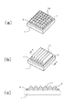
この最外層の凸部は、この層の断面において、円弧、楕円弧もしくは山形からなる群より選ばれた少なくとも1つの形状を有するものであることが好ましい。ここで、層の断面において円弧もしくは楕円弧とは、図2(a)に示すように最外層に半球状の突起物が並んだもののほか、図2(b)のような半円柱状のものも含まれる。また、この層の断面において山形とは、図1(a)に示すような錐状体のほか、図1(b)に示すような柱状も含まれる。
【0023】
最外層の凸部の形状を変えることにより、多層被覆基板に様々な機能を付与することができる。例えば、多層被覆基板を光学部品として使用する場合は、図2(a)もしくは(b)に記載の凸部を設けることにより、これに平板マイクロレンズアレイとしての機能を付与することができる。同様に、図1(a)もしくは(b)に記載の形状の凸部を設けることにより、多層被覆基板にグレーティングレンズとしての機能を付与することができる。このように、上記最外層の凸部の形状は、その目的に応じて変更することができる。そして、この発明の多層被覆基板は、それらの目的を高い次元で達成することができる。
【0024】
上述のように多層被覆基板の製造にはゾルゲル法を用いるが、ゾルゲル法の特徴として、厚い層を成形し難いという点が挙げられる。これは、層が厚くなるにしたがって、層の表面と内部との縮重合反応の進行度の差が大きくなり易いことに起因する。すなわち、ゾルゲル法では、金属アルコキシドが縮重合するにより、層が、溶液→ゾル→ゲル→固体へと変化する。この縮重合反応が進行するにしたがって、水が発生する。そして、この水が飽和した状態においては、縮重合反応が進行し難くなる。層の表面は、縮重合反応で発生した水を外部に放出できるので、水が飽和し難く、縮重合反応が進行し易い。これに対し、層の内部は、縮重合反応により発生した水が滞留するので、飽和状態になり易い。すなわち、層の内部は、縮重合反応が進行し難く、固化し難い。
【0025】
したがって、層の内部の縮重合反応が進行していなくても、層の表面はゲル化もしくは固化してしまうので、層の表面に引張り応力が発生する。これにより、層の表面にクラックが発生し易くなる。この引張り応力は、層の厚さが厚くなるにしたがって、大きくなる傾向にある。このため、ゾルゲル法では、層の厚いものが製造できない。実際にゾルゲル法で、3μm厚のテトラアルコキシシランの層を、ゾルから直接固化させた場合、その表面にクラックが発生する。また、20μm厚のメチルトリアルコキシシランの層を、ゾルから直接固化させた場合、その表面にクラックが発生する。
【0026】
最外層の凸部を大きくすることができれば、多層被覆基板に新たな特徴を付加することができる。例えば、多層被覆基板をレンズアレイとして利用する場合、焦点距離を短くすることができる。また、グレーティング素子として利用する場合、周期構造が粗なエシェル格子やエシェレット格子を製造できる。情報記録媒体として利用する場合には、多層記録といった機能を付与できる。
【0027】
最外層の凸部を大きくし、多層被覆基板に上記機能を与えるために、最外層の形状に合わせて、下層にも凸部を設けることが好ましい。これは、具体的には、図1(c)もしくは図2(c)に示す態様をいう。このように下層に凸部を設けることにより、各層の厚さを厚くすることなく、凸部の大きい多層被覆基板を得ることができる。すなわち、各層表面のクラックの発生を防ぐと同時に、最外層に大きな凸部を具える多層被覆基板を製造することができる。
【0028】
この多層被覆基板の各層は、ゲル状の仮成形時に、凸部を形成されることが好ましい。これは、各層の成形型に凹部を設けることで達成される。
【0029】
仮成形された各層は、ゲル状で積層され、その後最外層の型で加圧され、加熱されて固化する。積層基板全体として厚くても、積層により各層自体を薄くすることができる。したがって、各層は、その表面と内部とで縮重合反応の進行度に差ができ難く、応力が発生し難い。すなわち、各層をゲル状で積層することにより、各層の表面には、クラックが発生し難くなる。
【0030】
上記複数の層において、最も厚い層と最も薄い層との厚さ比すなわち(最も厚い層の厚さ)/(最も薄い層の厚さ)は、1〜5であることが好ましい。ここで、層の厚さとは、溶液もしくはゾルが型に注がれた段階における最も厚い部分、すなわち図4(c)に示すDの部分である。厚さ比がこの範囲内にある場合は、ゲル化および固化における縮重合反応の進行度にばらつきができ難い。したがって、各層の厚さが近い範囲にあるので、多層被覆基板全体において均一な層を製造することができる。これにより、各層にクラックが発生し難くなる。この比のさらに好ましい値は、1〜1.2であり、最も好ましい値は1であって、すべての層が同じ厚さであることが最適である。
【0031】
この複数の層において、各層の厚さは、特に限定されるものではないが、0.1〜20μmであることが好ましい。各層の厚さが20μmよりも厚くなると、クラックの発生が著しくなる。反対に、0.1μmより薄くなると、最外層および下層の凸部を成形し難くなり、製造上問題がある。
【0032】
上記最外層の凸部の高さは、特に限定されるものではないが、0.1〜40μmであることが好ましい。ここで、凸部の高さとは、図3におけるLをいう。これは、この値が0.1μmより小さくなると、凸部の機能が発揮し難くなる。すなわち、光学レンズに使用する場合は、0.1μm以下になると光の集束もしくは拡散性能が低くなり、レンズとしての機能を発揮し難くなる。反対に、この値が、40μmより大きくなると、製造過程において表面にクラックが発生し易くなる。
【0033】
複数の層は、その成分が各層同じあってもよいし、それぞれに異なっていてもよい。各層の成分が同じ場合は、均一で厚い被覆層を具えた多層被覆基板を得ることができる。対して、各層の成分を変更すると、多層被覆基板に様々な性質を付加することができる。
【0034】
例えば、オルガノポリシロキサンに、チタン、ジルコニウム、アルミニウム、鉛、タンタルなどの金属の酸化物を加えることにより、その層の屈折率を高くすることができる。また反対に、屈折率を低くするには、オルガノポリシロキサンに、ボロン、フッ素などを加えることで実現できる。このように各層の屈折率を変えることにより、多層被覆基板を光学部品として使用する場合、光の集束もしくは拡散特性を自由に調節できるようになる。
【0035】
また、オルガノポリシロキサンにおける有機性官能基の比率を調節することにより、各層に新たな機能を持たせることができる。ここで、有機性官能基とは、メチル、エチル、n−プロピル、イソプロピル、n−(βアミノエチル)−γ−アミノプロピル、フェニルまたはクロロフェニル基などである。例えば、この有機性官能基の重量率が高いオルガノポリシロキサンからなる層は、この重量率の低い層よりも脆性が抑制され、その表面にクラックが発生し難い。ただし、有機性官能基の重量率が高くなりすぎると、多層被覆基板の耐熱性が悪くなる。したがって、オルガノポリシロキサンにおける有機性官能基の重量率は、20〜60重量%が好ましい。
【0036】
多層被覆基板において、上述のように各層の成分を変更すると、各層の線膨張率が変化する。この線膨張率は、基板から最外層に向かって段階的に変化することが好ましい。すなわち、各層の線膨張率が段階的に変化することにより、この基板が熱に曝されても、各層が剥離しに難くなる。つまり、多層被覆基板の耐熱性が高くなる。
【0037】
また、隣接層間の線膨張率の差は、±5×10⁻⁶mm/℃であることが好ましい。この範囲にあるときに、多層被覆基板は、300℃に加熱されても層間剥離を起こさない。すなわち、このような多層被覆基板は、はんだ付けにも耐えられる。
【0038】
また、複数の層は、2層であることが好ましい。層の数が少ないほど、製造工数が少なくなるからである。
【0039】
基板の種類は、特に限定されるのもではないが、ガラスなどの透明体であることが好ましい。透明体を基板に持つ多層被覆基板は、レンズもしくは透過型回折格子としての機能を発揮することができる。対して、基板が不透明な場合は、反射型回折格子、反射型フレネルリフレクタ、もしくはCD−ROMなどの情報記録媒体としての利用が適当である。例えば、アルミニウム基板などがこれに当たる。
【0040】
さらに、多層被覆基板をレンズあるいは回折格子とする場合は、上述のように各層の成分を変更し、その屈折率を最下層から最外層に向けて段階的に変えることが好ましい。例えば、最下層から最外層に向けて屈折率が段階的に高くなると、光の集束がよくなり、レンズの集光性能が高くなる。また、内部反射による迷光が減り、光の分解能が高くなるので、回折格子としての性能が高くなる。
【0041】
また、この多層被覆基板を光学素子として使用する場合は、tx/nx=λ/4の関係が充たされていることが好ましい。ここで、txは任意の層の厚さであり、nxはその層の屈折率であり、λはその層を透過する光の波長である。この条件が充たされている多層被覆基板は、光の内部反射量が極めて少なくなる。したがって、この条件を充たす各層を有する多層被覆基板は、レンズあるいは回折格子としての高い機能を発揮することができる。使用する光の波長が決まっているのであれば、この式にしたがうことにより、各層の厚さと屈折率との最適値を求めることができる。
【0042】
さらには、最下層の屈折率をna、中間層の屈折率をnb、最外層の屈折率をno、基板の屈折率をnsとする場合、多層被覆基板は、na/nb=√(ns/no)の関係を充たすことが好ましい。なお、この関係式において、na≧nbであれば、さらに好適である。この関係を充たす多層被覆基板は、通常光学素子表面に成膜される無反射コーティングでは防止できない反射光も取り除くことができる。
【0043】
多層被覆基板を光学素子として使用する場合、使用する光は、その波長が380〜2,000nmであることが好ましい。この範囲の波長には、可視光と赤外光とが含まれるので、この多層被覆基板の汎用性が極めて高くなる。したがって、可視光であれば、液晶プロジェクタの液晶窓への集光レンズ、赤外光であれば、通信用のレーザもしくはLEDと光ファイバとの結合レンズとして、この多層被覆基板を使用することができる。
【0044】
多層被覆基板の各層は、オルガノポリシロキサンを含むものであればその材料を特に限定されないが、最外層がメチルトリエトキシシランからなり、下層がメチルトリエトキシシランもしくはテトラエトキシシランからなることが好ましい。メチルトリエトキシシランは、有機性官能基の重量率が比較的高く、層の仮成形および固化においてその表面にクラックが発生し難い。すなわち、メチルトリエトキシシランを最外層に用いることにより、多層被覆基板の不良品発生率を低く抑えることができる。また、メチルトリエトキシシランからなる層は、その骨格であるSi−O結合すなわち共有結合の比率が高いので、耐熱性がよい。したがって、メチルトリエトキシシランを最外層と下層とに用いることにより、クラックが発生し難くかつ耐熱性のよい多層被覆基板を製造することができる。
【0045】
また、最外層にメチルトリエトキシシラン、下層にテトラエトキシシランを用いることにより、多層被覆基板全体の一体性を高めることができる。これは、基板にガラス板を用いる場合、テトラエトキシシランの性質が、ガラス板とメチルトリエトキシシランの中間であることによる。ここで、中間の性質とは、具体的には屈折率と線膨張率とを指す。すなわち、下層(テトラエトキシシラン)の屈折率と線膨張率とが、基板(ガラス板)と最外層(メチルトリエトキシシラン)との中間であることにより、基板、下層および最外層の接着性が向上し、多層被覆基板全体としての一体性が高まる。
【0046】
上述のように、この発明は、オルガノポリシロキサンを含む溶液を基板上もしくは型内に流し込み、各層を個別にゲル状まで仮成形し、このゲルを積層し基板と一体化させることを特徴とする。ここで、仮成形後積層時のゲルの粘度は、1×10⁴〜1×10⁶Pの範囲であることが好ましい。粘度がこの範囲の場合は、積層作業ではゲルは変形しないが、その後の最外層の型の押圧によっては、ゲルの変形が可能である。
【0047】
この発明の製造方法は、各層をゲル状で積層し、その後最外層の型でこれらの層を押圧し密着させるので、基板と層あるいは層と層との間に隙間ができ難い。これも、この発明の製造方法の利点である。
【0048】
上述のようにゾルゲル法においては、表面のクラックの発生を防止するために、各層は薄い方が好ましい。しかしながら、多層被覆基板は、大きな凸部を具える必要がある。これは、多層被覆基板が大きな凸部を具えることにより、新たな性能を具えることができるからである。例えば、多層被覆基板がレンズアレイに使用される場合、凸部が大きいことにより焦点距離を短くすることができる。
【0049】
したがって、層の厚さは薄くかつ凸部は大きくという相反する要件を充たすために、最外層の凸部の形状に合わせて、下層にも凸部を設けることが好ましい。下層に凸部を設ける具体的方法として、図4および図5に記載の方法が挙げられる。この方法は、オルガノポリシロキサンの溶液を、窪みができるように、型内に少な目に注ぐことが特徴である。この窪みと凸部を具えた各層を積層することにより、各層の厚さは薄くかつ凸部は大きくという要件を充たすことができる。
【0050】
溶液もしくはゾル状をゲルに仮成形する硬化温度は、20〜120℃であることが好ましい。これは、20℃以下では加水分解、縮重合反応が進行し難くなり、120℃以上では、反応が早すぎてゲル状で反応を一度停止することが困難だからである。この仮成形時において、反応が進行しすぎた場合、層同士の接着強度が落ち、多層被覆基板の耐熱性が悪くなる。
【0051】
そして、その後これらのゲルを積層し、積層ゲルを基板と一体化(固化)させる。その時の温度は、50〜150℃であることが好ましい。これは、50℃以下では固化に要する時間が非常に長くなり、150℃以上では、反応が急速に進行するため、各層の表面にクラックが発生し易くなるからである。
【0052】
【実施例】
以下、実施例および比較例により、この発明をさらに具体的に説明する。なお、この発明は、以下の実施例に限定されるものではない。多層被覆基板の製造方法は、概略以下の手順で行われる。(1)オルガノポリシロキサン溶液を製造する→(2)この溶液を型に塗布する→(3)各層を仮成形(ゲル化)させる→(4)このゲルを基板上に積層する→(5)積層ゲルと基板とを一体化させる。そして、上記手順により製造された多層被覆基板を、各種の性能試験で評価した。
【0053】
(多層被覆基板の製造方法)
(1)オルガノポリシロキサン溶液を製造するテトラエトキシシラン64gをエタノール14gに混合した。この溶液を濃度0.2重量%の希塩酸(水溶媒)22gと混合し、濃度64重量%、100gのテトラエトキシシラン溶液を製造した。これを溶液1とする。
【0054】
つぎに、メチルトリエトキシシラン60gをエタノール16gに混合した。この溶液を濃度0.2重量%の希塩酸(水溶媒)24gと混合し、濃度60重量%、100gのメチルトリエトキシシラン溶液を製造した。これを溶液2とする。
【0055】
また、100gの溶液1にチタンノーマルブトキシド26gを混合し、20TiO2・80SiO2を得た。これを溶液3とする。
【0056】
(2)溶液を型に塗布する上記の溶液を、基板上および型に塗布した。まず、溶液1〜3のいずれかを図4(a)に示すように、ガラス板1の上にスピンコーティング法により塗布した。ここで、スピンコーティング法の代わりに、ディップコーティング法を用いてもよい。この溶液が塗布されたガラス板を室温(26℃)で30分間放置し自然乾燥させ、溶液がガラス板上で所望の厚さになるように調節した。この所望の厚さは、各層の溶液の種類により異なる。なお、各層の厚さtxは、He−Neレーザの波長λ=0.63μmと固化した層の屈折率nxとにより、tx=λ/4×nxで算出される。このガラス板に接した層が、多層被覆基板の最下層となる。
【0057】
同様に、前記溶液1〜3のいずれかを最外層の型に、スピンコーティング法により塗布した。上記同様、スピンコーティング法の代わりに、ディップコーティング法を用いてもよい。この塗布溶液を室温(26℃)で30分間自然乾燥させた。最外層の型は、曲率半径50μm、深さ25μmの略球面弧の凹部を複数有するNi型(以下、球面型と称する)と、ピッチ4μm、深さ2μm、頂角45゜のV溝を複数有するNi型(以下、V溝型と称する)との2種類を用いた。なお、上記球面型を図4(c)に示す。
【0058】
最外層の型に塗布された溶液は、その凹部に入り込み、多層被覆基板の最外層の凸部を形作る。
【0059】
また、中間層は、最外層の凸部の形状に合わせて、最外層の凸部より小さい凸部を具えるように形成された。すなわち、中間層の型は、中間層の凸部が最外層の凸部と同じ位置に形成されるように、凹部を具える。本実施例では、3層に積層された多層被覆基板を製造するので、中間層は1層である。したがって、最外層の型が球面型の場合は、中間層の型に、曲率半径25μm、深さ12.5μmの凹部を具えたもの(以下、中間球面型と称する)を使用した。この中間球面型を図4(b)に示す。中間層の数が多くなる場合は、基板から最外層に向かって段階的に凹部が大きく深くなる中間層の型を使用することで、本発明の効果を発揮できる。
【0060】
ただし、最外層の型がV溝型の場合は、V溝が浅いので、中間層は、凸部を具えていなくても構わない。また、凸部を具えていない中間層の方が、離型し易いという利点がある。したがって、本実施例では、最外層の型にV溝型を使用する場合は、ポリカーボネートの平板を中間層の型として用いた。
【0061】
中間層を成形するために、溶液1〜3のいずれかを中間球面型もしくはポリカーボネート板に、スピンコーティング法により塗布した。この溶液を室温(26℃)で30分間自然乾燥させ、所望の厚さとなるように調節した。
【0062】
(3)各層を仮成形させる溶液を塗布したガラス板や型を、真空チャンバー中に配置し、減圧下で所定の温度に昇温して、仮成形した。仮成形時の背圧は、1×10⁻⁴mmHgで、時間は30分であった。また、仮成形時温度は、クラックの発生を防止するため、溶液1または溶液3の場合は50℃、溶液2の場合は80℃とした。これらの仮成形条件は、各層毎に最適な条件を選択した。そして、ゲルの粘度は1×10⁴Pとした。
【0063】
(4)ゲルを基板上に積層する中間層のゲルを離型し、これをガラス板上の最下層のゲル上に積層した。さらに、型に入ったままの最外層のゲルと前記積層ゲルとを接触させた。
【0064】
(5)積層ゲルと基板とを一体化させる前記最外層のゲルと積層ゲルとを、最外層の型で押圧しながら、減圧加熱して本成形した。本成形時の背圧は、1×10⁻⁴mmHgで、時間は120分であった。また、最外層の押圧力は2〜2.5kgf/cm2で、温度は、溶液1または溶液3の場合80℃、溶液2の場合120℃とした。
【0065】
(多層被覆基板の性能評価)
(凸部の高さのばらつき測定)多層被覆基板の最外層表面の任意の10mm角をサンプリングし、レーザ顕微鏡を用いて凸部の高さを測定した。
【0066】
(耐熱性試験)多層被覆基板を300℃で2時間保持し、その後室温に戻して、クラックあるいは層間剥離の発生を目視により観察した。
【0067】
(光学特性測定)上記耐熱性試験の前後で、He−Neレーザを用いて、回折格子の回折パターン、マイクロレンズの集光性能を測定し、その変化をみた。また、He−Neレーザを用いて、入射角約6゜で基板表面へレーザを照射した。そして、その反射総量から基板表面でのフレネル反射計算値を算出し、その値を差し引くことにより、基板内部での反射量を算出し、その変化を評価した。さらに、アッベ屈折率計を用いて、型平坦部におけるd線の屈折率を測定し、その変化を評価した。
【0068】
(実施例1)ソーダライムガラス板(基板)、ポリカーボネート板(中間層の型)およびV溝型(最外層の型)それぞれに、固化したときの厚さが2μmになるように溶液1を塗布し、仮成形を行った。ここで、V溝型における2μmは、仮成形後のゲルの最も厚い部分であり、図4(c)におけるDである。また、本成形時におけるV溝型の押圧力は、2kgf/cm2であった。
【0069】
以上の条件で製造された多層被覆基板は、透明であり、複数の層の厚さ6μm、屈折率1.39であった。この多層被覆基板は、回折格子として利用可能である。また、この多層被覆基板の凸部の高さのばらつきは、0.7μmであった。耐熱性試験の結果、この多層被覆基板にクラックまたは層間剥離は発生しなかった。さらに、光学特性測定の結果、回折パターン、内部反射量および屈折率に変化は見られなかった。
【0070】
なお、この多層被覆基板は、各層の成分が同じため、ゲルで積層された面が分からなかった。すなわち、複数の層は全く一体化していた。
【0071】
(実施例2)ソーダライムガラス板、中間球面型および球面型それぞれに、固化したときの厚さが17μmになるように溶液2を塗布し、仮成形を行った。ここで、前記17μmは、仮成形後のゲルの最も厚い部分の厚さである。また、本成形における球面型の押圧力は、2.5kgf/cm2であった。実施例2の多層被覆基板の製造工程を図4および図5に示す。
【0072】
以上の条件で製造された多層被覆基板は、透明であり、複数の層の厚さ50μm、屈折率1.45であった。ここで、複数の層の厚さとは、図5(e)におけるHである。この多層被覆基板はマイクロレンズとして機能し、その焦点距離が105μmであった。また、この多層被覆基板の凸部の高さのばらつきは、0.4μmであった。耐熱性試験の結果、多層被覆基板にクラックまたは層間剥離は発生しなかった。光学特性測定の結果、集光性能、内部反射量および屈折率に変化は見られなかった。
【0073】
なお、この多層被覆基板は、各層の成分が同じため、ゲルで積層された面が分からなかった。すなわち、複数の層は全く一体化していた。
【0074】
(実施例3)屈折率が1.70の光学ガラス板に、固化したときの厚さが0.24μmになるように溶液3を塗布した。また、ポリカーボネート板に、固化したときの厚さが2μmになるように溶液1を塗布し、これらを個別に仮成形した。実施例3では、実施例1および実施例2と異なり、最外層の型すなわち球面型もしくはV溝型を使用しなかった。したがって、製造される多層被覆基板は、光学ガラス板上の積層が2層であった。また、本成形時において、ポリカーボネート板を光学ガラス板に圧力2kgf/cm2で押圧して、多層被覆基板を製造した。
【0075】
以上の条件で製造された多層被覆基板は、複数の層の厚さ2μmであった。耐熱性試験の結果、多層被覆基板にクラックまたは層間剥離は発生しなかった。また、光学特性測定の内、内部反射量の測定のみ行った。その結果、内部反射量は、0.1%以下で、加熱前後でその値に変化は見られなかった。
【0076】
実施例1〜3の条件と結果とを、以下の表1にまとめる。
【表1】

以上の実施例により、以下のことが判る。本発明に関するオルガノポリシロキサンを含む複数の層を有するゾルゲル法による最外層に複数の凸部を有する多層被覆基板の製造方法によれば、耐熱性が高く、変色および層間剥離などの性能変化が発生しない多層被覆基板を得ることができる。
【0078】
【発明の効果】
本発明のゾルゲル法による最外層に複数の凸部を有する多層被覆基板の製造方法によれば、オルガノポリシロキサンの溶液を基板上および型内に流し込み、これらを個別にゲル化させ、その後これらのゲルを基板上に積層し、最外層の型で押圧しながら基板と一体化させるので、各層表面にクラックを発生させることなく、最外層の凸部の寸法精度の高い多層被覆基板を製造することができる。
【0079】
また本発明のゾルゲル法による最外層に複数の凸部を有する多層被覆基板の製造方法によれば、前記の発明の効果に加え、任意の層の断面形状を、円弧、楕円孤および山形からなる群より選ばれた少なくとも1つの形状に整形する型を使用するので、最外層の凸部が大きい多層被覆基板を製造することができる。
【0080】
また本発明のゾルゲル法による最外層に複数の凸部を有する多層被覆基板の製造方法によれば、前記の発明の効果に加え、オルガノポリシロキサンの溶液をゲル化させる温度が20〜120℃であって、その後の基板とゲルの積層体と一体化させる温度が50〜150℃であるので、各層にクラックを発生させることなく、能率良く多層被覆基板を製造することができる。
【0081】
また本発明のゾルゲル法による最外層に複数の凸部を有する多層被覆基板の製造方法によれば、前記の発明の効果に加え、1×10⁴〜1×10⁶Pのゲルを積層するので、積層する際にゲルの変形がなく、かつ基板と複数の層とが密着した多層被覆基板を容易に製造することができる。
【0082】
また本発明のゾルゲル法による最外層に複数の凸部を有する多層被覆基板の製造方法によれば、前記の発明の効果に加え、最外層をメチルトリエトキシシランから得られるゲル層とし、下層をメチルトリエトキシシランから得られるゲル層とすることにより、クラックが発生し難くかつ耐熱性のよい多層被覆基板を製造することができる。
【0083】
また本発明のゾルゲル法による最外層に複数の凸部を有する多層被覆基板の製造方法によれば、前記の発明の効果に加え、最外層をメチルトリエトキシシランから得られるゲル層とし、最下層をテトラエトキシシランから得られるゲル層とすることにより、多層被覆基板全体の一体性を高めることができる。
【図面の簡単な説明】
【図1】(a)は、最外層の凸部が錐状の山形である多層被覆基板の斜視図である
(b)は、最外層の凸部が柱状の山形である多層被覆基板の斜視図である
(c)は、A−A鎖線にしたがう断面図である
【図2】(a)は、最外層の凸部が半球状である多層被覆基板の斜視図である
(b)は、最外層の凸部が半円柱状である多層被覆基板の斜視図である
(c)は、B−B鎖線にしたがう断面図である
【図3】最外層の凸部が半円柱状である多層被覆基板の要部断面図である
【図4】(a)は、ガラス板にオルガノポリシロキサンの溶液を塗布した状態の概要図である
(b)は、中間球面型にオルガノポリシロキサンの溶液を塗布した状態の概要図である
(c)は、球面型にオルガノポリシロキサンの溶液を塗布した状態の概要図である
【図5】(d)は、仮成形されたゲルを積層し、本成形させる際の概要図である
(e)は、本成形後、複数の層が一体化した多層被覆基板の断面図である
【符号の説明】
1 ガラス板
2 最下層
3 中間層
4 最下層
5 中間層
10 凸部が錐状の山形である最外層
11 凸部が柱状の山形である最外層
12 凸部が半球状である最外層
13 凸部が半円柱状である最外層
30 中間球面型(中間層の型)
31 球面型(最外層の型)
40 一体化した複数の層
D 型に注がれた溶液の最も厚い部分
L 凸部の高さ
H 一体化した複数の層の厚さ[0001]
BACKGROUND OF THE INVENTION
The present invention relates to a method of manufacturing a multilayer coated substrate used as an information recording medium using magnetism or light or an optical component such as optical communication. More particularly, the present invention relates to a method for manufacturing a multilayer coated substrate used as an information recording medium such as a CD-ROM or an optical component such as a flat microlens or a grating element by a sol-gel method.
[0002]
[Prior art]
An optical component such as an information recording medium such as a CD-ROM, a flat microlens, or a grating element needs to have a minute convex portion on the surface thereof. The minute convex portion on the surface functions as a pit or tracking guide in the information recording medium, and functions as a microlens or a diffraction grating by focusing or diffusing light in the optical component.
[0003]
In order to form these convex portions on the surface, there is a method (Japanese Patent Laid-Open No. 63-49702) in which an ultraviolet curable resin is uniformly spread on a substrate, and the resin is irradiated with ultraviolet rays while being pressed with a mold having concave portions. Are known.
[0004]
Further, in Japanese Patent Application Laid-Open Nos. 62-102445 and 6-242303, a solution containing silicon alkoxide is applied on a glass substrate and heated while pressing a mold having a recess to form a protrusion. A so-called sol-gel manufacturing method is described.
[0005]
In addition, Japanese Patent Laid-Open No. 63-197382 discloses a method in which an ultraviolet curable resin is uniformly spread on a substrate and a convex portion is formed by reactive ion beam etching using a pattern formed of a photoresist as a mask. Are listed.
[0006]
[Problems to be solved by the invention]
However, the conventional technique has the following problems. First, the ultraviolet curable resin has low heat resistance, and decomposition and yellowing occur at 250 ° C. or higher. Therefore, the substrate having the convex portion of the ultraviolet curable resin cannot be subjected to heat processing such as soldering, and is difficult to be attached to an apparatus or the like.
[0007]
On the other hand, the convex part of the silicon alkoxide formed by the sol-gel method has high heat resistance and can be soldered. However, the sol-gel method has a problem that a thick film cannot be formed. When a silicon alkoxide layer of several tens of μm is actually formed by the sol-gel method, minute cracks (hereinafter referred to as cracks) are generated on the surface. This is because when the silicon alkoxide solution is gelled and solidified, the degree of progress of the polycondensation reaction can be different between the surface and the inside of the layer, so that a large stress is generated on the surface. Further, this layer may be peeled off from the substrate due to this stress.
[0008]
In addition, when forming convex portions using reactive ion beam etching, the manufacturing process is complicated and the manufacturing cost is high, and it is difficult to improve the uniformity of the convex portions. . Furthermore, for such reasons, it is difficult to form a layer having a large surface area.
[0009]
The present invention has been made paying attention to such problems existing in the prior art. The purpose is a multilayer coated substrate having high heat resistance, no cracks on the surface even if it is a thick layer and peeling from the substrate, and a layer having a uniform convex portion even in a large area Is to provide a method for easily and inexpensively producing the above.
[0010]
[Means for Solving the Problems]
In order to achieve the above object, a method for producing a multilayer coated substrate having a plurality of convex portions on the outermost layer by the sol-gel method of the present invention comprises a solution of an organopolysiloxane.GlassPour onto the substrate and in the mold, gel these individually,The viscosity of the gel is 1 × 10 Four ~ 1x10 6 In the state of POn the board2 layers or moreLaminated,It is integrated with the substrate while pressing with the outermost mold.
[0011]
The method for producing a multilayer coated substrate having a plurality of convex portions on the outermost layer by the sol-gel method of the present invention is the method for producing a multilayer coated substrate, wherein the cross-sectional shape of an arbitrary layer is a group consisting of an arc, an elliptic arc, and a mountain shape. A mold that is shaped into at least one selected shape is used.
[0012]
In the method for producing a multilayer coated substrate having a plurality of convex portions on the outermost layer by the sol-gel method of the present invention, the temperature for gelling the organopolysiloxane solution in the method for producing a multilayer coated substrate is 20 to 120 ° C. Then, the temperature at which the subsequent substrate and the gel laminate are integrated is 50 to 150 ° C.
[0013]
The method for producing a multilayer coated substrate having a plurality of convex portions on the outermost layer by the sol-gel method of the present invention is the method for producing a multilayer coated substrate, wherein the outermost layer is made of methyltriethoxysilane and the lower layer is made of methyltriethoxysilane. The gel consisting of is laminated.
[0014]
The method for producing a multilayer coated substrate having a plurality of convex portions on the outermost layer by the sol-gel method of the present invention is the method for producing a multilayer coated substrate, wherein the outermost layer is made of methyltriethoxysilane and is in contact with the substrate. Is a laminate of gels made of tetraethoxysilane.
[0015]
DETAILED DESCRIPTION OF THE INVENTION
Hereinafter, embodiments of the present invention will be described in detail. In the present invention, a plurality of layers are laminated on a substrate by a sol-gel method, the substrate and the plurality of layers are integrated, and a plurality of convex portions are provided on the outermost layer. The plurality of convex portions have small variations in height and extremely high uniformity. The high uniformity of the convex portion is the same not only for the height but also for the overall outer shape. That is, the width and depth of the convex portions are highly uniform. Furthermore, the uniformity is high with respect to the internal stress or component concentration generated in the convex portions and the plurality of layers. Therefore, a substrate integrated with a plurality of layers, that is, a multilayer coated substrate, exhibits extremely high performance in each application. That is, the multilayer coated substrate can be a highly accurate flat microlens array having a large number of microlenses with uniform performance. Alternatively, it can be a diffraction grating with extremely high resolution capability.
[0016]
In the plurality of layers, the outermost layer refers to the uppermost surface layer with reference to the substrate, and the lower layer refers to a layer other than the outermost layer. Furthermore, this lower layer consists of a lowermost layer in contact with the substrate and other intermediate layers.
[0017]
The manufacturing method of the multilayer coated substrate of the present invention is based on the sol-gel method. First, each layer is temporarily formed into a gel by a solution containing an organopolysiloxane being individually poured into each mold and heated or decompressed. At this time, the solution forming the lowermost layer may be poured directly onto the substrate. Next, each gel-like layer is removed from the mold and laminated on the substrate. The laminated gel is heated while being pressed against the substrate by the outermost mold, and is integrated with the substrate.
[0018]
The polycondensation reaction of the organopolysiloxane is completed by heating the laminated gel on the substrate. That is, the gel is completely solidified and a multilayer coated substrate is formed. During this heating, the surface shape of this mold can be transferred to the outermost layer by pressing the laminated gel against the substrate with the outermost mold. Therefore, the surface shape of this mold is copied to the outermost layer as it is. Moreover, the shape of the convex part of the outermost layer can be variously adjusted by changing the surface shape of this mold.
[0019]
A feature of the present invention is that each layer is individually temporarily formed into a gel using a sol-gel method, and then each layer is laminated to produce a multilayer coated substrate. A method for producing a multilayer coated substrate using a sol-gel method has been known (Japanese Patent Laid-Open No. 6-242303). However, in the conventional manufacturing method, the constituent components of each layer are spread on a substrate with a solution or sol, and are heated with pressure while being pressed with a mold to form the layers all at once. Then, a solution or sol was further poured onto the completely solidified layer to form an upper layer.
[0020]
In this way, the method of forming each layer sequentially has a long manufacturing process, which causes an increase in cost and is not suitable for actual production. Further, in this method, since the next layer is injected after the lower layer is completely cured, unnecessary air easily enters between the mold and the solution or sol, and the dimensional accuracy of the multilayer coated substrate is not high.
[0021]
On the other hand, in the present invention, since each layer is laminated in a gel form, the manufacturing process of the multilayer coated substrate is short and its dimensional accuracy is extremely high. Specifically, the variation in the height of the convex portion of the outermost layer according to the present invention is 1 μm or less. Here, the height of the convex portion of the outermost layer is the distance L shown in FIG.
[0022]
The convex portion of the outermost layer preferably has at least one shape selected from the group consisting of an arc, an elliptical arc, or a mountain shape in the cross section of the layer. Here, in the cross section of the layer, an arc or an elliptical arc is one in which hemispherical projections are arranged in the outermost layer as shown in FIG. included. In addition, in the cross section of this layer, the chevron includes not only a conical body as shown in FIG. 1 (a) but also a pillar shape as shown in FIG. 1 (b).
[0023]
By changing the shape of the convex portion of the outermost layer, various functions can be imparted to the multilayer coated substrate. For example, when a multilayer coated substrate is used as an optical component, by providing the convex portion shown in FIG. 2A or 2B, a function as a flat microlens array can be imparted thereto. Similarly, by providing a convex portion having the shape shown in FIG. 1A or 1B, a function as a grating lens can be imparted to the multilayer coated substrate. Thus, the shape of the convex part of the outermost layer can be changed according to the purpose. And the multilayer coated substrate of this invention can achieve those objectives in a high dimension.
[0024]
As described above, the sol-gel method is used for the production of the multi-layer coated substrate. As a feature of the sol-gel method, it is difficult to form a thick layer. This is because the difference in the degree of progress of the condensation polymerization reaction between the surface of the layer and the inside tends to increase as the layer becomes thicker. That is, in the sol-gel method, the metal alkoxide undergoes polycondensation, whereby the layer changes from solution → sol → gel → solid. As this polycondensation reaction proceeds, water is generated. And in the state which this water was saturated, it becomes difficult for a polycondensation reaction to advance. Since the surface of the layer can release the water generated by the condensation polymerization reaction to the outside, the water is hardly saturated and the condensation polymerization reaction easily proceeds. On the other hand, since the water generated by the polycondensation reaction stays inside the layer, it is easily saturated. That is, the condensation polymerization reaction does not easily proceed inside the layer and is not easily solidified.
[0025]
Therefore, even if the condensation polymerization reaction inside the layer does not proceed, the surface of the layer is gelled or solidified, and tensile stress is generated on the surface of the layer. Thereby, cracks are likely to occur on the surface of the layer. This tensile stress tends to increase as the layer thickness increases. For this reason, a thick layer cannot be manufactured by the sol-gel method. When a 3 μm thick tetraalkoxysilane layer is actually solidified directly from the sol by the sol-gel method, cracks are generated on the surface. Further, when a 20 μm thick methyltrialkoxysilane layer is solidified directly from the sol, cracks are generated on the surface thereof.
[0026]
If the convex portion of the outermost layer can be increased, a new feature can be added to the multilayer coated substrate. For example, when a multilayer coated substrate is used as a lens array, the focal length can be shortened. Further, when used as a grating element, an echelle grating or an echellet grating having a rough periodic structure can be manufactured. When used as an information recording medium, a function such as multilayer recording can be provided.
[0027]
In order to enlarge the convex part of the outermost layer and to give the above function to the multilayer coated substrate, it is preferable to provide the convex part on the lower layer in accordance with the shape of the outermost layer. Specifically, this refers to the embodiment shown in FIG. 1 (c) or FIG. 2 (c). Thus, by providing a convex part in the lower layer, a multilayer coated substrate having a large convex part can be obtained without increasing the thickness of each layer. That is, it is possible to manufacture a multilayer coated substrate having a large convex portion on the outermost layer while preventing the occurrence of cracks on the surface of each layer.
[0028]
Each layer of the multilayer coated substrate is preferably formed with a convex portion at the time of gel-like temporary molding. This is achieved by providing recesses in the molds for each layer.
[0029]
Each temporarily formed layer is laminated in a gel form, and then pressed with the outermost mold and heated to solidify. Even if it is thick as a whole laminated substrate, each layer itself can be made thin by lamination. Therefore, each layer is unlikely to have a difference in the degree of progress of the condensation polymerization reaction between the surface and the inside, and stress is hardly generated. That is, by laminating each layer in a gel state, cracks are unlikely to occur on the surface of each layer.
[0030]
In the plurality of layers, the thickness ratio between the thickest layer and the thinnest layer, that is, (thickest layer thickness) / (thinnest layer thickness) is preferably 1 to 5. Here, the thickness of the layer is the thickest portion at the stage where the solution or sol is poured into the mold, that is, the portion D shown in FIG. When the thickness ratio is within this range, it is difficult to vary the degree of progress of the condensation polymerization reaction in gelation and solidification. Therefore, since the thickness of each layer is in the close range, a uniform layer can be manufactured over the entire multilayer coated substrate. This makes it difficult for cracks to occur in each layer. A more preferred value for this ratio is 1 to 1.2, the most preferred value is 1, and it is optimal that all layers have the same thickness.
[0031]
In the plurality of layers, the thickness of each layer is not particularly limited, but is preferably 0.1 to 20 μm. When the thickness of each layer is greater than 20 μm, the occurrence of cracks becomes significant. On the other hand, when the thickness is less than 0.1 μm, it becomes difficult to form the outermost and lower layer convex portions, which causes a problem in manufacturing.
[0032]
The height of the convex portion of the outermost layer is not particularly limited, but is preferably 0.1 to 40 μm. Here, the height of the convex portion refers to L in FIG. If this value is smaller than 0.1 μm, the function of the convex portion becomes difficult to be exhibited. That is, when used for an optical lens, if the thickness is 0.1 μm or less, the light focusing or diffusing performance is lowered, and the function as a lens is hardly exhibited. On the other hand, if this value is larger than 40 μm, cracks are likely to occur on the surface during the manufacturing process.
[0033]
The plurality of layers may have the same or different components. When the components of the respective layers are the same, a multilayer coated substrate having a uniform and thick coating layer can be obtained. On the other hand, by changing the components of each layer, various properties can be added to the multilayer coated substrate.
[0034]
For example, the refractive index of the layer can be increased by adding an oxide of a metal such as titanium, zirconium, aluminum, lead, or tantalum to the organopolysiloxane. On the other hand, the refractive index can be lowered by adding boron, fluorine or the like to the organopolysiloxane. By changing the refractive index of each layer in this way, the light focusing or diffusing characteristics can be freely adjusted when the multilayer coated substrate is used as an optical component.
[0035]
Moreover, a new function can be given to each layer by adjusting the ratio of the organic functional group in organopolysiloxane. Here, the organic functional group is a methyl, ethyl, n-propyl, isopropyl, n- (β aminoethyl) -γ-aminopropyl, phenyl or chlorophenyl group. For example, a layer made of an organopolysiloxane having a high weight ratio of organic functional groups is less brittle than a layer having a low weight ratio, and cracks are less likely to occur on the surface thereof. However, if the weight ratio of the organic functional group is too high, the heat resistance of the multilayer coated substrate is deteriorated. Therefore, the weight ratio of the organic functional group in the organopolysiloxane is preferably 20 to 60% by weight.
[0036]
In the multilayer coated substrate, when the component of each layer is changed as described above, the linear expansion coefficient of each layer changes. This linear expansion coefficient preferably changes stepwise from the substrate toward the outermost layer. That is, since the linear expansion coefficient of each layer changes stepwise, even if this substrate is exposed to heat, each layer is difficult to peel off. That is, the heat resistance of the multilayer coated substrate is increased.
[0037]
The difference in linear expansion coefficient between adjacent layers is ± 5 × 10⁻⁶It is preferable that it is mm / ° C. When in this range, the multilayer coated substrate does not cause delamination even when heated to 300 ° C. That is, such a multilayer coated substrate can withstand soldering.
[0038]
The plurality of layers are preferably two layers. This is because the smaller the number of layers, the smaller the number of manufacturing steps.
[0039]
Although the kind of board | substrate is not specifically limited, It is preferable that they are transparent bodies, such as glass. A multilayer coated substrate having a transparent body as a substrate can exhibit a function as a lens or a transmission type diffraction grating. On the other hand, when the substrate is opaque, use as an information recording medium such as a reflective diffraction grating, a reflective Fresnel reflector, or a CD-ROM is appropriate. For example, an aluminum substrate corresponds to this.
[0040]
Further, when the multilayer coated substrate is a lens or a diffraction grating, it is preferable to change the components of each layer as described above and change the refractive index stepwise from the lowermost layer to the outermost layer. For example, when the refractive index increases stepwise from the lowermost layer toward the outermost layer, the focusing of light is improved and the light condensing performance of the lens is improved. Further, stray light due to internal reflection is reduced and the resolution of light is increased, so that the performance as a diffraction grating is enhanced.
[0041]
Further, when this multilayer coated substrate is used as an optical element, it is preferable that the relationship of tx / nx = λ / 4 is satisfied. Here, tx is the thickness of an arbitrary layer, nx is the refractive index of the layer, and λ is the wavelength of light transmitted through the layer. A multilayer coated substrate that satisfies this condition has a very small amount of internal reflection of light. Therefore, the multilayer coated substrate having each layer satisfying this condition can exhibit a high function as a lens or a diffraction grating. If the wavelength of light to be used is determined, the optimum value of the thickness and refractive index of each layer can be obtained by following this equation.
[0042]
Furthermore, when the refractive index of the lowermost layer is na, the refractive index of the intermediate layer is nb, the refractive index of the outermost layer is no, and the refractive index of the substrate is ns, the multilayer coated substrate can be expressed as na / nb = √ (ns / no)). In this relational expression, it is more preferable if na ≧ nb. A multilayer coated substrate that satisfies this relationship can also remove reflected light that cannot be prevented by a non-reflective coating that is normally deposited on the surface of the optical element.
[0043]
When the multilayer coated substrate is used as an optical element, the wavelength of the light used is preferably 380 to 2,000 nm. Since wavelengths in this range include visible light and infrared light, the versatility of this multilayer coated substrate becomes extremely high. Therefore, this multilayer coated substrate can be used as a condensing lens for a liquid crystal window of a liquid crystal projector if it is visible light, or as a coupling lens between a laser or LED and an optical fiber for communication if it is infrared light. it can.
[0044]
The material of each layer of the multilayer coated substrate is not particularly limited as long as it contains organopolysiloxane, but the outermost layer is preferably made of methyltriethoxysilane and the lower layer is preferably made of methyltriethoxysilane or tetraethoxysilane. Methyltriethoxysilane has a relatively high weight ratio of organic functional groups, and cracks are hardly generated on the surface of the layer during temporary molding and solidification. That is, by using methyltriethoxysilane as the outermost layer, the defective product occurrence rate of the multilayer coated substrate can be kept low. In addition, the layer made of methyltriethoxysilane has a high heat resistance since the ratio of Si—O bond, that is, covalent bond, which is the skeleton thereof is high. Therefore, by using methyltriethoxysilane for the outermost layer and the lower layer, it is possible to produce a multilayer coated substrate that hardly causes cracks and has good heat resistance.
[0045]
Further, by using methyltriethoxysilane for the outermost layer and tetraethoxysilane for the lower layer, the integrity of the entire multilayer coated substrate can be enhanced. This is because when a glass plate is used for the substrate, the nature of tetraethoxysilane is intermediate between that of the glass plate and methyltriethoxysilane. Here, the intermediate property specifically refers to a refractive index and a linear expansion coefficient. That is, since the refractive index and the linear expansion coefficient of the lower layer (tetraethoxysilane) are intermediate between the substrate (glass plate) and the outermost layer (methyltriethoxysilane), the adhesion of the substrate, the lower layer, and the outermost layer is improved. This improves the integrity of the multilayer coated substrate as a whole.
[0046]
As described above, the present invention is characterized in that a solution containing an organopolysiloxane is poured onto a substrate or in a mold, each layer is individually formed into a gel, and the gel is laminated and integrated with the substrate. . Here, the viscosity of the gel at the time of lamination after temporary molding is 1 × 10Four~ 1x10⁶The range of P is preferable. When the viscosity is in this range, the gel is not deformed in the laminating operation, but the gel can be deformed depending on the subsequent pressing of the outermost layer mold.
[0047]
In the manufacturing method of the present invention, the layers are laminated in a gel form, and then these layers are pressed and adhered with the outermost mold, so that it is difficult to form a gap between the substrate and the layer or between the layers. This is also an advantage of the manufacturing method of the present invention.
[0048]
As described above, in the sol-gel method, each layer is preferably thin in order to prevent generation of cracks on the surface. However, the multilayer coated substrate needs to have a large convex portion. This is because the multilayer coated substrate can have new performance by having a large convex portion. For example, when a multilayer coated substrate is used for a lens array, the focal length can be shortened due to the large convex portion.
[0049]
Therefore, in order to satisfy the conflicting requirements that the thickness of the layer is thin and the convex portion is large, it is preferable to provide the convex portion on the lower layer in accordance with the shape of the convex portion of the outermost layer. As a specific method of providing a convex portion in the lower layer, the methods described in FIGS. 4 and 5 can be given. This method is characterized in that a solution of the organopolysiloxane is poured into the mold with a small amount so as to form a recess. By laminating the layers having the depressions and the protrusions, it is possible to satisfy the requirement that the thickness of each layer is thin and the protrusions are large.
[0050]
The curing temperature at which the solution or sol is temporarily formed into a gel is preferably 20 to 120 ° C. This is because hydrolysis and polycondensation reactions hardly proceed at 20 ° C. or lower, and it is difficult to stop the reaction once in a gel state at 120 ° C. or higher. If the reaction proceeds excessively during the temporary molding, the adhesive strength between the layers decreases, and the heat resistance of the multilayer coated substrate deteriorates.
[0051]
Then, these gels are laminated, and the laminated gel is integrated (solidified) with the substrate. The temperature at that time is preferably 50 to 150 ° C. This is because the time required for solidification becomes very long at 50 ° C. or lower, and the reaction proceeds rapidly at 150 ° C. or higher, so that cracks are likely to occur on the surface of each layer.
[0052]
【Example】
Hereinafter, the present invention will be described more specifically with reference to examples and comparative examples. The present invention is not limited to the following examples. The method for producing a multilayer coated substrate is generally performed according to the following procedure. (1) Manufacture organopolysiloxane solution → (2) Apply this solution to the mold → (3) Temporarily mold (gelate) each layer → (4) Laminate this gel on the substrate → (5) The laminated gel and the substrate are integrated. And the multilayer coated substrate manufactured by the said procedure was evaluated by various performance tests.
[0053]
(Manufacturing method of multilayer coated substrate)
(1) 64 g of tetraethoxysilane for producing an organopolysiloxane solution was mixed with 14 g of ethanol. This solution was mixed with 22 g of dilute hydrochloric acid (aqueous solvent) having a concentration of 0.2% by weight to prepare a tetraethoxysilane solution having a concentration of 64% by weight and 100 g. This is
[0054]
Next, 60 g of methyltriethoxysilane was mixed with 16 g of ethanol. This solution was mixed with 24 g of diluted hydrochloric acid (aqueous solvent) having a concentration of 0.2% by weight to prepare a methyltriethoxysilane solution having a concentration of 60% by weight and 100 g. This is Solution 2.
[0055]
Further, 26 g of titanium normal butoxide was mixed with 100 g of
[0056]
(2) Applying the solution to the mold The above solution was applied to the substrate and the mold. First, as shown in FIG. 4A, any one of the
[0057]
Similarly, any one of the
[0058]
The solution applied to the mold of the outermost layer enters the concave portion and forms the convex portion of the outermost layer of the multilayer coated substrate.
[0059]
Further, the intermediate layer was formed so as to have a convex portion smaller than the convex portion of the outermost layer in accordance with the shape of the convex portion of the outermost layer. That is, the mold of the intermediate layer has a concave portion so that the convex portion of the intermediate layer is formed at the same position as the convex portion of the outermost layer. In this embodiment, since a multilayer coated substrate laminated in three layers is manufactured, the intermediate layer is one layer. Therefore, when the outermost layer mold was a spherical mold, an intermediate layer mold having a recess with a radius of curvature of 25 μm and a depth of 12.5 μm (hereinafter referred to as an intermediate spherical mold) was used. This intermediate spherical surface type is shown in FIG. When the number of intermediate layers increases, the effect of the present invention can be exhibited by using an intermediate layer mold in which the recesses become larger and deeper stepwise from the substrate toward the outermost layer.
[0060]
However, when the outermost layer type is a V-groove type, the V-groove is shallow, so the intermediate layer may not have a convex portion. Moreover, the intermediate layer which does not have a convex part has the advantage that it is easy to release. Therefore, in this example, when a V-groove type was used as the outermost layer mold, a polycarbonate flat plate was used as the intermediate layer mold.
[0061]
In order to form the intermediate layer, any one of the
[0062]
(3) A glass plate or a mold to which a solution for temporarily forming each layer was applied was placed in a vacuum chamber, and the temperature was raised to a predetermined temperature under reduced pressure to perform temporary molding. Back pressure during temporary molding is 1 × 10-FourThe time was 30 minutes at mmHg. The temperature at the time of temporary molding was set to 50 ° C. in the case of
[0063]
(4) The gel of the intermediate layer for laminating the gel on the substrate was released, and this was laminated on the lowermost gel on the glass plate. Furthermore, the outermost layer gel kept in the mold was brought into contact with the laminated gel.
[0064]
(5) The outermost layer gel and the laminated gel for integrating the laminated gel and the substrate were heated under reduced pressure while being pressed with the outermost layer mold to perform the main molding. Back pressure during main molding is 1 × 10-FourThe time was 120 minutes at mmHg. Moreover, the pressing force of the outermost layer is 2 to 2.5 kgf / cm.2The temperature was 80 ° C. for
[0065]
(Performance evaluation of multilayer coated substrate)
(Measurement of variation in height of convex portion) An arbitrary 10 mm square on the outermost layer surface of the multilayer coated substrate was sampled, and the height of the convex portion was measured using a laser microscope.
[0066]
(Heat resistance test) The multilayer coated substrate was held at 300 ° C for 2 hours and then returned to room temperature, and the occurrence of cracks or delamination was visually observed.
[0067]
(Optical characteristic measurement) Before and after the heat resistance test, the diffraction pattern of the diffraction grating and the light condensing performance of the microlens were measured using a He-Ne laser, and the change was observed. Further, using a He—Ne laser, the substrate surface was irradiated with the laser at an incident angle of about 6 °. Then, the calculated Fresnel reflection value on the substrate surface was calculated from the total reflection amount, and the value was subtracted to calculate the reflection amount inside the substrate, and the change was evaluated. Furthermore, the Abbe refractometer was used to measure the refractive index of the d-line at the mold flat part, and the change was evaluated.
[0068]
(Example 1)
[0069]
The multilayer coated substrate manufactured under the above conditions was transparent and had a plurality of layers with a thickness of 6 μm and a refractive index of 1.39. This multilayer coated substrate can be used as a diffraction grating. Moreover, the variation in the height of the convex portions of the multilayer coated substrate was 0.7 μm. As a result of the heat resistance test, no cracks or delamination occurred in the multilayer coated substrate. Further, as a result of measuring the optical characteristics, no change was observed in the diffraction pattern, the amount of internal reflection, and the refractive index.
[0070]
In addition, since this multilayer coated substrate had the same component in each layer, the surface laminated with the gel was not known. That is, the plurality of layers were completely integrated.
[0071]
(Example 2) Solution 2 was applied to a soda-lime glass plate, an intermediate spherical surface type, and a spherical surface type so that the thickness when solidified was 17 µm, and temporary molding was performed. Here, the 17 μm is the thickness of the thickest part of the gel after temporary molding. The pressing force of the spherical mold in the main molding is 2.5 kgf / cm.2Met. The manufacturing process of the multilayer coated substrate of Example 2 is shown in FIGS.
[0072]
The multilayer coated substrate manufactured under the above conditions was transparent, the thickness of the plurality of layers was 50 μm, and the refractive index was 1.45. Here, the thickness of the plurality of layers is H in FIG. This multilayer coated substrate functioned as a microlens and had a focal length of 105 μm. Moreover, the variation in the height of the convex portions of this multilayer coated substrate was 0.4 μm. As a result of the heat resistance test, no cracks or delamination occurred in the multilayer coated substrate. As a result of the optical characteristic measurement, no change was found in the light collecting performance, the amount of internal reflection, and the refractive index.
[0073]
In addition, since this multilayer coated substrate had the same component in each layer, the surface laminated with the gel was not known. That is, the plurality of layers were completely integrated.
[0074]
Example 3
[0075]
The multilayer coated substrate manufactured under the above conditions had a thickness of a plurality of layers of 2 μm. As a result of the heat resistance test, no cracks or delamination occurred in the multilayer coated substrate. In addition, only the internal reflection amount was measured in the optical characteristic measurement. As a result, the amount of internal reflection was 0.1% or less, and the value was not changed before and after heating.
[0076]
The conditions and results of Examples 1 to 3 are summarized in Table 1 below.
[Table 1]
From the above examples, the following can be understood. According to the method for producing a multilayer coated substrate having a plurality of convex portions on the outermost layer by a sol-gel method having a plurality of layers containing organopolysiloxane according to the present invention, heat resistance is high, and performance changes such as discoloration and delamination occur. A multilayer coated substrate can be obtained.
[0078]
【The invention's effect】
According to the method for producing a multilayer coated substrate having a plurality of convex portions on the outermost layer by the sol-gel method of the present invention, the organopolysiloxane solution is poured onto the substrate and into the mold, and these are individually gelled, and then these Since the gel is laminated on the substrate and integrated with the substrate while pressing with the outermost layer mold, a multilayer coated substrate with high dimensional accuracy of the convex portion of the outermost layer is produced without causing cracks on the surface of each layer. Can do.
[0079]
Further, according to the method for manufacturing a multilayer coated substrate having a plurality of convex portions on the outermost layer by the sol-gel method of the present invention, in addition to the effects of the above invention, the cross-sectional shape of an arbitrary layer is composed of an arc, an elliptic arc, and a mountain shape. Since a mold that is shaped into at least one shape selected from the group is used, a multilayer coated substrate having a large outermost convex portion can be manufactured.
[0080]
Moreover, according to the manufacturing method of the multilayer coated substrate which has a some convex part in the outermost layer by the sol-gel method of this invention, in addition to the effect of said invention, the temperature which gelatinizes the solution of organopolysiloxane is 20-120 degreeC. And since the temperature integrated with the laminated body of a subsequent board | substrate and a gel is 50-150 degreeC, a multilayer covering board | substrate can be manufactured efficiently, without generating a crack in each layer.
[0081]
Further, according to the method for producing a multilayer coated substrate having a plurality of convex portions on the outermost layer by the sol-gel method of the present invention, in addition to the effects of the above invention, 1 × 10Four~ 1x10⁶Since the P gel is laminated, it is possible to easily produce a multilayer coated substrate in which the gel is not deformed and the substrate and the plurality of layers are in close contact with each other.
[0082]
Further, according to the method for producing a multilayer coated substrate having a plurality of convex portions on the outermost layer by the sol-gel method of the present invention, in addition to the effects of the invention, the outermost layer is a gel layer obtained from methyltriethoxysilane, and the lower layer is By using a gel layer obtained from methyltriethoxysilane, it is possible to produce a multilayer coated substrate that is less prone to cracking and has good heat resistance.
[0083]
According to the method for producing a multilayer coated substrate having a plurality of convex portions on the outermost layer by the sol-gel method of the present invention, in addition to the effects of the invention, the outermost layer is a gel layer obtained from methyltriethoxysilane, and the lowermost layer By using as a gel layer obtained from tetraethoxysilane, the integrity of the entire multilayer coated substrate can be enhanced.
[Brief description of the drawings]
FIG. 1 (a) is a perspective view of a multilayer coated substrate in which the convex portion of the outermost layer is a cone-shaped chevron.
(B) is a perspective view of a multilayer coated substrate in which the convex portion of the outermost layer is a columnar chevron.
(C) is sectional drawing according to an AA chain line.
FIG. 2A is a perspective view of a multilayer coated substrate in which the convex portion of the outermost layer is hemispherical.
(B) is a perspective view of a multilayer coated substrate in which the convex portion of the outermost layer has a semi-cylindrical shape.
(C) is sectional drawing according to a BB chain line.
FIG. 3 is a cross-sectional view of an essential part of a multilayer coated substrate in which the convex portion of the outermost layer is a semi-cylindrical shape
FIG. 4 (a) is a schematic view showing a state in which an organopolysiloxane solution is applied to a glass plate.
(B) is a schematic diagram of a state in which an organopolysiloxane solution is applied to an intermediate spherical surface type.
(C) is a schematic diagram of a state in which an organopolysiloxane solution is applied to a spherical surface type.
FIG. 5 (d) is a schematic view when a temporarily formed gel is laminated and subjected to main forming.
(E) is a cross-sectional view of a multilayer coated substrate in which a plurality of layers are integrated after the main forming.
[Explanation of symbols]
1 Glass plate
2 Bottom layer
3 middle class
4 Bottom layer
5 middle class
10 Outermost layer with convex cones
11 Outermost layer whose convex part is a columnar mountain shape
12 Outermost layer with convex hemisphere
13 Outermost layer with convex half-cylindrical shape
30 Intermediate spherical type (middle layer type)
31 Spherical type (outermost layer type)
40 Integrated multiple layers
The thickest part of the solution poured into the D type
L Height of the convex part
H Thickness of multiple layers
Claims (5)
Priority Applications (4)
| Application Number | Priority Date | Filing Date | Title |
|---|---|---|---|
| JP29278097A JP3959803B2 (en) | 1997-10-24 | 1997-10-24 | Method for producing multilayer coated substrate having a plurality of convex portions on outermost layer by sol-gel method |
| EP98940581A EP1025988A1 (en) | 1997-10-24 | 1998-08-27 | Multi-layered coated substrate and method of production thereof |
| PCT/JP1998/003817 WO1999021711A1 (en) | 1997-10-24 | 1998-08-27 | Multi-layered coated substrate and method of production thereof |
| US09/529,990 US6753064B1 (en) | 1997-10-24 | 1998-08-27 | Multi-layered coated substrate and method of production thereof |
Applications Claiming Priority (1)
| Application Number | Priority Date | Filing Date | Title |
|---|---|---|---|
| JP29278097A JP3959803B2 (en) | 1997-10-24 | 1997-10-24 | Method for producing multilayer coated substrate having a plurality of convex portions on outermost layer by sol-gel method |
Publications (2)
| Publication Number | Publication Date |
|---|---|
| JPH11123791A JPH11123791A (en) | 1999-05-11 |
| JP3959803B2 true JP3959803B2 (en) | 2007-08-15 |
Family
ID=17786246
Family Applications (1)
| Application Number | Title | Priority Date | Filing Date |
|---|---|---|---|
| JP29278097A Expired - Fee Related JP3959803B2 (en) | 1997-10-24 | 1997-10-24 | Method for producing multilayer coated substrate having a plurality of convex portions on outermost layer by sol-gel method |
Country Status (4)
| Country | Link |
|---|---|
| US (1) | US6753064B1 (en) |
| EP (1) | EP1025988A1 (en) |
| JP (1) | JP3959803B2 (en) |
| WO (1) | WO1999021711A1 (en) |
Cited By (1)
| Publication number | Priority date | Publication date | Assignee | Title |
|---|---|---|---|---|
| CN110076945A (en) * | 2019-04-30 | 2019-08-02 | 北京航空航天大学 | A kind of preparation method and application of the flexible film of drag reduction |
Families Citing this family (33)
| Publication number | Priority date | Publication date | Assignee | Title |
|---|---|---|---|---|
| US6754044B1 (en) * | 1998-05-19 | 2004-06-22 | David A. Janes | Swage mounting using surface protrusions |
| DE19860511A1 (en) * | 1998-12-28 | 2000-07-13 | Fraunhofer Ges Forschung | Process for the production of a microstructured SiO¶2¶ / TiO¶2¶ layer system |
| JP2002372603A (en) * | 2001-06-15 | 2002-12-26 | Nikon Corp | Optical part for optical communication and method for manufacturing the same |
| JP3845611B2 (en) * | 2002-09-30 | 2006-11-15 | 株式会社東芝 | Optical recording medium |
| JP2004152466A (en) * | 2002-10-07 | 2004-05-27 | Sharp Corp | Magnetic recording medium and magnetic recording device using the same |
| JP4093943B2 (en) * | 2003-09-30 | 2008-06-04 | 三洋電機株式会社 | LIGHT EMITTING ELEMENT AND MANUFACTURING METHOD THEREOF |
| JP2005181979A (en) * | 2003-11-28 | 2005-07-07 | Nippon Sheet Glass Co Ltd | Multilayer structure and its manufacturing method |
| DE102004055395A1 (en) * | 2004-11-17 | 2006-06-22 | Seereal Technologies Gmbh | Dimensionally stable flat optics and method of manufacture |
| KR100717851B1 (en) * | 2004-12-14 | 2007-05-14 | 엘지전자 주식회사 | Microlens Array Sheet using MEMS and Manufacturing Method thereof |
| US8264942B2 (en) * | 2005-10-26 | 2012-09-11 | Hewlett-Packard Development Company, L.P. | Optical disc embossed features |
| FR2893610B1 (en) * | 2005-11-23 | 2008-07-18 | Saint Gobain | SURFACE STRUCTURING METHOD OF A GLASS PRODUCT, A STRUCTURED SURFACE GLASS PRODUCT, AND USES |
| EP2650112B1 (en) * | 2006-11-03 | 2016-08-24 | Trustees Of Tufts College | Nanopatterned biopolymer optical device and method of manufacturing the same |
| JP2010509593A (en) | 2006-11-03 | 2010-03-25 | トラスティーズ オブ タフツ カレッジ | Biopolymer sensor and manufacturing method thereof |
| WO2008118211A2 (en) | 2006-11-03 | 2008-10-02 | Trustees Of Tufts College | Biopolymer photonic crystals and method of manufacturing the same |
| JP2010509644A (en) | 2006-11-03 | 2010-03-25 | トラスティーズ オブ タフツ カレッジ | Biopolymer optical waveguide and manufacturing method thereof |
| US20100110552A1 (en) * | 2007-02-23 | 2010-05-06 | Nippon Sheet Glass Company, Limited | Antireflection structural body |
| FR2914630B3 (en) | 2007-04-04 | 2009-02-06 | Saint Gobain | METHOD FOR SURFACE STRUCTURING OF A SOL-GEL LAYER PRODUCT, STRUCTURED SOL-GEL LAYER PRODUCT |
| JP4999556B2 (en) * | 2007-05-31 | 2012-08-15 | リコー光学株式会社 | Manufacturing method of optical element having fine irregularities on surface |
| US7830592B1 (en) * | 2007-11-30 | 2010-11-09 | Sipix Imaging, Inc. | Display devices having micro-reflectors |
| US8237892B1 (en) | 2007-11-30 | 2012-08-07 | Sipix Imaging, Inc. | Display device with a brightness enhancement structure |
| WO2009114361A1 (en) * | 2008-03-11 | 2009-09-17 | Sipix Imaging, Inc. | Luminance enhancement structure for reflective display devices |
| US8437069B2 (en) * | 2008-03-11 | 2013-05-07 | Sipix Imaging, Inc. | Luminance enhancement structure for reflective display devices |
| EP2321675A1 (en) * | 2008-08-11 | 2011-05-18 | Greenlux Finland OY | Optical light diffuser component and a method for manufacturing the same |
| US8441414B2 (en) * | 2008-12-05 | 2013-05-14 | Sipix Imaging, Inc. | Luminance enhancement structure with Moiré reducing design |
| US9025234B2 (en) * | 2009-01-22 | 2015-05-05 | E Ink California, Llc | Luminance enhancement structure with varying pitches |
| US8120836B2 (en) * | 2009-03-09 | 2012-02-21 | Sipix Imaging, Inc. | Luminance enhancement structure for reflective display devices |
| US8714780B2 (en) * | 2009-04-22 | 2014-05-06 | Sipix Imaging, Inc. | Display devices with grooved luminance enhancement film |
| US8797633B1 (en) | 2009-07-23 | 2014-08-05 | Sipix Imaging, Inc. | Display device assembly and manufacture thereof |
| WO2011026101A2 (en) | 2009-08-31 | 2011-03-03 | Trustees Of Tufts College | Silk transistor devices |
| EP2974673B1 (en) | 2010-03-17 | 2017-03-22 | The Board of Trustees of the University of Illionis | Implantable biomedical devices on bioresorbable substrates |
| US9691873B2 (en) | 2011-12-01 | 2017-06-27 | The Board Of Trustees Of The University Of Illinois | Transient devices designed to undergo programmable transformations |
| CN103293573A (en) * | 2013-05-27 | 2013-09-11 | 北京京东方光电科技有限公司 | Light increasing piece, backlight source and liquid crystal display |
| US10925543B2 (en) | 2015-11-11 | 2021-02-23 | The Board Of Trustees Of The University Of Illinois | Bioresorbable silicon electronics for transient implants |
Family Cites Families (4)
| Publication number | Priority date | Publication date | Assignee | Title |
|---|---|---|---|---|
| JPH04211202A (en) * | 1990-03-19 | 1992-08-03 | Canon Inc | Reflection type diffraction grating and device by use of same deffraction grating |
| JPH0447541A (en) | 1990-06-14 | 1992-02-17 | Nippon Sheet Glass Co Ltd | Manufacture of substrate with fine pattern |
| US5212596A (en) * | 1992-05-18 | 1993-05-18 | Battelle Memorial Institute | Nonreflective articles |
| JPH10206603A (en) * | 1997-01-20 | 1998-08-07 | Dainippon Printing Co Ltd | Reflection preventive film and manufacture thereof |
-
1997
- 1997-10-24 JP JP29278097A patent/JP3959803B2/en not_active Expired - Fee Related
-
1998
- 1998-08-27 EP EP98940581A patent/EP1025988A1/en not_active Withdrawn
- 1998-08-27 WO PCT/JP1998/003817 patent/WO1999021711A1/en not_active Application Discontinuation
- 1998-08-27 US US09/529,990 patent/US6753064B1/en not_active Expired - Fee Related
Cited By (1)
| Publication number | Priority date | Publication date | Assignee | Title |
|---|---|---|---|---|
| CN110076945A (en) * | 2019-04-30 | 2019-08-02 | 北京航空航天大学 | A kind of preparation method and application of the flexible film of drag reduction |
Also Published As
| Publication number | Publication date |
|---|---|
| JPH11123791A (en) | 1999-05-11 |
| WO1999021711A1 (en) | 1999-05-06 |
| US6753064B1 (en) | 2004-06-22 |
| EP1025988A1 (en) | 2000-08-09 |
Similar Documents
| Publication | Publication Date | Title |
|---|---|---|
| JP3959803B2 (en) | Method for producing multilayer coated substrate having a plurality of convex portions on outermost layer by sol-gel method | |
| US6361718B1 (en) | Article having uneven surface, production process for the article, and composition for the process | |
| JP3751778B2 (en) | Method for producing sol-gel molded product | |
| CN100472226C (en) | Composite lens, manufacturing method for composite lens, and lens module | |
| US6740366B2 (en) | Article having predetermined surface shape and method for preparing the same | |
| US20020114084A1 (en) | Micro relief element and preparation thereof | |
| JP2005157119A (en) | Reflection preventing optical element and optical system using the same | |
| EP1364763A1 (en) | Method of manufacturing article with specified surface shape | |
| US20040105155A1 (en) | Optical device and method for fabricating the same | |
| JP2008213210A (en) | Transfer method and optical element manufactured thereby | |
| CA2350825A1 (en) | Method for producing article having predetermined surface shape, and optical waveguide element | |
| CA2343063A1 (en) | Articles having an uneven surface and production process therefor | |
| JP3750393B2 (en) | Method for producing article having uneven surface | |
| US6721485B1 (en) | Echelon diffraction grating and optical waveguide element | |
| JP2004163490A (en) | Optical element and its manufacturing method | |
| JP2006106229A (en) | Method for manufacturing transmission type optical element and transmission type optical element | |
| JP2001072442A (en) | Method for producing article having uneven surface and article produced by the method | |
| JP2001252927A (en) | Method for manufacturing article having predetermined surface shape, and mold | |
| JP2009128540A (en) | Method for manufacturing antireflection structure | |
| JP2004062061A (en) | Optical element and its manufacturing method | |
| JP2004163491A (en) | Optical element and its manufacturing method | |
| JP2004205721A (en) | Optical component | |
| JP2004211021A (en) | Molding resin composition and optical element produced by using the same | |
| JP2005031304A (en) | Optical element and its manufacturing method | |
| JP2002240057A (en) | Method for manufacturing composite optical element |
Legal Events
| Date | Code | Title | Description |
|---|---|---|---|
| A521 | Request for written amendment filed |
Free format text: JAPANESE INTERMEDIATE CODE: A523 Effective date: 20040720 |
|
| A621 | Written request for application examination |
Free format text: JAPANESE INTERMEDIATE CODE: A621 Effective date: 20040720 |
|
| A131 | Notification of reasons for refusal |
Free format text: JAPANESE INTERMEDIATE CODE: A131 Effective date: 20061121 |
|
| A521 | Request for written amendment filed |
Free format text: JAPANESE INTERMEDIATE CODE: A523 Effective date: 20070122 |
|
| A131 | Notification of reasons for refusal |
Free format text: JAPANESE INTERMEDIATE CODE: A131 Effective date: 20070213 |
|
| A521 | Request for written amendment filed |
Free format text: JAPANESE INTERMEDIATE CODE: A523 Effective date: 20070403 |
|
| TRDD | Decision of grant or rejection written | ||
| A01 | Written decision to grant a patent or to grant a registration (utility model) |
Free format text: JAPANESE INTERMEDIATE CODE: A01 Effective date: 20070424 |
|
| A61 | First payment of annual fees (during grant procedure) |
Free format text: JAPANESE INTERMEDIATE CODE: A61 Effective date: 20070507 |
|
| FPAY | Renewal fee payment (event date is renewal date of database) |
Free format text: PAYMENT UNTIL: 20100525 Year of fee payment: 3 |
|
| FPAY | Renewal fee payment (event date is renewal date of database) |
Free format text: PAYMENT UNTIL: 20110525 Year of fee payment: 4 |
|
| LAPS | Cancellation because of no payment of annual fees |