JP3950779B2 - Optical transmission module - Google Patents
Optical transmission module Download PDFInfo
- Publication number
- JP3950779B2 JP3950779B2 JP2002304040A JP2002304040A JP3950779B2 JP 3950779 B2 JP3950779 B2 JP 3950779B2 JP 2002304040 A JP2002304040 A JP 2002304040A JP 2002304040 A JP2002304040 A JP 2002304040A JP 3950779 B2 JP3950779 B2 JP 3950779B2
- Authority
- JP
- Japan
- Prior art keywords
- lens
- transmission module
- optical
- optical transmission
- fiber
- Prior art date
- Legal status (The legal status is an assumption and is not a legal conclusion. Google has not performed a legal analysis and makes no representation as to the accuracy of the status listed.)
- Expired - Lifetime
Links
Images


Classifications
-
- G—PHYSICS
- G02—OPTICS
- G02B—OPTICAL ELEMENTS, SYSTEMS OR APPARATUS
- G02B6/00—Light guides; Structural details of arrangements comprising light guides and other optical elements, e.g. couplings
- G02B6/24—Coupling light guides
- G02B6/42—Coupling light guides with opto-electronic elements
- G02B6/4201—Packages, e.g. shape, construction, internal or external details
- G02B6/4204—Packages, e.g. shape, construction, internal or external details the coupling comprising intermediate optical elements, e.g. lenses, holograms
- G02B6/4206—Optical features
-
- G—PHYSICS
- G02—OPTICS
- G02B—OPTICAL ELEMENTS, SYSTEMS OR APPARATUS
- G02B6/00—Light guides; Structural details of arrangements comprising light guides and other optical elements, e.g. couplings
- G02B6/24—Coupling light guides
- G02B6/42—Coupling light guides with opto-electronic elements
- G02B6/4201—Packages, e.g. shape, construction, internal or external details
- G02B6/4204—Packages, e.g. shape, construction, internal or external details the coupling comprising intermediate optical elements, e.g. lenses, holograms
- G02B6/4207—Packages, e.g. shape, construction, internal or external details the coupling comprising intermediate optical elements, e.g. lenses, holograms with optical elements reducing the sensitivity to optical feedback
- G02B6/4208—Packages, e.g. shape, construction, internal or external details the coupling comprising intermediate optical elements, e.g. lenses, holograms with optical elements reducing the sensitivity to optical feedback using non-reciprocal elements or birefringent plates, i.e. quasi-isolators
-
- G—PHYSICS
- G02—OPTICS
- G02B—OPTICAL ELEMENTS, SYSTEMS OR APPARATUS
- G02B6/00—Light guides; Structural details of arrangements comprising light guides and other optical elements, e.g. couplings
- G02B6/24—Coupling light guides
- G02B6/42—Coupling light guides with opto-electronic elements
- G02B6/4201—Packages, e.g. shape, construction, internal or external details
- G02B6/4219—Mechanical fixtures for holding or positioning the elements relative to each other in the couplings; Alignment methods for the elements, e.g. measuring or observing methods especially used therefor
- G02B6/422—Active alignment, i.e. moving the elements in response to the detected degree of coupling or position of the elements
-
- G—PHYSICS
- G02—OPTICS
- G02B—OPTICAL ELEMENTS, SYSTEMS OR APPARATUS
- G02B6/00—Light guides; Structural details of arrangements comprising light guides and other optical elements, e.g. couplings
- G02B6/24—Coupling light guides
- G02B6/42—Coupling light guides with opto-electronic elements
- G02B6/4201—Packages, e.g. shape, construction, internal or external details
- G02B6/4219—Mechanical fixtures for holding or positioning the elements relative to each other in the couplings; Alignment methods for the elements, e.g. measuring or observing methods especially used therefor
- G02B6/4236—Fixing or mounting methods of the aligned elements
- G02B6/4237—Welding
Landscapes
- Physics & Mathematics (AREA)
- General Physics & Mathematics (AREA)
- Optics & Photonics (AREA)
- Optical Couplings Of Light Guides (AREA)
- Semiconductor Lasers (AREA)
Description
【0001】
【発明の属する技術分野】
本発明は光伝送モジュールの温度特性を向上させる技術に関するものであり、特に、キャン型の光モジュールに応用して好適である。
【0002】
【従来の技術】
光ファイバを用いた光通信モジュールにおいて、発光素子であるレーザダイオード(以下LDと略す)や受光素子であるフォトダイオード(以下PDと略す)は、信頼性の観点から、各種パッケージに収納される。このパッケージの中で、光ファイバと同軸構造にしやすいキャン型パッケージがある。光ファイバを挿抜して使用するレセプタクル型の光伝送モジュールには、このキャンパッケージが使用されることが多い(例えば、特許文献1参照)。
【0003】
【特許文献1】
特開2001−66468号公報
【0004】
【発明が解決しようとする課題】
近年、LDを内蔵した送信モジュールとPDを内蔵した受信モジュールと電気信号制御IC等とを一体化した光伝送モジュール(又は、光トランシーバ)の小形化・高速化が進んでいる。小形の光伝送モジュールには、光コネクタを挿抜可能な構造とするため、レセプタクル型の光モジュールが多く使用され、2.5Gbit/s以下の通信速度では、前述したキャン型の光モジュールである場合が多い。
一方、10Gbit/s以上の高速化のためは、光モジュールの内部に、送信モジュールであればLDのドライバICを、受信モジュールであればPDのプリアンプICを内蔵することが望ましい。このため、従来の2.5Gbit/s以下の通信速度用の光モジュールと同等のサイズのキャン内部に、ドライバICやプリアンプICを内蔵することは困難である。これらを内蔵するには、キャンの直径や長さを大きくする必要がある。
また、キャン型光モジュールは、光素子を搭載した基板の上に、レンズの付いた金属性ホルダを接合する構造のため、キャンの直径や長さが大きくなる。キャンの直径や長さが大きくなると、熱膨張により光素子とレンズの間隔が変化しやすくなり、これに伴い光パワーの変動が大きくなりやすい問題が発生する。
また、筐体の幾つかの辺に端子を設けたバタフライ型光モジュールにおいても、程度の違いはあるが、同様な問題が発生する。
【0005】
本発明の目的は、送信モジュールや受信モジュールを有する光伝送モジュールにおいて、ドライバICやプリアンプICを内蔵してサイズが大きくなった場合でも、熱膨張による光パワー変動を抑えることができる技術を提供することにある。
【0006】
【課題を解決するための手段】
上記目的を達成するために、第1の発明では、光伝送モジュールは、レーザ光を放射するレーザダイオードと、前記レーザ光を集光するためのレンズと、前記レンズから出射されたレーザ光を入射するファイバコアを有するファイバフェルールと、前記レンズ自身、前記レンズの前、又は前記レンズの後に設けられた絞りとを備え、前記レーザダイオードと前記レンズの間隔が温度によって変動し、ファイバフェルールとの結合効率が劣化するのを改善する。
【0007】
第2の発明では、光伝送モジュールは、ベースと、ベースに固定された基板に搭載されたレーザダイオードと、前記レーザ光を集光するためのレンズが装着され、前記ベースに固定されたレンズホルダと、前記レンズから出射されたレーザ光を入射するファイバコアを有するファイバフェルールと、前記レンズ自身、前記レンズの前、又は前記レンズの後に設けられた絞りとを備え、前記レーザダイオードと前記レンズの間隔が温度によって変動し、ファイバフェルールとの結合効率が劣化するのを改善する。
【0008】
【発明の実施の形態】
以下、本発明による実施の形態を、幾つかの実施例を用い、図を参照して説明する。
光モジュールの内、特に、キャン型光モジュールは、光素子を搭載した金属基板の上に、レンズの付いた金属性ホルダを接合する構造のため、サイズが大きくなると、熱膨張により光素子とレンズの間隔が変化しやすくなる。また、これに伴って、光パワーの変動が大きくなりやすい問題がある。これを防止した構造の実施例について、図1、図2を用いて説明する。
なお、キャン型光モジュールとは広い意味で、同軸型構造と言い換えることができるものである。同軸型構造とは同軸状のキャンパッケージに搭載された光素子に、レンズ、光ファイバを光軸方向に順に積み重ねて固定していく構造をいう。
【0009】
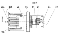
図1は本発明によるキャン型の光モジュールの第1の実施例を示す一部断面側面図である。図2は図1中に示したLD基板を中心としたCAN内部の平面図である。
図1及び図2に示すように、ベース21を貫通した配線基板22と放熱基板24の先端にメイン基板25が接続され、このメイン基板25の上に、半導体レーザダイオード(LD)11、サブマウント式中継基板27に搭載されたモニタフォトダイオード(モニタPD)12等が、はんだ付けされる。放熱基板24上にはドライバIC14がはんだ付けされる。また、貫通した配線基板22の後方にはフラットリード端子23が接続されている。フラットリード端子23としては、光軸に沿った後方には主に、高周波信号用リード端子23aが接続され、リード端子数が不足する場合には、配線基板22の側面からも、高周波信号用リード端子23aと同様の光軸方向になるように曲げられた折れ曲がりリード端子23b、23cが接続される。
【0010】
ここで、メイン基板上25上に搭載されたLD11とモニタPD12との関係を説明する。モニタPD12は、その受光面がほぼZ軸方向に向くように、LD11後方面に位置するサブマウント式中継基板27に搭載される。LD11の後方光は直接入力モニタPD12に入力されるため、入射光量は十分確保される。なお、モニタPD12が完全にZ軸方向を向いているのでは無く、X軸方向にわずかに傾斜しているのは、モニタPD12表面での反射光がLD11に戻らないようにするためである。ここで、サブマウント式中継基板27のX軸上面はインピーダンス整合された配線路を有した構造としているため、LD11からドライバIC14まで、短い距離で高周波特性の良い接続が可能であり、搭載面積を少なくすることが可能となる。また、ドライバIC14は放熱基板24上に直接接続される構造のため、放熱性も確保される。74は本発明によって設けられた絞り部であり、これについては、詳細後述する。
【0011】
また、レンズ15が予め付けられたレンズホルダ16はLD11に対して調芯した後、ベース21に溶接等で固定される。レンズホルダ16に対して、ファイバガイド56に入れられたファイバフェルール51をXYZ方向に調芯し、YAG溶接等で固定する。最後にレセプタクル部55をファイバフェルール51に取り付けて、レセプタクル型光モジュールが完成する。光出力の調整や実使用時には着脱用光ファイバフェルール54がレセプタクル部55に挿入され、光出力が得られる状態となる。
ところで、一般に、ドライバICを内蔵して直接変調する方式の光モジュールは、高周波応答を良くするため、すなわち光波形のアイの開口をなるべく大きくするために、LDに対する駆動電流を大きくする傾向が強い。この結果、光ファイバからの出力光量の規格に対して、LDの発光パワーに余裕がある場合が多い。そのため、光ファイバに入力される光量を減衰調節する方法として、ファイバフェルール51に入射される光量をアイソレータ53を矢印61のように左右に回転して調整したり、ファイバフェルール51全体を矢印62のように光軸方向の前後に移動させたりしてデフォーカスさせて調整する方法が適用できる。
【0012】
次に、図1に示す1枚レンズ系での結像関係を、図3を用いて説明する。
図3は図1に示す1枚レンズの光結合系を説明するための模式図である。なお、以下の図において、同じ構成要素に対しては同一の符号を付けてその説明を省略する。
一般にLD11のスポット直径は2ミクロン弱で、シングルモードファイバの場合、ファイバコア57のモードフィールド直径は8〜10ミクロン程度のため、結合効率を最適化したレンズ系では、その像倍率は4〜6倍のことが多い。つまり、LD11とレンズ15を模式的に表現したレンズ41間の距離をL1とし、レンズ41とファイバフェルール51の入射面との距離をL2とすると、レンズ41とファイバフェルール51との距離L2はL1の4〜6倍になる。一般にシングルモードファイバの開口数NAは0.1程度であり、レンズ41のファイバ側の開口数は0.1程度に一致するように設計されている。この結果、前述の像倍率より、レンズ41のLD側の開口数は0.4〜0.6と設計することが望ましい。球面レンズでは、レンズの収差のため、上記のような開口数の関係にならない場合もあるが、標準的に市販されており、レンズ収差の補正された非球面レンズでは、一般に上記のような開口数の関係になるように設計されている。ちなみに、図3に示すように、LD11から出射されたレーザビームの出射角をθLとし、レンズ41から出射されたレーザビームがファイバフェルール51の入射面に入射される角度をθfとすると、LD側のレンズの開口数NA=sinθLで、ファイバ側のレンズの開口数NA=sinθfで規定される。ファイバ側のレンズの有効直径をDとすると、ファイバ側のレンズの開口数NAは0.1程度のため、近似して、NA=sinθf≒tanθf=D/2/L2と表すことができる。
【0013】
次に、光モジュール全体が室温より、高い温度で使用される状態について説明する。一般にレンズホルダ16は、溶接等の接合性を考慮し、ステンレス等の金属で作られることが多く、その熱膨張係数は10〜20ppm/℃程度である。一方、配線基板22とメイン基板25はセラミック系の材料で配線線路を形成しており、その熱膨張係数は4〜8ppm/℃程度である。放熱基板24は配線基板22と熱膨張係数をほぼ一致させた放熱性の良い、例えばCuW等の金属で構成される。以上のように、レンズホルダ16と基板を熱膨張係数の近い材質で構成することは困難である。この結果、室温より高い温度で使用される場合、熱膨張係数の比較的大きいレンズホルダ16は図1のBLE部分が膨張し、熱膨張係数の比較的小さい配線基板22とメイン基板25は図1のBLD部分が膨張するため、その差のΔL1だけ、LD11とレンズ15との間隔は伸びることになる。この状態を模式的に図4に示す。
【0014】
図4は図1に示す1枚レンズの光結合系における温度によるレンズの移動を説明するための模式図である。上記のように、温度が上昇した場合にレンズ41が右側、即ちファイバフェルール51側にΔL1だけ移動し、レンズ42として配置されている状態が示されている。レンズ41がΔL1だけ、ファイバフェルール51側に移動した結果、ファイバフェルール51側のビームウェスト43はΔL2だけ、レンズ側に移動する。前述したように、レンズの光学系の像倍率は4〜6倍のことが多い。ΔL2はΔL1の(光学倍率)の2乗となるため、ΔL1が1〜2ミクロン弱でも、ΔL2は、16〜50ミクロン程度の範囲で変動することになるため、光結合効率の大きな変動が発生する。
【0015】
図5はビームウェスト位置の変化に対する結合効率の変化を示す特性図であり、横軸はファイバフェルールの入射面からビームウェスト43間の距離L3(μm)、すなわち、前述のデフォーカス量を示す。縦軸は結合効率(dB)を示す。温度が上昇すると、ビームウェスト43は図4に向かって左側に移動する。逆に、温度が下がると、ビームウェスト43は右側に移動する。
図において、曲線71は、図1において絞り部74がない場合の、ファイバフェルール51の入射面からビームウェスト43間の距離L3(μm)に対する結合効率(dB)を示しており、常温より高温になった場合、ΔL2の16〜50ミクロン程度の変動に対しての結合効率の変化が確認できる。例えば、前述のように、入射光量をアイソレータ53の回転61で調整する場合には、ビームウェスト43がファイバフェルール51の入射面にある場合、即ちL3が0ミクロンの場合、L3が最大+50ミクロン程度の変動すると、結合効率は約0.5dB弱ぐらい変動する。また、ファイバフェルール51全体を矢印62に示すように光軸方向に移動させてデフォーカスにより調整する場合には、組立時に仮に−2dBのデフォーカスを与えると(つまり、L3が+約100μmになるようにすると)、最大50ミクロン程度の変動は1.5dB程度の変動に相当する。なお、曲線72はレンズ41の入射面に絞りが設けられた場合の結合効率を示しており、これについては、後述する。
以上のように、ΔL2変動に対して光量の変動が大きく発生する。即ち、温度上昇によってファイバフェルール51の入射面に入射される入射光量が変動し、光結合効率の変動が発生する。
【0016】
そこで、図6を用いて、レンズ41の前方に絞り73を付加することにより、光結合効率の変動を防止する方法を説明する。
図6はレンズの前に絞りを形成した場合の光学系について説明するための模式図である。図において、点線で示される絞り無い場合のビームプロファイル81は、レンズ41の開口数NAに応じて決まる。実線で示される絞り73が有る場合のビームプロファイル82は、絞り73の穴径で決まり、レンズ41の開口数NAが小さくなった分だけ、回折限界が悪くなり、ビームウェスト径が大きくなる。言い換えると、ビームプロファイル82は寸胴気味になり、図1のZ方向におけるビーム径の変化が小さくなる。
このため、レンズの入射面に絞りを設けると、図5の曲線72のように、ビームウェスト43のΔL2変動に対して光量の変動が小さくなり、光結合効率の変動を大きく低減できる。
【0017】
次に、絞りの大きさとレンズに対する位置精度について説明する。
図7はレンズと絞りの一部断面側面図であり、レンズに対して絞りに位置ずれが生じた場合をしめしている。図7に示すように、レンズ15のLD側(絞り73の有る側)のレンズ有効直径をDとし、絞り73の穴直径をdとし、レンズ15の中心に対する絞り73の中心のずれをd1とする。
【0018】
図8はレンズ開口数NAに対する結合効率及びビーム径比を示す特性図であり、横軸にレンズ開口数NAを示し、第1の縦軸は結合効率を示し、第2の縦軸はビーム径比を示す。ビーム径比とは、絞り73がない場合のビームウェスト43のビーム径を1とし、絞り73を設けた場合のビームウェスト43の径をrとした場合のrをいう。
図において、曲線41はLD側のレンズ15の開口数を0.4と仮定し、絞りを付加して開口数を小さくした場合の結合効率を示し、曲線51はビーム径比を示す。絞りの穴径を小さくして開口数を小さくした場合には、結合効率は低下するが、ビーム直径は絞りの無い場合に比べて大きくできる。しかし、絞りを付加したことによる結合効率の極端な低下は避けるべきであり、−5〜−7dB程度が限界と考えられる。この場合、LD側レンズの開口数は0.2以上であり、ビーム径の拡大率も2倍以内となる。絞りの無い場合のファイバフェルール51側のレンズの開口数は0.1であり、絞りを付加した場合の開口数は0.05以上となる。
【0019】
実際には、結合効率の減衰量に依存するが、結合効率が極端に低下せず、ビーム径が拡大できるのは、レンズの開口数で0.25〜0.35程度が望ましいと考えられる。つまり、レンズ15に絞り73を接近させて配置した場合は、絞りの穴直径dをレンズ有効直径Dの0.25/0.4〜0.35/0.4、つまり63〜88%程度に設定すれば良い。この場合、ファイバ側のレンズの開口数は0.063〜0.088程度に設定すれば良い。
【0020】
次に、レンズと絞りの中心ずれについて、図7、9を用いて説明する。
図9は絞りの中心がレンズ中心に対してずれた場合の結合効率を示す特性図である。絞り73の中心とレンズ15の中心のずれをd1とし、絞り73の直径をdとした場合、横軸はd1/dを示す。縦軸は結合効率(dB)を示す。図7に示すように、レンズ15の中心に対する絞り穴の中心ずれを規定した場合、絞り直径dに対する中心ずれ量d1、即ちd1/dに対して、結合効率は図9のようになる。結合効率の極端な低下は回避すべきであり、仮に結合効率が−1dB程度以内とした場合、d1/dは絞り直径は略0.35(即ち35%)となるので、d1/dは略0.35に抑えることが望ましい。
レンズ15の有効直径D=1000ミクロン、絞りの穴直径d=500ミクロンとした場合、中心ずれの許容値は500x0.35=175ミクロンであり、通常の光モジュールの加工組立精度から考慮して、問題とならないことがわかる。
【0021】
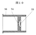
次に、実際の絞りの構造を図10に示す。
図10は図1に示した絞り部の第1の実施例を示す拡大断面図である。図に示すように、本実施例では、レンズ15を付けるレンズホルダ16に絞り穴を設けて絞り部74としているため、絞り部74は容易に実現できる。ここで、絞りを配置する位置は、レンズ15の直前直後に限らず、LDとファイバ間の任意の位置に配置できることは言うまでもない。但し、レンズ15の直前直後に配置する場合以外は、絞りの穴径を小さくして、レンズ中心と絞り中心の合わせ精度を厳しくしなければならないので、レンズの直前、もしくは直後に絞りを配置する構造の方が望ましい。
【0022】
図11は本発明による光モジュールの絞り部の第2の実施例を示す断面図である。図11に示すように、絞り部品77を別部品として製作しておき、絞り部品77を絞りの無いレンズホルダ76のLD側に溶接や接着等で接合する構造としている。
【0023】
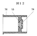
図12は本発明による光モジュールの絞り部の第3の実施例を示す断面図である。図12に示すように、絞り部品78を別部品として製作しておき、絞りの無いレンズホルダ76のファイバフェルール51側に絞り部品78を接合する構造としてもよい。
【0024】
また、以上のようにレンズに絞りを付加する方法では無く、レンズそのものの有効径を小さくする方法について、図13をもちいて説明する。
図13は本発明による光モジュールの絞り効果を有するレンズの一実施例を示す側面図である。図に示すように、レンズ15aの入射面の外縁79を削除したり、表面形状を荒らす等して変えたりする。また、レンズ15aの入射面の代わりに、レンズ15aの出射面の外縁79を削除したり、表面形状を荒らしたりしてもよい。レンズ15aをこのように構成すると、レンズ15aの周辺部のレンズ効果が無くなるので、あたかも絞り部を設けたのと同じ効果を有する。よって、本発明では、これを絞り効果という。レンズ外縁79を削除することは、元のレンズ有効径Dを小さくしてレンズ有効径Dnとしたものと同等の効果を有する。前述のように、ファイバ側のレンズの開口数=0.1程度の場合、ファイバ側のレンズの有効径Dは、NA=0.1=D/2/L2より、D=0.2×L2である。これに対して、前述のように、NAを0.05以上、0.1未満にして、絞りの効果を有するには、ファイバ側のレンズの有効径Dnを、0.1×L2≦Dn<0.2×L2に設定すればよい。
本実施例では、レンズの金型を新規に製作する手間とコストは必要であるが、絞りを付加した場合と同様の効果が得られることは言うまでもない。
【0025】
次に、本発明の光モジュールを用いた光伝送モジュール(又は、光トランシーバ)の構成及び動作について説明する。
図14は本発明による光伝送モジュールの一実施例を示す斜視図であり、レセプタクル型光伝送モジュールを示す。送信モジュール1は、前述の構造で、別途組み立てられ、フラットリード端子2とレセプタクル型光コネクタ3を有した構造となっている。また、受信モジュール4も、フラットリード端子5とレセプタクル型光コネクタ6を有した構造となっている。
【0026】
まず、固定部95にプリント基板91を位置決めする。なお、プリント基板91上には、電気信号制御IC94等が面付け実装されており、外部との電気信号は、カードエッジ部93の配線を介して送受信される。送信モジュール1のフラットリード端子2を、プリント基板91上の電極パッド92に重ね合わせて、リードピン2をはんだ固定する。同様に受信モジュール4も、プリント基板91にリードピン5を介してはんだ固定する。ここで、それぞれのはんだ固定時に、プリント基板91に対して、レセプタクル型光コネクタ3、6の位置が許容値以内になるようにするため、電極パッド92とフラットリード2、5の位置関係を調整する必要がある。
【0027】
光伝送モジュールにおいて、光軸方向の組立公差が最も緩いため、光モジュールとの電気接続部の光軸方向の位置ずれ量が大きくなる。キャン型光モジュールをプリント基板91に対して、光軸方向のみにリードを伸ばした構造にしたため、電極パッド92に対して光軸方向に前後して、光コネクタの位置は最大ミリメータオーダで位置調整が可能となる。以上により、レセプタクル部が付いている光モジュールと、プリント基板を別々に製作後、その位置関係を調整しながら接続することが可能となる。これにより、光送受信モジュールとプリント基板部の位置ずれを吸収し、光トランシーバの外形に対して、電気信号用コネクタのリードピンやカードエッジの位置と光コネクタの位置を規定した状態で組立可能となる。
【0028】
次に、図15を用いて、箱型の光モジュールを用いた場合について説明する。図15は箱型の光モジュールの一実施例を示す斜視図である。図に示すように、箱型の光モジュールとは箱にフラットリード端子102が接続された構造をいい、通常バタフライ型の光モジュールと呼ぶこともある。バタフライ型の光モジュールとは、箱型のパッケージの内部に光素子やレンズを位置決めして搭載後、箱の側面にレンズや光ファイバを固定する構造をいう。箱型光モジュール101も、フラットリード端子102と、レセプタクル型光コネクタ103を有した構造をしており、前述のキャン型同様に、プリント基板91に搭載可能であり、本発明によって、温度変化による結合効率を改善することができる。
【0029】
以上述べたように、本実施例では、レンズの前後に絞り部を設けたり、レンズの外縁を光が通らないように加工したりすることによって、温度変化による結合効率の劣化を改善している。レンズの外縁を加工して、レンズの外縁を光が通過しないようにすることは、レンズ自身に絞り部を設けたのと同じことであるので、レンズ自身を加工して絞り効果を持たせた場合には、絞りを設けるという。
【0030】
以上述べたように、本発明によれば、光モジュールの内部に、送信モジュールであればLDのドライバICを内蔵することにより、サイズが大きくなって、熱膨張により光素子とレンズの間隔が変化しやすくなった場合にも、絞りを入れることにより、光パワーの変動を抑え、光結合効率の変動等を防止できる。以上より、低コストで製作できる光モジュール、光伝送モジュール(又は光トランシーバ)を提供することが可能になる。
【0031】
【発明の効果】
以上述べたように、光パワーの変動を抑え、光結合効率の変動を防止できる。
【図面の簡単な説明】
【図1】本発明によるキャン型の光モジュールの第1の実施例を示す一部断面側面図である。
【図2】図1中に示したLD基板を中心としたCAN内部の平面図である。
【図3】図1に示す1枚レンズの光結合系を説明するための模式図である。
【図4】図1に示す1枚レンズの光結合系における温度によるレンズの移動を説明するための模式図である。
【図5】図5はビームウェスト位置の変化に対する結合効率の変化を示す特性図である。
【図6】レンズの前に絞りを形成した場合の光学系について説明するための模式図である。
【図7】レンズと絞りの一部断面側面図である。
【図8】レンズ開口数NAに対する結合効率及びビーム径比を示す特性図である。
【図9】絞りの中心がレンズ中心に対してずれた場合の結合効率を示す特性図である。
【図10】図1に示した絞り部の第1の実施例を示す拡大断面図である。
【図11】本発明による光モジュールの絞り部の第2の実施例を示す断面図である。
【図12】本発明による光モジュールの絞り部の第3の実施例を示す断面図である。
【図13】本発明による光モジュールの絞り効果を有するレンズの一実施例を示す側面図である。
【図14】本発明による光伝送モジュールの一実施例を示す斜視図である。
【図15】箱型の光モジュールの一実施例を示す斜視図である。
【符号の説明】
1…送信モジュール、2…フラットリード端子、3…レセプタクル型光コネクタ、4…受信モジュール、5…フラットリード端子、6…レセプタクル型光コネクタ、11…半導体レーザダイオード、12…モニタフォトダイオード(モニタPD)、14…ドライバIC、15…レンズ、16…レンズホルダ、21…ベース、22…配線基板、23…リード端子、24…放熱基板、25…メイン基板、27…サブマウント式中継基板、41…レンズ、42…レンズ、43…ビームウェス、51…ファイバフェルール、53…アイソレータ、54…着脱用光ファイバフェルール、55…レセプタクル部、56…ファイバガイド、57…ファイバコア、65…入射光、73…絞り、74…絞り部、76…レンズホルダ、77…絞り、78…絞り、81…絞り無い場合のビームプロファイル、82…絞り有る場合のビームプロファイル、91…プリント基板、92…電極パッド、93…カードエッジ部、94…電気制御用IC、95…固定部、101…箱型光モジュール、102…フラットリード端子、103…レセプタクル型光コネクタ。[0001]
BACKGROUND OF THE INVENTION
The present invention relates to a technique for improving the temperature characteristics of an optical transmission module, and is particularly suitable for application to a can-type optical module.
[0002]
[Prior art]
In an optical communication module using an optical fiber, a laser diode (hereinafter abbreviated as LD) as a light emitting element and a photodiode (hereinafter abbreviated as PD) as a light receiving element are housed in various packages from the viewpoint of reliability. Among these packages, there is a can-type package that can easily have a coaxial structure with an optical fiber. This can package is often used for a receptacle-type optical transmission module in which an optical fiber is inserted and removed (see, for example, Patent Document 1).
[0003]
[Patent Document 1]
JP 2001-66468 A
[0004]
[Problems to be solved by the invention]
2. Description of the Related Art In recent years, optical transmission modules (or optical transceivers) in which a transmission module incorporating an LD, a reception module incorporating a PD, an electric signal control IC, and the like are integrated are becoming smaller and faster. In a small optical transmission module, a receptacle-type optical module is often used in order to have a structure in which an optical connector can be inserted and removed, and the above-described can-type optical module is used at a communication speed of 2.5 Gbit / s or less. There are many.
On the other hand, in order to increase the speed of 10 Gbit / s or more, it is desirable to incorporate an LD driver IC in the case of a transmission module and a PD preamplifier IC in the case of a reception module. For this reason, it is difficult to incorporate a driver IC and a preamplifier IC in a can of the same size as a conventional optical module for communication speed of 2.5 Gbit / s or less. To incorporate these, it is necessary to increase the diameter and length of the can.
In addition, since the can type optical module has a structure in which a metallic holder with a lens is bonded onto a substrate on which an optical element is mounted, the diameter and length of the can increase. When the diameter or length of the can increases, the distance between the optical element and the lens is likely to change due to thermal expansion, which causes a problem that the fluctuation of the optical power tends to increase.
A similar problem occurs in a butterfly type optical module in which terminals are provided on several sides of the housing, although there are some differences.
[0005]
An object of the present invention is to provide a technique capable of suppressing fluctuations in optical power due to thermal expansion even when a driver IC or a preamplifier IC is incorporated and an optical transmission module having a transmission module and a reception module is enlarged. There is.
[0006]
[Means for Solving the Problems]
In order to achieve the above object, in the first invention, the light transmission module receives a laser diode that emits laser light, a lens for condensing the laser light, and laser light emitted from the lens. A fiber ferrule having a fiber core, and a diaphragm provided at the lens itself, before the lens, or after the lens, and the distance between the laser diode and the lens varies depending on the temperature, and is coupled with the fiber ferrule. Improve efficiency degradation.
[0007]
In the second invention, the optical transmission module includes a base, a laser diode mounted on a substrate fixed to the base, and a lens holder for condensing the laser light, and the lens holder fixed to the base A fiber ferrule having a fiber core to which the laser light emitted from the lens is incident, and a diaphragm provided in front of the lens or in front of the lens, or after the lens, and the laser diode and the lens The interval varies with temperature, and the coupling efficiency with the fiber ferrule is improved.
[0008]
DETAILED DESCRIPTION OF THE INVENTION
Hereinafter, embodiments of the present invention will be described with reference to the drawings using some examples.
Among optical modules, in particular, the can-type optical module has a structure in which a metallic holder with a lens is bonded onto a metal substrate on which an optical element is mounted. The interval of becomes easy to change. Along with this, there is a problem that the fluctuation of the optical power tends to increase. An embodiment of a structure that prevents this will be described with reference to FIGS.
The can-type optical module can be called a coaxial structure in a broad sense. The coaxial structure refers to a structure in which a lens and an optical fiber are sequentially stacked and fixed on an optical element mounted on a coaxial can package.
[0009]
FIG. 1 is a partial sectional side view showing a first embodiment of a can-type optical module according to the present invention. FIG. 2 is a plan view of the inside of the CAN with the LD substrate shown in FIG. 1 as the center.
As shown in FIGS. 1 and 2, a
[0010]
Here, the relationship between the LD 11 mounted on the
[0011]
The
By the way, in general, an optical module of a type that directly modulates with a built-in driver IC has a strong tendency to increase the drive current for the LD in order to improve the high-frequency response, that is, to increase the eye opening of the optical waveform as much as possible. . As a result, the light emission power of the LD often has a margin with respect to the standard of the amount of light output from the optical fiber. Therefore, as a method for adjusting the attenuation of the amount of light input to the optical fiber, the amount of light incident on the
[0012]
Next, the imaging relationship in the single lens system shown in FIG. 1 will be described with reference to FIG.
FIG. 3 is a schematic diagram for explaining the optical coupling system of the single lens shown in FIG. In the following drawings, the same components are denoted by the same reference numerals and description thereof is omitted.
In general, the spot diameter of the
[0013]
Next, a state where the entire optical module is used at a temperature higher than room temperature will be described. In general, the
[0014]
FIG. 4 is a schematic diagram for explaining the lens movement due to temperature in the single lens optical coupling system shown in FIG. As described above, when the temperature rises, the
[0015]
FIG. 5 is a characteristic diagram showing the change in coupling efficiency with respect to the change in beam waist position, and the horizontal axis shows the distance L3 (μm) between the
In the figure, a
As described above, the light amount greatly varies with respect to the ΔL2 variation. That is, the amount of incident light that is incident on the incident surface of the
[0016]
A method for preventing fluctuations in the optical coupling efficiency by adding a
FIG. 6 is a schematic diagram for explaining an optical system when a stop is formed in front of a lens. In the figure, the
For this reason, when a stop is provided on the entrance surface of the lens, as shown by a
[0017]
Next, the size of the stop and the positional accuracy with respect to the lens will be described.
FIG. 7 is a partial cross-sectional side view of the lens and the stop, and shows a case where the position shift occurs in the stop with respect to the lens. As shown in FIG. 7, the lens effective diameter of the
[0018]
FIG. 8 is a characteristic diagram showing the coupling efficiency and the beam diameter ratio with respect to the lens numerical aperture NA. The horizontal axis represents the lens numerical aperture NA, the first vertical axis represents the coupling efficiency, and the second vertical axis represents the beam diameter. Indicates the ratio. The beam diameter ratio refers to r when the beam diameter of the
In the figure,
[0019]
Actually, although it depends on the attenuation amount of the coupling efficiency, it is considered that it is desirable that the beam diameter can be expanded without extremely reducing the coupling efficiency and the numerical aperture of the lens is about 0.25 to 0.35. That is, when the
[0020]
Next, the center deviation between the lens and the aperture will be described with reference to FIGS.
FIG. 9 is a characteristic diagram showing the coupling efficiency when the center of the stop is shifted from the center of the lens. When the shift between the center of the
When the effective diameter D of the
[0021]
Next, an actual aperture structure is shown in FIG.
FIG. 10 is an enlarged sectional view showing a first embodiment of the aperture shown in FIG. As shown in the drawing, in the present embodiment, the
[0022]
FIG. 11 is a sectional view showing a second embodiment of the stop portion of the optical module according to the present invention. As shown in FIG. 11, the
[0023]
FIG. 12 is a sectional view showing a third embodiment of the aperture portion of the optical module according to the present invention. As shown in FIG. 12, the
[0024]
In addition, a method of reducing the effective diameter of the lens itself, not the method of adding a diaphragm to the lens as described above, will be described with reference to FIG.
FIG. 13 is a side view showing an embodiment of a lens having a diaphragm effect of the optical module according to the present invention. As shown in the figure, the
In this embodiment, it takes time and cost to newly manufacture a lens mold, but it goes without saying that the same effect as that obtained when a diaphragm is added can be obtained.
[0025]
Next, the configuration and operation of an optical transmission module (or optical transceiver) using the optical module of the present invention will be described.
FIG. 14 is a perspective view showing an embodiment of an optical transmission module according to the present invention, and shows a receptacle type optical transmission module. The
[0026]
First, the printed
[0027]
In the optical transmission module, since the assembly tolerance in the optical axis direction is the loosest, the amount of positional deviation in the optical axis direction of the electrical connection portion with the optical module increases. Since the can-type optical module has a structure in which the leads are extended only in the optical axis direction with respect to the printed
[0028]
Next, a case where a box-type optical module is used will be described with reference to FIG. FIG. 15 is a perspective view showing an embodiment of a box-type optical module. As shown in the figure, a box-type optical module refers to a structure in which a
[0029]
As described above, in this embodiment, the deterioration of the coupling efficiency due to the temperature change is improved by providing a diaphragm part before and after the lens or by processing so that light does not pass through the outer edge of the lens. . Processing the outer edge of the lens so that light does not pass through the outer edge of the lens is the same as providing a diaphragm on the lens itself, so the lens itself was processed to have a diaphragm effect. In some cases, a diaphragm is provided.
[0030]
As described above, according to the present invention, by incorporating a driver IC of an LD in the case of a transmission module inside the optical module, the size increases, and the distance between the optical element and the lens changes due to thermal expansion. Even when it becomes easy to perform, it is possible to suppress the fluctuation of the optical power and prevent the fluctuation of the optical coupling efficiency by inserting the aperture. As described above, it is possible to provide an optical module and an optical transmission module (or an optical transceiver) that can be manufactured at low cost.
[0031]
【The invention's effect】
As described above, fluctuations in optical power can be suppressed and fluctuations in optical coupling efficiency can be prevented.
[Brief description of the drawings]
FIG. 1 is a partial sectional side view showing a first embodiment of a can-type optical module according to the present invention.
FIG. 2 is a plan view of the inside of the CAN with the LD substrate shown in FIG. 1 as a center.
3 is a schematic diagram for explaining an optical coupling system of the single lens shown in FIG. 1. FIG.
FIG. 4 is a schematic diagram for explaining lens movement due to temperature in the single lens optical coupling system shown in FIG. 1;
FIG. 5 is a characteristic diagram showing a change in coupling efficiency with respect to a change in beam waist position.
FIG. 6 is a schematic diagram for explaining an optical system when a stop is formed in front of a lens.
FIG. 7 is a partial cross-sectional side view of a lens and a diaphragm.
FIG. 8 is a characteristic diagram showing coupling efficiency and beam diameter ratio with respect to lens numerical aperture NA.
FIG. 9 is a characteristic diagram showing coupling efficiency when the center of the stop is shifted from the center of the lens.
FIG. 10 is an enlarged cross-sectional view showing a first embodiment of the aperture shown in FIG. 1;
FIG. 11 is a cross-sectional view showing a second embodiment of the aperture portion of the optical module according to the present invention.
FIG. 12 is a cross-sectional view showing a third embodiment of the aperture portion of the optical module according to the present invention.
FIG. 13 is a side view showing an embodiment of a lens having a diaphragm effect of the optical module according to the present invention.
FIG. 14 is a perspective view showing an embodiment of an optical transmission module according to the present invention.
FIG. 15 is a perspective view showing an embodiment of a box-type optical module.
[Explanation of symbols]
DESCRIPTION OF
Claims (6)
前記基板と前記レンズホルダとは、互いに熱膨張係数が相違し、
前記レンズの有効径を前記レンズと前記ファイバコア間の距離の0.1倍以上、0.2倍未満にしたことを特徴とする光伝送モジュール。 A main board mounted on one end of the heat radiating board; a wiring board mounted on one end of the heat radiating board; and a main board mounted on the other end of the heat radiating board. A laser diode mounted on the circuit board, an IC mounted between the wiring board and the main board of the heat dissipation board and electrically connected to the wiring board and the laser diode, and a laser from the laser diode A lens holder, which is mounted with a lens for condensing light , is fixed at one end to the base and extends in the optical axis direction, and a fiber ferrule having a fiber core on which the laser light emitted from the lens is incident In an optical transmission module having
The substrate and the lens holder have different coefficients of thermal expansion,
An optical transmission module, wherein an effective diameter of the lens is 0.1 times or more and less than 0.2 times a distance between the lens and the fiber core.
前記ファイバフェルール側のレンズの開口数が0.05以上0.1未満であることを特徴とする光伝送モジュール。The optical transmission module according to claim 1,
An optical transmission module, wherein a numerical aperture of a lens on the fiber ferrule side is 0.05 or more and less than 0.1.
前記レンズと前記ファイバフェルールの間に、前記レンズに入射される光量について、偏光子を光軸回りに回転することにより調整可能なアイソレータを配置することを特徴とする光伝送モジュール。The optical transmission module according to claim 1 or 2,
An optical transmission module, wherein an isolator capable of adjusting a light amount incident on the lens by rotating a polarizer around an optical axis is disposed between the lens and the fiber ferrule.
前記ファイバフェルールに入射される光量が、前記ファイバフェルールを光軸方向に前後してデフォーカスされたことを特徴とする光伝送モジュール。The optical transmission module according to claim 1 or 2,
An optical transmission module, wherein the amount of light incident on the fiber ferrule is defocused by moving the fiber ferrule back and forth in the optical axis direction.
前記レーザダイオードから前記ファイバコアに至る光軸に平行な貫通基板上に前記レーザダイオードが実装されたキャン型光モジュールを備えることを特徴とする光伝送モジュール。The optical transmission module according to any one of claims 1 to 4,
An optical transmission module comprising a can-type optical module in which the laser diode is mounted on a through substrate parallel to an optical axis from the laser diode to the fiber core.
リードピンをさらに設け、前記リードピンの全てを前記レーザダイオードから前記ファイバコアに至る光軸の延在方向に伸ばした構造とすることを特徴とする光伝送モジュール。The optical transmission module according to any one of claims 1 to 5,
An optical transmission module comprising: a lead pin; and a structure in which all of the lead pins are extended in an extending direction of an optical axis from the laser diode to the fiber core.
Priority Applications (2)
| Application Number | Priority Date | Filing Date | Title |
|---|---|---|---|
| JP2002304040A JP3950779B2 (en) | 2002-10-18 | 2002-10-18 | Optical transmission module |
| US10/631,389 US7037000B2 (en) | 2002-10-18 | 2003-07-30 | Optical transmission module |
Applications Claiming Priority (1)
| Application Number | Priority Date | Filing Date | Title |
|---|---|---|---|
| JP2002304040A JP3950779B2 (en) | 2002-10-18 | 2002-10-18 | Optical transmission module |
Publications (2)
| Publication Number | Publication Date |
|---|---|
| JP2004138864A JP2004138864A (en) | 2004-05-13 |
| JP3950779B2 true JP3950779B2 (en) | 2007-08-01 |
Family
ID=32451589
Family Applications (1)
| Application Number | Title | Priority Date | Filing Date |
|---|---|---|---|
| JP2002304040A Expired - Lifetime JP3950779B2 (en) | 2002-10-18 | 2002-10-18 | Optical transmission module |
Country Status (2)
| Country | Link |
|---|---|
| US (1) | US7037000B2 (en) |
| JP (1) | JP3950779B2 (en) |
Families Citing this family (17)
| Publication number | Priority date | Publication date | Assignee | Title |
|---|---|---|---|---|
| US7364367B2 (en) * | 2003-12-25 | 2008-04-29 | Matsushita Electric Industrial Co., Ltd. | Optical module manufacturing method and optical module |
| US7121741B2 (en) * | 2004-10-26 | 2006-10-17 | Konica Minolta Holdings, Inc. | Optical communication module |
| JP2008170636A (en) * | 2007-01-10 | 2008-07-24 | Nec Electronics Corp | Semiconductor laser module |
| JP4770796B2 (en) * | 2007-05-31 | 2011-09-14 | ブラザー工業株式会社 | Light source device, exposure device, and image forming apparatus |
| JP4698666B2 (en) * | 2007-12-28 | 2011-06-08 | 日本オプネクスト株式会社 | Optical transceiver module |
| JP2010278285A (en) * | 2009-05-29 | 2010-12-09 | Renesas Electronics Corp | Method of manufacturing optical receiver module, and apparatus for manufacturing the same |
| WO2011145652A1 (en) * | 2010-05-19 | 2011-11-24 | 塩野義製薬株式会社 | Defocused optical rotation measurement apparatus, optical rotation measurement method and defocused optical fiber system |
| TW201239336A (en) * | 2010-11-26 | 2012-10-01 | Global Fiberoptics Ltd | Optical rotation measurement device, polarization conversion optical system that can be used for optical rotation measurement, and method for measuring optical rotation in optical rotation measurement system using said polarization conversion optical |
| JP2015106577A (en) * | 2013-11-28 | 2015-06-08 | 三菱電機株式会社 | Semiconductor package for optical communication |
| JP6340902B2 (en) * | 2014-05-13 | 2018-06-13 | 住友電気工業株式会社 | Manufacturing method of optical module |
| US9780882B2 (en) * | 2014-05-13 | 2017-10-03 | Sumitomo Electric Industries, Ltd. | Optical transmitter module having multiple signal lanes |
| JP2016091024A (en) * | 2014-10-31 | 2016-05-23 | 住友電気工業株式会社 | Light-emitting module and multichannel light-emitting module |
| JP2016220094A (en) * | 2015-05-22 | 2016-12-22 | 日本電気株式会社 | Optical transceiver |
| KR101985016B1 (en) * | 2017-09-22 | 2019-09-03 | 주식회사 포벨 | Optical Device Capable of Fine Tuning of Output Power And Manufacturing Method Thereof |
| US10451810B1 (en) * | 2018-08-22 | 2019-10-22 | Corning Optical Communications LLC | Adapter for electrically connecting a laser diode to a circuit board |
| WO2020189829A1 (en) * | 2019-03-21 | 2020-09-24 | 김정수 | Optical device capable of precise adjustment of optical output intensity, and method for manufacturing optical device |
| JP7303457B2 (en) * | 2019-09-18 | 2023-07-05 | 日本電信電話株式会社 | Optical module package |
Family Cites Families (7)
| Publication number | Priority date | Publication date | Assignee | Title |
|---|---|---|---|---|
| JP3770945B2 (en) * | 1995-10-31 | 2006-04-26 | 富士通株式会社 | Optical device having optical film with variable incident angle |
| JP3495493B2 (en) | 1996-02-07 | 2004-02-09 | アルプス電気株式会社 | Light emitting module |
| JPH09218324A (en) | 1996-02-08 | 1997-08-19 | Alps Electric Co Ltd | Light emission module |
| JP2001066468A (en) | 1999-08-27 | 2001-03-16 | Hitachi Cable Ltd | Optical receptacle |
| WO2001043245A1 (en) * | 1999-12-10 | 2001-06-14 | Sumitomo Electric Industries, Ltd. | Optical semiconductor module |
| JP3813496B2 (en) * | 2000-12-20 | 2006-08-23 | 古河電気工業株式会社 | Optical connector |
| DE10112274B4 (en) * | 2001-03-14 | 2006-05-24 | Finisar Corp.(N.D.Ges.D.Staates Delaware), Sunnyvale | Optoelectronic transmission module and method for its production |
-
2002
- 2002-10-18 JP JP2002304040A patent/JP3950779B2/en not_active Expired - Lifetime
-
2003
- 2003-07-30 US US10/631,389 patent/US7037000B2/en not_active Expired - Fee Related
Also Published As
| Publication number | Publication date |
|---|---|
| JP2004138864A (en) | 2004-05-13 |
| US20040114883A1 (en) | 2004-06-17 |
| US7037000B2 (en) | 2006-05-02 |
Similar Documents
| Publication | Publication Date | Title |
|---|---|---|
| JP3950779B2 (en) | Optical transmission module | |
| US6155724A (en) | Light transmitting module for optical communication and light transmitting unit thereof | |
| US11360279B2 (en) | Optical subassembly and optical module | |
| US20110317965A1 (en) | Optical subassembly with optical device having ceramic package | |
| JP3488159B2 (en) | Alignment device for light source and optical fiber and light source module having the same | |
| WO2004008593A1 (en) | Package for optical semiconductor | |
| US11129279B2 (en) | Optical subassembly and optical module | |
| US20090274421A1 (en) | Optical semiconductor module, adjusting method thereof, and fabricating method thereof | |
| JP2004146777A (en) | Semiconductor laser module and semiconductor laser | |
| CN112305683B (en) | Optical module | |
| US20210132305A1 (en) | Optical subassembly | |
| JP2020021911A (en) | Optical subassembly and optical module | |
| JP5125235B2 (en) | Optical transceiver and optical transceiver module | |
| JP2008226988A (en) | Photoelectric conversion module | |
| US11327258B2 (en) | Optical module | |
| US6869230B2 (en) | Assembly for high-speed optical transmitter or receiver | |
| EP1353421B1 (en) | Optical module with a monitor photo diode | |
| US6116792A (en) | Semiconductor laser module | |
| US20070036495A1 (en) | Modular laser package system and associated methods | |
| JP2009260095A (en) | Optical module | |
| JP2007025433A (en) | Optical element module and optical transmitter | |
| JP2009253176A (en) | Photoelectric conversion module and optical subassembly | |
| JPH10247741A (en) | Light emitting module for optical communication and its assembling method | |
| JP2004179559A (en) | Optical module and optical module assembly using it | |
| CN217112812U (en) | Optical module |
Legal Events
| Date | Code | Title | Description |
|---|---|---|---|
| A621 | Written request for application examination |
Free format text: JAPANESE INTERMEDIATE CODE: A621 Effective date: 20041021 |
|
| A977 | Report on retrieval |
Free format text: JAPANESE INTERMEDIATE CODE: A971007 Effective date: 20060426 |
|
| A131 | Notification of reasons for refusal |
Free format text: JAPANESE INTERMEDIATE CODE: A131 Effective date: 20060502 |
|
| A521 | Request for written amendment filed |
Free format text: JAPANESE INTERMEDIATE CODE: A523 Effective date: 20060630 |
|
| RD02 | Notification of acceptance of power of attorney |
Free format text: JAPANESE INTERMEDIATE CODE: A7422 Effective date: 20060630 |
|
| A131 | Notification of reasons for refusal |
Free format text: JAPANESE INTERMEDIATE CODE: A131 Effective date: 20070116 |
|
| A521 | Request for written amendment filed |
Free format text: JAPANESE INTERMEDIATE CODE: A523 Effective date: 20070309 |
|
| TRDD | Decision of grant or rejection written | ||
| A01 | Written decision to grant a patent or to grant a registration (utility model) |
Free format text: JAPANESE INTERMEDIATE CODE: A01 Effective date: 20070410 |
|
| A61 | First payment of annual fees (during grant procedure) |
Free format text: JAPANESE INTERMEDIATE CODE: A61 Effective date: 20070423 |
|
| R150 | Certificate of patent or registration of utility model |
Ref document number: 3950779 Country of ref document: JP Free format text: JAPANESE INTERMEDIATE CODE: R150 Free format text: JAPANESE INTERMEDIATE CODE: R150 |
|
| FPAY | Renewal fee payment (event date is renewal date of database) |
Free format text: PAYMENT UNTIL: 20100427 Year of fee payment: 3 |
|
| S111 | Request for change of ownership or part of ownership |
Free format text: JAPANESE INTERMEDIATE CODE: R313117 |
|
| FPAY | Renewal fee payment (event date is renewal date of database) |
Free format text: PAYMENT UNTIL: 20100427 Year of fee payment: 3 |
|
| R350 | Written notification of registration of transfer |
Free format text: JAPANESE INTERMEDIATE CODE: R350 |
|
| FPAY | Renewal fee payment (event date is renewal date of database) |
Free format text: PAYMENT UNTIL: 20110427 Year of fee payment: 4 |
|
| FPAY | Renewal fee payment (event date is renewal date of database) |
Free format text: PAYMENT UNTIL: 20120427 Year of fee payment: 5 |
|
| FPAY | Renewal fee payment (event date is renewal date of database) |
Free format text: PAYMENT UNTIL: 20120427 Year of fee payment: 5 |
|
| FPAY | Renewal fee payment (event date is renewal date of database) |
Free format text: PAYMENT UNTIL: 20130427 Year of fee payment: 6 |
|
| R250 | Receipt of annual fees |
Free format text: JAPANESE INTERMEDIATE CODE: R250 |
|
| FPAY | Renewal fee payment (event date is renewal date of database) |
Free format text: PAYMENT UNTIL: 20130427 Year of fee payment: 6 |
|
| FPAY | Renewal fee payment (event date is renewal date of database) |
Free format text: PAYMENT UNTIL: 20140427 Year of fee payment: 7 |
|
| R250 | Receipt of annual fees |
Free format text: JAPANESE INTERMEDIATE CODE: R250 |
|
| S531 | Written request for registration of change of domicile |
Free format text: JAPANESE INTERMEDIATE CODE: R313531 |
|
| S533 | Written request for registration of change of name |
Free format text: JAPANESE INTERMEDIATE CODE: R313533 |
|
| R350 | Written notification of registration of transfer |
Free format text: JAPANESE INTERMEDIATE CODE: R350 |
|
| R250 | Receipt of annual fees |
Free format text: JAPANESE INTERMEDIATE CODE: R250 |
|
| R250 | Receipt of annual fees |
Free format text: JAPANESE INTERMEDIATE CODE: R250 |
|
| R250 | Receipt of annual fees |
Free format text: JAPANESE INTERMEDIATE CODE: R250 |
|
| R250 | Receipt of annual fees |
Free format text: JAPANESE INTERMEDIATE CODE: R250 |
|
| R250 | Receipt of annual fees |
Free format text: JAPANESE INTERMEDIATE CODE: R250 |
|
| R250 | Receipt of annual fees |
Free format text: JAPANESE INTERMEDIATE CODE: R250 |
|
| S533 | Written request for registration of change of name |
Free format text: JAPANESE INTERMEDIATE CODE: R313533 |
|
| R350 | Written notification of registration of transfer |
Free format text: JAPANESE INTERMEDIATE CODE: R350 |
|
| R250 | Receipt of annual fees |
Free format text: JAPANESE INTERMEDIATE CODE: R250 |
|
| R250 | Receipt of annual fees |
Free format text: JAPANESE INTERMEDIATE CODE: R250 |
|
| R250 | Receipt of annual fees |
Free format text: JAPANESE INTERMEDIATE CODE: R250 |
|
| EXPY | Cancellation because of completion of term |