JP3948042B2 - Camera system, imaging apparatus, and imaging method - Google Patents
Camera system, imaging apparatus, and imaging method Download PDFInfo
- Publication number
- JP3948042B2 JP3948042B2 JP03017997A JP3017997A JP3948042B2 JP 3948042 B2 JP3948042 B2 JP 3948042B2 JP 03017997 A JP03017997 A JP 03017997A JP 3017997 A JP3017997 A JP 3017997A JP 3948042 B2 JP3948042 B2 JP 3948042B2
- Authority
- JP
- Japan
- Prior art keywords
- signal
- unit
- transfer unit
- pixel
- horizontal
- Prior art date
- Legal status (The legal status is an assumption and is not a legal conclusion. Google has not performed a legal analysis and makes no representation as to the accuracy of the status listed.)
- Expired - Lifetime
Links
Images


Landscapes
- Solid State Image Pick-Up Elements (AREA)
- Transforming Light Signals Into Electric Signals (AREA)
- Color Television Image Signal Generators (AREA)
Description
【0001】
【発明の属する技術分野】
この発明は、例えばディジタル記録の電子スチルカメラに使用して好適なカメラシステム、撮像装置および撮像方法に関する。
【0002】
【従来の技術】
最近、電子スチルカメラが普及しつつある。電子スチルカメラに使用して好適な固体撮像素子例えばCCDとして、正方格子、全画素読出しのものが提案されている。正方格子は、隣接する画素の縦方向の間隔と横方向の間隔とを等しくするもので、撮像信号をパソコン用モニタに合わせるために採用される。従来のビデオカメラ等に使用されるCCDは、インターレース方式の出力信号を発生するために、図18に示すように、1/60秒(1フィールド)蓄積して、隣接する上下2ラインの画素の電荷を読出し、垂直転送用のCCDにおいて読出した2画素の電荷を混合し、また、混合する2つの画素の上下方向の組合せを奇数フィールドおよび偶数フィールドでずらすことによって、インターレース走査を実現していた。
【0003】
かかるCCDは、1/60秒の蓄積時間のために、1/30秒の蓄積時間のフレーム蓄積方式と比較して、動画像の撮像を良好に行うことができるが、垂直解像度が低い不利がある。従って、電子スチルカメラの撮像素子として適していない。そこで、図19に示すように、1/30秒間蓄積し、全画素の電荷を混合することなく独立に読出す全画素読出し方式が提案されている。この方式によれば、垂直解像度の低下を防止することができるが、撮像素子から撮像信号を出力するためには、画素数が同じで読出しのためのクロックが同じ場合に、上述したビデオカメラ用の撮像素子の2倍の時間を必要とする。より具体的には、1/30秒周期の撮像信号が発生する。
【0004】
【発明が解決しようとする課題】
電子スチルカメラの場合、撮影時にピントを合わせたり、撮影時のカメラアングルを調整するために、撮像画像を表示するモニタ例えば液晶モニタを設けることが多い。液晶モニタは、1/60秒のノンインターレース走査で、テレビジョン画像を表示するのが普通である。従って、1/30秒周期の撮像信号をそのまま液晶モニタに供給すると、図20に示すようになってしまう。これを避けるためには、図21に示すように、液晶モニタ62に対してVRAM(ビデオRAM)61(あるいはフレームメモリ)によりフレームレートを変換する必要がある。VRAM61に対しては、1/30秒周期の撮像信号が供給され、その出力に1/60秒周期のノンインターレース信号が発生する。
【0005】
このように、全画素読出しの撮像素子は、垂直解像度が高いという点で、電子スチルカメラの撮像素子として好適な反面、通常のテレビジョンモニタに撮像画像を表示するのにフレームレートを変更するためにVRAMあるいはフレームメモリが必要となり、コストが上昇する問題があった。さらに、電子スチルカメラが自動焦点制御装置、自動アイリス制御装置、自動ホワイトバランス制御装置等の自動制御装置を備えているので、撮像素子の出力信号の周期が長いことは、これらの自動制御の応答を遅くする問題が生じた。さらに、モニタに表示される画像の動きが滑らかでない問題もあった。
【0006】
上述した問題の解決する一つの方法は、撮像素子の出力信号のデータレートを高くすることである。しかしながら、クロック周波数が高いと、消費電力の増大、使用部品のコストの上昇、S/Nの劣化等の問題が生じる。従って、撮像信号のデータレートを上げる方法は、好ましくない。
【0007】
従って、この発明の目的は、高速に撮像信号を出力することができるカメラシステム、撮像装置および撮像方法を提供することにある。
【0008】
【発明が解決しようとする課題】
この発明は、垂直方向にN(Nは自然数)画素周期で繰り返される複数の色フィルタを介した光が入射されるマトリクス状に配置された複数のフォトセンサと、複数のフォトセンサから読出された電荷を垂直方向に連なるフォトセンサからの電荷を混合することなく転送する垂直転送部と、垂直転送部と結合され、垂直転送部から転送された電荷を1水平期間周期で出力する水平転送部と、m(mは自然数)個の垂直方向に連なる第1のフォトセンサ群と、画素周期Nのa倍(aは自然数)の数からなる垂直方向に連なる第2のフォトセンサ群とで、1単位を構成し、第1のフォトセンサ群と、第2のフォトンサ群とが垂直方向に交互に配置されるものとし、第1のフォトセンサ群に蓄積された電荷を垂直転送部に転送させるための第1の信号供給部と、第2のフォトセンサ群に蓄積された電荷を垂直転送部に転送させるための第2の信号供給部とからなり、第1の信号供給部と第2の信号供給部が互いに独立して設けられている固体撮像素子と、第1および第2の信号供給部に入力され、垂直転送部および水平転送部を駆動する駆動信号を生成する駆動信号生成部とを有するカメラシステムにおいて、駆動信号生成部は、水平ブランキング期間に、垂直転送部から水平転送部へ電荷を転送するための駆動信号としてラインシフト信号を生成することを特徴とするカメラシステムである。
【0009】
また、この発明は、垂直方向にN(Nは自然数)画素周期で繰り返される複数の色フィルタを介した光が入射されるマトリクス状に配置された複数のフォトセンサから読出された電荷を、垂直転送部により、垂直方向に連なるフォトセンサからの電荷を混合することなく転送するステップと、垂直転送部から転送された電荷を、垂直転送部と結合される水平転送部により1水平期間周期で出力するステップと、m(mは自然数)個の垂直方向に連なる第1のフォトセンサ群と、画素周期Nのa倍(aは自然数)の数からなる垂直方向に連なる第2のフォトセンサ群とで、1単位を構成し、第1のフォトセンサ群と、第2のフォトンサ群とが垂直方向に交互に配置されるものとし、第1のフォトセンサ群に蓄積された電荷を、第1の信号供給部により垂直転送部に転送させるためのステップと、第2のフォトセンサ群に蓄積された電荷を、第1の信号供給部と互いに独立して設けられる第2の信号供給部により垂直転送部に転送させるステップと、第1および第2の信号供給部に入力され、垂直転送部および水平転送部を駆動する駆動信号を生成する駆動信号生成のステップとを有し、駆動信号生成のステップでは、水平ブランキング期間に、垂直転送部から水平転送部へ電荷を転送するための駆動信号としてラインシフト信号を生成することを特徴とする撮像方法である。
また、この発明は、垂直方向にN(Nは自然数)画素周期で繰り返される複数の色フィルタを介した光が入射されるマトリクス状に配置された複数のフォトセンサと、複数のフォトセンサから読出された電荷を垂直方向に連なるフォトセンサからの電荷を混合することなく転送する垂直転送部と、垂直転送部と結合され、垂直転送部から転送された電荷を1水平期間周期で撮像信号として出力する水平転送部と、m(mは自然数)個の垂直方向に連なる第1のフォトセンサ群と、画素周期Nのa倍(aは自然数)の数からなる垂直方向に連なる第2のフォトセンサ群とで、1単位を構成し、第1のフォトセンサ群と、第2のフォトンサ群とが垂直方向に交互に配置されるものとし、第1のフォトセンサ群に蓄積された電荷を垂直転送部に転送させるための第1の信号供給部と、第2のフォトセンサ群に蓄積された電荷を垂直転送部に転送させるための第2の信号供給部とからなり、第1の信号供給部と第2の信号供給部が互いに独立して設けられている固体撮像素子と、第1および第2の信号供給部に入力され、垂直転送部および水平転送部を駆動する駆動信号を生成する駆動信号生成部と、撮像信号を表示する表示部と、撮像信号を記憶する記憶部とを有し、駆動信号生成部は、撮像信号を記憶部に記憶する際には、第1および第2の信号供給部に駆動信号を供給し、撮像信号を表示部に表示する際には、第1の信号供給部のみに駆動信号を供給することを特徴とする撮像装置である。
また、この発明は、垂直方向にN(Nは自然数)画素周期で繰り返される複数の色フィルタを介した光が入射されるマトリクス状に配置された複数のフォトセンサから読出された電荷を、垂直転送部により、垂直方向に連なるフォトセンサからの電荷を混合することなく転送するステップと、垂直転送部から転送された電荷を、垂直転送部と結合される水平転送部により1水平期間周期で出力するステップと、m(mは自然数)個の垂直方向に連なる第1のフォトセンサ群と、画素周期Nのa倍(aは自然数)の数からなる垂直方向に連なる第2のフォトセンサ群とで、1単位を構成し、第1のフォトセンサ群と、第2のフォトンサ群とが垂直方向に交互に配置されるものとし、第1のフォトセンサ群に蓄積された電荷を、第1の信号供給部により垂直転送部に転送させるためのステップと、第2のフォトセンサ群に蓄積された電荷を、第1の信号供給部と互いに独立して設けられる第2の信号供給部により垂直転送部に転送させるステップと、第1および第2の信号供給部に入力され、垂直転送部および水平転送部を駆動する駆動信号を生成する駆動信号生成のステップと、撮像信号を表示部に表示するステップと、撮像信号を記憶部に記憶するステップとを有し、駆動信号生成のステップは、撮像信号を記憶部に記憶する際には、第1および第2の信号供給部に駆動信号を供給し、撮像信号を表示部により表示する際には、第1の信号供給部のみに駆動信号を供給することを特徴とする撮像方法である。
【0010】
転送および読出しのための第1および第2の信号供給部が独立に設けられいてる。従って、第1および第2の信号供給部を通じて全画素の読出しを行う第1の動作モードと、その一方を通じて画素の読出しを行う第2の動作モードとが選択的に可能となる。そして、第2の動作モードでは、ライン数が間引かれるので、高速の撮像信号を出力することができる。また、第2の動作モードにおいて出力される撮像信号の色配列のシーケンスが全画素読出しの場合と同一となり、信号処理を変更する必要がない。さらに、第2の動作モードにおいて、垂直転送部から水平転送部に信号電荷を転送する場合に、水平ブランキング期間において、所定回数のラインシフトを行うことによって、信号電荷を含まないパケットが出力信号に含まれないように、圧縮することができる。
【0011】
【発明の実施の形態】
以下、この発明の一実施例について図面を参照して説明する。図1は、この発明によるCCD1の一実施例の概略を示す。この一実施例では、インターライン方式を採用し、イメージエリアに2次元配列されたフォトセンサ(例えばフォトダイオード)2と、フォトセンサ2の間に設けられ、フォトセンサ2からの信号電荷を水平CCD(水平転送部)4へ転送するための垂直CCD(垂直転送部)3と、水平CCD4に接続されたバッファアンプ5とを有する。フォトセンサ2には、後述するような配列の色フィルタを通った撮像光が入射する。一つのフォトセンサ2と垂直CCD3中の1ビットとが対応するように構成され、各フォトセンサ2からの信号電荷を混合することなく垂直CCD3に読出し、全画素の信号を混合することなく順次、水平CCD4に転送することが可能とされている。そして、水平CCD4を駆動することによって、信号をフローティングディフュージョンエリアであるバッファアンプ5に転送し、順次電圧に変換して出力する。
【0012】
CCD1の単位画素の平面図を図2に示し、垂直CCD3の構造を図3に示す。垂直CCD3は、例えば3層電極3相駆動の構成とされている。図2において、6は、垂直CCD3の転送チャンネル、7は、各画素間、並びに画素および転送チャンネル間を分離するためのチャンネルストッパ、8、9および10は、それぞれ垂直CCD3の転送ゲートである。転送ゲート9は、読出しゲートを兼用している。なお、図2では、遮光膜等についての図示が省略されている。転送ゲート8、9、10は、図3に示すように、第1、第2および第3の多結晶シリコン電極を加工して形成される。これらの転送ゲート8、9、10に対して、垂直駆動パルスφV1 、φV2 、φV3 がそれぞれ印加される。
【0013】
フォトセンサ2から垂直CCD3へ信号を読出す場合、フォトセンサ2に隣接した転送ゲート、すなわち、読出しゲートを兼ねる転送ゲート9に対して、垂直転送クロックφV2 のハイレベルより高いバイアス電圧(読出しパルスと称する)を印加する。ゲート9に読出しパルスを供給すると、1つの画素が垂直CCD3の1ビットに対応しているので、全てのフォトセンサ2から信号電荷が垂直CCD3に読出される。水平CCD4は、転送クロックφH1 、φH2 によって、1ライン分のデータを出力する。なお、水平CCD4としては、例えば複合チャンネル水平CCD構造を採用することができる。その場合、出力部が2チャンネルの構成とされる。
【0014】
上述したCCDは、全画素の信号を混合することなく順次出力することができるので、電子スチルカメラ、画像取込みに適している。しかしながら、上述したように、インターレース出力を行う同じ画素数のビデオカメラ用撮像素子と比較して、同じクロックで電荷の転送を行うと、1画面(画面の上端から下端まで)の出力時間が倍となる。この発明の一実施例では、モニタ用の信号、自動焦点制御等の自動制御のための撮像信号として、水平ライン数を減少させることによって、1画面の撮像信号を高速に出力するものであり、且つ、このライン間引きの場合に、カラーフィルタの配列で規定される垂直方向の色シーケンスが崩れることがないようにするものである。一方、撮影した画像を半導体メモリ等の媒体に取り込む場合では、フルフレームの撮像信号(ライン数の間引きがされてない撮像信号)を出力する。ライン間引きの場合でも、色シーケンスがフルフレームの場合と同一のため、信号処理回路が複雑となる問題を回避できる。
【0015】
上述した全画素読出し可能なCCDにおいて、ライン数を間引くためには、フォトセンサ2からの信号電荷の読出しに寄与している転送ゲート(第2の多結晶シリコン)9に対する配線を二つに分けることによって可能である。色の繰り返し周期をNで表す。図4は、上下2画素で1周期となる(N=2)の場合にこの発明を適用した撮像素子の一例である。
【0016】
単板式のCCDの色フィルタの配列としては、R(赤色を通すフィルタ)、G(緑色を通すフィルタ)、B(青色を通すフィルタ)を図5Aに示すように配列したもの(ベイヤ方式)が知られている。全体の半分の画素に感度の高いGのフィルタを配置する。また、図5Bに示す補色市松配置の色フィルタも知られている。図5Bにおいて、Ye、Cy、Mgは、それぞれ黄色、シアン、マゼンタのフィルタである。図5Bに示す補色フィルタは、原色フィルタに比して解像度を高めることができるので、ビデオカメラに採用されることが多い。一方、図5Aに示す原色フィルタは、色の再現性の点で優れ、電子スチルカメラに採用されることが多い。
【0017】
この発明は、原色フィルタを有する単板式撮像素子、および補色フィルタを有する単板式撮像素子の何れに対しても適用できる。さらに、図示しないが、Gのフィルタを備えた撮像素子と、RおよびBのフィルタの配列を備えた撮像素子とからなり、二つの撮像素子の位置関係が水平方向、または水平および垂直方向に画素ピッチの1/2だけずらされた方式の撮像素子(いわゆる空間絵素ずらし方式)に対しても適用することができる。
【0018】
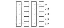
図5Aの配列は、垂直方向の色の繰り返し周期Nが(N=2)であり、図5Bの配列は、(N=4)である。図4は、(N=2)であって、垂直方向の1列のフォトセンサ2、垂直CCD3および垂直CCD3のゲートのバス配線を1列の一部に関して示した模式図である。フォトセンサ2のうちで左上コーナーに斜線部を設けたものが一つの色フィルタ例えばGのフィルタに対応し、斜線部を設けないものが他の色フィルタ、例えばBのフィルタと対応している。垂直CCD3は、上述したように3層電極3相駆動形式のもので、CCDの開口画素(遮光されていない画素)に隣接して3ビットのゲートを有する。また、垂直CCD3は、第1の領域Aと、第2の領域Bを含む。第1の領域Aは、ゲート21、22、23からなり、第2の領域Bは、ゲート31、32、33からなる。ゲート22および32が転送兼読出しゲートである。41、42、42´、43は、垂直転送用の駆動パルスφV1 、φV2 、φV2 ´、φV3 がそれぞれ供給されるバス配線である。
【0019】
ゲート21および31がバス配線41に接続され、ゲート23および33がバス配線43に接続される。これらのバス配線41、43には、それぞれ駆動パルスφV1 、φV3 が供給される。駆動パルスφV2 に関して、2本のバス42および42´が設けられる。第1の領域Aとは、転送兼読出しゲート22がバス42と接続されるものを指し、第2の領域Bは、転送兼読出しゲート32がバス42´と接続されるものを指す。なお、図4では、簡略化のために、バスラインが片側しか描かれていないが、フォトセンサ2の両側にバスラインを配して、両側駆動するのが普通である。
【0020】
この発明では、ライン間引きのために、第1の領域Aがm(m=1,2,3,・・・)並んだ範囲と、第2の領域BがN×a並んだ範囲とが垂直方向に交互に形成される。図4に示す例は、(N=2、m=3、a=2)の場合である。なお、mおよびaの値を任意に選ぶことができるが、mおよびaを大きな値としても、(m+N×a)が有効画素数の垂直画素数より小さいことが必要である。
【0021】
上述したこの発明の一実施例において、第1の動作モード、すなわち、全画素の信号を読出すフルフレームの動作時では、垂直CCD3の第1の領域Aおよび第2の領域Bの両者にフォトセンサ2から信号が読出される。そのためには、バス配線42および42´を通じてゲート22および32の両者に読出しパルスが印加される。この場合、色フィルタの配列の順序と対応する色シーケンス、例えばG、B、G、B、・・・のシーケンスでもって色信号が出力される。
【0022】
一方、第2の動作モード、すなわち、ライン間引き動作時では、第1の領域Aのゲート22にのみバス配線42を介して読出しパルスが印加される。従って、mの範囲から信号が読出され、N×aの範囲からは、信号が読出されない。図4の例では、(m=3)ラインから信号が発生し、(N×a=4)ラインから信号が発生しない。間引かれるライン数が色の繰り返し同期Nの整数倍であるので、ライン間引きの場合の撮像出力の色信号の順序は、フルフレーム読出しと同一の関係に保たれる。
【0023】
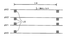
図6A〜図6Cは、撮像素子を駆動する場合のタイミングを示し、図6Aがフルフレームの読出しを行う場合のタイミングを示す。各水平ブランキング期間において、ラインシフトパルスLSとしての3相の駆動パルスφV1 、φV2 、φV2 ´、φV3 が垂直CCD3の第1の領域Aのゲート21、22および23と、第2の領域Bのゲート31、32および33にそれぞれ供給される。また、読出しパルスも1V毎にゲート22および32との両者に対して印加される。この読出しパルスによって、全てのフォトセンサから信号電荷が垂直CCD3に読出される。図6Bの詳細なタイミングチャートに示すように、水平ブランキング期間内で発生する駆動パルスφV1 、φV2 、φV2 ´、φV3 が3相のものであり、1つのラインシフト期間によって1ライン分電荷のシフトがなされる。フルフレームの読出し時には、各水平ブランキング期間内で、1ラインシフトがなされる。
【0024】
一方、ライン間引きの読出しの場合では、図6Cに示すように、第1の領域Aのゲート22にのみ読出しパルスが印加される。それによって、第1の領域Aに隣接したフォトセンサのみから信号電荷が読出される。ライン間引きの場合では、間引かれたラインの垂直CCDには、信号電荷が読出されず、無信号となる。この無信号期間は、ラインシフト動作を複数回繰り返すことによって除去できる。
【0025】
例えば、図4に示す色配列の場合には、H1で示される3画素分の電荷、具体的には、ひとつの第1の領域Aの信号電荷と、2つの第2の領域Bの無信号を、図7に示すように、第1の水平期間H1においてラインシフトパルスLSを3回供給することにより、水平CCD4において合成する。同様に、第2の水平期間H2においてラインシフトパルスLSを3回供給することにより、ひとつの第1の領域Aの信号電荷と、2つの第2の領域Bの無信号を、水平CCD4において合成する。また、第3の水平期間H3において、ラインシフトパルスLSを1回供給することにより、ひとつの第1の領域Aの信号電荷を1水平期間に水平CCD4に供給する。従って、各水平期間において、ひとつの第1の領域からの信号電荷が、色シーケンスが変わることなく出力されることになる。この図7に示す期間の動作が3水平期間毎に繰り返される。
【0026】
図8Aは、(m=1,a=1)の場合の垂直CCD3のチャンネル6のポテンシャルの模式図である。図面に向かって右側から左側の水平CCD4に向かう方向が垂直転送方向である。チャンネル6には、ライン間引き動作時に、信号電荷Qsを含むパケット51と空パケット52とが存在する。各ラインから信号電荷Qsを出力するためには、空パケット52の分、多くラインシフトを行い、それによって信号電荷と無信号とを水平CCD4において混合し、無信号の期間を除去する。各水平ブランキング期間内でなされるラインシフトの回数は、下記の関係を満足するように選定すれば良い。
【0027】
l(:出力する信号電荷Qsを含むパケットの数(この例は1つパケットで考えている))+X(前にある信号電荷Qsを含まないパケットの数)以上で、1+X+(N×a)(:後ろにある信号電荷Qsを含まないパケットの数)以下
それによって、(X=0)の場合では、信号電荷のみを水平CCD4に対して転送し、(X≠0)の場合では、信号電荷を含むパケットと1以上の信号電荷を含まないパケットとを水平CCD4に対して転送する。
【0028】
上述の条件によって、信号電荷を水平CCD4に対して転送し、また、無信号のラインを圧縮することができる。実際には、空パケットの電荷が0ではなく、スミア信号や暗電流等の不要信号電荷Qnが含まれている。各水平ブランキング期間でなされるラインシフトの数が異なると、不要信号電荷Qnの加算される回数が異なるために、不要信号が含まれる量が実際の出力とされるラインによって異なる。それによって、モニタ上のライン毎に輝度が変わって見えるラインクロール現象や、色ずれなどの画質劣化が発生するおそれがある。
【0029】
この問題を解決するには、各水平ブランキング期間でなされるラインシフトの回数を一定とすれば良い。限定された条件、すなわち、(m=1、またはm=2)の場合では、垂直CCD3のラインシフトの数を((N×a/m)+1)とすることによって、各ラインの信号電荷Qsに対して加算される信号電荷Qsを含まないパケットの数を一定とすることができる。これによって、上述した画質劣化の発生を防止することができる。
【0030】
図8Bは、(N=2、m=1、a=1)の場合の垂直CCD3のチャンネル6のポテンシャルの模式図である。この例では、(N×a/m=2)となり、ラインシフトの回数を3回とすることによって、実際の出力となる、各ラインにおいて加算される信号電荷Qsを含まないパケットの数を一定とすることができる。また、図8Cは、(N=2、m=2、a=1)の場合を示す。この場合では、(N×a/m=1)となり、ラインシフトの回数を2回とすれば良い。さらに、m>2の場合でも、スミア信号や暗電流のレベルを充分に小さくすることができれば、問題は生じない。
【0031】
上述したこの発明によるCCDは、実際の出力となるライン数を減少することができるので、垂直CCD3の第1の領域Aの並ぶ数m、第2の領域Bの並ぶ数N×aの値を選ぶことによって、1フィールドのテレビジョンの水平走査線数以下に出力撮像信号のライン数を抑えることができる。ベイヤ方式の色フィルタ配列のような(N=2)の場合を例に出力ライン数のいくつかの例を説明する。
【0032】
図9に示すように、有効画素数(:垂直×水平)が(480×640)のVGA(Video Graphics Array)対応の撮像素子に対してこの発明を適用した場合では、(a=1、m=2)とされる。従って、ライン間引きモードでは、出力ライン数を半分の240ラインとできる。図10に、図9に示す撮像素子の場合の垂直1列の垂直CCDの構造を、図11に図10に示す撮像素子を第2の動作モードで駆動するための駆動パルスのタイミングチャートを示す。尚、図4と対応する部分には、同一の符号を付してその説明を省略する。この場合、各水平期間において、2回ラインシフトパルスLSが供給される。また、第2の動作モードにおいて、第1の水平期間H1には、Rのみの信号が、第2の水平期間H2には、Gのみの信号が読出される。この図10に示す例では、各水平期間に加算されるライン数が同じなので、色ずれの問題などが生じない。
【0033】
図12に示すように、有効画素数が(768×1024)の撮像素子では、(m=1、a=1)とすることによって、出力ライン数を256ラインとできる。図13に、図12に示す撮像素子の場合の垂直1列の垂直CCDの構造を、図14に図13に示す撮像素子を第2の動作モードで駆動するための駆動パルスのタイミングチャートを示す。尚、図4と対応する部分には、同一の符号を付してその説明を省略する。この場合、各水平期間において、3回ラインシフトパルスLSが供給される。また、第2の動作モードにおいて、第1の水平期間H1には、Rのみの信号が、第2の水平期間H2には、Gのみの信号が読出される。また、第1の水平期間H1’に、Rのみの信号を、第2の水平期間H2’に、Gのみの信号を読出すようにしても良い。この図13に示す例では、各水平期間に加算されるライン数が同じなので、色ずれの問題などが生じない。
【0034】
図15に示すように、有効画素数が(1024×1280)の撮像素子では、(m=1、a1 =1、a2 =2)とすることによって、出力ライン数を256ラインとできる。a1 およびa2 は、交互に使用される。図16に、図15に示す撮像素子の場合の垂直1列の垂直CCDの構造を、図17に図16に示す撮像素子を第2の動作モードで駆動するための駆動パルスのタイミングチャートを示す。尚、図4に対応する部分には、同一の符号を付してその説明を省略する。この場合、各水平期間において、4回ラインシフトパルスLSが供給される。また、第2の動作モードにおいて、第1の水平期間H1には、Gのみの信号が、第2の水平期間H2には、Rのみの信号が読出される。また、第1の水平期間H1’に、Rのみの信号を、第2の水平期間H2’に、Gのみの信号を読出すようにしても、第1の水平期間H1”に、Rのみの信号を、第2の水平期間H2”に、Gのみの信号を読出すようにしても良い。この図16に示す例では、各水平期間に加算されるライン数が同じなので、色ずれの問題などが生じない。
【0035】
図9、図12および図15にそれぞれ示す何れの場合でも、出力ライン数を例ばNTSC方式の1フィールドのライン数(262.5)より少なくすることができる。従って、色シーケンスおよび画角をフルフレーム読出しモードと同一の関係を保持して、ライン間引きモードの撮像信号をより短時間で出力することができる。それによって、VRAM、あるいはフレームメモリを使用することなしに、液晶モニタに撮像画面を表示することができる。
【0036】
なお、上述した一実施例における撮像素子の具体的構成は、一例であって、この発明は、これ以外の固体撮像素子に対しても適用できる。例えば垂直CCDが2層電極4相駆動の構造でも良い。さらに、固体撮像素子を駆動するモードとして、読出しパルスφV2 ´を印加し、読出しパルスφV2 を印加しない第3の動作モードを設定するようにしても良い。
【0037】
【発明の効果】
以上説明したように、この発明によれば、全画素を読出すフルフレームの動作モードと、色シーケンスを同一の関係に保って、ライン数の少ない撮像信号を選択的に得ることができ、撮像信号を高速に出力することができる。従って、ライン数の多い撮像素子でも、出力ライン数をテレビジョンの走査線数以下とすることができ、フレームメモリ、VRAM等の大容量メモリを使用しなくても、撮像信号をモニタに表示することができる。また、高速で撮像信号を出力できることにより、オートフォーカス等の自動制御装置の応答を速くすることができる。さらに、コマ数が多くなるので、モニタ画像の動きが滑らかになる利点がある。
【図面の簡単な説明】
【図1】この発明の一実施例の概略的構成を示す略線図である。
【図2】この発明の一実施例の1画素の部分の拡大平面図である。
【図3】この発明の一実施例の垂直CCDの構造を示す略線図である。
【図4】この発明の一実施例の垂直1列のバス配線を示す略線図である。
【図5】この発明を適用することができる色フィルタの一例および他の例を示す略線図である。
【図6】この発明の一実施例を駆動するための駆動パルスのタイミングチャートである。
【図7】図4に示す撮像素子の駆動パルスのタイミングチャートである。
【図8】この発明の一実施例における垂直CCDのポテンシャルを模式的に示す略線図である。
【図9】この発明の具体的な一例を示す略線図である。
【図10】図9に示す撮像素子の垂直1列のバス配線を示す略線図である。
【図11】図9に示す撮像素子の駆動パルスのタイミングチャートである。
【図12】この発明の具体的な他の例を示す略線図である。
【図13】図12に示す撮像素子の垂直1列のバス配線を示す略線図である。
【図14】図12に示す撮像素子の駆動パルスのタイミングチャートである。
【図15】この発明の具体的なさらに他の例を示す略線図である。
【図16】図15に示す撮像素子の垂直1列のバス配線を示す略線図である。
【図17】図15に示す撮像素子の駆動パルスのタイミングチャートである。
【図18】従来の撮像素子の説明に用いる略線図である。
【図19】先に提案されている撮像素子の説明に用いる略線図である。
【図20】撮像素子の出力と液晶モニタの表示との関係を示す略線図である。
【図21】撮像素子から発生した撮像信号を液晶モニタに供給する場合の構成を示すブロック図である。
【符号の説明】
2・・・フォトセンサ、3・・・垂直CCD、4・・・水平CCD、6・・・垂直CCDのチャンネル、8,9,10・・・垂直CCDのゲート、21,22,23・・・垂直CCDの第1の領域Aのゲート、31,32,33・・・垂直CCDの第2の領域Bのゲート、41,42,42´,43・・・駆動パルスを供給するためのバス配線[0001]
BACKGROUND OF THE INVENTION
The present invention is suitable for use in, for example, an electronic still camera for digital recording.Camera system, imaging apparatus, and imaging methodAbout.
[0002]
[Prior art]
Recently, electronic still cameras are becoming popular. A solid-state imaging device suitable for use in an electronic still camera, for example, a CCD having a square lattice and all-pixel readout has been proposed. The square lattice equalizes the vertical interval and the horizontal interval between adjacent pixels, and is used to match the image pickup signal with a personal computer monitor. A CCD used in a conventional video camera or the like accumulates 1/60 second (one field) as shown in FIG. Interlace scanning was realized by reading out the charges, mixing the charges of the two pixels read out by the CCD for vertical transfer, and shifting the combination of the two pixels to be mixed in the up-down direction in the odd and even fields. .
[0003]
Since such a CCD has an accumulation time of 1/60 seconds, it can capture moving images better than a frame accumulation method with an accumulation time of 1/30 seconds, but has the disadvantage of low vertical resolution. is there. Therefore, it is not suitable as an image sensor for an electronic still camera. Therefore, as shown in FIG. 19, an all-pixel reading method has been proposed in which the charges are accumulated for 1/30 seconds and read independently without mixing the charges of all the pixels. According to this method, it is possible to prevent a decrease in vertical resolution, but in order to output an image pickup signal from the image pickup device, when the number of pixels is the same and the readout clock is the same, the above-described video camera This requires twice as much time as the image sensor. More specifically, an imaging signal having a period of 1/30 second is generated.
[0004]
[Problems to be solved by the invention]
In the case of an electronic still camera, a monitor for displaying a captured image, such as a liquid crystal monitor, is often provided in order to focus at the time of shooting or to adjust the camera angle at the time of shooting. A liquid crystal monitor normally displays a television image in a 1/60 second non-interlaced scan. Accordingly, when an image pickup signal having a 1/30 second period is supplied to the liquid crystal monitor as it is, the result becomes as shown in FIG. In order to avoid this, it is necessary to convert the frame rate to the
[0005]
As described above, the image pickup device for reading all pixels is suitable as an image pickup device for an electronic still camera in that it has a high vertical resolution. However, in order to change a frame rate for displaying a picked-up image on a normal television monitor. In addition, a VRAM or a frame memory is required, which increases the cost. Furthermore, since the electronic still camera has automatic control devices such as an automatic focus control device, an automatic iris control device, and an automatic white balance control device, the long period of the output signal of the image sensor is a response to these automatic controls. The problem of slowing down occurred. Furthermore, there has been a problem that the motion of the image displayed on the monitor is not smooth.
[0006]
One method for solving the above problem is to increase the data rate of the output signal of the image sensor. However, when the clock frequency is high, problems such as an increase in power consumption, an increase in the cost of components used, and a deterioration in S / N occur. Therefore, a method for increasing the data rate of the imaging signal is not preferable.
[0007]
Therefore, an object of the present invention is to output an imaging signal at high speed.Camera system, imaging apparatus, and imaging methodIs to provide.
[0008]
[Problems to be solved by the invention]
thisInvention, DroopA plurality of photosensors arranged in a matrix in which light is incident through a plurality of color filters that are repeated in a straight direction with N (N is a natural number) pixel cycles, and charges read from the plurality of photosensors are vertically A vertical transfer unit that transfers the charges from the photosensors connected to the vertical transfer unit without mixing, a horizontal transfer unit that is coupled to the vertical transfer unit and outputs the charges transferred from the vertical transfer unit in one horizontal period cycle, and m (m Is a natural number) of first photosensor groups that are continuous in the vertical direction, and a second photosensor group that is continuous in the vertical direction and has a number a times the pixel period N (a is a natural number). The first photo sensor group and the second photo sensor group are alternately arranged in the vertical direction, and the first photo sensor group is configured to transfer the charge accumulated in the first photo sensor group to the vertical transfer unit. A signal supply unit; And a second signal supply unit for transferring the charges accumulated in the photosensor group to the vertical transfer unit, and the first signal supply unit and the second signal supply unit are provided independently of each other. Solid-state image sensorAnd a drive signal generation unit that generates drive signals that are input to the first and second signal supply units and that drive the vertical transfer unit and the horizontal transfer unit. A camera system that generates a line shift signal as a drive signal for transferring charges from a vertical transfer unit to a horizontal transfer unit during a periodIt is.
[0009]
Further, according to the present invention, charges read from a plurality of photosensors arranged in a matrix in which light is incident through a plurality of color filters that are repeated in a vertical direction with a period of N pixels (N is a natural number) are vertically The transfer unit transfers the charges from the photosensors connected in the vertical direction without mixing, and the charges transferred from the vertical transfer unit are output in one horizontal period cycle by the horizontal transfer unit coupled to the vertical transfer unit. A first photosensor group that is continuous in the vertical direction with m (m is a natural number), and a second photosensor group that is continuous in the vertical direction with a number a times the pixel period N (a is a natural number). The first photo sensor group and the second photo sensor group are arranged alternately in the vertical direction, and the charge accumulated in the first photo sensor group is changed to the first unit. Signal supply unit Steps for transferring to the vertical transfer unit and charges accumulated in the second photosensor group are transferred to the vertical transfer unit by the second signal supply unit provided independently of the first signal supply unit. And a drive signal generation step for generating drive signals that are input to the first and second signal supply units and drive the vertical transfer unit and the horizontal transfer unit. In the drive signal generation step, In the blanking period, a line shift signal is generated as a drive signal for transferring charges from the vertical transfer unit to the horizontal transfer unit.
In addition, the present invention reads from a plurality of photosensors arranged in a matrix form in which light is incident through a plurality of color filters that are repeated in a vertical direction with N (N is a natural number) pixel cycles. Combined with the vertical transfer unit that transfers the charges from the photosensors connected in the vertical direction without mixing, and outputs the charges transferred from the vertical transfer unit as an imaging signal in one horizontal period cycle A horizontal transfer unit that performs m (m is a natural number) first photosensor groups that are continuous in the vertical direction, and a second photosensor that is continuous in the vertical direction that is a times the pixel period N (a is a natural number). The group constitutes one unit, and the first photo sensor group and the second photo sensor group are alternately arranged in the vertical direction, and the charge accumulated in the first photo sensor group is vertically transferred. Forward to department And a second signal supply unit for transferring the charge accumulated in the second photosensor group to the vertical transfer unit. The first signal supply unit and the second signal supply unit The solid-state imaging device in which the signal supply units are provided independently of each other, and the drive signal generation unit that generates drive signals that are input to the first and second signal supply units and drive the vertical transfer unit and the horizontal transfer unit And a display unit that displays the imaging signal, and a storage unit that stores the imaging signal, and the drive signal generation unit stores the first and second signal supply units when storing the imaging signal in the storage unit. When the driving signal is supplied to the display unit and the imaging signal is displayed on the display unit, the driving signal is supplied only to the first signal supply unit.
Further, according to the present invention, charges read from a plurality of photosensors arranged in a matrix in which light is incident through a plurality of color filters that are repeated in a vertical direction with a period of N pixels (N is a natural number) are vertically The transfer unit transfers the charges from the photosensors connected in the vertical direction without mixing, and the charges transferred from the vertical transfer unit are output in one horizontal period cycle by the horizontal transfer unit coupled to the vertical transfer unit. A first photosensor group that is continuous in the vertical direction with m (m is a natural number), and a second photosensor group that is continuous in the vertical direction with a number a times the pixel period N (a is a natural number). The first photo sensor group and the second photo sensor group are arranged alternately in the vertical direction, and the charge accumulated in the first photo sensor group is changed to the first unit. Signal supply unit Steps for transferring to the vertical transfer unit and charges accumulated in the second photosensor group are transferred to the vertical transfer unit by the second signal supply unit provided independently of the first signal supply unit. A step of generating a drive signal that is input to the first and second signal supply units and generates a drive signal for driving the vertical transfer unit and the horizontal transfer unit, and a step of displaying the imaging signal on the display unit. A step of storing the image pickup signal in the storage unit, and the step of generating the drive signal supplies the drive signal to the first and second signal supply units when the image pickup signal is stored in the storage unit. When the signal is displayed on the display unit, the driving signal is supplied only to the first signal supply unit.
[0010]
First and second signal supply units for transfer and reading are provided independently. Accordingly, the first operation mode in which all the pixels are read out through the first and second signal supply units and the second operation mode in which the pixels are read out through one of them can be selectively made possible. In the second operation mode, since the number of lines is thinned out, a high-speed imaging signal can be output. Further, the color arrangement sequence of the imaging signal output in the second operation mode is the same as in the case of all pixel readout, and there is no need to change signal processing. Further, in the second operation mode, when signal charges are transferred from the vertical transfer unit to the horizontal transfer unit, a packet that does not include signal charges is output by performing a predetermined number of line shifts in the horizontal blanking period. Can be compressed so that they are not included.
[0011]
DETAILED DESCRIPTION OF THE INVENTION
Hereinafter, an embodiment of the present invention will be described with reference to the drawings. FIG. 1 schematically shows an embodiment of a
[0012]
A plan view of a unit pixel of the
[0013]
When reading a signal from the
[0014]
The CCD described above is suitable for electronic still cameras and image capture because it can sequentially output all pixel signals without mixing. However, as described above, when charge transfer is performed with the same clock as compared with an image sensor for video cameras having the same number of pixels that performs interlaced output, the output time of one screen (from the upper end to the lower end of the screen) is doubled. It becomes. In one embodiment of the present invention, as a monitor signal, an imaging signal for automatic control such as automatic focus control, the number of horizontal lines is reduced to output an imaging signal for one screen at a high speed. In addition, in the case of this line thinning, the color sequence in the vertical direction defined by the color filter array is not destroyed. On the other hand, when capturing a captured image in a medium such as a semiconductor memory, a full-frame image signal (an image signal in which the number of lines is not thinned) is output. Even in the case of line thinning, since the color sequence is the same as that in the case of a full frame, the problem that the signal processing circuit becomes complicated can be avoided.
[0015]
In the above-described CCD capable of reading all pixels, in order to thin out the number of lines, the wiring for the transfer gate (second polycrystalline silicon) 9 that contributes to reading of the signal charges from the
[0016]
As the arrangement of the color filters of the single-plate CCD, there is an arrangement (Bayer method) in which R (filter that passes red), G (filter that passes green), and B (filter that passes blue) are arranged as shown in FIG. 5A. Are known. A high-sensitivity G filter is arranged in half of the pixels. Further, a complementary color checkered color filter shown in FIG. 5B is also known. In FIG. 5B, Ye, Cy, and Mg are yellow, cyan, and magenta filters, respectively. The complementary color filter shown in FIG. 5B can be improved in resolution as compared with the primary color filter, and is therefore often used in video cameras. On the other hand, the primary color filter shown in FIG. 5A is excellent in terms of color reproducibility, and is often employed in electronic still cameras.
[0017]
The present invention can be applied to both a single-plate image sensor having a primary color filter and a single-plate image sensor having a complementary color filter. Further, although not shown in the drawing, the image pickup device includes an image pickup device having a G filter and an image pickup device having an array of R and B filters, and the positional relationship between the two image pickup devices is a pixel in the horizontal direction or in the horizontal and vertical directions. The present invention can also be applied to an image pickup device (so-called spatial picture element shifting method) shifted by ½ of the pitch.
[0018]
5A, the vertical color repetition period N is (N = 2), and the arrangement in FIG. 5B is (N = 4). FIG. 4 is a schematic diagram showing (N = 2) the photo wirings of one column in the vertical direction, the
[0019]
[0020]
In the present invention, the range in which the first area A is arranged m (m = 1, 2, 3,...) And the area in which the second area B is arranged N × a are perpendicular for line thinning. It is formed alternately in the direction. The example shown in FIG. 4 is a case of (N = 2, m = 3, a = 2). Although the values of m and a can be arbitrarily selected, even if m and a are large values, it is necessary that (m + N × a) is smaller than the number of effective pixels.
[0021]
In the embodiment of the present invention described above, in the first operation mode, that is, in the full frame operation in which the signals of all the pixels are read out, both the first area A and the second area B of the
[0022]
On the other hand, in the second operation mode, that is, in the line thinning operation, the read pulse is applied only to the
[0023]
6A to 6C show timings when driving the image sensor, and FIG. 6A shows timings when full frame reading is performed. In each horizontal blanking period, a three-phase drive pulse φV as a line shift pulse LS1, ΦV2, ΦV2', ΦVThreeAre supplied to the
[0024]
On the other hand, in the case of line thinning readout, a readout pulse is applied only to the
[0025]
For example, in the case of the color arrangement shown in FIG. 4, the charge for three pixels indicated by H1, specifically, the signal charge of one first region A and the no signal of two
[0026]
FIG. 8A is a schematic diagram of the potential of the
[0027]
1 + X + (N × a) equal to or greater than l (: number of packets including signal charge Qs to be output (this example is considered by one packet)) + X (number of packets not including previous signal charge Qs) (: Number of packets that do not include signal charge Qs behind)
Accordingly, in the case of (X = 0), only the signal charge is transferred to the
[0028]
Under the above-described conditions, signal charges can be transferred to the
[0029]
In order to solve this problem, the number of line shifts performed in each horizontal blanking period may be constant. In the case of a limited condition, that is, (m = 1 or m = 2), the number of line shifts of the
[0030]
FIG. 8B is a schematic diagram of the potential of the
[0031]
Since the above-described CCD according to the present invention can reduce the number of lines to be actually output, the values of the number m of the first areas A arranged in the
[0032]
As shown in FIG. 9, when the present invention is applied to a VGA (Video Graphics Array) compatible image sensor having an effective pixel number (: vertical × horizontal) of (480 × 640), (a = 1, m = 2). Therefore, in the line thinning mode, the number of output lines can be reduced to a half of 240 lines. FIG. 10 shows the structure of one vertical CCD in the case of the image sensor shown in FIG. 9, and FIG. 11 shows a timing chart of drive pulses for driving the image sensor shown in FIG. 10 in the second operation mode. . Note that portions corresponding to those in FIG. 4 are denoted by the same reference numerals and description thereof is omitted. In this case, the line shift pulse LS is supplied twice in each horizontal period. In the second operation mode, only the R signal is read in the first horizontal period H1, and only the G signal is read in the second horizontal period H2. In the example shown in FIG. 10, since the number of lines added in each horizontal period is the same, the problem of color misregistration does not occur.
[0033]
As shown in FIG. 12, in an imaging device having an effective pixel number of (768 × 1024), the number of output lines can be set to 256 lines by setting (m = 1, a = 1). FIG. 13 shows the structure of the vertical CCD of one vertical column in the case of the image sensor shown in FIG. 12, and FIG. 14 shows a timing chart of drive pulses for driving the image sensor shown in FIG. 13 in the second operation mode. . Note that portions corresponding to those in FIG. 4 are denoted by the same reference numerals and description thereof is omitted. In this case, three line shift pulses LS are supplied in each horizontal period. In the second operation mode, only the R signal is read in the first horizontal period H1, and only the G signal is read in the second horizontal period H2. Alternatively, only the R signal may be read out during the first horizontal period H1 ', and the G only signal may be read out during the second horizontal period H2'. In the example shown in FIG. 13, since the number of lines added in each horizontal period is the same, the problem of color misregistration does not occur.
[0034]
As shown in FIG. 15, in an image sensor with an effective pixel number of (1024 × 1280), (m = 1, a1= 1, a2= 2), the number of output lines can be 256 lines. a1And a2Are used alternately. FIG. 16 shows a structure of a vertical CCD of one vertical column in the case of the image sensor shown in FIG. 15, and FIG. 17 shows a timing chart of drive pulses for driving the image sensor shown in FIG. 16 in the second operation mode. . Note that portions corresponding to those in FIG. 4 are denoted by the same reference numerals and description thereof is omitted. In this case, the line shift pulse LS is supplied four times in each horizontal period. In the second operation mode, only the G signal is read out during the first horizontal period H1, and only the R signal is read out during the second horizontal period H2. Further, even if the R-only signal is read out in the first horizontal period H1 ′ and the G-only signal is read out in the second horizontal period H2 ′, only the R signal is read out in the first horizontal period H1 ″. It is also possible to read out the signal of only G in the second horizontal period H2 ″. In the example shown in FIG. 16, since the number of lines added in each horizontal period is the same, the problem of color misregistration does not occur.
[0035]
In any of the cases shown in FIGS. 9, 12 and 15, the number of output lines can be made smaller than the number of lines per field (262.5) of the NTSC system, for example. Accordingly, it is possible to output the imaging signal in the line thinning mode in a shorter time while maintaining the same relationship between the color sequence and the angle of view as in the full frame readout mode. Thereby, an imaging screen can be displayed on the liquid crystal monitor without using a VRAM or a frame memory.
[0036]
Note that the specific configuration of the image sensor in the above-described embodiment is an example, and the present invention can be applied to other solid-state image sensors. For example, the vertical CCD may have a two-layer electrode four-phase drive structure. Further, as a mode for driving the solid-state imaging device, the readout pulse φV2'And read pulse φV2A third operation mode in which no voltage is applied may be set.
[0037]
【The invention's effect】
As described above, according to the present invention, it is possible to selectively obtain an imaging signal with a small number of lines while maintaining the same relationship between the full-frame operation mode for reading all pixels and the color sequence. Signals can be output at high speed. Therefore, even in an image sensor with a large number of lines, the number of output lines can be made equal to or less than the number of scanning lines of a television, and an image signal is displayed on a monitor without using a large capacity memory such as a frame memory or a VRAM. be able to. Further, since the imaging signal can be output at a high speed, the response of an automatic control device such as autofocus can be accelerated. Furthermore, since the number of frames increases, there is an advantage that the monitor image moves smoothly.
[Brief description of the drawings]
FIG. 1 is a schematic diagram showing a schematic configuration of an embodiment of the present invention.
FIG. 2 is an enlarged plan view of a portion of one pixel according to an embodiment of the present invention.
FIG. 3 is a schematic diagram showing the structure of a vertical CCD according to an embodiment of the present invention.
FIG. 4 is a schematic diagram showing one line of bus wiring in one embodiment of the present invention.
FIG. 5 is a schematic diagram illustrating an example of a color filter to which the present invention can be applied and another example.
FIG. 6 is a timing chart of drive pulses for driving one embodiment of the present invention.
7 is a timing chart of drive pulses of the image sensor shown in FIG.
FIG. 8 is a schematic diagram schematically showing the potential of a vertical CCD in one embodiment of the present invention.
FIG. 9 is a schematic diagram showing a specific example of the present invention.
10 is a schematic diagram showing bus lines in one vertical row of the image sensor shown in FIG. 9;
11 is a timing chart of drive pulses of the image sensor shown in FIG. 9. FIG.
FIG. 12 is a schematic diagram showing another specific example of the present invention.
13 is a schematic diagram showing bus lines in one vertical column of the image sensor shown in FIG. 12. FIG.
14 is a timing chart of drive pulses of the image sensor shown in FIG.
FIG. 15 is a schematic diagram showing still another specific example of the present invention.
16 is a schematic diagram showing bus lines in one vertical column of the image sensor shown in FIG. 15;
17 is a timing chart of drive pulses of the image sensor shown in FIG.
FIG. 18 is a schematic diagram used to describe a conventional image sensor.
FIG. 19 is a schematic diagram used for explanation of the previously proposed image sensor;
FIG. 20 is a schematic diagram illustrating a relationship between an output of an image sensor and a display on a liquid crystal monitor.
FIG. 21 is a block diagram illustrating a configuration when an imaging signal generated from an imaging element is supplied to a liquid crystal monitor.
[Explanation of symbols]
2 ... photo sensor, 3 ... vertical CCD, 4 ... horizontal CCD, 6 ... channel of vertical CCD, 8,9,10 ... gate of vertical CCD, 21,22,23 ... -Gate of the first area A of the vertical CCD, 31, 32, 33 ... Gate of the second area B of the vertical CCD, 41, 42, 42 ', 43 ... Bus for supplying drive pulses wiring
Claims (13)
上記第1および第2の信号供給部に入力され、上記垂直転送部および上記水平転送部を駆動する駆動信号を生成する駆動信号生成部と
を有するカメラシステムにおいて、
上記駆動信号生成部は、水平ブランキング期間に、上記垂直転送部から上記水平転送部へ上記電荷を転送するための上記駆動信号としてラインシフト信号を生成することを特徴とするカメラシステム。A plurality of photosensors arranged in a matrix in which light is incident through a plurality of color filters that are repeated in a vertical direction at a period of N (N is a natural number) pixels, and charges read from the plurality of photosensors are vertically A vertical transfer unit that transfers charges from the photosensors connected in the direction without mixing, a horizontal transfer unit that is coupled to the vertical transfer unit and outputs the charges transferred from the vertical transfer unit in one horizontal period cycle; m (m is a natural number) first photo sensor groups that are continuous in the vertical direction, and a second photo sensor group that is continuous in the vertical direction that is a number (a is a natural number) times the pixel period N. The first photo sensor group and the second photo sensor group are arranged alternately in the vertical direction, and charge accumulated in the first photo sensor group is transferred to the vertical transfer unit. Forward to And a first signal supply unit for transferring charges accumulated in the second photosensor group to the vertical transfer unit, and the first signal supply unit. And a solid-state imaging device in which the second signal supply unit is provided independently of each other;
In a camera system including a drive signal generation unit that generates a drive signal that is input to the first and second signal supply units and drives the vertical transfer unit and the horizontal transfer unit.
The camera system, wherein the drive signal generation unit generates a line shift signal as the drive signal for transferring the charge from the vertical transfer unit to the horizontal transfer unit in a horizontal blanking period.
上記駆動信号生成部は、
上記第1および第2の信号供給部に駆動信号を供給することで全画素の電荷を読出す第1の動作モードと、
上記第1の信号供給部のみを駆動する駆動信号を生成する第2の動作モードとを選択的に切り換え可能であることを特徴とするカメラシステム。The camera system of claim 1.
The drive signal generator is
A first operation mode for reading out charges of all pixels by supplying drive signals to the first and second signal supply units;
A camera system capable of selectively switching between a second operation mode for generating a drive signal for driving only the first signal supply unit.
上記駆動信号生成部は、連続するm個の水平ブランキング期間における各水平ブランキング期間で、m個の上記第1のフォトセンサ群の1画素から読み出された電荷を上記水平転送部へ転送するためのラインシフト信号を含む1以上のラインシフト信号を生成し、連続するm個の水平ブランキング期間全体で(m+N×a)回上記ラインシフト信号を生成することを特徴とするカメラシステム。The camera system of claim 1.
The drive signal generating unit is communicating with the m horizontal blanking Contact Keru each horizontal blanking period during which connection to, the horizontal transfer charges read from the m above one pixel of the first photo sensor group One or more line shift signals including a line shift signal to be transferred to a part are generated, and the line shift signal is generated (m + N × a) times in the entire m horizontal blanking periods. Camera system.
上記駆動信号生成部は、或る第1のフォトセンサ群に含まれる1つの画素を第1の画素とした際に、
上記或る第1のフォトセンサ群に含まれ、上または下方向において上記第1の画素に隣接する第2の画素の電荷と、上記第1の画素の電荷とをそれぞれ異なる水平ブランキング期間に上記垂直転送部から上記水平転送部に転送させるように、ラインシフト信号を生成することを特徴とするカメラシステム。The camera system of claim 1.
When the drive signal generation unit sets one pixel included in a certain first photosensor group as the first pixel,
The charge of the second pixel that is included in the first photosensor group and is adjacent to the first pixel in the upward or downward direction and the charge of the first pixel are in different horizontal blanking periods. A camera system, wherein a line shift signal is generated so as to be transferred from the vertical transfer unit to the horizontal transfer unit.
上記駆動信号生成部は、上記mが2である場合に、
上記或る第1のフォトセンサ群に含まれ、上方向において上記第1の画素に隣接する画素を上記第2の画素、下方向において上記第1の画素と隣接する画素を第3の画素とした際に、
上記第2および第3の画素のうち上記第1の画素との物理的距離が長い方の画素と、上記第1の画素との間に位置する画素の電荷を、上記物理的距離が長い方の画素の電荷と加算されるようにするため、上記物理的距離が長い方の画素の電荷を上記垂直転送部から上記水平転送部に転送する水平ブランキング期間に、少なくとも2つのラインシフト信号を生成することを特徴とするカメラシステム。The camera system according to claim 4.
When the m is 2 , the drive signal generation unit
A pixel included in the first photosensor group, the pixel adjacent to the first pixel in the upward direction is the second pixel, and the pixel adjacent to the first pixel in the downward direction is the third pixel. When
And picture elements of the physical distance longer between the second and third pixel sac Chi upper Symbol first pixel, the charge of the pixels located between the first pixel, the upper Symbol physical In order to be added to the charge of the pixel having the longer distance, at least two in the horizontal blanking period in which the charge of the pixel having the longer physical distance is transferred from the vertical transfer unit to the horizontal transfer unit. A camera system for generating a line shift signal.
上記駆動信号生成部は、各水平期間において、同一数のラインシフト信号を生成することを特徴とするカメラシステム。The camera system of claim 1.
The drive signal generation unit generates the same number of line shift signals in each horizontal period.
上記aが各単位で異なることを特徴とするカメラシステム。The camera system of claim 1.
A camera system characterized in that a is different for each unit.
上記aが2単位周期であり、各単位毎に1、2の順であることを特徴とするカメラシステム。The camera system of claim 1.
2. The camera system according to claim 1 , wherein a is a unit cycle and is in the order of 1 and 2 for each unit.
上記Nがどの単位においても2で固定であることを特徴とするカメラシステム。The camera system of claim 1.
A camera system wherein N is fixed at 2 in any unit.
m=1またはm=2の場合において、
上記駆動信号生成部は、各水平ブランキング期間に(N×a/m)+1個のラインシフト信号を生成し、
これにより、信号電荷を含む1ラインの画素の電荷と、信号電荷を含まないN×a/mラインの画素の電荷とが上記水平転送部において混合されることを特徴とするカメラシステム。The camera system of claim 1.
In the case of m = 1 or m = 2,
The drive signal generator generates (N × a / m) +1 line shift signals in each horizontal blanking period,
Thereby, the charge of one line of pixels including signal charges and the charge of pixels of N × a / m lines not including signal charges are mixed in the horizontal transfer unit.
上記垂直転送部から転送された電荷を、上記垂直転送部と結合される水平転送部により1水平期間周期で出力するステップと、
m(mは自然数)個の垂直方向に連なる第1のフォトセンサ群と、上記画素周期Nのa倍(aは自然数)の数からなる垂直方向に連なる第2のフォトセンサ群とで、1単位を構成し、上記第1のフォトセンサ群と、上記第2のフォトンサ群とが垂直方向に交互に配置されるものとし、上記第1のフォトセンサ群に蓄積された電荷を、第1の信号供給部により上記垂直転送部に転送させるためのステップと、
上記第2のフォトセンサ群に蓄積された電荷を、上記第1の信号供給部と互いに独立して設けられる第2の信号供給部により上記垂直転送部に転送させるステップと、
上記第1および第2の信号供給部に入力され、上記垂直転送部および上記水平転送部を駆動する駆動信号を生成する駆動信号生成のステップと
を有し、
上記駆動信号生成のステップでは、水平ブランキング期間に、上記垂直転送部から上記水平転送部へ上記電荷を転送するための上記駆動信号としてラインシフト信号を生成することを特徴とする撮像方法。Charges read from a plurality of photosensors arranged in a matrix in which light is incident through a plurality of color filters that are repeated in a vertical direction with N (N is a natural number) pixel cycles are vertically transferred by a vertical transfer unit. Transferring the charge from the photosensors connected to without mixing,
Outputting the charges transferred from the vertical transfer unit in one horizontal period cycle by a horizontal transfer unit coupled to the vertical transfer unit;
m (m is a natural number) first photo sensor groups that are continuous in the vertical direction, and a second photo sensor group that is continuous in the vertical direction that is a number (a is a natural number) times the pixel period N. The unit is configured such that the first photosensor group and the second photosensor group are alternately arranged in the vertical direction, and the electric charge accumulated in the first photosensor group is A step for causing the signal supply unit to transfer to the vertical transfer unit;
Transferring the charge accumulated in the second photosensor group to the vertical transfer unit by a second signal supply unit provided independently of the first signal supply unit;
A drive signal generation step for generating a drive signal that is input to the first and second signal supply units and drives the vertical transfer unit and the horizontal transfer unit;
In the driving signal generation step, a line shift signal is generated as the driving signal for transferring the charge from the vertical transfer unit to the horizontal transfer unit in a horizontal blanking period.
上記第1の信号供給部と上記第2の信号供給部が互いに独立して設けられている固体撮像素子と、
上記第1および第2の信号供給部に入力され、上記垂直転送部および上記水平転送部を駆動する駆動信号を生成する駆動信号生成部と、
上記撮像信号を表示する表示部と、
上記撮像信号を記憶する記憶部と
を有し、
上記駆動信号生成部は、上記撮像信号を上記記憶部に記憶する際には、上記第1および第2の信号供給部に駆動信号を供給し、上記撮像信号を上記表示部に表示する際には、上記第1の信号供給部のみに駆動信号を供給することを特徴とする撮像装置。A plurality of photosensors arranged in a matrix in which light is incident through a plurality of color filters that are repeated in a vertical direction at a period of N (N is a natural number) pixels, and charges read from the plurality of photosensors are vertically A vertical transfer unit that transfers charges from photosensors connected in the direction without mixing, and a horizontal transfer that is coupled to the vertical transfer unit and outputs the charges transferred from the vertical transfer unit as an imaging signal in one horizontal period cycle A first photosensor group that continues in the vertical direction, and a second photosensor group that continues in the vertical direction, which is a number (a is a natural number) times the pixel period N. The first photo sensor group and the second photo sensor group are alternately arranged in the vertical direction, and charge accumulated in the first photo sensor group is Drooping A first signal supplying unit for transferring the transfer portion, becomes the electric charge accumulated in the second photosensor groups and a second signal supplying unit for transferring to the vertical transfer section,
A solid-state imaging device in which the first signal supply unit and the second signal supply unit are provided independently of each other;
A drive signal generator that is input to the first and second signal supply units and generates a drive signal for driving the vertical transfer unit and the horizontal transfer unit;
A display unit for displaying the imaging signal;
A storage unit for storing the imaging signal,
The drive signal generation unit supplies the drive signal to the first and second signal supply units when storing the image pickup signal in the storage unit, and displays the image pickup signal on the display unit. The image pickup apparatus supplies a drive signal only to the first signal supply unit.
上記垂直転送部から転送された電荷を、上記垂直転送部と結合される水平転送部により1水平期間周期で出力するステップと、
m(mは自然数)個の垂直方向に連なる第1のフォトセンサ群と、上記画素周期Nのa倍(aは自然数)の数からなる垂直方向に連なる第2のフォトセンサ群とで、1単位を構成し、上記第1のフォトセンサ群と、上記第2のフォトンサ群とが垂直方向に交互に配置されるものとし、上記第1のフォトセンサ群に蓄積された電荷を、第1の信号供給部により上記垂直転送部に転送させるためのステップと、
上記第2のフォトセンサ群に蓄積された電荷を、上記第1の信号供給部と互いに独立して設けられる第2の信号供給部により上記垂直転送部に転送させるステップと、
上記第1および第2の信号供給部に入力され、上記垂直転送部および上記水平転送部を駆動する駆動信号を生成する駆動信号生成のステップと、
上記撮像信号を表示部に表示するステップと、
上記撮像信号を記憶部に記憶するステップと
を有し、
上記駆動信号生成のステップは、上記撮像信号を上記記憶部に記憶する際には、上記第1および第2の信号供給部に駆動信号を供給し、上記撮像信号を上記表示部により表示する際には、上記第1の信号供給部のみに駆動信号を供給することを特徴とする撮像方法。Charges read from a plurality of photosensors arranged in a matrix in which light is incident through a plurality of color filters that are repeated in a vertical direction with N (N is a natural number) pixel cycles are vertically transferred by a vertical transfer unit. Transferring the charge from the photosensors connected to without mixing,
Outputting the charges transferred from the vertical transfer unit in one horizontal period cycle by a horizontal transfer unit coupled to the vertical transfer unit;
m (m is a natural number) first photo sensor groups that are continuous in the vertical direction, and a second photo sensor group that is continuous in the vertical direction that is a number (a is a natural number) times the pixel period N. The unit is configured such that the first photosensor group and the second photosensor group are alternately arranged in the vertical direction, and the electric charge accumulated in the first photosensor group is A step for causing the signal supply unit to transfer to the vertical transfer unit;
Transferring the charge accumulated in the second photosensor group to the vertical transfer unit by a second signal supply unit provided independently of the first signal supply unit;
A drive signal generation step of generating drive signals that are input to the first and second signal supply units and drive the vertical transfer unit and the horizontal transfer unit;
Displaying the imaging signal on a display unit;
Storing the imaging signal in a storage unit,
In the drive signal generation step, when the image pickup signal is stored in the storage unit, the drive signal is supplied to the first and second signal supply units, and the image pickup signal is displayed on the display unit. In the imaging method, the drive signal is supplied only to the first signal supply unit.
Priority Applications (3)
| Application Number | Priority Date | Filing Date | Title |
|---|---|---|---|
| JP03017997A JP3948042B2 (en) | 1996-03-06 | 1997-02-14 | Camera system, imaging apparatus, and imaging method |
| US08/807,201 US20020057349A1 (en) | 1996-03-06 | 1997-02-28 | Image pickup apparatus and solid state image pickup device |
| US09/193,391 US6342921B1 (en) | 1996-03-06 | 1998-11-18 | Lattice-type solid state image pickup device |
Applications Claiming Priority (3)
| Application Number | Priority Date | Filing Date | Title |
|---|---|---|---|
| JP7831596 | 1996-03-06 | ||
| JP8-78315 | 1996-03-06 | ||
| JP03017997A JP3948042B2 (en) | 1996-03-06 | 1997-02-14 | Camera system, imaging apparatus, and imaging method |
Publications (2)
| Publication Number | Publication Date |
|---|---|
| JPH09298755A JPH09298755A (en) | 1997-11-18 |
| JP3948042B2 true JP3948042B2 (en) | 2007-07-25 |
Family
ID=26368481
Family Applications (1)
| Application Number | Title | Priority Date | Filing Date |
|---|---|---|---|
| JP03017997A Expired - Lifetime JP3948042B2 (en) | 1996-03-06 | 1997-02-14 | Camera system, imaging apparatus, and imaging method |
Country Status (1)
| Country | Link |
|---|---|
| JP (1) | JP3948042B2 (en) |
Families Citing this family (5)
| Publication number | Priority date | Publication date | Assignee | Title |
|---|---|---|---|---|
| JP3469801B2 (en) | 1999-02-02 | 2003-11-25 | オリンパス光学工業株式会社 | Solid-state imaging device |
| KR100412995B1 (en) * | 2002-03-29 | 2003-12-31 | 주식회사 하이닉스반도체 | Image sensor having parallel analog bus lines and column drive circuit |
| JP2007295230A (en) | 2006-04-25 | 2007-11-08 | Matsushita Electric Ind Co Ltd | Solid state imaging apparatus, driving method thereof, and camera |
| JP2008035279A (en) * | 2006-07-28 | 2008-02-14 | Sanyo Electric Co Ltd | Pixel information reading method and imaging apparatus |
| JP4688766B2 (en) | 2006-09-21 | 2011-05-25 | パナソニック株式会社 | Solid-state imaging device, driving method thereof and camera |
-
1997
- 1997-02-14 JP JP03017997A patent/JP3948042B2/en not_active Expired - Lifetime
Also Published As
| Publication number | Publication date |
|---|---|
| JPH09298755A (en) | 1997-11-18 |
Similar Documents
| Publication | Publication Date | Title |
|---|---|---|
| US10554917B2 (en) | Electric camera | |
| JP3511772B2 (en) | Solid-state imaging device, driving method of solid-state imaging device, camera device and camera system | |
| US4831453A (en) | Solid-state imaging device having high-speed shutter function and method of realizing high-speed function in solid-state imaging device | |
| KR100606379B1 (en) | Solid-state image pickup element and camera having the same | |
| JP3800673B2 (en) | Solid-state imaging device and driving method thereof | |
| JP2003052049A (en) | Imaging apparatus | |
| KR100317570B1 (en) | Method of driving solid-state image sensor | |
| JP2007295230A (en) | Solid state imaging apparatus, driving method thereof, and camera | |
| JP3854662B2 (en) | Imaging device | |
| KR100448302B1 (en) | Solid state image pickup device of an interline system | |
| US7701498B2 (en) | Solid-state image pickup device, drive method therefor and camera | |
| JP2011077939A (en) | Solid-state imaging device and camera with the same | |
| JP3948042B2 (en) | Camera system, imaging apparatus, and imaging method | |
| JP3459738B2 (en) | Imaging device | |
| JP3985275B2 (en) | Imaging apparatus and imaging method | |
| JP3948456B2 (en) | Solid-state image sensor and control method of solid-state image sensor | |
| JP4227203B2 (en) | Imaging device | |
| JP2005191943A (en) | Solid-state imaging device and camera equipped with the same | |
| JP2000115643A (en) | Drive method for solid-state image pickup device, the solid-state image pickup device, solid-state image pickup element and image pickup camera | |
| JP2001145025A (en) | Solid-state image pickup device and its drive method | |
| JP4311473B2 (en) | Imaging device | |
| JP3392607B2 (en) | Driving method of solid-state imaging device | |
| JPH10336510A (en) | Solid-state image-pickup device | |
| JP4347981B2 (en) | Driving method of solid-state imaging device | |
| JP3878775B2 (en) | Solid-state imaging device, camera using the same, and driving method of solid-state imaging device |
Legal Events
| Date | Code | Title | Description |
|---|---|---|---|
| A977 | Report on retrieval |
Free format text: JAPANESE INTERMEDIATE CODE: A971007 Effective date: 20060214 |
|
| A131 | Notification of reasons for refusal |
Free format text: JAPANESE INTERMEDIATE CODE: A131 Effective date: 20060307 |
|
| A521 | Request for written amendment filed |
Free format text: JAPANESE INTERMEDIATE CODE: A523 Effective date: 20060508 |
|
| TRDD | Decision of grant or rejection written | ||
| A01 | Written decision to grant a patent or to grant a registration (utility model) |
Free format text: JAPANESE INTERMEDIATE CODE: A01 Effective date: 20070327 |
|
| A61 | First payment of annual fees (during grant procedure) |
Free format text: JAPANESE INTERMEDIATE CODE: A61 Effective date: 20070409 |
|
| FPAY | Renewal fee payment (event date is renewal date of database) |
Free format text: PAYMENT UNTIL: 20100427 Year of fee payment: 3 |
|
| FPAY | Renewal fee payment (event date is renewal date of database) |
Free format text: PAYMENT UNTIL: 20110427 Year of fee payment: 4 |
|
| FPAY | Renewal fee payment (event date is renewal date of database) |
Free format text: PAYMENT UNTIL: 20120427 Year of fee payment: 5 |
|
| FPAY | Renewal fee payment (event date is renewal date of database) |
Free format text: PAYMENT UNTIL: 20130427 Year of fee payment: 6 |
|
| FPAY | Renewal fee payment (event date is renewal date of database) |
Free format text: PAYMENT UNTIL: 20140427 Year of fee payment: 7 |
|
| R250 | Receipt of annual fees |
Free format text: JAPANESE INTERMEDIATE CODE: R250 |
|
| R250 | Receipt of annual fees |
Free format text: JAPANESE INTERMEDIATE CODE: R250 |
|
| R250 | Receipt of annual fees |
Free format text: JAPANESE INTERMEDIATE CODE: R250 |
|
| EXPY | Cancellation because of completion of term |