JP3943273B2 - Solid-state imaging device and signal readout method - Google Patents
Solid-state imaging device and signal readout method Download PDFInfo
- Publication number
- JP3943273B2 JP3943273B2 JP02002899A JP2002899A JP3943273B2 JP 3943273 B2 JP3943273 B2 JP 3943273B2 JP 02002899 A JP02002899 A JP 02002899A JP 2002899 A JP2002899 A JP 2002899A JP 3943273 B2 JP3943273 B2 JP 3943273B2
- Authority
- JP
- Japan
- Prior art keywords
- signal
- color
- supplied
- mode
- transfer
- Prior art date
- Legal status (The legal status is an assumption and is not a legal conclusion. Google has not performed a legal analysis and makes no representation as to the accuracy of the status listed.)
- Expired - Fee Related
Links
Images


Classifications
-
- H—ELECTRICITY
- H04—ELECTRIC COMMUNICATION TECHNIQUE
- H04N—PICTORIAL COMMUNICATION, e.g. TELEVISION
- H04N23/00—Cameras or camera modules comprising electronic image sensors; Control thereof
- H04N23/60—Control of cameras or camera modules
- H04N23/667—Camera operation mode switching, e.g. between still and video, sport and normal or high- and low-resolution modes
-
- H—ELECTRICITY
- H04—ELECTRIC COMMUNICATION TECHNIQUE
- H04N—PICTORIAL COMMUNICATION, e.g. TELEVISION
- H04N23/00—Cameras or camera modules comprising electronic image sensors; Control thereof
- H04N23/70—Circuitry for compensating brightness variation in the scene
- H04N23/71—Circuitry for evaluating the brightness variation
-
- H—ELECTRICITY
- H04—ELECTRIC COMMUNICATION TECHNIQUE
- H04N—PICTORIAL COMMUNICATION, e.g. TELEVISION
- H04N25/00—Circuitry of solid-state image sensors [SSIS]; Control thereof
- H04N25/10—Circuitry of solid-state image sensors [SSIS]; Control thereof for transforming different wavelengths into image signals
- H04N25/11—Arrangement of colour filter arrays [CFA]; Filter mosaics
- H04N25/13—Arrangement of colour filter arrays [CFA]; Filter mosaics characterised by the spectral characteristics of the filter elements
- H04N25/134—Arrangement of colour filter arrays [CFA]; Filter mosaics characterised by the spectral characteristics of the filter elements based on three different wavelength filter elements
-
- H—ELECTRICITY
- H04—ELECTRIC COMMUNICATION TECHNIQUE
- H04N—PICTORIAL COMMUNICATION, e.g. TELEVISION
- H04N25/00—Circuitry of solid-state image sensors [SSIS]; Control thereof
- H04N25/40—Extracting pixel data from image sensors by controlling scanning circuits, e.g. by modifying the number of pixels sampled or to be sampled
- H04N25/42—Extracting pixel data from image sensors by controlling scanning circuits, e.g. by modifying the number of pixels sampled or to be sampled by switching between different modes of operation using different resolutions or aspect ratios, e.g. switching between interlaced and non-interlaced mode
-
- H—ELECTRICITY
- H04—ELECTRIC COMMUNICATION TECHNIQUE
- H04N—PICTORIAL COMMUNICATION, e.g. TELEVISION
- H04N25/00—Circuitry of solid-state image sensors [SSIS]; Control thereof
- H04N25/40—Extracting pixel data from image sensors by controlling scanning circuits, e.g. by modifying the number of pixels sampled or to be sampled
- H04N25/44—Extracting pixel data from image sensors by controlling scanning circuits, e.g. by modifying the number of pixels sampled or to be sampled by partially reading an SSIS array
- H04N25/445—Extracting pixel data from image sensors by controlling scanning circuits, e.g. by modifying the number of pixels sampled or to be sampled by partially reading an SSIS array by skipping some contiguous pixels within the read portion of the array
-
- H—ELECTRICITY
- H04—ELECTRIC COMMUNICATION TECHNIQUE
- H04N—PICTORIAL COMMUNICATION, e.g. TELEVISION
- H04N25/00—Circuitry of solid-state image sensors [SSIS]; Control thereof
- H04N25/70—SSIS architectures; Circuits associated therewith
- H04N25/71—Charge-coupled device [CCD] sensors; Charge-transfer registers specially adapted for CCD sensors
- H04N25/73—Charge-coupled device [CCD] sensors; Charge-transfer registers specially adapted for CCD sensors using interline transfer [IT]
Description
【0001】
【発明の属する技術分野】
本発明は、入射光を電気信号に変換して被写界の像を装置に取り込む固体撮像装置および信号読出し方法に関し、特に、解像度の向上を図るため、高集積化させるとともに、斜めに隣接する撮像デバイス、すなわち、画素を互いにその画素中心に対して1/2 ピッチずつずらして配する、いわゆる、ハニカム型に画素配置された電子スチルカメラ装置や画像入力装置等に用いて好適なものである。
【0002】
【従来の技術】
高集積化により解像度を向上させる観点から、最近、新たな受光素子の配置として、受光素子の幾何学的な形状の中心を行方向および列方向にピッチの半分ずらして配置する、いわゆるハニカム配置の固体撮像装置に対して、特公平4-31231 号公報、特開平6-77450 号公報および特開平10-136391 号公報等のように様々な提案がされている。特公平4-31231 号公報において、いわゆる、画素ずらし配置されている光センス手段に沿って第1の電極を波状パターンに蛇行させ、この波状パターンと反対位相のパターンに第2の電極を形成し、第1の電極と第2の電極が互いに離散する領域に他の光センス手段を配置して、第1の電極に与えられる活性化信号に応答して第2の電極と選択的に結合する手段を介して光センス手段から信号を読み出すことにより、解像度および感度を従来よりも向上させている。ここで、光センサ手段は、形状を八角形に形成された場合が例示されている。
【0003】
特開平6-77450 号公報では、受光素子の形状を菱形の一つである正方形にして各辺が垂直方向に45°の角度をなすようにして開口率を高くして固体撮像装置の小型化が図られている。特にハニカム配置を採用することで垂直解像度の向上を図っている。また、各受光素子の上にはマイクロレンズを配設して集光効率を向上させている。
【0004】
また、特開平10-136391 号公報では、隣接する行の光電変換素子の配列間隔のほぼ1/2 だけ相対的にずらし同一行の隣接する光電変換素子間に2列分の列方向で電荷転送装置が配され、その一つが斜め方向に隣接する光電変換素子からの電荷転送に用いてする電荷転送装置を蛇行させて形成することにより、光電変換素子の高集積化、受光光率の向上等を図りながら、モアレ等の偽信号の抑制が行われている。前述した特公平4-31231 号公報および特開平6-77450 号公報では、高集積化を行う上でのデバイスの構造だけに着目されているに過ぎない。また、特開平10-136391 号公報では、デバイスの構造およびデバイスの形状や色フィルタの配置関係が述べられている。そして、これらの関係を用いた全画素読出しについての記載がされている。
【0005】
【発明が解決しようとする課題】
ところで、このような高集積化に伴って光電変換により得られた信号電荷の読出しに時間を要してしまうことが懸念される。たとえば、オートフォーカス調整(AF:Automatic Focus)や自動露出制御(AE:Automatic Exposure )を行うような測光制御モードでは、信号電荷の読出しの所要時間を短くし、撮像の準備を早急に完了させたいという要求がある。撮像デバイスにとって撮像素子の高集積化と信号読出しの短縮化は、互いに相反する、二律背反的な要求である。特に、ハニカム配置の撮像デバイスから測光制御モードで高速に信号読出しする場合、これまでと異なる方法によるブレイクスルーが必要になる。
【0006】
本発明はこのような従来技術の欠点を解消し、撮像素子を高集積化させても、たとえば、測光制御のような場合信号読出しを短縮化させることのできる固体撮像装置および信号読出し方法を提供することを目的とする。
【0007】
【課題を解決するための手段】
本発明は上述の課題を解決するために、入射光が集光する集光面に該入射光を光電変換する複数の受光素子を2次元的に配され、この複数の受光素子のそれぞれのうちで斜めに隣接する素子は、ピッチを行方向および列方向に1/2 ずつずらした相互の位置関係に配され、この複数の受光素子のそれぞれでの光電変換により得られた信号電荷をそれぞれの所定のタイミングで駆動信号に応動して転送する撮像手段から出力される撮像信号をディジタル信号に変換し、この信号に信号処理を施して画像信号を生成する固体撮像装置において、撮像手段に、入射光を三原色RGB にそれぞれ色分解する色フィルタのうち、少なくとも色フィルタG が列方向に配された色分解手段と、複数の受光素子のそれぞれに対応して配される列方向の転送素子にだけ信号電荷を飛越し転送させる信号読出し手段とを含み、この装置に撮像手段からの信号電荷の読出し動作を表すモードのうち、複数の撮像素子すべてから信号電荷を読み出す全画素読出しモードおよび色G だけを読み出す指定読出しモードのいずれか一方のモードを指定するモード指定手段と、このモード指定手段の指示に応じて駆動信号を生成するとともに、モードに応じて生成した駆動信号の供給先を選択して供給する駆動信号生成手段と、モード指定手段からの指示を受けて駆動信号生成手段に対してモード毎の駆動信号の生成を制御するとともに、撮像信号に施される信号処理も制御する制御手段とを含むことを特徴とする。
【0008】
ここで、色分解手段は、色フィルタの中で、色G を列方向にストライプ状に配するとともに、色G が正方格子状に配され、この色G を挟んで対角位置に同色R,またはB が配される完全市松または色G 正方格子状に配され、色G を挟んで対角位置に異色R, B、かつ同一行に同色の色フィルタが配される市松パターンを用いることが好ましい。これにより、色G だけを取り出す場合、色の混合を避けることができる。
【0009】
駆動信号生成手段は、指定読出しモードの場合に色フィルタの色G に対応する受光素子に隣接した信号読出し手段だけに駆動信号を選択的に供給することが好ましい。
【0010】
また、駆動信号生成手段は、指定読出しモードの場合に、さらに選択的に前記駆動信号が供給される信号読出し手段のうち、画像を構成する有効画面の、列方向の中央からほぼ対称に、少なくとも1/4 以上の所定の領域の前記信号読出し手段だけに独立した指定駆動信号を供給することが望ましい。これにより、信号電荷の読出し領域を狭く指定できるので、一層信号電荷の読出しに要する時間を領域の大きさに応じて少なく済ませることができる。
【0011】
撮像手段は、列方向に配する複数の転送素子を8個単位にし、各転送素子に対応させて所定のタイミングの駆動信号が供給される電極のうち、色G の色フィルタの受光素子に隣接する2つの電極だけにフィールドシフトを行う信号読出し手段が配設され、所定の領域に配される2つの電極に対応する指定電極には、全画素読出しモードで供給される駆動信号とは独立な配線で指定駆動信号が供給されることが好ましい。
【0012】
そして、信号読出し手段は、8個単位の転送素子のうち、色G では第1および第5の転送素子に、色R, Bの両方を含む列では、第3および第7の転送素子に配設することよい。
【0013】
本発明の固体撮像装置は、モード指定手段でモードを設定し、この指定したモードの信号を制御手段に供給する。この供給により制御手段は、駆動信号生成手段を制御して駆動信号を生成する。撮像手段には、色フィルタG が列方向に配された色分解手段を介して入射光が供給される。撮像手段は、この入射光を各受光素子で光電変換し、指定のモードに応じて駆動信号生成手段から供給される駆動信号を信号読出し手段に供給し、信号電荷の飛越し転送を行う。この際に、色分解手段の色フィルタ配列を考慮して色G だけの信号読出しを行うことにより、高画素化された場合の信号読出しの所要時間の短縮化を図っている。
【0014】
また、本発明は、入射光が集光する集光面にこの入射光を光電変換する複数の受光素子を2次元的に配し、さらにこの複数の受光素子は、互いに斜めに隣接する受光素子に対する受光素子間のピッチを行方向および列方向に1/2 ずつずらした位置関係に配するとともに、この複数の受光素子のそれぞれでの光電変換により得られた信号電荷をそれぞれの所定のタイミングで駆動信号によって転送して得られる撮像信号をディジタル信号に変換し、この信号に信号処理を施して画像信号を生成する信号読出し方法において、信号電荷の読出し動作を表すモードにおいて、複数の撮像素子すべてから信号電荷を読み出す全画素読出しモードおよび三原色RGB のうち、この色G だけの信号電荷を読み出す指定読出しモードのいずれか一方のモードを指定するモード指定工程と、このモード指定工程の指示に応じて駆動信号を生成するとともに、この駆動信号の供給先を選択して供給する駆動信号供給工程と、入射光を三原色RGB にそれぞれ色分解する色分解工程と、この色分解工程で色分解された入射光を複数の受光素子のそれぞれで受光する撮像工程と、この撮像工程の後、全画素読出しモードでは複数の受光素子のそれぞれで得られた信号電荷を供給される駆動信号に応動してすべて読み出し、指定読出しモードにおいて複数の受光素子のうち、色G に対応する受光素子からの信号電荷だけを供給される駆動信号に応動してフィールドシフトさせるシフト工程と、このシフト工程により飛越し転送された信号電荷を供給される駆動信号に応動して列方向に転送する列転送工程と、この列転送工程により信号電荷を転送の末端に送ってラインシフトさせた後に、この信号電荷を供給される駆動信号に応動して水平方向に転送する水平転送工程とを含むことを特徴とする。
【0015】
ここで、駆動信号供給工程は、指定読出しモードで色フィルタの色G の受光素子から信号電荷を読み出すフィールドシフト信号を生成し、このフィールドシフト信号を供給するシフト信号供給工程と、フィールドシフト信号を供給して信号電荷を列方向に転送する際の転送距離を2ライン分にする列転送のタイミング信号を生成し、このタイミング信号を供給する列信号供給工程と、列方向に転送しラインシフトが行われた後、転送された信号電荷を行方向に転送し、出力させる行転送のタイミング信号を生成し、このタイミング信号を供給する行信号供給工程とを繰り返して色G の信号電荷を読み出すことが望ましい。これにより、画面全体に対して1ラインずつ間引いた、いわゆる1/2 間引きの読出しが容易に他の色を混合させることなく、単独に読み出すことができる。
【0016】
行信号供給工程は、転送された信号電荷を行方向に転送する際の転送距離を2列分する行転送のタイミング信号を生成し、このタイミング信号を供給する行信号供給工程とを繰り返して2回目の行信号供給工程では色G の信号電荷をすべて読み出すことが好ましい。これにより、1/2 間引きによって得られた2ライン分の信号電荷を1ライン分読み出す時間で読み出す改良された間引きを提供することができる。
【0017】
また、駆動信号供給工程は、指定読出しモードで色フィルタの色G の受光素子から信号電荷を読み出す際に、画像を構成する有効画面の、列方向の中央からほぼ対称に、少なくとも、この画面の1/4 以上の所定の領域だけを信号電荷の指定読出し領域にして、この指定読出し領域に供給する駆動信号を区別した独立な指定電極用の駆動信号にして供給することが好ましい。これにより、モードの異なる場合、それぞれの読出し要求に応じた駆動信号を供給できるので、信号電荷の読出し動作を行わせることができる。シフト工程は、列方向に配する複数の転送素子を8個単位に用意し、各転送素子に対応させて所定のタイミングの駆動信号が供給される電極のうち、色G に対応する2つの電極だけでフィールドシフトを行い、全画素読出しモードで8個単位の転送素子のうち、色G では第1および第5の転送素子に供給される一方の駆動信号、色R, Bの両方を含む列では、第3および第7の転送素子に供給される駆動信号により動作することが望ましい。これにより、単に色G のみの信号電荷を色R, Bと分離することができる。
【0018】
また、シフト工程は、指定読出しモードで指定読出し領域における第1および第5の転送素子に供給する他方の駆動信号を、全画素読出しモードでの一方の駆動信号と区別される独立な指定電極用の駆動信号として用いることが好ましい。これにより、指定読出し領域以外の領域の信号読出しを禁止し、指定読出しモードにおいて指定読出し領域だけから色G の信号電荷の信号読出しを行うことができる。
【0019】
駆動信号供給工程は、改良された間引きを行いながら、指定読出しモードで色フィルタの色G の前記受光素子から信号電荷を読み出す際に、画像を構成する有効画面の、列方向の中央からほぼ対称に、少なくとも、この画面の1/4 以上の所定の領域だけを信号電荷の指定読出し領域にして、この指定読出し領域に供給する駆動信号を区別した独立な指定電極用の駆動信号にして供給することが好ましい。1/2 間引きによって得られた2ライン分の信号電荷を1ライン分読み出す時間で読み出すとともに、指定読出し領域だけから色G の信号電荷の信号読出しを行うことで一層の読出し時間の短縮化を図ることができる。
【0020】
本発明の信号読出し方法は、信号電荷の読出しを全画素読出しモードと色G だけの信号電荷を読み出す指定読出しモードかを選択し、この選択に応じて信号電荷の読出しに用いる所定のタイミングで動作させる駆動信号を生成させ、かつこの駆動信号の供給先を選択して供給する。また、入射光を三原色RGB にそれぞれ色分解し、この色分解工程で色分解された入射光を複数の受光素子のそれぞれで受光する。この撮像工程の後、特に、指定読出しモードでは複数の受光素子のうち、色G に対応する信号電荷だけを駆動信号によりフィールドシフトさせ、以降では飛越し転送された信号電荷を列方向に転送し、この信号電荷のラインシフトを経てこの信号電荷を水平方向に転送することにより、全画素読出しモードの信号読出しに比べて指定した色G だけの信号電荷の読出しで済ませることで所要時間を大幅に短縮させている。
【0021】
【発明の実施の形態】
次に添付図面を参照して本発明による固体撮像装置および信号読出し方法の実施例を詳細に説明する。
【0022】
本発明の固体撮像装置は、いわゆる、ハニカム配置による高画素化が行われた場合、複数の受光素子が配設された撮像手段では、たとえば、AFという自動制御を行う上で要求される高速化を満たすため、三原色RGB のうち、色G だけを用いて全画素読み出す場合よりも信号の読出し時間の短縮化を図っている。特に、測定する信号読出し領域を指定することにより、一層の高速化を図ることができるという特徴がある。この固体撮像装置をディジタルスチルカメラ10に適用した場合について図1〜図19を参照しながら説明する。
【0023】
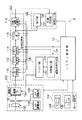
ディジタルスチルカメラ10には、図1に示すように、撮像系10A 、信号処理系10B 、駆動信号生成部10C 、信号出力系10D 、モード指定部10E およびシステム制御部12が備えられている。
【0024】
撮像系10A には、撮像レンズ102 、撮像部104 、ピント調整機構を含むAF調整部106 および絞り機構を含むAE調整部108 が備えられている。この他、図示しないが撮像部104 の入射光の側に入射光を完全に遮光するためシャッタ機構を含めてもよい。撮像レンズ102 は、被写界からの入射光を撮像部104 の受光面上に焦点を結ぶように集光する光学系である。
【0025】
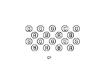
撮像部104 は、供給される入射光を光電変換する受光素子104aで受光面が形成されるように行方向および列方向にハニカム型に2次元配列されている(図2を参照)。ハニカム型とは、受光素子104aのそれぞれのうちで、斜めに隣接する素子のピッチを行方向および列方向に1/2 ずつずらした相互の位置関係に配された配置をいう。受光素子の形状を示すものではない。撮像部104 には、受光素子104aより入射光の側に入射光を色分解する色フィルタが受光素子104aのそれぞれに対応した色分解フィルタCFが単板で一体的に形成されている。この色分解フィルタCFの配設により、受光素子104aには、たとえば、三原色RGB というそれぞれの色の属性を有するように色分解された入射光が入射することになる。この関係は図3において一体的に形成されているので、各受光素子104a内に色を示す記号R, G, B で表している。また、図3の色フィルタR, G, B の配列は、色G に着目すると正方格子状に配置され、色R, Bは、色G を挟んで対角位置に同色の色フィルタを配置するRB完全市松パターンに配置されている。このことから、この色フィルタ配置をハニカム型G 正方格子RB完全市松パターンと呼ぶ。撮像部104 は、撮像信号を信号処理系10B に出力する。
【0026】
さらに撮像部104 の構成を説明する。撮像部104 は、後述する駆動信号生成部10C からそれぞれ出力される駆動信号に応動する。各受光素子104aは、電荷結合素子(以下、CCD という)で構成されている。受光素子104aは、図4に示すように、受光素子に隣接配設された転送素子、すなわち垂直転送素子との間に、受光して変換した信号電荷を漏れないように信号読出しゲート(トランスファゲート)104bが形成されている。信号読出しゲート104bは電極を介して供給されるフィールドシフトパルスにより信号電荷を受光素子104aから垂直転送路104cに転送する。垂直転送路104cは、読み出した信号電荷を列方向、すなわち垂直方向に順次転送する。垂直転送により、信号電荷はラインシフトを介して行方向の転送素子、すなわち水平転送路104dに供給される。水平転送路104dは、駆動信号に応動してこの信号電荷をアンプ104eを介して前述したように信号処理系10B に出力する。
【0027】
ここで、垂直転送路104cは、垂直(列)方向に見ると、受光素子104aと受光素子104aの間に3つの転送素子が配されている。信号読出しゲート104bの接続された転送素子も含めて1ライン分の転送には4つの転送素子が用いられる。このことから、1ラインの転送には、駆動信号として4相の駆動信号が供給されることが判る。信号読出しゲート104bは、受光素子104aと垂直転送路104cとの間に配されている。また、ハニカム配置を採用し、斜めに受光素子(画素)間のピッチを1/2 ずつ縦横にずらしていることから、信号読出しゲート104bと垂直転送路104cの転送素子との配置関係は、2つの垂直転送路104cに着目すると、転送素子2つ分ずれた位置に配されている。すなわち、2つの垂直転送路104cにおける配置関係を見ると、図4では、たとえば、受光素子(色G )- 垂直転送素子(V1)、受光素子(色R )- 垂直転送素子(V3)、受光素子(色G )- 垂直転送素子(V5)、・・・・というような関係で配設されている。撮像部104 の基本的な構成は以上のような関係である。この構成で通常は全画素読出しが行われる。これにより、一度に全画素の信号電荷を読み出している。
【0028】
AF調整部106 は、ピント調整機構(図示せず)により被写体とカメラ10との距離を測距して得られた情報に応じて撮像レンズ102 を最適な位置に配するようにこの位置調整を行う。このとき、測距情報の算出とこの測距情報からの制御量は、システム制御部12で処理される。この結果、供給される制御信号に応じてAF調整部106 は、ピント調整機構を駆動させ、撮像レンズ102 を移動させている。
【0029】
また、AE調整部108 は、被写体を含む被写界の測光値の算出が行われるシステム制御部12内に設けられる露光制御部(図示せず)からの制御により絞り機構の絞り位置を変位させ、入射する光束量を調整する。測光は、撮像信号の一部を用いている。この場合もシステム制御部12で測光値に基づいて露光量が算出され、この露光量になるように絞り値とシャッタ速度値を制御する制御信号を AE 調整部108 に供給する。AE調整部108 は、この制御信号に応じて絞り機構およびシャッタ機構をそれぞれ調整している。この調整により露出を最適にすることができる。
【0030】
信号処理系10B には、前処理部110 、A/D 変換部112 、信号処理部114 、バッファ部116 および圧縮/伸張処理部118 が備えられている。前処理部110 は、たとえば、供給される信号電荷に対して相関二重サンプリング(CDS )処理を施して雑音の低減を図ったり、信号にガンマ変換処理を施し、この信号を増幅させてA/D 変換部112 に出力する。
【0031】
A/D 変換部112 は、システム制御部12からの制御信号およびタイミング信号等を発生させる信号発生部120 からのクロック信号を用いて撮像部104 から供給されるアナログ信号をサンプリングし、量子化することによってディジタル信号に変換する。変換したディジタル信号は信号処理部114 に供給される。
【0032】
信号処理部114 は、得られた信号に自動絞り調整(AE)、白バランス調整(AWB )、アパーチャ補正等を行った後、信号処理を2つのモードそれぞれに応じて施す。すなわち、ここでのモードとは、後述するモード指定部10E のレリーズシャッタ128 で設定されたモードを示し、少なくとも得られた静止画を信号出力系10D の記録再生部126 に取り込む静止画撮影モードと単に撮像系10A のAFにおける測光制御モードの2つを示す。ガンマ補正処理は、ここで行ってもよいし、さらに後段で行ってもよい。
【0033】
ディジタルスチルカメラ10において、現在、いずれのモードが選択されているかはシステム制御部12からの制御信号により制御される。このシステム制御部12の制御により、上述した信号処理後の信号には、静止画撮影モードで所定のディジタルに伴う信号処理、たとえば、輝度信号の高帯域化等が施される。一方、測光制御モードでは、供給される信号がディジタルであることを考慮してシステム制御部12により撮像部104 からの信号読出しを、たとえば、従来の読出し速度に比べて速く読み出す制御およびその処理等が行われる。この他、撮像信号を信号出力系10D の表示部124 に表示させるように垂直間引き処理等も行われる。信号処理部114 は、静止画撮影モードでの信号処理によって撮像部104 からの撮像信号を記録可能な映像信号にしている。そして、信号処理部114 は、表示・記録が選択されたモードの信号だけをバッファ部116 に出力する。
【0034】
バッファ部116 は、前述した信号処理部114 から供給される映像信号を所定の振幅に増幅するとともに、記録時における時間調整の機能なども有している。バッファ部116 は、システム制御部12内に配される記録制御部(図示せず)の制御により信号出力系10D または圧縮/伸張信号部118 に画像を出力している。
【0035】
圧縮/伸張信号部118 は、画像を記録する場合、システム制御部12に制御により画像信号が供給される。供給された画像信号には、たとえば、JPEG(Joint Photographic coding Experts Group )規格に基づく圧縮処理が施される。また、記録再生部126 から記録されていた信号を読み出して再生する場合、上述した圧縮処理の逆変換等の信号処理を施すことによって元の画像信号を再生し、表示部124 に出力する。
【0036】
駆動信号生成部10C には、信号発生部120 およびドライバ部122 が含まれる。信号発生部120 は、たとえば、現行の放送方式(NTSC/PAL)でディジタルスチルカメラ10が駆動するように発生させた原発振のクロックを基に同期信号を生成して信号処理部114 に供給する。信号発生部120 は、前処理部110 、A/D 変換部112 、バッファ部116 および圧縮/伸張処理部118 にもサンプリング信号や書込み/読出し信号のクロックとして信号が供給されている。
【0037】
信号発生部120 は、原発振のクロックから同期信号を生成し、さらにこれらの信号を用いて各種のタイミング信号を生成している。生成されるタイミング信号には、撮像部104 で得られた信号電荷の読出しに用いるタイミング信号、たとえば、垂直転送路の駆動タイミングを供給する垂直タイミング信号、水平転送路の駆動タイミングを供給する水平タイミング信号、フィールドシフトやラインシフトさせるタイミング信号等がある。また、AF調整部106 、AE調整部108 の動作を制御する際にも信号発生部120 からの信号を用いている(ここでは信号線をそれぞれあらわには図示せず)。このように各種の信号を前述した各部に出力するとともに、信号発生部120 は、垂直タイミング信号と水平タイミング信号とをドライバ部122 に供給する。この中で、信号発生部120 にシステム制御部12から測光制御モードの制御信号が供給された際に、信号発生部120 は、たとえば、必要に応じて(たとえば、測光制御モードで)受光素子の基板電圧、すなわちオーバーフロードレイン電圧を色R, Bの受光素子に対して高める信号も供給する。この信号が供給されることにより、色R, Bの受光素子には、信号電荷が全く生成されなかったと同じ状態を形成することができる。また、測光制御モードで信号発生部120 は、色G だけの信号電荷を読み出すようにトランスファゲート信号を生成する。測光制御モードが選択された際に信号発生部120 は、システム制御部12からの制御信号12A によりタイミング信号の生成を選択的に切り換える。ドライバ部122 は、それぞれの供給されるタイミングで駆動信号を生成する。一般的に、信号読出しする速度変更は、モードに応じてドライバ部122 から出力される垂直駆動信号が撮像部104 に供給され、たとえば、画面全体に対する駆動、色の選択的な駆動、色および領域を指定した駆動が行われることによって速度の変更が施される。
【0038】
ドライバ部122 は、特にモードが測光制御モードに設定された際に対応した駆動信号を出力する。駆動信号レベルをモードで変更するような場合、レベル切換スイッチを設けて切り換える。一般に、設定される電圧レベルは、たとえば、1V, 5V, 8V, 12V がある。ドライバ部122 は、信号発生部120 から供給されるタイミング信号に応じて駆動信号を生成している。ドライバ部122 は、垂直タイミング信号とトランスファゲート信号とを用いて3値の駆動信号を生成している。
【0039】
信号出力系10D には、表示部124 および記録再生部126 が備えられている。表示部124 には、たとえば、ディジタルRGB 入力によるVGA (Video Graphics Array)規格の液晶表示モニタなどが備えられている。記録再生部126 は、磁気記録媒体、メモリカード等に用いられる半導体メモリ、光記録媒体、または光磁気記録媒体に供給される映像信号を記録する。また、記録再生部126 は、記録した映像信号を読み出して表示部124 に表示させることもできる。なお、この記録再生部126 が記録媒体を着脱自在にできる場合、記録媒体だけ取りはずして外部の装置で記録した映像信号を再生表示させたり画像を印刷させるようにしてもよい。
【0040】
モード指定部10E には、レリーズシャッタ128 およびキースイッチ130 が備えられている。レリーズシャッタ128 には、本実施例において、2段押し機能を備えている。すなわち、第1段の半押し状態では、測光制御モードを指定して、システム制御部12にこのモード設定がなされていることを信号として供給し、第2段の全押し状態では、画像の取込みタイミングをシステム制御部12に提供するとともに、この操作によりシステム制御部12に画像の記録設定(静止画撮影モード)がなされたことを信号として供給する。また、レリーズシャッタ128 が電源オン状態で、かつ画像モニタ表示のスイッチ(図示せず)がオンになっている場合、システム制御部12は、表示部124 にムービーモードで動画表示するように制御する。また、キースイッチ130 は、十字キーで、表示部124 の画面に表示される画面内のカーソルを上下左右に移動させて項目・画像の選択等を行う。この選択した情報もシステム制御部12に送られる。
【0041】
システム制御部12は、カメラ全体の動作を制御するコントローラである。システム制御部12には、中央演算装置(CPU )が含まれている。システム制御部12は、レリーズシャッタ128 からの入力信号によりどのモードが選択されたかの判断を行う。また、システム制御部12は、キースイッチ130 からの選択情報により、カメラの画像信号に対する処理等の制御を行う。このように供給された情報に基づいてシステム制御部12は、この判断結果を基に駆動信号生成部10C の動作を制御する。システム制御部12には、図示しないが記録制御部を設けている。記録制御部は、システム制御部12からのタイミング制御信号に従いバッファ部116 および信号出力系10D の記録再生部126 の動作を制御している。
【0042】
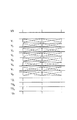
このように構成したディジタルスチルカメラ10の動作について説明する。まず、通常行われている全画素読出しについて説明する。ディジタルスチルカメラ10は、通常、全画素読出しを行える撮像部104 を有するカメラであるから、静止画撮影モードのモード指定がレリーズシャッタ128 から供給された場合、ハニカム型G 正方格子RG完全市松パターンの色分解フィルタCFを介した入射光が画素すべてで受光される。受光素子104aの各々では、この受光した際に受光素子104aで光電変換することによって信号電荷が蓄積される。蓄積された信号電荷を各受光素子104aから読み出す場合、図5に示すように、信号発生部120 では垂直同期信号VDが生成される。また、信号発生部120 では、垂直同期信号VDに同期させて垂直転送路104cの転送素子V1〜V4,V5〜V8に供給する垂直タイミング信号V1〜V8および信号読出しゲート104bに供給するトランスファゲート信号TG1, TG3, TG5, TG7が生成される。図5において、各垂直同期期間中、垂直タイミング信号V1, V4, V5, V8が立ち下がり信号であり、垂直タイミング信号V2, V3, V6, V7が立ち上がり信号であることが概略的に示されている。また、トランスファゲート信号TG1, TG3, TG5, TG7は、各受光素子から垂直同期信号VDの入力後に同期して信号電荷を読み出すように生成されていることが判る。このタイミング関係を時間的に拡大してみると、図6に示すタイミング関係にあることが判る。すなわち、ここでの段階ではトランスファゲートをオンにする際に垂直タイミング信号V1, V5に対応する位置の受光素子だけから信号電荷を読み出し、次の垂直同期信号VDが供給されるまでフィールドシフトが行われないことを示している(図5も参照)。そして、フィールドシフト後、水平同期信号HDに同期して各垂直タイミング信号が順次供給される。この供給により、垂直転送路104cにシフトされた信号電荷が水平転送路104dに向かって転送されていく。
【0043】
図6のタイミング関係において垂直同期信号VDがレベル"H" にレベル変化した後、水平同期信号HDが立ち上がった状態以降の垂直タイミング信号およびトランスファゲート信号の各タイミングを図7のタイミングチャートは時間的に拡大し、表示している(図7(a), (b)を参照)。特に、垂直タイミング信号V1, V5とトランスファゲート信号TG1, TG5とがドライバ部122 に供給されると、図7(c) に示す垂直駆動信号φV1, φV5が撮像部104 に出力される。これに伴って、垂直転送素子V1, V5には、図7(d) に示すポテンシャルが形成される。また、トランスファゲート信号TG3, TG7もオン状態になることから、図7(e) に示す垂直駆動信号φV3, φV7が生成される。これにより、ポテンシャルが図7(f) のように形成される。
【0044】
また、垂直転送路104cにシフトされた信号電荷が水平転送路104dに向かって転送されていく手順を、図8のタイミングチャートで示す。垂直転送路104cを8つの垂直転送素子V1〜V8で表している。この中で、垂直駆動信号は、垂直転送素子V1〜V4と垂直転送素子V5〜V8と2つ同じ信号が供給されていることが判る。すなわち、4つの異なる位相の信号で駆動させている。垂直転送された信号電荷にラインシフトが施された後、水平転送路104dを順次転送させて撮像部104 から全画素の信号電荷を所定の時間内に一度に読み出している。
【0045】
ところで、一般的なディジタルスチルカメラ10の撮影手順を検討してみる。まず、最初にディジタルスチルカメラ10では、撮影を行う前に被写界に対して測光を行う。被写界の撮像の際にレリーズシャッタ128 を半押し状態にして測光制御モードにする。この場合、撮像系10A の撮像部104 で光電変換して得られた信号のうち、色G だけを取り出す撮像を行う。これは、AFの調整制御を行う場合、輝度情報の約70% を占める色G の情報だけで済むことにある。また、AFの測光は、適正な値を検出するまで何度も画素情報を読み出す必要があるので、できるだけ高速に信号電荷を読み出したいという要求がある。一方、AE, AWB の調整制御を行う場合、全色情報が必要なので、このような単色の読出しを行っても意味をなさない。この撮像を行う際に駆動信号により高速の信号読出しが行われるがこの信号読出しついては後段でさらに詳述する。
【0046】
測光に伴って撮像系10A で得られた画像信号は、システム制御部12の制御により信号処理系10B に供給される。信号処理系10B では、供給された画像信号をディジタル信号に変換する。この変換により得られた画像データは、測光情報としてシステム制御部12に供給される。システム制御部12は、この測光情報を用いて演算を行う。この演算により、システム制御部12は、AFの調整用の制御信号を生成してそれぞれAF調整部106 に出力する。AF調整部106 は、内蔵する機構を介して、それぞれ供給される制御信号に応じた調整を行う。この調整は、このモードにおいて繰り返し行われる。
【0047】
この後、ユーザは所望の撮影タイミングでレリーズシャッタ128 を全押し状態にする。このとき、システム制御部12にこの被写界の映像を記録する信号が供給される。先のモードと同様に撮像系10A で被写界からの入射光の撮像が行われる。ただし、この静止画撮影モード(全画素読出し)では、色RGB すべてを取り出す処理が撮像部104 で行われる。この撮像の前に、当然、供給される駆動信号も先の信号読出しとは異なる。撮像した画像信号は、信号処理系10B のA/D 変換部112 でディジタル信号にされた後、信号処理部114 に供給される。信号処理部114 では、画像データに輝度信号、色差信号に対応する画像データが、周波数的に一層の高域側に延びた信号となるように信号処理を施す。そして、得られた画像データがバッファ部116 を介して圧縮/伸張処理部118 に供給される。圧縮/伸張処理部118 では、圧縮処理が施され、信号出力系10D に出力される。静止画撮影モードでは、システム制御部12内の記録制御部の制御により供給される全画素の画像データが記録再生部126 に記録される。記録再生部126 は、記録した画像データを記録制御部の制御により読み出すこともできる。
【0048】
このようにディジタルスチルカメラ10は、レリーズシャッタ128 によって測光制御モードおよび静止画撮影モードの両方に対応させている。ディジタルスチルカメラ10は、たとえば、100 万を越えるような高画素数で撮影する場合、静止画撮影モードは連写撮影するときを除いて、それほど撮像信号の全画素読出しの時間を気にしないが、測光制御モードでは、前述したようにAF制御を行うときに読出し時間の短縮に迫られる。このような仕様の撮像系10A を用いてディジタルスチルカメラ10にAF制御を施す測光制御モードでの撮像部104 および駆動信号生成部10C の動作について説明する。
【0049】
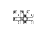
色分解フィルタCFにハニカム型G 正方格子RB完全市松パターンを採用しているので、図4から明らかなように、色G の受光素子104aは垂直転送素子V1, V5に隣接して配設されていることが判る。輝度情報の大部分を占める色G だけを読み出す場合、垂直転送素子V1, V5に隣接している信号読出しゲート104bをオンにするようにトランスファゲート信号TG1, TG5を供給すればよい。このタイミング関係を図9に示す。他のトランスファゲート信号TG3, TG7がレベル"H" にあるので、垂直転送素子V3, V7に隣接した信号読出しゲート104bはオフ状態のままで色R/B の信号電荷を読み出せない。この関係により図10(a) に示すように受光素子G1, G2から垂直転送路104cに信号電荷が読み出される。垂直転送路104cに読み出された信号電荷は、前述した通り順次水平転送路104dに向かって転送させる。このとき、垂直転送路104c内の信号電荷すべては、転送距離を2ライン分、下方に移動させる。この結果、水平転送路104dに最も近かった受光素子G1の信号電荷が水平転送路104dに供給される。したがって、受光素子G1の信号電荷は、2ラインの移動のうち、2ライン目の移動はラインシフトになっている。色R/B の信号電荷が読み出されないので、この信号電荷が入るはずの転送素子には「空」の表示をしている(図10(b) を参照)。次に、水平転送路104dに達した信号電荷G1, 空, G1, 空,・・・が、順次出力側に配されるアンプ104e(図10には図示せず)に向かって転送され、出力される。この後、垂直転送路104c内の残った信号電荷すべてが、再び2ライン分、下方に移動させる(図11(a) を参照)。そして水平転送路104dに達した信号電荷G1, 空, G1, 空,・・・が、順次出力側に配されるアンプ104eに向かって転送され、出力される(図11(b) を参照)。
【0050】
このような信号電荷の転送によって図12に示すように斜線の入った色G だけからの信号電荷を読み出している。図12の配置からこの1/2 間引きは、水平および垂直方向に1/2 の間引きとなる。しかしながら、この配置は、前述したようにハニカム配置で画素ずれのピッチが縦横に1/2 ピッチずつずれている関係にある。このことから 実際に読み出される画素数は、水平および垂直ともに1/2 ずつ間引いて全画素の1/4 間引きの画素数とはならない。信号電荷の垂直転送素子への読出しを行わないことでその転送素子には「空」として扱う際に実際の信号電荷と区別なく扱える。換言すれば、垂直転送ではこの信号電荷「空」を無視することができるが、水平方向の転送においては、信号電荷「空」も一つの転送素子の位置を占める「空」の信号電荷があるものとみなして転送が行われる。このため、水平方向の転送段数は間引きを行わない場合と同じである(図10(c) および図(b) を参照)。
【0051】
そこで、水平方向の転送段数も1/2 間引きされるように信号電荷の読出しを検討した結果、以下の手順で行う。図13(a) に示すように信号電荷を読み出す。この手順は図10(a) と同じである。次の垂直転送も図10(b) と同様に全体的に2ライン(2段)ずつ読み出した信号電荷を転送する(図13(b) を参照)。ここまでは先の手順と同じである。
【0052】
次に水平転送であるが、水平方向に転送路104d中を2段だけ移動させる。このため、水平転送路104dは、信号電荷が保持できるように転送素子を少なくとも、2段分余分に保有可能な構成にしている。この結果、色R/B の「空」の信号電荷が色G を転送する垂直転送路の直下に送られる(図13(c) を参照)。この後、前述したと同じ垂直転送を行う。これにより、残っている信号電荷が2段ずつ下方に転送される。色G を転送する垂直転送路の直下には、色R/B の「空」の信号電荷があるが、本来「空」であるので色G が転送されてきても混色になることはない。したがって、色R/B の信号電荷が入る領域に色G2が混色することなく入ることになる。この結果、色G の2ラインの信号電荷が水平転送路104d内に収められることになる。2回目の垂直転送後の水平転送は、この色G の2ラインの信号電荷G1, G2, G1, G2,・・・を水平転送路104dからすべて一度に読み出す。この転送処理により2ライン分の信号電荷が通常の1ライン分の読出し時間で読み出されることになる(図14を参照)。すなわち、水平方向における1/2 間引きが行われる。
【0053】
この手順で処理することにより、水平および垂直方向にそれぞれ1/2 ずつ間引きされるので、全画素読出しに要する時間に比べて所要時間を1/4 に短縮化して済ませることが容易にできる。
【0054】
ここで、色G を用い、制御する用途で最も高速性の要求されるAF制御について検討し、より一層の信号電荷の読出しを高速化する方法を考察する。このAF制御を行う上で要求される測光範囲は、画面全体でなく画面中央付近の領域で済ませることができる。画面中央付近の領域は、図15に示す斜線の領域104fで、画面全体に対して、少なくとも1/4 程度以上で半分以下程度である。このような領域に測光範囲を指定するのは、被写体が大体構図を考えるとき、画面中央付近に被写体を配することが多い経験的なものによっている。
【0055】
この指定範囲104fの色G の信号電荷だけを選択的に読み出すには、この指定範囲104f内の受光素子104aから信号電荷を読み出せるとよい。このため指定範囲104fとそれ以外の範囲を区別するように、供給する駆動信号を別々にする。指定範囲104fのそれ以外の範囲には、駆動信号φV1, φV5と区別するように駆動信号φV1a,φV5a にする。一方、指定範囲104fには、駆動信号φV1a,φV5a と区別するように駆動信号φV1b,φV5b にする。しかも、駆動信号φV1b,φV5b が供給される信号線は、指定範囲104fとそれ以外の範囲に供給される信号線と全く独立に配線されている。
【0056】
この場合の動作を簡単に図17〜図19を用いて説明する。画面中央付近の領域104fから色G を読み出すとき、領域104fに並行して配設している垂直転送素子V1,V5に駆動信号φV1a,φV5a を供給する。この駆動信号φV1a,φV5a は、図17の垂直タイミング信号V1, V5およびトランスファゲート信号TG1b, TG5bによって作成される。特に、トランスファゲート信号TG1b, TG5bが独立に生成され、かつこれらのタイミング信号がそれぞれに供給される。この場合、トランスファゲート信号TG1a, TG5aは生成されない。図17の垂直同期信号VDを含めた時間領域を拡大すると、垂直タイミング信号、トランスファゲート信号のそれぞれは、図18のタイミングチャートで表される。垂直タイミング信号V1〜V8は、前述した図6の垂直タイミング信号と同じである。また、トランスファゲート信号は、前述したようにトランスファゲート信号TG1, TG5を2つの領域用に分けて用いる。この図では、指定範囲104fだけから信号電荷を読み出すので、トランスファゲート信号TG1b, TG5bが供給される垂直転送素子V1, V5だけに信号電荷が読み出される。このようにして読み出す信号電荷の範囲を規定している。さらに、図18のトランスファゲート信号TG1b, TG5bの近傍の時間領域を拡大表示すると、図19に示すタイミング関係になっている。垂直タイミング信号V1, トランスファゲート信号TG1bと垂直タイミング信号V5, トランスファゲート信号TG5bが信号発生部120 からドライバ部122 に供給される。ドライバ部122 では、それぞれの組を用いて駆動信号φV1b,φV5b を生成する。この駆動信号がドライバ部122 から撮像部104 に供給される。図16に示すように指定範囲だけ信号電荷が受光素子104aから信号読出しゲート104bを介して垂直転送路104cの指定範囲104fに対応する垂直転送素子V1, V5に飛越し転送される。ここで、図16では、供給される駆動信号φV1b,φV5b が独立して供給されることを強調するため一本ずつしか配線を示していないが、この指定範囲104fに垂直転送素子V1, V5が他にもあれば、それぞれ駆動信号φV1b,φV5b が供給されることは言うまでもない。
【0057】
このようにして得られた信号電荷は、垂直転送され、前述した改良型の水平転送を行うと、信号電荷のより一層の高速読出しができるようになる。たとえば、全画素読出しの場合に比べて、最低必要な指定範囲を全画面の1/4 、改良型の水平転送を含む信号読出しによる水平および垂直方向の1/2 ずつの間引きを合わせて、 1/4× 1/2×1/2=1/16の時間だけで信号電荷を読み出すことができる。
【0058】
以上のように構成することにより、高画素化の要求を満たすために行ってきたことが二律背反的に高速の信号電荷の読出しを妨げている現状を比較的容易に解決することができる。これにより、撮像部からの信号電荷を最も高速に読み出す要求の高いAF制御に用いることができる。撮像部が測光センサの役割を果たしてくれるので、専用の測光センサを設けなくて済ませることができる。
【0059】
【発明の効果】
このように本発明の固体撮像装置によれば、モード指定手段でモードを設定し、この指定したモードの信号を制御手段に供給する。この供給により制御手段は、駆動信号生成手段を制御して駆動信号を生成する。撮像手段には、色フィルタG が列方向に配された色分解手段を介して入射光が供給される。撮像手段は、この入射光を各受光素子で光電変換し、指定のモードに応じて駆動信号生成手段から供給される駆動信号を信号読出し手段に供給し、信号電荷の飛越し転送を行う。この際に、色分解手段の色フィルタ配列を考慮して色G だけの信号読出しを行うことにより、高画素化された場合の信号読出しの所要時間の短縮化を図っている。撮像手段からの信号読出しを行い、たとえば、AFにおける情報の検出を行う場合、従来の読出し所要時間がかかり過ぎることが回避できる。測光専用に光学センサ等を用いるようなことをなくすことができる。
【0060】
また、本発明の信号読出し方法によれば、信号電荷の読出しを全画素読出しモードと色G だけの信号電荷を読み出す指定読出しモードかを選択し、この選択に応じて信号電荷の読出しに用いる所定のタイミングで動作させる駆動信号を生成させ、かつこの駆動信号の供給先を選択して供給する。また、入射光を三原色RGB にそれぞれ色分解し、この色分解工程で色分解された入射光を複数の受光素子のそれぞれで受光する。この撮像工程の後、特に、指定読出しモードでは複数の受光素子のうち、色G に対応する信号電荷だけを駆動信号によりフィールドシフトさせ、以降では飛越し転送された信号電荷を列方向に転送し、この信号電荷のラインシフトを経てこの信号電荷を水平方向に転送することにより、全画素読出しモードの信号読出しに比べて指定した色G だけの信号電荷の読出しで済ませることで所要時間を大幅に短縮させている。たとえば、高画素化してもこの方法をAFの測光制御に用いることができる。
【図面の簡単な説明】
【図1】本発明に係る固体撮像装置をディジタルスチルカメラに適用した際の概略的な構成を示すブロック図である。
【図2】図1の撮像部において、ハニカム配置された受光素子と垂直転送路の関係を説明する入射光側から見た模式図である。
【図3】図1の撮像部の入射光側に一体的に配されるハニカム型G 正方格子RB完全市松パターンの色分解フィルタのフィルタ配置を示す模式図である。
【図4】図1の撮像部において、受光素子、信号読出しゲート、垂直転送路の転送素子および水平転送路の接続関係ならびに供給される駆動信号の関係を示す模式図である。
【図5】図1の駆動信号生成部において全画素読出しを行う際に信号発生部で生成される垂直同期信号、垂直タイミング信号およびトランスファゲート信号のそれぞれの関係を説明するタイミングチャートである。
【図6】図5の垂直同期信号の立上がり近傍を時間的に拡大した際の垂直同期信号、垂直タイミング信号およびトランスファゲート信号のそれぞれの関係を説明するタイミングチャートである。
【図7】図6の水平同期信号の立上がり近傍を時間的に拡大した際の垂直同期信号、水平同期信号、垂直タイミング信号、トランスファゲート信号、駆動信号および駆動信号により生成されるポテンシャルのそれぞれの関係を説明するタイミングチャートである。
【図8】図1の撮像部の4相駆動の信号生成に用いる各垂直タイミング信号の位相関係を説明するタイミングチャートである。
【図9】図1の撮像部を測光制御モードで色G だけの信号電荷を読み出す駆動を行わせる際に信号発生部が生成す垂直同期信号、水平同期信号、垂直タイミング信号およびトランスファゲート信号のそれぞれの関係を説明するタイミングチャートである。
【図10】図9の信号発生部が生成した信号に基づいて供給された駆動信号に応動する信号電荷の読出しにおけるフィールドシフト、垂直転送および水平転送の各状態を説明する模式図である。
【図11】図10の信号読出しの後に行われる、垂直転送および水平転送の各状態を説明する模式図である。
【図12】図10および図11によって読み出される受光素子と読み出されない受光素子との位置関係を説明する模式図である。
【図13】図10および図11の改良型の間引き手順について垂直転送および水平転送の各状態を説明する模式図である。
【図14】図13の改良型の間引き手順の続きの状態を説明する模式図である。
【図15】図1の撮像部を測光制御モードのうち、AF調整の際に読み出す画面における指定範囲を示す模式図である。
【図16】図15の指定範囲から色G だけを読み出す際の受光素子、信号読出しゲート、垂直転送路の転送素子および水平転送路の接続関係ならびに供給される駆動信号の関係を示す模式図である。
【図17】図16の撮像部を駆動する際に信号発生部で生成される垂直同期信号、垂直タイミング信号およびトランスファゲート信号のそれぞれの関係を説明するタイミングチャートである。
【図18】図17の垂直同期信号の立上がり近傍を時間的に拡大した際の垂直同期信号、垂直タイミング信号およびトランスファゲート信号のそれぞれの関係を説明するタイミングチャートである。
【図19】図18の水平同期信号の立上がり近傍を時間的に拡大した際の垂直同期信号、水平同期信号、垂直タイミング信号、トランスファゲート信号および駆動信号のそれぞれの関係を説明するタイミングチャートである。
【符号の説明】
10 ディジタルスチルカメラ
12 システム制御部
10A 撮像系
10B 信号処理系
10C 駆動信号生成部
10D 信号出力系
10E モード指定部
104 撮像部
106 AF調整部
120 信号発生部
122 ドライバ部
104a 受光素子
104b 信号読出しゲート(トランスファゲート)
104c 垂直転送路
104d 水平転送路
104e 出力アンプ
V1〜V8 転送素子[0001]
BACKGROUND OF THE INVENTION
The present invention relates to a solid-state imaging device and a signal readout method that convert incident light into an electrical signal and capture an image of an object scene into the device, and in particular, in order to improve the resolution, the integration is highly integrated and adjacent to each other obliquely. It is suitable for use in imaging devices, that is, electronic still camera devices, image input devices, etc., in which pixels are arranged with a 1/2 pitch shift from each other with respect to the pixel center, so-called honeycomb-type pixel arrangement .
[0002]
[Prior art]
From the viewpoint of improving resolution through high integration, recently, as a new light receiving element arrangement, a so-called honeycomb arrangement in which the center of the geometric shape of the light receiving element is shifted by half the pitch in the row direction and the column direction is used. Various proposals have been made for solid-state imaging devices, such as Japanese Patent Publication No. 4-31231, Japanese Patent Application Laid-Open No. 6-77450, Japanese Patent Application Laid-Open No. 10-136391, and the like. In Japanese Examined Patent Publication No. 4-31231, the first electrode is meandered in a wavy pattern along the so-called light-sensitive means arranged so as to be shifted from the pixel, and the second electrode is formed in a pattern opposite in phase to the wavy pattern. In addition, another optical sensing means is disposed in a region where the first electrode and the second electrode are separated from each other, and selectively couples with the second electrode in response to an activation signal applied to the first electrode. By reading out the signal from the optical sensing means through the means, the resolution and sensitivity are improved as compared with the prior art. Here, the case where the optical sensor means is formed in an octagon is illustrated.
[0003]
In Japanese Patent Laid-Open No. 6-77450, the size of the light-receiving element is reduced to a small solid-state imaging device by increasing the aperture ratio by making each side a square, which is one of the rhombuses, so that each side forms an angle of 45 ° in the vertical direction. Is planned. In particular, vertical resolution is improved by adopting a honeycomb arrangement. Further, a microlens is disposed on each light receiving element to improve the light collection efficiency.
[0004]
Further, in Japanese Patent Laid-Open No. 10-136391, charge transfer is performed in the column direction of two columns between adjacent photoelectric conversion elements in the same row, with a relative shift of approximately 1/2 of the arrangement interval of the photoelectric conversion elements in adjacent rows. The device is arranged, one of which is formed by meandering the charge transfer device used for charge transfer from the photoelectric conversion element adjacent in the oblique direction, so that the photoelectric conversion element is highly integrated, the light receiving light rate is improved, etc. In this way, false signals such as moire are suppressed. In the above-mentioned Japanese Patent Publication No. 4-31231 and Japanese Patent Laid-Open No. 6-77450, attention is paid only to the device structure for high integration. Japanese Patent Application Laid-Open No. 10-136391 describes the structure of the device, the shape of the device, and the arrangement relationship of the color filters. Then, there is a description of all pixel readout using these relationships.
[0005]
[Problems to be solved by the invention]
By the way, with such high integration, there is a concern that it takes time to read out signal charges obtained by photoelectric conversion. For example, in a photometric control mode where auto focus adjustment (AF) or automatic exposure control (AE) is performed, it is necessary to shorten the time required to read out the signal charge and complete the preparation for imaging immediately. There is a request. For imaging devices, high integration of imaging elements and shortening of signal readout are contradictory requirements that are contradictory to each other. In particular, when a signal is read out at high speed in a photometric control mode from an imaging device having a honeycomb arrangement, a breakthrough by a different method from before is required.
[0006]
The present invention provides a solid-state imaging device and a signal readout method that can eliminate such drawbacks of the prior art and shorten the signal readout in the case of photometry control, for example, even if the image sensor is highly integrated. The purpose is to do.
[0007]
[Means for Solving the Problems]
In order to solve the above-described problem, the present invention provides a two-dimensional arrangement of a plurality of light-receiving elements that photoelectrically convert the incident light on a condensing surface on which incident light is collected, and each of the plurality of light-receiving elements. The elements that are diagonally adjacent to each other are arranged in a mutual positional relationship in which the pitch is shifted by 1/2 in the row direction and the column direction, and the signal charges obtained by photoelectric conversion in each of the plurality of light receiving elements are transferred to the respective elements. In a solid-state imaging device that converts an imaging signal output from an imaging unit that transfers in response to a drive signal at a predetermined timing into a digital signal, and performs signal processing on the signal to generate an image signal, Of the color filters that separate light into the three primary colors RGB, only the color separation means in which at least the color filter G is arranged in the column direction and the transfer element in the column direction arranged corresponding to each of the plurality of light receiving elements. Trust Signal readout means for interleaving and transferring signal charges, and among the modes representing the readout operation of signal charges from the imaging means in this apparatus, all-pixel readout mode for reading out signal charges from all of the plurality of imaging devices and only color G The mode designation means for designating one of the designated read modes, and the drive signal is generated according to the instruction of the mode designation means, and the supply destination of the drive signal generated according to the mode is selected. A drive signal generating means to be supplied; and a control means for controlling the generation of the drive signal for each mode to the drive signal generating means in response to an instruction from the mode specifying means and also controlling the signal processing applied to the imaging signal. It is characterized by including.
[0008]
Here, the color separation means arranges the color G in the color filter in a stripe shape in the color filter, and the color G is arranged in a square lattice shape, and the same color R, Alternatively, use a checkered pattern in which B is arranged in a completely checkered pattern or in a color G square lattice, with different colors R and B diagonally across the color G, and the same color filter in the same row. preferable. Thereby, when only the color G is taken out, color mixing can be avoided.
[0009]
Preferably, the drive signal generating means selectively supplies the drive signal only to the signal read means adjacent to the light receiving element corresponding to the color G of the color filter in the designated read mode.
[0010]
Further, the drive signal generating means is at least approximately symmetrical from the center in the column direction of the effective screen constituting the image among the signal read means to which the drive signal is further selectively supplied in the designated read mode. It is desirable to supply an independent designated drive signal only to the signal reading means in a predetermined area of 1/4 or more. As a result, since the signal charge readout region can be specified narrowly, the time required for further reading out the signal charge can be reduced according to the size of the region.
[0011]
The image pickup means uses a plurality of transfer elements arranged in the column direction as a unit, and is adjacent to the light receiving element of the color filter of color G among the electrodes to which a drive signal of a predetermined timing is supplied corresponding to each transfer element. The signal readout means for performing field shift is disposed only on the two electrodes, and the designated electrodes corresponding to the two electrodes arranged in a predetermined region are independent of the drive signal supplied in the all-pixel readout mode. It is preferable that the designated drive signal is supplied by wiring.
[0012]
Then, the signal reading means is arranged in the first and fifth transfer elements for the color G among the eight transfer elements, and in the third and seventh transfer elements in the column including both the colors R and B. It is good to install.
[0013]
In the solid-state imaging device of the present invention, a mode is set by the mode specifying unit, and a signal of the specified mode is supplied to the control unit. With this supply, the control unit controls the drive signal generation unit to generate a drive signal. Incident light is supplied to the imaging means through color separation means in which
[0014]
Further, according to the present invention, a plurality of light receiving elements that photoelectrically convert incident light are two-dimensionally arranged on a condensing surface on which incident light is collected, and the plurality of light receiving elements are adjacent to each other obliquely. Are arranged in a positional relationship in which the pitch between the light receiving elements is shifted by 1/2 in the row direction and the column direction, and the signal charges obtained by photoelectric conversion in each of the plurality of light receiving elements are In a signal readout method for converting an image pickup signal obtained by transfer by a drive signal into a digital signal and performing signal processing on the signal to generate an image signal, all of the plurality of image pickup elements are used in a mode representing a signal charge read operation. Specify either one of the all-pixel readout mode for reading out signal charges from the specified readout mode and the designated readout mode for reading out signal charges for only this color G among the three primary colors RGB A mode designation step to generate, a drive signal is generated in accordance with an instruction of the mode designation step, a drive signal supply step to select and supply a supply destination of the drive signal, and incident light is separated into three primary colors RGB A color separation process, an imaging process in which incident light separated in this color separation process is received by each of the plurality of light receiving elements, and after this imaging process, each pixel is obtained in each of the plurality of light receiving elements in the all-pixel readout mode. The signal charges are all read in response to the supplied drive signal, and in the designated read mode, the field in response to the drive signal supplied with only the signal charge from the light receiving element corresponding to color G among the plurality of light receiving elements. A shift process for shifting, a column transfer process for transferring signal charges transferred in the shift process in the column direction in response to a supplied drive signal, and this column transfer After allowed to line shift sends a signal charge at the end of the transfer by extent, characterized in that it comprises a horizontal transfer step of transferring in response to a drive signal supplied to the signal charges in the horizontal direction.
[0015]
Here, the drive signal supply step generates a field shift signal for reading the signal charges from the light receiving element of the color filter color G in the designated read mode, and supplies the field shift signal. A column transfer timing signal for generating a column transfer timing signal for transferring the signal charge in the column direction by two lines is generated, and this timing signal is supplied to the column signal supply step. After the transfer, the transferred signal charge is transferred in the row direction, and a row transfer timing signal to be output is generated, and the signal charge of the color G is read by repeating the row signal supply process for supplying this timing signal. Is desirable. Thus, the so-called half-thinning readout thinned out by one line for the entire screen can be easily performed without mixing other colors.
[0016]
In the row signal supply step, a row transfer timing signal for generating two columns of transfer distances for transferring the transferred signal charges in the row direction is generated, and the row signal supply step for supplying this timing signal is repeated 2 It is preferable to read out all signal charges of color G in the second row signal supply step. As a result, it is possible to provide improved decimation that reads out signal charges for two lines obtained by 1/2 decimation in a time for reading out one line.
[0017]
Further, the drive signal supplying step is performed at least when the signal charge is read from the light receiving element of the color filter color G in the designated readout mode, at least on the screen of the effective screen constituting the image almost symmetrically from the center in the column direction. Preferably, only a predetermined area of 1/4 or more is designated as the signal charge designated readout area, and the drive signal supplied to this designated readout area is supplied as an independent designated electrode drive signal. As a result, when the modes are different, a drive signal corresponding to each read request can be supplied, so that a signal charge read operation can be performed. In the shift step, a plurality of transfer elements arranged in the column direction are prepared in units of eight, and two electrodes corresponding to the color G among the electrodes to which a drive signal of a predetermined timing is supplied corresponding to each transfer element. In the all-pixel read mode, among the eight transfer elements in the all-pixel read mode, the
[0018]
In the shift process, the other drive signal supplied to the first and fifth transfer elements in the designated readout region in the designated readout mode is for an independent designated electrode that is distinguished from the one drive signal in the all-pixel readout mode. It is preferable to use it as a drive signal. As a result, signal reading in areas other than the designated readout area can be prohibited, and the signal readout of the color G signal charge can be performed only from the designated readout area in the designated readout mode.
[0019]
The drive signal supply process is substantially symmetrical from the center in the column direction of the effective screen constituting the image when the signal charge is read from the light receiving element of the color filter color G in the designated readout mode while performing the improved thinning. Furthermore, at least a predetermined area of 1/4 or more of this screen is designated as a signal charge designated readout area, and a drive signal supplied to this designated readout area is supplied as an independent designated electrode drive signal. It is preferable. The signal charge for two lines obtained by 1/2 decimation is read out in the time required to read out one line, and the signal read-out of the color G signal charge is performed only from the designated reading area, thereby further shortening the reading time. be able to.
[0020]
The signal readout method of the present invention selects either the all-pixel readout mode or the designated readout mode for reading out the signal charge of only the color G, and operates at a predetermined timing used for reading out the signal charge according to this selection. A drive signal to be generated is generated, and a supply destination of the drive signal is selected and supplied. Further, the incident light is color-separated into the three primary colors RGB, and the incident light color-separated in this color separation process is received by each of the plurality of light receiving elements. After this imaging process, in particular, in the designated readout mode, only the signal charge corresponding to color G is field-shifted by the drive signal among the plurality of light receiving elements, and then the interlaced signal charge is transferred in the column direction. By transferring this signal charge in the horizontal direction via the line shift of this signal charge, the required time can be greatly reduced by reading the signal charge of only the specified color G compared to the signal reading in the all pixel readout mode. It is shortened.
[0021]
DETAILED DESCRIPTION OF THE INVENTION
Next, embodiments of a solid-state imaging device and a signal readout method according to the present invention will be described in detail with reference to the accompanying drawings.
[0022]
The solid-state imaging device according to the present invention has a high speed required for performing automatic control such as AF in an imaging unit provided with a plurality of light receiving elements when so-called honeycomb arrangement is performed to increase the number of pixels. In order to satisfy the above, the signal readout time is shortened compared to the case of reading out all pixels using only the color G of the three primary colors RGB. In particular, there is a feature that it is possible to further increase the speed by designating a signal readout region to be measured. The case where this solid-state imaging device is applied to the digital
[0023]
As shown in FIG. 1, the digital
[0024]
The
[0025]
The
[0026]
Further, the configuration of the
[0027]
Here, in the
[0028]
The
[0029]
The
[0030]
The
[0031]
The A /
[0032]
The
[0033]
In the digital
[0034]
The
[0035]
When recording an image, the compression /
[0036]
The drive signal generation unit 10C includes a
[0037]
The
[0038]
The
[0039]
The signal output system 10D is provided with a
[0040]
The
[0041]
The
[0042]
The operation of the digital
[0043]
The timing chart of FIG. 7 shows the timing of the vertical timing signal and the transfer gate signal after the state in which the horizontal synchronizing signal HD rises after the vertical synchronizing signal VD changes to the level “H” in the timing relationship of FIG. (See FIGS. 7 (a) and 7 (b)). In particular, the vertical timing signal V 1 , V Five And transfer gate signal TG 1 , TG Five Are supplied to the
[0044]
Further, a procedure in which the signal charge shifted to the
[0045]
By the way, the photographing procedure of a general digital
[0046]
An image signal obtained by the
[0047]
Thereafter, the user fully presses the
[0048]
As described above, the digital
[0049]
Since the honeycomb-type G square lattice RB perfect checkered pattern is adopted for the color separation filter CF, as is apparent from FIG. 4, the
[0050]
As shown in FIG. 12, the signal charge from only the shaded color G is read out by such signal charge transfer. From the arrangement shown in FIG. 12, this 1/2 decimation becomes 1/2 decimation in the horizontal and vertical directions. However, this arrangement has a relationship in which the pixel shift pitch is shifted by 1/2 pitch vertically and horizontally in the honeycomb layout as described above. For this reason, the number of pixels actually read out is not reduced to 1/4 of all pixels by thinning out both horizontally and vertically. By not reading the signal charge to the vertical transfer element, the transfer element can be handled without distinction from the actual signal charge when handled as “empty”. In other words, in the vertical transfer, this signal charge “empty” can be ignored, but in the horizontal transfer, the signal charge “empty” also has an “empty” signal charge that occupies the position of one transfer element. Transfer is performed as if it were a thing. For this reason, the number of transfer stages in the horizontal direction is the same as when no decimation is performed (see FIG. 10 (c) and FIG. 10 (b)).
[0051]
Therefore, as a result of studying readout of signal charges so that the number of horizontal transfer stages is also reduced by half, the following procedure is used. The signal charge is read out as shown in FIG. This procedure is the same as in FIG. 10 (a). In the next vertical transfer, the signal charges read out by two lines (two stages) are transferred as a whole as in FIG. 10B (see FIG. 13B). The procedure up to this point is the same as the previous procedure.
[0052]
Next, for horizontal transfer, the
[0053]
By processing in this procedure, the horizontal and vertical directions are each halved, so that the required time can be easily shortened to 1/4 compared to the time required for all pixel readout.
[0054]
Here, the AF control that requires the highest speed in the control application using the color G will be examined, and a method for further speeding up the reading of signal charges will be considered. The metering range required for this AF control can be limited to the area near the center of the screen, not the entire screen. The area near the center of the screen is a hatched
[0055]
In order to selectively read out only the signal charge of the color G in the designated
[0056]
The operation in this case will be briefly described with reference to FIGS. When reading the color G from the
[0057]
The signal charge thus obtained is vertically transferred, and if the above-described improved horizontal transfer is performed, the signal charge can be read at a higher speed. For example, compared to the case of all pixel readout, the minimum required specified range is 1/4 of the whole screen, and the horizontal and vertical decimation by signal readout including improved horizontal transfer is reduced by 1 every 1 The signal charge can be read out only in the time of / 4 × 1/2 × 1/2 = 1/16.
[0058]
By configuring as described above, it is possible to relatively easily solve the current situation that what has been done to meet the demand for higher pixel counts contradicts the high-speed reading of signal charges. Thereby, it can be used for AF control with a high demand for reading the signal charge from the imaging unit at the highest speed. Since the imaging unit plays the role of a photometric sensor, it is not necessary to provide a dedicated photometric sensor.
[0059]
【The invention's effect】
Thus, according to the solid-state imaging device of the present invention, the mode is set by the mode specifying means, and the signal of the specified mode is supplied to the control means. With this supply, the control unit controls the drive signal generation unit to generate a drive signal. Incident light is supplied to the imaging means through color separation means in which
[0060]
Further, according to the signal readout method of the present invention, the signal charge is read out by selecting between the all-pixel readout mode and the designated readout mode for reading out the signal charge of only the color G, and depending on this selection, the predetermined signal used for reading the signal charge is used. A drive signal to be operated at the timing is generated, and a supply destination of the drive signal is selected and supplied. Further, the incident light is color-separated into the three primary colors RGB, and the incident light color-separated in this color separation process is received by each of the plurality of light receiving elements. After this imaging process, in particular, in the designated readout mode, only the signal charge corresponding to color G is field-shifted by the drive signal among the plurality of light receiving elements, and then the interlaced signal charge is transferred in the column direction. By transferring this signal charge in the horizontal direction via the line shift of this signal charge, the required time can be greatly reduced by reading the signal charge of only the specified color G compared to the signal reading in the all pixel readout mode. It is shortened. For example, this method can be used for AF photometry control even when the number of pixels is increased.
[Brief description of the drawings]
FIG. 1 is a block diagram showing a schematic configuration when a solid-state imaging device according to the present invention is applied to a digital still camera.
2 is a schematic diagram viewed from an incident light side for explaining a relationship between a light receiving element arranged in a honeycomb and a vertical transfer path in the imaging unit of FIG. 1;
3 is a schematic diagram showing a filter arrangement of a color separation filter of a honeycomb-type G square lattice RB complete checkered pattern that is integrally arranged on the incident light side of the imaging unit of FIG. 1;
4 is a schematic diagram showing a connection relationship between a light receiving element, a signal readout gate, a transfer element of a vertical transfer path and a horizontal transfer path, and a relationship of supplied drive signals in the imaging unit of FIG.
5 is a timing chart for explaining a relationship among a vertical synchronization signal, a vertical timing signal, and a transfer gate signal generated by the signal generation unit when all the pixels are read out in the drive signal generation unit of FIG. 1;
6 is a timing chart for explaining the relationship among a vertical synchronizing signal, a vertical timing signal, and a transfer gate signal when the vicinity of the rising edge of the vertical synchronizing signal in FIG. 5 is expanded in time. FIG.
7 shows each of potentials generated by a vertical synchronizing signal, a horizontal synchronizing signal, a vertical timing signal, a transfer gate signal, a driving signal, and a driving signal when the vicinity of the rising edge of the horizontal synchronizing signal in FIG. 6 is expanded in time. It is a timing chart explaining a relationship.
8 is a timing chart for explaining the phase relationship of each vertical timing signal used for signal generation of the four-phase drive of the image pickup unit of FIG. 1;
9 shows a vertical sync signal, a horizontal sync signal, a vertical timing signal, and a transfer gate signal generated by the signal generator when the imaging unit shown in FIG. 1 is driven to read out signal charges of only color G in the photometric control mode. It is a timing chart explaining each relationship.
10 is a schematic diagram for explaining each state of field shift, vertical transfer, and horizontal transfer in reading of a signal charge that responds to a drive signal supplied based on a signal generated by a signal generation unit of FIG. 9;
11 is a schematic diagram for explaining each state of vertical transfer and horizontal transfer performed after the signal reading in FIG. 10;
12 is a schematic diagram for explaining the positional relationship between the light receiving elements read out according to FIGS. 10 and 11 and the light receiving elements not read out. FIG.
13 is a schematic diagram for explaining each state of vertical transfer and horizontal transfer in the improved thinning procedure of FIGS. 10 and 11. FIG.
14 is a schematic diagram for explaining a state subsequent to the improved thinning-out procedure in FIG. 13; FIG.
15 is a schematic diagram showing a designated range on a screen that is read out during AF adjustment in the photometry control mode of the image pickup unit in FIG. 1; FIG.
16 is a schematic diagram showing a relationship between a light receiving element, a signal readout gate, a transfer element of a vertical transfer path, a horizontal transfer path, and a relationship of supplied drive signals when reading only the color G from the specified range of FIG. is there.
17 is a timing chart for explaining the relationship among a vertical synchronization signal, a vertical timing signal, and a transfer gate signal generated by a signal generation unit when driving the imaging unit in FIG. 16;
18 is a timing chart for explaining the relationship among a vertical synchronizing signal, a vertical timing signal, and a transfer gate signal when the vicinity of the rising edge of the vertical synchronizing signal in FIG. 17 is enlarged in terms of time.
19 is a timing chart for explaining the relationship among a vertical synchronization signal, a horizontal synchronization signal, a vertical timing signal, a transfer gate signal, and a drive signal when the vicinity of the rising edge of the horizontal synchronization signal in FIG. 18 is expanded in time. .
[Explanation of symbols]
10 Digital still camera
12 System controller
10A imaging system
10B signal processing system
10C drive signal generator
10D signal output system
10E mode specification part
104 Imaging unit
106 AF adjustment section
120 Signal generator
122 Driver section
104a photo detector
104b Signal readout gate (transfer gate)
104c Vertical transfer path
104d horizontal transfer path
104e output amplifier
V1 to V8 transfer element
Claims (13)
前記入射光を三原色RGB にそれぞれ色分解する色フィルタのうち、少なくとも色フィルタG が列方向に配された色分解手段と、
前記複数の受光素子のそれぞれに対応して蓄積した信号電荷をゲートの開閉により列方向の転送素子に読み出す信号読出し手段とを含み、
該装置は、前記撮像手段からの前記信号電荷の読出し動作を表すモードのうち、前記複数の撮像素子すべてから信号電荷を読み出す全画素読出しモードおよび前記色G だけを読み出す指定読出しモードのいずれか一方のモードを指定するモード指定手段と、
該モード指定手段の指示に応じて前記駆動信号を生成し、前記全画素読出しモードで前記信号読出し手段に対応する転送素子すべてに前記駆動信号を供給し、前記指定読出しモードに応じて生成した駆動信号を列方向に配設された所定の転送素子だけに供給する駆動信号生成手段と、
前記モード指定手段からの指示を受けて前記駆動信号生成手段に対してモード毎の前記駆動信号の生成を制御し、前記撮像信号に施される信号処理も制御する制御手段とを含むことを特徴とする固体撮像装置。A plurality of light receiving elements that photoelectrically convert the incident light are two-dimensionally arranged on a condensing surface on which incident light is collected, and each of the plurality of light receiving elements that are obliquely adjacent to each other has a pitch in the row direction. The signal charges obtained by photoelectric conversion in each of the plurality of light receiving elements are transferred in response to drive signals at respective predetermined timings. In a solid-state imaging device that converts an imaging signal output from an imaging unit into a digital signal and performs signal processing on the signal to generate an image signal, the imaging unit includes:
Among the color filters that separate the incident light into the three primary colors RGB, color separation means in which at least the color filter G is arranged in the column direction; and
Signal readout means for reading out signal charges accumulated corresponding to each of the plurality of light receiving elements to a transfer element in a column direction by opening and closing a gate ;
The apparatus is one of an all-pixel readout mode for reading out signal charges from all of the plurality of imaging elements and a designated readout mode for reading out only the color G among the modes representing the readout operation of the signal charges from the imaging means. Mode specifying means for specifying the mode of
The drive signal generated in response to an instruction from the mode designation unit, the drive signal supplied to all transfer elements corresponding to the signal readout unit in the all-pixel readout mode, and the drive generated in accordance with the designated readout mode Drive signal generation means for supplying signals only to predetermined transfer elements arranged in the column direction ;
Characterized in that it comprises a control means for the receiving instruction from the mode specifying means controls the generation of the drive signal of each mode to the driving signal generating means also controls signal processing performed on the imaging signal A solid-state imaging device.
該装置は、
前記所定の領域に配される前記2つの電極に対応する指定電極には、全画素読出しモードで供給される駆動信号とは独立な配線で前記指定駆動信号が供給されることを特徴とする固体撮像装置。The apparatus according to claim 1, wherein the imaging unit includes a plurality of transfer elements arranged in a column direction in units of eight, and the electrodes are supplied with the drive signal at the predetermined timing corresponding to each transfer element. The signal readout means for performing field shift only on the two electrodes adjacent to the light receiving element of the color filter of the color G,
The device
The designated drive signal is supplied to the designated electrode corresponding to the two electrodes arranged in the predetermined region by a wiring independent of the drive signal supplied in the all-pixel readout mode. Imaging device.
前記信号電荷の読出し動作を表すモードにおいて、前記複数の撮像素子すべてから信号電荷を読み出す全画素読出しモードおよび三原色RGB のうち、該色G だけの信号電荷を読み出す指定読出しモードのいずれか一方のモードを指定するモード指定工程と、
該モード指定工程の指示に応じて前記駆動信号を生成し、該駆動信号の供給先を選択して供給する駆動信号供給工程と、
前記入射光を三原色RGB にそれぞれ色分解する色分解工程と、
該色分解工程で色分解された入射光を前記複数の受光素子のそれぞれで受光する撮像工程と、
該撮像工程の後、前記全画素読出しモードでは前記複数の受光素子のそれぞれで得られた信号電荷を供給される駆動信号に応動してすべて読み出し、前記指定読出しモードにおいて前記複数の受光素子のうち、色G に対応する受光素子からの信号電荷だけを供給される駆動信号に応動してフィールドシフトさせるシフト工程と、
該シフト工程により飛越し転送された信号電荷を供給される駆動信号に応動して列方向に転送する列転送工程と、
該列転送工程により前記信号電荷を転送の末端に送ってラインシフトさせた後に、該信号電荷を供給される駆動信号に応動して水平方向に転送する水平転送工程とを含むことを特徴とする信号読出し方法。A plurality of light receiving elements for photoelectrically converting the incident light are two-dimensionally arranged on a condensing surface on which incident light is collected, and the plurality of light receiving elements are pitches between the light receiving elements with respect to the light receiving elements obliquely adjacent to each other. Are arranged in a positional relationship shifted by 1/2 in the row direction and in the column direction, and signal charges obtained by photoelectric conversion in each of the plurality of light receiving elements are transferred by drive signals at respective predetermined timings. In a signal readout method of converting an obtained imaging signal into a digital signal and performing signal processing on the signal to generate an image signal, the method includes:
In the mode representing the readout operation of the signal charge, one of the all-pixel readout mode for reading out the signal charge from all of the plurality of image sensors and the designated readout mode for reading out the signal charge of only the color G among the three primary colors RGB A mode specification process for specifying
Wherein generating a drive signal in response to an instruction of the mode designation step, the drive signal supply step of supplying select the destination of the driving signal,
A color separation step for separating the incident light into three primary colors RGB,
An imaging step of receiving the incident light separated in the color separation step by each of the plurality of light receiving elements;
After the imaging step, in the all-pixel readout mode, the signal charges obtained in each of the plurality of light receiving elements are all read in response to the supplied drive signal, and in the designated readout mode, , A shift process for field shifting in response to a drive signal supplied with only the signal charge from the light receiving element corresponding to color G;
A column transfer step of transferring the signal charge jumped and transferred in the shift step in the column direction in response to the supplied drive signal;
And a horizontal transfer step of transferring the signal charge in the horizontal direction in response to the drive signal supplied after the signal charge is sent to the end of transfer in the column transfer step and line-shifted. Signal readout method.
前記フィールドシフト信号を供給して前記信号電荷を列方向に転送する際の転送距離を2ライン分にする列転送のタイミング信号を生成し、該タイミング信号を供給する列信号供給工程と、
列方向に転送しラインシフトが行われた後、転送された信号電荷を行方向に転送し、出力させる行転送のタイミング信号を生成し、該タイミング信号を供給する行信号供給工程とを繰り返して前記色G の信号電荷を読み出すことを特徴とする信号読出し方法。8. The method according to claim 7, wherein the driving signal supplying step generates a field shift signal for reading a signal charge from the light receiving element of the color G of the color filter in the designated reading mode, and supplies the field shift signal. A shift signal supply process;
A column signal supply step of generating a column transfer timing signal for supplying the field shift signal and transferring the signal charge in the column direction to a transfer distance of two lines, and supplying the timing signal;
After transferring in the column direction and performing line shift, the transferred signal charge is transferred in the row direction, and a row transfer timing signal to be output is generated, and the row signal supply step for supplying the timing signal is repeated. A signal reading method, wherein the signal charge of the color G is read.
前記全画素読出しモードで前記8個単位における第1ないし第8の転送素子のうち、色G では第1および第5の転送素子に供給される一方の駆動信号、色R, Bの両方を含む列では、第3および第7の転送素子に供給される駆動信号により動作することを特徴とする信号読出し方法。8. The method according to claim 7, wherein in the shifting step, a plurality of transfer elements arranged in the column direction are prepared in units of eight, and the drive signal of the predetermined timing is supplied corresponding to each transfer element. Of these, the field shift is performed with only two electrodes corresponding to the color G 1, and the method includes:
Among the first to eighth transfer elements in the unit of 8 in the all-pixel read mode, the color G includes one drive signal supplied to the first and fifth transfer elements, both colors R and B. In the column, the signal reading method is characterized by operating by a drive signal supplied to the third and seventh transfer elements.
Priority Applications (2)
| Application Number | Priority Date | Filing Date | Title |
|---|---|---|---|
| JP02002899A JP3943273B2 (en) | 1999-01-28 | 1999-01-28 | Solid-state imaging device and signal readout method |
| US09/492,317 US6850277B1 (en) | 1999-01-28 | 2000-01-27 | Solid-state image pickup apparatus with high-speed photometry and a signal reading method therefor |
Applications Claiming Priority (1)
| Application Number | Priority Date | Filing Date | Title |
|---|---|---|---|
| JP02002899A JP3943273B2 (en) | 1999-01-28 | 1999-01-28 | Solid-state imaging device and signal readout method |
Publications (3)
| Publication Number | Publication Date |
|---|---|
| JP2000224598A JP2000224598A (en) | 2000-08-11 |
| JP2000224598A5 JP2000224598A5 (en) | 2005-06-16 |
| JP3943273B2 true JP3943273B2 (en) | 2007-07-11 |
Family
ID=12015630
Family Applications (1)
| Application Number | Title | Priority Date | Filing Date |
|---|---|---|---|
| JP02002899A Expired - Fee Related JP3943273B2 (en) | 1999-01-28 | 1999-01-28 | Solid-state imaging device and signal readout method |
Country Status (2)
| Country | Link |
|---|---|
| US (1) | US6850277B1 (en) |
| JP (1) | JP3943273B2 (en) |
Families Citing this family (6)
| Publication number | Priority date | Publication date | Assignee | Title |
|---|---|---|---|---|
| DE10226274B4 (en) * | 2002-06-06 | 2006-07-06 | Leica Microsystems (Schweiz) Ag | Method and system for evaluating an optical image |
| US20050073729A1 (en) * | 2002-06-06 | 2005-04-07 | Urs Schmid | Process and system for evaluating an optical recording |
| JP4094364B2 (en) * | 2002-07-19 | 2008-06-04 | 富士フイルム株式会社 | Solid-state imaging device and photometric method thereof |
| JP4136611B2 (en) * | 2002-11-07 | 2008-08-20 | 富士フイルム株式会社 | Solid-state image sensor |
| JP4183635B2 (en) * | 2004-02-16 | 2008-11-19 | 富士フイルム株式会社 | Solid-state imaging device |
| JP4324502B2 (en) * | 2004-03-29 | 2009-09-02 | 富士フイルム株式会社 | CCD solid-state image sensor and digital camera |
Family Cites Families (15)
| Publication number | Priority date | Publication date | Assignee | Title |
|---|---|---|---|---|
| US4876590A (en) * | 1988-06-17 | 1989-10-24 | Eastman Kodak Company | Low resolution verifier for a still video image |
| EP0441345B1 (en) * | 1990-02-07 | 1995-10-11 | Fuji Photo Film Co., Ltd. | High-definition still picture camera |
| JP2935901B2 (en) * | 1990-12-06 | 1999-08-16 | キヤノン株式会社 | Imaging device |
| JPH0677450A (en) | 1992-06-25 | 1994-03-18 | Sony Corp | Solid-state image pickup element |
| US5493335A (en) * | 1993-06-30 | 1996-02-20 | Eastman Kodak Company | Single sensor color camera with user selectable image record size |
| US5751354A (en) * | 1994-04-28 | 1998-05-12 | Canon Kabushiki Kaisha | Image sensing apparatus and method with exposure performed based on focus evaluation values |
| US5563658A (en) * | 1994-12-16 | 1996-10-08 | Eastman Kodak Company | Electronic camera with rapid automatic focus of an image upon an image sensor |
| US5668597A (en) * | 1994-12-30 | 1997-09-16 | Eastman Kodak Company | Electronic camera with rapid automatic focus of an image upon a progressive scan image sensor |
| US20020057349A1 (en) | 1996-03-06 | 2002-05-16 | Masanori Yamaguchi | Image pickup apparatus and solid state image pickup device |
| JP3800673B2 (en) * | 1996-06-24 | 2006-07-26 | ソニー株式会社 | Solid-state imaging device and driving method thereof |
| JP3906496B2 (en) * | 1996-08-02 | 2007-04-18 | ソニー株式会社 | Solid-state imaging device, driving method thereof, and camera |
| JP3830590B2 (en) | 1996-10-30 | 2006-10-04 | 株式会社東芝 | Solid-state imaging device |
| US6452632B1 (en) * | 1997-01-31 | 2002-09-17 | Kabushiki Kaisha Toshiba | Solid state image sensor and video system using the same |
| JPH11164206A (en) * | 1997-12-01 | 1999-06-18 | Fuji Film Microdevices Co Ltd | Solid-state image pickup element and charge transfer method |
| JP2894341B1 (en) * | 1998-03-12 | 1999-05-24 | 日本電気株式会社 | Driving method of solid-state imaging device |
-
1999
- 1999-01-28 JP JP02002899A patent/JP3943273B2/en not_active Expired - Fee Related
-
2000
- 2000-01-27 US US09/492,317 patent/US6850277B1/en not_active Expired - Fee Related
Also Published As
| Publication number | Publication date |
|---|---|
| US6850277B1 (en) | 2005-02-01 |
| JP2000224598A (en) | 2000-08-11 |
Similar Documents
| Publication | Publication Date | Title |
|---|---|---|
| US6829008B1 (en) | Solid-state image sensing apparatus, control method therefor, image sensing apparatus, basic layout of photoelectric conversion cell, and storage medium | |
| JP4738907B2 (en) | Solid-state imaging device and solid-state imaging device | |
| US20070076269A1 (en) | Imaging unit and image sensor | |
| JP2006121650A (en) | Solid-state image pickup apparatus | |
| JP4291793B2 (en) | Solid-state imaging device and solid-state imaging device | |
| JPH10210367A (en) | Electronic image-pickup device | |
| US7609306B2 (en) | Solid-state image pickup apparatus with high- and low-sensitivity photosensitive cells, and an image shooting method using the same | |
| JP3970185B2 (en) | Solid-state image sensor and digital camera | |
| JP4639406B2 (en) | Imaging device | |
| JP2006270364A (en) | Solid-state image pickup element and solid-state image pickup device, and driving method thereof | |
| JP3893424B2 (en) | Solid-state imaging device and signal readout method | |
| JP2005072966A (en) | Solid-state image pickup device and image pickup apparatus | |
| JP3943273B2 (en) | Solid-state imaging device and signal readout method | |
| JP2000224599A (en) | Solid-state image pickup device and signal reading method | |
| JP2008270832A (en) | Solid-state imaging element and imaging apparatus | |
| JP4195148B2 (en) | Solid-state imaging device and signal readout method | |
| JP3905308B2 (en) | Digital camera and operation control method thereof | |
| JP2007124174A (en) | Solid-state imaging apparatus and drive control method of solid-state imaging element | |
| JP4309618B2 (en) | Driving method of solid-state imaging device | |
| JP4630200B2 (en) | Solid-state imaging device and imaging apparatus | |
| JP2005020276A (en) | Solid-state image pickup element and image pickup device | |
| JP2005303653A (en) | Image pickup device | |
| JP2001078208A (en) | Solid-state image pickup device and signal read method | |
| JP2005012403A (en) | Digital camera and picture information acquisition method | |
| JP2008252935A (en) | Image pickup device |
Legal Events
| Date | Code | Title | Description |
|---|---|---|---|
| A521 | Request for written amendment filed |
Free format text: JAPANESE INTERMEDIATE CODE: A523 Effective date: 20040910 |
|
| A621 | Written request for application examination |
Free format text: JAPANESE INTERMEDIATE CODE: A621 Effective date: 20040910 |
|
| A977 | Report on retrieval |
Free format text: JAPANESE INTERMEDIATE CODE: A971007 Effective date: 20060914 |
|
| A131 | Notification of reasons for refusal |
Free format text: JAPANESE INTERMEDIATE CODE: A131 Effective date: 20061003 |
|
| A711 | Notification of change in applicant |
Free format text: JAPANESE INTERMEDIATE CODE: A712 Effective date: 20061129 |
|
| A521 | Request for written amendment filed |
Free format text: JAPANESE INTERMEDIATE CODE: A523 Effective date: 20061204 |
|
| TRDD | Decision of grant or rejection written | ||
| A01 | Written decision to grant a patent or to grant a registration (utility model) |
Free format text: JAPANESE INTERMEDIATE CODE: A01 Effective date: 20070313 |
|
| A61 | First payment of annual fees (during grant procedure) |
Free format text: JAPANESE INTERMEDIATE CODE: A61 Effective date: 20070405 |
|
| R150 | Certificate of patent or registration of utility model |
Free format text: JAPANESE INTERMEDIATE CODE: R150 |
|
| FPAY | Renewal fee payment (event date is renewal date of database) |
Free format text: PAYMENT UNTIL: 20110413 Year of fee payment: 4 |
|
| FPAY | Renewal fee payment (event date is renewal date of database) |
Free format text: PAYMENT UNTIL: 20120413 Year of fee payment: 5 |
|
| FPAY | Renewal fee payment (event date is renewal date of database) |
Free format text: PAYMENT UNTIL: 20130413 Year of fee payment: 6 |
|
| LAPS | Cancellation because of no payment of annual fees |